KR102013318B1 - Apparatus for thin layer deposition, method for manufacturing of organic light emitting display apparatus using the same, and organic light emitting display apparatus - Google Patents
Apparatus for thin layer deposition, method for manufacturing of organic light emitting display apparatus using the same, and organic light emitting display apparatusDownload PDFInfo
- Publication number
- KR102013318B1 KR102013318B1KR1020120104622AKR20120104622AKR102013318B1KR 102013318 B1KR102013318 B1KR 102013318B1KR 1020120104622 AKR1020120104622 AKR 1020120104622AKR 20120104622 AKR20120104622 AKR 20120104622AKR 102013318 B1KR102013318 B1KR 102013318B1
- Authority
- KR
- South Korea
- Prior art keywords
- hook
- deposition
- substrate
- organic layer
- chain
- Prior art date
- Legal status (The legal status is an assumption and is not a legal conclusion. Google has not performed a legal analysis and makes no representation as to the accuracy of the status listed.)
- Expired - Fee Related
Links
Images


Classifications
- C—CHEMISTRY; METALLURGY
- C23—COATING METALLIC MATERIAL; COATING MATERIAL WITH METALLIC MATERIAL; CHEMICAL SURFACE TREATMENT; DIFFUSION TREATMENT OF METALLIC MATERIAL; COATING BY VACUUM EVAPORATION, BY SPUTTERING, BY ION IMPLANTATION OR BY CHEMICAL VAPOUR DEPOSITION, IN GENERAL; INHIBITING CORROSION OF METALLIC MATERIAL OR INCRUSTATION IN GENERAL
- C23C—COATING METALLIC MATERIAL; COATING MATERIAL WITH METALLIC MATERIAL; SURFACE TREATMENT OF METALLIC MATERIAL BY DIFFUSION INTO THE SURFACE, BY CHEMICAL CONVERSION OR SUBSTITUTION; COATING BY VACUUM EVAPORATION, BY SPUTTERING, BY ION IMPLANTATION OR BY CHEMICAL VAPOUR DEPOSITION, IN GENERAL
- C23C14/00—Coating by vacuum evaporation, by sputtering or by ion implantation of the coating forming material
- C23C14/22—Coating by vacuum evaporation, by sputtering or by ion implantation of the coating forming material characterised by the process of coating
- C23C14/24—Vacuum evaporation
- C—CHEMISTRY; METALLURGY
- C23—COATING METALLIC MATERIAL; COATING MATERIAL WITH METALLIC MATERIAL; CHEMICAL SURFACE TREATMENT; DIFFUSION TREATMENT OF METALLIC MATERIAL; COATING BY VACUUM EVAPORATION, BY SPUTTERING, BY ION IMPLANTATION OR BY CHEMICAL VAPOUR DEPOSITION, IN GENERAL; INHIBITING CORROSION OF METALLIC MATERIAL OR INCRUSTATION IN GENERAL
- C23C—COATING METALLIC MATERIAL; COATING MATERIAL WITH METALLIC MATERIAL; SURFACE TREATMENT OF METALLIC MATERIAL BY DIFFUSION INTO THE SURFACE, BY CHEMICAL CONVERSION OR SUBSTITUTION; COATING BY VACUUM EVAPORATION, BY SPUTTERING, BY ION IMPLANTATION OR BY CHEMICAL VAPOUR DEPOSITION, IN GENERAL
- C23C14/00—Coating by vacuum evaporation, by sputtering or by ion implantation of the coating forming material
- C23C14/04—Coating on selected surface areas, e.g. using masks
- C23C14/042—Coating on selected surface areas, e.g. using masks using masks
- C—CHEMISTRY; METALLURGY
- C23—COATING METALLIC MATERIAL; COATING MATERIAL WITH METALLIC MATERIAL; CHEMICAL SURFACE TREATMENT; DIFFUSION TREATMENT OF METALLIC MATERIAL; COATING BY VACUUM EVAPORATION, BY SPUTTERING, BY ION IMPLANTATION OR BY CHEMICAL VAPOUR DEPOSITION, IN GENERAL; INHIBITING CORROSION OF METALLIC MATERIAL OR INCRUSTATION IN GENERAL
- C23C—COATING METALLIC MATERIAL; COATING MATERIAL WITH METALLIC MATERIAL; SURFACE TREATMENT OF METALLIC MATERIAL BY DIFFUSION INTO THE SURFACE, BY CHEMICAL CONVERSION OR SUBSTITUTION; COATING BY VACUUM EVAPORATION, BY SPUTTERING, BY ION IMPLANTATION OR BY CHEMICAL VAPOUR DEPOSITION, IN GENERAL
- C23C14/00—Coating by vacuum evaporation, by sputtering or by ion implantation of the coating forming material
- C23C14/22—Coating by vacuum evaporation, by sputtering or by ion implantation of the coating forming material characterised by the process of coating
- C23C14/24—Vacuum evaporation
- C23C14/243—Crucibles for source material
- C—CHEMISTRY; METALLURGY
- C23—COATING METALLIC MATERIAL; COATING MATERIAL WITH METALLIC MATERIAL; CHEMICAL SURFACE TREATMENT; DIFFUSION TREATMENT OF METALLIC MATERIAL; COATING BY VACUUM EVAPORATION, BY SPUTTERING, BY ION IMPLANTATION OR BY CHEMICAL VAPOUR DEPOSITION, IN GENERAL; INHIBITING CORROSION OF METALLIC MATERIAL OR INCRUSTATION IN GENERAL
- C23C—COATING METALLIC MATERIAL; COATING MATERIAL WITH METALLIC MATERIAL; SURFACE TREATMENT OF METALLIC MATERIAL BY DIFFUSION INTO THE SURFACE, BY CHEMICAL CONVERSION OR SUBSTITUTION; COATING BY VACUUM EVAPORATION, BY SPUTTERING, BY ION IMPLANTATION OR BY CHEMICAL VAPOUR DEPOSITION, IN GENERAL
- C23C14/00—Coating by vacuum evaporation, by sputtering or by ion implantation of the coating forming material
- C23C14/22—Coating by vacuum evaporation, by sputtering or by ion implantation of the coating forming material characterised by the process of coating
- C23C14/50—Substrate holders
- C—CHEMISTRY; METALLURGY
- C23—COATING METALLIC MATERIAL; COATING MATERIAL WITH METALLIC MATERIAL; CHEMICAL SURFACE TREATMENT; DIFFUSION TREATMENT OF METALLIC MATERIAL; COATING BY VACUUM EVAPORATION, BY SPUTTERING, BY ION IMPLANTATION OR BY CHEMICAL VAPOUR DEPOSITION, IN GENERAL; INHIBITING CORROSION OF METALLIC MATERIAL OR INCRUSTATION IN GENERAL
- C23C—COATING METALLIC MATERIAL; COATING MATERIAL WITH METALLIC MATERIAL; SURFACE TREATMENT OF METALLIC MATERIAL BY DIFFUSION INTO THE SURFACE, BY CHEMICAL CONVERSION OR SUBSTITUTION; COATING BY VACUUM EVAPORATION, BY SPUTTERING, BY ION IMPLANTATION OR BY CHEMICAL VAPOUR DEPOSITION, IN GENERAL
- C23C14/00—Coating by vacuum evaporation, by sputtering or by ion implantation of the coating forming material
- C23C14/22—Coating by vacuum evaporation, by sputtering or by ion implantation of the coating forming material characterised by the process of coating
- C23C14/56—Apparatus specially adapted for continuous coating; Arrangements for maintaining the vacuum, e.g. vacuum locks
- H—ELECTRICITY
- H10—SEMICONDUCTOR DEVICES; ELECTRIC SOLID-STATE DEVICES NOT OTHERWISE PROVIDED FOR
- H10H—INORGANIC LIGHT-EMITTING SEMICONDUCTOR DEVICES HAVING POTENTIAL BARRIERS
- H10H20/00—Individual inorganic light-emitting semiconductor devices having potential barriers, e.g. light-emitting diodes [LED]
- H10H20/80—Constructional details
- H10H20/81—Bodies
- H10H20/813—Bodies having a plurality of light-emitting regions, e.g. multi-junction LEDs or light-emitting devices having photoluminescent regions within the bodies
- H—ELECTRICITY
- H10—SEMICONDUCTOR DEVICES; ELECTRIC SOLID-STATE DEVICES NOT OTHERWISE PROVIDED FOR
- H10K—ORGANIC ELECTRIC SOLID-STATE DEVICES
- H10K50/00—Organic light-emitting devices
- H—ELECTRICITY
- H10—SEMICONDUCTOR DEVICES; ELECTRIC SOLID-STATE DEVICES NOT OTHERWISE PROVIDED FOR
- H10K—ORGANIC ELECTRIC SOLID-STATE DEVICES
- H10K50/00—Organic light-emitting devices
- H10K50/10—OLEDs or polymer light-emitting diodes [PLED]
- H10K50/11—OLEDs or polymer light-emitting diodes [PLED] characterised by the electroluminescent [EL] layers
- H—ELECTRICITY
- H10—SEMICONDUCTOR DEVICES; ELECTRIC SOLID-STATE DEVICES NOT OTHERWISE PROVIDED FOR
- H10K—ORGANIC ELECTRIC SOLID-STATE DEVICES
- H10K71/00—Manufacture or treatment specially adapted for the organic devices covered by this subclass
Landscapes
- Chemical & Material Sciences (AREA)
- Chemical Kinetics & Catalysis (AREA)
- Engineering & Computer Science (AREA)
- Materials Engineering (AREA)
- Mechanical Engineering (AREA)
- Metallurgy (AREA)
- Organic Chemistry (AREA)
- Physics & Mathematics (AREA)
- Optics & Photonics (AREA)
- Electroluminescent Light Sources (AREA)
- Physical Vapour Deposition (AREA)
Abstract
Translated fromKorean
Description
Translated fromKorean본 발명의 실시예들은 유기층 증착 장치, 이를 이용한 유기 발광 표시 장치의 제조 방법 및 유기 발광 표시 장치에 관한 것이다.Embodiments of the present invention relate to an organic layer deposition apparatus, a method of manufacturing an organic light emitting display device using the same, and an organic light emitting display device.
디스플레이 장치들 중, 유기 발광 디스플레이 장치는 시야각이 넓고 컨트라스트가 우수할 뿐만 아니라 응답속도가 빠르다는 장점을 가지고 있어 차세대 디스플레이 장치로서 주목을 받고 있다.Among the display devices, the organic light emitting display device has attracted attention as a next generation display device because of its advantages of having a wide viewing angle, excellent contrast, and fast response speed.
일반적으로, 유기 발광 디스플레이 장치는 애노드와 캐소드에서 주입되는 정공과 전자가 발광층에서 재결합하여 발광하는 원리로 색상을 구현할 수 있도록, 애노드와 캐소드 사이에 발광층을 삽입한 적층형 구조를 가지고 있다. 그러나, 이러한 구조로는 고효율 발광을 얻기 어렵기 때문에, 각각의 전극과 발광층 사이에 전자 주입층, 전자 수송층, 정공 수송층 및 정공 주입층 등의 중간층을 선택적으로 추가 삽입하여 사용하고 있다.In general, an organic light emitting display device has a stacked structure in which a light emitting layer is inserted between an anode and a cathode so that colors can be realized on the principle that holes and electrons injected from the anode and the cathode recombine in the light emitting layer to emit light. However, such a structure makes it difficult to obtain high-efficiency light emission. Therefore, intermediate layers such as an electron injection layer, an electron transport layer, a hole transport layer, and a hole injection layer are selectively inserted between each electrode and the light emitting layer.
본 발명의 주된 목적은 제조가 용이하고, 대형 기판 양산 공정에 용이하게 적용될 수 있으며, 제조 수율 및 증착 효율이 향상되고 기판 이송의 정밀도가 향상된 유기층 증착 장치, 이를 이용한 유기 발광 표시 장치의 제조 방법 및 유기 발광 표시 장치를 제공하는 것이다.The main object of the present invention is an organic layer deposition apparatus which is easy to manufacture, can be easily applied to a large-scale substrate mass production process, improves manufacturing yield and deposition efficiency, and improves substrate transfer accuracy, a method of manufacturing an organic light emitting display device using the same, and An organic light emitting display device is provided.
본 발명의 일 측면은, 기판 상에 유기층을 형성하는 유기층 증착 장치에 있어서, 증착 물질을 방사하는 증착원과, 상기 증착원의 일 측에 배치되며, 복수 개의 증착원 노즐들이 형성되는 증착원 노즐부와, 상기 증착원 노즐부와 대향되게 배치되고, 복수 개의 패터닝 슬릿들이 형성되는 패터닝 슬릿 시트와, 상기 기판을 탈부착할 수 있는 정전척과, 상기 정전척과 결합하여 상기 정전척을 이동시킬 수 있는 척 이동부재와, 상기 척 이동부재의 이동 방향을 가이드하는 가이드 부재를 구비하고, 상기 척 이동부재는 높이가 가변하는 후크부를 갖고, 상기 가이드 부재는 상기 후크부에 대응하여 체인부를 가지며, 상기 후크부가 상기 체인부에 삽입되어 상기 체인부의 작동에 따라 상기 척 이동부재가 상기 가이드 부재를 따라 이동하고, 상기 기판은 상기 패터닝 슬릿 시트와 소정 정도 이격되도록 형성되어 상기 유기층 증착 장치에 대하여 상대적으로 이동가능하도록 형성되는 것을 특징으로 하는 유기층 증착 장치를 제공할 수 있다.According to an aspect of the present invention, in an organic layer deposition apparatus for forming an organic layer on a substrate, a deposition source nozzle for emitting a deposition material, and a deposition source nozzle disposed on one side of the deposition source, the plurality of deposition source nozzles are formed And a patterning slit sheet disposed to face the deposition source nozzle portion, the plurality of patterning slits being formed, an electrostatic chuck capable of attaching and detaching the substrate, and a chuck capable of moving the electrostatic chuck in combination with the electrostatic chuck. And a guide member for guiding a moving direction of the chuck moving member, wherein the chuck moving member has a hook portion having a variable height, the guide member has a chain portion corresponding to the hook portion, and the hook portion The chuck moving member is moved along the guide member according to the operation of the chain part, and the substrate is inserted into the chain part. Turning slit is formed such that a sheet with a predetermined degree of spacing may provide an organic layer deposition apparatus being configured to be relatively moved with respect to said organic layer deposition device.
또한, 상기 체인부는, 상기 가이드 부재에 회전 가능하도록 설치되는 스프로켓과, 상기 스프로켓의 외면을 감싸도록 설치되는 타이밍 체인을 포함하는 것을 특징으로 할 수 있다.The chain part may include a sprocket rotatably installed on the guide member, and a timing chain installed to surround an outer surface of the sprocket.
또한, 상기 스프로켓은, 상기 타이밍 체인의 일단에 설치되는 제1 스프로켓과, 상기 타이밍 체인의 타단에 설치되는 제2 스프로켓을 구비하는 것을 특징으로 할 수 있다.The sprocket may include a first sprocket installed at one end of the timing chain and a second sprocket installed at the other end of the timing chain.
또한, 상기 체인부는, 상기 타이밍 체인의 내부에 설치되어 텐션(Tension)을 유지시키는 텐션유지유닛을 더 포함하는 것을 특징으로 할 수 있다.The chain part may further include a tension holding unit installed inside the timing chain to maintain a tension.
또한, 상기 타이밍 체인은 상기 가이드 부재의 길이 방향으로 설치되는 것을 특징으로 할 수 있다.In addition, the timing chain may be installed in the longitudinal direction of the guide member.
또한, 상기 체인부는, 상기 스프로켓과 연결되어 상기 스프로켓을 회전시키는 구동부를 더 구비하는 것을 특징으로 할 수 있다.The chain part may further include a driving part connected to the sprocket to rotate the sprocket.
또한, 상기 증착원, 상기 증착원 노즐부, 상기 패터닝 슬릿 시트, 상기 정전척, 상기 이동부재 및 상기 가이드 부재가 내부에 설치되는 챔버를 더 포함하고, 상기 구동부는 상기 챔버의 외부에 설치되어 상기 스프로켓과 샤프트로 연결되는 것을 특징으로 할 수 있다.The apparatus may further include a chamber in which the deposition source, the deposition source nozzle unit, the patterning slit sheet, the electrostatic chuck, the moving member, and the guide member are installed therein, and the driving unit is installed outside the chamber. It may be characterized in that it is connected to the sprocket and the shaft.
또한, 상기 후크부는, 상기 척 이동부재에 설치되는 후크하우징과, 상기 후크하우징을 선형 운동하도록 상기 후크하우징과 결합하는 후크와, 상기 후크하우징과 상기 후크에 설치되는 탄성부를 구비하는 것을 특징으로 할 수 있다.The hook unit may include a hook housing installed on the chuck moving member, a hook coupled to the hook housing to linearly move the hook housing, and the hook housing and an elastic unit installed on the hook. Can be.
또한, 상기 후크는 상기 체인부와의 접촉에 따라 상기 후크하우징의 높이 방향으로 선형 운동하는 것을 특징으로 할 수 있다.In addition, the hook may be characterized in that the linear movement in the height direction of the hook housing in accordance with the contact with the chain portion.
또한, 상기 척 이동부재와 상기 가이드 부재 사이에 LM(Linear motion) 가이드를 더 구비하는 것을 특징으로 할 수 있다.In addition, the linear motion (LM) guide may be further provided between the chuck moving member and the guide member.
또한, 상기 LM 가이드는, 상기 척 이동부재 상에 배치되는 가이드 블록과, 상기 가이드 부재 상에 배치되는 가이드 레일을 포함하며, 상기 가이드 블록은 상기 가이드 레일을 따라 이동하는 것을 특징으로 할 수 있다.The LM guide may include a guide block disposed on the chuck moving member and a guide rail disposed on the guide member, and the guide block may move along the guide rail.
또한, 상기 기판을 정전척으로 고정시키는 로딩부와, 상기 정전척으로부터 증착이 완료된 상기 기판을 분리시키는 언로딩부를 더 포함하는 것을 특징으로 할 수 있다.The apparatus may further include a loading unit to fix the substrate to the electrostatic chuck, and an unloading unit to separate the substrate from which the deposition is completed from the electrostatic chuck.
또한, 상기 후크부와 상기 체인부는 상기 정정척 및 상기 척 이동부재를 로딩부, 증착부 및 언로딩부로 순차적으로 이동시키는 것을 특징으로 할 수 있다.In addition, the hook portion and the chain portion may be characterized in that for moving the correcting chuck and the chuck moving member sequentially to the loading portion, the deposition portion and the unloading portion.
또한, 상기 증착원에서 방시된 상기 증착 물질은 상기 패터닝 슬릿 시트를 통과하여 상기 기판 상에 패턴을 형성하면서 증착되는 것을 특징으로 할 수 있다.In addition, the deposition material released from the deposition source may be deposited while forming a pattern on the substrate through the patterning slit sheet.
또한, 상기 유기층 증착 장치의 상기 패터닝 슬릿 시트는 상기 기판보다 작게 형성되는 것을 특징으로 할 수 있다.In addition, the patterning slit sheet of the organic layer deposition apparatus may be formed smaller than the substrate.
또한, 상기 증착원 노즐부에는 제1 방향을 따라 복수 개의 증착원 노즐들이 형성되고, 상기 패터닝 슬릿 시트에는 상기 제1 방향에 대해 수직인 제2 방향을 따라 복수 개의 패터닝 슬릿들이 형성되는 것을 특징으로 할 수 있다.The deposition source nozzles may include a plurality of deposition source nozzles in a first direction, and the patterning slit sheet may include a plurality of patterning slits in a second direction perpendicular to the first direction. can do.
본 발며의 일 측면은, 제1항의 유기층 증착 장치에 의해 제조된 유기 발광 표시 장치에 있어서, 상기 패터닝 슬릿 시트보다 큰 상기 기판과, 상기 기판 상에 상기 유기층 증착 장치에 의해 형성된 적어도 하나의 유기층을 구비하며, 상기 유기층은 리니어 패턴을 갖는 것을 특징으로 하는 유기 발광 표시 장치를 제공할 수 있다.One aspect of the present invention relates to an organic light emitting display device manufactured by the organic layer deposition apparatus of
또한, 상기 유기층은 발광층(emission layer)을 갖는 것을 특징으로 할 수 있다.In addition, the organic layer may be characterized by having an emission layer.
또한, 상기 유기층은 정공 주입층, 정공 수송층, 전자 수송층, 및 전자 주입층으로 이루어진 그룹에서 선택된 적어도 하나의 층을 구비하는 것을 특징으로 할 수 있다.In addition, the organic layer may be characterized in that it comprises at least one layer selected from the group consisting of a hole injection layer, a hole transport layer, an electron transport layer, and an electron injection layer.
또한, 상기 유기층들은 그 두께가 균일하지 않은 것을 특징으로 할 수 있다.In addition, the organic layers may be characterized in that the thickness thereof is not uniform.
본 발명의 일 측면은, 제1항에 유기층 증착 장치를 이용하여 형성된 두께가 균일하지 않은 적어도 하나의 유기층을 갖는 유기 발광 표시 장치를 제공할 수 있다.An aspect of the present invention can provide an organic light emitting display device having at least one organic layer having a non-uniform thickness formed by using the organic layer deposition apparatus in
본 발명의 일 측면은, 기판을 정전척에 고정시키는 단계와, 상기 정전척을 척 이동부재에 결합하는 단계와, 상기 척 이동부재는 가이드 부재를 따라 상기 정전척을 챔버 내로 이동하는 단계와, 상기 챔버 내에 배치된 유기층 증착 어셈블리와의 상대적인 이동에 의해 상기 기판 상에 유기층을 증착하는 단계를 구비하며, 상기 척 이동부재는 체인부와 후크부가 서로 연동하여 상기 가이드 부재를 따라 이동하며, 상기 기판은 상기 유기층 증착 어셈블리와 이격되는 것을 특징으로 하는 유기 발광 표시 장치의 제조 방법을 제공할 수 있다.One aspect of the invention, the step of fixing the substrate to the electrostatic chuck, coupling the electrostatic chuck to the chuck moving member, the chuck moving member to move the electrostatic chuck into the chamber along the guide member; And depositing an organic layer on the substrate by relative movement with the organic layer deposition assembly disposed in the chamber, wherein the chuck moving member moves along the guide member in association with the chain part and the hook part. May provide a method of manufacturing the organic light emitting diode display, which is spaced apart from the organic layer deposition assembly.
또한, 상기 척 이동부재는 높이가 가변하는 후크부를 구비하고, 상기 가이드 부재는 상기 후크부에 대응하여 체인부를 구비하는 것을 특징으로 할 수 있다.In addition, the chuck moving member may have a hook portion having a variable height, and the guide member may include a chain portion corresponding to the hook portion.
또한, 상기 체인부는, 상기 가이드 부재에 회전 가능하도록 설치되는 스프로켓과, 상기 스프로켓의 외면을 감싸도록 설치되는 타이밍 체인을 포함하는 것을 특징으로 할 수 있다.The chain part may include a sprocket rotatably installed on the guide member, and a timing chain installed to surround an outer surface of the sprocket.
또한, 상기 타이밍 체인은 상기 가이드 부재의 길이 방향으로 설치되는 것을 특징으로 할 수 있다.In addition, the timing chain may be installed in the longitudinal direction of the guide member.
또한, 상기 체인부는, 상기 스프로켓과 연결되어 상기 스프로켓을 회전시키는 구동부;를 더 구비하는 것을 특징으로 할 수 있다.The chain part may further include a driving part connected to the sprocket to rotate the sprocket.
또한, 상기 증착원, 상기 증착원 노즐부, 상기 패터닝 슬릿 시트, 상기 정전척, 상기 이동부재 및 상기 가이드 부재가 내부에 설치되는 챔버를 더 포함하고, 상기 구동부는 상기 챔버의 외부에 설치되어 상기 스프로켓과 샤프트로 연결되는 것을 특징으로 할 수 있다.The apparatus may further include a chamber in which the deposition source, the deposition source nozzle unit, the patterning slit sheet, the electrostatic chuck, the moving member, and the guide member are installed therein, and the driving unit is installed outside the chamber. It may be characterized in that it is connected to the sprocket and the shaft.
또한, 상기 후크부는, 상기 척 이동부재에 설치되는 후크하우징과, 상기 후크하우징을 선형 운동하도록 상기 후크하우징과 결합하는 후크와, 상기 후크하우징과 상기 후크에 설치되는 탄성부를 구비하는 것을 특징으로 할 수 있다.The hook unit may include a hook housing installed on the chuck moving member, a hook coupled to the hook housing to linearly move the hook housing, and the hook housing and an elastic unit installed on the hook. Can be.
또한, 상기 후크는 상기 체인부와의 접촉에 따라 상기 후크하우징의 높이 방향으로 선형 운동하는 것을 특징으로 할 수 있다.In addition, the hook may be characterized in that the linear movement in the height direction of the hook housing in accordance with the contact with the chain portion.
또한, 상기 정전척을 이동하는 단계는, 구동부에 의해 상기 샤프트를 회전하는 구동력을 발생하는 단계와, 상기 샤프트의 회전에 의해 스프로켓이 회전하면서 타이밍 체인을 회전시키는 단계와, 상기 타이밍 체인의 회전에 따라 후크가 상기 타이밍 체인에 삽입되어 상기 척 이동부재가 상기 가이드 부재를 따라 이동하는 것을 특징으로 할 수 있다.The moving of the electrostatic chuck may include generating a driving force for rotating the shaft by a driving unit, rotating the timing chain while the sprocket is rotated by the rotation of the shaft, and rotating the timing chain. Accordingly, a hook may be inserted into the timing chain to move the chuck moving member along the guide member.
상기한 바와 같이 이루어진 본 발명의 실시예들에 의하면, 제조가 용이하고, 대형 기판 양산 공정에 용이하게 적용될 수 있으며, 기판의 주행 정밀도, 제조 수율 및 증착 효율이 향상되는 효과를 얻을 수 있다.According to the embodiments of the present invention made as described above, it is easy to manufacture, can be easily applied to the mass production process of the substrate, it is possible to obtain the effect of improving the running precision, manufacturing yield and deposition efficiency of the substrate.
도 1은 본 발명의 일 실시예에 관한 유기층 증착 장치를 개략적으로 도시한 시스템 구성도이다.
도 2는 도 1의 정전척의 일 예를 도시한 개략도이다.
도 3은 본 발명의 일 실시예에 관한 유기층 증착 장치를 나타내는 사시도이다.
도 4는 도 3에 도시된 유기층 증착 장치를 나타내는 정면도이다.
도 5는 도 3에 도시된 유기층 증착 장치의 척 이동부재와 가이드 부재를 나타내는 사시도이다.
도 6은 도 5의 A부분을 보여주는 측면도이다.
도 7은 도 6에 도시된 후크부의 작동을 보여주는 개념도이다.
도 8은 도 1의 유기층 증착 장치의 유기층 증착 어셈블리를 개략적으로 도시한 사시도이다.
도 9는 도 8의 유기층 증착 어셈블리의 개략적인 측단면도이다.
도 10은 도 8의 유기층 증착 어셈블리의 개략적인 평단면도이다.
도 11은 본 발명의 다른 일 실시예에 관한 유기층 증착 어셈블리를 개략적으로 도시한 사시도이다.
도 12는 본 발명의 또 다른 일 실시예에 따른 유기층 증착 어셈블리를 개략적으로 도시한 사시도이다.
도 13은 본 발명의 유기층 증착 장치를 이용하여 제조된 액티브 매트릭스형 유기 발광 디스플레이 장치의 단면을 도시한 것이다.
도 14는 유기층 증착 장치에서 패터닝 슬릿 시트에 패터닝 슬릿들이 등 간격으로 형성되어 있는 모습을 나타내는 도면이다.
도 15는 도 14의 패터닝 슬릿 시트를 이용하여 기판상에 형성된 유기층을 나타내는 도면이다.1 is a system configuration diagram schematically showing an organic layer deposition apparatus according to an embodiment of the present invention.
FIG. 2 is a schematic diagram illustrating an example of the electrostatic chuck of FIG. 1.
3 is a perspective view showing an organic layer deposition apparatus according to an embodiment of the present invention.
FIG. 4 is a front view illustrating the organic layer deposition apparatus illustrated in FIG. 3.
FIG. 5 is a perspective view illustrating the chuck moving member and the guide member of the organic layer deposition apparatus illustrated in FIG. 3.
FIG. 6 is a side view illustrating portion A of FIG. 5.
FIG. 7 is a conceptual view illustrating the operation of the hook unit illustrated in FIG. 6.
FIG. 8 is a schematic perspective view of an organic layer deposition assembly of the organic layer deposition apparatus of FIG. 1.
9 is a schematic side cross-sectional view of the organic layer deposition assembly of FIG. 8.
10 is a schematic plan cross-sectional view of the organic layer deposition assembly of FIG. 8.
11 is a perspective view schematically showing an organic layer deposition assembly according to another embodiment of the present invention.
12 is a perspective view schematically showing an organic layer deposition assembly according to another embodiment of the present invention.
13 is a cross-sectional view of an active matrix organic light emitting display device manufactured using the organic layer deposition apparatus of the present invention.
FIG. 14 is a view illustrating patterning slits formed at equal intervals in a patterning slit sheet in an organic layer deposition apparatus. FIG.
FIG. 15 is a diagram illustrating an organic layer formed on a substrate using the patterning slit sheet of FIG. 14.
이하, 첨부한 도면을 참고로 하여 본 발명의 실시예에 대하여 본 발명이 속하는 기술 분야에서 통상의 지식을 가진 자가 용이하게 실시할 수 있도록 상세히 설명한다. 본 발명은 여러 가지 상이한 형태로 구현될 수 있으며 여기에서 설명하는 실시예에 한정되지 않는다.Hereinafter, exemplary embodiments of the present invention will be described in detail with reference to the accompanying drawings so that those skilled in the art may easily implement the present invention. As those skilled in the art would realize, the described embodiments may be modified in various different ways, all without departing from the spirit or scope of the present invention.
도 1은 본 발명의 일 실시예에 관한 유기층 증착 장치를 개략적으로 도시한 시스템 구성도이다.1 is a system configuration diagram schematically showing an organic layer deposition apparatus according to an embodiment of the present invention.
도 1을 참조하면, 본 발명의 일 실시예에 따른 유기층 증착 장치는 로딩부(710), 증착부(730), 언로딩부(720), 제1 순환부(610) 및 제2 순환부(620)를 포함한다.Referring to FIG. 1, an organic layer deposition apparatus according to an embodiment of the present invention may include a
로딩부(710)는 제1 래크(712)와, 도입로봇(714)과, 도입실(716)과, 제1 반전실(718)을 포함할 수 있다.The
제1 래크(712)에는 증착이 이루어지기 전의 기판(500)이 다수 적재되어 있고, 도입로봇(714)은 상기 제1 래크(712)로부터 기판(500)을 잡아 제2 순환부(620)로부터 이송되어 온 정전척(600)에 기판(500)을 얹은 후, 기판(500)이 부착된 정전척(600)을 도입실(716)로 옮긴다.The
도입실(716)에 인접하게는 제1 반전실(718)이 구비되며, 제1 반전실(718)에 위치한 제1 반전로봇(719)이 정전척(600)을 반전시켜 정전척(600)을 증착부(730)의 제1 순환부(610)에 장착한다.A
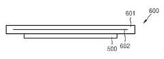
정전척(Electro Static Chuck, 600)은 도 2에서 볼 수 있듯이, 세라믹으로 구비된 본체(601)의 내부에 전원이 인가되는 전극(602)이 매립된 것으로, 이 전극(602)에 고전압이 인가됨으로써 본체(601)의 표면에 기판(500)을 부착시키는 것이다.As shown in FIG. 2, the
도 1에서 볼 때, 도입로봇(714)은 정전척(600)의 상면에 기판(500)을 얹게 되고, 이 상태에서 정전척(600)은 도입실(716)로 이송되며, 제1 반전로봇(719)이 정전척(600)을 반전시킴에 따라 증착부(730)에서는 기판(500)이 아래를 향하도록 위치하게 된다.As shown in FIG. 1, the
언로딩부(720)의 구성은 위에서 설명한 로딩부(710)의 구성과 반대로 구성된다. 즉, 증착부(730)를 거친 기판(500) 및 정전척(600)을 제2 반전실(728)에서 제2 반전로봇(729)이 반전시켜 반출실(726)로 이송하고, 반출로봇(724)이 반출실(726)에서 기판(500) 및 정전척(600)을 꺼낸 다음 기판(500)을 정전척(600)에서 분리하여 제2 래크(722)에 적재한다. 기판(500)과 분리된 정전척(600)은 제2 순환부(620)를 통해 로딩부(710)로 회송된다.The configuration of the
이때, 제1 순환부(610)와 제2 순환부(620)는 다양하게 배치될 수 있다. 예를 들면, 제1 순환부(610)와 제2 순환부(620)는 서로 동일 평면 상에 배치될 수 있다. 또한, 제1 순환부(610)와 제2 순환부(620)는 서로 다른 평면에 평행하게 배치될 수 있다. 이하에서는 설명의 편의를 위하여 제1 순환부(610)와 제2 순환부(620)가 동일 평면 상에 배치되는 경우를 중심으로 상세히 설명하기로 한다.In this case, the
한편, 본 발명은 반드시 이에 한정되는 것은 아니며, 기판(500)이 정전척(600)에 최초 고정될 때부터 정전척(600)의 하면에 기판(500)을 고정시켜 그대로 증착부(730)로 이송시킬 수도 있다. 이 경우, 예컨대 제1 반전실(718) 및 제1 반전로봇(719)과 제2 반전실(728) 및 제2 반전로봇(729)은 필요 없게 된다.Meanwhile, the present invention is not necessarily limited thereto, and since the
증착부(730)는 적어도 하나의 증착용 챔버를 구비한다. 도 1에 따른 본 발명의 일 실시예에 따르면, 상기 증착부(730)는 챔버(731)를 구비하며, 이 챔버(731) 내에 복수의 유기층 증착 어셈블리들(100)(200)(300)(400)이 배치된다. 도 1에 도시된 본 발명의 일 실시예에 따르면, 상기 챔버(731) 내에 제1 유기층 증착 어셈블리(100), 제2 유기층 증착 어셈블리(200), 제3 유기층 증착 어셈블리(300) 및 제4 유기층 증착 어셈블리(400)의 네 개의 유기층 증착 어셈블리들이 설치되어 있으나, 그 숫자는 증착 물질 및 증착 조건에 따라 가변 가능하다. 상기 챔버(731)는 증착이 진행되는 동안 진공으로 유지된다.The
한편, 도 1에 따른 본 발명의 일 실시예에 따르면, 상기 기판(500)이 고정된 정전척(600)은 제1 순환부(610)에 의해 적어도 증착부(730)로, 바람직하게는 상기 로딩부(710), 증착부(730) 및 언로딩부(720)로 순차 이동되고, 상기 언로딩부(720)에서 기판(500)과 분리된 정전척(600)은 제2 순환부(620)에 의해 상기 로딩부(710)로 환송된다.Meanwhile, according to one embodiment of the present invention according to FIG. 1, the
상기 제1 순환부(610)는 상기 증착부(730)를 통과할 때에 상기 챔버(731)를 관통하도록 구비되고, 상기 제2 순환부(620)는 정전척이 이송되도록 구비된다.The
도 3은 도 1의 유기층 증착 장치의 제1 순환부 및 제1 유기층 증착 어셈블리를 개략적으로 나타내는 사시도이고, 도 4는 도 3의 평면도이다. 여기서, 도 3에서는 설명의 편의를 위하여 제1 챔버가 생략된 상태로 도시되어 있다.3 is a perspective view schematically illustrating a first circulation portion and a first organic layer deposition assembly of the organic layer deposition apparatus of FIG. 1, and FIG. 4 is a plan view of FIG. 3. Here, in FIG. 3, for convenience of description, the first chamber is omitted.
도 3 및 도 4를 참조하면, 본 발명의 일 실시예에 관한 유기층 증착 장치는 제1 순환부(610)와 유기층 증착 어셈블리(1100)를 포함한다.3 and 4, an organic layer deposition apparatus according to an embodiment of the present invention includes a
상세히, 유기층 증착 어셈블리(1100)는 증착원(110), 증착원 노즐부(120) 및 패터닝 슬릿 시트(150)를 포함한다. 여기서, 증착원(110)은 그 내부에 증착 물질(115)이 채워지는 도가니(111)와, 도가니(111)를 가열시켜 도가니(111) 내부에 채워진 증착 물질(115)을 증착원 노즐부(120) 측으로 증발시키기 위한 히터(112)를 포함한다. 한편, 증착원(110)의 일 측에는 증착원 노즐부(120)가 배치되고, 증착원 노즐부(120)에는 Y축 방향을 따라서 복수 개의 증착원 노즐(121)들이 형성된다. 한편, 증착원(110)과 기판(500) 사이에는 패터닝 슬릿 시트(150) 및 프레임(155)이 더 구비되고, 패터닝 슬릿 시트(150)에는 X축 방향을 따라서 복수 개의 패터닝 슬릿(151)들이 형성된다. 본 실시예는 증착원(110), 증착원 노즐부(120) 및 패터닝 슬릿 시트(150)가 증착부(730) 내에 각각 별도의 부재로 형성될 수 있다. 이에 대해서는 뒤에서 상세히 설명하도록 한다. In detail, the organic
다음으로, 제1 순환부(610)에 대하여 보다 상세히 설명하도록 한다.Next, the
제1 순환부(610)는 기판(500)을 고정하고 있는 정전척(600)을 척 이동부재(230)에 의해 이동시키는 역할을 수행한다. 여기서, 제1 순환부(610)는 하부 플레이트(213) 및 상부 플레이트(217)를 포함하는 프레임(211)과, 프레임(211) 내측에 형성된 시트 지지대(615)와, 프레임(211) 상측에 형성된 가이드 부재(221)와, 상기 가이드 부재(221) 일측에 배치된 체인부(260)와, 가이드 부재(221)와 척 이동부재(230) 사이에 배치되는 LM(Linear motion) 가이드(220)와, 정전척(600)과 결합하며 체인부(260)와 대응하도록 설치되며 높이가 가변하는 후크부(미도시)를 갖는 척 이동부재(230)를 포함한다. 이때, 정전척(600)과 척 이동부재(230)는 클램프(250)에 의해 결합 또는 분리가 가능하다. 이를 더욱 상세히 설명하면 다음과 같다.The
프레임(211)은 제1 순환부(610)의 기저부를 이루며, 대략 속이 빈 상자의 형상으로 형성된다. 여기서, 하부 플레이트(213)는 상기 프레임(211)의 하부면을 형성하며, 하부 플레이트(213)상에는 증착원(110)이 배치될 수 있다. 한편, 상부 플레이트(617)는 상기 프레임(211)의 상부면을 형성하며, 증착원(110)에서 증발된 증착 물질(115)이 패터닝 슬릿 시트(150)를 통과하여 기판(500)에 증착될 수 있도록 상부 플레이트(217)에는 개구부(217a)가 형성될 수 있다. 이와 같은 프레임(211)의 각 부분은 별도의 부재로 형성되어 결합될 수도 있고, 처음부터 일체형으로 형성될 수도 있을 것이다.The
여기서, 도면에는 도시되지 않았지만, 증착원(110)이 배치된 하부 플레이트(213)는 카세트 형식으로 형성되어 프레임(211)으로부터 외부로 인출되도록 형성될 수 있다. 따라서, 증착원(110)의 교체가 용이해질 수 있다.Here, although not shown in the drawing, the
한편, 시트 지지대(615)는 프레임(211)의 내측면으로부터 돌출 형성될 수 있으며, 패터닝 슬릿 시트(150)를 지지하는 역할을 수행할 수 있다. 또한, 시트 지지대(615)는 증착원 노즐(121)을 통해 배출되는 증착 물질(115)이 분산되지 않도록 증착 물질의 이동 경로를 가이드 할 수도 있다. 도면에는 도시되지 않았지만, 시트 지지대(615)의 변형예로서 가이드 부재(221)의 내측면으로부터 돌츨되어 패터닝 슬릿 시트(150)을 지지할 수 있다.On the other hand, the sheet support 615 may protrude from the inner surface of the
상부 플레이트(217) 상에 가이드 부재(221)가 형성된다. 가이드 부재(221)는 상기 증착부(730)의 제1 챔버(731)를 관통하도록 설치된다. 가이드 부재(221)는 일 방향(Y축 방향)을 따라 길게 형성되며, 일 방향(Y축 방향)에 대칭이 되도록 한 쌍으로 이루어진다. 가이드 부재(221)는 척 이동부재(230)의 이동 경로를 제공한다.The
가이드 부재(221)의 상부는 대략 편평한 평면으로 형성되어 있으며, 가이드 부재(221) 상부에 척 이동부재(230)가 배치된다. 가이드 부재(221)과 척 이동부재(230) 사이에는 LM 가이드(220)이 배치될 수 있다. 이에 대해서는 후술한다.The upper portion of the
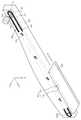
도 5는 도 3에 도시된 유기층 증착 장치의 척 이동부재와 가이드 부재를 나타내는 사시도이다. 도 6은 도 5의 A부분을 보여주는 측면도이다. 도 7은 도 6에 도시된 후크부의 작동을 보여주는 개념도이다.FIG. 5 is a perspective view illustrating the chuck moving member and the guide member of the organic layer deposition apparatus illustrated in FIG. 3. FIG. 6 is a side view illustrating portion A of FIG. 5. FIG. 7 is a conceptual view illustrating the operation of the hook unit illustrated in FIG. 6.
도 5 내지 도 7을 참고하면, 가이드 부재(221)의 외측면에는 체인부(260)가 배치될 수 있으며, 척 이동부재(230)에는 체인부(260)에 대응되도록 후크부(240)가 배치될 수 있다. 이때, 후크부(240)는 체인부(260)에 일부가 삽입되어 체인부(260)의 구동에 따라 척 이동부재(230)가 가이드 부재(221)를 따라 이동하게 된다.5 to 7, the
이에 대해 상술하면, 체인부(260)는 가이드 부재(221)에 회전 가능하도록 설치되는 스프로켓(261)을 포함할 수 있다. 또한, 체인부(260)는 스프로켓(261)의 외면을 감싸도록 설치되는 타이밍 체인(Timing chain)(262)을 포함할 수 있다. 이때, 타이밍 체인(262)은 가이드 부재(221)의 길이 방향으로 설치될 수 있다.In detail, the
이때, 스프로켓(261)은 타이밍 체인(262)의 일단에 설치되는 제1 스프로켓(261a)과, 타이밍 체인(262)의 타단에 설치되는 제2 스프로켓(261b)을 포함할 수 있다. 특히 제1 스프로켓(261a)과 제2 스프로켓(261b)은 타이밍 체인(262)이 회전할 때, 타이밍 체인(262)이 경로를 벗어나는 것을 방지할 수 있다.In this case, the
또한, 제1 스프로켓(261a)은 구동력을 전달받아 타이밍 체인(262)을 회전시킬 수 있다. 이때, 제2 스프로켓(261b)은 피동적으로 회전하여 타이밍 체인(262)이 회전할 때 함께 회전할 수 있다.In addition, the
한편, 체인부(260)는 스프로켓(261)과 연결되어 스프로켓(261)을 회전시키는 구동부(264)를 포함할 수 있다. 특히 구동부(264)는 스프로켓(261)과 회전축(265)을 통하여 연결될 수 있다. 구체적으로 구동부(264)는 제1 스프로켓(261a)과 회전축(265)을 통하여 연결될 수 있다.Meanwhile, the
이때, 구동부(264)는 제1 챔버(731)의 외측에 배치될 수 있다. 구체적으로 구동부(264)는 제1 챔버(731)의 외면에 설치되며, 회전축(265)은 제1 챔버(731)를 관통하도록 설치되어 제1 스프로켓(261a)과 연결될 수 있다.In this case, the driving
체인부(260)는 타이밍 체인(262)의 내부에 설치되어 타이밍 체인(262)이 자중에 의하여 늘어지는 것을 방지하는 텐션유지유닛(263)을 포함할 수 있다. 이때, 텐션유지유닛(263)은 복수개 구비되며, 복수개의 텐션유지유닛(263)은 서로 일정 간격 이격되도록 설치될 수 있다.The
특히 복수개의 텐션유지유닛(263)은 제1 스프로켓(261a)과 제2 스프로켓(261b) 사이에 설치될 수 있다. 또한, 복수개의 텐션유지유닛(263)은 스프로켓 형태로 형성되어 타이밍 체인(262)의 텐션을 유지시킬 수 있다.In particular, the plurality of
구체적으로 텐션유지유닛(263)은 타이밍 체인(262)의 하측 부분을 가력하여 타이밍 체인(262)의 텐션을 유지시킬 수 있다. 특히 텐션유지유닛(263)은 제1 스프로켓(261a)를 통과하여 하측으로 이동하는 타이밍 체인(262)와 접촉하여 가력할 수 있다.In detail, the
이때, 텐션유지유닛(263)은 복수개의 텐션유지스프로켓(미표기)을 구비할 수 있다. 특히 상기 복수개의 텐션유지스프로켓은 세개로 구성될 수 있으며, 두개는 상측에 배치되고 나머지 하나는 두개의 텐션유지스프로켓의 하측에 배치되어 타이밍 체인(262)와 접촉할 수 있다. 다만, 본 발명에서는 텐션유지스프로켓의 개수를 세개로 한정하여 설명하고 있으나 이는 본 발명의 일 실시예에 불과하고 본 발명은 상기에 제한되지 않으며 텐션유지유닛(263)이 타미이 체인(262)의 텐션(Tension)을 유지시키는 다양한 실시예로 변경 가능하다.At this time, the
한편, 후크부(240)는 척 이동부재(230)에 설치되는 후크하우징(241)을 포함할 수 있다. 이때, 후크하우징(241)은 척 이동부재(230)에 고정되도록 설치될 수 있다. 또한, 후크부(240)는 후크하우징(241)을 선형운동하도록 후크하우징(241)과 결합하는 후크(242)를 포함할 수 있다. 이때, 후크(242)는 체인부(260)와의 접촉에 따라 후크하우징(241)의 높이 방향을 선형 운동할 수 있다.On the other hand, the
후크부(240)는 후크하우징(241)과 후크에 설치되는 탄성부(243)를 포함할 수 있다. 이때, 탄성부(243)는 인장스프링 형태로 형성되어 후크(242)의 선형 운동 시 운동 방향의 반대 방향으로 복원력을 제공할 수 있다. 특히 탄성부(243)는 후크(242)가 후크하우징(241)의 상측 방향으로 이동할 때, 후크(242)의 운동 방향과 반대 방향으로 복원력을 제공할 수 있다. 또한, 탄성부(243)는 인장스프링 형태에 한정되는 것이 아니라 후크(242)에 복원력을 제공하는 모든 장치 및 모든 재질을 포함할 수 있다.The
척 이동부재(230)와 가이드 부재(221) 사이에는 LM 가이드(220)가 배치될 수 있다. LM 가이드(220)는 상기 가이드 부재(221)의 일면에 배치되는 한 쌍의 가이드 레일(223)과, 척 이동부재(230)의 일면에 배치되는 가이드 블록(225)으로 이루어지며, 가이드 레일(223)에 가이드 블록(225)이 끼워져서, 가이드 블록(225)이 가이드 레일(223)을 따라 왕복 운동하게 된다.An
여기서, 상기 가이드 레일(223)로써 LM 레일(linear motion rail)을 구비하고, 상기 가이드 블록(225)으로써 LM 블록(linear motion block)을 구비하여, 소정의 LM 시스템(linear motion system)을 구성할 수 있다. LM 시스템은 과거의 미끄럼 안내 시스템에 비하여 마찰 계수가 작고 위치 오차가 거의 발생하지 않아 위치 결정도가 매우 높은 이송 시스템이며, 본 명세서에서는 이와 같은 LM 시스템에 대하여서는 그 상세한 설명을 생략하도록 한다Here, the
도 5를 참조하여, 가이드 부재(221) 상에서 이동하는 척 이동부재(230)의 동작을 설명한다.5, the operation of the
척 이동부재(230)는 체인부(260)와 후크부(240)의 작동에 따라 가이드 부재(221)를 따라 이동한다. 상세하게는, 척 이동부재(230)는 외부의 구동부(264)의 작동에 따라 이동할 수있다.The
구체적으로 외부의 구동부(264)가 작동하게 되면, 구동부(264)는 회전축(265)을 회전시켜 제1 스프로켓(261a)을 회전시킬 수 있다. 이때, 제1 스프로켓(261a)에 결합된 타이밍 체인(262)이 회전하게 된다. 타이밍 체인(262)이 회전하는 경우 타이밍 체인(262)에 형성된 공간으로 후크(242)가 삽입될 수 있다.Specifically, when the
특히 후크(242)는 타이밍 체인(262)이 회전에 따라 타이밍 체인(262)의 연결 부분에 접촉되면, 후크하우징(241)의 상측으로 이동할 수 있다. 이때, 탄성부(243)는 후크(242)를 타이밍 체인(262) 측으로 가력할 수 있다.In particular, the
상기와 같이 이동하는 동안, 타이밍 체인(262)이 지속적으로 회전하게 되면, 후크(242)는 타이밍 체인(262)의 연결된 부분을 통과하게 되고, 타이밍 체인(262)의 공간에 위치하게 된다. 이때, 탄성부(243)에서 후크(242)를 가력하여 후크(242)는 타이밍 체인(262)의 공간으로 삽입될 수 있다.While moving as described above, if the
상기와 같이 후크(242)가 타이밍 체인(262)에 삽입되면, 타이밍 체인(262)의 회전에 따라 후크(242)는 타이밍 체인(262)의 이동방향으로 이동할 수 있다. 이때, 후크(242)와 연결된 척 이동부재(230)는 후크(242)와 함께 이동하게 된다. 특히 척 이동부재(230)는 가이드 부재(221)의 외측면을 따라 이동하게 된다. 이때, LM 가이드(220)는 척 이동부재(230)가 가이드 부재(221)를 선형 운동하도록 보조할 수 있다.When the
특히 상기와 같이 후크(242)가 타이밍 체인(262)와 이동하는 경우 척 이동부재(230)은 도 5의 Y방향의 반대방향으로 이동할 수 있다. 즉, 척 이동부재(230)는 도 5의 화살표 방향으로 이동할 수 있다.In particular, when the
따라서 척 이동부재(230)가 가이드 부재(221)를 일정한 속도로 선형 운동함으로써 척 이동부재(230)의 속도가 가변하여 발생하는 증착물질의 리플(Ripple) 현상을 최소화할 수 있다. 또한, 척 이동부재(230)가 가이드 부재(221)를 일정한 속도로 선형 운동함으로써 제품을 생산 시 발생하는 불량을 최소화할 수 있어 제품 제작 비용 및 제품 검사 비용 등을 저감시킬 수 있다.Therefore, the
도 8은 도 1의 유기층 증착 장치의 유기층 증착 어셈블리를 개략적으로 도시한 사시도이다. 도 9는 도 8의 유기층 증착 어셈블리의 개략적인 측단면도이다. 도 10은 도 8의 유기층 증착 어셈블리의 개략적인 평단면도이다.FIG. 8 is a schematic perspective view of an organic layer deposition assembly of the organic layer deposition apparatus of FIG. 1. 9 is a schematic side cross-sectional view of the organic layer deposition assembly of FIG. 8. 10 is a schematic plan cross-sectional view of the organic layer deposition assembly of FIG. 8.
도 8 내지 도 10를 참조하면, 본 발명의 일 실시예에 관한 유기층 증착 어셈블리(100)는 증착원(110), 증착원 노즐부(120), 차단판 어셈블리(130) 및 패터닝 슬릿 시트(150)를 포함한다.8 to 10, an organic
여기서, 도 8 내지 도 10에는 설명의 편의를 위해 챔버를 도시하지 않았지만, 도 8 내지 도 10의 모든 구성은 적절한 진공도가 유지되는 챔버 내에 배치되는 것이 바람직하다. 이는 증착 물질의 직진성을 확보하기 위함이다.Here, although the chamber is not shown in FIGS. 8 to 10 for convenience of description, all the components of FIGS. 8 to 10 are preferably disposed in a chamber in which an appropriate degree of vacuum is maintained. This is to ensure the straightness of the deposition material.
이러한 챔버 내에는 피 증착체인 기판(500)이 정전척(도 1의 600 참조)에 의해 이송된다. 상기 기판(500)은 평판 표시 장치용 기판이 될 수 있는데, 다수의 평판 표시 장치를 형성할 수 있는 마더 글라스(mother glass)와 같은 대면적 기판이 적용될 수 있다.In such a chamber, the
여기서, 본 발명의 일 실시예에서는, 기판(500)이 유기층 증착 어셈블리(100)에 대하여 상대적으로 이동하는데, 바람직하게는 유기층 증착 어셈블리(100)에 대하여 기판(500)이 화살표 A 방향으로 이동하도록 할 수 있다.Here, in one embodiment of the present invention, the
상세히, 기존 FMM 증착 방법에서는 마스크의 크기가 기판 크기와 동일하거나 이보다 커야 했다. 따라서, 기판 사이즈가 증가할수록 마스크도 대형화되어야 하며, 따라서 이러한 대형의 마스크의 제작이 용이하지 않고, 마스크를 인장하여 정밀한 패턴으로 얼라인(align) 하기도 용이하지 않다는 문제점이 존재하였다.In detail, the conventional FMM deposition method required the mask size to be equal to or larger than the substrate size. Therefore, as the substrate size increases, the mask also needs to be enlarged. Therefore, there is a problem that it is not easy to manufacture such a large mask, and it is not easy to align the mask in a precise pattern by tensioning the mask.
이와 같은 문제점을 해결하기 위하여, 본 발명의 일 실시예에 관한 유기층 증착 어셈블리(100)는, 유기층 증착 어셈블리(100)와 기판(500)이 서로 상대적으로 이동하면서 증착이 이루어지는 것을 일 특징으로 한다. 다시 말하면, 유기층 증착 어셈블리(100)와 마주보도록 배치된 기판(500)이 Y축 방향을 따라 이동하면서 연속적으로 증착을 수행하게 된다. 즉, 기판(500)이 도 3의 화살표 A 방향으로 이동하면서 스캐닝(scanning) 방식으로 증착이 수행되는 것이다. 여기서, 도면에는 기판(500)이 챔버(도 1의 731 참조) 내에서 Y축 방향으로 이동하면서 증착이 이루어지는 것으로 도시되어 있으나, 본 발명의 사상은 이에 제한되지 아니하며, 기판(500)은 고정되어 있고 유기층 증착 어셈블리(100) 자체가 Y축 방향으로 이동하면서 증착을 수행하는 것도 가능하다 할 것이다.In order to solve such a problem, the organic
따라서, 본 발명의 유기층 증착 어셈블리(100)에서는 종래의 FMM에 비하여 훨씬 작게 패터닝 슬릿 시트(150)를 만들 수 있다. 즉, 본 발명의 유기층 증착 어셈블리(100)의 경우, 기판(500)이 Y축 방향을 따라 이동하면서 연속적으로, 즉 스캐닝(scanning) 방식으로 증착을 수행하기 때문에, 패터닝 슬릿 시트(150)의 X축 방향으로의 폭과 기판(500)의 X축 방향으로의 폭만 실질적으로 동일하게 형성되면, 패터닝 슬릿 시트(150)의 Y축 방향의 길이는 기판(500)의 길이보다 훨씬 작게 형성되어도 무방하게 된다. 물론, 패터닝 슬릿 시트(150)의 X축 방향으로의 폭이 기판(500)의 X축 방향으로의 폭보다 작게 형성되더라도, 기판(500)과 유기층 증착 어셈블리(100)의 상대적 이동에 의한 스캐닝 방식에 의해 충분히 기판(500) 전체에 대하여 증착을 할 수 있게 된다.Thus, in the organic
이와 같이, 종래의 FMM에 비하여 훨씬 작게 패터닝 슬릿 시트(150)를 만들 수 있기 때문에, 본 발명의 패터닝 슬릿 시트(150)는 그 제조가 용이하다. 즉, 패터닝 슬릿 시트(150)의 에칭 작업이나, 그 이후의 정밀 인장 및 용접 작업, 이동 및 세정 작업 등 모든 공정에서, 작은 크기의 패터닝 슬릿 시트(150)가 FMM 증착 방법에 비해 유리하다. 또한, 이는 디스플레이 장치가 대형화될수록 더욱 유리하게 된다.Thus, since the
이와 같이, 유기층 증착 어셈블리(100)와 기판(500)이 서로 상대적으로 이동하면서 증착이 이루어지기 위해서는, 유기층 증착 어셈블리(100)와 기판(500)이 일정 정도 이격되는 것이 바람직하다. 이에 대하여는 뒤에서 상세히 기술하기로 한다.As such, in order for the deposition to be performed while the organic
한편, 챔버 내에서 상기 기판(500)과 대향하는 측에는, 증착 물질(115)이 수납 및 가열되는 증착원(110)이 배치된다.Meanwhile, the
상기 증착원(110)은 그 내부에 증착 물질(115)이 채워지는 도가니(111)와, 이 도가니(111)를 가열시키는 히터(112)가 구비된다.The
증착원(110)의 일 측, 상세하게는 증착원(110)에서 기판(500)을 향하는 측에는 증착원 노즐부(120)가 배치된다. 그리고, 증착원 노즐부(120)에는, X축 방향을 따라서 복수 개의 증착원 노즐(121)들이 형성된다. 여기서, 상기 복수 개의 증착원 노즐(121)들은 등 간격으로 형성될 수 있다. 증착원(110) 내에서 기화된 증착 물질(115)은 이와 같은 증착원 노즐부(120)의 증착원 노즐(121)들을 통과하여 피 증착체인 기판(500) 쪽으로 향하게 되는 것이다.The deposition
증착원 노즐부(120)의 일 측에는 차단판 어셈블리(130)가 구비된다. 상기 차단판 어셈블리(130)는 복수 개의 차단판(131)들과, 차단판(131)들 외측에 구비되는 차단판 프레임(132)을 포함한다. 상기 복수 개의 차단판(131)들은 X축 방향을 따라서 서로 나란하게 배치될 수 있다. 여기서, 상기 복수 개의 차단판(131)들은 등 간격으로 형성될 수 있다. 또한, 각각의 차단판(131)들은 도면에서 보았을 때 YZ평면을 따라 연장되어 있고, 바람직하게는 직사각형으로 구비될 수 있다. 이와 같이 배치된 복수 개의 차단판(131)들은 증착원 노즐부(120)와 패터닝 슬릿 시트(150) 사이의 공간을 복수 개의 증착 공간(S)으로 구획한다. 즉, 본 발명의 일 실시예에 관한 유기층 증착 어셈블리(100)는 상기 차단판(131)들에 의하여, 도 12에서 볼 수 있듯이, 증착 물질이 분사되는 각각의 증착원 노즐(121) 별로 증착 공간(S)이 분리된다.A blocking
여기서, 각각의 차단판(131)들은 서로 이웃하고 있는 증착원 노즐(121)들 사이에 배치될 수 있다. 이는 다시 말하면, 서로 이웃하고 있는 차단판(131)들 사이에 하나의 증착원 노즐(121)이 배치되는 것이다. 바람직하게, 증착원 노즐(121)은 서로 이웃하고 있는 차단판(131) 사이의 정 중앙에 위치할 수 있다. 그러나 본 발명은 반드시 이에 한정되지 않으며, 서로 이웃하고 있는 차단판(131)들 사이에 복수의 증착원 노즐(121)이 배치하여도 무방하다. 다만, 이 경우에도 복수의 증착원 노즐(121)들이 서로 이웃하고 있는 차단판(131) 사이의 정 중앙에 위치하도록 하는 것이 바람직하다.Here, each of the blocking
이와 같이, 차단판(131)이 증착원 노즐부(120)와 패터닝 슬릿 시트(150) 사이의 공간을 복수 개의 증착 공간(S)으로 구획함으로써, 하나의 증착원 노즐(121)로부터 배출되는 증착 물질은 다른 증착원 노즐(121)로부터 배출된 증착 물질들과 혼합되지 않고, 패터닝 슬릿(151)을 통과하여 기판(500)에 증착되는 것이다. 즉, 상기 차단판(131)들은 각 증착원 노즐(121)을 통해 배출되는 증착 물질이 분산되지 않고 Z축 방향으로 직진하도록 증착 물질의 이동 경로를 가이드 하는 역할을 수행한다.As described above, the blocking
이와 같이, 차단판(131)들을 구비하여 증착 물질의 직진성을 확보함으로써, 기판에 형성되는 음영(shadow)의 크기를 대폭적으로 줄일 수 있으며, 따라서 유기층 증착 어셈블리(100)와 기판(500)을 일정 정도 이격시키는 것이 가능해진다. 이에 대하여는 뒤에서 상세히 기술하기로 한다.As such, by providing the blocking
한편, 증착원(110)과 기판(500) 사이에는 패터닝 슬릿 시트(150) 및 프레임(155)이 더 구비된다. 상기 프레임(155)은 대략 창문 틀과 같은 형태로 형성되며, 그 내측에 패터닝 슬릿 시트(150)가 결합된다. 그리고, 패터닝 슬릿 시트(150)에는 X축 방향을 따라서 복수 개의 패터닝 슬릿(151)들이 형성된다. 각 패터닝 슬릿(151)들은 Y축 방향을 따라 연장되어 있다. 증착원(110) 내에서 기화되어 증착원 노즐(121)을 통과한 증착 물질(115)은 패터닝 슬릿(151)들을 통과하여 피 증착체인 기판(500) 쪽으로 향하게 된다.Meanwhile, a
상기 패터닝 슬릿 시트(150)는 금속 박판으로 형성되고, 인장된 상태에서 프레임(155)에 고정된다. 상기 패터닝 슬릿(151)은 스트라이프 타입(stripe type)으로 패터닝 슬릿 시트(150)에 에칭을 통해 형성된다. 여기서, 상기 패터닝 슬릿(151)의 개수는 기판(500)에 형성될 증착 패턴의 개수에 대응되도록 하는 것이 바람직하다.The
한편, 상술한 차단판 어셈블리(130)와 패터닝 슬릿 시트(150)는 서로 일정 정도 이격되도록 형성될 수 있으며, 차단판 어셈블리(130)와 패터닝 슬릿 시트(150)는 별도의 연결 부재(135)에 의하여 서로 연결될 수 있다.Meanwhile, the above-described
상술한 바와 같이, 본 발명의 일 실시예에 관한 유기층 증착 어셈블리(100)는 기판(500)에 대하여 상대적으로 이동하면서 증착을 수행하며, 이와 같이 유기층 증착 어셈블리(100)가 기판(500)에 대하여 상대적으로 이동하기 위해서 패터닝 슬릿 시트(150)는 기판(500)으로부터 일정 정도 이격되도록 형성된다. 그리고, 패터닝 슬릿 시트(150)와 기판(500)을 이격시킬 경우 발생하는 음영(shadow) 문제를 해결하기 위하여, 증착원 노즐부(120)와 패터닝 슬릿 시트(150) 사이에 차단판(131)들을 구비하여 증착 물질의 직진성을 확보함으로써, 기판에 형성되는 음영(shadow)의 크기를 대폭적으로 감소시킨 것이다.As described above, the organic
종래의 FMM 증착 방법에서는 기판에 음영(shadow)이 생기지 않도록 하기 위하여 기판에 마스크를 밀착시켜서 증착 공정을 진행하였다. 그러나, 이와 같이 기판에 마스크를 밀착시킬 경우, 기판과 마스크 간의 접촉에 의해 기판에 이미 형성되어 있던 패턴들이 긁히는 등 불량 문제가 발생한다는 문제점이 존재하였다. 또한, 마스크를 기판에 대하여 이동시킬 수 없기 때문에, 마스크가 기판과 동일한 크기로 형성되어야 한다. 따라서, 디스플레이 장치가 대형화됨에 따라 마스크의 크기도 커져야 하는데, 이와 같은 대형 마스크를 형성하는 것이 용이하지 아니하다는 문제점이 존재하였다.In the conventional FMM deposition method, the deposition process was performed by bringing a mask into close contact with the substrate in order to prevent shadows on the substrate. However, when the mask is in close contact with the substrate in this manner, there is a problem that a defect problem occurs such that the patterns already formed on the substrate are scratched by the contact between the substrate and the mask. Also, since the mask cannot be moved relative to the substrate, the mask must be formed to the same size as the substrate. Therefore, as the display device is enlarged, the size of the mask must be increased, but there is a problem that it is not easy to form such a large mask.
이와 같은 문제점을 해결하기 위하여, 본 발명의 일 실시예에 관한 유기층 증착 어셈블리(100)에서는 패터닝 슬릿 시트(150)가 피 증착체인 기판(500)과 소정 간격을 두고 이격되도록 배치되도록 한다. 이것은 차단판(131)을 구비하여, 기판(500)에 생성되는 음영(shadow)이 작아지게 됨으로써 실현 가능해진다.In order to solve such a problem, in the organic
또한, 본 발명에 의해서 마스크를 기판보다 작게 형성한 후, 마스크를 기판에 대하여 이동시키면서 증착을 수행할 수 있게 됨으로써, 마스크 제작이 용이해지는 효과를 얻을 수 있다. 또한, 기판과 마스크 간의 접촉에 의한 불량을 방지하는 효과를 얻을 수 있다. 또한, 공정에서 기판과 마스크를 밀착시키는 시간이 불필요해지기 때문에, 제조 속도가 향상되는 효과를 얻을 수 있다.In addition, by forming the mask smaller than the substrate according to the present invention, it is possible to perform the deposition while moving the mask with respect to the substrate, it is possible to obtain the effect that the mask fabrication becomes easy. In addition, the effect of preventing a defect due to contact between the substrate and the mask can be obtained. In addition, since the time for bringing the substrate into close contact with the mask is unnecessary in the step, an effect of increasing the manufacturing speed can be obtained.
또한, 유기층 증착 어셈블리(1100)를 구성하는 증착원(110), 증착원 노즐부(120) 및 패터닝 슬릿 시트(150)가 일체로 형성되는 것이 아니라, 증착부(730) 내에 각각 별도의 부재로 형성된다. 이와 같은 구성에 의해, 증착 물질(115) 충전을 위한 증착원(110)의 인입 및 인출, 세정 또는 교체를 위한 패터닝 슬릿 시트(150)의 인입 및 인출 등이 용이하게 수행되는 효과를 얻을 수 있다.In addition, the
도 11은 본 발명의 다른 일 실시예에 관한 유기층 증착 어셈블리를 개략적으로 도시한 사시도이다.11 is a perspective view schematically showing an organic layer deposition assembly according to another embodiment of the present invention.
도 11을 참고하면, 유기층 증착 어셈블리(800)는 증착원(810), 증착원 노즐부(820), 제1 차단판 어셈블리(830), 제2 차단판 어셈블리(840), 패터닝 슬릿 시트(850)를 포함한다. 여기서, 증착원(810), 제1 차단판 어셈블리(830) 및 패터닝 슬릿 시트(850)의 상세한 구성은 전술한 도 3에 따른 실시예와 동일하므로 상세한 설명을 생략한다. 본 실시예에서는 제1 차단판 어셈블리(830)의 일 측에 제2 차단판 어셈블리(840)가 구비된다는 점에서 전술한 실시예와 구별된다.Referring to FIG. 11, the organic
상세히, 상기 제2 차단판 어셈블리(840)는 복수 개의 제2 차단판(841)들과, 제2 차단판(841)들 외측에 구비되는 제2 차단판 프레임(842)을 포함한다. 상기 복수 개의 제2 차단판(841)들은 X축 방향을 따라서 서로 나란하게 구비될 수 있다. 그리고, 상기 복수 개의 제2 차단판(841)들은 등 간격으로 형성될 수 있다. 또한, 각각의 제2 차단판(841)은 도면에서 보았을 때 YZ평면과 나란하도록, 다시 말하면 X축 방향에 수직이 되도록 형성된다.In detail, the second blocking plate assembly 840 includes a plurality of second blocking plates 841 and a second
이와 같이 배치된 복수 개의 제1 차단판(831) 및 제2 차단판(841)들은 증착원 노즐부(820)과 패터닝 슬릿 시트(850) 사이의 공간을 구획하는 역할을 수행한다. 즉, 상기 제1 차단판(831) 및 제2 차단판(841)에 의하여, 증착 물질이 분사되는 각각의 증착원 노즐(821) 별로 증착 공간이 분리되는 것을 일 특징으로 한다.The plurality of
여기서, 각각의 제2 차단판(841)들은 각각의 제1 차단판(831)들과 일대일 대응하도록 배치될 수 있다. 다시 말하면, 각각의 제2 차단판(841)들은 각각의 제1 차단판(831)들과 얼라인(align) 되어 서로 나란하게 배치될 수 있다. 즉, 서로 대응하는 제1 차단판(831)과 제2 차단판(841)은 서로 동일한 평면상에 위치하게 되는 것이다. 도면에는, 제1 차단판(831)의 길이와 제2 차단판(841)의 X축 방향의 폭이 동일한 것으로 도시되어 있지만, 본 발명의 사상은 이에 제한되지 아니한다. 즉, 패터닝 슬릿(851)과의 정밀한 얼라인(align)이 요구되는 제2 차단판(841)은 상대적으로 얇게 형성되는 반면, 정밀한 얼라인이 요구되지 않는 제1 차단판(831)은 상대적으로 두껍게 형성되어, 그 제조가 용이하도록 하는 것도 가능하다 할 것이다.Here, each of the second blocking plates 841 may be disposed to correspond one-to-one with each of the
도 12는 본 발명의 또 다른 일 실시예에 따른 유기층 증착 어셈블리를 개략적으로 도시한 사시도이다.12 is a perspective view schematically showing an organic layer deposition assembly according to another embodiment of the present invention.
도 12를 참고하면, 본 발명의 또 다른 일 실시예에 따른 유기층 증착 어셈블리(900)는 증착원(910), 증착원 노즐부(920) 및 패터닝 슬릿 시트(950)를 포함한다.Referring to FIG. 12, the organic
여기서, 증착원(910)은 그 내부에 증착 물질(915)이 채워지는 도가니(911)와, 도가니(911)를 가열시켜 도가니(911) 내부에 채워진 증착 물질(915)을 증착원 노즐부(920) 측으로 증발시키기 위한 히터(912)를 포함한다. 한편, 증착원(910)의 일 측에는 증착원 노즐부(920)가 배치되고, 증착원 노즐부(920)에는 Y축 방향을 따라서 복수 개의 증착원 노즐(921)들이 형성된다. 한편, 증착원(910)과 기판(500) 사이에는 패터닝 슬릿 시트(950) 및 프레임(955)이 더 구비되고, 패터닝 슬릿 시트(950)에는 X축 방향을 따라서 복수 개의 패터닝 슬릿(951)들 및 스페이서(952)들이 형성된다. 그리고, 증착원(910) 및 증착원 노즐부(920)와 패터닝 슬릿 시트(950)는 연결 부재(935)에 의해서 결합된다.Here, the
본 실시예는 전술한 실시예들에 비하여 증착원 노즐부(920)에 구비된 복수 개의 증착원 노즐(921)들의 배치가 상이한바, 이에 대하여 상세히 설명한다.In the present embodiment, the arrangement of the plurality of
증착원(910)의 일 측, 상세하게는 증착원(910)에서 기판(500)을 향하는 측에는 증착원 노즐부(920)가 배치된다. 그리고, 증착원 노즐부(920)에는, Y축 방향 즉 기판(500)의 스캔 방향을 따라서 복수 개의 증착원 노즐(921)들이 형성된다. 여기서, 상기 복수 개의 증착원 노즐(921)들은 등 간격으로 형성될 수 있다. 증착원(910) 내에서 기화된 증착 물질(915)은 이와 같은 증착원 노즐부(920)를 통과하여 피 증착체인 기판(500) 쪽으로 향하게 되는 것이다. 이와 같이, 증착원 노즐부(920) 상에 Y축 방향 즉 기판(500)의 스캔 방향을 따라서 복수 개의 증착원 노즐(921)들이 형성할 경우, 패터닝 슬릿 시트(950)의 각각의 패터닝 슬릿(951)들을 통과하는 증착 물질에 의해 형성되는 패턴의 크기는 증착원 노즐(921) 하나의 크기에만 영향을 받으므로(즉, X축 방향으로는 증착원 노즐(921)이 하나만 존재하는 것에 다름 아니므로), 음영(shadow)이 발생하지 않게 된다. 또한, 다수 개의 증착원 노즐(921)들이 스캔 방향으로 존재하므로, 개별 증착원 노즐 간 플럭스(flux) 차이가 발생하여도 그 차이가 상쇄되어 증착 균일도가 일정하게 유지되는 효과를 얻을 수 있다. 더불어, 도 10등에 도시된 실시예에 구비된 차단판 어셈블리가 구비되지 아니하기 때문에, 차단판 어셈블리에 증착 물질이 증착되지 않게 되어, 증착 물질의 이용 효율이 향상되는 효과를 얻을 수 있다.The deposition
도 13은 본 발명의 유기층 증착 장치를 이용하여 제조된 액티브 매트릭스형 유기 발광 디스플레이 장치의 단면을 도시한 것이다.13 is a cross-sectional view of an active matrix organic light emitting display device manufactured using the organic layer deposition apparatus of the present invention.
도 13을 참고하면, 상기 액티브 매트리스형의 유기 발광 디스플레이 장치(10)는 기판(500) 상에 형성된다. 상기 기판(500)은 투명한 소재, 예컨대 글래스재, 플라스틱재, 또는 금속재로 형성될 수 있다. 상기 기판(500)상에는 전체적으로 버퍼층과 같은 절연막(31)이 형성되어 있다.Referring to FIG. 13, the active mattress organic light emitting
상기 절연막(31) 상에는 도 13에서 볼 수 있는 바와 같은 TFT(40)와, 커패시터(50)와, 유기 발광 소자(60)가 형성된다.On the insulating
상기 절연막(31)의 윗면에는 소정 패턴으로 배열된 반도체 활성층(41)이 형성되어 있다. 상기 반도체 활성층(41)은 게이트 절연막(32)에 의하여 매립되어 있다. 상기 활성층(41)은 p형 또는 n형의 반도체로 구비될 수 있다.The semiconductor
상기 게이트 절연막(32)의 윗면에는 상기 활성층(41)과 대응되는 곳에 TFT(40)의 게이트 전극(42)이 형성된다. 그리고, 상기 게이트 전극(42)을 덮도록 층간 절연막(33)이 형성된다. 상기 층간 절연막(33)이 형성된 다음에는 드라이 에칭 등의 식각 공정에 의하여 상기 게이트 절연막(32)과 층간 절연막(33)을 식각하여 콘택 홀을 형성시켜서, 상기 활성층(41)의 일부를 드러나게 한다.The
그 다음으로, 상기 층간 절연막(33) 상에 소스/드레인 전극(43)이 형성되는 데, 콘택 홀을 통해 노출된 활성층(41)에 접촉되도록 형성된다. 상기 소스/드레인 전극(43)을 덮도록 보호막(34)이 형성되고, 식각 공정을 통하여 상기 드레인 전극(43)의 일부가 드러나도록 한다. 상기 보호막(34) 위로는 보호막(34)의 평탄화를 위해 별도의 절연막을 더 형성할 수도 있다.Next, a source /
한편, 상기 유기 발광 소자(60)는 전류의 흐름에 따라 적,녹,청색의 빛을 발광하여 소정의 화상 정보를 표시하기 위한 것으로서, 상기 보호막(34) 상에 제1 전극(61)을 형성한다. 상기 제1 전극(61)은 TFT(40)의 드레인 전극(43)과 전기적으로 연결된다.On the other hand, the organic
그리고, 상기 제1 전극(61)을 덮도록 화소 정의막(35)이 형성된다. 이 화소 정의막(35)에 소정의 개구를 형성한 후, 이 개구로 한정된 영역 내에 발광층을 포함하는 유기층(63)을 형성한다. 그리고 유기층(63) 위로는 제2 전극(62)을 형성한다.The
상기 화소 정의막(35)은 각 화소를 구획하는 것으로, 유기물로 형성되어, 제1 전극(61)이 형성되어 있는 기판의 표면, 특히, 보호층(34)의 표면을 평탄화한다.The
상기 제1 전극(61)과 제2 전극(62)은 서로 절연되어 있으며, 발광층을 포함하는 유기층(63)에 서로 다른 극성의 전압을 가해 발광이 이뤄지도록 한다.The
상기 발광층을 포함하는 유기층(63)은 저분자 또는 고분자 유기물이 사용될 수 있는 데, 저분자 유기물을 사용할 경우 홀 주입층(HIL: Hole Injection Layer), 홀 수송층(HTL: Hole Transport Layer), 발광층(EML: Emission Layer), 전자 수송층(ETL: Electron Transport Layer), 전자 주입층(EIL: Electron Injection Layer) 등이 단일 혹은 복합의 구조로 적층되어 형성될 수 있으며, 사용 가능한 유기 재료도 구리 프탈로시아닌(CuPc: copper phthalocyanine), N,N-디(나프탈렌-1-일)-N,N'-디페닐-벤지딘 (N,N'-Di(naphthalene-1-yl)-N,N'-diphenyl-benzidine: NPB) , 트리스-8-하이드록시퀴놀린 알루미늄(tris-8-hydroxyquinoline aluminum)(Alq3) 등을 비롯해 다양하게 적용 가능하다.The
이러한 유기 발광막을 형성한 후에는 제2 전극(62)을 역시 동일한 증착 공정으로 형성할 수 있다.After the organic light emitting film is formed, the
한편, 상기 제1 전극(61)은 애노드 전극의 기능을 하고, 상기 제2 전극(62)은 캐소드 전극의 기능을 할 수 있는 데, 물론, 이들 제1 전극(61)과 제2 전극(62)의 극성은 반대로 되어도 무방하다. 그리고, 제1 전극(61)은 각 화소의 영역에 대응되도록 패터닝될 수 있고, 제2 전극(62)은 모든 화소를 덮도록 형성될 수 있다.Meanwhile, the
상기 제1 전극(61)은 투명 전극 또는 반사형 전극으로 구비될 수 있는 데, 투명전극으로 사용될 때에는 ITO, IZO, ZnO, 또는 In2O3로 구비될 수 있고, 반사형 전극으로 사용될 때에는 Ag, Mg, Al, Pt, Pd, Au, Ni, Nd, Ir, Cr, 및 이들의 화합물 등으로 반사층을 형성한 후, 그 위에 ITO, IZO, ZnO, 또는 In2O3로 투명전극층을 형성할 수 있다. 이러한 제1 전극(61)은 스퍼터링 방법 등에 의해 성막된 후, 포토 리소그래피법 등에 의해 패터닝된다.The
한편, 상기 제2 전극(62)도 투명 전극 또는 반사형 전극으로 구비될 수 있는 데, 투명전극으로 사용될 때에는 이 제2 전극(62)이 캐소오드 전극으로 사용되므로, 일함수가 작은 금속 즉, Li, Ca, LiF/Ca, LiF/Al, Al, Ag, Mg, 및 이들의 화합물이 발광층을 포함하는 유기층(63)의 방향을 향하도록 증착한 후, 그 위에 ITO, IZO, ZnO, 또는 In2O3 등으로 보조 전극층이나 버스 전극 라인을 형성할 수 있다. 그리고, 반사형 전극으로 사용될 때에는 위 Li, Ca, LiF/Ca, LiF/Al, Al, Ag, Mg, 및 이들의 화합물을 전면 증착하여 형성한다. 이때, 증착은 전술한 발광층을 포함하는 유기층(63)의 경우와 마찬가지의 방법으로 행할 수 있다.Meanwhile, the
본 발명은 이 외에도, 유기 TFT의 유기층 또는 무기막 등의 증착에도 사용할 수 있으며, 기타, 다양한 소재의 성막 공정에 적용 가능하다.In addition to the above, the present invention can also be used for deposition of an organic layer or an inorganic film of an organic TFT, and can be applied to a film forming process of various other materials.
도 14는 유기층 증착 장치에서 패터닝 슬릿 시트에 패터닝 슬릿들이 등 간격으로 형성되어 있는 모습을 나타내는 도면이고, 도 15는 도 14의 패터닝 슬릿 시트를 이용하여 기판상에 형성된 유기층을 나타내는 도면이다.FIG. 14 is a view illustrating patterning slits formed at equal intervals in a patterning slit sheet in an organic layer deposition apparatus, and FIG. 15 is a view illustrating an organic layer formed on a substrate using the patterning slit sheet of FIG. 14.
도 14 및 도 15를 참고하면, 도 14 및 도 15에는 패터닝 슬릿(151)이 등간격으로 배치된 패터닝 슬릿 시트(150)가 도시되어 있다. 즉, 도 14에서 l1 = l2 = l3 = l4의 관계가 성립한다.14 and 15, a
이 경우, 중심선(C)을 지나는 증착 물질의 입사 각도는 기판(500)에 거의 수직이 된다. 따라서, 따라서 패터닝 슬릿(151a)을 통과한 증착 물질에 의하여 형성되는 유기층(P1)은 그 음영(shadow)의 크기는 최소가 되며, 우측 음영(SR1)과 좌측 음영(SL1)이 대칭을 이루도록 형성된다.In this case, the angle of incidence of the deposition material passing through the center line C is substantially perpendicular to the
그러나, 중심선(C)으로부터 멀리 배치된 패터닝 슬릿을 지나는 증착 물질의 임계 입사 각도(θ)는 점점 커지게 되어서, 가장 끝 부분의 패터닝 슬릿(151e)을 지나는 증착 물질의 임계 입사 각도(θ)는 약 55°가 될 수 있다. 따라서, 증착 물질이 패터닝 슬릿(151e)에 대해 기울어져서 입사하게 되고, 패터닝 슬릿(151e)을 통과한 증착 물질에 의하여 형성된 유기층(P5)은 그 음영(shadow)의 크기가 최대가 되며, 특히 좌측 음영(SR5)이 우측 음영(SR5)보다 더 길게 형성된다.However, the critical incidence angle θ of the deposition material passing through the patterning slit disposed away from the centerline C becomes larger and larger, so that the critical incidence angle θ of the deposition material passing through the
즉, 증착 물질의 임계 입사 각도(θ)가 커짐에 따라 음영(shadow)의 크기도 커지게 되며, 특히 중심선(C)로부터 먼 쪽의 음영(shadow)의 크기가 커지게 된다. 그리고, 증착 물질의 임계 입사 각도(θ)는 중심부로부터 패터닝 슬릿까지의 거리가 멀수록 커지게 된다. 따라서, 중심선(C)으로부터 패터닝 슬릿까지의 거리가 먼 유기층일수록 음영(shadow)의 크기가 커지게 되며, 특히 유기층의 양단부의 음영(shadow) 중 증착 공간(S)의 중심선(C)으로부터 먼 쪽의 음영(shadow)의 크기가 더 커지게 되는 것이다.That is, as the critical incidence angle θ of the deposition material increases, the size of the shadow increases, in particular, the size of the shadow far from the center line C increases. The critical incidence angle [theta] of the deposition material becomes larger as the distance from the center portion to the patterning slit is greater. Therefore, the larger the distance from the center line C to the patterning slit, the larger the size of the shadow, and in particular, the farther from the center line C of the deposition space S among the shadows at both ends of the organic layer. The size of the shadow will be larger.
즉, 도 15에서 보았을 때, 중심선(C)을 기준으로 왼쪽에 형성된 유기층들은 좌측 빗변이 우측 빗변보다 더 길도록 형성되며, 중심선(C)을 기준으로 오른쪽에 형성된 유기층들은 우측 빗변이 좌측 빗변보다 더 길도록 형성된다.That is, as shown in FIG. 15, the organic layers formed on the left side based on the center line C are formed so that the left hypotenuse is longer than the right hypotenuse, and the organic layers formed on the right side based on the center line C have the right hypotenuse than the left hypotenuse. It is formed longer.
또한, 중심선(C)을 기준으로 왼쪽에 형성된 유기층들은, 왼쪽에 형성된 유기층일수록 좌측 빗변의 길이가 더 길게 형성되며, 중심선(C)을 기준으로 오른쪽에 형성된 유기층들은, 오른쪽에 형성된 유기층일수록 우측 빗변의 길이가 더 길게 형성된다. 그리고, 결과적으로 증착 공간(S) 내에 형성된 유기층들은 중심선을 기준으로 대칭을 이루도록 형성될 수 있다.In addition, the organic layers formed on the left side based on the center line C have a longer length of the left hypotenuse as the organic layer formed on the left side, and the organic layers formed on the right side based on the center line C have a right hypotenuse as the organic layer formed on the right side. The length of is formed longer. As a result, the organic layers formed in the deposition space S may be formed to be symmetrical with respect to the center line.
이를 더욱 상세히 설명하면 다음과 같다.This will be described in more detail as follows.
패터닝 슬릿(151b)을 통과하는 증착 물질들은 θb의 임계 입사각으로 패터닝 슬릿(151b)을 통과하게 되고, 이 경우 패터닝 슬릿(151b)을 통과한 증착 물질에 의하여 형성된 유기층(P2)의 좌측 음영(shadow)은 SL2의 크기로 형성된다. 마찬가지로, 패터닝 슬릿(151c)을 통과하는 증착 물질들은 θc의 임계 입사각으로 패터닝 슬릿(151c)을 통과하게 되고, 이 경우 패터닝 슬릿(151c)을 통과한 증착 물질에 의하여 형성된 유기층(P3)의 좌측 음영(shadow)은 SL3의 크기로 형성된다. 마찬가지로, 패터닝 슬릿(151d)을 통과하는 증착 물질들은 θd의 임계 입사각으로 패터닝 슬릿(151d)을 통과하게 되고, 이 경우 패터닝 슬릿(151d)을 통과한 증착 물질에 의하여 형성된 유기층(P4)의 좌측 음영(shadow)은 SL4의 크기로 형성된다. 마지막으로, 패터닝 슬릿(151e)을 통과하는 증착 물질들은 θe의 임계 입사각으로 패터닝 슬릿(151e)을 통과하게 되고, 이 경우 패터닝 슬릿(151e)을 통과한 증착 물질에 의하여 형성된 유기층(P5)의 좌측 음영(shadow)은 SL5의 크기로 형성된다.The deposition materials passing through the
여기서, θb < θc < θd <θe 의 관계가 성립하므로, 각각의 패터닝 슬릿들을 통과한 유기층들의 음영(shadow) 크기 사이에는, SL1 < SL2 < SL3 < SL4 < SL5 의 관계가 성립하게 된다.Here, since the relationship of θb <θc <θd <θe holds, between the shadow sizes of the organic layers passing through the respective patterning slits, SL1 <SL2 <SL3 <SL4 <SL5 Relationship is established.
본 명세서에서는 본 발명을 한정된 실시예를 중심으로 설명하였으나, 본 발명의 범위 내에서 다양한 실시예가 가능하다. 또한 설명되지는 않았으나, 균등한 수단도 또한 본 발명에 그대로 결합되는 것이라 할 것이다. 따라서 본 발명의 진정한 보호범위는 아래의 특허청구범위에 의하여 정해져야 할 것이다.In the present specification, the present invention has been described with reference to limited embodiments, but various embodiments are possible within the scope of the present invention. In addition, although not described, equivalent means will also be referred to as incorporated in the present invention. Therefore, the true scope of the present invention will be defined by the claims below.
100: 유기층 증착 어셈블리110: 증착원
120: 증착원 노즐부130: 차단판 어셈블리
150: 패터닝 슬릿 시트151: 패터닝 슬릿
500: 기판100: organic layer deposition assembly 110: deposition source
120: deposition source nozzle unit 130: blocking plate assembly
150: patterning slit sheet 151: patterning slit
500: substrate
Claims (30)
Translated fromKorean증착 물질을 방사하는 증착원;
상기 증착원의 일 측에 배치되며, 복수 개의 증착원 노즐들이 형성되는 증착원 노즐부;
상기 증착원 노즐부와 대향되게 배치되고, 복수 개의 패터닝 슬릿들이 형성되는 패터닝 슬릿 시트;
상기 기판을 탈부착할 수 있는 정전척;
상기 정전척과 결합하여 상기 정전척을 이동시킬 수 있는 척 이동부재; 및
상기 척 이동부재의 이동 방향을 가이드하는 가이드 부재; 를 구비하고,
상기 척 이동부재는 높이가 가변하는 후크부를 갖고, 상기 가이드 부재는 상기 후크부에 대응하여 체인부를 가지며,
상기 후크부가 상기 체인부에 삽입되어 상기 체인부의 작동에 따라 상기 척 이동부재가 상기 가이드 부재를 따라 이동하고,
상기 기판은 상기 패터닝 슬릿 시트와 소정 정도 이격되도록 형성되어 상기 유기층 증착 장치에 대하여 상대적으로 이동가능하도록 형성되는 것을 특징으로 하는 유기층 증착 장치.In the organic layer deposition apparatus which forms an organic layer on a board | substrate,
A deposition source for emitting a deposition material;
A deposition source nozzle unit disposed on one side of the deposition source and having a plurality of deposition source nozzles formed therein;
A patterning slit sheet disposed to face the deposition source nozzle unit and having a plurality of patterning slits formed thereon;
An electrostatic chuck that can attach and detach the substrate;
A chuck moving member coupled to the electrostatic chuck to move the electrostatic chuck; And
A guide member for guiding a moving direction of the chuck moving member; And
The chuck moving member has a hook portion having a variable height, the guide member has a chain portion corresponding to the hook portion,
The hook portion is inserted into the chain portion and the chuck moving member moves along the guide member in accordance with the operation of the chain portion,
And the substrate is formed to be spaced apart from the patterned slit sheet by a predetermined degree so as to be movable relative to the organic layer deposition apparatus.
상기 체인부는,
상기 가이드 부재에 회전 가능하도록 설치되는 스프로켓;
상기 스프로켓의 외면을 감싸도록 설치되는 타이밍 체인;을 포함하는 것을 특징으로 하는 유기층 증착 장치.The method of claim 1,
The chain portion,
A sprocket rotatably installed on the guide member;
And a timing chain installed to surround the outer surface of the sprocket.
상기 스프로켓은,
상기 타이밍 체인의 일단에 설치되는 제1 스프로켓; 및
상기 타이밍 체인의 타단에 설치되는 제2 스프로켓;을 구비하는 것을 특징으로 하는 유기층 증착 장치.The method of claim 2,
The sprocket,
A first sprocket installed at one end of the timing chain; And
And a second sprocket installed at the other end of the timing chain.
상기 체인부는,
상기 타이밍 체인의 내부에 설치되어 상기 타이밍 체인의 텐션(Tension)을 유지시키는 텐션유지유닛;을 더 포함하는 것을 특징으로 하는 유기층 증착 장치.The method of claim 2,
The chain portion,
And a tension holding unit installed inside the timing chain to maintain tension of the timing chain.
상기 타이밍 체인은 상기 가이드 부재의 길이 방향으로 설치되는 것을 특징으로 하는 유기층 증착 장치.The method of claim 2,
And the timing chain is installed in the longitudinal direction of the guide member.
상기 체인부는,
상기 스프로켓과 연결되어 상기 스프로켓을 회전시키는 구동부;를 더 구비하는 것을 특징으로 하는 유기층 증착 장치.The method of claim 2,
The chain portion,
And a driving part connected to the sprocket to rotate the sprocket.
상기 증착원, 상기 증착원 노즐부, 상기 패터닝 슬릿 시트, 상기 정전척, 상기 척 이동부재 및 상기 가이드 부재가 내부에 설치되는 챔버;를 더 포함하고,
상기 구동부는 상기 챔버의 외부에 설치되어 상기 스프로켓과 샤프트로 연결되는 것을 특징으로 하는 유기층 증착 장치.The method of claim 6,
And a chamber in which the deposition source, the deposition source nozzle unit, the patterning slit sheet, the electrostatic chuck, the chuck moving member, and the guide member are installed therein.
The driving unit is installed on the outside of the chamber organic layer deposition apparatus, characterized in that connected to the sprocket and the shaft.
상기 후크부는,
상기 척 이동부재에 설치되는 후크하우징;
상기 후크하우징을 선형 운동하도록 상기 후크하우징과 결합하는 후크; 및
상기 후크하우징과 상기 후크에 설치되는 탄성부;를 구비하는 것을 특징으로 하는 유기층 증착 장치.The method of claim 1,
The hook portion,
A hook housing installed at the chuck moving member;
A hook that engages with the hook housing to linearly move the hook housing; And
And the hook housing and an elastic part installed on the hook.
상기 후크는 상기 체인부와의 접촉에 따라 상기 후크하우징의 높이 방향으로 선형 운동하는 것을 특징으로 하는 유기층 증착 장치.The method of claim 8,
And the hook linearly moves in the height direction of the hook housing according to the contact with the chain part.
상기 척 이동부재와 상기 가이드 부재 사이에 LM(Linear motion) 가이드를 더 구비하는 것을 특징으로 하는 유기층 증착 장치.The method of claim 1,
The organic layer deposition apparatus further comprises a linear motion (LM) guide between the chuck moving member and the guide member.
상기 LM 가이드는,
상기 척 이동부재 상에 배치되는 가이드 블록;
상기 가이드 부재 상에 배치되는 가이드 레일; 을 포함하며,
상기 가이드 블록은 상기 가이드 레일을 따라 이동하는 것을 특징으로 하는 유기층 증착 장치.The method of claim 10,
The LM guide,
A guide block disposed on the chuck moving member;
A guide rail disposed on the guide member; Including;
And the guide block moves along the guide rail.
상기 기판을 정전척으로 고정시키는 로딩부; 및
상기 정전척으로부터 증착이 완료된 상기 기판을 분리시키는 언로딩부;를 더 포함하는 것을 특징으로 하는 유기층 증착 장치.The method of claim 1,
A loading unit fixing the substrate with an electrostatic chuck; And
And an unloading part which separates the substrate from which the deposition is completed from the electrostatic chuck.
상기 후크부와 상기 체인부는 상기 정전척 및 상기 척 이동부재를 로딩부, 증착부 및 언로딩부로 순차적으로 이동시키는 것을 특징으로 하는 유기층 증착 장치.The method of claim 12,
And the hook part and the chain part sequentially move the electrostatic chuck and the chuck moving member to a loading part, a deposition part, and an unloading part.
상기 증착원에서 방시된 상기 증착 물질은 상기 패터닝 슬릿 시트를 통과하여 상기 기판 상에 패턴을 형성하면서 증착되는 것을 특징으로 하는 유기층 증착 장치.The method of claim 1,
And depositing a pattern formed on the substrate by passing the patterned slit sheet through the patterned slit sheet.
상기 유기층 증착 장치의 상기 패터닝 슬릿 시트는 상기 기판보다 작게 형성되는 것을 특징으로 하는 유기층 증착 장치.The method of claim 1,
And the patterning slit sheet of the organic layer deposition apparatus is formed smaller than the substrate.
상기 증착원 노즐부에는 제1 방향을 따라 복수 개의 증착원 노즐들이 형성되고,
상기 패터닝 슬릿 시트에는 상기 제1 방향에 대해 수직인 제2 방향을 따라 복수 개의 패터닝 슬릿들이 형성되는 것을 특징으로 하는 유기층 증착 장치.The method of claim 1,
A plurality of deposition source nozzles are formed in the deposition source nozzle part along a first direction,
And a plurality of patterning slits formed in the patterning slit sheet along a second direction perpendicular to the first direction.
상기 정전척을 척 이동부재에 결합하는 단계;
상기 척 이동부재는 가이드 부재를 따라 상기 정전척을 챔버 내로 이동하는 단계; 및
상기 챔버 내에 배치된 유기층 증착 어셈블리와의 상대적인 이동에 의해 상기 기판 상에 유기층을 증착하는 단계; 를 구비하며,
상기 척 이동부재는 체인부와 후크부가 서로 연동하여 상기 가이드 부재를 따라 이동하며,
상기 기판은 상기 유기층 증착 어셈블리와 이격되는 것을 특징으로 하는 유기 발광 표시 장치의 제조 방법.Securing the substrate to the electrostatic chuck;
Coupling the electrostatic chuck to a chuck moving member;
The chuck moving member moving the electrostatic chuck into a chamber along a guide member; And
Depositing an organic layer on the substrate by relative movement with an organic layer deposition assembly disposed within the chamber; Equipped with,
The chuck moving member is moved along the guide member in conjunction with the chain portion and the hook portion,
And the substrate is spaced apart from the organic layer deposition assembly.
상기 척 이동부재는 높이가 가변하는 후크부를 구비하고,
상기 가이드 부재는 상기 후크부에 대응하여 체인부를 구비하는 것을 특징으로 하는 유기 발광 표시 장치의 제조 방법.The method of claim 22,
The chuck moving member has a hook portion having a variable height,
The guide member may include a chain part corresponding to the hook part.
상기 체인부는,
상기 가이드 부재에 회전 가능하도록 설치되는 스프로켓;
상기 스프로켓의 외면을 감싸도록 설치되는 타이밍 체인;을 포함하는 것을 특징으로 하는 유기 발광 표시 장치의 제조 방법.The method of claim 23, wherein
The chain portion,
A sprocket rotatably installed on the guide member;
And a timing chain disposed to surround an outer surface of the sprocket.
상기 타이밍 체인은 상기 가이드 부재의 길이 방향으로 설치되는 것을 특징으로 하는 유기 발광 표시 장치의 제조 방법.The method of claim 24,
And the timing chain is provided in the longitudinal direction of the guide member.
상기 체인부는,
상기 스프로켓과 연결되어 상기 스프로켓을 회전시키는 구동부;를 더 구비하는 것을 특징으로 하는 유기 발광 표시 장치의 제조 방법.The method of claim 24,
The chain portion,
And a driving part connected to the sprocket to rotate the sprocket.
상기 정전척, 상기 척 이동부재 및 상기 가이드 부재가 내부에 설치되는 챔버;를 더 포함하고,
상기 구동부는 상기 챔버의 외부에 설치되어 상기 스프로켓과 샤프트로 연결되는 것을 특징으로 하는 유기 발광 표시 장치의 제조 방법.The method of claim 26,
And a chamber in which the electrostatic chuck, the chuck moving member and the guide member are installed therein.
And the driving part is installed outside the chamber and connected to the sprocket and the shaft.
상기 후크부는,
상기 척 이동부재에 설치되는 후크하우징;
상기 후크하우징을 선형 운동하도록 상기 후크하우징과 결합하는 후크; 및
상기 후크하우징과 상기 후크에 설치되는 탄성부;를 구비하는 것을 특징으로 하는 유기 발광 표시 장치의 제조 방법.The method of claim 23, wherein
The hook portion,
A hook housing installed at the chuck moving member;
A hook that engages with the hook housing to linearly move the hook housing; And
And the hook housing and an elastic unit installed on the hook.
상기 후크는 상기 체인부와의 접촉에 따라 상기 후크하우징의 높이 방향으로 선형 운동하는 것을 특징으로 하는 유기 발광 표시 장치의 제조 방법.The method of claim 28,
And the hook linearly moves in a height direction of the hook housing according to the contact with the chain part.
상기 정전척을 이동하는 단계는,
구동부에 의해 샤프트를 회전하는 구동력을 발생하는 단계;
상기 샤프트의 회전에 의해 스프로켓이 회전하면서 타이밍 체인을 회전시키는 단계;
상기 타이밍 체인의 회전에 따라 후크가 상기 타이밍 체인에 삽입되어 상기 척 이동부재가 상기 가이드 부재를 따라 이동하는 것을 특징으로 하는 유기 발광 표시 장치의 제조 방법.The method of claim 22,
Moving the electrostatic chuck,
Generating a driving force for rotating the shaft by the driving unit;
Rotating the timing chain while the sprocket rotates by the rotation of the shaft;
And a hook is inserted into the timing chain as the timing chain rotates to move the chuck moving member along the guide member.
Priority Applications (2)
| Application Number | Priority Date | Filing Date | Title |
|---|---|---|---|
| KR1020120104622AKR102013318B1 (en) | 2012-09-20 | 2012-09-20 | Apparatus for thin layer deposition, method for manufacturing of organic light emitting display apparatus using the same, and organic light emitting display apparatus |
| US13/725,610US8945974B2 (en) | 2012-09-20 | 2012-12-21 | Method of manufacturing organic light-emitting display device using an organic layer deposition apparatus |
Applications Claiming Priority (1)
| Application Number | Priority Date | Filing Date | Title |
|---|---|---|---|
| KR1020120104622AKR102013318B1 (en) | 2012-09-20 | 2012-09-20 | Apparatus for thin layer deposition, method for manufacturing of organic light emitting display apparatus using the same, and organic light emitting display apparatus |
Publications (2)
| Publication Number | Publication Date |
|---|---|
| KR20140038196A KR20140038196A (en) | 2014-03-28 |
| KR102013318B1true KR102013318B1 (en) | 2019-08-23 |
Family
ID=50273524
Family Applications (1)
| Application Number | Title | Priority Date | Filing Date |
|---|---|---|---|
| KR1020120104622AExpired - Fee RelatedKR102013318B1 (en) | 2012-09-20 | 2012-09-20 | Apparatus for thin layer deposition, method for manufacturing of organic light emitting display apparatus using the same, and organic light emitting display apparatus |
Country Status (2)
| Country | Link |
|---|---|
| US (1) | US8945974B2 (en) |
| KR (1) | KR102013318B1 (en) |
Families Citing this family (15)
| Publication number | Priority date | Publication date | Assignee | Title |
|---|---|---|---|---|
| JP5328726B2 (en) | 2009-08-25 | 2013-10-30 | 三星ディスプレイ株式會社 | Thin film deposition apparatus and organic light emitting display device manufacturing method using the same |
| JP5677785B2 (en) | 2009-08-27 | 2015-02-25 | 三星ディスプレイ株式會社Samsung Display Co.,Ltd. | Thin film deposition apparatus and organic light emitting display device manufacturing method using the same |
| US8876975B2 (en) | 2009-10-19 | 2014-11-04 | Samsung Display Co., Ltd. | Thin film deposition apparatus |
| KR101084184B1 (en) | 2010-01-11 | 2011-11-17 | 삼성모바일디스플레이주식회사 | Thin film deposition apparatus |
| KR101193186B1 (en) | 2010-02-01 | 2012-10-19 | 삼성디스플레이 주식회사 | Apparatus for thin layer deposition, method for manufacturing of organic light emitting display apparatus using the same, and organic light emitting display apparatus manufactured by the method |
| KR101156441B1 (en) | 2010-03-11 | 2012-06-18 | 삼성모바일디스플레이주식회사 | Apparatus for thin layer deposition |
| KR101223723B1 (en) | 2010-07-07 | 2013-01-18 | 삼성디스플레이 주식회사 | Apparatus for thin layer deposition, method for manufacturing of organic light emitting display apparatus using the same, and organic light emitting display apparatus manufactured by the method |
| KR101723506B1 (en) | 2010-10-22 | 2017-04-19 | 삼성디스플레이 주식회사 | Apparatus for organic layer deposition and method for manufacturing of organic light emitting display apparatus using the same |
| KR20120045865A (en) | 2010-11-01 | 2012-05-09 | 삼성모바일디스플레이주식회사 | Apparatus for organic layer deposition |
| KR101760897B1 (en) | 2011-01-12 | 2017-07-25 | 삼성디스플레이 주식회사 | Deposition source and apparatus for organic layer deposition having the same |
| KR101852517B1 (en) | 2011-05-25 | 2018-04-27 | 삼성디스플레이 주식회사 | Apparatus for organic layer deposition and method for manufacturing of organic light emitting display apparatus using the same |
| KR101857249B1 (en) | 2011-05-27 | 2018-05-14 | 삼성디스플레이 주식회사 | Patterning slit sheet assembly, apparatus for organic layer deposition, method for manufacturing organic light emitting display apparatus and organic light emitting display apparatus |
| KR20130004830A (en) | 2011-07-04 | 2013-01-14 | 삼성디스플레이 주식회사 | Apparatus for thin layer deposition and method for manufacturing of organic light emitting display apparatus using the same |
| KR101826068B1 (en) | 2011-07-04 | 2018-02-07 | 삼성디스플레이 주식회사 | Apparatus for thin layer deposition |
| KR102081284B1 (en) | 2013-04-18 | 2020-02-26 | 삼성디스플레이 주식회사 | Deposition apparatus, method for manufacturing organic light emitting display apparatus using the same, and organic light emitting display apparatus manufactured by the same |
Family Cites Families (158)
| Publication number | Priority date | Publication date | Assignee | Title |
|---|---|---|---|---|
| JPS5959237U (en) | 1982-10-15 | 1984-04-18 | 鐘通工業株式会社 | Switchable permanent magnetic chuck |
| JP3125279B2 (en) | 1991-02-25 | 2001-01-15 | 東海カーボン株式会社 | Graphite crucible for vacuum evaporation |
| JP2572861Y2 (en) | 1991-05-13 | 1998-05-25 | テイエチケー株式会社 | Slide unit for linear motion |
| JP2534431Y2 (en) | 1991-08-30 | 1997-04-30 | 大日本スクリーン製造株式会社 | Substrate transfer device |
| KR0151312B1 (en) | 1995-07-27 | 1998-10-15 | 배순훈 | Anti-direction feeding apparatus of supplying parts of battery |
| CH691680A5 (en) | 1996-10-15 | 2001-09-14 | Unaxis Deutschland Gmbh | Transport apparatus for workpieces in a vacuum system. |
| US6274198B1 (en) | 1997-02-24 | 2001-08-14 | Agere Systems Optoelectronics Guardian Corp. | Shadow mask deposition |
| KR100257219B1 (en) | 1997-10-23 | 2000-05-15 | 박용관 | Method and device for making a safety operation of a polyethylene gas pipe valve arrangement |
| JP2000068054A (en) | 1998-08-26 | 2000-03-03 | Hokuriku Electric Ind Co Ltd | Manufacture of el element |
| KR20000019254A (en) | 1998-09-08 | 2000-04-06 | 석창길 | Device for improving thin film thickness uniformity of cvd |
| JP2001028325A (en) | 1999-07-13 | 2001-01-30 | Tdk Corp | Method and device for transfer chip part, and electrode- forming device |
| JP2001052862A (en) | 1999-08-04 | 2001-02-23 | Hokuriku Electric Ind Co Ltd | Manufacture of organic el element and device therefor |
| JP4187367B2 (en) | 1999-09-28 | 2008-11-26 | 三洋電機株式会社 | ORGANIC LIGHT EMITTING ELEMENT, ITS MANUFACTURING DEVICE, AND ITS MANUFACTURING METHOD |
| WO2001030404A1 (en) | 1999-10-29 | 2001-05-03 | E. One Co., Ltd. | Scent diffusion apparatus and method thereof |
| KR100302159B1 (en) | 1999-10-29 | 2001-09-22 | 최중호 | Scent diffusion apparatus and method therefor |
| TW490714B (en) | 1999-12-27 | 2002-06-11 | Semiconductor Energy Lab | Film formation apparatus and method for forming a film |
| KR100653515B1 (en) | 1999-12-30 | 2006-12-04 | 주식회사 팬택앤큐리텔 | Terminal of mobile communication system |
| KR20020000201A (en) | 2000-06-23 | 2002-01-05 | 최승락 | Method cleaning Liquid Chrystal Display using Laser and Vapor Phase |
| JP2002175878A (en) | 2000-09-28 | 2002-06-21 | Sanyo Electric Co Ltd | Layer forming method and color light emitting device manufacturing method |
| KR100726132B1 (en) | 2000-10-31 | 2007-06-12 | 엘지.필립스 엘시디 주식회사 | Array substrate for liquid crystal display device and manufacturing method |
| US6468496B2 (en) | 2000-12-21 | 2002-10-22 | Arco Chemical Technology, L.P. | Process for producing hydrogen peroxide |
| KR100625403B1 (en) | 2000-12-22 | 2006-09-18 | 주식회사 하이닉스반도체 | Virtual Channel SDRAM |
| KR100698033B1 (en) | 2000-12-29 | 2007-03-23 | 엘지.필립스 엘시디 주식회사 | Organic electroluminescent device and manufacturing method thereof |
| KR100405080B1 (en) | 2001-05-11 | 2003-11-10 | 엘지.필립스 엘시디 주식회사 | A method of crystallizing Si |
| KR100463212B1 (en) | 2001-05-19 | 2004-12-23 | 주식회사 아이엠티 | Apparatus for dry surface-cleaning of materials |
| JP2003003250A (en) | 2001-06-22 | 2003-01-08 | Alps Electric Co Ltd | Vacuum deposition polymerization system and method for depositing organic film using the system |
| KR100406059B1 (en) | 2001-06-22 | 2003-11-17 | 미래산업 주식회사 | Transfer for Tray Feeder |
| JP2003077662A (en) | 2001-06-22 | 2003-03-14 | Junji Kido | Method and device for manufacturing organic electroluminescent element |
| US6483690B1 (en) | 2001-06-28 | 2002-11-19 | Lam Research Corporation | Ceramic electrostatic chuck assembly and method of making |
| JP3705237B2 (en) | 2001-09-05 | 2005-10-12 | ソニー株式会社 | Display device manufacturing system and method using organic electroluminescent element |
| TW591202B (en) | 2001-10-26 | 2004-06-11 | Hermosa Thin Film Co Ltd | Dynamic film thickness control device/method and ITS coating method |
| KR100430336B1 (en) | 2001-11-16 | 2004-05-03 | 정광호 | Apparatus for manufacturing organic electro-luminescent light emitting devices for mass production |
| KR100450978B1 (en) | 2001-11-26 | 2004-10-02 | 주성엔지니어링(주) | electrostatic chuck |
| US20030101937A1 (en) | 2001-11-28 | 2003-06-05 | Eastman Kodak Company | Thermal physical vapor deposition source for making an organic light-emitting device |
| US20030168013A1 (en) | 2002-03-08 | 2003-09-11 | Eastman Kodak Company | Elongated thermal physical vapor deposition source with plural apertures for making an organic light-emitting device |
| JP2003297562A (en) | 2002-03-29 | 2003-10-17 | Sanyo Electric Co Ltd | Vapor deposition method |
| US6749906B2 (en) | 2002-04-25 | 2004-06-15 | Eastman Kodak Company | Thermal physical vapor deposition apparatus with detachable vapor source(s) and method |
| US20030232563A1 (en) | 2002-05-09 | 2003-12-18 | Isao Kamiyama | Method and apparatus for manufacturing organic electroluminescence device, and system and method for manufacturing display unit using organic electroluminescence devices |
| JP4030350B2 (en) | 2002-05-28 | 2008-01-09 | 株式会社アルバック | Split electrostatic chuck |
| JP4292777B2 (en) | 2002-06-17 | 2009-07-08 | ソニー株式会社 | Thin film forming equipment |
| KR100908232B1 (en) | 2002-06-03 | 2009-07-20 | 삼성모바일디스플레이주식회사 | Mask frame assembly for thin film deposition of organic electroluminescent device |
| US6955726B2 (en) | 2002-06-03 | 2005-10-18 | Samsung Sdi Co., Ltd. | Mask and mask frame assembly for evaporation |
| MY164487A (en) | 2002-07-11 | 2017-12-29 | Molecular Imprints Inc | Step and repeat imprint lithography processes |
| JP2004043898A (en) | 2002-07-12 | 2004-02-12 | Canon Electronics Inc | Vapor deposition mask, and organic electroluminescence display device |
| KR100397196B1 (en) | 2002-08-27 | 2003-09-13 | 에이엔 에스 주식회사 | Organic material point source feeding unit in organic semiconductor device and method thereof |
| JP2004103269A (en) | 2002-09-05 | 2004-04-02 | Sanyo Electric Co Ltd | Manufacture method for organic electroluminescence display device |
| JP2004103341A (en) | 2002-09-09 | 2004-04-02 | Matsushita Electric Ind Co Ltd | Method for manufacturing organic electroluminescence device |
| US20040123804A1 (en) | 2002-09-20 | 2004-07-01 | Semiconductor Energy Laboratory Co., Ltd. | Fabrication system and manufacturing method of light emitting device |
| JP4139186B2 (en) | 2002-10-21 | 2008-08-27 | 東北パイオニア株式会社 | Vacuum deposition equipment |
| JP2004143521A (en) | 2002-10-24 | 2004-05-20 | Sony Corp | Thin-film deposition device |
| JP2004183044A (en) | 2002-12-03 | 2004-07-02 | Seiko Epson Corp | Mask evaporation method and apparatus, mask and mask manufacturing method, display panel manufacturing apparatus, display panel, and electronic equipment |
| JP2004199919A (en) | 2002-12-17 | 2004-07-15 | Tohoku Pioneer Corp | Method for manufacturing organic el display panel |
| KR100646160B1 (en) | 2002-12-31 | 2006-11-14 | 엘지.필립스 엘시디 주식회사 | Mask for sequential side crystallization and silicon crystallization method using same |
| US20040144321A1 (en) | 2003-01-28 | 2004-07-29 | Eastman Kodak Company | Method of designing a thermal physical vapor deposition system |
| JP3966292B2 (en) | 2003-03-27 | 2007-08-29 | セイコーエプソン株式会社 | Pattern forming method and pattern forming apparatus, device manufacturing method, conductive film wiring, electro-optical device, and electronic apparatus |
| JP2004342455A (en) | 2003-05-15 | 2004-12-02 | Tokki Corp | Flat panel display manufacturing device |
| US6995035B2 (en) | 2003-06-16 | 2006-02-07 | Eastman Kodak Company | Method of making a top-emitting OLED device having improved power distribution |
| KR100832684B1 (en) | 2003-07-08 | 2008-05-27 | 가부시끼가이샤 퓨처 비전 | Substrate stage, electrode used for the substrate stage, and treating apparatus having the substrate stage and the electrode |
| US6837939B1 (en) | 2003-07-22 | 2005-01-04 | Eastman Kodak Company | Thermal physical vapor deposition source using pellets of organic material for making OLED displays |
| JP2005044592A (en) | 2003-07-28 | 2005-02-17 | Toyota Industries Corp | Vapor deposition mask, film formation method using the vapor deposition mask, and film formation apparatus using the vapor deposition mask |
| KR100520159B1 (en) | 2003-11-12 | 2005-10-10 | 삼성전자주식회사 | Apparatus and method for interference cancellation of ofdm system using multiple antenna |
| JP2005213616A (en) | 2004-01-30 | 2005-08-11 | Pioneer Electronic Corp | Vapor deposition method, vapor deposition apparatus and method for manufacturing plasma display panel |
| JP4441282B2 (en) | 2004-02-02 | 2010-03-31 | 富士フイルム株式会社 | Vapor deposition mask and organic EL display device manufacturing method |
| JP2005235568A (en) | 2004-02-19 | 2005-09-02 | Seiko Epson Corp | Vapor deposition apparatus and organic EL device manufacturing method |
| JP2005293968A (en) | 2004-03-31 | 2005-10-20 | Sanyo Electric Co Ltd | Manufacturing method of organic electroluminescent element |
| JP2005296737A (en) | 2004-04-07 | 2005-10-27 | Mikuni Corp | Beat plate |
| JP4455937B2 (en) | 2004-06-01 | 2010-04-21 | 東北パイオニア株式会社 | Deposition source, vacuum film formation apparatus, organic EL panel manufacturing method |
| KR20060008602A (en) | 2004-07-21 | 2006-01-27 | 엘지전자 주식회사 | Organic Electroluminescent Layer Deposition Method |
| KR100579406B1 (en) | 2004-08-25 | 2006-05-12 | 삼성에스디아이 주식회사 | Vertically Moved Organic Material Deposition Equipment |
| WO2006027830A1 (en) | 2004-09-08 | 2006-03-16 | Toray Industries, Inc. | Organic electroluminescent device and manufacturing method thereof |
| KR101070539B1 (en) | 2004-09-08 | 2011-10-05 | 도레이 카부시키가이샤 | Deposition mask and manufacturing method of organic electroluminescent device using the same |
| TWI447840B (en) | 2004-11-15 | 2014-08-01 | 尼康股份有限公司 | Substrate transport device, substrate transport method and exposure device |
| US20060102078A1 (en) | 2004-11-18 | 2006-05-18 | Intevac Inc. | Wafer fab |
| KR100700641B1 (en) | 2004-12-03 | 2007-03-27 | 삼성에스디아이 주식회사 | Laser irradiation apparatus, patterning method, laser thermal transfer patterning method using the same, and method of manufacturing organic electroluminescent device using the same |
| KR20060073367A (en) | 2004-12-24 | 2006-06-28 | 엘지전자 주식회사 | Organics Treatment Unit in Cleaning Room |
| KR101157322B1 (en) | 2004-12-31 | 2012-06-15 | 엘지디스플레이 주식회사 | Transfer unit of sputtering system |
| JP4384109B2 (en) | 2005-01-05 | 2009-12-16 | 三星モバイルディスプレイ株式會社 | Drive shaft of vapor deposition source for vapor deposition system and vapor deposition system having the same |
| KR100796148B1 (en) | 2005-01-05 | 2008-01-21 | 삼성에스디아이 주식회사 | Vertical Moving Deposition System |
| KR100645719B1 (en) | 2005-01-05 | 2006-11-14 | 삼성에스디아이 주식회사 | Deposition source for material deposition and deposition apparatus having same |
| KR100600357B1 (en) | 2005-01-05 | 2006-07-18 | 삼성에스디아이 주식회사 | Drive shaft sealing device of deposition source for deposition system and deposition system having same |
| KR20060083510A (en) | 2005-01-17 | 2006-07-21 | 삼성전자주식회사 | Photomask Equipment Eliminates Defective By-Products |
| US7918940B2 (en) | 2005-02-07 | 2011-04-05 | Semes Co., Ltd. | Apparatus for processing substrate |
| KR100661908B1 (en) | 2005-02-07 | 2006-12-28 | 세메스 주식회사 | Substrate processing equipment |
| KR100719314B1 (en) | 2005-03-31 | 2007-05-17 | 세메스 주식회사 | Substrate transfer device and device for depositing organic thin film on substrate |
| KR100687007B1 (en) | 2005-03-22 | 2007-02-26 | 세메스 주식회사 | Organic thin film deposition apparatus used for manufacturing organic electroluminescent device |
| JP2006275433A (en) | 2005-03-29 | 2006-10-12 | National Institute Of Advanced Industrial & Technology | Absorption type cooling and refrigeration equipment |
| KR100637714B1 (en) | 2005-03-31 | 2006-10-25 | 세메스 주식회사 | Substrate processing equipment |
| KR100773249B1 (en) | 2005-04-18 | 2007-11-05 | 엘지전자 주식회사 | Organic electroluminescent layer forming mask |
| EP1717339A2 (en) | 2005-04-20 | 2006-11-02 | Applied Films GmbH & Co. KG | Continuous coating apparatus |
| JP4701815B2 (en) | 2005-04-26 | 2011-06-15 | 株式会社アルバック | Deposition equipment |
| JP3995706B2 (en) | 2005-04-28 | 2007-10-24 | 信越エンジニアリング株式会社 | Electrostatic chuck device |
| JP2006318837A (en) | 2005-05-16 | 2006-11-24 | Hitachi Displays Ltd | Organic electroluminescence device and organic electroluminescence device |
| KR100797787B1 (en) | 2005-06-03 | 2008-01-24 | 주식회사 아이엠티 | Dry cleaning system using laser |
| KR101174154B1 (en) | 2005-06-13 | 2012-08-14 | 엘지디스플레이 주식회사 | sputtering apparatus |
| JP4655812B2 (en) | 2005-08-08 | 2011-03-23 | カシオ計算機株式会社 | Musical sound generator and program |
| US8070145B2 (en) | 2005-08-26 | 2011-12-06 | Nikon Corporation | Holding unit, assembly system, sputtering unit, and processing method and processing unit |
| JP5007949B2 (en) | 2005-08-26 | 2012-08-22 | 株式会社ニコン | HOLDING DEVICE, ASSEMBLY SYSTEM, PROCESSING METHOD, AND PROCESSING DEVICE |
| KR100711885B1 (en) | 2005-08-31 | 2007-04-25 | 삼성에스디아이 주식회사 | Organic vapor deposition source and heating source control method thereof |
| KR20070035796A (en) | 2005-09-28 | 2007-04-02 | 엘지전자 주식회사 | Device for manufacturing organic electroluminescent display device |
| KR101254335B1 (en) | 2005-11-29 | 2013-04-12 | 황창훈 | In-line equipment using metal-plate belt source for OLED manufacturing |
| KR100741142B1 (en) | 2005-11-29 | 2007-07-23 | 주식회사 알파로보틱스 | Linear guide device with multiple tables |
| KR100696547B1 (en) | 2005-12-09 | 2007-03-19 | 삼성에스디아이 주식회사 | Deposition method |
| JP5064810B2 (en) | 2006-01-27 | 2012-10-31 | キヤノン株式会社 | Vapor deposition apparatus and vapor deposition method |
| KR20070080635A (en) | 2006-02-08 | 2007-08-13 | 주식회사 아바코 | Organic Evaporation Boat |
| KR100736218B1 (en) | 2006-02-21 | 2007-07-06 | (주)얼라이드 테크 파인더즈 | Parallel Plate Plasma Source with Transverse Multi-electrode Structure |
| KR100994505B1 (en) | 2006-03-06 | 2010-11-15 | 엘아이지에이디피 주식회사 | Electrostatic chuck with bipolar electrode pattern |
| KR20070105595A (en) | 2006-04-27 | 2007-10-31 | 두산메카텍 주식회사 | Organic thin film deposition apparatus |
| KR101264329B1 (en) | 2006-07-18 | 2013-05-14 | 삼성디스플레이 주식회사 | Mask and method of aligning substrate using the same |
| US7835001B2 (en) | 2006-05-24 | 2010-11-16 | Samsung Mobile Display Co., Ltd. | Method of aligning a substrate, mask to be aligned with the same, and flat panel display apparatus using the same |
| KR100770653B1 (en) | 2006-05-25 | 2007-10-29 | 에이엔 에스 주식회사 | Thin film deposition equipment |
| KR101248004B1 (en) | 2006-06-29 | 2013-03-27 | 엘지디스플레이 주식회사 | A deposit system for OLED and method of fabricating of OLED using the same |
| KR100800125B1 (en) | 2006-06-30 | 2008-01-31 | 세메스 주식회사 | Source Shutter and Substrate Control Method of Organic Light-Emitting Device Deposition Equipment |
| KR100980729B1 (en) | 2006-07-03 | 2010-09-07 | 주식회사 야스 | Multi-nozzle evaporation source for deposition process |
| JP2008019477A (en) | 2006-07-13 | 2008-01-31 | Canon Inc | Vacuum deposition equipment |
| KR100723627B1 (en) | 2006-08-01 | 2007-06-04 | 세메스 주식회사 | The evaporation source of the organic thin film deposition apparatus |
| KR100815265B1 (en) | 2006-08-28 | 2008-03-19 | 주식회사 대우일렉트로닉스 | Micro heater and crucible manufacturing method, and organic vacuum deposition apparatus provided with them |
| KR100823508B1 (en) | 2006-10-19 | 2008-04-21 | 삼성에스디아이 주식회사 | Evaporation source and deposition apparatus having same |
| KR100839380B1 (en) | 2006-10-30 | 2008-06-19 | 삼성에스디아이 주식회사 | Vacuum deposition apparatus of organic light emitting display |
| JP4768584B2 (en) | 2006-11-16 | 2011-09-07 | 財団法人山形県産業技術振興機構 | Evaporation source and vacuum deposition apparatus using the same |
| KR20080046761A (en) | 2006-11-23 | 2008-05-28 | 엘지디스플레이 주식회사 | Substrate transfer device and thin film forming device having same |
| US20080131587A1 (en) | 2006-11-30 | 2008-06-05 | Boroson Michael L | Depositing organic material onto an oled substrate |
| JP2008153543A (en) | 2006-12-19 | 2008-07-03 | Shinko Electric Ind Co Ltd | Electrostatic chuck |
| KR20080060400A (en) | 2006-12-27 | 2008-07-02 | 엘지디스플레이 주식회사 | Manufacturing method of array substrate and manufacturing method of organic light generating device using same |
| KR20080061132A (en) | 2006-12-28 | 2008-07-02 | 엘지디스플레이 주식회사 | Organic film deposition apparatus |
| KR20080062212A (en) | 2006-12-29 | 2008-07-03 | 세메스 주식회사 | Organic thin film deposition apparatus |
| KR100899279B1 (en) | 2007-01-26 | 2009-05-27 | 창원대학교 산학협력단 | Cooling system of linear motor combining top plate cooler and side heat induction plate |
| KR101403328B1 (en) | 2007-02-16 | 2014-06-05 | 엘아이지에이디피 주식회사 | Electro-Static Chuck Having Embossing Electrode Pattern and Method for Processing Substrate Using The Same |
| KR101409524B1 (en) | 2007-05-28 | 2014-06-20 | 엘지디스플레이 주식회사 | Apparatus for transferring substrates |
| KR101288599B1 (en) | 2007-05-29 | 2013-07-22 | 엘지디스플레이 주식회사 | Apparatus for transferring substrates |
| JP5081516B2 (en) | 2007-07-12 | 2012-11-28 | 株式会社ジャパンディスプレイイースト | Vapor deposition method and vapor deposition apparatus |
| JP4889607B2 (en) | 2007-09-10 | 2012-03-07 | 株式会社アルバック | Supply device, vapor deposition device |
| KR20090038733A (en) | 2007-10-16 | 2009-04-21 | 주식회사 실트론 | Heat treatment method for improving surface roughness of SOI wafer and heat treatment apparatus therefor |
| JP5280667B2 (en) | 2007-11-08 | 2013-09-04 | 株式会社ジャパンディスプレイ | Method for manufacturing organic EL display device and method for cleaning vapor deposition mask |
| KR20090062088A (en) | 2007-12-12 | 2009-06-17 | 삼성전자주식회사 | Organic light emitting device and method for manufacturing same |
| KR100979189B1 (en) | 2007-12-20 | 2010-08-31 | 다이나믹솔라디자인 주식회사 | Continuous substrate processing system |
| KR20090079765A (en) | 2008-01-17 | 2009-07-22 | 이태환 | Power generator using gravity |
| KR101415551B1 (en) | 2008-01-25 | 2014-07-04 | (주)소슬 | Electrostatic chuck, method of manufacturing the same and apparatus for processing a substrate including the same |
| KR101352567B1 (en) | 2008-03-04 | 2014-01-24 | 삼성테크윈 주식회사 | Linear Transfer Stage Apparatus |
| KR100994114B1 (en) | 2008-03-11 | 2010-11-12 | 삼성모바일디스플레이주식회사 | Thin Film Formation Method |
| KR101487382B1 (en) | 2008-10-22 | 2015-01-29 | 주식회사 원익아이피에스 | In-line semiconductor manufacturing system |
| KR101017654B1 (en) | 2008-11-26 | 2011-02-25 | 세메스 주식회사 | Substrate chucking member, substrate processing apparatus having same and substrate processing method using same |
| KR101542398B1 (en) | 2008-12-19 | 2015-08-13 | 삼성디스플레이 주식회사 | Organic emitting device and method of manufacturing thereof |
| KR101067709B1 (en) | 2009-05-28 | 2011-09-28 | 주식회사 태성기연 | Maglev plate feeder |
| KR101174883B1 (en)* | 2009-08-24 | 2012-08-17 | 삼성디스플레이 주식회사 | Apparatus for thin layer deposition and method for manufacturing of organic light emitting display apparatus using the same |
| JP4745447B2 (en) | 2010-02-04 | 2011-08-10 | キヤノンアネルバ株式会社 | Substrate transfer apparatus and vacuum processing apparatus |
| KR100965416B1 (en) | 2010-03-12 | 2010-06-24 | 엘아이지에이디피 주식회사 | Electrostatic Chuck having multi-electrode pattern |
| KR20110110525A (en) | 2010-04-01 | 2011-10-07 | 삼성전자주식회사 | Wireless power transmission device and method |
| KR101730498B1 (en)* | 2010-10-22 | 2017-04-27 | 삼성디스플레이 주식회사 | Apparatus for organic layer deposition, method for manufacturing of organic light emitting display apparatus using the same |
| KR101738531B1 (en)* | 2010-10-22 | 2017-05-23 | 삼성디스플레이 주식회사 | Method for manufacturing of organic light emitting display apparatus, and organic light emitting display apparatus manufactured by the method |
| KR20120045865A (en)* | 2010-11-01 | 2012-05-09 | 삼성모바일디스플레이주식회사 | Apparatus for organic layer deposition |
| KR20120065789A (en)* | 2010-12-13 | 2012-06-21 | 삼성모바일디스플레이주식회사 | Apparatus for organic layer deposition |
| KR101852517B1 (en)* | 2011-05-25 | 2018-04-27 | 삼성디스플레이 주식회사 | Apparatus for organic layer deposition and method for manufacturing of organic light emitting display apparatus using the same |
| KR101840654B1 (en)* | 2011-05-25 | 2018-03-22 | 삼성디스플레이 주식회사 | Apparatus for organic layer deposition and method for manufacturing of organic light emitting display apparatus using the same |
| KR20120131548A (en)* | 2011-05-25 | 2012-12-05 | 삼성디스플레이 주식회사 | Apparatus for thin layer deposition |
| KR20120131543A (en)* | 2011-05-25 | 2012-12-05 | 삼성디스플레이 주식회사 | Apparatus for thin layer deposition, frame sheet assembly for the same, and method for manufacturing of organic light emitting display apparatus using the same |
| KR101826068B1 (en)* | 2011-07-04 | 2018-02-07 | 삼성디스플레이 주식회사 | Apparatus for thin layer deposition |
| KR20130004830A (en)* | 2011-07-04 | 2013-01-14 | 삼성디스플레이 주식회사 | Apparatus for thin layer deposition and method for manufacturing of organic light emitting display apparatus using the same |
| KR20130069037A (en)* | 2011-12-16 | 2013-06-26 | 삼성디스플레이 주식회사 | Apparatus for thin layer deposition, method for manufacturing of organic light emitting display apparatus using the same, and organic light emitting display apparatus |
- 2012
- 2012-09-20KRKR1020120104622Apatent/KR102013318B1/ennot_activeExpired - Fee Related
- 2012-12-21USUS13/725,610patent/US8945974B2/ennot_activeExpired - Fee Related
Also Published As
| Publication number | Publication date |
|---|---|
| KR20140038196A (en) | 2014-03-28 |
| US20140077168A1 (en) | 2014-03-20 |
| US8945974B2 (en) | 2015-02-03 |
Similar Documents
| Publication | Publication Date | Title |
|---|---|---|
| KR102013318B1 (en) | Apparatus for thin layer deposition, method for manufacturing of organic light emitting display apparatus using the same, and organic light emitting display apparatus | |
| US9051636B2 (en) | Organic layer deposition apparatus, method of manufacturing organic light-emitting display apparatus using the same, and organic light-emitting display apparatus | |
| KR101840654B1 (en) | Apparatus for organic layer deposition and method for manufacturing of organic light emitting display apparatus using the same | |
| TWI570978B (en) | Organic layer deposition apparatus and method of manufacturing organic light-emitting display device by using the same | |
| KR101852517B1 (en) | Apparatus for organic layer deposition and method for manufacturing of organic light emitting display apparatus using the same | |
| JP5611718B2 (en) | Thin film deposition apparatus and organic light emitting display device manufacturing method using the same | |
| KR101174877B1 (en) | Apparatus for thin layer deposition and method for manufacturing of organic light emitting display apparatus using the same | |
| KR101730498B1 (en) | Apparatus for organic layer deposition, method for manufacturing of organic light emitting display apparatus using the same | |
| KR101678056B1 (en) | Apparatus for thin layer deposition, method for manufacturing of organic light emitting display apparatus using the same, and organic light emitting display apparatus manufactured by the method | |
| KR101202348B1 (en) | Apparatus for thin layer deposition and method for manufacturing of organic light emitting display apparatus using the same | |
| KR20140050994A (en) | Organic light emitting display apparatus and method for manufacturing the same | |
| KR101174883B1 (en) | Apparatus for thin layer deposition and method for manufacturing of organic light emitting display apparatus using the same | |
| KR20120042155A (en) | Method for manufacturing of organic light emitting display apparatus, and organic light emitting display apparatus manufactured by the method | |
| KR20140060171A (en) | Apparatus for organic layer deposition, method for manufacturing of organic light emitting display apparatus using the same, and organic light emitting display apparatus manufactured by the method | |
| KR20120057290A (en) | Apparatus for thin layer deposition | |
| KR20120126354A (en) | ESC, apparatus for thin layer deposition therewith, and method for manufacturing of organic light emitting display apparatus using the same | |
| KR102107104B1 (en) | Apparatus for organic layer deposition, and method for manufacturing of organic light emitting display apparatus using the same | |
| KR102086553B1 (en) | Apparatus for organic layer deposition, and method for manufacturing of organic light emitting display apparatus using the same | |
| KR101174885B1 (en) | Apparatus for thin layer deposition and method for manufacturing of organic light emitting display apparatus using the same | |
| KR101182443B1 (en) | Apparatus for thin layer deposition and method for manufacturing of organic light emitting display apparatus using the same | |
| KR20140130972A (en) | Apparatus for organic layer deposition, and method for manufacturing of organic light emitting display apparatus using the same | |
| KR101960709B1 (en) | Apparatus for organic layer deposition, method for manufacturing of organic light emitting display apparatus using the same, and organic light emitting display apparatus manufactured by the method | |
| KR102437101B1 (en) | Organic layer deposition assembly, apparatus for organic layer deposition comprising the same, and method for manufacturing of organic light emitting display apparatus using the same | |
| KR101958344B1 (en) | Apparatus for organic layer deposition, method for manufacturing of organic light emitting display apparatus using the same, and organic light emitting display apparatus manufactured by the method | |
| KR20160071579A (en) | Organic layer deposition assembly, apparatus for organic layer deposition comprising the same, and method for manufacturing of organic light emitting display apparatus using the same |
Legal Events
| Date | Code | Title | Description |
|---|---|---|---|
| PA0109 | Patent application | St.27 status event code:A-0-1-A10-A12-nap-PA0109 | |
| PG1501 | Laying open of application | St.27 status event code:A-1-1-Q10-Q12-nap-PG1501 | |
| R18-X000 | Changes to party contact information recorded | St.27 status event code:A-3-3-R10-R18-oth-X000 | |
| A201 | Request for examination | ||
| PA0201 | Request for examination | St.27 status event code:A-1-2-D10-D11-exm-PA0201 | |
| E902 | Notification of reason for refusal | ||
| PE0902 | Notice of grounds for rejection | St.27 status event code:A-1-2-D10-D21-exm-PE0902 | |
| P11-X000 | Amendment of application requested | St.27 status event code:A-2-2-P10-P11-nap-X000 | |
| P13-X000 | Application amended | St.27 status event code:A-2-2-P10-P13-nap-X000 | |
| E902 | Notification of reason for refusal | ||
| PE0902 | Notice of grounds for rejection | St.27 status event code:A-1-2-D10-D21-exm-PE0902 | |
| E13-X000 | Pre-grant limitation requested | St.27 status event code:A-2-3-E10-E13-lim-X000 | |
| P11-X000 | Amendment of application requested | St.27 status event code:A-2-2-P10-P11-nap-X000 | |
| P13-X000 | Application amended | St.27 status event code:A-2-2-P10-P13-nap-X000 | |
| R18-X000 | Changes to party contact information recorded | St.27 status event code:A-3-3-R10-R18-oth-X000 | |
| E701 | Decision to grant or registration of patent right | ||
| PE0701 | Decision of registration | St.27 status event code:A-1-2-D10-D22-exm-PE0701 | |
| PR0701 | Registration of establishment | St.27 status event code:A-2-4-F10-F11-exm-PR0701 | |
| PR1002 | Payment of registration fee | St.27 status event code:A-2-2-U10-U11-oth-PR1002 Fee payment year number:1 | |
| PG1601 | Publication of registration | St.27 status event code:A-4-4-Q10-Q13-nap-PG1601 | |
| PC1903 | Unpaid annual fee | St.27 status event code:A-4-4-U10-U13-oth-PC1903 Not in force date:20220817 Payment event data comment text:Termination Category : DEFAULT_OF_REGISTRATION_FEE | |
| PC1903 | Unpaid annual fee | St.27 status event code:N-4-6-H10-H13-oth-PC1903 Ip right cessation event data comment text:Termination Category : DEFAULT_OF_REGISTRATION_FEE Not in force date:20220817 | |
| P22-X000 | Classification modified | St.27 status event code:A-4-4-P10-P22-nap-X000 |