KR102009931B1 - Cmos image sensor and method for fabricating the same - Google Patents
Cmos image sensor and method for fabricating the sameDownload PDFInfo
- Publication number
- KR102009931B1 KR102009931B1KR1020120073978AKR20120073978AKR102009931B1KR 102009931 B1KR102009931 B1KR 102009931B1KR 1020120073978 AKR1020120073978 AKR 1020120073978AKR 20120073978 AKR20120073978 AKR 20120073978AKR 102009931 B1KR102009931 B1KR 102009931B1
- Authority
- KR
- South Korea
- Prior art keywords
- region
- photodiode
- layer
- gate electrode
- forming
- Prior art date
- Legal status (The legal status is an assumption and is not a legal conclusion. Google has not performed a legal analysis and makes no representation as to the accuracy of the status listed.)
- Expired - Fee Related
Links
Images


Classifications
- H—ELECTRICITY
- H10—SEMICONDUCTOR DEVICES; ELECTRIC SOLID-STATE DEVICES NOT OTHERWISE PROVIDED FOR
- H10F—INORGANIC SEMICONDUCTOR DEVICES SENSITIVE TO INFRARED RADIATION, LIGHT, ELECTROMAGNETIC RADIATION OF SHORTER WAVELENGTH OR CORPUSCULAR RADIATION
- H10F39/00—Integrated devices, or assemblies of multiple devices, comprising at least one element covered by group H10F30/00, e.g. radiation detectors comprising photodiode arrays
- H10F39/10—Integrated devices
- H10F39/12—Image sensors
- H—ELECTRICITY
- H10—SEMICONDUCTOR DEVICES; ELECTRIC SOLID-STATE DEVICES NOT OTHERWISE PROVIDED FOR
- H10F—INORGANIC SEMICONDUCTOR DEVICES SENSITIVE TO INFRARED RADIATION, LIGHT, ELECTROMAGNETIC RADIATION OF SHORTER WAVELENGTH OR CORPUSCULAR RADIATION
- H10F39/00—Integrated devices, or assemblies of multiple devices, comprising at least one element covered by group H10F30/00, e.g. radiation detectors comprising photodiode arrays
- H10F39/011—Manufacture or treatment of image sensors covered by group H10F39/12
- H10F39/014—Manufacture or treatment of image sensors covered by group H10F39/12 of CMOS image sensors
- H—ELECTRICITY
- H10—SEMICONDUCTOR DEVICES; ELECTRIC SOLID-STATE DEVICES NOT OTHERWISE PROVIDED FOR
- H10F—INORGANIC SEMICONDUCTOR DEVICES SENSITIVE TO INFRARED RADIATION, LIGHT, ELECTROMAGNETIC RADIATION OF SHORTER WAVELENGTH OR CORPUSCULAR RADIATION
- H10F39/00—Integrated devices, or assemblies of multiple devices, comprising at least one element covered by group H10F30/00, e.g. radiation detectors comprising photodiode arrays
- H10F39/80—Constructional details of image sensors
- H10F39/802—Geometry or disposition of elements in pixels, e.g. address-lines or gate electrodes
- H—ELECTRICITY
- H10—SEMICONDUCTOR DEVICES; ELECTRIC SOLID-STATE DEVICES NOT OTHERWISE PROVIDED FOR
- H10F—INORGANIC SEMICONDUCTOR DEVICES SENSITIVE TO INFRARED RADIATION, LIGHT, ELECTROMAGNETIC RADIATION OF SHORTER WAVELENGTH OR CORPUSCULAR RADIATION
- H10F39/00—Integrated devices, or assemblies of multiple devices, comprising at least one element covered by group H10F30/00, e.g. radiation detectors comprising photodiode arrays
- H10F39/80—Constructional details of image sensors
- H10F39/803—Pixels having integrated switching, control, storage or amplification elements
- H10F39/8033—Photosensitive area
- H—ELECTRICITY
- H10—SEMICONDUCTOR DEVICES; ELECTRIC SOLID-STATE DEVICES NOT OTHERWISE PROVIDED FOR
- H10F—INORGANIC SEMICONDUCTOR DEVICES SENSITIVE TO INFRARED RADIATION, LIGHT, ELECTROMAGNETIC RADIATION OF SHORTER WAVELENGTH OR CORPUSCULAR RADIATION
- H10F39/00—Integrated devices, or assemblies of multiple devices, comprising at least one element covered by group H10F30/00, e.g. radiation detectors comprising photodiode arrays
- H10F39/80—Constructional details of image sensors
- H10F39/803—Pixels having integrated switching, control, storage or amplification elements
- H10F39/8037—Pixels having integrated switching, control, storage or amplification elements the integrated elements comprising a transistor
Landscapes
- Solid State Image Pick-Up Elements (AREA)
Abstract
Translated fromKoreanDescription
Translated fromKorean본 발명은 반도체 장치 제조 기술에 관한 것으로, 보다 구체적으로는 씨모스 이미지센서 및 그 제조 방법에 관한 것이다.The present invention relates to a semiconductor device manufacturing technology, and more particularly to a CMOS image sensor and a manufacturing method thereof.
씨모스 이미지센서는 MOS 혹은 CMOS 트랜지스터와 같은 능동 소자를 이용하여 센서 칩 내부에 증폭 또는 신호 처리를 하는 블록을 가진 집적화된 센서이다.CMOS image sensors are integrated sensors with blocks that amplify or signal the inside of the sensor chip using active devices such as MOS or CMOS transistors.
일반적으로 씨모스 이미지센서의 단위픽셀(Unit Pixel)은, 하나의 포토다이오드(PD)와 네 개의 NMOS(Tx,Rx,Sx,Dx)로 구성된다. 트랜스퍼트랜지스터는 포토다이오드(PD)에서 집속된 광전하(Photgenerated charge)를 플로팅디퓨전영역(Floating Diffusion; FD)으로 운송하는 역할을 한다. 리셋트랜지스터(Reset transistor; Rx)는 원하는 값으로 노드의 전위를 세팅하고 전하(Cpd)를 배출하여 플로팅디퓨전영역(FD)을 리셋(Reset)시키는 역할을 한다. 드라이브트랜지스터(Drive transistor; Dx)는 소오스팔로워-버퍼증폭기(Source Follower Buffer Amplif ier) 역할을 한다. 셀렉트트랜지스터(Select transistor; Sx)는 스위칭으로 어드레싱(Addressing) 하는 역할을 한다.In general, a unit pixel of the CMOS image sensor includes one photodiode PD and four NMOSs (Tx, Rx, Sx, and Dx). The transfer transistor serves to transport the photogenerated charge collected in the photodiode PD to the floating diffusion region (FD). The reset transistor Rx resets the floating diffusion region FD by setting the potential of the node to a desired value and discharging the charge Cpd. The drive transistor (Dx) acts as a source follower buffer amplifier (Source Follower Buffer Amplifier). The select transistor Sx performs addressing by switching.
여기서 상기 트랜스퍼트랜지스터(Tx) 및 리셋트랜지스터(Rx)는 네이티브트랜지스터(Native NMOS)를 이용하고, 드라이브트랜지스터(Dx) 및 셀렉트트랜지스터(Sx)는 일반적인 트랜지스터(Normal NMOS)를 이용하며, 리셋트랜지스터(Rx)는 CDS(Correlated Double Sampling)를 위한 트랜지스터이다.Here, the transfer transistor (Tx) and the reset transistor (Rx) use a native transistor (Native NMOS), the drive transistor (Dx) and the select transistor (Sx) use a common transistor (Normal NMOS), the reset transistor (Rx). ) Is a transistor for correlated double sampling (CDS).
즉, 씨모스 이미지센서는 각각의 이미지 픽셀 내부에서 일반적인 CMOS 소자를 이용하여 포토다이오드 및 트랜지스터를 구현함으로써, 기존의 CMOS 공정을 거의 그대로 사용하고 있기 때문에, 픽셀 외부 블럭에 집적화된 이미지 신호 처리 및 검출부를 가지게 할 수 있는 장점이 있다.That is, the CMOS image sensor implements a photodiode and a transistor by using a general CMOS element inside each image pixel, and thus almost uses the existing CMOS process. Thus, an image signal processing and detection unit integrated in an external pixel block There is an advantage to have.
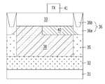
도 1은 종래기술에 따른 이미지 센서를 도시한 도면이다.1 is a view showing an image sensor according to the prior art.
도 1을 참조하여 종래기술에 따른 이미지 센서를 살펴보면, 기판(11)에 펀치쓰루방지층(12)이 형성된다. 펀치쓰루방지층(12)에 에피택셜 성장된 실리콘에피층(13)이 형성되고, 실리콘에피층(13)의 표면에 형성된 채널스탑영역(15a)에 포함되는 소자분리막(15b)이 형성된다. 그리고 실리콘에피층(13)상에 트랜스퍼트랜지스터의 게이트전극(Tx,16)이 형성된다. 게이트전극(16)의 일측 에지에 정렬되면서 실리콘에피층(13) 내부에 깊은 N형 확산층(17)이 형성되고, 깊은 N형 확산층(17)상부와 실리콘에피층(13) 표면 하부에 게이트전극(15) 일측에 정렬되는 얕은 P형 확산층(18)이 형성된다.Looking at the image sensor according to the prior art with reference to Figure 1, the punch-
결국, 깊은 N형 확산층(17)과 얕은 P형 확산층(18)으로 이루어진 포토다이오드(PD)가 형성된다.As a result, a photodiode PD consisting of a deep N-
이때, 크로스토크 및 광감도를 개선하기 위해, 깊은 N형 확산층(17)하부에 게이트전극(16)과 일부와 오버랩되는 포토다이오드확장영역(19)이 형성된다.In this case, in order to improve crosstalk and light sensitivity, a
그리고 인접픽셀간의 크로스토크를 방지하기 위해, 채널스탑영역(15a) 하부인 실리콘에피층(13)에 펀치쓰루방지층(12)과 접하는 P형 필드스탑영역(14)이 형성된다. 이때 P형 필드스탑영역(14)의 일측은 게이트전극(16) 중앙에 정렬되며, 포토다이오드확장영역(19) 일측과 접하도록 형성된다.In order to prevent crosstalk between adjacent pixels, a P-type
그리고 게이트전극(16)의 타측에 정렬되면서 P형 필드스탑영역(14) 내에 플로팅디퓨전영역(FD, 20)이 형성된다.The floating diffusion regions FD and 20 are formed in the P-type
하지만, 이미지 센서의 크로스토크 및 광감도를 향상시키기 위해서 형성된 포토다이오드확장영역(19)은 실질적으로 고농도의 N형 불순물 이온주입하여 형성하는데 어려움이 있다. 그 이유는 게이트전극(16)에 인가되는 제한된 전압 조건에서 특정 도즈 이상의 광전하가 정상적으로 게이트전극(16)의 채널을 통해 플로팅디퓨전영역(20)으로 전달되지 못하여 이미지래그 현상이 발생하기 때문이다. 즉, 공핍영역이 확장될 공간이 부족하여 이미지래그 및 감지특성이 열화되는 문제점이 있다.However, the
본 발명의 실시예는 포토다이오드영역을 확장함으로써, 이미지래그 및 크로스토크를 억제하고 광감도를 향상시킬 수 있는 이미지 센서 및 그 제조 방법을 제공한다.An embodiment of the present invention provides an image sensor and a method of manufacturing the same, which can suppress image lag and crosstalk and improve light sensitivity by expanding a photodiode region.
본 발명의 실시예에 따른 씨모스 이미지 센서는 기판; 상기 기판 표면에 형성된 펀치쓰루방지층; 상기 펀치쓰루방지층 상에 형성된 에피층; 상기 에피층 상에 형성된 트랜스퍼트랜지스터의 게이트전극; 상기 게이트전극의 일측에 정렬되어 상기 에피층에 형성된 포토다이오드; 상기 게이트전극의 타측에 정렬되어 상기 에피층에 형성된 플로팅디퓨전영역; 및 상기 포토다이오드 하부에 형성되며 상기 펀치쓰루방지층 표면과 접하도록 형성된 포토다이오드확장영역을 포함하며,CMOS image sensor according to an embodiment of the present invention is a substrate; A punchthrough prevention layer formed on the substrate surface; An epitaxial layer formed on the punchthrough prevention layer; A gate electrode of a transfer transistor formed on the epitaxial layer; A photodiode arranged on one side of the gate electrode and formed in the epi layer; A floating diffusion region arranged on the other side of the gate electrode and formed in the epi layer; And a photodiode extension region formed under the photodiode and in contact with a surface of the punchthrough prevention layer.
또한 기판을 형성하는 단계; 상기 기판 표면에 펀치쓰루방지층을 형성하는 단계; 상기 펀치쓰루방지층 상에 에피층을 형성하는 단계; 상기 에피층 내부에 상기 펀치쓰루방지층 표면까지 포토다이오드확장영역을 확작하여 형성하는 단계; 상기 포토다이오드확장영역 표면에 제1도전형의 제1도핑영역을 형성하는 단계; 상기 포토다이오드확장영역 상에 제1도핑영역의 일측과 오버랩되도록 형성된 포토다이오드; 상기 에피층 상에 상기 제1도핑영역과 오버랩하고, 상기 포토다이오드의 일측에 정렬되도록 게이트전극을 형성하는 단계; 및 상기 게이트전극 일측에 정렬되어 상기 에피층 내에 플로팅디퓨전영역을 형성하는 단계를 포함할 수 있다.Also forming a substrate; Forming a punch-through prevention layer on the substrate surface; Forming an epitaxial layer on the punchthrough prevention layer; Forming a photodiode extension region inside the epitaxial layer to a surface of the punchthrough prevention layer; Forming a first doped region of a first conductivity type on a surface of the photodiode extended region; A photodiode formed on the photodiode extension region to overlap one side of the first doped region; Forming a gate electrode on the epi layer, the gate electrode overlapping the first doped region and aligned with one side of the photodiode; And forming a floating diffusion region in the epi layer aligned with one side of the gate electrode.
본 기술은 종래 포토다이오드확장영역을 플로팅디퓨전영역 하부까지 확장하고 펀치쓰루방지층과 접하도록 형성함으로써 포토다이오드의 캐패시티 면적을 용이하게 확보하여 광감도를 향상시킬 수 있다. 그리고 플로팅디퓨전영역 하부와 포토다이오드확장영역 사이에 제1도전형의 제1도핑영역을 형성함으로써 광전하 전달 효율을 상승시켜 이미지래그를 개선시킬 수 있는 효과가 있다.The present technology extends the photodiode extension region to the lower portion of the floating diffusion region and contacts the punch-through prevention layer, thereby easily securing the capacitive area of the photodiode, thereby improving light sensitivity. In addition, the first doping region of the first conductivity type is formed between the lower portion of the floating diffusion region and the photodiode expansion region to increase the photocharge transfer efficiency, thereby improving the image lag.
또한 포토다이오드확장영역의 양 측벽이 제1도전형의 웰영역으로 감싸여져 다른 인접 픽셀로 전하가 유입되는 크로스토크 현상을 막아주는 효과가 있다.In addition, both sidewalls of the photodiode extension region may be surrounded by the well region of the first conductivity type, thereby preventing crosstalk phenomenon in which charge is introduced into another adjacent pixel.
도 1은 종래기술에 따른 씨모스 이미지센서를 도시한 도면.
도 2는 본 발명의 일실시예에 따른 이미지 센서를 도시한 단면도.
도 3a 내지 도 3h는 본 발명의 일실시예에 따른 이미지 센서의 제조 방법을 도시한 단면도.
도 4a 내지 도 4h는 본 발명의 일실시예에 따른 이미지 센서의 제조 방법을 도시한 평면도.1 shows a CMOS image sensor according to the prior art.
2 is a cross-sectional view showing an image sensor according to an embodiment of the present invention.
3A to 3H are cross-sectional views illustrating a method of manufacturing an image sensor according to an embodiment of the present invention.
4A to 4H are plan views illustrating a method of manufacturing an image sensor according to an embodiment of the present invention.
이하 본 발명이 속하는 기술분야에서 통상의 지식을 가진자가 본 발명의 기술적 사상을 용이하게 실시할 수 있을 정도로 상세히 설명하기 위하여, 본 발명의 가장 바람직한 실시예를 첨부도면을 참조하여 설명하기로 한다.Hereinafter, the most preferred embodiments of the present invention will be described in detail with reference to the accompanying drawings so that those skilled in the art may easily implement the technical idea of the present invention.
도 2는 본 발명의 일실시예에 따른 씨모스 이미지센서를 도시한 단면도이다.2 is a cross-sectional view illustrating a CMOS image sensor according to an exemplary embodiment of the present invention.
도 2를 참조하면, 기판(21) 표면에 고농도 P형 불순물을 도핑시켜 형성된 펀치쓰루방지층(22)이 형성된다. 펀치쓰루방지층(22)이 형성된 기판상에 에피택셜 성장된 실리콘에피층(23)이 형성되고, 실리콘층(23)의 표면으로부터 펀치쓰루방지층(22)의 상부와 이격되어 형성된 채널스탑영역(24a) 내에 소자분리막(24b)이 형성된다.Referring to FIG. 2, a punch-
여기서 채널스탑영역(24a)은 소자를 분리시켜주는 역할을 한다.Here, the
그리고 실리콘에피층(23) 상에 트랜스퍼트랜지스터의 게이트전극(Tx, 30)가 형성된다.The gate electrodes Tx and 30 of the transfer transistor are formed on the silicon
계속해서, 게이트전극(30) 일측 에지에 정렬되면서 실리콘에피층(23) 내에 소자분리막(24)의 일측에 정렬되는 깊은 N형 확산층(28) 형성되고, 깊은 N형 확산층(28) 상부와 실리콘에피층(23) 표면 하부에 게이트전극(36)의 일측에 정렬되는 얕은 P형 확산층(29)이 형성된다.Subsequently, a deep N-
결국, 깊은 N형 확산층(28)과 얕은 P형 확산층(29)으로 이루어진 포토다이오드가(PD)가 형성된다.As a result, a photodiode PD consisting of a deep N-
그리고, 포토다이오드(PD)를 정렬시키는 게이트전극(30)의 일측과 반대로 게이트전극(30)의 타측에 정렬되어 N형 불순물이 도핑된 플로팅디퓨젼영역(31)이 형성된다.In addition, a
여기서, 본 발명의 새로운 구조는 실리콘에피층(23) 내 깊은 N형 확산층(28) 하부에 게이트전극(30) 및 플로팅디퓨전영역(31)과 오버랩되어 포토다이오드확장영역(26)이 형성된다. 포토다이오드확장영역(26)은 포토다이오드 캐패시티를 최대한 확보하기 위해 배치된 구조이다.The new structure of the present invention overlaps the
그리고 크로스토크 현상을 막기위해, 채널스탑영역(24a) 하부에 펀치쓰루방지층(20)과 접하며 포토다이오드확장영역(24)의 측벽을 감싸는 P 형 불순물이 도핑된 웰영역(25)이 형성된다.In order to prevent the crosstalk phenomenon, a
이때 웰영역(25)은 적정 에너지 및 도즈 조건, 예컨대 P형 불순물의 물질인 붕소(B, Boron)을 이온주입하고, 1×10¹²~2×10¹²dose/cm2 수준으로 2~3번에 걸쳐 에너지 단계를 나누어 형성될 수 있다.In this case, the
그리고 포토다이오드확장영역(26) 상부와 플로팅디퓨전영역(31) 하부 및 게이트전극(30) 하부 사이에 P형 불순물이 도핑된 제1도핑영역(27)이 형성된다.A first
제1도핑영역(27)은 실리콘에피층(23) 표면으로부터 0.5μm~0.8μm 깊이에 형성되며, 얕은 P형 확산층(29), 채널스탑영역(24a), 웰영역(25) 및 펀치쓰루방지층(23) 사이에 전기적인 연결(electrical connection)을 최대화함과 동시에 포토다이오드확장영역(26)에서 플로팅디퓨전영역(31)으로 광전하의 전달 영역을 발달시켜줌으로써 이미지래그 특성 열화를 개선시킨다.The first
도 3a 내지 도 3h 및 도 4a 내지 도 4h는 본 발명의 일실시예에 따른 씨모스 이미지 센서 제조 방법을 도시한 공정 단면도 및 평면도이며, 도 3a 내지 도 3h는 도 4a 내지 도 4h에 도시된 A-A'절취선을 따라 도시한 단면도이다.3A to 3H and 4A to 4H are cross-sectional views and plan views illustrating a method of manufacturing a CMOS image sensor according to an exemplary embodiment of the present invention, and FIGS. 3A to 3H are shown in FIGS. 4A to 4H. -A 'is a sectional view along the cut line.
도 3a 및 도 4a를 참조하면, 기판(31)상에 펀치쓰루방지층(32)을 형성한다. 펀치쓰루방지층(32)은 기판에 고농도 P형 불순물을 도핑시켜 형성된 불순물층일 수 있다.3A and 4A, a punch-
펀치쓰루방지층(32)을 형성하기 위한 불순물로는 P형 불순물 예컨대, 붕소(B, Boron)를 사용할 수 있다. 펀치쓰루방지층(52)의 특성을 위해 불순물의 도핑농도는 적어도 1×10¹⁸ atoms/cm2이상이 되도록 형성할 수 있다.P-type impurities such as boron (B) may be used as impurities for forming the punch-through
펀치쓰루방지층(32)이 형성된 기판상에 실리콘에피층(33)을 형성한다. 실리콘에피층(33)은 포토다이오드와 같은 씨모스 이미지센서의 구성요소가 형성될 층으로, 단결정상태를 갖도록 형성한다. 단결정상태를 갖는 실리콘에피층(33)은 에피택셜 성장법을 사용하여 형성할 수 있다.The silicon
실리콘에피층(33)은 불순물이 도핑된 도프드 실리콘에피층으로 형성할 수 있다. 불순물은 펀치쓰루방지층(32)과 동일한 도전형(P형)일 수 있으며, 도핑농도는 펀치쓰루방지층(32)보다 낮은 도핑농도를 갖는다.The
도 3b 및 도 4b를 참조하면, 실리콘에피층(33)에 P형 불순물을 이온주입하여 펀치쓰루방지층(32)과 접하는 웰영역(35)을 형성한다.3B and 4B, a
웰영역(35)을 형성하는 방법은 실리콘에피층(33) 상에 감광막을 도포한 후, 감광막을 선택적으로 패터닝하여 P형 불순물을 이온주입하기 위한 제1마스크패턴(34)을 형성한다.In the method of forming the
이때, 제1마스크패턴(34)의 양측은 실리콘에피층의 양측에 정렬되어 웰영역(35)이 형성될 실리콘에피층(33) 표면을 노출시킨다.At this time, both sides of the
웰영역(35)은 실리콘에피층(33) 전면에 저농도의 P형 불순물인 붕소(B, Boron)를 1×10¹² ~ 2×10¹²dose/cm2정도 수준으로 2~3회에 걸쳐 에너지 단계를 나누어 이온주입하여 형성한다.In the
여기서, 웰영역(35)을 형성하는 이유는 후속 포토다이오드확장영역을 최대한 확보함과 동시에 인접 픽셀간의 크로스토크 현상을 동시에 확보함으로써, 포토다이오드(PD)의 포화도(Qsat) 확보와 동시에 우수한 광감도특성을 얻을 수 있으며, 포토다이오드(PD)에 입사된 빛에 의해 생성된 전자가 재결합하거나, 전자가 포토다이오드의 공핍영역으로 모이지 않고 인접 픽셀로 전달되어 왜곡을 발생시키는 크로스토크 현상을 개선시켜 주기 때문이다.Here, the reason for forming the
도 3c 및 도 4c를 참조하면, 실리콘에피층(33)에 이웃한 단위픽셀을 분리시키는 소자분리막(36b)을 갖는 채널스탑영역(36a)을 형성한다.Referring to FIGS. 3C and 4C, the
도면에 도시되지 않았지만, 실리콘에피층(33)내에 채널스탑영역(36a)을 형성하기 위한 채널스탑마스크를 실리콘에피층(33) 상에 형성한다. 그리고 채널스탑마스크를 이온주입마스크로 이용하여 실리콘에피층(33) 내에 P형 불순물을 이온주입하여 채널스탑영역(36a)을 형성한다.Although not shown in the figure, a channel stop mask for forming the
계속해서 소자분리막(36b)을 형성하기 위해 실리콘에피층(33) 상에 소자분리마스크를 형성한다. 이때 소자분리마스크를 형성하기 위한 마스크 공정은 STI(Shallow Trench Isolation)공정을 적용한다.Subsequently, an element isolation mask is formed on the
예컨데, 실리콘에피층(33) 상에 패드산화막(pad oxide)과 패드질화막(pad nitride)을 차례로 증착한 후, 패드질화막 상에 감광막을 도포한 후 노광 및 현상으로 패터닝하여 트렌치를 형성하기 위한 소자분리마스크를 형성한다.For example, a device for forming a trench by sequentially depositing a pad oxide film and a pad nitride film on the
그리고, 소자분리마스크에 의해 노출된 패드산화막과 패드질화막을 동시에 식각하여 실리콘에피층(33)의 표면 일부를 노출시키고, 계속해서 노출된 실리콘에피층(33)을 웰영역(35) 방향으로 일정 깊이까지 식각하여 트렌치를 형성한다.The pad oxide film and the pad nitride film exposed by the device isolation mask are simultaneously etched to expose a part of the surface of the
그 다음에 소자분리마스크를 제거한 후 트렌치를 포함한 전면에 갭필(gapfill) 특성이 우수한 화학기상증착방식(Chemical Vapor Deposition:CVD)의 산화막을 증착하고, 패드질화막 및 패드 산화막이 제거될 때까지 산화막을 화학적기계적연마(Chemical Mechanical Polishing:CMP)하여 평탄화하여 평탄화된 산화막을 습식식각으로 등방성식각하여 트렌치에 매립되는 소자분리막(36b)을 형성한다.Then, after removing the device isolation mask, an oxide film of chemical vapor deposition (CVD) having excellent gapfill characteristics is deposited on the entire surface including the trench, and the oxide film is removed until the pad nitride film and the pad oxide film are removed. The chemical mechanical polishing (CMP) is performed to planarize and isotropically etch the planarized oxide film by wet etching to form an
계속해서, 포토다이오드(PD)의 캐패시티를 확장하기 위해서 웰영역(35) 내에 펀치쓰루방지층(32)과 접하는 포토다이오드확장영역(38)을 형성한다. 포토다이오드확장영역(38)은 포토다이오드 캐패시티를 최대한 확보하기 위해 배치된 구조이다.Subsequently, in order to expand the capacity of the photodiode PD, a
포토다이오드확장영역(38)을 형성하는 방법은 실리콘에피층(33) 상에 감광막을 도포한 후, 감광막을 선택적으로 패터닝하여 N형 불순물을 이온주입하기 위한 제2마스크패턴(37)을 형성한다. 그리고 형성된 제2마스크패턴(37)에 의해 노출된 실리콘에피층(33), 자세히는 웰영역(35)에 N형 불순물을 이온주입하여 웰영역(35) 내에 포토다이오드확장영역(38)을 형성한다.In the method for forming the
포토다이오드확장영역(38)은 웰영역(35) 내부에 적정 에너지 및 도즈 조건, 예컨데 N형 불순물인 인(Ph) 또는 유사 N형 불순물을 웰영역(35)에 웰영역(35)의 P형 불순물의 도즈 조건을 고려하여 이온주입하고, 2×10¹²~4×10¹²dose/cm2 수준으로 두세번에 걸쳐 에너지 단계를 나누어 진행함에 따라 형성된다.The
도 3d 및 도 4d를 참조하면, 제3마스크패턴(39)을 이온주입마스크로하여 포토다이오드확장영역(38) 일부 영역에 P형 불순물을 이온주입하여 제1도핑영역(40)을 형성한다.3D and 4D, the first
제1도핑영역(40)은 후속 게이트전극 및 후속 플로팅디퓨전영역과 오버랩되며 후속 포토다이오드(PD) 일부 영역까지 확장되어 형성된다. 자세히는, 제1도핑영역(40)은 실리콘에피층(33) 표면으로부터 0.5μm~0.8μm 범위의 깊이에 이르는 포토다이오드확장영역(38) 일부 영역에 후속 게이트전극 및 후속 플로팅디퓨전영역과 오버랩되도록 P형 불순물을 이온주입하여 형성한다. 그리고 후속 얕은 P형 확산층, 채널스탑영역(36a), 웰영역(35) 및 펀치쓰루방지층(32) 사이에 전기적인 연결(electrical connection)을 최대화함과 동시에 포토다이오드확장영역(38)에서 후속 플로팅디퓨전영역으로 광전하의 전달 영역을 발달시켜줌으로써 이미지래그 특성 열화를 개선시킨다.The first
도 3e 및 도 4e를 참조하면, 실리콘에피층(33)상에 게이트전극(41)을 형성한다.3E and 4E, the
즉, 게이트전극(41)은 제1도핑영역(40)의 일측과 오버랩되어 실리콘에피층(33)상에 형성된다.That is, the
도 3f 및 도 4f를 참조하면, 게이트전극(41)을 포함한 전면에 감광막을 도포한 후, 감광막을 선택적으로 패터닝하여 고에너지로 저농도 N형 불순물을 이온주입하기 위한 제4마스크패턴(42)을 형성한다.Referring to FIGS. 3F and 4F, after applying a photoresist film to the entire surface including the
이때, 제4마스크패턴(42)의 일측은 게이트전극(41) 상의 일측에 정렬되고 타측은 채널스탑영역(36a) 상의 일측에 정렬되어 포토다이오드가 형성될 실리콘에피층(33) 표면을 노출시킨다.At this time, one side of the
다음으로, 제4마스크패턴(42)을 이온주입마스크로 하여, N형 불순물을 이온주입하여 실리콘에피층(33) 내에 포토다이오드확장영역(38)의 표면까지 깊은 N형 확산층(43)을 형성한다.Next, using the
이때, 깊은 N형 확산층(43)의 일측은 게이트전극(41)의 일측에 정렬되고, 타측은 절연접합영역(36a)의 일측면과 접한다.At this time, one side of the deep N-
계속해서, 제4마스크패턴(42)을 재사용하여 제4마스크패턴(42)에 의해 노출된 실리콘에피층(33), 자세히는 깊은 N형 확산층(43) 상부와 실리콘에피층(33) 표면 하부에 게이트전극(41)의 일측에 정렬되도록 얕은 P형 확산층(44)을 형성한다.Subsequently, the
상술한 P형 불순물의 이온주입을 통해 얕은 P형 확산층(44)과 깊은 N형 확산층(43)으로 이루어지는 PN접합이 형성되고, 포토다이오드확장영역(38)/깊은 N형 확산층(43)/ 얕은 P형 확산층(44)으로 이루어지는 확장된 포토다이오드(PD)가 형성된다.The ion implantation of the P-type impurity described above forms a PN junction composed of a shallow P-
도 3g 및 도 4g를 참조하면, 제4마스크패턴(42)을 제거한 후, 전면에 감광막을 도포하고 노광 및 현상으로 패터닝하여 게이트전극(41)의 타측에 노출된 실리콘에피층(33)을 노출시키는 제5마스크패턴(45)을 형성한다.Referring to FIGS. 3G and 4G, after removing the
다음으로, 제5마스크패턴(45)을 이온주입 마스크로하여 N형 불순물을 이온주입하여 플로팅디퓨전영역(46)을 형성한다. 그리고 제5마스크패턴(45)을 제거하여 도 3h 및 도 4h와 같이 씨모스 이미지센서를 완성한다.Next, the floating
본 발명의 기술 사상은 상기 바람직한 실시예에 따라 구체적으로 기술되었으나, 상기 실시예는 그 설명을 위한 것이며, 그 제한을 위한 것이 아님을 주의하여야 한다. 또한, 본 발명의 기술분야의 통의 전문가라면 본 발명의 기술사상의 범위내의 다양한 실시예가 가능함을 이해할 수 있을 것이다.Although the technical spirit of the present invention has been described in detail according to the above preferred embodiment, it should be noted that the above embodiment is for the purpose of description and not of limitation. In addition, those skilled in the art will appreciate that various embodiments within the scope of the technical idea of the present invention are possible.
21,31:기판 22,32:펀치쓰루방지층
23,33:실리콘에피층 24a,36a:채널스탑영역
24b,36b:소자분리막 25,35:웰영역
26,38:포토다이오드영역 27,40:제1영역
28,43:깊은 N 확산층 29,44:얕은 P 확산층
30,41:게이트전극 31,46:플로팅디퓨전영역
34:제1마스크패턴 37:제2마스크패턴
39:제3마스크패턴 42:제4마스크패턴
45:제5마스크패턴21, 31:
23, 33:
24b and 36b: device isolation layers 25 and 35: well region
26, 38:
28,43: deep
30,41
34: first mask pattern 37: second mask pattern
39: third mask pattern 42: fourth mask pattern
45: fifth mask pattern
Claims (20)
Translated fromKorean상기 기판 표면에 형성된 펀치쓰루방지층;
상기 펀치쓰루방지층 상에 형성된 에피층;
상기 에피층 상에 형성된 트랜스퍼트랜지스터의 게이트전극;
상기 게이트전극의 일측에 정렬되어 상기 에피층에 형성된 포토다이오드;
상기 게이트전극의 타측에 정렬되어 상기 에피층에 형성된 플로팅디퓨전영역; 및
상기 포토다이오드 하부에 형성되며 상기 펀치쓰루방지층의 표면과 접하도록 형성된 포토다이오드확장영역을 포함하고,
상기 포토다이오드확장영역의 일측은 상기 포토다이오드와 수직 방향으로 오버랩되고, 상기 포토다이오드확장영역의 타측은 상기 플로팅디퓨전영역의 하부까지 확장되어 상기 플로팅디퓨전영역과 상기 수직 방향으로 오버랩되는 씨모스 이미지센서.
Board;
A punchthrough prevention layer formed on the substrate surface;
An epitaxial layer formed on the punchthrough prevention layer;
A gate electrode of a transfer transistor formed on the epitaxial layer;
A photodiode arranged on one side of the gate electrode and formed in the epi layer;
A floating diffusion region arranged on the other side of the gate electrode and formed in the epi layer; And
A photodiode extension region formed under the photodiode and formed to be in contact with the surface of the punch-through prevention layer;
One side of the photodiode expansion region overlaps the photodiode in a vertical direction, and the other side of the photodiode expansion region extends to a lower portion of the floating diffusion region and overlaps the floating diffusion region in the vertical direction. .
상기 포토다이오드확장영역의 양 측면을 감싸는 제1도전형의 웰영역을 더 포함하는 씨모스 이미지센서.
The method of claim 1,
And a well region of a first conductivity type surrounding both sides of the photodiode extension region.
상기 포토다이오드는
상기 게이트전극의 일측에 정렬되어 상기 에피층 내부에 형성된 N형 확산층; 및
상기 N형 확산층 상에 형성된 P형 확산층을 포함하고,
상기 포토다이오드확장영역은 상기 N형 확산층과 접하는 씨모스 이미지 센서.
The method of claim 1,
The photodiode
An N-type diffusion layer aligned with one side of the gate electrode and formed in the epi layer; And
P-type diffusion layer formed on the N-type diffusion layer,
And the photodiode extension region is in contact with the N-type diffusion layer.
상기 포토다이오드확장영역은 N형 불순물이 도핑된 씨모스 이미지 센서.
The method of claim 3,
The photodiode expansion region is a CMOS image sensor doped with N-type impurities.
상기 게이트전극 및 상기 플로팅디퓨전영역의 하부에 형성된 제1도핑영역을 더 포함하는 씨모스 이미지센서.
The method of claim 1,
And a first doped region formed below the gate electrode and the floating diffusion region.
상기 플로팅디퓨전영역은 상기 웰영역보다 낮은 불순불 도핑농도를 갖는 씨모스 이미지센서
The method of claim 2,
The floating diffusion region has a CMOS image sensor having a lower impurity doping concentration than the well region.
상기 제1도핑영역의 일측은 상기 포토다이오드의 일부와 오버랩되고, 상기 제1도핑영역의 타측은 상기 플로팅디퓨전영역과 오버랩된 씨모스 이미지 센서.
The method of claim 5,
One side of the first doped region overlaps a portion of the photodiode, and the other side of the first doped region overlaps with the floating diffusion region CMOS image sensor.
상기 기판상에 펀치쓰루방지층을 형성하는 단계;
상기 펀치쓰루방지층 상에 에피층을 형성하는 단계;
상기 에피층 내부에 상기 펀치쓰루방지층과 접촉되는 포토다이오드확장영역을 형성하는 단계;
상기 포토다이오드확장영역 표면의 일부에 제1도핑영역을 형성하는 단계;
상기 에피층 상에 상기 제1도핑영역과 오버랩된 게이트전극을 형성하는 단계;
포토다이오드확장영역 상에 상기 게이트 전극의 일측과 정렬된 포토다이오드를 형성하는 단계; 및
상기 제1 도핑영역 상에 상기 게이트전극 타측에 정렬된 플로팅디퓨전영역을 형성하는 단계
를 포함하며, 상기 포토다이오드확장영역의 일측은 상기 포토다이오드와 수직 방향으로 오버랩되며, 상기 포토다이오드확장영역의 타측은 상기 플로팅디퓨젼영역의 하부까지 확장되어 상기 플로팅디퓨젼영역과 상기 수직 방향으로 오버랩되는 씨모스 이미지센서 제조 방법.
Forming a substrate;
Forming a punch-through prevention layer on the substrate;
Forming an epitaxial layer on the punchthrough prevention layer;
Forming a photodiode expansion region in contact with the punch-through prevention layer in the epi layer;
Forming a first doped region on a portion of a surface of the photodiode extended region;
Forming a gate electrode overlapping the first doped region on the epitaxial layer;
Forming a photodiode aligned with one side of the gate electrode on the photodiode extension region; And
Forming a floating diffusion region arranged on the other side of the gate electrode on the first doped region
One side of the photodiode expansion region overlaps the photodiode in a vertical direction, and the other side of the photodiode expansion region extends to a lower portion of the floating diffusion region in the vertical direction and the floating diffusion region. Overlapping CMOS image sensor manufacturing method.
상기 포토다이오드확장영역을 형성하는 단계 이전에, 상기 에피층 내에 상기 펀치쓰루방지층과 접촉하는 제1 도전형의 웰영역 형성하는 단계; 및
상기 에피층 내에 채널스탑영역 및 소지분리층의 적층을 포함하는 소자분리구조물을 형성하는 단계
를 더 포함하는 씨모스 이미지센서 제조 방법.
The method of claim 8,
Prior to forming the photodiode extension region, forming a well region of a first conductivity type in contact with the punch-through prevention layer in the epitaxial layer; And
Forming an isolation structure including a stack of channel stop regions and a base isolation layer in the epitaxial layer
CMOS image sensor manufacturing method comprising a more.
상기 웰영역은 상기 포토다이오드확장영역의 양측을 둘러싸는 형태로 형성되는 씨모스 이미지센서 제조 방법.
The method of claim 9,
And the well region is formed to surround both sides of the photodiode extension region.
상기 포토다이오드확장영역은 상기 웰영역보다 낮은 불순물 도핑농도를 갖는 씨모스 이미지센서 제조 방법.
The method of claim 9,
And the photodiode extension region has a lower impurity doping concentration than the well region.
상기 채널스탑영역은 P형 불순물을 이온주입하여 형성되는 씨모스 이미지센서 제조 방법.
The method of claim 9,
And the channel stop region is formed by ion implantation of P-type impurities.
상기 포토다이오드를 형성하는 단계는
상기 게이트전극의 일측에 정렬되어 형성된 상기 에피층 내에 N형 확산층을 형성하는 단계; 및
상기 N형 확산층 상부에 P형 확산층을 현성하는 단계를 포함하고,
상기 포토다이오드확장영역은 상기 N형 확산층과 접하는 씨모스 이미지 센서 제조 방법.
The method of claim 9,
Forming the photodiode
Forming an N-type diffusion layer in the epitaxial layer formed on one side of the gate electrode; And
Forming a P-type diffusion layer on the N-type diffusion layer,
And the photodiode extension region is in contact with the N-type diffusion layer.
상기 포토다이오드확장영역은 N형 불순물을 이온주입하여 형성되는 씨모스 이미지센서 제조 방법.
The method of claim 13,
And the photodiode expansion region is formed by ion implantation of N-type impurities.
상기 제1도핑영역, 상기 P형 확산층, 상기 채널스탑영역, 상기 웰영역 및 상기 펀치쓰루방지층은 서로 연결되도록 형성되는 씨모스 이미지센서 제조 방법.
The method of claim 14,
And the first doped region, the P-type diffusion layer, the channel stop region, the well region, and the punchthrough prevention layer are connected to each other.
상기 제1도핑영역의 일측은 상기 포토다이오드의 일부와 오버랩되고, 상기 제1도핑영역의 타측은 상기 플로팅디퓨젼영역과 오버랩되는 씨모스 이미지센서 제조 방법.The method of claim 8,
Wherein one side of the first doped region overlaps a portion of the photodiode, and the other side of the first doped region overlaps the floating diffusion region.
Priority Applications (2)
| Application Number | Priority Date | Filing Date | Title |
|---|---|---|---|
| KR1020120073978AKR102009931B1 (en) | 2012-07-06 | 2012-07-06 | Cmos image sensor and method for fabricating the same |
| US13/599,999US8748955B2 (en) | 2012-07-06 | 2012-08-30 | CMOS image sensor and method for fabricating the same |
Applications Claiming Priority (1)
| Application Number | Priority Date | Filing Date | Title |
|---|---|---|---|
| KR1020120073978AKR102009931B1 (en) | 2012-07-06 | 2012-07-06 | Cmos image sensor and method for fabricating the same |
Publications (2)
| Publication Number | Publication Date |
|---|---|
| KR20140006595A KR20140006595A (en) | 2014-01-16 |
| KR102009931B1true KR102009931B1 (en) | 2019-08-13 |
Family
ID=49877867
Family Applications (1)
| Application Number | Title | Priority Date | Filing Date |
|---|---|---|---|
| KR1020120073978AExpired - Fee RelatedKR102009931B1 (en) | 2012-07-06 | 2012-07-06 | Cmos image sensor and method for fabricating the same |
Country Status (2)
| Country | Link |
|---|---|
| US (1) | US8748955B2 (en) |
| KR (1) | KR102009931B1 (en) |
Families Citing this family (3)
| Publication number | Priority date | Publication date | Assignee | Title |
|---|---|---|---|---|
| JP2014199898A (en)* | 2013-03-11 | 2014-10-23 | ソニー株式会社 | Solid-state imaging element and method of manufacturing the same, and electronic equipment |
| US10163963B2 (en)* | 2017-04-05 | 2018-12-25 | Semiconductor Components Industries, Llc | Image sensors with vertically stacked photodiodes and vertical transfer gates |
| CN119486297B (en)* | 2025-01-13 | 2025-04-22 | 合肥晶合集成电路股份有限公司 | Image sensor and preparation method thereof |
Citations (2)
| Publication number | Priority date | Publication date | Assignee | Title |
|---|---|---|---|---|
| JP2002353431A (en)* | 2001-05-22 | 2002-12-06 | Canon Inc | Photoelectric conversion device and method of manufacturing the same |
| KR100761048B1 (en)* | 2006-08-24 | 2007-09-21 | 주식회사 쎄이미지 | High sensitivity CD image sensor and its manufacturing method |
Family Cites Families (6)
| Publication number | Priority date | Publication date | Assignee | Title |
|---|---|---|---|---|
| KR20050040026A (en) | 2003-10-27 | 2005-05-03 | 매그나칩 반도체 유한회사 | Photo diode of cmos image sensor |
| US7419844B2 (en)* | 2006-03-17 | 2008-09-02 | Sharp Laboratories Of America, Inc. | Real-time CMOS imager having stacked photodiodes fabricated on SOI wafer |
| KR101019279B1 (en)* | 2007-07-24 | 2011-03-07 | 크로스텍 캐피탈, 엘엘씨 | Image sensor and its manufacturing method |
| KR100997326B1 (en)* | 2007-12-27 | 2010-11-29 | 주식회사 동부하이텍 | Image sensor and its manufacturing method |
| KR100962470B1 (en) | 2008-05-09 | 2010-06-14 | 한국과학기술원 | Pixel Circuit of Solid State Imaging Device |
| KR20100040017A (en) | 2008-10-09 | 2010-04-19 | 주식회사 동부하이텍 | Image sensor and method for manufacturing thereof |
- 2012
- 2012-07-06KRKR1020120073978Apatent/KR102009931B1/ennot_activeExpired - Fee Related
- 2012-08-30USUS13/599,999patent/US8748955B2/enactiveActive
Patent Citations (2)
| Publication number | Priority date | Publication date | Assignee | Title |
|---|---|---|---|---|
| JP2002353431A (en)* | 2001-05-22 | 2002-12-06 | Canon Inc | Photoelectric conversion device and method of manufacturing the same |
| KR100761048B1 (en)* | 2006-08-24 | 2007-09-21 | 주식회사 쎄이미지 | High sensitivity CD image sensor and its manufacturing method |
Also Published As
| Publication number | Publication date |
|---|---|
| US20140008709A1 (en) | 2014-01-09 |
| US8748955B2 (en) | 2014-06-10 |
| KR20140006595A (en) | 2014-01-16 |
Similar Documents
| Publication | Publication Date | Title |
|---|---|---|
| US11901388B2 (en) | Device over photodetector pixel sensor | |
| KR100619396B1 (en) | CMOS Image sensor and its fabricating method | |
| US11502117B2 (en) | Image sensor including conductive connection pattern | |
| JP5150050B2 (en) | CMOS image sensor and manufacturing method thereof | |
| KR102175615B1 (en) | Cmos image sensor with shallow trench edge doping | |
| KR101485653B1 (en) | Cmos image sensors and method for forming the same | |
| TW201133813A (en) | CMOS image sensor with self-aligned photodiode implants | |
| US8124438B2 (en) | Method of fabricating CMOS image sensor | |
| KR101436215B1 (en) | Gate Electrodes with Notches and Methods for Forming the Same | |
| JP4061609B2 (en) | Image sensor having stretched pinned photodiode and method for manufacturing the same | |
| KR101517664B1 (en) | Self-aligned implantation process for forming junction isolation regions | |
| KR102009931B1 (en) | Cmos image sensor and method for fabricating the same | |
| KR102013789B1 (en) | Cmos image sensor and method for fabricating the same | |
| KR101038789B1 (en) | Image sensor and manufacturing method | |
| JP2009071308A (en) | Manufacturing method of image sensor | |
| KR100893054B1 (en) | Image sensor and its manufacturing method that can prevent crosstalk | |
| CN104332481B (en) | Imaging sensor and forming method thereof | |
| KR100935269B1 (en) | Image sensor and its manufacturing method | |
| KR100870823B1 (en) | Image sensor and manufacturing method | |
| KR20040059759A (en) | CMOS image sensor with new shape isolation layer and method for fabricating the same | |
| KR100790286B1 (en) | Image sensor manufacturing method | |
| KR20040059429A (en) | Fabricating method for CMOS image sensor | |
| KR20030057709A (en) | Image sensor and method for fabricating the same | |
| KR20060095535A (en) | CMOS image sensor and its manufacturing method | |
| KR20100046503A (en) | Image sensor and method for manufacturing the sensor |
Legal Events
| Date | Code | Title | Description |
|---|---|---|---|
| PA0109 | Patent application | St.27 status event code:A-0-1-A10-A12-nap-PA0109 | |
| PN2301 | Change of applicant | St.27 status event code:A-3-3-R10-R13-asn-PN2301 St.27 status event code:A-3-3-R10-R11-asn-PN2301 | |
| PG1501 | Laying open of application | St.27 status event code:A-1-1-Q10-Q12-nap-PG1501 | |
| PN2301 | Change of applicant | St.27 status event code:A-3-3-R10-R13-asn-PN2301 St.27 status event code:A-3-3-R10-R11-asn-PN2301 | |
| A201 | Request for examination | ||
| E13-X000 | Pre-grant limitation requested | St.27 status event code:A-2-3-E10-E13-lim-X000 | |
| P11-X000 | Amendment of application requested | St.27 status event code:A-2-2-P10-P11-nap-X000 | |
| P13-X000 | Application amended | St.27 status event code:A-2-2-P10-P13-nap-X000 | |
| PA0201 | Request for examination | St.27 status event code:A-1-2-D10-D11-exm-PA0201 | |
| D13-X000 | Search requested | St.27 status event code:A-1-2-D10-D13-srh-X000 | |
| D14-X000 | Search report completed | St.27 status event code:A-1-2-D10-D14-srh-X000 | |
| E902 | Notification of reason for refusal | ||
| PE0902 | Notice of grounds for rejection | St.27 status event code:A-1-2-D10-D21-exm-PE0902 | |
| E13-X000 | Pre-grant limitation requested | St.27 status event code:A-2-3-E10-E13-lim-X000 | |
| P11-X000 | Amendment of application requested | St.27 status event code:A-2-2-P10-P11-nap-X000 | |
| P13-X000 | Application amended | St.27 status event code:A-2-2-P10-P13-nap-X000 | |
| E701 | Decision to grant or registration of patent right | ||
| PE0701 | Decision of registration | St.27 status event code:A-1-2-D10-D22-exm-PE0701 | |
| GRNT | Written decision to grant | ||
| PR0701 | Registration of establishment | St.27 status event code:A-2-4-F10-F11-exm-PR0701 | |
| PR1002 | Payment of registration fee | St.27 status event code:A-2-2-U10-U11-oth-PR1002 Fee payment year number:1 | |
| PG1601 | Publication of registration | St.27 status event code:A-4-4-Q10-Q13-nap-PG1601 | |
| PR1001 | Payment of annual fee | St.27 status event code:A-4-4-U10-U11-oth-PR1001 Fee payment year number:4 | |
| PC1903 | Unpaid annual fee | St.27 status event code:A-4-4-U10-U13-oth-PC1903 Not in force date:20230807 Payment event data comment text:Termination Category : DEFAULT_OF_REGISTRATION_FEE | |
| PC1903 | Unpaid annual fee | St.27 status event code:N-4-6-H10-H13-oth-PC1903 Ip right cessation event data comment text:Termination Category : DEFAULT_OF_REGISTRATION_FEE Not in force date:20230807 | |
| P22-X000 | Classification modified | St.27 status event code:A-4-4-P10-P22-nap-X000 |