KR102009017B1 - Oxide thin film transistor for display device and method for fabricating the same - Google Patents
Oxide thin film transistor for display device and method for fabricating the sameDownload PDFInfo
- Publication number
- KR102009017B1 KR102009017B1KR1020120109501AKR20120109501AKR102009017B1KR 102009017 B1KR102009017 B1KR 102009017B1KR 1020120109501 AKR1020120109501 AKR 1020120109501AKR 20120109501 AKR20120109501 AKR 20120109501AKR 102009017 B1KR102009017 B1KR 102009017B1
- Authority
- KR
- South Korea
- Prior art keywords
- alloy
- layer
- oxide
- gate insulating
- forming
- Prior art date
- Legal status (The legal status is an assumption and is not a legal conclusion. Google has not performed a legal analysis and makes no representation as to the accuracy of the status listed.)
- Active
Links
Images


Classifications
- H—ELECTRICITY
- H10—SEMICONDUCTOR DEVICES; ELECTRIC SOLID-STATE DEVICES NOT OTHERWISE PROVIDED FOR
- H10D—INORGANIC ELECTRIC SEMICONDUCTOR DEVICES
- H10D30/00—Field-effect transistors [FET]
- H10D30/60—Insulated-gate field-effect transistors [IGFET]
- H10D30/67—Thin-film transistors [TFT]
- H10D30/6757—Thin-film transistors [TFT] characterised by the structure of the channel, e.g. transverse or longitudinal shape or doping profile
- H—ELECTRICITY
- H01—ELECTRIC ELEMENTS
- H01L—SEMICONDUCTOR DEVICES NOT COVERED BY CLASS H10
- H01L21/00—Processes or apparatus adapted for the manufacture or treatment of semiconductor or solid state devices or of parts thereof
- H01L21/02—Manufacture or treatment of semiconductor devices or of parts thereof
- H01L21/02104—Forming layers
- H01L21/02107—Forming insulating materials on a substrate
- H01L21/02109—Forming insulating materials on a substrate characterised by the type of layer, e.g. type of material, porous/non-porous, pre-cursors, mixtures or laminates
- H01L21/02112—Forming insulating materials on a substrate characterised by the type of layer, e.g. type of material, porous/non-porous, pre-cursors, mixtures or laminates characterised by the material of the layer
- H01L21/02172—Forming insulating materials on a substrate characterised by the type of layer, e.g. type of material, porous/non-porous, pre-cursors, mixtures or laminates characterised by the material of the layer the material containing at least one metal element, e.g. metal oxides, metal nitrides, metal oxynitrides or metal carbides
- H01L21/02175—Forming insulating materials on a substrate characterised by the type of layer, e.g. type of material, porous/non-porous, pre-cursors, mixtures or laminates characterised by the material of the layer the material containing at least one metal element, e.g. metal oxides, metal nitrides, metal oxynitrides or metal carbides characterised by the metal
- H—ELECTRICITY
- H10—SEMICONDUCTOR DEVICES; ELECTRIC SOLID-STATE DEVICES NOT OTHERWISE PROVIDED FOR
- H10D—INORGANIC ELECTRIC SEMICONDUCTOR DEVICES
- H10D30/00—Field-effect transistors [FET]
- H10D30/01—Manufacture or treatment
- H10D30/021—Manufacture or treatment of FETs having insulated gates [IGFET]
- H10D30/031—Manufacture or treatment of FETs having insulated gates [IGFET] of thin-film transistors [TFT]
Landscapes
- Engineering & Computer Science (AREA)
- Physics & Mathematics (AREA)
- Condensed Matter Physics & Semiconductors (AREA)
- General Physics & Mathematics (AREA)
- Manufacturing & Machinery (AREA)
- Computer Hardware Design (AREA)
- Microelectronics & Electronic Packaging (AREA)
- Power Engineering (AREA)
- Thin Film Transistor (AREA)
Abstract
Translated fromKoreanDescription
Translated fromKorean본 발명은 박막 트랜지스터에 관한 것으로서, 보다 상세하게는 표시장치용 산화물 박막 트랜지스터 및 그 제조방법에 관한 것이다.The present invention relates to a thin film transistor, and more particularly, to an oxide thin film transistor for a display device and a method of manufacturing the same.
비약적으로 성장하고 있는 평판디스플레이 시장에서 가장 큰 응용 대상으로 TV(Television) 제품이 있다. 현재 TV용 패널로서 액정디스플레이(LCD; Liquid Crystal Display)가 주축을 이루고 있는 가운데, 유기발광디스플레이도 TV로의 응용을 위해 많은 연구가 진행되고 있다.The largest application in the rapidly growing flat panel display market is TV (Television) products. Currently, liquid crystal displays (LCDs) are mainly used as TV panels, and organic light emitting displays are also being researched for application to TVs.
현재의 TV 용 디스플레이 기술의 방향을 시장에서 요구하는 주요 항목에 초점을 맞추고 있는데, 시장에서 요구하는 사항으로는 대형 TV 또는 DID(Digital Information Display), 저가격, 고화질(동영상 표현력, 고해상도, 밝기, 명암비, 새재현력)이 있다.The focus of current display technology for TVs is on the market's major demands.The market demands large TV or Digital Information Display (DID), low cost, high definition (video expression power, high resolution, brightness, contrast ratio). , New reappearance).
이러한 요건에 부합되게 하기 위해서는 유리 등의 기판의 대형화와 함께, 비용 증가 없이 우수한 성능을 갖는 디스플레이 스위칭 및 구동소자로 적용될 박막 트랜지스터(TFT; Thin Film Transistor)가 필요하다.In order to meet such requirements, a thin film transistor (TFT) to be used as a display switching and driving device having excellent performance without increasing costs, along with the enlargement of a substrate such as glass, is required.
따라서, 향후의 기술개발은 이러한 추세에 맞게 저가격으로 우수한 성능의 디스플레이 패널을 제작할 수 있는 TFT 제작 기술 확보에 초점이 맞춰져야 할 것이다.Therefore, the future development of technology should focus on securing TFT manufacturing technology that can manufacture display panels of high performance at low cost in accordance with this trend.
디스플레이의 구동 및 스위칭 소자로서 대표적인 비정질 실리콘 박막트랜지스터(a-Si TFT)는 저가의 비용으로 2m가 넘는 대형 기판상에 균일하게 형성될 수 있는 소자로서 현재 널리 쓰이는 소자이다.A typical amorphous silicon thin film transistor (a-Si TFT) as a driving and switching element of a display is a device widely used as a device that can be uniformly formed on a large substrate of more than 2 m at a low cost.
그러나, 디스플레이의 대형화 및 고화질화 추세에 따라 소자 성능 역시 고성능이 요구되어, 이동도 0.5 cm2/Vs 수준의 기존의 a-Si TFT는 한계에 다다를 것으로 판단된다.However, with the trend toward larger displays and higher image quality, device performance is also required, and the existing a-Si TFT with a mobility of 0.5 cm2 / Vs is expected to reach its limit.
따라서, a-Si TFT보다 높은 이동도를 갖는 고성능 TFT 및 제조 기술이 필요하다. 또한, a-Si TFT는 최대의 약점으로서 동작을 계속함에 따라 소자 특성이 계속 열화되어 초기의 성능을 유지할 수 없는 신뢰성 상의 문제를 내포하고 있다.Therefore, there is a need for a high performance TFT and a manufacturing technology having higher mobility than a-Si TFT. In addition, as a-Si TFT continues to operate as its greatest weakness, the device characteristics continue to deteriorate, thereby including a reliability problem in which initial performance cannot be maintained.
이것은 a-Si TFT가 교류 구동의 LCD보다는 지속적으로 전류를 흘려 보내면서 동작하는 유기발광디스플레이(OLED; Organic Luminescene Emitted Diode)로 응용되기 힘든 주된 이유이다.This is the main reason why a-Si TFT is difficult to be applied as an organic luminescence display (OLED) that operates by continuously flowing current rather than an AC-driven LCD.
a-Si TFT 대비 월등히 높은 성능을 갖는 다결정 실리콘 박막트랜지스터 (poly-Si TFT)는 수십에서 수백 cm2/Vs의 높은 이동도를 갖기 때문에, 기존 a-Si TFT에서 실현하기 힘들었던 고화질 디스플레이에 적용할 수 있는 성능을 갖을 뿐만 아니라, a-Si TFT 대비 동작에 따른 소자특성 열화 문제가 매우 적다. 그러나, poly-Si TFT를 제작하기 위해서는 a-Si TFT에 비해 많은 수의 공정이 필요하고, 그에 다른 추가 장비 투자 역시 선행되어야 한다.Poly-Si TFTs, which have significantly higher performance than a-Si TFTs, have high mobility from tens to hundreds of cm2 / Vs, so they can be applied to high-definition displays that were difficult to realize in conventional a-Si TFTs. In addition to the performance, the problem of deterioration of device characteristics due to operation compared to a-Si TFT is very small. However, manufacturing a poly-Si TFT requires a large number of processes compared to a-Si TFT, and other additional equipment investment must also be preceded.
따라서, p-Si TFT는 디스플레이의 고화질화나 OLED와 같은 제품에 응용되기 적합하지만, 비용 면에서는 기존 a-Si TFT에 비해 열세이므로 응용이 제한적일 수 밖에 없다.Therefore, the p-Si TFT is suitable for high-definition display and applications such as OLED, but in terms of cost is inferior to the existing a-Si TFT, the application is limited.
특히, p-Si TFT 의 경우, 제조장비의 한계나 균일도 불량과 같은 기술적인 문제로 현재까지는 1m가 넘는 대형 기판을 이용한 제조 공정이 실현되고 있지 않기 때문에, TV 제품으로의 응용이 어려운 것도, 고성능의 p-Si TFT가 쉽게 시장에 자리 잡기 힘들게 하는 요인이 되고 있다.In particular, in the case of p-Si TFT, due to technical problems such as limitations of manufacturing equipment and poor uniformity, a manufacturing process using a large substrate of more than 1 m has not been realized until now, so that application to TV products is difficult. P-Si TFTs are becoming a factor that makes it difficult to position in the market.
따라서, a-Si TFT의 장점(대형화, 저가격화, 균일도)과 poly-Si TFT의 장점(고성능, 신뢰성)을 모두 취할 수 있는 새로운 TFT기술에 대한 요구가 어느 때보다도 크며, 이에 대한 연구가 활발히 진행되고 있는데, 그 대표적인 것으로 산화물 반도체가 있다.Therefore, the demand for a new TFT technology that can take advantage of both the advantages of a-Si TFT (large size, low cost, uniformity) and the advantages of poly-Si TFT (high performance, reliability) is greater than ever. There is progress, and the representative thing is an oxide semiconductor.
이러한 산화물 반도체인 경우 비정질 실리콘(a-Si) TFT에 비해 이동도 (mobility)가 높고, 다결정 실리콘(poly-Si) TFT에 비해서는 제조 공정이 간단하고 제작 비용이 낮다는 장점이 있어, 액정디스플레이(LCD) 및 유기전계발광소자(OLED)로서의 이용 가치가 높다.Such oxide semiconductors have advantages of higher mobility than amorphous silicon (a-Si) TFTs and simpler manufacturing processes and lower manufacturing costs than polycrystalline silicon (poly-Si) TFTs. The use value as (LCD) and organic electroluminescent element (OLED) is high.
이러한 관점에서, 산화물 반도체를 이용한 종래기술에 따른 산화물 박막트랜지스터 구조에 대해 도 1을 참조하여 설명하면 다음과 같다.In this regard, the oxide thin film transistor structure according to the related art using an oxide semiconductor will be described with reference to FIG. 1 as follows.
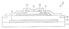
도 1은 종래기술에 따른 산화물 박막 트랜지스터의 개략적인 단면도이다.1 is a schematic cross-sectional view of an oxide thin film transistor according to the prior art.
종래기술에 따른 산화물 박막 트랜지스터(10)는, 도 1에 도시된 바와 같이, 기판(11) 상에 일정 폭과 길이를 갖고 패턴된 게이트전극(13)과, 상기 게이트전극 (13)을 포함한 기판(11) 전면에 형성된 게이트 절연막(15)과, 상기 게이트 전극 (13) 상측을 포함한 게이트 절연막(15)의 상부에 형성되고 일정 모양으로 패턴 형성된 산화물 반도체로 이루어진 액티브층(17)과, 상기 액티브층(17)과 게이트 절연막(15) 상부에 걸쳐 형성된 소스전극(21) 및 드레인전극(23)을 포함하여 구성된다.As shown in FIG. 1, the oxide
여기서, 상기 박막트랜지스터(10)는 식각정지층이 없기 때문에 액티브층(17)이 외부로 노출되므로, 외부 환경 및 식각 조건에 따라 박막트랜지스터 특성이 영향을 받게 된다.Here, since the
따라서, 이렇게 액티브층(17)이 외부로 노출되므로 인해 박막트랜지스터 특성이 영향받게 되는 것을 해결하기 위해 제안한 구조로, 액티브층의 채널영역 상부 에 식각정지층을 배치하는 구조가 제안되었다.Therefore, as a structure proposed to solve the thin film transistor characteristics affected by the
이러한 식각정지층을 구비한 종래기술에 따른 박막트랜지스터 구조에 대해 도 2를 참조하여 설명하면 다음과 같다.A thin film transistor structure according to the related art having such an etch stop layer will be described with reference to FIG. 2 as follows.
도 2는 종래기술에 따른 산화물 박막 트랜지스터의 개략적인 단면도로서, 액티브층의 채널영역 상부에 식각정지층패턴이 배치된 도면이다.2 is a schematic cross-sectional view of an oxide thin film transistor according to the related art, in which an etch stop layer pattern is disposed on a channel region of an active layer.
종래기술에 따른 산화물 박막 트랜지스터(20)는, 도 2에 도시된 바와 같이, 기판(11) 상에 일정 폭과 길이를 갖고 패턴된 게이트전극(13)과, 상기 게이트전극 (13)을 포함한 기판(11) 전면에 형성된 게이트 절연막(15)과, 상기 게이트 전극 (13) 상측을 포함한 게이트 절연막(15)의 상부에 형성되고 일정 모양으로 패턴 형성된 산화물 반도체로 이루어진 액티브층(17)과, 상기 액티브층(17)의 채널영역 상부에 형성된 식각정지층(17)과; 상기 액티브층(17)과 게이트 절연막(15) 상부에 형성되고, 서로 이격된 소스전극(21) 및 드레인전극(23)을 포함하여 구성된다.As shown in FIG. 2, the oxide
여기서, 상기 식각정지층(19)은 상기 게이트전극(13)과 액티브층(17)과 오버랩되어 있으며, 상기 액티브층(17)의 채널영역 상부에 형성된다.The
또한, 상기 소스전극(21) 및 드레인전극(23)은 상기 식각정지층(19) 상부에서 서로 이격되어 형성되고, 상기 식각정지층(19), 액티브층(17) 및 게이트 절연막 (15)에 걸쳐 형성된다.In addition, the
그러나, 종래기술에 따른 산화물 박막트랜지스터 구조에 따르면, 도 2에서와 같이, 액티브층(17)의 안정성(stability) 확보를 위해 식각정지층(19)을 별도로 형성해야 하기 때문에, 상기 식각정지층(19)을 형성하기 위한 별도의 마스크가 추가로 필요하며, 그에 따른 포토 공정 등이 필요하게 된다.However, according to the oxide thin film transistor structure according to the related art, as shown in FIG. 2, since the
따라서, 종래기술에 따른 산화물 박막트랜지스터는 식각정지층의 추가로 인해 요구되는 마스크 및 포토 공정 등이 필요하게 됨으로써, 제조 공정이 복잡해지고 그로 인해 제조 비용이 증가하게 된다.Accordingly, the oxide thin film transistor according to the prior art requires a mask and a photo process required by the addition of the etch stop layer, thereby increasing the manufacturing process and thereby increasing the manufacturing cost.
본 발명은 종래기술의 문제점들을 해결하기 위한 것으로, 본 발명의 목적은 산화물 반도체층 표면에만 합금 산화막(alloy oxide)을 형성하여 산화물 반도체층을 외부 환경으로부터 보호하고, 안정적인 소자 특성을 확보할 수 있는 산화물 박막트랜지스터 및 그 제조방법을 제공함에 있다.The present invention is to solve the problems of the prior art, an object of the present invention is to form an alloy oxide (alloy oxide) only on the oxide semiconductor layer surface to protect the oxide semiconductor layer from the external environment, and to ensure stable device characteristics An oxide thin film transistor and a method of manufacturing the same are provided.
상기 목적을 달성하기 위한 본 발명에 따른 산화물 박막트랜지스터의 제1 특징은, 기판상에 형성된 게이트전극과; 상기 게이트전극을 포함한 기판 전면에 형성된 게이트 절연막과; 상기 게이트전극 상측의 게이트 절연막 상에 형성된 산화물 반도체막으로 이루어진 액티브패턴과; 상기 액티브패턴의 측면 및 상부 표면에 형성된 합금 산화막과; 상기 합금 산화막을 포함한 기판 상에 형성되고, 서로 이격된 소스전극 및 드레인전극;을 포함하여 구성되는 것을 특징으로 한다.A first feature of the oxide thin film transistor according to the present invention for achieving the above object is a gate electrode formed on a substrate; A gate insulating film formed on an entire surface of the substrate including the gate electrode; An active pattern made of an oxide semiconductor film formed on the gate insulating film above the gate electrode; An alloy oxide film formed on side surfaces and top surfaces of the active pattern; And a source electrode and a drain electrode formed on the substrate including the alloy oxide film and spaced apart from each other.
상기 목적을 달성하기 위한 본 발명에 따른 산화물 박막트랜지스터 제조방법은, 기판상에 게이트전극을 형성하는 단계와; 상기 게이트전극을 포함한 기판 전면에 게이트 절연막을 형성하는 단계와; 상기 게이트전극 상측의 게이트 절연막 상에 산화물 반도체막으로 이루어진 액티브패턴을 형성하는 단계와; 상기 액티브패턴 측면 및 상부 표면에 합금 산화막을 형성하는 단계와; 상기 합금 산화막과 게이트절연막 상에 서로 이격된 소스전극과 드레인전극을 형성하는 단계;를 포함하여 구성되는 것을 특징으로 한다.Oxide thin film transistor manufacturing method according to the present invention for achieving the above object comprises the steps of forming a gate electrode on the substrate; Forming a gate insulating film on an entire surface of the substrate including the gate electrode; Forming an active pattern made of an oxide semiconductor film on the gate insulating film above the gate electrode; Forming an alloy oxide film on the side surfaces and the upper surface of the active pattern; And forming a source electrode and a drain electrode spaced apart from each other on the alloy oxide film and the gate insulating film.
본 발명에 따른 산화물 박막트랜지스터 및 그 제조방법에 따르면 다음과 같은 효과가 있다.According to the oxide thin film transistor and the method of manufacturing the same according to the present invention has the following effects.
본 발명에 따른 산화물 박막트랜지스터 및 그 제조방법에 따르면, 산화물 반도체를 액티브층으로 사용하는 박막트랜지스터 구조에서 산화물 반도체층을 증착한 이후에 다시 금속 합금층을 증착하고 이후 열처리를 통해 상기 산화물 반도체층 표면에 합금 산화막을 형성하고 잔류하는 금속 합금층은 식각하여, 자기 정렬 (Self-aligned) 방법으로 산화물 반도체층 표면에만 합금 산화막을 형성함으로써, 산화물 반도체층을 외부 환경으로부터 보호할 수 있으며, 안정적인 소자 특성을 확보할 수 있다.According to the oxide thin film transistor according to the present invention and a method of manufacturing the same, in the thin film transistor structure using the oxide semiconductor as an active layer, after depositing the oxide semiconductor layer, the metal alloy layer is deposited again and then the surface of the oxide semiconductor layer through heat treatment The alloy oxide film is formed on the metal oxide layer, and the remaining metal alloy layer is etched to form the alloy oxide film only on the surface of the oxide semiconductor layer by a self-aligned method, thereby protecting the oxide semiconductor layer from the external environment. Can be secured.
또한, 본 발명에 따른 산화물 박막트랜지스터 및 그 제조방법은 액티브층으로 이용하는 산화물 반도체층의 표면에 자기 정렬 방법으로 합금 산화막을 형성하여 산화물 반도체층을 보호할 수 있기 때문에, 별도의 마스크를 추가하지 않아도 되며, 식각정지층을 별도로 추가하지 않아도 되므로, 그만큼 제조 공정이 단순화되며, 제조비용이 절감된다.In addition, the oxide thin film transistor and the method of manufacturing the same according to the present invention can protect the oxide semiconductor layer by forming an alloy oxide film on the surface of the oxide semiconductor layer used as the active layer by a self-aligning method, so that a separate mask is not required. In addition, since the etch stop layer does not need to be added separately, the manufacturing process is simplified, and the manufacturing cost is reduced.
도 1은 종래기술에 따른 산화물 박막 트랜지스터의 개략적인 단면도이다.
도 2는 종래기술에 따른 산화물 박막 트랜지스터의 개략적인 단면도로서, 액티브층의 채널영역 상부에 식각정지층패턴이 배치된 도면이다.
도 3은 본 발명의 제1 실시 예에 따른 산화물 박막 트랜지스터의 개략적인 단면도이다.
도 4a 내지 4f는 본 발명의 제1 실시 예에 따른 산화물 박막 트랜지스터의 제조공정 단면도들이다.
도 5a 내지 5e는 본 발명의 제1 실시 예에 따른 산화물 박막 트랜지스터의 또 다른 제조 공정 단면도들이다.
도 6은 본 발명의 제2 실시 예에 따른 산화물 박막 트랜지스터의 개략적인 단면도이다.
도 7a 내지 7k는 본 발명의 제2 실시 예에 따른 산화물 박막트랜지스터의 제조 공정 단면도들이다.
도 8은 발명의 제3 실시 예에 따른 산화물 박막트랜지스터의 개략적인 단면도이다.
도 9a 내지 9h는 본 발명의 제3 실시 예에 따른 산화물 박막 트랜지스터의 또 다른 제조 공정 단면도들이다.1 is a schematic cross-sectional view of an oxide thin film transistor according to the prior art.
2 is a schematic cross-sectional view of an oxide thin film transistor according to the related art, in which an etch stop layer pattern is disposed on a channel region of an active layer.
3 is a schematic cross-sectional view of an oxide thin film transistor according to a first exemplary embodiment of the present invention.
4A through 4F are cross-sectional views illustrating a process of manufacturing an oxide thin film transistor according to a first exemplary embodiment of the present invention.
5A to 5E are cross-sectional views illustrating still another manufacturing process of the oxide thin film transistor according to the first embodiment of the present invention.
6 is a schematic cross-sectional view of an oxide thin film transistor according to a second exemplary embodiment of the present invention.
7A to 7K are cross-sectional views illustrating a process of manufacturing an oxide thin film transistor according to a second exemplary embodiment of the present invention.
8 is a schematic cross-sectional view of an oxide thin film transistor according to a third exemplary embodiment of the present invention.
9A to 9H are cross-sectional views illustrating still another manufacturing process of the oxide thin film transistor according to the third embodiment of the present invention.
이하, 본 발명의 바람직한 실시 예에 따른 산화물 박막트랜지스터 구조에 대해 첨부된 도면을 참조하여 상세히 설명한다.Hereinafter, an oxide thin film transistor structure according to a preferred embodiment of the present invention will be described in detail with reference to the accompanying drawings.
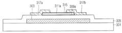
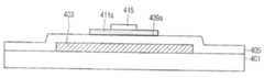
도 3은 본 발명의 제1 실시 예에 따른 산화물 박막 트랜지스터의 개략적인 단면도이다.3 is a schematic cross-sectional view of an oxide thin film transistor according to a first exemplary embodiment of the present invention.
본 발명의 제1 실시 예에 따른 산화물 박막트랜지스터(100)는, 도 3에 도시된 바와 같이, 기판(101)상에 형성된 게이트전극(103)과; 상기 게이트전극(103)을 포함한 기판 전면에 형성된 게이트 절연막(105)과; 상기 게이트전극(103) 상측의 게이트 절연막(105) 상에 형성된 액티브패턴(107)과; 상기 액티브패턴(107)의 표면에 형성된 합금 산화막(alloy oxide)(111)과; 상기 합금 산화막(111)과 게이트절연막(105) 상에 형성되고, 서로 이격된 소스전극(113a) 및 드레인전극(113b)을 포함하여 구성된다.The oxide
여기서, 상기 합금 산화막(111)은 상기 액티브패턴(107)의 측면 및 상부 표면에 형성되어 있다.Here, the
상기 본 발명의 제1 실시 예에 따른 산화물 박막트랜지스터(100)는 탑 게이트(Top gate), 바텀 게이트(Bottom gate) 방식 등을 포함하여 구동 가능한 박막트랜지스터 구조를 모두 포함한다. 또한, 상기 박막트랜지스터(100)는 식각정지층을 사용하는 박막트랜지스터 및 BCE 구조의 박막트랜지스터를 포함한다.The oxide
본 발명에 따른 박막트랜지스터(100)는 액정표시장치 (Liquid Crystal Display; 이하 LCD라 함), 유기발광 다이오드(Organic Luminescence Emitted Diode; 이하 OLED라 함) 등 평판 디스플레이의 구동 소자 또는 스위칭 소자나, 메모리 소자의 주변 회로 구성을 위한 소자 등 다양한 전자 소자에 적용될 수 있다.The
상기 기판(101)은 실리콘, 유리, 플라스틱 또는 다른 적절한 물질을 포함하여 이루어질 수 있다.The
상기 게이트 전극(103)으로는, 알루미늄(Al), 알루미늄 합금(Al alloy), 텅스텐(W), 구리(Cu), Cu 합금, 몰리브덴(Mo), 은(Ag), 은 합금(Ag alloy), 금(Au), 금 합금(Au alloy), 크롬(Cr), 티타늄(Ti), 티타늄 합금(Ti alloy), 몰리텅스텐(MoW), 몰리티타늄 (MoTi), 구리/몰리티타늄 (Cu/MoTi)을 포함하는 도전성 금속 그룹 중에서 선택된 적어도 어느 하나 또는 이들의 2 이상의 조합 또는 다른 적절한 물질을 포함할 수도 있다.As the
또한, 상기 게이트 절연막(105)으로는 실리콘(Si) 계열의 산화막, 질화막, 또는 이를 포함하는 화합물과, Al2O3를 포함하는 금속산화막(metal oxide), 유기절연막, 낮은 유전 상수(low-k) 값을 갖는 재료를 포함한다. 예를 들어, 상기 게이트절연막(107)으로는, 산화실리콘(SiO2), 질화실리콘(SiNx), 산화지르코늄(ZrO2), 산화하프늄(HfO2), 산화티타늄(TiO2), 산화탄탈륨(Ta2O5), 바륨-스트론튬-티타늄-산소화합물(Ba-Sr-Ti-O) 및 비스머스-아연-니오븀-산소 화합물(Bi-Zn-Nb-O)로 이루어지는 그룹으로부터 선택되는 어느 하나 또는 이들의 2 이상의 조합 또는 다른 적절한 물질을 포함할 수도 있다.In addition, the
그리고, 상기 액티브패턴(107)은 소스전극(113a)과 드레인전극(113b) 사이에 전자가 이동하는 채널을 형성하기 위한 층으로서, 저온 다결정 실리콘(Low Temperature Poly Silicon; 이하 LTPS라 함) 또는 비정질 실리콘(a-Si) 재질 대신에 실리콘(Si) 계열의 반도체 막, IGZO 계열의 산화물 반도체막, 화합물 반도체, 카본 나노 튜브(Carbon nano tube), 그라핀(graphene)을 사용한다.The
이때, 상기 산화물 반도체로는, 게르마늄 (Ge), 주석(Sn), 납(Pb), 인듐 (In), 티타늄(Ti), 갈륨(Ga) 및 알루미늄(Al)으로 이루어지는 그룹으로부터 선택된 하나 이상의 물질 및 아연(Zn)을 포함하는 산화물 반도체에 실리콘(Si)이 첨가된 물질로 이루어질 수 있다. 예컨대, 상기 액티브패턴(109a)은 인듐아연 복합 산화물(InZnO)에 실리콘 이온이 첨가된 실리콘 산화인듐아연(Si-InZnO: SIZO)으로 이루어질 수도 있다.In this case, the oxide semiconductor, at least one material selected from the group consisting of germanium (Ge), tin (Sn), lead (Pb), indium (In), titanium (Ti), gallium (Ga) and aluminum (Al). And silicon (Si) added to the oxide semiconductor including zinc (Zn). For example, the active pattern 109a may be formed of silicon indium zinc oxide (Si-InZnO: SIZO) in which silicon ions are added to indium zinc complex oxide (InZnO).
상기 액티브패턴(107)이 SIZO로 이루어지는 경우, 액티브층에서 아연(Zn), 인듐(In) 및 실리콘(Si) 원자의 전체 함량 대비 실리콘(Si) 원자 함량의 조성비는 약 0.001 중량%(wt%) 내지 약 30 wt%일 수도 있다. 실리콘(Si) 원자 함량이 높아질수록 전자 생성을 제어하는 역할이 강해져서, 이동도가 낮아질 수 있으나, 그 소자의 안정성은 더 좋아질 수 있다.When the
한편, 상기 액티브패턴(107)으로는, 전술한 물질 외에 리튬(Li) 또는 칼륨(K)과 같은 I족 원소, 마그네슘(Mg), 칼슘(Ca) 또는 스트론튬(Sr)과 같은 Ⅱ족 원소, 갈륨(Ga), 알루미늄(Al), 인듐(In) 또는 이트륨(Y)과 같은 Ⅲ족 원소, 티타늄(Ti), 지르코늄(Zr), 실리콘(Si), 주석(Sn) 또는 게르마늄(Ge)과 같은 Ⅳ족 원소, 탄탈륨(Ta), 바나듐(V), 니오븀(Nb) 또는 안티몬(Sb)과 같은 Ⅴ족 원소, 또는 란티늄(La), 세륨(Ce), 프라세오디뮴(Pr), 네오디뮴(Nd), 프로메튬(Pm), 사마륨 (Sm), 유로퓸(Eu), 가돌리듐(Gd), 터븀(Tb), 디스프로슘(Dy), 홀뮴(Ho), 어븀(Er), 툴륨(Tm), 이터븀(Yb) 또는 루테듐(Lu)과 같은 란탄(Ln) 계열 원소 등이 더 포함될 수도 있다.Meanwhile, the
상기 합금 산화막(111)은 Cu 합금, Ag 합금, Au 합금, Al 합금을 포함하는 반응성 합금 또는 Ti, Zr, Hf, V, Nb, Ta, Cr, Mo, W, Mn, Fe, Co, Ni 및 이를 포함한 합금 막으로 구성된 금속 중에서 어느 하나를 이용하여 형성될 수 있다.The
더욱이, 상기 소스전극(113a) 및 드레인전극(113b)으로는 알루미늄(Al), 알루미늄 합금(Al alloy), 텅스텐(W), 구리(Cu), 몰리브덴(Mo), 은(Ag), 은 합금(Ag alloy), 금(Au), 금 합금(Au alloy), 크롬(Cr), 티타늄(Ti), 티타늄 합금(Ti alloy), 몰리텅스텐(MoW), 몰리티타늄 (MoTi), 구리/몰리티타늄 (Cu/MoTi)을 포함하는 도전성 금속 그룹 중에서 선택된 적어도 어느 하나 또는 이들의 2 이상의 조합 또는 다른 적절한 물질을 포함할 수도 있다.Further, the
따라서, 본 발명의 제1 실시 예에 따른 산화물 박막트랜지스터에 따르면, 산화물 반도체를 액티브층으로 사용하는 박막트랜지스터 구조에서 산화물 반도체층을 증착한 이후에 다시 금속 합금층을 증착하고 이후 열처리를 통해 상기 산화물 반도체층 표면에 합금 산화막을 형성하고 잔류하는 금속 합금층은 식각하여, 자기 정렬 (Self-aligned) 방법으로 산화물 반도체층 표면에만 합금 산화막을 형성함으로써, 산화물 반도체층을 외부 환경으로부터 보호할 수 있으며, 안정적인 소자 특성을 확보할 수 있다.Therefore, according to the oxide thin film transistor according to the first embodiment of the present invention, in the thin film transistor structure using the oxide semiconductor as an active layer, after depositing the oxide semiconductor layer, the metal alloy layer is deposited again and then the oxide through heat treatment The alloy oxide film is formed on the surface of the semiconductor layer and the remaining metal alloy layer is etched to form the alloy oxide film only on the surface of the oxide semiconductor layer by a self-aligned method, thereby protecting the oxide semiconductor layer from the external environment. Stable device characteristics can be secured.
상기 구성으로 이루어지는 본 발명의 제1 실시 예에 따른 산화물 박막트랜지스터 제조방법에 대해 도 4a 내지 4f를 참조하여 상세히 설명한다.An oxide thin film transistor manufacturing method according to the first embodiment of the present invention having the above configuration will be described in detail with reference to FIGS. 4A to 4F.
도 4a 내지 4f는 본 발명의 제1 실시 예에 따른 산화물 박막 트랜지스터의 제조공정 단면도들이다.4A through 4F are cross-sectional views illustrating a process of manufacturing an oxide thin film transistor according to a first exemplary embodiment of the present invention.
도면에는 도시하지 않았지만, 기판(101)상에 게이트전극용 제1 도전물질을 스퍼터링방법으로 증착하여 제1 도전층(미도시)을 형성하고, 그 위에 제1 감광막(미도시)을 도포한 후, 포토리소그라피 공정기술을 이용한 제1 마스크 공정을 통해 상기 제1 감광막(미도시)을 패터닝하여 제1 감광막패턴(미도시)을 형성한다.Although not shown in the drawing, a first conductive material for a gate electrode is deposited on the
이때, 상기 기판(101)은 실리콘, 유리, 플라스틱 또는 다른 적절한 물질을 포함하여 이루어질 수 있다.In this case, the
또한, 상기 제1 도전층(미도시)으로는, 알루미늄(Al), 알루미늄 합금(Al alloy), 텅스텐(W), 구리(Cu), Cu 합금, 몰리브덴(Mo), 은(Ag), 은 합금(Ag alloy), 금(Au), 금 합금(Au alloy), 크롬(Cr), 티타늄(Ti), 티타늄 합금(Ti alloy), 몰리텅스텐 (MoW), 몰리티타늄 (MoTi), 구리/몰리티타늄 (Cu/MoTi)을 포함하는 도전성 금속 그룹 중에서 선택된 적어도 어느 하나 또는 이들의 2 이상의 조합 또는 다른 적절한 물질을 포함할 수도 있다.In addition, as the first conductive layer (not shown), aluminum (Al), aluminum alloy (Al alloy), tungsten (W), copper (Cu), Cu alloy, molybdenum (Mo), silver (Ag), silver Alloys (Ag), Gold (Au), Au alloys, Chromium (Cr), Titanium (Ti), Titanium alloys (Ti alloys), Molytungsten (MoW), Motitanium (MoTi), Copper / Moli It may also comprise at least any one selected from the group of conductive metals comprising titanium (Cu / MoTi) or a combination of two or more thereof or other suitable materials.
그 다음, 도 4a를 참조하면, 상기 제1 감광막패턴(미도시)을 식각 마스크로 상기 제1 도전층(미도시)을 선택적으로 식각하여 게이트전극(103)을 형성한다.4A, the first conductive layer (not shown) is selectively etched using the first photoresist pattern (not shown) as an etching mask to form a
이어서, 도 4b를 참조하면, 상기 제1 감광막패턴을 제거하고, 상기 게이트전극(103)을 포함한 기판 전면에 게이트 절연막(105)을 형성한다. 이때, 상기 게이트 절연막(105)으로는 실리콘(Si) 계열의 산화막, 질화막, 또는 이를 포함하는 화합물과, Al2O3를 포함하는 금속산화막(metal oxide), 유기절연막, 낮은 유전 상수 (low-k) 값을 갖는 재료를 포함한다. 예를 들어, 상기 게이트절연막(105)으로는, 산화실리콘(SiO2), 질화실리콘(SiNx), 산화지르코늄(ZrO2), 산화하프늄(HfO2), 산화티타늄(TiO2), 산화탄탈륨(Ta2O5), 바륨-스트론튬-티타늄-산소화합물 (Ba-Sr-Ti-O) 및 비스머스-아연-니오븀-산소 화합물(Bi-Zn-Nb-O)로 이루어지는 그룹으로부터 선택되는 어느 하나 또는 이들의 2 이상의 조합 또는 다른 적절한 물질을 포함할 수도 있다.Subsequently, referring to FIG. 4B, the first photoresist layer pattern is removed and a
그 다음, 상기 게이트 절연막(105) 상부에 액티브층(미도시)을 형성한다. 이때, 상기 액티브층은 소스전극(미도시)과 드레인전극(미도시) 사이에 전자가 이동하는 채널을 형성하기 위한 층으로서, 저온 다결정 실리콘(Low Temperature Poly Silicon; 이하 LTPS라 함) 또는 비정질 실리콘(a-Si) 재질 대신에 실리콘(Si) 계열의 반도체 막, IGZO 계열의 산화물 반도체막, 화합물 반도체, 카본 나노 튜브 (Carbon nano tube), 그라핀(graphene)을 사용한다.Next, an active layer (not shown) is formed on the
이때, 상기 산화물 반도체로는, 게르마늄 (Ge), 주석(Sn), 납(Pb), 인듐 (In), 티타늄(Ti), 갈륨(Ga) 및 알루미늄(Al)으로 이루어지는 그룹으로부터 선택된 하나 이상의 물질 및 아연(Zn)을 포함하는 산화물 반도체에 실리콘(Si)이 첨가된 물질로 이루어질 수 있다. 예컨대, 상기 액티브층(미도시)은 인듐아연 복합 산화물 (InZnO)에 실리콘 이온이 첨가된 실리콘 산화인듐아연(Si-InZnO: SIZO)으로 이루어질 수도 있다.In this case, the oxide semiconductor, at least one material selected from the group consisting of germanium (Ge), tin (Sn), lead (Pb), indium (In), titanium (Ti), gallium (Ga) and aluminum (Al). And silicon (Si) added to the oxide semiconductor including zinc (Zn). For example, the active layer (not shown) may be made of silicon indium zinc oxide (Si-InZnO: SIZO) in which silicon ions are added to indium zinc complex oxide (InZnO).
상기 액티브층(미도시)이 SIZO로 이루어지는 경우, 액티브층에서 아연(Zn), 인듐(In) 및 실리콘(Si) 원자의 전체 함량 대비 실리콘(Si) 원자 함량의 조성비는 약 0.001 중량%(wt%) 내지 약 30 wt%일 수도 있다. 실리콘(Si) 원자 함량이 높아질수록 전자 생성을 제어하는 역할이 강해져서, 이동도가 낮아질 수 있으나, 그 소자의 안정성은 더 좋아질 수 있다.When the active layer (not shown) is made of SIZO, the composition ratio of the silicon (Si) atomic content to the total content of zinc (Zn), indium (In), and silicon (Si) atoms in the active layer is about 0.001% by weight (wt %) To about 30 wt%. The higher the silicon (Si) atomic content, the stronger the role of controlling electron generation, so that the mobility may be lowered, but the stability of the device may be better.
한편, 상기 액티브층(미도시)으로는, 전술한 물질 외에 리튬(Li) 또는 칼륨(K)과 같은 I족 원소, 마그네슘(Mg), 칼슘(Ca) 또는 스트론튬(Sr)과 같은 Ⅱ족 원소, 갈륨(Ga), 알루미늄(Al), 인듐(In) 또는 이트륨(Y)과 같은 Ⅲ족 원소, 티타늄(Ti), 지르코늄(Zr), 실리콘(Si), 주석(Sn) 또는 게르마늄(Ge)과 같은 Ⅳ족 원소, 탄탈륨 (Ta), 바나듐(V), 니오븀(Nb) 또는 안티몬(Sb)과 같은 Ⅴ족 원소, 또는 란티늄 (La), 세륨(Ce), 프라세오디뮴(Pr), 네오디뮴(Nd), 프로메튬(Pm), 사마륨 (Sm), 유로퓸(Eu), 가돌리듐(Gd), 터븀(Tb), 디스프로슘(Dy), 홀뮴(Ho), 어븀(Er), 툴륨 (Tm), 이터븀(Yb) 또는 루테듐(Lu)과 같은 란탄(Ln) 계열 원소 등이 더 포함될 수도 있다.On the other hand, the active layer (not shown), in addition to the above-described materials, Group I elements such as lithium (Li) or potassium (K), Group II elements such as magnesium (Mg), calcium (Ca) or strontium (Sr) , Group III elements such as gallium (Ga), aluminum (Al), indium (In) or yttrium (Y), titanium (Ti), zirconium (Zr), silicon (Si), tin (Sn) or germanium (Ge) Group IV elements such as tantalum (Ta), vanadium (V), niobium (Nb) or antimony (Sb), or Group V elements such as lanthanum (La), cerium (Ce), praseodymium (Pr), and neodymium ( Nd, Promethium (Pm), Samarium (Sm), Europium (Eu), Gadolinium (Gd), Terbium (Tb), Dysprosium (Dy), Holmium (Ho), Erbium (Er), Thulium (Tm), Eater A lanthanum (Ln) based element such as tungsten (Yb) or ruthedium (Lu) may be further included.
이어서, 도면에는 도시하지 않았지만, 상기 액티브층(미도시) 상에 제2 감광막(미도시)을 도포한 후, 포토리소그라피 공정기술을 이용한 제2 마스크 공정을 통해 상기 제2 감광막(미도시)을 노광 및 현상한 후 상기 제2 감광막(미도시)을 선택적으로 패터닝하여 제2 감광막패턴(미도시)을 형성한다.Subsequently, although not shown in the drawings, a second photosensitive film (not shown) is coated on the active layer (not shown), and then the second photosensitive film (not shown) is applied through a second mask process using a photolithography process technology. After exposure and development, the second photoresist layer (not shown) is selectively patterned to form a second photoresist layer pattern (not shown).
그 다음, 상기 제2 감광막패턴(미도시)을 식각마스크로, 상기 액티브층(미도시)을 선택적으로 식각하여 액티브패턴(107)을 형성한다.Next, the second photoresist layer pattern (not shown) is used as an etching mask, and the active layer (not shown) is selectively etched to form an
이어서, 도 4c를 참조하면, 상기 액티브패턴(107) 상에 반응성 금속층(109)을 형성한다. 이때, 상기 반응성 금속층(109)은 액티브층을 구성하는 산화물 반도체를 증착하기 전에 게이트절연막(105)의 표면을 개선하기 위해 사용할 수도 있다.4C, a
상기 반응성 금속층(109)은 Cu 합금, Ag 합금, Au 합금, Al 합금을 포함하는 반응성 합금 또는 Ti, Zr, Hf, V, Nb, Ta, Cr, Mo, W, Mn, Fe, Co, Ni 및 이를 포함한 합금 막으로 구성된 금속 중에서 어느 하나를 이용하여 형성될 수 있다. 이때, 상기 합금 원소는 Ca, Mg, Zn, Al, Zr, V, Nb, Ta, Cr, Mo, W, Mn, Fe, Ru, Co, Ni, Ag, Au, Zn 을 포함한다.The
그 다음, 아닐링 공정을 실시하여, 상기 반응성 금속층(109)과 접촉하는 상기 액티브층(107)의 계면에 합금 산화막(alloy oxide) (111)을 형성한다. 이때, 상기 아닐링 공정은 상압, 진공 아닐링(annealing) 방법을 모두 포함하며, 열원으로는 광원으로 이용하는 방법도 모두 포함할 수 있다. 이때, 상기 합금 산화막(111)은 자기 정렬(Self-aligned) 방법으로 형성된다고 볼 수 있다.Then, an annealing process is performed to form an
이어서, 도 4d를 참조하면, 상기 반응성 금속층(109)을 습식 식각 방법을 통해 제거하여, 상기 합금 산화막(111)과 게이트절연막(105)을 외부로 노출시킨다.Next, referring to FIG. 4D, the
그 다음, 도 4e를 참조하면, 외부로 노출된 상기 합금산화막(111) 및 게이트절연막(105) 상에 제2 도전층(113)을 스퍼터링 방법으로 증착하여 형성한다. 이때, 상기 제2 도전층(113)으로는, 알루미늄(Al), 알루미늄 합금(Al alloy), 텅스텐 (W), 구리(Cu), Cu 합금, 몰리브덴(Mo), 은(Ag), 은 합금(Ag alloy), 금(Au), 금 합금(Au alloy), 크롬(Cr), 티타늄(Ti), 티타늄 합금(Ti alloy), 몰리텅스텐 (MoW), 몰리티타늄 (MoTi), 구리/몰리티타늄 (Cu/MoTi)을 포함하는 도전성 금속 그룹 중에서 선택된 적어도 어느 하나 또는 이들의 2 이상의 조합 또는 다른 적절한 물질을 포함할 수도 있다. Next, referring to FIG. 4E, a second
이어서, 상기 제2 도전층(113) 상에 제3 감광막(미도시)을 도포한 후 포토리소그라피 공정기술을 이용한 제3 마스크 공정을 통해 상기 제3 감광막(미도시)을 노광 및 현상한 후 상기 제3 감광막(미도시)을 선택적으로 패터닝하여 제3 감광막패턴(미도시)을 형성한다.Subsequently, after applying a third photoresist film (not shown) on the second
그 다음, 도 4f를 참조하면, 상기 제3 감광막패턴(미도시)을 식각마스크로, 상기 제2 도전층(113)을 식각하여, 상기 이격된 소스전극(113a) 및 드레인전극 (113b)을 형성하고 제3 감광막패턴(미도시)을 제거함으로써, 본 발명의 제1 실시 예에 따른 산화물 박막트랜지스터 제조공정을 완료한다.Next, referring to FIG. 4F, the second
따라서, 본 발명에 따른 산화물 박막트랜지스터 제조방법에 따르면, 산화물 반도체를 액티브층으로 사용하는 박막트랜지스터 구조에서 산화물 반도체층을 증착한 이후에 다시 금속 합금층을 증착하고 이후 열처리를 통해 상기 산화물 반도체층 표면에 합금 산화막을 형성하고 잔류하는 금속 합금층은 식각하여, 자기 정렬 (Self-aligned) 방법으로 산화물 반도체층 표면에만 합금 산화막을 형성함으로써, 산화물 반도체층을 외부 환경으로부터 보호할 수 있으며, 안정적인 소자 특성을 확보할 수 있다.Accordingly, according to the method of manufacturing an oxide thin film transistor according to the present invention, in the thin film transistor structure using the oxide semiconductor as an active layer, the metal alloy layer is deposited again after the oxide semiconductor layer is deposited, and then the surface of the oxide semiconductor layer through heat treatment. The alloy oxide film is formed on the metal oxide layer, and the remaining metal alloy layer is etched to form the alloy oxide film only on the surface of the oxide semiconductor layer by a self-aligned method, thereby protecting the oxide semiconductor layer from the external environment. Can be secured.
또한, 본 발명에 따른 산화물 박막트랜지스터 제조방법은 액티브층으로 이용하는 산화물 반도체층의 표면에 자기 정렬 방법으로 합금 산화막을 형성하여 산화물 반도체층을 보호할 수 있기 때문에, 별도의 마스크를 추가하지 않아도 되며, 식각정지층을 별도로 추가하지 않아도 되므로, 그만큼 제조 공정이 단순화되며, 제조비용이 절감된다.In addition, in the method of manufacturing the oxide thin film transistor according to the present invention, since the oxide semiconductor layer can be protected by forming an alloy oxide film on the surface of the oxide semiconductor layer used as the active layer, it is not necessary to add a separate mask. Since the etch stop layer does not need to be added separately, the manufacturing process is simplified, and the manufacturing cost is reduced.
한편, 본 발명의 제1 실시 예에 따른 산화물 박막트랜지스터 제조방법의 또다른 제조방법에 대해 도 5a 내지 5e를 참조하여 설명하면 다음과 같다.Meanwhile, another manufacturing method of the oxide thin film transistor manufacturing method according to the first embodiment of the present invention will be described with reference to FIGS. 5A to 5E.
도 5a 내지 5e는 본 발명의 제1 실시 예에 따른 산화물 박막 트랜지스터의 또 다른 제조공정 단면도들이다.5A to 5E are cross-sectional views illustrating still another manufacturing process of the oxide thin film transistor according to the first embodiment of the present invention.
도면에는 도시하지 않았지만, 기판(201)상에 게이트전극용 제1 도전물질을 스퍼터링방법으로 증착하여 제1 도전층(미도시)을 형성하고, 그 위에 제1 감광막(미도시)을 도포한 후, 포토리소그라피 공정기술을 이용한 제1 마스크 공정을 통해 상기 제1 감광막(미도시)을 패터닝하여 제1 감광막패턴(미도시)을 형성한다.Although not shown in the drawing, a first conductive material for a gate electrode is deposited on the
이때, 상기 기판(201)은 실리콘, 유리, 플라스틱 또는 다른 적절한 물질을 포함하여 이루어질 수 있다.In this case, the
또한, 상기 제1 도전층(미도시)으로는, 알루미늄(Al), 알루미늄 합금(Al alloy), 텅스텐(W), 구리(Cu), Cu 합금, 몰리브덴(Mo), 은(Ag), 은 합금(Ag alloy), 금(Au), 금 합금(Au alloy), 크롬(Cr), 티타늄(Ti), 티타늄 합금(Ti alloy), 몰리텅스텐 (MoW), 몰리티타늄 (MoTi), 구리/몰리티타늄 (Cu/MoTi)을 포함하는 도전성 금속 그룹 중에서 선택된 적어도 어느 하나 또는 이들의 2 이상의 조합 또는 다른 적절한 물질을 포함할 수도 있다.In addition, as the first conductive layer (not shown), aluminum (Al), aluminum alloy (Al alloy), tungsten (W), copper (Cu), Cu alloy, molybdenum (Mo), silver (Ag), silver Alloys (Ag), Gold (Au), Au alloys, Chromium (Cr), Titanium (Ti), Titanium alloys (Ti alloys), Molytungsten (MoW), Motitanium (MoTi), Copper / Moli It may also comprise at least any one selected from the group of conductive metals comprising titanium (Cu / MoTi) or a combination of two or more thereof or other suitable materials.
그 다음, 도 5a를 참조하면, 상기 제1 감광막패턴(미도시)을 식각 마스크로 상기 제1 도전층(미도시)을 선택적으로 식각하여 게이트전극(203)을 형성한다.Next, referring to FIG. 5A, the first conductive layer (not shown) is selectively etched using the first photoresist pattern (not shown) as an etching mask to form a
이어서, 도 5b를 참조하면, 상기 제1 감광막패턴을 제거하고, 상기 게이트전극(103)을 포함한 기판 전면에 게이트 절연막(205)을 형성한다. 이때, 상기 게이트 절연막(205)으로는 실리콘(Si) 계열의 산화막, 질화막, 또는 이를 포함하는 화합물과, Al2O3를 포함하는 금속산화막(metal oxide), 유기절연막, 낮은 유전 상수 (low-k) 값을 갖는 재료를 포함한다. 예를 들어, 상기 게이트절연막(205)으로는, 산화실리콘(SiO2), 질화실리콘(SiNx), 산화지르코늄(ZrO2), 산화하프늄(HfO2), 산화티타늄(TiO2), 산화탄탈륨(Ta2O5), 바륨-스트론튬-티타늄-산소화합물 (Ba-Sr-Ti-O) 및 비스머스-아연-니오븀-산소 화합물(Bi-Zn-Nb-O)로 이루어지는 그룹으로부터 선택되는 어느 하나 또는 이들의 2 이상의 조합 또는 다른 적절한 물질을 포함할 수도 있다.Subsequently, referring to FIG. 5B, the first photoresist layer pattern is removed and a
그 다음, 상기 게이트 절연막(205) 상부에 액티브층(미도시)을 형성한다. 이때, 상기 액티브층은 소스전극(미도시)과 드레인전극(미도시) 사이에 전자가 이동하는 채널을 형성하기 위한 층으로서, 저온 다결정 실리콘(Low Temperature Poly Silicon; 이하 LTPS라 함) 또는 비정질 실리콘(a-Si) 재질 대신에 실리콘(Si) 계열의 반도체 막, IGZO 계열의 산화물 반도체막, 화합물 반도체, 카본 나노 튜브 (Carbon nano tube), 그라핀(graphene)을 사용한다.Next, an active layer (not shown) is formed on the
이때, 상기 산화물 반도체로는, 게르마늄 (Ge), 주석(Sn), 납(Pb), 인듐 (In), 티타늄(Ti), 갈륨(Ga) 및 알루미늄(Al)으로 이루어지는 그룹으로부터 선택된 하나 이상의 물질 및 아연(Zn)을 포함하는 산화물 반도체에 실리콘(Si)이 첨가된 물질로 이루어질 수 있다. 예컨대, 상기 액티브층(109)은 인듐아연 복합 산화물 (InZnO)에 실리콘 이온이 첨가된 실리콘 산화인듐아연(Si-InZnO: SIZO)으로 이루어질 수도 있다.In this case, the oxide semiconductor, at least one material selected from the group consisting of germanium (Ge), tin (Sn), lead (Pb), indium (In), titanium (Ti), gallium (Ga) and aluminum (Al). And silicon (Si) added to the oxide semiconductor including zinc (Zn). For example, the
상기 액티브층(미도시)이 SIZO로 이루어지는 경우, 액티브층에서 아연(Zn), 인듐(In) 및 실리콘(Si) 원자의 전체 함량 대비 실리콘(Si) 원자 함량의 조성비는 약 0.001 중량%(wt%) 내지 약 30 wt%일 수도 있다. 실리콘(Si) 원자 함량이 높아질수록 전자 생성을 제어하는 역할이 강해져서, 이동도가 낮아질 수 있으나, 그 소자의 안정성은 더 좋아질 수 있다.When the active layer (not shown) is made of SIZO, the composition ratio of the silicon (Si) atomic content to the total content of zinc (Zn), indium (In), and silicon (Si) atoms in the active layer is about 0.001% by weight (wt %) To about 30 wt%. The higher the silicon (Si) atomic content, the stronger the role of controlling electron generation, so that the mobility may be lowered, but the stability of the device may be better.
한편, 상기 액티브층(미도시)으로는, 전술한 물질 외에 리튬(Li) 또는 칼륨(K)과 같은 I족 원소, 마그네슘(Mg), 칼슘(Ca) 또는 스트론튬(Sr)과 같은 Ⅱ족 원소, 갈륨(Ga), 알루미늄(Al), 인듐(In) 또는 이트륨(Y)과 같은 Ⅲ족 원소, 티타늄(Ti), 지르코늄(Zr), 실리콘(Si), 주석(Sn) 또는 게르마늄(Ge)과 같은 Ⅳ족 원소, 탄탈륨 (Ta), 바나듐(V), 니오븀(Nb) 또는 안티몬(Sb)과 같은 Ⅴ족 원소, 또는 란티늄 (La), 세륨(Ce), 프라세오디뮴(Pr), 네오디뮴(Nd), 프로메튬(Pm), 사마륨 (Sm), 유로퓸(Eu), 가돌리듐(Gd), 터븀(Tb), 디스프로슘(Dy), 홀뮴(Ho), 어븀(Er), 툴륨 (Tm), 이터븀(Yb) 또는 루테듐(Lu)과 같은 란탄(Ln) 계열 원소 등이 더 포함될 수도 있다.On the other hand, the active layer (not shown), in addition to the above-described materials, Group I elements such as lithium (Li) or potassium (K), Group II elements such as magnesium (Mg), calcium (Ca) or strontium (Sr) , Group III elements such as gallium (Ga), aluminum (Al), indium (In) or yttrium (Y), titanium (Ti), zirconium (Zr), silicon (Si), tin (Sn) or germanium (Ge) Group IV elements such as tantalum (Ta), vanadium (V), niobium (Nb) or antimony (Sb), or Group V elements such as lanthanum (La), cerium (Ce), praseodymium (Pr), and neodymium ( Nd, Promethium (Pm), Samarium (Sm), Europium (Eu), Gadolinium (Gd), Terbium (Tb), Dysprosium (Dy), Holmium (Ho), Erbium (Er), Thulium (Tm), Eater A lanthanum (Ln) based element such as tungsten (Yb) or ruthedium (Lu) may be further included.
이어서, 도면에는 도시하지 않았지만, 상기 액티브층(미도시) 상에 제2 감광막(미도시)을 도포한 후, 포토리소그라피 공정기술을 이용한 제2 마스크 공정을 통해 상기 제2 감광막(미도시)을 노광 및 현상한 후 상기 제2 감광막(미도시)을 선택적으로 패터닝하여 제2 감광막패턴(미도시)을 형성한다.Subsequently, although not shown in the drawings, a second photosensitive film (not shown) is coated on the active layer (not shown), and then the second photosensitive film (not shown) is applied through a second mask process using a photolithography process technology. After exposure and development, the second photoresist layer (not shown) is selectively patterned to form a second photoresist layer pattern (not shown).
그 다음, 상기 제2 감광막패턴(미도시)을 식각마스크로, 상기 액티브층(미도시)을 선택적으로 식각하여 액티브패턴(207)을 형성한다.Next, the
이어서, 도 5c를 참조하면, 상기 액티브패턴(207) 상에 반응성 금속층(209)을 형성한다. 이때, 상기 반응성 금속층(209)은 액티브층을 구성하는 산화물 반도체를 증착하기 전에 게이트절연막(105)의 표면을 개선하기 위해 사용할 수도 있다.Subsequently, referring to FIG. 5C, a
상기 반응성 금속층(209)은 Cu 합금, Ag 합금, Au 합금, Al 합금을 포함하는 반응성 합금 또는 Ti, Zr, Hf, V, Nb, Ta, Cr, Mo, W, Mn, Fe, Co, Ni 및 이를 포함한 합금 막으로 구성된 금속 중에서 어느 하나를 이용하여 형성될 수 있다. 이때, 상기 합금 원소는 Ca, Mg, Zn, Al, Zr, V, Nb, Ta, Cr, Mo, W, Mn, Fe, Ru, Co, Ni, Ag, Au, Zn 을 포함한다.The
그 다음, 도 5d를 참조하면, 아닐링 공정을 실시하여 상기 반응성 금속층 (209)과 접촉하는 상기 액티브패턴(207)의 계면에 합금산화막(alloy oxide) (211)을 형성한다. 이때, 상기 아닐링 공정은 상압, 진공 아닐링(annealing) 방법을 모두 포함하며, 열원으로는 광원으로 이용하는 방법도 모두 포함할 수 있다. 이때, 상기 합금산화막 (211)은 자기 정렬(Self-aligned) 방법으로 형성된다고 볼 수 있다.Next, referring to FIG. 5D, an annealing process is performed to form an
이어서, 상기 반응성 금속층(209) 상에 제3 감광막(미도시)을 도포한 후 포토리소그라피 공정기술을 이용한 제3 마스크 공정을 통해 상기 제3 감광막(미도시)을 노광 및 현상한 후 상기 제3 감광막(미도시)을 선택적으로 패터닝하여 제3 감광막패턴(미도시)을 형성한다.Subsequently, after applying a third photoresist film (not shown) on the
그 다음, 도 5e를 참조하면, 상기 제3 감광막패턴(미도시)을 식각마스크로, 상기 반응성 금속층(209)을 식각하여, 상기 이격된 소스전극(209a) 및 드레인전극 (209b)을 형성하고 제3 감광막패턴(미도시)을 제거함으로써, 본 발명의 제1 실시 예에 따른 산화물 박막트랜지스터 제조공정을 완료한다.Next, referring to FIG. 5E, the
따라서, 본 발명에 따른 산화물 박막트랜지스터 제조방법에 따르면, 산화물 반도체를 액티브층으로 사용하는 박막트랜지스터 구조에서 산화물 반도체층을 증착한 이후에 다시 금속 합금층을 증착하고 이후 열처리를 통해 상기 산화물 반도체층 표면에 합금 산화막을 형성하고 잔류하는 금속 합금층은 식각하여, 자기 정렬 (Self-aligned) 방법으로 산화물 반도체층 표면에만 합금 산화막을 형성함으로써, 산화물 반도체층을 외부 환경으로부터 보호할 수 있으며, 안정적인 소자 특성을 확보할 수 있다.Accordingly, according to the method of manufacturing an oxide thin film transistor according to the present invention, in the thin film transistor structure using the oxide semiconductor as an active layer, the metal alloy layer is deposited again after the oxide semiconductor layer is deposited, and then the surface of the oxide semiconductor layer through heat treatment. The alloy oxide film is formed on the metal oxide layer, and the remaining metal alloy layer is etched to form the alloy oxide film only on the surface of the oxide semiconductor layer by a self-aligned method, thereby protecting the oxide semiconductor layer from the external environment. Can be secured.
또한, 본 발명에 따른 산화물 박막트랜지스터 제조방법은 액티브층으로 이용하는 산화물 반도체층의 표면에 자기 정렬 방법으로 합금 산화막을 형성하여 산화물 반도체층을 보호할 수 있기 때문에, 별도의 마스크를 추가하지 않아도 되며, 식각정지층을 별도로 추가하지 않아도 되므로, 그만큼 제조 공정이 단순화되며, 제조비용이 절감된다.In addition, in the method of manufacturing the oxide thin film transistor according to the present invention, since the oxide semiconductor layer can be protected by forming an alloy oxide film on the surface of the oxide semiconductor layer used as the active layer, it is not necessary to add a separate mask. Since the etch stop layer does not need to be added separately, the manufacturing process is simplified, and the manufacturing cost is reduced.
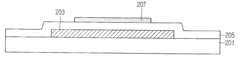
또 한편, 본 발명의 제2 실시 예에 따른 산화물 박막트랜지스터 구조에 대해 도 6을 참조하여 설명하면 다음과 같다.On the other hand, the oxide thin film transistor structure according to the second embodiment of the present invention will be described with reference to FIG.
도 6은 본 발명의 제2 실시 예에 따른 산화물 박막 트랜지스터의 개략적인 단면도이다.6 is a schematic cross-sectional view of an oxide thin film transistor according to a second exemplary embodiment of the present invention.
본 발명의 제2 실시 예에 따른 산화물 박막트랜지스터(300)는, 도 6에 도시된 바와 같이, 기판(301)상에 형성된 게이트전극(303)과; 상기 게이트전극(303)을 포함한 기판 전면에 형성된 게이트 절연막(305)과; 상기 게이트전극(303) 상측의 게이트 절연막(305) 상에 형성된 액티브패턴(311a)과; 상기 액티브패턴(311a)의 표면 전체에 형성된 합금 산화막(alloy oxide)(309a, 315)과; 상기 합금 산화막 (309a, 315)과 게이트절연막(305) 상에 형성되고, 서로 이격된 소스전극(317a) 및 드레인전극(317b)을 포함하여 구성된다.The oxide
여기서, 상기 합금 산화막(309a, 315)은 상기 게이트절연막(305)과 접촉하는 상기 액티브패턴(311a)의 하부 표면에 형성된 제1 합금 산화막(309a)과, 상기 액티브패턴(311a)의 측면 및 상부 표면에 형성된 제2 합금 산화막(315)으로 구성된다.Here, the
상기 본 발명의 제2 실시 예에 따른 산화물 박막트랜지스터(300)는 탑 게이트(Top gate), 바텀 게이트(Bottom gate) 방식 등을 포함하여 구동 가능한 박막트랜지스터 구조를 모두 포함한다. 또한, 상기 박막트랜지스터(200)는 식각정지층을 사용하는 박막트랜지스터 및 BCE 구조의 박막트랜지스터를 포함한다.The oxide
본 발명에 따른 박막트랜지스터(300)는 액정표시장치 (Liquid Crystal Display; 이하 LCD라 함), 유기발광 다이오드(Organic Luminescence Emitted Diode; 이하 OLED라 함) 등 평판 디스플레이의 구동 소자 또는 스위칭 소자나, 메모리 소자의 주변 회로 구성을 위한 소자 등 다양한 전자 소자에 적용될 수 있다.The
상기 기판(301)은 실리콘, 유리, 플라스틱 또는 다른 적절한 물질을 포함하여 이루어질 수 있다.The
상기 게이트 전극(303)으로는, 알루미늄(Al), 알루미늄 합금(Al alloy), 텅스텐(W), 구리(Cu), Cu 합금, 몰리브덴(Mo), 은(Ag), 은 합금(Ag alloy), 금(Au), 금 합금(Au alloy), 크롬(Cr), 티타늄(Ti), 티타늄 합금(Ti alloy), 몰리텅스텐(MoW), 몰리티타늄 (MoTi), 구리/몰리티타늄 (Cu/MoTi)을 포함하는 도전성 금속 그룹 중에서 선택된 적어도 어느 하나 또는 이들의 2 이상의 조합 또는 다른 적절한 물질을 포함할 수도 있다.As the
또한, 상기 게이트 절연막(305)으로는 실리콘(Si) 계열의 산화막, 질화막, 또는 이를 포함하는 화합물과, Al2O3를 포함하는 금속산화막(metal oxide), 유기절연막, 낮은 유전 상수(low-k) 값을 갖는 재료를 포함한다. 예를 들어, 상기 게이트절연막(107)으로는, 산화실리콘(SiO2), 질화실리콘(SiNx), 산화지르코늄(ZrO2), 산화하프늄(HfO2), 산화티타늄(TiO2), 산화탄탈륨(Ta2O5), 바륨-스트론튬-티타늄-산소화합물(Ba-Sr-Ti-O) 및 비스머스-아연-니오븀-산소 화합물(Bi-Zn-Nb-O)로 이루어지는 그룹으로부터 선택되는 어느 하나 또는 이들의 2 이상의 조합 또는 다른 적절한 물질을 포함할 수도 있다.In addition, the
그리고, 상기 액티브패턴(311a)은 소스전극(317a)과 드레인전극(317b) 사이에 전자가 이동하는 채널을 형성하기 위한 층으로서, 저온 다결정 실리콘(Low Temperature Poly Silicon; 이하 LTPS라 함) 또는 비정질 실리콘(a-Si) 재질 대신에 실리콘(Si) 계열의 반도체 막, IGZO 계열의 산화물 반도체막, 화합물 반도체, 카본 나노 튜브(Carbon nano tube), 그라핀(graphene)을 사용한다.In addition, the
이때, 상기 산화물 반도체로는, 게르마늄 (Ge), 주석(Sn), 납(Pb), 인듐 (In), 티타늄(Ti), 갈륨(Ga) 및 알루미늄(Al)으로 이루어지는 그룹으로부터 선택된 하나 이상의 물질 및 아연(Zn)을 포함하는 산화물 반도체에 실리콘(Si)이 첨가된 물질로 이루어질 수 있다. 예컨대, 상기 액티브패턴(109a)은 인듐아연 복합 산화물(InZnO)에 실리콘 이온이 첨가된 실리콘 산화인듐아연(Si-InZnO: SIZO)으로 이루어질 수도 있다.In this case, the oxide semiconductor, at least one material selected from the group consisting of germanium (Ge), tin (Sn), lead (Pb), indium (In), titanium (Ti), gallium (Ga) and aluminum (Al). And silicon (Si) added to the oxide semiconductor including zinc (Zn). For example, the active pattern 109a may be formed of silicon indium zinc oxide (Si-InZnO: SIZO) in which silicon ions are added to indium zinc complex oxide (InZnO).
상기 액티브패턴(311a)이 SIZO로 이루어지는 경우, 액티브층에서 아연(Zn), 인듐(In) 및 실리콘(Si) 원자의 전체 함량 대비 실리콘(Si) 원자 함량의 조성비는 약 0.001 중량%(wt%) 내지 약 30 wt%일 수도 있다. 실리콘(Si) 원자 함량이 높아질수록 전자 생성을 제어하는 역할이 강해져서, 이동도가 낮아질 수 있으나, 그 소자의 안정성은 더 좋아질 수 있다.When the
한편, 상기 액티브패턴(311a)으로는, 전술한 물질 외에 리튬(Li) 또는 칼륨(K)과 같은 I족 원소, 마그네슘(Mg), 칼슘(Ca) 또는 스트론튬(Sr)과 같은 Ⅱ족 원소, 갈륨(Ga), 알루미늄(Al), 인듐(In) 또는 이트륨(Y)과 같은 Ⅲ족 원소, 티타늄(Ti), 지르코늄(Zr), 실리콘(Si), 주석(Sn) 또는 게르마늄(Ge)과 같은 Ⅳ족 원소, 탄탈륨(Ta), 바나듐(V), 니오븀(Nb) 또는 안티몬(Sb)과 같은 Ⅴ족 원소, 또는 란티늄(La), 세륨(Ce), 프라세오디뮴(Pr), 네오디뮴(Nd), 프로메튬(Pm), 사마륨 (Sm), 유로퓸(Eu), 가돌리듐(Gd), 터븀(Tb), 디스프로슘(Dy), 홀뮴(Ho), 어븀(Er), 툴륨(Tm), 이터븀(Yb) 또는 루테듐(Lu)과 같은 란탄(Ln) 계열 원소 등이 더 포함될 수도 있다.On the other hand, as the
상기 제1, 2 합금 산화막(309a, 315)은 Cu 합금, Ag 합금, Au 합금, Al 합금을 포함하는 반응성 합금 또는 Ti, Zr, Hf, V, Nb, Ta, Cr, Mo, W, Mn, Fe, Co, Ni 및 이를 포함한 합금 막으로 구성된 금속 중에서 어느 하나를 이용하여 형성될 수 있다.The first and second
더욱이, 상기 소스전극(317a) 및 드레인전극(317b)으로는 알루미늄(Al), 알루미늄 합금(Al alloy), 텅스텐(W), 구리(Cu), Cu 합금, 몰리브덴(Mo), 은(Ag), 은 합금(Ag alloy), 금(Au), 금 합금(Au alloy), 크롬(Cr), 티타늄(Ti), 티타늄 합금(Ti alloy), 몰리텅스텐(MoW), 몰리티타늄 (MoTi), 구리/몰리티타늄 (Cu/MoTi)을 포함하는 도전성 금속 그룹 중에서 선택된 적어도 어느 하나 또는 이들의 2 이상의 조합 또는 다른 적절한 물질을 포함할 수도 있다.Further, the
따라서, 본 발명의 제2 실시 예에 따른 산화물 박막트랜지스터에 따르면, 산화물 반도체를 액티브층으로 사용하는 박막트랜지스터 구조에서 산화물 반도체층을 증착한 이후에 다시 금속 합금층을 증착하고 이후 열처리를 통해 상기 산화물 반도체층 표면에 합금 산화막을 형성하고 잔류하는 금속 합금층은 식각하여, 자기 정렬 (Self-aligned) 방법으로 산화물 반도체층 표면에만 합금 산화막을 형성함으로써, 산화물 반도체층을 외부 환경으로부터 보호할 수 있으며, 안정적인 소자 특성을 확보할 수 있다.Therefore, according to the oxide thin film transistor according to the second embodiment of the present invention, in the thin film transistor structure using the oxide semiconductor as an active layer, after depositing the oxide semiconductor layer, the metal alloy layer is deposited again and then the oxide through heat treatment The alloy oxide film is formed on the surface of the semiconductor layer and the remaining metal alloy layer is etched to form the alloy oxide film only on the surface of the oxide semiconductor layer by a self-aligned method, thereby protecting the oxide semiconductor layer from the external environment. Stable device characteristics can be secured.
상기 구성으로 이루어지는 본 발명의 제2 실시 예에 따른 산화물 박막트랜지스터 제조방법에 대해 도 7a 내지 7k를 참조하여 상세히 설명한다.An oxide thin film transistor manufacturing method according to a second exemplary embodiment of the present invention having the above configuration will be described in detail with reference to FIGS. 7A to 7K.
도 7a 내지 7k는 본 발명의 제2 실시 예에 따른 산화물 박막 트랜지스터의 제조공정 단면도들이다.7A to 7K are cross-sectional views illustrating a process of manufacturing an oxide thin film transistor according to a second exemplary embodiment of the present invention.
도면에는 도시하지 않았지만, 기판(301)상에 게이트전극용 제1 도전물질을 스퍼터링방법으로 증착하여 제1 도전층(미도시)을 형성하고, 그 위에 제1 감광막(미도시)을 도포한 후, 포토리소그라피 공정기술을 이용한 제1 마스크 공정을 통해 상기 제1 감광막(미도시)을 패터닝하여 제1 감광막패턴(미도시)을 형성한다.Although not shown in the drawing, a first conductive material for a gate electrode is deposited on the
이때, 상기 기판(301)은 실리콘, 유리, 플라스틱 또는 다른 적절한 물질을 포함하여 이루어질 수 있다.In this case, the
또한, 상기 제1 도전층(미도시)으로는, 알루미늄(Al), 알루미늄 합금(Al alloy), 텅스텐(W), 구리(Cu), Cu 합금, 몰리브덴(Mo), 은(Ag), 은 합금(Ag alloy), 금(Au), 금 합금(Au alloy), 크롬(Cr), 티타늄(Ti), 티타늄 합금(Ti alloy), 몰리텅스텐 (MoW), 몰리티타늄 (MoTi), 구리/몰리티타늄 (Cu/MoTi)을 포함하는 도전성 금속 그룹 중에서 선택된 적어도 어느 하나 또는 이들의 2 이상의 조합 또는 다른 적절한 물질을 포함할 수도 있다.In addition, as the first conductive layer (not shown), aluminum (Al), aluminum alloy (Al alloy), tungsten (W), copper (Cu), Cu alloy, molybdenum (Mo), silver (Ag), silver Alloys (Ag), Gold (Au), Au alloys, Chromium (Cr), Titanium (Ti), Titanium alloys (Ti alloys), Molytungsten (MoW), Motitanium (MoTi), Copper / Moli It may also comprise at least any one selected from the group of conductive metals comprising titanium (Cu / MoTi) or a combination of two or more thereof or other suitable materials.
그 다음, 도 7a를 참조하면, 상기 제1 감광막패턴(미도시)을 식각 마스크로 상기 제1 도전층(미도시)을 선택적으로 식각하여 게이트전극(303)을 형성한다.Next, referring to FIG. 7A, the first conductive layer (not shown) is selectively etched using the first photoresist pattern (not shown) as an etching mask to form a
이어서, 도 7b를 참조하면, 상기 제1 감광막패턴을 제거하고, 상기 게이트전극(303)을 포함한 기판 전면에 게이트 절연막(305)을 형성한다. 이때, 상기 게이트 절연막(305)으로는 실리콘(Si) 계열의 산화막, 질화막, 또는 이를 포함하는 화합물과, Al2O3를 포함하는 금속산화막(metal oxide), 유기절연막, 낮은 유전 상수 (low-k) 값을 갖는 재료를 포함한다. 예를 들어, 상기 게이트절연막(305)으로는, 산화실리콘(SiO2), 질화실리콘(SiNx), 산화지르코늄(ZrO2), 산화하프늄(HfO2), 산화티타늄(TiO2), 산화탄탈륨(Ta2O5), 바륨-스트론튬-티타늄-산소화합물 (Ba-Sr-Ti-O) 및 비스머스-아연-니오븀-산소 화합물(Bi-Zn-Nb-O)로 이루어지는 그룹으로부터 선택되는 어느 하나 또는 이들의 2 이상의 조합 또는 다른 적절한 물질을 포함할 수도 있다.Subsequently, referring to FIG. 7B, the first photoresist layer pattern is removed and a
그 다음, 도 7c를 참조하면, 상기 게이트절연막(305) 상에 제1 반응성 금속층(307)을 증착한다. 이때, 상기 제1 반응성 금속층(307)은 Cu 합금, Ag 합금, Au 합금, Al 합금을 포함하는 반응성 합금 또는 Ti, Zr, Hf, V, Nb, Ta, Cr, Mo, W, Mn, Fe, Co, Ni 및 이를 포함한 합금 막으로 구성된 금속 중에서 어느 하나를 이용하여 형성될 수 있다. 이때, 상기 합금 원소는 Ca, Mg, Zn, Al, Zr, V, Nb, Ta, Cr, Mo, W, Mn, Fe, Ru, Co, Ni, Ag, Au, Zn 을 포함한다.Next, referring to FIG. 7C, a first
이어서, 도 7d를 참조하면, 아닐링 공정을 실시하여, 상기 제1 반응성 금속층 (307)과 접촉하는 상기 게이트절연막(305)의 표면에 제1 합금산화막(alloy oxide) (309)을 형성한다. 이때, 상기 아닐링 공정은 상압, 진공 아닐링 (annealing) 방법을 모두 포함하며, 열원으로는 광원으로 이용하는 방법도 모두 포함할 수 있다. 이때, 상기 제1 합금산화막(309)은 자기 정렬(Self-aligned) 방법으로 형성된다고 볼 수 있다.Subsequently, referring to FIG. 7D, an annealing process is performed to form a
그 다음, 상기 제1 반응성 금속층(307)을 습식 식각 방법을 통해 제거하여, 상기 게이트절연막(305) 표면에 있는 제1 합금산화막(309)을 외부로 노출시킨다.Next, the first
이어서, 도 7e를 참조하면, 상기 제1 합금산화막(309) 상에 액티브층(311)을 형성한다. 이때, 상기 액티브층(311)은 소스전극(미도시)과 드레인전극(미도시) 사이에 전자가 이동하는 채널을 형성하기 위한 층으로서, 저온 다결정 실리콘(Low Temperature Poly Silicon; 이하 LTPS라 함) 또는 비정질 실리콘(a-Si) 재질 대신에 실리콘(Si) 계열의 반도체 막, IGZO 계열의 산화물 반도체막, 화합물 반도체, 카본 나노 튜브 (Carbon nano tube), 그라핀(graphene)을 사용한다.Next, referring to FIG. 7E, an
이때, 상기 산화물 반도체로는, 게르마늄 (Ge), 주석(Sn), 납(Pb), 인듐 (In), 티타늄(Ti), 갈륨(Ga) 및 알루미늄(Al)으로 이루어지는 그룹으로부터 선택된 하나 이상의 물질 및 아연(Zn)을 포함하는 산화물 반도체에 실리콘(Si)이 첨가된 물질로 이루어질 수 있다. 예컨대, 상기 액티브층(111)은 인듐아연 복합 산화물 (InZnO)에 실리콘 이온이 첨가된 실리콘 산화인듐아연(Si-InZnO: SIZO)으로 이루어질 수도 있다.In this case, the oxide semiconductor, at least one material selected from the group consisting of germanium (Ge), tin (Sn), lead (Pb), indium (In), titanium (Ti), gallium (Ga) and aluminum (Al). And silicon (Si) added to the oxide semiconductor including zinc (Zn). For example, the
상기 액티브층(311)이 SIZO로 이루어지는 경우, 액티브층에서 아연(Zn), 인듐(In) 및 실리콘(Si) 원자의 전체 함량 대비 실리콘(Si) 원자 함량의 조성비는 약 0.001 중량%(wt%) 내지 약 30 wt%일 수도 있다. 실리콘(Si) 원자 함량이 높아질수록 전자 생성을 제어하는 역할이 강해져서, 이동도가 낮아질 수 있으나, 그 소자의 안정성은 더 좋아질 수 있다.When the
한편, 상기 액티브층(311)으로는, 전술한 물질 외에 리튬(Li) 또는 칼륨(K)과 같은 I족 원소, 마그네슘(Mg), 칼슘(Ca) 또는 스트론튬(Sr)과 같은 Ⅱ족 원소, 갈륨(Ga), 알루미늄(Al), 인듐(In) 또는 이트륨(Y)과 같은 Ⅲ족 원소, 티타늄(Ti), 지르코늄(Zr), 실리콘(Si), 주석(Sn) 또는 게르마늄(Ge)과 같은 Ⅳ족 원소, 탄탈륨 (Ta), 바나듐(V), 니오븀(Nb) 또는 안티몬(Sb)과 같은 Ⅴ족 원소, 또는 란티늄 (La), 세륨(Ce), 프라세오디뮴(Pr), 네오디뮴(Nd), 프로메튬(Pm), 사마륨 (Sm), 유로퓸(Eu), 가돌리듐(Gd), 터븀(Tb), 디스프로슘(Dy), 홀뮴(Ho), 어븀(Er), 툴륨 (Tm), 이터븀(Yb) 또는 루테듐(Lu)과 같은 란탄(Ln) 계열 원소 등이 더 포함될 수도 있다.Meanwhile, the
이어서, 도면에는 도시하지 않았지만, 상기 액티브층(311) 상에 제2 감광막(미도시)을 도포한 후, 포토리소그라피 공정기술을 이용한 제2 마스크 공정을 통해 상기 제2 감광막(미도시)을 노광 및 현상한 후 상기 제2 감광막(미도시)을 선택적으로 패터닝하여 제2 감광막패턴(미도시)을 형성한다.Subsequently, although not shown in the drawings, a second photoresist film (not shown) is coated on the
그 다음, 도 7f를 참조하면, 상기 제2 감광막패턴(미도시)을 식각마스크로, 상기 액티브층(311)을 선택적으로 식각하여 액티브패턴(311a)을 형성한다.Next, referring to FIG. 7F, an
이어서, 도 7g를 참조하면, 상기 제2 감광막패턴을 제거한 후, 상기 액티브패턴(311a)을 포함한 기판 전면에 제2 반응성 금속층(313)을 형성한다. 이때, 상기 제2 반응성 금속층(313)은 Cu 합금, Ag 합금, Au 합금, Al 합금을 포함하는 반응성 합금 또는 Ti, Zr, Hf, V, Nb, Ta, Cr, Mo, W, Mn, Fe, Co, Ni 및 이를 포함한 합금 막으로 구성된 금속 중에서 어느 하나를 이용하여 형성될 수 있다. 이때, 상기 합금 원소는 Ca, Mg, Zn, Al, Zr, V, Nb, Ta, Cr, Mo, W, Mn, Fe, Ru, Co, Ni, Ag, Au, Zn 을 포함한다.Subsequently, referring to FIG. 7G, after removing the second photoresist layer pattern, a second
그 다음, 도 7h를 참조하면, 2차 아닐링 공정을 실시하여, 상기 반응성 금속층(313)과 접촉하는 상기 액티브패턴(311a) 및 게이트절연막(305)의 계면에 제2 합금산화막(alloy oxide) (315)을 형성한다. 이때, 상기 2차 아닐링 공정은 상압, 진공 아닐링(annealing) 방법을 모두 포함하며, 열원으로는 광원으로 이용하는 방법도 모두 포함할 수 있다. 이때, 상기 제2 합금산화막(315)은 자기 정렬 (Self-aligned) 방법으로 형성된다고 볼 수 있다.Next, referring to FIG. 7H, a second annealing process is performed to form a second alloy oxide layer at an interface between the
이어서, 도 7i를 참조하면, 상기 제2 반응성 금속층(313)을 습식 식각 방법을 통해 제거하여, 상기 제2 합금산화막(315)과 게이트절연막(305)을 외부로 노출시킨다.Subsequently, referring to FIG. 7I, the second
그 다음, 도 7j를 참조하면, 외부로 노출된 상기 제1 합금산화막(315) 및 게이트절연막(305) 상에 제2 도전층(317)을 스퍼터링 방법으로 증착하여 형성한다. 이때, 상기 제2 도전층(317)으로는, 알루미늄(Al), 알루미늄 합금(Al alloy), 텅스텐(W), 구리(Cu), Cu 합금, 몰리브덴(Mo), 은(Ag), 은 합금(Ag alloy), 금(Au), 금 합금(Au alloy), 크롬(Cr), 티타늄(Ti), 티타늄 합금(Ti alloy), 몰리텅스텐 (MoW), 몰리티타늄 (MoTi), 구리/몰리티타늄 (Cu/MoTi)을 포함하는 도전성 금속 그룹 중에서 선택된 적어도 어느 하나 또는 이들의 2 이상의 조합 또는 다른 적절한 물질을 포함할 수도 있다. Next, referring to FIG. 7J, a second
이어서, 상기 제2 도전층(317) 상에 제3 감광막(미도시)을 도포한 후 포토리소그라피 공정기술을 이용한 제3 마스크 공정을 통해 상기 제3 감광막(미도시)을 노광 및 현상한 후 상기 제3 감광막(미도시)을 선택적으로 패터닝하여 제3 감광막패턴(미도시)을 형성한다.Subsequently, after applying a third photoresist film (not shown) on the second
그 다음, 도 7k를 참조하면, 상기 제3 감광막패턴(미도시)을 식각마스크로, 상기 제2 도전층(317)을 식각하여, 상기 이격된 소스전극(317a) 및 드레인전극 (317b)을 형성하고 제3 감광막패턴(미도시)을 제거함으로써, 본 발명의 제2 실시 예에 따른 산화물 박막트랜지스터 제조공정을 완료한다.Next, referring to FIG. 7K, the second
따라서, 본 발명에 따른 산화물 박막트랜지스터 제조방법에 따르면, 산화물 반도체를 액티브층으로 사용하는 박막트랜지스터 구조에서 산화물 반도체층을 증착한 이후에 다시 금속 합금층을 증착하고 이후 열처리를 통해 상기 산화물 반도체층 표면에 합금 산화막을 형성하고 잔류하는 금속 합금층은 식각하여, 자기 정렬 (Self-aligned) 방법으로 산화물 반도체층 표면에만 합금 산화막을 형성함으로써, 산화물 반도체층을 외부 환경으로부터 보호할 수 있으며, 안정적인 소자 특성을 확보할 수 있다.Accordingly, according to the method of manufacturing an oxide thin film transistor according to the present invention, in the thin film transistor structure using the oxide semiconductor as an active layer, the metal alloy layer is deposited again after the oxide semiconductor layer is deposited, and then the surface of the oxide semiconductor layer through heat treatment. The alloy oxide film is formed on the metal oxide layer, and the remaining metal alloy layer is etched to form the alloy oxide film only on the surface of the oxide semiconductor layer by a self-aligned method, thereby protecting the oxide semiconductor layer from the external environment. Can be secured.
또한, 본 발명에 따른 산화물 박막트랜지스터 제조방법은 액티브층으로 이용하는 산화물 반도체층의 표면에 자기 정렬 방법으로 합금 산화막을 형성하여 산화물 반도체층을 보호할 수 있기 때문에, 별도의 마스크를 추가하지 않아도 되며, 식각정지층을 별도로 추가하지 않아도 되므로, 그만큼 제조 공정이 단순화되며, 제조비용이 절감된다.In addition, in the method of manufacturing the oxide thin film transistor according to the present invention, since the oxide semiconductor layer can be protected by forming an alloy oxide film on the surface of the oxide semiconductor layer used as the active layer, it is not necessary to add a separate mask. Since the etch stop layer does not need to be added separately, the manufacturing process is simplified, and the manufacturing cost is reduced.
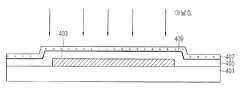
또 한편, 본 발명의 제3 실시 예에 따른 산화물 박막트랜지스터 구조에 대해 도 8을 참조하여 설명하면 다음과 같다.On the other hand, the oxide thin film transistor structure according to the third embodiment of the present invention will be described with reference to FIG.
도 8은 본 발명의 제3 실시 예에 따른 산화물 박막 트랜지스터의 개략적인 단면도이다.8 is a schematic cross-sectional view of an oxide thin film transistor according to a third exemplary embodiment of the present invention.
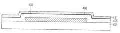
본 발명의 제3 실시 예에 따른 산화물 박막트랜지스터(400)는, 도 8에 도시된 바와 같이, 기판(401)상에 형성된 게이트전극(403)과; 상기 게이트전극(403)을 포함한 기판 전면에 형성된 게이트 절연막(405)과; 상기 게이트전극(403) 상측의 게이트 절연막(405) 상에 형성된 액티브패턴(411a)과; 상기 액티브패턴(411a)의 하부 표면에 형성된 합금 산화막패턴(alloy oxide)(409a)과; 상기 액티브패턴(411a)의 채널영역 상에 형성된 식각정지층패턴(415)과; 상기 액티브패턴(411a)과 게이트절연막(405) 상에 형성되고, 서로 이격된 소스전극(417a) 및 드레인전극 (417b)을 포함하여 구성된다.An oxide
여기서, 상기 합금 산화막패턴(409a)은 상기 게이트절연막(405)과 접촉하는 상기 액티브패턴(411a)의 하부 표면에 형성된다.Here, the alloy
상기 본 발명의 제3 실시 예에 따른 산화물 박막트랜지스터(400)는 탑 게이트(Top gate), 바텀 게이트(Bottom gate) 방식 등을 포함하여 구동 가능한 박막트랜지스터 구조를 모두 포함한다. 또한, 상기 박막트랜지스터(200)는 식각정지층을 사용하는 박막트랜지스터 및 BCE 구조의 박막트랜지스터를 포함한다.The oxide
본 발명에 따른 박막트랜지스터(400)는 액정표시장치 (Liquid Crystal Display; 이하 LCD라 함), 유기발광 다이오드(Organic Luminescence Emitted Diode; 이하 OLED라 함) 등 평판 디스플레이의 구동 소자 또는 스위칭 소자나, 메모리 소자의 주변 회로 구성을 위한 소자 등 다양한 전자 소자에 적용될 수 있다.The
상기 기판(401)은 실리콘, 유리, 플라스틱 또는 다른 적절한 물질을 포함하여 이루어질 수 있다.The
상기 게이트 전극(403)으로는, 알루미늄(Al), 알루미늄 합금(Al alloy), 텅스텐(W), 구리(Cu), 구리(Cu) 합금, 몰리브덴(Mo), 은(Ag), 은 합금(Ag alloy), 금(Au), 금 합금(Au alloy), 크롬(Cr), 티타늄(Ti), 티타늄 합금(Ti alloy), 몰리텅스텐(MoW), 몰리티타늄 (MoTi), 구리/몰리티타늄 (Cu/MoTi)을 포함하는 도전성 금속 그룹 중에서 선택된 적어도 어느 하나 또는 이들의 2 이상의 조합 또는 다른 적절한 물질을 포함할 수도 있다.As the
또한, 상기 게이트 절연막(405)으로는 실리콘(Si) 계열의 산화막, 질화막, 또는 이를 포함하는 화합물과, Al2O3를 포함하는 금속산화막(metal oxide), 유기절연막, 낮은 유전 상수(low-k) 값을 갖는 재료를 포함한다. 예를 들어, 상기 게이트절연막(107)으로는, 산화실리콘(SiO2), 질화실리콘(SiNx), 산화지르코늄(ZrO2), 산화하프늄(HfO2), 산화티타늄(TiO2), 산화탄탈륨(Ta2O5), 바륨-스트론튬-티타늄-산소화합물(Ba-Sr-Ti-O) 및 비스머스-아연-니오븀-산소 화합물(Bi-Zn-Nb-O)로 이루어지는 그룹으로부터 선택되는 어느 하나 또는 이들의 2 이상의 조합 또는 다른 적절한 물질을 포함할 수도 있다.In addition, the
그리고, 상기 액티브패턴(411a)은 소스전극(417a)과 드레인전극(417b) 사이에 전자가 이동하는 채널을 형성하기 위한 층으로서, 저온 다결정 실리콘(Low Temperature Poly Silicon; 이하 LTPS라 함) 또는 비정질 실리콘(a-Si) 재질 대신에 실리콘(Si) 계열의 반도체 막, IGZO 계열의 산화물 반도체막, 화합물 반도체, 카본 나노 튜브(Carbon nano tube), 그라핀(graphene)을 사용한다.The
이때, 상기 산화물 반도체로는, 게르마늄 (Ge), 주석(Sn), 납(Pb), 인듐 (In), 티타늄(Ti), 갈륨(Ga) 및 알루미늄(Al)으로 이루어지는 그룹으로부터 선택된 하나 이상의 물질 및 아연(Zn)을 포함하는 산화물 반도체에 실리콘(Si)이 첨가된 물질로 이루어질 수 있다. 예컨대, 상기 액티브패턴(109a)은 인듐아연 복합 산화물(InZnO)에 실리콘 이온이 첨가된 실리콘 산화인듐아연(Si-InZnO: SIZO)으로 이루어질 수도 있다.In this case, the oxide semiconductor, at least one material selected from the group consisting of germanium (Ge), tin (Sn), lead (Pb), indium (In), titanium (Ti), gallium (Ga) and aluminum (Al). And silicon (Si) added to the oxide semiconductor including zinc (Zn). For example, the active pattern 109a may be formed of silicon indium zinc oxide (Si-InZnO: SIZO) in which silicon ions are added to indium zinc complex oxide (InZnO).
상기 액티브패턴(411a)이 SIZO로 이루어지는 경우, 액티브층에서 아연(Zn), 인듐(In) 및 실리콘(Si) 원자의 전체 함량 대비 실리콘(Si) 원자 함량의 조성비는 약 0.001 중량%(wt%) 내지 약 30 wt%일 수도 있다. 실리콘(Si) 원자 함량이 높아질수록 전자 생성을 제어하는 역할이 강해져서, 이동도가 낮아질 수 있으나, 그 소자의 안정성은 더 좋아질 수 있다.When the
한편, 상기 액티브패턴(411a)으로는, 전술한 물질 외에 리튬(Li) 또는 칼륨(K)과 같은 I족 원소, 마그네슘(Mg), 칼슘(Ca) 또는 스트론튬(Sr)과 같은 Ⅱ족 원소, 갈륨(Ga), 알루미늄(Al), 인듐(In) 또는 이트륨(Y)과 같은 Ⅲ족 원소, 티타늄(Ti), 지르코늄(Zr), 실리콘(Si), 주석(Sn) 또는 게르마늄(Ge)과 같은 Ⅳ족 원소, 탄탈륨(Ta), 바나듐(V), 니오븀(Nb) 또는 안티몬(Sb)과 같은 Ⅴ족 원소, 또는 란티늄(La), 세륨(Ce), 프라세오디뮴(Pr), 네오디뮴(Nd), 프로메튬(Pm), 사마륨 (Sm), 유로퓸(Eu), 가돌리듐(Gd), 터븀(Tb), 디스프로슘(Dy), 홀뮴(Ho), 어븀(Er), 툴륨(Tm), 이터븀(Yb) 또는 루테듐(Lu)과 같은 란탄(Ln) 계열 원소 등이 더 포함될 수도 있다.On the other hand, as the
상기 합금 산화막패턴(409a)은 Cu 합금, Ag 합금, Au 합금, Al 합금을 포함하는 반응성 합금 또는 Ti, Zr, Hf, V, Nb, Ta, Cr, Mo, W, Mn, Fe, Co, Ni 및 이를 포함한 합금 막으로 구성된 금속 중에서 어느 하나를 이용하여 형성될 수 있다.The alloy
또한, 상기 식각정지층패턴(415)은 실리콘(Si) 계열의 산화막(oxide), 질화막(nitride), 또는 Al2O3를 포함하는 금속산화막(metal oxide), 유기절연막, 낮은 유전 상수(low-k) 값을 갖는 재료를 포함한다.In addition, the etch
더욱이, 상기 소스전극(417a) 및 드레인전극(417b)으로는 알루미늄(Al), 알루미늄 합금(Al alloy), 텅스텐(W), 구리(Cu), Cu 합금, 몰리브덴(Mo), 은(Ag), 은 합금(Ag alloy), 금(Au), 금 합금(Au alloy), 크롬(Cr), 티타늄(Ti), 티타늄 합금(Ti alloy), 몰리텅스텐(MoW), 몰리티타늄 (MoTi), 구리/몰리티타늄 (Cu/MoTi)을 포함하는 도전성 금속 그룹 중에서 선택된 적어도 어느 하나 또는 이들의 2 이상의 조합 또는 다른 적절한 물질을 포함할 수도 있다.Further, the
따라서, 본 발명의 제3 실시 예에 따른 산화물 박막트랜지스터에 따르면, 산화물 반도체를 액티브층으로 사용하는 박막트랜지스터 구조에서 산화물 반도체층을 증착한 이후에 다시 금속 합금층을 증착하고 이후 열처리를 통해 상기 산화물 반도체층 표면에 합금 산화막을 형성하고 잔류하는 금속 합금층은 식각하여, 자기 정렬 (Self-aligned) 방법으로 산화물 반도체층 표면에만 합금 산화막을 형성함으로써, 산화물 반도체층을 외부 환경으로부터 보호할 수 있으며, 안정적인 소자 특성을 확보할 수 있다.Therefore, according to the oxide thin film transistor according to the third embodiment of the present invention, in the thin film transistor structure using the oxide semiconductor as an active layer, after depositing the oxide semiconductor layer, the metal alloy layer is deposited again and then the oxide through heat treatment The alloy oxide film is formed on the surface of the semiconductor layer and the remaining metal alloy layer is etched to form the alloy oxide film only on the surface of the oxide semiconductor layer by a self-aligned method, thereby protecting the oxide semiconductor layer from the external environment. Stable device characteristics can be secured.
상기 구성으로 이루어지는 본 발명의 제3 실시 예에 따른 산화물 박막트랜지스터 제조방법에 대해 도 9a 내지 9h를 참조하여 상세히 설명한다.An oxide thin film transistor manufacturing method according to a third exemplary embodiment of the present invention having the above configuration will be described in detail with reference to FIGS. 9A to 9H.
도 9a 내지 9h는 본 발명의 제3 실시 예에 따른 산화물 박막 트랜지스터의 제조공정 단면도들이다.9A to 9H are cross-sectional views illustrating a process of manufacturing an oxide thin film transistor according to a third exemplary embodiment of the present invention.
도면에는 도시하지 않았지만, 기판(401)상에 게이트전극용 제1 도전물질을 스퍼터링방법으로 증착하여 제1 도전층(미도시)을 형성하고, 그 위에 제1 감광막(미도시)을 도포한 후, 포토리소그라피 공정기술을 이용한 제1 마스크 공정을 통해 상기 제1 감광막(미도시)을 패터닝하여 제1 감광막패턴(미도시)을 형성한다.Although not shown in the drawing, a first conductive material for a gate electrode is deposited on the
이때, 상기 기판(401)은 실리콘, 유리, 플라스틱 또는 다른 적절한 물질을 포함하여 이루어질 수 있다.In this case, the
또한, 상기 제1 도전층(미도시)으로는, 알루미늄(Al), 알루미늄 합금(Al alloy), 텅스텐(W), 구리(Cu), 구리(Cu) 합금, 몰리브덴(Mo), 은(Ag), 은 합금(Ag alloy), 금(Au), 금 합금(Au alloy), 크롬(Cr), 티타늄(Ti), 티타늄 합금(Ti alloy), 몰리텅스텐 (MoW), 몰리티타늄 (MoTi), 구리/몰리티타늄 (Cu/MoTi)을 포함하는 도전성 금속 그룹 중에서 선택된 적어도 어느 하나 또는 이들의 2 이상의 조합 또는 다른 적절한 물질을 포함할 수도 있다.In addition, as the first conductive layer (not shown), aluminum (Al), aluminum alloy (Al alloy), tungsten (W), copper (Cu), copper (Cu) alloy, molybdenum (Mo), silver (Ag) ), Silver alloy (Ag), gold (Au), gold alloy (Au alloy), chromium (Cr), titanium (Ti), titanium alloy (Ti alloy), molybdenum (MoW), molybdenum (MoTi), It may also comprise at least any one selected from the group of conductive metals comprising copper / mortitanium (Cu / MoTi) or a combination of two or more thereof or other suitable materials.
그 다음, 도 9a를 참조하면, 상기 제1 감광막패턴(미도시)을 식각 마스크로 상기 제1 도전층(미도시)을 선택적으로 식각하여 게이트전극(403)을 형성한다.Next, referring to FIG. 9A, the first conductive layer (not shown) is selectively etched using the first photoresist pattern (not shown) as an etching mask to form a
이어서, 도 9b를 참조하면, 상기 제1 감광막패턴을 제거하고, 상기 게이트전극(403)을 포함한 기판 전면에 게이트 절연막(405)을 형성한다. 이때, 상기 게이트 절연막(405)으로는 실리콘(Si) 계열의 산화막, 질화막, 또는 이를 포함하는 화합물과, Al2O3를 포함하는 금속산화막(metal oxide), 유기절연막, 낮은 유전 상수 (low-k) 값을 갖는 재료를 포함한다. 예를 들어, 상기 게이트절연막(305)으로는, 산화실리콘(SiO2), 질화실리콘(SiNx), 산화지르코늄(ZrO2), 산화하프늄(HfO2), 산화티타늄(TiO2), 산화탄탈륨(Ta2O5), 바륨-스트론튬-티타늄-산소화합물 (Ba-Sr-Ti-O) 및 비스머스-아연-니오븀-산소 화합물(Bi-Zn-Nb-O)로 이루어지는 그룹으로부터 선택되는 어느 하나 또는 이들의 2 이상의 조합 또는 다른 적절한 물질을 포함할 수도 있다.Subsequently, referring to FIG. 9B, the first photoresist layer pattern is removed, and a
그 다음, 도 9c를 참조하면, 상기 게이트절연막(405) 상에 반응성 금속층 (407)을 증착한다. 이때, 상기 반응성 금속층(407)은 Cu 합금, Ag 합금, Au 합금, Al 합금을 포함하는 반응성 합금 또는 Ti, Zr, Hf, V, Nb, Ta, Cr, Mo, W, Mn, Fe, Co, Ni 및 이를 포함한 합금 막으로 구성된 금속 중에서 어느 하나를 이용하여 형성될 수 있다. 이때, 상기 합금 원소는 Ca, Mg, Zn, Al, Zr, V, Nb, Ta, Cr, Mo, W, Mn, Fe, Ru, Co, Ni, Ag, Au, Zn 을 포함한다.Next, referring to FIG. 9C, a
이어서, 도 9d를 참조하면, 아닐링 공정을 실시하여, 상기 반응성 금속층 (407)과 접촉하는 상기 게이트절연막(405)의 표면에 합금산화막(alloy oxide) (409)을 형성한다. 이때, 상기 아닐링 공정은 상압, 진공 아닐링 (annealing) 방법을 모두 포함하며, 열원으로는 광원으로 이용하는 방법도 모두 포함할 수 있다. 이때, 상기 합금산화막(409)은 자기 정렬(Self-aligned) 방법으로 형성된다고 볼 수 있다.9D, an annealing process is performed to form an
그 다음, 상기 반응성 금속층(407)을 습식 식각 방법을 통해 제거하여, 상기 게이트절연막(405) 표면에 있는 합금산화막(409)을 외부로 노출시킨다.Next, the
이어서, 도 9e를 참조하면, 상기 합금산화막(409) 상에 액티브층(411)을 형성한다. 이때, 상기 액티브층(411)은 소스전극(미도시)과 드레인전극(미도시) 사이에 전자가 이동하는 채널을 형성하기 위한 층으로서, 저온 다결정 실리콘(Low Temperature Poly Silicon; 이하 LTPS라 함) 또는 비정질 실리콘(a-Si) 재질 대신에 실리콘(Si) 계열의 반도체 막, IGZO 계열의 산화물 반도체막, 화합물 반도체, 카본 나노 튜브 (Carbon nano tube), 그라핀(graphene)을 사용한다.Next, referring to FIG. 9E, an
이때, 상기 산화물 반도체로는, 게르마늄 (Ge), 주석(Sn), 납(Pb), 인듐 (In), 티타늄(Ti), 갈륨(Ga) 및 알루미늄(Al)으로 이루어지는 그룹으로부터 선택된 하나 이상의 물질 및 아연(Zn)을 포함하는 산화물 반도체에 실리콘(Si)이 첨가된 물질로 이루어질 수 있다. 예컨대, 상기 액티브층(109)은 인듐아연 복합 산화물 (InZnO)에 실리콘 이온이 첨가된 실리콘 산화인듐아연(Si-InZnO: SIZO)으로 이루어질 수도 있다.In this case, the oxide semiconductor, at least one material selected from the group consisting of germanium (Ge), tin (Sn), lead (Pb), indium (In), titanium (Ti), gallium (Ga) and aluminum (Al). And silicon (Si) added to the oxide semiconductor including zinc (Zn). For example, the
상기 액티브층(411)이 SIZO로 이루어지는 경우, 액티브층에서 아연(Zn), 인듐(In) 및 실리콘(Si) 원자의 전체 함량 대비 실리콘(Si) 원자 함량의 조성비는 약 0.001 중량%(wt%) 내지 약 30 wt%일 수도 있다. 실리콘(Si) 원자 함량이 높아질수록 전자 생성을 제어하는 역할이 강해져서, 이동도가 낮아질 수 있으나, 그 소자의 안정성은 더 좋아질 수 있다.When the
한편, 상기 액티브층(411)으로는, 전술한 물질 외에 리튬(Li) 또는 칼륨(K)과 같은 I족 원소, 마그네슘(Mg), 칼슘(Ca) 또는 스트론튬(Sr)과 같은 Ⅱ족 원소, 갈륨(Ga), 알루미늄(Al), 인듐(In) 또는 이트륨(Y)과 같은 Ⅲ족 원소, 티타늄(Ti), 지르코늄(Zr), 실리콘(Si), 주석(Sn) 또는 게르마늄(Ge)과 같은 Ⅳ족 원소, 탄탈륨 (Ta), 바나듐(V), 니오븀(Nb) 또는 안티몬(Sb)과 같은 Ⅴ족 원소, 또는 란티늄 (La), 세륨(Ce), 프라세오디뮴(Pr), 네오디뮴(Nd), 프로메튬(Pm), 사마륨 (Sm), 유로퓸(Eu), 가돌리듐(Gd), 터븀(Tb), 디스프로슘(Dy), 홀뮴(Ho), 어븀(Er), 툴륨 (Tm), 이터븀(Yb) 또는 루테듐(Lu)과 같은 란탄(Ln) 계열 원소 등이 더 포함될 수도 있다.On the other hand, as the
이어서, 도면에는 도시하지 않았지만, 상기 액티브층(411) 상에 제2 감광막(미도시)을 도포한 후, 포토리소그라피 공정기술을 이용한 제2 마스크 공정을 통해 상기 제2 감광막(미도시)을 노광 및 현상한 후 상기 제2 감광막(미도시)을 선택적으로 패터닝하여 제2 감광막패턴(미도시)을 형성한다.Subsequently, although not shown in the drawings, a second photosensitive film (not shown) is coated on the
그 다음, 도 9f를 참조하면, 상기 제2 감광막패턴(미도시)을 식각마스크로, 상기 액티브층(411) 및 합금 산화막(409)을 선택적으로 식각하여 액티브패턴(411a) 및 합금 산화막패턴(409a)을 형성한다.Next, referring to FIG. 9F, the
이어서, 도면에는 도시하지 않았지만, 상기 제2 감광막패턴을 제거한 후, 기판 전면에 식각정지층(미도시)을 증착한다. 이때, 상기 식각정지층(미도시)은 실리콘(Si) 계열의 산화막(oxide), 질화막(nitride), 또는 Al2O3를 포함하는 금속산화막 (metal oxide), 유기절연막, 낮은 유전 상수(low-k) 값을 갖는 재료를 포함한다.Subsequently, although not shown, after removing the second photoresist pattern, an etch stop layer (not shown) is deposited on the entire surface of the substrate. In this case, the etch stop layer (not shown) is a silicon oxide (oxide), nitride (nitride), or a metal oxide film (metal oxide), including an Al2 O3 (organic insulating film, low dielectric constant (low) -k) include materials with values.
그 다음, 상기 식각정지층 상에 제3 감광막(미도시)을 도포한 후, 포토리소그라피 공정기술을 이용한 제3 마스크 공정을 통해 상기 제2 감광막(미도시)을 노광 및 현상한 후 상기 제3 감광막(미도시)을 선택적으로 패터닝하여 제3 감광막패턴(미도시)을 형성한다.Thereafter, after applying a third photoresist film (not shown) on the etch stop layer, the third photoresist film (not shown) is exposed and developed through a third mask process using a photolithography process technology, and then the third photoresist film is exposed. A photoresist layer (not shown) is selectively patterned to form a third photoresist layer pattern (not shown).
이어서, 도 9g를 참조하면, 상기 제3 감광막패턴을 식각 마스크로, 상기 식각정지층을 선택적으로 제거하여, 상기 액티브패턴(411a)의 채널영역 상에 식각정지층패턴(415)을 형성한다.Subsequently, referring to FIG. 9G, the etch stop layer is selectively removed by using the third photoresist pattern as an etch mask to form an etch
그 다음, 상기 제3 감광막패턴을 제거한 후, 상기 식각정지층(415)을 포함한 기판 전면에 제2 도전층(미도시)을 스퍼터링 방법으로 증착하여 형성한다. 이때, 상기 제2 도전층(미도시)으로는, 알루미늄(Al), 알루미늄 합금(Al alloy), 텅스텐(W), 구리(Cu), Cu 합금, 몰리브덴(Mo), 은(Ag), 은 합금(Ag alloy), 금(Au), 금 합금(Au alloy), 크롬(Cr), 티타늄(Ti), 티타늄 합금(Ti alloy), 몰리텅스텐 (MoW), 몰리티타늄 (MoTi), 구리/몰리티타늄 (Cu/MoTi)을 포함하는 도전성 금속 그룹 중에서 선택된 적어도 어느 하나 또는 이들의 2 이상의 조합 또는 다른 적절한 물질을 포함할 수도 있다.After removing the third photoresist pattern, a second conductive layer (not shown) is formed on the entire surface of the substrate including the
이어서, 상기 제2 도전층(미도시) 상에 제4 감광막(미도시)을 도포한 후 포토리소그라피 공정기술을 이용한 제4 마스크 공정을 통해 상기 제4 감광막(미도시)을 노광 및 현상한 후 상기 제4 감광막(미도시)을 선택적으로 패터닝하여 제4 감광막패턴(미도시)을 형성한다.Subsequently, after applying a fourth photoresist film (not shown) on the second conductive layer (not shown) and exposing and developing the fourth photoresist film (not shown) through a fourth mask process using a photolithography process technology. The fourth photoresist layer (not shown) is selectively patterned to form a fourth photoresist layer pattern (not shown).
그 다음, 도 9h를 참조하면, 상기 제4 감광막패턴(미도시)을 식각마스크로, 상기 제2 도전층(미도시)을 식각하여, 상기 이격된 소스전극(417a) 및 드레인전극 (417b)을 형성하고 제4 감광막패턴(미도시)을 제거함으로써, 본 발명의 제3 실시 예에 따른 산화물 박막트랜지스터 제조공정을 완료한다.Next, referring to FIG. 9H, the fourth photoresist layer pattern (not shown) is etched and the second conductive layer (not shown) is etched to separate the
따라서, 본 발명에 따른 산화물 박막트랜지스터 제조방법에 따르면, 산화물 반도체를 액티브층으로 사용하는 박막트랜지스터 구조에서 산화물 반도체층을 증착한 이후에 다시 금속 합금층을 증착하고 이후 열처리를 통해 상기 산화물 반도체층 표면에 합금 산화막을 형성하고 잔류하는 금속 합금층은 식각하여, 자기 정렬 (Self-aligned) 방법으로 산화물 반도체층 표면에만 합금 산화막을 형성함으로써, 산화물 반도체층을 외부 환경으로부터 보호할 수 있으며, 안정적인 소자 특성을 확보할 수 있다.Accordingly, according to the method of manufacturing an oxide thin film transistor according to the present invention, in the thin film transistor structure using the oxide semiconductor as an active layer, the metal alloy layer is deposited again after the oxide semiconductor layer is deposited, and then the surface of the oxide semiconductor layer through heat treatment. The alloy oxide film is formed on the metal oxide layer, and the remaining metal alloy layer is etched to form the alloy oxide film only on the surface of the oxide semiconductor layer by a self-aligned method, thereby protecting the oxide semiconductor layer from the external environment. Can be secured.
상기한 설명에서 많은 사항이 구체적으로 기재되어 있으나, 그들은 발명의 범위를 한정하는 것이라기보다, 바람직한 실시 예의 예시로서 해석되어야 한다. 예를 들어, 본 발명이 속하는 기술 분야에서 통상의 지식을 가진 자라면, 본 발명의 박막트랜지스터의 구성 요소는 다양화할 수 있을 것이고, 구조 또한 다양한 형태로 변형할 수 있을 것이다.While many details are set forth in the foregoing description, they should be construed as illustrative of preferred embodiments, rather than to limit the scope of the invention. For example, those of ordinary skill in the art to which the present invention pertains will be able to vary the components of the thin film transistor of the present invention, the structure may also be modified in various forms.
본 발명의 산화물 박막 트랜지스터는 액정표시장치나 유기발광표시장치뿐만 아니라 메모리소자 및 논리 소자 분야에도 적용될 수 있음을 알 수 있을 것이다. 때문에 본 발명의 범위는 설명된 실시 예에 의하여 정하여 질 것이 아니고 특허 청구범위에 기재된 기술적 사상에 의해 정하여져야 한다.It will be appreciated that the oxide thin film transistor of the present invention can be applied not only to liquid crystal display devices and organic light emitting display devices but also to memory devices and logic devices. Therefore, the scope of the present invention should not be defined by the described embodiments, but should be determined by the technical spirit described in the claims.
100: 산화물 박막트랜지스터103: 게이트전극
105: 게이트 절연막107: 액티브패턴
111: 합금 산화막113a: 소스전극113b: 드레인전극100: oxide thin film transistor 103: the gate electrode
105: gate insulating film 107: active pattern
111:
Claims (15)
Translated fromKorean상기 게이트전극을 포함한 기판 전면에 형성된 게이트 절연막과;
상기 게이트전극 상측의 게이트 절연막 상의 일부분에 형성된 산화물 반도체막으로 이루어진 액티브패턴과;
상기 액티브패턴의 측면 및 상면 전체에 직접 접촉되어 위치하는 합금 산화막과;
상기 합금 산화막과 상기 게이트절연막상에 형성되고, 서로 이격된 소스전극 및 드레인 전극;을 포함하며, 상기 소스전극 및 드레인전극의 상기 액티브패턴과 중첩하지 않는 부분은 상기 게이트 절연막과 접하는, 박막트랜지스터.A gate electrode formed on the substrate;
A gate insulating film formed on an entire surface of the substrate including the gate electrode;
An active pattern made of an oxide semiconductor film formed on a portion of the gate insulating film above the gate electrode;
An alloy oxide layer in direct contact with the entire side and top surfaces of the active pattern;
And a source electrode and a drain electrode formed on the alloy oxide film and the gate insulating film and spaced apart from each other, wherein portions of the source electrode and the drain electrode that do not overlap the active pattern are in contact with the gate insulating film.
상기 게이트전극을 포함한 기판 전면에 형성된 게이트 절연막과;
상기 게이트전극 상측의 게이트 절연막 상의 일부분에 형성된 산화물 반도체막으로 이루어진 액티브패턴과;
상기 액티브패턴의 하면, 측면 및 상면 전체에 직접 접촉되어 위치하는 합금 산화막과;
상기 합금 산화막과 상기 게이트절연막상에 형성되고, 서로 이격된 소스전극 및 드레인 전극;을 포함하며, 상기 소스전극 및 드레인전극의 상기 액티브패턴과 중첩하지 않는 부분은 상기 게이트 절연막과 접하는, 박막트랜지스터.A gate electrode formed on the substrate;
A gate insulating film formed on an entire surface of the substrate including the gate electrode;
An active pattern made of an oxide semiconductor film formed on a portion of the gate insulating film above the gate electrode;
An alloy oxide film positioned in direct contact with the entire lower surface, the side surface, and the upper surface of the active pattern;
And a source electrode and a drain electrode formed on the alloy oxide film and the gate insulating film and spaced apart from each other, wherein portions of the source electrode and the drain electrode that do not overlap the active pattern are in contact with the gate insulating film.
상기 게이트전극을 포함한 기판 전면에 게이트 절연막을 형성하는 단계와;
상기 게이트전극 상측의 게이트 절연막 상의 일부분에 산화물 반도체막으로 이루어진 액티브패턴을 형성하는 단계와;
상기 액티브패턴의 측면 및 상면 전체에 직접 접촉되게 합금 산화막을 형성하는 단계와;
상기 합금 산화막과 게이트절연막 상에 서로 이격된 소스전극과 드레인전극을 형성하는 단계;를 포함하며, 상기 소스전극 및 드레인전극의 상기 액티브패턴과 중첩하지 않는 부분은 상기 게이트 절연막과 접하는, 박막트랜지스터 제조방법.Forming a gate electrode on the substrate;
Forming a gate insulating film on an entire surface of the substrate including the gate electrode;
Forming an active pattern made of an oxide semiconductor film on a portion of the gate insulating film above the gate electrode;
Forming an alloy oxide film in direct contact with the entire side and top surfaces of the active pattern;
Forming a source electrode and a drain electrode spaced apart from each other on the alloy oxide film and the gate insulating film, wherein a portion of the source electrode and the drain electrode not overlapping with the active pattern is in contact with the gate insulating film. Way.
상기 게이트 절연막 및 상기 액티브패턴 상에 반응성 금속층을 형성하는 공정과;
아닐링 공정을 실시하여 상기 반응성 금속층과 접촉하는 상기 액티브패턴 측면 및 상면 전체에 합금 산화막을 형성하는 공정과;
상기 반응성 금속층을 제거하는 공정을 포함하여 구성되는 것을 특징으로 하는 박막트랜지스터 제조방법.The method of claim 6, wherein the step of forming an alloy oxide film in direct contact with the entire side and top of the active pattern,
Forming a reactive metal layer on the gate insulating layer and the active pattern;
Performing an annealing process to form an alloy oxide film on the entire side and top surfaces of the active pattern in contact with the reactive metal layer;
Thin film transistor manufacturing method comprising the step of removing the reactive metal layer.
상기 게이트 절연막을 형성한 후에 상기 게이트절연막 상에 제1 반응성 금속층을 형성하는 공정과;
1차 아닐링 공정을 실시하여 상기 제1 반응성 금속층과 접촉하는 상기 게이트절연막 표면에 제1 합금 산화막을 형성하는 공정과;
상기 제1 반응성 금속층을 제거하여 상기 제1 합금 산화막을 외부로 노출시키는 공정;을 포함하고, 상기 액티브패턴을 형성하는 단계는,
상기 제1 합금 산화막 상에 액티브층을 형성하는 공정과;
상기 액티브층과 제1 합금 산화막을 선택적으로 식각하여, 게이트 절연막 상의 일부분에 액티브패턴과 상기 액티브패턴 하부의 제1 합금 산화막패턴을 형성하는 공정;을 포함하고, 상기 합금 산화막을 형성하는 단계는,
상기 액티브패턴과 상기 게이트 절연막 상에 제2 반응성 금속층을 형성하는 공정과;
2차 아닐링 공정을 실시하여 상기 제2 반응성 금속층과 접촉하는 상기 액티브패턴의 측면 및 상면 전체에 직접 접촉되게 제2 합금 산화막을 형성하는 공정과;
상기 제2 반응성 금속층을 제거하는 공정을 포함하여 구성되는 것을 특징으로 하는 박막트랜지스터 제조방법.The method of claim 7, wherein the forming of the first alloy oxide film,
Forming a first reactive metal layer on the gate insulating film after forming the gate insulating film;
Performing a first annealing process to form a first alloy oxide film on a surface of the gate insulating film in contact with the first reactive metal layer;
Removing the first reactive metal layer to expose the first alloy oxide layer to the outside; and forming the active pattern includes:
Forming an active layer on the first alloy oxide film;
And selectively etching the active layer and the first alloy oxide layer to form an active pattern and a first alloy oxide pattern under the active pattern on a portion of the gate insulating layer, wherein the forming of the alloy oxide layer comprises:
Forming a second reactive metal layer on the active pattern and the gate insulating film;
Performing a second annealing process to form a second alloy oxide film in direct contact with the entire side and top surfaces of the active pattern in contact with the second reactive metal layer;
Thin film transistor manufacturing method comprising the step of removing the second reactive metal layer.
상기 액티브패턴 및 게이트절연막 상에 반응성 금속층을 형성하는 공정과;
아닐링 공정을 실시하여 상기 반응성 금속층과 접촉하는 상기 액티브패턴 측면및 상부 표면에 합금 산화막을 형성하는 공정과;
상기 반응성 금속층 상에 감광막패턴을 형성하는 공정과;
상기 감광막패턴을 식각마스크로 상기 반응성 금속층을 식각하여 소스전극 및 드레인 전극을 형성하는 공정을 포함하여 구성되는 것을 특징으로 하는 박막트랜지스터 제조방법.The method of claim 6, wherein the forming of the alloy oxide layer and the forming of the source electrode and the drain electrode include:
Forming a reactive metal layer on the active pattern and the gate insulating film;
Performing an annealing process to form an alloy oxide film on the side surfaces and top surfaces of the active pattern in contact with the reactive metal layer;
Forming a photoresist pattern on the reactive metal layer;
And forming a source electrode and a drain electrode by etching the reactive metal layer using the photoresist pattern as an etching mask.
Priority Applications (1)
| Application Number | Priority Date | Filing Date | Title |
|---|---|---|---|
| KR1020120109501AKR102009017B1 (en) | 2012-09-28 | 2012-09-28 | Oxide thin film transistor for display device and method for fabricating the same |
Applications Claiming Priority (1)
| Application Number | Priority Date | Filing Date | Title |
|---|---|---|---|
| KR1020120109501AKR102009017B1 (en) | 2012-09-28 | 2012-09-28 | Oxide thin film transistor for display device and method for fabricating the same |
Publications (2)
| Publication Number | Publication Date |
|---|---|
| KR20140042572A KR20140042572A (en) | 2014-04-07 |
| KR102009017B1true KR102009017B1 (en) | 2019-10-23 |
Family
ID=50651716
Family Applications (1)
| Application Number | Title | Priority Date | Filing Date |
|---|---|---|---|
| KR1020120109501AActiveKR102009017B1 (en) | 2012-09-28 | 2012-09-28 | Oxide thin film transistor for display device and method for fabricating the same |
Country Status (1)
| Country | Link |
|---|---|
| KR (1) | KR102009017B1 (en) |
Citations (1)
| Publication number | Priority date | Publication date | Assignee | Title |
|---|---|---|---|---|
| JP2008124499A (en)* | 2005-02-17 | 2008-05-29 | Kobe Steel Ltd | Thin-film transistor substrate, display device, and sputtering target for display device |
Family Cites Families (3)
| Publication number | Priority date | Publication date | Assignee | Title |
|---|---|---|---|---|
| KR100963027B1 (en)* | 2008-06-30 | 2010-06-10 | 삼성모바일디스플레이주식회사 | Thin film transistor, its manufacturing method, and flat panel display device comprising thin film transistor |
| JP5584960B2 (en)* | 2008-07-03 | 2014-09-10 | ソニー株式会社 | Thin film transistor and display device |
| JP5708910B2 (en)* | 2010-03-30 | 2015-04-30 | ソニー株式会社 | THIN FILM TRANSISTOR, MANUFACTURING METHOD THEREOF, AND DISPLAY DEVICE |
- 2012
- 2012-09-28KRKR1020120109501Apatent/KR102009017B1/enactiveActive
Patent Citations (1)
| Publication number | Priority date | Publication date | Assignee | Title |
|---|---|---|---|---|
| JP2008124499A (en)* | 2005-02-17 | 2008-05-29 | Kobe Steel Ltd | Thin-film transistor substrate, display device, and sputtering target for display device |
Also Published As
| Publication number | Publication date |
|---|---|
| KR20140042572A (en) | 2014-04-07 |
Similar Documents
| Publication | Publication Date | Title |
|---|---|---|
| CN103427023B (en) | The method of oxide thin film transistor, its manufacture, there is the manufacture method of its display device and this display device | |
| KR102148478B1 (en) | Thin film transistor array substrate using oxide semiconductor and method for fabricating the same | |
| KR102023924B1 (en) | Oxide thin film transistor having array substrate for display device and method for fabricating the same | |
| KR102068089B1 (en) | Oxide semiconductor thin film transistor, method for fabricating tft, array substrate for display device having tft and method for fabricating the same | |
| JP6398000B2 (en) | Thin film transistor array substrate | |
| CN103077961B (en) | Amorphous oxide semiconductor and the thin-film transistor using it | |
| JP5279939B2 (en) | Semiconductor device | |
| US20100123136A1 (en) | Semiconductor device and manufacturing method thereof | |
| US8207530B2 (en) | Oxide semiconductor and thin film transistor including the same | |
| WO2015058581A1 (en) | Thin film transistor and preparation method therefor, array substrate and display | |
| KR20100132308A (en) | Thin Film Transistor and Manufacturing Method Thereof | |
| US9196746B2 (en) | Thin film transistor comprising main active layer and sub active layer, and method of manufacturing the same | |
| KR102070762B1 (en) | Oxide thin film transistor, method for fabricating tft, array substrate for display device having tft and method for fabricating the same | |
| JP2010205923A (en) | Method of manufacturing field effect transistor | |
| KR102142483B1 (en) | Method for fabricating thin film transistor array substrate for display device and the thin film transistor array substrate | |
| KR101375846B1 (en) | Thin film transistor and mehtod for fabricating the same | |
| JP2010205932A (en) | Field effect transistor | |
| KR102167136B1 (en) | Display device having thin film transistor array substrate and method for fabricating the same | |
| KR102135932B1 (en) | Thin film transistor array substrate for display device and method for fabricating the same | |
| KR101985399B1 (en) | Oxide thin film transistor for display device and method for fabricating the same | |
| KR102009017B1 (en) | Oxide thin film transistor for display device and method for fabricating the same | |
| CN106952823A (en) | Method for manufacturing metal oxide semiconductor thin film transistor | |
| KR20140042575A (en) | Oxide thin film transistor, method for fabricating tft, array substrate having tft and method for fabricating the same | |
| KR101987041B1 (en) | Method for fabricating oxide thin film transistor for display device | |
| US20250113542A1 (en) | Semiconductor device |
Legal Events
| Date | Code | Title | Description |
|---|---|---|---|
| PA0109 | Patent application | St.27 status event code:A-0-1-A10-A12-nap-PA0109 | |
| PG1501 | Laying open of application | St.27 status event code:A-1-1-Q10-Q12-nap-PG1501 | |
| R17-X000 | Change to representative recorded | St.27 status event code:A-3-3-R10-R17-oth-X000 | |
| A201 | Request for examination | ||
| PA0201 | Request for examination | St.27 status event code:A-1-2-D10-D11-exm-PA0201 | |
| D13-X000 | Search requested | St.27 status event code:A-1-2-D10-D13-srh-X000 | |
| D14-X000 | Search report completed | St.27 status event code:A-1-2-D10-D14-srh-X000 | |
| E902 | Notification of reason for refusal | ||
| PE0902 | Notice of grounds for rejection | St.27 status event code:A-1-2-D10-D21-exm-PE0902 | |
| AMND | Amendment | ||
| E13-X000 | Pre-grant limitation requested | St.27 status event code:A-2-3-E10-E13-lim-X000 | |
| P11-X000 | Amendment of application requested | St.27 status event code:A-2-2-P10-P11-nap-X000 | |
| P13-X000 | Application amended | St.27 status event code:A-2-2-P10-P13-nap-X000 | |
| E601 | Decision to refuse application | ||
| PE0601 | Decision on rejection of patent | St.27 status event code:N-2-6-B10-B15-exm-PE0601 | |
| AMND | Amendment | ||
| P11-X000 | Amendment of application requested | St.27 status event code:A-2-2-P10-P11-nap-X000 | |
| P13-X000 | Application amended | St.27 status event code:A-2-2-P10-P13-nap-X000 | |
| PX0901 | Re-examination | St.27 status event code:A-2-3-E10-E12-rex-PX0901 | |
| PX0701 | Decision of registration after re-examination | St.27 status event code:A-3-4-F10-F13-rex-PX0701 | |
| X701 | Decision to grant (after re-examination) | ||
| PR0701 | Registration of establishment | St.27 status event code:A-2-4-F10-F11-exm-PR0701 | |
| PR1002 | Payment of registration fee | St.27 status event code:A-2-2-U10-U11-oth-PR1002 Fee payment year number:1 | |
| PG1601 | Publication of registration | St.27 status event code:A-4-4-Q10-Q13-nap-PG1601 | |
| PR1001 | Payment of annual fee | St.27 status event code:A-4-4-U10-U11-oth-PR1001 Fee payment year number:4 | |
| PR1001 | Payment of annual fee | St.27 status event code:A-4-4-U10-U11-oth-PR1001 Fee payment year number:5 | |
| PR1001 | Payment of annual fee | St.27 status event code:A-4-4-U10-U11-oth-PR1001 Fee payment year number:6 | |
| P22-X000 | Classification modified | St.27 status event code:A-4-4-P10-P22-nap-X000 | |
| PR1001 | Payment of annual fee | St.27 status event code:A-4-4-U10-U11-oth-PR1001 Fee payment year number:7 |