KR102006389B1 - Light emitting device package and light emitting apparatus - Google Patents
Light emitting device package and light emitting apparatusDownload PDFInfo
- Publication number
- KR102006389B1 KR102006389B1KR1020130027491AKR20130027491AKR102006389B1KR 102006389 B1KR102006389 B1KR 102006389B1KR 1020130027491 AKR1020130027491 AKR 1020130027491AKR 20130027491 AKR20130027491 AKR 20130027491AKR 102006389 B1KR102006389 B1KR 102006389B1
- Authority
- KR
- South Korea
- Prior art keywords
- light emitting
- diode
- emitting device
- rectifying circuit
- conductive
- Prior art date
- Legal status (The legal status is an assumption and is not a legal conclusion. Google has not performed a legal analysis and makes no representation as to the accuracy of the status listed.)
- Active
Links
Images


Classifications
- H—ELECTRICITY
- H10—SEMICONDUCTOR DEVICES; ELECTRIC SOLID-STATE DEVICES NOT OTHERWISE PROVIDED FOR
- H10H—INORGANIC LIGHT-EMITTING SEMICONDUCTOR DEVICES HAVING POTENTIAL BARRIERS
- H10H20/00—Individual inorganic light-emitting semiconductor devices having potential barriers, e.g. light-emitting diodes [LED]
- H10H20/80—Constructional details
- H10H20/85—Packages
- H10H20/857—Interconnections, e.g. lead-frames, bond wires or solder balls
- H—ELECTRICITY
- H01—ELECTRIC ELEMENTS
- H01L—SEMICONDUCTOR DEVICES NOT COVERED BY CLASS H10
- H01L25/00—Assemblies consisting of a plurality of semiconductor or other solid state devices
- H01L25/16—Assemblies consisting of a plurality of semiconductor or other solid state devices the devices being of types provided for in two or more different subclasses of H10B, H10D, H10F, H10H, H10K or H10N, e.g. forming hybrid circuits
- H01L25/167—Assemblies consisting of a plurality of semiconductor or other solid state devices the devices being of types provided for in two or more different subclasses of H10B, H10D, H10F, H10H, H10K or H10N, e.g. forming hybrid circuits comprising optoelectronic devices, e.g. LED, photodiodes
- H—ELECTRICITY
- H01—ELECTRIC ELEMENTS
- H01L—SEMICONDUCTOR DEVICES NOT COVERED BY CLASS H10
- H01L24/00—Arrangements for connecting or disconnecting semiconductor or solid-state bodies; Methods or apparatus related thereto
- H01L24/73—Means for bonding being of different types provided for in two or more of groups H01L24/10, H01L24/18, H01L24/26, H01L24/34, H01L24/42, H01L24/50, H01L24/63, H01L24/71
- H—ELECTRICITY
- H05—ELECTRIC TECHNIQUES NOT OTHERWISE PROVIDED FOR
- H05B—ELECTRIC HEATING; ELECTRIC LIGHT SOURCES NOT OTHERWISE PROVIDED FOR; CIRCUIT ARRANGEMENTS FOR ELECTRIC LIGHT SOURCES, IN GENERAL
- H05B45/00—Circuit arrangements for operating light-emitting diodes [LED]
- H05B45/30—Driver circuits
- H—ELECTRICITY
- H10—SEMICONDUCTOR DEVICES; ELECTRIC SOLID-STATE DEVICES NOT OTHERWISE PROVIDED FOR
- H10H—INORGANIC LIGHT-EMITTING SEMICONDUCTOR DEVICES HAVING POTENTIAL BARRIERS
- H10H20/00—Individual inorganic light-emitting semiconductor devices having potential barriers, e.g. light-emitting diodes [LED]
- H10H20/80—Constructional details
- H10H20/85—Packages
- H—ELECTRICITY
- H01—ELECTRIC ELEMENTS
- H01L—SEMICONDUCTOR DEVICES NOT COVERED BY CLASS H10
- H01L2224/00—Indexing scheme for arrangements for connecting or disconnecting semiconductor or solid-state bodies and methods related thereto as covered by H01L24/00
- H01L2224/01—Means for bonding being attached to, or being formed on, the surface to be connected, e.g. chip-to-package, die-attach, "first-level" interconnects; Manufacturing methods related thereto
- H01L2224/42—Wire connectors; Manufacturing methods related thereto
- H01L2224/44—Structure, shape, material or disposition of the wire connectors prior to the connecting process
- H01L2224/45—Structure, shape, material or disposition of the wire connectors prior to the connecting process of an individual wire connector
- H01L2224/45001—Core members of the connector
- H01L2224/45099—Material
- H01L2224/451—Material with a principal constituent of the material being a metal or a metalloid, e.g. boron (B), silicon (Si), germanium (Ge), arsenic (As), antimony (Sb), tellurium (Te) and polonium (Po), and alloys thereof
- H01L2224/45138—Material with a principal constituent of the material being a metal or a metalloid, e.g. boron (B), silicon (Si), germanium (Ge), arsenic (As), antimony (Sb), tellurium (Te) and polonium (Po), and alloys thereof the principal constituent melting at a temperature of greater than or equal to 950°C and less than 1550°C
- H01L2224/45139—Silver (Ag) as principal constituent
- H—ELECTRICITY
- H01—ELECTRIC ELEMENTS
- H01L—SEMICONDUCTOR DEVICES NOT COVERED BY CLASS H10
- H01L2224/00—Indexing scheme for arrangements for connecting or disconnecting semiconductor or solid-state bodies and methods related thereto as covered by H01L24/00
- H01L2224/01—Means for bonding being attached to, or being formed on, the surface to be connected, e.g. chip-to-package, die-attach, "first-level" interconnects; Manufacturing methods related thereto
- H01L2224/42—Wire connectors; Manufacturing methods related thereto
- H01L2224/47—Structure, shape, material or disposition of the wire connectors after the connecting process
- H01L2224/48—Structure, shape, material or disposition of the wire connectors after the connecting process of an individual wire connector
- H01L2224/4805—Shape
- H01L2224/4809—Loop shape
- H01L2224/48091—Arched
- H—ELECTRICITY
- H01—ELECTRIC ELEMENTS
- H01L—SEMICONDUCTOR DEVICES NOT COVERED BY CLASS H10
- H01L2224/00—Indexing scheme for arrangements for connecting or disconnecting semiconductor or solid-state bodies and methods related thereto as covered by H01L24/00
- H01L2224/73—Means for bonding being of different types provided for in two or more of groups H01L2224/10, H01L2224/18, H01L2224/26, H01L2224/34, H01L2224/42, H01L2224/50, H01L2224/63, H01L2224/71
- H01L2224/732—Location after the connecting process
- H01L2224/73251—Location after the connecting process on different surfaces
- H01L2224/73257—Bump and wire connectors
- H—ELECTRICITY
- H01—ELECTRIC ELEMENTS
- H01L—SEMICONDUCTOR DEVICES NOT COVERED BY CLASS H10
- H01L2924/00—Indexing scheme for arrangements or methods for connecting or disconnecting semiconductor or solid-state bodies as covered by H01L24/00
- H01L2924/0001—Technical content checked by a classifier
- H01L2924/00014—Technical content checked by a classifier the subject-matter covered by the group, the symbol of which is combined with the symbol of this group, being disclosed without further technical details
- H—ELECTRICITY
- H01—ELECTRIC ELEMENTS
- H01L—SEMICONDUCTOR DEVICES NOT COVERED BY CLASS H10
- H01L2924/00—Indexing scheme for arrangements or methods for connecting or disconnecting semiconductor or solid-state bodies as covered by H01L24/00
- H01L2924/10—Details of semiconductor or other solid state devices to be connected
- H01L2924/11—Device type
- H01L2924/12—Passive devices, e.g. 2 terminal devices
- H01L2924/1203—Rectifying Diode
- H01L2924/12036—PN diode
- H—ELECTRICITY
- H01—ELECTRIC ELEMENTS
- H01L—SEMICONDUCTOR DEVICES NOT COVERED BY CLASS H10
- H01L2924/00—Indexing scheme for arrangements or methods for connecting or disconnecting semiconductor or solid-state bodies as covered by H01L24/00
- H01L2924/15—Details of package parts other than the semiconductor or other solid state devices to be connected
- H01L2924/151—Die mounting substrate
- H01L2924/156—Material
- H01L2924/15786—Material with a principal constituent of the material being a non metallic, non metalloid inorganic material
- H01L2924/15787—Ceramics, e.g. crystalline carbides, nitrides or oxides
Landscapes
- Engineering & Computer Science (AREA)
- Microelectronics & Electronic Packaging (AREA)
- Computer Hardware Design (AREA)
- Power Engineering (AREA)
- Physics & Mathematics (AREA)
- Condensed Matter Physics & Semiconductors (AREA)
- General Physics & Mathematics (AREA)
- Led Device Packages (AREA)
Abstract
Translated fromKoreanDescription
Translated fromKorean본 발명의 기술적 사상은 발광 소자 패키지 및 발광 장치에 관한 것으로, 교류 전원에서 직접 사용 가능한 발광 소자 패키지 및 발광 장치에 관한 것이다.Technical aspects of the present invention relate to a light emitting device package and a light emitting device, and a light emitting device package and a light emitting device that can be directly used in an AC power source.
발광 다이오드 (light emitting diode: LED)는 화합물 반도체 (compound semiconductor)의 PN 접합을 통해 전기적인 신호를 빛으로 변화시키는 발광 소자이다. LED는 그 자체로는 외부의 물리적, 화학적 충격에 의해 손상될 수 있기 때문에, 패키지 형태로 구현되어 실내외 조명, 자동차 헤드라이트, 디스플레이 장치의 백라이트 유닛 (back-light unit: BLU), 의료 기기 등 다양한 분야에 사용된다. 일반적으로 LED는 직류 전류로 구동되기 때문에, 상용 교류 전원에서 LED를 구동하기 위해서는 예컨대 정류 회로와 같은 추가적인 회로들을 LED 패키지 내부 또는 LED 패키지 외부의 구동 회로에 필요로 하게 된다. 이와 같은 추가적인 회로의 도입으로 인해 LED 패키지 등의 구성 및 배선이 복잡해지고, LED가 배치되는 발광 면적이 감소되어 원하는 발광 수준의 광량을 확보하기 어려워진다.BACKGROUND ART A light emitting diode (LED) is a light emitting device that converts an electrical signal into light through a PN junction of a compound semiconductor. Since the LED itself can be damaged by external physical and chemical impact, it can be implemented in a packaged form, and can be used in a variety of applications such as indoor and outdoor lighting, automotive headlights, back-light units (BLU) Used in the field. In general, since the LED is driven by a direct current, additional circuits such as a rectifying circuit, for example, in a LED package or a driving circuit outside the LED package are required to drive the LED in a commercial AC power source. Due to the introduction of such an additional circuit, the configuration and wiring of the LED package and the like become complicated, and the light emitting area where the LED is disposed decreases, making it difficult to secure the light quantity of the desired light emission level.
본 발명의 기술적 사상이 이루고자 하는 기술적 과제는, 간소화된 구성의 정류 회로의 도입을 통해 배선의 단순화와 발광 면적의 증가가 가능하고, 다양한 레벨의 교류 전원에서 직접 구동 가능한 발광 소자 패키지 및 발광 장치를 제공하는 것이다.SUMMARY OF THE INVENTION It is an object of the present invention to provide a light emitting device package and a light emitting device capable of simplifying wiring and increasing a light emitting area through the introduction of a rectifying circuit of a simplified configuration, .
본 발명의 기술적 사상에 의한 일 양태에 따른 발광 소자 패키지는, 패키지 기판과, 상기 패키지 기판의 상면 상에 형성된 제1 내지 제5 도전 패턴과, 상기 제1 및 제2 도전 패턴 상에 위치하는 제1 정류 회로부와, 상기 제5 도전 패턴 상에 위치하며, 상기 제1 정류 회로부와 전기적으로 연결되는 제1 발광 소자부와, 상기 제3 및 제4 도전 패턴 상에 위치하는 제2 정류 회로부, 및 상기 제5 도전 패턴 상에 위치하며, 상기 제2 정류 회로부와 전기적으로 연결되는 제2 발광 소자부를 포함한다.According to an aspect of the present invention, there is provided a light emitting device package including a package substrate, first through fifth conductive patterns formed on the upper surface of the package substrate, and first through fifth conductive patterns formed on the first and second conductive patterns, A second rectifying circuit part located on the third and fourth conductive patterns, and a second rectifying circuit part disposed on the second conductive circuit part, the first rectifying circuit part being electrically connected to the first rectifying circuit part, And a second light emitting element portion that is located on the fifth conductive pattern and is electrically connected to the second rectifying circuit portion.
일부 실시예에서, 상기 제1 정류 회로부는, 제1 도전형 기판에 형성되며 일 전극을 공유하는 제1 및 제2 다이오드를 구비하는 제1 다이오드부, 및 제2 도전형 기판에 형성되며 일 전극을 공유하는 제3 및 제4 다이오드를 구비하는 제2 다이오드부를 포함할 수 있다.In some embodiments, the first rectifying circuit portion includes a first diode portion formed on the first conductive type substrate and having first and second diodes sharing one electrode, and a second diode portion formed on the second conductive type substrate, And a second diode portion having third and fourth diodes sharing the first and second diodes.
일부 실시예에서, 상기 제1 다이오드부는, 상기 제1 도전형 기판과, 상기 제1 도전형 기판의 하면에 형성되며, 상기 제1 발광 소자부와 전기적으로 연결되는 제1 공통 전극과, 상기 제1 도전형 기판의 상면 측에 서로 이격되도록 형성되며, 각각 제2 도전형 불순물로 도핑되는 제1 및 제2 불순물 영역, 및 상기 제1 및 제2 불순물 영역 상에 각각 형성되는 제1 전극들을 포함할 수 있되, 상기 제1 다이오드는 상기 제1 불순물 영역과 상기 제1 도전형 기판의 접합(junction)을 통해 정의될 수 있고, 상기 제2 다이오드는 상기 제2 불순물 영역과 상기 제1 도전형 기판의 접합을 통해 정의될 수 있다.In some embodiments, the first diode portion may include the first conductive type substrate, a first common electrode formed on a lower surface of the first conductive type substrate and electrically connected to the first light emitting element portion, First and second impurity regions formed on the upper surface side of the first conductive type substrate and spaced apart from each other and doped with second conductive type impurities, and first electrodes formed on the first and second impurity regions, respectively The first diode may be defined through a junction between the first impurity region and the first conductive type substrate and the second diode may be defined through a junction between the second impurity region and the first conductive type substrate, Lt; / RTI >
일부 실시예에서, 상기 제2 다이오드부는, 상기 제2 도전형 기판과, 상기 제2 도전형 기판의 하면에 형성되며, 상기 제1 발광 소자부와 전기적으로 연결되는 제2 공통 전극과, 상기 제2 도전형 기판의 상면 측에 서로 이격되도록 형성되며, 각각 제1 도전형 불순물로 도핑된 제3 및 제4 불순물 영역, 및 상기 제3 및 제4 불순물 영역 상에 각각 형성되는 제2 전극들을 포함할 수 있되, 상기 제3 다이오드는 상기 제3 불순물 영역과 상기 제2 도전형 기판의 접합을 통해 정의될 수 있고, 상기 제4 다이오드는 상기 제4 불순물 영역과 상기 제2 도전형 기판의 접합을 통해 정의될 수 있다.In some embodiments, the second diode portion includes the second conductive type substrate, a second common electrode formed on a bottom surface of the second conductive type substrate, the second common electrode electrically connected to the first light emitting element portion, Second and third impurity regions formed on the upper surface side of the first conductivity type impurity and spaced apart from each other on the upper surface side of the first conductivity type impurity and second electrodes formed on the third and fourth impurity regions, The third diode may be defined through the junction of the third impurity region and the second conductive type substrate, and the fourth diode may be defined as a junction between the fourth impurity region and the second conductive type substrate Lt; / RTI >
일부 실시예에서, 상기 제1 및 제2 발광 소자부는, 각각 적어도 하나의 발광 소자를 포함할 수 있다.In some embodiments, the first and second light emitting elements may each include at least one light emitting element.
본 발명의 기술적 사상에 의한 다른 양태에 따른 발광 장치는, 인가 전원을 수신하고, 상기 인가 전원을 정류하여 제1 구동 전원을 생성하는 제1 정류 회로부와, 상기 제1 정류 회로부로부터 상기 제1 구동 전원을 수신하여 빛을 방출하는 제1 발광 소자부와, 상기 인가 전원을 수신하고, 상기 인가 전원을 정류하여 제2 구동 전원을 생성하는 제2 정류 회로부, 및 상기 제2 정류 회로부로부터 상기 제2 구동 전원을 수신하여 빛을 방출하는 제2 발광 소자부를 포함한다.According to another aspect of the present invention, there is provided a light emitting device including: a first rectifying circuit part that receives an applied power supply and rectifies the applied power supply to generate a first driving power supply; A second rectifying circuit part for receiving the applied power source and rectifying the applied power source to generate a second driving power source; and a second rectifying circuit part for receiving the applied power source, And a second light emitting element part for receiving driving power and emitting light.
일부 실시예에서, 상기 제1 정류 회로부는, 제1 입력 노드와 제1 공통 노드 사이에 위치하는 제1 다이오드와, 상기 제1 공통 노드와 제2 입력 노드 사이에 위치하는 제2 다이오드와, 상기 제2 입력 노드와 제2 공통 노드 사이에 위치하는 제3 다이오드, 및 상기 제2 공통 노드와 상기 제1 입력 노드 사이에 위치하는 제4 다이오드를 구비할 수 있되, 상기 제1 및 제3 다이오드 또는 상기 제2 및 제4 다이오드를 통해 상기 인가 전원의 전송 경로를 제공하여, 상기 인가 전원이 전파(full wave) 정류된 상기 제1 구동 전원을 생성할 수 있다.In some embodiments, the first rectifying circuit includes a first diode located between a first input node and a first common node, a second diode located between the first common node and a second input node, A third diode located between the second input node and the second common node, and a fourth diode located between the second common node and the first input node, wherein the first and third diodes or The first and second diodes may supply the transmission path of the applied power source to generate the first driving power source that is full-wave rectified by the applied power source.
일부 실시예에서, 상기 제1 발광 소자부는, 상기 제1 공통 노드와 상기 제2 공통 노드 사이에 위치하는 적어도 하나의 발광 소자를 포함할 수 있다.In some embodiments, the first light emitting element portion may include at least one light emitting element positioned between the first common node and the second common node.
일부 실시예에서, 상기 제1 정류 회로부와 직렬 접속되며, 상기 제1 정류 회로부로 공급되는 상기 인가 전원의 레벨을 조절하는 제1 레벨 제어부와, 상기 제2 정류 회로부와 직렬 접속되며, 상기 제2 정류 회로부로 공급되는 상기 인가 전원의 레벨을 조절하는 제2 레벨 제어부, 및 상기 제1 정류 회로부와 병렬 접속되며, 상기 제1 레벨 제어부 및 상기 제2 레벨 제어부로부터 출력된 상기 인가 전원의 전송 경로를 조정하는 경로 제어부를 더 포함할 수 있되, 상기 제1 정류 회로부와 상기 제2 정류 회로부는 직렬 접속될 수 있다.In some embodiments, a first level control section connected in series with the first rectifying circuit section and adjusting the level of the applied power supplied to the first rectifying circuit section, and a second level control section connected in series with the second rectifying circuit section, A second level control unit connected to the first rectifying circuit unit and configured to adjust a level of the applied power supplied to the rectifying circuit unit, and a second level control unit connected in parallel with the first rectifying circuit unit, wherein the transmission path of the applied power output from the first level control unit and the second level control unit is The first rectifier circuit portion and the second rectifier circuit portion may be connected in series.
일부 실시예에서, 상기 제1 정류 회로부와 직렬 접속되며, 상기 제1 정류 회로부로 공급되는 상기 인가 전원의 위상을 조정하는 위상 제어부, 및 상기 제2 정류 회로부와 직렬 접속되며, 상기 제2 정류 회로부로 공급되는 상기 인가 전원의 레벨을 제어하는 제3 레벨 제어부를 더 포함할 수 있되, 상기 제1 정류 회로부 및 상기 위상 제어부는, 상기 제2 정류 회로부 및 상기 제3 레벨 제어부와 병렬 접속될 수 있다.In some embodiments, the phase control unit is connected in series with the first rectifying circuit unit and adjusts the phase of the applied power supplied to the first rectifying circuit unit. The phase control unit is connected in series with the second rectifying circuit unit, The first rectifier circuit portion and the phase control portion may be connected in parallel with the second rectifier circuit portion and the third level control portion, .
본 발명의 기술적 사상에 의한 발광 소자 패키지 및 발광 장치는, 독립된 2개의 정류 회로부를 구비함으로써 다양한 레벨의 교류 전원을 직접 이용하여 구동 가능하다.The light emitting device package and the light emitting device according to the technical idea of the present invention include two independent rectifying circuit portions, so that the light emitting device package and the light emitting device can be driven by directly using various levels of AC power.
또한, 상기 정류 회로부들을 구성하는 소자 개수가 감소됨에 따라 발광 소자들의 배치 면적을 상대적으로 증가 시킬 수 있어 원하는 발광 수준의 광량 확보가 용이하고, 전체 크기의 소형화가 가능하며, 배선이 용이해져 제조 공정의 단순화 및 불량 방지가 가능하다.In addition, as the number of elements constituting the rectifying circuit portions is reduced, the arrangement area of the light emitting elements can be relatively increased, so that it is easy to secure the light quantity of the desired light emitting level, the size can be reduced, And it is possible to prevent defects.
또한, 200V 전압 레벨 및 100V 전압 레벨의 교류 전원 별로 독립된 2개의 정류 회로부들에 수동 소자들을 적절히 접속시켜 구동함으로써, 역률 및 고조파 왜곡률 특성이 개선될 수 있다.Further, power factor and harmonic distortion characteristics can be improved by appropriately connecting and driving the passive elements to two independent rectifying circuit portions for each of the alternating power sources of 200V voltage level and 100V voltage level.
본 발명의 상세한 설명에서 인용되는 도면을 보다 충분히 이해하기 위하여 각 도면의 간단한 설명이 제공된다.
도 1 및 도 2는 본 발명의 기술적 사상에 의한 일부 실시예에 따른 발광 소자 패키지의 요부(要部) 구성을 도시한 평면도들로서, 도 1은 패키지 기판 상면 상에 위치하는 일부 구성들을 예시한 평면도이고, 도 2는 패키지 기판의 하면 상에 위치하는 일부 구성들을 예시한 평면도이다.
도 3은 도 1의 발광 소자 패키지를 A - A' 선을 따라 절단한 단면도이다.
도 4는 도 1의 발광 소자 패키지를 B - B' 선을 따라 절단한 단면도이다.
도 5는 도 1의 발광 소자 패키지를 C - C' 선을 따라 절단한 단면도이다.
도 6은 도 1의 발광 소자 패키지에서 제1 발광 소자부의 일부 구성들을 도시한 평면도이다.
도 7은 도 1의 발광 소자 패키지의 일부 구성들 사이의 전기적 연결 상태를 개략적으로 나타낸 회로도이다.
도 8은 본 발명의 기술적 사상에 의한 일부 실시예에 따른 발광 장치의 요부 구성들 사이의 전기적 연결 상태를 개략적으로 나타낸 회로도이다.
도 9는 도 8의 발광 장치의 구동 시 형성되는 전류 루프의 일 예를 설명하기 위한 도면이다.
도 10은 본 발명의 기술적 사상에 의한 일부 실시예에 따른 발광 장치의 요부 구성들 사이의 전기적 연결 상태를 개략적으로 나타낸 회로도이다.
도 11은 도 10의 발광 장치의 구동 시 형성되는 전류 루프의 일 예를 설명하기 위한 도면이다.
도 12는 도 8 및 도 10의 발광 장치에서 출력 전류의 파형을 설명하기 위한 도면이다.BRIEF DESCRIPTION OF THE DRAWINGS A brief description of each drawing is provided to more fully understand the drawings recited in the description of the invention.
FIG. 1 is a plan view illustrating a configuration of a main part of a light emitting device package according to some embodiments of the present invention. FIG. And FIG. 2 is a plan view illustrating some configurations located on the lower surface of the package substrate.
3 is a cross-sectional view taken along the line A-A 'of the light emitting device package of FIG.
FIG. 4 is a cross-sectional view of the light emitting device package of FIG. 1 taken along line B-B '.
5 is a cross-sectional view of the light emitting device package of FIG. 1 taken along the line C-C '.
FIG. 6 is a plan view showing a partial structure of a first light emitting device in the light emitting device package of FIG. 1. FIG.
FIG. 7 is a circuit diagram schematically showing an electrical connection state between some configurations of the light emitting device package of FIG. 1. FIG.
FIG. 8 is a circuit diagram schematically showing an electrical connection state between principal components of a light emitting device according to some embodiments of the technical idea of the present invention.
9 is a view for explaining an example of a current loop formed in driving the light emitting device of FIG.
10 is a circuit diagram schematically showing an electrical connection state between principal components of a light emitting device according to some embodiments of the technical idea of the present invention.
11 is a view for explaining an example of a current loop formed in driving the light emitting device of FIG.
12 is a diagram for explaining a waveform of an output current in the light emitting device of Figs. 8 and 10. Fig.
이하, 첨부 도면을 참조하여 본 발명의 실시예들을 상세히 설명한다. 도면상의 동일한 구성요소에 대해서는 동일한 참조부호를 사용하고, 이들에 대한 중복된 설명은 생략한다.Hereinafter, embodiments of the present invention will be described in detail with reference to the accompanying drawings. The same reference numerals are used for the same elements in the drawings, and redundant description thereof will be omitted.
본 발명의 실시예들은 당해 기술 분야에서 통상의 지식을 가진 자에게 본 발명을 더욱 완전하게 설명하기 위하여 제공되는 것으로, 아래의 실시예들은 여러 가지 다른 형태로 변형될 수 있으며, 본 발명의 범위가 아래의 실시예들로 한정되는 것은 아니다. 오히려, 이들 실시예는 본 개시를 더욱 충실하고 완전하게 하며 당업자에게 본 발명의 사상을 완전하게 전달하기 위하여 제공되는 것이다.Embodiments of the present invention will now be described more fully hereinafter with reference to the accompanying drawings, in which exemplary embodiments of the invention are shown. These embodiments are provided so that this disclosure will be thorough and complete, and will fully convey the scope of the invention to those skilled in the art. The present invention is not limited to the following embodiments. Rather, these embodiments are provided so that this disclosure will be more thorough and complete, and will fully convey the concept of the invention to those skilled in the art.
본 명세서에서 제1, 제2 등의 용어가 다양한 부재, 영역, 층들, 부위 및/또는 구성 요소들을 설명하기 위하여 사용되지만, 이들 부재, 부품, 영역, 층들, 부위 및/또는 구성 요소들은 이들 용어에 의해 한정되어서는 안 됨은 자명하다. 이들 용어는 특정 순서나 상하, 또는 우열을 의미하지 않으며, 하나의 부재, 영역, 부위, 또는 구성 요소를 다른 부재, 영역, 부위 또는 구성 요소와 구별하기 위하여만 사용된다. 따라서, 이하 상술할 제1 부재, 영역, 부위 또는 구성 요소는 본 발명의 가르침으로부터 벗어나지 않고서도 제2 부재, 영역, 부위 또는 구성 요소를 지칭할 수 있다. 예를 들어, 본 발명의 권리 범위로부터 이탈되지 않은 채 제1 구성 요소는 제2 구성 요소로 명명될 수 있고, 유사하게 제2 구성 요소도 제1 구성 요소로 명명될 수 있다.Although the terms first, second, etc. are used herein to describe various elements, regions, layers, regions and / or elements, these elements, components, regions, layers, regions and / It should not be limited by. These terms do not imply any particular order, top, bottom, or top row, and are used only to distinguish one member, region, region, or element from another member, region, region, or element. Thus, a first member, region, region, or element described below may refer to a second member, region, region, or element without departing from the teachings of the present invention. For example, without departing from the scope of the present invention, the first component may be referred to as a second component, and similarly, the second component may also be referred to as a first component.
달리 정의되지 않는 한, 여기에 사용되는 모든 용어들은 기술 용어와 과학 용어를 포함하여 본 발명 개념이 속하는 기술 분야에서 통상의 지식을 가진 자가 공통적으로 이해하고 있는 바와 동일한 의미를 지닌다. 또한, 통상적으로 사용되는, 사전에 정의된 바와 같은 용어들은 관련되는 기술의 맥락에서 이들이 의미하는 바와 일관되는 의미를 갖는 것으로 해석되어야 하며, 여기에 명시적으로 정의하지 않는 한 과도하게 형식적인 의미로 해석되어서는 아니 될 것임은 이해될 것이다.Unless otherwise defined, all terms used herein have the same meaning as commonly understood by one of ordinary skill in the art to which the inventive concept belongs, including technical terms and scientific terms. In addition, commonly used, predefined terms are to be interpreted as having a meaning consistent with what they mean in the context of the relevant art, and unless otherwise expressly defined, have an overly formal meaning It will be understood that it will not be interpreted.
어떤 실시예가 달리 구현 가능한 경우에 특정한 공정 순서는 설명되는 순서와 다르게 수행될 수도 있다. 예를 들어, 연속하여 설명되는 두 공정이 실질적으로 동시에 수행될 수도 있고, 설명되는 순서와 반대의 순서로 수행될 수도 있다.If certain embodiments are otherwise feasible, the particular process sequence may be performed differently from the sequence described. For example, two processes that are described in succession may be performed substantially concurrently, or may be performed in the reverse order to that described.
첨부 도면에 있어서, 예를 들면, 제조 기술 및/또는 공차에 따라, 도시된 형상의 변형들이 예상될 수 있다. 따라서, 본 발명의 실시예들은 본 명세서에 도시된 영역의 특정 형상에 제한된 것으로 해석되어서는 아니 되며, 예를 들면 제조 과정에서 초래되는 형상의 변화를 포함하여야 한다.In the accompanying drawings, for example, variations in the shape shown may be expected, depending on manufacturing techniques and / or tolerances. Accordingly, embodiments of the present invention should not be construed as limited to any particular shape of the regions shown herein, but should include variations in shape resulting from, for example, manufacturing processes.
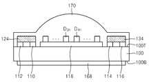
도 1 및 도 2는 본 발명의 기술적 사상에 의한 일부 실시예에 따른 발광 소자 패키지(10)의 요부(要部) 구성을 도시한 평면도들로서, 도 1은 패키지 기판(100)의 상면(100T) 상에 위치하는 일부 구성들을 예시한 평면도이고, 도 2는 패키지 기판(100)의 하면(100B) 상에 위치하는 일부 구성들을 예시한 평면도이다. 설명의 편의를 위해 도 1에서는 렌즈부(도 3 참조, 170)의 도시를 생략하였음을 알려둔다.1 and 2 are plan views showing a main part of a light
도 1 및 도 2를 참조하면, 발광 소자 패키지(10)는 패키지 기판(100)의 상면(100T) 위에서 제1 내지 제5 도전 패턴(110, 112, 114, 116, 118), 제1 정류 회로부(120), 제2 정류 회로부(130), 제1 발광 소자부(140), 및 제2 발광 소자부(150)를 포함할 수 있고, 패키지 기판(100)의 하면(100B) 위에서 제1 내지 제5 하부 도전 패턴(160, 162, 164, 166, 168)을 포함할 수 있다.1 and 2, a light
상기 패키지 기판(100)의 상면(100T) 위에는, 중심에 상기 제5 도전 패턴(118)이 형성될 수 있고, 상기 제5 도전 패턴(118)을 기준으로 일 측(X1 방향)에 상기 제1 및 제2 도전 패턴(110, 112)이 형성될 수 있고, 상기 제5 도전 패턴(118)을 기준으로 다른 일 측(X2 방향)에 상기 제3 및 제4 도전 패턴(114, 116)이 형성될 수 있다.The fifth
일부 실시예들에서, 상기 제5 도전 패턴(118)은 상기 제1 내지 제4 도전 패턴(110, 112, 114, 116)보다 큰 면적을 갖는 사각형의 수평 단면 형상을 가질 수 있다. 상기 제1 내지 제4 도전 패턴(110, 112, 114, 116)은 다각형의 수평 단면 형상을 가질 수 있다. 예컨대, 상기 제1 내지 제4 도전 패턴(110, 112, 114, 116)은 'ㄱ'자의 수평 단면 형상을 가질 수 있다. 그러나, 이에 한정되는 것은 아니고, 상기 제1 내지 제5 도전 패턴(110, 112, 114, 116)은 다양한 수평 단면 형상을 가질 수 있다.In some embodiments, the fifth
상기 제1 및 제2 도전 패턴(110, 112)은 상기 제5 도전 패턴(118)을 기준으로 일 측(X1 방향)에서 서로 대향하도록 배치되어 상기 제1 정류 회로부(120)와 오버랩(overlap)될 수 있다. 마찬가지로, 상기 제3 및 제4 도전 패턴(114, 116)은 상기 제5 도전 패턴(118)을 기준으로 다른 일 측(X2 방향)에서 서로 대향하도록 배치되어 상기 제2 정류 회로부(130)와 오버랩될 수 있다.The first and second
상기 패키지 기판(100)의 하면(100B) 위에는, 중심 영역에 제5 하부 도전 패턴(168)이 형성될 수 있고, 상기 제5 하부 도전 패턴(168)을 기준으로 일 측(Y1 방향)에 상기 제1 및 제3 하부 도전 패턴(160, 164)이 상호 이격되도록 형성될 수 있고, 다른 일 측(Y2 방향)에 상기 제2 및 제4 하부 도전 패턴(162, 166)이 상호 이격되도록 형성될 수 있다.A fifth lower
일부 실시예들에서, 상기 제1 내지 제5 하부 도전 패턴(160, 162, 164, 166, 168)은 사각형의 수평 단면 형상을 가질 수 있다. 상기 제1 내지 제4 하부 도전 패턴(160, 162, 164, 166)은 각각 동일한 면적을 갖는 사각형의 수평 단면 형상을 가질 수 있고, 상기 제5 하부 도전 패턴(168)은 상기 제1 내지 제4 하부 도전 패턴(160, 162, 164, 166)보다 큰 면적을 갖는 사각형의 수평 단면 형상을 가질 수 있다.In some embodiments, the first through fifth lower
일부 실시예들에서, 상기 제1 및 제3 하부 도전 패턴(160, 164)은 서로 접할 수 있고, 상기 제2 및 제4 하부 도전 패턴(162, 166)도 서로 접할 수 있다. 예컨대, 후술되는 바와 같이 인가 전원의 레벨에 따라 상기 제1 정류 회로부(120)와 상기 제2 정류 회로부(130)가 접속되어야 하는 경우(도 8 및 도 10참조), 상기 제1 및 제3 하부 도전 패턴(160, 164)이 서로 접하거나, 또는 상기 제2 및 제4 하부 도전 패턴(162, 166)이 서로 접할 수도 있다.In some embodiments, the first and third bottom
상기 제1 내지 제4 하부 도전 패턴(160, 162, 164, 166)은, 상기 패키지 기판(100)을 관통하여 형성되는 적어도 하나의 관통 전극(V)을 통해 각기 대응하는 상기 제1 내지 제4 도전 패턴(110, 112, 114, 116)과 전기적으로 연결될 수 있다. 이에 따라, 상기 제1 내지 제4 하부 도전 패턴(160, 162, 164, 166)은, 소정의 전원을 인가하기 위한 외부 장치(미도시)와 다양한 방식으로 접속되어, 상기 제1 내지 제4 도전 패턴(110, 112, 114, 116)을 통해 상기 제1 및 제2 정류 회로부(120, 124)로 상기 인가 전원을 전송할 수 있다.The first through fourth lower
상기 패키지 기판(100)의 상면(100T)의 일 측(X1 방향)에서 상기 제1 및 제2 도전 패턴(110, 112) 상에 상기 제1 정류 회로부(120)가 위치할 수 있다. 상기 제5 도전 패턴(118) 상에는 상기 제1 발광 소자부(140)가 위치할 수 있다. 상기 제1 정류 회로부(120)는 상기 제5 도전 패턴(118) 상에 위치하는 상기 제1 발광 소자부(140)와 전기적으로 연결될 수 있다.The first
상기 제1 정류 회로부(120)는 제1 다이오드부(122) 및 제2 다이오드부(124)를 포함할 수 있다. 상기 제1 다이오드부(122) 및 제2 다이오드부(124)는, 동일 기판에 형성되며 일 전극을 공유하는 적어도 둘 이상의 다이오드를 구비할 수 있다.The first
일부 실시예에서, 상기 제1 다이오드부(122)는, 제1 도전형(N형) 기판(미도시)에 제2 도전형(P형) 불순물로 도핑되는 적어도 둘 이상의 불순물 영역들(미도시)이 형성됨에 따라 PN 접합(junction)으로 정의되는 적어도 둘 이상의 다이오드들을 구비할 수 있다. 이 경우, 상기 제1 다이오드부(122)의 다이오드들은 N형 전극을 공유할 수 있다.In some embodiments, the
일부 실시예에서, 상기 제2 다이오드부(124)는 제2 도전형(P형) 기판(미도시)에 제1 도전형(N형) 불순물로 도핑되는 적어도 둘 이상의 불순물 영역들(미도시)이 형성됨에 따라 PN 접합으로 정의되는 적어도 둘 이상의 다이오드들을 구비할 수 있다. 이 경우, 상기 제2 다이오드부(124)의 다이오드들은 P형 전극을 공유할 수 있다. 상기 제1 및 제2 다이오드부(122, 124)에 대해서는 이하에서 도 4 및 도 5를 참조하여 더 자세히 설명한다.In some embodiments, the
상기 제1 및 제2 다이오드부(122, 124) 내에서 다이오드들 각각이 일 전극을 공유하고, 상기 제1 다이오드부(122)의 다이오드들이 상기 제1 및 제2 도전 패턴(110, 112)을 통해 각기 제2 다이오드부(124)의 다이오드들과 전기적으로 연결됨으로써, 상기 제1 정류 회로부(120)는 브릿지 정류 회로로 동작할 수 있다. 이에 따라, 상기 제1 정류 회로부(120)는 상기 제1 및 제2 도전 패턴(110, 112)을 통해 인가되는 교류 전원을 전파(full) 정류하여 상기 제1 발광 소자부(140)로 출력할 수 있다.Each of the diodes in the first and
상기 제1 발광 소자부(140)는 제1 발광 소자 영역(142)과 제2 발광 소자 영역(144)을 포함할 수 있다. 상기 제1 및 제2 발광 소자 영역(142, 144)은 각기 적어도 하나의 발광 소자를 포함할 수 있다. 일부 실시예에서, 상기 제1 및 제2 발광 소자 영역(142, 144)은 각기 n개(n은 자연수)의 발광 소자들(D11 내지 D1n, D21 내지 D2n)을 포함할 수 있다. 그러나, 이에 한정되는 것은 아니고, 상기 제1 및 제2 발광 소자 영역(142, 144)이 각각 상이한 개수의 발광 소자들을 포함할 수도 있다.The first light emitting
일부 실시예에서, 상기 제1 발광 소자 영역(142)의 발광 소자들(D11 내지 D1n)은 서로 직렬 접속되어 하나의 전류 경로를 형성하는 형태로 배치될 수 있다. 그러나 이에 한정되는 것은 아니며, 상기 제1 발광 소자 영역(142)의 발광 소자들(D11 내지 D1n)은 소정 그룹 단위로 직렬 접속되고, 상기 그룹 단위가 병렬 접속되어 복수의 전류 경로를 형성하는 형태로 배치될 수도 있다. 마찬가지로, 상기 제2 발광 소자 영역(144)의 발광 소자들(D21 내지 D2n)은 서로 직렬 접속된 형태로 배치될 수 있으나, 이에 한정되는 것은 아니다. 이에 대해서는, 이하에서 도 6을 참조하여 더 상세히 설명한다.In some embodiments, the light emitting elements D11 to D1n of the first light emitting
일부 실시예에서, 상기 제1 발광 소자 영역(142)의 발광 소자들(D11 내지 D1n)은 상기 제2 발광 소자 영역(144)의 발광 소자들(D21 내지 D2n)과 상호 전기적으로 연결될 수 있다. 즉, 상기 제1 발광 소자 영역(142)의 발광 소자(D1n)와 상기 제2 발광 소자 영역(144)의 발광 소자(D2n)가 연결 부재, 예컨대 와이어(W2)를 통해 전기적으로 연결되어, 상기 제1 발광 소자 영역(142)의 직렬 접속된 발광 소자들(D11 내지 D1n)과 상기 제2 발광 소자 영역(144)의 직렬 접속된 발광 소자들(D21 내지 D2n)을 직렬 접속 시킬 수 있다. 그러나, 이에 한정되는 것은 아니고, 상기 제5 도전 패턴(118) 상에 형성되는 소정의 패턴(미도시)을 통해 상기 제1 발광 소자 영역(142)의 발광 소자(D1n)와 상기 제2 발광 소자 영역(144)의 발광 소자(D2n)가 전기적으로 연결될 수도 있다.In some embodiments, the light emitting elements D11 to D1n of the first light emitting
상기 제1 정류 회로부(120)와 상기 제1 발광 소자부(140)는 연결 부재, 예컨대 와이어(W1)를 통해 상호 전기적으로 연결될 수 있다. 일부 실시예에서, 상기 제1 정류 회로부(120)의 제1 다이오드부(122)가 상기 제1 발광 소자 영역(142)의 발광 소자(D11)와 전기적으로 연결되고, 상기 제1 정류 회로부(120)의 제2 다이오드부(124)가 상기 제2 발광 소자 영역(144)의 발광 소자(D21)와 전기적으로 연결될 수 있다. 이에 따라, 상기 제1 정류 회로부(120)는 상기 제1 및 제2 도전 패턴(110, 112)을 통해 제공되는 인가 전원, 예컨대 교류 전원을 정류하여 상기 제1 발광 소자부(140)에서 직렬 접속된 발광 소자들(D11 내지 D1n, D21 내지 D2n)로 전송할 수 있다. 상기 제1 발광 소자부(140)의 발광 소자들(D11 내지 D1n, D21 내지 D2n)은 상기 제1 정류 회로부(120)로부터 전송되는 구동 전원, 예컨대 직류 전류에 응답하여 빛을 방출할 수 있다.The first
상기 패키지 기판(100)의 상면(100T)의 다른 일 측(X2 방향)에서 상기 제3 및 제4 도전 패턴(114, 116) 상에 상기 제2 정류 회로부(130)가 위치할 수 있다. 상기 제5 도전 패턴(118) 상에는 상기 제2 발광 소자부(150)가 더 위치할 수 있다. 상기 제2 정류 회로부(130)는 상기 제5 도전 패턴(118) 상에 위치하는 상기 제2 발광 소자부(150)와 전기적으로 연결될 수 있다.The second
상기 제2 정류 회로부(130)는 제3 다이오드부(132) 및 제4 다이오드부(134)를 포함할 수 있다. 상기 제3 다이오드부(132) 및 상기 제4 다이오드부(134)는, 각기 상기 제1 다이오드부(122) 및 상기 제2 다이오드부(124)와 실질적으로 동일한 소자들일 수 있다. 즉, 상기 제3 다이오드부(132)는 하나의 기판에 형성되 N형 전극을 공유하는 적어도 둘 이상의 다이오드들을 구비할 수 있으며, 상기 제4 다이오드부(134)는 하나의 기판에 형성되며 P형 전극을 공유하는 적어도 둘 이상의 다이오드들을 구비할 수 있다.The second
상기 제1 정류 회로부(120)와 마찬가지로, 상기 제3 및 제4 다이오드부(132, 134) 내에서 다이오드들 각각이 일 전극을 공유하고, 상기 제3 다이오드부(132) 내의 접합 다이오드들이 상기 제3 및 제4 도전 패턴(114, 116)을 통해 각기 제4 다이오드부(134) 내의 다이오드들과 전기적으로 연결됨으로써, 상기 제2 정류 회로부(130)는 브릿지 정류 회로로 동작할 수 있다. 이에 따라, 상기 제2 정류 회로부(130)는 상기 제3 및 제4 도전 패턴(114, 116)을 통해 인가되는 교류 전원을 전파 정류하여 상기 제2 발광 소자부(150)로 출력할 수 있다.The diodes in the third and
상기 제2 발광 소자부(150)는 제3 발광 소자 영역(152)과 제4 발광 소자 영역(154)을 포함할 수 있다. 상기 제3 발광 소자 영역(152)과 상기 제4 발광 소자 영역(154)은 상호 전기적으로 연결될 수 있다.The second light emitting
상기 제3 발광 소자 영역(152) 및 상기 제4 발광 소자 영역(154)은, 각기 상기 제1 발광 소자 영역(142) 및 상기 제2 발광 소자 영역(142)과 실질적으로 동일한 구성을 가질 수 있다 즉, 상기 제3 및 제4 발광 소자 영역들(152, 154)은 각기 서로 직렬 접속된 n개(n은 자연수)의 발광 소자들(D31 내지 D3n, D41 내지 D4n)을 포함할 수 있다. 그리고, 상기 제3 발광 소자 영역(152)의 발광 소자(D3n)와 상기 제4 발광 소자 영역(154)의 발광 소자(D4n)가 연결 부재, 예컨대 와이어(W2)를 통해 전기적으로 연결되어, 발광 소자들(D31 내지 D3n, D41 내지 D4n)이 단일 전류 경로를 형성할 수 있다.The third light emitting
상기 제2 정류 회로부(130)와 상기 제2 발광 소자부(150)도, 상기 제1 정류 회로부(120) 및 상기 제1 발광 소자부(140)와 마찬가지로 연결 부재, 예컨대 와이어(W1)를 통해 상호 전기적으로 연결될 수 있다. 이에 따라, 상기 제2 정류 회로부(120)도 상기 제3 및 제4 도전 패턴(114, 116)을 통해 제공되는 인가 전원, 예컨대 교류 전원을 정류하여 상기 제2 발광 소자부(150)에서 직렬 접속된 발광 소자들(D31 내지 D3n, D41 내지 D4n)로 전송할 수 있다. 상기 제2 발광 소자부(150)의 발광 소자들(D31 내지 D3n, D41 내지 D4n)은 상기 제2 정류 회로부(130)로부터 전송되는 구동 전원, 예컨대 직류 전류에 응답하여 빛을 방출할 수 있다.The second
이와 같이, 본 발명의 기술적 사상에 따른 발광 소자 패키지(10)는 상기 제1 및 제2 정류 회로부(120, 130)에 각기 대응하여 상기 제1 및 제2 발광 소자부(140, 150)의 발광 소자들이 독립적으로 구동되는 구조를 가질 수 있다.As described above, the light emitting
도 3은 도 1의 발광 소자 패키지(10)를 A - A' 선을 따라 절단한 단면도이다. 도 3을 설명함에 있어서, 도 1 및 도 2에서와 동일한 참조 부호는 동일 부재를 나타내며, 여기서는 설명의 간략화를 위하여 이들에 대한 중복되는 설명은 생략한다.FIG. 3 is a cross-sectional view of the light emitting
도 1 내지 도 3을 참조하면, 상기 패키지 기판(100)의 상면(100T)에 상기 제1 내지 제5 도전 패턴(110, 112, 114, 116, 118)이 상호 이격되어 형성될 수 있고, 상기 패키지 기판(100)의 하면(100B)에 상기 제5 하부 도전 패턴(168)이 형성될 수 있다.1 to 3, the first to fifth
일부 실시예들에서, 상기 패키지 기판(100)은 절연성 기판일 수 있다. 예컨대, 상기 패키지 기판(100)은 실리콘 기판, 세라믹 기판, 알루미늄 나이트라이드(AlN) 기판, 사파이어(Al2O3) 기판, FR4 기판 등 일 수 있다.In some embodiments, the
일부 실시예들에서, 상기 제1 내지 제5 도전 패턴(110, 112, 114, 116, 118), 및 상기 제5 하부 도전 패턴(168)은 전기 전도성이 우수하며 접합이 가능한 금속 물질막으로 이루어질 수 있다. 상기 금속 물질막은, 예컨대 Cu, Au, Ag, Al, Ni, Cr 등의 금속 물질 중 적어도 하나를 포함할 수 있다. 도 3에서 도시되지는 않았으나, 제1 내지 제4 하부 도전 패턴(160, 162, 164, 166) 또한 앞서 예시된 금속 물질막으로 이루어질 수 있다.In some embodiments, the first through fifth
상기 제1 및 제2 도전 패턴(110, 112) 상에는 제2 다이오드부(124)가 위치할 수 있고, 상기 제3 및 제4 도전 패턴(114, 116) 상에는 제4 다이오드부(134)가 위치할 수 있고, 상기 제5 도전 패턴(118) 상에는 상기 제2 발광 소자 영역(142)의 발광 소자(D2n)들과 상기 제4 발광 소자 영역(152)의 발광 소자(D4n)들이 위치할 수 있다.A
일부 실시예들에서, 상기 발광 소자들(D2, D4)은 수평 전극구조, 수직 전극구조, 또는 수직수평 전극구조를 채용할 수 있다.In some embodiments, the light emitting elements D2 and D4 may employ a horizontal electrode structure, a vertical electrode structure, or a vertical and horizontal electrode structure.
상기 패키지 기판(100) 위에는, 상기 패키지 기판(100)의 상면(100T)을 덮되 상기 제1 다이오드부(124), 상기 제3 다이오드부(134), 및 발광 소자들(D2n, D4n)을 감싸는 렌즈부(170)가 구비될 수 있다.The
일부 실시예들에서, 상기 렌즈부(170) 내부는 실리콘 수지, 에폭시 수지, 플라스틱, 또는 유리로 채워질 수 있다. 다른 일부 실시예들에서, 상기 렌즈부(170) 내부에 굴절 부재(미도시)가 포함될 수도 있다. 상기 굴절 부재(미도시)는 상기 발광 소자(D2, D4)들로부터 방출되는 빛을 굴절 또는 반사시킬 수 있다. 다른 일부 실시예들에서, 상기 렌즈부(170)는 형광체(미도시)를 포함할 수 있다. 상기 형광체는 황색 형광체, 녹색 형광체, 적색 형광체, 및 청색 형광체 중 적어도 하나를 포함할 수 있다.In some embodiments, the interior of the
도 4는 도 1의 발광 소자 패키지(10)를 B - B' 선을 따라 절단한 단면도이다. 도 4를 설명함에 있어서, 도 1 내지 도 3에서와 동일한 참조 부호는 동일 부재를 나타내며, 여기서는 설명의 간략화를 위하여 이들에 대한 중복되는 설명은 생략하고, 제1 다이오드부(122)와 발광 소자(D11)를 중심으로 설명한다. 한편, 도 4에서는 상기 발광 소자(D11)가 수평 전극구조를 갖고 플립 칩 형태로 상기 패키지 기판(100) 상에 실장되는 것으로 도시되고 있으나 이에 한정되는 것은 아니며, 상기 발광 소자(D11)는 수직 전극구조, 수직수평 전극 구조를 가지고 다양한 방식으로 상기 패키지 기판(100) 상에 실장될 수 있다.4 is a cross-sectional view of the light emitting
도 1 내지 도 4를 참조하면, 상기 제1 다이오드부(122)는 제1 도전형 기판(122_1)을 포함할 수 있다. 일부 실시예에서, 상기 제1 도전형 기판(122_1)은 절연성 기판 또는 실리콘, 실리콘 카바이드 갈륨 나이트라이드 등의 도전성 기판의 적어도 일부가 제1 도전형 불순물, 예컨대 N형 불순물로 도핑된 기판일 수 있다.Referring to FIGS. 1 to 4, the
상기 제1 도전형 기판(122_1)의 하면(122_1B)에는 제1 공통 전극(122_2)이 형성될 수 있다. 일부 실시예에서, 상기 제1 공통 전극(122_2)은 전기 전도성이 전도성이 우수한 금속 물질막으로 이루어질 수 있다. 상기 금속 물질막은, 예컨대 Cu, Au, Ag, Al, Ni, Cr 등의 금속 물질 중 적어도 하나를 포함할 수 있다.A first common electrode 122_2 may be formed on a lower surface 122_1B of the first conductive type substrate 122_1. In some embodiments, the first common electrode 122_2 may be made of a metal material film having good electrical conductivity. The metal material layer may include at least one of metal materials such as Cu, Au, Ag, Al, Ni, and Cr.
상기 제1 도전형 기판(122_1)에는 상기 제1 도전형 기판(122_1)의 상면으로부터 소정의 깊이를 갖되 상호 이격되는 제1 및 제2 불순물 영역(122_3, 122_4)이 형성될 수 있다. 일부 실시예에서, 상기 제1 및 제2 불순물 영역(122_3, 122_4)은, 각각 제2 도전형 불순물, 예컨대 P형 불순물로 도핑된 영역일 수 있다. 이에 따라, 상기 제1 불순물 영역(122_3)과 상기 제1 도전형 기판(122_1)이 형성하는 PN 접합이 제1 다이오드(RD1)를 정의하고, 상기 제2 불순물 영역(122_4)과 상기 제1 도전형 기판(122_1)이 형성하는 PN 접합이 제2 다이오드(RD2)를 정의한다.The first conductive type substrate 122_1 may have first and second impurity regions 122_3 and 122_4 spaced apart from the upper surface of the first conductive type substrate 122_1 by a predetermined depth. In some embodiments, the first and second impurity regions 122_3 and 122_4 may be regions doped with a second conductivity type impurity, for example, a P type impurity, respectively. Accordingly, the PN junction formed by the first impurity region 122_3 and the first conductive type substrate 122_1 defines a first diode RD1, and the second impurity region 122_4 and the first conductivity type Type substrate 122_1 defines a second diode RD2.
상기 제1 및 제2 불순물 영역(122_3, 122_4) 상에는 각각 제1 전극(122_5)이 형성될 수 있고, 상기 제1 전극(122_5)은 절연막(122_6)에 의해 상호 분리될 수 있다. 일부 실시예에서, 상기 제1 전극들(122_5)은 전기 전도성이 우수하며 상기 제1 및 제2 도전 패턴(110, 112)과 접합이 가능한 금속 물질막으로 이루어질 수 있다. 상기 금속 물질막은, 예컨대 Cu, Ag, Al, Ni, Cr, V, Au, Sn, Pb, Ag, In, Ge, Si 중 적어도 하나를 포함할 수 있다. 일부 실시예에서, 상기 절연막(122_6)은 절연 물질, 예컨대 실리콘 산화물, 실리콘 질화물, 실리콘 산질화물 중 어느 하나로 이루어질 수 있다.The first electrode 122_5 may be formed on the first and second impurity regions 122_3 and 122_4 and the first electrode 122_5 may be separated from each other by the insulating layer 122_6. In some embodiments, the first electrodes 122_5 may be formed of a metal material layer having good electrical conductivity and capable of bonding with the first and second
이와 같이, 상기 제1 다이오드부(122)는 상기 제1 도전형 기판(122_1)내에 형성되고, 상기 제1 공통 전극(122_2)을 공유하는 상기 제1 다이오드(RD1) 및 상기 제2 다이오드(RD2)를 구비할 수 있다.As such, the
상기 제1 다이오드부(122)는, 상기 제1 도전형 기판(122_1)의 상면(122_1T)이 상기 패키지 기판(100)의 상면(100T)에 대향하도록 위치하여 상기 제1 전극들(122_5)과 상기 제1 및 제2 도전 패턴(110, 112)이 상호 접합되는 플립 칩 형태로 상기 패키지 기판(100)에 실장될 수 있다. 상기 제1 다이오드(RD1) 상의 제1 전극(122_5)과 상기 제2 도전 패턴(112) 사이, 상기 제2 다이오드(RD2) 상의 제1 전극(122_5)과 제1 도전 패턴(110) 사이에는 접합 부재(122_7), 예컨대 솔더 등이 개재될 수 있다.The
상기 발광 소자(D11)는 성장 기판(170)의 일면에 제1 반도체층(171), 발광층(172), 제2 반도체층(173)이 순차적으로 적층된 발광 구조체(LES)를 구비할 수 있다. 일부 실시예에서, 상기 성장 기판(170)의 일면과 이에 반대되는 면에는 소정 거칠기의 요철이 형성될 수 있다. 일부 실시예에서, 상기 제1 반도체층(171), 상기 발광층(172), 상기 제2 반도체층(173)은, 3족 질화물 반도체를 포함할 수 있다.The light emitting device D11 may include a light emitting structure LES in which a
상기 발광 소자(D11)는 상기 발광 구조체(LES)의 적어도 일부를 제거하여 노출되는 상기 제1 반도체층(171) 상에 형성된 제1 전극 패드(174), 상기 제2 반도체층(173) 상에 형성된 제2 전극 패드(175)를 구비할 수 있다. 일부 실시예에서, 상기 제1 전극 패드(174) 및 상기 제2 전극 패드(175)는 ITO(Indium Tin Oxide), Cu, Ni, Cr, Au, Ti, Pt, Al, V, W, Mo, Ag 중 적어도 하나를 포함할 수 있다.The light emitting device D11 includes a
상기 제5 도전 패턴(118) 상에는 상기 제1 및 제2 전극 패드(174, 175)에 대응하는 제1 및 제2 본딩 패턴(177, 178)이 형성될 수 있으며, 상기 발광 소자(D11)는 상기 제1 및 제2 전극 패드(174, 175)가 접합 부재(176), 예컨대 솔더 등을 매개로 하여 각기 제1 및 제2 본딩 패턴(177, 178)에 접합되는 플립 칩 형태로 상기 패키지 기판(100) 상에 실장될 수 있다.Wherein the fifth
상기 제1 다이오드부(122)의 제1 공통 전극(122_2)과 상기 본딩 패턴(177)은 연결 부재, 예컨대 와이어(W1)를 통해 전기적으로 연결될 수 있으며, 이를 통해 상기 제1 다이오드부(122)와 상기 발광 소자(D11)가 전기적으로 연결될 수 있다.The first common electrode 122_2 of the
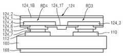
도 5는 도 1의 발광 소자 패키지(10)를 C - C' 선을 따라 절단한 단면도이다. 도 5를 설명함에 있어서, 도 1 내지 도 4에서와 동일하거나 대응되는 참조 부호는 동일하거나 대응되는 부재를 나타내며, 여기서는 설명의 간략화를 위하여 이들에 대한 중복되는 설명은 생략하고 제2 다이오드부(124)를 중심으로 설명한다.5 is a cross-sectional view of the light emitting
도 1 내지 도 5를 참조하면, 상기 제2 다이오드부(124)는 제2 도전형 기판(124_1)을 포함할 수 있다. 일부 실시예에서, 상기 제2 도전형 기판(124_1)은 절연성 기판 또는 도전성 기판의 적어도 일부가 제2 도전형 불순물, 예컨대 P형 불순물로 도핑된 기판일 수 있다.1 to 5, the
상기 제2 도전형 기판(124_1)의 하면(124_1B)에는 제2 공통 전극(124_2)이 형성될 수 있다. 상기 제2 공통 전극(124_2)은 상기 제1 공통 전극(122_2)에서 예시한 물질들로 이루어질 수 있다.A second common electrode 124_2 may be formed on the lower surface 124_1B of the second conductive type substrate 124_1. The second common electrode 124_2 may be formed of the materials exemplified in the first common electrode 122_2.
상기 제2 도전형 기판(124_1)에는 상기 제2 도전형 기판(124_1)의 상면으로부터 소정의 깊이를 갖되 상호 이격되는 제3 및 제4 불순물 영역(124_3, 124_4)이 형성될 수 있다. 일부 실시예에서, 상기 제3 및 제4 불순물 영역(124_3, 124_4)은, 각각 제1 도전형 불순물, 예컨대 N형 불순물로 도핑된 영역일 수 있다. 이에 따라, 상기 제3 불순물 영역(124_3)과 상기 제2 도전형 기판(124_1)이 형성하는 PN 접합이 제3 다이오드(RD3)를 정의하고, 상기 제4 불순물 영역(124_4)과 상기 제2 도전형 기판(124_1)이 형성하는 PN 접합이 제4 다이오드(RD4)를 정의한다.Third and fourth impurity regions 124_3 and 124_4 may be formed on the second conductive type substrate 124_1 to have a predetermined depth from the upper surface of the second conductive type substrate 124_1. In some embodiments, the third and fourth impurity regions 124_3 and 124_4 may be regions doped with a first conductivity type impurity, for example, an N type impurity, respectively. Accordingly, the PN junction formed by the third impurity region 124_3 and the second conductive type substrate 124_1 defines a third diode RD3, and the fourth impurity region 124_4 and the second conductivity type Type substrate 124_1 defines a fourth diode RD4.
상기 제3 및 제4 불순물 영역(124_3, 124_4) 상에는 각각 제2 전극들(124_5)이 형성될 수 있고, 상기 제2 전극들(124_5)은 절연막(124_6)에 의해 상호 분리될 수 있다. 상기 제2 전극들(124_5) 및 상기 절연막(124_6)은 상기 제1 전극들(122_5) 및 절연막(122_6)을 구성하는 물질로 예시한 물질들로 이루어질 수 있다.The second electrodes 124_5 may be formed on the third and fourth impurity regions 124_3 and 124_4 and the second electrodes 124_5 may be separated from each other by the insulating layer 124_6. The second electrodes 124_5 and the insulating layer 124_6 may be formed of materials exemplified as materials constituting the first electrodes 122_5 and the insulating layer 122_6.
이를 통해, 상기 제2 다이오드부(124)는 상기 제3 다이오드(RD3) 및 상기 제4 다이오드(RD4)가 상기 제2 도전형 기판(124_1)내에 구비되고, 상기 제2 공통 전극(124_2)을 공유하는 단일 소자로 구성될 수 있다.Accordingly, the
상기 제2 다이오드부(124)는, 상기 제2 도전형 기판(124_1)의 상면(124_1T)이 상기 패키지 기판(100)의 상면(100T)에 대향하도록 위치하여 상기 제2 전극들(124_5)과 상기 제1 및 제2 도전 패턴(110, 112)이 상호 접합되는 플립 칩 형태로 상기 패키지 기판(100)에 실장될 수 있다. 상기 제3 다이오드(RD3) 상의 제2 전극(124_5)과 상기 제1 도전 패턴(110) 사이, 상기 제4 다이오드(RD4) 상의 제2 전극(124_5)과 상기 제2 도전 패턴(112) 사이에는 접합 부재(124_7), 예컨대 솔더 등이 개재될 수 있다.The
도 5에 도시되지는 않았으나, 도 4에서 도시한 상기 제1 다이오드부(122)와 상기 발광 소자(D11)의 접속 방식과 유사하게 상기 제2 다이오드부(124)의 제2 공통 전극(124_2)은 상기 발광 소자(D21)와 전기적으로 연결될 수 있다.Although not shown in FIG. 5, similar to the connection mode of the
상기 도 4 및 도 5를 참조하여 설명한 바와 같이, 상기 제1 정류 회로부(122)는, 상기 제2 다이오드(RD2)와 상기 제3 다이오드(RD3)가 상기 제1 도전 패턴(110)에 연결되고, 상기 제1 다이오드(RD1)와 상기 제4 다이오드(RD4)가 상기 제2 도전 패턴(112)에 연결되고, 상기 제1 다이오드(RD1)와 상기 제2 다이오드(RD2)가 제1 공통 전극(122_2)을 공유하고, 상기 제3 다이오드(RD3)와 상기 제4 다이오드(RD4)가 제2 공통 전극(124_2)을 공유함으로써, 브릿지 정류 회로로 동작할 수 있다.4 and 5, the first
한편, 상기 제2 정류 회로부(130)의 제3 및 제4 다이오드부(132, 134)는 각기 앞서 설명한 상기 제1 및 제2 다이오드부(122, 124)와 실질적으로 동일한 구성을 가지므로, 상기 제2 정류 회로부(130) 또한 브릿지 정류 회로로 동작 할 수 있다.Since the third and
이와 같이, 본원 발명에 따른 제1 정류 회로부(120) 및 제2 정류 회로부(130)는, 교류 전원을 사용하여 직접 발광 소자들을 구동 시키기 위해 패키지 내에 독립적인 네 개의 다이오드 소자들로 브릿지 정류 회로를 구현하는 경우에 비하여, 두 개의 다이오드부들만으로 브릿지 정류 회로를 구현할 수 있어 정류 회로가 차지하는 면적이 감소될 수 있다.As described above, the first
이에 따라, 발광 소자 패키지(10)의 전체의 크기를 최소화할 수 있으며, 상기 패키지 기판(100) 내에서 발광 소자들이 배치되는 면적을 상대적으로 증가시킬 수 있어 발광 소자 패키지(10)의 출력 확보가 용이할 수 있다. 또한, 와이어 본딩을 통해 독립적인 네 개의 다이오드 소자들을 각기 전기적으로 연결시키는 경우에 비하여 배선이 용이하여 발광 소자 패키지(10) 제조 시 불량 발생을 방지할 수 있으며, 발광 소자 패키지(10) 제조 공정을 간소화 시킬 수 있다.Accordingly, the entire size of the light emitting
도 6은 도 1의 발광 소자 패키지(10)에서 제1 발광 소자부(140)의 일부 구성들을 도시한 평면도로서, 상기 제1 발광 소자부(140)의 제1 발광 소자 영역(142)에서 발광 소자들(D11 내지 D15)의 직렬 접속 방식에 대한 일 실시예를 설명하기 위한 도면이다. 도 6을 설명함에 있어서, 도 1 내지 도 5에서와 동일한 참조 부호는 동일 부재를 나타내며, 여기서는 설명의 간략화를 위하여 이들에 대한 중복되는 설명은 생략한다. 한편, 도 6에서는 상기 제1 발광 소자 영역(142)에 15개의 발광 소자들이 구비되는 것으로 도시되고 있으나 이에 한정되는 것은 아니다.FIG. 6 is a plan view of a part of the first light emitting
도 1 내지 도 6을 참조하면, 상기 제1 발광 소자 영역(142) 내의 상기 제5 도전 패턴(118) 상에는 플립 칩 구조로 실장되는 상기 발광 소자들(D11 내지 D15) 각각에 대응하여 상기 제1 및 제2 본딩 패턴(177, 178)이 형성될 수 있다.Referring to FIGS. 1 to 6, on the fifth
상기 제1 및 제2 본딩 패턴(177, 178)은 각기 상기 발광 소자들(D11 내지 D15)의 전극 패드들과 접속되며, 상기 발광 소자들(D11 내지 D15)의 실장 방식에 따라 다양한 형상을 가질 수 있다.The first and
상기 발광 소자들(D11 내지 D15)은, 각기 다른 발광 소자의 전극 패드와 접속되는 제1 및 제2 본딩 패턴 사이, 예컨대 제1 본딩 패턴(177_2)과 제2 본딩 패턴(178_1) 사이를 도전 패턴(P)을 통해 연결함으로써, 상호 직렬 접속될 수 있다. 한편, 상기 발광 소자(D11)의 제1 본딩 패턴(177_1)은 와이어(W1)를 통해 제1 정류 회로부(100)와 전기적으로 연결되고, 상기 발광 소자(D15)의 제2 본딩 패턴(178_15)은 와이어(W2)를 통해 제2 발광 소자 영역(144)의 발광 소자와 전기적으로 연결될 수 있다.The light emitting elements D11 to D15 are disposed between the first and second bonding patterns connected to the electrode pads of the different light emitting elements, for example, between the first bonding pattern 177_2 and the second bonding pattern 178_1 They can be connected in series by connecting them through the conductive pattern P. The first bonding pattern 177_1 of the light emitting device D11 is electrically connected to the first
도 6에 도시 되지는 않았으나, 제2 내지 제4 발광 소자 영역(144, 152, 154)의 발광 소자들도 상기 제1 발광 소자 영역(142)에서와 유사한 방식으로 접속될 수 있다.Although not shown in FIG. 6, the light emitting elements of the second through fourth light emitting
도 7은 도 1의 발광 소자 패키지(10)의 일부 구성들 사이의 전기적 연결 상태를 개략적으로 나타낸 회로도이다. 도 7을 설명함에 있어서, 도 1에서와 동일한 참조 부호는 동일한 부재를 나타내며, 여기서는 설명의 간략화를 위하여 이들에 대한 중복되는 설명은 생략하고 상기 제1 정류 회로부(120), 제2 정류 회로부(130), 제1 발광 소자부(140), 제2 발광 소자부(150)를 회로적인 개념으로 설명한다. 한편, 도 7에 도시된 발광 소자 패키지(10)는, 전원부(미도시)에 상기 제1 및 제2 정류 회로부(120, 130)가 병렬적으로 접속되는 경우를 나타낸다.7 is a circuit diagram schematically showing an electrical connection state between some configurations of the light emitting
도 1 및 도 7을 참조하면, 상기 제1 정류 회로부(120)는 전원부(미도시)로부터 소정의 인가 전원(VAC), 예컨대 100V 내지 120V 레벨의 교류 전압을 수신하여 제1 구동 전원(DI1), 예컨대 직류 전류를 생성할 수 있다.1 and 7, the first
상기 제1 정류 회로부(120)는 제1 입력 노드(IN1)와 제1 공통 노드(CN1) 사이에 위치하는 제1 다이오드(RD1), 상기 제1 공통 노드(CN1)와 제2 입력 노드(IN2) 사이에 위치하는 제2 다이오드(RD2), 상기 제2 입력 노드(IN2)와 제2 공통 노드(CN2) 사이에 위치하는 제3 다이오드(RD3), 상기 제2 공통 노드(CN2)와 상기 제1 입력 노드(IN1) 사이에 위치하는 제4 다이오드(RD4)를 포함할 수 있다. 한편, 도 7에서는 상기 노드들 사이에 각기 하나의 다이오드가 위치하는 것으로 도시되고 있으나, 상기 노드들 사이에는 필요로 하는 역방향 전압 특성 등에 따라 적어도 둘 이상의 다이오드들이 위치할 수도 있다.The first
상기 제1 정류 회로부(120)는, 상기 제1 입력 노드(IN1)와 상기 제2 입력 노드(IN2) 사이에 인가되는 상기 인가 전원(VAC)의 방향에 따라 상기 제1 다이오드(RD1)와 상기 제3 다이오드(RD3)가 턴온되거나 상기 제2 다이오드(RD2)와 상기 제4 다이오드(RD4)가 턴온되어, 상기 인가 전원(VAC)을 전파(full wave) 정류한 상기 제1 구동 전원(DI1)을 상기 제1 발광 소자부(140)로 출력할 수 있다.The first
상기 제1 발광 소자부(140)는 상기 제1 구동 전원(DI1)을 수신하여 빛을 방출할 수 있으며, 상기 제1 발광 소자부(140)는 상호 직렬 접속된 발광 소자들(D11 내지 D21)을 포함할 수 있다.The first light emitting
상기 제2 정류 회로부(130)는 상기 인가 전원(VAC)을 수신하여 제2 구동 전원(DI2)을 생성할 수 있다.The
상기 제2 정류 회로부(130)는 제3 입력 노드(IN3)와 제3 공통 노드(CN3) 사이에 위치하는 제5 다이오드(RD5), 상기 제3 공통 노드(CN3)와 제4 입력 노드(IN4) 사이에 위치하는 제6 다이오드(RD6), 상기 제4 입력 노드(IN4)와 제4 공통 노드(CN4) 사이에 위치하는 제7 다이오드(RD7), 상기 제4 공통 노드(CN4)와 상기 제4 입력 노드(IN4) 사이에 위치하는 제8 다이오드(RD8)를 포함할 수 있다. 일부 실시예에서는, 필요로 하는 역방향 전압 특성에 따라 상기 노드들 사이에는 적어도 둘 이상의 다이오드들이 위치할 수도 있다.The second
상기 제2 정류 회로부(130)는, 상기 제3 입력 노드(IN3)와 상기 제4 입력 노드(IN4) 사이에 인가되는 상기 인가 전원(VAC)의 방향에 따라, 상기 제5 다이오드(RD5)와 상기 제7 다이오드(RD7)가 턴온되거나 상기 제6 다이오드(RD6)와 상기 제8 다이오드(RD8)가 턴온되어, 상기 인가 전원(VAC)을 전파 정류한 상기 제2 구동 전원(DI2)을 상기 제2 발광 소자부(150)로 출력할 수 있다.The second
상기 제2 발광 소자부(150)는 제2 구동 전원(DI2)을 수신하여 빛을 방출할 수 있으며, 상기 제1 발광 소자부(140)는 상호 직렬 접속된 발광 소자들(D31 내지 D41)을 포함할 수 있다.The second light emitting
도 7에 도시된 바와 같이, 본 발명의 기술적 사상에 따른 발광 소자 패키지(10)는, 상기 전원부에 병렬적으로 접속된 상기 제1 및 제2 정류 회로부(120, 130)가 출력하는 각각의 제1 및 제2 구동 전원(DI1, DI2)에 응답하여, 상기 제1 발광 소자부(140)의 발광 소자들(D11 내지 D21)과 상기 제2 발광 소자부(150)의 발광 소자들(D31 내지 D41)이 독립적으로 구동되는 회로를 가질 수 있다.7, the light emitting
도 7에 도시된 예와는 반대로, 상기 제1 및 제2 정류 회로부(120, 130)가 직렬적으로 전원부에 접속되는 경우(도 8에서 경로 제어부(360)가 생략되는 경우 참조), 본 발명의 기술적 사상에 따른 발광 소자 패키지(10)는 상기 제1 발광 소자부(140)의 발광 소자들(D11 내지 D21)과 상기 제2 발광 소자부(150)의 발광 소자들(D31 내지 D41)이 상기 제1 및 제2 정류 회로부(120, 130)가 출력하는 동일한 구동 전원에 응답하여 구동되는 회로를 가질 수도 있다. 이 경우, 상기 전원부는 220V 내지 240V 레벨의 인가 전원(VAC)을 상기 제1 및 제2 정류 회로부(120, 130)로 제공할 수 있다.In contrast to the example shown in FIG. 7, when the first and second
이와 같이, 본원 발명에 따른 발광 소자 패키지(10)는 두 개의 정류 회로부와 이들에 각각 연결되는 발광 소자부들을 구비하고 상기 두 개의 정류 회로부들을 전원부와 직렬적 또는 병렬적으로 접속시킴으로써, 다양한 레벨의 교류 전원을 직접 이용하여 구동될 수 있다.As described above, the light emitting
도 8은 본 발명의 기술적 사상에 의한 일부 실시예에 따른 발광 장치(2)의 요부 구성들 사이의 전기적 연결 상태를 개략적으로 나타낸 회로도이고, 도 9는 도 8의 발광 장치(20)의 구동 시 형성되는 전류 루프의 일 예를 설명하기 위한 도면이다. 도 8 및 도 9를 설명함에 있어서, 도 7에서와 동일하거나 대응되는 참조 부호는 동일하거나 대응되는 부재를 나타내며, 여기서는 설명의 간략화를 위하여 이들에 대한 중복되는 설명은 생략하고 차이점을 중심으로 설명한다.FIG. 8 is a circuit diagram schematically showing an electrical connection state between the recesses of the light emitting device 2 according to some embodiments of the technical idea of the present invention. FIG. 9 is a cross- Fig. 7 is a view for explaining an example of a current loop to be formed. 8 and 9, the same or corresponding reference numerals as those in FIG. 7 denote the same or corresponding members, and overlapping descriptions thereof will be omitted for the sake of simplicity, and the differences will be mainly described .
상기 발광 장치(20)는 제1 정류 회로부(220), 제2 정류 회로부(230), 제1 발광 소자부(240), 제2 발광 소자부(250), 경로 제어부(260), 제1 레벨 제어부(270), 및 제2 레벨 제어부(280)를 포함할 수 있다. 상기 발광 장치(20)는, 예컨대, 220V 내지 240V 레벨의 인가 전원(VAC)을 제공하는 전원부(미도시)에 의해 구동 될 수 있다.The
상기 제1 정류 회로부(220)는 상기 제2 정류 회로부(230)와 직렬 접속될 수 있다. 상세하게는, 상기 제1 정류 회로부(220)의 제2 입력 노드(IN2)와 상기 제2 정류 회로부(230)의 제3 입력 노드(IN3)가 상기 전원부를 통해 연결되고, 상기 제1 정류 회로부(220)의 제1 입력 노드(IN1)와 상기 제2 정류 회로부(230)의 제4 입력 노드(IN4)가 전기적으로 연결되어, 상기 제1 정류 회로부(220)와 상기 제2 정류 회로부(230)가 직렬적으로 접속될 수 있다.The first
상기 경로 제어부(260)는 상기 제1 정류 회로부(220)와 병렬 접속될 수 있다. 상세하게는, 상기 경로 제어부(260)는 상기 제1 정류 회로부(220)의 제1 입력 노드(IN1)와 제2 입력 노드(IN2) 사이에 접속될 수 있다. 일부 실시예에서, 상기 경로 제어부(260)는 커패시터(C1)로 구성될 수 있으나 이에 한정되는 것은 아니고, 요구되는 임피던스 레벨에 따라 추가적으로 수동 소자, 예컨대 저항 또는 커패시터가 구비될 수도 있다.The path control
상기 경로 제어부(260)는 상기 인가 전원(VAC)이 상기 제1 정류 회로부(220) 만을 통해서 제2 정류 회로부(230)로 전송되지 않도록 상기 인가 전원(VAC)의 경로를 제어할 수 있다. 예컨대, 상기 경로 제어부(260)의 임피던스 레벨이 상기 제1 정류 회로부(220)의 임피던스 레벨보다 매우 작은 경우, 상기 인가 전원(VAC)의 대부분을 상기 경로 제어부(260)를 통해서만 제2 정류 회로부(230)로 전송되도록 할 수 있다.The
이를 통해, 도 9 에 도시된 바와 같이, 상기 발광 장치(20) 내에는 상기 인가 전원(VAC)이 상기 경로 제어부(260)를 따르는 전류 루프(I)와 상기 제1 정류 회로부(220)를 따르는 전류 루프(II)가 형성될 수 있다.9, the power supply VAC is supplied to the
이와 같이, 상기 경로 제어부(260)를 구비하여 전류 루프(I)를 추가함으로써, 상기 발광 장치(20)에서 발광 소자들의 총 출력 전류(IOT)의 레벨과 위상이 조절될 수 있다. 이에 대해서는 이하에서 도 12를 참조하여 설명한다.Thus, by adding the current loop I with the
상기 제1 레벨 제어부(270)는 상기 제1 정류 회로부(220)와 직렬 접속될 수 있다. 상세하게는, 상기 제1 레벨 제어부(270)는 상기 전원부와 상기 제1 정류 회로부(220)의 제2 입력 노드(IN2) 사이에 직렬 접속될 수 있다. 일부 실시예에서, 상기 제1 레벨 제어부(270)는 저항(R1)으로 구성될 수 있으나 이에 한정되는 것은 아니다.The first level controller 270 may be connected in series with the
상기 제2 레벨 제어부(280)는 상기 제2 정류 회로부(230)와 직렬 접속될 수 있다. 상세하게는, 상기 제2 레벨 제어부(280)는 상기 전원부와 상기 제2 정류 회로부(230)의 제3 입력 노드(IN3) 사이에 직렬 접속될 수 있다. 일부 실시예에서, 상기 제1 레벨 제어부(270)는 저항(R2)으로 구성될 수 있으나 이에 한정되는 것은 아니다.The second
상기 제1 및 제2 레벨 제어부(270, 280)는 상기 인가 전원(VAC)의 레벨을 조절할 수 있다. 일부 실시예에서, 상기 제1 레벨 제어부(270) 및 제2 레벨 제어부(280)는 상기 인가 전원(VAC)의 레벨을 강하시킬 수 있다.The first and
한편 도 8 및 도 9에서는 상기 발광 장치(20)가 상기 제1 및 제2 레벨 제어부(270, 280)를 모두 구비하는 것으로 도시하고 있으나 이에 한정되는 것은 아니며, 상기 발광 장치(20)는 상기 제1 및 상기 제2 레벨 제어부(270, 280) 중 어느 하나만을 구비할 수도 있다.8 and 9 illustrate that the
도 10은 본 발명의 기술적 사상에 의한 일부 실시예에 따른 발광 장치(30)의 요부 구성들 사이의 전기적 연결 상태를 개략적으로 나타낸 회로도이고, 도 11은 도 10의 발광 장치(30)의 구동 시 형성되는 전류 루프의 일 예를 설명하기 위한 도면이다. 도 10 및 도 11을 설명함에 있어서, 도 7 내지 도 9에서와 동일하거나 대응되는 참조 부호는 동일하거나 대응되는 부재를 나타내며, 여기서는 설명의 간략화를 위하여 이들에 대한 중복되는 설명은 생략하고 차이점을 중심으로 설명한다.10 is a circuit diagram schematically showing an electrical connection state between principal components of a
상기 발광 장치(30)는 제1 정류 회로부(320), 제2 정류 회로부(330), 제1 발광 소자부(340), 제2 발광 소자부(350), 위상 제어부(360), 및 제3 레벨 제어부(370)를 포함할 수 있다. 상기 발광 장치(30)는, 예컨대, 100V 내지 120V 레벨의 인가 전원(VAC)을 제공하는 전원부(미도시)에 의해 구동 될 수 있다.The
상기 위상 제어부(360)는 상기 제1 정류 회로부(320)와 직렬 접속될 수 있다. 상세하게는, 상기 위상 제어부(360)는 상기 제1 정류 회로부(320)의 제2 입력 노드(IN2)와 상기 전원부 사이에 직렬 접속될 수 있다. 일부 실시예에서, 상기 위상 제어부(360)는 커패시터(C3)로 구성될 수 있으나 이에 한정되는 것은 아니고, 요구되는 임피던스 레벨에 따라 추가적으로 수동 소자, 예컨대 저항 또는 커패시터가 더 구비될 수도 있다.The
상기 제3 레벨 제어부(370)는 상기 제2 정류 회로부(330)와 직렬 접속될 수 있다. 상세하게는, 상기 제1 레벨 제어부(370)는 상기 전원부와 상기 제2 정류 회로부(330)의 제3 입력 노드(IN3) 사이에 직렬 접속될 수 있다. 일부 실시예에서, 상기 제3 레벨 제어부(370)는 저항(R3)으로 구성될 수 있으나 이에 한정되는 것은 아니다.The
직렬 접속된 상기 제1 정류 회로부(320) 및 상기 위상 제어부(360)는, 직렬 접속된 상기 제3 레벨 제어부(370) 및 상기 제2 정류 회로부(330)와 병렬 접속될 수 있다. 상세하게는, 상기 제1 정류 회로부(320)의 제1 입력 노드(IN1), 상기 제2 정류 회로부(330)의 제4 입력 노드(IN4) 및 상기 전원부의 일단에 전기적으로 연결되고, 상기 위상 제어부(360)와 상기 제3 레벨 제어부(370)가 상기 전원부의 다른 일단에 전기적으로 연결될 수 있다.The first
도 11에 도시된 바와 같이, 상기 전원부로부터 제공되는 인가 전원(VAC)이 제공되고, 상기 제1 정류 회로부(320)를 따르는 전류 루프(III)와 상기 제2 정류 회로부(330)를 따르는 전류 루프(IV)가 형성될 수 있다. 이 때, 상기 제1 정류 회로부(320)를 따르는 전류 루프(III)에서는 상기 위상 제어부(360)로 인해 상기 제1 발광 소자부(340)로 제공되는 제1 구동 전류(DI1)의 위상이 상기 제2 정류 회로부(330)를 따르는 전류 루프(IV)에서 상기 제2 발광 소자부(350)로 제공되는 제1 구동 전류(DI2)의 위상과 달라질 수 있다.11, an applied power supply (VAC ) provided from the power supply unit is provided, and a current flowing through the current loop III along the first
따라서, 상기 발광 장치(30)에서 발광 소자들의 총 출력 전류(IOT)의 레벨과 위상이 조절될 수 있다. 이에 대해서는 이하에서 도 12를 참조하여 설명한다.Therefore, the level and phase of the total output current IOT of the light emitting devices in the
도 12는 도 8 및 도 10의 발광 장치들(20, 30)에서 발광 소자들의 총 출력 전류(IOT)의 파형을 설명하기 위한 도면이다.FIG. 12 is a diagram for explaining the waveform of the total output current IOT of the light emitting devices in the
도 8, 도 9 및 도 12를 참조하면, 상기 발광 장치(20)의 경우, 상기 경로 제어부(260)를 따르는 전류 루프(I)가 추가됨으로써, 상기 전류 루프(I)에서 출력 전류가 인가 전원(VAC)에 대응하여 급격하게 증가하지 않고 서서히 증가할 수 있다. 따라서, 상기 발광 장치(20)에서는 상기 도 12에 도시된 파형과 같은 총 출력 전류(IOT)의 파형이 구현될 수 있다.8, 9, and 12, in the case of the
도 10 내지 도 12를 참조하면, 상기 발광 장치(30)의 경우도, 상기 위상 제어부(360)에 의해 상기 제1 정류 회로부(320)를 따르는 전류 루프(III)에서의 출력 전류의 위상이 조절되어 상기 출력 전류가 인가 전원(VOC)에 대응하여 급격하게 증가하지 않고 서서히 증가할 수 있다. 따라서, 상기 발광 장치(30)에서도 상기 도 12에 도시된 파형과 같은 총 출력 전류(IOT)의 파형이 구현될 수 있다.10 to 12, the phase of the output current in the current loop III along the first
이와 같이, 상기 발광 장치(20, 30)들은, 독립된 2개의 정류 회로부에 수동 소자인 저항 및 커패시터를 적절히 연결하여, 상이한 전압 레벨의 교류 전원에서 각기 동작 가능하면서도, 고조파 왜곡률이 감소될 수 있고 역률이 향상될 수 있다.As described above, the
이상, 본 발명을 바람직한 실시예를 들어 상세하게 설명하였으나, 본 발명은 상기 실시예에 한정되지 않고, 본 발명의 기술적 사상 및 범위 내에서 당 분야에서 통상의 지식을 가진 자에 의하여 여러가지 변형 및 변경이 가능하다.While the present invention has been particularly shown and described with reference to exemplary embodiments thereof, it is to be understood that the invention is not limited to the disclosed exemplary embodiments, but, on the contrary, This is possible.
10: 발광 소자 패키지20, 30: 발광 장치
100: 패키지 기판110, 112, 114, 116, 118: 도전 패턴
120, 130: 정류 회로부140, 150: 발광 소자부
160, 162, 164, 166, 168: 하부 도전 패턴10: light emitting
100:
120, 130: rectifying
160, 162, 164, 166, 168: Lower conductive pattern
Claims (10)
Translated fromKorean상기 패키지 기판의 상면 상에 형성된 제1 내지 제5 도전 패턴;
상기 제1 및 제2 도전 패턴 상에 위치하는 제1 정류 회로부;
상기 제5 도전 패턴 상에 위치하며, 상기 제1 정류 회로부와 전기적으로 연결되는 제1 발광 소자부;
상기 제3 및 제4 도전 패턴 상에 위치하는 제2 정류 회로부; 및
상기 제5 도전 패턴 상에 위치하며, 상기 제2 정류 회로부와 전기적으로 연결되는 제2 발광 소자부;
를 포함하는 발광 소자 패키지.A package substrate;
First to fifth conductive patterns formed on an upper surface of the package substrate;
A first rectifying circuit part located on the first and second conductive patterns;
A first light emitting element located on the fifth conductive pattern and electrically connected to the first rectifying circuit;
A second rectifying circuit portion located on the third and fourth conductive patterns; And
A second light emitting element located on the fifth conductive pattern and electrically connected to the second rectifying circuit;
Emitting device package.
제1 도전형 기판에 형성되며 일 전극을 공유하는 제1 및 제2 다이오드를 구비하는 제1 다이오드부; 및
제2 도전형 기판에 형성되며 일 전극을 공유하는 제3 및 제4 다이오드를 구비하는 제2 다이오드부;를 포함하는 것을 특징으로 하는 발광 소자 패키지.2. The rectifier circuit according to claim 1,
A first diode part formed on the first conductive type substrate and having first and second diodes sharing one electrode; And
And a second diode part formed on the second conductive type substrate and having third and fourth diodes sharing one electrode.
상기 제1 도전형 기판;
상기 제1 도전형 기판의 하면에 형성되며, 상기 제1 발광 소자부와 전기적으로 연결되는 제1 공통 전극;
상기 제1 도전형 기판의 상면 측에 서로 이격되도록 형성되며, 각각 제2 도전형 불순물로 도핑되는 제1 및 제2 영역; 및
상기 제1 및 제2 영역 상에 각각 형성되는 제1 전극들;을 포함하되,
상기 제1 다이오드는 상기 제1 영역과 상기 제1 도전형 기판의 접합(junction)을 통해 정의되고, 상기 제2 다이오드는 상기 제2 영역과 상기 제1 도전형 기판의 접합을 통해 정의되는 것을 특징으로 하는 발광 소자 패키지.3. The semiconductor device according to claim 2,
The first conductive type substrate;
A first common electrode formed on a lower surface of the first conductive type substrate and electrically connected to the first light emitting element portion;
First and second regions spaced apart from each other on an upper surface side of the first conductive type substrate and doped with a second conductive type impurity; And
And first electrodes formed on the first and second regions, respectively,
The first diode is defined through a junction between the first region and the first conductive type substrate and the second diode is defined through a junction between the second region and the first conductive type substrate .
상기 제2 도전형 기판;
상기 제2 도전형 기판의 하면에 형성되며, 상기 제1 발광 소자부와 전기적으로 연결되는 제2 공통 전극;
상기 제2 도전형 기판의 상면 측에 서로 이격되도록 형성되며, 각각 제1 도전형 불순물로 도핑된 제3 및 제4 영역; 및
상기 제3 및 제4 영역 상에 각각 형성되는 제2 전극들;을 포함하되,
상기 제3 다이오드는 상기 제3 영역과 상기 제2 도전형 기판의 접합을 통해 정의되고, 상기 제4 다이오드는 상기 제4 영역과 상기 제2 도전형 기판의 접합을 통해 정의되는 것을 특징으로 하는 발광 소자 패키지.3. The apparatus of claim 2, wherein the second diode unit comprises:
The second conductive type substrate;
A second common electrode formed on a lower surface of the second conductive type substrate and electrically connected to the first light emitting element portion;
Third and fourth regions spaced apart from each other on the upper surface side of the second conductive type substrate and doped with a first conductive type impurity; And
And second electrodes formed on the third and fourth regions, respectively,
Wherein the third diode is defined through the junction of the third region and the second conductive type substrate and the fourth diode is defined through the junction of the fourth region and the second conductive type substrate. Device package.
상기 제1 다이오드부는, 상기 제1 다이오드가 상기 제2 도전 패턴과 연결되고 상기 제2 다이오드가 상기 제1 도전 패턴과 연결되도록 플립 칩 형태로 상기 패키지 기판 상에 실장되고,
상기 제2 다이오드부는, 상기 제3 다이오드가 상기 제1 도전 패턴과 연결되고 상기 제4 다이오드가 상기 제2 도전 패턴과 연결되도록 플립 칩 형태로 상기 패키지 기판 상에 실장되는 것을 특징으로 하는 발광 소자 패키지.The method of claim 2,
The first diode unit is mounted on the package substrate in the form of a flip chip such that the first diode is connected to the second conductive pattern and the second diode is connected to the first conductive pattern.
The second diode unit may include a light emitting device package mounted on the package substrate in the form of a flip chip such that the third diode is connected to the first conductive pattern and the fourth diode is connected to the second conductive pattern. .
각각 적어도 하나의 발광 소자를 포함하는 것을 특징으로 하는 발광 소자 패키지.
The light emitting device according to claim 1,
Wherein each of the light emitting devices comprises at least one light emitting device.
Priority Applications (2)
| Application Number | Priority Date | Filing Date | Title |
|---|---|---|---|
| KR1020130027491AKR102006389B1 (en) | 2013-03-14 | 2013-03-14 | Light emitting device package and light emitting apparatus |
| US14/189,554US9642196B2 (en) | 2013-03-14 | 2014-02-25 | Light-emitting device package and light-emitting apparatus |
Applications Claiming Priority (1)
| Application Number | Priority Date | Filing Date | Title |
|---|---|---|---|
| KR1020130027491AKR102006389B1 (en) | 2013-03-14 | 2013-03-14 | Light emitting device package and light emitting apparatus |
Publications (2)
| Publication Number | Publication Date |
|---|---|
| KR20140114499A KR20140114499A (en) | 2014-09-29 |
| KR102006389B1true KR102006389B1 (en) | 2019-08-02 |
Family
ID=51524596
Family Applications (1)
| Application Number | Title | Priority Date | Filing Date |
|---|---|---|---|
| KR1020130027491AActiveKR102006389B1 (en) | 2013-03-14 | 2013-03-14 | Light emitting device package and light emitting apparatus |
Country Status (2)
| Country | Link |
|---|---|
| US (1) | US9642196B2 (en) |
| KR (1) | KR102006389B1 (en) |
Families Citing this family (5)
| Publication number | Priority date | Publication date | Assignee | Title |
|---|---|---|---|---|
| WO2017028882A1 (en)* | 2015-08-14 | 2017-02-23 | Osram Opto Semiconductors Gmbh | Optoelectronic component and method for producing a plurality of optoelectronic components |
| US9681511B1 (en) | 2016-03-25 | 2017-06-13 | New Energies & Alternative Technologies, Inc. | LED driver circuits |
| US10270359B2 (en) | 2016-03-25 | 2019-04-23 | New Energies & Alternative Technologies, Inc. | Multi-use driver circuits |
| US9681504B1 (en)* | 2016-06-14 | 2017-06-13 | New Energies & Alternative Technologies, Inc. | Driver circuits with multiple rectifiers |
| JP7414348B1 (en)* | 2023-06-09 | 2024-01-16 | エイターリンク株式会社 | Semiconductor devices, receiving modules, receivers |
Citations (1)
| Publication number | Priority date | Publication date | Assignee | Title |
|---|---|---|---|---|
| JP2012502428A (en)* | 2008-09-07 | 2012-01-26 | キュー テクノロジー,インコーポレイテッド | Illumination source with low total harmonic distortion |
Family Cites Families (14)
| Publication number | Priority date | Publication date | Assignee | Title |
|---|---|---|---|---|
| JP3822545B2 (en) | 2002-04-12 | 2006-09-20 | 士郎 酒井 | Light emitting device |
| ATE500616T1 (en) | 2002-08-29 | 2011-03-15 | Seoul Semiconductor Co Ltd | LIGHT EMITTING COMPONENT WITH LIGHT EMITTING DIODES |
| KR101121714B1 (en) | 2005-02-04 | 2012-03-08 | 서울반도체 주식회사 | Luminous Device |
| KR101142939B1 (en) | 2005-02-23 | 2012-05-10 | 서울반도체 주식회사 | Light emitting device |
| US7474681B2 (en) | 2005-05-13 | 2009-01-06 | Industrial Technology Research Institute | Alternating current light-emitting device |
| KR101309759B1 (en) | 2007-04-02 | 2013-09-23 | 서울반도체 주식회사 | Light emitting element package of channel letter |
| KR100843402B1 (en) | 2007-06-22 | 2008-07-03 | 삼성전기주식회사 | LED drive circuit and LED array device |
| KR101537798B1 (en) | 2008-09-30 | 2015-07-22 | 서울반도체 주식회사 | white light emitting diode package |
| TW201129228A (en)* | 2010-02-09 | 2011-08-16 | Everlight Electronics Co Ltd | Light emitting diode lighting apparatus |
| TWI442540B (en) | 2010-10-22 | 2014-06-21 | Paragon Sc Lighting Tech Co | Multichip package structure for directly electrically connecting to ac power source |
| TWM402991U (en) | 2010-11-17 | 2011-05-01 | Forward Electronics Co Ltd | LED seal structure |
| US20120217902A1 (en)* | 2011-02-25 | 2012-08-30 | Hongya Led Lighting Co., Ltd. | Full-voltage ac led module |
| TWI445158B (en)* | 2011-03-14 | 2014-07-11 | Interlight Optotech Corp | Illuminating device |
| KR101171293B1 (en) | 2012-03-13 | 2012-08-07 | 서울반도체 주식회사 | Luminous Device |
- 2013
- 2013-03-14KRKR1020130027491Apatent/KR102006389B1/enactiveActive
- 2014
- 2014-02-25USUS14/189,554patent/US9642196B2/enactiveActive
Patent Citations (1)
| Publication number | Priority date | Publication date | Assignee | Title |
|---|---|---|---|---|
| JP2012502428A (en)* | 2008-09-07 | 2012-01-26 | キュー テクノロジー,インコーポレイテッド | Illumination source with low total harmonic distortion |
Also Published As
| Publication number | Publication date |
|---|---|
| US9642196B2 (en) | 2017-05-02 |
| US20140265903A1 (en) | 2014-09-18 |
| KR20140114499A (en) | 2014-09-29 |
Similar Documents
| Publication | Publication Date | Title |
|---|---|---|
| US7148515B1 (en) | Light emitting device having integrated rectifier circuit in substrate | |
| US10497745B2 (en) | Light-emitting diode device | |
| KR102006389B1 (en) | Light emitting device package and light emitting apparatus | |
| EP2883243B1 (en) | Led package and manufacturing method | |
| TWI535077B (en) | Light emitting unit and light emitting module thereof | |
| CN102315239B (en) | Photoelectric components | |
| JP2003008083A (en) | Multi-chip semiconductor LED assembly | |
| CN101839403A (en) | Lighting device for AC drive | |
| TW201438188A (en) | Stacked LED array structure | |
| CN102954366A (en) | Light engine with led switching array | |
| CN101800219A (en) | Light emitting element | |
| CN105742458A (en) | Light emitting device | |
| US20140034974A1 (en) | Light-emitting device | |
| US8269233B2 (en) | Vertical ACLED structure | |
| CN102270626A (en) | Polycrystal-encapsulated light-emitting diode | |
| JP5946311B2 (en) | LED module | |
| US20080217628A1 (en) | Light emitting device | |
| TWI472058B (en) | Light-emitting diode device | |
| CN102104037B (en) | Luminous device with integrated circuit and manufacturing method thereof | |
| KR101216938B1 (en) | Luminous element having arrayed cells and method of manufacturing thereof and luminous apparatus using the same | |
| JP2007115928A (en) | Semiconductor light-emitting device | |
| KR101237389B1 (en) | Led package and lighting device comprising the same | |
| KR101396586B1 (en) | Hybrid light emitting device | |
| KR102256627B1 (en) | A light emiting device package and a light emitting module including the same | |
| EP4468347A1 (en) | Light emitting apparatus and light emitting module |
Legal Events
| Date | Code | Title | Description |
|---|---|---|---|
| PA0109 | Patent application | Patent event code:PA01091R01D Comment text:Patent Application Patent event date:20130314 | |
| PG1501 | Laying open of application | ||
| PA0201 | Request for examination | Patent event code:PA02012R01D Patent event date:20180214 Comment text:Request for Examination of Application Patent event code:PA02011R01I Patent event date:20130314 Comment text:Patent Application | |
| E902 | Notification of reason for refusal | ||
| PE0902 | Notice of grounds for rejection | Comment text:Notification of reason for refusal Patent event date:20190114 Patent event code:PE09021S01D | |
| E701 | Decision to grant or registration of patent right | ||
| PE0701 | Decision of registration | Patent event code:PE07011S01D Comment text:Decision to Grant Registration Patent event date:20190604 | |
| PR0701 | Registration of establishment | Comment text:Registration of Establishment Patent event date:20190726 Patent event code:PR07011E01D | |
| PR1002 | Payment of registration fee | Payment date:20190729 End annual number:3 Start annual number:1 | |
| PG1601 | Publication of registration | ||
| PR1001 | Payment of annual fee | Payment date:20220622 Start annual number:4 End annual number:4 | |
| PR1001 | Payment of annual fee | Payment date:20230621 Start annual number:5 End annual number:5 | |
| PR1001 | Payment of annual fee | Payment date:20240626 Start annual number:6 End annual number:6 | |
| PR1001 | Payment of annual fee | Payment date:20250624 Start annual number:7 End annual number:7 |