KR101993192B1 - Multi-voltage supplied input buffer - Google Patents
Multi-voltage supplied input bufferDownload PDFInfo
- Publication number
- KR101993192B1 KR101993192B1KR1020120110119AKR20120110119AKR101993192B1KR 101993192 B1KR101993192 B1KR 101993192B1KR 1020120110119 AKR1020120110119 AKR 1020120110119AKR 20120110119 AKR20120110119 AKR 20120110119AKR 101993192 B1KR101993192 B1KR 101993192B1
- Authority
- KR
- South Korea
- Prior art keywords
- pull
- voltage
- input signal
- unit
- input
- Prior art date
- Legal status (The legal status is an assumption and is not a legal conclusion. Google has not performed a legal analysis and makes no representation as to the accuracy of the status listed.)
- Active
Links
Images


Classifications
- H—ELECTRICITY
- H02—GENERATION; CONVERSION OR DISTRIBUTION OF ELECTRIC POWER
- H02M—APPARATUS FOR CONVERSION BETWEEN AC AND AC, BETWEEN AC AND DC, OR BETWEEN DC AND DC, AND FOR USE WITH MAINS OR SIMILAR POWER SUPPLY SYSTEMS; CONVERSION OF DC OR AC INPUT POWER INTO SURGE OUTPUT POWER; CONTROL OR REGULATION THEREOF
- H02M3/00—Conversion of DC power input into DC power output
- H02M3/02—Conversion of DC power input into DC power output without intermediate conversion into AC
- H02M3/04—Conversion of DC power input into DC power output without intermediate conversion into AC by static converters
- H02M3/10—Conversion of DC power input into DC power output without intermediate conversion into AC by static converters using discharge tubes with control electrode or semiconductor devices with control electrode
- H02M3/145—Conversion of DC power input into DC power output without intermediate conversion into AC by static converters using discharge tubes with control electrode or semiconductor devices with control electrode using devices of a triode or transistor type requiring continuous application of a control signal
- H02M3/155—Conversion of DC power input into DC power output without intermediate conversion into AC by static converters using discharge tubes with control electrode or semiconductor devices with control electrode using devices of a triode or transistor type requiring continuous application of a control signal using semiconductor devices only
- H—ELECTRICITY
- H03—ELECTRONIC CIRCUITRY
- H03K—PULSE TECHNIQUE
- H03K3/00—Circuits for generating electric pulses; Monostable, bistable or multistable circuits
- H03K3/02—Generators characterised by the type of circuit or by the means used for producing pulses
- H03K3/353—Generators characterised by the type of circuit or by the means used for producing pulses by the use, as active elements, of field-effect transistors with internal or external positive feedback
- H03K3/356—Bistable circuits
- H03K3/356104—Bistable circuits using complementary field-effect transistors
- G—PHYSICS
- G11—INFORMATION STORAGE
- G11C—STATIC STORES
- G11C5/00—Details of stores covered by group G11C11/00
- G11C5/14—Power supply arrangements, e.g. power down, chip selection or deselection, layout of wirings or power grids, or multiple supply levels
- H—ELECTRICITY
- H03—ELECTRONIC CIRCUITRY
- H03K—PULSE TECHNIQUE
- H03K19/00—Logic circuits, i.e. having at least two inputs acting on one output; Inverting circuits
- H03K19/0175—Coupling arrangements; Interface arrangements
- H03K19/0185—Coupling arrangements; Interface arrangements using field effect transistors only
- H03K19/018507—Interface arrangements
- H03K19/018521—Interface arrangements of complementary type, e.g. CMOS
Landscapes
- Engineering & Computer Science (AREA)
- Computer Hardware Design (AREA)
- Power Engineering (AREA)
- Physics & Mathematics (AREA)
- Computing Systems (AREA)
- General Engineering & Computer Science (AREA)
- Mathematical Physics (AREA)
- Logic Circuits (AREA)
Abstract
Translated fromKoreanDescription
Translated fromKorean본 발명은 입력 버퍼에 관한 것이다. 더욱 자세하게는, 본 발명은 다중 전압으로 구동되는 입력 버퍼에 관한 것이다.The present invention relates to an input buffer. More specifically, the present invention relates to an input buffer driven by multiple voltages.
입력 버퍼는 외부 시스템으로부터 집적 회로(IC: Intergrated Circuit)로 입력되는 데이터를 입력받기 위해 사용된다. 입력 버퍼는 집적 회로 내부의 반도체 장치들을 고전압으로부터 보호한다. 또한 입력 버퍼는 일련의 인버터 단계(stage) 혹은 슈미트 트리거(Schmitt Trigger)를 구비하여 입력에 포함된 노이즈에 저항(tolerance)한다.The input buffer is used to receive data input from an external system to an integrated circuit (IC). The input buffer protects semiconductor devices within the integrated circuit from high voltages. The input buffer also has a series of inverter stages or Schmitt triggers to tolerate the noise contained in the input.
최근 집적 회로의 집적도가 증가되면서, 집적 회로를 구성하는 반도체 장치로서 저전압 반도체 장치(Low-voltage semiconductor device), 즉 중-게이트 산화층 반도체 장치(Medium-gate Oxide Semiconductor Device)가 선호되고 있다. 중-게이트 산화층 반도체 장치는 전력 소모가 작고 고속 동작이 가능하다. 그러나 중-게이트 산화층 반도체 장치는 낮은 전압에서 구동되어야 한다. 중-게이트 산화층 반도체 장치의 노드 간 전압 차가 규정된(prescribed) 전압을 넘으면, 게이트 산화층 항복(Gate Oxide Breakdown) 혹은 침식(Punchthrough)에 의하여 반도체 장치의 수명 및 안정성이 감소된다. 그러나 집적 회로의 호환을 위하여, 집적 회로의 입력/출력 인터페이스는 고입력신호(high input Signal)를 지원할 수 있어야 한다. 따라서 고입력신호를 저전압 반도체 장치로 인터페이싱 하기 위한 기술이 점차 요구되고 있다.BACKGROUND ART [0002] Recently, as the degree of integration of integrated circuits has increased, a low-voltage semiconductor device, that is, a medium-gate oxide semiconductor device, has been preferred as a semiconductor device constituting an integrated circuit. The middle-gate oxide semiconductor device has low power consumption and is capable of high-speed operation. However, the middle-gate oxide semiconductor device must be driven at a low voltage. When the inter-node voltage difference of the middle-gate oxide semiconductor device exceeds a prescribed voltage, the lifetime and stability of the semiconductor device are reduced by gate oxide breakdown or erosion (punchthrough). However, for integrated circuit compatibility, the input / output interface of the integrated circuit must be capable of supporting a high input signal. Accordingly, there is a growing demand for a technique for interfacing a high input signal to a low voltage semiconductor device.
본 발명의 목적은 고입력신호가 인가되어도 안정성을 유지하며, 노이즈 마진을 확보할 수 있는 입력 버퍼를 제공하는 것이다.An object of the present invention is to provide an input buffer capable of maintaining stability even when a high input signal is applied and securing a noise margin.
본 발명에 의한 입력 버퍼는 제 1 전원 전압용 반도체 회로소자로 이루어지며, 상기 제 1 전원 전압 이상의 가변 전압을 동작 전압으로서 수신하여, 입력 신호에 응답하여 제 1 출력 신호를 생성하는 제 1 스테이지 및 제 1 전원 전압용 반도체 회로소자로 이루어지며, 상기 제 1 전원 전압을 동작 전압으로서 수신하여, 상기 제 1 출력 신호에 응답하여 제 2 출력 신호를 입력 버퍼링 출력으로서 출력하는 제 2 스테이지를 포함하며, 상기 가변 전압은 상기 입력 신호의 제 1 상태 전압의 레벨에 따라 미리 지정된 복수의 레벨들 중 선택된 하나의 레벨이다.The input buffer according to the present invention comprises a first stage which is composed of a first power supply voltage semiconductor circuit element and receives a variable voltage higher than the first power supply voltage as an operating voltage and generates a first output signal in response to the input signal, And a second stage comprising a first power supply voltage semiconductor circuit element and receiving the first power supply voltage as an operating voltage and outputting a second output signal as an input buffering output in response to the first output signal, And the variable voltage is a selected one of a plurality of levels predetermined according to a level of a first state voltage of the input signal.
실시 예에 있어서, 상기 입력 신호의 제 1 상태는 로직 하이 상태이며, 상기 가변 전압은 상기 입력 신호의 제 1 상태 전압의 레벨이 높을수록 높은 레벨로 선택된다.In an embodiment, the first state of the input signal is a logic high state, and the variable voltage is selected to a higher level as the level of the first state voltage of the input signal is higher.
실시 예에 있어서, 상기 제 1 스테이지는 풀업 입력 신호에 응답하여 풀업 출력 신호를 생성하는 풀업부, 상기 입력 신호에 응답하여 풀다운 출력 신호를 생성하는 풀다운부, 상기 풀업 및 풀다운 출력 신호에 응답하여 제 1 출력 신호를 생성하는 출력부 및 상기 입력 신호에 응답하여 상기 풀업 입력 신호를 상기 풀업부에 제공하는 제 1 풀업 보호부를 포함하고, 상기 제 1 풀업 보호부는, 상기 입력 신호가 로직 로우 상태이면, 상기 가변 전압의 레벨에 응답하여 가변되는 풀업 바이어스 전압을 상기 풀업 입력 신호로서 상기 풀업부에 제공한다.In one embodiment, the first stage includes a pull-up section for generating a pull-up output signal in response to a pull-up input signal, a pull-down section for generating a pull-down output signal in response to the input signal, Up protection unit that provides the pull-up input signal to the pull-up unit in response to the input signal, wherein the first pull-up protection unit comprises: a first pull-up protection unit that, when the input signal is in a logic low state, And provides a pull-up bias voltage that is variable in response to the level of the variable voltage to the pull-up section as the pull-up input signal.
실시 예에 있어서, 상기 풀업부는 상기 풀업 바이어스 전압이 상기 풀업 입력 신호로서 제공되면 상기 가변 전압을 상기 풀업 출력 신호로서 생성한다.In an embodiment, the pull-up section generates the variable voltage as the pull-up output signal when the pull-up bias voltage is provided as the pull-up input signal.
실시 예에 있어서, 상기 제 1 스테이지는 상기 풀업 바이어스 전압을 생성하는 제 1 바이어스 회로를 더 포함하고, 상기 제 1 바이어스 회로는 제 1 제어 신호에 응답하여 상기 제 1 전원 전압을 상기 풀업 바이어스 전압으로 제공하는 제 1 스위치 및 제 2 제어 신호에 응답하여 접지 전압을 상기 풀업 바이어스 전압으로 제공하는 제 2 스위치를 포함하며, 상기 제 1 및 제 2 제어 신호는 상기 가변 전압의 레벨에 응답하여 선택적으로 활성화된다.In an embodiment, the first stage further comprises a first bias circuit for generating the pull-up bias voltage, wherein the first bias circuit is responsive to a first control signal to switch the first power supply voltage to the pull- And a second switch for providing a ground voltage to the pull-up bias voltage in response to the first control signal and the second control signal, wherein the first and second control signals are selectively activated in response to the level of the variable voltage do.
실시 예에 있어서, 상기 제 1 풀업 보호부는 상기 입력 신호의 로직 하이 상태 전압이 상기 제 1 전원 전압이면, 상기 입력 신호가 로직 로우 상태일 때, 상기 풀업 바이어스 전압 대신 상기 입력 신호를 풀업 입력 신호로서 상기 풀업부에 제공한다.In an embodiment, the first pull-up protection unit may be configured to switch the input signal to a pull-up input signal instead of the pull-up bias voltage when the input signal is a logic low state, if the logic high- Up unit.
실시 예에 있어서, 상기 풀업부의 출력단에 연결되는 제 2 풀업 보호부를 더 포함하고, 상기 풀다운부는 상기 입력 신호가 로직 하이 상태이면 접지 전압을 풀다운 출력 신호로 생성하며, 상기 제 2 풀업 보호부는 상기 제 1 출력 신호가 접지 전압일 때 턴 온 되어 상기 풀업부의 출력단 전압을 상승시킨다.The second pull-up protection unit may further include a second pull-up protection unit coupled to an output terminal of the pull-up unit, wherein the pull-down unit generates a pull-down output signal of the ground voltage when the input signal is in a logic high state, 1 < / RTI > output signal is at the ground voltage and raises the output terminal voltage of the pull-up section.
실시 예에 있어서, 상기 풀다운부의 입력단에 연결되는 풀다운 보호부를 더 포함하고, 상기 풀다운 보호부는 상기 입력 신호가 로직 하이 상태이면 상기 입력 신호의 레벨을 미리 지정된 레벨으로 제한한다.In an exemplary embodiment, the apparatus further includes a pull-down protection unit coupled to an input of the pull-down unit, wherein the pull-down protection unit limits the level of the input signal to a predetermined level when the input signal is in a logic high state.
실시 예에 있어서, 상기 제 2 스테이지는 상기 풀업부와 연결되어 상기 입력 버퍼의 낮은 문턱 전압을 조절하는 낮은 문턱 전압 조절부 및 상기 풀다운부와 연결되어 상기 입력 버퍼의 높은 문턱 전압을 조절하는 높은 문턱 전압 조절부를 포함하고, 상기 낮은 문턱 전압 조절부는 상기 입력 신호의 로직 하이 상태 레벨이 상기 제 1 전원 전압일 때 활성화된다.The second stage may include a low threshold voltage regulator coupled to the pull-up resistor to adjust a low threshold voltage of the input buffer and a high threshold voltage regulator coupled to the pull- And the low threshold voltage regulator is activated when the logic high level of the input signal is the first power voltage.
본 발명의 다른 실시예에 의한 입력 버퍼는 제 1 전원 전압용 반도체 회로소자로 구성되고, 상기 제 1 전원 전압 이상의 가변 전압을 동작 전압으로서 수신하며, 풀업 입력 신호에 응답하여 풀업 출력 신호를 생성하는 풀업부, 상기 제 1 전원 전압용 반도체 회로소자로 구성되고, 입력 신호에 응답하여 풀다운 출력 신호를 생성하는 풀다운부, 상기 풀업 및 풀다운 출력 신호에 응답하여 제 1 출력 신호를 생성하는 출력부, 상기 입력 신호에 응답하여 상기 풀업 제어 신호를 생성하는 풀업 제어부 및 상기 풀업 제어 신호에 응답하여 풀업 입력 신호를 상기 풀업부에 제공하는 풀업 보호부를 포함하며, 상기 풀업 보호부는 소스 단자로 풀업 바이어스 전압을 제공받고, 게이트 단자에 제공되는 풀업 제어 신호에 응답하여 드레인 단자로 상기 풀업 바이어스 전압을 출력하는 제 1 풀업 보호 트랜지스터 및 드레인 단자가 상기 제 1 풀업 보호 트랜지스터의 드레인 단자와 연결되고, 게이트 단자로 상기 풀업 바이어스 전압을 제공받으며, 소스 단자로 상기 풀업 입력 신호를 출력하는 제 2 풀업 보호 트랜지스터를 포함하고, 상기 풀업부는 소스 단자로 가변 전압을 제공받고, 게이트 단자로 상기 풀업 입력 신호를 제공받으며, 드레인 단자로 상기 풀업 출력 신호를 출력하는 풀업 트랜지스터를 포함하고, 상기 가변 전압은 상기 입력 신호의 제 1 상태 전압의 레벨에 따라 미리 지정된 복수의 레벨들 중 선택된 하나의 레벨이다.The input buffer according to another embodiment of the present invention is constituted by a first power supply voltage semiconductor circuit element and receives a variable voltage higher than the first power supply voltage as an operating voltage and generates a pullup output signal in response to the pullup input signal A pull-down section which is composed of the first power supply voltage semiconductor circuit element and generates a pull-down output signal in response to an input signal; an output section which generates a first output signal in response to the pull-up and pull- Up control unit for generating the pull-up control signal in response to an input signal and a pull-up protection unit for providing a pull-up input signal to the pull-up unit in response to the pull-up control signal, Up control signal to the drain terminal in response to a pull-up control signal supplied to the gate terminal, A first pull-up protection transistor for outputting a voltage and a drain terminal connected to a drain terminal of the first pull-up protection transistor, a second pull-up transistor for receiving the pull-up bias voltage from the gate terminal, Up transistor having a variable voltage supplied to a source terminal, a pull-up input signal supplied to a gate terminal thereof, and a pull-up transistor for outputting the pull-up output signal to a drain terminal, And is a selected one of a plurality of levels predetermined according to the level of the first state voltage of the input signal.
실시 예에 있어서, 상기 풀업 제어부는 소스 단자로 접지 전압을 제공받고, 게이트 단자로 제공되는 방전 신호에 응답하여 드레인 단자를 풀다운 하는 제 1 방전 트랜지스터 및 드레인 단자가 상기 제 1 풀업 보호 트랜지스터의 게이트 단자와 연결되고, 소스 단자가 상기 제 1 방전 트랜지스터의 드레인 단자와 연결되며, 게이트 단자로 상기 제 1 전원 전압을 제공받는 제 2 방전 트랜지스터를 포함하고, 상기 방전 신호는 상기 입력 신호를 반전한 신호이다.The pull-up control unit may include a first discharging transistor which is supplied with a ground voltage as a source terminal, pulls down a drain terminal in response to a discharging signal provided to the gate terminal, and a drain terminal connected to a gate terminal And a second discharging transistor connected to the drain terminal of the first discharging transistor and receiving the first power voltage as a gate terminal, wherein the discharging signal is a signal obtained by inverting the input signal .
실시 예에 있어서, 상기 풀업 제어부는 게이트 단자가 상기 제 1 방전 트랜지스터의 드레인 단자와 연결되고, 드레인 단자가 상기 제 2 방전 트랜지스터의 드레인 단자와 연결되며, 소스 단자가 상기 풀업 트랜지스터의 게이트 단자와 연결되는 제 3 풀업 보호 트랜지스터를 더 포함한다.The pull-up control section may have a gate terminal connected to the drain terminal of the first discharge transistor, a drain terminal connected to the drain terminal of the second discharge transistor, and a source terminal connected to the gate terminal of the pull- And a third pull-up protection transistor.
실시 예에 있어서, 상기 풀업 제어부는 직렬로 연결된 NMOS 트랜지스터들을 포함하고, 상기 NMOS 트랜지스터들의 한쪽 말단은 입력 신호를 제공받으며, 상기 NMOS 트랜지스터들의 다른 한쪽 말단은 상기 풀업 트랜지스터의 게이트 단자와 연결되고, 상기 NMOS 트랜지스터들의 게이트들은 상기 입력 신호의 로직 하이 상태 전압이 상기 제 1 전원 전압이고, 상기 입력 신호가 로직 로우 상태일 때 상기 NMOS 트랜지스터들이 모두 턴 온 되도록 제어된다.In one embodiment of the present invention, the pull-up control section includes NMOS transistors connected in series, one end of the NMOS transistors is provided with an input signal, the other end of the NMOS transistors is connected to a gate terminal of the pull- The gates of the NMOS transistors are controlled such that when the logic high state voltage of the input signal is the first supply voltage and the input signal is a logic low state, the NMOS transistors are all turned on.
실시 예에 있어서, 상기 풀다운부는 드레인 단자로 상기 입력 신호를 입력받고, 게이트 단자로 상기 제 1 전원 전압을 입력받으며, 소스 단자로 상기 풀다운 제어 신호를 출력하는 풀다운 제어 트랜지스터 및 소스 단자로 접지 전압을 제공받고, 게이트 단자로 제공되는 상기 풀다운 제어 신호에 응답하여 드레인 단자로 상기 풀다운 출력 신호를 제공하는 풀다운 트랜지스터를 포함한다.The pull-down section may include a pull-down control transistor for receiving the input signal to the drain terminal, receiving the first power source voltage at the gate terminal, and outputting the pull-down control signal to the source terminal, And a pull-down transistor provided to the gate terminal for providing the pull-down output signal to the drain terminal in response to the pull-down control signal.
실시 예에 있어서, 상기 풀다운부는 소스 단자가 상기 풀다운 트랜지스터의 드레인 단자와 연결되고, 게이트 단자로 상기 제 1 전원 전압을 제공받으며, 드레인 단자로 상기 풀다운 출력 신호를 제공하는 풀다운 보호 트랜지스터를 더 포함한다.In an embodiment, the pull-down section further comprises a pull-down protection transistor coupled to the drain terminal of the pull-down transistor, the source terminal being coupled to the gate terminal, and the pull-down output signal being provided to the drain terminal .
본 발명에 의한 입력 버퍼는 고입력신호가 인가되어도 안정성을 유지하며, 노이즈 마진을 확보할 수 있다.The input buffer according to the present invention maintains stability even when a high input signal is applied, and a noise margin can be secured.
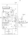
도 1은 입력 버퍼를 나타내는 회로도이다.
도 2는 도 1의 인버터부의 입출력 전압 특성을 도시하는 그래프이다.
도 3은 본 발명의 실시예에 의한 입력 버퍼를 나타내는 블록도이다.
도 4a는 도 3의 입력 버퍼에 구동 전압을 제공하는 주 바이어스 회로를 도시하는 도면이다.
도 4b는 가변 전압의 레벨에 따른 보조 전압들의 레벨의 일실시예를 도시하는 표이다.
도 4c는 도 2의 입력 버퍼에 구동 전압을 제공하는 보조 바이어스 회로를 도시하는 회로도이다.
도 5는 도 2의 입력 버퍼를 더 자세히 도시한 회로도이다.
도 6은 입력 신호가 로직 로우(Logic Low) 상태일 때의 입력 버퍼의 동작을 설명하기 위한 도면이다.
도 7은 도 5 및 6의 제 1 바이어스부의 일실시예를 도시하는 회로도이다.
도 8은 입력 신호가 로직 하이(Logic High) 상태일 때의 입력 버퍼의 동작을 설명하기 위한 도면이다.
도 9는 입력 신호가 고입력신호일때 입력 신호, 제 1 스테이지 및 제 2 스테이지의 입출력 전압 범위를 도시하는 도면이다.
도 10은 본 발명의 다른 실시예에 의한 입력 버퍼를 도시하는 회로도이다.1 is a circuit diagram showing an input buffer.
2 is a graph showing input / output voltage characteristics of the inverter unit of FIG.
3 is a block diagram illustrating an input buffer according to an embodiment of the present invention.
4A is a diagram showing a main bias circuit for providing a driving voltage to the input buffer of FIG. 3. FIG.
4B is a table showing one embodiment of the level of auxiliary voltages according to the level of the variable voltage.
4C is a circuit diagram illustrating an auxiliary bias circuit that provides a driving voltage to the input buffer of FIG.
5 is a circuit diagram showing the input buffer of FIG. 2 in more detail.
6 is a diagram for explaining the operation of the input buffer when the input signal is in a logic low state.
Fig. 7 is a circuit diagram showing one embodiment of the first bias portion in Figs. 5 and 6. Fig.
8 is a diagram for explaining the operation of the input buffer when the input signal is in a logic high state.
9 is a diagram showing input / output voltage ranges of the input signal, the first stage and the second stage when the input signal is a high input signal.
10 is a circuit diagram showing an input buffer according to another embodiment of the present invention.
이하, 본 발명이 속하는 기술 분야에서 통상의 지식을 가진 자가 본 발명의 기술적 사상을 용이하게 실시할 수 있도록 본 발명의 실시예가 첨부된 도면을 참조하여 설명한다. 또한 이하에서 사용되는 용어들은 오직 본 발명을 설명하기 위하여 사용된 것이며 본 발명의 범위를 한정하기 위해 사용된 것은 아니다. 앞의 일반적인 설명 및 다음의 상세한 설명은 모두 예시적인 것으로 이해되어야 하며, 청구된 발명의 부가적인 설명이 제공되는 것으로 여겨져야 한다.DETAILED DESCRIPTION OF THE PREFERRED EMBODIMENTS Hereinafter, embodiments of the present invention will be described with reference to the accompanying drawings so that those skilled in the art may easily implement the technical idea of the present invention. It is also to be understood that the terminology used herein is for the purpose of describing the present invention only and is not used to limit the scope of the present invention. It is to be understood that both the foregoing general description and the following detailed description are exemplary, and are intended to provide further explanation of the claimed invention.
본 발명에서 고입력신호는 로직 하이 상태에서 코어 전압(Vq) 및 저전원전압(Vp)보다 높은 전압, 예를 들어 3.3V가 입력되는 입력 신호를 의미한다. 저입력신호는 로직 하이 상태에서 저전원전압(Vp) 레벨의 전압, 예를 들어 1.8V가 입력되는 입력 신호를 의미한다.In the present invention, the high input signal means an input signal having a voltage higher than the core voltage Vq and the low power supply voltage Vp, for example, 3.3 V, in a logic high state. The low input signal means an input signal to which a voltage of a low power supply voltage (Vp) level, for example, 1.8 V, is input in a logic high state.
본 발명에서 저전압 반도체 장치는 저전원전압(Vp) 레벨의 전압에서 구동되는 반도체 장치를 의미한다. 상술된 바와 같이, 저전원전압(Vp)은 고입력신호의 로직 하이 상태 전압 레벨보다 낮은 전압 레벨이다. 예를 들어, 저전압 반도체 장치는 본 발명에서 중-게이트 산화층 반도체 장치일 수 있다.In the present invention, a low-voltage semiconductor device refers to a semiconductor device driven at a voltage of a low power supply voltage (Vp) level. As described above, the low power supply voltage Vp is a voltage level lower than the logic high state voltage level of the high input signal. For example, a low-voltage semiconductor device may be a medium-gate oxide semiconductor device in the present invention.
저전압 반도체 장치는 한계 전압을 가진다. 저전압 반도체 장치의 각 노드 간에 한계 전압 이상의 전압차가 발생되면, 저전압 반도체 장치는 파손되거나 이상 동작을 일으킬 수 있다.A low-voltage semiconductor device has a threshold voltage. If a voltage difference exceeding a threshold voltage is generated between nodes of the low-voltage semiconductor device, the low-voltage semiconductor device may be damaged or abnormal operation may occur.
도 1은 입력 버퍼를 나타내는 회로도이다. 도 1을 참조하면, 입력 버퍼(10)는 인버터부(11), 제 1 버퍼부(12) 및 제 2 버퍼부(13)를 포함한다. 인버터부(11)는 PMOS 트랜지스터들(Q2, Q3) 및 NMOS 트랜지스터들(Q1, Q4)을 포함한다. 인버터부(11)에 포함되는 트랜지스터들(Q1~Q4)은 저전압 반도체 장치들이다.1 is a circuit diagram showing an input buffer. Referring to FIG. 1, the
입력 버퍼(10)에 공급되는 바이어스 전압은 가변 전압(Vo), 저전원전압(Vp) 및 코어 전압(Vq)을 포함할 수 있다.The bias voltage supplied to the
저전원전압(Vp)은 트랜지스터들(Q1~Q4)에 규정된 한계 전압보다 낮은 전압 레벨의 전원 전압이다. 본 실시예에서 저전원전압(Vp)의 레벨은 약 1.8V라 가정한다.The low power supply voltage Vp is a power supply voltage at a voltage level lower than the threshold voltage defined by the transistors Q1 to Q4. In this embodiment, it is assumed that the level of the low power supply voltage Vp is about 1.8V.
가변 전압(Vo)은 입력 버퍼(10)로 제공되는 I/O 전압이다. 가변 전압(Vo)은 낮은 전압 레벨에서 높은 전압 레벨까지 다양한 레벨의 전압을 선택적으로 가질 수 있다. 예를 들어, 가변 전압(Vo)은 저전원전압(Vp)의 1, 1.5 혹은 2배의 크기의 전압 중 어느 하나를 선택적으로 가지도록 설정될 수 있다. 본 실시예에서 가변 전압(Vo)의 레벨은 1.8V, 2.5V 혹은 3.3V 중 어느 하나의 값을 가진다고 가정한다. 그러나 이는 예시적인 것으로, 입력 버퍼(10)의 특성(specification)에 따라 가변 전압(Vo)이 가질 수 있는 전압 레벨은 조절될 수 있을 것이다.The variable voltage Vo is the I / O voltage provided to the
코어 전압(Vq)는 입력 버퍼(10)와 연결될 전자 장치의 코어 전압이다. 코어 전압(Vq)은 전자 장치가 요구하는 동작 전압에 따라 결정될 수 있다.The core voltage Vq is the core voltage of the electronic device to be connected to the
입력 버퍼(10)의 트랜지스터들(Q1~Q4) 및 제 1 버퍼부(11)는 저전원전압(Vp)으로 구동된다. 이하 도면을 참조하여 입력 버퍼(10)의 동작 및 바이어싱(Biasing)에 관하여 설명한다.The transistors Q1 to Q4 and the
먼저, 입력 패드로 입력 신호(VIN)가 인가된다. 입력 신호(VIN)는 트랜지스터(Q2)의 게이트 및 트랜지스터(Q1)의 드레인으로 인가된다.First, the input signal VIN is applied to the input pad. The input signal VIN is applied to the gate of the transistor Q2 and the drain of the transistor Q1.
입력 신호(VIN)가 로직 로우 상태이면, 트랜지스터(Q2) 및 트랜지스터(Q3)가 턴 온 될 것이다. 트랜지스터들(Q2, Q3)이 턴 온 되면 인버터부(11)의 출력은 저전원전압(Vp) 레벨의 로직 하이 상태가 될 것이다. 저전원전압(Vp)은 트랜지스터들(Q1~Q4)에 규정된 한계 전압보다 낮은 전압 레벨을 가지므로, 트랜지스터들(Q1~Q4)는 파손되지 않고 안정적으로 구동될 것이다.When the input signal VIN is in a logic low state, the transistor Q2 and the transistor Q3 will be turned on. When the transistors Q2 and Q3 are turned on, the output of the
입력 신호(VIN)가 로직 하이 상태이면, 트랜지스터(Q1) 및 트랜지스터(Q4)가 턴 온 될 것이다. 트랜지스터들(Q1, Q4)이 턴 온 되면 인버터부(11)의 출력은 로직 로우 상태가 될 것이다. 입력 신호(VIN)의 레벨이 트랜지스터들(Q1~Q4)에 규정된 한계 전압보다 높은 전압 레벨을 가지는 경우에도, 트랜지스터(Q1)에 의하여, 트랜지스터(Q4)의 게이트에 인가되는 전압은 저전압신호(Vp)보다 낮은 레벨을 가지게 된다. 따라서 입력 신호(VIN)가 로직 하이 상태인 경우에도 트랜지스터들(Q1~Q4)는 파손되지 않고 안정적으로 구동될 것이다.When the input signal VIN is in the logic high state, the transistor Q1 and the transistor Q4 will be turned on. When the transistors Q1 and Q4 are turned on, the output of the
한편, 입력 버퍼(10)는 신뢰성있는 동작을 위하여 일정한 조건(specification)을 만족하여야 한다. 이하 도 2를 참조하여 입력 버퍼의 조건에 관하여 더 자세하게 설명한다.Meanwhile, the
도 2는 도 1의 인버터부(11)의 입출력 전압 특성을 도시하는 그래프이다. 도 2에서 가로축은 입력 신호(VIN)를, 세로축은 인버터부(110)의 출력단 전압을 나타낸다.2 is a graph showing input / output voltage characteristics of the
도 2를 참조하면, 입력 버퍼(10)의 인버터부(11)는 하한 로직 하이 입력 전압(Minimum Logic High Input Voltage, 이하 VIH) 및 상한 로직 로우 입력 전압(Maximum Logic Low Input Voltage, 이하 VIL)을 가진다. VIH는 인버터부(11)의 출력단이 로직 로우 상태일 것을 보장하는 최소 입력 신호 레벨이다. VIL은 인버터부(11)의 출력단이 로직 하이 상태일 것을 보장하는 최대 입력 신호 레벨이다. VIH 및 VIL은 도 2에서 도시된 바와 같이, 입출력 그래프의 기울기가 -1이 되는 지점에서의 입력 신호 레벨로 지정될 수 있다. 입력 신호의 레벨이 VIH와 VIL 사이이면 인버터부(11)의 출력은 불확정한 값이 될 것이다.Referring to FIG. 2, the
또한 인버터부(11)는 하한 로직 하이 출력 전압(Minimum Logic Ligh Output Voltage, 이하 VOH) 및 상한 로직 로우 출력 전압(Maximum Logic Low Output Voltage, 이하 VOL)을 가진다. VOH는 인버터부(11)의 출력단이 로직 하이 상태일 때 가질 수 있는 최소 전압 레벨이다. 즉, VOH는 입력 신호(VIN)가 VIL일 때의 출력 전압 레벨이 될 것이다. 반대로, VOL는 인버터부(11)의 출력단이 로직 로우상태일 때 가질 수 있는 최대 전압 레벨이다. 즉, VOL는 입력 신호(VIN)가 VIH일 때의 출력 전압 레벨이 될 것이다. VOH는 VIH보다 높은 레벨을 가진다. VOL은 VIL보다 낮은 레벨을 가진다.The
또한 인버터부(11)는 토글 전압(Toggle Voltage, 이하 Vtgl)을 가진다. 본 발명에서 Vtgl은 스위칭 포인트(switching point)와 동일한 의미로 사용된다. Vtgl은 인버터부(11)의 출력 전압 레벨이 로직 하이 상태 출력 레벨의 1/2일 때의 입력 전압이다.The
입력 버퍼(10)가 정상적으로 구동되기 위해서, 인버터부(11)는 수학식 1의 조건을 만족하여야 한다.In order for the

다시 도 1로 돌아가면, 도 1의 입력 버퍼(10)의 입력 신호가 고입력신호일 때, 입력 버퍼(10)의 인버터부(11)는 상술된 조건을 만족하기 어려워진다. 1, when the input signal of the
고입력신호가 로직 하이 상태일 때 이상적으로 VD, 예를 들어 3.3V, 레벨의 전압이 인가된다고 가정한다. 입력 신호에 포함되는 노이즈를 고려할 때, 인버터부(11)의 VIH는 0.7VD, VIL은 0.3VD 수준을 만족하여야 한다.It is assumed that a voltage of VD, for example, 3.3V, is applied ideally when the high input signal is in a logic high state. Considering the noise included in the input signal, VIH of the
수학식 1을 참조하면, 인버터부(11)의 Vtgl은 VIH와 VIL의 사이에 위치하여야 한다. 그러나, 인버터부(11)의 구동 전압은 저전원전압(Vp)이므로, 일반적인 경우 인버터부(11)의 vtgl은 1/2Vp가 되어 요구되는 VIL보다 낮아질 수 있다. vtgl이 요구되는 VIH 및 VIL 사이 구간에서 벗어남에 따라 입력 버퍼(10)의 신뢰성이 감소되고, 노이즈에 취약해 질 것이다.Referring to Equation (1), Vtgl of the
Vtgl을 VIH와 VIL 사이에 위치시키기 위하여 트랜지스터(Q4) 및 트랜지스터(Q2, Q3)의 종횡비(aspect ratio)가 조절될 수 있을 것이다. 그러나 토글 전압(Vtg)을 설정하기 위하여 트랜지스터(Q4)의 종횡비가 변화되면, 트랜지스터(Q2, Q3)와 트랜지스터(Q4) 사이의 동작 속도에 차이가 발생된다. 트랜지스터(Q2, Q3)와 트랜지스터(Q4)의 동작 속도가 불균형해짐에 따라 인버터부(10)의 스위칭 시간이 크게 제한될 수 있다. The aspect ratio of transistor Q4 and transistors Q2 and Q3 may be adjusted to place Vtgl between VIH and VIL. However, when the aspect ratio of the transistor Q4 is changed in order to set the toggle voltage Vtg, a difference occurs in the operation speed between the transistors Q2 and Q3 and the transistor Q4. As the operation speeds of the transistors Q2 and Q3 and the transistor Q4 become unbalanced, the switching time of the
따라서 본 발명에서는 입력 버퍼의 입력 신호로서 고입력신호가 사용되는 때에도 인버터부의 조건(specification)을 만족시키기 위하여, 가변 전압(Vo)을 구동 전압으로 사용하는 입력 버퍼를 제시한다. 또한 가변 전압(Vo)이 구동 전압으로 사용될 때 발생될 수 있는 입력 버퍼 내부 소자의 안정성 문제를 해결할 수 있는 입력 버퍼를 제시한다.Therefore, the present invention proposes an input buffer using a variable voltage Vo as a driving voltage in order to satisfy the specifications of the inverter unit even when a high input signal is used as an input signal of the input buffer. In addition, an input buffer capable of solving the stability problem of the internal elements of the input buffer which may be generated when the variable voltage Vo is used as the driving voltage is proposed.
도 3은 본 발명의 실시예에 의한 입력 버퍼(100)를 나타내는 블록도이다. 입력 버퍼(100)는 2개의 스테이지(stage)를 포함한다. 제 1 스테이지(stage 1)는 내부 소자들의 안정성을 확보하고, 또한 상술된 조건을 만족시키기 위하여 추가된 회로이다. 제 2 스테이지(stage 2)는 도 1에 도시된 입력 버퍼 회로이다.3 is a block diagram showing an
도 3의 입력 버퍼(100)는 가변 전압(Vo), 저전원전압(Vp) 및 코어 전압(Vq)을 구동 전압으로 사용한다. 가변 전압(Vo)은 복수의 미리 설정된 전압 레벨 중 하나의 값을 선택적으로 가질 것이다. 가변 전압(Vo)의 레벨은 입력 신호(VIN)의 로직 하이 상태 레벨에 응답하여 선택될 수 있다. 본 실시예에서 가변 전압(Vo)의 레벨은 Vp 내지 2Vp 범위에서 설정될 수 있다.The
본 실시예에서 저전원전압(Vp)은 1.8V로 설정된다. 또한 가변 전압(Vo)은 입력 신호(VIN)의 로직 하이 상태 레벨에 응답하여 1.8V, 2.5V 혹은 3.3V 중 하나의 값을 가지도록 설정된다. 그러나 이는 예시적인 것으로 본 발명의 저전원전압(Vp) 및 가변 전압(Vo)의 레벨이 이로 한정되는 것은 아니다.In this embodiment, the low power supply voltage Vp is set to 1.8V. The variable voltage Vo is also set to have one of 1.8V, 2.5V or 3.3V in response to the logic high state level of the input signal VIN. However, this is illustrative only and the level of the low power supply voltage Vp and the variable voltage Vo of the present invention is not limited thereto.
입력 버퍼(100)는 고입력신호가 입력되는 때에는 높은 레벨을 가지는 가변 전압(Vo)을 구동 전압으로 사용하여 특성(specification)을 만족시킬 수 있다. 또한 입력 버퍼(100)는 높은 레벨을 가지는 가변 전압(Vo)이 구동 전압으로 사용되어도 내부 소자들의 안정성 및 수명을 확보할 수 있도록 보조적인 회로 블록들을 구비한다. 입력 버퍼(100)의 구성 및 동작은 도 4a 내지 4c를 통해 더 자세히 설명될 것이다.When the high input signal is input, the
도 4a는 도 3의 입력 버퍼(100)에 구동 전압을 제공하는 주 바이어스 회로(101)를 도시하는 도면이다. 주 바이어스 회로(101)는 가변 전압(Vo), 저전원전압(Vp) 및 코어 전압(Vq)을 생성하여 입력 버퍼(100)로 제공한다. 또한 주 바이어스 회로는 제 1 보조 전압(Vo1), 제 2 보조 전압(Vo2) 및 제 3 보조 전압(Vo3)을 생성하여 입력 버퍼(100)로 제공한다.4A is a diagram showing a
제 1 보조 전압(Vo1), 제 2 보조 전압(Vo2) 및 제 3 보조 전압(Vo3)의 레벨은 가변 전압(Vo)의 레벨에 따라 가변된다. 보조 전압들(Vo1~Vo3)은 복수 레벨의 가변 전압(Vo) 중 어떤 레벨의 전압이 인가되어도 입력 버퍼(100)의 내부 소자들이 안정성을 유지할 수 있도록, 입력 버퍼(100)의 각 부분에 조절된 바이어스 전압을 제공할 것이다.The levels of the first auxiliary voltage Vo1, the second auxiliary voltage Vo2 and the third auxiliary voltage Vo3 vary according to the level of the variable voltage Vo. The auxiliary voltages Vo1 to Vo3 are controlled by adjusting the respective portions of the
도 4b는 가변 전압(Vo)의 레벨에 따른 보조 전압들(Vo1~Vo3)의 레벨의 일실시예를 도시하는 표이다. 도 4b를 참조하면, 가변 전압(Vo)이 변화됨에 따라 보조 전압들(Vo1~Vo3)의 레벨도 가변된다. 보조 전압들(Vo1~Vo3)에 의하여 바이어스되는 입력 버퍼(100)의 동작은 이후 도 5를 참조하여 더 자세히 설명될 것이다.4B is a table showing one embodiment of levels of the auxiliary voltages Vo1 to Vo3 according to the level of the variable voltage Vo. Referring to FIG. 4B, as the variable voltage Vo changes, the level of the auxiliary voltages Vo1 to Vo3 also varies. The operation of the
도 4c는 도 2의 입력 버퍼(100)에 구동 전압을 제공하는 보조 바이어스 회로(102)를 도시하는 회로도이다. 보조 바이어스 회로(102)는 도 3B의 주 바이어스 회로로부터 제 2 및 제 3 보조 전압(Vo2, Vo3)을 입력받는다. 보조 바이어스 회로(102)는 입력된 제 2 및 제 3 보조 전압(Vo2, Vo3)을 부정 논리곱(NAND)하여 제 4 보조 전압(Vo4)을 생성한다. 또, 보조 바이어스 회로(102)는 입력된 제 3 보조 전압(Vo3)을 반전하여 제 5 보조 전압(Vo5)을 생성한다. 보조 전압들(Vo4~Vo5)에 의하여 구동되는 입력 버퍼(100)의 동작은 이후 도 5를 참조하여 더 자세히 설명될 것이다.4C is a circuit diagram showing an
도 5는 도 2의 입력 버퍼(100)를 더 자세히 도시한 회로도이다. 도 5를 참조하면, 입력 버퍼(100)는 제 1 스테이지(stage 1) 및 제 2 스테이지(stage 2)를 포함한다. 제 1 스테이지(stage 1)에 포함되는 PMOS 트랜지스터들의 각 노드들에는, 입력 신호의 상태에 따라 고전압이 인가될 수 있다. 따라서 웰 누설 전류(well leakage current)를 방지하기 위하여, 제 1 스테이지(stage 1)에 포함되는 PMOS 트랜지스터들의 웰 바이어스(well bias) 전압으로서 가변 전압(Vo)이 인가된다.5 is a circuit diagram showing the
상술된 바와 같이, 가변 전압(Vo)은 복수 레벨의 전압 중 하나의 값을 선택적으로 가질 수 있다. 본 발명에서 가변 전압(Vo)의 레벨은 입력 신호가 로직 하이상태일 때의 전압 레벨에 기초하여 설정된다. 입력 신호가 고입력신호인 경우, 가변 전압(Vo)은 높은 레벨, 예를 들어 3.3V,로 설정될 수 있을 것이다. 입력 신호가 저입력신호인 경우, 가변 전압(Vo) 역시 낮은 레벨, 예를 들어 1.8V, 로 설정될 수 있을 것이다.As described above, the variable voltage Vo may have a value of one of several levels of voltage. In the present invention, the level of the variable voltage Vo is set based on the voltage level when the input signal is in the logic high state. When the input signal is a high input signal, the variable voltage Vo may be set to a high level, for example, 3.3V. When the input signal is a low input signal, the variable voltage Vo may also be set to a low level, for example, 1.8V.
도 5를 참조하면, 입력 버퍼(100)의 제 1 스테이지(stage 1)는 풀업부(110), 풀다운부(120), 풀업 제어부(130), 제 1 풀업 보호부(140), 제 1 바이어스부(150), 제 2 풀업 보호부(160), 제 3 풀업 보호부(170), 풀다운 제어부(180) 및 제 2 바이어스부(190)를 포함한다.5, the
본 발명의 입력 버퍼(100)는 고입력신호가 입력 신호로서 인가되는 경우, 가변 전압(Vo)을 높은 레벨로 설정한다. 입력 버퍼(100)는 높은 레벨로 설정된 가변 전압(Vo)을 풀업부(110)의 동작 전압으로 사용한다. 가변 전압(Vo)이 풀업부(110)의 동작 전압으로 사용됨에 따라, 입력 버퍼(100)의 인버터단, 즉 풀업부(110) 및 풀다운부(120)의 vtgl은 1/2Vo 레벨에 위치하게 된다. 따라서 입력 버퍼(100)는 고입력신호가 인가되는 경우에도 상술된 특성(specification)을 만족시킬 수 있다.The
높은 레벨로 설정된 가변 전압(Vo)이 풀업부(110)의 동작 전압으로 사용될 때, 고입력신호가 로직 로우 상태인 경우 풀업부(110)의 게이트-소스 간의 전압 차는 풀업부(110)에 포함된 트랜지스터의 규정된 한계 전압보다 커질 수 있다. 입력 버퍼(100)는 풀업부(110)를 보호하기 위하여, 로직 로우 상태인 입력 신호를 풀업부(110)의 게이트에 직접(directly) 전달하지 않는다. 대신, 입력 버퍼(110)는 제 1 바이어스부(150) 및 제 1 풀업 보호부(140)를 이용하여 풀업부(110)에 풀업부(110)를 턴 온 시킬 정도의 낮은 전압을 제공한다. 그러나 상기 제공된 전압은 풀업부(110)의 게이트-드레인 간 전압 차이를 풀업부(110)가 저항할 수 있는 정도로는 높은 전압이다. 따라서 입력 버퍼(100)는 고입력신호가 로직 로우 상태인 경우에도 안정성 및 수명을 확보할 수 있다.When the high input signal is in a logic low state, the voltage difference between the gate and the source of the pull-up
이하 도 6 내지 8을 참조하여 제 1 스테이지(stage 1)의 동작을 더 자세히 설명한다.The operation of the first stage (stage 1) will now be described in more detail with reference to FIGS. 6-8.
도 6은 입력 신호가 로직 로우(Logic Low) 상태일 때의 입력 버퍼(100)의 동작을 설명하기 위한 도면이다.6 is a diagram for explaining the operation of the
1. 입력 신호가 고입력신호인 경우1. When the input signal is high input signal
입력 신호가 고입력신호이면, 고입력신호에 대응하여 가변 전압(Vo)은 높은 레벨, 예를 들어 3.3V로 설정된다.If the input signal is a high input signal, the variable voltage Vo is set to a high level, for example, 3.3 V, corresponding to the high input signal.
입력 신호가 로직 로우(Logic Low) 상태이면, 게이트가 입력 신호와 타이(tie)된 트랜지스터(P2)가 턴 온 된다. 트랜지스터(P1)는 턴 오프 된다. 트랜지스터(P2)가 턴 온 됨에 따라, 노드(A)의 레벨은 입력 신호보다 약간 높은 레벨(VIN+Vtp2)로 증가된다. Vtp2는 PMOS 트랜지스터(P2)의 문턱 전압이다.When the input signal is in a logic low state, the transistor P2 whose gate is tied with the input signal is turned on. The transistor P1 is turned off. As the transistor P2 is turned on, the level of the node A is increased to a level (VIN + Vtp2) slightly higher than the input signal. Vtp2 is the threshold voltage of the PMOS transistor P2.
한편, 제 1 바이어스부(150)는 가변 전압(Vo)의 레벨에 따라 선택적으로 미리 지정된 전압 레벨들 중 하나의 레벨의 전압을 제공한다. 예를 들어, 제 1 바이어스부(150)는 저전원전압(Vp), 코어전압(Vq) 및 접지 전압 중 하나의 전압을 선택적으로 트랜지스터(P4)의 드레인에 제공한다.On the other hand, the
도 7은 도 5 및 도 6의 제 1 바이어스부(150)의 일실시예를 도시하는 회로도이다. 도 7을 참조하면, 제 1 바이어스부(150)는 전압 선택을 위한 트랜지스터들(P12, P13, N16)을 포함한다.FIG. 7 is a circuit diagram showing one embodiment of the
트랜지스터들(P12, P13, N16)은 보조 전압들(Vo2, Vo4, Vo5)에 의하여 선택적으로 턴 온 된다. 도 2 및 도 3에 설명된 보조 전압들(Vo2, Vo4, Vo5)을 참조하면, 트랜지스터들(P12, P13, N16)은 가변 전압(Vo)의 레벨에 따라 선택적으로 턴 온 될 것이다.The transistors P12, P13 and N16 are selectively turned on by the auxiliary voltages Vo2, Vo4 and Vo5. Referring to the auxiliary voltages Vo2, Vo4 and Vo5 described in FIGS. 2 and 3, the transistors P12, P13 and N16 will be selectively turned on according to the level of the variable voltage Vo.
예를 들어, 가변 전압(Vo)이 높은 전압, 즉 3.3V이면, 트랜지스터(P12)만 턴 온 된다. 트랜지스터(P12)가 턴 온 되면 트랜지스터(P4)의 드레인에 저전원전압(Vp)이 제공된다. 마찬가지로, 가변 전압(Vo)이 중간 전압, 즉 2.5V이면, 트랜지스터(P13)만 턴 온 된다. 트랜지스터(P13)가 턴 온 되면 트랜지스터(P4)의 드레인에 코어전압(Vq)이 제공된다. 가변 전압(Vo)이 낮은 전압, 즉 1.8V이면, 트랜지스터(N16)만 턴 온 된다. 트랜지스터(N16)가 턴 온 되면 트랜지스터(P4)의 드레인에는 접지 전압이 제공된다.For example, when the variable voltage Vo is a high voltage, that is, 3.3 V, only the transistor P12 is turned on. When the transistor P12 is turned on, the drain of the transistor P4 is supplied with the low power supply voltage Vp. Similarly, when the variable voltage Vo is an intermediate voltage, that is, 2.5 V, only the transistor P13 is turned on. When the transistor P13 is turned on, the core voltage Vq is supplied to the drain of the transistor P4. When the variable voltage Vo is a low voltage, that is, 1.8 V, only the transistor N16 is turned on. When the transistor N16 is turned on, the drain of the transistor P4 is provided with the ground voltage.
상술된 제 1 바이어스부(150)는 가변 전압(Vo)의 레벨에 따라 선택적으로 저전원전압(Vp), 코어전압(Vq) 및 접지 전압 중 하나의 전압을 트랜지스터(P4)의 드레인에 제공하는 역할을 한다. 도 7에 도시된 제 1 바이어스부(150)는 예시적인 것으로, 본 발명의 제 1 바이어스부가 이에 한정되는 것은 아니다. 예를 들어, 제 1 바이어스부는 가변 전압(Vo)의 레벨에 응답하여 선택된 레벨의 전압을 제공하는 외부 바이어스 회로일 수 있다.The
다시 도 6으로 돌아가면, 게이트가 노드(SP)와 연결된 트랜지스터(N4)는 노드(B)의 전압을 (노드(SP)의 전압 - Vtn4)이 되도록 한다. Vtn4는 NMOS 트랜지스터(N4)의 문턱 전압이다. 정리하면, 제 1 풀업 보호부(140)는, 입력 신호가 로직 로우 상태일 때, 풀업 제어부(130)의 제어에 응답하여 노드(B)의 전압이 (노드(SP)의 전압 - Vtn)이 되도록 한다.6, the transistor N4 whose gate is connected to the node SP makes the voltage of the node B (the voltage of the node SP - Vtn4). Vtn4 is the threshold voltage of the NMOS transistor N4. In summary, when the input signal is in a logic low state, the first pull-up
풀업부(110)에서, 트랜지스터(P6)의 게이트는 노드(B)와 연결되므로 트랜지스터(P6)는 턴 온 된다. 트랜지스터(P6)가 턴 온 됨에 따라 노드(E)의 전압은 가변 전압(Vo) 레벨로 상승될 것이다.In the pull-up
트랜지스터(P6)의 드레인에 공급되는 가변 전압(Vo)은 트랜지스터(P6)에 규정된 한계 전압보다 높은 전압일 수 있다. 그러나 상술된 바와 같이, 노드(B)의 전압은, 제 1 풀업 보호부(140)에 의하여, 접지 전압보다 높은 (노드(SP)의 전압 - Vtn)으로 상승된다.The variable voltage Vo supplied to the drain of the transistor P6 may be a voltage higher than the limit voltage specified for the transistor P6. However, as described above, the voltage of the node B is raised by the first pull-up
노드(B)의 전압은 트랜지스터(P6)를 턴 온 시킬 정도의 낮은 전압이다. 그러나 노드(B)의 전압은 트랜지스터(P6)의 게이트-드레인 간 전압 차이를 트랜지스터(P6)가 저항할 수 있는 정도로는 높은 전압이다. 따라서 트랜지스터(P6)는 드레인에 높은 전압이 공급되어도 안정성 및 수명을 확보할 수 있다.The voltage of the node B is low enough to turn on the transistor P6. However, the voltage of the node B is high enough to allow the transistor P6 to resist the gate-drain voltage difference of the transistor P6. Therefore, even if a high voltage is supplied to the drain of the transistor P6, stability and lifetime can be ensured.
정리하면, 제 1 풀업 보호부(140) 및 제 1 바이어스부(150)는 입력 신호로서 고입력신호가 입력될 때, 입력 신호가 로우 레벨일 때에도 풀업부(110)의 소자의 안정성에 문제가 생기지 않도록 풀업부(110)를 보호한다. 제 1 풀업 보호부(140) 및 제 1 바이어스부(150)는 로우 레벨 신호를 그대로 풀업부(110)에 인가하는 것이 아니라 (노드(SP)의 전압 - Vtn) 레벨로 상승된 전압을 인가하여 풀업부(110)를 보호한다.In summary, when the high input signal is inputted as the input signal, the first pull-up
또, 제 2 풀업 보호부(160)에서, 트랜지스터(P6)가 턴 온 되면, 트랜지스터(P7)의 게이트는 제 1 보조 전압(Vo1)을 입력받으므로 트랜지스터(P7)는 턴 온 된다. 제 1 보조 전압(Vo1)은 트랜지스터(P7)를 턴 온 시킬 정도의 낮은 전압이다. 그러나 제 1 보조 전압(Vo1)은 트랜지스터(P7)의 게이트-드레인 간 전압 차이를 트랜지스터(P7)가 저항할 수 있는 정도로는 높은 전압이다. 따라서 트랜지스터(P7)는 드레인에 높은 전압, 즉 가변 전압(Vo)이 공급되어도 안정성 및 수명을 확보할 수 있다. 트랜지스터(P7)가 턴 온 됨에 따라 노드(F)의 전압은 가변 전압(Vo) 레벨로 상승될 것이다. 제 2 풀업 보호부(160)의 역할은 도 7을 참조하여 더 자세히 설명될 것이다.In the second pull-up
한편, 노드(F)의 전압이 가변 전압(Vo) 레벨로 상승되어도 풀 다운부(120)의 트랜지스터(N5)가 턴 온 되어 고전압을 차단하므로 트랜지스터(N6)의 안정성은 유지될 것이다.On the other hand, even if the voltage of the node F rises to the variable voltage Vo level, the transistor N5 of the pull-down
이때, 트랜지스터(N3)은 턴 오프 되어 노드(A)와 노드(B)가 연결되지 않도록 한다. 그러나, 트랜지스터(P2)에 의하여 노드(A)는 접지 레벨 보다 조금 높은 전압을 가지므로, 트랜지스터(N3)는 부분적으로 턴 온 될 수 있다. 트랜지스터(N3)가 턴 온 되면 노드(B)로부터 노드(A) 및 입력 패드로 누설 전류가 흐를 수 있다.At this time, the transistor N3 is turned off so that the node A and the node B are not connected. However, since the node A has a voltage slightly higher than the ground level by the transistor P2, the transistor N3 can be partially turned on. When the transistor N3 is turned on, a leakage current may flow from the node B to the node A and the input pad.
풀업 제어부(130)는, 트랜지스터(N3)의 턴 온 동작을 방지하기 위하여, 트랜지스터(N17)를 포함한다. 트랜지스터(N17)의 게이트는 제 2 바이어스 회로(190)로부터 방전 신호(NLC)를 제공받는다. 방전 신호(NLC)는 입력 신호(VIN)가 로직 로우 상태이면 저전원전압(Vp), 로직 하이 상태이면 접지 레벨을 가진다. The pull-up
입력 신호(VIN)가 로직 로우 상태이면, 트랜지스터(N17)는 방전 신호(NLC)에 응답하여 턴 온 된다. 턴 온된 트랜지스터(N17)는 트랜지스터(N3)의 게이트를 풀 다운 하여 트랜지스터(N3)가 완전히 턴 오프 되도록 한다. 트랜지스터(N17)는 입력 신호(VIN)가 로직 하이 상태이면 턴 오프 되므로, 입력 신호(VIN)의 로직 로우 및 로직 하이 상태 양쪽에서 누설 전류가 차단될 수 있다.When the input signal VIN is in a logic low state, the transistor N17 is turned on in response to the discharge signal NLC. The turned-on transistor N17 pulls down the gate of the transistor N3 so that the transistor N3 is completely turned off. The transistor N17 is turned off when the input signal VIN is in the logic high state, so that the leakage current can be cut off in both the logic low and logic high states of the input signal VIN.
상술된 바와 같이, 본 발명의 제 1 스테이지(stage 1)는 입력 신호가 고입력신호 혹은 중입력신호인 경우, 입력 신호가 로직 로우 상태일때 로직 하이 상태의 출력 전압을 안정성 및 신뢰성의 문제 없이 출력단, 즉 노드(F)에 제공할 수 있다. 또한 본 발명의 제 1 스테이지(stage 1)는 방전 회로를 구비하여 누설 전류를 차단할 수 있다.As described above, the first stage (stage 1) of the present invention is configured so that when the input signal is a high input signal or a medium input signal, the output voltage in a logic high state when the input signal is in a logic low state, , That is, to the node F. Also, the first stage (stage 1) of the present invention may include a discharge circuit to block leakage current.
2. 입력 신호가 저입력신호인 경우2. If the input signal is low input signal
입력 신호(VIN)가 저입력신호이면, 저입력신호에 대응하여 가변 전압(Vo)은 낮은 레벨, 예를 들어 1.8V로 설정된다.If the input signal VIN is a low input signal, the variable voltage Vo is set to a low level, for example, 1.8 V, corresponding to the low input signal.
입력 신호(VIN)가 저입력신호일 때 제 3 풀업 보호부(170)의 트랜지스터(N14)는 턴 온 된다. 트랜지스터(N14)가 턴 온 되면 제 3 풀업 보호부(170)의 트랜지스터들(N13~N15)는 모두 턴 온 되고, 입력 신호(VIN)는 노드(B)로 전달된다.When the input signal VIN is a low input signal, the transistor N14 of the third pull-up
풀업부(110)의 동작 전압은 낮은 레벨의 가변 전압(Vo)이므로, 풀업부(110)는 안정성 및 신뢰성의 문제 없이 노드(F)에 로직 하이 레벨의 출력 전압을 제공할 것이다. 트랜지스터(N14)는 입력신호(VIN)가 고입력신호 및 중입력신호인 때는 턴 오프 되므로, 입력신호(VIN)가 저입력신호가 아닌 경우에는 입력 신호(VIN)가 직접 풀업부(110)로 인가되는 제 3 풀업 보호부(170)는 차단될 것이다.Up
상술된 바와 같이, 본 발명의 제 1 스테이지(stage 1)는 입력 신호가 저입력신호인 경우에도, 입력 신호가 로직 로우 상태일때 로직 하이 상태의 출력 전압을 안정성 및 신뢰성의 문제 없이 출력단, 즉 노드(F)에 제공할 수 있다. As described above, the first stage (stage 1) of the present invention allows the output voltage of the logic high state to be output to the output stage, that is, the node (node), without a problem of stability and reliability, even when the input signal is a low input signal, (F).
도 8은 입력 신호가 로직 하이(Logic High) 상태일 때의 입력 버퍼(100)의 동작을 설명하기 위한 도면이다. 입력 신호(VIN)가 로직 로우(Logic low) 상태에서 로직 하이(Logic High) 상태로 변화되면, 풀다운 제어부(180)의 트랜지스터(N1)는 턴 온 된다. 트랜지스터(N1)는 높은 레벨의 입력 신호(VIN)가 직접 풀다운부(120)로 전달되는 것을 방지한다. 트랜지스터(N1)가 턴 온 됨에 따라 노드(C)의 전압은 저전원전압(Vp)-Vtn1 레벨까지 증가된다. Vtnl은 트랜지스터(N1)의 문턱 전압이다.8 is a diagram for explaining the operation of the
노드(C)의 전압이 증가되면, 풀다운부(120)의 트랜지스터(N6)는 턴 온 된다.트랜지스터(N6)가 턴온 되면, 저전원전압(Vp)이 게이트에 공급되는 트랜지스터(N5)도 턴 온 된다. 트랜지스터들(N5, N6)이 턴 온 됨에 따라, 노드(F)의 레벨은 접지 전압 레벨로 감소된다.When the voltage of the node C is increased, the transistor N6 of the pull-down
한편, 입력 신호(VIN)가 로직 로우(Logic low) 상태에서 로직 하이(Logic High) 상태로 변화되면, 트랜지스터(P1)가 턴 온 된다.On the other hand, when the input signal VIN changes from a logic low state to a logic high state, the transistor P1 is turned on.
트랜지스터(P1)가 턴 온 됨에 따라 노드(A)의 전압은 입력 신호(VIN) 레벨로 증가된다. 노드(A)의 전압 레벨이 증가됨에 따라 노드(A)와 게이트가 연결된 트랜지스터(P4)는 턴 오프 되므로, 노드(B)에는 제 1 바이어스부(150)에서 생성된 바이어스 전압이 공급되지 않는다.As the transistor P1 is turned on, the voltage of the node A is increased to the input signal VIN level. The bias voltage generated in the
또한 노드(A)의 전압 레벨이 증가됨에 따라 트랜지스터(N3)의 게이트에 입력 신호(VIN) 레벨의 고전압이 인가되는 것을 방지하기 위하여, 트랜지스터(N2)가 턴 온 된다. 트랜지스터(N2)는 트랜지스터(N3)의 게이트에 저전원전압(Vp)-Vtn2 레벨의 전압이 인가되게 한다. Vtn2는 트랜지스터(N2)의 문턱 전압이다.Further, the transistor N2 is turned on to prevent the high voltage of the input signal VIN level from being applied to the gate of the transistor N3 as the voltage level of the node A increases. The transistor N2 applies a voltage of the low power supply voltage (Vp) -Vtn2 level to the gate of the transistor N3. Vtn2 is the threshold voltage of the transistor N2.
한편, 입력 신호(VIN)가 로직 하이 상태이면, 게이트가 제 1 보조 전압(Vo1)과 연결된 트랜지스터(P3)는 턴 온 된다. 트랜지스터(P3)가 턴 온 됨에 따라 노드(B)의 전압은 입력 신호(VIN) 레벨로 증가된다. 노드(B)의 전압이 증가되면, 풀업부(110)의 트랜지스터(P6)는 턴 오프 된다. 트랜지스터(P6)의 드레인에는 높은 레벨의 가변 전압(Vo)이 제공된다. 따라서 트랜지스터(P6)는 게이트에 입력 신호(VIN) 레벨의 고전압이 인가되어도, 안정성 및 수명을 확보할 수 있다.On the other hand, when the input signal VIN is in a logic high state, the transistor P3 whose gate is connected to the first auxiliary voltage Vo1 is turned on. As the transistor P3 is turned on, the voltage of the node B is increased to the input signal VIN level. When the voltage of the node B is increased, the transistor P6 of the pull-up
또한 풀업부(110)를 보호하기 위하여, 제 2 풀업 보호부(160)의 트랜지스터(P7)가 턴 온 된다. 트랜지스터(P7)가 턴 온 됨에 따라 노드(E)의 전압은 접지 전압보다 높은 제 1 바이어스 전압(Vo1) + Vtp7 레벨로 증가된다. Vtp7은 트랜지스터(P7)의 문턱 전압이다. 노드(E)에 접지 레벨보다 높은 전압이 인가되므로, 게이트에 높은 레벨의 입력 신호(VIN)가 인가되어도 트랜지스터(P6)의 안정성 및 수명이 확보될 수 있다.In order to protect the pull-up
상술된 바와 같이, 본 발명의 제 1 스테이지(stage 1)는 입력 신호가 고입력신호인 경우에도, 입력 신호가 로직 하이 상태일때 로직 로우 상태의 출력 전압을 안정성 및 신뢰성의 문제 없이 출력단, 즉 노드(F)에 제공할 수 있다.As described above, the first stage (stage 1) of the present invention allows the output voltage of the logic low state to be outputted to the output stage, that is, the node (node), without a problem of stability and reliability when the input signal is in the logic high state, (F).
상술된 바와 같이, 도 6 내지 8을 참조하면, 입력 버퍼(100)의 제 1 스테이지(stage 1)는 어떤 입력 신호에 대하여도 출력 전압을 안정성 및 신뢰성의 문제 없이 출력단, 즉 노드(F)에 제공할 수 있다.6 through 8, the first stage (stage 1) of the
입력 버퍼(100)의 제 2 스테이지(stage 2)는 제 1 스테이지의 출력단, 즉 노드(F)의 전압을 입력 신호로서 제공받는다. 도 1에서 설명된 바와 같이, 제 2 스테이지(stage 2)는 저전원전압(Vp)으로 동작된다. 도 1에서 설명된 바와 같이, 제 2 스테이지(stage 2)는 높은 레벨의 입력 신호가 입력되어도, 트랜지스터(N8)가 턴 온 되어 낮은 전압을 제공하므로 안정적으로 동작할 수 있다. 이하 도 9를 참조하여 제 1 스테이지(stage 1) 및 제 2 스테이지(stage 2)의 전체 동작에 관련하여 설명한다.The second stage (stage 2) of the
도 9는 입력 신호가 고입력신호일때 입력 신호, 제 1 스테이지 및 제 2 스테이지의 입출력 전압 범위를 도시하는 도면이다.9 is a diagram showing input / output voltage ranges of the input signal, the first stage and the second stage when the input signal is a high input signal.
도 9를 참조하면, 입력 신호(VIN)는 로직 하이 상태일때 높은 전압(VD) 레벨, 예를 들어 3.3V, 을 가진다. 한편, 제 1 스테이지(stage 1)은 고입력신호가 입력될 때 높은 레벨, 예를 들어 VD,의 가변 전압으로 동작된다.Referring to FIG. 9, the input signal VIN has a high voltage (VD) level, for example, 3.3 V, when in a logic high state. On the other hand, the first stage (stage 1) is operated at a high level, for example, a variable voltage of VD, when a high input signal is input.
회로의 신뢰성을 위하여, 입력 버퍼(100)의 하한 로직 하이 입력 전압(이하 VIH) 및 상한 로직 로우 입력 전압(VIL)은 0.7VD 및 0.3VD 레벨 수준을 만족하여야 한다. 본 실시예에서, 제 1 스테이지(stage 1)의 동작 전압은 높은 레벨을 가지므로, 제 1 스테이지(stage 1)의 토글 전압(Vtgl)은 VIH 및 VIL 사이에 위치할 수 있다.For reliability of the circuit, the lower logic high input voltage (VIH) and the upper logic low input voltage (VIL) of the
제 1 스테이지(stage 1)는 입력 패드에 로직 로우 상태의 신호가 입력되면, 로직 하이 상태의 신호를 출력한다. 제 1 스테이지(stage 1)가 출력하는 로직 하이 상태의 신호는 하한 로직 하이 출력 전압(이하 VOH1) 이상의 값을 가진다. 제 1 스테이지(stage 1)는 입력 패드에 로직 하이 상태의 신호가 입력되면, 로직 로우 상태의 신호를 출력한다. 제 1 스테이지(stage 1)가 출력하는 로직 로우 상태의 신호는 상한 로직 로우 출력 전압(이하 VOL1) 이하의 값을 가진다.The first stage (stage 1) outputs a signal of logic high state when a signal of logic low state is inputted to the input pad. The signal of the logic high state output by the first stage (stage 1) has a value equal to or higher than the lower limit logic high output voltage (VOH1). The first stage (stage 1) outputs a logic low state signal when a logic high state signal is input to the input pad. The signal in the logic low state output by the first stage (stage 1) has a value below the upper limit logic low output voltage (VOL1).
제 2 스테이지(stage 2)는 저전원전압(Vp)으로 동작된다. 제 2 스테이지(stage 2)의 토글 전압(이하 Vtgl2)은 0.5Vp 레벨을 가질 것이다. The second stage (stage 2) is operated with the low power supply voltage Vp. The toggle voltage (hereinafter referred to as Vtgl2) of the second stage (stage 2) will have a level of 0.5 Vp.
제 1 스테이지(stage 1)가 로직 하이 상태의 신호를 출력할 때, 제 2 스테이지(stage 2)는 트랜지스터(도 5 내지 도 7 참조, N8)를 이용하여 저전원전압(Vp)보다 낮은 레벨의 전압을 풀다운부(도 5 내지 도 7 참조, N12)에 전달한다. 따라서 제 2 스테이지(stage 2)는 높은 레벨의 입력 신호가 입력되어도 안정적으로 동작할 수 있다.When the first stage (stage 1) outputs a signal of a logic high state, the second stage (stage 2) uses a transistor (N8 in Fig. 5 to Fig. 7) And transmits the voltage to the pull-down section (see Figs. 5 to 7, N12). Accordingly, the second stage (stage 2) can stably operate even when a high level input signal is input.
한편, 상술된 바와 같이, 제 1 스테이지(stage 1)가 로직 로우 상태의 신호를 출력할 때, 제 1 스테이지(stage 1)가 출력하는 로직 로우 상태의 신호는 VOL1 이하의 값을 가진다. 도시된 바와 같이 VOL1은 제 2 스테이지(stage 2)의 토글 전압(Vtgl2)보다 낮은 값을 가지므로, 제 2 스테이지(stage 2)는 제 1 스테이지(stage 1)로부터 로직 로우 상태의 신호가 입력되어도 신뢰성 있게 동작할 수 있다.On the other hand, as described above, when the first stage (stage 1) outputs a signal of a logic low state, the signal of the logic low state output by the first stage (stage 1) has a value of VOL1 or less. As shown, VOL1 has a value lower than the toggle voltage Vtgl2 of the second stage (stage 2), so that the second stage (stage 2) can receive the signal from the first stage (stage 1) It can operate reliably.
또한 도시된 바와 같이 입력 버퍼(100) 전체의 토글 전압(이하 Vtgl)은 0.5VD와 0.5Vp 사이에 위치하게 된다. 따라서 입력 버퍼(100)의 Vtgl은 입력 버퍼의 VIH 및 VIL 사이에 위치할 수 있다.Also, as shown in the figure, the toggle voltage (hereinafter referred to as Vtgl) of the
상술한 저전압 소자 입력 버퍼(100)는 제 1 스테이지(stage 1) 및 제 2 스테이지(stage)를 이용하여, 고입력신호가 입력되는 때에도 안정성 및 신뢰성의 문제 없이 동작할 수 있다.The low-
도 10은 본 발명의 다른 실시예에 의한 입력 버퍼(200)를 도시하는 회로도이다. 도 10을 참조하면, 도 10의 입력 버퍼(200)는 풀업부(210), 풀다운부(220), 풀업 제어부(230), 제 1 풀업 보호부(240), 제 1 바이어스부(250), 제 2 풀업 보호부(260), 제 3 풀업 보호부(270), 풀다운 제어부(280), 제 2 바이어스부(290), 낮은 문턱 전압 조절부(Low Threshold Voltage Modulating Unit, 310) 및 높은 문턱 전압 조절부(High Threshold Voltage Modulating Unit, 320)를 포함한다.10 is a circuit diagram showing an
도 10의 입력 버퍼(200)의 풀업 제어부(230), 제 1 풀업 보호부(240), 제 1 바이어스부(250), 제 2 풀업 보호부(260), 제 3 풀업 보호부(270), 풀다운 제어부(280) 및 제 2 바이어스부(290)는 도 1의 풀업 제어부(130), 제 1 풀업 보호부(140), 제 1 바이어스부(150), 제 2 풀업 보호부(160), 제 3 풀업 보호부(170), 풀다운 제어부(180) 및 제 2 바이어스부(190)과 그 구성 및 동작이 동일하다. 따라서 풀업부(210), 풀다운부(220), 낮은 문턱 전압 조절부(Low Threshold Voltage Modulating Unit, 310) 및 높은 문턱 전압 조절부(High Threshold Voltage Modulating Unit, 320)에 관하여만 자세히 설명한다.Up
입력 버퍼(200)는 낮은 문턱 전압 조절부(310) 및 높은 문턱 전압 조절부(320)를 이용하여 슈미트 트리거 회로(Schmitt Trigger Circuit)와 같이 동작한다. 입력 버퍼(200)는 낮은 문턱 전압(Low Threshold Voltage, 이하 Vspl) 및 높은 문턱 전압(High Threshold Voltage, 이하 Vsph)을 조절하여 노이즈 마진을 증가시킬 수 있다.The
본 발명에서 Vspl 및 Vsph는 제 1 스테이지(stage 1)의 문턱 전압이다. 제 1 스테이지(stage 1)의 출력단, 즉 노드(F)가 로직 로우 상태일 때, 노드(F)는 입력 신호(VIN)의 전압 레벨이 Vsph에 도달할 때 까지 로직 로우 상태의 전압을 유지할 것이다. 노드(F)는 입력 신호(VIN)의 전압 레벨이 Vsph 이상이 되면 로직 하이 상태로 전환될 것이다.In the present invention, Vspl and Vsph are the threshold voltages of the first stage (stage 1). When the output stage of the first stage (stage 1), i.e. node F, is in a logic low state, node F will maintain a voltage of logic low state until the voltage level of input signal VIN reaches Vsph . The node F will transition to a logic high state when the voltage level of the input signal VIN is greater than Vsph.
또한 제 1 스테이지(stage 1)의 출력단, 즉 노드(F)가 로직 하이 상태일 때, 노드(F)는 입력 신호(VIN)의 전압 레벨이 Vspl에 도달할 때 까지 로직 하이 상태의 전압을 유지할 것이다. 노드(F)는 입력 신호(VIN)의 전압 레벨이 Vspl 이하가 되면 로직 로우 상태로 전환될 것이다.Further, when the output stage of the first stage (stage 1), that is, when the node F is in the logic high state, the node F maintains the voltage of the logic high state until the voltage level of the input signal VIN reaches Vspl will be. The node F will transition to a logic low state when the voltage level of the input signal VIN is less than or equal to Vspl.
낮은 문턱 전압 조절부(310)는 입력 버퍼(200)의 Vspl을 조절할 수 있다. 낮은 문턱 전압 조절부(310)는 하한 제어 신호(LCTRL)에 응답하여 동작한다. 하한 제어 신호(LCTRL)는 입력 신호(VIN)의 로직 하이 상태 레벨에 따라 활성화된다.The low
도 9를 참조하여 설명된 바와 같이, 입력 버퍼(200)의 Vtgl은 수학식 2의 식을 만족한다.As described with reference to FIG. 9, Vtgl of the

수학식 2에서 나타난 바와 같이, 입력 버퍼(200)의 Vtgl은 스테이지 1(stage 1)의 동작 전압인 가변 전압(Vo)의 전압 레벨에 의하여 변화된다. 따라서 입력 신호(VIN)가 고입력신호인 경우, 가변 전압(Vo)이 높은 레벨의 전압으로 설정되므로 Vspl을 조절하지 않아도 입력 버퍼(200)는 충분한 노이즈 마진을 가질 수 있다.As shown in
한편, 입력 신호(VIN)가 저전압 신호인 경우, 입력 버퍼(200)의 Vtgl은 0.5Vp 레벨에 위치한다. 입력 버퍼(200)는 작은 노이즈 마진을 가지므로, 입력 버퍼(200)의 노이즈 특성을 개선하기 위하여, Vspl을 낮출 것이 요구된다.On the other hand, when the input signal VIN is a low voltage signal, Vtgl of the
낮은 문턱 전압 조절부(310)는 풀업부(210)와 연결되는 피드백 회로이다. 하한 제어 신호(LCTRL)는 입력 신호(VIN)가 저전압신호인 때 활성화된다. 낮은 문턱 전압 조절부(310)는 입력 신호(VIN)가 저전압신호인 때 선택적으로 활성화되어 입력 버퍼(200)의 Vspl을 낮춘다. 이하 도면을 참조하여 더 자세히 설명한다.The low
하한 제어 신호(LCTRL)가 활성화되면, 트랜지스터(N18)가 턴 온 된다. 트랜지스터(N18)의 소스는 접지 전압과 연결되어 있으므로, 트랜지스터(N18)는 트랜지스터(P15)를 풀 다운한다.When the lower limit control signal LCTRL is activated, the transistor N18 is turned on. Since the source of the transistor N18 is connected to the ground voltage, the transistor N18 pulls down the transistor P15.
도 5 내지 8에서 설명된 바와 같이, 입력 신호(VIN)가 로직 하이 상태일때, 노드(F) 및 노드(G)는 로직 로우 상태가 된다. 노드 (G)가 로직 로우 상태이면, 트랜지스터(P15)가 턴 온 된다. 입력 신호(VIN)가 로직 하이 상태에서 로직 로우 상태로 전환될 때, 낮은 문턱 전압 조절부(310)의 피드백에 의하여 노드(H)의 전압이 낮은 상태로 유지된다. 따라서 입력 버퍼(200)의 Vspl은 낮아질 것이다.As described in Figures 5-8, when input signal VIN is in a logic high state, node F and node G are in a logic low state. When the node G is in a logic low state, the transistor P15 is turned on. When the input signal VIN is switched from the logic high state to the logic low state, the voltage of the node H is kept low by the feedback of the low
트랜지스터(N19)는 입력 신호(VIN)가 고입력신호일때 낮은 문턱 전압 조절부(310)를 보호한다. 노드(H)가 높은 전압 레벨, 예를 들어 3.3V,을 가져도 트랜지스터(N19)에 의하여, 트랜지스터(P15)의 소스에는 저전원전압(Vp)-Vtn19 레벨의 전압이 전달될 것이다. Vtn19는 트랜지스터(N19)의 문턱 전압이다.The transistor N19 protects the low
높은 문턱 전압 조절부(320)는 입력 버퍼(200)의 Vsph을 조절할 수 있다. 높은 문턱 전압 조절부(320)는 풀다운부(220)와 연결되는 피드백 회로이다. 이하 도면을 참조하여 더 자세히 설명한다.The high
입력 신호(VIN)가 로직 로우 상태일때, 노드(F) 및 노드(G)는 로직 하이 상태가 된다. 노드 (G)가 로직 하이 상태이면, 트랜지스터(N20)가 턴 온 된다.When the input signal VIN is in a logic low state, the node F and the node G are in a logic high state. When the node G is in the logic high state, the transistor N20 is turned on.
트랜지스터(P16)는 상한 제어 신호(HCTRL)에 응답하여 턴 온 된다. 상한 제어 신호(HCTRL)는 입력 신호(VIN)의 로직 하이 상태 레벨에 응답하여 결정될 수 있다.The transistor P16 is turned on in response to the upper limit control signal HCTRL. The upper limit control signal HCTRL may be determined in response to a logic high state level of the input signal VIN.
트랜지스터(P16)의 소스는 저전원전압(Vp)과 연결되어 있으므로, 트랜지스터(P16)는 트랜지스터(N20)를 풀 업 한다. 입력 신호(VIN)가 로직 로우 상태에서 로직 하이 상태로 전환될 때, 높은 문턱 전압 조절부(320)의 피드백에 의하여 노드(I)의 전압이 높은 상태로 유지된다. 따라서 입력 버퍼(200)의 Vsph는 낮아질 것이다.Since the source of the transistor P16 is connected to the low power supply voltage Vp, the transistor P16 pulls up the transistor N20. When the input signal VIN is switched from the logic low state to the logic high state, the voltage of the node I is kept high by the feedback of the high
상술된 입력 버퍼(200)는 입력 신호가 고입력신호인 경우에도 가변 전압(Vo)을 이용하여 Vtgl 조건을 만족할 수 있다. 또한 입력 버퍼(200)는 낮은 문턱 전압(Low Threshold Voltage, 이하 Vspl) 및 높은 문턱 전압(High Threshold Voltage, 이하 Vsph)을 조절하여 노이즈 마진을 증가시킬 수 있다.The above-described
본 발명의 상세한 설명에서는 구체적인 실시예에 관하여 설명하였으나, 본 발명의 범위에서 벗어나지 않는 한도 내에서 여러 가지로 변형될 수 있다. 예를 들어, 제 1 스테이지 및 제 2 스테이지의 세부적 구성은 사용 환경이나 용도에 따라 다양하게 변화 또는 변경될 수 있을 것이다. 본 발명에서 사용된 특정한 용어들은 본 발명을 설명하기 위한 목적에서 사용된 것이며 그 의미를 한정하거나 특허 청구범위에 기재된 본 발명의 범위를 제한하기 위하여 사용된 것은 아니다. 그러므로 본 발명의 범위는 상술한 실시예에 국한되어서는 안되며 후술하는 특허 청구범위 뿐만 아니라 이 발명의 특허 청구범위와 균등한 범위에 대하여도 적용되어야 한다.While the present invention has been described in connection with what is presently considered to be the most practical and preferred embodiments, it is to be understood that the invention is not limited to the disclosed embodiments. For example, the detailed configuration of the first stage and the second stage may be variously changed or changed depending on the usage environment or the use. The specific terminology used herein is for the purpose of describing the present invention and is not used to limit its meaning or to limit the scope of the present invention described in the claims. Therefore, the scope of the present invention should not be limited to the above-described embodiments, but should be applied not only to the following claims, but also to the equivalents of the claims of the present invention.
110: 풀업부
120: 풀다운부
130: 풀업 제어부
140: 제 1 풀업 보호부
150: 제 1 바이어스부
160: 제 2 풀업 보호부
170: 제 3 풀업 보호부
180: 풀다운 제어부
190: 제 2 바이어스부110:
120: pull down part
130:
140: first pull-up protection unit
150: first bias part
160: Second pull-up protection unit
170: Third pull-up protection unit
180: Pull-
190: second bias portion
Claims (10)
Translated fromKorean제 1 전원 전압을 동작 전압으로서 수신하여, 상기 제 1 출력 신호에 응답하여 제 2 출력 신호를 입력 버퍼링 출력으로서 출력하는 제 2 스테이지를 포함하며,
상기 제 1 스테이지는,
풀업 입력 신호에 응답하여 풀업 출력 신호를 생성하는 풀업부;
상기 입력 신호에 응답하여 풀다운 출력 신호를 생성하는 풀다운부;
상기 풀업 및 풀다운 출력 신호에 응답하여 상기 제 1 출력 신호를 생성하는 출력부; 및
상기 입력 신호에 응답하여 상기 풀업 입력 신호를 상기 풀업부에 제공하는 제 1 풀업 보호부를 포함하고,
상기 가변 전압은 상기 입력 신호의 제 1 상태 전압의 레벨에 따라 미리 지정된 복수의 레벨들 중 선택된 하나의 레벨이고,
상기 제 1 풀업 보호부는, 상기 입력 신호가 로직 로우 상태이면, 상기 가변 전압의 레벨에 응답하여 가변되는 풀업 바이어스 전압을 상기 풀업 입력 신호로서 상기 풀업부에 제공하는 입력 버퍼.A first stage for receiving a variable voltage higher than the first power supply voltage as an operating voltage and generating a first output signal in response to the input signal; And
And a second stage for receiving a first power supply voltage as an operating voltage and outputting a second output signal as an input buffering output in response to the first output signal,
The first stage includes:
A pull-up unit for generating a pull-up output signal in response to a pull-up input signal;
A pull down section for generating a pull down output signal in response to the input signal;
An output for generating the first output signal in response to the pull-up and pull-down output signals; And
And a first pull-up protection unit for providing the pull-up input signal to the pull-up unit in response to the input signal,
Wherein the variable voltage is a selected one of a plurality of predetermined levels according to a level of a first state voltage of the input signal,
Wherein the first pull-up protection section provides the pull-up input signal with a pull-up bias voltage that is variable in response to the level of the variable voltage, when the input signal is in a logic low state.
상기 풀업부는 상기 풀업 바이어스 전압이 상기 풀업 입력 신호로서 제공되면 상기 가변 전압을 상기 풀업 출력 신호로서 생성하는 입력 버퍼.The method according to claim 1,
And the pull-up section generates the variable voltage as the pull-up output signal when the pull-up bias voltage is provided as the pull-up input signal.
상기 제 1 스테이지는 상기 풀업 바이어스 전압을 생성하는 제 1 바이어스 회로를 더 포함하고,
상기 제 1 바이어스 회로는 제 1 제어 신호에 응답하여 상기 제 1 전원 전압을 상기 풀업 바이어스 전압으로 제공하는 제 1 스위치; 및
제 2 제어 신호에 응답하여 접지 전압을 상기 풀업 바이어스 전압으로 제공하는 제 2 스위치를 포함하며,
상기 제 1 및 제 2 제어 신호는 상기 가변 전압의 레벨에 응답하여 선택적으로 활성화되는 입력 버퍼.The method according to claim 1,
Wherein the first stage further comprises a first bias circuit for generating the pull-up bias voltage,
Wherein the first bias circuit comprises: a first switch responsive to a first control signal to provide the first power supply voltage as the pullup bias voltage; And
And a second switch for providing a ground voltage to the pull-up bias voltage in response to a second control signal,
Wherein the first and second control signals are selectively activated in response to the level of the variable voltage.
상기 제 1 풀업 보호부는 상기 입력 신호의 로직 하이 상태 전압이 상기 제 1 전원 전압이면, 상기 입력 신호가 로직 로우 상태일 때, 상기 풀업 바이어스 전압 대신 상기 입력 신호를 풀업 입력 신호로서 상기 풀업부에 제공하는 입력 버퍼.The method according to claim 1,
Wherein the first pull-up protection unit provides the input signal as a pull-up input signal to the pull-up unit instead of the pull-up bias voltage when the input signal is in a logic low state when the logic high state voltage of the input signal is the first power source voltage Input buffer.
상기 풀업부의 출력단에 연결되는 제 2 풀업 보호부를 더 포함하고,
상기 풀다운부는 상기 입력 신호가 로직 하이 상태이면 접지 전압을 풀다운 출력 신호로 생성하며,
상기 제 2 풀업 보호부는 상기 제 1 출력 신호가 접지 전압일 때 턴 온 되어 상기 풀업부의 출력단 전압을 상승시키는 입력 버퍼.The method according to claim 6,
And a second pull-up protection unit connected to an output terminal of the pull-up unit,
The pull-down section generates a ground voltage as a pull-down output signal when the input signal is in a logic high state,
And the second pull-up protection unit is turned on when the first output signal is at the ground voltage to raise the output voltage of the pull-up unit.
상기 풀다운부의 입력단에 연결되는 풀다운 보호부를 더 포함하고,
상기 풀다운 보호부는 상기 입력 신호가 로직 하이 상태이면 상기 입력 신호의 레벨을 미리 지정된 레벨으로 제한하는 입력 버퍼.The method according to claim 6,
And a pull down protection unit coupled to the input of the pull down unit,
And the pull-down protection unit limits the level of the input signal to a predetermined level when the input signal is in a logic high state.
상기 제 2 스테이지는
상기 풀업부와 연결되어 상기 입력 버퍼의 낮은 문턱 전압을 조절하는 낮은 문턱 전압 조절부; 및
상기 풀다운부와 연결되어 상기 입력 버퍼의 높은 문턱 전압을 조절하는 높은 문턱 전압 조절부를 포함하고,
상기 낮은 문턱 전압 조절부는 상기 입력 신호의 로직 하이 상태 레벨이 상기 제 1 전원 전압일 때 활성화되는 입력 버퍼.The method according to claim 6,
The second stage
A low threshold voltage controller coupled to the pull-up unit to adjust a low threshold voltage of the input buffer; And
And a high threshold voltage adjuster coupled to the pull-down to adjust a high threshold voltage of the input buffer,
Wherein the low threshold voltage adjuster is activated when the logic high state level of the input signal is the first power voltage.
상기 제 1 전원 전압용 반도체 회로소자로 구성되고, 입력 신호에 응답하여 풀다운 출력 신호를 생성하는 풀다운부;
상기 풀업 및 풀다운 출력 신호에 응답하여 제 1 출력 신호를 생성하는 출력부;
상기 입력 신호에 응답하여 풀업 제어 신호를 생성하는 풀업 제어부; 및
상기 풀업 제어 신호에 응답하여 풀업 입력 신호를 상기 풀업부에 제공하는 풀업 보호부를 포함하며,
상기 풀업 보호부는 소스 단자로 풀업 바이어스 전압을 제공받고, 게이트 단자에 제공되는 상기 풀업 제어 신호에 응답하여 드레인 단자로 상기 풀업 바이어스 전압을 출력하는 제 1 풀업 보호 트랜지스터; 및
드레인 단자가 상기 제 1 풀업 보호 트랜지스터의 드레인 단자와 연결되고, 게이트 단자로 상기 풀업 바이어스 전압을 제공받으며, 소스 단자로 상기 풀업 입력 신호를 출력하는 제 2 풀업 보호 트랜지스터를 포함하고,
상기 풀업부는 소스 단자로 가변 전압을 제공받고, 게이트 단자로 상기 풀업 입력 신호를 제공받으며, 드레인 단자로 상기 풀업 출력 신호를 출력하는 풀업 트랜지스터를 포함하고,
상기 가변 전압은 상기 입력 신호의 제 1 상태 전압의 레벨에 따라 미리 지정된 복수의 레벨들 중 선택된 하나의 레벨인 입력 버퍼.A pull-up part composed of a first power supply voltage semiconductor circuit element and receiving a variable voltage higher than the first power supply voltage as an operating voltage and generating a pullup output signal in response to a pullup input signal;
A pull-down section composed of the first power supply voltage semiconductor circuit element and generating a pull-down output signal in response to an input signal;
An output for generating a first output signal in response to the pull-up and pull-down output signals;
A pull-up control unit for generating a pull-up control signal in response to the input signal; And
And a pull-up protection unit for providing a pull-up input signal to the pull-up unit in response to the pull-up control signal,
A first pull-up protection transistor which is supplied with a pull-up bias voltage to a source terminal and outputs the pull-up bias voltage to a drain terminal in response to the pull-up control signal provided at a gate terminal; And
And a second pull-up protection transistor having a drain terminal connected to the drain terminal of the first pull-up protection transistor, the second pull-up protection transistor receiving the pull-up bias voltage as a gate terminal,
Wherein the pull-up section includes a pull-up transistor which is supplied with a variable voltage to a source terminal, receives the pull-up input signal to a gate terminal, and outputs the pull-up output signal to a drain terminal,
Wherein the variable voltage is a selected one of a plurality of levels predetermined according to a level of a first state voltage of the input signal.
Priority Applications (2)
| Application Number | Priority Date | Filing Date | Title |
|---|---|---|---|
| KR1020120110119AKR101993192B1 (en) | 2012-10-04 | 2012-10-04 | Multi-voltage supplied input buffer |
| US14/031,296US8947131B2 (en) | 2012-10-04 | 2013-09-19 | Multi-voltage supplied input buffer |
Applications Claiming Priority (1)
| Application Number | Priority Date | Filing Date | Title |
|---|---|---|---|
| KR1020120110119AKR101993192B1 (en) | 2012-10-04 | 2012-10-04 | Multi-voltage supplied input buffer |
Publications (2)
| Publication Number | Publication Date |
|---|---|
| KR20140044117A KR20140044117A (en) | 2014-04-14 |
| KR101993192B1true KR101993192B1 (en) | 2019-06-27 |
Family
ID=50432231
Family Applications (1)
| Application Number | Title | Priority Date | Filing Date |
|---|---|---|---|
| KR1020120110119AActiveKR101993192B1 (en) | 2012-10-04 | 2012-10-04 | Multi-voltage supplied input buffer |
Country Status (2)
| Country | Link |
|---|---|
| US (1) | US8947131B2 (en) |
| KR (1) | KR101993192B1 (en) |
Families Citing this family (14)
| Publication number | Priority date | Publication date | Assignee | Title |
|---|---|---|---|---|
| GB2528717B (en) | 2014-07-30 | 2021-03-24 | Advanced Risc Mach Ltd | Receiver circuitry and method for converting an input signal from a source voltage domain into an output signal for a destination voltage domain |
| US9966955B2 (en) | 2014-07-30 | 2018-05-08 | Arm Limited | Overdrive receiver circuitry |
| US10256820B2 (en) | 2014-07-30 | 2019-04-09 | Arm Limited | Level shifter |
| GB2528718B (en) | 2014-07-30 | 2021-05-05 | Advanced Risc Mach Ltd | Output signal generation circuitry for converting an input signal from a source voltage domain into an output signal for a destination voltage domain |
| US9678524B2 (en)* | 2015-09-25 | 2017-06-13 | Micron Technology, Inc. | Apparatuses and methods for power regulation based on input power |
| US9893726B1 (en)* | 2016-09-22 | 2018-02-13 | Apple Inc. | Low power level shifter circuit |
| US10535386B2 (en) | 2017-05-23 | 2020-01-14 | Arm Limited | Level shifter with bypass |
| US10574236B2 (en) | 2017-08-21 | 2020-02-25 | Arm Limited | Level shifter with bypass control |
| KR102499510B1 (en) | 2017-09-01 | 2023-02-14 | 삼성전자주식회사 | Power supply circuit and semiconductor package including the same |
| CN109582075A (en)* | 2017-09-29 | 2019-04-05 | 台湾积体电路制造股份有限公司 | Output stage circuits, integrated circuits, and input and output buffers |
| KR102495364B1 (en)* | 2018-03-21 | 2023-02-06 | 에스케이하이닉스 주식회사 | Buffer circuit and memory device having the same |
| US11081973B1 (en)* | 2019-10-30 | 2021-08-03 | Dialog Semiconductor B.V. | High voltage tolerant inverter |
| CN114743482B (en)* | 2022-03-28 | 2024-06-11 | Tcl华星光电技术有限公司 | GOA-based display panel |
| US12353350B2 (en)* | 2023-09-06 | 2025-07-08 | Qualcomm Incorporated | Radio frequency interference common mode injection in a C-PHY receiver |
Citations (1)
| Publication number | Priority date | Publication date | Assignee | Title |
|---|---|---|---|---|
| US20080001628A1 (en)* | 2006-06-28 | 2008-01-03 | Elpida Memory Inc | Level conversion circuit |
Family Cites Families (22)
| Publication number | Priority date | Publication date | Assignee | Title |
|---|---|---|---|---|
| JP2704459B2 (en)* | 1989-10-21 | 1998-01-26 | 松下電子工業株式会社 | Semiconductor integrated circuit device |
| JP3205185B2 (en)* | 1994-08-16 | 2001-09-04 | 株式会社 沖マイクロデザイン | Level conversion circuit |
| US5804998A (en)* | 1996-12-26 | 1998-09-08 | International Business Machines Corporation | Voltage upwardly compliant CMOS off-chip driver |
| US6359471B1 (en)* | 1998-03-09 | 2002-03-19 | Infineon Technologies North America Corp. | Mixed swing voltage repeaters for high resistance or high capacitance signal lines and methods therefor |
| US6018257A (en)* | 1998-03-23 | 2000-01-25 | Lsi Logic Corporation | Output drive circuit tolerant of higher voltage signals |
| US6147540A (en)* | 1998-08-31 | 2000-11-14 | Motorola Inc. | High voltage input buffer made by a low voltage process and having a self-adjusting trigger point |
| US6441643B1 (en)* | 2000-02-28 | 2002-08-27 | International Business Machines Corporation | Method and apparatus for driving multiple voltages |
| US6847248B2 (en)* | 2001-01-09 | 2005-01-25 | Broadcom Corporation | Sub-micron high input voltage tolerant input output (I/O) circuit which accommodates large power supply variations |
| KR100378201B1 (en) | 2001-06-29 | 2003-03-29 | 삼성전자주식회사 | Signal transmission circuit for tolerating high-voltage input signal |
| US6856168B2 (en) | 2002-08-12 | 2005-02-15 | Broadcom Corporation | 5 Volt tolerant IO scheme using low-voltage devices |
| JP3902598B2 (en)* | 2004-02-19 | 2007-04-11 | エルピーダメモリ株式会社 | Semiconductor circuit device |
| US7193441B2 (en)* | 2004-11-18 | 2007-03-20 | Taiwan Semiconductor Manufacturing Co., Ltd. | Single gate oxide I/O buffer with improved under-drive feature |
| US7495483B2 (en) | 2005-06-30 | 2009-02-24 | Stmicroelectronics Pvt. Ltd. | Input buffer for CMOS integrated circuits |
| US7521970B2 (en) | 2006-03-09 | 2009-04-21 | Stmicroelectronics Pvt. Ltd. | High voltage tolerant input buffer |
| TW200739872A (en) | 2006-04-04 | 2007-10-16 | Univ Nat Chiao Tung | Power line electrostatic discharge protection circuit featuring triple voltage tolerance |
| JP4882584B2 (en) | 2006-08-07 | 2012-02-22 | 富士通セミコンダクター株式会社 | Input/Output Circuit |
| US8310275B2 (en) | 2008-03-27 | 2012-11-13 | Agere Systems Inc. | High voltage tolerant input/output interface circuit |
| US7642818B1 (en) | 2008-10-14 | 2010-01-05 | Winbond Electronics Corp. | High voltage tolerant input circuit capable of operating at extremely low IO supply voltage |
| JP2010124275A (en) | 2008-11-20 | 2010-06-03 | Toshiba Corp | Schmitt trigger type inverter |
| US7839174B2 (en) | 2008-12-09 | 2010-11-23 | Himax Technologies Limited | Mixed-voltage tolerant I/O buffer and output buffer circuit thereof |
| US8629704B2 (en)* | 2009-04-13 | 2014-01-14 | Taiwan Semiconductor Manufacturing Company, Ltd. | Level shifters, integrated circuits, systems, and methods for operating the level shifters |
| GB2469634B (en)* | 2009-04-20 | 2015-11-11 | Advanced Risc Mach Ltd | Input-output device protection |
- 2012
- 2012-10-04KRKR1020120110119Apatent/KR101993192B1/enactiveActive
- 2013
- 2013-09-19USUS14/031,296patent/US8947131B2/enactiveActive
Patent Citations (1)
| Publication number | Priority date | Publication date | Assignee | Title |
|---|---|---|---|---|
| US20080001628A1 (en)* | 2006-06-28 | 2008-01-03 | Elpida Memory Inc | Level conversion circuit |
Also Published As
| Publication number | Publication date |
|---|---|
| US20140097888A1 (en) | 2014-04-10 |
| KR20140044117A (en) | 2014-04-14 |
| US8947131B2 (en) | 2015-02-03 |
Similar Documents
| Publication | Publication Date | Title |
|---|---|---|
| KR101993192B1 (en) | Multi-voltage supplied input buffer | |
| KR102242582B1 (en) | Receiver circuit and signal receiving method thereof | |
| KR100744861B1 (en) | Voltage level shifter circuit and voltage level shift method | |
| KR101652824B1 (en) | Output driver for wide range supply voltages | |
| US20180109255A1 (en) | High voltage output driver with low voltage devices | |
| EP1742364A2 (en) | An improved input buffer for CMOS integrated circuits | |
| US9614529B1 (en) | Input/output (I/O) driver implementing dynamic gate biasing of buffer transistors | |
| CN101682328A (en) | Comprise transistor and jump the level shifter circuit of logical protection | |
| EP1717955A1 (en) | Buffer circuit | |
| EP1999849B1 (en) | Electronic device and integrated circuit | |
| CN103269217B (en) | Output buffer | |
| US10482966B2 (en) | Block decoder of nonvolatile memory and level shifter | |
| JP2011103607A (en) | Input circuit | |
| KR102438005B1 (en) | Input/output circuit and electronic device including same | |
| CN111585552B (en) | Output driver circuit | |
| KR101362248B1 (en) | High speed and low power level shifter | |
| JP2011119979A (en) | Level shift circuit | |
| JP5886112B2 (en) | Semiconductor integrated circuit device, level shift circuit | |
| JP4467959B2 (en) | Digital switch and level conversion digital switch | |
| US6838915B2 (en) | Input and output circuit of semiconductor device | |
| KR102475620B1 (en) | Semiconductor device | |
| CN114079455A (en) | High speed level shifter | |
| US8330501B1 (en) | Dual mode rail-to-rail buffer for low voltage memory | |
| US6771095B1 (en) | Level translating digital switch | |
| US8207775B2 (en) | VOL up-shifting level shifters |
Legal Events
| Date | Code | Title | Description |
|---|---|---|---|
| PA0109 | Patent application | Patent event code:PA01091R01D Comment text:Patent Application Patent event date:20121004 | |
| PG1501 | Laying open of application | ||
| A201 | Request for examination | ||
| PA0201 | Request for examination | Patent event code:PA02012R01D Patent event date:20170918 Comment text:Request for Examination of Application Patent event code:PA02011R01I Patent event date:20121004 Comment text:Patent Application | |
| E902 | Notification of reason for refusal | ||
| PE0902 | Notice of grounds for rejection | Comment text:Notification of reason for refusal Patent event date:20181019 Patent event code:PE09021S01D | |
| E701 | Decision to grant or registration of patent right | ||
| PE0701 | Decision of registration | Patent event code:PE07011S01D Comment text:Decision to Grant Registration Patent event date:20190320 | |
| PR0701 | Registration of establishment | Comment text:Registration of Establishment Patent event date:20190620 Patent event code:PR07011E01D | |
| PR1002 | Payment of registration fee | Payment date:20190621 End annual number:3 Start annual number:1 | |
| PG1601 | Publication of registration | ||
| PR1001 | Payment of annual fee | Payment date:20220525 Start annual number:4 End annual number:4 | |
| PR1001 | Payment of annual fee | Payment date:20240527 Start annual number:6 End annual number:6 | |
| PR1001 | Payment of annual fee | Payment date:20250522 Start annual number:7 End annual number:7 |