KR101992915B1 - Organic light emitting display with touch sensor and fabricating method thereof - Google Patents
Organic light emitting display with touch sensor and fabricating method thereofDownload PDFInfo
- Publication number
- KR101992915B1 KR101992915B1KR1020160126760AKR20160126760AKR101992915B1KR 101992915 B1KR101992915 B1KR 101992915B1KR 1020160126760 AKR1020160126760 AKR 1020160126760AKR 20160126760 AKR20160126760 AKR 20160126760AKR 101992915 B1KR101992915 B1KR 101992915B1
- Authority
- KR
- South Korea
- Prior art keywords
- touch
- electrode
- light emitting
- disposed
- touch sensing
- Prior art date
- Legal status (The legal status is an assumption and is not a legal conclusion. Google has not performed a legal analysis and makes no representation as to the accuracy of the status listed.)
- Active
Links
Images


Classifications
- H—ELECTRICITY
- H10—SEMICONDUCTOR DEVICES; ELECTRIC SOLID-STATE DEVICES NOT OTHERWISE PROVIDED FOR
- H10K—ORGANIC ELECTRIC SOLID-STATE DEVICES
- H10K59/00—Integrated devices, or assemblies of multiple devices, comprising at least one organic light-emitting element covered by group H10K50/00
- H10K59/40—OLEDs integrated with touch screens
- H01L27/323—
- G—PHYSICS
- G06—COMPUTING OR CALCULATING; COUNTING
- G06F—ELECTRIC DIGITAL DATA PROCESSING
- G06F3/00—Input arrangements for transferring data to be processed into a form capable of being handled by the computer; Output arrangements for transferring data from processing unit to output unit, e.g. interface arrangements
- G06F3/01—Input arrangements or combined input and output arrangements for interaction between user and computer
- G06F3/03—Arrangements for converting the position or the displacement of a member into a coded form
- G06F3/041—Digitisers, e.g. for touch screens or touch pads, characterised by the transducing means
- G06F3/0412—Digitisers structurally integrated in a display
- F—MECHANICAL ENGINEERING; LIGHTING; HEATING; WEAPONS; BLASTING
- F21—LIGHTING
- F21V—FUNCTIONAL FEATURES OR DETAILS OF LIGHTING DEVICES OR SYSTEMS THEREOF; STRUCTURAL COMBINATIONS OF LIGHTING DEVICES WITH OTHER ARTICLES, NOT OTHERWISE PROVIDED FOR
- F21V9/00—Elements for modifying spectral properties, polarisation or intensity of the light emitted, e.g. filters
- F21V9/08—Elements for modifying spectral properties, polarisation or intensity of the light emitted, e.g. filters for producing coloured light, e.g. monochromatic; for reducing intensity of light
- G—PHYSICS
- G06—COMPUTING OR CALCULATING; COUNTING
- G06F—ELECTRIC DIGITAL DATA PROCESSING
- G06F3/00—Input arrangements for transferring data to be processed into a form capable of being handled by the computer; Output arrangements for transferring data from processing unit to output unit, e.g. interface arrangements
- G06F3/01—Input arrangements or combined input and output arrangements for interaction between user and computer
- G06F3/03—Arrangements for converting the position or the displacement of a member into a coded form
- G06F3/033—Pointing devices displaced or positioned by the user, e.g. mice, trackballs, pens or joysticks; Accessories therefor
- G06F3/0354—Pointing devices displaced or positioned by the user, e.g. mice, trackballs, pens or joysticks; Accessories therefor with detection of 2D relative movements between the device, or an operating part thereof, and a plane or surface, e.g. 2D mice, trackballs, pens or pucks
- G06F3/03547—Touch pads, in which fingers can move on a surface
- G—PHYSICS
- G06—COMPUTING OR CALCULATING; COUNTING
- G06F—ELECTRIC DIGITAL DATA PROCESSING
- G06F3/00—Input arrangements for transferring data to be processed into a form capable of being handled by the computer; Output arrangements for transferring data from processing unit to output unit, e.g. interface arrangements
- G06F3/01—Input arrangements or combined input and output arrangements for interaction between user and computer
- G06F3/03—Arrangements for converting the position or the displacement of a member into a coded form
- G06F3/041—Digitisers, e.g. for touch screens or touch pads, characterised by the transducing means
- G06F3/0416—Control or interface arrangements specially adapted for digitisers
- G06F3/04164—Connections between sensors and controllers, e.g. routing lines between electrodes and connection pads
- G—PHYSICS
- G06—COMPUTING OR CALCULATING; COUNTING
- G06F—ELECTRIC DIGITAL DATA PROCESSING
- G06F3/00—Input arrangements for transferring data to be processed into a form capable of being handled by the computer; Output arrangements for transferring data from processing unit to output unit, e.g. interface arrangements
- G06F3/01—Input arrangements or combined input and output arrangements for interaction between user and computer
- G06F3/03—Arrangements for converting the position or the displacement of a member into a coded form
- G06F3/041—Digitisers, e.g. for touch screens or touch pads, characterised by the transducing means
- G06F3/044—Digitisers, e.g. for touch screens or touch pads, characterised by the transducing means by capacitive means
- G06F3/0443—Digitisers, e.g. for touch screens or touch pads, characterised by the transducing means by capacitive means using a single layer of sensing electrodes
- G—PHYSICS
- G06—COMPUTING OR CALCULATING; COUNTING
- G06F—ELECTRIC DIGITAL DATA PROCESSING
- G06F3/00—Input arrangements for transferring data to be processed into a form capable of being handled by the computer; Output arrangements for transferring data from processing unit to output unit, e.g. interface arrangements
- G06F3/01—Input arrangements or combined input and output arrangements for interaction between user and computer
- G06F3/03—Arrangements for converting the position or the displacement of a member into a coded form
- G06F3/041—Digitisers, e.g. for touch screens or touch pads, characterised by the transducing means
- G06F3/044—Digitisers, e.g. for touch screens or touch pads, characterised by the transducing means by capacitive means
- G06F3/0446—Digitisers, e.g. for touch screens or touch pads, characterised by the transducing means by capacitive means using a grid-like structure of electrodes in at least two directions, e.g. using row and column electrodes
- H01L27/322—
- H01L27/3276—
- H01L51/504—
- H01L51/5253—
- H01L51/56—
- H—ELECTRICITY
- H10—SEMICONDUCTOR DEVICES; ELECTRIC SOLID-STATE DEVICES NOT OTHERWISE PROVIDED FOR
- H10K—ORGANIC ELECTRIC SOLID-STATE DEVICES
- H10K50/00—Organic light-emitting devices
- H10K50/10—OLEDs or polymer light-emitting diodes [PLED]
- H10K50/11—OLEDs or polymer light-emitting diodes [PLED] characterised by the electroluminescent [EL] layers
- H10K50/125—OLEDs or polymer light-emitting diodes [PLED] characterised by the electroluminescent [EL] layers specially adapted for multicolour light emission, e.g. for emitting white light
- H10K50/13—OLEDs or polymer light-emitting diodes [PLED] characterised by the electroluminescent [EL] layers specially adapted for multicolour light emission, e.g. for emitting white light comprising stacked EL layers within one EL unit
- H—ELECTRICITY
- H10—SEMICONDUCTOR DEVICES; ELECTRIC SOLID-STATE DEVICES NOT OTHERWISE PROVIDED FOR
- H10K—ORGANIC ELECTRIC SOLID-STATE DEVICES
- H10K50/00—Organic light-emitting devices
- H10K50/80—Constructional details
- H10K50/84—Passivation; Containers; Encapsulations
- H10K50/844—Encapsulations
- H—ELECTRICITY
- H10—SEMICONDUCTOR DEVICES; ELECTRIC SOLID-STATE DEVICES NOT OTHERWISE PROVIDED FOR
- H10K—ORGANIC ELECTRIC SOLID-STATE DEVICES
- H10K50/00—Organic light-emitting devices
- H10K50/80—Constructional details
- H10K50/86—Arrangements for improving contrast, e.g. preventing reflection of ambient light
- H10K50/865—Arrangements for improving contrast, e.g. preventing reflection of ambient light comprising light absorbing layers, e.g. light-blocking layers
- H—ELECTRICITY
- H10—SEMICONDUCTOR DEVICES; ELECTRIC SOLID-STATE DEVICES NOT OTHERWISE PROVIDED FOR
- H10K—ORGANIC ELECTRIC SOLID-STATE DEVICES
- H10K59/00—Integrated devices, or assemblies of multiple devices, comprising at least one organic light-emitting element covered by group H10K50/00
- H10K59/10—OLED displays
- H10K59/12—Active-matrix OLED [AMOLED] displays
- H—ELECTRICITY
- H10—SEMICONDUCTOR DEVICES; ELECTRIC SOLID-STATE DEVICES NOT OTHERWISE PROVIDED FOR
- H10K—ORGANIC ELECTRIC SOLID-STATE DEVICES
- H10K59/00—Integrated devices, or assemblies of multiple devices, comprising at least one organic light-emitting element covered by group H10K50/00
- H10K59/30—Devices specially adapted for multicolour light emission
- H10K59/38—Devices specially adapted for multicolour light emission comprising colour filters or colour changing media [CCM]
- F—MECHANICAL ENGINEERING; LIGHTING; HEATING; WEAPONS; BLASTING
- F21—LIGHTING
- F21Y—INDEXING SCHEME ASSOCIATED WITH SUBCLASSES F21K, F21L, F21S and F21V, RELATING TO THE FORM OR THE KIND OF THE LIGHT SOURCES OR OF THE COLOUR OF THE LIGHT EMITTED
- F21Y2115/00—Light-generating elements of semiconductor light sources
- F21Y2115/10—Light-emitting diodes [LED]
- F21Y2115/15—Organic light-emitting diodes [OLED]
- G—PHYSICS
- G06—COMPUTING OR CALCULATING; COUNTING
- G06F—ELECTRIC DIGITAL DATA PROCESSING
- G06F2203/00—Indexing scheme relating to G06F3/00 - G06F3/048
- G06F2203/041—Indexing scheme relating to G06F3/041 - G06F3/045
- G06F2203/04103—Manufacturing, i.e. details related to manufacturing processes specially suited for touch sensitive devices
- G—PHYSICS
- G06—COMPUTING OR CALCULATING; COUNTING
- G06F—ELECTRIC DIGITAL DATA PROCESSING
- G06F2203/00—Indexing scheme relating to G06F3/00 - G06F3/048
- G06F2203/041—Indexing scheme relating to G06F3/041 - G06F3/045
- G06F2203/04112—Electrode mesh in capacitive digitiser: electrode for touch sensing is formed of a mesh of very fine, normally metallic, interconnected lines that are almost invisible to see. This provides a quite large but transparent electrode surface, without need for ITO or similar transparent conductive material
- H—ELECTRICITY
- H10—SEMICONDUCTOR DEVICES; ELECTRIC SOLID-STATE DEVICES NOT OTHERWISE PROVIDED FOR
- H10K—ORGANIC ELECTRIC SOLID-STATE DEVICES
- H10K50/00—Organic light-emitting devices
- H10K50/80—Constructional details
- H10K50/84—Passivation; Containers; Encapsulations
- H10K50/841—Self-supporting sealing arrangements
- H—ELECTRICITY
- H10—SEMICONDUCTOR DEVICES; ELECTRIC SOLID-STATE DEVICES NOT OTHERWISE PROVIDED FOR
- H10K—ORGANIC ELECTRIC SOLID-STATE DEVICES
- H10K59/00—Integrated devices, or assemblies of multiple devices, comprising at least one organic light-emitting element covered by group H10K50/00
- H10K59/10—OLED displays
- H10K59/12—Active-matrix OLED [AMOLED] displays
- H10K59/1201—Manufacture or treatment
- H—ELECTRICITY
- H10—SEMICONDUCTOR DEVICES; ELECTRIC SOLID-STATE DEVICES NOT OTHERWISE PROVIDED FOR
- H10K—ORGANIC ELECTRIC SOLID-STATE DEVICES
- H10K59/00—Integrated devices, or assemblies of multiple devices, comprising at least one organic light-emitting element covered by group H10K50/00
- H10K59/10—OLED displays
- H10K59/12—Active-matrix OLED [AMOLED] displays
- H10K59/131—Interconnections, e.g. wiring lines or terminals
- H—ELECTRICITY
- H10—SEMICONDUCTOR DEVICES; ELECTRIC SOLID-STATE DEVICES NOT OTHERWISE PROVIDED FOR
- H10K—ORGANIC ELECTRIC SOLID-STATE DEVICES
- H10K59/00—Integrated devices, or assemblies of multiple devices, comprising at least one organic light-emitting element covered by group H10K50/00
- H10K59/80—Constructional details
- H10K59/87—Passivation; Containers; Encapsulations
- H10K59/871—Self-supporting sealing arrangements
- H—ELECTRICITY
- H10—SEMICONDUCTOR DEVICES; ELECTRIC SOLID-STATE DEVICES NOT OTHERWISE PROVIDED FOR
- H10K—ORGANIC ELECTRIC SOLID-STATE DEVICES
- H10K59/00—Integrated devices, or assemblies of multiple devices, comprising at least one organic light-emitting element covered by group H10K50/00
- H10K59/80—Constructional details
- H10K59/8791—Arrangements for improving contrast, e.g. preventing reflection of ambient light
- H10K59/8792—Arrangements for improving contrast, e.g. preventing reflection of ambient light comprising light absorbing layers, e.g. black layers
Landscapes
- Engineering & Computer Science (AREA)
- General Engineering & Computer Science (AREA)
- Theoretical Computer Science (AREA)
- Physics & Mathematics (AREA)
- Human Computer Interaction (AREA)
- General Physics & Mathematics (AREA)
- Optics & Photonics (AREA)
- Computer Networks & Wireless Communication (AREA)
- Microelectronics & Electronic Packaging (AREA)
- Spectroscopy & Molecular Physics (AREA)
- Manufacturing & Machinery (AREA)
- Electroluminescent Light Sources (AREA)
Abstract
Translated fromKoreanDescription
Translated fromKorean본 발명은 터치 센서를 가지는 유기 발광 표시 장치 및 그 제조 방법에 관한 것으로, 특히 공정 단순화 및 비용을 절감할 수 있는 터치 센서를 가지는 유기 발광 표시 장치 및 그 제조 방법에 관한 것이다.The present invention relates to an organic light emitting display having a touch sensor and a method of manufacturing the same, and more particularly, to an organic light emitting display having a touch sensor capable of simplifying a process and reducing cost and a method of manufacturing the same.
터치 스크린은 표시장치 등의 화면에 나타난 지시 내용을 사람의 손 또는 물체로 선택하여 사용자의 명령을 입력할 수 있도록 한 입력장치이다. 즉, 터치 스크린은 사람의 손 또는 물체에 직접 접촉된 접촉위치를 전기적 신호로 변환하며, 접촉위치에서 선택된 지시 내용이 입력신호로 받아들여진다. 이와 같은 터치 스크린은 키보드 및 마우스와 같이 표시장치에 연결되어 동작하는 별도의 입력장치를 대체할 수 있기 때문에 그 이용범위가 점차 확장되고 있는 추세이다.The touch screen is an input device that allows a user to input a command by selecting an instruction displayed on a screen of a display device or the like as a human hand or an object. That is, the touch screen converts a touch position directly touching a human hand or an object into an electrical signal, and the instruction content selected at the touch position is accepted as an input signal. Such a touch screen can be replaced with a separate input device that is connected to a display device such as a keyboard and a mouse, and the use range thereof is gradually expanding.
이와 같은 터치 스크린은 일반적으로 액정 표시 패널 또는 유기 전계 발광 표시 패널과 같은 표시 패널의 전면에 접착제를 통해 부착되는 경우가 많다. 이 경우, 터치 스크린이 별도로 제작되어 표시 패널의 전면에 부착되므로, 부착 공정의 추가로 공정이 복잡해지며 비용이 상승하는 문제점이 있다.Such a touch screen is generally attached to the front surface of a display panel such as a liquid crystal display panel or an organic light emitting display panel through an adhesive in many cases. In this case, since the touch screen is separately manufactured and attached to the front surface of the display panel, there is a problem that the process is complicated and the cost is increased in addition to the attaching process.
본 발명은 상기 문제점을 해결하기 위한 것으로서, 본 발명은 공정 단순화 및 비용을 절감할 수 있는 터치 센서를 가지는 유기 발광 표시 장치 및 그 제조 방법을 제공하는 것이다.SUMMARY OF THE INVENTION The present invention has been made to solve the above problems, and it is an object of the present invention to provide an organic light emitting display device having a touch sensor which can simplify a process and reduce a cost, and a manufacturing method thereof.
상기 목적을 달성하기 위하여, 본 발명에 따른 터치 센서를 가지는 유기 발광 표시 장치는 발광 소자를 덮도록 배치된 봉지부 상부에 나란하게 배치되는 터치 센싱 전극 및 터치 구동 전극과, 컬러 필터가 직접 배치됨으로써 별도의 접착 공정이 불필요해져 공정이 단순화되며 비용을 저감할 수 있다.In order to achieve the above object, an organic light emitting display device having a touch sensor according to the present invention includes a touch sensing electrode and a touch driving electrode which are arranged on an upper portion of an encapsulating portion disposed to cover a light emitting device, A separate bonding step is unnecessary, which simplifies the process and reduces the cost.
본 발명에 따른 터치 센서를 가지는 유기 발광 표시 장치는 봉지부 상에 터치 전극들이 직접 배치된다. 이에 따라, 접착제를 통해 터치 스크린이 유기 발광 표시 장치에 접착되는 종래 유기 발광 표시 장치에 비해 본원 발명은 접착 공정이 불필요해져 공정이 단순화되며 비용을 저감할 수 있다. 또한, 본 발명에 따른 터치 센서를 가지는 유기 발광 표시 장치는 봉지부 상에 컬러 필터가 직접 배치된다. 이에 따라, 본원 발명은 합착 공정이 불필요해져 공정이 단순화되며 비용을 저감할 수 있으며, 폴더블(Foldable)이 용이해지며 고해상도 및 개구율이 높아진다. 뿐만 아니라, 본 발명에 따른 터치 센서를 가지는 유기 발광 표시 장치는 동일 평면 상에서 나란하게 배치되는 터치 센싱 전극 및 터치 구동 전극과, 라우팅 라인이 총 2마스크 공정으로 형성되므로 공정이 단순화되며 비용을 저감할 수 있다.In the organic light emitting diode display having the touch sensor according to the present invention, the touch electrodes are directly disposed on the sealing portion. Accordingly, compared to the conventional organic light emitting display device in which the touch screen is bonded to the organic light emitting display device through the adhesive, the present invention can simplify the process and reduce the cost because the bonding process is unnecessary. In addition, in the organic light emitting display device having the touch sensor according to the present invention, the color filter is directly disposed on the sealing portion. Accordingly, the present invention eliminates the need for a laminating process, simplifying the process, reducing cost, facilitating folding, high resolution and high aperture ratio. In addition, the organic light emitting display device having the touch sensor according to the present invention has a two-mask process in which the touch sensing electrodes and the touch driving electrodes arranged in parallel on the same plane and the routing lines are formed by a total of two mask processes, .
도 1은 본 발명의 제1 실시 예에 따른 터치 센서를 가지는 유기 발광 표시 장치를 나타내는 사시도이다.
도 2는 도 1에 도시된 터치 센서를 가지는 유기 발광 표시 장치를 나타내는 평면도이다.
도 3은 도 1에서 선 "Ⅰ-Ⅰ'"와, "Ⅱ-Ⅱ'"를 따라 절취한 터치 센서를 가지는 유기 발광 표시 장치를 나타내는 단면도이다.
도 4는 본 발명의 제2 실시 예에 따른 터치 센서를 가지는 유기 발광 표시 장치를 나타내는 단면도이다.
도 5는 본 발명의 제3 실시 예에 따른 터치 센서를 가지는 유기 발광 표시 장치를 나타내는 단면도이다.
도 6은 본 발명의 제4 실시 예에 따른 터치 센서를 가지는 유기 발광 표시 장치를 나타내는 단면도이다.
도 7a 및 도 7b는 도 4에 도시된 유기 발광 표시 장치의 제조 방법을 설명하기 위한 단면도들이다.
도 8은 본 발명에 따른 터치 센싱 전극 및 터치 구동 전극의 다른 실시예를 나타내는 평면도 및 단면도이다.
도 9a 및 도 9b는 도 8에서 선 "Ⅲ-Ⅲ'"를 따라 절취한 터치 센서를 가지는 유기 발광 표시 장치를 나타내는 단면도이다.1 is a perspective view illustrating an organic light emitting display device having a touch sensor according to a first embodiment of the present invention.
FIG. 2 is a plan view showing an organic light emitting diode display having the touch sensor shown in FIG. 1. Referring to FIG.
3 is a cross-sectional view illustrating an organic light emitting display device having a touch sensor cut along the lines "I-I '" and "II-II"
FIG. 4 is a cross-sectional view illustrating an organic light emitting display device having a touch sensor according to a second embodiment of the present invention.
5 is a cross-sectional view illustrating an organic light emitting display device having a touch sensor according to a third embodiment of the present invention.
6 is a cross-sectional view illustrating an OLED display device having a touch sensor according to a fourth embodiment of the present invention.
FIGS. 7A and 7B are cross-sectional views illustrating a method of manufacturing the organic light emitting display shown in FIG.
8 is a plan view and a cross-sectional view illustrating another embodiment of the touch sensing electrode and the touch driving electrode according to the present invention.
9A and 9B are cross-sectional views illustrating an organic light emitting display device having a touch sensor cut along the line "III-III" in Fig.
이하, 첨부된 도면을 참조하여 본 발명에 따른 실시 예를 상세하게 설명한다.Hereinafter, embodiments of the present invention will be described in detail with reference to the accompanying drawings.
도 1 및 도 2는 본 발명에 따른 터치 센서를 가지는 유기 발광 표시 장치를 나타내는 사시도 및 평면도이다.1 and 2 are a perspective view and a plan view showing an organic light emitting display device having a touch sensor according to the present invention.
도 1 및 도 2에 도시된 터치 센서를 가지는 유기 발광 표시 장치는 터치 기간 동안 터치 전극들(152,154)을 통해 사용자의 터치에 의한 상호 정전 용량(mutual capacitance)(Cm)의 변화량 감지하여 터치 유무 및 터치 위치를 센싱한다. 그리고, 터치 센서를 가지는 유기 발광 표시 장치는 표시 기간 동안 발광 소자(120)를 포함하는 단위 화소를 통해 영상을 표시한다. 단위 화소는 적색(R), 녹색(G) 및 청색(B) 서브 화소(PXL)로 구성되거나, 적색(R), 녹색(G), 청색(B) 및 백색(W) 서브 화소(PXL)로 구성된다.The organic light emitting display having the touch sensor shown in FIGS. 1 and 2 detects the amount of mutual capacitance Cm due to the touch of the user through the
이를 위해, 도 1에 도시된 유기 발광 표시 장치는 기판(111) 상에 매트릭스 형태로 배열된 다수의 서브 화소들(PXL)과, 다수의 서브 화소들(PXL) 상에 배치된 봉지부(140)와, 봉지부(140) 상부에 배치된 상호 정전 용량(Cm) 및 컬러 필터(192)를 구비한다.1 includes a plurality of sub-pixels PXL arranged in a matrix on a
다수의 서브 화소들(PXL) 각각은 화소 구동 회로와, 화소 구동 회로와 접속되는 발광 소자(120)를 구비한다.Each of the plurality of sub-pixels PXL includes a pixel driving circuit and a
화소 구동 회로는 스위칭 트랜지터(T1), 구동 트랜지스터(T2) 및 스토리지 커패시터(Cst)를 구비한다.The pixel driving circuit includes a switching transistor T1, a driving transistor T2, and a storage capacitor Cst.
스위칭 트랜지스터(T1)는 스캔 라인(SL)에 스캔 펄스가 공급되면 턴-온되어 데이터 라인(DL)에 공급된 데이터 신호를 스토리지 캐패시터(Cst) 및 구동 트랜지스터(T2)의 게이트 전극으로 공급한다.The switching transistor T1 is turned on when a scan pulse is supplied to the scan line SL to supply a data signal supplied to the data line DL to the gate electrode of the storage capacitor Cst and the drive transistor T2.
구동 트랜지스터(T2)는 그 구동 트랜지스터(T2)의 게이트 전극에 공급되는 데이터 신호에 응답하여 고전위 전원(VDD) 라인으로부터 발광 소자(120)로 공급되는 전류(I)을 제어함으로써 발광 소자(120)의 발광량을 조절하게 된다. 그리고, 스위칭 트랜지스터(T1)가 턴-오프되더라도 스토리지 캐패시터(Cst)에 충전된 전압에 의해 구동 트랜지스터(T2)는 다음 프레임의 데이터 신호가 공급될 때까지 일정한 전류(I)를 공급하여 발광 소자(120)가 발광을 유지하게 한다.The driving transistor T2 controls the current I supplied from the high potential power supply line VDD to the
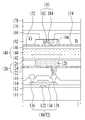
이러한 구동 박막트랜지스터(T2,130)는 도 3에 도시된 바와 같이 게이트 전극(132)과, 게이트 절연막(112)을 사이에 두고 게이트 전극(132)과 중첩되는 반도체층(134)과, 보호막(114) 상에 형성되어 반도체층(134)과 접촉하는 소스 및 드레인 전극(136,138)을 구비한다.3, the driving TFTs T2 and 130 include a
발광 소자(120)는 애노드 전극(122)과, 애노드 전극(122) 상에 형성되는 적어도 하나의 발광 스택(124)과, 발광 스택(124) 위에 형성된 캐소드 전극(126)을 구비한다.The
애노드 전극(122)은 평탄화막(116)을 관통하는 화소 컨택홀을 통해 노출된 구동 박막트랜지스터(130)의 드레인 전극(138)과 전기적으로 접속된다. 발광 스택(124)은 뱅크(128)에 의해 마련된 발광 영역의 애노드 전극(122) 상에 형성된다. 적어도 하나의 발광 스택(124) 각각은 정공 관련층, 유기 발광층, 전자 관련층 순으로 또는 역순으로 적층되어 형성되며, 컬러 필터(192)에 입사되는 백색광을 생성한다. 예를 들어, 발광 스택(124)은 전하 생성층을 사이에 두고 대향하는 제1 및 제2 발광 스택들을 구비한다. 이 경우, 제1 및 제2 발광 스택 중 어느 하나의 발광층은 청색광을 생성하고, 제1 및 제2 발광 스택 중 나머지 하나의 발광층은 노란색-녹색광을 생성함으로써 제1 및 제2 발광 스택을 통해 백색광이 생성된다. 캐소드 전극(126)은 발광 스택(124)을 사이에 두고 애노드 전극(122)과 대향하도록 형성된다.The
봉지부(140)는 외부의 수분이나 산소에 취약한 발광 소자(120)로 외부의 수분이나 산소가 침투되는 것을 차단한다. 이를 위해, 봉지부(140)는 다수의 무기 봉지층들(142,146)과, 다수의 무기 봉지층들(142,146) 사이에 배치되는 유기 봉지층(144)을 구비하며, 무기 봉지층(146)이 최상층에 배치되도록 한다. 이 때, 봉지부(140)는 적어도 2층의 무기 봉지층(142,146)과 적어도 1층의 유기 봉지층(144)을 구비한다. 본 발명에서는 제1 및 제2 무기 봉지층들(142,146) 사이에 유기 봉지층(144)이 배치되는 봉지부(140)의 구조를 예로 들어 설명하기로 한다.The sealing
제1 무기 봉지층(142)는 발광 소자(120)와 가장 인접하도록 캐소드 전극(126)이 형성된 기판(101) 상에 형성된다. 이러한 제1 무기 봉지층(142)은 질화실리콘(SiNx), 산화 실리콘(SiOx), 산화질화실리콘(SiON) 또는 산화 알루미늄(Al2O3)과 같은 저온 증착이 가능한 무기 절연 재질로 형성된다. 이에 따라, 제1 무기 봉지층(142)이 저온 분위기에서 증착되므로, 제1 무기 봉지층(142)의 증착 공정시 고온 분위기에 취약한 발광 스택(124)의 유기 발광층이 손상되는 것을 방지할 수 있다.The first
유기 봉지층(144)은 유기 발광 표시 장치의 휘어짐에 따른 각 층들 간의 응력을 완화시키는 완충역할을 하며, 평탄화 성능을 강화한다. 이 유기 봉지층(144)은 아크릴 수지, 에폭시 수지, 폴리이미드, 폴리에틸렌 또는 실리콘옥시카본(SiOC)과 같은 유기 절연 재질로 형성된다.The
제 2 무기 봉지층(146)는 유기 봉지층(144)이 형성된 기판(111) 상에 유기 봉지층(144) 및 제1 무기 봉지층(142) 각각의 상부면 및 측면을 덮도록 형성된다. 이에 따라, 제2 무기 봉지층(146)은 외부의 수분이나 산소가 제1 무기 봉지층(142) 및 유기 봉지층(144)으로 침투하는 것을 최소화하거나 차단한다. 이러한 제2 무기 봉지층(146)은 질화실리콘(SiNx), 산화 실리콘(SiOx), 산화질화실리콘(SiON) 또는 산화 알루미늄(Al2O3)과 같은 무기 절연 재질로 형성된다.The second
이러한 봉지부(140) 상에는 컬러 필터(192) 및 터치 센서(Cm)가 배치된다.On the sealing
컬러 필터(192)는 뱅크(128)에 의해 마련된 발광 영역과 중첩되도록 봉지부(140) 상에 직접 배치된다. 이에 따라, 발광 소자(120)에서 생성된 백색광이 컬러 필터(192)를 통해 출사됨으로써 컬러 영상을 구현할 수 있다. 한편, 컬러 필터(192)는 고온에 취약한 발광 스택(124)을 보호하기 위해 저온(약 100도이하)으로 제조될 수 있는 재질로 형성된다.The
이러한 컬러 필터(192)는 발광 소자(120)를 덮도록 형성된 봉지부(140) 상에 직접 배치된다. 이 경우, 컬러 필터(192) 및 발광 소자(120)가 동일 기판(111) 상에 배치되므로 본원 발명은 별도의 합착 공정이 불필요해져 공정이 단순화되며 비용을 저감할 수 있다. 반면에 종래 유기 발광 표시 장치는 컬러 필터(192) 및 발광 소자(120)가 서로 다른 기판 상에 배치되므로, 컬러 필터(192)가 형성된 기판과 발광 소자(120)가 형성된 기판을 합착하는 합착 공정이 필요해 공정이 복잡하고 비용이 상승하는 문제점이 있다.This
또한, 봉지부(140) 상에 컬러 필터(192)가 직접 배치된 본 발명에 따른 터치 센서를 가지는 유기 발광 표시 장치는 컬러 필터(192)가 형성된 별도의 기판 없이 발광 소자(120)가 형성된 기판만이 구비되므로 설계 자유도가 높아지고, 폴더블(Foldable)이 용이해진다. 뿐만 아니라, 본원 발명은 합착제가 불필요하므로 합착 얼라인 공차 및 합착제 두께만큼의 공간이 확보되어 해상도 및 개구율이 높아진다.The organic light emitting display device having the touch sensor according to the present invention in which the
이와 같이 본원 발명의 컬러 필터들(192) 사이에는 블랙매트릭스(194)가 배치되어 각 서브 화소 영역을 구분함과 아울러 인접한 서브 화소 영역 간의 광간섭 및 빛샘을 방지한다. 이 때, 블랙매트릭스(194)는 서브 화소 영역들 사이의 뱅크(128)와 중첩되도록 형성된다. 이러한 블랙매트릭스(194)는 고저항의 블랙 절연 재질로 형성되거나, 적색(R), 녹색(G) 및 청색(B) 컬러 필터(192) 중 적어도 2색의 컬러 필터가 적층되어 형성된다.In this way, a
컬러 필터들(192) 및 블랙매트릭스(194)가 형성된 기판(111) 상에 나란하게 형성된 터치 센싱 전극(152) 및 터치 구동 전극(154)을 포함하는 터치 센서(Cm)가 배치된다. 예를 들어, 터치 센싱 전극(152) 및 터치 구동 전극(154)은 동일 평면인 컬러 필터(192) 상에서 나란하게 배치된다.A touch sensor Cm including a
다수의 터치 센싱 전극(152)들은 컬러 필터(192) 및 블랙매트릭스(194) 상에서 또는 컬러 필터(192) 상에서 소정 방향을 따라 일정한 간격으로 이격된다.A plurality of
다수의 터치 구동 전극(154)들은 컬러 필터(192) 및 블랙매트릭스(194) 상에서 또는 컬러 필터(192) 상에서 터치 센싱 전극(152)과 나란한 방향을 따라 일정한 간격으로 이격된다. 이 때, 다수의 터치 구동 전극(154) 각각의 면적은 다수의 터치 센싱 전극(152) 각각의 면적보다 작게 형성된다. 이에 따라, 하나의 터치 센싱 전극(152)은 N(여기서, N은 1보다 큰 자연수) 개의 터치 구동 전극(154)과 대응된다.A plurality of
이러한 터치 센싱 전극(152)과 터치 구동 전극(154) 사이에는 상호 정전 용량(mutual capacitance)(Cm)이 형성된다. 이에 따라, 상호 정전 용량(Cm)은 터치 구동 전극(154)에 공급되는 터치 구동 펄스에 의해 전하를 충전하고, 충전된 전하를 터치 센싱 전극(152)으로 방전함으로써 터치 센서의 역할을 하게 된다.A mutual capacitance Cm is formed between the
한편, 본 발명의 터치 구동 전극(154) 및 터치 센싱 전극(152) 각각은 터치 구동 전극(154) 및 터치 센싱 전극(152) 사이에 배치되는 다수의 라우팅 라인(180)과 터치 패드(170)를 통해 터치 구동부(도시하지 않음)와 연결된다.Each of the
이에 따라, 라우팅 라인(180)은 터치 구동부에서 생성된 터치 구동 펄스를 터치 패드(170)를 통해 터치 구동 전극(154)에 전송하고, 터치 센싱 전극(152)으로부터의 터치 신호를 터치 패드(170)에 전송한다. 이를 위해, 라우팅 라인(180)은 터치 구동 전극(154) 및 터치 센싱 전극(152) 각각과 터치 패드(170) 사이를 연결하도록 배치되며, 별도의 컨택홀없이 터치 구동 전극(154) 및 터치 센싱 전극(152) 각각과 전기적으로 연결된다.The
라우팅 라인(180)은 Al, Ti, Cu, Mo와 같은 내식성 및 내산성이 강하고 전도성이 좋은 제1 도전층을 이용하여 단층 또는 다층 구조로 형성된다. 예를 들어, 라우팅 라인은 Ti/Al/Ti 또는 Mo/Al/Mo와 같이 적층된 3층 구조로 형성된다. 이외에도 라우팅 라인(180)은 도 3에 도시된 바와 같이 제1 및 제2 라우팅층(182,184)이 적층된 구조로 형성된다. 제1 라우팅층(182)은 Al, Ti, Cu, Mo와 같은 내식성 및 내산성이 강하고 전도성이 좋은 제1 도전층으로 형성되고, 제2 라우팅층(184)은 터치 구동 전극(154) 및 터치 센싱 전극(152)과 동일 재질인 내식성 및 내산성이 강한 ITO 또는 IZO와 같은 제2 도전층으로 형성된다.The
터치 패드(170)은 패드 전극(172)과, 그 패드 전극(172) 상에 패드 전극(172)을 덮도록 배치된 패드 커버 전극(174)으로 이루어진다.The
패드 전극(172)은 라우팅 라인(180)으로부터 신장되어 형성됨으로써 라우팅 라인(180)의 제1 라우팅층(182)과 동일 재질로 형성된다. 패드 커버 전극(174)은 터치 구동 전극(154) 및 터치 센싱 전극(152)과 동일 재질인 내식성 및 내산성이 강한 ITO 또는 IZO와 같은 제2 도전층으로 형성된다. 이러한 패드 커버 전극(174)은 터치 배리어 필름(176)에 의해 노출되도록 형성됨으로써 터치 구동부가 실장된 신호 전송 필름과 접속된다. 여기서, 터치 배리어 필름(176)은 터치 센싱 전극(152) 및 터치 구동 전극(154)과 컬러 필터(192)를 덮도록 형성되어 터치 센싱 전극(152) 및 터치 구동 전극(154)뿐만 아니라 발광 소자(120)가 외부의 수분 등에 의해 손상되는 것을 방지한다. 이러한 터치 배리어 필름(176)은 유기 절연 필름 상에 무기 절연막이 도포된 형태로 형성된다. 터치 배리어 필름(176) 상에는 원편광판 또는 휘도 향상 필름(OTF; Oled Transmittance Controllable Film)과 같은 광학 필름(178)이 배치될 수도 있다.The
이와 같이, 본 발명의 제1 실시 예에 따른 터치 센서를 가지는 유기 발광 표시 장치는 봉지부(140) 상에 터치 센싱 전극(152) 및 터치 구동 전극(154) 이 직접 배치된다. 이에 따라, 접착제를 통해 터치 스크린이 유기 발광 표시 장치에 접착되는 종래 유기 발광 표시 장치에 비해 본원 발명은 접착 공정이 불필요해져 공정이 단순화되며 비용을 저감할 수 있다. 또한, 본 발명에 따른 터치 센서를 가지는 유기 발광 표시 장치는 봉지부(140) 상에 컬러 필터(192)가 직접 배치된다. 이에 따라, 본원 발명은 합착 공정이 불필요해져 공정이 단순화되며 비용을 저감할 수 있으며, 폴더블(Foldable)이 용이해지며 고해상도 및 개구율이 높아진다.As described above, in the organic light emitting display device having the touch sensor according to the first embodiment of the present invention, the
도 4는 본 발명의 제2 실시 예에 따른 터치 센서를 가지는 유기 전계 발광 표시 장치를 나타내는 단면도이다.4 is a cross-sectional view illustrating an organic light emitting display device having a touch sensor according to a second embodiment of the present invention.
도 4에 도시된 터치 센서를 가지는 유기 발광 표시 장치는 도 3에 도시된 유기 발광 표시 장치와 대비하여 터치 구동 전극(154) 및 터치 센싱 전극(152)이 동일 평면인 터치 버퍼막(166) 상에 배치되는 것을 제외하고는 동일한 구성요소를 구비한다. 이에 따라, 동일한 구성요소에 대한 상세한 설명은 생략하기로 한다.The organic light emitting display having the touch sensor shown in FIG. 4 has a structure in which the
터치 버퍼막(166)은 컬러 필터(192) 및 블랙매트릭스(194)를 덮도록 이들 상에 형성되며, 터치 버퍼막(166) 상에 터치 구동 전극(154) 및 터치 센싱 전극(152)과 라우팅 라인(180)이 형성된다. 이 때, 터치 버퍼막(166)은 약 500Å~5㎛형성되어 터치 구동 전극(154) 및 터치 센싱 전극(152) 각각과, 캐소드 전극(126) 사이의 이격 거리가 최소 5㎛를 유지하도록 한다. 이에 따라, 터치 구동 전극(154) 및 터치 센싱 전극(152) 각각과, 캐소드 전극(126) 사이에 형성되는 기생커패시터의 용량값을 최소화할 수 있어 터치 구동 전극(154) 및 터치 센싱 전극(152) 각각과, 캐소드 전극(126) 간의 커플링(coupling)에 의한 상호 영향을 방지할 수 있다. 한편, 터치 구동 전극(154) 및 터치 센싱 전극(152) 각각과, 캐소드 전극(126) 사이의 이격 거리가 5㎛미만인 경우, 터치 구동 전극(154) 및 터치 센싱 전극(152) 각각과, 캐소드 전극(126) 간의 커플링(coupling)에 의한 상호 영향으로 터치 성능이 저하된다.The
또한, 터치 버퍼막(166)은 터치 구동 전극(154) 및 터치 센싱 전극(152)의 제조 공정시 이용되는 약액(현상액 또는 식각액 등등) 또는 외부로부터의 수분 등이 발광 스택(124)으로 침투되는 것을 차단할 수 있다. 이에 따라, 약액 또는 수분에 취약한 발광 스택(124)은 터치 버퍼막(166)에 의해 보호되므로 발광 스택(124)의 손상을 방지할 수 있다.In addition, the
이러한 터치 버퍼막(166)은 고온에 취약한 발광 스택(124)의 손상을 방지하기 위해 100도(℃) 이하의 저온에서 형성 가능하고 1~3의 저유전율을 가지는 유기 절연 재질로 형성된다. 예를 들어, 터치 버퍼막(166)은 아크릴 계열, 에폭시 계열 또는 실록산(Siloxan) 계열의 재질로 형성된다. 유기 절연 재질로 평탄화 성능을 가지는 터치 버퍼막(166)은 유기 발광 표시 장치의 휘어짐에 따른 봉지부(140) 내의 각 봉지층(142,144,146)의 손상 및 터치 버퍼막(166) 상에 형성되는 터치 센싱 전극(152) 및 터치 구동 전극(154)의 깨짐 현상을 방지할 수 있다.The
이와 같이, 본 발명의 제2 실시 예에 따른 터치 센서를 가지는 유기 발광 표시 장치는 봉지부(140) 상부에 터치 센싱 및 구동 전극들(152,154)이 직접 배치된다. 이에 따라, 접착제를 통해 터치 스크린이 유기 발광 표시 장치에 접착되는 종래 유기 발광 표시 장치에 비해 본원 발명은 접착 공정이 불필요해져 공정이 단순화되며 비용을 저감할 수 있다. 또한, 본 발명에 따른 터치 센서를 가지는 유기 발광 표시 장치는 봉지부(140) 상에 컬러 필터(192)가 직접 배치된다. 이에 따라, 본원 발명은 합착 공정이 불필요해져 공정이 단순화되며 비용을 저감할 수 있으며, 폴더블(Foldable)이 용이해지며 고해상도 및 개구율이 높아진다. 뿐만 아니라, 본 발명의 제2 실시 예에 따른 터치 센서를 가지는 유기 발광 표시 장치는 터치 구동 전극(154) 및 터치 센싱 전극(152)이 동일 평면인 터치 버퍼막(166) 상에 배치됨으로써 터치 버퍼막(166)을 통해 발광 스택(124)의 손상을 방지할 수 있음과 아울러 터치 구동 전극(154) 및 터치 센싱 전극(152)각각과 캐소드 전극(126) 사이에 형성되는 기생 커패시터의 용량값을 줄일 수 있다.As described above, in the organic light emitting diode display having the touch sensor according to the second embodiment of the present invention, the touch sensing and driving
도 5는 본 발명의 제3 실시 예에 따른 터치 센서를 가지는 유기 발광 표시 장치를 나타내는 단면도이다.5 is a cross-sectional view illustrating an organic light emitting display device having a touch sensor according to a third embodiment of the present invention.
도 5에 도시된 유기 발광 표시 장치는 도 4에 도시된 유기 발광 표시 장치와 대비하여 터치 구동 전극(154) 및 터치 센싱 전극(152)이 동일 평면인 봉지부(140)의 최상층인 제2 무기 봉지층(146) 상에서 나란하게 배치되고, 터치 구동 전극(154) 및 터치 센싱 전극(152) 상에 컬러 필터(192)가 배치되는 것을 제외하고는 동일한 구성요소를 구비한다. 이에 따라, 동일한 구성요소에 대한 상세한 설명은 생략하기로 한다.The organic light emitting display shown in FIG. 5 is different from the organic light emitting display shown in FIG. 4 in that the
도 5에 도시된 컬러 필터(192) 및 블랙매트릭스(194)는 터치 센서를 덮도록 배치된다. 즉, 터치 센서에 포함된 터치 구동 전극(154) 및 터치 센싱 전극(152)은 컬러 필터(192)와 봉지부(140) 사이에 배치된다. 이 때, 터치 센서(Cm)보다 상부에 위치하는 컬러 필터(192) 및 블랙매트릭스(194)는 유기 발광 표시 장치의 외부로부터 내부로 입사되는 외부광을 흡수한다. 즉, 터치 센서(Cm), 발광 소자(120) 및 박막트랜지스터(130) 각각에 포함된 반사율이 높은 금속으로 형성된 도전층(예를 들어, 브릿지(152b,154b), 애노드 전극(122), 게이트 전극(132), 소스 및 드레인 전극(136,138))에 의해 외부광이 반사되는 것을 방지할 수 있어 외부광에 의해 시인성이 저하되는 것을 방지한다. 이에 따라, 도 5에 도시된 유기 발광 표시 장치는 별도의 원편광판 없이도 외부광에 의해 시인성이 저하되는 것을 방지할 수 있으므로, 원편광판의 제거로 비용을 절감할 수 있다.The
또한, 컬러 필터(192) 및 블랙매트릭스(194)가 형성된 기판(111) 상에 터치 버퍼막(166)이 형성된다. 터치 버퍼막(166)은 아크릴 수지, 에폭시 수지, 폴리이미드, 폴리에틸렌 또는 실리콘옥시카본(SiOC)과 같은 유기 절연 재질로 형성된다. 이러한 유기 절연 재질로 형성된 터치 버퍼막(166)에 의해 컬러 필터(192) 및 블랙매트릭스(194)가 형성된 기판(111)이 평탄화되므로, 터치 버퍼막(166) 상에 부착되는 배리어 필름(176) 및 광학 필름(178)의 접착력이 향상된다.A
이와 같이, 본 발명의 제3 실시 예에 따른 터치 센서를 가지는 유기 발광 표시 장치는 봉지부(140) 상에 터치 구동 전극(154) 및 터치 센싱 전극(152)이 직접 배치된다. 이에 따라, 접착제를 통해 터치 스크린이 유기 발광 표시 장치에 접착되는 종래 유기 발광 표시 장치에 비해 본원 발명은 접착 공정이 불필요해져 공정이 단순화되며 비용을 저감할 수 있다. 또한, 본 발명에 따른 터치 센서를 가지는 유기 발광 표시 장치는 봉지부(140) 상에 컬러 필터(192)가 직접 배치된다. 이에 따라, 본원 발명은 합착 공정이 불필요해져 공정이 단순화되며 비용을 저감할 수 있으며, 폴더블(Foldable)이 용이해지며 고해상도 및 개구율이 높아진다. 뿐만 아니라, 본 발명에 따른 터치 센서를 가지는 유기 발광 표시 장치는 발광 소자(120) 및 터치 센서(Cm)를 덮도록 배치되는 컬러 필터(192) 및 블랙매트릭스(194)를 통해 외부광을 흡수하므로, 외부광에 의해 시인성이 저하되는 것을 방지할 수 있다.As described above, in the OLED display device having the touch sensor according to the third embodiment of the present invention, the
도 6은 본 발명의 제4 실시 예에 따른 터치 센서를 가지는 유기 발광 표시 장치를 나타내는 단면도이다.6 is a cross-sectional view illustrating an OLED display device having a touch sensor according to a fourth embodiment of the present invention.
도 6에 도시된 유기 발광 표시 장치는 도 5에 도시된 유기 발광 표시 장치와 대비하여 터치 배리어 필름(176)을 생략하고 배리어 박막층(160)을 구비하는 것을 제외하고는 동일한 구성요소를 구비한다. 이에 따라, 동일한 구성요소에 대한 상세한 설명은 생략하기로 한다.The organic light emitting display shown in FIG. 6 has the same components as the organic light emitting display shown in FIG. 5 except that the touching
배리어 박막층(160)은 봉지부(140)의 최상층과, 터치 구동 전극(154) 및 터치 센싱 전극(152) 사이에 형성되거나, 발광 소자(120) 및 봉지부(140)의 최하층 사이에 형성된다. 예를 들어, 배리어 박막층(160)은 캐소드 전극(126)과 봉지부(140)의 최하층에 위치하는 제1 무기 봉지층(142) 사이에 형성된다. 이 배리어 박막층(160)은 원자층 증착 (Atomic Layer Deposition; ALD) 방식으로 형성되는 무기물층, 질화실리콘(SiNx), 산화 실리콘(SiOx), 산화질화실리콘(SiON) 또는 산화 알루미늄(Al2O3)과 같은 저온 증착이 가능한 무기 절연 재질로 형성된다. 이에 따라, 배리어 박막층(160)은 외부의 수분이나 산소에 취약한 발광 소자(120)로 외부의 수분이나 산소가 침투되는 것을 차단함으로써 별도의 터치 배리어 필름을 생략할 수 있다. 또한, 배리어 박막층(160)이 저온 증착 공정을 통해 형성되므로, 고온 분위기에 취약한 발광 스택(124)이 손상되는 것을 방지할 수 있다.The barrier
도 7a 내지 도 7b는 본 발명의 제1 내지 제4 실시 예에 따른 유기 발광 표시 장치의 터치 센서의 제조 방법을 설명하기 위한 단면도들이다. 여기서, 도 4에 도시된 본 발명의 제2 실시 예의 구조를 예로 들어 설명하기로 한다.FIGS. 7A and 7B are cross-sectional views illustrating a method of manufacturing a touch sensor of an OLED display according to the first through fourth embodiments of the present invention. Here, the structure of the second embodiment of the present invention shown in Fig. 4 will be described as an example.
도 7a를 참조하면, 스위칭 트랜지스터, 구동 트랜지스터(130), 발광 소자(120), 봉지부(140), 블랙매트릭스(194), 컬러 필터(192) 및 터치 버퍼막(166)이 형성된 기판(111) 상에 라우팅 라인의 제1 라우팅층(182) 및 패드 전극(172)이 형성된다.7A, a
구체적으로, 스위칭 트랜지스터, 구동 트랜지스터, 발광 소자(120), 봉지부(140), 블랙매트릭스(194), 컬러 필터(192) 및 터치 버퍼막(166)이 형성된 기판(111) 상에 제1 도전층이 스퍼터링을 이용한 증착 공정을 통해 상온에서 전면 증착된 후, 제1 마스크를 이용한 포토리소그래피 공정과 식각 공정으로 제1 도전층이 패터닝됨으로써 라우팅 라인의 제1 라우팅층(182)과 패드 전극(172)이 형성된다. 여기서, 제1 도전층은 Al, Ti, Cu, Mo와 같은 내식성 및 내산성이 강한 금속을 이용하여 단층 또는 다층 구조로 형성된다. 예를 들어, 제1 도전층은 Ti/Al/Ti 또는 Mo/Al/Mo와 같이 적층된 3층 구조로 형성된다.Specifically, on the
도 7b를 참조하면, 라우팅 라인의 제1 라우팅층(182) 및 패드 전극(172)이 형성된 기판(111) 상에 터치 구동 전극(154), 터치 센싱 전극(152), 라우팅 라인의 제2 라우팅층(184) 및 패드 커버 전극(174)이 형성된다.Referring to FIG. 7B, on the
구체적으로, 라우팅 라인의 제1 라우팅층(182) 및 패드 전극(172)이 형성된 기판(111) 상에 제2 도전층이 전면 증착된다. 여기서, 제2 도전층으로 ITO 또는 IZO와 같은 투명 도전층이 이용되는 경우, 투명 도전층은 상온에서 스퍼터링 등과 같은 증착 방법으로 상온으로 형성된다. 그런 다음, 제2 도전층이 제2 마스크를 이용한 포토리소그래피 공정과 식각 공정으로 패터닝됨으로써 터치 구동 전극(154), 터치 센싱 전극(152), 라우팅 라인의 제2 라우팅층(184) 및 패드 커버 전극(174)이 형성된다. 그런 다음, 터치 구동 전극(154), 터치 센싱 전극(152), 라우팅 라인의 제2 라우팅층(184) 및 패드 커버 전극(174)이 형성된 기판(111) 상에 터치 배리어 필름(176) 및 광학 필름(178)이 부착된다.Specifically, the second conductive layer is entirely deposited on the
도 8은 본 발명의 제5 실시 예에 따른 터치 센서를 가지는 유기 발광 표시 장치를 나타내는 평면도 및 단면도이다.8 is a plan view and a cross-sectional view illustrating an organic light emitting display device having a touch sensor according to a fifth embodiment of the present invention.
도 8에 도시된 유기 발광 표시 장치는 도 3 내지 도 6에 도시된 유기 발광 표시 장치와 대비하여 터치 구동 전극(154) 및 터치 센싱 전극(152)의 구성이 달라지는 것을 제외하고는 동일한 구성요소를 구비한다. 이에 따라, 동일한 구성요소에 대한 상세한 설명은 설명하기로 한다.The organic light emitting display shown in FIG. 8 has the same components as those of the organic light emitting display shown in FIGS. 3 to 6 except that the configurations of the
도 8에 도시된 바와 같이, 터치 구동 전극(154) 및 터치 센싱 전극(152)은 메쉬 형태로 형성될 수도 있다. 즉, 터치 구동 전극(154) 및 터치 센싱 전극(152)은 도 9a 및 도 9b에 도시된 바와 같이 투명 도전막(153)과, 그 투명 도전막(153)의 상부 또는 하부에 메쉬 형태로 형성된 메쉬 금속막(151)으로 이루어진다. 메쉬 금속막(151)은 라우팅 라인(180)의 제1 라우팅층(182)과 동일 재질로 제1 라우팅층(182)과 동일 마스크 공정으로 형성된다. 이에 따라, 메쉬 금속막(151)으로 인해 제조 공정이 복잡해지고 비용이 상승하는 것을 방지할 수 있다.As shown in FIG. 8, the
이외에도 터치 구동 전극(154) 및 터치 센싱 전극(152)은 투명 도전막(153)없이 메쉬 금속막(151)으로만 이루어지거나, 메쉬 금속막(151) 없이 투명 도전막(153)이 메쉬 형태로 형성될 수도 있다. 여기서, 메쉬 금속막(151)은 투명 도전막(153)보다 전도성이 좋아 터치 구동 전극(154) 및 터치 센싱 전극(152) 각각을 저저항 전극으로 형성할 수 있다. 특히, 고온에 취약한 발광 스택(124)을 보호하기 위해 투명 도전막(153)을 저온(약 100도이하)에서 형성하는 경우, 투명 도전막(153)이 고투명 및 저저항 특성을 얻기 어렵다. 이 경우, 전도성이 좋은 메쉬 금속막(151)을 통해 터치 구동 전극(154) 및 터치 센싱 전극(152) 각각의 저항 특성을 낮추면서 투명 도전막(153)의 두께를 얇게 형성하여 투과율을 증가시킬 수 있다.The
이에 따라, 터치 구동 전극(154) 및 터치 센싱 전극(152) 자체의 저항과 커패시턴스 감소되어 RC 시정수가 감소되어 터치 감도를 향상시킬 수 있다. 또한, 메쉬 금속막(151)의 선폭이 매우 얇아 메쉬 금속막(151)으로 인해 개구율 및 투과율이 저하되는 것을 방지할 수 있다.Accordingly, the resistance and capacitance of the
이상의 설명은 본 발명을 예시적으로 설명한 것에 불과하며, 본 발명이 속하는 기술 분야에서 통상의 지식을 가진 자에 의해 본 발명의 기술적 사상에서 벗어나지 않는 범위에서 다양한 변형이 가능할 것이다. 따라서 본 발명의 명세서에 개시된 실시 예들은 본 발명을 한정하는 것이 아니다. 본 발명의 범위는 아래의 특허청구범위에 의해 해석되어야 하며, 그와 균등한 범위 내에 있는 모든 기술도 본 발명의 범위에 포함되는 것으로 해석해야 할 것이다.The foregoing description is merely illustrative of the present invention, and various modifications may be made by those skilled in the art without departing from the spirit of the present invention. Accordingly, the embodiments disclosed in the specification of the present invention are not intended to limit the present invention. The scope of the present invention should be construed according to the following claims, and all the techniques within the scope of equivalents should be construed as being included in the scope of the present invention.
142,144 : 무기 봉지층 146 : 유기 봉지층
152 : 터치 센싱 전극 154 : 터치 구동 전극
192 : 컬러 필터 194 : 블랙매트릭스142, 144: inorganic encapsulating layer 146: organic encapsulating layer
152: touch sensing electrode 154: touch driving electrode
192: Color filter 194: Black matrix
Claims (16)
Translated fromKorean상기 발광 소자 상에 배치되는 봉지부와;
상기 봉지부 상부에 배치되는 컬러 필터와;
상기 봉지부 상부의 동일 평면 상에서 나란하게 배치되는 터치 센싱 전극 및 터치 구동 전극과;
상기 발광 소자 및 상기 봉지부가 배치된 상기 기판 상에서 상기 터치 센싱 전극 및 상기 터치 구동 전극 각각과 접속되며 상기 봉지부의 측면을 따라서 형성되는 라우팅 라인을 구비하는 유기 발광 표시 장치.A light emitting element disposed on the substrate;
An encapsulant disposed on the light emitting device;
A color filter disposed above the sealing portion;
A touch sensing electrode and a touch driving electrode arranged on the same plane on the upper portion of the sealing portion;
And a routing line connected to each of the touch sensing electrode and the touch driving electrode on the substrate on which the light emitting device and the sealing portion are disposed, the routing line being formed along the side surface of the sealing portion.
상기 터치 센싱 전극 및 터치 구동 전극은 상기 컬러 필터 상에서 나란하게 배치되는 유기 발광 표시 장치.The method according to claim 1,
Wherein the touch sensing electrode and the touch driving electrode are arranged side by side on the color filter.
상기 컬러 필터 상에 배치되는 터치 버퍼막을 추가로 구비하며,
상기 터치 센싱 전극 및 터치 구동 전극은 상기 터치 버퍼막 상에서 나란하게 배치되는 유기 발광 표시 장치.The method according to claim 1,
Further comprising a touch buffer film disposed on the color filter,
Wherein the touch sensing electrode and the touch driving electrode are arranged in parallel on the touch buffer film.
상기 터치 센싱 전극 및 터치 구동 전극은 상기 컬러 필터와 상기 봉지부 사이에 배치되는 유기 발광 표시 장치.The method according to claim 1,
Wherein the touch sensing electrode and the touch driving electrode are disposed between the color filter and the sealing portion.
상기 터치 센싱 전극 및 터치 구동 전극은 상기 봉지부의 최상층 상에서 나란하게 배치되는 유기 발광 표시 장치.5. The method of claim 4,
Wherein the touch sensing electrode and the touch driving electrode are arranged in parallel on the uppermost layer of the sealing portion.
상기 터치 센싱 전극, 터치 구동 전극 및 상기 컬러 필터를 덮도록 배치되는 배리어 필름을 추가로 구비하는 유기 발광 표시 장치.6. The method according to any one of claims 1 to 5,
And a barrier film disposed to cover the touch sensing electrode, the touch driving electrode, and the color filter.
상기 봉지부 및 상기 발광 소자 사이에 배치되거나, 상기 봉지부 상에 배치되는 배리어 박막층을 추가로 구비하는 유기 발광 표시 장치.6. The method according to any one of claims 1 to 5,
And a barrier thin film layer disposed between the encapsulation part and the light emitting element or disposed on the encapsulation part.
상기 터치 센싱 전극 및 터치 구동 전극은 메쉬 형태의 금속막과, 상기 금속막의 상부 및 하부에 상기 금속막보다 넓은 선폭으로 배치되는 투명 도전막을 구비하는 유기 발광 표시 장치.6. The method according to any one of claims 1 to 5,
Wherein the touch sensing electrode and the touch driving electrode comprise a metal film in a mesh form and a transparent conductive film disposed on upper and lower portions of the metal film in a line width wider than the metal film.
상기 발광 소자는
상기 기판 상에 배치되는 애노드 전극과;
상기 애노드 전극과 대향하는 캐소드 전극과;
상기 애노드 전극 및 캐소드 전극 사이에 배치되며 상기 컬러 필터에 입사되는 백색광을 생성하는 적어도 하나의 발광 스택을 구비하는 유기 발광 표시 장치.The method according to claim 1,
The light-
An anode electrode disposed on the substrate;
A cathode electrode facing the anode electrode;
And at least one light emitting stack disposed between the anode electrode and the cathode electrode and generating white light incident on the color filter.
상기 발광 소자 상에 배치되는 봉지부를 형성하는 단계와;
상기 봉지부 상부에 배치되는 컬러 필터를 형성하는 단계와;
상기 봉지부 상부의 동일 평면 상에서 나란하게 배치되는 터치 센싱 전극 및 터치 구동 전극을 형성하고, 상기 발광 소자 및 상기 봉지부가 배치된 상기 기판 상에서 상기 터치 센싱 전극 및 상기 터치 구동 전극 각각과 접속되는 라우팅 라인을 형성하는 단계를 포함하며,
상기 라우팅 라인은 상기 봉지부의 측면을 따라서 형성되는 유기 발광 표시 장치의 제조 방법.Forming a light emitting element disposed on a substrate;
Forming an encapsulant disposed on the light emitting element;
Forming a color filter disposed above the sealing portion;
A touch sensing electrode and a touch driving electrode arranged in parallel on the same plane of the encapsulation unit and electrically connected to the touch sensing electrode and the touch driving electrode on the substrate on which the light emitting device and the encapsulation unit are disposed, , ≪ / RTI >
Wherein the routing line is formed along a side surface of the sealing portion.
상기 터치 센싱 전극 및 터치 구동 전극을 형성하는 단계는 상기 컬러 필터 상에서 나란하게 배치되는 상기 터치 센싱 전극 및 터치 구동 전극을 형성하는 단계인 유기 발광 표시 장치의 제조 방법.11. The method of claim 10,
Wherein the forming of the touch sensing electrode and the touch driving electrode comprises forming the touch sensing electrode and the touch driving electrode arranged in parallel on the color filter.
상기 컬러 필터 상에 배치되는 터치 버퍼막을 형성하는 단계를 추가로 포함하며,
상기 터치 센싱 전극 및 터치 구동 전극을 형성하는 단계는 상기 터치 버퍼막 상에서 나란하게 배치되는 상기 터치 센싱 전극 및 터치 구동 전극을 형성하는 단계인 유기 발광 표시 장치의 제조 방법.11. The method of claim 10,
Further comprising forming a touch buffer film disposed on the color filter,
Wherein the forming of the touch sensing electrode and the touch driving electrode comprises forming the touch sensing electrode and the touch driving electrode arranged side by side on the touch buffer film.
상기 터치 센싱 전극 및 터치 구동 전극을 형성하는 단계는 상기 컬러 필터와 상기 봉지부 사이에 배치되도록 상기 터치 센싱 전극 및 터치 구동 전극을 형성하는 단계인 유기 발광 표시 장치의 제조 방법.11. The method of claim 10,
Wherein the forming of the touch sensing electrode and the touch driving electrode comprises forming the touch sensing electrode and the touch driving electrode so as to be disposed between the color filter and the sealing portion.
상기 터치 센싱 전극 및 터치 구동 전극을 형성하는 단계는 상기 봉지부의 최상층 상에서 나란하게 배치되는 상기 터치 센싱 전극 및 터치 구동 전극을 형성하는 단계인 유기 발광 표시 장치의 제조 방법.14. The method of claim 13,
Wherein the step of forming the touch sensing electrode and the touch driving electrode is a step of forming the touch sensing electrode and the touch driving electrode arranged side by side on the uppermost layer of the sealing portion.
상기 터치 센싱 전극, 터치 구동 전극 및 상기 컬러 필터를 덮도록 배치되는 배리어 필름을 형성하는 단계를 추가로 포함하는 유기 발광 표시 장치의 제조 방법.15. The method according to any one of claims 10 to 14,
And forming a barrier film covering the touch sensing electrode, the touch driving electrode, and the color filter.
상기 봉지부 및 상기 발광 소자 사이에 배치되거나, 상기 봉지부 상에 배치되는 배리어 박막층을 형성하는 단계를 추가로 포함하는 유기 발광 표시 장치의 제조 방법.15. The method according to any one of claims 10 to 14,
And forming a barrier thin film layer disposed between the encapsulation part and the light emitting element or disposed on the encapsulation part.
Priority Applications (6)
| Application Number | Priority Date | Filing Date | Title |
|---|---|---|---|
| KR1020160126760AKR101992915B1 (en) | 2016-09-30 | 2016-09-30 | Organic light emitting display with touch sensor and fabricating method thereof |
| CN201710072738.2ACN107885379B (en) | 2016-09-30 | 2017-02-10 | Display device with touch sensor |
| EP17156042.8AEP3301548B1 (en) | 2016-09-30 | 2017-02-14 | Display device with touch sensor |
| TW108118778ATWI733121B (en) | 2016-09-30 | 2017-02-17 | Light emitting display device with touch sensor |
| TW106105297ATWI712195B (en) | 2016-09-30 | 2017-02-17 | Light emitting display device with touch sensor |
| US15/438,302US10809829B2 (en) | 2016-09-30 | 2017-02-21 | Display device with touch sensor |
Applications Claiming Priority (1)
| Application Number | Priority Date | Filing Date | Title |
|---|---|---|---|
| KR1020160126760AKR101992915B1 (en) | 2016-09-30 | 2016-09-30 | Organic light emitting display with touch sensor and fabricating method thereof |
Related Child Applications (1)
| Application Number | Title | Priority Date | Filing Date |
|---|---|---|---|
| KR1020190068531ADivisionKR102037851B1 (en) | 2019-06-11 | 2019-06-11 | Display device and fabricating method thereof |
Publications (2)
| Publication Number | Publication Date |
|---|---|
| KR20180036324A KR20180036324A (en) | 2018-04-09 |
| KR101992915B1true KR101992915B1 (en) | 2019-06-25 |
Family
ID=58043963
Family Applications (1)
| Application Number | Title | Priority Date | Filing Date |
|---|---|---|---|
| KR1020160126760AActiveKR101992915B1 (en) | 2016-09-30 | 2016-09-30 | Organic light emitting display with touch sensor and fabricating method thereof |
Country Status (5)
| Country | Link |
|---|---|
| US (1) | US10809829B2 (en) |
| EP (1) | EP3301548B1 (en) |
| KR (1) | KR101992915B1 (en) |
| CN (1) | CN107885379B (en) |
| TW (2) | TWI712195B (en) |
Cited By (1)
| Publication number | Priority date | Publication date | Assignee | Title |
|---|---|---|---|---|
| US11650681B2 (en) | 2020-02-20 | 2023-05-16 | Samsung Display Co., Ltd. | Display device |
Families Citing this family (28)
| Publication number | Priority date | Publication date | Assignee | Title |
|---|---|---|---|---|
| KR101974086B1 (en)* | 2016-09-30 | 2019-05-02 | 삼성디스플레이 주식회사 | Display module |
| CN206685388U (en)* | 2017-03-14 | 2017-11-28 | 京东方科技集团股份有限公司 | A kind of encapsulating structure, display panel and display device |
| KR102330862B1 (en)* | 2017-04-27 | 2021-11-24 | 엘지디스플레이 주식회사 | Display device and method of fabricating the same |
| CN107180852B (en)* | 2017-05-18 | 2019-11-15 | 上海天马有机发光显示技术有限公司 | A kind of touch display panel and display device |
| JP6942602B2 (en)* | 2017-10-19 | 2021-09-29 | 株式会社ジャパンディスプレイ | Display device manufacturing method |
| CN107946346A (en)* | 2017-11-24 | 2018-04-20 | 武汉华星光电半导体显示技术有限公司 | A kind of full frame fingerprint recognition touching display screen |
| FR3079909B1 (en)* | 2018-04-05 | 2022-10-14 | Microoled | ELECTROLUMINESCENT DEVICE WITH IMPROVED RESOLUTION AND RELIABILITY |
| CN108761995A (en)* | 2018-06-21 | 2018-11-06 | 京东方科技集团股份有限公司 | Mask plate, exposure method and touch panel |
| KR102262165B1 (en) | 2018-08-08 | 2021-06-09 | 삼성전자주식회사 | Electronic device for controlling communication connection with input device and method for controlling thereof |
| CN109192762B (en)* | 2018-09-06 | 2021-01-15 | 京东方科技集团股份有限公司 | Display substrate, method for manufacturing the same, and display device |
| TWI683248B (en)* | 2018-11-12 | 2020-01-21 | 友達光電股份有限公司 | Touch panel and manufacturing method thereof |
| KR102717697B1 (en)* | 2019-01-25 | 2024-10-17 | 삼성디스플레이 주식회사 | Display device having touch sensor |
| KR20200097374A (en)* | 2019-02-07 | 2020-08-19 | 삼성디스플레이 주식회사 | Electronic panel and electronic apparatus including the same |
| KR102856743B1 (en)* | 2019-07-17 | 2025-09-08 | 삼성디스플레이 주식회사 | Display device |
| CN110379939B (en)* | 2019-07-26 | 2022-04-26 | 京东方科技集团股份有限公司 | Display panel, manufacturing method thereof and display device |
| KR102800614B1 (en)* | 2019-08-26 | 2025-04-25 | 삼성디스플레이 주식회사 | Display device and method for manufacturing the same |
| KR20210086245A (en) | 2019-12-31 | 2021-07-08 | 엘지디스플레이 주식회사 | Organic light emitting diode display device including touch sensor and manufacturing method thereof |
| KR20210151300A (en) | 2020-06-04 | 2021-12-14 | 삼성디스플레이 주식회사 | Display apparatus |
| KR102839630B1 (en)* | 2020-12-30 | 2025-07-28 | 엘지디스플레이 주식회사 | Display device |
| KR20220096896A (en) | 2020-12-31 | 2022-07-07 | 엘지디스플레이 주식회사 | Transparent Touch Display apparatus |
| CN215578574U (en)* | 2021-01-26 | 2022-01-18 | 京东方科技集团股份有限公司 | Display substrate and display device |
| KR102397356B1 (en)* | 2021-03-10 | 2022-05-12 | 이성호 | Detectors consisting of multiple different areas and object detection devices using them |
| EP4206882A4 (en) | 2021-05-19 | 2024-01-03 | BOE Technology Group Co., Ltd. | Touch structure and display panel |
| KR20220158909A (en)* | 2021-05-24 | 2022-12-02 | 삼성디스플레이 주식회사 | Electronic device |
| JP2023037375A (en)* | 2021-09-03 | 2023-03-15 | 株式会社ジャパンディスプレイ | Sensor module and display device including sensor module |
| CN114267807B (en)* | 2021-12-15 | 2023-08-22 | 武汉华星光电半导体显示技术有限公司 | Display panel |
| CN116414259A (en)* | 2022-01-04 | 2023-07-11 | 京东方科技集团股份有限公司 | Touch display panel and display device |
| US12416991B2 (en) | 2023-10-13 | 2025-09-16 | Sung Ho Lee | Object sensing device and sensing method composed of different CDA areas |
Family Cites Families (71)
| Publication number | Priority date | Publication date | Assignee | Title |
|---|---|---|---|---|
| US20060231848A1 (en) | 2005-04-14 | 2006-10-19 | Chien-Kun Fu | Light emitting diode package for enhancing light extraction |
| KR100873080B1 (en)* | 2007-05-10 | 2008-12-09 | 삼성모바일디스플레이주식회사 | Organic electroluminescent display |
| TWI413249B (en)* | 2008-10-22 | 2013-10-21 | Wintek Corp | Organic light emitting diode display device and method of manufacturing same |
| TWI380089B (en)* | 2008-12-03 | 2012-12-21 | Au Optronics Corp | Method of forming a color filter touch sensing substrate |
| CN101887904B (en)* | 2009-05-15 | 2013-02-06 | 上海天马微电子有限公司 | Organic light emitting diode display integrated with touch screen |
| KR20110037337A (en)* | 2009-10-06 | 2011-04-13 | 엘지디스플레이 주식회사 | Organic light emitting display device and manufacturing method thereof |
| KR101073147B1 (en)* | 2010-04-05 | 2011-10-12 | 삼성모바일디스플레이주식회사 | Touch screen panel integrated flat panel display and manufacturing method |
| JP5443251B2 (en)* | 2010-04-21 | 2014-03-19 | 株式会社ジャパンディスプレイ | Touch panel and display device |
| KR101886801B1 (en) | 2010-09-14 | 2018-08-10 | 삼성디스플레이 주식회사 | flat panel display integrated touch screen panel |
| KR101692896B1 (en)* | 2010-10-25 | 2017-01-05 | 엘지디스플레이 주식회사 | Organic electro luminescent device having touch sensing function |
| KR101178914B1 (en)* | 2010-10-29 | 2012-09-03 | 삼성디스플레이 주식회사 | flat panel display integrated touch screen panel |
| EP2538313B1 (en)* | 2011-06-20 | 2015-05-20 | Melfas, Inc. | Touch sensor panel |
| US9292143B2 (en)* | 2011-07-29 | 2016-03-22 | Sharp Kabushiki Kaisha | Touch panel substrate and electro-optical device |
| US9285842B2 (en)* | 2011-07-29 | 2016-03-15 | Sharp Kabushiki Kaisha | Touch panel substrate and electro-optic device |
| US20130081869A1 (en)* | 2011-09-30 | 2013-04-04 | Jae Hong Kim | Touch sensing apparatus and method of manufacturing the same |
| KR101380479B1 (en)* | 2012-03-30 | 2014-04-01 | 엘지디스플레이 주식회사 | Touch screen integrated display device and method of fabricating the same |
| KR101469485B1 (en) | 2012-08-13 | 2014-12-05 | 엘지디스플레이 주식회사 | Organic Emitting Display Device and Method for Manufacturing the Same |
| CN103293735B (en)* | 2012-08-27 | 2015-11-25 | 上海天马微电子有限公司 | Touch control type liquid crystal display device |
| US20140062916A1 (en)* | 2012-08-28 | 2014-03-06 | Lg Display Co., Ltd. | Touch panel and method of manufacturing the same and display device using the same |
| KR101975535B1 (en)* | 2012-09-11 | 2019-05-08 | 삼성디스플레이 주식회사 | flexible touch screen panel |
| CN103163676B (en)* | 2012-09-26 | 2016-03-09 | 敦泰电子有限公司 | The liquid crystal display touch screen of integrated single-layer capacitance sensor and application apparatus thereof |
| KR101930383B1 (en)* | 2012-10-31 | 2019-03-11 | 엘지디스플레이 주식회사 | Organic Light Emitting Device and Method of manufacturing the same |
| KR101615791B1 (en)* | 2012-11-14 | 2016-04-26 | 엘지디스플레이 주식회사 | None-Bezel Display Panel Having Edge Bending Structure |
| KR102043847B1 (en)* | 2012-11-16 | 2019-11-13 | 엘지디스플레이 주식회사 | Electrostatic capacitive type touch screen panel |
| US9853092B2 (en)* | 2012-11-30 | 2017-12-26 | Lg Display Co., Ltd. | OLED display device having touch sensor and method of manufacturing the same |
| KR101980756B1 (en)* | 2012-12-07 | 2019-05-21 | 엘지디스플레이 주식회사 | Organic light emitting diode display device including touch panel |
| KR101318448B1 (en)* | 2012-12-11 | 2013-10-16 | 엘지디스플레이 주식회사 | Touch sensor integrated type display device and method of fabricating the same |
| KR101980766B1 (en)* | 2012-12-27 | 2019-05-21 | 엘지디스플레이 주식회사 | Organic light emitting diode display device including touch panel |
| KR102245511B1 (en)* | 2012-12-27 | 2021-04-28 | 엘지디스플레이 주식회사 | Flexible organic light emitting display device and method for manufacturing the same |
| US9740035B2 (en)* | 2013-02-15 | 2017-08-22 | Lg Display Co., Ltd. | Flexible organic light emitting display device and method for manufacturing the same |
| JP6139196B2 (en)* | 2013-03-15 | 2017-05-31 | 株式会社ジャパンディスプレイ | ORGANIC ELECTROLUMINESCENT DISPLAY DEVICE AND METHOD FOR PRODUCING ORGANIC ELECTROLUMINESCENT DISPLAY DEVICE |
| KR101625176B1 (en)* | 2013-04-22 | 2016-05-27 | 엘지디스플레이 주식회사 | Color Filter Substrate for Display Device with Integrated Touch Screen and Method for Fabricating The Same |
| KR102046296B1 (en)* | 2013-04-26 | 2019-11-19 | 엘지디스플레이 주식회사 | Touch-Type Organic Light-Emitting Diode Display Device |
| KR101588499B1 (en)* | 2013-07-24 | 2016-01-25 | 주식회사 엘지화학 | Structure of flexible printed circuit board |
| KR20150024572A (en)* | 2013-08-27 | 2015-03-09 | 엘지이노텍 주식회사 | Touch window and display with the same |
| KR101641690B1 (en)* | 2013-09-25 | 2016-07-21 | 엘지디스플레이 주식회사 | Display device with integrated touch screen |
| KR101692351B1 (en)* | 2013-11-27 | 2017-01-03 | 엘지디스플레이 주식회사 | Organic Light Emitting Display Apparatus and Method for Manufacturing The Same |
| KR102162912B1 (en)* | 2013-12-06 | 2020-10-07 | 엘지디스플레이 주식회사 | Organic electroluminescent device having touch panel and method for fabricating the same |
| KR20150072467A (en)* | 2013-12-19 | 2015-06-30 | 주성엔지니어링(주) | Apparatus, system and method of manufacturing a touch panel |
| KR102124906B1 (en)* | 2013-12-26 | 2020-07-07 | 엘지디스플레이 주식회사 | Organic electro luminescent device having touch screen and method of fabricationg the same |
| KR102174679B1 (en)* | 2013-12-31 | 2020-11-06 | 엘지디스플레이 주식회사 | Touch panel |
| KR102168132B1 (en)* | 2013-12-31 | 2020-10-21 | 삼성디스플레이 주식회사 | Organic light emitting device |
| KR102191575B1 (en)* | 2014-01-13 | 2020-12-15 | 엘지이노텍 주식회사 | Touch window and display with the same |
| KR102187680B1 (en)* | 2014-02-13 | 2020-12-07 | 엘지이노텍 주식회사 | Touch window |
| KR102245943B1 (en)* | 2014-06-23 | 2021-04-29 | 엘지디스플레이 주식회사 | Touch panel and apparatus for driving thereof |
| CN104252276B (en)* | 2014-06-30 | 2018-04-27 | 上海天马有机发光显示技术有限公司 | A kind of touch control display apparatus and its manufacture method |
| US10775913B2 (en)* | 2014-06-30 | 2020-09-15 | Lg Display Co., Ltd. | Touch sensor integrated display device and method of manufacturing the same |
| KR102215750B1 (en)* | 2014-07-15 | 2021-02-17 | 삼성디스플레이 주식회사 | Laser anneal apparatus and laser anneal method using the same |
| KR102417018B1 (en)* | 2014-08-26 | 2022-07-05 | 엘지디스플레이 주식회사 | Apparatus for driving of touch panel |
| KR102295614B1 (en)* | 2014-09-29 | 2021-08-27 | 엘지디스플레이 주식회사 | Organic light emitting display device |
| KR102240937B1 (en)* | 2014-10-10 | 2021-04-15 | 삼성디스플레이 주식회사 | Display device |
| US9958973B2 (en)* | 2014-10-24 | 2018-05-01 | Lg Display Co., Ltd. | Touch panel and touch panel-integrated organic light emitting display device |
| KR102295584B1 (en)* | 2014-10-31 | 2021-08-27 | 엘지디스플레이 주식회사 | In-cell type touch panel integrated organic light emitting display apparatus |
| KR102250584B1 (en)* | 2014-10-31 | 2021-05-10 | 엘지디스플레이 주식회사 | Organic light emitting display device |
| KR102215448B1 (en)* | 2014-11-13 | 2021-02-17 | 삼성디스플레이 주식회사 | Touch screen panel and manufacturing method thereof |
| KR102342073B1 (en)* | 2014-11-28 | 2021-12-22 | 엘지디스플레이 주식회사 | Thin film transistor array substrate |
| KR102269919B1 (en)* | 2014-12-12 | 2021-06-28 | 삼성디스플레이 주식회사 | Display device comprising touch sensor |
| US9535522B2 (en)* | 2014-12-22 | 2017-01-03 | Lg Display Co., Ltd. | Flexible organic light emitting diode display device |
| US9490312B2 (en)* | 2014-12-22 | 2016-11-08 | Lg Display Co., Ltd. | Organic light emitting diode display device with flexible printed circuit film |
| KR102303214B1 (en)* | 2015-01-16 | 2021-09-17 | 삼성디스플레이 주식회사 | Touch screen panel and manufacturing method thereof |
| TWI552062B (en)* | 2015-01-30 | 2016-10-01 | 速博思股份有限公司 | In-cell oled touch panel structure with high touch position resolution |
| KR102352406B1 (en)* | 2015-03-02 | 2022-01-19 | 삼성디스플레이 주식회사 | Fabrication method of display device and display device |
| KR102255445B1 (en)* | 2015-03-30 | 2021-05-21 | 동우 화인켐 주식회사 | Touch sensor |
| CN104793825B (en)* | 2015-04-30 | 2018-04-20 | 京东方科技集团股份有限公司 | A kind of touch input equipment and touch display device |
| US10168844B2 (en)* | 2015-06-26 | 2019-01-01 | Samsung Display Co., Ltd. | Flexible display device |
| CN106783909A (en)* | 2015-11-19 | 2017-05-31 | 京东方科技集团股份有限公司 | A kind of touch-screen, its preparation method and display device |
| TWI740908B (en)* | 2016-03-11 | 2021-10-01 | 南韓商三星顯示器有限公司 | Display apparatus |
| US10303315B2 (en)* | 2016-04-22 | 2019-05-28 | Samsung Display Co., Ltd. | Flexible display device |
| KR101964934B1 (en)* | 2016-07-29 | 2019-04-04 | 삼성디스플레이 주식회사 | Display device and method for fabricating the same |
| KR102007435B1 (en)* | 2016-08-02 | 2019-08-06 | 삼성디스플레이 주식회사 | Organic light emitting display module and organic light emitting display device having the same |
| JP6756538B2 (en)* | 2016-08-03 | 2020-09-16 | 株式会社ジャパンディスプレイ | Display device |
- 2016
- 2016-09-30KRKR1020160126760Apatent/KR101992915B1/enactiveActive
- 2017
- 2017-02-10CNCN201710072738.2Apatent/CN107885379B/enactiveActive
- 2017-02-14EPEP17156042.8Apatent/EP3301548B1/enactiveActive
- 2017-02-17TWTW106105297Apatent/TWI712195B/enactive
- 2017-02-17TWTW108118778Apatent/TWI733121B/enactive
- 2017-02-21USUS15/438,302patent/US10809829B2/enactiveActive
Cited By (2)
| Publication number | Priority date | Publication date | Assignee | Title |
|---|---|---|---|---|
| US11650681B2 (en) | 2020-02-20 | 2023-05-16 | Samsung Display Co., Ltd. | Display device |
| US12039117B2 (en) | 2020-02-20 | 2024-07-16 | Samsung Display Co., Ltd. | Display device |
Also Published As
| Publication number | Publication date |
|---|---|
| TWI712195B (en) | 2020-12-01 |
| EP3301548A1 (en) | 2018-04-04 |
| TW201937779A (en) | 2019-09-16 |
| US10809829B2 (en) | 2020-10-20 |
| US20180095567A1 (en) | 2018-04-05 |
| TWI733121B (en) | 2021-07-11 |
| TW201814937A (en) | 2018-04-16 |
| CN107885379B (en) | 2021-01-26 |
| KR20180036324A (en) | 2018-04-09 |
| CN107885379A (en) | 2018-04-06 |
| EP3301548B1 (en) | 2021-06-23 |
Similar Documents
| Publication | Publication Date | Title |
|---|---|---|
| KR101992915B1 (en) | Organic light emitting display with touch sensor and fabricating method thereof | |
| KR101992916B1 (en) | Organic light emitting display with touch sensor and fabricating method thereof | |
| KR101926527B1 (en) | Organic light emitting display with touch sensor and fabricating method thereof | |
| KR102482495B1 (en) | Display device having a touch sensor | |
| CN108874202B (en) | Display device | |
| JP6591517B2 (en) | Display device | |
| KR101908982B1 (en) | Organic light emitting display with touch sensor and fabricating method thereof | |
| KR102330862B1 (en) | Display device and method of fabricating the same | |
| KR102330864B1 (en) | Display device | |
| KR20180076006A (en) | Display device | |
| KR20180070218A (en) | Display device and fabricating method thereof | |
| KR20180124607A (en) | Display device | |
| KR20180124326A (en) | Display device | |
| KR20180076688A (en) | Display device | |
| KR20180025022A (en) | Organic light emitting display with touch sensor and fabricating method thereof | |
| KR20180131011A (en) | Display device | |
| KR20190007981A (en) | Display device with a touch sensor | |
| KR20190023866A (en) | Organic emissive display device | |
| KR20180113960A (en) | Display device | |
| KR102009331B1 (en) | Display device | |
| KR102037851B1 (en) | Display device and fabricating method thereof | |
| KR102042537B1 (en) | Organic light emitting display and fabricating method thereof | |
| KR102522537B1 (en) | Display device | |
| KR102320593B1 (en) | Display device | |
| KR102183607B1 (en) | Display device |
Legal Events
| Date | Code | Title | Description |
|---|---|---|---|
| A201 | Request for examination | ||
| PA0109 | Patent application | Patent event code:PA01091R01D Comment text:Patent Application Patent event date:20160930 | |
| PA0201 | Request for examination | ||
| E902 | Notification of reason for refusal | ||
| PE0902 | Notice of grounds for rejection | Comment text:Notification of reason for refusal Patent event date:20171213 Patent event code:PE09021S01D | |
| AMND | Amendment | ||
| PG1501 | Laying open of application | ||
| E90F | Notification of reason for final refusal | ||
| PE0902 | Notice of grounds for rejection | Comment text:Final Notice of Reason for Refusal Patent event date:20180614 Patent event code:PE09021S02D | |
| AMND | Amendment | ||
| E601 | Decision to refuse application | ||
| E801 | Decision on dismissal of amendment | ||
| PE0601 | Decision on rejection of patent | Patent event date:20181228 Comment text:Decision to Refuse Application Patent event code:PE06012S01D Patent event date:20180614 Comment text:Final Notice of Reason for Refusal Patent event code:PE06011S02I Patent event date:20171213 Comment text:Notification of reason for refusal Patent event code:PE06011S01I | |
| PE0801 | Dismissal of amendment | Patent event code:PE08012E01D Comment text:Decision on Dismissal of Amendment Patent event date:20181228 Patent event code:PE08011R01I Comment text:Amendment to Specification, etc. Patent event date:20180731 Patent event code:PE08011R01I Comment text:Amendment to Specification, etc. Patent event date:20180212 | |
| AMND | Amendment | ||
| PX0901 | Re-examination | Patent event code:PX09011S01I Patent event date:20181228 Comment text:Decision to Refuse Application Patent event code:PX09012R01I Patent event date:20180731 Comment text:Amendment to Specification, etc. Patent event code:PX09012R01I Patent event date:20180212 Comment text:Amendment to Specification, etc. | |
| PX0701 | Decision of registration after re-examination | Patent event date:20190320 Comment text:Decision to Grant Registration Patent event code:PX07013S01D Patent event date:20190226 Comment text:Amendment to Specification, etc. Patent event code:PX07012R01I Patent event date:20181228 Comment text:Decision to Refuse Application Patent event code:PX07011S01I Patent event date:20180731 Comment text:Amendment to Specification, etc. Patent event code:PX07012R01I Patent event date:20180212 Comment text:Amendment to Specification, etc. Patent event code:PX07012R01I | |
| X701 | Decision to grant (after re-examination) | ||
| PA0107 | Divisional application | Comment text:Divisional Application of Patent Patent event date:20190611 Patent event code:PA01071R01D | |
| GRNT | Written decision to grant | ||
| PR0701 | Registration of establishment | Comment text:Registration of Establishment Patent event date:20190619 Patent event code:PR07011E01D | |
| PR1002 | Payment of registration fee | Payment date:20190620 End annual number:3 Start annual number:1 | |
| PG1601 | Publication of registration | ||
| PR1001 | Payment of annual fee | Payment date:20220516 Start annual number:4 End annual number:4 | |
| PR1001 | Payment of annual fee | Payment date:20230515 Start annual number:5 End annual number:5 | |
| PR1001 | Payment of annual fee | Payment date:20240516 Start annual number:6 End annual number:6 |