KR101992352B1 - Semicondctor devices - Google Patents
Semicondctor devicesDownload PDFInfo
- Publication number
- KR101992352B1 KR101992352B1KR1020120106707AKR20120106707AKR101992352B1KR 101992352 B1KR101992352 B1KR 101992352B1KR 1020120106707 AKR1020120106707 AKR 1020120106707AKR 20120106707 AKR20120106707 AKR 20120106707AKR 101992352 B1KR101992352 B1KR 101992352B1
- Authority
- KR
- South Korea
- Prior art keywords
- layer
- penetrating electrode
- metal
- alloy layer
- alloy
- Prior art date
- Legal status (The legal status is an assumption and is not a legal conclusion. Google has not performed a legal analysis and makes no representation as to the accuracy of the status listed.)
- Active
Links
Images


Classifications
- H—ELECTRICITY
- H01—ELECTRIC ELEMENTS
- H01L—SEMICONDUCTOR DEVICES NOT COVERED BY CLASS H10
- H01L23/00—Details of semiconductor or other solid state devices
- H01L23/48—Arrangements for conducting electric current to or from the solid state body in operation, e.g. leads, terminal arrangements ; Selection of materials therefor
- H01L23/481—Internal lead connections, e.g. via connections, feedthrough structures
- H—ELECTRICITY
- H01—ELECTRIC ELEMENTS
- H01L—SEMICONDUCTOR DEVICES NOT COVERED BY CLASS H10
- H01L23/00—Details of semiconductor or other solid state devices
- H01L23/48—Arrangements for conducting electric current to or from the solid state body in operation, e.g. leads, terminal arrangements ; Selection of materials therefor
- H—ELECTRICITY
- H01—ELECTRIC ELEMENTS
- H01L—SEMICONDUCTOR DEVICES NOT COVERED BY CLASS H10
- H01L21/00—Processes or apparatus adapted for the manufacture or treatment of semiconductor or solid state devices or of parts thereof
- H01L21/02—Manufacture or treatment of semiconductor devices or of parts thereof
- H01L21/04—Manufacture or treatment of semiconductor devices or of parts thereof the devices having potential barriers, e.g. a PN junction, depletion layer or carrier concentration layer
- H01L21/18—Manufacture or treatment of semiconductor devices or of parts thereof the devices having potential barriers, e.g. a PN junction, depletion layer or carrier concentration layer the devices having semiconductor bodies comprising elements of Group IV of the Periodic Table or AIIIBV compounds with or without impurities, e.g. doping materials
- H01L21/30—Treatment of semiconductor bodies using processes or apparatus not provided for in groups H01L21/20 - H01L21/26
- H01L21/302—Treatment of semiconductor bodies using processes or apparatus not provided for in groups H01L21/20 - H01L21/26 to change their surface-physical characteristics or shape, e.g. etching, polishing, cutting
- H01L21/306—Chemical or electrical treatment, e.g. electrolytic etching
- H01L21/30625—With simultaneous mechanical treatment, e.g. mechanico-chemical polishing
- H—ELECTRICITY
- H01—ELECTRIC ELEMENTS
- H01L—SEMICONDUCTOR DEVICES NOT COVERED BY CLASS H10
- H01L21/00—Processes or apparatus adapted for the manufacture or treatment of semiconductor or solid state devices or of parts thereof
- H01L21/70—Manufacture or treatment of devices consisting of a plurality of solid state components formed in or on a common substrate or of parts thereof; Manufacture of integrated circuit devices or of parts thereof
- H01L21/71—Manufacture of specific parts of devices defined in group H01L21/70
- H01L21/768—Applying interconnections to be used for carrying current between separate components within a device comprising conductors and dielectrics
- H01L21/76838—Applying interconnections to be used for carrying current between separate components within a device comprising conductors and dielectrics characterised by the formation and the after-treatment of the conductors
- H01L21/76841—Barrier, adhesion or liner layers
- H01L21/76871—Layers specifically deposited to enhance or enable the nucleation of further layers, i.e. seed layers
- H01L21/76873—Layers specifically deposited to enhance or enable the nucleation of further layers, i.e. seed layers for electroplating
- H—ELECTRICITY
- H01—ELECTRIC ELEMENTS
- H01L—SEMICONDUCTOR DEVICES NOT COVERED BY CLASS H10
- H01L21/00—Processes or apparatus adapted for the manufacture or treatment of semiconductor or solid state devices or of parts thereof
- H01L21/70—Manufacture or treatment of devices consisting of a plurality of solid state components formed in or on a common substrate or of parts thereof; Manufacture of integrated circuit devices or of parts thereof
- H01L21/71—Manufacture of specific parts of devices defined in group H01L21/70
- H01L21/768—Applying interconnections to be used for carrying current between separate components within a device comprising conductors and dielectrics
- H01L21/76838—Applying interconnections to be used for carrying current between separate components within a device comprising conductors and dielectrics characterised by the formation and the after-treatment of the conductors
- H01L21/76877—Filling of holes, grooves or trenches, e.g. vias, with conductive material
- H—ELECTRICITY
- H01—ELECTRIC ELEMENTS
- H01L—SEMICONDUCTOR DEVICES NOT COVERED BY CLASS H10
- H01L21/00—Processes or apparatus adapted for the manufacture or treatment of semiconductor or solid state devices or of parts thereof
- H01L21/70—Manufacture or treatment of devices consisting of a plurality of solid state components formed in or on a common substrate or of parts thereof; Manufacture of integrated circuit devices or of parts thereof
- H01L21/71—Manufacture of specific parts of devices defined in group H01L21/70
- H01L21/768—Applying interconnections to be used for carrying current between separate components within a device comprising conductors and dielectrics
- H01L21/76898—Applying interconnections to be used for carrying current between separate components within a device comprising conductors and dielectrics formed through a semiconductor substrate
- H—ELECTRICITY
- H01—ELECTRIC ELEMENTS
- H01L—SEMICONDUCTOR DEVICES NOT COVERED BY CLASS H10
- H01L23/00—Details of semiconductor or other solid state devices
- H01L23/52—Arrangements for conducting electric current within the device in operation from one component to another, i.e. interconnections, e.g. wires, lead frames
- H01L23/522—Arrangements for conducting electric current within the device in operation from one component to another, i.e. interconnections, e.g. wires, lead frames including external interconnections consisting of a multilayer structure of conductive and insulating layers inseparably formed on the semiconductor body
- H01L23/532—Arrangements for conducting electric current within the device in operation from one component to another, i.e. interconnections, e.g. wires, lead frames including external interconnections consisting of a multilayer structure of conductive and insulating layers inseparably formed on the semiconductor body characterised by the materials
- H01L23/53204—Conductive materials
- H01L23/53209—Conductive materials based on metals, e.g. alloys, metal silicides
- H01L23/53228—Conductive materials based on metals, e.g. alloys, metal silicides the principal metal being copper
- H01L23/53238—Additional layers associated with copper layers, e.g. adhesion, barrier, cladding layers
- H—ELECTRICITY
- H01—ELECTRIC ELEMENTS
- H01L—SEMICONDUCTOR DEVICES NOT COVERED BY CLASS H10
- H01L25/00—Assemblies consisting of a plurality of semiconductor or other solid state devices
- H01L25/03—Assemblies consisting of a plurality of semiconductor or other solid state devices all the devices being of a type provided for in a single subclass of subclasses H10B, H10D, H10F, H10H, H10K or H10N, e.g. assemblies of rectifier diodes
- H01L25/04—Assemblies consisting of a plurality of semiconductor or other solid state devices all the devices being of a type provided for in a single subclass of subclasses H10B, H10D, H10F, H10H, H10K or H10N, e.g. assemblies of rectifier diodes the devices not having separate containers
- H01L25/065—Assemblies consisting of a plurality of semiconductor or other solid state devices all the devices being of a type provided for in a single subclass of subclasses H10B, H10D, H10F, H10H, H10K or H10N, e.g. assemblies of rectifier diodes the devices not having separate containers the devices being of a type provided for in group H10D89/00
- H01L25/0657—Stacked arrangements of devices
- H—ELECTRICITY
- H01—ELECTRIC ELEMENTS
- H01L—SEMICONDUCTOR DEVICES NOT COVERED BY CLASS H10
- H01L2224/00—Indexing scheme for arrangements for connecting or disconnecting semiconductor or solid-state bodies and methods related thereto as covered by H01L24/00
- H01L2224/01—Means for bonding being attached to, or being formed on, the surface to be connected, e.g. chip-to-package, die-attach, "first-level" interconnects; Manufacturing methods related thereto
- H01L2224/02—Bonding areas; Manufacturing methods related thereto
- H01L2224/023—Redistribution layers [RDL] for bonding areas
- H01L2224/0237—Disposition of the redistribution layers
- H01L2224/02372—Disposition of the redistribution layers connecting to a via connection in the semiconductor or solid-state body
- H—ELECTRICITY
- H01—ELECTRIC ELEMENTS
- H01L—SEMICONDUCTOR DEVICES NOT COVERED BY CLASS H10
- H01L2224/00—Indexing scheme for arrangements for connecting or disconnecting semiconductor or solid-state bodies and methods related thereto as covered by H01L24/00
- H01L2224/01—Means for bonding being attached to, or being formed on, the surface to be connected, e.g. chip-to-package, die-attach, "first-level" interconnects; Manufacturing methods related thereto
- H01L2224/02—Bonding areas; Manufacturing methods related thereto
- H01L2224/04—Structure, shape, material or disposition of the bonding areas prior to the connecting process
- H01L2224/0401—Bonding areas specifically adapted for bump connectors, e.g. under bump metallisation [UBM]
- H—ELECTRICITY
- H01—ELECTRIC ELEMENTS
- H01L—SEMICONDUCTOR DEVICES NOT COVERED BY CLASS H10
- H01L2224/00—Indexing scheme for arrangements for connecting or disconnecting semiconductor or solid-state bodies and methods related thereto as covered by H01L24/00
- H01L2224/01—Means for bonding being attached to, or being formed on, the surface to be connected, e.g. chip-to-package, die-attach, "first-level" interconnects; Manufacturing methods related thereto
- H01L2224/02—Bonding areas; Manufacturing methods related thereto
- H01L2224/04—Structure, shape, material or disposition of the bonding areas prior to the connecting process
- H01L2224/05—Structure, shape, material or disposition of the bonding areas prior to the connecting process of an individual bonding area
- H01L2224/0554—External layer
- H01L2224/05541—Structure
- H01L2224/05548—Bonding area integrally formed with a redistribution layer on the semiconductor or solid-state body
- H—ELECTRICITY
- H01—ELECTRIC ELEMENTS
- H01L—SEMICONDUCTOR DEVICES NOT COVERED BY CLASS H10
- H01L2224/00—Indexing scheme for arrangements for connecting or disconnecting semiconductor or solid-state bodies and methods related thereto as covered by H01L24/00
- H01L2224/01—Means for bonding being attached to, or being formed on, the surface to be connected, e.g. chip-to-package, die-attach, "first-level" interconnects; Manufacturing methods related thereto
- H01L2224/02—Bonding areas; Manufacturing methods related thereto
- H01L2224/04—Structure, shape, material or disposition of the bonding areas prior to the connecting process
- H01L2224/05—Structure, shape, material or disposition of the bonding areas prior to the connecting process of an individual bonding area
- H01L2224/0554—External layer
- H01L2224/0556—Disposition
- H01L2224/05567—Disposition the external layer being at least partially embedded in the surface
- H—ELECTRICITY
- H01—ELECTRIC ELEMENTS
- H01L—SEMICONDUCTOR DEVICES NOT COVERED BY CLASS H10
- H01L2224/00—Indexing scheme for arrangements for connecting or disconnecting semiconductor or solid-state bodies and methods related thereto as covered by H01L24/00
- H01L2224/01—Means for bonding being attached to, or being formed on, the surface to be connected, e.g. chip-to-package, die-attach, "first-level" interconnects; Manufacturing methods related thereto
- H01L2224/02—Bonding areas; Manufacturing methods related thereto
- H01L2224/04—Structure, shape, material or disposition of the bonding areas prior to the connecting process
- H01L2224/05—Structure, shape, material or disposition of the bonding areas prior to the connecting process of an individual bonding area
- H01L2224/0554—External layer
- H01L2224/0556—Disposition
- H01L2224/05568—Disposition the whole external layer protruding from the surface
- H—ELECTRICITY
- H01—ELECTRIC ELEMENTS
- H01L—SEMICONDUCTOR DEVICES NOT COVERED BY CLASS H10
- H01L2224/00—Indexing scheme for arrangements for connecting or disconnecting semiconductor or solid-state bodies and methods related thereto as covered by H01L24/00
- H01L2224/01—Means for bonding being attached to, or being formed on, the surface to be connected, e.g. chip-to-package, die-attach, "first-level" interconnects; Manufacturing methods related thereto
- H01L2224/02—Bonding areas; Manufacturing methods related thereto
- H01L2224/04—Structure, shape, material or disposition of the bonding areas prior to the connecting process
- H01L2224/05—Structure, shape, material or disposition of the bonding areas prior to the connecting process of an individual bonding area
- H01L2224/0554—External layer
- H01L2224/0556—Disposition
- H01L2224/0557—Disposition the external layer being disposed on a via connection of the semiconductor or solid-state body
- H—ELECTRICITY
- H01—ELECTRIC ELEMENTS
- H01L—SEMICONDUCTOR DEVICES NOT COVERED BY CLASS H10
- H01L2224/00—Indexing scheme for arrangements for connecting or disconnecting semiconductor or solid-state bodies and methods related thereto as covered by H01L24/00
- H01L2224/01—Means for bonding being attached to, or being formed on, the surface to be connected, e.g. chip-to-package, die-attach, "first-level" interconnects; Manufacturing methods related thereto
- H01L2224/02—Bonding areas; Manufacturing methods related thereto
- H01L2224/04—Structure, shape, material or disposition of the bonding areas prior to the connecting process
- H01L2224/06—Structure, shape, material or disposition of the bonding areas prior to the connecting process of a plurality of bonding areas
- H01L2224/061—Disposition
- H01L2224/0618—Disposition being disposed on at least two different sides of the body, e.g. dual array
- H01L2224/06181—On opposite sides of the body
- H—ELECTRICITY
- H01—ELECTRIC ELEMENTS
- H01L—SEMICONDUCTOR DEVICES NOT COVERED BY CLASS H10
- H01L2224/00—Indexing scheme for arrangements for connecting or disconnecting semiconductor or solid-state bodies and methods related thereto as covered by H01L24/00
- H01L2224/01—Means for bonding being attached to, or being formed on, the surface to be connected, e.g. chip-to-package, die-attach, "first-level" interconnects; Manufacturing methods related thereto
- H01L2224/10—Bump connectors; Manufacturing methods related thereto
- H01L2224/12—Structure, shape, material or disposition of the bump connectors prior to the connecting process
- H01L2224/13—Structure, shape, material or disposition of the bump connectors prior to the connecting process of an individual bump connector
- H01L2224/13001—Core members of the bump connector
- H01L2224/1302—Disposition
- H01L2224/13023—Disposition the whole bump connector protruding from the surface
- H—ELECTRICITY
- H01—ELECTRIC ELEMENTS
- H01L—SEMICONDUCTOR DEVICES NOT COVERED BY CLASS H10
- H01L2224/00—Indexing scheme for arrangements for connecting or disconnecting semiconductor or solid-state bodies and methods related thereto as covered by H01L24/00
- H01L2224/01—Means for bonding being attached to, or being formed on, the surface to be connected, e.g. chip-to-package, die-attach, "first-level" interconnects; Manufacturing methods related thereto
- H01L2224/10—Bump connectors; Manufacturing methods related thereto
- H01L2224/12—Structure, shape, material or disposition of the bump connectors prior to the connecting process
- H01L2224/13—Structure, shape, material or disposition of the bump connectors prior to the connecting process of an individual bump connector
- H01L2224/13001—Core members of the bump connector
- H01L2224/1302—Disposition
- H01L2224/13024—Disposition the bump connector being disposed on a redistribution layer on the semiconductor or solid-state body
- H—ELECTRICITY
- H01—ELECTRIC ELEMENTS
- H01L—SEMICONDUCTOR DEVICES NOT COVERED BY CLASS H10
- H01L2224/00—Indexing scheme for arrangements for connecting or disconnecting semiconductor or solid-state bodies and methods related thereto as covered by H01L24/00
- H01L2224/01—Means for bonding being attached to, or being formed on, the surface to be connected, e.g. chip-to-package, die-attach, "first-level" interconnects; Manufacturing methods related thereto
- H01L2224/10—Bump connectors; Manufacturing methods related thereto
- H01L2224/12—Structure, shape, material or disposition of the bump connectors prior to the connecting process
- H01L2224/13—Structure, shape, material or disposition of the bump connectors prior to the connecting process of an individual bump connector
- H01L2224/13001—Core members of the bump connector
- H01L2224/13099—Material
- H01L2224/131—Material with a principal constituent of the material being a metal or a metalloid, e.g. boron [B], silicon [Si], germanium [Ge], arsenic [As], antimony [Sb], tellurium [Te] and polonium [Po], and alloys thereof
- H—ELECTRICITY
- H01—ELECTRIC ELEMENTS
- H01L—SEMICONDUCTOR DEVICES NOT COVERED BY CLASS H10
- H01L2224/00—Indexing scheme for arrangements for connecting or disconnecting semiconductor or solid-state bodies and methods related thereto as covered by H01L24/00
- H01L2224/01—Means for bonding being attached to, or being formed on, the surface to be connected, e.g. chip-to-package, die-attach, "first-level" interconnects; Manufacturing methods related thereto
- H01L2224/10—Bump connectors; Manufacturing methods related thereto
- H01L2224/15—Structure, shape, material or disposition of the bump connectors after the connecting process
- H01L2224/16—Structure, shape, material or disposition of the bump connectors after the connecting process of an individual bump connector
- H01L2224/161—Disposition
- H01L2224/16135—Disposition the bump connector connecting between different semiconductor or solid-state bodies, i.e. chip-to-chip
- H01L2224/16145—Disposition the bump connector connecting between different semiconductor or solid-state bodies, i.e. chip-to-chip the bodies being stacked
- H—ELECTRICITY
- H01—ELECTRIC ELEMENTS
- H01L—SEMICONDUCTOR DEVICES NOT COVERED BY CLASS H10
- H01L2224/00—Indexing scheme for arrangements for connecting or disconnecting semiconductor or solid-state bodies and methods related thereto as covered by H01L24/00
- H01L2224/01—Means for bonding being attached to, or being formed on, the surface to be connected, e.g. chip-to-package, die-attach, "first-level" interconnects; Manufacturing methods related thereto
- H01L2224/10—Bump connectors; Manufacturing methods related thereto
- H01L2224/15—Structure, shape, material or disposition of the bump connectors after the connecting process
- H01L2224/16—Structure, shape, material or disposition of the bump connectors after the connecting process of an individual bump connector
- H01L2224/161—Disposition
- H01L2224/16151—Disposition the bump connector connecting between a semiconductor or solid-state body and an item not being a semiconductor or solid-state body, e.g. chip-to-substrate, chip-to-passive
- H01L2224/16221—Disposition the bump connector connecting between a semiconductor or solid-state body and an item not being a semiconductor or solid-state body, e.g. chip-to-substrate, chip-to-passive the body and the item being stacked
- H01L2224/16225—Disposition the bump connector connecting between a semiconductor or solid-state body and an item not being a semiconductor or solid-state body, e.g. chip-to-substrate, chip-to-passive the body and the item being stacked the item being non-metallic, e.g. insulating substrate with or without metallisation
- H01L2224/16237—Disposition the bump connector connecting between a semiconductor or solid-state body and an item not being a semiconductor or solid-state body, e.g. chip-to-substrate, chip-to-passive the body and the item being stacked the item being non-metallic, e.g. insulating substrate with or without metallisation the bump connector connecting to a bonding area disposed in a recess of the surface of the item
- H—ELECTRICITY
- H01—ELECTRIC ELEMENTS
- H01L—SEMICONDUCTOR DEVICES NOT COVERED BY CLASS H10
- H01L2225/00—Details relating to assemblies covered by the group H01L25/00 but not provided for in its subgroups
- H01L2225/03—All the devices being of a type provided for in the same main group of the same subclass of class H10, e.g. assemblies of rectifier diodes
- H01L2225/04—All the devices being of a type provided for in the same main group of the same subclass of class H10, e.g. assemblies of rectifier diodes the devices not having separate containers
- H01L2225/065—All the devices being of a type provided for in the same main group of the same subclass of class H10
- H01L2225/06503—Stacked arrangements of devices
- H01L2225/06513—Bump or bump-like direct electrical connections between devices, e.g. flip-chip connection, solder bumps
- H—ELECTRICITY
- H01—ELECTRIC ELEMENTS
- H01L—SEMICONDUCTOR DEVICES NOT COVERED BY CLASS H10
- H01L2225/00—Details relating to assemblies covered by the group H01L25/00 but not provided for in its subgroups
- H01L2225/03—All the devices being of a type provided for in the same main group of the same subclass of class H10, e.g. assemblies of rectifier diodes
- H01L2225/04—All the devices being of a type provided for in the same main group of the same subclass of class H10, e.g. assemblies of rectifier diodes the devices not having separate containers
- H01L2225/065—All the devices being of a type provided for in the same main group of the same subclass of class H10
- H01L2225/06503—Stacked arrangements of devices
- H01L2225/06517—Bump or bump-like direct electrical connections from device to substrate
- H—ELECTRICITY
- H01—ELECTRIC ELEMENTS
- H01L—SEMICONDUCTOR DEVICES NOT COVERED BY CLASS H10
- H01L2225/00—Details relating to assemblies covered by the group H01L25/00 but not provided for in its subgroups
- H01L2225/03—All the devices being of a type provided for in the same main group of the same subclass of class H10, e.g. assemblies of rectifier diodes
- H01L2225/04—All the devices being of a type provided for in the same main group of the same subclass of class H10, e.g. assemblies of rectifier diodes the devices not having separate containers
- H01L2225/065—All the devices being of a type provided for in the same main group of the same subclass of class H10
- H01L2225/06503—Stacked arrangements of devices
- H01L2225/06541—Conductive via connections through the device, e.g. vertical interconnects, through silicon via [TSV]
- H01L2225/06544—Design considerations for via connections, e.g. geometry or layout
- H—ELECTRICITY
- H01—ELECTRIC ELEMENTS
- H01L—SEMICONDUCTOR DEVICES NOT COVERED BY CLASS H10
- H01L2225/00—Details relating to assemblies covered by the group H01L25/00 but not provided for in its subgroups
- H01L2225/03—All the devices being of a type provided for in the same main group of the same subclass of class H10, e.g. assemblies of rectifier diodes
- H01L2225/04—All the devices being of a type provided for in the same main group of the same subclass of class H10, e.g. assemblies of rectifier diodes the devices not having separate containers
- H01L2225/065—All the devices being of a type provided for in the same main group of the same subclass of class H10
- H01L2225/06503—Stacked arrangements of devices
- H01L2225/06555—Geometry of the stack, e.g. form of the devices, geometry to facilitate stacking
- H01L2225/06565—Geometry of the stack, e.g. form of the devices, geometry to facilitate stacking the devices having the same size and there being no auxiliary carrier between the devices
- H—ELECTRICITY
- H01—ELECTRIC ELEMENTS
- H01L—SEMICONDUCTOR DEVICES NOT COVERED BY CLASS H10
- H01L23/00—Details of semiconductor or other solid state devices
- H01L23/28—Encapsulations, e.g. encapsulating layers, coatings, e.g. for protection
- H01L23/31—Encapsulations, e.g. encapsulating layers, coatings, e.g. for protection characterised by the arrangement or shape
- H01L23/3107—Encapsulations, e.g. encapsulating layers, coatings, e.g. for protection characterised by the arrangement or shape the device being completely enclosed
- H01L23/3121—Encapsulations, e.g. encapsulating layers, coatings, e.g. for protection characterised by the arrangement or shape the device being completely enclosed a substrate forming part of the encapsulation
- H01L23/3128—Encapsulations, e.g. encapsulating layers, coatings, e.g. for protection characterised by the arrangement or shape the device being completely enclosed a substrate forming part of the encapsulation the substrate having spherical bumps for external connection
- H—ELECTRICITY
- H01—ELECTRIC ELEMENTS
- H01L—SEMICONDUCTOR DEVICES NOT COVERED BY CLASS H10
- H01L23/00—Details of semiconductor or other solid state devices
- H01L23/48—Arrangements for conducting electric current to or from the solid state body in operation, e.g. leads, terminal arrangements ; Selection of materials therefor
- H01L23/488—Arrangements for conducting electric current to or from the solid state body in operation, e.g. leads, terminal arrangements ; Selection of materials therefor consisting of soldered or bonded constructions
- H01L23/498—Leads, i.e. metallisations or lead-frames on insulating substrates, e.g. chip carriers
- H01L23/49827—Via connections through the substrates, e.g. pins going through the substrate, coaxial cables
- H—ELECTRICITY
- H01—ELECTRIC ELEMENTS
- H01L—SEMICONDUCTOR DEVICES NOT COVERED BY CLASS H10
- H01L24/00—Arrangements for connecting or disconnecting semiconductor or solid-state bodies; Methods or apparatus related thereto
- H01L24/01—Means for bonding being attached to, or being formed on, the surface to be connected, e.g. chip-to-package, die-attach, "first-level" interconnects; Manufacturing methods related thereto
- H01L24/02—Bonding areas ; Manufacturing methods related thereto
- H01L24/04—Structure, shape, material or disposition of the bonding areas prior to the connecting process
- H01L24/05—Structure, shape, material or disposition of the bonding areas prior to the connecting process of an individual bonding area
- H—ELECTRICITY
- H01—ELECTRIC ELEMENTS
- H01L—SEMICONDUCTOR DEVICES NOT COVERED BY CLASS H10
- H01L24/00—Arrangements for connecting or disconnecting semiconductor or solid-state bodies; Methods or apparatus related thereto
- H01L24/01—Means for bonding being attached to, or being formed on, the surface to be connected, e.g. chip-to-package, die-attach, "first-level" interconnects; Manufacturing methods related thereto
- H01L24/02—Bonding areas ; Manufacturing methods related thereto
- H01L24/04—Structure, shape, material or disposition of the bonding areas prior to the connecting process
- H01L24/06—Structure, shape, material or disposition of the bonding areas prior to the connecting process of a plurality of bonding areas
- H—ELECTRICITY
- H01—ELECTRIC ELEMENTS
- H01L—SEMICONDUCTOR DEVICES NOT COVERED BY CLASS H10
- H01L24/00—Arrangements for connecting or disconnecting semiconductor or solid-state bodies; Methods or apparatus related thereto
- H01L24/01—Means for bonding being attached to, or being formed on, the surface to be connected, e.g. chip-to-package, die-attach, "first-level" interconnects; Manufacturing methods related thereto
- H01L24/10—Bump connectors ; Manufacturing methods related thereto
- H01L24/12—Structure, shape, material or disposition of the bump connectors prior to the connecting process
- H01L24/13—Structure, shape, material or disposition of the bump connectors prior to the connecting process of an individual bump connector
- H—ELECTRICITY
- H01—ELECTRIC ELEMENTS
- H01L—SEMICONDUCTOR DEVICES NOT COVERED BY CLASS H10
- H01L24/00—Arrangements for connecting or disconnecting semiconductor or solid-state bodies; Methods or apparatus related thereto
- H01L24/01—Means for bonding being attached to, or being formed on, the surface to be connected, e.g. chip-to-package, die-attach, "first-level" interconnects; Manufacturing methods related thereto
- H01L24/10—Bump connectors ; Manufacturing methods related thereto
- H01L24/15—Structure, shape, material or disposition of the bump connectors after the connecting process
- H01L24/16—Structure, shape, material or disposition of the bump connectors after the connecting process of an individual bump connector
- H—ELECTRICITY
- H01—ELECTRIC ELEMENTS
- H01L—SEMICONDUCTOR DEVICES NOT COVERED BY CLASS H10
- H01L2924/00—Indexing scheme for arrangements or methods for connecting or disconnecting semiconductor or solid-state bodies as covered by H01L24/00
- H01L2924/0001—Technical content checked by a classifier
- H01L2924/00014—Technical content checked by a classifier the subject-matter covered by the group, the symbol of which is combined with the symbol of this group, being disclosed without further technical details
- H—ELECTRICITY
- H01—ELECTRIC ELEMENTS
- H01L—SEMICONDUCTOR DEVICES NOT COVERED BY CLASS H10
- H01L2924/00—Indexing scheme for arrangements or methods for connecting or disconnecting semiconductor or solid-state bodies as covered by H01L24/00
- H01L2924/15—Details of package parts other than the semiconductor or other solid state devices to be connected
- H01L2924/151—Die mounting substrate
- H01L2924/153—Connection portion
- H01L2924/1531—Connection portion the connection portion being formed only on the surface of the substrate opposite to the die mounting surface
- H01L2924/15311—Connection portion the connection portion being formed only on the surface of the substrate opposite to the die mounting surface being a ball array, e.g. BGA
Landscapes
- Engineering & Computer Science (AREA)
- Microelectronics & Electronic Packaging (AREA)
- Power Engineering (AREA)
- Physics & Mathematics (AREA)
- Condensed Matter Physics & Semiconductors (AREA)
- General Physics & Mathematics (AREA)
- Computer Hardware Design (AREA)
- Manufacturing & Machinery (AREA)
- Internal Circuitry In Semiconductor Integrated Circuit Devices (AREA)
- Semiconductor Memories (AREA)
Abstract
Translated fromKorean
Description
Translated fromKorean본 발명은 반도체에 관한 것으로, 보다 구체적으로는 관통 전극을 구비한 구비한 반도체 장치 및 그 제조방법에 관한 것이다.BACKGROUND OF THE INVENTION 1. Field of the Invention [0001] The present invention relates to a semiconductor, and more particularly, to a semiconductor device having a penetrating electrode and a manufacturing method thereof.
오늘날 전자산업의 추세는 경량화, 소형화, 고속화, 다기능화, 및 고성능화된 제품을 저렴한 가격으로 제조하는 것이다. 이러한 목표를 달성하기 위하여 멀티 칩 적층 패키지(multi-chip stacked package) 기술 또는 시스템 인 패키지(system in package) 기술이 사용된다.The trend in the electronics industry today is to manufacture lightweight, compact, high speed, multifunctional, and high performance products at low cost. To achieve this goal, a multi-chip stacked package technology or a system in package technology is used.
멀티 칩 적층 패키지 또는 시스템 인 패키지는 복수 개의 단위 반도체 장치들의 기능을 하나의 반도체 패키지에서 수행할 수 있다. 멀티 칩 적층 패키지 또는 시스템 인 패키지는 통상적인 단일 칩 패키지에 비하여 다소 두꺼울 수 있지만, 평면적으로는 단일 칩 패키지와 크기와 거의 유사하므로, 휴대전화기, 노트북 컴퓨터, 메모리 카드, 휴대용 캠코더 등과 같은 고기능이면서 동시에 소형 내지 이동성이 요구되는 제품들에 주로 사용된다. 멀티 칩 적층 패키지 기술 또는 시스템 인 패키지 기술은 실리콘 관통 전극(through silicon via: TSV) 기술을 사용한다. 상기 관통 전극은 반도체 장치의 성능에 영향을 미칠 수 있다.A package, which is a multi-chip stacked package or system, can perform functions of a plurality of unit semiconductor devices in one semiconductor package. A package, which is a multi-chip stacked package or system, may be somewhat thicker than a conventional single-chip package, but is substantially similar in size to a single-chip package in plan view and, therefore, is highly functional, such as a mobile phone, a notebook computer, a memory card, It is mainly used for products requiring compactness or mobility. A multi-chip stacked package technology or a package technology that is a system, uses a through silicon via (TSV) technology. The penetrating electrode may affect the performance of the semiconductor device.
본 발명이 해결하려는 과제는, 관통 전극을 이루는 결정립들의 열적 스트레스에 의한 돌출 현상을 완화하여 반도체 패키지의 접속 불량 또는 크랙을 방지하는데 있다.A problem to be solved by the present invention is to alleviate the protrusion phenomenon due to thermal stress of the crystal grains forming the penetrating electrode to prevent connection failure or cracking of the semiconductor package.
상기 목적을 달성할 수 있는 본 발명의 일 실시예에 따른 반도체 장치는: 제 1 면 및 상기 제 1 면에 대향하는 제 2 면을 포함하는 기판; 상기 기판을 관통하는 비아홀 내의 관통 전극; 및 상기 관통 전극과 인접하여 상기 제 1 면에 제공된 집적 회로를 포함하고, 상기 관통 전극은 상기 비아홀의 일부를 채우는 금속층; 및 상기 비아홀의 나머지 부분을 채우는 합금층을 포함하고, 상기 합금층은 상기 금속층에 포함된 금속 원소 및 상기 금속층에 포함된 금속 원소와 다른 금속 원소를 포함할 수 있다.According to an aspect of the present invention, there is provided a semiconductor device comprising: a substrate including a first surface and a second surface opposite to the first surface; A penetrating electrode in a via hole passing through the substrate; And an integrated circuit provided on the first surface adjacent to the penetrating electrode, the penetrating electrode including a metal layer filling a part of the via hole; And an alloy layer filling the remaining portion of the via hole, and the alloy layer may include a metal element contained in the metal layer and a metal element different from the metal element contained in the metal layer.
상기 관통 전극은 상기 제 1 면에 인접한 상면 및 상기 제 2 면에 인접한 하면을 포함하고, 상기 합금층은 관통 전극의 상면에서 노출될 수 있다.The penetrating electrode includes an upper surface adjacent to the first surface and a lower surface adjacent to the second surface, and the alloy layer may be exposed at an upper surface of the penetrating electrode.
상기 금속층은 상기 합금층과 상기 비아홀의 측벽 사이로 연장되는 연장부를 포함할 수 있다.The metal layer may include an extension extending between the alloy layer and a side wall of the via hole.
상기 합금층 상면의 직경은 상기 연장부의 두께보다 클 수 있다.The diameter of the upper surface of the alloy layer may be larger than the thickness of the extended portion.
상기 관통 전극과 상기 집적 회로를 전기적으로 연결하는 상부 배선을 더 포함하고, 상기 금속층과 상기 합금층은 상기 상부 배선에 공통적으로 접할 수 있다.And an upper wiring electrically connecting the penetrating electrode and the integrated circuit, wherein the metal layer and the alloy layer are in contact with the upper wiring in common.
상기 관통 전극은 상기 비아홀의 측벽을 따라 제공되는 배리어층을 더 포함하고, 상기 합금층은 상기 배리어층과 접할 수 있다.The penetrating electrode may further include a barrier layer provided along a sidewall of the via hole, and the alloy layer may contact the barrier layer.
상기 관통 전극은 상기 금속층과 상기 합금층 사이의 분리 도전층을 더 포함하고, 상기 금속층과 상기 합금층은 상기 분리 도전층에 의하여 분리될 수 있다.The penetrating electrode may further include a separate conductive layer between the metal layer and the alloy layer, and the metal layer and the alloy layer may be separated by the separate conductive layer.
상기 합금층의 두께는 상기 관통 전극의 총 길이의 약2% 내지 약 15%일 수 있다.The thickness of the alloy layer may be about 2% to about 15% of the total length of the penetrating electrode.
상기 합금층의 결정립 크기는 상기 금속층의 결정립 크기보다 작을 수 있다.The grain size of the alloy layer may be smaller than the grain size of the metal layer.
상기 금속층의 평균 결정립 크기는 상기 합금층의 평균 결정립 크기의 약 2배 이상일 수 있다.The average grain size of the metal layer may be about twice the average grain size of the alloy layer.
상기 합금층은 구리 합금 또는 텅스텐 합금을 포함할 수 있다.The alloy layer may include a copper alloy or a tungsten alloy.
상기 금속층은 구리(Cu)를 포함하고, 상기 합금층은 Cu-Mn합금(Mn은 5atm% 내지 8atm%), Cu-Au합금(Au는 10atm%이상), 또는 Cu-Ni합금(Ni는 2atm%이상) 중 적어도 하나를 포함할 수 있다.Wherein the metal layer comprises copper (Cu), and the alloy layer is a Cu-Mn alloy (Mn is 5 atm% to 8 atm%), a Cu-Au alloy (Au is at least 10 atm%), % Or more).
상기 금속층은 텅스텐(W)을 포함하고, 상기 합금층은 W-Mn합금(Mn은 5atm% 내지 8atm%), W-Au합금(Au는 10atm%이상), 또는 W-Ni합금(Ni는 2atm%이상) 중 적어도 하나를 포함할 수 있다.Wherein the metal layer comprises tungsten (W) and the alloy layer is a W-Mn alloy (Mn is 5 atm% to 8 atm%), a W-Au alloy (Au is at least 10 atm%), % Or more).
상기 집적 회로를 덮는 제 1 층간 절연막을 더 포함하고, 상기 관통 전극은, 상기 제 1 면에 대향하는, 상기 제 1 층간 절연막의 상면으로 연장될 수 있다.And a first interlayer insulating film covering the integrated circuit, wherein the penetrating electrode can extend to an upper surface of the first interlayer insulating film, which is opposed to the first surface.
상기 합금층의 하면은 상기 제 1 면보다 높을 수 있다.The lower surface of the alloy layer may be higher than the first surface.
상기 집적 회로를 덮는 제 1 층간 절연막을 더 포함하고, 상기 제 1 층간 절연막은 상기 관통 전극의 상면을 덮을 수 있다.And a first interlayer insulating film covering the integrated circuit, wherein the first interlayer insulating film can cover an upper surface of the penetrating electrode.
상기 집적 회로를 덮는 제 1 층간 절연막; 상기 제 1 층간 절연막 상의 금속 배선; 및 상기 금속 배선 상의 제 2 층간 절연막을 더 포함하고, 상기 관통 전극은, 상기 제 1 층간 절연막에 대향하는, 상기 제 2 층간 절연막의 상면으로 연장할 수 있다.A first interlayer insulating film covering the integrated circuit; A metal wiring on the first interlayer insulating film; And a second interlayer insulating film on the metal interconnection, wherein the penetrating electrode can extend to the upper surface of the second interlayer insulating film opposite to the first interlayer insulating film.
본 발명의 다른 실시예에 따른 반도체 장치는: 활성면, 상기 활성면과 대향하는 비활성면, 및 상기 활성면과 상기 비활성면을 관통하는 비아홀을 포함하는 기판; 및 상기 비아홀 내의 관통 전극을 포함하고, 상기 관통 전극은 상기 비아홀의 일부를 채우는 금속층, 및 상기 금속층 상에 제공되고 상기 금속층에 포함된 금속 원소와 다른 금속 원소를 포함하는 합금층을 포함하고, 상기 금속층은 상기 합금층과 상기 비아홀의 측벽 사이로 연장되는 연장부를 포함할 수 있다.A semiconductor device according to another embodiment of the present invention includes: a substrate including an active surface, an inactive surface facing the active surface, and a via hole penetrating the active surface and the inactive surface; And a penetrating electrode in the via hole, wherein the penetrating electrode includes a metal layer filling a part of the via hole and an alloy layer provided on the metal layer and including a metal element different from the metal element contained in the metal layer, The metal layer may include an extension extending between the alloy layer and the side wall of the via hole.
상기 금속층은 상기 합금층 아래의 바디부를 더 포함하고, 상기 연장부의 결정립 크기는 상기 바디부의 결정립 크기보다 작을 수 있다.The metal layer may further include a body portion below the alloy layer, and the grain size of the extended portion may be smaller than the grain size of the body portion.
상기 관통 전극과 인접하여 상기 기판의 활성면 상에 제공된 집적 회로; 및 상기 관통 전극과 상기 집적 회로를 전기적으로 연결하는 상부 배선을 더 포함하고, 상기 금속층과 상기 합금층은 상기 상부 배선에 공통적으로 접할 수 있다.An integrated circuit provided on the active surface of the substrate adjacent the penetrating electrode; And an upper wiring electrically connecting the penetrating electrode and the integrated circuit, wherein the metal layer and the alloy layer are in contact with the upper wiring in common.
상기 집적 회로를 덮는 층간 절연막을 더 포함하고, 상기 관통 전극은 상기 층간 절연막을 관통하여 상기 상부 배선과 연결될 수 있다.And an interlayer insulating film covering the integrated circuit, wherein the penetrating electrode can be connected to the upper wiring through the interlayer insulating film.
상기 합금층의 하면은 상기 활성면보다 높을 수 있다.The lower surface of the alloy layer may be higher than the active surface.
상기 연장부의 내측벽은 수직이 아닌 경사를 가질 수 있다.The inner wall of the extension may have a non-vertical inclination.
상기 합금층은 상기 금속층에 포함된 금속 원소를 더 포함할 수 있다.The alloy layer may further include a metal element included in the metal layer.
상기 목적을 달성할 수 있는 본 발명의 일 실시예에 따른 반도체 장치는: 기판의 제 1 면을 관통하는 비아홀을 형성하는 것; 상기 비아홀 내에 금속층을 형성하는 것; 상기 금속층 상에 상기 비아홀을 채우고 상기 금속층에 포함된 금속 원소와 다른 금속 원소를 포함하는 합금층을 형성하는 것; 및 상기 기판의 제 1 면과 대향하는 상기 기판의 제 2 면을 연마하여 상기 금속층을 노출하는 것을 포함할 수 있다.According to an aspect of the present invention, there is provided a semiconductor device including: a via hole formed through a first surface of a substrate; Forming a metal layer in the via hole; Filling the via hole on the metal layer and forming an alloy layer including a metal element different from the metal element included in the metal layer; And polishing the second surface of the substrate opposite the first surface of the substrate to expose the metal layer.
상기 금속층을 형성하는 것은 상기 비아홀의 측벽 상에 배리어층 및 시드층을 차례로 형성하는 것을 포함할 수 있다.The forming of the metal layer may include forming a barrier layer and a seed layer on the sidewalls of the via hole in order.
상기 금속층은 비아홀의 하면보다 상기 비아홀의 측벽 상에 상대적으로 얇게 형성될 수 있다.The metal layer may be formed to be relatively thin on the sidewall of the via hole than the bottom surface of the via hole.
상기 금속층은 상기 시드층을 이용한 전해 도금으로 형성되고, 상기 금속층을 형성하는 것은 상기 시드층에 인가되는 전류를 중지하여 상기 비아홀의 측벽 상에 형성된 상기 금속층의 일부를 용해시키는 것을 더 포함할 수 있다.The metal layer may be formed by electrolytic plating using the seed layer, and the forming of the metal layer may include stopping the current applied to the seed layer to dissolve a part of the metal layer formed on the sidewall of the via hole .
상기 금속층의 용해에 의하여 상기 시드층의 일부가 노출되고, 상기 합금층은 상기 노출된 시드층을 이용한 전해 도금으로 형성될 수 있다.A part of the seed layer is exposed by dissolving the metal layer, and the alloy layer may be formed by electrolytic plating using the exposed seed layer.
상기 비아홀의 측벽 상에 형성된 상기 금속층의 용해시, 상기 시드층의 일부가 함께 용해되어 상기 배리어층이 노출될 수 있다.When the metal layer formed on the side wall of the via hole is dissolved, a part of the seed layer may be dissolved together to expose the barrier layer.
상기 합금층은 상기 금속층과 다른 방법에 의하여 형성되고, 상기 합금층을 형성하기 전에, 상기 금속층의 표면에 분리 도전층 형성하는 것을 더 포함할 수 있다.The alloy layer may be formed by a method different from the metal layer, and may further include forming a separate conductive layer on the surface of the metal layer before forming the alloy layer.
상기 기판의 제 1 면 상에 집적 회로를 형성하는 것; 및 상기 집적 회로를 덮는 제 1 층간 절연막을 형성하는 것을 더 포함하고, 상기 금속층 및 상기 합금층을 형성하는 것은 상기 집적 회로 및 상기 제 1 층간 절연막을 형성한 후 및 상기 금속 배선을 형성하기 전에 수행될 수 있다.Forming an integrated circuit on a first side of the substrate; And forming a first interlayer insulating film covering the integrated circuit, wherein forming the metal layer and the alloy layer is performed after forming the integrated circuit and the first interlayer insulating film and before forming the metal interconnection .
상기 기판의 제 1 면 상에 집적 회로를 형성하는 것을 더 포함하고, 상기 금속층 및 상기 합금층을 형성하는 것은 상기 집적 회로의 형성 전에 수행될 수 있다.Further comprising forming an integrated circuit on a first side of the substrate, wherein forming the metal layer and the alloy layer may be performed prior to forming the integrated circuit.
상기 기판의 제 1 면 상에 집적 회로를 형성하는 것; 상기 집적 회로를 덮는 제 1 층간 절연막을 형성하는 것; 상기 제 1 층간 절연막 상에 금속 배선을 형성하는 것; 및 상기 금속 배선 상에 제 2 층간 절연막을 형성하는 것을 더 포함하고, 상기 금속층 및 상기 합금층을 형성하는 것은 상기 제 2 층간 절연막을 형성한 후 수행될 수 있다.Forming an integrated circuit on a first side of the substrate; Forming a first interlayer insulating film covering the integrated circuit; Forming a metal interconnection on the first interlayer insulating film; And forming a second interlayer insulating film on the metal interconnection, wherein forming the metal layer and the alloy layer can be performed after forming the second interlayer insulating film.
본 발명에 의하면, 관통 전극의 상부의 결정립이 미세화되어 관통 전극 상부의 돌출 현상을 완화될 수 있다. 또한, 관통 전극 상의 층간 절연막의 변형 및 크랙 등을 방지하고 상부 배선과의 접합부분에서 박리를 방지함으로써 접촉저항을 개선할 수 있다.According to the present invention, crystal grains on the upper portion of the penetrating electrode can be made finer and the projecting phenomenon on the upper portion of the penetrating electrode can be mitigated. Further, the contact resistance can be improved by preventing deformation and cracking of the interlayer insulating film on the penetrating electrode and preventing peeling at the junction with the upper wiring.
도 1은 본 발명의 실시예에 따른 반도체 장치를 도시한 단면도이다.
도 2 내지 도 7b는 본 발명의 일 실시예에 따른 반도체 장치의 제조방법을 도시한 단면도들 및 평면도이다.
도 8a 및 도 8b는 본 발명의 다른 실시예에 따른 관통 전극의 형상을 도시하는 단면도 및 평면도이다.
도 9a, 도 9b, 및 도 9c는 본 발명의 또 다른 실시예에 따른 관통 전극의 형상을 도시하는 단면도들 및 평면도이다.
도 10a, 도 10b, 및 도 10c는 본 발명의 또 다른 실시예에 따른 관통 전극의 형상을 도시하는 단면도들 및 평면도이다.
도 11a는 관통 전극의 형성이 집적 회로의 형성과 금속 배선들의 형성 사이에 수행되는 비아 미들 구조의 제조 방법의 공정 흐름도이다.
도 11b는 도 11a에 의해 형성된 반도체 장치의 단면도이다.
도 12a는 관통 전극이 집적 회로와 배선들의 형성 이전에 형성되는 비아 퍼스트 구조의 제조 방법의 공정 흐름도이다.
도 12b는 도 12a에 의해 형성된 반도체 장치의 단면도이다.
도 13a는 관통 전극이 집적 회로 형성 이후, 및 제 1 금속 배선과 제 2 금속 배선의 형성 사이에 형성되는 비아 라스트 구조의 제조 방법의 공정 흐름도이다.
도 13b는 도 13a에 의해 형성된 반도체 장치의 단면도이다.
도 14 내지 도 16은 본 발명의 실시예들에 따른 반도체 패키지들의 단면도들이다.
도 17은 본 발명의 실시예들에 따른 패키지 모듈을 보여주는 평면도이다.
도 18은 본 발명의 실시예들에 따른 메모리 카드를 보여주는 개략도이다.
도 19는 본 발명의 실시예들에 따른 전자 시스템을 보여주는 블록도이다.
도 20은 전자 시스템이 모바일 폰에 적용되는 예를 도시한다.1 is a cross-sectional view illustrating a semiconductor device according to an embodiment of the present invention.
FIGS. 2 to 7B are cross-sectional views and plan views illustrating a method of manufacturing a semiconductor device according to an embodiment of the present invention.
8A and 8B are a cross-sectional view and a plan view showing the shape of a penetrating electrode according to another embodiment of the present invention.
9A, 9B and 9C are cross-sectional views and plan views showing the shape of a penetrating electrode according to another embodiment of the present invention.
10A, 10B and 10C are cross-sectional views and plan views showing the shape of a penetrating electrode according to another embodiment of the present invention.
11A is a process flow chart of a manufacturing method of a via-amide structure in which formation of a penetrating electrode is performed between formation of an integrated circuit and formation of metal wirings.
11B is a cross-sectional view of the semiconductor device formed by Fig.
12A is a process flow diagram of a fabrication method of a via-first structure in which the penetrating electrode is formed before the formation of the integrated circuit and the wirings.
12B is a cross-sectional view of the semiconductor device formed by FIG. 12A.
13A is a process flow chart of a method of manufacturing a via-via structure in which a through electrode is formed after the formation of an integrated circuit and between the formation of a first metal interconnection and a second metal interconnection.
13B is a cross-sectional view of the semiconductor device formed by Fig.
14 to 16 are sectional views of semiconductor packages according to embodiments of the present invention.
17 is a plan view showing a package module according to embodiments of the present invention.
18 is a schematic diagram showing a memory card according to embodiments of the present invention.
19 is a block diagram illustrating an electronic system according to embodiments of the present invention.
20 shows an example in which an electronic system is applied to a mobile phone.
이하, 본 발명에 따른 에어 갭 절연구조를 갖는 관통 전극을 구비한 반도체 장치 및 그 제조방법을 첨부한 도면을 참조하여 상세히 설명한다.Hereinafter, a semiconductor device having a penetrating electrode having an air gap insulating structure according to the present invention and a method of manufacturing the same will be described in detail with reference to the accompanying drawings.
본 발명과 종래 기술과 비교한 이점은 첨부된 도면을 참조한 상세한 설명과 특허청구범위를 통하여 명백하게 될 것이다. 특히, 본 발명은 특허청구범위에서 잘 지적되고 명백하게 청구된다. 그러나, 본 발명은 첨부된 도면과 관련해서 다음의 상세한 설명을 참조함으로써 가장 잘 이해될 수 있다. 도면에 있어서 동일한 참조부호는 다양한 도면을 통해서 동일한 구성요소를 나타낸다.BRIEF DESCRIPTION OF THE DRAWINGS The advantages of the present invention and its advantages over the prior art will become apparent from the detailed description and claims that follow. In particular, the invention is well pointed out and distinctly claimed in the claims. The invention, however, may best be understood by reference to the following detailed description when taken in conjunction with the accompanying drawings. Like reference numerals in the drawings denote like elements throughout the various views.
<장치예><Device example>
도 1은 본 발명의 실시예에 따른 반도체 장치(10)를 도시한 단면도이다.1 is a cross-sectional view showing a
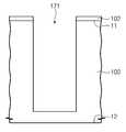
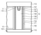
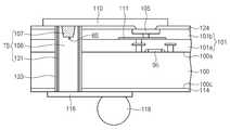
도 1을 참조하면, 반도체 장치(10)는 전기적 신호를 기판(100)을 관통하여 전달하는 도전성 연결부(120)를 포함할 수 있다. 상기 도전성 연결부(120)는 상기 기판(100)을 관통하는 관통 전극(TS)을 포함할 수 있다. 상기 도전성 연결부(120)는 상기 관통 전극(TS)과 접촉되며 상기 기판(100)의 상면(100a) 상에 배치된 상부 배선(110)과, 상기 관통 전극(TS)과 접촉되며 상기 기판(100)의 하면(100c) 상에 배치된 하부 배선(116) 중 적어도 하나를 포함할 수 있다. 상기 상면(100a)은 상기 기판(100)의 활성면으로, 상기 하면(100c)은 상기 기판(100)의 비활성면으로 지칭될 수 있다. 상기 상면(100a) 및 상기 하면(100c) 각각은 기판(100)의 두께 방향과 수직하는 수평 방향으로 연장된 대체로 평평한 면일 수 있다.Referring to FIG. 1, the
상기 상부 배선(110)은 상기 기판(100)의 상면(100a)을 따라 수평하게 연장될 수 있고, 상기 하부 배선(116)은 상기 기판(100)의 하면(100c)을 따라 수평하게 연장될 수 있다. 상기 상부 배선(110)과 상기 하부 배선(116) 중 적어도 어느 하나는 재배선될 수 있다. 상기 하부 배선(116)에는 상기 반도체 장치(10)를 다른 장치, 가령 다른 반도체 장치 혹은 인쇄회로기판에 전기적으로 연결할 수 있는 연결단자로서 제 1 범프(118)가 부착되어 있을 수 있다. 상기 상부 배선(110)에 연결단자가 더 부착될 수 있다.The
상기 관통 전극(TS)은 상기 기판(100)을 수직 관통하여 상기 상부 배선(110) 및 상기 하부 배선(116)과 연결될 수 있다. 상기 상부 배선(110)을 통해 전달되어 오는 전기적 신호는 상기 관통 전극(TS)을 따라 상기 기판(100)을 수직 관통하여 상기 하부 배선(116)으로 혹은 그 역으로 전달될 수 있다.The penetrating electrode TS may vertically penetrate the
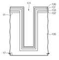
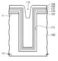
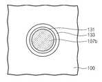
상기 기판(100)의 상면(100a) 및 하면(100c)은 상부 보호막(124) 및 하부 보호막(114)에 의해 각각 덮여질 수 있다. 상기 상부 보호막(124) 및 상기 하부 보호막(114)은 상기 기판(100)을 외부환경으로부터 보호하며 전기적으로 절연시킬 수 있다. 상기 도전성 연결부(120)는 기판(100)과 전기적으로 절연될 수 있다. 예컨대, 상기 상부 보호막(124)은 상기 상부 배선(110)을 상기 기판(100)의 상면(100a)으로부터 이격시켜 전기적으로 절연시키고, 상기 하부 보호막(114)은 상기 하부 배선(116)을 상기 기판(100)의 하면(100c)으로부터 이격시켜 전기적으로 절연시킬 수 있다. 일 예로, 상기 상부 보호막(124) 및 상기 하부 보호막(114)은 실리콘 산화물, 실리콘 질화물, 또는 실리콘 산화질화물을 포함할 수 있다. 상기 관통 전극(TS)은 상기 기판(100)을 관통하는 비아홀(171) 내에 제공될 수 있다. 상기 비아홀(171)은 상기 기판(100)의 내표면에 의하여 정의되는 부분일 수 있다. 상기 관통 전극(TS)은 라이너 절연막(133)에 의하여 상기 기판(100)과 전기적으로 절연될 수 있다. 상기 비아홀(171)은 상기 상면(100a)과 상기 하면(100c)을 잇는 대체로 수직한 면일 수 있다. 상기 라이너 절연막(133)은 산화막 혹은 질화막을 포함할 수 있다. 상기 라이너 절연막(133)은 상기 관통 전극(TS)을 둘러싸며 그 측벽을 따라 상기 상부 배선(110)에서부터 상기 하부 배선(116)까지 연장될 수 있다.The
상기 관통 전극(TS)은 상기 비아홀(171)의 일부를 채우는 금속층(108) 및 상기 비아홀(171) 내에서, 상기 금속층(108) 상에 제공되는 합금층(107)을 포함할 수 있다. 상기 합금층(107)은 상기 기판(100)의 상면(110a)에 인접한 상기 관통 전극(TS)의 상면에 노출되어 상기 상부 배선(110)에 연결될 수 있다. 상기 합금층(107)은 상기 기판(100)의 하면(110c)에 인접한 상기 관통 전극(TS)의 하면에 노출되지 않을 수 있다. 일 예로, 상기 합금층(107)의 상기 상면(110a)에 수직하는 방향으로의 두께(T1)는 상기 관통 전극(TS)의 총 높이(H1)의 약2% 내지 약15%일 수 있다. 상기 관통 전극(TS)은 상기 라이너 절연막(133)과 상기 금속층(108) 사이에 제공되는 배리어층(131)을 포함할 수 있다. 상기 배리어층(131)은 상기 금속층(108)으로부터 금속 원자들이 상기 기판(100)으로 확산하는 것을 줄일 수 있다. 상기 배리어층(131)은 티타늄, 티타늄질화물, 탄탈륨, 탄탈륨질화물, 루테늄, 코발트, 망간, 텅스텐 질화물, 니켈, 니켈붕화물 또는 티타늄/티타늄 질화물과 같은 이중막을 포함할 수 있다.The penetrating electrode TS may include a
상기 금속층(108)은 구리, 텅스텐, 은, 금, 또는 인듐을 포함할 수 있다. 상기 합금층(107)은 상기 금속층(108)에 포함된 금속 원소와 다른 금속 원소를 포함할 수 있다. 일 예로, 상기 합금층(107)은 상기 금속층(108)에 포함된 금속 원소와 다른 금속 원소와, 상기 금속층(108)에 포함된 금속 원소의 합금 물질을 포함할 수 있다. 상기 금속층(108)이 구리인 경우, 상기 합금층(107)은 구리와 다른 금속원소 또는 금속원소들, 일 예로, W, Mn, Cr, Ag, Au, Ni,또는 SgAG 중 적어도 하나를 포함하는 합금일 수 있다. 상기 합금층(107)은 2종 또는 3종 이상의 금속 원소들을 포함하는 합금일 수 있다. 상기 합금층(107)은 비금속 불순물 원소를 더 포함할 수 있다. 일 예로, 상기 구리와 다른 금속원소를 포함하는 합금 물질은 Cu-Mn합금(Mn은 5atm% 내지 8atm%), Cu-Au합금(Au는 10atm%이상), Cu-Ni합금(Ni는 2atm%이상) 등일 수 있다. 일 예로, 상기 금속층(108)이 텅스텐인 경우, 상기 합금층(107)은 텅스텐과 다른 금속원소를 포함하는 합금일 수 있다. 일 예로, 상기 텅스텐과 다른 금속원소를 포함하는 합금 물질은 W-Mn합금(Mn은 5atm% 내지 8atm%), W-Au합금(Au는 10atm%이상), W-Ni합금(Ni는 2atm%이상) 등일 수 있다.The
상기 금속층(108)은 합금이 아닐 수 있다. 본 명세서에서, 합금은 금속들 간의 화합물에 한정되며, 금속과 비금속 간의 화합물을 포함되지 않는 것으로 기술된다. 상기 금속간의 화합물은 비금속 물질을 더 포함할 수 있다.The
상기 합금층(107)은 상기 금속층(108)에 포함된 금속 원소를 포함하지 않을 수 있다. 일 예로, 상기 금속층(108)이 구리인 경우, 상기 합금층(107)은 구리를 포함하지 않는 합금 물질로 형성될 수 있다. 일 예로, 상기 구리를 포함하지 않는 합금 물질은 Ag-Ni합금, Ag-Mn합금, Ag-Au합금, W-Ni합금, W-Mn합금, W-Au합금, W-Ti합금, 또는 W-Ta합금 중 적어도 하나를 포함할 수 있다.The
상기 합금층(107)은 이후 수행되는 고온 공정에 의하여 상기 금속층(108)의 결정립 사이즈가 증가되는 것을 방지할 수 있다. 일 예로, 상기 고온 공정은 상기 관통 전극(TS)의 형성 이후 수행되는 금속 배선의 형성 공정일 수 있다. 일 예로 상기 고온 공정은 약 400℃이상일 수 있다. 상기 금속층(108)의 결정립들은 고온 공정에서 입계(grain boundary)의 이동에 의하여 상대적으로 작은 결정립들은 소멸되고 큰 결정립들은 계속 성장될 수 있다. 그 결과, 상기 기판(100)의 상면(100a)에 인접한 상기 관통 전극(TS)의 상면의 결정립들은 열적 스트레스(thermal stress)에 의하여 국부적으로 돌출(extrusion)될 수 있다. 상기 돌출 현상은 상기 관통 전극(TS)과 상기 관통 전극(TS) 상의 금속 배선(일 예로, 상기 상부 배선(110)) 사이의 단선 또는 접촉 저항 불량을 발생시키거나, 상기 관통 전극(TS) 상의 절연막의 크랙을 유발할 수 있다.The
상기 금속층(108) 상에 상기 합금층(107)을 제공하는 경우, 상기 관통 전극(TS)과 상기 상부 배선(110)이 접촉하는 부분에서 상기 관통 전극(TS)의 결정립 성장이 억제될 수 있다. 일 예로, 도 1에 도시된 바와 같이, 상기 금속층(108)이 상기 합금층(107) 아래의 바디부(BD)와 상기 합금층(107)과 상기 배리어층(131) 사이의 연장부(EX)를 포함하는 경우, 상기 연장부(EX)의 결정립 성장은 상기 바디부(BD)의 결정립 성장에 비하여 억제될 수 있다. 즉, 상기 고온 공정 이후, 상기 연장부(EX)의 결정립 크기는 상기 바디부(BD)의 결정립 크기에 비하여 작을 수 있다.When the
상기 합금층(107)은 상기 합금층(107)에 포함된 이종 금속 원소에 의하여 결정립 성장이 억제될 수 있다. 일 예로, 상기 합금층(107)의 평균 결정립 크기는 상기 바디부(BD)의 평균 결정립 크기의 1/2배 이하일 수 있다. 일 예로, 상기 바디부(BD)의 평균 결정립 크기는 약3㎛∼약4㎛일 수 있고, 상기 합금층(107)의 평균 결정립 크기는 약1㎛∼ 약2㎛일 수 있다.The
상기 합금층(107)은 상기 금속층(108)의 결정립 성장에 의한 돌출 현상을 완화하고, 상기 관통 전극(TS)과 상기 상부 배선(110) 사이의 접촉 저항을 개선할 수 있다.The
상기 반도체 장치(10)에 있어서 상기 금속층(108) 및 상기 합금층(107)의 형태나 구조는 후술할 실시예들을 참조하여 다양하게 변형될 수 있다. 또한, 상기 라이너 절연막(133), 상기 배리어층(131) 및 상기 비아홀(171)의 형태는 다양하게 변형될 수 있다.The shape and structure of the
<방법예><Example of method>
도 2 내지 도 7b는 본 발명의 일 실시예에 따른 반도체 장치의 제조방법을 도시한 단면도들 및 평면도이다.FIGS. 2 to 7B are cross-sectional views and plan views illustrating a method of manufacturing a semiconductor device according to an embodiment of the present invention.
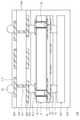
도 2를 참조하면, 기판(100)이 제공될 수 있다. 기판(100)은 실리콘 혹은 실리콘을 포함하는 반도체를 포함할 수 있다. 상기 기판(100)의 제 1 면(11) 상에 상부 절연막(102)이 형성될 수 있다. 일 예로, 상기 상부 절연막(102)은 실리콘 산화물, 실리콘 질화물 또는 실리콘 산화질화물을 포함할 수 있다. 상기 상부 절연막(102)을 관통하고 상기 기판(100)의 제 2 면(12) 방향으로 연장되는 비아홀(171)이 형성될 수 있다. 상기 제 1 면(11)은 기판의 활성면으로, 상기 제 2 면(12)은 상기 기판의 비활성면으로 지칭될 수 있다. 평면적 관점에서, 상기 비아홀(171)은 원형, 타원형 또는 사각형일 수 있다. 상기 비아홀(171)은 드릴링 방법, 보쉬(Bosch) 에칭, 또는 스테디(Steady State) 에칭 방법으로 형성될 수 있다. 상기 비아홀(171)은 상기 기판(100)을 관통하지 않는 깊이까지 연장될 수 있다. 일 예로, 상기 비아홀(171)의 깊이는 대략 50㎛ 이상 일 수 있다. 상기 비아홀(171)의 깊이는 디자인 룰 (Design Rule)이나 소자 요구 특성에 의해 변화될 수 있다.Referring to FIG. 2, a
도 3을 참조하면, 상기 비아홀(171) 내에 라이너 절연막(133)이 형성될 수 있다. 상기 라이너 절연막(133)은 산화막(예: SiOx)이나 질화막(예: SiNx)과 같은 절연성 물질을 증착하여 형성할 수 있다. 상기 라이너 절연막(133)은 비아홀(171)의 내벽을 따라 실질적으로 콘포말하게 증착될 수 있다. 상기 라이너 절연막(133)은 상기 상부 절연막(102) 상으로 연장되도록 형성될 수 있다. 일 예로, 상기 라이너 절연막(133)의 형성은 화학 기상 증착(Chemical Vapor Deposition: CVD)에 의하여 형성될 수 있다.Referring to FIG. 3, a
상기 라이너 절연막(133) 상에 배리어층(131)이 형성될 수 있다. 상기 배리어층(131)은 티타늄, 티타늄질화물, 탄탈륨, 탄탈륨질화물, 루테늄, 코발트, 망간, 텅스텐 질화물, 니켈, 니켈붕화물 또는 티타늄/티타늄 질화물과 같은 이중막을 포함할 수 있다. 일 예로, 상기 배리어층(131)은 스퍼터링, CVD 또는 원자층 증착(Atomic Layer DepositionL ALD)에 의하여 형성될 수 있다.A
상기 배리어층(131) 상에 시드층(seed layer, 106)이 형성될 수 있다. 상기 시드층(106)은 이하 설명될 금속층의 증착을 위한 층으로, 상기 금속층과 동일한 물질을 포함할 수 있다. 상기 시드층(106)은 구리, 텅스텐, 은, 금, 또는 인듐을 포함할 수 있다. 일 예로, 상기 시드층(106)은 스퍼터링 방법에 의하여 형성될 수 있다.A
도 4를 참조하면, 상기 시드층(106) 상에 금속층(108)이 형성될 수 있다. 일 예로, 상기 금속층(108)은 구리, 텅스텐, 은, 금, 또는 인듐으로 형성될 수 있다. 상기 금속층(108)은 상기 시드층(106)을 이용한 전해도금 공정으로 형성될 수 있다. 다른 실시예에서, 상기 금속층(108)은 무전해도금 또는 스퍼터링으로 형성될 수 있다. 상기 금속층(108)은 상기 시드층(106)을 따라서 상기 상부 절연막(102) 상으로 연장되도록 형성될 수 있다. 일 예로, 상기 전해도금 공정은 CuSO4, H2SO4, 및 Cl을 포함하는 전해 용액에 웨이퍼를 담구어 수행될 수 있다. 상기 금속층(108)은 상기 비아홀(171)을 완전히 채우지 않도록 형성될 수 있고, 그 결과, 상기 금속층(108)의 상부에 상기 금속층(108)의 측벽에 의하여 정의되는 홀 영역(172)이 형성될 수 있다. 일 예로, 상기 금속층(108)은 상기 비아홀(171)의 하면보다 상기 비아홀(171)의 측벽 상에 상대적을 얇게 형성될 수 있다. 이와 같은 상기 금속층(108)의 두께 조절은 전해도금 공정에 사용되는 서프레서(suppressor) 및 액설러레이터(accelerator)의 조절 또는 전류 밀도 분포 조절에 의하여 달성될 수 있다. 일 예로, 상기 서프레서는 PEG (Poly Ethylene Glycol)를 포함할 수 있고, 상기 액설러레이터는 SPS (Sulfopropyl Disulfide) 또는 Bis-(3-sulfopropyl) disulfide를 포함할 수 있다. 상기 서프레서는 상기 비아홀(171)의 측벽 상에 상기 금속층(108)이 형성되는 것을 억제할 수 있다.Referring to FIG. 4, a
도 5를 참조하면, 상기 홀 영역(172)을 채우는 합금층(107)이 형성될 수 있다. 일 예로, 상기 합금층(107)은 이미 형성된 상기 합금층(107)을 전류 의 공급 통로로 사용하여 전해 도금 공정으로 형성될 수 있다. 다른 실시예에 있어서, 상기 합금층(107)의 형성은 무전해 도금, 또는 스퍼터링으로 형성될 수 있다. 상기 합금층(107)은 상기 금속층(108)을 따라서 상기 상부 절연막(102) 상으로 연장되도록 형성될 수 있다. 상기 합금층(107)은 상기 금속층(108)에 포함된 금속 원소와 다른 금속 원소를 포함하는 물질로 형성될 수 있다. 일 예로, 상기 합금층(107)은 상기 금속층(108)에 포함된 금속 원소와 다른 금속 원소와, 상기 합금층(107)은 상기 금속층(108)에 포함된 금속 원소의 합금으로 형성될 수 있다. 일 예로, 상기 금속층(108)이 구리인 경우, 상기 합금층(107)은 구리와 다른 금속원소 또는 금속원소들, 일 예로, W, Mn, Cr, Ag, Au, Ni,또는 SgAG 중 적어도 하나를 포함하는 합금일 수 있다. 상기 합금층(107)은 2종 또는 3종 이상의 금속 원소들을 포함하는 합금일 수 있다. 상기 합금층(107)은 비금속 불순물 원소를 더 포함할 수 있다. 일 예로, 상기 구리와 다른 금속원소를 포함하는 합금 물질은 Cu-Mn합금(Mn은 5atm% 내지 8atm%), Cu-Au합금(Au는 10atm%이상), Cu-Ni합금(Ni는 2atm%이상) 등일 수 있다. 일 예로, 상기 금속층(108)이 텅스텐인 경우, 상기 합금층(107)은 텅스텐과 다른 금속원소를 포함하는 합금일 수 있다. 일 예로, 상기 텅스텐과 다른 금속원소를 포함하는 합금 물질은 W-Mn합금(Mn은 5atm% 내지 8atm%), W-Au합금(Au는 10atm%이상), W-Ni합금(Ni는 2atm%이상) 등일 수 있다. 이와 같은 상기 합금층(107)의 형성은 전해 용액 내에 상기 합금층(107)을 구성하는 금속 원소의 공급원을 추가하여 수행될 수 있다. 상기 합금층(107)의 형성 후, 어닐링 공정이 수행될 수 있다. 상기 어닐링 공정은 약 200℃ 내지 약 500℃ 에서 수행될 수 있다. 상기 어닐링 공정에 의하여 상기 금속층(108) 내의 결정립들이 일부 성장될 수 있으며, 상기 금속층(108)과 상기 합금층(107) 내의 잔류 응력이 완화될 수 있다.Referring to FIG. 5, an
상기 합금층(107)은 상기 금속층(108)에 포함된 금속 원소를 포함하지 않는 합금으로 형성될 수 있다. 일 예로, 상기 금속층(108)이 구리인 경우, 상기 합금층(107)은 구리를 포함하지 않는 합금 물질로 형성될 수 있다. 일 예로, 상기 구리를 포함하지 않는 합금 물질은 Ag-Ni합금, Ag-Mn합금, Ag-Au합금, W-Ni합금, W-Mn합금, W-Au합금, W-Ti합금, 또는 W-Ta합금 중 적어도 하나를 포함할 수 있다.The
도 6을 참조하면, 평탄화 공정을 수행하여 상기 상부 절연막(102) 상의 층들이 제거될 수 있다. 일 예로, 상기 평탄화 공정은 화학적 물리적 연막(Chemical Mechanical Polishing: CMP)을 포함할 수 있다. 상기 평탄화 공정에 의하여, 상기 비아홀(171) 내에 한정된 관통 전극(TS)이 형성될 수 있다.Referring to FIG. 6, layers on the upper insulating
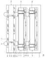
도 7a 및 도 7b를 참조하면, 상기 기판(100)의 제 2 면(12)이 연마되어 상기 관통 전극(TS)이 노출될 수 있다. 도 7b는 도 7a의 상기 관통 전극(TS)의 상면을 도시하는 평면도이다. 상기 연마 공정이 보다 상세하게 설명된다.Referring to FIGS. 7A and 7B, the
먼저, 상기 기판(100)의 제 1 면(11) 상에, 접착층을 이용하여, 캐리어 기판(carrier substrate, 미도시)이 부착될 수 있다. 상기 캐리어 기판은 상기 기판(100)의 상기 제 2 면(12)을 연마하는 과정에서 상기 기판(100)에 작용하는 기계적인 스트레스를 완화하고, 연마 공정 이후에 박형화된 상기 기판(100)에서 발생하는 휨을 방지할 수 있다. 상기 캐리어 기판은 유리기판, 또는 수지기판을 포함할 수 있다. 상기 접착층은 자외선 접착제 또는 열가소성 접착제를 포함할 수 있다. 다음으로, 상기 라이너 절연막(133)이 노출되도록, 상기 기판(100)의 상기 제 2 면(12)이 연마된다. 상기 기판(100)을 연마하는 것은, 예를 들어, CMP, Etch-back, Spin Etch 방법을 각각 또는 혼용하는 그라인딩(grinding) 방법을 이용하여 수행될 수 있다.First, a carrier substrate (not shown) may be attached to the
다음으로, 상기 관통 전극(TS)이 상기 기판(100)의 상기 제 2 면(12)으로부터 돌출되도록, 상기 기판(100)이 선택적으로 식각될 수 있다. 상기 선택적 식각은 상기 라이너 절연막(133)에 비하여 큰 식각 선택비를 갖는 습식 식각 또는 건식 식각 공정을 이용하여 상기 기판(100)을 선택적으로 식각하는 것일 수 있다. 예를 들어, 상기 라이너 절연막(133)이 실리콘 산화막일 경우, SF6 식각 가스를 이용하여 상기 기판(100)이 선택적으로 식각될 수 있다. 상기 제 2 면(12) 상에 상기 관통 전극(TS)을 덮는 하부 절연막(103)이 형성된 후, 상기 관통 전극(TS)이 노출되도록 상기 하부 절연막(103)의 일부를 제거할 수 있다. 상기 하부 절연막(103)은 실리콘 산화막, 실리콘 질화막 또는 실리콘 산화질화막일 수 있다.Next, the
상기 기판(100)의 제 1 면(11) 상에 상기 관통 전극(TS)과 연결되는 상부 배선(110)이 형성될 수 있다. 상기 기판(100)의 제 2 면(12) 상에 상기 관통 전극(TS)과 연결되는 하부 배선(116)이 형성될 수 있다. 일 예로, 상기 상부 배선(110)과 상기 하부 배선(116)은 구리, 텅스텐, 은, 금, 또는 인듐 을 포함하는 물질로 형성될 수 있다. 상기 상부 배선(110) 및 상기 하부 배선(116)의 위치, 상기 관통 전극(TS)과의 관계는 이하 설명될 관통 전극의 형성 순서에 따라 변경될 수 있다.An
본 발명의 일 실시예에 따른 관통 전극(TS)은 상기 비아홀(171)의 일부를 채우는 상기 금속층(108) 및 상기 금속층(108) 상의 상기 합금층(107)을 포함할 수 있다. 상기 합금층(107)은 상기 금속층(108)의 상면에 의해 정의된 홀 영역(172) 내에 제공될 수 있다. 상기 금속층(108)은 상기 합금층(107)과 상기 배리어층(131) 사이로 연장될 수 있다. 상기 관통 전극(TS)의 상면에는 상기 합금층(107)이 노출되고, 상기 합금층(107) 주위로 차례로 형성된 상기 금속층(108), 상기 시드층(106), 상기 배리어층(131), 및 상기 라이너 절연막(133)이 노출된다. 상기 합금층(107) 상면의 직경(d1)은 상기 연장부의 두께(d2)보다 클 수 있다. 다른 실시예에서, 상기 합금층(107) 상면의 직경(d1)은 상기 연장부의 두께(d2)보다 작을 수 있다.The penetrating electrode TS according to an embodiment of the present invention may include the
상기 홀 영역(172)의 측벽은 수직이 아닌 경사를 갖는 것으로 도시되었으나, 이와는 달리 상기 기판(100)의 제 1 면(11) 및/또는 제 2 면(12)과 실질적으로 수직일 수 있다.The sidewalls of the
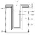
도 8a 및 도 8b는 본 발명의 다른 실시예에 따른 관통 전극의 형상을 도시하는 단면도 및 평면도이다. 설명의 간략화를 위하여 동일한 구성에 대한 설명은 생략된다. 본 실시예에 있어서, 상기 관통 전극(TS)은 상기 금속층(108)과 상기 합금층(107) 사이에 분리 도전층(109)을 더 포함할 수 있다. 상기 분리 도전층(109)은 상기 금속층(108)과 상기 합금층(107)을 분리할 수 있다. 상기 분리 도전층(109)은 상기 금속층(108)과 상기 합금층(107)이 서로 다른 공정에 의하여 형성되는 경우 제공될 수 있다. 일 예로, 상기 분리 도전층(109)은 티타늄, 티타늄질화물, 탄탈륨, 탄탈륨질화물, 루테늄, 코발트, 망간, 텅스텐 질화물, 니켈, 니켈붕화물 또는 티타늄/티타늄 질화물과 같은 이중막을 포함할 수 있다. 상기 분리 도전층(109)은 상기 합금층(107)과 상기 금속층(108) 사이로 연장되어 상기 관통 전극(TS)의 상면에 노출될 수 있다. 상기 분리 도전층(109)은 본 실시예에 한정되지 않으며, 이후 설명될 다른 실시예들에 추가될 수 있다.8A and 8B are a cross-sectional view and a plan view showing the shape of a penetrating electrode according to another embodiment of the present invention. Description of the same configuration is omitted for the sake of simplicity. In the present embodiment, the penetrating electrode TS may further include a separate
도 9a, 도 9b, 및 도 9c는 본 발명의 또 다른 실시예에 따른 관통 전극의 형상을 도시하는 단면도들 및 평면도이다. 설명의 간략화를 위하여 동일한 구성에 대한 설명은 생략된다. 본 실시예에 있어서, 합금층(107a)은 시드층(106)과 접하고, 상기 금속층(108)은 관통 전극(TS)의 상면에 노출되지 않을 수 있다. 즉, 상기 합금층(107a)은 상기 시드층(106)의 측벽을 노출하는 홀 영역(173) 내에 제공될 수 있다. 상기 합금층(107a)의 형상은 도 9c에 도시된 바와 같이 금속층(108a)이 상기 시드층(106)의 일부를 노출하도록 형성함에 따라 결정될 수 있다. 이와 같은 상기 금속층(108a)의 형상은 전해 도금 공정 시 상기 시드층(106)에 인가되는 전류를 중지하여 상기 시드층(106)의 측벽 상에 형성된 금속층의 일부를 용해시켜 형성될 수 있다. 예를 들면, 구체적으로 상기 금속층(108a)의 상부가 형성될 때에, 전해 도금 공정에 사용되는 서프레서(suppressor)를 상대적으로 강하게 조절하여 상기 시드층(106)의 상부 측벽에는 도금이 되지 않도록 조절할 수 있다.9A, 9B and 9C are cross-sectional views and plan views showing the shape of a penetrating electrode according to another embodiment of the present invention. Description of the same configuration is omitted for the sake of simplicity. In this embodiment, the
도 10a, 도 10b, 및 도 10c는 본 발명의 또 다른 실시예에 따른 관통 전극의 형상을 도시하는 단면도들 및 평면도이다. 설명의 간략화를 위하여 동일한 구성에 대한 설명은 생략된다. 본 실시예에 있어서, 합금층(107b)은 배리어층(131)과 접하고, 금속층(108a) 및 시드층(106a)은 관통 전극(TS)의 상면에 노출되지 않을 수 있다. 즉, 상기 합금층(107b)은 상기 배리어층(131)의 측벽을 노출하는 홀 영역(174) 내에 제공될 수 있다. 상기 합금층(107a)의 형상은 도 10c에 도시된 바와 같이 상기 금속층(108a) 및 상기 시드층(106a)이 상기 배리어층(131)의 일부를 노출하도록 형성함에 따라 결정될 수 있다. 이와 같은 상기 금속층(108a) 및 상기 시드층(106a)의 형상은 전해 도금 공정 시 상기 시드층(106a)에 인가되는 전류를 중지하여 상기 시드층(106)의 측벽 상에 형성된 금속층 및 상기 시드층(106)층의 일부를 용해시켜 형성될 수 있다. 이 때, 상기 금속층(108a) 상의 상기 합금층(107b)은 도금 방식이 아닌 CVD 방식 또는 PVD 방식으로 합금층을 형성한 후, 열처리를 통하여 리플로우(Reflow) 하는 방식으로 형성될 수 있다.10A, 10B and 10C are cross-sectional views and plan views showing the shape of a penetrating electrode according to another embodiment of the present invention. Description of the same configuration is omitted for the sake of simplicity. In the present embodiment, the
상술한 관통 전극 및 그 제조 방법은 관통 전극을 포함하는 반도체 장치의 다양한 형성 방법들에 각각 적용될 수 있다. 관통 전극은 비아 라스트(Via Last), 비아 미들(Via Middle) 및 비아 퍼스트(Via First) 구조들 중 어느 하나로 분류될 수 있다. 이하, 상기 각 구조들 및 형성 방법에 대하여 보다 자세히 설명된다.The above-described penetrating electrode and its manufacturing method can be applied to various forming methods of the semiconductor device including the penetrating electrode, respectively. The penetrating electrode can be classified into any one of Via Last, Via Middle, and Via First structures. Hereinafter, each of the structures and the forming method will be described in detail.
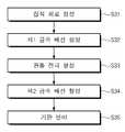
<Via Middle><Via Middle>
도 11a는 관통 전극의 형성이 집적 회로의 형성과 금속 배선들의 형성 사이에 수행되는 비아 미들 구조의 제조 방법의 공정 흐름도이다. 도 11b는 도 11a에 의해 형성된 반도체 장치의 단면도이다. 설명의 간소화를 위하여 관통 전극은 도 7a 및 도 7b를 참조하여 설명된 실시예의 형상으로 도시되었으나, 이에 한정되지 않으며 다른 실시예에 따른 관통 전극의 형상 또한 적용될 수 있다. 설명의 간소화를 위하여 동일한 구성에 대한 설명은 생략될 수 있다.11A is a process flow chart of a manufacturing method of a via-amide structure in which formation of a penetrating electrode is performed between formation of an integrated circuit and formation of metal wirings. 11B is a cross-sectional view of the semiconductor device formed by Fig. For the sake of simplicity, the through electrodes are shown in the form of the embodiment described with reference to Figs. 7A and 7B, but the present invention is not limited thereto, and the shape of the penetrating electrode according to another embodiment can also be applied. Description of the same configuration may be omitted for simplification of description.
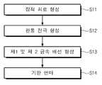
도 11a 및 도 11b를 참조하면, 관통 전극(TS)의 형성(S12)은 집적 회로(95)의 형성(S11) 이후에, 그리고 제 1 및 제 2 금속 배선(상부 배선(110) 및 금속 배선(111))이 형성(S14) 되기 이전에 수행될 수 있다. 상기 관통 전극(TS)의 형성(S12) 이후, 도 7a 및 도 7b를 참조하여 설명된 기판 연마(S13)가 수행되고, 그 후, 상기 상부 배선(110) 및 상기 금속 배선(111)이 형성될 수 있다.11A and 11B, formation of the penetrating electrode TS (S12) is performed after the formation of the integrated circuit 95 (S11) and after the formation of the first and second metal wirings (the
층간 절연막(101)은 기판(100)의 상면(100a) 상에 형성되어 상기 집적 회로(95)를 덮는 제 1 층간 절연막(101a)과, 상기 제 1 층간 절연막(101a) 상에 형성되어 상기 상부 배선(110) 및 상기 금속 배선(111)을 덮는 제 2 층간 절연막(101b)을 포함할 수 있다. 상기 상부 배선(110)은 상기 제 1 층간 절연막(101a)과 상기 제 2 층간 절연막(101b) 사이에 제공되어, 상기 관통 전극(TS)과 상기 집적 회로(95)를 전기적으로 연결할 수 있다. 상기 금속 배선(111)은 상기 상부 배선(110) 상에 제공되고, 상기 상부 배선(110)과 상기 제 2 층간 절연막(101b)의 상부에 형성된 본딩패드(105)를 연결할 수 있다. 관통 전극(TS)은 기판(100)과 제 1 층간 절연막(101a)을 관통할 수 있다. 상부 보호막(124)은 제 2 층간 절연막(101b) 상에 형성될 수 있고, 금속 배선(111)에 연결된 상기 본딩패드(105)를 개방시킬 수 있다.The
본 실시예에서, 상기 관통 전극(TS)은 상기 기판(100)의 상면(100a)에 대향하는, 상기 제 1 층간 절연막(101a)의 상면으로 연장되어 상기 상부 배선(110)에 연결된다. 상기 관통 전극(TS)을 구성하는 합금층(107)의 하면(BS)은 상기 기판(100)의 상면(100a)보다 높을 수 있다.The penetrating electrode TS extends to the upper surface of the first
<Via First><Via First>
도 12a는 관통 전극이 집적 회로와 배선들의 형성 이전에 형성되는 비아 퍼스트 구조의 제조 방법의 공정 흐름도이다. 도 12b는 도 12a에 의해 형성된 반도체 장치의 단면도이다. 설명의 간소화를 위하여 동일한 구성에 대한 설명은 생략될 수 있다.12A is a process flow diagram of a fabrication method of a via-first structure in which the penetrating electrode is formed before the formation of the integrated circuit and the wirings. 12B is a cross-sectional view of the semiconductor device formed by FIG. 12A. Description of the same configuration may be omitted for simplification of description.
도 12a 및 도 12b를 참조하면, 관통 전극(TS)의 형성(S21)은 집적 회로(95)의 형성(S22) 이전에 수행될 수 있다. 보다 상세하게, 상기 관통 전극(TS)의 형성(S21) 이후, 집적 회로(95)가 형성되고(S22), 제 1 및 제 2 금속 배선(상부 배선(110) 및 금속 배선(111))이 형성(S23)될 수 있다. 그 후, 도 7a 및 도 7b를 참조하여 설명된 기판 연마(S24)가 수행될 수 있다.12A and 12B, the formation of the penetrating electrode TS (S21) may be performed before the formation of the integrated circuit 95 (S22). More specifically, after the formation of the penetrating electrode TS (S21), the
상기 기판(100)의 상면(100a)에는 층간 절연막(101)이 형성될 수 있다. 상기 층간 절연막(101)은 상기 집적 회로(95)와 상부 배선(110)을 덮는 제 1 층간 절연막(101a)과, 제 1 층간 절연막(101a) 상에 형성된 금속 배선(111)을 덮고 본딩패드(105)를 노출시키는 제 2 층간 절연막(101b)을 포함할 수 있다. 상기 상부 배선(110)은 제 1 금속 배선(M1), 상기 금속 배선(111)은 제 2 금속 배선(M2)으로 불리울 수 있다.An interlayer insulating
본 실시예에서, 상기 제 1 층간 절연막(101a)은 상기 관통 전극(TS)의 상면을 덮을 수 있다. 상기 상부 배선(110)은 상기 제 1 층간 절연막(101a)과 상기 관통 전극(TS) 사이에 제공될 수 있다. 상기 금속 배선(111)은 상기 제 1 층간 절연막(101a)과 상기 제 2 층간 절연막(101b) 사이에 제공되어 상기 상부 배선(110)과 상기 집적 회로(95)를 전기적으로 연결할 수 있다. 상기 관통 전극(TS)은 상기 상부 배선(110) 아래에 제공된 식각 방지층(115)을 관통하여 상기 상부 배선(110)과 연결될 수 있다.In the present embodiment, the first
상기 관통 전극(TS)을 구성하는 합금층(107)의 하면(BS)은 상기 기판(100)의 상면(100a)보다 낮을 수 있다.The lower surface BS of the
<Via Last><Via Last>
도 13a는 관통 전극이 집적 회로 형성 이후, 및 제 1 금속 배선과 제 2 금속 배선의 형성 사이에 형성되는 비아 라스트 구조의 제조 방법의 공정 흐름도이다. 도 13b는 도 13a에 의해 형성된 반도체 장치의 단면도이다. 설명의 간소화를 위하여 동일한 구성에 대한 설명은 생략될 수 있다.13A is a process flow chart of a method of manufacturing a via-via structure in which a through electrode is formed after the formation of an integrated circuit and between the formation of a first metal interconnection and a second metal interconnection. 13B is a cross-sectional view of the semiconductor device formed by Fig. Description of the same configuration may be omitted for simplification of description.
도 13 및 도 13b를 참조하면, 관통 전극(TS)의 형성(S33)은 집적 회로(95)의 형성(S31) 및 제 1 금속 배선(금속 배선(111))의 형성 이후에 수행될 수 있다. 보다 상세하게, 상기 집적 회로(95)의 형성(S31) 이후, 상기 집적 회로(95)를 덮는 제 1 층간 절연막(101a)이 형성될 수 있다. 상기 제 1 층간 절연막(101a) 상에 금속 배선(111)을 형성 후, 상기 금속 배선(111)을 덮는 제 2 층간 절연막(101b)이 형성될 수 있다. 상기 제 1 및 제 2 층간 절연막들(101a, 101b)을 관통하는 상기 관통 전극(TS)이 형성된 후(S33), 상기 관통 전극(TS)과 상기 집적 회로(95)를 전기적으로 연결하는 제 2 금속 배선(상부 배선(110))이 형성될 수 있다. 즉, 상기 관통 전극(TS)은 상기 제 1 및 제 2 층간 절연막들(101a, 101b)을 형성한 후에 형성될 수 있다. 상기 금속 배선(111)은 제 1 금속 배선(M1)으로, 상기 상부 배선(110)은 제 2 금속 배선(M2)으로 불리울 수 있다. 그 후, 도 7a 및 도 7b를 참조하여 설명된 기판 연마(S35)가 수행될 수 있다.13 and 13B, formation (S33) of the penetrating electrode TS can be performed after the formation of the integrated circuit 95 (S31) and the formation of the first metal wiring (metal wiring 111) . More specifically, after the formation of the integrated circuit 95 (S31), a first
본 실시예에서, 상기 관통 전극(TS)은 상기 제 1 층간 절연막(101a)에 대향하는, 상기 제 2 층간 절연막(101b)의 상면으로 연장될 수 있다. 상기 관통 전극(TS)을 구성하는 합금층(107)의 하면(BS)은 상기 제 1 층간 절연막(101a)의 상면보다 높을 수 있다.In this embodiment, the penetrating electrode TS may extend to the upper surface of the second
<응용예><Application example>
도 14 내지 도 16은 본 발명의 실시예들에 따른 반도체 패키지들의 단면도들이다.14 to 16 are sectional views of semiconductor packages according to embodiments of the present invention.
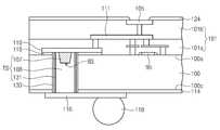
도 14를 참조하여, 본 발명의 실시예들에 따른 반도체 패키지(401)의 일 예는 패키지 기판(200)과 그 위에 실장된 반도체 장치(10)를 포함할 수 있다. 상기 패키지 기판(200)은 인쇄회로 기판일 수 있다. 상기 패키지 기판(200)은 절연 기판(201), 상기 절연 기판(201)을 관통하는 패키지 기판 관통 비아(207), 상기 절연 기판(201)의 상하면에 배치되는 도전 패턴들(209, 211) 및 상기 도전 패턴들(209, 211)을 일부 덮는 패키지 기판 절연막들(205, 203)을 포함할 수 있다. 상기 반도체 장치(10)는 도 1 내지 도 13을 참조하여 설명된 반도체 장치에 대응될 수 있다.14, an example of a
상기 반도체 장치(10)는, 상기 기판(100)의 제 2 면(12)이 상기 패키지 기판(200)에 마주보도록, 상기 패키지 기판(200) 상에 실장될 수 있다. 즉, 상기 반도체 장치(10)는 제 1 범프(118)에 의해 상기 패키지 기판(200)에 전기적으로 연결될 수 있다. 상기 패키지 기판(200)의 하부에는 제 2 범프(73)가 부착될 수 있다. 상기 범프들(118, 73)은 솔더볼, 도전성 범프, 도전성 스페이서, 핀 그리드 어레이 또는 이들의 조합일 수 있다. 상기 반도체 패키지(401)는 상기 반도체 장치(10)를 덮는 몰드막(310)을 더 포함할 수 있다. 상기 몰드막(310)은 에폭시 몰딩 컴파운드를 포함할 수 있다.The
도 15를 참조하여, 본 발명의 실시예들에 따른 반도체 패키지(402)의 다른 예는 패키지 기판(200)과 그 위에 실장된 제 1 반도체 장치(10)와, 상기 제 1 반도체 장치(10) 상의 제 2 반도체 장치(300)를 포함한다. 상기 패키지 기판(200)은 인쇄회로 기판일 수 있다. 상기 패키지 기판(200)은 절연 기판(201), 상기 절연 기판(201)을 관통하는 패키지 기판 관통 비아(207), 상기 절연 기판(201)의 상하면에 배치되는 도전 패턴들(209, 211) 및 상기 도전 패턴들(209, 211)을 일부 덮는 패키지 기판 절연막들(205, 203)을 포함할 수 있다. 상기 제 1 반도체 장치(10)는 도 1 내지 도 13을 참조하여 설명된 반도체 장치에 대응될 수 있다. 상기 제 2 반도체 장치(300)는 상기 제 1 반도체 장치(10)와는 다른 반도체 장치로, 메모리 칩이나 로직 칩에 대응될 수 있다. 상기 제 2 반도체 장치(300)는 상기 관통 전극을 포함하지 않을 수 있다.15, another example of the
상기 제 1 반도체 장치(10)는 제 1 범프(118)에 의해 상기 패키지 기판(200)에 전기적으로 연결될 수 있다. 상기 제 1 반도체 장치(10)는 상부 배선(110)과 전기적으로 연결된 재배선 구조를 포함할 수 있다. 상기 재배선 구조는 콘택(66) 및 접속 패드(67)을 포함할 수 있다. 상기 제 2 반도체 장치(300)는 상기 제 1 반도체 장치(10)에 플립 칩 본딩 방식으로 실장될 수 있다. 상기 제 2 반도체 장치(300)는 제 3 범프(75)에 의해 상기 제 1 반도체 장치(10)의 접속 패드(67)에 연결될 수 있다. 상기 제 1 반도체 장치(10)는 인터포저의 기능을 할 수 있다. 상기 제 3 범프(75) 및 관통 전극(TS)은 복수 개일 수 있다.The
상기 패키지 기판(200)의 하부에는 제 2 범프(73)가 부착될 수 있다. 상기 범프들(118, 73, 75)은 솔더볼, 도전성 범프, 도전성 스페이서, 핀 그리드 어레이 또는 이들의 조합일 수 있다. 상기 반도체 패키지(402)는 상기 제 1 및 제 2 반도체 장치들(10, 300)을 덮는 몰드막(310)을 더 포함할 수 있다. 상기 몰드막(310)은 에폭시 몰딩 컴파운드를 포함할 수 있다.A second bump (73) may be attached to the bottom of the package substrate (200). The
도 16을 참조하여, 본 발명의 실시예들에 따른 반도체 패키지(403)의 또 다른 예는 패키지 기판(200)과 그 위에 실장된 제 1 반도체 장치(10)와 제 2 반도체 장치(20)를 포함한다. 본 발명의 실시예들에 따른 반도체 패키지(403)는 멀티 칩 패키지일 수 있다. 상기 제 1 반도체 장치(10)와 제 2 반도체 장치(20)는 동일한 종류 및 구조를 가질 수 있다.16, another example of the
상기 패키지 기판(200)은 인쇄회로 기판일 수 있다. 상기 패키지 기판(200)은 절연 기판(201), 상기 절연 기판(201)을 관통하는 패키지 기판 관통 비아(207), 상기 절연 기판(201)의 상하면에 배치되는 도전 패턴들(209, 211) 및 상기 도전 패턴들(209, 211)을 일부 덮는 패키지 기판 절연막들(205, 203)을 포함할 수 있다. 상기 제 1 및 제 2 반도체 장치들(10, 20)은 도 1 내지 도 13을 참조하여 설명된 반도체 장치에 대응될 수 있다.The
상기 제 1 반도체 장치(10) 및 상기 제 2 반도체 장치(20)는 각각 제 1 관통 전극(TS1) 및 제 2 관통 전극(TS2)을 포함할 수 있다. 상기 제 1 관통 전극(TS1)과 상기 제 2 관통 전극(TS2)은 서로 중첩되어 연결될 수 있다. 상기 제 2 관통 전극(TS2)과 상기 제 1 관통 전극(TS1)은 제 3 범프(75)에 의하여 서로 연결될 수 있다.The
제 1 범프(118)에 의해 상기 제 1 반도체 장치(10)는 상기 패키지 기판(200)에 전기적으로 연결될 수 있다. 상기 제 1 반도체 장치(10)는 인터포저의 기능을 할 수 있다. 상기 패키지 기판(200)의 하부에는 제 2 범프(73)가 부착될 수 있다. 상기 범프들(118, 73, 75)은 솔더볼, 도전성 범프, 도전성 스페이서, 핀 그리드 어레이 또는 이들의 조합일 수 있다. 상기 반도체 패키지(403)는 상기 제 1 및 제 2 반도체 장치들(10, 20)을 덮는 몰드막(310)을 더 포함할 수 있다. 상기 몰드막(310)은 에폭시 몰딩 컴파운드를 포함할 수 있다.The
전술한 본 발명의 실시예들에 따른 패키지들은 관통 전극을 통하여 상기 패키지 기판에 전기적으로 연결되는 것을 설명하고 있으나, 이에 한정되지 않는다. 예를 들면 일부의 패드들은 와이어 본딩에 의하여 상기 패키지 기판과 전기적으로 연결될 수 있다.Although the packages according to the embodiments of the present invention described above are electrically connected to the package substrate through the through electrodes, the present invention is not limited thereto. For example, some of the pads may be electrically connected to the package substrate by wire bonding.
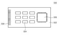
도 17은 본 발명의 실시예들에 따른 패키지 모듈(500)을 보여주는 평면도이다. 도 17을 참조하여, 상기 패키지 모듈(500)은 외부 연결 단자(508)가 구비된 모듈 기판(502)과, 상기 모듈 기판(502)에 실장된 반도체 칩(504) 및 QFP(Quad Flat Package)된 반도체 패키지(506)를 포함할 수 있다. 상기 반도체 칩(504) 및/또는 상기 반도체 패키지(506)는 본 발명의 실시예에 따른 반도체 장치를 포함할 수 있다. 상기 패키지 모듈(500)은 상기 외부 연결 단자(508)를 통해 외부 전자 장치와 연결될 수 있다.17 is a plan view showing a
도 18은 본 발명의 실시예들에 따른 메모리 카드(600)를 보여주는 개략도이다. 도 18을 참조하여, 상기 메모리 카드(600)는 하우징(610) 내에 제어기(620)와 메모리(630)를 포함할 수 있다. 상기 제어기(620)와 상기 메모리(630)는 전기적인 신호를 교환할 수 있다. 예를 들어, 상기 제어기(620)의 명령에 따라서, 상기 메모리(630)와 상기 제어기(620)는 데이터를 주고받을 수 있다. 이에 따라, 상기 메모리 카드(600)는 상기 메모리(630)에 데이터를 저장하거나 또는 상기 메모리(630)로부터 데이터를 외부로 출력할 수 있다.18 is a schematic diagram showing a
상기 제어기(620) 및/또는 상기 메모리(630)는 본 발명의 실시예들에 따른 반도체 장치 또는 반도체 패키지 중 적어도 하나를 포함할 수 있다. 이러한 상기 메모리 카드(600)는 다양한 휴대용 기기의 데이터 저장 매체로 이용될 수 있다. 예를 들어, 상기 메모리 카드(600)는 멀티미디어 카드(multi media card; MMC) 또는 보안 디지털(secure digital; SD) 카드를 포함할 수 있다.The
도 19는 본 발명의 실시예들에 따른 전자 시스템(700)을 보여주는 블록도이다. 도 19를 참조하여, 상기 전자 시스템(700)은 본 발명의 실시예들에 따른 반도체 장치 또는 반도체 패키지를 적어도 하나 포함할 수 있다. 상기 전자 시스템(700)은 모바일 기기나 컴퓨터 등을 포함할 수 있다. 예를 들어, 상기 전자 시스템(700)은 메모리 시스템(712), 프로세서(714), 램(716), 및 유저 인터페이스(718)를 포함할 수 고, 이들은 버스(Bus, 720)를 이용하여 서로 데이터 통신을 할 수 있다. 상기 프로세서(714)는 프로그램을 실행하고 상기 전자 시스템(700)을 제어하는 역할을 할 수 있다. 상기 램(716)은 상기 프로세서(714)의 동작 메모리로서 사용될 수 있다. 예를 들어, 상기 프로세서(714) 및 상기 램(716)은 각각 본 발명의 실시예들에 따른 반도체 장치 또는 반도체 패키지를 포함할 수 있다. 또는 상기 프로세서(714)와 상기 램(716)이 하나의 패키지에 포함될 수 있다. 상기 유저 인터페이스(718)는 상기 전자 시스템(700)에 데이터를 입력 또는 출력하는데 이용될 수 있다. 상기 메모리 시스템(712)은 상기 프로세서(714)의 동작을 위한 코드, 상기 프로세서(714)에 의해 처리된 데이터 또는 외부에서 입력된 데이터를 저장할 수 있다. 상기 메모리 시스템(712)은 제어기 및 메모리를 포함할 수 있으며, 도 17의 메모리 카드(600)와 실질적으로 동일하게 구성될 수 있다.19 is a block diagram illustrating an
상기 전자 시스템(도 19의 700)은 다양한 전자기기들의 전자 제어 장치에 적용될 수 있다. 도 20은 상기 전자 시스템(도 19의 700)이 모바일 폰(800)에 적용되는 예를 도시한다. 그 밖에, 상기 전자 시스템(도 19의 700)은 휴대용 노트북, MP3 플레이어, 네비게이션(Navigation), 고상 디스크(Solid state disk; SSD), 자동차 또는 가전 제품(Household appliances)에 적용될 수 있다.The electronic system (700 of FIG. 19) can be applied to an electronic control device of various electronic devices. Fig. 20 shows an example in which the electronic system (700 of Fig. 19) is applied to the
발명의 특정 실시예들에 대한 이상의 설명은 예시 및 설명을 목적으로 제공되었다. 따라서 본 발명은 상기 실시예들에 한정되지 않으며, 본 발명의 기술적 사상 내에서 해당 분야에서 통상의 지식을 가진 자에 의하여 상기 실시예들을 조합하여 실시하는 등 여러 가지 많은 수정 및 변경이 가능함은 명백하다.
The foregoing description of specific embodiments of the invention has been presented for purposes of illustration and description. It will be apparent to those skilled in the art that various modifications and variations can be made in the present invention without departing from the spirit and scope of the invention as defined by the appended claims. Do.
Claims (20)
Translated fromKorean상기 기판을 관통하는 비아홀 내의 관통 전극; 및
상기 관통 전극과 인접하여 상기 제 1 면에 제공된 집적 회로를 포함하고,
상기 관통 전극은:
상기 비아홀의 일부를 채우는 금속층; 및
상기 비아홀의 나머지 부분을 채우는 합금층을 포함하고,
상기 합금층의 결정립 크기는 상기 금속층의 결정립 크기보다 작고,
상기 합금층은 상기 금속층에 포함된 금속 원소 및 상기 금속층에 포함된 금속 원소와 다른 금속원소를 포함하고 구리를 포함하지 않는 반도체 장치.A substrate comprising a first surface and a second surface opposite the first surface;
A penetrating electrode in a via hole passing through the substrate; And
And an integrated circuit provided on the first surface adjacent to the penetrating electrode,
Wherein the penetrating electrode comprises:
A metal layer filling a part of the via hole; And
And an alloy layer filling the remaining portion of the via hole,
The grain size of the alloy layer is smaller than the grain size of the metal layer,
Wherein the alloy layer includes a metal element contained in the metal layer and a metal element different from the metal element contained in the metal layer and does not include copper.
상기 관통 전극은 상기 제 1 면에 인접한 상면 및 상기 제 2 면에 인접한 하면을 포함하고,
상기 합금층은 상기 관통 전극의 상면에서 노출된 반도체 장치.The method according to claim 1,
Wherein the penetrating electrode comprises an upper surface adjacent the first surface and a lower surface adjacent the second surface,
And the alloy layer is exposed on an upper surface of the penetrating electrode.
상기 금속층은 상기 합금층과 상기 비아홀의 측벽 사이로 연장되는 연장부를 포함하는 반도체 장치.The method according to claim 1,
Wherein the metal layer includes an extension portion extending between the alloy layer and a side wall of the via hole.
상기 합금층 상면의 직경은 상기 연장부의 두께보다 큰 반도체 장치.The method of claim 3,
And the diameter of the upper surface of the alloy layer is larger than the thickness of the extended portion.
상기 관통 전극과 상기 집적 회로를 전기적으로 연결하는 상부 배선을 더 포함하고,
상기 금속층과 상기 합금층은 상기 상부 배선에 공통적으로 접하는 반도체 장치.The method of claim 3,
Further comprising an upper wiring electrically connecting the penetrating electrode and the integrated circuit,
Wherein the metal layer and the alloy layer are in contact with the upper wiring in common.
상기 관통 전극은 상기 비아홀의 측벽을 따라 제공되는 배리어층을 더 포함하고,
상기 합금층은 상기 배리어층과 접하는 반도체 장치.The method according to claim 1,
Wherein the penetrating electrode further comprises a barrier layer provided along a side wall of the via hole,
And the alloy layer is in contact with the barrier layer.
상기 합금층의 두께는 상기 관통 전극의 총 길이의 2% 내지 15%인 반도체 장치.The method according to claim 1,
And the thickness of the alloy layer is 2% to 15% of the total length of the penetrating electrode.
상기 금속층의 평균 결정립 크기는 상기 합금층의 평균 결정립 크기의 2배 이상인 반도체 장치.The method according to claim 1,
Wherein the average grain size of the metal layer is at least twice the average grain size of the alloy layer.
상기 금속층은 텅스텐(W)을 포함하고, 상기 합금층은 W-Mn합금(Mn은 5atm% 내지 8atm%), W-Au합금(Au는 10atm%이상), 또는 W-Ni합금(Ni는 2atm%이상) 중 적어도 하나를 포함하는 반도체 장치.The method according to claim 1,
Wherein the metal layer comprises tungsten (W) and the alloy layer is a W-Mn alloy (Mn is 5 atm% to 8 atm%), a W-Au alloy (Au is at least 10 atm%), % Or more).
상기 집적 회로를 덮는 제 1 층간 절연막을 더 포함하고,
상기 관통 전극은, 상기 제 1 면에 대향하는, 상기 제 1 층간 절연막의 상면으로 연장되는 반도체 장치.The method according to claim 1,
Further comprising a first interlayer insulating film covering the integrated circuit,
And the penetrating electrode extends to the upper surface of the first interlayer insulating film, which is opposed to the first surface.
상기 합금층의 하면은 상기 제 1 면보다 높은 반도체 장치.13. The method of claim 12,
And the lower surface of the alloy layer is higher than the first surface.
상기 집적 회로를 덮는 제 1 층간 절연막을 더 포함하고,
상기 제 1 층간 절연막은 상기 관통 전극의 상면을 덮는 반도체 장치.The method according to claim 1,
Further comprising a first interlayer insulating film covering the integrated circuit,
And the first interlayer insulating film covers an upper surface of the penetrating electrode.
상기 집적 회로를 덮는 제 1 층간 절연막;
상기 제 1 층간 절연막 상의 금속 배선; 및
상기 금속 배선 상의 제 2 층간 절연막을 더 포함하고,
상기 관통 전극은, 상기 제 1 층간 절연막에 대향하는, 상기 제 2 층간 절연막의 상면으로 연장하는 반도체 장치.The method according to claim 1,
A first interlayer insulating film covering the integrated circuit;
A metal wiring on the first interlayer insulating film; And
Further comprising a second interlayer insulating film on the metal wiring,
And the penetrating electrode extends to the upper surface of the second interlayer insulating film, which is opposed to the first interlayer insulating film.
상기 비아홀 내의 관통 전극을 포함하고,
상기 관통 전극은 상기 비아홀의 일부를 채우는 금속층, 및 상기 금속층 상에 제공되고 상기 금속층에 포함된 금속 원소와 다른 금속 원소를 포함하고 구리를 포함하지 않는 합금층을 포함하고,
상기 금속층은 상기 합금층과 상기 비아홀의 측벽 사이로 연장되는 연장부를 포함하고,
상기 합금층의 결정립 크기는 상기 금속층의 결정립 크기보다 작은 반도체 장치.A substrate including an active surface, an inactive surface opposite to the active surface, and a via hole penetrating the active surface and the inactive surface; And
And a through electrode in the via hole,
Wherein the through electrode includes a metal layer that fills a portion of the via hole and an alloy layer that is provided on the metal layer and includes a metal element different from the metal element contained in the metal layer and does not include copper,
Wherein the metal layer includes an extension portion extending between the alloy layer and a side wall of the via hole,
And the grain size of the alloy layer is smaller than the grain size of the metal layer.
상기 금속층은 상기 합금층 아래의 바디부를 더 포함하고,
상기 연장부의 결정립 크기는 상기 바디부의 결정립 크기보다 작은 반도체 장치.17. The method of claim 16,
Wherein the metal layer further comprises a body portion below the alloy layer,
And the grain size of the extended portion is smaller than the grain size of the body portion.
상기 관통 전극과 인접하여 상기 기판의 활성면 상에 제공된 집적 회로; 및
상기 관통 전극과 상기 집적 회로를 전기적으로 연결하는 상부 배선을 더 포함하고,
상기 금속층과 상기 합금층은 상기 상부 배선에 공통적으로 접하는 반도체 장치.17. The method of claim 16,
An integrated circuit provided on the active surface of the substrate adjacent the penetrating electrode; And
Further comprising an upper wiring electrically connecting the penetrating electrode and the integrated circuit,
Wherein the metal layer and the alloy layer are in contact with the upper wiring in common.
상기 집적 회로를 덮는 층간 절연막을 더 포함하고,
상기 관통 전극은 상기 층간 절연막을 관통하여 상기 상부 배선과 연결되고,
상기 합금층의 하면은 상기 활성면보다 높은 반도체 장치.19. The method of claim 18,
Further comprising an interlayer insulating film covering the integrated circuit,
The penetrating electrode is connected to the upper wiring through the interlayer insulating film,
And the lower surface of the alloy layer is higher than the active surface.
상기 합금층은 상기 금속층에 포함된 금속 원소를 더 포함하는 반도체 장치.17. The method of claim 16,
Wherein the alloy layer further comprises a metal element contained in the metal layer.
Priority Applications (4)
| Application Number | Priority Date | Filing Date | Title |
|---|---|---|---|
| KR1020120106707AKR101992352B1 (en) | 2012-09-25 | 2012-09-25 | Semicondctor devices |
| US14/028,523US9153522B2 (en) | 2012-09-25 | 2013-09-16 | Semiconductor devices and methods of fabricating the same |
| JP2013197964AJP5865881B2 (en) | 2012-09-25 | 2013-09-25 | Semiconductor device and manufacturing method thereof |
| US14/809,159US9679829B2 (en) | 2012-09-25 | 2015-07-24 | Semiconductor devices and methods of fabricating the same |
Applications Claiming Priority (1)
| Application Number | Priority Date | Filing Date | Title |
|---|---|---|---|
| KR1020120106707AKR101992352B1 (en) | 2012-09-25 | 2012-09-25 | Semicondctor devices |
Publications (2)
| Publication Number | Publication Date |
|---|---|
| KR20140039895A KR20140039895A (en) | 2014-04-02 |
| KR101992352B1true KR101992352B1 (en) | 2019-06-24 |
Family
ID=50338075
Family Applications (1)
| Application Number | Title | Priority Date | Filing Date |
|---|---|---|---|
| KR1020120106707AActiveKR101992352B1 (en) | 2012-09-25 | 2012-09-25 | Semicondctor devices |
Country Status (3)
| Country | Link |
|---|---|
| US (2) | US9153522B2 (en) |
| JP (1) | JP5865881B2 (en) |
| KR (1) | KR101992352B1 (en) |
Families Citing this family (21)
| Publication number | Priority date | Publication date | Assignee | Title |
|---|---|---|---|---|
| US9673132B2 (en)* | 2012-04-27 | 2017-06-06 | Taiwan Semiconductor Manufacting Company, Ltd. | Interconnection structure with confinement layer |
| KR20140011137A (en)* | 2012-07-17 | 2014-01-28 | 삼성전자주식회사 | Integrated circuit device having through silicon via structure and method of manufacturing the same |
| CA2882646A1 (en)* | 2012-09-05 | 2014-03-13 | Research Triangle Institute | Electronic devices utilizing contact pads with protrusions and methods for fabrication |
| US9514986B2 (en)* | 2013-08-28 | 2016-12-06 | Taiwan Semiconductor Manufacturing Company, Ltd. | Device with capped through-substrate via structure |
| US9865523B2 (en) | 2014-01-17 | 2018-01-09 | Taiwan Semiconductor Manufacturing Company, Ltd. | Robust through-silicon-via structure |
| US9583417B2 (en)* | 2014-03-12 | 2017-02-28 | Invensas Corporation | Via structure for signal equalization |
| KR102320821B1 (en) | 2014-09-11 | 2021-11-02 | 삼성전자주식회사 | Semiconductor package |
| DE102014115105B4 (en) | 2014-10-09 | 2023-06-22 | Taiwan Semiconductor Manufacturing Company, Ltd. | Semiconductor device and method of manufacturing a semiconductor device |
| JP2016139648A (en) | 2015-01-26 | 2016-08-04 | 株式会社東芝 | Semiconductor device and manufacturing method of the same |
| US10074594B2 (en)* | 2015-04-17 | 2018-09-11 | Taiwan Semiconductor Manufacturing Company Ltd. | Semiconductor structure and manufacturing method thereof |
| US9761509B2 (en)* | 2015-12-29 | 2017-09-12 | United Microelectronics Corp. | Semiconductor device with throgh-substrate via and method for fabrication the semiconductor device |
| US10242932B2 (en) | 2016-06-24 | 2019-03-26 | Infineon Technologies Ag | LDMOS transistor and method |
| US9875933B2 (en) | 2016-06-24 | 2018-01-23 | Infineon Technologies Ag | Substrate and method including forming a via comprising a conductive liner layer and conductive plug having different microstructures |
| US10050139B2 (en) | 2016-06-24 | 2018-08-14 | Infineon Technologies Ag | Semiconductor device including a LDMOS transistor and method |
| US10622284B2 (en) | 2016-06-24 | 2020-04-14 | Infineon Technologies Ag | LDMOS transistor and method |
| US10432172B2 (en) | 2016-09-01 | 2019-10-01 | Samsung Electro-Mechanics Co., Ltd. | Bulk acoustic filter device and method of manufacturing the same |
| US10276528B2 (en)* | 2017-07-18 | 2019-04-30 | Taiwan Semiconductor Manufacturing Co., Ltd. | Semicondcutor device and manufacturing method thereof |
| KR102542614B1 (en)* | 2017-10-30 | 2023-06-15 | 삼성전자주식회사 | Image sensor |
| JP7219598B2 (en)* | 2018-11-27 | 2023-02-08 | 新光電気工業株式会社 | Wiring board and its manufacturing method |
| US11398408B2 (en)* | 2019-09-24 | 2022-07-26 | Advanced Semiconductor Engineering, Inc. | Semiconductor substrate with trace connected to via at a level within a dielectric layer |
| KR20230024298A (en)* | 2020-06-17 | 2023-02-20 | 도쿄엘렉트론가부시키가이샤 | Area-selective deposition method using surface cleaning process |
Citations (1)
| Publication number | Priority date | Publication date | Assignee | Title |
|---|---|---|---|---|
| US20110193199A1 (en)* | 2010-02-09 | 2011-08-11 | International Business Machines Corporation | Electromigration immune through-substrate vias |
Family Cites Families (35)
| Publication number | Priority date | Publication date | Assignee | Title |
|---|---|---|---|---|
| US5262354A (en)* | 1992-02-26 | 1993-11-16 | International Business Machines Corporation | Refractory metal capped low resistivity metal conductor lines and vias |
| US5300813A (en)* | 1992-02-26 | 1994-04-05 | International Business Machines Corporation | Refractory metal capped low resistivity metal conductor lines and vias |
| MY144573A (en)* | 1998-09-14 | 2011-10-14 | Ibiden Co Ltd | Printed circuit board and method for its production |
| US6884335B2 (en)* | 2003-05-20 | 2005-04-26 | Novellus Systems, Inc. | Electroplating using DC current interruption and variable rotation rate |
| US7019402B2 (en) | 2003-10-17 | 2006-03-28 | International Business Machines Corporation | Silicon chip carrier with through-vias using laser assisted chemical vapor deposition of conductor |
| US6979625B1 (en)* | 2003-11-12 | 2005-12-27 | Advanced Micro Devices, Inc. | Copper interconnects with metal capping layer and selective copper alloys |
| US8084866B2 (en) | 2003-12-10 | 2011-12-27 | Micron Technology, Inc. | Microelectronic devices and methods for filling vias in microelectronic devices |
| JP4800585B2 (en) | 2004-03-30 | 2011-10-26 | ルネサスエレクトロニクス株式会社 | Manufacturing method of through electrode, manufacturing method of silicon spacer |
| US7232513B1 (en)* | 2004-06-29 | 2007-06-19 | Novellus Systems, Inc. | Electroplating bath containing wetting agent for defect reduction |
| WO2006016678A1 (en)* | 2004-08-12 | 2006-02-16 | Nec Corporation | Semiconductor device and its manufacturing method |
| US7989958B2 (en)* | 2005-06-14 | 2011-08-02 | Cufer Assett Ltd. L.L.C. | Patterned contact |
| JP2007005404A (en) | 2005-06-21 | 2007-01-11 | Matsushita Electric Works Ltd | Method of forming through interconnection line in semiconductor substrate |
| JP4552770B2 (en) | 2005-06-21 | 2010-09-29 | パナソニック電工株式会社 | Method for forming through wiring on semiconductor substrate |
| JP4581864B2 (en) | 2005-06-21 | 2010-11-17 | パナソニック電工株式会社 | Method for forming through wiring on semiconductor substrate |
| US7528006B2 (en) | 2005-06-30 | 2009-05-05 | Intel Corporation | Integrated circuit die containing particle-filled through-silicon metal vias with reduced thermal expansion |
| US7772116B2 (en)* | 2005-09-01 | 2010-08-10 | Micron Technology, Inc. | Methods of forming blind wafer interconnects |
| US7892972B2 (en)* | 2006-02-03 | 2011-02-22 | Micron Technology, Inc. | Methods for fabricating and filling conductive vias and conductive vias so formed |
| JP5231733B2 (en) | 2006-11-27 | 2013-07-10 | パナソニック株式会社 | Through-hole wiring structure and method for forming the same |
| US7939941B2 (en) | 2007-06-27 | 2011-05-10 | Taiwan Semiconductor Manufacturing Company, Ltd. | Formation of through via before contact processing |
| US7973416B2 (en)* | 2008-05-12 | 2011-07-05 | Texas Instruments Incorporated | Thru silicon enabled die stacking scheme |
| US7678696B2 (en) | 2008-08-08 | 2010-03-16 | International Business Machines Corporation | Method of making through wafer vias |
| KR20100021856A (en) | 2008-08-18 | 2010-02-26 | 삼성전자주식회사 | Method of forming semiconductor device having tsv and related device |
| US8097953B2 (en) | 2008-10-28 | 2012-01-17 | Taiwan Semiconductor Manufacturing Company, Ltd. | Three-dimensional integrated circuit stacking-joint interface structure |
| US20100200408A1 (en)* | 2009-02-11 | 2010-08-12 | United Solar Ovonic Llc | Method and apparatus for the solution deposition of high quality oxide material |
| US8610283B2 (en)* | 2009-10-05 | 2013-12-17 | International Business Machines Corporation | Semiconductor device having a copper plug |
| KR101302564B1 (en) | 2009-10-28 | 2013-09-02 | 한국전자통신연구원 | Method of forming a via and method of fabricating chip stack package thereof |
| KR20110050957A (en)* | 2009-11-09 | 2011-05-17 | 삼성전자주식회사 | Through-via contact of semiconductor device and forming method |
| JP2011216867A (en)* | 2010-03-17 | 2011-10-27 | Tokyo Electron Ltd | Thin-film formation method |
| KR101692434B1 (en) | 2010-06-28 | 2017-01-18 | 삼성전자주식회사 | Semiconductor device and method of manufacturing the same |
| JP5504147B2 (en)* | 2010-12-21 | 2014-05-28 | 株式会社荏原製作所 | Electroplating method |
| JP2012151435A (en) | 2010-12-27 | 2012-08-09 | Elpida Memory Inc | Method for manufacturing semiconductor device |
| WO2013039603A1 (en)* | 2011-09-13 | 2013-03-21 | Adesto Technologies Corporation | Resistive switching devices having alloyed electrodes and methods of formation thereof |
| US8785790B2 (en)* | 2011-11-10 | 2014-07-22 | Invensas Corporation | High strength through-substrate vias |
| US9269612B2 (en)* | 2011-11-22 | 2016-02-23 | Taiwan Semiconductor Manufacturing Company, Ltd. | Mechanisms of forming damascene interconnect structures |
| KR20140011137A (en)* | 2012-07-17 | 2014-01-28 | 삼성전자주식회사 | Integrated circuit device having through silicon via structure and method of manufacturing the same |
- 2012
- 2012-09-25KRKR1020120106707Apatent/KR101992352B1/enactiveActive
- 2013
- 2013-09-16USUS14/028,523patent/US9153522B2/enactiveActive
- 2013-09-25JPJP2013197964Apatent/JP5865881B2/enactiveActive
- 2015
- 2015-07-24USUS14/809,159patent/US9679829B2/enactiveActive
Patent Citations (1)
| Publication number | Priority date | Publication date | Assignee | Title |
|---|---|---|---|---|
| US20110193199A1 (en)* | 2010-02-09 | 2011-08-11 | International Business Machines Corporation | Electromigration immune through-substrate vias |
Also Published As
| Publication number | Publication date |
|---|---|
| JP2014068014A (en) | 2014-04-17 |
| US9679829B2 (en) | 2017-06-13 |
| JP5865881B2 (en) | 2016-02-17 |
| KR20140039895A (en) | 2014-04-02 |
| US9153522B2 (en) | 2015-10-06 |
| US20150332967A1 (en) | 2015-11-19 |
| US20140084473A1 (en) | 2014-03-27 |
Similar Documents
| Publication | Publication Date | Title |
|---|---|---|
| KR101992352B1 (en) | Semicondctor devices | |
| KR102064863B1 (en) | Method of fabricating Semiconductor Devices Having TSV | |
| CN111613612B (en) | Semiconductor package including embedded surface mount device and method of forming the same | |
| US9698080B2 (en) | Conductor structure for three-dimensional semiconductor device | |
| US8786058B2 (en) | Semiconductor devices and methods of manufacturing the same | |
| KR101959284B1 (en) | Semiconductor device and method of forming the same | |
| US8836142B2 (en) | Semiconductor devices | |
| US12278222B2 (en) | Method of fabricating semiconductor package including sub-interposer substrates | |
| KR20140073163A (en) | Semiconductor device and method of forming the same | |
| US20150130078A1 (en) | Semiconductor chip and semiconductor package having same | |
| US20150123278A1 (en) | Semiconductor devices, methods of manufacturing the same, memory cards including the same and electronic systems including the same | |
| KR101801137B1 (en) | Semiconductor Devices and Methods of Fabricating the Same | |
| KR20090013417A (en) | Semiconductor package, wafer stack package using same, and manufacturing method thereof | |
| KR20140104778A (en) | Methods for fabricating semiconductor devices having through vias | |
| CN103378057B (en) | Semiconductor chip and method of forming same | |
| KR20140065282A (en) | Semiconductor device comprising tsv(through silicon via), and semiconductor package comprising the same | |
| US9059067B2 (en) | Semiconductor device with interposer and method manufacturing same | |
| US20140141569A1 (en) | Semiconductor devices having through-via and methods of fabricating the same | |
| US9431332B2 (en) | Semiconductor package | |
| US20250167123A1 (en) | Semiconductor die having a metal plate layer | |
| CN107452686A (en) | Semiconductor package including through-mold ball on raised pad and method of manufacturing same | |
| US20120049349A1 (en) | Semiconductor chips and methods of forming the same | |
| KR20150019089A (en) | Semiconductor devices having through vias and methods for fabricating the same | |
| KR20150016798A (en) | Semicondctor devices and methods for fabricating the same | |
| CN103378032A (en) | Semiconductor chip and method of forming same |
Legal Events
| Date | Code | Title | Description |
|---|---|---|---|
| PA0109 | Patent application | Patent event code:PA01091R01D Comment text:Patent Application Patent event date:20120925 | |
| PG1501 | Laying open of application | ||
| A201 | Request for examination | ||
| PA0201 | Request for examination | Patent event code:PA02012R01D Patent event date:20170918 Comment text:Request for Examination of Application Patent event code:PA02011R01I Patent event date:20120925 Comment text:Patent Application | |
| E902 | Notification of reason for refusal | ||
| PE0902 | Notice of grounds for rejection | Comment text:Notification of reason for refusal Patent event date:20181113 Patent event code:PE09021S01D | |
| E701 | Decision to grant or registration of patent right | ||
| PE0701 | Decision of registration | Patent event code:PE07011S01D Comment text:Decision to Grant Registration Patent event date:20190327 | |
| GRNT | Written decision to grant | ||
| PR0701 | Registration of establishment | Comment text:Registration of Establishment Patent event date:20190618 Patent event code:PR07011E01D | |
| PR1002 | Payment of registration fee | Payment date:20190619 End annual number:3 Start annual number:1 | |
| PG1601 | Publication of registration | ||
| PR1001 | Payment of annual fee | Payment date:20220525 Start annual number:4 End annual number:4 | |
| PR1001 | Payment of annual fee | Payment date:20240527 Start annual number:6 End annual number:6 | |
| PR1001 | Payment of annual fee | Payment date:20250522 Start annual number:7 End annual number:7 |