KR101987562B1 - Switching element and method of manufacturing switching element - Google Patents
Switching element and method of manufacturing switching elementDownload PDFInfo
- Publication number
- KR101987562B1 KR101987562B1KR1020170177063AKR20170177063AKR101987562B1KR 101987562 B1KR101987562 B1KR 101987562B1KR 1020170177063 AKR1020170177063 AKR 1020170177063AKR 20170177063 AKR20170177063 AKR 20170177063AKR 101987562 B1KR101987562 B1KR 101987562B1
- Authority
- KR
- South Korea
- Prior art keywords
- layer
- type semiconductor
- semiconductor layer
- semiconductor substrate
- insulating film
- Prior art date
- Legal status (The legal status is an assumption and is not a legal conclusion. Google has not performed a legal analysis and makes no representation as to the accuracy of the status listed.)
- Active
Links
- 238000004519manufacturing processMethods0.000titleclaimsdescription12
- 239000004065semiconductorSubstances0.000claimsabstractdescription145
- 239000000758substrateSubstances0.000claimsabstractdescription67
- 239000010410layerSubstances0.000claimsdescription227
- 239000002344surface layerSubstances0.000claimsdescription16
- 239000011229interlayerSubstances0.000claimsdescription15
- 239000012535impuritySubstances0.000claimsdescription10
- 238000005530etchingMethods0.000claimsdescription6
- 150000002500ionsChemical class0.000claimsdescription3
- 229910002601GaNInorganic materials0.000description28
- JMASRVWKEDWRBT-UHFFFAOYSA-NGallium nitrideChemical compound[Ga]#NJMASRVWKEDWRBT-UHFFFAOYSA-N0.000description28
- 230000005684electric fieldEffects0.000description16
- 238000010586diagramMethods0.000description9
- 230000000052comparative effectEffects0.000description8
- 238000009826distributionMethods0.000description8
- 238000000034methodMethods0.000description7
- 238000009792diffusion processMethods0.000description6
- 230000000694effectsEffects0.000description3
- VYPSYNLAJGMNEJ-UHFFFAOYSA-NSilicium dioxideChemical compoundO=[Si]=OVYPSYNLAJGMNEJ-UHFFFAOYSA-N0.000description2
- 239000012212insulatorSubstances0.000description2
- 229910052814silicon oxideInorganic materials0.000description2
- 239000013078crystalSubstances0.000description1
- 230000007547defectEffects0.000description1
- 230000000116mitigating effectEffects0.000description1
- 238000012986modificationMethods0.000description1
- 230000004048modificationEffects0.000description1
- 238000005498polishingMethods0.000description1
- 230000002250progressing effectEffects0.000description1
- 239000000126substanceSubstances0.000description1
Images


Classifications
- H—ELECTRICITY
- H10—SEMICONDUCTOR DEVICES; ELECTRIC SOLID-STATE DEVICES NOT OTHERWISE PROVIDED FOR
- H10D—INORGANIC ELECTRIC SEMICONDUCTOR DEVICES
- H10D64/00—Electrodes of devices having potential barriers
- H10D64/20—Electrodes characterised by their shapes, relative sizes or dispositions
- H10D64/23—Electrodes carrying the current to be rectified, amplified, oscillated or switched, e.g. sources, drains, anodes or cathodes
- H10D64/251—Source or drain electrodes for field-effect devices
- H—ELECTRICITY
- H10—SEMICONDUCTOR DEVICES; ELECTRIC SOLID-STATE DEVICES NOT OTHERWISE PROVIDED FOR
- H10D—INORGANIC ELECTRIC SEMICONDUCTOR DEVICES
- H10D30/00—Field-effect transistors [FET]
- H10D30/60—Insulated-gate field-effect transistors [IGFET]
- H10D30/64—Double-diffused metal-oxide semiconductor [DMOS] FETs
- H10D30/66—Vertical DMOS [VDMOS] FETs
- H—ELECTRICITY
- H10—SEMICONDUCTOR DEVICES; ELECTRIC SOLID-STATE DEVICES NOT OTHERWISE PROVIDED FOR
- H10D—INORGANIC ELECTRIC SEMICONDUCTOR DEVICES
- H10D30/00—Field-effect transistors [FET]
- H10D30/60—Insulated-gate field-effect transistors [IGFET]
- H—ELECTRICITY
- H10—SEMICONDUCTOR DEVICES; ELECTRIC SOLID-STATE DEVICES NOT OTHERWISE PROVIDED FOR
- H10D—INORGANIC ELECTRIC SEMICONDUCTOR DEVICES
- H10D99/00—Subject matter not provided for in other groups of this subclass
- H01L29/41725—
- H—ELECTRICITY
- H01—ELECTRIC ELEMENTS
- H01L—SEMICONDUCTOR DEVICES NOT COVERED BY CLASS H10
- H01L21/00—Processes or apparatus adapted for the manufacture or treatment of semiconductor or solid state devices or of parts thereof
- H01L21/02—Manufacture or treatment of semiconductor devices or of parts thereof
- H01L21/02104—Forming layers
- H01L21/02365—Forming inorganic semiconducting materials on a substrate
- H01L21/02518—Deposited layers
- H01L21/02521—Materials
- H01L21/02538—Group 13/15 materials
- H01L21/0254—Nitrides
- H—ELECTRICITY
- H01—ELECTRIC ELEMENTS
- H01L—SEMICONDUCTOR DEVICES NOT COVERED BY CLASS H10
- H01L21/00—Processes or apparatus adapted for the manufacture or treatment of semiconductor or solid state devices or of parts thereof
- H01L21/02—Manufacture or treatment of semiconductor devices or of parts thereof
- H01L21/04—Manufacture or treatment of semiconductor devices or of parts thereof the devices having potential barriers, e.g. a PN junction, depletion layer or carrier concentration layer
- H01L21/18—Manufacture or treatment of semiconductor devices or of parts thereof the devices having potential barriers, e.g. a PN junction, depletion layer or carrier concentration layer the devices having semiconductor bodies comprising elements of Group IV of the Periodic Table or AIIIBV compounds with or without impurities, e.g. doping materials
- H01L21/26—Bombardment with radiation
- H01L21/263—Bombardment with radiation with high-energy radiation
- H01L21/265—Bombardment with radiation with high-energy radiation producing ion implantation
- H01L21/2654—Bombardment with radiation with high-energy radiation producing ion implantation in AIIIBV compounds
- H01L21/26546—Bombardment with radiation with high-energy radiation producing ion implantation in AIIIBV compounds of electrically active species
- H—ELECTRICITY
- H01—ELECTRIC ELEMENTS
- H01L—SEMICONDUCTOR DEVICES NOT COVERED BY CLASS H10
- H01L21/00—Processes or apparatus adapted for the manufacture or treatment of semiconductor or solid state devices or of parts thereof
- H01L21/02—Manufacture or treatment of semiconductor devices or of parts thereof
- H01L21/04—Manufacture or treatment of semiconductor devices or of parts thereof the devices having potential barriers, e.g. a PN junction, depletion layer or carrier concentration layer
- H01L21/18—Manufacture or treatment of semiconductor devices or of parts thereof the devices having potential barriers, e.g. a PN junction, depletion layer or carrier concentration layer the devices having semiconductor bodies comprising elements of Group IV of the Periodic Table or AIIIBV compounds with or without impurities, e.g. doping materials
- H01L21/30—Treatment of semiconductor bodies using processes or apparatus not provided for in groups H01L21/20 - H01L21/26
- H01L21/302—Treatment of semiconductor bodies using processes or apparatus not provided for in groups H01L21/20 - H01L21/26 to change their surface-physical characteristics or shape, e.g. etching, polishing, cutting
- H01L21/306—Chemical or electrical treatment, e.g. electrolytic etching
- H01L21/30604—Chemical etching
- H01L21/30612—Etching of AIIIBV compounds
- H—ELECTRICITY
- H01—ELECTRIC ELEMENTS
- H01L—SEMICONDUCTOR DEVICES NOT COVERED BY CLASS H10
- H01L21/00—Processes or apparatus adapted for the manufacture or treatment of semiconductor or solid state devices or of parts thereof
- H01L21/02—Manufacture or treatment of semiconductor devices or of parts thereof
- H01L21/04—Manufacture or treatment of semiconductor devices or of parts thereof the devices having potential barriers, e.g. a PN junction, depletion layer or carrier concentration layer
- H01L21/18—Manufacture or treatment of semiconductor devices or of parts thereof the devices having potential barriers, e.g. a PN junction, depletion layer or carrier concentration layer the devices having semiconductor bodies comprising elements of Group IV of the Periodic Table or AIIIBV compounds with or without impurities, e.g. doping materials
- H01L21/30—Treatment of semiconductor bodies using processes or apparatus not provided for in groups H01L21/20 - H01L21/26
- H01L21/302—Treatment of semiconductor bodies using processes or apparatus not provided for in groups H01L21/20 - H01L21/26 to change their surface-physical characteristics or shape, e.g. etching, polishing, cutting
- H01L21/306—Chemical or electrical treatment, e.g. electrolytic etching
- H01L21/30625—With simultaneous mechanical treatment, e.g. mechanico-chemical polishing
- H—ELECTRICITY
- H01—ELECTRIC ELEMENTS
- H01L—SEMICONDUCTOR DEVICES NOT COVERED BY CLASS H10
- H01L21/00—Processes or apparatus adapted for the manufacture or treatment of semiconductor or solid state devices or of parts thereof
- H01L21/02—Manufacture or treatment of semiconductor devices or of parts thereof
- H01L21/04—Manufacture or treatment of semiconductor devices or of parts thereof the devices having potential barriers, e.g. a PN junction, depletion layer or carrier concentration layer
- H01L21/18—Manufacture or treatment of semiconductor devices or of parts thereof the devices having potential barriers, e.g. a PN junction, depletion layer or carrier concentration layer the devices having semiconductor bodies comprising elements of Group IV of the Periodic Table or AIIIBV compounds with or without impurities, e.g. doping materials
- H01L21/30—Treatment of semiconductor bodies using processes or apparatus not provided for in groups H01L21/20 - H01L21/26
- H01L21/302—Treatment of semiconductor bodies using processes or apparatus not provided for in groups H01L21/20 - H01L21/26 to change their surface-physical characteristics or shape, e.g. etching, polishing, cutting
- H01L21/306—Chemical or electrical treatment, e.g. electrolytic etching
- H01L21/308—Chemical or electrical treatment, e.g. electrolytic etching using masks
- H—ELECTRICITY
- H01—ELECTRIC ELEMENTS
- H01L—SEMICONDUCTOR DEVICES NOT COVERED BY CLASS H10
- H01L21/00—Processes or apparatus adapted for the manufacture or treatment of semiconductor or solid state devices or of parts thereof
- H01L21/70—Manufacture or treatment of devices consisting of a plurality of solid state components formed in or on a common substrate or of parts thereof; Manufacture of integrated circuit devices or of parts thereof
- H01L21/71—Manufacture of specific parts of devices defined in group H01L21/70
- H01L21/768—Applying interconnections to be used for carrying current between separate components within a device comprising conductors and dielectrics
- H01L21/76801—Applying interconnections to be used for carrying current between separate components within a device comprising conductors and dielectrics characterised by the formation and the after-treatment of the dielectrics, e.g. smoothing
- H01L21/76802—Applying interconnections to be used for carrying current between separate components within a device comprising conductors and dielectrics characterised by the formation and the after-treatment of the dielectrics, e.g. smoothing by forming openings in dielectrics
- H01L21/76805—Applying interconnections to be used for carrying current between separate components within a device comprising conductors and dielectrics characterised by the formation and the after-treatment of the dielectrics, e.g. smoothing by forming openings in dielectrics the opening being a via or contact hole penetrating the underlying conductor
- H—ELECTRICITY
- H01—ELECTRIC ELEMENTS
- H01L—SEMICONDUCTOR DEVICES NOT COVERED BY CLASS H10
- H01L21/00—Processes or apparatus adapted for the manufacture or treatment of semiconductor or solid state devices or of parts thereof
- H01L21/70—Manufacture or treatment of devices consisting of a plurality of solid state components formed in or on a common substrate or of parts thereof; Manufacture of integrated circuit devices or of parts thereof
- H01L21/71—Manufacture of specific parts of devices defined in group H01L21/70
- H01L21/768—Applying interconnections to be used for carrying current between separate components within a device comprising conductors and dielectrics
- H01L21/76838—Applying interconnections to be used for carrying current between separate components within a device comprising conductors and dielectrics characterised by the formation and the after-treatment of the conductors
- H01L21/76895—Local interconnects; Local pads, as exemplified by patent document EP0896365
- H—ELECTRICITY
- H01—ELECTRIC ELEMENTS
- H01L—SEMICONDUCTOR DEVICES NOT COVERED BY CLASS H10
- H01L21/00—Processes or apparatus adapted for the manufacture or treatment of semiconductor or solid state devices or of parts thereof
- H01L21/70—Manufacture or treatment of devices consisting of a plurality of solid state components formed in or on a common substrate or of parts thereof; Manufacture of integrated circuit devices or of parts thereof
- H01L21/71—Manufacture of specific parts of devices defined in group H01L21/70
- H01L21/768—Applying interconnections to be used for carrying current between separate components within a device comprising conductors and dielectrics
- H01L21/76897—Formation of self-aligned vias or contact plugs, i.e. involving a lithographically uncritical step
- H—ELECTRICITY
- H01—ELECTRIC ELEMENTS
- H01L—SEMICONDUCTOR DEVICES NOT COVERED BY CLASS H10
- H01L23/00—Details of semiconductor or other solid state devices
- H01L23/52—Arrangements for conducting electric current within the device in operation from one component to another, i.e. interconnections, e.g. wires, lead frames
- H01L23/535—Arrangements for conducting electric current within the device in operation from one component to another, i.e. interconnections, e.g. wires, lead frames including internal interconnections, e.g. cross-under constructions
- H01L29/66227—
- H—ELECTRICITY
- H10—SEMICONDUCTOR DEVICES; ELECTRIC SOLID-STATE DEVICES NOT OTHERWISE PROVIDED FOR
- H10D—INORGANIC ELECTRIC SEMICONDUCTOR DEVICES
- H10D12/00—Bipolar devices controlled by the field effect, e.g. insulated-gate bipolar transistors [IGBT]
- H10D12/01—Manufacture or treatment
- H—ELECTRICITY
- H10—SEMICONDUCTOR DEVICES; ELECTRIC SOLID-STATE DEVICES NOT OTHERWISE PROVIDED FOR
- H10D—INORGANIC ELECTRIC SEMICONDUCTOR DEVICES
- H10D12/00—Bipolar devices controlled by the field effect, e.g. insulated-gate bipolar transistors [IGBT]
- H10D12/01—Manufacture or treatment
- H10D12/031—Manufacture or treatment of IGBTs
- H—ELECTRICITY
- H10—SEMICONDUCTOR DEVICES; ELECTRIC SOLID-STATE DEVICES NOT OTHERWISE PROVIDED FOR
- H10D—INORGANIC ELECTRIC SEMICONDUCTOR DEVICES
- H10D30/00—Field-effect transistors [FET]
- H10D30/01—Manufacture or treatment
- H10D30/021—Manufacture or treatment of FETs having insulated gates [IGFET]
- H10D30/028—Manufacture or treatment of FETs having insulated gates [IGFET] of double-diffused metal oxide semiconductor [DMOS] FETs
- H10D30/0291—Manufacture or treatment of FETs having insulated gates [IGFET] of double-diffused metal oxide semiconductor [DMOS] FETs of vertical DMOS [VDMOS] FETs
- H—ELECTRICITY
- H10—SEMICONDUCTOR DEVICES; ELECTRIC SOLID-STATE DEVICES NOT OTHERWISE PROVIDED FOR
- H10D—INORGANIC ELECTRIC SEMICONDUCTOR DEVICES
- H10D48/00—Individual devices not covered by groups H10D1/00 - H10D44/00
- H10D48/01—Manufacture or treatment
- H10D48/031—Manufacture or treatment of three-or-more electrode devices
- H—ELECTRICITY
- H10—SEMICONDUCTOR DEVICES; ELECTRIC SOLID-STATE DEVICES NOT OTHERWISE PROVIDED FOR
- H10D—INORGANIC ELECTRIC SEMICONDUCTOR DEVICES
- H10D62/00—Semiconductor bodies, or regions thereof, of devices having potential barriers
- H10D62/10—Shapes, relative sizes or dispositions of the regions of the semiconductor bodies; Shapes of the semiconductor bodies
- H10D62/102—Constructional design considerations for preventing surface leakage or controlling electric field concentration
- H10D62/103—Constructional design considerations for preventing surface leakage or controlling electric field concentration for increasing or controlling the breakdown voltage of reverse-biased devices
- H10D62/105—Constructional design considerations for preventing surface leakage or controlling electric field concentration for increasing or controlling the breakdown voltage of reverse-biased devices by having particular doping profiles, shapes or arrangements of PN junctions; by having supplementary regions, e.g. junction termination extension [JTE]
- H10D62/109—Reduced surface field [RESURF] PN junction structures
- H—ELECTRICITY
- H10—SEMICONDUCTOR DEVICES; ELECTRIC SOLID-STATE DEVICES NOT OTHERWISE PROVIDED FOR
- H10D—INORGANIC ELECTRIC SEMICONDUCTOR DEVICES
- H10D62/00—Semiconductor bodies, or regions thereof, of devices having potential barriers
- H10D62/10—Shapes, relative sizes or dispositions of the regions of the semiconductor bodies; Shapes of the semiconductor bodies
- H10D62/17—Semiconductor regions connected to electrodes not carrying current to be rectified, amplified or switched, e.g. channel regions
- H10D62/393—Body regions of DMOS transistors or IGBTs
- H—ELECTRICITY
- H10—SEMICONDUCTOR DEVICES; ELECTRIC SOLID-STATE DEVICES NOT OTHERWISE PROVIDED FOR
- H10D—INORGANIC ELECTRIC SEMICONDUCTOR DEVICES
- H10D62/00—Semiconductor bodies, or regions thereof, of devices having potential barriers
- H10D62/80—Semiconductor bodies, or regions thereof, of devices having potential barriers characterised by the materials
- H10D62/83—Semiconductor bodies, or regions thereof, of devices having potential barriers characterised by the materials being Group IV materials, e.g. B-doped Si or undoped Ge
- H10D62/832—Semiconductor bodies, or regions thereof, of devices having potential barriers characterised by the materials being Group IV materials, e.g. B-doped Si or undoped Ge being Group IV materials comprising two or more elements, e.g. SiGe
- H10D62/8325—Silicon carbide
- H—ELECTRICITY
- H10—SEMICONDUCTOR DEVICES; ELECTRIC SOLID-STATE DEVICES NOT OTHERWISE PROVIDED FOR
- H10D—INORGANIC ELECTRIC SEMICONDUCTOR DEVICES
- H10D62/00—Semiconductor bodies, or regions thereof, of devices having potential barriers
- H10D62/80—Semiconductor bodies, or regions thereof, of devices having potential barriers characterised by the materials
- H10D62/85—Semiconductor bodies, or regions thereof, of devices having potential barriers characterised by the materials being Group III-V materials, e.g. GaAs
- H10D62/8503—Nitride Group III-V materials, e.g. AlN or GaN
- H—ELECTRICITY
- H10—SEMICONDUCTOR DEVICES; ELECTRIC SOLID-STATE DEVICES NOT OTHERWISE PROVIDED FOR
- H10D—INORGANIC ELECTRIC SEMICONDUCTOR DEVICES
- H10D12/00—Bipolar devices controlled by the field effect, e.g. insulated-gate bipolar transistors [IGBT]
- H10D12/01—Manufacture or treatment
- H10D12/031—Manufacture or treatment of IGBTs
- H10D12/032—Manufacture or treatment of IGBTs of vertical IGBTs
- H—ELECTRICITY
- H10—SEMICONDUCTOR DEVICES; ELECTRIC SOLID-STATE DEVICES NOT OTHERWISE PROVIDED FOR
- H10D—INORGANIC ELECTRIC SEMICONDUCTOR DEVICES
- H10D12/00—Bipolar devices controlled by the field effect, e.g. insulated-gate bipolar transistors [IGBT]
- H10D12/411—Insulated-gate bipolar transistors [IGBT]
- H10D12/441—Vertical IGBTs
Landscapes
- Engineering & Computer Science (AREA)
- Physics & Mathematics (AREA)
- Computer Hardware Design (AREA)
- Microelectronics & Electronic Packaging (AREA)
- Power Engineering (AREA)
- Condensed Matter Physics & Semiconductors (AREA)
- General Physics & Mathematics (AREA)
- Manufacturing & Machinery (AREA)
- High Energy & Nuclear Physics (AREA)
- Chemical & Material Sciences (AREA)
- General Chemical & Material Sciences (AREA)
- Chemical Kinetics & Catalysis (AREA)
- Health & Medical Sciences (AREA)
- Toxicology (AREA)
- Electrodes Of Semiconductors (AREA)
- Insulated Gate Type Field-Effect Transistor (AREA)
- Recrystallisation Techniques (AREA)
- Thyristors (AREA)
Abstract
Translated fromKoreanDescription
Translated fromKorean본 개시는, 스위칭 소자 및 스위칭 소자의 제조 방법에 관한 것이다.This disclosure relates to a switching device and a manufacturing method of the switching device.
일본 특허 공개 제2009-147381호에, 제1 n형 반도체층(드리프트 영역)과, p형의 바디층과, 제2 n형 반도체층(소스 영역)을 갖는 스위칭 소자가 개시되어 있다. 제2 n형 반도체층은, 바디층에 의해 제1 n형 반도체층으로부터 분리되어 있다. 제1 n형 반도체층과 제2 n형 반도체층을 분리하고 있는 범위의 바디층에 대하여, 게이트 전극이 게이트 절연막을 개재시켜 대향하고 있다. 상기 스위칭 소자에서는, 제1 n형 반도체층과 바디층의 계면이, 바디층의 단부로부터 이격됨에 따라 바디층의 깊이가 깊어지도록 경사진 경사면을 갖는다. 경사면은, 게이트 전극의 하부에 배치되어 있다.Japanese Patent Laying-Open No. 2009-147381 discloses a switching device having a first n-type semiconductor layer (drift region), a p-type body layer, and a second n-type semiconductor layer (source region). The second n-type semiconductor layer is separated from the first n-type semiconductor layer by a body layer. The gate electrode is opposed to the body layer in the range separating the first n-type semiconductor layer and the second n-type semiconductor layer with the gate insulating film interposed therebetween. In the switching element, the interface between the first n-type semiconductor layer and the body layer has an inclined surface inclined so that the depth of the body layer becomes deeper as the body is separated from the end of the body layer. The inclined surface is disposed below the gate electrode.
본원 발명자들의 연구에 의해, 게이트 전극의 하부의 바디층과 제1 n형 반도체층의 계면에 경사면을 마련함으로써, 게이트 절연막에 인가되는 전계를 완화할 수 있음이 판명되었다.The inventors of the present invention have found that it is possible to alleviate the electric field applied to the gate insulating film by providing the inclined surface at the interface between the body layer under the gate electrode and the first n-type semiconductor layer.
일본 특허 공개 제2009-147381호의 스위칭 소자에서는, 게이트 전극의 하부의 바디층과 제1 n형 반도체층의 계면에 경사면이 마련되어 있다. 단, 일본 특허 공개 제2009-147381호에서는, 바디층이 확산층에 의해 구성되어 있다. 확산층에 의해 바디층이 구성되어 있는 경우, 바디층측으로부터 제1 n형 반도체층측을 향하여 불순물의 확산이 발생하므로, 경사면이 제1 n형 반도체층측으로 볼록해지도록 만곡된 형상으로 된다. 이와 같이 경사면이 만곡되면, 경사면이 상대적으로 좁아져, 게이트 절연막에 인가되는 전계를 완화하는 효과가 상대적으로 작아진다. 따라서, 본 명세서에서는 게이트 절연막에 인가되는 전계를 보다 효과적으로 완화할 수 있는 스위칭 소자를 제공한다.In the switching element of Japanese Patent Application Laid-Open No. 2009-147381, an inclined surface is provided at the interface between the body layer under the gate electrode and the first n-type semiconductor layer. However, in Japanese Patent Laying-Open No. 2009-147381, the body layer is composed of a diffusion layer. In the case where the body layer is constituted by the diffusion layer, diffusion of impurities occurs from the body layer side to the first n-type semiconductor layer side, so that the inclined surface is curved so as to be convex toward the first n-type semiconductor layer. When the inclined surface is curved in this manner, the inclined surface becomes relatively narrow, and the effect of alleviating the electric field applied to the gate insulating film becomes relatively small. Therefore, the present specification provides a switching device capable of more effectively mitigating the electric field applied to the gate insulating film.
본 개시의 제1 형태의 스위칭 소자는, 상기 반도체 기판의 표면에 노출되어 있는 제1 n형 반도체층과, 상기 반도체 기판의 상기 표면에 노출되어 있는 에피택셜층에 의해 구성되어 있는 p형의 바디층과, 상기 반도체 기판의 상기 표면에 노출되어 있고, 상기 바디층에 의해 상기 제1 n형 반도체층으로부터 분리되어 있는 제2 n형 반도체층을 갖는 반도체 기판, 상기 제1 n형 반도체층의 표면과, 상기 제1 n형 반도체층과 상기 제2 n형 반도체층의 사이의 상기 바디층의 표면과, 상기 제2 n형 반도체층의 표면에 걸치는 범위를 덮는 게이트 절연막, 및 상기 게이트 절연막을 개재시켜, 상기 제1 n형 반도체층과 상기 제2 n형 반도체층의 사이의 상기 바디층에 대향하는 게이트 전극을 구비한다. 상기 제1 n형 반도체층과 상기 바디층의 계면이 경사면을 갖는다. 상기 경사면은 상기 바디층의 단부로부터 횡방향으로 이격됨에 따라 상기 바디층의 깊이가 깊어지도록 경사진 경사면을 갖는다. 상기 경사면이, 상기 게이트 전극의 하부에 배치되어 있다.The switching element of the first aspect of the present disclosure includes a first n-type semiconductor layer exposed on a surface of the semiconductor substrate and a p-type body constituted by an epitaxial layer exposed on the surface of the semiconductor substrate A semiconductor substrate having a first n-type semiconductor layer and a second n-type semiconductor layer exposed on the surface of the semiconductor substrate and separated from the first n-type semiconductor layer by the body layer; A gate insulating film covering a surface of the body layer between the first n-type semiconductor layer and the second n-type semiconductor layer and a surface extending over the surface of the second n-type semiconductor layer; And a gate electrode facing the body layer between the first n-type semiconductor layer and the second n-type semiconductor layer. The interface between the first n-type semiconductor layer and the body layer has an inclined surface. The inclined surface has an inclined surface that is inclined to deepen the depth of the body layer as the inclined surface is laterally spaced from the end of the body layer. The inclined surface is disposed below the gate electrode.
본 개시의 제1 형태의 스위칭 소자에서는, 게이트 전극의 하부의 바디층과 제1 n형 반도체층의 계면에 경사면이 마련되어 있다. 또한, 상기 스위칭 소자에서는, 바디층이 에피택셜층에 의해 구성되어 있고, 바디층측으로부터 제1 n형 반도체층측으로의 불순물의 확산이 거의 발생하지 않는다. 따라서, 상기 스위칭 소자의 구조에 따르면, 바디층과 제1 n형 반도체층의 계면에 거의 만곡되어 있지 않은 경사면을 마련할 수 있고, 상대적으로 넓은 경사면을 얻을 수 있다. 따라서, 상기 구조에 따르면, 게이트 절연막에 인가되는 전계를 효과적으로 완화할 수 있다.In the switching element of the first aspect of the present disclosure, an inclined surface is provided at the interface between the body layer under the gate electrode and the first n-type semiconductor layer. In the switching element, the body layer is formed of an epitaxial layer, and diffusion of impurities from the body layer side to the first n-type semiconductor layer side hardly occurs. Therefore, according to the structure of the switching element, it is possible to provide an inclined surface which is not substantially curved at the interface between the body layer and the first n-type semiconductor layer, and a relatively wide inclined surface can be obtained. Therefore, according to the above structure, the electric field applied to the gate insulating film can be effectively mitigated.
본 개시의 제1 형태의 스위칭 소자에 있어서, 상기 경사면의 상기 반도체 기판의 상기 표면에 대한 각도가 60°미만이어도 된다.In the switching element of the first aspect of the present disclosure, the angle of the inclined surface with respect to the surface of the semiconductor substrate may be less than 60 degrees.
본 개시의 제1 형태의 스위칭 소자에 있어서, 상기 계면이, 상기 게이트 전극의 하부에 있어서 상기 반도체 기판의 상기 표면으로부터 하측 방향으로 신장되고, 상기 반도체 기판의 상기 표면에 대한 각도가 80°이상 90°이하인 표층부 계면을 갖고, 상기 경사면이, 상기 표층부 계면의 하측에 위치하고, 상기 경사면의 상기 반도체 기판의 상기 표면에 대한 각도가 60°미만이어도 된다.In the switching element according to the first aspect of the disclosure, the interface extends in a downward direction from the surface of the semiconductor substrate at a lower portion of the gate electrode, and the angle of the semiconductor substrate with respect to the surface is at least 80 degrees Or less and the inclined surface may be located below the surface layer interface and the angle of the inclined surface with respect to the surface of the semiconductor substrate may be less than 60 DEG.
본 개시의 제1 형태의 스위칭 소자에 있어서, 상기 반도체 기판은 상기 바디층과 상기 제2 n형 반도체층을 적어도 2개 포함하고, 상기 게이트 절연막은, 상기 제1 n형 반도체층 중 2개의 상기 바디층의 사이에 위치하는 부분인 간격부의 표면과, 상기 간격부와 상기 제2 n형 반도체층의 사이에 위치하는 부분인 상기 바디층의 표면과, 상기 제2 n형 반도체층의 표면의 일부에 걸치는 범위를 덮어도 된다.In the switching element according to the first aspect of the present disclosure, the semiconductor substrate includes at least two of the body layer and the second n-type semiconductor layer, and the gate insulating film includes two of the first n- And a surface of the body layer that is a portion located between the spacing portion and the second n-type semiconductor layer, and a portion of the surface of the second n-type semiconductor layer May be covered.
본 개시의 제2 형태의 스위칭 소자의 제조 방법은, 상기 반도체 기판의 표면에 노출되어 있는 제1 n형 반도체층과, p형의 바디층과, 상기 반도체 기판의 상기 표면에 노출되어 있고, 상기 바디층에 의해 상기 제1 n형 반도체층으로부터 분리되어 있는 제2 n형 반도체층을 갖는 반도체 기판과, 게이트 절연막과, 상기 게이트 절연막을 개재시켜, 상기 제1 n형 반도체층과 상기 제2 n형 반도체층의 사이의 상기 바디층에 대향하는 게이트 전극을 구비하는 스위칭 소자의 제조 방법이며, 상기 반도체 기판의 상면에 개구를 갖는 마스크를 형성하는 것과, 상기 개구의 상기 반도체 기판의 상면을 에칭하여 오목부를 형성하는 것과, 상기 에칭에서는 상기 오목부의 측면이 상기 반도체 기판의 상면에 대하여, 상기 오목부의 단부로부터 횡방향을 향하여 이격됨에 따라 상기 오목부의 깊이가 깊어지도록 경사진 경사면으로 되도록, 상기 오목부를 형성하는 것과, 상기 마스크를 제거하는 것과, 에피택셜 성장에 의해, 상기 반도체 기판의 상면과 상기 오목부 내에, 상기 바디층을 에피택셜 성장시키는 것과, 상기 반도체 기판의 상면을 연마하는 것과, 상기 바디층의 일부에 선택적으로 n형 불순물 이온을 주입하고, 상기 제2 n형 반도체층을 형성하는 것과, 상기 게이트 절연막을, 상기 제1 n형 반도체층의 표면과, 상기 제1 n형 반도체층과 상기 제2 n형 반도체층의 사이의 상기 바디층의 표면과, 상기 제2 n형 반도체층의 표면에 걸치는 범위를 덮도록 형성하는 것과, 상기 게이트 절연막의 상면 전체를 덮도록 상기 게이트 전극을 형성하는 것과, 상기 반도체 기판 표면 및 상기 게이트 전극의 표면을 덮도록 층간 절연막을 형성하는 것과, 상기 층간 절연막에 마련된 콘택트 홀 내에 콘택트 플러그를 형성하는 것과, 상기 층간 절연막의 상면에 상부 전극을 배치하는 것과, 상기 반도체 기판 중 상기 층간 절연막이 형성되는 면과는 반대의 면에 하부 전극을 배치하는 것을 구비한다.A manufacturing method of a switching element according to a second aspect of the present disclosure is a manufacturing method of a switching element including a first n-type semiconductor layer exposed on a surface of a semiconductor substrate, a p-type body layer, And a second n-type semiconductor layer separated from the first n-type semiconductor layer by a body layer, a gate insulating film, and a second n-type semiconductor layer interposed between the first n-type semiconductor layer and the second n- And a gate electrode facing the body layer between the first semiconductor layer and the second semiconductor layer, the method comprising: forming a mask having an opening in an upper surface of the semiconductor substrate; etching the upper surface of the semiconductor substrate in the opening And the side surface of the concave portion is spaced apart from the upper surface of the semiconductor substrate in the lateral direction from the end portion of the concave portion in the etching Forming the concave portion so that the concave portion is inclined so as to deepen the depth of the concave portion; removing the mask; and epitaxially growing the body layer in the concave portion of the semiconductor substrate, Implanting n-type impurity ions selectively into a part of the body layer to form the second n-type semiconductor layer; and forming the gate insulating film on the first type semiconductor layer so as to cover the surface of the n-type semiconductor layer, the surface of the body layer between the first n-type semiconductor layer and the second n-type semiconductor layer, and the surface of the second n- Forming the gate electrode so as to cover the entire upper surface of the gate insulating film, forming an interlayer insulating film so as to cover the surface of the semiconductor substrate and the surface of the gate electrode Forming a contact plug in a contact hole provided in the interlayer insulating film; disposing an upper electrode on an upper surface of the interlayer insulating film; forming a lower electrode on a surface of the semiconductor substrate opposite to the surface on which the interlayer insulating film is formed; As shown in FIG.
본 발명의 예시적인 실시 형태의 특징, 이점, 기술적 및 산업적 의의는 첨부된 도면을 참조하여 이하에서 설명될 것이며, 동일한 도면 부호는 동일한 요소를 나타낸다.
도 1은, 실시예 1의 MOSFET의 종단면도이다.
도 2는, 상대적으로 넓은 경사면을 갖는 MOSFET의 전계 분포를 도시하는 도면이다.
도 3은, 비교예 1의 MOSFET의 전계 분포를 도시하는 도면이다.
도 4는, 비교예 2의 MOSFET의 전계 분포를 도시하는 도면이다.
도 5는, 온 저항을 비교하는 그래프이다.
도 6은, 게이트 절연막에 인가되는 전계를 비교하는 그래프이다.
도 7은, 실시예 1의 MOSFET의 제조 공정의 설명도이다.
도 8은, 실시예 1의 MOSFET의 제조 공정의 설명도이다.
도 9는, 실시예 1의 MOSFET의 제조 공정의 설명도이다.
도 10은, 실시예 1의 MOSFET의 제조 공정의 설명도이다.
도 11은, 실시예 1의 MOSFET의 제조 공정의 설명도이다.
도 12는, 실시예 2의 MOSFET의 종단면도이다.
도 13은, 실시예 2의 MOSFET의 제조 공정의 설명도이다.The features, advantages, technical and industrial significance of exemplary embodiments of the present invention will be described below with reference to the accompanying drawings, in which like numerals represent like elements.
1 is a longitudinal sectional view of a MOSFET according to a first embodiment.
2 is a diagram showing an electric field distribution of a MOSFET having a relatively wide inclined plane.
3 is a diagram showing the electric field distribution of the MOSFET of Comparative Example 1. Fig.
4 is a diagram showing the electric field distribution of the MOSFET of Comparative Example 2. Fig.
5 is a graph comparing the on-resistance.
6 is a graph comparing an electric field applied to the gate insulating film.
7 is an explanatory diagram of a manufacturing process of a MOSFET according to the first embodiment.
8 is an explanatory diagram of a manufacturing process of the MOSFET of the first embodiment.
Fig. 9 is an explanatory diagram of a manufacturing process of the MOSFET of the first embodiment.
10 is an explanatory diagram of a manufacturing process of a MOSFET according to the first embodiment.
11 is an explanatory diagram of a manufacturing process of a MOSFET according to the first embodiment.
12 is a longitudinal sectional view of the MOSFET of the second embodiment.
13 is an explanatory diagram of a manufacturing process of the MOSFET of the second embodiment.
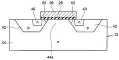
도 1에 도시하는 MOSFET(10)는, GaN 반도체 기판(12)을 갖고 있다. GaN 반도체 기판(12)은, GaN(질화갈륨)을 주성분으로 하는 반도체 기판이다.The
GaN 반도체 기판(12)은, 복수의 소스층(40), 복수의 바디층(42) 및 드리프트층(44)을 갖고 있다.The GaN
각 소스층(40)은 n형 영역이며, GaN 반도체 기판(12)의 상면(12a)에 노출되어 있다.Each
각 바디층(42)은 p형 영역이며, 대응하는 소스층(40)의 주위에 배치되어 있다. 각 바디층(42)은, 대응하는 소스층(40)의 측면과 하면을 덮고 있다. 각 바디층(42)은, 소스층(40)에 인접하는 범위에서, GaN 반도체 기판(12)의 상면(12a)에 노출되어 있다.Each
드리프트층(44)은 n형 영역이며, 각 바디층(42)의 하측에 배치되어 있다. 또한, 한 쌍의 바디층(42)의 사이에도 드리프트층(44)이 배치되어 있다. 이하에서는, 드리프트층(44) 중 한 쌍의 바디층(42)의 사이에 위치하는 부분을, 간격부(44a)라고 한다. 간격부(44a)는, JFET 영역이라고 불리는 경우가 있다. 간격부(44a)는, GaN 반도체 기판(12)의 상면(12a)에 노출되어 있다. 또한, 드리프트층(44)은, GaN 반도체 기판(12)의 하면(12b)의 대략 전역에 노출되어 있다. 드리프트층(44)은, 각 바디층(42)에 의해, 각 소스층(40)으로부터 분리되어 있다.The
바디층(42)과 드리프트층(44)의 사이의 계면(50)은, pn 접합면이다. 바디층(42)과 간격부(44a)의 사이의 부분의 계면(50)에, 경사면(52)이 마련되어 있다. 경사면(52)은, GaN 반도체 기판(12)의 상면(12a)으로부터 비스듬하게 하측 방향으로 신장되어 있다. 경사면(52)은, 바디층(42)의 저면까지 신장되어 있다. 경사면(52)은, 바디층(42)의 단부(42a)로부터 횡방향(상면(12a)과 평행한 방향)을 따라 이격됨에 따라 바디층(42)의 깊이(즉, 상면(12a)과 바디층(42)의 하단의 사이의 거리)가 깊어지도록 상면(12a)에 대하여 경사져 있다. 경사면(52)과 상면(12a)의 사이의 각도 θ(바디층(42) 내에서 측정되는 각도)는, 60°미만이다. 바디층(42)의 저부에서는, 계면(50)이 상면(12a)과 대략 평행으로 신장되어 있다.The
GaN 반도체 기판(12)의 상면(12a)에는, 게이트 절연막(28), 게이트 전극(26), 층간 절연막(24), 콘택트 플러그(22) 및 상부 전극(20)이 배치되어 있다.A
게이트 절연막(28)은, GaN 반도체 기판(12)의 상면(12a)의 일부를 덮고 있다. 게이트 절연막(28)은, 바디층(42) 근방의 소스층(40)의 표면과, 소스층(40)과 간격부(44a)의 사이의 바디층(42)의 표면과, 간격부(44a)의 표면에 걸치는 범위를 덮고 있다. 각 바디층(42) 중, 게이트 절연막(28)에 접하는 부분(즉, 소스층(40)과 간격부(44a)의 사이의 바디층(42)의 표층부)은, 채널이 형성되는 채널 영역(42b)이다. 게이트 절연막(28)은, 예를 들어 산화실리콘 등의 절연체에 의해 구성되어 있다.The
게이트 전극(26)은, 게이트 절연막(28) 상에 배치되어 있다. 게이트 전극(26)은, 게이트 절연막(28)을 개재시켜, 소스층(40), 바디층(42)(즉, 채널 영역(42b)) 및 드리프트층(44)(즉, 간격부(44a))에 대향하고 있다. 게이트 전극(26)은, 게이트 절연막(28)에 의해 GaN 반도체 기판(12)으로부터 절연되어 있다.The
층간 절연막(24)은, 게이트 절연막(28)에 덮여 있지 않은 범위의 상면(12a)을 덮고 있다. 또한, 층간 절연막(24)은, 게이트 전극(26)의 표면을 덮고 있다. 층간 절연막(24)은, 예를 들어 산화실리콘 등의 절연체에 의해 구성되어 있다.The
층간 절연막(24)에는 복수의 콘택트 홀이 형성되어 있고, 상기 복수의 콘택트 홀 내에 콘택트 플러그(22)가 설치되어 있다. 일부의 콘택트 플러그(22)는, 그 하단에서 소스층(40)에 접속되어 있고, 다른 콘택트 플러그(22)는, 그 하단에서 바디층(42)에 접속되어 있다.A plurality of contact holes are formed in the
상부 전극(20)은, 층간 절연막(24) 상에 배치되어 있다. 상부 전극(20)은, 각 콘택트 플러그(22)의 상면에 접해 있다. 상부 전극(20)은, 콘택트 플러그(22)를 통하여, 소스층(40) 및 바디층(42)에 접속되어 있다.The
GaN 반도체 기판(12)의 하면(12b)에는, 하부 전극(30)이 배치되어 있다. 하부 전극(30)은, 드리프트층(44)에 접속되어 있다.On the
게이트 전극(26)의 전위를 게이트 역치(MOSFET(10)를 온시키는 데 필요한 최소의 게이트 전위) 이상까지 높게 하면, 바디층(42)의 채널 영역(42b)에 전자가 끌어 당겨짐으로써, 채널 영역(42b)에 채널이 형성된다. 채널에 의해, 소스층(40)과 드리프트층(44)이 접속됨으로써, 소스층(40)으로부터 드리프트층(44)으로 전자가 흐른다. MOSFET(10)에서는, 채널 영역(42b)(즉, 바디층(42))이 에피택셜층이므로, 채널 영역(42b)에 존재하는 결정 결함이 적다. 따라서, 상기 MOSFET(10)는, 온 저항이 상대적으로 작다.Electrons are attracted to the
또한, MOSFET(10)에서는, 채널 영역(42b)의 하측에 위치하는 부분의 계면(50)이 경사면(52)이다. 이 때문에, 채널 영역(42b)을 통과한 전자가, 도 1의 화살표(100)로 나타내는 바와 같이, 분산되면서 하측 방향으로 흐른다. 이에 의해서도, MOSFET(10)의 온 저항이 보다 저감되어 있다.In the
게이트 전극(26)의 전위를 게이트 역치 미만으로 저하시키면, 채널이 소실되고, 전자의 흐름이 정지한다. 즉, MOSFET(10)가 오프된다. MOSFET(10)가 오프되면, 계면(50)의 pn 접합에 역전압(즉, 드리프트층(44)이 바디층(42)보다 고전위로 되는 전압)이 인가된다. 이 때문에, 바디층(42)으로부터 드리프트층(44)으로 공핍층이 확산되고, 드리프트층(44)이 공핍화된다. 드리프트층(44)이 공핍화되면, 드리프트층(44)의 내부에 전위 분포가 발생한다. 전위 분포는, 드리프트층(44) 및 게이트 절연막(28)에 걸쳐 발생한다. 이 때문에, 드리프트층(44)과 게이트 절연막(28)에 걸쳐, 전계가 인가된다.When the potential of the
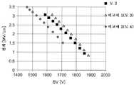
도 2 내지 도 4는, MOSFET가 오프하고 있을 때의 전위 분포를 시뮬레이션에 의해 산출한 결과를 도시하고 있다. 도 2 내지 도 4에 있어서, 파선은, 등전위선을 나타내고 있다. 또한, 도 2는, 실시예 1을 모의한 상대적으로 넓은 경사면(52)을 갖는 MOSFET에 있어서의 전위 분포를 도시하고, 도 3, 도 4는 비교예 1, 2의 MOSFET에 있어서의 전위 분포를 도시하고 있다. 도 3에 도시하는 비교예 1의 MOSFET에서는, 계면(50)이 경사면(52)을 갖지 않고, 바디층(42)과 간격부(44a)의 사이의 계면(50)이 상면(12a)에 대하여 대략 수직으로 신장되어 있다. 도 4에 도시하는 비교예 2의 MOSFET에서는, 계면(50)이 경사면(52)을 갖지만, 경사면(52)이 드리프트층(44)측으로 볼록해지도록 만곡되어 있고, 경사면(52)이 상대적으로 좁다. 바디층(42)이 확산층에 의해 구성되어 있는 경우에는, 불순물을 주입한 단계에서 상대적으로 넓은 경사면(52)을 형성해도, 불순물을 활성화할 때 바디층(42)으로부터 드리프트층(44)측으로 p형 불순물이 확산되므로, 경사면(52)이 드리프트층(44)측을 향하여 만곡된다. 그 결과, 도 4와 같이, 경사면(52)이 상대적으로 좁아진다. 도 3, 도 4에서는, 도 2에 비하여, 간격부(44a)의 상부의 게이트 절연막(28)의 근방에서 등전위선의 간격이 밀하게 되어 있다. 도 2 내지 도 4로부터, 도 2와 같이 경사면(52)이 상대적으로 넓으면, 게이트 절연막(28)에 인가되는 전계가 완화됨을 알 수 있다.Figs. 2 to 4 show results obtained by simulating the potential distribution when the MOSFET is off. Fig. In Figs. 2 to 4, broken lines indicate equipotential lines. 2 shows a potential distribution in a MOSFET having a comparatively wide
또한, 도 5, 도 6은, 도 2의 MOSFET와, 비교예 1, 2(도 3, 도 4)의 MOSFET의 특성을 비교하여 도시하고 있다. 도 5는, 드레인-소스 간 전압 BV와, 온 저항의 관계를 도시하고 있다. 도 6은, 드레인-소스 간 전압 BV와, 산화막에 인가되는 전계의 관계를 도시하고 있다. 도 5로부터, 도 2의 MOSFET는, 비교예 1, 2의 MOSFET와 동등한 온 저항이 얻어짐을 알 수 있다. 또한, 도 6으로부터, 드레인-소스 간 전압이 동등한 경우에는, 도 2의 MOSFET에서는, 비교예 1, 2의 MOSFET보다 게이트 절연막(28)에 인가되는 전계가 낮음을 알 수 있다. 이상의 결과로부터, 상대적으로 넓은 경사면(52)을 갖는 실시예 1의 MOSFET(10)에 따르면, 비교예 1, 2의 MOSFET와 동등한 온 저항을 얻으면서, 비교예 1, 2의 MOSFET보다 게이트 절연막(28)에 인가되는 전계를 억제할 수 있다.5 and 6 show the MOSFET characteristics of the MOSFET of FIG. 2 and the MOSFET of Comparative Examples 1 and 2 (FIG. 3 and FIG. 4) in comparison with each other. FIG. 5 shows the relationship between the drain-source voltage BV and the on-resistance. FIG. 6 shows the relationship between the drain-source voltage BV and the electric field applied to the oxide film. It can be seen from Fig. 5 that the MOSFET shown in Fig. 2 has on-resistance equivalent to that of MOSFETs of Comparative Examples 1 and 2. It can also be seen from FIG. 6 that the electric field applied to the
이어서, 실시예 1의 MOSFET(10)의 제조 방법에 대하여 설명한다. 우선, 도 7에 도시하는 바와 같이, GaN 반도체 기판(12)의 상면(12a)에 개구(60)를 갖는 마스크(58)를 형성한다. 이어서, 개구(60) 내의 GaN 반도체 기판(12)의 상면을 에칭함으로써, 오목부(62)를 형성한다. 이때, 에칭 조건을 조정하여, 오목부(62)의 측면이 GaN 반도체 기판(12)의 상면에 대하여 경사진(보다 상세하게는, 오목부(62)의 단부(62a)로부터 멀어짐에 따라 오목부(62)의 깊이가 깊어지도록 경사진) 경사면(63)으로 되도록, 오목부(62)를 형성한다. 예를 들어, 마스크(58)의 두께를 개구(60)에 가까운 위치일수록 얇게 하고, 가스종, 압력, RF 파워 등의 조건을 조정하여 마스크(58)와 GaN 반도체 기판(12)의 에칭 레이트의 차를 보다 작게 함으로써, 경사면(63)을 형성할 수 있다. 여기서는, 경사면(63)과 GaN 반도체 기판(12)의 상면의 사이의 각도 θ가, 60°미만으로 되도록, 오목부(62)를 형성한다.Next, a method of manufacturing the
이어서, 마스크(58)를 제거하고, 도 8에 도시하는 바와 같이, 에피택셜 성장에 의해, GaN 반도체 기판(12)의 상면과 오목부(62) 내에, p형의 GaN 반도체층인 바디층(42)을 에피택셜 성장시킨다. 이하에서는, 드리프트층(44)과 바디층(42)을 포함하는 GaN 반도체층 전체를, GaN 반도체 기판(12)이라고 한다.Subsequently, the
이어서, GaN 반도체 기판(12)의 상면(즉, 바디층(42)의 표면)을 CMP(Chemical Mechanical Polishing)에 의해 연마한다. 여기서는, 도 9에 도시하는 바와 같이, 드리프트층(44)의 간격부(44a)를 GaN 반도체 기판(12)의 상면에 노출시킨다. 또한, 오목부(62) 내에, 바디층(42)을 잔존시킨다.Then, the upper surface of the GaN semiconductor substrate 12 (that is, the surface of the body layer 42) is polished by CMP (Chemical Mechanical Polishing). Here, as shown in Fig. 9, the
이어서, 도 10에 도시하는 바와 같이, 바디층(42)의 일부에 선택적으로 n형 불순물 이온을 주입함으로써, 소스층(40)을 형성한다.Then, as shown in Fig. 10, the
이어서, 도 11에 도시하는 바와 같이, 게이트 절연막(28)을 형성한다. 게이트 절연막(28)은, 바디층(42) 근방의 소스층(40)의 표면과, 소스층(40)과 간격부(44a)의 사이의 바디층(42)의 표면과, 간격부(44a)의 표면에 걸치는 범위를 덮도록 형성된다. 이어서, 도 11에 도시하는 바와 같이, 게이트 절연막(28)의 상면 전체를 덮도록 게이트 전극(26)을 형성한다. 그 후, 층간 절연막(24), 콘택트 플러그(22), 상부 전극(20) 및 하부 전극(30)을 형성함으로써, 도 1의 MOSFET(10)가 완성된다.Then, as shown in Fig. 11, a
이상에 설명한 바와 같이, 실시예 1의 MOSFET(10)에서는, 바디층(42)이 에피택셜층이다. 이 때문에, 바디층(42)을 형성할 때, 바디층(42)으로부터 드리프트층(44)으로 p형 불순물이 거의 확산되지 않는다. 따라서, 계면(50)을 오목부(62)와 대략 동일한 형상으로 할 수 있다. 이 때문에, 바디층(42)을 에피택셜층으로 함으로써, 경사면(52)을 원하는 형상으로 할 수 있다. 즉, 바디층(42)을 에피택셜층으로 함으로써, 경사면(52)의 만곡을 억제하여, 경사면(52)을 상대적으로 넓게 할 수 있다. 따라서, 본 실시예 1의 MOSFET(10)는, 게이트 절연막(28)에 인가되는 전계를 효과적으로 완화할 수 있다.As described above, in the
도 12에 도시하는 실시예 2의 MOSFET는, 바디층(42)과 간격부(44a)(즉, 드리프트층(44))의 사이의 계면(50)이, 표층부 계면(53)과 경사면(52)을 갖는다는 점에서 실시예 1의 MOSFET(10)와는 상이하다. 실시예 2의 MOSFET의 그 밖의 구성은, 실시예 1의 MOSFET(10)와 동등하다. 표층부 계면(53)은, 계면(50) 중 상면(12a) 근방에 위치하는 부분이다. 표층부 계면(53)과 상면(12a)의 사이의 각도 θ1은, 80°이상 90°이하이다. 즉, 표층부 계면(53)은, 상면(12a)으로부터 하측 방향으로 대략 수직으로 신장되어 있다. 경사면(52)은, 표층부 계면(53)의 하측에 배치되어 있다. 경사면(52)의 상단이, 표층부 계면(53)의 하단에 접속되어 있다. 경사면(52)은, 바디층(42)의 단부(42a)로부터 횡방향을 따라 이격됨에 따라 바디층(42)의 깊이가 깊어지도록 상면(12a)에 대하여 경사져 있다. 경사면(52)과 상면(12a)의 사이의 각도 θ2는, 60°미만이다.The MOSFET of the second embodiment shown in Fig. 12 is different from the MOSFET of the second embodiment shown in Fig. 12 in that the
실시예 2의 MOSFET에서는, 바디층(42)이 에피택셜층이므로, 경사면(52)이 상대적으로 넓다. 따라서, 실시예 2의 MOSFET에서는, 게이트 절연막(28)에 인가되는 전계가 완화된다.In the MOSFET of the second embodiment, since the
또한, 실시예 2의 MOSFET에서는, 경사면(52)의 상부에 표층부 계면(53)이 마련되어 있다. 이 때문에, 실시예 1과 실시예 2에서 간격부(44a)의 폭을 동일하게 한 경우에 있어서, 경사면(52)에서부터 소스층(40)까지의 거리가 실시예 1보다 실시예 2에서 길어진다. MOSFET가 온되어 있는 상태에서는, 경사면(52)을 포함하는 계면(50)의 주변에 국소적으로 공핍층이 발생하고 있다. 실시예 2의 MOSFET에서는, 온 상태에 있어서 경사면(52)의 주변에 발생하고 있는 공핍층과 소스층(40)의 사이의 거리가, 실시예 1의 MOSFET(10)보다 넓어진다. 이 때문에, 실시예 2의 MOSFET에서는, 단채널 효과가 발생하기 어렵다. 따라서, 실시예 2의 구조에 따르면, 단채널 효과에 의한 게이트 역치의 변동을 보다 억제할 수 있다.In the MOSFET of the second embodiment, the
또한, 실시예 2와 같이 상면(12a)에 대하여 대략 수직으로 신장하는 표층부 계면(53)이 형성되어 있으면, 양산될 때 MOSFET의 사이에 있어서, 간격부(44a)의 상면(12a)에 있어서의 폭(즉, 실시예 2에 있어서, 간격부(44a)의 양측에 위치하는 표층부 계면(53)의 사이의 폭)에 변동이 발생하기 어렵다. 간격부(44a)의 폭이 상대적으로 넓으면, 간격부(44a)의 상부의 게이트 절연막(28)에 높은 전계가 보다 인가되기 쉬워진다. 실시예 2의 MOSFET 구조에 따르면, 간격부(44a)의 폭의 변동이 억제되므로, 게이트 절연막(28)에 인가되는 전계를 안정되게 억제하는 것이 가능하게 된다.When the
실시예 2의 MOSFET는, 도 13에 도시하는 형상의 오목부(62)를 형성하고, 그 후, 실시예 1과 마찬가지의 공정을 실시함으로써 제조할 수 있다. 도 13에 도시하는 형상의 오목부(62)는, 최초로, 실시예 1과 마찬가지로 도 7과 같이 오목부(62)를 형성하고, 그 후에 균일하게 GaN 반도체 기판(12)의 두께 방향을 따라 에칭이 진행되는 조건에서 오목부(62)를 더 에칭함으로써 얻을 수 있다.The MOSFET of the second embodiment can be manufactured by forming the
또한, 상술한 실시예 1, 2에서는, MOSFET에 대하여 설명하였지만, IGBT에 본 명세서에 개시된 기술을 적용해도 된다. 하부 전극(30)과 드리프트층(44)의 사이에 p형층을 추가함으로써, IGBT의 구조를 얻을 수 있다.Although the MOSFETs have been described in the first and second embodiments, the techniques disclosed in this specification may be applied to the IGBT. By adding a p-type layer between the
또한, 상술한 실시예 1, 2에서는, 반도체 기판으로서 GaN 반도체 기판을 사용하였다. 그러나, SiC나 Si를 주성분으로 하는 반도체 기판을 갖는 스위칭 소자에, 본 명세서에 개시된 기술을 적용해도 된다. 단, 본 명세서에 개시된 기술은, GaN이나 SiC 등의 불순물의 확산을 제어하는 것이 곤란한 반도체 기판을 사용하는 경우에 특히 유효하다.In
실시예의 구성 요소와 청구항의 구성 요소의 관계에 대하여 설명한다. 실시예의 드리프트층(44)은, 제1 n형 반도체층의 일례이다. 실시예의 소스층(40)은, 제2 n형 반도체층의 일례이다.The relationship between the components of the embodiment and the components of the claims will be described. The
본 개시의 기술 요소에 대하여, 이하에 설명한다.The technical elements of this disclosure will be described below.
본 개시의 일례의 스위칭 소자에서는, 제1 n형 반도체층과 바디층의 계면이, 게이트 전극의 하부에 있어서 반도체 기판의 표면으로부터 하측 방향으로 신장되고, 반도체 기판의 표면에 대한 각도가 80°이상 90°이하인 표층부 계면을 갖는다. 경사면이, 표층부 계면의 하측에 위치한다. 경사면의 반도체 기판의 표면에 대한 각도가 60°미만이다.In an example of the switching device of this disclosure, the interface between the first n-type semiconductor layer and the body layer is extended downward from the surface of the semiconductor substrate at the lower portion of the gate electrode, and the angle with respect to the surface of the semiconductor substrate is at least 80 And has a surface layer interface of 90 DEG or less. The inclined surface is located on the lower side of the surface layer interface. The angle of the inclined surface with respect to the surface of the semiconductor substrate is less than 60 degrees.
또한, 본 명세서에 있어서, 반도체 기판의 표면에 대한 계면(즉, 표층부 계면 또는 경사면)의 각도는, 바디층 내에 있어서 계측되는 각도를 의미한다.In this specification, the angle of the interface (that is, the surface layer interface or the inclined surface) with respect to the surface of the semiconductor substrate means the angle measured in the body layer.
이상, 실시 형태에 대하여 상세하게 설명하였지만, 이들은 예시에 지나지 않으며, 특허청구범위를 한정하는 것은 아니다. 특허청구범위에 기재된 기술에는, 이상에 예시한 구체예를 여러 가지로 변형, 변경한 것이 포함된다. 본 명세서 또는 도면에 설명한 기술 요소는, 단독 혹은 각종 조합에 의해 기술 유용성을 발휘하는 것이며, 출원 시 청구항에 기재된 조합에 한정되는 것은 아니다. 또한, 본 명세서 또는 도면에 예시된 기술은 복수 목적을 동시에 달성하는 것이며, 그 중 하나의 목적을 달성하는 것 자체로 기술 유용성을 갖는 것이다.Although the embodiments have been described in detail above, they are merely illustrative and do not limit the claims. The techniques described in the claims include various modifications and changes to the specific examples described above. The technical elements described in this specification or the drawings exert their technical usefulness individually or in various combinations and are not limited to the combinations described in the claims at the time of filing. Further, the techniques exemplified in the present specification or drawings are intended to achieve a plurality of objectives at the same time, and achieving one of the purposes of the present invention is technological usability.
Claims (5)
Translated fromKorean반도체 기판(12)의 표면에 노출되어 있는 제1 n형 반도체층(44)과,
상기 반도체 기판(12)의 상기 표면에 노출되어 있는 에피택셜층에 의해 구성되어 있는 p형의 바디층(42)과,
상기 반도체 기판(12)의 상기 표면에 노출되어 있고, 상기 바디층(42)에 의해 상기 제1 n형 반도체층(44)으로부터 분리되어 있는 제2 n형 반도체층(40)을 갖는 반도체 기판(12);
상기 제1 n형 반도체층(44)의 표면과, 상기 제1 n형 반도체층(44)과 상기 제2 n형 반도체층(40)의 사이의 상기 바디층(42)의 표면과, 상기 제2 n형 반도체층(40)의 표면에 걸치는 범위를 덮는 게이트 절연막(28); 및
상기 게이트 절연막(28)을 개재시켜, 상기 제1 n형 반도체층(44)과 상기 제2 n형 반도체층(40)의 사이의 상기 바디층(42)에 대향하는 게이트 전극(26)을;
포함하고,
상기 제1 n형 반도체층(44)과 상기 바디층(42)의 계면(50)이 경사면(52, 63)을 갖고, 상기 경사면(52, 63)은 상기 바디층(42)의 단부(42a)로부터 횡방향으로 이격됨에 따라 상기 바디층(42)의 깊이가 깊어지도록 경사진 경사면(52, 63)을 갖고, 상기 경사면(52, 63)이, 상기 게이트 전극(26)의 하부에 배치되어 있고,
상기 계면(50)이, 상기 게이트 전극(26)의 하부에 있어서 상기 반도체 기판(12)의 상기 표면으로부터 하측 방향으로 신장되고, 상기 반도체 기판(12)의 상기 표면에 대한 각도가 80°이상 90°이하인 표층부 계면(53)을 갖고,
상기 경사면(52, 63)이, 상기 표층부 계면(53)의 하측에 위치하고,
상기 경사면(52, 63)의 상기 반도체 기판(12)의 상기 표면에 대한 각도가 60°미만인, 스위칭 소자(10).In the switching element 10,
A first n-type semiconductor layer 44 exposed on the surface of the semiconductor substrate 12,
A p-type body layer 42 composed of an epitaxial layer exposed on the surface of the semiconductor substrate 12,
And a second n-type semiconductor layer (40) exposed on the surface of the semiconductor substrate (12) and separated from the first n-type semiconductor layer (44) by the body layer (42) 12);
The surface of the first n-type semiconductor layer 44 and the surface of the body layer 42 between the first n-type semiconductor layer 44 and the second n-type semiconductor layer 40, A gate insulating film 28 covering a range covering the surface of the 2 < n > -type semiconductor layer 40; And
A gate electrode 26 opposing the body layer 42 between the first n-type semiconductor layer 44 and the second n-type semiconductor layer 40 with the gate insulating film 28 interposed therebetween;
Including,
The interface 50 between the first n-type semiconductor layer 44 and the body layer 42 has inclined planes 52 and 63 and the inclined planes 52 and 63 are parallel to the ends 42a of the body layer 42 And the inclined surfaces 52 and 63 are disposed at a lower portion of the gate electrode 26 so that the depth of the body layer 42 is increased as the body layer 42 is laterally spaced from the gate electrode 26. [ However,
Wherein the interface (50) extends downward from the surface of the semiconductor substrate (12) at a lower portion of the gate electrode (26), and the angle of the semiconductor substrate (12) Deg.] Or less,
The inclined surfaces (52, 63) are positioned below the surface layer interface (53)
Wherein an angle of the slope (52, 63) to the surface of the semiconductor substrate (12) is less than 60 degrees.
게이트 절연막(28)과, 상기 게이트 절연막(28)을 개재시켜, 상기 제1 n형 반도체층(44)과 상기 제2 n형 반도체층(40)의 사이의 상기 바디층(42)에 대향하는 게이트 전극(26)을 구비하는 스위칭 소자(10)의 제조 방법이며,
상기 반도체 기판(12)의 상면에 개구(60)를 갖는 마스크(58)를 형성하고,
상기 개구(60)의 상기 반도체 기판(12)의 상면을 에칭하여 오목부(62)를 형성하고, 상기 에칭에서는 상기 오목부(62)의 측면이 상기 반도체 기판(12)의 상면에 대하여, 상기 오목부(62)의 단부(62a)로부터 횡방향을 향하여 이격됨에 따라 상기 오목부(62)의 깊이가 깊어지도록 경사진 경사면(52, 63)으로 되도록, 상기 오목부(62)를 형성하고,
상기 마스크(58)를 제거하고,
에피택셜 성장에 의해, 상기 반도체 기판(12)의 상면과 상기 오목부(62) 내에, 상기 바디층(42)을 에피택셜 성장시키고,
상기 반도체 기판(12)의 상면을 연마하고,
상기 바디층(42)의 일부에 선택적으로 n형 불순물 이온을 주입하고, 상기 제2 n형 반도체층(40)을 형성하고,
상기 게이트 절연막(28)을, 상기 제1 n형 반도체층(44)의 표면과, 상기 제1 n형 반도체층(44)과 상기 제2 n형 반도체층(40)의 사이의 상기 바디층(42)의 표면과, 상기 제2 n형 반도체층(40)의 표면에 걸치는 범위를 덮도록 형성하고,
상기 게이트 절연막(28)의 상면 전체를 덮도록 상기 게이트 전극(26)을 형성하고,
상기 반도체 기판(12) 표면 및 상기 게이트 전극(26)의 표면을 덮도록 층간 절연막(24)을 형성하고,
상기 층간 절연막(24)에 마련된 콘택트 홀 내에 콘택트 플러그(22)를 형성하고,
상기 층간 절연막(24)의 상면에 상부 전극(20)을 배치하고,
상기 반도체 기판(12) 중 상기 층간 절연막(24)이 형성되는 면과는 반대의 면에 하부 전극(30)을 배치하는
것을 포함하고,
상기 제1 n형 반도체층(44)과 상기 바디층(42)의 계면(50)이, 상기 게이트 전극(26)의 하부에 있어서 상기 반도체 기판(12)의 상기 표면으로부터 하측 방향으로 신장되고, 상기 반도체 기판(12)의 상기 표면에 대한 각도가 80°이상 90°이하인 표층부 계면(53)을 갖고,
상기 경사면(52, 63)이, 상기 표층부 계면(53)의 하측에 위치하고,
상기 경사면(52, 63)의 상기 반도체 기판(12)의 상기 표면에 대한 각도가 60°미만인, 스위칭 소자(10)의 제조 방법.A first n-type semiconductor layer 44 exposed on the surface of the semiconductor substrate 12; a p-type body layer 42; A second n-type semiconductor layer (40) separated from the first n-type semiconductor layer (44) by the second n-type semiconductor layer (42)
A gate insulating film 28 is formed on the first n-type semiconductor layer 40 and a gate insulating film 28 is formed between the first n-type semiconductor layer 44 and the second n-type semiconductor layer 40, A method of manufacturing a switching device (10) having a gate electrode (26)
A mask 58 having an opening 60 is formed on the upper surface of the semiconductor substrate 12,
The recessed portion 62 is formed by etching the upper surface of the semiconductor substrate 12 of the opening 60 so that the side surface of the recessed portion 62 is etched with respect to the upper surface of the semiconductor substrate 12, The concave portion 62 is formed so as to be inclined surfaces 52 and 63 inclined so as to deepen the depth of the concave portion 62 as the concave portion 62 is laterally spaced from the end portion 62a of the concave portion 62,
The mask 58 is removed,
Epitaxially growing the body layer (42) in the recessed portion (62) and the upper surface of the semiconductor substrate (12)
The upper surface of the semiconductor substrate 12 is polished,
Type impurity ions are selectively implanted into a part of the body layer 42 to form the second n-type semiconductor layer 40,
The gate insulating film 28 is formed on the surface of the first n-type semiconductor layer 44 and the surface of the body layer between the first n-type semiconductor layer 44 and the second n-type semiconductor layer 40 42 and the surface of the second n-type semiconductor layer 40,
The gate electrode 26 is formed so as to cover the entire upper surface of the gate insulating film 28,
An interlayer insulating film 24 is formed so as to cover the surface of the semiconductor substrate 12 and the surface of the gate electrode 26,
A contact plug 22 is formed in a contact hole provided in the interlayer insulating film 24,
An upper electrode 20 is disposed on the upper surface of the interlayer insulating film 24,
The lower electrode 30 is disposed on the surface of the semiconductor substrate 12 opposite to the surface on which the interlayer insulating film 24 is formed
≪ / RTI >
The interface 50 between the first n-type semiconductor layer 44 and the body layer 42 extends downward from the surface of the semiconductor substrate 12 below the gate electrode 26, And a surface layer interface (53) having an angle with respect to the surface of the semiconductor substrate (12) of 80 ° or more and 90 ° or less,
The inclined surfaces (52, 63) are positioned below the surface layer interface (53)
Wherein an angle of the inclined surfaces (52, 63) to the surface of the semiconductor substrate (12) is less than 60 degrees.
Applications Claiming Priority (2)
| Application Number | Priority Date | Filing Date | Title |
|---|---|---|---|
| JPJP-P-2016-253898 | 2016-12-27 | ||
| JP2016253898AJP6616280B2 (en) | 2016-12-27 | 2016-12-27 | Switching element |
Publications (2)
| Publication Number | Publication Date |
|---|---|
| KR20180076320A KR20180076320A (en) | 2018-07-05 |
| KR101987562B1true KR101987562B1 (en) | 2019-06-10 |
Family
ID=60673152
Family Applications (1)
| Application Number | Title | Priority Date | Filing Date |
|---|---|---|---|
| KR1020170177063AActiveKR101987562B1 (en) | 2016-12-27 | 2017-12-21 | Switching element and method of manufacturing switching element |
Country Status (10)
| Country | Link |
|---|---|
| US (1) | US10312362B2 (en) |
| EP (1) | EP3352203B1 (en) |
| JP (1) | JP6616280B2 (en) |
| KR (1) | KR101987562B1 (en) |
| CN (1) | CN108321204B (en) |
| BR (1) | BR102017026277B1 (en) |
| CA (1) | CA2988371C (en) |
| MY (1) | MY191814A (en) |
| RU (1) | RU2665798C1 (en) |
| TW (1) | TWI664729B (en) |
Families Citing this family (3)
| Publication number | Priority date | Publication date | Assignee | Title |
|---|---|---|---|---|
| JP6549552B2 (en)* | 2016-12-27 | 2019-07-24 | トヨタ自動車株式会社 | Method of manufacturing switching element |
| JP6616280B2 (en) | 2016-12-27 | 2019-12-04 | トヨタ自動車株式会社 | Switching element |
| KR102767850B1 (en)* | 2019-11-19 | 2025-02-14 | 삼성전자주식회사 | Semiconductor device, transistor including the same and method of manufacturing the transistor |
Citations (3)
| Publication number | Priority date | Publication date | Assignee | Title |
|---|---|---|---|---|
| JP2002158353A (en)* | 2000-09-11 | 2002-05-31 | Toshiba Corp | MOS field effect transistor |
| JP2009147381A (en)* | 2003-03-28 | 2009-07-02 | Mitsubishi Electric Corp | Manufacturing method of vertical MOSFET using SiC |
| US20160043199A1 (en)* | 2014-08-07 | 2016-02-11 | Kabushiki Kaisha Toshiba | Method of manufacturing semiconductor device |
Family Cites Families (29)
| Publication number | Priority date | Publication date | Assignee | Title |
|---|---|---|---|---|
| US5528058A (en)* | 1986-03-21 | 1996-06-18 | Advanced Power Technology, Inc. | IGBT device with platinum lifetime control and reduced gaw |
| JP3206727B2 (en)* | 1997-02-20 | 2001-09-10 | 富士電機株式会社 | Silicon carbide vertical MOSFET and method of manufacturing the same |
| JP3180895B2 (en)* | 1997-08-18 | 2001-06-25 | 富士電機株式会社 | Method for manufacturing silicon carbide semiconductor device |
| JP2000106428A (en) | 1998-09-28 | 2000-04-11 | Toshiba Corp | Semiconductor device |
| US6365932B1 (en)* | 1999-08-20 | 2002-04-02 | Denso Corporation | Power MOS transistor |
| JP3964811B2 (en)* | 2002-07-09 | 2007-08-22 | 株式会社東芝 | Semiconductor device and manufacturing method thereof |
| JP4645034B2 (en) | 2003-02-06 | 2011-03-09 | 株式会社豊田中央研究所 | Semiconductor device having group III nitride semiconductor |
| JP2004319964A (en) | 2003-03-28 | 2004-11-11 | Mitsubishi Electric Corp | Semiconductor device and manufacturing method thereof |
| JP2007005764A (en)* | 2005-05-27 | 2007-01-11 | Toyota Motor Corp | Semiconductor device and manufacturing method thereof |
| JP2007281086A (en)* | 2006-04-04 | 2007-10-25 | Sumitomo Electric Ind Ltd | Insulated gate bipolar transistor and method of making an insulated gate bipolar transistor |
| WO2007122646A1 (en)* | 2006-04-21 | 2007-11-01 | Stmicroelectronics S.R.L. | Process for manufacturing a power semiconductor device and corresponding power semiconductor device |
| US7629616B2 (en) | 2007-02-28 | 2009-12-08 | Cree, Inc. | Silicon carbide self-aligned epitaxial MOSFET for high powered device applications |
| JP2009091175A (en) | 2007-10-04 | 2009-04-30 | Sumitomo Electric Ind Ltd | GaN epitaxial substrate, semiconductor device, GaN epitaxial substrate, and manufacturing method of semiconductor device |
| US7633121B2 (en)* | 2007-10-31 | 2009-12-15 | Force-Mos Technology Corp. | Trench MOSFET with implanted drift region |
| JP4640439B2 (en)* | 2008-04-17 | 2011-03-02 | 株式会社デンソー | Silicon carbide semiconductor device |
| RU2402105C1 (en)* | 2009-08-03 | 2010-10-20 | Закрытое акционерное общество "Научно-производственная фирма Микран" | Vertical field transistor |
| JP5520024B2 (en)* | 2009-12-09 | 2014-06-11 | ルネサスエレクトロニクス株式会社 | Semiconductor device and manufacturing method thereof |
| US8786010B2 (en)* | 2011-04-27 | 2014-07-22 | Fairchild Semiconductor Corporation | Superjunction structures for power devices and methods of manufacture |
| JP5524905B2 (en)* | 2011-05-17 | 2014-06-18 | 株式会社神戸製鋼所 | Al alloy film for power semiconductor devices |
| US8963218B2 (en)* | 2011-09-30 | 2015-02-24 | Maxim Integrated Products, Inc. | Dual-gate VDMOS device |
| US9196709B2 (en)* | 2013-02-01 | 2015-11-24 | Taiwan Semiconductor Manufacturing Company, Ltd. | Methods for forming semiconductor regions in trenches |
| US9070765B2 (en)* | 2013-02-06 | 2015-06-30 | Infineon Technologies Ag | Semiconductor device with low on resistance and high breakdown voltage |
| US9799734B2 (en)* | 2013-06-17 | 2017-10-24 | Hitachi, Ltd. | Semiconductor device and manufacturing method for same, as well as power conversion device |
| KR20150014641A (en) | 2013-07-30 | 2015-02-09 | 서울반도체 주식회사 | Gallium nitnide based field effect transistor and method of fabricating the same |
| US9111919B2 (en)* | 2013-10-03 | 2015-08-18 | Cree, Inc. | Field effect device with enhanced gate dielectric structure |
| US9496149B2 (en) | 2014-04-14 | 2016-11-15 | Taiwan Semiconductor Manufacturing Company, Ltd. | Semiconductor devices and methods for manufacturing the same |
| JP2017126610A (en) | 2016-01-12 | 2017-07-20 | トヨタ自動車株式会社 | Switching element |
| JP6549552B2 (en) | 2016-12-27 | 2019-07-24 | トヨタ自動車株式会社 | Method of manufacturing switching element |
| JP6616280B2 (en) | 2016-12-27 | 2019-12-04 | トヨタ自動車株式会社 | Switching element |
- 2016
- 2016-12-27JPJP2016253898Apatent/JP6616280B2/enactiveActive
- 2017
- 2017-12-06USUS15/833,938patent/US10312362B2/enactiveActive
- 2017-12-06BRBR102017026277-4Apatent/BR102017026277B1/enactiveIP Right Grant
- 2017-12-08RURU2017142945Apatent/RU2665798C1/enactive
- 2017-12-08MYMYPI2017704728Apatent/MY191814A/enunknown
- 2017-12-08TWTW106143067Apatent/TWI664729B/enactive
- 2017-12-12EPEP17206608.6Apatent/EP3352203B1/enactiveActive
- 2017-12-12CACA2988371Apatent/CA2988371C/enactiveActive
- 2017-12-20CNCN201711384307.6Apatent/CN108321204B/enactiveActive
- 2017-12-21KRKR1020170177063Apatent/KR101987562B1/enactiveActive
Patent Citations (3)
| Publication number | Priority date | Publication date | Assignee | Title |
|---|---|---|---|---|
| JP2002158353A (en)* | 2000-09-11 | 2002-05-31 | Toshiba Corp | MOS field effect transistor |
| JP2009147381A (en)* | 2003-03-28 | 2009-07-02 | Mitsubishi Electric Corp | Manufacturing method of vertical MOSFET using SiC |
| US20160043199A1 (en)* | 2014-08-07 | 2016-02-11 | Kabushiki Kaisha Toshiba | Method of manufacturing semiconductor device |
Also Published As
| Publication number | Publication date |
|---|---|
| US10312362B2 (en) | 2019-06-04 |
| CN108321204B (en) | 2021-04-09 |
| JP2018107336A (en) | 2018-07-05 |
| CA2988371A1 (en) | 2018-06-27 |
| RU2665798C1 (en) | 2018-09-04 |
| TW201826539A (en) | 2018-07-16 |
| BR102017026277B1 (en) | 2023-03-07 |
| CN108321204A (en) | 2018-07-24 |
| BR102017026277A2 (en) | 2018-07-17 |
| EP3352203B1 (en) | 2021-05-12 |
| US20180182883A1 (en) | 2018-06-28 |
| KR20180076320A (en) | 2018-07-05 |
| JP6616280B2 (en) | 2019-12-04 |
| EP3352203A1 (en) | 2018-07-25 |
| CA2988371C (en) | 2019-07-02 |
| TWI664729B (en) | 2019-07-01 |
| MY191814A (en) | 2022-07-18 |
Similar Documents
| Publication | Publication Date | Title |
|---|---|---|
| CN107996003B (en) | Insulated gate switching device and method of manufacturing the same | |
| US11476360B2 (en) | Semiconductor device and method for manufacturing the same | |
| USRE47641E1 (en) | Semiconductor device with super junction region | |
| KR102080129B1 (en) | Nitride semiconductor apparatus and method of manufacturing nitride semiconductor apparatus | |
| KR101987562B1 (en) | Switching element and method of manufacturing switching element | |
| JP2021082713A (en) | Semiconductor device | |
| CN119054083A (en) | Semiconductor device and method for manufacturing the same | |
| JP7331653B2 (en) | Semiconductor device manufacturing method | |
| JP7192504B2 (en) | semiconductor equipment | |
| JP7127315B2 (en) | Silicon carbide semiconductor device and manufacturing method thereof | |
| JP7188971B2 (en) | Semiconductor device and its manufacturing method | |
| JP6988261B2 (en) | Nitride semiconductor equipment | |
| JP7380236B2 (en) | semiconductor equipment | |
| US20240128371A1 (en) | Semiconductor device and method of manufacturing the same | |
| KR20190100012A (en) | Power Semiconductor with P Shield Structure Implemented by Multiple Epi-Growth Method and Fabrication Method | |
| JP7115145B2 (en) | Semiconductor device manufacturing method | |
| JP2024029440A (en) | Semiconductor device and its manufacturing method | |
| WO2013051343A1 (en) | Silicon carbide semiconductor device and method for producing same |
Legal Events
| Date | Code | Title | Description |
|---|---|---|---|
| A201 | Request for examination | ||
| PA0109 | Patent application | Patent event code:PA01091R01D Comment text:Patent Application Patent event date:20171221 | |
| PA0201 | Request for examination | ||
| PG1501 | Laying open of application | ||
| E902 | Notification of reason for refusal | ||
| PE0902 | Notice of grounds for rejection | Comment text:Notification of reason for refusal Patent event date:20181029 Patent event code:PE09021S01D | |
| E701 | Decision to grant or registration of patent right | ||
| PE0701 | Decision of registration | Patent event code:PE07011S01D Comment text:Decision to Grant Registration Patent event date:20190522 | |
| GRNT | Written decision to grant | ||
| PR0701 | Registration of establishment | Comment text:Registration of Establishment Patent event date:20190603 Patent event code:PR07011E01D | |
| PR1002 | Payment of registration fee | Payment date:20190603 End annual number:3 Start annual number:1 | |
| PG1601 | Publication of registration | ||
| PR1001 | Payment of annual fee | Payment date:20220530 Start annual number:4 End annual number:4 |