KR101987424B1 - Pixel, diplay device comprising the pixel and driving method of the diplay device - Google Patents
Pixel, diplay device comprising the pixel and driving method of the diplay deviceDownload PDFInfo
- Publication number
- KR101987424B1 KR101987424B1KR1020120137231AKR20120137231AKR101987424B1KR 101987424 B1KR101987424 B1KR 101987424B1KR 1020120137231 AKR1020120137231 AKR 1020120137231AKR 20120137231 AKR20120137231 AKR 20120137231AKR 101987424 B1KR101987424 B1KR 101987424B1
- Authority
- KR
- South Korea
- Prior art keywords
- pixels
- pixel
- compensation
- voltage
- data
- Prior art date
- Legal status (The legal status is an assumption and is not a legal conclusion. Google has not performed a legal analysis and makes no representation as to the accuracy of the status listed.)
- Active
Links
- 238000000034methodMethods0.000titleclaimsdescription51
- 238000012545processingMethods0.000claimsabstractdescription5
- 239000003990capacitorSubstances0.000claimsdescription27
- 238000012546transferMethods0.000claimsdescription5
- 230000008569processEffects0.000description22
- 238000010586diagramMethods0.000description9
- 230000006866deteriorationEffects0.000description5
- 230000010354integrationEffects0.000description5
- 230000004044responseEffects0.000description5
- 239000003086colorantSubstances0.000description4
- 238000013461designMethods0.000description4
- 230000008901benefitEffects0.000description3
- 238000003491arrayMethods0.000description2
- 238000004519manufacturing processMethods0.000description2
- 101100222172Mus musculus Cst10 geneProteins0.000description1
- 230000003213activating effectEffects0.000description1
- 230000008859changeEffects0.000description1
- 239000000470constituentSubstances0.000description1
- 238000012937correctionMethods0.000description1
- 101150037603cst-1 geneProteins0.000description1
- 230000007547defectEffects0.000description1
- 230000000593degrading effectEffects0.000description1
- 239000000463materialSubstances0.000description1
- 238000007781pre-processingMethods0.000description1
Images


Classifications
- G—PHYSICS
- G09—EDUCATION; CRYPTOGRAPHY; DISPLAY; ADVERTISING; SEALS
- G09G—ARRANGEMENTS OR CIRCUITS FOR CONTROL OF INDICATING DEVICES USING STATIC MEANS TO PRESENT VARIABLE INFORMATION
- G09G3/00—Control arrangements or circuits, of interest only in connection with visual indicators other than cathode-ray tubes
- G09G3/20—Control arrangements or circuits, of interest only in connection with visual indicators other than cathode-ray tubes for presentation of an assembly of a number of characters, e.g. a page, by composing the assembly by combination of individual elements arranged in a matrix no fixed position being assigned to or needed to be assigned to the individual characters or partial characters
- G09G3/22—Control arrangements or circuits, of interest only in connection with visual indicators other than cathode-ray tubes for presentation of an assembly of a number of characters, e.g. a page, by composing the assembly by combination of individual elements arranged in a matrix no fixed position being assigned to or needed to be assigned to the individual characters or partial characters using controlled light sources
- G09G3/30—Control arrangements or circuits, of interest only in connection with visual indicators other than cathode-ray tubes for presentation of an assembly of a number of characters, e.g. a page, by composing the assembly by combination of individual elements arranged in a matrix no fixed position being assigned to or needed to be assigned to the individual characters or partial characters using controlled light sources using electroluminescent panels
- G09G3/32—Control arrangements or circuits, of interest only in connection with visual indicators other than cathode-ray tubes for presentation of an assembly of a number of characters, e.g. a page, by composing the assembly by combination of individual elements arranged in a matrix no fixed position being assigned to or needed to be assigned to the individual characters or partial characters using controlled light sources using electroluminescent panels semiconductive, e.g. using light-emitting diodes [LED]
- G09G3/3208—Control arrangements or circuits, of interest only in connection with visual indicators other than cathode-ray tubes for presentation of an assembly of a number of characters, e.g. a page, by composing the assembly by combination of individual elements arranged in a matrix no fixed position being assigned to or needed to be assigned to the individual characters or partial characters using controlled light sources using electroluminescent panels semiconductive, e.g. using light-emitting diodes [LED] organic, e.g. using organic light-emitting diodes [OLED]
- G09G3/3225—Control arrangements or circuits, of interest only in connection with visual indicators other than cathode-ray tubes for presentation of an assembly of a number of characters, e.g. a page, by composing the assembly by combination of individual elements arranged in a matrix no fixed position being assigned to or needed to be assigned to the individual characters or partial characters using controlled light sources using electroluminescent panels semiconductive, e.g. using light-emitting diodes [LED] organic, e.g. using organic light-emitting diodes [OLED] using an active matrix
- G—PHYSICS
- G09—EDUCATION; CRYPTOGRAPHY; DISPLAY; ADVERTISING; SEALS
- G09G—ARRANGEMENTS OR CIRCUITS FOR CONTROL OF INDICATING DEVICES USING STATIC MEANS TO PRESENT VARIABLE INFORMATION
- G09G3/00—Control arrangements or circuits, of interest only in connection with visual indicators other than cathode-ray tubes
- G09G3/20—Control arrangements or circuits, of interest only in connection with visual indicators other than cathode-ray tubes for presentation of an assembly of a number of characters, e.g. a page, by composing the assembly by combination of individual elements arranged in a matrix no fixed position being assigned to or needed to be assigned to the individual characters or partial characters
- G09G3/22—Control arrangements or circuits, of interest only in connection with visual indicators other than cathode-ray tubes for presentation of an assembly of a number of characters, e.g. a page, by composing the assembly by combination of individual elements arranged in a matrix no fixed position being assigned to or needed to be assigned to the individual characters or partial characters using controlled light sources
- G09G3/30—Control arrangements or circuits, of interest only in connection with visual indicators other than cathode-ray tubes for presentation of an assembly of a number of characters, e.g. a page, by composing the assembly by combination of individual elements arranged in a matrix no fixed position being assigned to or needed to be assigned to the individual characters or partial characters using controlled light sources using electroluminescent panels
- G—PHYSICS
- G09—EDUCATION; CRYPTOGRAPHY; DISPLAY; ADVERTISING; SEALS
- G09G—ARRANGEMENTS OR CIRCUITS FOR CONTROL OF INDICATING DEVICES USING STATIC MEANS TO PRESENT VARIABLE INFORMATION
- G09G2300/00—Aspects of the constitution of display devices
- G09G2300/08—Active matrix structure, i.e. with use of active elements, inclusive of non-linear two terminal elements, in the pixels together with light emitting or modulating elements
- G09G2300/0809—Several active elements per pixel in active matrix panels
- G09G2300/0842—Several active elements per pixel in active matrix panels forming a memory circuit, e.g. a dynamic memory with one capacitor
- G09G2300/0852—Several active elements per pixel in active matrix panels forming a memory circuit, e.g. a dynamic memory with one capacitor being a dynamic memory with more than one capacitor
- G—PHYSICS
- G09—EDUCATION; CRYPTOGRAPHY; DISPLAY; ADVERTISING; SEALS
- G09G—ARRANGEMENTS OR CIRCUITS FOR CONTROL OF INDICATING DEVICES USING STATIC MEANS TO PRESENT VARIABLE INFORMATION
- G09G2310/00—Command of the display device
- G09G2310/02—Addressing, scanning or driving the display screen or processing steps related thereto
- G09G2310/0243—Details of the generation of driving signals
- G09G2310/0248—Precharge or discharge of column electrodes before or after applying exact column voltages
- G—PHYSICS
- G09—EDUCATION; CRYPTOGRAPHY; DISPLAY; ADVERTISING; SEALS
- G09G—ARRANGEMENTS OR CIRCUITS FOR CONTROL OF INDICATING DEVICES USING STATIC MEANS TO PRESENT VARIABLE INFORMATION
- G09G2320/00—Control of display operating conditions
- G09G2320/04—Maintaining the quality of display appearance
- G09G2320/043—Preventing or counteracting the effects of ageing
- G09G2320/045—Compensation of drifts in the characteristics of light emitting or modulating elements
Landscapes
- Engineering & Computer Science (AREA)
- Physics & Mathematics (AREA)
- Computer Hardware Design (AREA)
- General Physics & Mathematics (AREA)
- Theoretical Computer Science (AREA)
- Control Of El Displays (AREA)
- Control Of Indicators Other Than Cathode Ray Tubes (AREA)
Abstract
Translated fromKoreanDescription
Translated fromKorean본 발명은 표시 장치 및 그 구동 방법에 관한 것으로, 특히 유기 발광 다이오드를 포함하고 디지털 구동을 하는 화소를 포함하는 표시 장치와 그 구동 방법에 관한 것이다.BACKGROUND OF THE
최근 들어 표시 패널이 대형화 및 경량화되고, 3차원 입체 영상이 구현되도록 표시 장치의 고집적화 및 고정밀도가 요구됨과 동시에 정확하고 선명한 영상을 표시하기 위하여 안정적인 구동 방법이 개발되고 있다.2. Description of the Related Art In recent years, display panels have been required to have high integration and high precision so that a display panel becomes larger and lighter, a three-dimensional stereoscopic image is realized, and a stable driving method has been developed to display an accurate and clear image.
종래 표시 장치의 아날로그 방식의 구동은 화소의 회로 소자가 많아져서 대형화 패널에 적용하기 힘들고, 고해상도, 특히 Full HD 대응에 문제가 많다. 종래 화소 회로소자가 7-8개의 트랜지스터와 2-3개의 커패시터 등으로 이루어지기 때문에 레이아웃의 설계와 표시 패널의 제작에 큰 어려움이 있다.Conventionally, the driving of the analog system of the display device is difficult to apply to a large-sized panel due to a large number of circuit elements of the pixel, and there are many problems in high resolution, especially full HD. Conventionally, since the pixel circuit element is composed of 7-8 transistors and 2-3 capacitors, it is difficult to design the layout and manufacture the display panel.
이러한 문제를 해결하기 위하여 대체되는 디지털 구동 방식으로 화소의 회로 소자 개수를 줄여 고집적화와 고해상도에 대응할 수 있도록 개발되었다. 특히 디지털 구동 방식의 화소는 2-3개의 트랜지스터와 1개의 커패시터 등으로 구성되도록 소자 개수를 현저히 줄임으로써 레이아웃 설계와 표시 패널의 제작의 난점을 해결할 수 있었다.In order to solve this problem, digital driving method, which is an alternative, has been developed to reduce the number of circuit elements of a pixel and to cope with high integration and high resolution. Particularly, the number of elements is reduced so that the pixel of the digital driving system is composed of 2-3 transistors and one capacitor, and the difficulties of layout design and manufacturing of the display panel can be solved.
그러나, 이러한 디지털 구동의 화소에서 데이터 신호에 따른 구동 전류를 전달하는 구동 트랜지스터가 선형(linear) 영역에서 동작하기 때문에 유기 발광 소자의 재료, 공정 등의 산포 특성에 따라 전체 패널에서 휘도가 달라지는 문제가 발생된다. 그래서 표시 패널에서 LRU(Long range uniformity), SRU(short range uniformity) 등의 불량이 발현되고 이는 표시 장치의 화질 저하를 유발시킨다.However, since the driving transistor, which transmits the driving current according to the data signal, operates in the linear region in the pixels driven by the digital driving, the problem that the brightness varies in the entire panel depending on the scattering characteristics of the material, . Thus, defects such as LRU (Long Range Uniformity) and SRU (Short Range Uniformity) are displayed on the display panel, which causes deterioration of the image quality of the display device.
따라서, 종래의 아날로그 구동 방식의 화면 표시 특성의 장점을 살리면서도 디지털 구동 방식의 고집적화 및 고해상도 적응성의 장점을 접목시킨 화소 구조와 이를 포함하는 표시 장치 및 그 구동 방법에 대한 개발이 필요하다.Accordingly, there is a need to develop a pixel structure that incorporates the advantages of high integration and high-resolution adaptability of a digital driving method, a display device including the same, and a driving method thereof, while taking advantage of the advantages of the conventional analog driving method.
본 발명의 실시 예를 통해 해결하려는 과제는 디지털 구동 방식에 대응하는 화소 회로의 구조를 제안하여, 고집적화 및 고해상도에 적합한 표시 장치를 제공하면서도, 구동 트랜지스터가 포화 영역에서 동작하게 함으로써, 아날로그 구동 방식의 화질 특성과 동등한 수준의 표시 품질을 제공함에 있다.A problem to be solved by the embodiments of the present invention is to provide a display device suitable for high integration and high resolution by proposing a structure of a pixel circuit corresponding to a digital driving method, And to provide display quality at a level equivalent to the image quality characteristic.
그리고, 본 발명의 해결 과제는 복잡한 화소 회로를 소자 개수를 줄여서 간략히 함으로써 회로의 레이아웃 설계에 유리하고, 유기 발광 소자의 특성 열화에 민감하게 반응하지 않는 화소 구조를 제안함으로써 내구성과 생산성이 향상된 표시 장치를 제공함에 있다.It is another object of the present invention to provide a pixel structure which is advantageous in layout design of a circuit by simplifying a complicated pixel circuit by reducing the number of elements and which does not react sensitively to deterioration of characteristics of an organic light emitting element, .
상기 과제를 해결하기 위한 본 발명의 일 실시 예에 따른 표시 장치는 복수의 데이터 신호를 전달하는 데이터 구동부, 복수의 주사 신호를 생성하여 전달하는 주사 구동부, 상기 복수의 데이터 신호에 따른 구동 전류로 발광하는 복수의 화소를 포함하는 표시 패널, 상기 복수의 데이터 신호에 따른 데이터 전압을 복수의 화소 각각에 인가하기 이전에 상기 복수의 화소 각각에 동시에 소정의 바이어스 전압을 전달하도록 제어하는 보상 제어 신호를 생성하여 전달하는 보상 신호부, 제1 전원전압 및 제2 전원전압의 전압 레벨을 조정하여 공급하는 전원 제어부, 및 외부 영상 신호를 처리하여 상기 복수의 데이터 신호를 생성하고, 상기 데이터 구동부, 주사 구동부, 보상 신호부, 및 전원 제어부의 구동을 각각 제어하는 복수의 구동 제어 신호를 생성하는 타이밍 제어부를 포함한다.According to an aspect of the present invention, there is provided a display device including a data driver for transmitting a plurality of data signals, a scan driver for generating and transmitting a plurality of scan signals, A display panel including a plurality of pixels for generating a plurality of data signals, a compensation control signal for controlling to transmit a predetermined bias voltage to each of the plurality of pixels simultaneously before applying a data voltage according to the plurality of data signals to each of the plurality of pixels A power supply control unit for adjusting and supplying a voltage level of a first power supply voltage and a second power supply voltage for generating a plurality of data signals by processing an external video signal, A compensation signal unit, and a power control unit, And a timing controller.
이때 소정의 바이어스 전압은 상기 복수의 데이터 신호 중 최대 휘도를 표시하는 화이트 전압값으로 설정된다.At this time, the predetermined bias voltage is set to a white voltage value representing the maximum luminance among the plurality of data signals.
그리고 실시 예에 따라서 상기 표시 패널은 상기 복수의 화소 중 복수의 제1 화소를 포함하는 제1 화소 영역 및 상기 복수의 제1 화소를 제외한 나머지 복수의 제2 화소를 포함하는 제2 화소 영역으로 이루어질 수 있다. 이때 상기 보상 신호부는 상기 제1 화소 영역에 포함된 복수의 제1 화소에 연결된 제1 보상 제어선 및 상기 제2 화소 영역에 포함된 복수의 제2 화소에 연결된 제2 보상 제어선을 통해 상기 표시 패널과 연결되고, 상기 제1 보상 제어선과 상기 제2 보상 제어선 각각을 통해 상기 바이어스 전압의 인가를 제어하는 제1 보상 제어 신호 및 제2 보상 제어 신호를 각각 생성하여 전달할 수 있다.The display panel may include a first pixel region including a plurality of first pixels among the plurality of pixels and a second pixel region including a plurality of second pixels except for the plurality of first pixels . The compensation signal unit may include a first compensating control line connected to a plurality of first pixels included in the first pixel region and a second compensating control line connected to a plurality of second pixels included in the second pixel region, And generates and transmits a first compensation control signal and a second compensation control signal for controlling the application of the bias voltage through the first compensation control line and the second compensation control line, respectively.
상기 제1 화소 영역에 포함된 복수의 제1 화소와 상기 제2 화소 영역에 포함된 복수의 제2 화소는 제1 색상 화소, 제2 색상 화소, 제3 색상 화소, 및 상기 제2 색상 화소의 단위로 반복적으로 구성된다.Wherein a plurality of first pixels included in the first pixel region and a plurality of second pixels included in the second pixel region are disposed in a first color pixel, a second color pixel, a third color pixel, and a second color pixel, It is composed repeatedly.
상기 보상 신호부는 상기 표시 패널에 포함된 복수의 화소에 복수의 데이터 신호를 전달하기 이전에 상기 제1 보상 제어 신호 및 상기 제2 보상 제어 신호를 전달한다.The compensation signal unit transfers the first compensation control signal and the second compensation control signal before transferring the plurality of data signals to the plurality of pixels included in the display panel.
상기 바이어스 전압은 상기 데이터 구동부와 상기 복수의 화소 각각에 연결된 복수의 데이터 선을 통해 상기 복수의 화소 각각에 인가될 수 있으나 이에 반드시 제한되는 것은 아니다.The bias voltage may be applied to each of the plurality of pixels through a plurality of data lines connected to the data driver and the plurality of pixels, but is not limited thereto.
상기 복수의 화소 각각은 보상 제어 신호에 따라 스위칭 동작이 제어되는 스위칭 소자를 포함하고, 상기 바이어스 전압은 상기 보상 제어 신호에 대응하여 턴 온 된 스위칭 소자를 통해 인가될 수 있다.Each of the plurality of pixels includes a switching element whose switching operation is controlled in accordance with a compensation control signal, and the bias voltage may be applied through a switching element turned on corresponding to the compensation control signal.
상기 복수의 화소 각각은 상기 보상 제어 신호에 대응하여 상기 바이어스 전압을 복수의 화소 각각의 구동 트랜지스터의 소스 전극에 인가받는 것을 특징으로 한다.And each of the plurality of pixels receives the bias voltage corresponding to the compensation control signal to the source electrode of the driving transistor of each of the plurality of pixels.
상기 전원 제어부는 한 프레임 동안 상기 제1 전원전압을 소정의 하이 레벨 전압으로 공급하고, 상기 한 프레임 중 상기 보상 제어 신호가 전달되는 보상 기간 동안 상기 제2 전원전압을 소정의 하이 레벨 전압으로 공급한다.The power supply controller supplies the first power supply voltage at a predetermined high level voltage for one frame and supplies the second power supply voltage at a predetermined high level voltage during a compensation period in which the compensation control signal is transmitted in one frame .
상기 과제를 해결하기 위한 본 발명의 일 실시 예에 따른 화소는 유기 발광 다이오드, 제1 전원전압 공급선에 전기적으로 연결되어 있고, 상기 유기 발광 다이오드에 구동 전류를 공급하는 구동 트랜지스터, 복수의 주사 신호를 전달하는 복수의 주사선 중 대응하는 주사선에 연결되어 대응하는 주사 신호에 따라 복수의 데이터 신호 중 대응하는 데이터 신호에 따른 데이터 전압을 상기 구동 트랜지스터의 게이트 전극에 전달하는 스위칭 트랜지스터, 상기 제1 전원전압 공급선과 상기 구동 트랜지스터 사이에 연결되어 상기 한 프레임 중 보상 기간 동안 소정의 바이어스 전압을 전달받는 보상 트랜지스터, 상기 데이터 전압을 전달하는 데이터 선에 연결되어 상기 보상 기간 동안 보상 제어 신호에 응답하여 상기 데이터 선을 통해 상기 바이어스 전압을 보상 트랜지스터의 게이트 전극에 전달하는 제어 트랜지스터, 상기 보상 트랜지스터의 게이트 전극에 연결되어 있는 보상 커패시터, 및 상기 구동 트랜지스터의 게이트 전극에 연결되어 있는 저장 커패시터를 포함한다.According to an aspect of the present invention, there is provided a pixel comprising: an organic light emitting diode; a driving transistor electrically connected to a first power supply voltage supply line and supplying a driving current to the organic light emitting diode; A switching transistor connected to a corresponding one of the plurality of scanning lines to transmit a data voltage corresponding to a corresponding one of the plurality of data signals according to a corresponding scanning signal to a gate electrode of the driving transistor, A compensating transistor connected between the driving transistor and the driving transistor and receiving a predetermined bias voltage during a compensating period of the frame, a data line connected to the data line for transmitting the data voltage, The bias voltage A compensation transistor connected to the gate electrode of the compensating transistor, and a storage capacitor connected to the gate electrode of the driving transistor.
상기 제어 트랜지스터는 상기 보상 제어 신호를 전달받는 게이트 전극, 상기 데이터 선에 연결되어 상기 보상 기간 동안 상기 바이어스 전압을 전달받는 소스 전극, 및 상기 보상 트랜지스터의 게이트 전극에 연결된 드레인 전극을 포함한다.The control transistor includes a gate electrode receiving the compensation control signal, a source electrode connected to the data line and receiving the bias voltage during the compensation period, and a drain electrode connected to the gate electrode of the compensation transistor.
상기 제어 트랜지스터는, 화소가 포함된 화소 영역별로 구분되어 상기 제어 트랜지스터의 게이트 전극과 연결된 보상 제어선을 통해 상기 보상 기간 중 서로 다른 기간 동안 구분되어 전달되는 보상 제어 신호를 전달받는 것을 특징으로 한다.The control transistor is divided into pixel regions including pixels and receives a compensation control signal transmitted through the compensation control line connected to the gate electrode of the control transistor during different periods during the compensation period.
한편 상기 목적을 달성하기 위한 본 발명의 다른 일 실시 예에 따른 표시 장치의 구동 방법은 유기 발광 다이오드, 제1 전원전압의 공급선에 연결되어 상기 유기 발광 다이오드에 구동 전류를 공급하는 구동 트랜지스터, 상기 제1 전원전압의 공급선과 상기 구동 트랜지스터 사이에 구비되어 상기 구동 트랜지스터가 포화영역에서 동작하도록 소정의 바이어스 전압을 인가받는 보상 트랜지스터, 상기 보상 트랜지스터의 게이트 전극에 연결되는 보상 커패시터, 및 상기 구동 트랜지스터의 게이트 전극에 연결되는 저장 커패시터를 포함하는 화소를 복수 개 포함하는 표시 장치의 구동 방법에 관한 것이다. 구체적으로 상기 복수의 화소 각각의 보상 커패시터에 상기 바이어스 전압이 동시에 저장되는 보상 단계, 상기 복수의 화소가 한 프레임의 복수의 주사 신호 중 대응하는 주사 신호에 응답하여, 상기 복수의 화소의 저장 커패시터에 화소 라인별로 순차로 상기 한 프레임의 복수의 데이터 신호 중 대응하는 데이터 신호에 따른 데이터 전압이 저장되는 주사 및 데이터 기입 단계, 및 상기 구동 트랜지스터의 게이트 전극에 인가된 상기 데이터 전압에 대응하는 구동 전류에 따라 상기 유기 발광 다이오드가 발광하는 발광 단계를 포함한다.According to another aspect of the present invention, there is provided a method of driving a display device including an organic light emitting diode, a driving transistor connected to a supply line of a first power supply voltage to supply a driving current to the organic light emitting diode, A compensating transistor which is provided between a supply line of one power supply voltage and the driving transistor and is supplied with a predetermined bias voltage so that the driving transistor operates in a saturation region, a compensating capacitor connected to a gate electrode of the compensating transistor, And a plurality of pixels including a storage capacitor connected to the electrodes. In which the bias voltage is simultaneously stored in a compensation capacitor of each of the plurality of pixels, the plurality of pixels are connected to the storage capacitor of the plurality of pixels in response to a corresponding one of the plurality of scanning signals of one frame A scan and data writing step in which a data voltage corresponding to a corresponding data signal among a plurality of data signals of the one frame is sequentially stored for each pixel line, and a step of writing and reading data to the drive current corresponding to the data voltage applied to the gate electrode of the drive transistor And a light emitting step in which the organic light emitting diode emits light.
본 발명에 따르면 디지털 구동 방식에 대응하는 간단한 화소 회로의 구조를 제안함으로써, 고집적화 및 고해상도에 적합하도록 표시 장치를 제공할 수 있다. 아울러 화소 회로의 구동 트랜지스터가 포화 영역에서 동작 가능하게 하여 유기 발광 소자의 특성 열화로 표시 패널에서 휘도가 변화되는 것을 방지하여 신뢰성 있고 균일도가 향상된 표시 품질을 제공할 수 있다.According to the present invention, a structure of a simple pixel circuit corresponding to a digital driving method is proposed, so that a display device can be provided for high integration and high resolution. In addition, since the driving transistor of the pixel circuit can operate in the saturation region, the luminance of the display panel is prevented from changing due to the deterioration of the characteristics of the organic light emitting element, thereby providing the display quality with improved reliability and uniformity.
그리고, 복잡한 화소 회로를 소자 개수를 줄여서 간략히 함으로써 회로의 레이아웃 설계를 유리하게 할 수 있고, 이로 인해 표시 장치의 생산성을 향상시킬 수 있다.By simplifying a complicated pixel circuit by reducing the number of elements, layout design of the circuit can be made advantageous, and the productivity of the display device can be improved.
도 1은 본 발명의 일 실시 예에 따른 표시 장치의 구성을 나타낸 블록도.
도 2는 본 발명의 일 실시 예에 따른 화소의 구성을 나타낸 회로도.
도 3은 도 2에 도시된 화소의 구동 파형을 나타낸 타이밍도.
도 4는 도 1의 표시 장치 중 본 발명의 다른 일 실시 예에 따른 화소 배열 구조를 가지는 표시 패널과 보상 신호부를 구체적으로 나타낸 도면.
도 5는 도 4의 실시 예에 따른 표시 패널에서 일부 화소의 구성을 나타낸 회로도.
도 6은 도 5에 도시된 화소의 구동 파형을 나타낸 타이밍도.1 is a block diagram showing a configuration of a display device according to an embodiment of the present invention;
2 is a circuit diagram showing a configuration of a pixel according to an embodiment of the present invention;
3 is a timing chart showing a drive waveform of the pixel shown in Fig.
FIG. 4 illustrates a display panel having a pixel arrangement structure and a compensation signal unit according to another embodiment of the present invention.
5 is a circuit diagram showing the configuration of some pixels in a display panel according to the embodiment of FIG.
6 is a timing chart showing a driving waveform of the pixel shown in Fig.
이하, 첨부한 도면을 참고로 하여 본 발명의 실시 예들에 대하여 본 발명이 속하는 기술 분야에서 통상의 지식을 가진 자가 용이하게 실시할 수 있도록 상세히 설명한다. 본 발명은 여러 가지 상이한 형태로 구현될 수 있으며 여기에서 설명하는 실시 예들에 한정되지 않는다.Hereinafter, exemplary embodiments of the present invention will be described in detail with reference to the accompanying drawings, which will be readily apparent to those skilled in the art to which the present invention pertains. The present invention may be embodied in many different forms and is not limited to the embodiments described herein.
본 발명의 실시 예를 명확하게 설명하기 위해서 설명과 관계없는 부분은 생략하였으며, 명세서 전체를 통하여 동일 또는 유사한 구성요소에 대해서는 동일한 참조 부호를 붙이도록 한다.In order to clearly illustrate the embodiments of the present invention, portions that are not related to the description are omitted, and the same or similar components are denoted by the same reference numerals throughout the specification.
명세서 전체에서, 어떤 부분이 다른 부분과 "연결"되어 있다고 할 때, 이는 "직접적으로 연결"되어 있는 경우뿐 아니라, 그 중간에 다른 소자를 사이에 두고 "전기적으로 연결"되어 있는 경우도 포함한다. 또한 어떤 부분이 어떤 구성요소를 "포함"한다고 할 때, 이는 특별히 반대되는 기재가 없는 한 다른 구성요소를 제외하는 것이 아니라 다른 구성요소를 더 포함할 수 있는 것을 의미한다.Throughout the specification, when a part is referred to as being "connected" to another part, it includes not only "directly connected" but also "electrically connected" with another part in between . Also, when an element is referred to as "comprising ", it means that it can include other elements as well, without departing from the other elements unless specifically stated otherwise.
도 1은 본 발명의 일 실시 예에 따른 표시 장치의 구성을 나타낸 블록도이다.1 is a block diagram showing a configuration of a display device according to an embodiment of the present invention.
도 1에 도시된 바와 같이, 표시 패널(10), 주사 구동부(20), 데이터 구동부(30), 타이밍 제어부(40), 보상 신호부(50), 및 전원 제어부(60)를 포함한다.1, a
표시 패널(10)은 복수의 주사선(S1-Sn)(도면 미도시) 중 대응하는 주사선(도 1에는 대표적으로 Sn), 복수의 데이터 선(D1-Dm)(도면 미도시) 중 대응하는 데이터 선(도 1에서는 대표적으로 Dm), 및 보상 제어선(GCL)과 연결된 화소(70)를 복수 개 포함한다. 또한 도 1에 도시하지 않았으나, 복수의 화소 각각은, 제1 전원전압(ELVDD)을 전달받는 제1 전압선과, 제2 전원전압(ELVSS)을 전달받는 제2 전압선에 연결된다.The
상기 복수의 주사선(S1-Sn)을 통해 복수의 주사 신호(S[1]-S[n]) 중 대응하는 주사 신호가 전달되고, 상기 복수의 데이터 선(D1-Dm)을 통해 복수의 데이터 신호(D[1]-D[m]) 중 대응하는 데이터 신호가 전달된다. 그리고 보상 제어선(GCL)을 통해 각 화소의 구동 트랜지스터가 포화 영역에서 동작하도록 제어하는 보상 제어 신호(GC)가 전달된다.A corresponding scanning signal among a plurality of scanning signals S [1] -S [n] is transferred through the plurality of scanning lines S1-Sn, and a plurality of data The corresponding data signal among the signals D [1] -D [m] is transmitted. A compensation control signal GC for controlling the driving transistor of each pixel to operate in the saturation region is transmitted through the compensation control line GCL.
도 1에 도시된 표시 패널(10)의 화소는 일반적인 화소 배열 구조(예를 들면, RGB 배열 구조)로 배치된 것을 예시한 것이므로, 표시 패널의 모든 화소에 연결된 보상 제어선(GCL)을 통해 동일한 보상 제어 신호(GC)가 전달된다. 그러나 이후 도 4에서 설명되는 다른 실시 예에서와 같은 화소 배열 구조(예를 들면, RGBG의 펜타일 구조)로 배치된다면, 표시 패널(10)의 화소는 화소 영역에 대응하여 구분된 영역별 보상 제어선을 통해 서로 다른 구동 타이밍을 가지는 복수의 영역별 보상 제어 신호 중 대응하는 영역별 보상 제어 신호를 전달받을 수 있다.Since the pixels of the
한편 상기 복수의 데이터 신호(D[1]-D[m])는 외부 영상 신호(DATA1)에 대한 휘도 보정 등의 영상 처리 과정을 거쳐 생성된 영상 데이터 신호(DATA2)로서, 표시 패널(10)의 전체 화소 각각에 대응하여 전달되는 영상 데이터 신호이다.Meanwhile, the plurality of data signals D [1] to D [m] are image data signals DATA2 generated through an image processing process such as brightness correction for the external image signal DATA1, And the image data signals are transmitted to the respective pixels of the display device.
또한 상기 복수의 주사 신호(S[1]-S[n])는 표시 패널(10)에 포함된 복수의 화소 각각이 대응하는 데이터 신호에 따른 영상을 표시할 수 있도록 복수의 화소 각각을 활성화시키는 신호이다.Each of the plurality of scan signals S [1] to S [n] activates each of the plurality of pixels so that each of the plurality of pixels included in the
복수의 화소 각각은 대응하는 주사 신호에 따라 활성화되어 대응하는 데이터 신호에 따른 구동 전류로 발광함으로써 영상을 표시한다.Each of the plurality of pixels is activated in response to a corresponding scanning signal to display an image by emitting light with a driving current corresponding to the corresponding data signal.
그리고, 상기 보상 제어 신호(GC)는 표시 패널(10)에 포함된 복수의 화소 각각에 동시에 전달되어, 각 화소의 구동 트랜지스터가 데이터 신호에 따라 영상을 표시하기 위한 구동 전류를 생성하여 전달하기 이전에 포화 영역에서 동작할 수 있도록 소정의 바이어스 전압을 전달하도록 제어하는 신호이다.The compensation control signal GC is simultaneously transmitted to each of the plurality of pixels included in the
한편, 주사 구동부(20)는 주사 제어 신호(CONT2)에 따라 복수의 주사 신호(S[1]-S[n])를 생성하여 표시 패널에 연결된 복수의 주사선에 전달한다. 상기 주사 제어 신호(CONT2)는 주사 기간 동안 표시 패널에 포함된 복수의 화소 각각에 화소 라인별로 순차적으로 대응하는 주사 신호를 전달할 수 있도록 제어한다.On the other hand, the
데이터 구동부(30)는 데이터 제어 신호(CONT1)에 따라 외부 영상 신호(DATA1)에 대응하는 영상 데이터 신호(DATA2)를 복수의 데이터 선을 통해 표시 패널의 복수의 화소 각각에 전달한다. 상기 데이터 제어 신호(CONT1)는 영상 데이터 신호(DATA2) 중에서 한 프레임의 주사 기간 동안 주사 신호에 의해 활성화된 복수의 화소 각각에 순차적으로 대응하는 데이터 신호(D[1]-D[m])를 전달할 수 있도록 제어한다. 그러면 복수의 화소 각각은 대응하는 데이터 신호(D[1]-D[m])에 따른 데이터 전압을 저장함으로써 데이터를 기입하게 된다.The
본 발명의 실시 예에 따르면, 상기 데이터 구동부(30)는 상기 데이터 제어 신호(CONT1)의 제어에 따라, 영상 데이터 신호에 따른 데이터 전압을 전달하기 이전에 복수의 화소 각각에 데이터 선을 통해 상기 소정의 바이어스 전압을 동시에 전달한다. 상기 바이어스 전압은 특별히 제한되는 것은 아니나, 유기 발광 소자의 발현 색상에 대하여 최고 휘도로 발광할 수 있도록 하는 전압값일 수 있다.According to the embodiment of the present invention, the
보상 신호부(50)는 보상 구동 제어 신호(CONT3)에 따라 표시 패널의 복수의 화소에 보상 제어 신호(GC)를 생성하여 전달한다. 또한 화소 영역에 따라 다르게 구동하는 구동 방식의 실시 예의 경우, 상기 보상 신호부(50)는 보상 구동 제어 신호(CONT3)를 이용하여 화소 영역별로 복수의 보상 제어 신호를 생성할 수 있다. 그리고 보상 구동 제어 신호(CONT3)에 따라, 각 화소 영역에 대응하는 서로 다른 구동 파형을 가지는 보상 제어 신호를 각 화소 영역에 포함되는 복수의 화소에 전달할 수 있다.The
이때 보상 제어 신호(GC)는 복수의 주사 신호(S[1]-S[n])가 표시 패널(10)의 각 화소에 전달되기 이전에 표시 패널(10)의 화소 전체에 전달되어 각 화소의 구동 트랜지스터가 포화 영역에서 동작하도록 제어한다.The compensation control signal GC is transmitted to the entire pixels of the
전원 제어부(60)는 전원 제어 신호(CONT4)에 따라 표시 패널의 복수의 화소 각각에 연결된 제1 전압선 및 제2 전압선을 통해 각 화소를 구동시키는 제1 전원전압(ELVDD) 및 제2 전원전압(ELVSS)의 전압 레벨을 조정하여 공급한다.The power
본 발명의 구동 방식에 따르면 상기 제2 전원전압(ELVSS)은 소정의 하이 레벨 전압과 로우 레벨 전압으로 각 구동 기간에 따라 다르게 제어되어 인가될 수 있다. 그러나 본 발명의 구동 방식에 따르면 상기 제1 전원전압(ELVDD)은 소정의 하이 레벨 전압으로 설정되어 고정적인 값으로 인가될 수 있다.According to the driving method of the present invention, the second power supply voltage ELVSS may be controlled to be a predetermined high level voltage and a low level voltage depending on the driving period. However, according to the driving method of the present invention, the first power voltage ELVDD may be set to a predetermined high level voltage and applied with a fixed value.
상기 전원 제어 신호(CONT4)는 상기 전원 제어부(60)에서 제1 전원전압(ELVDD) 및 제2 전원전압(ELVSS)의 전압 레벨을 각 구동 과정에 대응하여 각각 다르게 조정하여 전체 화소에 전달할 수 있도록 제어한다. 구체적으로 본 발명의 일 실시 예에 따른 상기 구동 과정은 크게 각 화소의 데이터 선을 통해 구동 트랜지스터가 포화 영역에서 동작할 수 있도록 소정의 바이어스 전압을 인가하는 보상 과정과, 각 화소를 순차적으로 활성화시키는 주사 및 데이터 신호의 기입 과정, 및 각 화소에 인가된 데이터 신호에 따른 구동전류로 영상을 표시하는 각 화소의 발광 과정을 포함한다.The power control signal CONT4 controls the voltage levels of the first power supply voltage ELVDD and the second power supply voltage ELVSS in the power
상기 전원 제어 신호(CONT4)에 의해 상기 전원 제어부(60)는 각 구동 과정에 대응하는 제1 전원전압(ELVDD)과 제2 전원전압(ELVSS)의 레벨을 결정하여 해당 전압선에 공급한다.The
타이밍 제어부(40)는 외부 영상 신호(DATA1)로부터 대응하는 영상 데이터 신호(DATA2)를 생성한다. 구체적으로 타이밍 제어부(40)는 수직 동기 신호(Vsync)에 따라 프레임 단위로 영상 신호(DATA1)를 구분하고, 수평 동기 신호(Hsync)에 따라 화소 라인(주사 라인) 단위로 영상 신호(DATA1)를 구분하여, 외부 영상 신호(DATA1)를 처리하여 영상 데이터 신호(DATA2)를 생성한다. 상기 영상 데이터 신호(DATA2)는 데이터 구동부(30)로 데이터 제어 신호(CONT1)와 함께 전송된다.The
영상 신호(DATA1) 및 수직 동기 신호(Vsync), 수평 동기 신호(Hsync), 및 메인 클록 신호(MCLK)의 동기 신호는 외부 입력 신호로부터 처리된다.The synchronization signal of the video signal DATA1 and the vertical synchronization signal Vsync, the horizontal synchronization signal Hsync and the main clock signal MCLK is processed from the external input signal.
영상 신호(DATA1)는 외부 입력 신호를 각 프레임 단위로 구분하고 해당 프레임에 대응하는 영상 신호로 처리된 신호이다. 경우에 따라서 영상 신호(DATA1)는 3차원 입체 영상 구현을 위한 좌안 시점과 우안 시점에 대응하는 영상 신호를 포함할 수 있다. 이러한 실시 예일 경우, 타이밍 제어부(40)는 외부 입력 신호에서 제1 시점(좌안 또는 우안) 영상 데이터 신호와 제2 시점(우안 또는 좌안) 영상 데이터 신호를 수직 동기, 수평 동기에 따라 배열하여 입체 영상 데이터 신호를 생성할 수 있다.The video signal DATA1 is a signal obtained by dividing the external input signal into frames and processing the video signal corresponding to the frame. In some cases, the video signal DATA1 may include a video signal corresponding to a left viewpoint and a right viewpoint for 3D stereoscopic image implementation. In this embodiment, the
상술한 바와 같이, 본 발명의 일 실시 형태에 따른 구동 방식에 의하면 한 프레임은 보상 과정, 주사 및 데이터 기입 과정, 및 발광 과정을 포함하고, 주사 과정과 발광 과정이 한 프레임(60Hz)의 대부분을 차지하므로, 수직 동기 신호(Vsync)는 한 프레임에 가까운 주사 및 발광 시간마다 전달될 수 있다.As described above, according to the driving method of one embodiment of the present invention, one frame includes a compensation process, a scan and data write process, and a light emission process, and the scanning process and the light emission process are performed in a frame The vertical synchronization signal Vsync can be transmitted every scanning and emission time close to one frame.
그리고, 수평 동기 신호(Hsync)는 한 프레임 기간 중 주사 과정이 수행되는 기간에 따라 결정되는 주파수로서, 표시 패널에서 각 화소 라인을 따라 활성화시키기 위하여 필요한 주파수로 설정될 수 있다.The horizontal synchronization signal Hsync is a frequency determined according to a period during which the scanning process is performed during one frame period, and may be set to a frequency necessary for activating the horizontal synchronization signal Hsync along each pixel line in the display panel.
메인 클록 신호(MCLK)는 외부 입력 신호 안에 포함된 기본 주파수를 가지는 클록 신호이거나, 적절한 전처리에 의해 생성된 클록 신호 중 하나일 수 있다.The main clock signal MCLK may be either a clock signal having a fundamental frequency included in the external input signal or one of clock signals generated by appropriate preprocessing.
그리고 타이밍 제어부(40)는 표시 장치를 구성하는 각 구동부의 기능과 동작을 제어하기 위한 복수의 구동 제어 신호를 생성하여 대응하는 구동부에 전달한다. 구체적으로 데이터 구동부(30)에 데이터 구동 제어 신호(CONT1)를, 주사 구동부(20)에 주사 구동 제어 신호(CONT2)를, 보상 신호부(50)에 보상 구동 제어 신호(CONT3)를, 전원 제어부(60)에 전원 제어 신호(CONT4)를 각각 생성하여 전달할 수 있다.The
도 2는 본 발명의 일 실시 예에 따른 화소의 구성을 나타낸 회로도이다. 특히 도 2의 화소(70)는 도 1의 표시 패널에 포함된 복수의 화소 중 n번째 화소 라인과 m번째 화소열에 해당하는 화소(PXnm)을 대표적으로 도시한 것이다.2 is a circuit diagram showing a configuration of a pixel according to an embodiment of the present invention. In particular, the
따라서, 도 2의 화소(70)는 n번째 화소 라인에 연결된 n번째 주사선(Sn)과 m번째 화소열에 연결된 m번째 데이터 선(Dm)에 연결된다. 그리고, 본 발명의 일 실시 예에 따른 도 1의 표시 패널(10)에 포함되는 복수의 화소 배열이 일반적인 디지털 구동의 RGB 배열일 경우 전체 화소에 동일한 보상 제어 신호(GC)가 전달되므로 전체 화소는 상기 보상 제어 신호를 전달하는 보상 제어선(GCL)에 공통적으로 연결되어 있다. 또한, 화소(70)는 화소 내 구동 트랜지스터(M1), 보상 트랜지스터(M3), 및 유기 발광 다이오드(OLED)가 직렬 연결되어 있는 양단에 각각 제1 전원전압(ELVDD)과 제2 전원전압(ELVSS)을 전달하는 전압선이 연결된 구조이다. 구체적으로 제1 전압선(도면 미도시)을 통해 화소를 동작시키는데 필요한 제1 전원전압(ELVDD)이 공급되고, 유기 발광 다이오드(OLED)의 캐소드 전극에 연결된 제2 전압선(도면 미도시)을 통해 제2 전원전압(ELVSS)이 공급된다.Therefore, the
도 2의 화소(70)는 4개의 트랜지스터(M1, M2, M3, M4), 보상 커패시터(C1), 저장 커패시터(C2), 및 유기 발광 다이오드(OLED)를 포함한다.The
도 3에 도시된 4 개의 트랜지스터(M1, M2, M3, M4)의 채널 타입은 P-채널 타입이다. 그러나 본 발명이 이에 한정되는 것은 아니고, 각 트랜지스터의 게이트 전극에 입력되는 신호 레벨 및 신호 레벨에 따른 각 트랜지스터의 동작 상태에 따라 각 트랜지스터의 채널 타입이 결정된다.The channel type of the four transistors M1, M2, M3, and M4 shown in FIG. 3 is a P-channel type. However, the present invention is not limited thereto, and the channel type of each transistor is determined according to the signal level input to the gate electrode of each transistor and the operation state of each transistor according to the signal level.
제1 트랜지스터(M1)는 제1 전원전압(ELVDD)에 연결되는 소스 전극, 유기 발광 다이오드(OLED)의 애노드 전극에 연결되는 드레인 전극, 및 제2 노드(N2)에 연결되어 있는 게이트 전극을 포함한다. 특히 상기 소스 전극은 제3 트랜지스터(M3)의 드레인 전극에 연결되고, 제3 트랜지스터(M3)를 사이에 두고 제1 전원전압(ELVDD)의 공급 전압선에 연결된다. 제1 트랜지스터(M1)는 주사 기간 동안 화소가 활성화되면 영상 데이터 신호에 따른 데이터 전압을 게이트 전극에 전달받아 그에 따른 구동 전류를 생성하여 유기 발광 다이오드(OLED)에 전달하여 영상을 표시한다.The first transistor M1 includes a source electrode connected to the first power source voltage ELVDD, a drain electrode connected to the anode electrode of the organic light emitting diode OLED, and a gate electrode connected to the second node N2 do. In particular, the source electrode is connected to the drain electrode of the third transistor M3 and is connected to the supply voltage line of the first power source voltage ELVDD via the third transistor M3. When the pixel is activated during the scan period, the first transistor M1 receives a data voltage corresponding to the image data signal to the gate electrode, generates a driving current corresponding to the data voltage, and transmits the generated driving current to the organic light emitting diode OLED.
제2 트랜지스터(M2)는 m번째 데이터 선(Dm)에 연결되어 상기 데이터 선을 통해 본 발명의 일 실시 예에 따른 구동 과정 중 주사 기간 동안 영상 데이터 신호에 따른 데이터 전압을 인가받는 소스 전극, 제2 노드(N2)에 연결된 드레인 전극, 및 n번째 주사선(Sn)에 연결되어 n번째 주사 신호(S[n])가 입력되는 게이트 전극을 포함한다. 제2 트랜지스터(M2)는 주사 기간 동안 대응하는 주사 신호(도 2의 화소에서는 S[n])에 따라 턴 온 되어 대응하는 데이터 선을 통해 영상 데이터 신호에 따른 데이터 전압을 상기 제1 트랜지스터(M1)의 게이트 전극이 연결된 제2 노드(N2)에 전달한다.The second transistor M2 is connected to the mth data line Dm and receives a data voltage according to the image data signal during the scan period during the driving process according to an embodiment of the present invention through the data line. A drain electrode connected to the second node N2 and a gate electrode connected to the nth scan line Sn to receive the nth scan signal S [n]. The second transistor M2 is turned on according to a corresponding scan signal (S [n] in the pixel of FIG. 2) during the scan period and supplies a data voltage according to the image data signal through the corresponding data line to the first transistor M1 To the second node N2 to which the gate electrode of the second transistor N2 is connected.
제3 트랜지스터(M3)는 제1 전원전압(ELVDD)에 연결되는 소스 전극, 제1 트랜지스터(M1)의 소스 전극에 연결되어 있는 드레인 전극, 및 제1 노드(N1)에 연결되어 있는 게이트 전극을 포함한다. 제3 트랜지스터(M3)는 표시 패널에서 각 화소의 구동 트랜지스터의 산포 특성에 따른 휘도 불균일을 개선하고 유기 발광 다이오드의 열화 특성에 따라 영상 데이터 신호에 따른 휘도가 변화되는 것을 방지하기 위한 보상 트랜지스터이다. 따라서 본 발명의 구동 과정에 따르면, 주사 및 데이터 기입 기간 이전에 보상 기간을 설정하고, 상기 보상 기간 동안 제3 트랜지스터(M3)의 게이트 전극에 바이어스 전압을 인가한다. 상기 바이어스 전압은 화소의 구성 소자인 트랜지스터가 포화 영역에서 구동할 수 있도록 전압값 중 최대의 드레인-소스 전압에 해당하는 전압값으로서, 영상 데이터 신호에 따른 데이터 전압 중 화이트 휘도에 해당하는 전압이다.The third transistor M3 includes a source electrode connected to the first power source voltage ELVDD, a drain electrode connected to the source electrode of the first transistor M1, and a gate electrode connected to the first node N1 . The third transistor M3 is a compensation transistor for improving luminance unevenness according to the scattering characteristic of the driving transistor of each pixel in the display panel and preventing the luminance according to the video data signal from changing according to the deterioration characteristic of the organic light emitting diode. Therefore, according to the driving process of the present invention, a compensation period is set before the scanning and data writing period, and a bias voltage is applied to the gate electrode of the third transistor M3 during the compensation period. The bias voltage is a voltage corresponding to the maximum drain-source voltage among the voltage values so that the transistor, which is a component of the pixel, can be driven in the saturation region, and is a voltage corresponding to the white luminance among the data voltages according to the image data signal.
제4 트랜지스터(M4)는 m번째 데이터 선(Dm)에 연결되어 상기 데이터 선을 통해 본 발명의 일 실시 예에 따른 구동 과정 중 보상 기간 동안 소정의 전압(바이어스 전압)을 인가받는 소스 전극, 제1 노드(N1)에 연결된 드레인 전극, 및 보상 제어 신호(GC)를 전달하는 보상 제어선(GCL)에 연결되어 있는 게이트 전극을 포함한다. 제4 트랜지스터(M4)는 상기 보상 기간 동안 보상 트랜지스터인 제3 트랜지스터(M3)의 게이트 전극이 연결된 제1 노드(N1)에 데이터 선(Dm)을 통해 인가되는 소정의 바이어스 전압을 전달한다. 이때 바이어스 전압을 전달하여 제3 트랜지스터(M3)의 구동을 결정하는 것은 제4 트랜지스터(M4)의 게이트 전극에 인가되는 보상 제어 신호(GC)에 의한다.The fourth transistor M4 is connected to the mth data line Dm and receives a predetermined voltage (bias voltage) during the compensation period during the driving process according to an exemplary embodiment of the present invention through the data line. A drain electrode connected to one node N1, and a gate electrode connected to a compensation control line GCL for transmitting a compensation control signal GC. The fourth transistor M4 transfers a predetermined bias voltage applied through the data line Dm to the first node N1 connected to the gate electrode of the third transistor M3 serving as the compensating transistor during the compensation period. At this time, the driving of the third transistor M3 is determined by transmitting the bias voltage by the compensation control signal GC applied to the gate electrode of the fourth transistor M4.
보상 커패시터(C1)는 제1 노드(N1)에 연결된 일전극 및 제1 전원전압(ELVDD)의 공급 전압선에 연결된 타전극을 포함한다. 보상 커패시터(C1)는 양 전극에 인가되는 전압의 차이에 따른 전압값을 저장 및 유지한다. 따라서 보상 커패시터(C1)의 일전극이 제3 트랜지스터(M3)의 게이트 전극과 공통으로 제1 노드(N1)에 접속하기 때문에, 보상 커패시터(C1)는 본 발명의 구동 과정 중 보상 기간 동안 제1 노드에 전달되는 상기 바이어스 전압을 한 프레임 동안 유지한다.The compensation capacitor C1 includes one electrode connected to the first node N1 and the other electrode connected to the supply voltage line of the first power supply voltage ELVDD. The compensation capacitor C1 stores and holds a voltage value corresponding to a difference between voltages applied to both electrodes. Therefore, since one electrode of the compensation capacitor C1 is connected to the first node N1 in common with the gate electrode of the third transistor M3, the compensation capacitor C1 is connected to the first node N1 during the compensation period And maintains the bias voltage delivered to the node for one frame.
저장 커패시터(C2)는 제2 노드(N2)에 연결된 일전극 및 제1 전원전압(ELVDD)의 공급 전압선에 연결된 타전극을 포함한다. 저장 커패시터(C2)의 일전극이 제1 트랜지스터(M1)의 게이트 전극과 공통으로 제2 노드(N2)에 접속하기 때문에, 저장 커패시터(C2)는 본 발명의 구동 과정 중 주사 기간 동안 제2 노드에 전달되는 해당 프레임의 영상 데이터 신호에 따른 데이터 전압을 저장 및 유지한다.The storage capacitor C2 includes one electrode connected to the second node N2 and the other electrode connected to the supply voltage line of the first power supply voltage ELVDD. Since one electrode of the storage capacitor C2 is connected to the second node N2 in common with the gate electrode of the first transistor M1, the storage capacitor C2 is connected to the second node N2 during the driving period of the present invention, And stores the data voltage according to the video data signal of the corresponding frame.
도 3은 도 2에 도시된 화소(70)의 구동 파형을 나타낸 타이밍도이다. 도 3을 참조하여 복수의 프레임 중 하나의 프레임(1 Frame) 동안 본 발명의 일 실시 예에 따른 구동 방식의 각 기간에 따른 화소(70)의 동작을 설명한다.3 is a timing chart showing a driving waveform of the
도 3의 구동 파형도는 도 2의 화소의 구조에 따른 동작을 설명하기 위하여 필요한 최소의 구동 과정을 중심으로 표시한 것이므로, 본 발명의 다양한 실시 예에 따라 화소의 회로 구조가 추가 또는 변경되는 경우 그에 따라 구동 과정이 추가될 수 있다. 일례로, 한 프레임 동안 도 3에 도시된 보상 기간(T1) 또는 주사 기간(T2)의 이전 또는 이후의 기간에, 화소의 리셋 과정 또는 구동 트랜지스터의 문턱 전압이 보상되는 과정을 수행하는 기간이 더 포함될 수 있다.The driving waveform diagram of FIG. 3 is based on the minimum driving process necessary for explaining the operation according to the structure of the pixel of FIG. 2. Therefore, when the circuit structure of the pixel is added or changed according to various embodiments of the present invention The driving process can be added accordingly. For example, in a period before or after the compensation period T1 or the scanning period T2 shown in FIG. 3 for one frame, a period during which the reset process of the pixel or the process of compensating the threshold voltage of the driving transistor is further performed .
도 3을 참조하면, 먼저 시점 t1에 로우 레벨의 전압으로 인가되던 제2 전원전압(ELVSS)이 하이 레벨의 전압으로 변경된다. 제2 전원전압(ELVSS)은 하이 레벨로 변경된 상태를 시점 t4까지 유지하면서 인가된다. 한편, 한 프레임 동안 제1 전원전압(ELVDD)은 소정의 하이 레벨의 전압값으로 고정되어 인가된다.Referring to FIG. 3, the second power supply voltage (ELVSS) applied at a low level voltage at time t1 is changed to a high level voltage. The second power supply voltage ELVSS is applied while maintaining the state changed to the high level until time t4. Meanwhile, the first power supply voltage ELVDD is fixed and applied at a predetermined high level during one frame.
따라서, 시점 t1 내지 시점 t4의 기간 동안 하이 레벨로 인가되는 제2 전원전압(ELVSS)에 의해 유기 발광 다이오드(OLED)의 캐소드 전극 전위가 높아져서 제2 전원전압(ELVSS) 단자 쪽으로의 전류 경로가 형성되지 않게 된다.Therefore, the cathode electrode potential of the organic light emitting diode OLED is raised by the second power supply voltage ELVSS applied at a high level during the period from the time point t1 to the time point t4 to form a current path toward the second power voltage ELVSS terminal .
다음으로 시점 t2에 보상 제어 신호(GC)가 하이 레벨의 펄스 전압에서 로우 레벨의 펄스 전압으로 변화되어 인가된다. 로우 레벨의 보상 제어 신호(GC)를 게이트 전극에 전달받은 제4 트랜지스터(M4)는 턴 온 되고 소스 전극이 연결된 대응하는 데이터 선(Dm)을 통해 소정의 바이어스 전압(Vb)을 인가받는다. 이때 인가되는 바이어스 전압(Vb)은 모든 화소의 대응하는 데이터 선을 통해 공통적으로 인가된다. 상기 바이어스 전압(Vb)은 영상 데이터 신호의 데이터 전압 범위 내에서 화이트 휘도로 발광할 수 있는 전압이다.Next, at time point t2, the compensation control signal GC is changed from a high-level pulse voltage to a low-level pulse voltage and applied. The fourth transistor M4 receiving the low level compensation control signal GC at the gate electrode is turned on and receives a predetermined bias voltage Vb through the corresponding data line Dm connected to the source electrode. The bias voltage Vb applied at this time is commonly applied through corresponding data lines of all the pixels. The bias voltage Vb is a voltage capable of emitting white luminance within a data voltage range of a video data signal.
상기 바이어스 전압(Vb)은 보상 제어 신호(GC)가 시점 t3에 하이 레벨의 펄스 전압으로 변경할 때까지 대응하는 데이터 선을 통해 화소의 제4 트랜지스터(M4)를 통해 제3 트랜지스터(M3)의 게이트 전극으로 전달된다. 그래서 제3 트랜지스터(M3)의 게이트 전극에 연결된 보상 커패시터(C1)가 바이어스 전압에 대응하는 전압값을 챠징(charging)하여 저장하고, 이를 한 프레임 동안 유지한다. 시점 t2 내지 시점 t3의 기간은 보상 기간(T1)이다.The bias voltage Vb is applied to the gate of the third transistor M3 through the fourth transistor M4 of the pixel through the corresponding data line until the compensation control signal GC is changed to a high- Lt; / RTI > Thus, the compensation capacitor Cl connected to the gate electrode of the third transistor M3 charges and stores the voltage value corresponding to the bias voltage, and holds it for one frame. The period from the point of time t2 to the point of time t3 is the compensation period T1.
상기 바이어스 전압(Vb)은 화소의 제3 트랜지스터(M3)가 포화 영역에서 구동할 수 있도록 제3 트랜지스터의 드레인-소스 간 전압(Vds)이 최대가 되는 전압을 일괄적으로 결정하여 상기 보상 기간(T1) 동안 모든 화소에 동시에 인가된다.The bias voltage Vb collectively determines the voltage at which the drain-source voltage Vds of the third transistor becomes maximum so that the third transistor M3 of the pixel can be driven in the saturation region, T1). ≪ / RTI >
보상 기간(T1)이 종료하는 시점 t3에 보상 제어 신호(GC)가 하이 레벨로 상승되므로 이에 따라 제4 트랜지스터(M4)는 턴 오프 되고 더 이상 데이터 선을 통해 바이어스 전압(Vb)이 제3 트랜지스터(M3)에 전달되지 않는다.The compensating control signal GC is raised to the high level at the time t3 when the compensation period T1 ends and accordingly the fourth transistor M4 is turned off and the bias voltage Vb is no longer applied to the third transistor M4 through the data line. (M3).
다음으로 시점 t5에 첫 번째 화소 라인에 연결된 첫 번째 주사선을 통해 첫 번째 주사 신호(S[1])가 로우 레벨의 펄스로 전달되기 시작한다. 그래서 시점 t5부터 시점 t6까지 화소 라인을 따라 연결된 복수의 주사선을 통해 복수의 주사 신호(S[1]-S[n])가 순차적으로 로우 레벨의 펄스로 전달된다.Next, the first scan signal S [1] starts to be transmitted as a low level pulse through the first scan line connected to the first pixel line at time t5. Thus, the plurality of scanning signals S [1] to S [n] are sequentially transmitted as low-level pulses through the plurality of scanning lines connected from the time point t5 to the time point t6 along the pixel lines.
시점 t5부터 시점 t6까지 기간은 주사 기간(T2)으로서, 이 기간 동안 표시 패널(10)에 포함된 복수의 화소 중 대응하는 주사 신호를 전달받은 각 화소의 스위칭 트랜지스터(도 2의 제2 트랜지스터)가 순차적으로 턴 온 된다. 즉, 도 2의 화소의 경우 n번째 주사 신호(S[n])에 응답하여 제2 트랜지스터(M2)가 턴 온 되고, 대응하는 데이터 선을 통해 해당 프레임의 영상 데이터 신호 중 대응하는 데이터 신호에 따른 데이터 전압(D[m])을 전달받아 제2 노드(N2)에 전달한다. 제2 노드(N2)에는 제1 트랜지스터(M1)의 게이트 전극과 저장 커패시터(C2)가 연결되어 있으므로 저장 커패시터(C2)는 일정 기간 동안 각 프레임의 영상 데이터 신호에 따른 대응하는 전압(Vdata)을 저장 및 유지한다. 그리고 제1 트랜지스터(M1)는 게이트 전극에 인가되는 데이터 전압에 따른 구동 전류를 생성하여 유기 발광 다이오드(OLED)에 전달하여 유기 발광 다이오드(OLED)가 그에 따른 영상을 표시하게 한다. 이러한 주사 기간(T2) 동안 유기 발광 다이오드(OLED)의 캐소드 전극에 연결된 제2 전원전압(ELVSS)은 로우 레벨의 전압을 유지하기 때문에 유기 발광 다이오드의 캐소드 전극단 쪽으로 구동 전류 경로가 형성되어 영상을 표시할 수 있게 된다.The period from the time point t5 to the time point t6 is a scanning period T2. During this period, the switching transistor (the second transistor in FIG. 2) of each pixel which receives the corresponding scanning signal among the plurality of pixels included in the
상기 주사 기간(T2)은 영상 데이터 신호에 따른 데이터 신호(Vdata)가 각 화소에 인가되는 데이터 기입 기간이며, 그 데이터 신호(Vdata)에 따라 각 화소의 유기 발광 다이오드가 순차적으로 영상을 표시하는 발광 기간이기도 하다.The scan period T2 is a data write period in which a data signal Vdata according to an image data signal is applied to each pixel and the organic light emitting diodes of the respective pixels sequentially display an image according to the data signal Vdata It is also a period.
이 기간(T2) 동안 대응하는 데이터 선을 통해 인가되는 데이터 전압에 따라 선형 영역에서 동작하는 제1 트랜지스터(M1)는 주사 기간 이전에 미리 상기 보상 기간 동안 바이어스 전압이 인가된 제3 트랜지스터(M3)로 인해 포화 영역에서 구동할 수 있다.The first transistor M1, which operates in a linear region according to the data voltage applied through the corresponding data line during the period T2, includes a third transistor M3 to which a bias voltage is applied for the compensation period before the scanning period, So that it can be driven in the saturation region.
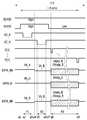
도 4는 도 1의 표시 장치 중 본 발명의 다른 일 실시 예에 따른 화소 배열 구조를 가지는 표시 패널과 보상 신호부를 구체적으로 나타낸 도면이다.4 is a diagram specifically illustrating a display panel having a pixel arrangement structure and a compensation signal unit according to another exemplary embodiment of the present invention.
특히 도 4를 참조하면 표시 장치에 포함된 표시 패널(10)은 유기 발광 다이오드(OLED)의 발광 색상에 따라 복수의 화소가 특히 펜타일(Pentile) 구조로 배열된 것을 알 수 있다. 즉, 복수의 화소는 일 방향으로 적,녹,청,녹(RGBG )의 색상으로 유기 발광 다이오드가 발광하는 기본 단위가 반복된 펜타일 구조로 배열된다.Referring to FIG. 4, it can be seen that the
도 4의 실시 예에 따른 구동 방식은 펜타일 구조로 배열된 화소 구조의 표시 패널에서 소정의 화소 영역으로 구분하여 이원적으로 보상 기간을 분리하는 방식이다.The driving method according to the embodiment of FIG. 4 is a method of dividing the compensation period into a predetermined pixel region in a display panel having a pixel structure arranged in a penta-structure, and separating the compensation period in a binary manner.
구체적으로 도 4의 실시 예에 따른 표시 패널(10)에 포함된 복수의 화소는 2개의 화소 영역인 제1 화소 영역(E)과 제2 화소 영역(O)으로 구분되고, 상기 제1 화소 영역(E)과 제2 화소 영역(O)은 각각 RGBG 펜타일 구조로 배열된 복수의 화소를 포함하는 복수의 화소 라인으로 이루어진다. 그리고 상기 제1 화소 영역(E)과 제2 화소 영역(O)은 화소 라인 단위로 서로 교차 배열된다. 설명의 편의를 위해 도 4에서 제1 화소 영역에 포함되는 복수의 화소는 E로 표기하고, 제2 화소 영역에 포함되는 복수의 화소는 O로 표기하였다. 그리고 각 화소의 유기 발광 다이오드가 빛을 방출하여 표시하는 적, 녹, 청의 색상은 각각 R, G, B로 표시하였다. 도 4의 실시 형태는 일례일 뿐이며 화소 영역의 형태는 다양하게 구성될 수 있다.Specifically, a plurality of pixels included in the
도 4의 실시 예에 따르면 표시 패널에 포함된 복수의 화소가 두 개의 화소 영역으로 구동하기 때문에 두 화소 영역에 따라 별도의 보상 제어선이 연결되고, 두 화소 영역에 포함된 복수의 화소들은 각각 상기 별도의 보상 제어선을 통해 인가되는 보상 제어 신호에 대응하여 보상 기간을 달리한다.According to the embodiment of FIG. 4, since the plurality of pixels included in the display panel are driven by two pixel regions, a separate compensation control line is connected to each of the two pixel regions, and a plurality of pixels included in the two pixel regions The compensation period is changed corresponding to the compensation control signal applied through the separate compensation control line.
도 4는 표시 패널(10)에 포함된 복수의 화소 라인 중 i번째 화소 라인부터 l번째 화소 라인 중 4개의 화소열에 해당하는 복수의 화소를 예시적으로 도시한 것이다. 4개의 화소열에 해당하는 화소들은 각각 공통적으로 대응하는 데이터 선에 연결되고 이들 데이터 선을 통해 해당 화소의 발광 색상에 대응하는 영상을 표시하는 데이터 신호를 전달받는다. 도 4에 따르면, 각 화소 라인은 화소열의 배열 방향으로 RGBG 또는 BGRG의 색상을 표시하는 화소로 배열된다.Fig. 4 exemplarily shows a plurality of pixels corresponding to four pixel columns out of the i-th pixel line to the l-th pixel line among the plurality of pixel lines included in the
그리고, 보상 신호부(50)는 표시 패널(10)과 복수의 보상 제어선으로 연결되는데, 상기 복수의 보상 제어선은 제1 보상 제어선(GCL_E)과 제2 보상 제어선(GCL_O)이다.The
제1 보상 제어선(GCL_E)은 보상 신호부(50)와 표시 패널(10)의 제1 화소 영역(E)에 포함되는 복수의 화소에 연결된다. 구체적으로 제1 보상 제어선(GCL_E)은 상기 제1 화소 영역(E)에 포함되는 복수의 화소 각각의 제4 트랜지스터(M4)의 게이트 전극에 연결되어 제1 화소 영역(E)에 포함되는 복수의 화소에 동시에 제1 보상 제어 신호(GC_E)를 전달한다.The first compensation control line GCL_E is connected to the
그리고, 제2 보상 제어선(GCL_O)은 보상 신호부(50)와 표시 패널(10)의 제2 화소 영역(O)에 포함되는 복수의 화소에 연결된다. 구체적으로 제2 보상 제어선(GCL_O)은 상기 제2 화소 영역(O)에 포함되는 복수의 화소 각각의 제4 트랜지스터(M4)의 게이트 전극에 연결되어 제2 화소 영역(O)에 포함되는 복수의 화소에 동시에 제2 보상 제어 신호(GC_O)를 전달한다.The second compensation control line GCL_O is connected to the
상기 표시 패널의 복수의 화소에 화소 영역별로 상기 제1 보상 제어 신호(GC_E)와 제2 보상 제어 신호(GC_O)가 전달되고 난 후, i번째 주사선 내지 l번째 주사선을 통해 순차적으로 대응하는 주사 신호(S[i]-S[l])이 i번째 화소 라인 내지 l번째 화소 라인의 복수의 화소에 각각 전달된다. 그러면 각 i번째 화소 라인 내지 l번째 화소 라인에 포함된 복수의 화소 각각이 순차적으로 활성화되어 각 화소열에 연결된 대응하는 데이터 선을 통해 적, 청, 녹의 색상을 표시하는 영상 데이터 신호(dataR, dataB, dataG)를 전달받아 영상을 표시한다. 도 4의 실시 예에 따른 화소의 배열 방식은 RGBG의 펜타일 방식이므로, 표시 패널에 연결된 복수의 데이터 선은 제1 화소 영역(E) 또는 제2 화소 영역(O)에 따라 적색(R)의 영상 데이터 신호(dataR) 또는 청색(B)의 영상 데이터 신호(dataB)를 전달하거나, 혹은 녹색(G)의 영상 데이터 신호(dataG)를 전달할 수 있다. 그러나 이는 일 실시 예일 뿐이며 화소의 배열 구조와 화소 영역의 다양한 실시 형태에 따라 보상 제어선의 구성과 영상 데이터 신호를 전달하는 데이터 선의 배치가 다양해질 수 있다.After the first compensation control signal GC_E and the second compensation control signal GC_O are delivered to the plurality of pixels of the display panel for each pixel region, (S [i] -S [l]) is transmitted to the plurality of pixels of the i-th pixel line to the l-th pixel line, respectively. Then, each of the plurality of pixels included in each of the i-th pixel line to the i-th pixel line is sequentially activated to sequentially output image data signals (dataR, dataB, and dataB) representing colors of red, blue, and green through corresponding data lines connected to the respective pixel lines. dataG) is received and the image is displayed. 4, the plurality of data lines connected to the display panel are arranged in the first pixel region E or the second pixel region O according to the RGBG penta scheme, It is possible to transfer the video data signal dataL or the blue video data signal dataB or the green video data signal dataG. However, this is only an embodiment, and the configuration of the compensation control line and the arrangement of the data lines for transmitting the image data signal may be varied according to the arrangement structure of the pixels and various embodiments of the pixel area.
도 5는 도 4의 실시 예에 따른 표시 패널의 일부 영역(80)에 해당하는 화소의 구체적인 회로도를 나타낸 것이다. 특히 도 4의 실시 예에 따른 표시 패널에서 k번째 화소 라인과 l번째 화소 라인에서 첫 번째 화소 열에 해당하는 상기 영역(80)은 제1 화소 영역(E)과 제2 화소 영역(O)의 두 개 화소(E_R, O_B)를 포함한다. 이들 두 개 화소(E_R, O_B)는 각각 적색의 발광 소자와 청색의 발광 소자를 가지는 화소로서 첫 번째 화소열에 연장된 대응하는 데이터 선을 통해 해당 프레임의 복수의 영상 데이터 신호 중 대응하는 적색 영상 데이터 신호(dataR) 또는 대응하는 청색 영상 데이터 신호(dataB)를 전달받는다.FIG. 5 is a specific circuit diagram of a pixel corresponding to a
도 5에 도시된 영역(80)의 회로 구조를 참조하면, 제1 화소 영역(E)에 해당하는 화소(도 5의 상위 화소)는 4개의 트랜지스터(TR1, TR2, TR3, TR4)와 2개의 커패시터(Cst1, Cst2), 및 적색으로 발광하는 유기 발광 다이오드(OLED_R)를 포함한다. 그리고, 제2 화소 영역(O)에 해당하는 화소(도 5의 하위 화소)는 4개의 트랜지스터(TR10, TR20, TR30, TR40)와 2개의 커패시터(Cst10, Cst20), 및 청색으로 발광하는 유기 발광 다이오드(OLED_B)를 포함한다. 상기 도 5에 도시된 각 화소의 구성 소자와 그 구동 동작은 상기 도 2에서 설명한 바와 동일하므로 중복되는 설명은 생략한다.Referring to the circuit structure of the
다만, 상기 제1 화소 영역(E)에 해당하는 화소의 제4 트랜지스터(TR4)의 게이트 전극으로 제1 화소 영역(E)에 대응하는 제1 보상 제어 신호(GC_E)가 전달되고, 상기 제2 화소 영역(O)에 해당하는 화소의 제4 트랜지스터(TR40)의 게이트 전극으로 제2 화소 영역(O)에 대응하는 제2 보상 제어 신호(GC_O)가 전달된다.A first compensation control signal GC_E corresponding to the first pixel region E is transferred to the gate electrode of the fourth transistor TR4 of the pixel corresponding to the first pixel region E, The second compensation control signal GC_O corresponding to the second pixel region O is transferred to the gate electrode of the fourth transistor TR40 of the pixel corresponding to the pixel region O. [
상기 제1 보상 제어 신호(GC_E)와 제2 보상 제어 신호(GC_O)는 서로 다른 기간 동안 로우 레벨의 펄스 전압으로 인가되어 제1 화소 영역과 제2 화소 영역에 각각 포함된 화소에서 바이어스 전압을 인가하는 보상 기간을 다르게 설정할 수 있다.The first compensation control signal GC_E and the second compensation control signal GC_O are applied as a low level pulse voltage for different periods to apply a bias voltage to the pixels included in the first pixel area and the second pixel area, Can be set differently.
즉, 상기 제1 보상 제어 신호(GC_E)에 대응하여 제1 화소 영역(E)에 해당하는 화소의 제4 트랜지스터(TR4)가 턴 온 되어 제3 트랜지스터(TR3)의 게이트 전극에 화이트 휘도에 대응하는 바이어스 전압을 인가함으로써 제3 트랜지스터(TR3)가 포화영역에서 구동하게 한다. 그리고 상기 제1 보상 제어 신호(GC_E)의 구동 제어 시점과 다른 시점에 전달되는 상기 제2 보상 제어 신호(GC_O)에 대응하여 제2 화소 영역(O)에 해당하는 화소의 제4 트랜지스터(TR40)가 턴 온 되고, 제3 트랜지스터(TR30)의 게이트 전극에 바이어스 전압을 인가한다.That is, the fourth transistor TR4 of the pixel corresponding to the first pixel region E is turned on corresponding to the first compensation control signal GC_E to correspond to the white luminance to the gate electrode of the third transistor TR3 The third transistor TR3 is driven in the saturation region. The fourth transistor TR40 of the pixel corresponding to the second pixel region O corresponds to the second compensation control signal GC_O transmitted at the time point different from the driving control point of the first compensation control signal GC_E. And applies a bias voltage to the gate electrode of the third transistor TR30.
서로 다른 보상 기간 동안, 제1 화소 영역(E)에 포함된 복수의 화소에 동시에 포화 영역의 구동을 위한 바이어스 전압이 인가되고, 제2 화소 영역(O)에 포함된 복수의 화소에 동시에 포화 영역의 구동을 위한 바이어스 전압이 인가된다. 그런 다음 순차로 화소 라인별로 전달되는 주사 신호(도 5에서는 S[k], S[l])에 대응하여 화소가 활성화된 뒤 대응하는 데이터 선을 통해 전달되는 해당 프레임의 영상 데이터 신호에 따른 데이터 전압을 인가받고, 그에 따른 구동 전류로 발광하여 영상을 표시하게 된다.A bias voltage for driving the saturation region is simultaneously applied to the plurality of pixels included in the first pixel region E during the different compensation period and the same voltage is applied to the plurality of pixels included in the second pixel region O at the same time, A bias voltage is applied for driving the gate electrode. Then, after the pixels are activated corresponding to the scanning signals (S [k], S [l] in FIG. 5) sequentially transmitted on the pixel line basis, data corresponding to the video data signal of the corresponding frame transmitted through the corresponding data line Receives a voltage, and emits light with a driving current corresponding thereto to display an image.
구체적으로 도 5에 도시된 화소의 구동 파형을 도 6의 타이밍도에 나타내었다.Specifically, the driving waveform of the pixel shown in Fig. 5 is shown in the timing chart of Fig.
도 6의 타이밍도에는 도 5의 영역(80)에 포함된 제1 화소 영역의 화소 및 제2 화소 영역의 화소에 전달되는 제1 전원전압(ELVDD), 제2 전원전압(ELVSS), 제1 보상 제어 신호(GC_E), 제2 보상 제어 신호(GC_O), 복수의 주사 신호(S[1]-S[n]) 중 대응하는 주사 신호(도면 미도시), 및 펜타일 화소 배열에 따라 화소열에 연장되어 각 화소에 연결된 복수의 데이터 선을 통해 전달되는 소정의 바이어스 전압이나 RGB 발광 색상에 따른 영상 데이터 신호에 따른 데이터 전압을 나타내었다. 특히 제1 화소 영역 또는 제2 화소 영역의 교차 배치에 따라 적색 화소와 청색 화소가 라인별로 반복적으로 배치된 화소열에 연결된 데이터 선을 통해 인가되는 전압을 DATA_RB로 표기하였고, 제1 화소 영역 또는 제2 화소 영역의 교차 배치임에도 불구하고 라인별로 녹색 화소가 배치된 화소열에 연결된 데이터 선을 통해 인가되는 전압을 DATA_G로 표기하였다. 그리고, 제1 화소 영역 또는 제2 화소 영역의 교차 배치에 따라 청색 화소와 적색 화소가 라인별로 반복적으로 배치된 화소열에 연결된 데이터 선을 통해 인가되는 전압을 DATA_BR로 표기하였다. 도 5의 영역(80)의 회로 구조를 참조하면 하나의 화소열에 상하로 배치된 제1 화소 영역의 화소(80-1)와 제2 화소 영역의 화소(80-2)가 각각 적색 화소와 청색 화소이므로 이들 화소에 연결된 데이터 선을 통해 인가되는 전압은 DATA_RB에 해당한다.The timing diagram of FIG. 6 shows the first power supply voltage ELVDD, the second power supply voltage ELVSS, and the first power supply voltage ELVDD transmitted to the pixels of the first pixel region and the pixels of the second pixel region included in the
이러한 도 5의 회로를 참조하여 도 6의 구동 과정을 설명하기로 한다.The driving process of FIG. 6 will be described with reference to the circuit of FIG.
먼저 a1에 제2 전원전압(ELVSS)이 하이 레벨의 전압으로 변경된다. 제2 전원전압(ELVSS)은 하이 레벨로 변경된 상태를 시점 a7까지 유지하면서 인가된다. 한편, 한 프레임 동안 제1 전원전압(ELVDD)은 소정의 하이 레벨의 전압값으로 고정되어 인가된다.First, the second power supply voltage ELVSS is changed to a high level voltage at a1. The second power supply voltage ELVSS is applied while maintaining the state changed to the high level until the time point a7. Meanwhile, the first power supply voltage ELVDD is fixed and applied at a predetermined high level during one frame.
따라서, 시점 a1 내지 시점 a7의 기간 동안 하이 레벨로 인가되는 제2 전원전압(ELVSS)에 의해 유기 발광 다이오드(OLED)의 캐소드 전극 전위가 높아져서 제2 전원전압(ELVSS) 단자 쪽으로의 전류 경로가 형성되지 않게 된다.Therefore, the cathode electrode potential of the organic light emitting diode OLED is raised by the second power supply voltage ELVSS applied at a high level during the period from the point of time a1 to the point of time a7, so that a current path toward the second power supply voltage ELVSS terminal is formed .
다음으로 시점 a2에 제1 보상 제어 신호(GC_E)가 로우 레벨의 펄스 전압으로 변화되어 시점 a3까지 로우 레벨의 펄스로 제1 화소 영역에 포함된 화소의 제4 트랜지스터(TR4)에 인가된다. 시점 a2 내지 시점 a3의 기간은 제1 보상 기간(P1)이고, 상기 제1 보상 기간(P1) 동안 로우 레벨의 제1 보상 제어 신호(GC_E)를 게이트 전극에 전달받은 제1 화소 영역의 화소(80-1)의 제4 트랜지스터(TR4)는 턴 온 되고, 대응하는 데이터 선을 통해 인가되는 전압(DATA_RB)는 소정의 바이어스 전압(Vb_R)을 인가받는다.Next, at time point a2, the first compensation control signal GC_E is changed to a low-level pulse voltage and applied to the fourth transistor TR4 of the pixel included in the first pixel region as a low-level pulse until the time point a3. The period from the point of time a2 to the point of time a3 is the first compensation period P1 and the first compensating control signal GC_E of the low level during the first compensating period P1 is supplied to the pixel of the first pixel region And the voltage (DATA_RB) applied through the corresponding data line is applied with a predetermined bias voltage Vb_R.
상기 제1 보상 기간(P1) 동안 제1 화소 영역에 포함된 화소(80-1)는 적색으로 발광하는 화소이므로 대응하는 데이터 선을 통해 적색 영상 데이터 신호의 최대 휘도(화이트 휘도)에 대응하는 상기 바이어스 전압(Vb_R)을 인가받는다.Since the pixel 80-1 included in the first pixel region during the first compensation period P1 emits red light, the pixel 80-1 corresponding to the maximum luminance (white luminance) of the red image data signal through the corresponding data line And receives the bias voltage Vb_R.
한편, 화소의 배열이 녹색 화소만으로 이루어진 화소열이거나, 화소 영역에 따라 청색 화소 및 적색 화소가 반복되도록 배열된 화소열의 경우에도 대응하는 데이터 선을 통해 상기 제1 보상 기간(P1) 동안 상기 제1 보상 제어 신호(GC_E)를 통해 소정의 바이어스 전압이 전달된다.On the other hand, in the case of a pixel column in which the arrangement of pixels is only a green pixel, or in the case of a pixel column in which blue and red pixels are arranged so as to be repeated along the pixel region, A predetermined bias voltage is transmitted through the compensation control signal GC_E.
즉, 상기 제1 보상 기간(P1) 동안 녹색 화소만으로 배치된 화소열에 연결된 데이터 선을 통해 인가되는 전압(DATA_G)은 녹색 영상 데이터 신호의 최대 화이트 휘도에 대응하는 바이어스 전압(Vb_G)이다.That is, the voltage (DATA_G) applied through the data line connected to the pixel column arranged only by the green pixel during the first compensation period (P1) is the bias voltage (Vb_G) corresponding to the maximum white luminance of the green image data signal.
그리고 동일한 기간 동안, 청색 화소 및 적색 화소가 반복되도록 배열된 화소열에 연결된 데이터 선을 통해 인가되는 전압(DATA_BR)은 청색 영상 데이터 신호의 최대 화이트 휘도에 대응하는 바이어스 전압(Vb_B)이다.During the same period, the voltage (DATA_BR) applied through the data line connected to the pixel column arranged so that the blue pixel and the red pixel are repeated is the bias voltage (Vb_B) corresponding to the maximum white luminance of the blue image data signal.
상기 제1 보상 기간(P1) 동안 제1 화소 영역(E)에 포함된 모든 화소의 제3 트랜지스터의 게이트 전극에 각 해당 화소의 발광 색상에 대응하는 화이트 휘도 전압이 바이어스 전압으로 인가됨으로써 포화 영역에서 구동할 수 있게 된다.A white luminance voltage corresponding to the emission color of each pixel is applied as a bias voltage to the gate electrode of the third transistor of all the pixels included in the first pixel region E during the first compensation period P1, .
다음으로 시점 a5에 제2 보상 제어 신호(GC_O)가 로우 레벨의 펄스 전압으로 변화되어 시점 a6까지 로우 레벨의 펄스로 제2 화소 영역에 포함된 화소의 제4 트랜지스터(TR40)에 인가된다. 시점 a5 내지 시점 a6의 기간은 제2 보상 기간(P2)이고, 상기 제2 보상 기간(P2) 동안 로우 레벨의 제2 보상 제어 신호(GC_O)를 게이트 전극에 전달받은 제2 화소 영역의 화소(80-2)의 제4 트랜지스터(TR40)는 턴 온 되고, 대응하는 데이터 선을 통해 인가되는 전압(DATA_RB)는 소정의 바이어스 전압(Vb_B)을 인가받는다.Next, at time point a5, the second compensation control signal GC_O is changed to a low-level pulse voltage and applied to the fourth transistor TR40 of the pixel included in the second pixel region as a low-level pulse until the time point a6. The period from the point of time a5 to the point of time a6 is the second compensation period P2 and the pixel of the second pixel region which receives the second compensation control signal GC_O of the low level during the second compensation period P2 to the gate electrode And the voltage (DATA_RB) applied through the corresponding data line receives a predetermined bias voltage (Vb_B).
상기 제2 보상 기간(P2) 동안 제2 화소 영역에 포함된 화소(80-2)는 청색으로 발광하는 화소이므로 대응하는 데이터 선을 통해 청색 영상 데이터 신호의 최대 휘도(화이트 휘도)에 대응하는 상기 바이어스 전압(Vb_B)을 인가받는다.Since the pixel 80-2 included in the second pixel region during the second compensation period P2 emits blue light, the pixel 80-2 corresponding to the maximum luminance (white luminance) of the blue image data signal through the corresponding data line And receives the bias voltage Vb_B.
한편, 상기 제2 보상 기간(P2) 동안 녹색 화소만으로 배치된 화소열에 연결된 데이터 선을 통해 인가되는 전압(DATA_G)은 녹색 영상 데이터 신호의 최대 화이트 휘도에 대응하는 바이어스 전압(Vb_G)이다.Meanwhile, the voltage (DATA_G) applied through the data line connected to the pixel column arranged only by the green pixel during the second compensation period (P2) is the bias voltage (Vb_G) corresponding to the maximum white luminance of the green video data signal.
그리고 동일한 기간 동안, 청색 화소 및 적색 화소가 반복되도록 배열된 화소열에 연결된 데이터 선을 통해 인가되는 전압(DATA_BR)은 적색 영상 데이터 신호의 최대 화이트 휘도에 대응하는 바이어스 전압(Vb_R)이다.During the same period, the voltage (DATA_BR) applied through the data line connected to the pixel column arranged so that the blue pixel and the red pixel are repeated is the bias voltage (Vb_R) corresponding to the maximum white luminance of the red image data signal.
따라서, 상기 제2 보상 기간(P2) 동안 제2 화소 영역(O)에 포함된 모든 화소의 제3 트랜지스터의 게이트 전극에 각 해당 화소의 발광 색상에 대응하는 화이트 휘도 전압이 바이어스 전압으로 인가됨으로써 포화 영역에서 구동할 수 있게 된다.Accordingly, during the second compensation period P2, a white luminance voltage corresponding to the emission color of each pixel is applied as a bias voltage to the gate electrode of the third transistor of all the pixels included in the second pixel region O, Area.
상기 제1 보상 기간(P1)과 제2 보상 기간(P2)이 경과하고 난 뒤, 시점 a8에 첫 번째 화소 라인에 연결된 첫 번째 주사선을 통해 첫 번째 주사 신호(S[1])가 로우 레벨의 펄스로 전달되기 시작한다. 그래서 시점 a9에 이르는 동안 화소 라인을 따라 연결된 복수의 주사선을 통해 복수의 주사 신호(S[1]-S[n])가 순차적으로 로우 레벨의 펄스로 전달된다.After the first compensating period P1 and the second compensating period P2 have elapsed, the first scanning signal S [1] through the first scanning line connected to the first pixel line at the point a8 is at a low level Begin to be transmitted as pulses. Thus, a plurality of scan signals S [1] to S [n] are successively transmitted as low-level pulses through a plurality of scan lines connected along the pixel line while reaching the point a9.
시점 a8부터 시점 a9까지 기간은 주사 기간(P3)으로서, 이 기간 동안 표시 패널(10)에 포함된 복수의 화소 중 대응하는 주사 신호를 전달받은 각 화소의 제2 트랜지스터가 순차적으로 턴 온 된다. 즉, 도 5의 회로에서 k번째 주사 신호(S[k])에 응답하여 제1 화소 영역의 화소(80-1)의 제2 트랜지스터(TR2)가 턴 온 되고, 대응하는 데이터 선을 통해 해당 프레임의 적색 영상 데이터 신호에 따른 데이터 전압(Vdata_R)을 전달받아 제2 노드(Q2)에 전달한다.The period from the point of time a8 to the point of time a9 is the scanning period P3 and the second transistor of each pixel which receives the corresponding scanning signal among the plurality of pixels included in the
제2 노드(Q2)에는 제1 트랜지스터(TR1)의 게이트 전극과 저장 커패시터(Cst2)가 연결되어 있으므로 저장 커패시터(Cst2)는 일정 기간 동안 각 프레임의 적색 영상 데이터 신호에 따른 대응하는 전압(Vdata_R)을 저장 및 유지한다. 그리고 제1 트랜지스터(TR1)는 게이트 전극에 인가되는 데이터 전압에 따른 구동 전류를 생성하여 유기 발광 다이오드(OLED_R)에 전달하여 유기 발광 다이오드(OLED_R)가 그에 따른 영상을 표시하게 한다.Since the gate electrode of the first transistor TR1 and the storage capacitor Cst2 are connected to the second node Q2, the storage capacitor Cst2 is supplied with the corresponding voltage Vdata_R corresponding to the red image data signal of each frame for a predetermined period, Lt; / RTI > The first transistor TR1 generates a driving current corresponding to a data voltage applied to the gate electrode and transmits the generated driving current to the organic light emitting diode OLED_R so that the organic light emitting diode OLED_R displays an image corresponding thereto.
한편, 순차로 전달되는 복수의 주사 신호 중에서 도 5의 회로에 도시된 바와 같이 l번째 주사 신호(S[l])가 로우 레벨로 전달되는 경우에는, 주사 신호(S[l])에 응답하여 제2 화소 영역의 화소(80-2)의 제2 트랜지스터(TR20)가 턴 온 되고, 대응하는 데이터 선을 통해 해당 프레임의 청색 영상 데이터 신호에 따른 데이터 전압(Vdata_B)을 전달받아 제2 노드(Q20)에 전달한다. 제2 노드(Q20)에는 제1 트랜지스터(TR10)의 게이트 전극과 저장 커패시터(Cst20)가 연결되어 있으므로 저장 커패시터(Cst20)는 일정 기간 동안 각 프레임의 청색 영상 데이터 신호에 따른 대응하는 전압(Vdata_B)을 저장 및 유지한다. 그리고 제1 트랜지스터(TR10)는 게이트 전극에 인가되는 데이터 전압에 따른 구동 전류를 생성하여 유기 발광 다이오드(OLED_B)에 전달하여 유기 발광 다이오드(OLED_B)가 그에 따른 영상을 표시하게 한다. 이러한 주사 기간(P3) 동안 유기 발광 다이오드의 캐소드 전극에 연결된 제2 전원전압(ELVSS)은 로우 레벨의 전압을 유지하기 때문에 유기 발광 다이오드의 캐소드 전극단 쪽으로 구동 전류 경로가 형성되어 영상을 표시할 수 있게 된다.On the other hand, in the case where the 1 < st > scan signal S [l] is transferred to the low level among the plurality of scan signals sequentially transmitted as shown in the circuit of Fig. 5, in response to the scan signal S [ The second transistor TR20 of the pixel 80-2 in the second pixel region is turned on and receives the data voltage Vdata_B according to the blue image data signal of the corresponding frame through the corresponding data line to receive the data voltage Vdata_B Q20. Since the gate electrode of the first transistor TR10 and the storage capacitor Cst20 are connected to the second node Q20, the storage capacitor Cst20 stores a corresponding voltage Vdata_B corresponding to the blue image data signal of each frame for a predetermined period of time. Lt; / RTI > The first transistor TR10 generates a driving current corresponding to a data voltage applied to the gate electrode and transmits the driving current to the organic light emitting diode OLED_B so that the organic light emitting diode OLED_B displays an image corresponding thereto. Since the second power source voltage ELVSS connected to the cathode electrode of the organic light emitting diode during the scan period P3 maintains a low level voltage, a driving current path is formed toward the cathode front end of the organic light emitting diode, .
이러한 디지털 방식으로 구동하면서 각 화소 영역을 구분하여 보상 기간을 달리 설정하고, 다르게 설정된 보상 기간을 통해 각 화소 영역별로 화소의 구동 트랜지스터에 연결된 보상 트랜지스터에 해당 발광 소자의 색상 데이터 신호의 최대 화이트 휘도 전압을 바이어스 전압으로 인가함으로써 구동 트랜지스터가 포화 영역에서 구동하게 할 수 있다. 그러면 유기 발광 다이오드의 특성 열화에 민감하게 반응하지 않을 수 있고, 영상을 표시함에 있어 휘도 편차를 줄일 수 있게 된다.The compensating transistor, which is connected to the driving transistor of the pixel in each pixel region, is supplied with the maximum white luminance voltage of the color data signal of the corresponding light emitting element The driving transistor can be driven in the saturation region. In this case, the organic light emitting diode may not be sensitive to deterioration of the characteristics of the organic light emitting diode, and luminance variations may be reduced in displaying an image.
지금까지 참조한 도면과 기재된 발명의 상세한 설명은 단지 본 발명의 예시적인 것으로서, 이는 단지 본 발명을 설명하기 위한 목적에서 사용된 것이지 의미 한정이나 특허청구범위에 기재된 본 발명의 범위를 제한하기 위하여 사용된 것은 아니다. 그러므로 본 기술 분야의 통상의 지식을 가진 자라면 이로부터 용이하게 선택하여 대체할 수 있다. 또한 당업자는 본 명세서에서 설명된 구성요소 중 일부를 성능의 열화 없이 생략하거나 성능을 개선하기 위해 구성요소를 추가할 수 있다. 뿐만 아니라, 당업자는 공정 환경이나 장비에 따라 본 명세서에서 설명한 방법 단계의 순서를 변경할 수도 있다. 따라서 본 발명의 범위는 설명된 실시형태가 아니라 특허청구범위 및 그 균등물에 의해 결정되어야 한다.It is to be understood that both the foregoing general description and the following detailed description of the present invention are illustrative and explanatory only and are intended to be illustrative of the invention and are not to be construed as limiting the scope of the invention as defined by the appended claims. It is not. Therefore, those skilled in the art can readily select and substitute it. Those skilled in the art will also appreciate that some of the components described herein can be omitted without degrading performance or adding components to improve performance. In addition, those skilled in the art may change the order of the method steps described herein depending on the process environment or equipment. Therefore, the scope of the present invention should be determined by the appended claims and equivalents thereof, not by the embodiments described.
10: 표시 패널20: 주사 구동부
30: 데이터 구동부40: 타이밍 제어부
50: 보상 신호부60: 전원 제어부
70, 80-1, 80-2: 화소10: display panel 20: scan driver
30: Data driver 40: Timing controller
50: compensation signal section 60: power source control section
70, 80-1, 80-2: pixel
Claims (22)
Translated fromKorean복수의 주사 신호를 생성하여 전달하는 주사 구동부,
상기 복수의 데이터 신호에 따른 구동 전류로 발광하는 복수의 화소를 포함하는 표시 패널,
상기 복수의 데이터 신호에 따른 데이터 전압을 복수의 화소 각각에 인가하기 이전에 상기 복수의 화소 각각에 동시에 소정의 바이어스 전압을 전달하도록 제어하는 보상 제어 신호를 생성하여 전달하는 보상 신호부,
제1 전원전압 및 제2 전원전압의 전압 레벨을 조정하여 공급하는 전원 제어부, 및
외부 영상 신호를 처리하여 상기 복수의 데이터 신호를 생성하고, 상기 데이터 구동부, 주사 구동부, 보상 신호부, 및 전원 제어부의 구동을 각각 제어하는 복수의 구동 제어 신호를 생성하는 타이밍 제어부를 포함하고,
상기 복수의 화소 각각은,
유기 발광 다이오드,
상기 제1 전원전압의 공급선에 전기적으로 연결되어 있고, 상기 유기 발광 다이오드에 구동 전류를 공급하는 제1 트랜지스터, 및
상기 제1 전원전압의 공급선과 상기 제1 트랜지스터 사이에 연결되어 상기 한 프레임 중 상기 보상 제어 신호가 전달되는 보상 기간 동안 상기 바이어스 전압을 전달받는 제3 트랜지스터를 포함하는,
표시 장치.A data driver for transmitting a plurality of data signals,
A scan driver for generating and transmitting a plurality of scan signals,
A display panel including a plurality of pixels emitting light with a driving current corresponding to the plurality of data signals,
A compensating signal unit for generating and transmitting a compensating control signal for controlling to transmit a predetermined bias voltage to each of the plurality of pixels simultaneously before applying a data voltage according to the plurality of data signals to each of the plurality of pixels,
A power supply control section for adjusting and supplying a voltage level of the first power supply voltage and the second power supply voltage;
A timing controller for generating a plurality of data signals by processing an external video signal and generating a plurality of drive control signals for controlling driving of the data driver, the scan driver, the compensation signal unit, and the power source controller,
Wherein each of the plurality of pixels comprises:
Organic light emitting diodes,
A first transistor electrically connected to a supply line of the first power supply voltage and supplying a driving current to the organic light emitting diode,
And a third transistor coupled between the supply line of the first power supply voltage and the first transistor and receiving the bias voltage during a compensation period during which the compensation control signal is transmitted in the one frame.
Display device.
상기 소정의 바이어스 전압은 상기 복수의 데이터 신호 중 최대 휘도를 표시하는 화이트 전압값으로 설정되는 표시 장치.The method according to claim 1,
Wherein the predetermined bias voltage is set to a white voltage value indicating a maximum luminance among the plurality of data signals.
상기 표시 패널은 상기 복수의 화소 중 복수의 제1 화소를 포함하는 제1 화소 영역 및 상기 복수의 제1 화소를 제외한 나머지 복수의 제2 화소를 포함하는 제2 화소 영역으로 이루어지고,
상기 보상 신호부는 상기 제1 화소 영역에 포함된 복수의 제1 화소에 연결된 제1 보상 제어선 및 상기 제2 화소 영역에 포함된 복수의 제2 화소에 연결된 제2 보상 제어선을 통해 상기 표시 패널과 연결되고,
상기 제1 보상 제어선과 상기 제2 보상 제어선 각각을 통해 상기 바이어스 전압의 인가를 제어하는 제1 보상 제어 신호 및 제2 보상 제어 신호를 각각 생성하여 전달하는 표시 장치.The method according to claim 1,
Wherein the display panel comprises a first pixel region including a plurality of first pixels among the plurality of pixels and a second pixel region including a plurality of second pixels excluding the plurality of first pixels,
Wherein the compensation signal portion includes a first compensation control line connected to a plurality of first pixels included in the first pixel region and a second compensation control line connected to a plurality of second pixels included in the second pixel region, Lt; / RTI >
And generates and transmits a first compensation control signal and a second compensation control signal for controlling the application of the bias voltage through the first compensation control line and the second compensation control line, respectively.
상기 제1 화소 영역에 포함된 복수의 제1 화소와 상기 제2 화소 영역에 포함된 복수의 제2 화소는 제1 색상 화소, 제2 색상 화소, 제3 색상 화소, 및 상기 제2 색상 화소의 단위로 반복적으로 구성되는 표시 장치.The method of claim 3,
Wherein a plurality of first pixels included in the first pixel region and a plurality of second pixels included in the second pixel region are disposed in a first color pixel, a second color pixel, a third color pixel, and a second color pixel, Wherein the display unit is repeatedly constituted by a plurality of units.
상기 보상 신호부는 상기 표시 패널에 포함된 복수의 화소에 복수의 데이터 신호를 전달하기 이전에 상기 제1 보상 제어 신호 및 상기 제2 보상 제어 신호를 전달하는 것을 특징으로 하는 표시 장치.The method of claim 3,
Wherein the compensation signal unit transfers the first compensation control signal and the second compensation control signal before transmitting a plurality of data signals to a plurality of pixels included in the display panel.
상기 바이어스 전압은 상기 데이터 구동부와 상기 복수의 화소 각각에 연결된 복수의 데이터 선을 통해 상기 복수의 화소 각각에 인가되는 것을 특징으로 하는 표시 장치.The method according to claim 1,
Wherein the bias voltage is applied to each of the plurality of pixels through a plurality of data lines connected to the data driver and each of the plurality of pixels.
상기 복수의 화소 각각은 보상 제어 신호에 따라 스위칭 동작이 제어되는 스위칭 소자를 포함하고, 상기 바이어스 전압은 상기 보상 제어 신호에 대응하여 턴 온 된 스위칭 소자를 통해 인가되는 것을 특징으로 하는 표시 장치.The method according to claim 6,
Wherein each of the plurality of pixels includes a switching element whose switching operation is controlled in accordance with a compensation control signal, and the bias voltage is applied through a switching element turned on corresponding to the compensation control signal.
상기 복수의 화소 각각은 상기 보상 제어 신호에 대응하여 상기 바이어스 전압을 복수의 화소 각각의 구동 트랜지스터의 소스 전극에 인가받는 것을 특징으로 하는 표시 장치.The method according to claim 1,
Wherein each of the plurality of pixels receives the bias voltage corresponding to the compensation control signal to the source electrode of the driving transistor of each of the plurality of pixels.
상기 전원 제어부는 한 프레임 동안 상기 제1 전원전압을 소정의 하이 레벨 전압으로 공급하고, 상기 한 프레임 중 상기 보상 제어 신호가 전달되는 보상 기간 동안 상기 제2 전원전압을 소정의 하이 레벨 전압으로 공급하는 것을 특징으로 하는 표시 장치.The method according to claim 1,
The power supply controller supplies the first power supply voltage at a predetermined high level voltage for one frame and supplies the second power supply voltage at a predetermined high level voltage during a compensation period during which the compensation control signal is transmitted in one frame And the display device.
상기 복수의 화소 각각은,
상기 복수의 데이터 신호를 전달하는 복수의 데이터 선 중 대응하는 데이터 선에 연결되어 한 프레임의 복수의 데이터 신호에 따른 데이터 전압을 상기 제2 트랜지스터의 게이트 전극에 전달하는 제2 트랜지스터,
상기 대응하는 데이터 선에 연결되어 상기 한 프레임 중 상기 보상 기간 동안 상기 보상 제어 신호에 대응하여 상기 데이터 선을 통해 바이어스 전압을 상기 제3 트랜지스터의 게이트 전극에 전달하는 제4 트랜지스터,
상기 제3 트랜지스터의 게이트 전극에 연결되어 있는 제1 커패시터, 및
상기 제1 트랜지스터의 게이트 전극에 연결되어 있는 제2 커패시터를 더 포함하는 표시 장치.The method according to claim 1,
Wherein each of the plurality of pixels comprises:
A second transistor coupled to a corresponding one of the plurality of data lines for transmitting the plurality of data signals and transmitting a data voltage corresponding to the plurality of data signals of one frame to the gate electrode of the second transistor,
A fourth transistor coupled to the corresponding data line for transmitting a bias voltage to the gate electrode of the third transistor through the data line corresponding to the compensation control signal during the compensation period of the one frame,
A first capacitor coupled to the gate electrode of the third transistor,
And a second capacitor connected to the gate electrode of the first transistor.
상기 복수의 화소 각각은 제1 화소 영역에 포함되는 복수의 제1 화소와 제2 화소 영역에 포함되는 복수의 제2 화소를 포함하고,
상기 복수의 제1 화소의 상기 제4 트랜지스터의 게이트 전극은 상기 보상 기간 중 제1 보상 기간 동안 제1 보상 제어 신호를 인가받고,
상기 복수의 제2 화소의 상기 제4 트랜지스터의 게이트 전극은 상기 보상 기간 중 상기 제1 보상 기간 이후의 제2 보상 기간 동안 제2 보상 제어 신호를 인가받는 것을 특징으로 하는 표시 장치.11. The method of claim 10,
Wherein each of the plurality of pixels includes a plurality of first pixels included in the first pixel region and a plurality of second pixels included in the second pixel region,
A gate electrode of the fourth transistor of the plurality of first pixels is supplied with a first compensation control signal during a first compensation period during the compensation period,
And a gate electrode of the fourth transistor of the plurality of second pixels receives a second compensation control signal during a second compensation period after the first compensation period during the compensation period.
Priority Applications (2)
| Application Number | Priority Date | Filing Date | Title |
|---|---|---|---|
| KR1020120137231AKR101987424B1 (en) | 2012-11-29 | 2012-11-29 | Pixel, diplay device comprising the pixel and driving method of the diplay device |
| US13/901,064US9159263B2 (en) | 2012-11-29 | 2013-05-23 | Pixel with enhanced luminance non-uniformity, a display device comprising the pixel and driving method of the display device |
Applications Claiming Priority (1)
| Application Number | Priority Date | Filing Date | Title |
|---|---|---|---|
| KR1020120137231AKR101987424B1 (en) | 2012-11-29 | 2012-11-29 | Pixel, diplay device comprising the pixel and driving method of the diplay device |
Publications (2)
| Publication Number | Publication Date |
|---|---|
| KR20140069671A KR20140069671A (en) | 2014-06-10 |
| KR101987424B1true KR101987424B1 (en) | 2019-06-11 |
Family
ID=50772868
Family Applications (1)
| Application Number | Title | Priority Date | Filing Date |
|---|---|---|---|
| KR1020120137231AActiveKR101987424B1 (en) | 2012-11-29 | 2012-11-29 | Pixel, diplay device comprising the pixel and driving method of the diplay device |
Country Status (2)
| Country | Link |
|---|---|
| US (1) | US9159263B2 (en) |
| KR (1) | KR101987424B1 (en) |
Families Citing this family (14)
| Publication number | Priority date | Publication date | Assignee | Title |
|---|---|---|---|---|
| KR20140133189A (en)* | 2013-05-10 | 2014-11-19 | 삼성디스플레이 주식회사 | Pixel of an organic light emitting display device and organic light emitting display device |
| KR102234523B1 (en)* | 2014-05-29 | 2021-04-01 | 삼성디스플레이 주식회사 | Pixel circuit and organic light emitting display device including the same |
| KR102230928B1 (en)* | 2014-10-13 | 2021-03-24 | 삼성디스플레이 주식회사 | Orgainic light emitting display and driving method for the same |
| CN105023539B (en)* | 2015-07-10 | 2017-11-28 | 北京大学深圳研究生院 | Offset peripheral system, method and the display system of a kind of picture element matrix |
| KR102406605B1 (en)* | 2015-08-27 | 2022-06-09 | 삼성디스플레이 주식회사 | Organic light emitting display device |
| KR102456297B1 (en) | 2016-04-15 | 2022-10-20 | 삼성디스플레이 주식회사 | Pixel circuit and method of driving the same |
| KR102795189B1 (en)* | 2016-10-05 | 2025-04-11 | 삼성디스플레이 주식회사 | Head mounted display device |
| KR102394683B1 (en)* | 2018-03-06 | 2022-05-09 | 삼성디스플레이 주식회사 | Display panel of organic light emitting diode display device having a pentile pixel structure |
| CN108427546B (en)* | 2018-05-03 | 2022-03-08 | 深圳Tcl新技术有限公司 | Full screen adaptation method of display device, display device and storage medium |
| KR102820515B1 (en)* | 2019-10-10 | 2025-06-17 | 삼성디스플레이 주식회사 | Display device |
| CN111210767A (en) | 2020-03-05 | 2020-05-29 | 深圳市华星光电半导体显示技术有限公司 | Pixel driving circuit, driving method thereof and display panel |
| CN111508416B (en)* | 2020-04-30 | 2021-09-03 | 武汉华星光电半导体显示技术有限公司 | Display and driving method thereof |
| KR20230124160A (en)* | 2022-02-17 | 2023-08-25 | 삼성디스플레이 주식회사 | Pixel and display device |
| US20250261446A1 (en)* | 2024-02-08 | 2025-08-14 | Wuhan China Star Optoelectronics Semiconductor Display Technology Co., Ltd. | Display panel and display device |
Citations (1)
| Publication number | Priority date | Publication date | Assignee | Title |
|---|---|---|---|---|
| KR100833753B1 (en)* | 2006-12-21 | 2008-05-30 | 삼성에스디아이 주식회사 | Organic electroluminescent display and driving method thereof |
Family Cites Families (8)
| Publication number | Priority date | Publication date | Assignee | Title |
|---|---|---|---|---|
| KR100517664B1 (en) | 2002-08-30 | 2005-09-28 | 인더스트리얼 테크놀로지 리써치 인스티튜트 | Active matrix led pixel driving circuit |
| US7830352B2 (en)* | 2005-01-14 | 2010-11-09 | Au Optronics Corp. | Driving circuit for flat panel display which provides a horizontal start signal to first and second shift register cells |
| JP4356616B2 (en)* | 2005-01-20 | 2009-11-04 | セイコーエプソン株式会社 | Power supply circuit, display driver, electro-optical device, electronic apparatus, and control method for power supply circuit |
| JP4552844B2 (en)* | 2005-06-09 | 2010-09-29 | セイコーエプソン株式会社 | LIGHT EMITTING DEVICE, ITS DRIVE METHOD, AND ELECTRONIC DEVICE |
| JP4207988B2 (en) | 2006-07-03 | 2009-01-14 | セイコーエプソン株式会社 | Light emitting device, pixel circuit driving method and driving circuit |
| KR101458911B1 (en) | 2008-05-07 | 2014-11-12 | 삼성디스플레이 주식회사 | Display device |
| KR101860860B1 (en)* | 2011-03-16 | 2018-07-02 | 삼성디스플레이 주식회사 | Organic Light Emitting Display and Driving Method Thereof |
| KR101893167B1 (en)* | 2012-03-23 | 2018-10-05 | 삼성디스플레이 주식회사 | Pixel circuit, method of driving the same, and method of driving a pixel circuit |
- 2012
- 2012-11-29KRKR1020120137231Apatent/KR101987424B1/enactiveActive
- 2013
- 2013-05-23USUS13/901,064patent/US9159263B2/enactiveActive
Patent Citations (1)
| Publication number | Priority date | Publication date | Assignee | Title |
|---|---|---|---|---|
| KR100833753B1 (en)* | 2006-12-21 | 2008-05-30 | 삼성에스디아이 주식회사 | Organic electroluminescent display and driving method thereof |
Also Published As
| Publication number | Publication date |
|---|---|
| US9159263B2 (en) | 2015-10-13 |
| KR20140069671A (en) | 2014-06-10 |
| US20140146028A1 (en) | 2014-05-29 |
Similar Documents
| Publication | Publication Date | Title |
|---|---|---|
| KR101987424B1 (en) | Pixel, diplay device comprising the pixel and driving method of the diplay device | |
| KR101082234B1 (en) | Organic light emitting display device and driving method thereof | |
| KR102141238B1 (en) | Pixel and Organic Light Emitting Display Device | |
| US9153162B2 (en) | Pixel, display device comprising the pixel and driving method of the display device | |
| US9570009B2 (en) | Pixel circuit of display device, organic light emitting display device and method for driving the same | |
| US9135887B2 (en) | Display device and driving method of the same | |
| KR101040893B1 (en) | Pixel and organic light emitting display device using same | |
| US9215777B2 (en) | Pixel and organic light emitting display device using the same | |
| KR101073281B1 (en) | Organic light emitting display device and driving method thereof | |
| KR102363339B1 (en) | Organic light emitting display and driving method of the same | |
| US11482174B2 (en) | Display device and driving method of the display device | |
| KR101738920B1 (en) | Organic Light Emitting Display Device | |
| KR101975489B1 (en) | Display device and driving method thereof | |
| KR102137521B1 (en) | Pixel circuit and driving method thereof | |
| US9318052B2 (en) | Compensating organic light emitting diode display device and method for driving the same using two adjacent gate lines per pixel | |
| US9275581B2 (en) | Pixel, display device comprising the same and driving method thereof | |
| US9870734B2 (en) | Organic light emitting display and driving method thereof | |
| KR101964768B1 (en) | Pixel, display device comprising the same and driving method thereof | |
| JP2016081030A (en) | Organic light emitting display | |
| TW201621863A (en) | Organic light emitting display | |
| KR102206602B1 (en) | Pixel and organic light emitting display device using the same | |
| KR20200091062A (en) | Display device and driving method thereof | |
| KR20120009669A (en) | Pixel and organic light emitting display device using same | |
| KR20160052877A (en) | Organic light emitting display device and method of driving the same | |
| KR20140053605A (en) | Pixel, display device comprising the same and driving method thereof |
Legal Events
| Date | Code | Title | Description |
|---|---|---|---|
| PA0109 | Patent application | Patent event code:PA01091R01D Comment text:Patent Application Patent event date:20121129 | |
| PG1501 | Laying open of application | ||
| A201 | Request for examination | ||
| PA0201 | Request for examination | Patent event code:PA02012R01D Patent event date:20171023 Comment text:Request for Examination of Application Patent event code:PA02011R01I Patent event date:20121129 Comment text:Patent Application | |
| E902 | Notification of reason for refusal | ||
| PE0902 | Notice of grounds for rejection | Comment text:Notification of reason for refusal Patent event date:20180917 Patent event code:PE09021S01D | |
| E701 | Decision to grant or registration of patent right | ||
| PE0701 | Decision of registration | Patent event code:PE07011S01D Comment text:Decision to Grant Registration Patent event date:20190306 | |
| GRNT | Written decision to grant | ||
| PR0701 | Registration of establishment | Comment text:Registration of Establishment Patent event date:20190603 Patent event code:PR07011E01D | |
| PR1002 | Payment of registration fee | Payment date:20190603 End annual number:3 Start annual number:1 | |
| PG1601 | Publication of registration | ||
| PR1001 | Payment of annual fee | Payment date:20220523 Start annual number:4 End annual number:4 | |
| PR1001 | Payment of annual fee | Payment date:20230524 Start annual number:5 End annual number:5 | |
| PR1001 | Payment of annual fee | Payment date:20240523 Start annual number:6 End annual number:6 |