KR101987191B1 - Liquid crystal display device and method for driving the same - Google Patents
Liquid crystal display device and method for driving the sameDownload PDFInfo
- Publication number
- KR101987191B1 KR101987191B1KR1020120096229AKR20120096229AKR101987191B1KR 101987191 B1KR101987191 B1KR 101987191B1KR 1020120096229 AKR1020120096229 AKR 1020120096229AKR 20120096229 AKR20120096229 AKR 20120096229AKR 101987191 B1KR101987191 B1KR 101987191B1
- Authority
- KR
- South Korea
- Prior art keywords
- tmic
- data
- liquid crystal
- timing controller
- interface
- Prior art date
- Legal status (The legal status is an assumption and is not a legal conclusion. Google has not performed a legal analysis and makes no representation as to the accuracy of the status listed.)
- Active
Links
Images


Classifications
- G—PHYSICS
- G02—OPTICS
- G02F—OPTICAL DEVICES OR ARRANGEMENTS FOR THE CONTROL OF LIGHT BY MODIFICATION OF THE OPTICAL PROPERTIES OF THE MEDIA OF THE ELEMENTS INVOLVED THEREIN; NON-LINEAR OPTICS; FREQUENCY-CHANGING OF LIGHT; OPTICAL LOGIC ELEMENTS; OPTICAL ANALOGUE/DIGITAL CONVERTERS
- G02F1/00—Devices or arrangements for the control of the intensity, colour, phase, polarisation or direction of light arriving from an independent light source, e.g. switching, gating or modulating; Non-linear optics
- G02F1/01—Devices or arrangements for the control of the intensity, colour, phase, polarisation or direction of light arriving from an independent light source, e.g. switching, gating or modulating; Non-linear optics for the control of the intensity, phase, polarisation or colour
- G02F1/13—Devices or arrangements for the control of the intensity, colour, phase, polarisation or direction of light arriving from an independent light source, e.g. switching, gating or modulating; Non-linear optics for the control of the intensity, phase, polarisation or colour based on liquid crystals, e.g. single liquid crystal display cells
- G02F1/133—Constructional arrangements; Operation of liquid crystal cells; Circuit arrangements
- G—PHYSICS
- G09—EDUCATION; CRYPTOGRAPHY; DISPLAY; ADVERTISING; SEALS
- G09G—ARRANGEMENTS OR CIRCUITS FOR CONTROL OF INDICATING DEVICES USING STATIC MEANS TO PRESENT VARIABLE INFORMATION
- G09G3/00—Control arrangements or circuits, of interest only in connection with visual indicators other than cathode-ray tubes
- G09G3/20—Control arrangements or circuits, of interest only in connection with visual indicators other than cathode-ray tubes for presentation of an assembly of a number of characters, e.g. a page, by composing the assembly by combination of individual elements arranged in a matrix no fixed position being assigned to or needed to be assigned to the individual characters or partial characters
- G09G3/34—Control arrangements or circuits, of interest only in connection with visual indicators other than cathode-ray tubes for presentation of an assembly of a number of characters, e.g. a page, by composing the assembly by combination of individual elements arranged in a matrix no fixed position being assigned to or needed to be assigned to the individual characters or partial characters by control of light from an independent source
- G09G3/36—Control arrangements or circuits, of interest only in connection with visual indicators other than cathode-ray tubes for presentation of an assembly of a number of characters, e.g. a page, by composing the assembly by combination of individual elements arranged in a matrix no fixed position being assigned to or needed to be assigned to the individual characters or partial characters by control of light from an independent source using liquid crystals
- G09G3/3611—Control of matrices with row and column drivers
- G—PHYSICS
- G02—OPTICS
- G02F—OPTICAL DEVICES OR ARRANGEMENTS FOR THE CONTROL OF LIGHT BY MODIFICATION OF THE OPTICAL PROPERTIES OF THE MEDIA OF THE ELEMENTS INVOLVED THEREIN; NON-LINEAR OPTICS; FREQUENCY-CHANGING OF LIGHT; OPTICAL LOGIC ELEMENTS; OPTICAL ANALOGUE/DIGITAL CONVERTERS
- G02F1/00—Devices or arrangements for the control of the intensity, colour, phase, polarisation or direction of light arriving from an independent light source, e.g. switching, gating or modulating; Non-linear optics
- G02F1/01—Devices or arrangements for the control of the intensity, colour, phase, polarisation or direction of light arriving from an independent light source, e.g. switching, gating or modulating; Non-linear optics for the control of the intensity, phase, polarisation or colour
- G02F1/13—Devices or arrangements for the control of the intensity, colour, phase, polarisation or direction of light arriving from an independent light source, e.g. switching, gating or modulating; Non-linear optics for the control of the intensity, phase, polarisation or colour based on liquid crystals, e.g. single liquid crystal display cells
- G02F1/133—Constructional arrangements; Operation of liquid crystal cells; Circuit arrangements
- G02F1/1333—Constructional arrangements; Manufacturing methods
- G02F1/1345—Conductors connecting electrodes to cell terminals
- G—PHYSICS
- G09—EDUCATION; CRYPTOGRAPHY; DISPLAY; ADVERTISING; SEALS
- G09G—ARRANGEMENTS OR CIRCUITS FOR CONTROL OF INDICATING DEVICES USING STATIC MEANS TO PRESENT VARIABLE INFORMATION
- G09G3/00—Control arrangements or circuits, of interest only in connection with visual indicators other than cathode-ray tubes
- G09G3/20—Control arrangements or circuits, of interest only in connection with visual indicators other than cathode-ray tubes for presentation of an assembly of a number of characters, e.g. a page, by composing the assembly by combination of individual elements arranged in a matrix no fixed position being assigned to or needed to be assigned to the individual characters or partial characters
- G09G3/2092—Details of a display terminals using a flat panel, the details relating to the control arrangement of the display terminal and to the interfaces thereto
- G—PHYSICS
- G09—EDUCATION; CRYPTOGRAPHY; DISPLAY; ADVERTISING; SEALS
- G09G—ARRANGEMENTS OR CIRCUITS FOR CONTROL OF INDICATING DEVICES USING STATIC MEANS TO PRESENT VARIABLE INFORMATION
- G09G3/00—Control arrangements or circuits, of interest only in connection with visual indicators other than cathode-ray tubes
- G09G3/20—Control arrangements or circuits, of interest only in connection with visual indicators other than cathode-ray tubes for presentation of an assembly of a number of characters, e.g. a page, by composing the assembly by combination of individual elements arranged in a matrix no fixed position being assigned to or needed to be assigned to the individual characters or partial characters
- G09G3/34—Control arrangements or circuits, of interest only in connection with visual indicators other than cathode-ray tubes for presentation of an assembly of a number of characters, e.g. a page, by composing the assembly by combination of individual elements arranged in a matrix no fixed position being assigned to or needed to be assigned to the individual characters or partial characters by control of light from an independent source
- G09G3/36—Control arrangements or circuits, of interest only in connection with visual indicators other than cathode-ray tubes for presentation of an assembly of a number of characters, e.g. a page, by composing the assembly by combination of individual elements arranged in a matrix no fixed position being assigned to or needed to be assigned to the individual characters or partial characters by control of light from an independent source using liquid crystals
- G09G3/3611—Control of matrices with row and column drivers
- G09G3/3696—Generation of voltages supplied to electrode drivers
- G—PHYSICS
- G09—EDUCATION; CRYPTOGRAPHY; DISPLAY; ADVERTISING; SEALS
- G09G—ARRANGEMENTS OR CIRCUITS FOR CONTROL OF INDICATING DEVICES USING STATIC MEANS TO PRESENT VARIABLE INFORMATION
- G09G2370/00—Aspects of data communication
- G09G2370/08—Details of image data interface between the display device controller and the data line driver circuit
- G—PHYSICS
- G09—EDUCATION; CRYPTOGRAPHY; DISPLAY; ADVERTISING; SEALS
- G09G—ARRANGEMENTS OR CIRCUITS FOR CONTROL OF INDICATING DEVICES USING STATIC MEANS TO PRESENT VARIABLE INFORMATION
- G09G2370/00—Aspects of data communication
- G09G2370/14—Use of low voltage differential signaling [LVDS] for display data communication
- G—PHYSICS
- G09—EDUCATION; CRYPTOGRAPHY; DISPLAY; ADVERTISING; SEALS
- G09G—ARRANGEMENTS OR CIRCUITS FOR CONTROL OF INDICATING DEVICES USING STATIC MEANS TO PRESENT VARIABLE INFORMATION
- G09G3/00—Control arrangements or circuits, of interest only in connection with visual indicators other than cathode-ray tubes
- G09G3/20—Control arrangements or circuits, of interest only in connection with visual indicators other than cathode-ray tubes for presentation of an assembly of a number of characters, e.g. a page, by composing the assembly by combination of individual elements arranged in a matrix no fixed position being assigned to or needed to be assigned to the individual characters or partial characters
- G09G3/34—Control arrangements or circuits, of interest only in connection with visual indicators other than cathode-ray tubes for presentation of an assembly of a number of characters, e.g. a page, by composing the assembly by combination of individual elements arranged in a matrix no fixed position being assigned to or needed to be assigned to the individual characters or partial characters by control of light from an independent source
- G09G3/36—Control arrangements or circuits, of interest only in connection with visual indicators other than cathode-ray tubes for presentation of an assembly of a number of characters, e.g. a page, by composing the assembly by combination of individual elements arranged in a matrix no fixed position being assigned to or needed to be assigned to the individual characters or partial characters by control of light from an independent source using liquid crystals
- G09G3/3611—Control of matrices with row and column drivers
- G09G3/3685—Details of drivers for data electrodes
- G09G3/3688—Details of drivers for data electrodes suitable for active matrices only
Landscapes
- Physics & Mathematics (AREA)
- Engineering & Computer Science (AREA)
- General Physics & Mathematics (AREA)
- Theoretical Computer Science (AREA)
- Computer Hardware Design (AREA)
- Crystallography & Structural Chemistry (AREA)
- Chemical & Material Sciences (AREA)
- Nonlinear Science (AREA)
- Mathematical Physics (AREA)
- Optics & Photonics (AREA)
- Control Of Indicators Other Than Cathode Ray Tubes (AREA)
- Liquid Crystal Display Device Control (AREA)
- Liquid Crystal (AREA)
Abstract
Translated fromKoreanDescription
Translated fromKorean본 발명은 액정 디스플레이 장치에 관한 것으로, 특히 TMIC(Timing controller merged IC)을 적용함과 아울러, 인쇄회로보드(PCB)의 라인 수를 줄여 제조비용을 절감시키고, 노이즈의 영향을 줄일 수 있는 액정 디스플레이 장치와 이의 구동방법에 관한 것이다.BACKGROUND OF THE
액정 디스플레이 장치(liquid crystal display device)는 양산 기술의 발전, 구동수단의 용이성, 저전력 소비, 고화질 구현 및 대화면 구현의 장점으로 대중화되었다. 액정 디스플레이 장치는 노트북 PC와 같은 휴대용 컴퓨터, 사무 자동화 기기, 휴대용 멀티 미디어 기기, 옥내/옥외 광고 디스플레이 장치 등 여러 분야에 적용되고 있으며, 적용 분야가 지속적으로 확대되고 있다.Liquid crystal display devices have become popular due to the development of mass production technology, ease of driving means, low power consumption, high definition and large screen. Liquid crystal display devices are applied to various fields such as portable computers such as notebook PCs, office automation devices, portable multimedia devices, indoor / outdoor advertising display devices, and the field of application is continuously expanding.
도 1은 종래 기술에 따른 액정 디스플레이 장치를 개략적으로 나타내는 도면이고, 도 2는 종래 기술에 따른 인쇄회로보드에 실장된 복수의 TMIC 및 커넥터의 접속 구조를 나타내는 도면이다.1 is a view schematically showing a liquid crystal display device according to the prior art, and FIG. 2 is a view showing a connection structure of a plurality of TMICs and connectors mounted on a printed circuit board according to the prior art.
도 1 및 도 2를 참조하면, 종래 기술에 따른 액정 디스플레이 장치는 화상을 표시하는 액정 패널(10), 액정 패널(10)에 광을 공급하는 백라이트 유닛(미도시) 및 액정 패널(10)을 구동시키기 위한 구동 회로부를 포함한다.1 and 2, a liquid crystal display device according to the related art includes a
액정 패널(10)은 상부 기판(컬러필터 어레이 기판), 하부 기판(TFT 어레이 기판) 및 상부 기판과 하부 기판 사이에 개재된 액정층을 포함한다. 이러한, 액정 패널(10)은 픽셀들(pixels)이 매트릭스 형태로 배열되며, 백라이트 유닛에서 조사되는 광의 투과율을 조절하여 화상을 표시한다.The
구동 회로부는 게이트 드라이버(15), 복수의 TMIC(30, (timing controller merged IC)및 전원 공급부(40, PMIC)를 포함한다. 여기서, 복수의 TMIC(30)와 전원 공급부(40)는 인쇄회로보드(20, Printed Circuit Board, 이하 'PCB'라 함)에 실장된다.The driving circuit unit includes a
PCB(20)에는 외부로부터 입력된 신호를 복수의 TMIC(30)로 전송하기 위한 커넥터(50) 및 다수의 라인(60)이 형성되어 있다. 또한, PCB(20)에는 TMIC(30)의 구동 및 감마전압의 생성을 위한 컨트롤 데이터가 저장된 EEPROM(70)이 형성되어 있다.The
게이트 드라이버(15)는 GIP(gate in panel) 방식으로 액정 패널(10)의 비표시 영역에 형성되어 있으며, 액정 패널(10)에 형성된 복수의 게이트 라인에 스캔 신호를 순차적으로 공급한다.The
영상 신호 및 제어 신호(타이밍 신호를 포함)는 LVDS(low voltage differential signal)로 커넥터(50)에 입력되고, 커넥터(50)에 접속된 복수의 라인(60)을 통해 LVDS가 복수의 TMIC(30)에 공급된다. 이때, 커넥터(50)로 입력된 LVDS를 멀티 드랍(multi drop) 방식으로 복수의 TMIC(30)에 공급한다.The video signal and the control signal (including the timing signal) are input to the
복수의 TMIC(30)는 타이밍 컨트롤러와 데이터 드라이버를 포함하여 구성되며, 게이트 드라이버(15) 및 데이터 드라이버의 제어를 위한 제어 신호를 생성하여 게이트 드라이버 및 데이터 드라이버에 공급한다. 또한, TMIC(30)에 구성된 데이터 드라이버는 입력된 LVDS에 포함된 영상 신호에 따라 아날로그 데이터 전압을 생성하여 액정 패널(10)에 형성된 복수의 데이터 라인에 공급한다.The plurality of
상술한 구성을 포함하는 종래 기술에 따른 액정 디스플레이 장치는 액정 패널(10)의 픽셀들에 데이터 전압을 공급하기 위해서 복수의 TMIC(30)가 적용됨으로 인해 제조 비용이 증가되는 문제점이 있다.The liquid crystal display device according to the related art including the above-described configuration has a problem in that manufacturing cost is increased because a plurality of
액정 패널(10)이 15.6인치의 화면 크기를 가지는 경우에 일반적으로 3개의 TMIC(30)가 적용되는데, 하나의 LCM(liquid crystal module)에 3개의 TMIC(30)가 적용되어 가격 경쟁력이 낮아지는 문제점이 있다.When the
또한, 복수의 TMIC(30)에 LVDS를 공급하기 위해서, PCB(20)에 다수의 라인(60)이 형성됨으로 인해 PCB(20)의 면적이 증가되는 문제점이 있다. 최근에 들어, 액정 디스플레이 장치의 구동 회로부가 실장되는 PCB(20)의 면적을 축소시키려 하고 있으나, 복수의 라인(60)을 형성함으로 인해 PCB(20) 면적을 축소하는데 한계가 있다.In addition, in order to supply LVDS to the plurality of
또한, PCB(20)에 3개의 TMIC(30)가 실장되는 경우, 3개의 TMIC(30) 각각에 LVDS를 전송하기 위해 다수의 라인(60)이 PCB(20)에 형성되어야 한다. 작은 면적 안에 다수의 라인을 형성하기 위해서 고가의 Build-up PCB가 적용되어 액정 디스플레이 장치의 제조비용이 증가하는 문제점 있다.In addition, when three
본 발명은 상술한 문제점을 해결하기 위한 것으로서, 복수의 TMIC가 적용되어 증가된 제조비용을 절감시킬 수 있는 액정 디스플레이 장치와 이의 구동방법을 제공하는 것을 기술적 과제로 한다.Disclosure of Invention The present invention has been made in view of the above-described problems, and it is a technical object of the present invention to provide a liquid crystal display device and a driving method thereof capable of reducing an increased manufacturing cost by applying a plurality of TMIC.
본 발명은 상술한 문제점을 해결하기 위한 것으로서, 구동 회로부가 실장되는 고가의 build-up PCB를 저가의 MLB(multi layer board) PCB 로 변경하여 제조비용을 절감시킬 수 있는 액정 디스플레이 장치를 제공하는 것을 기술적 과제로 한다.The present invention is to solve the above problems, to provide a liquid crystal display device that can reduce the manufacturing cost by changing the expensive build-up PCB on which the drive circuit is mounted to a low-cost multi-layer board (MLB) PCB It is a technical problem.
본 발명은 상술한 문제점을 해결하기 위한 것으로서, 구동 회로부가 실장되는 PCB의 면적을 감소시킬 수 있는 액정 디스플레이 장치를 제공하는 것을 기술적 과제로 한다.SUMMARY OF THE INVENTION The present invention has been made in view of the above-described problems, and it is an object of the present invention to provide a liquid crystal display device capable of reducing the area of a PCB on which a driving circuit unit is mounted.
본 발명은 상술한 문제점을 해결하기 위한 것으로서, PCB에 실장된 TMIC에 LVDS를 공급하기 위한 라인을 수를 감소시킬 수 있는 액정 디스플레이 장치를 제공하는 것을 기술적 과제로 한다.SUMMARY OF THE INVENTION The present invention has been made in view of the above-described problems, and it is a technical problem to provide a liquid crystal display device capable of reducing the number of lines for supplying LVDS to a TMIC mounted on a PCB.
본 발명은 상술한 문제점을 해결하기 위한 것으로서, 감마전압 생성부를 데이터 드라이버에 실장하여 제조 비용을 절감시킬 수 있는 액정 디스플레이 장치와 이의 구동방법을 제공하는 것을 기술적 과제로 한다.SUMMARY OF THE INVENTION The present invention has been made in an effort to provide a liquid crystal display device and a driving method thereof capable of reducing manufacturing costs by mounting a gamma voltage generator in a data driver.
위에서 언급된 본 발명의 기술적 과제 외에도, 본 발명의 다른 특징 및 이점들이 이하에서 기술되거나, 그러한 기술 및 설명으로부터 본 발명이 속하는 기술분야에서 통상의 지식을 가진 자에게 명확하게 이해될 수 있을 것이다.In addition to the technical task of the present invention mentioned above, other features and advantages of the present invention will be described below, or from such description and description will be clearly understood by those skilled in the art.
본 발명의 실시 예에 따른 액정 디스플레이 장치는 액정 패널; 상기 액정 패널의 비표시 영역에 형성된 게이트 드라이버; 및 타이밍 컨트롤러와 데이터 드라이버가 결합된 TMIC(timing controller merged IC)와, 상기 TMIC에서 공급된 패킷 데이터에 의해 구동되는 복수의 데이터 드라이버와, 전원 공급부를 실장하는 인쇄회로보드를 포함한다.Liquid crystal display device according to an embodiment of the present invention is a liquid crystal panel; A gate driver formed in the non-display area of the liquid crystal panel; And a timing controller merged IC (TMIC) in which a timing controller and a data driver are combined, a plurality of data drivers driven by packet data supplied from the TMIC, and a printed circuit board on which a power supply unit is mounted.
본 발명의 실시 예에 따른 액정 디스플레이 장치의 구동방법은 인쇄회로보드에 하나의 TMIC 및 복수의 데이터 드라이버가 실장된 액정 디스플레이 장치의 구동방법에 있어서, 영상 신호 및 제어 신호가 포함된 LVDS(low voltage differential signal)가 상기 TMIC에 입력되는 단계; 상기 TMIC에 구성된 데이터 드라이버에서 상기 LVDS에 기초하여 액정 패널에 공급되는 데이터 전압을 생성하는 단계; 입력된 영상 신호 및 제어 신호를 상기 TIMC에서 패킷 데이터로 변환하여 상기 복수의 데이터 드라이버에 공급하는 단계; 및 입력된 패킷 데이터에 기초하여 상기 복수의 데이터 드라이버에서 상기 액정 패널에 공급되는 데이터 전압을 생성하는 단계를 포함하는 것을 특징으로 한다.A method of driving a liquid crystal display device according to an exemplary embodiment of the present invention is a method of driving a liquid crystal display device in which one TMIC and a plurality of data drivers are mounted on a printed circuit board, and includes a low voltage including an image signal and a control signal. differential signal) is input to the TMIC; Generating a data voltage supplied to a liquid crystal panel based on the LVDS in a data driver configured in the TMIC; Converting the input image signal and the control signal into packet data in the TIMC and supplying the packet data to the plurality of data drivers; And generating a data voltage supplied to the liquid crystal panel by the plurality of data drivers based on the input packet data.
본 발명의 실시 예에 따른 액정 디스플레이 장치는 복수의 TMIC가 적용되었던 것을 하나의 TMIC와 복수의 데이터 드라이버로 변경하여 제조비용을 절감시킬 수 있다.The liquid crystal display device according to an exemplary embodiment of the present invention can reduce manufacturing costs by changing a plurality of TMICs to one TMIC and a plurality of data drivers.
본 발명의 실시 예에 따른 액정 디스플레이 장치는 구동 회로부가 실장되는 고가의 build-up PCB를 저가의 MLB(multi layer board) PCB 로 변경하여 제조비용을 절감시킬 수 있다.The liquid crystal display device according to an exemplary embodiment of the present invention can reduce manufacturing cost by changing an expensive build-up PCB on which a driving circuit is mounted to a low-cost multi-layer board (MLB) PCB.
본 발명의 실시 예에 따른 액정 디스플레이 장치는 구동 회로부가 실장되는 PCB의 면적을 감소시킬 수 있다.The liquid crystal display device according to the exemplary embodiment of the present invention can reduce the area of the PCB on which the driving circuit unit is mounted.
본 발명의 실시 예에 따른 액정 디스플레이 장치는 PCB에 실장된 TMIC에 LVDS를 공급하기 위한 라인을 수를 감소시킬 수 있다.The liquid crystal display device according to the embodiment of the present invention can reduce the number of lines for supplying the LVDS to the TMIC mounted on the PCB.
본 발명의 실시 예에 따른 액정 디스플레이 장치는 감마전압 생성부를 데이터 드라이버에 실장하여 제조 비용을 절감시킬 수 있다.In the liquid crystal display device according to the exemplary embodiment of the present invention, a manufacturing cost may be reduced by mounting a gamma voltage generator in a data driver.
위에서 언급된 본 발명의 특징 및 효과들 이외에도 본 발명의 실시 예를 통해 본 발명의 또 다른 특징 및 효과들이 새롭게 파악 될 수도 있을 것이다.In addition to the features and effects of the present invention mentioned above, other features and effects of the present invention may be newly understood through the embodiments of the present invention.
도 1은 종래 기술에 따른 액정 디스플레이 장치를 개략적으로 나타내는 도면.
도 2는 종래 기술에 따른 인쇄회로보드에 실장된 복수의 TMIC 및 커넥터의 접속 구조를 나타내는 도면.
도 3은 본 발명의 실시 예에 따른 액정 디스플레이 장치를 나타내는 도면.
도 4는 인쇄회로보드에 실장된 TMIC, 데이터 드라이버 및 커넥터의 접속 구조를 나타내는 도면.
도 5는 본 발명의 실시 예에 따른 TMIC의 구성을 나타내는 도면.
도 6은 TMIC에 포함된 데이터 드라이버 및 별도로 구비된 데이터 드라이버를 나타내는 도면.
도 7은 본 발명의 실시 예에 따른 액정 디스플레이 장치의 감마전압 생성부를 나타내는 도면.
도 8 및 도 9는 본 발명의 실시 예에 따른 구동방법을 설명한 것으로, TMIC에서 데이터 드라이버로 전송되는 EPI 패킷을 나타내는 도면.
도 10은 본 발명의 실시 예에 따른 구동방법에 적용되는 패킷 감마 데이터를 나타내는 도면.1 schematically shows a liquid crystal display device according to the prior art.
2 is a view showing a connection structure of a plurality of TMIC and a connector mounted on a printed circuit board according to the prior art.
3 is a view showing a liquid crystal display device according to an embodiment of the present invention.
4 is a view showing a connection structure of a TMIC, a data driver, and a connector mounted on a printed circuit board.
5 is a view showing the configuration of a TMIC according to an embodiment of the present invention.
6 illustrates a data driver included in a TMIC and a data driver provided separately.
7 is a diagram illustrating a gamma voltage generator of a liquid crystal display device according to an exemplary embodiment of the present invention.
8 and 9 illustrate a driving method according to an embodiment of the present invention, which shows an EPI packet transmitted from a TMIC to a data driver.
10 is a diagram illustrating packet gamma data applied to a driving method according to an exemplary embodiment of the present invention.
이하, 첨부된 도면을 참조하여 본 발명의 실시 예들에 따른 액정 디스플레이 장치와 이의 구동방법에 대하여 설명하기로 한다.Hereinafter, a liquid crystal display device and a driving method thereof according to embodiments of the present invention will be described with reference to the accompanying drawings.
액정 디스플레이 장치는 액정층의 배열을 조절하는 방식에 따라 TN(Twisted Nematic) 모드, VA(Vertical Alignment) 모드, IPS(In Plane Switching) 모드, FFS(Fringe Field Switching) 모드 등 다양하게 개발되어 있다. 본 발명의 실시 예에 따른 액정 디스플레이 장치는 상술한 TN 모드, VA 모드, IPS 모드 및 FFS 모드뿐만 아니라 구동 모드의 제안 없이 적용될 수 있다.Liquid crystal display devices have been developed in various ways, such as twisted nematic (TN) mode, vertical alignment (VA) mode, in plane switching (IPS) mode, and fringe field switching (FFS) mode. The liquid crystal display device according to an exemplary embodiment of the present invention may be applied without suggesting a driving mode as well as the above-described TN mode, VA mode, IPS mode and FFS mode.
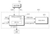
도 3은 본 발명의 실시 예에 따른 액정 디스플레이 장치를 나타내는 도면이고, 도 4는 인쇄회로보드에 실장된 TMIC, 데이터 드라이버 및 커넥터의 접속 구조를 나타내는 도면이다.3 is a diagram illustrating a liquid crystal display device according to an exemplary embodiment of the present invention, and FIG. 4 is a diagram illustrating a connection structure of a TMIC, a data driver, and a connector mounted on a printed circuit board.
도 3 및 도 4를 참조하면, 본 발명의 실시 예에 따른 액정 디스플레이 장치는 화상을 표시하는 액정 패널(100)과, 상기 액정 패널(100)에 광을 공급하는 백라이트 유닛(미도시, Back Light Unit) 및 구동 회로부를 포함하여 구성된다.3 and 4, a liquid crystal display device according to an exemplary embodiment of the present invention includes a
액정 패널(100)은 상부 기판(컬러필터 어레이 기판), 하부 기판(TFT 어레이 기판) 및 상부 기판과 하부 기판 사이에 개재된 액정층을 포함한다. 이러한, 액정 패널(100)의 하부 기판에는 복수의 게이트 라인 및 데이터 라인이 상호 교차하도록 형성되어 있으며, 복수의 게이트 라인 및 데이터 라인에 의해 복수의 픽셀이 정의된다. 복수의 픽셀은 매트릭스 형태로 배열되며, 각 픽셀에는 스위칭 소자인 TFT, 스토리지 커패시터, 픽셀 전극 및 공통 전극이 형성된다.The
액정 패널(100)이 TN(Twisted Nematic) 모드 및 VA(Vertical Alignment) 모드와 같이 수직 전계를 이용하여 화상을 표시하는 경우에는 상기 공통 전극이 상부 기판에 형성된다.When the
한편, 액정 패널(100)이 IPS(In Plane Switching) 모드 또는 FFS(Fringe Field Switching)와 같이 수평 전계 또는 프린지 필드를 이용하여 화상을 표시하는 경우에는 상기 공통 전극이 하부 기판에 형성된다.Meanwhile, when the
이러한, 픽셀 전극에 공급된 데이터 전압과 공통 전극에 공급된 공통 전압(Vcom)에 의해 형성된 전계로 액정층을 배열하여 백라이트 유닛에서 조사되는 광의 투과율을 조절함으로써 화상을 표시한다.The image is displayed by arranging the liquid crystal layer by an electric field formed by the data voltage supplied to the pixel electrode and the common voltage Vcom supplied to the common electrode to adjust the transmittance of light emitted from the backlight unit.
백라이트 유닛은 액정 패널(100)에 공급되는 광을 생성하는 광원과 광 효율을 향상시키기 위한 복수의 광학 부재를 포함한다. 광원은 CCFL(Cold Cathode Fluorescent Lamp), EEFL(External Electrode Fluorescent Lamp) 또는 LED(Light Emitting Diode)가 이용될 수 있다. 복수의 광학 부재는 라이트 가이드 패널(LGP: Light Guide Panel), 확산 필름, 프리즘 시트, DBEF(Dual Brightness Enhancement Film)를 포함할 수 있다.The backlight unit includes a light source for generating light supplied to the
구동 회로부는 게이트 드라이버(130), 복수의 데이터 드라이버(300), 전원 공급부(400, PMIC) 및 하나의 TMIC(600, single TMIC)를 포함한다.The driving circuit unit includes a
도 3에서는 TMIC(600)와 2개의 데이터 드라이버(300)가 PCB(200)에 실장된 것을 일 예로 나타낸 것으로, 액정 패널(100)의 화면 크기가 증가되면 이에 비례하여 데이터 드라이버(300)의 개수도 증가할 수 있다. TMIC(600)는 2개의 데이터 드라이버(300) 사이에 배치될 수도 있고, PCB(200)의 일측에 치우쳐 배치될 수도 있다.In FIG. 3, the
본 발명의 액정 디스플레이 장치는 TMIC(600)가 배치되는 위치에 상관 없이, 하나의 TMIC(600)가 EPI 패킷을 생성하고, 생성된 EPI 패킷을 복수의 데이터 드라이버(600)에 공급하여 액정 패널(100)에 화상을 표시하는 것으로 TMIC의 개수를 줄일 수 있다.In the liquid crystal display device of the present invention, regardless of the position where the
액정 패널(100)은 화상이 표시되는 표시 영역(110)과, 라인 및 패드가 형성된 비표시 영역(120)을 포함하며, 구동 회로부 중에서 게이트 드라이버(130)는 GIP 방식으로 비표시 영역(120)에 형성될 수 있다.The
게이트 드라이버(130)는 TMIC(600)에서 공급되는 GIP 제어 신호 및 전원 공급부(400)에서 공급되는 GIP 입력 신호(GIP input signal)을 이용하여 스캔 신호를 생성한다. 이후, 액정 패널(100)에 형성된 복수의 게이트 라인에 스캔 신호를 순차적으로 공급하여 액정 패널(100)에 형성된 복수의 픽셀을 스위칭 한다.The
TMIC(600), 복수의 데이터 드라이버(300) 및 전원 공급부(400)는 PCB(200)에 실장된다. PCB(200)에는 외부로부터 입력된 LVDS를 TMIC(600)로 전송하기 위한 커넥터(500)가 형성되어 있다. 또한, PCB(200)에는 TMIC(600)의 구동 및 감마전압의 생성을 위한 컨트롤 데이터가 저장된 EEPROM(700)이 형성되어 있다.The
PCB(200)에는 커넥터(500)와 TMIC(600)를 접속시키는 제1 라인들(210, LVDS 라인)이 형성되어 있고, TMIC(600)와 복수의 데이터 드라이버(300)를 접속시키는 제2 라인들(220, EPI 패킷 라인)이 형성되어 있다.The
영상 신호 및 제어 신호가 포함된 LVDS는 커넥터(500)에 입력되고, 제1 라인들(210)을 경유하여 TMIC(600)에 입력된다. TMIC(600)에서 생성된 EPI 패킷은 제2 라인들(620)을 경유하여 복수의 데이터 드라이버(300)에 공급된다.The LVDS including the image signal and the control signal is input to the
상술한 설명 및 도면에서는 영상 신호 및 제어 신호가 LVDS(low voltage differential signal) 인터페이스 방식으로 TMIC(600)에 입력되는 것으로 설명하였나 이는 본 발명의 여러 실시 예들 중에서 하나를 설명한 것이다. 본 발명의 다른 실시 예로서, AiPi(Advanced Intra Panel Interface), MIPI(Mobile Industry Processor Interface), eDP(embedded Display Port) 인터페이스 방식을 이용하여 영상 신호 및 제어 신호가 TMIC(600)에 입력될 수 있다.In the above description and the drawings, the image signal and the control signal have been described as being input to the
도 5는 TMIC의 구성을 나타내는 도면이다.5 is a diagram illustrating a configuration of a TMIC.
도 5를 참조하면, TMIC(600)는 타이밍 컨트롤러(610)와 데이터 드라이버(620)가 결합된 것이다. TMIC(600)는 메모리 소자인 EEPROM(700)과 연결되고, EEPROM(700)로부터 TMIC(600)의 구동을 위한 제어신호 및 감마 전압 제어를 위한 감마 제어 데이터를 로딩하여 구동한다.Referring to FIG. 5, the
TMIC(600)에 포함된 타이밍 컨트롤러(610)는 EPI 패킷(Embedded point to point interface packet)을 생성한다. 그리고, TMIC(600)에 포함된 데이터 드라이버(620)는 액정 패널(100)에 형성된 데이터 라인에 공급되는 데이터 전압을 생성한다. 이때, TMIC(600)에 포함된 데이터 드라이버(620)는 전체 데이터 라인 중에서 일부분에 해당하는 데이터 라인(예로서, 전체 데이터 라인 중에서 1/3에 해당하는 데이터 라인)에 공급되는 데이터 전압을 생성한다.The
TMIC(600)에 포함된 타이밍 컨트롤러(610)는 LVSD에 포함된 영상 신호 및 제어 신호를 EPI 패킷(Embedded point to point interface packet)으로 변환한다.The
TMIC(600)는 EPI 패킷을 복수의 데이터 드라이버(300)에 공급하기 위해서 EPI 출력부(630, EPI TX)를 포함하며, EPI 출력부(630)와 접속된 제2 라인들(220)을 통해 포인트-투-포인트(point-to-point) 방식으로 EPI 패킷을 복수의 데이터 드라이버(300)에 공급한다.The
상술한 설명 및 도면에서는 EPI(Embedded point to point interface packet) 인터페이스 방식으로 영상 신호 및 제어 신호가 하나의 TMIC(600)에서 복수의 데이터 드라이버(300)로 공급되는 것으로 설명하였나 이는 본 발명의 여러 실시 예들 중에서 하나를 설명한 것이다. 본 발명의 다른 실시 예로서, AVDS(Advanced Voltage Differential Signaling), ACDS(Advanced Current Differential Signaling), RSDS(Reduced Swing Differential Signaling), TTL(Transistor-Transistor Logic), eRVDS(Enhanced Reduced Swing Differential Signaling) 인터페이스 방식을 이용하여 영상 신호 및 제어 신호가 하나의 TMIC(600)에서 복수의 데이터 드라이버(300)로 입력될 수 있다.In the above description and drawings, it has been described that an image signal and a control signal are supplied from a
도 6은 TMIC에 포함된 데이터 드라이버 및 별도로 구비된 데이터 드라이버를 나타내는 도면이다.6 is a diagram illustrating a data driver included in a TMIC and a data driver provided separately.
도 6을 참조하면, TMIC(600)에 포함된 데이터 드라이버(620) 및 PCB(200)에 별도의 구성으로 구비된 복수의 데이터 드라이버(300)는 감마전압(GMA)을 이용하여 디지털 이미지 데이터를 아날로그 데이터 전압으로 변환하고, 데이터 전압을 액정 패널(100)의 픽셀에 공급한다.Referring to FIG. 6, the
TMIC(600)에 포함된 데이터 드라이버(620)는 타이밍 컨트롤러(610)로부터 직접 영상 데이터 및 제어신호를 공급받아 디지털 이미지 데이터를 아날로그의 데이터 전압으로 변환한 후, 액정 패널(100)의 복수의 데이터 라인에 데이터 전압을 공급하게 된다.The
한편, 복수의 데이터 드라이버(300)는 TMIC(600)에서 공급되는 EPI 패킷에 기초하여 디지털 이미지 데이터를 아날로그의 데이터 전압으로 변환한 후, 액정 패널(100)의 복수의 데이터 라인에 데이터 전압을 공급하게 된다.Meanwhile, the plurality of
이러한, 데이터 드라이버(620, 300)는 쉬프트 레지스터(621), 래치부(622), DA 컨버터(623), 출력 버퍼부(624) 및 감마전압 생성부(625)를 포함한다.The
쉬프트 레지스터(621)는 입력된 프리앰블 신호, 클럭 및 제어 신호를 이용하여 샘플링 신호를 생성하고, 샘플링 신호를 래치부(622)에 공급한다. 쉬프트 레지스터부(621)에 포함된 n개의 쉬프트 레지스터들은 소스 스타트 펄스(SSP)를 소스 샘플링 클럭신호(SSC)에 따라 순차적으로 쉬프트 시켜 샘플링신호로 출력한다.The
래치부(622)는 쉬프트 레지스터(621)로부터 공급된 샘플링신호에 응답하여 디지털 데이터(Data)를 순차적으로 래치하여, 1라인 분의 데이터를 DA 컨버터(623)에 공급한다. 이를 위해, 래치부(622)는 n개의 디지털 이미지 데이터를 래치하기 위해 n개의 래치들로 구성되고, n개의 래치들 각각은 디지털 이미지 데이터의 비트 수에 대응하는 크기를 갖는다.The
DA 컨버터(623)은 래치부(622)로부터의 디지털 이미지 데이터(image data)를 아날로그 이미지 데이터 즉, 데이터 전압으로 변환하여 출력 버퍼부(624)에 공급한다.The
DA 컨버터(623)는 래치부(622)로부터의 디지털 데이터(Data)를 정극성 및 부극성의 아날로그 데이터 전압으로 변환하여 출력하게 된다. 이를 위하여, DA 컨버터(623)는 래치부(622)에 공통 접속된 P(Positive) 디코딩부(미도시) 및 N(Negative) 디코딩부(미도시)와, P 디코딩부 및 N 디코딩부의 출력신호를 선택하기 위한 멀티플렉서(MUX)를 구비한다.The
도 7은 본 발명의 실시 예에 따른 액정 디스플레이 장치의 감마전압 생성부를 나타내는 도면이다.7 is a diagram illustrating a gamma voltage generator of a liquid crystal display according to an exemplary embodiment of the present invention.
도 7을 결부하면, 감마전압 생성부(625)는 타이밍 컨트롤러(610)에서 직접 공급되거나 또는 EPI 패킷에 포함되어 공급되는 패킷 감마 데이터를 이용하여 디지털 이미지 데이터(image data)를 데이터 전압으로 변환 시 이용되는 감마전압(GMA)를 생성한다. 이때, 감마전압은 제1 감마전압(GMA1) 내지 제10 감마전압(GMA10)으로 생성되고, 생성된 감마전압은 DA 컨버터(623)에 공급되어 디지털 이미지 데이터가 아날로그 데이터 전압으로 변환된다.Referring to FIG. 7, the
이러한, 감마전압 생성부(625)는 구동 전압(VDD)과 기저 전압(GND) 사이에 직렬로 접속되는 다수의 저항(R)을 포함한다. 다수의 저항은 스트링(string)으로 구성되고, 입력단 및 출력단에 사이에 직렬로 접속되도록 구성된다.The
다수의 저항 사이의 노드를 통해 다수의 저항 값에 따라 서로 다른 전압 값을 가지는 10단계의 제1 감마전압(GMA1) 내지 제10 감마전압(GMA10)이 생성된다.The first gamma voltage GMA1 to the tenth gamma voltage GMA10 having ten different voltage values are generated through the nodes between the plurality of resistors.
또한, 감마전압 생성부(625)는 다수의 저항 사이의 노드에 접속되도록 형성되어 입력된 감마 컨트롤 신호(Gamma packet)에 따라 복수의 감마전압 중 어느 하나의 감마전압을 선택적으로 출력시키는 복수의 디코더를 포함할 수 있다.In addition, the gamma
여기서, 제1 감마전압(GMA1) 내지 제10 감마전압(GMA10) 중에서 제1 감마전압(GMA1) 내지 제5 감마전압(GMA5)는 정극성(+)의 데이터 전압을 위한 하이 감마전압(HIGH GMA)으로 생성될 수 있다. 한편, 제1 감마전압(GMA1) 내지 제10 감마전압(GMA10) 중에서 제6 감마전압(GMA6) 내지 제10 감마전압(GMA10)는 부극성(-)의 데이터 전압을 위한 로우 감마전압(LOW GMA)으로 생성될 수 있다.The first gamma voltage GMA1 to the fifth gamma voltage GMA5 of the first gamma voltage GMA1 to the tenth gamma voltage GMA10 may be a high gamma voltage for a positive data voltage. Can be generated). Meanwhile, among the first gamma voltages GMA1 to 10th gamma voltage GMA10, the sixth gamma voltage GMA6 to the tenth gamma voltage GMA10 may be a low gamma voltage for a negative data voltage. Can be generated).
감마전압 생성부(625)를 데이터 드라이버(620, 300) 내부에 형성함으로써, PCB(200)에 형성되는 라인의 개수를 줄여 PCB(200)의 면적을 감소시킬 수 있다.By forming the
다시 도 6을 참조하면, DA 컨버터(623)는 감마전압 생성부(625)로부터의 정극성 감마전압들(GMA1 ~ GMA5)을 이용하여 디지털 이미지 데이터를 정극성 데이터 전압으로 변환하게 된다. 또한, DA 컨버터(623)는 감마전압 생성부(625)로부터의 부극성 감마전압들(GMA6 ~ GMA10)을 이용하여 디지털 이미지 데이터를 부극성 데이터 전압으로 변환하게 된다.Referring back to FIG. 6, the
출력 버퍼부(624)는 액정 패널(100)에 형성된 데이터 라인과 접속되면, 각 데이터 라인으로 데이터 전압을 출력한다.When the
출력 버퍼부(624)에 포함되는 n개의 출력버퍼들은 n개의 데이터라인들에 직렬로 각각 접속된 전압 추종기(Voltage follower) 등으로 구성된다. 이러한 출력버퍼들은 DA 컨버터(623)로부터의 아날로그 데이터들을 신호 완충하여 액정 패널(100)에 형성된 데이터 라인들에 공급하게 된다.The n output buffers included in the
여기서, TMIC(600)에 포함된 데이터 드라이버(610) 및 PCB(200)에 별도로 실장된 복수의 데이터 드라이버(300)는 액정 패널(100)에 형성된 n개의 데이터 라인들을 일정 개수로 분할하여 데이터 전압을 공급하게 된다.Here, the
예로서, PCB(200)에 TMIC(600)와 2개의 데이터 드라이버(300)가 실장된 경우, 하나의 LCM에 3개의 데이터 드라이버가 구비되어 n개의 데이터 라인을 1/3씩 분할하여 데이터 전압을 공급하게 된다.For example, when the
도 8 및 도 9는 본 발명의 실시 예에 따른 구동방법을 설명한 것으로, TMIC에서 데이터 드라이버로 전송되는 EPI 패킷을 나타내는 도면이고, 도 10은 본 발명의 실시 예에 따른 구동방법에 적용되는 패킷 감마 데이터를 나타내는 도면이다.8 and 9 illustrate a driving method according to an embodiment of the present invention, which shows an EPI packet transmitted from a TMIC to a data driver, and FIG. 10 is a packet gamma applied to the driving method according to an embodiment of the present invention. It is a figure which shows data.
이하, 도 8 내지 도 10을 결부하여, TMIC에서 데이터 드라이버로 전송되는 EPI 패킷과 패킷 감마 데이터에 대하여 상세히 설명하기로 한다.8 to 10, the EPI packet and the packet gamma data transmitted from the TMIC to the data driver will be described in detail.
EPI 패킷은 TMIC(600)의 타이밍 컨트롤러(610)에서 생성되며, EPI 출력부(630)를 통해 복수의 데이터 드라이버(300)에 공급된다. EPI 패킷에는 복수의 데이터 드라이버(300)의 제어를 위한 제어 신호(control signal), 감마전압을 생성을 위한 패킷 감마 데이터 및 RGB 영상 데이터가 포함되어 있다.The EPI packet is generated by the
TMIC(600)의 타이밍 컨트롤러(610)는 외부로부터 입력된 디지털 이미지 데이터를 정렬하고, 디지털 이미지 데이터를 RGB_DATA 패킷으로 구성하여 EPI 패킷에 포함시킨다. 그리고, 제2 라인들(220, EPI 패킷 라인)을 통해 EPI 패킷을 PCB(200)에 별도로 실장된 복수의 데이터 드라이버(300)에 공급한다.The
TMIC(600)의 타이밍 컨트롤러(610)는 EEPROM(700)에 저장된 감마 제어 데이터를 로딩하여, 감마전압의 생성을 위한 패킷 감마 데이터를 생성하고, 생성된 패킷 감마 데이터를 EPI 패킷에 포함시킨다. 그리고, 제2 라인(620, EPI 패킷 라인)을 통해 패킷 감마 데이터를 포함하는 EPI 패킷을 복수의 데이터 드라이버(300)에 공급한다.The
EPI 패킷은 복수의 패킷으로 구성되며, 각각의 패킷은 일정 비트 수, 일 예로서 22비트의 크기를 가지도록 구성될 수 있다.The EPI packet is composed of a plurality of packets, and each packet may be configured to have a certain number of bits, for example, 22 bits.
복수의 패킷은 프리앰블 패킷, 컨트롤 스타트(CTR_START) 패킷, 복수의 컨트롤 패킷(CTR1 ~ CTR2), 패킷 감마 데이터, 데이터 스타트 패킷(DATA_START) 및 이미지 데이터(RGB_DATA) 패킷을 포함하며, 상기 패킷들이 모여 하나의 EPI 패킷을 구성하게 된다.The plurality of packets include a preamble packet, a control start packet (CTR_START) packet, a plurality of control packets (CTR1 to CTR2), packet gamma data, a data start packet (DATA_START), and an image data (RGB_DATA) packet. Will construct an EPI packet.
여기서, 패킷 감마 데이터는 데이터 드라이버(610, 300)에서 디지털 이미지 데이터를 아날로그 데이터 전압으로 변환 시 이용되는 제1 감마전압(GMA1) 내지 제10 감마전압(GMA10)의 생성을 위한 제어 신호이다.Here, the packet gamma data is a control signal for generating the first gamma voltage GMA1 to the tenth gamma voltage GMA10 used when the
컨트롤 신호(control signal)들은 TMIC(600)의 초기화를 위한 프리앰블(Preamble) 신호, 클럭(CLK), EIP 패킷 시작 지시(CTR_START) 신호, 데이터 인에이블(Data Enable: DE) 신호, 소스 출력 신호(Source Output Enable: SOE), 소스 출력 폭 신호(SOE width), 극성신호(Polarity: POL), 게이트 스타트 펄스(Gate Start Pulse: GSP) 신호, 감마 버퍼 인에이블(GMAENB1, GMAENB2) 신호, 이미지 데이터 시작(DATA_START) 신호 및 패킷 감마 데이터를 포함한다.The control signals include a preamble signal, a clock CLK, an EIP packet start indication (CTR_START) signal, a data enable (DE) signal, and a source output signal for initialization of the
상기 프리앰블(Preamble) 신호는 프리앰블 패킷에 인코딩 되고, 그 이외의 제어 신호들은 복수의 컨트롤 패킷들(CTR1 ~ CTR2)에 인코딩 되어 복수의 데이터 드라이버(300)에 공급된다.The preamble signal is encoded in the preamble packet, and other control signals are encoded in the plurality of control packets CTR1 to CTR2 and supplied to the plurality of
복수의 데이터 드라이버(300)에서 생성되는 제1 감마전압(GMA1) 내지 제10 감마전압(GMA10)의 생성을 위한 감마 제어 신호는 별도의 패킷 감마 데이터에 인코딩 되어 EPI 패킷에 포함된다. 이와 같이, 제1 감마전압(GMA1) 내지 제10 감마전압(GMA10)을 생성하기 위한 패킷 감마 데이터를 EPI 패킷에 포함시켜 복수의 데이터 드라이버(300)로 전송할 수 있다.Gamma control signals for generating the first gamma voltages GMA1 to 10th gamma voltage GMA10 generated by the
상기 이미지 데이터(image data)는 RGB 이미지 데이터로 구성되며, 상기 RGB 이미지 데이터가 22비트의 RGB_DATA 패킷에 시리얼로 인코딩 되어, 복수의 데이터 드라이버(300)에 공급된다.The image data is composed of RGB image data, and the RGB image data is serially encoded in a 22-bit RGB_DATA packet and supplied to the plurality of
본 발명의 실시 예에 따른 액정 디스플레이 장치는 PCB(200)에 복수의 TMIC가 적용되었던 것을 하나의 TMIC(600)와 복수의 데이터 드라이버(300)로 변경하여 제조비용을 절감시킬 수 있다.In the liquid crystal display device according to the embodiment of the present invention, a plurality of TMICs are applied to the
구체적으로, 15.6인치의 화면 구동하기 위해서, LVDS 방식의 TMIC를 3개 적용했던 것을 본 발명과 같이 TMIC(600)와 2개의 데이터 드라이버(300)를 적용하면 종래 기술대비 전체 드라이브 IC 비용을 11.7% 절감시킬 수 있다.Specifically, in order to drive a 15.6-inch screen, three TMICs of LVDS type are applied. When the
Build-up PCB는 다양한 미세 홀(hole)을 형성하는 기술을 적용하여, via hole로 층과 층 사이의 접속을 이루면서 각 레이어의 어레이를 가공하여 다층이 형성된 PCB이다. Build-up PCB가 고가이지만 한정된 PCB 면적 안에 다수의 라인의 형성하기 위해서는 Build-up PCB를 사용할 수 밖에 없었다. 반면, MLB(multi layer board) PCB는 내부 회로 층을 미리 형성한 뒤 레이어가 적층된 PCB로써, Build-up PCB 대비 50%의 저렴한 비용으로 제조할 수 있다.Build-up PCB is a PCB with multiple layers formed by applying array technology to form various holes. Although build-up PCBs are expensive, build-up PCBs have to be used to form multiple lines within a limited PCB area. On the other hand, MLB (multi layer board) PCB is a layered PCB after forming the internal circuit layer in advance, it can be manufactured at a 50% lower cost than the build-up PCB.
본 발명의 실시 예에 따른 액정 디스플레이 장치는 PCB(200)에 TMIC(600)를 형성하여 LVDS를 공급하기 위한 라인을 수를 감소시킬 수 있다. 이를 통해, 본 발명의 실시 예에 따른 액정 디스플레이 장치는 구동 회로부가 실장되는 고가의 build-up PCB를 저가의 MLB PCB 로 변경하여 제조비용을 절감시킬 수 있다.In the liquid crystal display device according to the exemplary embodiment of the present invention, the
본 발명이 속하는 기술분야의 당 업자는 상술한 본 발명이 그 기술적 사상이나 필수적 특징을 변경하지 않고서 다른 구체적인 형태로 실시될 수 있다는 것을 이해할 수 있을 것이다. 그러므로, 이상에서 기술한 실시 예들은 모든 면에서 예시적인 것이며 한정적인 것이 아닌 것으로 이해해야만 한다.Those skilled in the art to which the present invention pertains will understand that the above-described present invention can be implemented in other specific forms without changing the technical spirit or essential features. Therefore, it is to be understood that the embodiments described above are exemplary in all respects and not restrictive.
본 발명의 범위는 상기 상세한 설명보다는 후술하는 특허청구범위에 의하여 나타내어지며, 특허청구범위의 의미 및 범위 그리고 그 등가 개념으로부터 도출되는 모든 변경 또는 변형된 형태가 본 발명의 범위에 포함되는 것으로 해석되어야 한다.The scope of the present invention is shown by the following claims rather than the detailed description, and all changes or modifications derived from the meaning and scope of the claims and their equivalent concepts should be construed as being included in the scope of the present invention. do.
100: 액정 패널110: 표시 영역
120: 비표시 영역130: 게이트 드라이버
200: 인쇄회로보드210: 라인
300: 데이터 드라이버400: 전원 공급부
500: 커넥터600: TMIC
610: 타이밍 컨트롤러612: EPI 출력부
620: 데이터 드라이버621: 쉬프트 레지스터부
622: 래치부623: DA 컨버터
624: 출력 버퍼부625: 감마전압 생성부
700: EEPROM100: liquid crystal panel 110: display area
120: non-display area 130: gate driver
200: printed circuit board 210: line
300: data driver 400: power supply
500: connector 600: TMIC
610: timing controller 612: EPI output
620: data driver 621: shift register section
622: latch portion 623: DA converter
624: output buffer unit 625: gamma voltage generator
700: EEPROM
Claims (13)
Translated fromKorean상기 액정 패널의 비표시 영역에 형성된 게이트 드라이버;
타이밍 컨트롤러와 제 1 데이터 드라이버를 포함하는 TMIC(timing controller merged IC);
상기 TMIC에서 공급된 패킷 데이터에 의해 구동되는 복수의 제 2 데이터 드라이버; 및
전원 공급부를 실장하는 인쇄회로보드를 포함하며,
상기 TMIC에 포함된 타이밍 컨트롤러는 제 1 인터페이스 방식에 따라 입력되는 영상 신호와 제어 신호를 수신하고, 수신된 영상 신호와 제어 신호를 상기 제 1 인터페이스 방식과 다른 제 2 인터페이스 방식에 따른 상기 패킷 데이터로 변환하여 상기 복수의 제 2 데이터 드라이버 각각에 공급하며,
상기 TMIC에 포함된 제 1 데이터 드라이버는 상기 TMIC에 포함된 타이밍 컨트롤러로부터 상기 영상 신호 및 제어 신호를 직접적으로 공급받는, 액정 디스플레이 장치.Liquid crystal panels;
A gate driver formed in the non-display area of the liquid crystal panel;
A timing controller merged IC (TMIC) including a timing controller and a first data driver;
A plurality of second data drivers driven by packet data supplied from the TMIC; And
It includes a printed circuit board for mounting the power supply,
The timing controller included in the TMIC receives an image signal and a control signal input according to a first interface method, and converts the received image signal and control signal into the packet data according to a second interface method different from the first interface method. Converts and supplies each of the plurality of second data drivers,
And a first data driver included in the TMIC directly receives the image signal and the control signal from a timing controller included in the TMIC.
상기 제 2 인터페이스 방식은 EPI(Embedded point to point interface), AVDS(Advanced Voltage Differential Signaling), ACDS(Advanced Current Differential Signaling), RSDS(Reduced Swing Differential Signaling), TTL(Transistor-Transistor Logic) 또는 eRVDS(Enhanced Reduced Swing Differential Signaling)인, 액정 디스플레이 장치.The method of claim 1,
The second interface method includes an embedded point to point interface (EPI), advanced voltage differential signaling (AVDS), advanced current differential signaling (ACDS), reduced swing differential signaling (RSDS), transistor-transistor logic (TTL), or eRVDS (enhanced). Liquid crystal display device, which is Reduced Swing Differential Signaling.
상기 인쇄회로보드는,
상기 제 1 인터페이스 방식에 따라 상기 영상 신호 및 제어 신호를 상기 TMIC에 포함된 타이밍 컨트롤러에 공급하기 위한 제1 라인들; 및
상기 제 2 인터페이스 방식에 따라 상기 TMIC에 포함된 타이밍 컨트롤러로부터 출력되는 상기 패킷 데이터를 상기 복수의 제 2 데이터 드라이버에 공급하기 위한 제2 라인들을 포함하는, 액정 디스플레이 장치.The method of claim 1,
The printed circuit board,
First lines for supplying the image signal and the control signal to a timing controller included in the TMIC according to the first interface scheme; And
And second lines for supplying the packet data output from the timing controller included in the TMIC to the plurality of second data drivers according to the second interface scheme.
상기 인쇄회로보드는 상기 제1 라인들과 상기 제2 라인들을 포함하는 MLB(multi layer board) PCB인, 액정 디스플레이 장치.The method of claim 3, wherein
Wherein the printed circuit board is a multi-layer board (MLB) PCB comprising the first lines and the second lines.
상기 TMIC에 포함된 타이밍 컨트롤러는 감마 전압의 생성을 위한 패킷 감마 데이터를 상기 패킷 데이터에 포함시키는, 액정 디스플레이 장치.The method of claim 1,
And a timing controller included in the TMIC includes packet gamma data for generation of a gamma voltage in the packet data.
상기 인쇄회로보드는,
상기 TMIC의 구동과 감마 전압 제어를 위한 제어신호가 저장된 EEPROM; 및
외부로부터 상기 제 1 인터페이스 방식에 따라 영상 신호 및 제어 신호가 입력되는 커넥터를 더 포함하는, 액정 디스플레이 장치.The method of claim 3, wherein
The printed circuit board,
An EEPROM storing control signals for driving the TMIC and controlling gamma voltage; And
And a connector to which an image signal and a control signal are input from the outside according to the first interface method.
상기 제1 라인들은 상기 TMIC와 상기 커넥터 사이에 연결되며,
상기 제2 라인들은 상기 복수의 제 2 데이터 드라이버 각각과 상기 TMIC 사이에 독립적으로 연결된, 액정 디스플레이 장치.The method of claim 6,
The first lines are connected between the TMIC and the connector,
And the second lines are independently connected between each of the plurality of second data drivers and the TMIC.
상기 TMIC에 포함된 타이밍 컨트롤러는 상기 패킷 데이터를 상기 제 2 복수의 데이터 드라이버로 출력하는 출력부를 포함하는, 액정 디스플레이 장치.The method according to any one of claims 1 to 7,
The timing controller included in the TMIC includes an output unit for outputting the packet data to the second plurality of data drivers.
상기 제 1 인터페이스 방식은 LVDS(low voltage differential signal), AiPi(Advanced Intra Panel Interface), MIPI(Mobile Industry Processor Interface) 또는 eDP(embedded Display Port)이며,
상기 제 2 인터페이스 방식은 EPI(Embedded point to point interface), AVDS(Advanced Voltage Differential Signaling), ACDS(Advanced Current Differential Signaling), RSDS(Reduced Swing Differential Signaling), TTL(Transistor-Transistor Logic) 또는 eRVDS(Enhanced Reduced Swing Differential Signaling)인, 액정 디스플레이 장치.The method of claim 1,
The first interface method is a low voltage differential signal (LVDS), an advanced intra panel interface (AiPi), a mobile industry processor interface (MIPI), or an embedded display port (eDP),
The second interface method includes an embedded point to point interface (EPI), advanced voltage differential signaling (AVDS), advanced current differential signaling (ACDS), reduced swing differential signaling (RSDS), transistor-transistor logic (TTL), or eRVDS (enhanced). Liquid crystal display device, which is Reduced Swing Differential Signaling.
제 1 인터페이스 방식에 따라 영상 신호와 제어 신호를 상기 TMIC에 포함된 타이밍 컨트롤러에 입력하는 단계;
상기 TMIC에 포함된 타이밍 컨트롤러에서 상기 제 1 인터페이스 방식에 따라 입력되는 영상 신호와 제어 신호를 수신하고, 수신된 영상 신호와 제어 신호를 상기 제 1 인터페이스 방식과 다른 제 2 인터페이스 방식에 따른 패킷 데이터로 변환하여 출력하는 단계;
상기 복수의 제 2 데이터 드라이버 각각에서 상기 TMIC에 포함된 타이밍 컨트롤러로부터 출력되는 상기 패킷 데이터를 수신하고, 수신된 패킷 데이터에 기초한 데이터 전압을 액정 패널로 출력하는 단계; 및
상기 TMIC에 포함된 제 1 데이터 드라이버에서 상기 TMIC에 포함된 타이밍 컨트롤러로부터 직접적으로 공급되는 상기 영상 신호 및 제어 신호에 기초한 데이터 전압을 상기 액정 패널로 출력하는 단계를 포함하는, 액정 디스플레이 장치의 구동방법.A driving method of a liquid crystal display device including one TMIC including a timing controller and a first data driver and a plurality of second data drivers,
Inputting an image signal and a control signal to a timing controller included in the TMIC according to a first interface method;
Receives an image signal and a control signal input according to the first interface method in the timing controller included in the TMIC, and converts the received image signal and the control signal into packet data according to a second interface method different from the first interface method. Converting and outputting;
Receiving the packet data output from the timing controller included in the TMIC in each of the plurality of second data drivers, and outputting a data voltage based on the received packet data to a liquid crystal panel; And
Outputting a data voltage based on the image signal and a control signal directly supplied from a timing controller included in the TMIC to the liquid crystal panel in a first data driver included in the TMIC. .
상기 액정 디스플레이 장치는 상기 하나의 TMIC 및 상기 복수의 제 2 데이터 드라이버에 연결된 MLB(multi layer board) PCB를 더 포함하며,
상기 MLB PCB는,
상기 제 1 인터페이스 방식에 따라 상기 영상 신호 및 제어 신호를 상기 TMIC에 포함된 타이밍 컨트롤러에 공급하기 위한 제1 라인들; 및
상기 제 2 인터페이스 방식에 따라 상기 TMIC에 포함된 타이밍 컨트롤러로부터 출력되는 상기 패킷 데이터를 상기 복수의 제 2 데이터 드라이버에 공급하기 위한 제2 라인들을 포함하며,
상기 TMIC에 포함된 타이밍 컨트롤러에서 출력되는 상기 패킷 데이터는 상기 MLB PCB의 제2 라인들을 통해 상기 복수의 제 2 데이터 드라이버 각각에 개별적으로 입력되는, 액정 디스플레이 장치의 구동 방법.The method of claim 10,
The liquid crystal display device further includes a multi-layer board (MLB) PCB connected to the one TMIC and the plurality of second data drivers,
The MLB PCB,
First lines for supplying the image signal and the control signal to a timing controller included in the TMIC according to the first interface scheme; And
And second lines for supplying the packet data output from the timing controller included in the TMIC to the plurality of second data drivers according to the second interface method.
And the packet data output from the timing controller included in the TMIC are individually input to each of the plurality of second data drivers through second lines of the MLB PCB.
상기 TMIC에 포함된 타이밍 컨트롤러는 감마 전압의 생성을 위한 패킷 감마 데이터를 상기 패킷 데이터에 포함시키는, 액정 디스플레이 장치의 구동방법.The method of claim 10,
The timing controller included in the TMIC includes a packet gamma data for generating a gamma voltage in the packet data.
상기 제 1 인터페이스 방식은 LVDS(low voltage differential signal), AiPi(Advanced Intra Panel Interface), MIPI(Mobile Industry Processor Interface) 또는 eDP(embedded Display Port)이며,
상기 제 2 인터페이스 방식은 EPI(Embedded point to point interface), AVDS(Advanced Voltage Differential Signaling), ACDS(Advanced Current Differential Signaling), RSDS(Reduced Swing Differential Signaling), TTL(Transistor-Transistor Logic) 또는 eRVDS(Enhanced Reduced Swing Differential Signaling)인, 액정 디스플레이 장치의 구동방법.The method according to any one of claims 10 to 12,
The first interface method is a low voltage differential signal (LVDS), an advanced intra panel interface (AiPi), a mobile industry processor interface (MIPI), or an embedded display port (eDP),
The second interface method includes an embedded point to point interface (EPI), advanced voltage differential signaling (AVDS), advanced current differential signaling (ACDS), reduced swing differential signaling (RSDS), transistor-transistor logic (TTL), or eRVDS (enhanced). A method of driving a liquid crystal display device, which is Reduced Swing Differential Signaling.
Priority Applications (3)
| Application Number | Priority Date | Filing Date | Title |
|---|---|---|---|
| KR1020120096229AKR101987191B1 (en) | 2012-08-31 | 2012-08-31 | Liquid crystal display device and method for driving the same |
| US13/720,970US9607560B2 (en) | 2012-08-31 | 2012-12-19 | Liquid crystal display device and method for driving the same |
| CN201210567856.8ACN103680432B (en) | 2012-08-31 | 2012-12-24 | Liquid crystal indicator and the method driving this liquid crystal indicator |
Applications Claiming Priority (1)
| Application Number | Priority Date | Filing Date | Title |
|---|---|---|---|
| KR1020120096229AKR101987191B1 (en) | 2012-08-31 | 2012-08-31 | Liquid crystal display device and method for driving the same |
Publications (2)
| Publication Number | Publication Date |
|---|---|
| KR20140028885A KR20140028885A (en) | 2014-03-10 |
| KR101987191B1true KR101987191B1 (en) | 2019-09-30 |
Family
ID=50186893
Family Applications (1)
| Application Number | Title | Priority Date | Filing Date |
|---|---|---|---|
| KR1020120096229AActiveKR101987191B1 (en) | 2012-08-31 | 2012-08-31 | Liquid crystal display device and method for driving the same |
Country Status (3)
| Country | Link |
|---|---|
| US (1) | US9607560B2 (en) |
| KR (1) | KR101987191B1 (en) |
| CN (1) | CN103680432B (en) |
Cited By (1)
| Publication number | Priority date | Publication date | Assignee | Title |
|---|---|---|---|---|
| US12374261B2 (en) | 2023-02-10 | 2025-07-29 | Samsung Display Co., Ltd. | Display device |
Families Citing this family (12)
| Publication number | Priority date | Publication date | Assignee | Title |
|---|---|---|---|---|
| KR102154190B1 (en)* | 2014-05-08 | 2020-09-09 | 삼성전자 주식회사 | Driver integrated circuit comprised of multi-chip and driving method thereof |
| KR101698930B1 (en) | 2014-11-11 | 2017-01-23 | 삼성전자 주식회사 | Display driving device, display device and Opertaing method thereof |
| JP6574369B2 (en) | 2015-10-13 | 2019-09-11 | 株式会社ジャパンディスプレイ | Display device |
| KR102423769B1 (en) | 2015-10-16 | 2022-07-21 | 삼성전자주식회사 | Operating method of receiver, source driver and display driving circuit comprising thereof |
| CN105405384A (en)* | 2015-12-31 | 2016-03-16 | 深圳市华星光电技术有限公司 | Display control circuit and display device |
| KR102512721B1 (en)* | 2016-04-05 | 2023-03-23 | 삼성디스플레이 주식회사 | Display apparatus |
| KR102609948B1 (en)* | 2016-09-30 | 2023-12-04 | 엘지디스플레이 주식회사 | Display panel driving unit, its driving method, and display device including the same |
| KR102576159B1 (en)* | 2016-10-25 | 2023-09-08 | 삼성디스플레이 주식회사 | Display apparatus and driving method thereof |
| KR102389037B1 (en)* | 2017-07-31 | 2022-04-20 | 엘지디스플레이 주식회사 | Driver-ic and display device including the same |
| KR102305235B1 (en)* | 2018-01-29 | 2021-09-27 | 주식회사 자연과사람 | A Controlling Board Having a Structure of Multi Interface |
| KR102545589B1 (en)* | 2018-12-28 | 2023-06-21 | 삼성디스플레이 주식회사 | Display system and method of generating gamma voltages for the same |
| WO2023283775A1 (en)* | 2021-07-12 | 2023-01-19 | 重庆康佳光电技术研究院有限公司 | Panel driving structure, driving method, and display apparatus |
Citations (2)
| Publication number | Priority date | Publication date | Assignee | Title |
|---|---|---|---|---|
| US20060202937A1 (en)* | 2005-03-11 | 2006-09-14 | Himax Technologies, Inc. | Method and apparatus for generating gate control signal of liquid crystal display |
| US20110298812A1 (en)* | 2010-06-02 | 2011-12-08 | Chin-Jui Liu | Seamless Switching Between Graphics Controllers |
Family Cites Families (12)
| Publication number | Priority date | Publication date | Assignee | Title |
|---|---|---|---|---|
| JP3508837B2 (en)* | 1999-12-10 | 2004-03-22 | インターナショナル・ビジネス・マシーンズ・コーポレーション | Liquid crystal display device, liquid crystal controller, and video signal transmission method |
| JP4783890B2 (en)* | 2000-02-18 | 2011-09-28 | 株式会社 日立ディスプレイズ | Liquid crystal display |
| US7098901B2 (en) | 2000-07-24 | 2006-08-29 | Sharp Kabushiki Kaisha | Display device and driver |
| US20060232579A1 (en) | 2005-04-14 | 2006-10-19 | Himax Technologies, Inc. | WOA panel architecture |
| KR101222949B1 (en) | 2005-09-06 | 2013-01-17 | 엘지디스플레이 주식회사 | A driving circuit of liquid crystal display device and a method for driving the same |
| KR100968554B1 (en) | 2008-07-24 | 2010-07-08 | 주식회사 실리콘웍스 | LCM for display panel |
| KR101289642B1 (en) | 2009-05-11 | 2013-07-30 | 엘지디스플레이 주식회사 | Liquid crystal display |
| US20110157103A1 (en) | 2009-12-28 | 2011-06-30 | Himax Technologies Limited | Display Device and Driving Circuit |
| US8665606B2 (en) | 2010-07-16 | 2014-03-04 | Mediatek Inc. | Electronic device having circuit board with co-layout design of multiple connector placement sites and related circuit board thereof |
| CN102402089A (en) | 2011-12-02 | 2012-04-04 | 深圳市华星光电技术有限公司 | Liquid crystal display device and method for repairing disconnected lines |
| US9305510B2 (en) | 2012-04-26 | 2016-04-05 | Shenzhen China Star Optoelectronics Technology Co., Ltd. | LCD driving module, LCD device, and method for driving LCD |
| CN102637419B (en) | 2012-04-26 | 2014-07-02 | 深圳市华星光电技术有限公司 | Liquid crystal display drive module, liquid crystal display device and liquid crystal display drive method |
- 2012
- 2012-08-31KRKR1020120096229Apatent/KR101987191B1/enactiveActive
- 2012-12-19USUS13/720,970patent/US9607560B2/enactiveActive
- 2012-12-24CNCN201210567856.8Apatent/CN103680432B/enactiveActive
Patent Citations (2)
| Publication number | Priority date | Publication date | Assignee | Title |
|---|---|---|---|---|
| US20060202937A1 (en)* | 2005-03-11 | 2006-09-14 | Himax Technologies, Inc. | Method and apparatus for generating gate control signal of liquid crystal display |
| US20110298812A1 (en)* | 2010-06-02 | 2011-12-08 | Chin-Jui Liu | Seamless Switching Between Graphics Controllers |
Cited By (1)
| Publication number | Priority date | Publication date | Assignee | Title |
|---|---|---|---|---|
| US12374261B2 (en) | 2023-02-10 | 2025-07-29 | Samsung Display Co., Ltd. | Display device |
Also Published As
| Publication number | Publication date |
|---|---|
| CN103680432B (en) | 2017-03-01 |
| CN103680432A (en) | 2014-03-26 |
| KR20140028885A (en) | 2014-03-10 |
| US20140062983A1 (en) | 2014-03-06 |
| US9607560B2 (en) | 2017-03-28 |
Similar Documents
| Publication | Publication Date | Title |
|---|---|---|
| KR101987191B1 (en) | Liquid crystal display device and method for driving the same | |
| US9087474B2 (en) | Liquid crystal display device and driving method thereof | |
| KR101279351B1 (en) | Timing controller and liquid crystal display using the same | |
| KR101904277B1 (en) | Iquid crystal display apparatus | |
| CN101950547B (en) | LCD panel display driving system and flexible circuit board thereof | |
| US8446400B2 (en) | Driving apparatus for driving a display panel and source driver thereof | |
| US20080218647A1 (en) | Liquid crystal display device | |
| US8970472B2 (en) | Apparatus for driving light emitting diode array and liquid crystal display device using the same | |
| KR20170062573A (en) | Display device | |
| KR102113986B1 (en) | Gate driver and display device comprising the same | |
| KR101961367B1 (en) | Liquid crystal display device and method for driving the same | |
| CN103295544B (en) | Liquid crystal display | |
| KR102596604B1 (en) | Drive ic and display device using the same | |
| KR101968178B1 (en) | Timing control unit and liquid crystal display device comprising the same | |
| KR101761407B1 (en) | Liquid Crystal Display Device | |
| KR102511310B1 (en) | Back Light Unit and Liquid Crystal Display Device using the same | |
| KR102458522B1 (en) | Gate Driving Circuit for Display Device and Display Device having the same | |
| KR20150072705A (en) | Display device | |
| KR20120072681A (en) | Display device | |
| KR20120072707A (en) | Display device and driving method thereof | |
| KR20120065189A (en) | Timing controller of liquid crystal display device | |
| KR20070079486A (en) | Drive device and display device including same | |
| KR101061063B1 (en) | ROM Data Input System and Input Method of Printed Circuit Board for Liquid Crystal Display and Printed Circuit Board for Liquid Crystal Display | |
| KR20130031091A (en) | Liquid crystal display device | |
| KR20070083035A (en) | Display device and manufacturing method thereof |
Legal Events
| Date | Code | Title | Description |
|---|---|---|---|
| PA0109 | Patent application | Patent event code:PA01091R01D Comment text:Patent Application Patent event date:20120831 | |
| PG1501 | Laying open of application | ||
| A201 | Request for examination | ||
| PA0201 | Request for examination | Patent event code:PA02012R01D Patent event date:20170725 Comment text:Request for Examination of Application Patent event code:PA02011R01I Patent event date:20120831 Comment text:Patent Application | |
| E902 | Notification of reason for refusal | ||
| PE0902 | Notice of grounds for rejection | Comment text:Notification of reason for refusal Patent event date:20181022 Patent event code:PE09021S01D | |
| E701 | Decision to grant or registration of patent right | ||
| PE0701 | Decision of registration | Patent event code:PE07011S01D Comment text:Decision to Grant Registration Patent event date:20190530 | |
| GRNT | Written decision to grant | ||
| PR0701 | Registration of establishment | Comment text:Registration of Establishment Patent event date:20190603 Patent event code:PR07011E01D | |
| PR1002 | Payment of registration fee | Payment date:20190604 End annual number:3 Start annual number:1 | |
| PG1601 | Publication of registration | ||
| PR1001 | Payment of annual fee | Payment date:20220516 Start annual number:4 End annual number:4 | |
| PR1001 | Payment of annual fee | Payment date:20230515 Start annual number:5 End annual number:5 | |
| PR1001 | Payment of annual fee | Payment date:20240516 Start annual number:6 End annual number:6 |