KR101985481B1 - Display device and method of manufacturing the same - Google Patents
Display device and method of manufacturing the sameDownload PDFInfo
- Publication number
- KR101985481B1 KR101985481B1KR1020120080004AKR20120080004AKR101985481B1KR 101985481 B1KR101985481 B1KR 101985481B1KR 1020120080004 AKR1020120080004 AKR 1020120080004AKR 20120080004 AKR20120080004 AKR 20120080004AKR 101985481 B1KR101985481 B1KR 101985481B1
- Authority
- KR
- South Korea
- Prior art keywords
- substrate
- display area
- delete delete
- common electrode
- column spacer
- Prior art date
- Legal status (The legal status is an assumption and is not a legal conclusion. Google has not performed a legal analysis and makes no representation as to the accuracy of the status listed.)
- Active
Links
- 238000004519manufacturing processMethods0.000titleabstractdescription14
- 239000000758substrateSubstances0.000claimsabstractdescription129
- 125000006850spacer groupChemical group0.000claimsabstractdescription60
- 239000004973liquid crystal related substanceSubstances0.000claimsabstractdescription17
- 239000010410layerSubstances0.000claimsdescription72
- 239000011159matrix materialSubstances0.000claimsdescription36
- 239000000565sealantSubstances0.000claimsdescription29
- 239000010408filmSubstances0.000claimsdescription22
- 239000004020conductorSubstances0.000claimsdescription21
- 239000010409thin filmSubstances0.000claimsdescription18
- 238000000034methodMethods0.000claimsdescription16
- 239000000463materialSubstances0.000claimsdescription6
- 239000004065semiconductorSubstances0.000claimsdescription2
- 239000012044organic layerSubstances0.000claims2
- 230000015572biosynthetic processEffects0.000description6
- 230000000694effectsEffects0.000description3
- 238000002161passivationMethods0.000description2
- 239000011521glassSubstances0.000description1
- 230000002401inhibitory effectEffects0.000description1
- 239000011810insulating materialSubstances0.000description1
- 238000007789sealingMethods0.000description1
- -1specificallySubstances0.000description1
- 229920001187thermosetting polymerPolymers0.000description1
Images


Classifications
- G—PHYSICS
- G02—OPTICS
- G02F—OPTICAL DEVICES OR ARRANGEMENTS FOR THE CONTROL OF LIGHT BY MODIFICATION OF THE OPTICAL PROPERTIES OF THE MEDIA OF THE ELEMENTS INVOLVED THEREIN; NON-LINEAR OPTICS; FREQUENCY-CHANGING OF LIGHT; OPTICAL LOGIC ELEMENTS; OPTICAL ANALOGUE/DIGITAL CONVERTERS
- G02F1/00—Devices or arrangements for the control of the intensity, colour, phase, polarisation or direction of light arriving from an independent light source, e.g. switching, gating or modulating; Non-linear optics
- G02F1/01—Devices or arrangements for the control of the intensity, colour, phase, polarisation or direction of light arriving from an independent light source, e.g. switching, gating or modulating; Non-linear optics for the control of the intensity, phase, polarisation or colour
- G02F1/13—Devices or arrangements for the control of the intensity, colour, phase, polarisation or direction of light arriving from an independent light source, e.g. switching, gating or modulating; Non-linear optics for the control of the intensity, phase, polarisation or colour based on liquid crystals, e.g. single liquid crystal display cells
- G02F1/133—Constructional arrangements; Operation of liquid crystal cells; Circuit arrangements
- G02F1/1333—Constructional arrangements; Manufacturing methods
- G02F1/1339—Gaskets; Spacers; Sealing of cells
- G02F1/13394—Gaskets; Spacers; Sealing of cells spacers regularly patterned on the cell subtrate, e.g. walls, pillars
- G—PHYSICS
- G02—OPTICS
- G02F—OPTICAL DEVICES OR ARRANGEMENTS FOR THE CONTROL OF LIGHT BY MODIFICATION OF THE OPTICAL PROPERTIES OF THE MEDIA OF THE ELEMENTS INVOLVED THEREIN; NON-LINEAR OPTICS; FREQUENCY-CHANGING OF LIGHT; OPTICAL LOGIC ELEMENTS; OPTICAL ANALOGUE/DIGITAL CONVERTERS
- G02F1/00—Devices or arrangements for the control of the intensity, colour, phase, polarisation or direction of light arriving from an independent light source, e.g. switching, gating or modulating; Non-linear optics
- G02F1/01—Devices or arrangements for the control of the intensity, colour, phase, polarisation or direction of light arriving from an independent light source, e.g. switching, gating or modulating; Non-linear optics for the control of the intensity, phase, polarisation or colour
- G02F1/13—Devices or arrangements for the control of the intensity, colour, phase, polarisation or direction of light arriving from an independent light source, e.g. switching, gating or modulating; Non-linear optics for the control of the intensity, phase, polarisation or colour based on liquid crystals, e.g. single liquid crystal display cells
- G02F1/133—Constructional arrangements; Operation of liquid crystal cells; Circuit arrangements
- G02F1/136—Liquid crystal cells structurally associated with a semi-conducting layer or substrate, e.g. cells forming part of an integrated circuit
- G02F1/1362—Active matrix addressed cells
- G02F1/136286—Wiring, e.g. gate line, drain line
- G—PHYSICS
- G02—OPTICS
- G02F—OPTICAL DEVICES OR ARRANGEMENTS FOR THE CONTROL OF LIGHT BY MODIFICATION OF THE OPTICAL PROPERTIES OF THE MEDIA OF THE ELEMENTS INVOLVED THEREIN; NON-LINEAR OPTICS; FREQUENCY-CHANGING OF LIGHT; OPTICAL LOGIC ELEMENTS; OPTICAL ANALOGUE/DIGITAL CONVERTERS
- G02F1/00—Devices or arrangements for the control of the intensity, colour, phase, polarisation or direction of light arriving from an independent light source, e.g. switching, gating or modulating; Non-linear optics
- G02F1/01—Devices or arrangements for the control of the intensity, colour, phase, polarisation or direction of light arriving from an independent light source, e.g. switching, gating or modulating; Non-linear optics for the control of the intensity, phase, polarisation or colour
- G02F1/13—Devices or arrangements for the control of the intensity, colour, phase, polarisation or direction of light arriving from an independent light source, e.g. switching, gating or modulating; Non-linear optics for the control of the intensity, phase, polarisation or colour based on liquid crystals, e.g. single liquid crystal display cells
- G02F1/133—Constructional arrangements; Operation of liquid crystal cells; Circuit arrangements
- G02F1/1333—Constructional arrangements; Manufacturing methods
- G02F1/1335—Structural association of cells with optical devices, e.g. polarisers or reflectors
- G02F1/133509—Filters, e.g. light shielding masks
- G02F1/133512—Light shielding layers, e.g. black matrix
- G—PHYSICS
- G02—OPTICS
- G02F—OPTICAL DEVICES OR ARRANGEMENTS FOR THE CONTROL OF LIGHT BY MODIFICATION OF THE OPTICAL PROPERTIES OF THE MEDIA OF THE ELEMENTS INVOLVED THEREIN; NON-LINEAR OPTICS; FREQUENCY-CHANGING OF LIGHT; OPTICAL LOGIC ELEMENTS; OPTICAL ANALOGUE/DIGITAL CONVERTERS
- G02F2201/00—Constructional arrangements not provided for in groups G02F1/00 - G02F7/00
- G02F2201/12—Constructional arrangements not provided for in groups G02F1/00 - G02F7/00 electrode
- G02F2201/121—Constructional arrangements not provided for in groups G02F1/00 - G02F7/00 electrode common or background
Landscapes
- Physics & Mathematics (AREA)
- Nonlinear Science (AREA)
- Mathematical Physics (AREA)
- Chemical & Material Sciences (AREA)
- Crystallography & Structural Chemistry (AREA)
- General Physics & Mathematics (AREA)
- Optics & Photonics (AREA)
- Engineering & Computer Science (AREA)
- Microelectronics & Electronic Packaging (AREA)
- Liquid Crystal (AREA)
Abstract
Translated fromKoreanDescription
Translated fromKorean표시 장치 및 표시 장치 제조 방법에 관한 것으로서, 공정 단순화가 가능하며 슬림 BM 구조 적용이 가능한 표시 장치 및 표시 장치 제조 방법에 관한 것이다.The present invention relates to a display device and a display device manufacturing method, and more particularly, to a display device and a display device manufacturing method which can simplify a process and can be applied to a slim BM structure.
표시 장치, 특히, 액정 표시 장치는 소형화, 경량화 및 저전력화 등이 가능한 특징으로 인해, 핸드폰, 개인 정보 단말기(Personal Digital Assistant, PDA) 및 휴대용 멀티미디어 재생장치(Portable Multimedia Player, PMP) 등과 같은 소형 제품뿐만 아니라, 중대형 제품인 모니터 및 TV 등에 장착되어 사용되고 있다.2. Description of the Related Art A display device, particularly a liquid crystal display device, can be miniaturized, lightweight, and low in power consumption, and thus can be used as a compact product such as a mobile phone, a personal digital assistant (PDA), and a portable multimedia player In addition, it is used by being attached to a monitor or TV, which is a medium and large-sized product.
이러한, 표시 장치는 실질적으로 영상을 표시하는 표시 영역과 배선과 블랙 매트릭스 (Black Matrix, BM) 등이 형성되는 비표시 영역으로 구분되는데, 최근 표시 장치의 소형화 등에 따라 블랙 매트릭스의 폭이 작게 형성되는 슬림(slim) BM의 적용이 증가하고 있다. 그러나, 비표시 영역에 존재하는 공통 전압 라인, 게이트 배선, 쇼트 포인트(short point)의 공간 확보가 이루어져야 하므로, 블랙 매트릭스의 폭을 축소하는데 한계가 존재한다.The display device is divided into a display area for displaying an image and a non-display area in which a wiring and a black matrix (BM) are formed. In recent years, the width of the black matrix is formed to be small Application of slim BM is increasing. However, a space for the common voltage line, the gate wiring, and the short point existing in the non-display area must be ensured, so that there is a limitation in reducing the width of the black matrix.
이에, 본 발명이 해결하려는 과제는 표시 장치에서의 비표시 영역의 폭, 즉, 블랙 매트릭스의 폭을 작게 형성하는 슬림 BM 구조 적용이 가능한 표시 장치 및 표시 장치 제조 방법을 제공하는 것이다.Therefore, a problem to be solved by the present invention is to provide a display device and a display device manufacturing method applicable to a slim BM structure in which a width of a non-display area in a display device, that is, a width of a black matrix is reduced.
본 발명이 해결하려고 하는 다른 과제는 공통 전압 라인과 컬러 필터 기판의 공통 전극 사이의 쇼트 포인트에 대한 별도의 공정을 제거하여, 공정 단순화가 가능한 표시 장치 및 표시 장치 제조 방법을 제공하는 것이다.Another object to be solved by the present invention is to provide a display device and a display device manufacturing method which can simplify the process by eliminating a separate process for the common point between the common voltage line and the common electrode of the color filter substrate.
본 발명의 과제들은 이상에서 언급한 기술적 과제로 제한되지 않으며, 언급되지 않은 또 다른 기술적 과제들은 아래의 기재로부터 당업자에게 명확하게 이해될 수 있을 것이다.The present invention has been made in view of the above problems, and it is an object of the present invention to provide a method of manufacturing the same.
상기 과제를 달성하기 위한 본 발명의 일 실시예에 따른 표시 장치는 서로 대향하고, 표시 영역 및 표시 영역을 둘러싸는 비표시 영역을 포함하는 제1 기판 및 제2 기판, 제1 기판 상의 비표시 영역에 형성되는 공통 전압 라인, 공통 전압 라인 상에 형성되는 하나 이상의 컬럼 스페이서, 제1 기판 상에서 컬럼 스페이서를 커버하도록형성되고, 공통 전압 라인과 전기적으로 연결되는 도전층, 제2 기판 상에 형성되고, 도전층과 전기적으로 연결되는 공통 전극 및 제1 기판과 제2 기판 사이에 개재되는 액정층을 포함한다.According to an aspect of the present invention, there is provided a display device including a first substrate and a second substrate facing each other and including a display region and a non-display region surrounding the display region, At least one column spacer formed on the common voltage line, a conductive layer formed to cover the column spacer on the first substrate and electrically connected to the common voltage line, A common electrode electrically connected to the conductive layer, and a liquid crystal layer interposed between the first substrate and the second substrate.
상기 과제를 달성하기 위한 본 발명의 다른 실시예에 따른 표시 장치는 서로 대향하고, 표시 영역 및 상기 표시 영역을 둘러싸는 비표시 영역을 포함하는 제1 기판 및 제2 기판, 제1 기판 상의 비표시 영역에 형성되는 공통 전압 라인, 공통 전압 라인 상에 형성되고, 공통 전압 라인과 전기적으로 연결되는 도전층, 제2 기판 상에 형성되는 하나 이상의 컬럼 스페이서, 제2 기판 상에서 컬럼 스페이서를 커버하도록형성되고, 도전층과 전기적으로 연결되는 공통 전극 및 제1 기판과 제2 기판 사이에 개재되는 액정층을 포함한다.According to another aspect of the present invention, there is provided a display device including a first substrate and a second substrate facing each other and including a display region and a non-display region surrounding the display region, A common voltage line formed on the common voltage line, a conductive layer formed on the common voltage line and electrically connected to the common voltage line, at least one column spacer formed on the second substrate, and a column spacer formed on the second substrate to cover the column spacer A common electrode electrically connected to the conductive layer, and a liquid crystal layer interposed between the first substrate and the second substrate.
상기 과제를 달성하기 위한 본 발명의 일 실시예에 따른 표시 장치 제조 방법은 기판 상에 블랙 매트릭스 및 컬러 필터를 형성하는 단계, 블랙 매트릭스 및 컬러 필터 상에 오버코팅층을 형성하는 단계, 오버코팅층 상에 제1 컬럼 스페이서 및 제2 컬럼 스페이서를 형성하는 단계 및 오버코팅층 및 제1 컬럼 스페이서 상에 공통 전극을 형성하는 단계를 포함한다.According to an aspect of the present invention, there is provided a method of manufacturing a display device, including: forming a black matrix and a color filter on a substrate; forming an overcoat layer on the black matrix and the color filter; Forming a first column spacer and a second column spacer, and forming a common electrode on the overcoat layer and the first column spacer.
기타 실시예들의 구체적인 사항들은 상세한 설명 및 도면들에 포함되어 있다.The details of other embodiments are included in the detailed description and drawings.
본 발명의 실시예들에 의하면 적어도 다음과 같은 효과가 있다.The embodiments of the present invention have at least the following effects.
즉, 표시 장치에서의 비표시 영역의 폭, 즉, 블랙 매트릭스의 폭을 작게 형성하는 슬림 BM 구조 적용이 가능한 표시 장치 및 표시 장치 제조 방법을 제공할 수 있다.That is, it is possible to provide a display device and a display device manufacturing method which can apply a slim BM structure in which the width of the non-display area in the display device, that is, the width of the black matrix is reduced.
또, 공통 전압 라인과 컬러 필터 기판의 공통 전극 사이의 쇼트 포인트에 대한 별도의 공정을 제거하여, 공정 단순화가 가능한 표시 장치 및 표시 장치 제조 방법을 제공할 수 있다.It is also possible to provide a display device and a display device manufacturing method that can simplify the process by eliminating a separate process for a short point between the common voltage line and the common electrode of the color filter substrate.
본 발명에 따른 효과는 이상에서 예시된 내용에 의해 제한되지 않으며, 더욱 다양한 효과들이 본 명세서 내에 포함되어 있다.The effects according to the present invention are not limited by the contents exemplified above, and more various effects are included in the specification.
도 1 내지 도 6은 본 발명의 다양한 실시예들에 따른 표시 장치의 단면도들이다.
도 7은 본 발명의 일 실시예에 따른 표시 장치 제조 방법의 순서도이다.
도 8 내지 도 12는 본 발명의 일 실시예에 따른 표시 장치 제조 방법을 설명하기 위한 공정별 단면도들이다.1 to 6 are cross-sectional views of a display device according to various embodiments of the present invention.
7 is a flowchart of a method of manufacturing a display device according to an embodiment of the present invention.
8 to 12 are cross-sectional views for explaining a method of manufacturing a display device according to an embodiment of the present invention.
본 발명의 이점 및 특징, 그리고 그것들을 달성하는 방법은 첨부되는 도면과 함께 상세하게 후술되어 있는 실시예들을 참조하면 명확해질 것이다. 그러나 본 발명은 이하에서 개시되는 실시예들에 한정되는 것이 아니라 서로 다른 다양한 형태로 구현될 것이며, 단지 본 실시예들은 본 발명의 개시가 완전하도록 하며, 본 발명이 속하는 기술분야에서 통상의 지식을 가진 자에게 발명의 범주를 완전하게 알려주기 위해 제공되는 것이며, 본 발명은 청구항의 범주에 의해 정의될 뿐이다.BRIEF DESCRIPTION OF THE DRAWINGS The advantages and features of the present invention and the manner of achieving them will become apparent with reference to the embodiments described in detail below with reference to the accompanying drawings. The present invention may, however, be embodied in many different forms and should not be construed as being limited to the embodiments set forth herein. Rather, these embodiments are provided so that this disclosure will be thorough and complete, and will fully convey the scope of the invention to those skilled in the art. Is provided to fully convey the scope of the invention to those skilled in the art, and the invention is only defined by the scope of the claims.
소자(elements) 또는 층이 다른 소자 또는 층"위(on)"로 지칭되는 것은 다른 소자 바로 위에 또는 중간에 다른 층 또는 다른 소자를 개재한 경우를 모두 포함한다. 명세서 전체에 걸쳐 동일 참조 부호는 동일 구성 요소를 지칭한다.It is to be understood that elements or layers are referred to as being " on " other elements or layers, including both intervening layers or other elements directly on or in between. Like reference numerals refer to like elements throughout the specification.
비록 제1, 제2 등이 다양한 구성요소들을 서술하기 위해서 사용되나, 이들 구성요소들은 이들 용어에 의해 제한되지 않음은 물론이다. 이들 용어들은 단지 하나의 구성요소를 다른 구성요소와 구별하기 위하여 사용하는 것이다. 따라서, 이하에서 언급되는 제1 구성요소는 본 발명의 기술적 사상 내에서 제2 구성요소일 수도 있음은 물론이다.Although the first, second, etc. are used to describe various components, it goes without saying that these components are not limited by these terms. These terms are used only to distinguish one component from another. Therefore, it goes without saying that the first component mentioned below may be the second component within the technical scope of the present invention.
이하, 도면을 참조하여 본 발명의 실시예들에 대하여 설명한다.Hereinafter, embodiments of the present invention will be described with reference to the drawings.
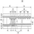
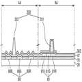
도 1은 본 발명의 일 실시예에 따른 표시 장치의 단면도이다. 도 1을 참조하면, 표시 장치(100)는 TN 모드의 액정 표시 장치로서, 제1 기판(10), 제2 기판(20), 공통 전압 라인(41), 컬럼 스페이서(50), 도전층(61), 공통 전극(62) 및 액정층(90)을 포함한다. 설명의 편의를 위하여 도 1은 표시 장치(100)의 일부 단면만을 도시하였다.1 is a cross-sectional view of a display device according to an embodiment of the present invention. 1, a
제1 기판(10) 및 제2 기판(20) 각각은 표시 장치(100)의 하부 및 상부에 위치하는 기판으로서, 절연 물질로 구성될 수 있고, 구체적으로 유리 또는 플라스틱으로 이루어질 수 있다.Each of the
제1 기판(10)과 제2 기판(20)은 서로 대향하도록 배치되고, 제1 기판(10)과 제2 기판(20) 사이에는 액정층(90)이 개재된다. 또한, 액정층(90)의 외곽, 즉, 제1 기판(10)과 제2 기판(20)의 외곽 영역에는 실런트(sealant; 95)가 배치될 수 있다. 실런트(95)는 제1 기판(10)과 제2 기판(20) 내부를 밀봉하여 내부 소자를 보호하기 위한 것으로서, 열경화성 물질 또는 광경화성 물질 등 다양한 물질로 구성될 수 있다.The
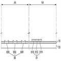
제1 기판(10) 및 제2 기판(20)은 각각 표시 영역(AA) 및 비표시 영역(NA)을 포함하고, 비표시 영역(NA)은 표시 영역(AA)을 둘러싸는 영역일 수 있다. 표시 영역(AA)은 표시 장치(100)에서 화상이 디스플레이되는 영역을 의미하고, 비표시 영역(NA)은 표시 장치(100)에서 표시 영역(AA)이 제외된 나머지 영역을 의미하는 것으로서, 비표시 영역(NA)에는 다양한 배선들이 배치되고, 실런트(95) 또한 비표시 영역(NA)에 배치될 수 있다. 제1 기판(10)의 표시 영역(AA)과 제2 기판(20)의 표시 영역(AA)은 서로 대응하는 영역이고, 제1 기판(10)의 비표시 영역(NA)과 제2 기판(20)의 비표시 영역(NA) 또한 서로 대응하는 영역일 수 있다.The
제1 기판(10) 상에는 하나 이상의 박막 트랜지스터(30)가 형성될 수 있고, 박막 트랜지스터(30)는 제1 기판(10)의 표시 영역(AA)에 형성될 수 있다. 도 1에서는 설명의 편의를 위해 박막 트랜지스터(30)를 하나의 엘리먼트로 도시하였으나, 박막 트랜지스터(30)는 게이트 전극, 반도체층, 소스 전극 및 드레인 전극을 포함할 수 있다. 박막 트랜지스터(30)의 구성은 앞서 설명한 예에 한정되지 않고, 당업자가 용이하게 실시할 수 있는 공지된 구성으로 다양하게 변형 가능하다. 이와 같이, 제1 기판(10)에 표시 장치(100)를 구동하기 위한 박막 트랜지스터(30)가 형성되는 경우, 제1 기판(10)은 박막 트랜지스터 기판이라고도 지칭될 수 있다.One or more
제1 기판(10)의 비표시 영역(NA)에는 다양한 배선들이 형성될 수 있다. 도 1을 참조하면, 제1 기판(10)의 비표시 영역(NA)에는 공통 전압 라인(41) 및 게이트 배선(43)이 형성된다. 공통 전압 라인(41)은 공통 전극(62)에 공통 전압을 인가하기 위한 배선이고, 게이트 배선(43)은 박막 트랜지스터(30)의 게이트 전극에 게이트 신호를 인가하기 위한 배선이다. 도 1에는 도시되지 않았으나, 공통 전압 라인(41) 및 게이트 배선(43)은 표시 영역(AA) 측으로 연결되어 신호를 전달할 수 있다.Various wirings may be formed in the non-display area NA of the
제1 기판(10) 상에는 공통 전압 라인(41)과 게이트 배선(43) 등과 같은 다양한 배선들을 커버하도록 절연막(44)이 형성될 수 있다. 절연막(44)은 제1 기판(10)의 표시 영역(AA)과 비표시 영역(NA) 모두에 형성될 수 있으며, 공통 전압 라인(41)의 일부 영역을 개구시킬 수 있다. 몇몇 실시예에서, 절연막(44)은 게이트 절연막일 수 있다.An
제1 기판(10) 상에는 공통 전압 라인(41) 상에 형성되고, 공통 전압 라인(41)과 전기적으로 연결되는 중간 도전체(42)가 형성될 수 있다. 중간 도전체(42)는 절연막(44) 상에 형성되고, 절연막(44)의 개구 영역을 통해 중간 도전체(42)와 전기적으로 연결될 수 있다. 몇몇 실시예에서, 중간 도전체(42)는 박막 트랜지스터(30)의 소스 전극 및 드레인 전극과 실질적으로 동일한 물질로 형성될 수 있고, 박막 트랜지스터(30)의 소스 전극 및 드레인 전극과 실질적으로 동시에 형성될 수 있다.An
제1 기판(10) 상에는 중간 도전체(42)를 커버하도록 패시베이션막(45)이 형성될 수 있다. 제1 기판(10)의 표시 영역(AA)과 비표시 영역(NA) 모두에 형성될 수 있으며, 중간 도전체(42)의 일부 영역을 개구시킬 수 있다.A
제1 기판(10) 상에는 박막 트랜지스터(30)를 보호하고, 개구율을 높이기 위한 유기막(46)이 형성될 수 있다. 유기막(46)은 제1 기판(10)의 표시 영역(AA)과 비표시 영역(NA) 모두에 형성될 수 있으며, 중간 도전체(42)의 일부 영역을 개구시킬 수 있고, 박막 트랜지스터(30)의 일부 영역을 개구시킬 수도 있다.On the
제1 기판(10)상에는 제1 기판(10)과 제2 기판(20) 사이의 셀갭을 유지하기 위해 하나 이상의 컬럼 스페이서(50)가 형성될 수 있다. 컬럼 스페이서(50)는 제1 기판(10) 상에서 비표시 영역(NA)에 형성되는 제1 컬럼 스페이서(51) 및 표시 영역(AA)에 형성되는 제2 컬럼 스페이서(52)를 포함할 수 있다. 제1 컬럼 스페이서(51)는 비표시 영역(NA)에서 공통 전압 라인(41) 상에 배치될 수 있고, 제2 컬럼 스페이서(52)는 표시 영역(AA)에서 유기막(46) 상에 배치될 수 있다. 비표시 영역(NA)에 형성되는 제1 컬럼 스페이서(51)는 비표시 영역(NA)에 형성되는 실런트(95)보다 표시 영역(AA)에 인접하게 배치될 수 있다. 도 1에서는 설명의 편의를 위해 제1 컬럼 스페이서(51)를 2개로 도시하고, 제2 컬럼 스페이서(52)를 1개로 도시하였으나, 이에 제한되지 않고, 다양한 개수로 설계되어 형성될 수 있다.One or
제1 기판(10) 상에는 비표시 영역(NA)에 형성되는 제1 컬럼 스페이서(51)를 커버하도록 형성되는 도전층(61)이 형성된다. 도전층(61)은 비표시 영역(NA)에 형성되는 제1 컬럼 스페이서(51)를 커버하도록 형성되어, 제1 컬럼 스페이서(51)의 표면을 따라 컨포멀(conformal)하게 형성될 수 있다. 도전층(61)은 투명한 전도성 물질로 형성될 수 있고, 예를 들어, IZO, IZO 등과 같은 투명 전도성 물질로 형성될 수 있다. 도전층(61)은 제1 기판(10)의 표시 영역(AA)에 형성될 수 있으며, 제1 기판(10)의 표시 영역(AA)에 형성되는 도전층(61)은 화소 전극으로 기능할 수 있다. 따라서, 제1 기판(10)의 표시 영역(AA)에 형성되는 도전층(61)은 유기막(46)의 개구부를 통해 박막 트랜지스터(30)의 드레인 전극과 전기적으로 연결될 수 있다. 또한, 도전층(61)은 제1 기판(10)의 비표시 영역(NA)에 형성될 수 있으며, 제1 기판(10)의 비표시 영역(NA)에 형성되는 도전층(61)은 패시베이션막(45) 및 유기막(46)의 개구부를 통해 공통 전압 라인(41)에 전기적으로 연결되고, 구체적으로, 중간 도전체(42)를 통해 공통 전압 라인(41)에 전기적으로 연결될 수 있다. 도전층(61)은 공통 전압 라인(41)과 전기적으로 연결되어 제2 기판(20)에 형성되는 공통 전극(62)에 공통 전압을 인가할 수 있으며, 이에 대해서는 후술한다.A
제2 기판(20) 상에는 소정의 패턴으로 블랙 매트릭스(70)가 형성될 수 있다. 블랙 매트릭스(70)는 제2 기판(20)의 표시 영역(AA) 및 비표시 영역(NA) 모두에 형성될 수 있고, 컬러 필터(80)를 통하여 구현되는 가시광선들의 혼색 및 간섭을 방지함과 동시에, 시인이 불필요한 구성의 시인을 저지하는 역할을 할 수 있다. 블랙 매트릭스(70)의 소정의 패턴은 개구부를 포함하는데, 컬러 필터(80)는 적색 컬러 필터(80), 녹색 컬러 필터(80) 및 청색 컬러 필터(80)를 포함할 수 있고, 블랙 매트릭스(70)의 개구부를 충진하는 방식으로 형성될 수 있다. 컬러 필터(80)는 블랙 매트릭스(70)를 충진하는 과정에서 일부가 블랙 매트릭스(70) 상에 형성될 수 있다. 도 1에서는 컬러 필터(80)의 일부가 블랙 매트릭스(70) 상에 형성되는 실시예를 도시하였으나, 컬러 필터(80)가 블랙 매트릭스(70) 상에 존재하지 않게 블랙 매트릭스(70)의 개구부를 충진할 수도 있음은 자명하다. 제2 기판(20)의 비표시 영역(NA)에는 더미 컬러 필터(81)가 형성될 수도 있고, 더미 컬러 필터(81)는 비표시 영역(NA)에 형성된 블랙 매트릭스(70) 상에 형성될 수도 있다. 이와 같이, 제2 기판(20)에 컬러 필터(80)가 형성되는 경우, 제2 기판(20)은 컬러 필터 기판이라고도 지칭될 수 있다.A
제2 기판(20) 상에는 블랙 매트릭스(70), 컬러 필터(80) 및 더미 컬러 필터(81)를 커버하도록 오버코팅층(47)이 형성될 수 있다. 오버코팅층(47)은 제2 기판(20)의 표시 영역(AA)과 비표시 영역(NA) 모두에 형성될 수 있다.An
제2 기판(20) 상에는 공통 전극(62)이 형성될 수 있다. 공통 전극(62)은 제2 기판(20)의 표시 영역(AA)과 비표시 영역(NA) 모두에 형성될 수 있고, 블랙 매트릭스(70), 컬러 필터(80) 및 더미 컬러 필터(81) 상에 형성될 수 있다. 또한, 공통 전극(62)은 오버코팅층(47) 상에 형성될 수 있다. 공통 전극(62)은 투명한 전도성 물질로 형성될 수 있고, 예를 들어, IZO, IZO 등과 같은 투명 전도성 물질로 형성될 수 있다.A
제2 기판(20) 상에 형성된 공통 전극(62)과 제1 기판(10) 상에 형성된 도전층(61)은 전기적으로 연결된다. 따라서, 공통 전압 라인(41)에 입력되는 공통 전압은 공통 전극(62)으로 인가될 수 있고, 구체적으로 공통 전압 라인(41)에 입력되는 공통 전압은 중간 도전체(42), 도전층(61)을 통해 공통 전극(62)으로 입력될 수 있다.The
본 발명의 일 실시예에 따른 표시 장치에서는 공통 전압 라인과 공통 전극을 쇼트시키기 위한 쇼트 포인트가 불필요하다. 즉, 종래에는 박막 트랜지스터 기판에 배치되는 공통 전압 라인과, 컬러 필터 기판에 배치되는 공통 전극을 전기적으로 연결하기 위해, 비표시 영역에 별도의 쇼트 포인트를 형성하였으며, 이에, 비표시 영역의 폭이 증가하였으며, 이에 따라 블랙 매트릭스의 폭 또한 증가하였다. 그러나, 본 발명의 일 실시예에 따른 표시 장치에서는 별도의 쇼트 포인트 제조 없이 컬럼 스페이서가 쇼트 포인트 역할을 대신할 수 있으므로, 공정 단순화가 가능하다. 또한, 본 발명의 일 실시예에 따른 표시 장치에서는 쇼트 포인트를 형성하기 위한 별도의 영역을 비표시 영역 상에 확보할 필요가 없으므로, 블랙 매트릭스의 폭을 작게 형성하는 슬림 BM 구조 적용이 가능하다.The display device according to the embodiment of the present invention does not need a short point for shorting the common voltage line and the common electrode. That is, conventionally, in order to electrically connect the common voltage line arranged on the thin film transistor substrate and the common electrode arranged on the color filter substrate, a separate short point is formed in the non-display area, And thus the width of the black matrix also increased. However, in the display device according to the embodiment of the present invention, since the column spacer can take the role of a short point without preparing another short point, the process can be simplified. Further, in the display device according to the embodiment of the present invention, it is not necessary to secure a separate area for forming the short point on the non-display area, so that the slim BM structure in which the width of the black matrix is small can be applied.
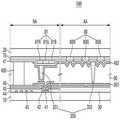
도 2는 본 발명의 다른 실시예에 따른 표시 장치의 단면도이다. 도 2를 참조하면, 표시 장치(200)는 VA 모드의 액정 표시 장치로서, 제1 기판(10), 제2 기판(20), 공통 전압 라인(41), 컬럼 스페이서(50), 도전층(16), 공통 전극(162) 및 액정층(90)을 포함한다. 설명의 편의를 위하여 도 2는 표시 장치(200)의 일부 단면만을 도시하였다. 설명의 편의 상, 도 1에 도시된 표시 장치의 도면에 나타낸 각 엘리먼트와 실질적으로 동일한 엘리먼트는 동일 부호로 나타내고, 중복 설명을 생략한다.2 is a cross-sectional view of a display device according to another embodiment of the present invention. 2, the
제2 기판(20) 상에는 공통 전극(162)이 형성될 수 있다. 공통 전극(162)은 제2 기판(20)의 표시 영역(AA)과 비표시 영역(NA) 모두에 형성될 수 있고, 블랙 매트릭스(70), 컬러 필터(80) 및 더미 컬러 필터(81) 상에 형성될 수 있다. 또한, 공통 전극(162)은 오버코팅층(47) 상에 형성될 수 있다. 공통 전극(162)은 컬러 필터(80)의 일부 영역을 개구시키는 절개부를 포함할 수 있고, 실런트(195)와 서로 중첩하지 않을 수 있다. 공통 전극(162)이 절개부를 포함하고, 실런트(195)와 중첩하지 않는다는 것을 제외하면, 공통 전극(162) 및 실런트(195)는 도 1의 공통 전극 및 실런트와 실질적으로 동일하므로, 중복 설명을 생략한다.A
도 3은 본 발명의 다른 실시예에 따른 표시 장치의 단면도이다. 도 3을 참조하면, 표시 장치(300)는 박리 개선형 TN 모드의 액정 표시 장치로서, 제1 기판(10), 제2 기판(20), 공통 전압 라인(41), 컬럼 스페이서(50), 도전층(61), 공통 전극(262) 및 액정층(90)을 포함한다. 설명의 편의를 위하여 도 3은 표시 장치(300)의 일부 단면만을 도시하였다. 설명의 편의 상, 도 1에 도시된 표시 장치의 도면에 나타낸 각 엘리먼트와 실질적으로 동일한 엘리먼트는 동일 부호로 나타내고, 중복 설명을 생략한다.3 is a cross-sectional view of a display device according to another embodiment of the present invention. 3, the
제2 기판(20) 상에는 공통 전극(262)이 형성될 수 있다. 공통 전극(262)은 제2 기판(20)의 표시 영역(AA)과 비표시 영역(NA) 모두에 형성될 수 있고, 블랙 매트릭스(70), 컬러 필터(80) 및 더미 컬러 필터(81) 상에 형성될 수 있다. 또한, 공통 전극(262)은 오버코팅층(47) 상에 형성될 수 있다. 공통 전극(262)은 실런트(295)와 서로 중첩하지 않을 수 있다. 공통 전극(262)이 실런트(295)와 중첩하지 않는다는 것을 제외하면, 공통 전극(262) 및 실런트(295)는 도 1의 공통 전극 및 실런트와 실질적으로 동일하므로, 중복 설명을 생략한다.A
TN 모드에서 실런트 아래 부분에 공통 전극이 있는 경우, 박리 불량에 취약할 수 있다. 이에, 본 발명의 다른 실시예에 따른 표시 장치에서는 VA 모드와 같이 TN 모드에서도 실런트 아래 부분에 공통 전극을 제거할 수 있고, 박리 불량 문제를 해결할 수 있다.If there is a common electrode under the sealant in the TN mode, it may be vulnerable to peeling failure. Thus, in the display device according to another embodiment of the present invention, the common electrode can be removed at the lower portion of the sealant even in the TN mode such as the VA mode, and the problem of peeling failure can be solved.
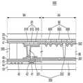
도 4는 본 발명의 다른 실시예에 따른 표시 장치의 단면도이다. 도 4를 참조하면, 표시 장치(400)는 TN 모드의 액정 표시 장치로서, 제1 기판(10), 제2 기판(20), 공통 전압 라인(41), 컬럼 스페이서(350), 도전층(361), 공통 전극(362) 및 액정층(90)을 포함한다. 설명의 편의를 위하여 도 4는 표시 장치(400)의 일부 단면만을 도시하였다. 설명의 편의 상, 도 1에 도시된 표시 장치의 도면에 나타낸 각 엘리먼트와 실질적으로 동일한 엘리먼트는 동일 부호로 나타내고, 중복 설명을 생략한다.4 is a cross-sectional view of a display device according to another embodiment of the present invention. 4, the display device 400 includes a
제1 기판(10) 상에는 도전층(361)이 형성된다. 도전층(361)은 투명한 전도성 물질로 형성될 수 있고, 예를 들어, IZO, IZO 등과 같은 투명 전도성 물질로 형성될 수 있다. 도전층(361)은 제1 기판(10)의 표시 영역(AA)에 형성될 수 있으며, 제1 기판(10)의 표시 영역(AA)에 형성되는 도전층(361)은 화소 전극으로 기능할 수 있다. 따라서, 제1 기판(10)의 표시 영역(AA)에 형성되는 도전층(361)은 유기막(46)의 개구부를 통해 박막 트랜지스터(30)의 드레인 전극과 전기적으로 연결될 수 있다. 또한, 도전층(361)은 제1 기판(10)의 비표시 영역(NA)에 형성될 수 있으며, 제1 기판(10)의 비표시 영역(NA)에 형성되는 도전층(361)은 패시베이션막(45) 및 유기막(46)의 개구부를 통해 공통 전압 라인(41)에 전기적으로 연결되고, 구체적으로, 중간 도전체(42)를 통해 공통 전압 라인(41)에 전기적으로 연결될 수 있다. 도전층(361)은 공통 전압 라인(41)과 전기적으로 연결되어 제2 기판(20)에 형성되는 공통 전극(362)에 공통 전압을 인가할 수 있으며, 이에 대해서는 후술한다.On the
제2 기판(20)상에는 제1 기판(10)과 제2 기판(20) 사이의 셀갭을 유지하기 위해 하나 이상의 컬럼 스페이서(350)가 형성될 수 있다. 컬럼 스페이서(350)는 제2 기판(20) 상에서 비표시 영역(NA)에 형성되는 제1 컬럼 스페이서(351) 및 표시 영역(AA)에 형성되는 제2 컬럼 스페이서(352)를 포함할 수 있다. 제1 컬럼 스페이서3(51)는 비표시 영역(NA)에서 오버코팅층(47) 상에 배치될 수 있고, 제2 컬럼 스페이서(352)는 표시 영역(AA)에서 오버코팅층(47) 상에 배치될 수 있다. 비표시 영역(NA)에 형성되는 제1 컬럼 스페이서(351)는 비표시 영역(NA)에 형성되는 실런트(395)보다 표시 영역(AA)에 인접하게 배치될 수 있다. 도 4에서는 설명의 편의를 위해 제1 컬럼 스페이서(351)를 1개로 도시하고, 제2 컬럼 스페이서(352)를 1개로 도시하였으나, 이에 제한되지 않고, 다양한 개수로 설계되어 형성될 수 있다.One or
제2 기판(20) 상에는 공통 전극(362)이 형성될 수 있다. 공통 전극(362)은 제2 기판(20)의 표시 영역(AA)과 비표시 영역(NA) 모두에 형성될 수 있고, 블랙 매트릭스(70), 컬러 필터(80) 및 더미 컬러 필터(81) 상에 형성될 수 있다. 또한, 공통 전극(362)은 오버코팅층(47) 상에서 비표시 영역(NA)에 형성되는 제1 컬럼 스페이서(51)를 커버하도록 형성될 수 있으며, 제1 컬럼 스페이서(351)의 표면을 따라 컨포멀하게 형성될 수 있다.A
제2 기판(20) 상에 형성된 공통 전극(362)과 제1 기판(10) 상에 형성된 도전층(361)은 전기적으로 연결된다. 따라서, 공통 전압 라인(41)에 입력되는 공통 전압은 공통 전극(362)으로 인가될 수 있고, 구체적으로 공통 전압 라인(41)에 입력되는 공통 전압은 중간 도전체(42), 도전층(361)을 통해 공통 전극(362)으로 입력될 수 있다.The
본 발명의 다른 실시예에 따른 표시 장치에서는 공통 전압 라인과 공통 전극을 쇼트시키기 위한 쇼트 포인트가 불필요하다. 즉, 종래에는 박막 트랜지스터 기판에 배치되는 공통 전압 라인과, 컬러 필터 기판에 배치되는 공통 전극을 전기적으로 연결하기 위해, 비표시 영역에 별도의 쇼트 포인트를 형성하였으며, 이에, 비표시 영역의 폭이 증가하였으며, 이에 따라 블랙 매트릭스의 폭 또한 증가하였다. 그러나, 본 발명의 다른 실시예에 따른 표시 장치에서는 별도의 쇼트 포인트 제조 없이 컬럼 스페이서가 쇼트 포인트 역할을 대신할 수 있으므로, 공정 단순화가 가능하다. 또한, 본 발명의 다른 실시예에 따른 표시 장치에서는 쇼트 포인트를 형성하기 위한 별도의 영역을 비표시 영역 상에 확보할 필요가 없으므로, 블랙 매트릭스의 폭을 작게 형성하는 슬림 BM 구조 적용이 가능하다.The display device according to another embodiment of the present invention does not need a short point for shorting the common voltage line and the common electrode. That is, conventionally, in order to electrically connect the common voltage line arranged on the thin film transistor substrate and the common electrode arranged on the color filter substrate, a separate short point is formed in the non-display area, And thus the width of the black matrix also increased. However, in the display device according to another embodiment of the present invention, since the column spacer can take the role of a short point without preparing another short point, the process can be simplified. Further, in the display device according to another embodiment of the present invention, it is not necessary to secure a separate area for forming a short point on the non-display area, so that the slim BM structure in which the width of the black matrix is small can be applied.
도 5는 본 발명의 다른 실시예에 따른 표시 장치의 단면도이다. 도 2를 참조하면, 표시 장치(500)는 VA 모드의 액정 표시 장치로서, 제1 기판(10), 제2 기판(20), 공통 전압 라인(41), 컬럼 스페이서(350), 도전층(361), 공통 전극(462) 및 액정층(90)을 포함한다. 설명의 편의를 위하여 도 5는 표시 장치(500)의 일부 단면만을 도시하였다. 설명의 편의 상, 도 4에 도시된 표시 장치의 도면에 나타낸 각 엘리먼트와 실질적으로 동일한 엘리먼트는 동일 부호로 나타내고, 중복 설명을 생략한다.5 is a cross-sectional view of a display device according to another embodiment of the present invention. 2, the
제2 기판(20) 상에는 공통 전극(462)이 형성될 수 있다. 공통 전극(462)은 제2 기판(20)의 표시 영역(AA)과 비표시 영역(NA) 모두에 형성될 수 있고, 블랙 매트릭스(70), 컬러 필터(80), 더미 컬러 필터(81) 및 컬럼 스페이서(350) 상에 형성될 수 있다. 또한, 공통 전극(462)은 오버코팅층(47) 상에 형성될 수 있다. 공통 전극(462)은 컬러 필터(80)의 일부 영역을 개구시키는 절개부를 포함할 수 있고, 실런트(495)와 서로 중첩하지 않을 수 있다. 공통 전극(462)이 절개부를 포함하고, 실런트(495)와 중첩하지 않는다는 것을 제외하면, 공통 전극(462) 및 실런트(495)는 도 4의 공통 전극 및 실런트와 실질적으로 동일하므로, 중복 설명을 생략한다.A
도 6은 본 발명의 다른 실시예에 따른 표시 장치의 단면도이다. 도 6을 참조하면, 표시 장치(600)는 박리 개선형 TN 모드의 액정 표시 장치로서, 제1 기판(10), 제2 기판(20), 공통 전압 라인(41), 컬럼 스페이서(350), 도전층(361), 공통 전극(562) 및 액정층(90)을 포함한다. 설명의 편의를 위하여 도 6은 표시 장치(600)의 일부 단면만을 도시하였다. 설명의 편의 상, 도 4에 도시된 표시 장치의 도면에 나타낸 각 엘리먼트와 실질적으로 동일한 엘리먼트는 동일 부호로 나타내고, 중복 설명을 생략한다.6 is a cross-sectional view of a display device according to another embodiment of the present invention. Referring to FIG. 6, the
제2 기판(20) 상에는 공통 전극(562)이 형성될 수 있다. 공통 전극(562)은 제2 기판(20)의 표시 영역(AA)과 비표시 영역(NA) 모두에 형성될 수 있고, 블랙 매트릭스(70), 컬러 필터(80), 더미 컬러 필터(81) 및 컬럼 스페이서(350) 상에 형성될 수 있다. 또한, 공통 전극(562)은 오버코팅층(47) 상에 형성될 수 있다. 공통 전극(562)은 실런트(595)와 서로 중첩하지 않을 수 있다. 공통 전극(562)이 실런트(595)와 중첩하지 않는다는 것을 제외하면, 공통 전극(562) 및 실런트(595)는 도 4의 공통 전극 및 실런트와 실질적으로 동일하므로, 중복 설명을 생략한다.A
TN 모드에서 실런트 아래 부분에 공통 전극이 있는 경우, 박리 불량에 취약할 수 있다. 이에, 본 발명의 다른 실시예에 따른 표시 장치에서는 VA 모드와 같이 TN 모드에서도 실런트 아래 부분에 공통 전극을 제거할 수 있고, 박리 불량 문제를 해결할 수 있다.If there is a common electrode under the sealant in the TN mode, it may be vulnerable to peeling failure. Thus, in the display device according to another embodiment of the present invention, the common electrode can be removed at the lower portion of the sealant even in the TN mode such as the VA mode, and the problem of peeling failure can be solved.
도 7은 본 발명의 일 실시예에 따른 표시 장치 제조 방법의 순서도이다. 도 8 내지 도 12는 본 발명의 일 실시예에 따른 표시 장치 제조 방법을 설명하기 위한 공정별 단면도들이다.7 is a flowchart of a method of manufacturing a display device according to an embodiment of the present invention. 8 to 12 are cross-sectional views for explaining a method of manufacturing a display device according to an embodiment of the present invention.
먼저, 기판(20) 상에 블랙 매트릭스(70) 및 컬러 필터(80)를 형성한다(S70). 기판(20) 상에 블랙 매트릭스(70) 및 컬러 필터(80)를 형성하는 것은 도 1 내지 도 6의 기판 상에 블랙 매트릭스 및 컬러 필터를 형성하는 것과 실질적으로 동일하므로 중복 설명을 생략한다.First, a
컬리 필터(80)를 형성하는 것은 비표시 영역(NA)에 형성된 블랙 매트릭스(70) 상에 더미 컬러 필터(81)를 형성하는 것을 포함할 수 있다. 더미 컬러 필터(81)를 형성하는 것은 도 1 내지 도 6의 더미 컬러 필터를 형성하는 것과 실질적으로 동일하므로 중복 설명을 생략한다.Forming the
이어서, 블랙 매트릭스(70) 및 컬러 필터(80) 상에 오버코팅층(47)을 형성한다(S71). 오버코팅층(47)을 형성하는 것은 도 1 내지 도 6의 오버코팅층을 형성하는 것과 실질적으로 동일하므로 중복 설명을 생략한다.Then, an
이어서, 오버코팅층(47) 상에 제1 컬럼 스페이서(351) 및 제2 컬럼 스페이서(352)를 형성한다(S72). 제1 컬럼 스페이서(351) 및 제2 컬럼 스페이서(352)를 형성하는 것은 도 4 내지 도 6의 제1 컬럼 스페이서 및 제2 컬럼 스페이서를 형성하는 것과 실질적으로 동일하므로 중복 설명을 생략한다.Next, a
이어서, 오버코팅층(47) 및 제1 컬럼 스페이서(351) 상에 공통 전극(462)을 형성한다(S73). 공통 전극(462)을 형성하는 것은 도 5의 공통 전극을 형성하는 것과 실질적으로 동일하므로 중복 설명을 생략한다.Next, a
이상 첨부된 도면을 참조하여 본 발명의 실시예들을 설명하였지만, 본 발명이 속하는 기술분야에서 통상의 지식을 가진 자는 본 발명의 그 기술적 사상이나 필수적인 특징을 변경하지 않고서 다른 구체적인 형태로 실시될 수 있다는 것을 이해할 수 있을 것이다. 그러므로 이상에서 기술한 실시예들은 모든 면에서 예시적인 것이며 한정적이 아닌 것으로 이해해야만 한다.While the present invention has been described in connection with what is presently considered to be practical exemplary embodiments, it is to be understood that the invention is not limited to the disclosed embodiments, but, on the contrary, You will understand. It is therefore to be understood that the above-described embodiments are illustrative in all aspects and not restrictive.
10: 제1 기판
20: 제2 기판
30: 박막 트랜지스터
41: 공통 전압 라인
42: 중간 도전체
43: 게이트 배선
44: 절연막
45: 패시베이션막
46: 유기막
47: 오버코팅층
50, 350: 컬럼 스페이서
51, 351: 제1 컬럼 스페이서
52, 352: 제2 컬럼 스페이서
61, 361: 도전층
62, 162, 262, 362, 462, 562: 공통 전극
70: 블랙 매트릭스
80: 컬러 필터
81: 더미 컬러 필터
90: 액정층
95, 195, 295, 395, 495, 595: 실런트
100, 200, 300, 400, 500, 600: 표시 장치
AA: 표시 영역
NA: 비표시 영역10: first substrate
20: second substrate
30: Thin film transistor
41: common voltage line
42: intermediate conductor
43: gate wiring
44: Insulating film
45: Passivation film
46: organic film
47: overcoat layer
50, 350: Column spacer
51, 351: first column spacer
52, 352: second column spacer
61, 361: conductive layer
62, 162, 262, 362, 462, 562:
70: Black Matrix
80: Color filter
81: Dummy color filter
90: liquid crystal layer
95, 195, 295, 395, 495, 595: sealant
100, 200, 300, 400, 500, 600: display device
AA: display area
NA: non-display area
Claims (25)
Translated fromKorean상기 제1 기판 상의 상기 비표시 영역에 형성되는 공통 전압 라인;
상기 제1 기판 상의 상기 표시 영역과 상기 비표시 영역에 형성되는 유기막;
상기 유기막 상의 상기 비표시 영역에 형성되는 하나 이상의 컬럼 스페이서;
상기 유기막 상에 형성되고, 상기 유기막의 개구부를 통해 상기 공통 전압 라인과 전기적으로 연결되는 도전층;
상기 제2 기판 하부에 형성되고, 상기 도전층과 전기적으로 연결되는 공통 전극;
상기 제1 기판과 상기 제2 기판 사이에 개재되는 액정층; 및
상기 제1 기판과 상기 제2 기판 사이에 배치되는 실런트를 포함하되,
상기 컬럼 스페이서는 상기 제1 기판과 대향하는 저면과 상기 제2 기판과 대향하는 상면을 포함하고,
상기 컬럼 스페이서의 상기 저면은 상기 유기막과 접하고,
상기 도전층은 상기 하나 이상의 컬럼 스페이서의 상기 상면에서 상기 공통 전극과 전기적으로 연결되도록 상기 컬럼 스페이서 상으로 연장되는 표시 장치.A first substrate and a second substrate facing each other and including a display region and a non-display region surrounding the display region;
A common voltage line formed in the non-display region on the first substrate;
An organic film formed on the display region and the non-display region on the first substrate;
At least one column spacer formed in the non-display area on the organic film;
A conductive layer formed on the organic layer and electrically connected to the common voltage line through an opening of the organic layer;
A common electrode formed under the second substrate and electrically connected to the conductive layer;
A liquid crystal layer interposed between the first substrate and the second substrate; And
And a sealant disposed between the first substrate and the second substrate,
Wherein the column spacer includes a bottom surface facing the first substrate and an upper surface facing the second substrate,
The bottom surface of the column spacer being in contact with the organic film,
Wherein the conductive layer extends on the column spacer so as to be electrically connected to the common electrode at the top surface of the at least one column spacer.
상기 제1 기판 상에 형성되는 하나 이상의 박막 트랜지스터를 더 포함하되,
상기 박막 트랜지스터는 게이트 전극, 소스 전극, 드레인 전극 및 반도체층을 포함하는 표시 장치.The method according to claim 1,
Further comprising at least one thin film transistor formed on the first substrate,
Wherein the thin film transistor includes a gate electrode, a source electrode, a drain electrode, and a semiconductor layer.
상기 공통 전압 라인 상에 형성되고, 상기 공통 전압 라인과 전기적으로 연결되는 중간 도전체를 더 포함하고,
상기 도전층은 상기 중간 도전체를 통해 상기 공통 전압 라인과 전기적으로 연결되는 표시 장치.3. The method of claim 2,
Further comprising an intermediate conductor formed on the common voltage line and electrically connected to the common voltage line,
And the conductive layer is electrically connected to the common voltage line through the intermediate conductor.
상기 중간 도전체는 상기 소스 전극 및 상기 드레인 전극과 동일한 물질로 형성되는 표시 장치.The method of claim 3,
Wherein the intermediate conductor is formed of the same material as the source electrode and the drain electrode.
상기 드레인 전극과 전기적으로 연결되는 화소 전극을 더 포함하되,
상기 도전층은 상기 화소 전극과 동일한 물질로 형성되는 표시 장치.3. The method of claim 2,
And a pixel electrode electrically connected to the drain electrode,
Wherein the conductive layer is formed of the same material as the pixel electrode.
상기 컬럼 스페이서는 상기 비표시 영역에서 상기 실런트보다 상기 표시 영역에 인접하게 배치되고,
상기 도전층과 상기 공통 전극은 상기 실런트와 중첩되지 않는 표시 장치.The method according to claim 1,
Wherein the column spacer is disposed adjacent to the display area in the non-display area with respect to the sealant,
Wherein the conductive layer and the common electrode do not overlap with the sealant.
상기 제2 기판 상에 형성되는 컬러 필터 및 블랙 매트릭스를 더 포함하되,
상기 공통 전극은 상기 컬러 필터 및 상기 블랙 매트릭스 상에 형성되는 표시 장치.The method according to claim 1,
Further comprising a color filter and a black matrix formed on the second substrate,
And the common electrode is formed on the color filter and the black matrix.
상기 비표시 영역에 배치되는 상기 블랙 매트릭스 상에 형성되는 더미 컬러 필터를 더 포함하되,
상기 공통 전극은 상기 더미 컬러 필터 상에 형성되는 표시 장치.9. The method of claim 8,
And a dummy color filter formed on the black matrix disposed in the non-display area,
Wherein the common electrode is formed on the dummy color filter.
상기 공통 전극은 상기 컬러 필터의 일부 영역을 개구시키는 절개부를 포함하는 표시 장치.9. The method of claim 8,
And the common electrode includes a cutout portion that opens a part of the color filter.
Priority Applications (2)
| Application Number | Priority Date | Filing Date | Title |
|---|---|---|---|
| KR1020120080004AKR101985481B1 (en) | 2012-07-23 | 2012-07-23 | Display device and method of manufacturing the same |
| US13/834,895US9568775B2 (en) | 2012-07-23 | 2013-03-15 | Display device and method of manufacturing the same |
Applications Claiming Priority (1)
| Application Number | Priority Date | Filing Date | Title |
|---|---|---|---|
| KR1020120080004AKR101985481B1 (en) | 2012-07-23 | 2012-07-23 | Display device and method of manufacturing the same |
Publications (2)
| Publication Number | Publication Date |
|---|---|
| KR20140013325A KR20140013325A (en) | 2014-02-05 |
| KR101985481B1true KR101985481B1 (en) | 2019-06-05 |
Family
ID=49946265
Family Applications (1)
| Application Number | Title | Priority Date | Filing Date |
|---|---|---|---|
| KR1020120080004AActiveKR101985481B1 (en) | 2012-07-23 | 2012-07-23 | Display device and method of manufacturing the same |
Country Status (2)
| Country | Link |
|---|---|
| US (1) | US9568775B2 (en) |
| KR (1) | KR101985481B1 (en) |
Cited By (1)
| Publication number | Priority date | Publication date | Assignee | Title |
|---|---|---|---|---|
| US11751420B2 (en) | 2020-06-22 | 2023-09-05 | Samsung Display Co., Ltd. | Display device capable of facilitating substrate bonding with alignment key and method of fabricating the same |
Families Citing this family (39)
| Publication number | Priority date | Publication date | Assignee | Title |
|---|---|---|---|---|
| KR102240894B1 (en)* | 2014-02-26 | 2021-04-16 | 삼성디스플레이 주식회사 | Display device and method of manufacturing a display device |
| CN104062816A (en)* | 2014-06-09 | 2014-09-24 | 深圳市华星光电技术有限公司 | Liquid crystal panel and display device |
| JP6440486B2 (en)* | 2014-12-19 | 2018-12-19 | 株式会社ジャパンディスプレイ | LCD panel |
| KR102226397B1 (en)* | 2014-12-26 | 2021-03-11 | 엘지디스플레이 주식회사 | Liquid Crystal Display Device |
| KR102354969B1 (en)* | 2015-02-05 | 2022-01-25 | 삼성디스플레이 주식회사 | Organic light emitting display apparatus |
| KR102387683B1 (en)* | 2015-05-18 | 2022-04-19 | 삼성디스플레이 주식회사 | Liquid crystal display device |
| JP2016224299A (en)* | 2015-06-01 | 2016-12-28 | 株式会社ジャパンディスプレイ | Liquid crystal display device and three-dimensional image display device |
| CN105068294B (en)* | 2015-08-25 | 2018-01-12 | 深圳市华星光电技术有限公司 | A kind of liquid crystal display panel and device |
| KR102439841B1 (en)* | 2015-08-31 | 2022-09-01 | 엘지디스플레이 주식회사 | liquid crystal display |
| KR20170130660A (en)* | 2016-05-18 | 2017-11-29 | 삼성디스플레이 주식회사 | Display device |
| KR102526508B1 (en)* | 2016-06-30 | 2023-04-26 | 티씨엘 차이나 스타 옵토일렉트로닉스 테크놀로지 컴퍼니 리미티드 | Liquid display device |
| JP2018018006A (en)* | 2016-07-29 | 2018-02-01 | 株式会社ジャパンディスプレイ | Display device |
| JP2018017988A (en)* | 2016-07-29 | 2018-02-01 | 株式会社ジャパンディスプレイ | Display device |
| JP2018017978A (en)* | 2016-07-29 | 2018-02-01 | 株式会社ジャパンディスプレイ | Display device |
| JP2018017985A (en)* | 2016-07-29 | 2018-02-01 | 株式会社ジャパンディスプレイ | Display device and inter-substrate conduction structure |
| WO2018037988A1 (en)* | 2016-08-23 | 2018-03-01 | シャープ株式会社 | Display device |
| KR102415529B1 (en)* | 2017-06-12 | 2022-07-04 | 삼성디스플레이 주식회사 | Display apparatus |
| CN107167974A (en)* | 2017-07-07 | 2017-09-15 | 惠科股份有限公司 | Array substrate, manufacturing method thereof and display panel applied to array substrate |
| US10394093B2 (en) | 2017-07-07 | 2019-08-27 | HKC Corporation Limited | Array substrate, manufacturing method thereof, and applied display panel thereof |
| CN107589573A (en)* | 2017-08-25 | 2018-01-16 | 惠科股份有限公司 | Liquid crystal display panel and liquid crystal display device |
| KR102482967B1 (en)* | 2017-11-29 | 2022-12-28 | 엘지디스플레이 주식회사 | Display device |
| CN108107635A (en)* | 2017-12-21 | 2018-06-01 | 惠科股份有限公司 | Display, display panel thereof and manufacturing method of display |
| CN107966862B (en)* | 2017-12-21 | 2020-09-29 | 惠科股份有限公司 | Display, display panel thereof and manufacturing method of display |
| KR102477605B1 (en)* | 2018-01-23 | 2022-12-14 | 삼성디스플레이 주식회사 | Display apparatus and method of manufacturing the same |
| KR102562901B1 (en)* | 2018-03-26 | 2023-08-04 | 삼성디스플레이 주식회사 | Display apparatus |
| CN108919557A (en)* | 2018-08-31 | 2018-11-30 | 深圳市华星光电技术有限公司 | The production method of colored optical filtering substrates |
| CN208999729U (en)* | 2018-09-12 | 2019-06-18 | 重庆惠科金渝光电科技有限公司 | Display panel and display device |
| US10890808B2 (en)* | 2018-09-30 | 2021-01-12 | HKC Corporation Limited | Cell assembly, display panel and display device |
| CN110221474A (en)* | 2019-05-24 | 2019-09-10 | 深圳市华星光电技术有限公司 | Color membrane substrates and preparation method thereof |
| EP4020076A4 (en) | 2019-08-20 | 2022-08-03 | BOE Technology Group Co., Ltd. | DISPLAY PANEL AND DISPLAY DEVICE |
| CN111103735A (en)* | 2020-01-10 | 2020-05-05 | Oppo广东移动通信有限公司 | Horizontal electric field type display panel, electronic equipment |
| CN111240117B (en)* | 2020-03-25 | 2022-07-12 | 深圳市华星光电半导体显示技术有限公司 | Display panel and display device |
| CN111983855A (en) | 2020-08-10 | 2020-11-24 | 深圳市华星光电半导体显示技术有限公司 | Display panel and display device |
| CN114442387B (en)* | 2020-10-30 | 2025-04-22 | 京东方科技集团股份有限公司 | Array substrate and manufacturing method thereof, and display device |
| JP7561672B2 (en) | 2021-03-31 | 2024-10-04 | 株式会社ジャパンディスプレイ | Display device |
| CN113138488A (en)* | 2021-04-13 | 2021-07-20 | 深圳市华星光电半导体显示技术有限公司 | Display panel |
| CN114035362B (en)* | 2021-11-15 | 2023-10-13 | 惠州华星光电显示有限公司 | Liquid crystal display panel and display device |
| CN115079478B (en)* | 2022-06-30 | 2023-11-10 | 厦门天马微电子有限公司 | Display panel and display device |
| CN115224094A (en)* | 2022-07-25 | 2022-10-21 | 昆山国显光电有限公司 | A display panel and display device |
Citations (1)
| Publication number | Priority date | Publication date | Assignee | Title |
|---|---|---|---|---|
| US20070058125A1 (en)* | 2003-05-15 | 2007-03-15 | Young-Hoon Yoo | Liquid crystal display apparatus and method of forming the same |
Family Cites Families (9)
| Publication number | Priority date | Publication date | Assignee | Title |
|---|---|---|---|---|
| JP3014291B2 (en)* | 1995-03-10 | 2000-02-28 | インターナショナル・ビジネス・マシーンズ・コーポレイション | Liquid crystal display panel, liquid crystal display device, and method of manufacturing liquid crystal display panel |
| JP4094759B2 (en)* | 1999-02-05 | 2008-06-04 | 株式会社日立製作所 | Liquid crystal display |
| JP2001100217A (en)* | 1999-09-29 | 2001-04-13 | Nec Corp | Color liquid crystal display device and method for manufacturing the same |
| JP4884586B2 (en)* | 2000-12-18 | 2012-02-29 | 株式会社 日立ディスプレイズ | Liquid crystal display |
| JP2004212955A (en)* | 2002-12-16 | 2004-07-29 | Sharp Corp | Liquid crystal display |
| KR100964797B1 (en)* | 2003-12-23 | 2010-06-21 | 엘지디스플레이 주식회사 | Liquid Crystal Display and Manufacturing Method Thereof |
| JP2005258410A (en)* | 2004-03-08 | 2005-09-22 | Samsung Electronics Co Ltd | Liquid crystal display device and manufacturing method thereof |
| KR20070001659A (en)* | 2005-06-29 | 2007-01-04 | 엘지.필립스 엘시디 주식회사 | Liquid Crystal Display and Manufacturing Method Thereof |
| KR20070074891A (en)* | 2006-01-11 | 2007-07-18 | 삼성전자주식회사 | Color filter substrate and liquid crystal display panel including the same |
- 2012
- 2012-07-23KRKR1020120080004Apatent/KR101985481B1/enactiveActive
- 2013
- 2013-03-15USUS13/834,895patent/US9568775B2/enactiveActive
Patent Citations (1)
| Publication number | Priority date | Publication date | Assignee | Title |
|---|---|---|---|---|
| US20070058125A1 (en)* | 2003-05-15 | 2007-03-15 | Young-Hoon Yoo | Liquid crystal display apparatus and method of forming the same |
Cited By (2)
| Publication number | Priority date | Publication date | Assignee | Title |
|---|---|---|---|---|
| US11751420B2 (en) | 2020-06-22 | 2023-09-05 | Samsung Display Co., Ltd. | Display device capable of facilitating substrate bonding with alignment key and method of fabricating the same |
| US12178068B2 (en) | 2020-06-22 | 2024-12-24 | Samsung Display Co., Ltd. | Method of fabricating display device capable of facilitating substrate bonding with alignment key |
Also Published As
| Publication number | Publication date |
|---|---|
| KR20140013325A (en) | 2014-02-05 |
| US20140022478A1 (en) | 2014-01-23 |
| US9568775B2 (en) | 2017-02-14 |
Similar Documents
| Publication | Publication Date | Title |
|---|---|---|
| KR101985481B1 (en) | Display device and method of manufacturing the same | |
| KR101335276B1 (en) | Array substrat, display panel having the same and fabricating of display panel | |
| US10488698B2 (en) | Liquid crystal display device | |
| JP5717326B2 (en) | Liquid crystal device, electronic device, and method for manufacturing liquid crystal device | |
| CN102854665B (en) | Display devices and electronic equipment | |
| CN104749841B (en) | Thin-film transistor array base-plate and its manufacture method | |
| US8704990B2 (en) | Electro-optical display apparatus | |
| US9081234B2 (en) | Liquid crystal panel | |
| US9036103B2 (en) | Display substrate, method of manufacturing the same and display apparatus having the same | |
| US8143622B2 (en) | Display panel | |
| KR20090076812A (en) | Liquid crystal display device and liquid crystal display device manufacturing method | |
| CN106449652B (en) | Array substrate and its manufacturing method, display panel and display equipment | |
| US20110292331A1 (en) | Pixel structure and display panel having the same | |
| WO2012090788A1 (en) | Display element | |
| KR101936368B1 (en) | Display device and method of fabricating the same | |
| KR20120004194A (en) | Liquid crystal display panel and its manufacturing method | |
| JP5213616B2 (en) | Liquid crystal device, method for manufacturing liquid crystal device, and electronic apparatus | |
| KR102178887B1 (en) | Array substrate and liquid crystal display device inluding the same | |
| KR102016567B1 (en) | Flat panel display including thin film transistor substrate having color filter layer and manufacturing the same | |
| KR102004956B1 (en) | Display device | |
| US8477269B2 (en) | Liquid crystal display device | |
| JP5939755B2 (en) | Liquid crystal display | |
| US20120229750A1 (en) | Display device | |
| JP5207947B2 (en) | Liquid crystal display device and manufacturing method thereof | |
| KR101320493B1 (en) | In plane switching mode liquid crystal display device having high aperture |
Legal Events
| Date | Code | Title | Description |
|---|---|---|---|
| PA0109 | Patent application | Patent event code:PA01091R01D Comment text:Patent Application Patent event date:20120723 | |
| PG1501 | Laying open of application | ||
| A201 | Request for examination | ||
| PA0201 | Request for examination | Patent event code:PA02012R01D Patent event date:20170718 Comment text:Request for Examination of Application Patent event code:PA02011R01I Patent event date:20120723 Comment text:Patent Application | |
| E902 | Notification of reason for refusal | ||
| PE0902 | Notice of grounds for rejection | Comment text:Notification of reason for refusal Patent event date:20181015 Patent event code:PE09021S01D | |
| E701 | Decision to grant or registration of patent right | ||
| PE0701 | Decision of registration | Patent event code:PE07011S01D Comment text:Decision to Grant Registration Patent event date:20190228 | |
| GRNT | Written decision to grant | ||
| PR0701 | Registration of establishment | Comment text:Registration of Establishment Patent event date:20190528 Patent event code:PR07011E01D | |
| PR1002 | Payment of registration fee | Payment date:20190529 End annual number:3 Start annual number:1 | |
| PG1601 | Publication of registration | ||
| PR1001 | Payment of annual fee | Payment date:20220425 Start annual number:4 End annual number:4 | |
| PR1001 | Payment of annual fee | Payment date:20230424 Start annual number:5 End annual number:5 | |
| PR1001 | Payment of annual fee | Payment date:20240423 Start annual number:6 End annual number:6 |