KR101983976B1 - Semiconductor device - Google Patents
Semiconductor deviceDownload PDFInfo
- Publication number
- KR101983976B1 KR101983976B1KR1020120049579AKR20120049579AKR101983976B1KR 101983976 B1KR101983976 B1KR 101983976B1KR 1020120049579 AKR1020120049579 AKR 1020120049579AKR 20120049579 AKR20120049579 AKR 20120049579AKR 101983976 B1KR101983976 B1KR 101983976B1
- Authority
- KR
- South Korea
- Prior art keywords
- transistor
- wiring
- signal
- potential
- semiconductor device
- Prior art date
- Legal status (The legal status is an assumption and is not a legal conclusion. Google has not performed a legal analysis and makes no representation as to the accuracy of the status listed.)
- Active
Links
- 239000004065semiconductorSubstances0.000titleclaimsabstractdescription260
- 239000003990capacitorSubstances0.000claimsdescription81
- 238000000034methodMethods0.000claimsdescription43
- 239000011701zincSubstances0.000description71
- 239000000463materialSubstances0.000description38
- 239000010408filmSubstances0.000description36
- 230000000694effectsEffects0.000description30
- 239000000758substrateSubstances0.000description30
- 239000004973liquid crystal related substanceSubstances0.000description27
- 229910052751metalInorganic materials0.000description22
- 239000002184metalSubstances0.000description20
- 229910052725zincInorganic materials0.000description17
- 125000004429atomChemical group0.000description16
- 238000007667floatingMethods0.000description16
- 239000001257hydrogenSubstances0.000description15
- 229910052739hydrogenInorganic materials0.000description15
- 229910052738indiumInorganic materials0.000description15
- 229910052760oxygenInorganic materials0.000description15
- UFHFLCQGNIYNRP-UHFFFAOYSA-NHydrogenChemical compound[H][H]UFHFLCQGNIYNRP-UHFFFAOYSA-N0.000description14
- 239000013078crystalSubstances0.000description14
- QVGXLLKOCUKJST-UHFFFAOYSA-Natomic oxygenChemical compound[O]QVGXLLKOCUKJST-UHFFFAOYSA-N0.000description13
- 238000005401electroluminescenceMethods0.000description13
- 229910052733galliumInorganic materials0.000description13
- 238000010438heat treatmentMethods0.000description13
- 239000001301oxygenSubstances0.000description13
- 239000002245particleSubstances0.000description12
- 239000000123paperSubstances0.000description11
- XLOMVQKBTHCTTD-UHFFFAOYSA-NZinc monoxideChemical compound[Zn]=OXLOMVQKBTHCTTD-UHFFFAOYSA-N0.000description10
- 238000010586diagramMethods0.000description10
- 125000004430oxygen atomChemical groupO*0.000description10
- 229910052718tinInorganic materials0.000description10
- 239000000203mixtureSubstances0.000description9
- TWNQGVIAIRXVLR-UHFFFAOYSA-Noxo(oxoalumanyloxy)alumaneChemical compoundO=[Al]O[Al]=OTWNQGVIAIRXVLR-UHFFFAOYSA-N0.000description9
- 230000015572biosynthetic processEffects0.000description8
- 229910020994Sn-ZnInorganic materials0.000description7
- 229910009069Sn—ZnInorganic materials0.000description7
- 239000012535impuritySubstances0.000description7
- 230000007257malfunctionEffects0.000description7
- GYHNNYVSQQEPJS-UHFFFAOYSA-NGalliumChemical compound[Ga]GYHNNYVSQQEPJS-UHFFFAOYSA-N0.000description6
- 229910007541Zn OInorganic materials0.000description6
- 229910052782aluminiumInorganic materials0.000description6
- XAGFODPZIPBFFR-UHFFFAOYSA-NaluminiumChemical compound[Al]XAGFODPZIPBFFR-UHFFFAOYSA-N0.000description6
- 239000012298atmosphereSubstances0.000description6
- 230000006866deteriorationEffects0.000description6
- 230000005669field effectEffects0.000description6
- 238000005259measurementMethods0.000description6
- 239000003381stabilizerSubstances0.000description6
- 239000002019doping agentSubstances0.000description5
- 239000007789gasSubstances0.000description5
- 239000011777magnesiumSubstances0.000description5
- 239000003094microcapsuleSubstances0.000description5
- 230000008569processEffects0.000description5
- 239000003566sealing materialSubstances0.000description5
- 238000004544sputter depositionMethods0.000description5
- 239000011787zinc oxideSubstances0.000description5
- VUFNLQXQSDUXKB-DOFZRALJSA-N2-[4-[4-[bis(2-chloroethyl)amino]phenyl]butanoyloxy]ethyl (5z,8z,11z,14z)-icosa-5,8,11,14-tetraenoateChemical compoundCCCCC\C=C/C\C=C/C\C=C/C\C=C/CCCC(=O)OCCOC(=O)CCCC1=CC=C(N(CCCl)CCCl)C=C1VUFNLQXQSDUXKB-DOFZRALJSA-N0.000description4
- 229910018137Al-ZnInorganic materials0.000description4
- 229910018573Al—ZnInorganic materials0.000description4
- XKRFYHLGVUSROY-UHFFFAOYSA-NArgonChemical compound[Ar]XKRFYHLGVUSROY-UHFFFAOYSA-N0.000description4
- RYGMFSIKBFXOCR-UHFFFAOYSA-NCopperChemical compound[Cu]RYGMFSIKBFXOCR-UHFFFAOYSA-N0.000description4
- 229910052795boron group elementInorganic materials0.000description4
- 229910052802copperInorganic materials0.000description4
- 239000010949copperSubstances0.000description4
- 230000007547defectEffects0.000description4
- AJNVQOSZGJRYEI-UHFFFAOYSA-Ndigallium;oxygen(2-)Chemical compound[O-2].[O-2].[O-2].[Ga+3].[Ga+3]AJNVQOSZGJRYEI-UHFFFAOYSA-N0.000description4
- 229910001195gallium oxideInorganic materials0.000description4
- 239000000976inkSubstances0.000description4
- CNQCVBJFEGMYDW-UHFFFAOYSA-Nlawrencium atomChemical compound[Lr]CNQCVBJFEGMYDW-UHFFFAOYSA-N0.000description4
- 229910044991metal oxideInorganic materials0.000description4
- 150000004706metal oxidesChemical class0.000description4
- 238000012545processingMethods0.000description4
- 238000001004secondary ion mass spectrometryMethods0.000description4
- XLYOFNOQVPJJNP-UHFFFAOYSA-NwaterSubstancesOXLYOFNOQVPJJNP-UHFFFAOYSA-N0.000description4
- FYYHWMGAXLPEAU-UHFFFAOYSA-NMagnesiumChemical compound[Mg]FYYHWMGAXLPEAU-UHFFFAOYSA-N0.000description3
- VYPSYNLAJGMNEJ-UHFFFAOYSA-NSilicium dioxideChemical compoundO=[Si]=OVYPSYNLAJGMNEJ-UHFFFAOYSA-N0.000description3
- 239000000956alloySubstances0.000description3
- 238000004891communicationMethods0.000description3
- 238000002425crystallisationMethods0.000description3
- 230000008025crystallizationEffects0.000description3
- 239000005262ferroelectric liquid crystals (FLCs)Substances0.000description3
- 229910052749magnesiumInorganic materials0.000description3
- 238000004519manufacturing processMethods0.000description3
- 230000007246mechanismEffects0.000description3
- 239000007769metal materialSubstances0.000description3
- IJGRMHOSHXDMSA-UHFFFAOYSA-NnitrogenSubstancesN#NIJGRMHOSHXDMSA-UHFFFAOYSA-N0.000description3
- 150000002894organic compoundsChemical class0.000description3
- 230000000737periodic effectEffects0.000description3
- 229910052814silicon oxideInorganic materials0.000description3
- UWCWUCKPEYNDNV-LBPRGKRZSA-N2,6-dimethyl-n-[[(2s)-pyrrolidin-2-yl]methyl]anilineChemical compoundCC1=CC=CC(C)=C1NC[C@H]1NCCC1UWCWUCKPEYNDNV-LBPRGKRZSA-N0.000description2
- VYZAMTAEIAYCRO-UHFFFAOYSA-NChromiumChemical compound[Cr]VYZAMTAEIAYCRO-UHFFFAOYSA-N0.000description2
- MYMOFIZGZYHOMD-UHFFFAOYSA-NDioxygenChemical compoundO=OMYMOFIZGZYHOMD-UHFFFAOYSA-N0.000description2
- ZOKXTWBITQBERF-UHFFFAOYSA-NMolybdenumChemical compound[Mo]ZOKXTWBITQBERF-UHFFFAOYSA-N0.000description2
- 229910052779NeodymiumInorganic materials0.000description2
- 229910052581Si3N4Inorganic materials0.000description2
- 229910020833Sn-Al-ZnInorganic materials0.000description2
- 229910020868Sn-Ga-ZnInorganic materials0.000description2
- 229910005728SnZnInorganic materials0.000description2
- RTAQQCXQSZGOHL-UHFFFAOYSA-NTitaniumChemical compound[Ti]RTAQQCXQSZGOHL-UHFFFAOYSA-N0.000description2
- 230000009471actionEffects0.000description2
- 238000004458analytical methodMethods0.000description2
- 229910052786argonInorganic materials0.000description2
- 230000008901benefitEffects0.000description2
- 230000001413cellular effectEffects0.000description2
- 230000003098cholesteric effectEffects0.000description2
- 229910052804chromiumInorganic materials0.000description2
- 239000011651chromiumSubstances0.000description2
- 239000003086colorantSubstances0.000description2
- 238000011161developmentMethods0.000description2
- 229910001882dioxygenInorganic materials0.000description2
- 238000009826distributionMethods0.000description2
- 230000005684electric fieldEffects0.000description2
- 230000005685electric field effectEffects0.000description2
- 230000005281excited stateEffects0.000description2
- 239000011521glassSubstances0.000description2
- 229910003437indium oxideInorganic materials0.000description2
- PJXISJQVUVHSOJ-UHFFFAOYSA-Nindium(iii) oxideChemical compound[O-2].[O-2].[O-2].[In+3].[In+3]PJXISJQVUVHSOJ-UHFFFAOYSA-N0.000description2
- 238000003475laminationMethods0.000description2
- 229910052750molybdenumInorganic materials0.000description2
- 239000011733molybdenumSubstances0.000description2
- QEFYFXOXNSNQGX-UHFFFAOYSA-Nneodymium atomChemical compound[Nd]QEFYFXOXNSNQGX-UHFFFAOYSA-N0.000description2
- 229910052757nitrogenInorganic materials0.000description2
- 230000003287optical effectEffects0.000description2
- HQVNEWCFYHHQES-UHFFFAOYSA-Nsilicon nitrideChemical compoundN12[Si]34N5[Si]62N3[Si]51N64HQVNEWCFYHHQES-UHFFFAOYSA-N0.000description2
- 239000002904solventSubstances0.000description2
- 239000012798spherical particleSubstances0.000description2
- 239000000126substanceSubstances0.000description2
- 229910052715tantalumInorganic materials0.000description2
- GUVRBAGPIYLISA-UHFFFAOYSA-Ntantalum atomChemical compound[Ta]GUVRBAGPIYLISA-UHFFFAOYSA-N0.000description2
- 239000010409thin filmSubstances0.000description2
- XOLBLPGZBRYERU-UHFFFAOYSA-Ntin dioxideChemical compoundO=[Sn]=OXOLBLPGZBRYERU-UHFFFAOYSA-N0.000description2
- 229910001887tin oxideInorganic materials0.000description2
- 229910052719titaniumInorganic materials0.000description2
- 239000010936titaniumSubstances0.000description2
- 230000007704transitionEffects0.000description2
- WFKWXMTUELFFGS-UHFFFAOYSA-NtungstenChemical compound[W]WFKWXMTUELFFGS-UHFFFAOYSA-N0.000description2
- 229910052721tungstenInorganic materials0.000description2
- 239000010937tungstenSubstances0.000description2
- 229910018120Al-Ga-ZnInorganic materials0.000description1
- 238000012935AveragingMethods0.000description1
- ZOXJGFHDIHLPTG-UHFFFAOYSA-NBoronChemical compound[B]ZOXJGFHDIHLPTG-UHFFFAOYSA-N0.000description1
- 229910052684CeriumInorganic materials0.000description1
- 239000004986Cholesteric liquid crystals (ChLC)Substances0.000description1
- 229910052691ErbiumInorganic materials0.000description1
- 229910052693EuropiumInorganic materials0.000description1
- 229910052688GadoliniumInorganic materials0.000description1
- 230000005355Hall effectEffects0.000description1
- 239000005264High molar mass liquid crystalSubstances0.000description1
- 229910052689HolmiumInorganic materials0.000description1
- 206010021143HypoxiaDiseases0.000description1
- HBBGRARXTFLTSG-UHFFFAOYSA-NLithium ionChemical compound[Li+]HBBGRARXTFLTSG-UHFFFAOYSA-N0.000description1
- 229910052765LutetiumInorganic materials0.000description1
- OAICVXFJPJFONN-UHFFFAOYSA-NPhosphorusChemical compound[P]OAICVXFJPJFONN-UHFFFAOYSA-N0.000description1
- 239000004983Polymer Dispersed Liquid CrystalSubstances0.000description1
- 229910052777PraseodymiumInorganic materials0.000description1
- 229910052772SamariumInorganic materials0.000description1
- XUIMIQQOPSSXEZ-UHFFFAOYSA-NSiliconChemical compound[Si]XUIMIQQOPSSXEZ-UHFFFAOYSA-N0.000description1
- 239000004990Smectic liquid crystalSubstances0.000description1
- 229910020944Sn-MgInorganic materials0.000description1
- 239000004974Thermotropic liquid crystalSubstances0.000description1
- 229910052775ThuliumInorganic materials0.000description1
- ATJFFYVFTNAWJD-UHFFFAOYSA-NTinChemical compound[Sn]ATJFFYVFTNAWJD-UHFFFAOYSA-N0.000description1
- 229910052769YtterbiumInorganic materials0.000description1
- 229910009369Zn MgInorganic materials0.000description1
- 229910007573Zn-MgInorganic materials0.000description1
- MOSURRVHVKOQHA-UHFFFAOYSA-N[Tb].[Dy]Chemical compound[Tb].[Dy]MOSURRVHVKOQHA-UHFFFAOYSA-N0.000description1
- 239000002253acidSubstances0.000description1
- 229910052785arsenicInorganic materials0.000description1
- RQNWIZPPADIBDY-UHFFFAOYSA-Narsenic atomChemical compound[As]RQNWIZPPADIBDY-UHFFFAOYSA-N0.000description1
- 239000011230binding agentSubstances0.000description1
- 230000005540biological transmissionEffects0.000description1
- 229910052796boronInorganic materials0.000description1
- 229910052799carbonInorganic materials0.000description1
- 239000000969carrierSubstances0.000description1
- 230000015556catabolic processEffects0.000description1
- GWXLDORMOJMVQZ-UHFFFAOYSA-NceriumChemical compound[Ce]GWXLDORMOJMVQZ-UHFFFAOYSA-N0.000description1
- 230000008859changeEffects0.000description1
- 239000002131composite materialSubstances0.000description1
- 239000004020conductorSubstances0.000description1
- 239000000470constituentSubstances0.000description1
- PMHQVHHXPFUNSP-UHFFFAOYSA-Mcopper(1+);methylsulfanylmethane;bromideChemical compoundBr[Cu].CSCPMHQVHHXPFUNSP-UHFFFAOYSA-M0.000description1
- 230000003247decreasing effectEffects0.000description1
- 238000013461designMethods0.000description1
- 238000003795desorptionMethods0.000description1
- 239000006185dispersionSubstances0.000description1
- 238000001523electrospinningMethods0.000description1
- UYAHIZSMUZPPFV-UHFFFAOYSA-NerbiumChemical compound[Er]UYAHIZSMUZPPFV-UHFFFAOYSA-N0.000description1
- OGPBJKLSAFTDLK-UHFFFAOYSA-Neuropium atomChemical compound[Eu]OGPBJKLSAFTDLK-UHFFFAOYSA-N0.000description1
- 230000001747exhibiting effectEffects0.000description1
- 239000004744fabricSubstances0.000description1
- UIWYJDYFSGRHKR-UHFFFAOYSA-Ngadolinium atomChemical compound[Gd]UIWYJDYFSGRHKR-UHFFFAOYSA-N0.000description1
- 230000005283ground stateEffects0.000description1
- 229910052735hafniumInorganic materials0.000description1
- VBJZVLUMGGDVMO-UHFFFAOYSA-Nhafnium atomChemical compound[Hf]VBJZVLUMGGDVMO-UHFFFAOYSA-N0.000description1
- 229910000449hafnium oxideInorganic materials0.000description1
- WIHZLLGSGQNAGK-UHFFFAOYSA-Nhafnium(4+);oxygen(2-)Chemical compound[O-2].[O-2].[Hf+4]WIHZLLGSGQNAGK-UHFFFAOYSA-N0.000description1
- 239000001307heliumSubstances0.000description1
- 229910052734heliumInorganic materials0.000description1
- SWQJXJOGLNCZEY-UHFFFAOYSA-Nhelium atomChemical compound[He]SWQJXJOGLNCZEY-UHFFFAOYSA-N0.000description1
- KJZYNXUDTRRSPN-UHFFFAOYSA-Nholmium atomChemical compound[Ho]KJZYNXUDTRRSPN-UHFFFAOYSA-N0.000description1
- -1hydrogen ionsChemical class0.000description1
- 125000002887hydroxy groupChemical group[H]O*0.000description1
- APFVFJFRJDLVQX-UHFFFAOYSA-Nindium atomChemical compound[In]APFVFJFRJDLVQX-UHFFFAOYSA-N0.000description1
- AMGQUBHHOARCQH-UHFFFAOYSA-Nindium;oxotinChemical compound[In].[Sn]=OAMGQUBHHOARCQH-UHFFFAOYSA-N0.000description1
- 150000002484inorganic compoundsChemical class0.000description1
- 229910010272inorganic materialInorganic materials0.000description1
- 239000012212insulatorSubstances0.000description1
- 229910052742ironInorganic materials0.000description1
- 238000010030laminatingMethods0.000description1
- 229910052747lanthanoidInorganic materials0.000description1
- 150000002602lanthanoidsChemical class0.000description1
- 229910052746lanthanumInorganic materials0.000description1
- FZLIPJUXYLNCLC-UHFFFAOYSA-Nlanthanum atomChemical compound[La]FZLIPJUXYLNCLC-UHFFFAOYSA-N0.000description1
- 229910001416lithium ionInorganic materials0.000description1
- OHSVLFRHMCKCQY-UHFFFAOYSA-Nlutetium atomChemical compound[Lu]OHSVLFRHMCKCQY-UHFFFAOYSA-N0.000description1
- 239000000696magnetic materialSubstances0.000description1
- 230000003211malignant effectEffects0.000description1
- 229910052748manganeseInorganic materials0.000description1
- 239000011159matrix materialSubstances0.000description1
- 229910021645metal ionInorganic materials0.000description1
- 239000012299nitrogen atmosphereSubstances0.000description1
- QJGQUHMNIGDVPM-UHFFFAOYSA-Nnitrogen groupChemical group[N]QJGQUHMNIGDVPM-UHFFFAOYSA-N0.000description1
- ORQBXQOJMQIAOY-UHFFFAOYSA-NnobeliumChemical compound[No]ORQBXQOJMQIAOY-UHFFFAOYSA-N0.000description1
- 230000003071parasitic effectEffects0.000description1
- 239000011574phosphorusSubstances0.000description1
- 229910052698phosphorusInorganic materials0.000description1
- 239000000049pigmentSubstances0.000description1
- 239000004033plasticSubstances0.000description1
- 238000005498polishingMethods0.000description1
- 238000010248power generationMethods0.000description1
- PUDIUYLPXJFUGB-UHFFFAOYSA-Npraseodymium atomChemical compound[Pr]PUDIUYLPXJFUGB-UHFFFAOYSA-N0.000description1
- 230000000750progressive effectEffects0.000description1
- 230000004044responseEffects0.000description1
- KZUNJOHGWZRPMI-UHFFFAOYSA-Nsamarium atomChemical compound[Sm]KZUNJOHGWZRPMI-UHFFFAOYSA-N0.000description1
- 229910052706scandiumInorganic materials0.000description1
- SIXSYDAISGFNSX-UHFFFAOYSA-Nscandium atomChemical compound[Sc]SIXSYDAISGFNSX-UHFFFAOYSA-N0.000description1
- 238000007789sealingMethods0.000description1
- 229910052710siliconInorganic materials0.000description1
- 239000010703siliconSubstances0.000description1
- 230000003746surface roughnessEffects0.000description1
- JBQYATWDVHIOAR-UHFFFAOYSA-NtellanylidenegermaniumChemical compound[Te]=[Ge]JBQYATWDVHIOAR-UHFFFAOYSA-N0.000description1
- FRNOGLGSGLTDKL-UHFFFAOYSA-Nthulium atomChemical compound[Tm]FRNOGLGSGLTDKL-UHFFFAOYSA-N0.000description1
- 238000012546transferMethods0.000description1
- 229910052724xenonInorganic materials0.000description1
- FHNFHKCVQCLJFQ-UHFFFAOYSA-Nxenon atomChemical compound[Xe]FHNFHKCVQCLJFQ-UHFFFAOYSA-N0.000description1
- NAWDYIZEMPQZHO-UHFFFAOYSA-NytterbiumChemical compound[Yb]NAWDYIZEMPQZHO-UHFFFAOYSA-N0.000description1
- YVTHLONGBIQYBO-UHFFFAOYSA-Nzinc indium(3+) oxygen(2-)Chemical compound[O--].[Zn++].[In+3]YVTHLONGBIQYBO-UHFFFAOYSA-N0.000description1
Images


Classifications
- G—PHYSICS
- G09—EDUCATION; CRYPTOGRAPHY; DISPLAY; ADVERTISING; SEALS
- G09G—ARRANGEMENTS OR CIRCUITS FOR CONTROL OF INDICATING DEVICES USING STATIC MEANS TO PRESENT VARIABLE INFORMATION
- G09G3/00—Control arrangements or circuits, of interest only in connection with visual indicators other than cathode-ray tubes
- G09G3/20—Control arrangements or circuits, of interest only in connection with visual indicators other than cathode-ray tubes for presentation of an assembly of a number of characters, e.g. a page, by composing the assembly by combination of individual elements arranged in a matrix no fixed position being assigned to or needed to be assigned to the individual characters or partial characters
- G09G3/34—Control arrangements or circuits, of interest only in connection with visual indicators other than cathode-ray tubes for presentation of an assembly of a number of characters, e.g. a page, by composing the assembly by combination of individual elements arranged in a matrix no fixed position being assigned to or needed to be assigned to the individual characters or partial characters by control of light from an independent source
- G09G3/36—Control arrangements or circuits, of interest only in connection with visual indicators other than cathode-ray tubes for presentation of an assembly of a number of characters, e.g. a page, by composing the assembly by combination of individual elements arranged in a matrix no fixed position being assigned to or needed to be assigned to the individual characters or partial characters by control of light from an independent source using liquid crystals
- G—PHYSICS
- G09—EDUCATION; CRYPTOGRAPHY; DISPLAY; ADVERTISING; SEALS
- G09G—ARRANGEMENTS OR CIRCUITS FOR CONTROL OF INDICATING DEVICES USING STATIC MEANS TO PRESENT VARIABLE INFORMATION
- G09G3/00—Control arrangements or circuits, of interest only in connection with visual indicators other than cathode-ray tubes
- G09G3/20—Control arrangements or circuits, of interest only in connection with visual indicators other than cathode-ray tubes for presentation of an assembly of a number of characters, e.g. a page, by composing the assembly by combination of individual elements arranged in a matrix no fixed position being assigned to or needed to be assigned to the individual characters or partial characters
- G09G3/34—Control arrangements or circuits, of interest only in connection with visual indicators other than cathode-ray tubes for presentation of an assembly of a number of characters, e.g. a page, by composing the assembly by combination of individual elements arranged in a matrix no fixed position being assigned to or needed to be assigned to the individual characters or partial characters by control of light from an independent source
- G09G3/36—Control arrangements or circuits, of interest only in connection with visual indicators other than cathode-ray tubes for presentation of an assembly of a number of characters, e.g. a page, by composing the assembly by combination of individual elements arranged in a matrix no fixed position being assigned to or needed to be assigned to the individual characters or partial characters by control of light from an independent source using liquid crystals
- G09G3/3611—Control of matrices with row and column drivers
- G09G3/3685—Details of drivers for data electrodes
- G09G3/3688—Details of drivers for data electrodes suitable for active matrices only
- G—PHYSICS
- G11—INFORMATION STORAGE
- G11C—STATIC STORES
- G11C19/00—Digital stores in which the information is moved stepwise, e.g. shift registers
- G11C19/18—Digital stores in which the information is moved stepwise, e.g. shift registers using capacitors as main elements of the stages
- G11C19/182—Digital stores in which the information is moved stepwise, e.g. shift registers using capacitors as main elements of the stages in combination with semiconductor elements, e.g. bipolar transistors, diodes
- G11C19/184—Digital stores in which the information is moved stepwise, e.g. shift registers using capacitors as main elements of the stages in combination with semiconductor elements, e.g. bipolar transistors, diodes with field-effect transistors, e.g. MOS-FET
- G—PHYSICS
- G11—INFORMATION STORAGE
- G11C—STATIC STORES
- G11C19/00—Digital stores in which the information is moved stepwise, e.g. shift registers
- G11C19/28—Digital stores in which the information is moved stepwise, e.g. shift registers using semiconductor elements
- H—ELECTRICITY
- H03—ELECTRONIC CIRCUITRY
- H03K—PULSE TECHNIQUE
- H03K17/00—Electronic switching or gating, i.e. not by contact-making and –breaking
- H03K17/06—Modifications for ensuring a fully conducting state
- H—ELECTRICITY
- H03—ELECTRONIC CIRCUITRY
- H03K—PULSE TECHNIQUE
- H03K17/00—Electronic switching or gating, i.e. not by contact-making and –breaking
- H03K17/08—Modifications for protecting switching circuit against overcurrent or overvoltage
- H03K17/081—Modifications for protecting switching circuit against overcurrent or overvoltage without feedback from the output circuit to the control circuit
- H03K17/08104—Modifications for protecting switching circuit against overcurrent or overvoltage without feedback from the output circuit to the control circuit in field-effect transistor switches
- H—ELECTRICITY
- H03—ELECTRONIC CIRCUITRY
- H03K—PULSE TECHNIQUE
- H03K19/00—Logic circuits, i.e. having at least two inputs acting on one output; Inverting circuits
- H03K19/01—Modifications for accelerating switching
- H03K19/017—Modifications for accelerating switching in field-effect transistor circuits
- H03K19/01707—Modifications for accelerating switching in field-effect transistor circuits in asynchronous circuits
- H03K19/01714—Modifications for accelerating switching in field-effect transistor circuits in asynchronous circuits by bootstrapping, i.e. by positive feed-back
- H—ELECTRICITY
- H03—ELECTRONIC CIRCUITRY
- H03K—PULSE TECHNIQUE
- H03K19/00—Logic circuits, i.e. having at least two inputs acting on one output; Inverting circuits
- H03K19/0175—Coupling arrangements; Interface arrangements
- H03K19/0185—Coupling arrangements; Interface arrangements using field effect transistors only
- H03K19/018507—Interface arrangements
- H03K19/018521—Interface arrangements of complementary type, e.g. CMOS
- H—ELECTRICITY
- H03—ELECTRONIC CIRCUITRY
- H03K—PULSE TECHNIQUE
- H03K3/00—Circuits for generating electric pulses; Monostable, bistable or multistable circuits
- H03K3/02—Generators characterised by the type of circuit or by the means used for producing pulses
- H03K3/353—Generators characterised by the type of circuit or by the means used for producing pulses by the use, as active elements, of field-effect transistors with internal or external positive feedback
- H03K3/356—Bistable circuits
- H—ELECTRICITY
- H10—SEMICONDUCTOR DEVICES; ELECTRIC SOLID-STATE DEVICES NOT OTHERWISE PROVIDED FOR
- H10D—INORGANIC ELECTRIC SEMICONDUCTOR DEVICES
- H10D86/00—Integrated devices formed in or on insulating or conducting substrates, e.g. formed in silicon-on-insulator [SOI] substrates or on stainless steel or glass substrates
- H10D86/40—Integrated devices formed in or on insulating or conducting substrates, e.g. formed in silicon-on-insulator [SOI] substrates or on stainless steel or glass substrates characterised by multiple TFTs
- H10D86/421—Integrated devices formed in or on insulating or conducting substrates, e.g. formed in silicon-on-insulator [SOI] substrates or on stainless steel or glass substrates characterised by multiple TFTs having a particular composition, shape or crystalline structure of the active layer
- H10D86/423—Integrated devices formed in or on insulating or conducting substrates, e.g. formed in silicon-on-insulator [SOI] substrates or on stainless steel or glass substrates characterised by multiple TFTs having a particular composition, shape or crystalline structure of the active layer comprising semiconductor materials not belonging to the Group IV, e.g. InGaZnO
- H—ELECTRICITY
- H10—SEMICONDUCTOR DEVICES; ELECTRIC SOLID-STATE DEVICES NOT OTHERWISE PROVIDED FOR
- H10D—INORGANIC ELECTRIC SEMICONDUCTOR DEVICES
- H10D86/00—Integrated devices formed in or on insulating or conducting substrates, e.g. formed in silicon-on-insulator [SOI] substrates or on stainless steel or glass substrates
- H10D86/40—Integrated devices formed in or on insulating or conducting substrates, e.g. formed in silicon-on-insulator [SOI] substrates or on stainless steel or glass substrates characterised by multiple TFTs
- H10D86/441—Interconnections, e.g. scanning lines
- H—ELECTRICITY
- H10—SEMICONDUCTOR DEVICES; ELECTRIC SOLID-STATE DEVICES NOT OTHERWISE PROVIDED FOR
- H10D—INORGANIC ELECTRIC SEMICONDUCTOR DEVICES
- H10D86/00—Integrated devices formed in or on insulating or conducting substrates, e.g. formed in silicon-on-insulator [SOI] substrates or on stainless steel or glass substrates
- H10D86/40—Integrated devices formed in or on insulating or conducting substrates, e.g. formed in silicon-on-insulator [SOI] substrates or on stainless steel or glass substrates characterised by multiple TFTs
- H10D86/481—Integrated devices formed in or on insulating or conducting substrates, e.g. formed in silicon-on-insulator [SOI] substrates or on stainless steel or glass substrates characterised by multiple TFTs integrated with passive devices, e.g. auxiliary capacitors
- H—ELECTRICITY
- H10—SEMICONDUCTOR DEVICES; ELECTRIC SOLID-STATE DEVICES NOT OTHERWISE PROVIDED FOR
- H10D—INORGANIC ELECTRIC SEMICONDUCTOR DEVICES
- H10D86/00—Integrated devices formed in or on insulating or conducting substrates, e.g. formed in silicon-on-insulator [SOI] substrates or on stainless steel or glass substrates
- H10D86/40—Integrated devices formed in or on insulating or conducting substrates, e.g. formed in silicon-on-insulator [SOI] substrates or on stainless steel or glass substrates characterised by multiple TFTs
- H10D86/60—Integrated devices formed in or on insulating or conducting substrates, e.g. formed in silicon-on-insulator [SOI] substrates or on stainless steel or glass substrates characterised by multiple TFTs wherein the TFTs are in active matrices
- G—PHYSICS
- G02—OPTICS
- G02F—OPTICAL DEVICES OR ARRANGEMENTS FOR THE CONTROL OF LIGHT BY MODIFICATION OF THE OPTICAL PROPERTIES OF THE MEDIA OF THE ELEMENTS INVOLVED THEREIN; NON-LINEAR OPTICS; FREQUENCY-CHANGING OF LIGHT; OPTICAL LOGIC ELEMENTS; OPTICAL ANALOGUE/DIGITAL CONVERTERS
- G02F1/00—Devices or arrangements for the control of the intensity, colour, phase, polarisation or direction of light arriving from an independent light source, e.g. switching, gating or modulating; Non-linear optics
- G02F1/01—Devices or arrangements for the control of the intensity, colour, phase, polarisation or direction of light arriving from an independent light source, e.g. switching, gating or modulating; Non-linear optics for the control of the intensity, phase, polarisation or colour
- G02F1/13—Devices or arrangements for the control of the intensity, colour, phase, polarisation or direction of light arriving from an independent light source, e.g. switching, gating or modulating; Non-linear optics for the control of the intensity, phase, polarisation or colour based on liquid crystals, e.g. single liquid crystal display cells
- G02F1/133—Constructional arrangements; Operation of liquid crystal cells; Circuit arrangements
- G02F1/136—Liquid crystal cells structurally associated with a semi-conducting layer or substrate, e.g. cells forming part of an integrated circuit
- G02F1/1362—Active matrix addressed cells
- G02F1/1368—Active matrix addressed cells in which the switching element is a three-electrode device
- G—PHYSICS
- G02—OPTICS
- G02F—OPTICAL DEVICES OR ARRANGEMENTS FOR THE CONTROL OF LIGHT BY MODIFICATION OF THE OPTICAL PROPERTIES OF THE MEDIA OF THE ELEMENTS INVOLVED THEREIN; NON-LINEAR OPTICS; FREQUENCY-CHANGING OF LIGHT; OPTICAL LOGIC ELEMENTS; OPTICAL ANALOGUE/DIGITAL CONVERTERS
- G02F1/00—Devices or arrangements for the control of the intensity, colour, phase, polarisation or direction of light arriving from an independent light source, e.g. switching, gating or modulating; Non-linear optics
- G02F1/01—Devices or arrangements for the control of the intensity, colour, phase, polarisation or direction of light arriving from an independent light source, e.g. switching, gating or modulating; Non-linear optics for the control of the intensity, phase, polarisation or colour
- G02F1/165—Devices or arrangements for the control of the intensity, colour, phase, polarisation or direction of light arriving from an independent light source, e.g. switching, gating or modulating; Non-linear optics for the control of the intensity, phase, polarisation or colour based on translational movement of particles in a fluid under the influence of an applied field
- G02F1/166—Devices or arrangements for the control of the intensity, colour, phase, polarisation or direction of light arriving from an independent light source, e.g. switching, gating or modulating; Non-linear optics for the control of the intensity, phase, polarisation or colour based on translational movement of particles in a fluid under the influence of an applied field characterised by the electro-optical or magneto-optical effect
- G02F1/167—Devices or arrangements for the control of the intensity, colour, phase, polarisation or direction of light arriving from an independent light source, e.g. switching, gating or modulating; Non-linear optics for the control of the intensity, phase, polarisation or colour based on translational movement of particles in a fluid under the influence of an applied field characterised by the electro-optical or magneto-optical effect by electrophoresis
- G—PHYSICS
- G09—EDUCATION; CRYPTOGRAPHY; DISPLAY; ADVERTISING; SEALS
- G09G—ARRANGEMENTS OR CIRCUITS FOR CONTROL OF INDICATING DEVICES USING STATIC MEANS TO PRESENT VARIABLE INFORMATION
- G09G2300/00—Aspects of the constitution of display devices
- G09G2300/04—Structural and physical details of display devices
- G09G2300/0421—Structural details of the set of electrodes
- G09G2300/0426—Layout of electrodes and connections
- G—PHYSICS
- G09—EDUCATION; CRYPTOGRAPHY; DISPLAY; ADVERTISING; SEALS
- G09G—ARRANGEMENTS OR CIRCUITS FOR CONTROL OF INDICATING DEVICES USING STATIC MEANS TO PRESENT VARIABLE INFORMATION
- G09G2300/00—Aspects of the constitution of display devices
- G09G2300/08—Active matrix structure, i.e. with use of active elements, inclusive of non-linear two terminal elements, in the pixels together with light emitting or modulating elements
- G09G2300/0809—Several active elements per pixel in active matrix panels
- G09G2300/0819—Several active elements per pixel in active matrix panels used for counteracting undesired variations, e.g. feedback or autozeroing
- G—PHYSICS
- G09—EDUCATION; CRYPTOGRAPHY; DISPLAY; ADVERTISING; SEALS
- G09G—ARRANGEMENTS OR CIRCUITS FOR CONTROL OF INDICATING DEVICES USING STATIC MEANS TO PRESENT VARIABLE INFORMATION
- G09G2300/00—Aspects of the constitution of display devices
- G09G2300/08—Active matrix structure, i.e. with use of active elements, inclusive of non-linear two terminal elements, in the pixels together with light emitting or modulating elements
- G09G2300/0876—Supplementary capacities in pixels having special driving circuits and electrodes instead of being connected to common electrode or ground; Use of additional capacitively coupled compensation electrodes
- G—PHYSICS
- G09—EDUCATION; CRYPTOGRAPHY; DISPLAY; ADVERTISING; SEALS
- G09G—ARRANGEMENTS OR CIRCUITS FOR CONTROL OF INDICATING DEVICES USING STATIC MEANS TO PRESENT VARIABLE INFORMATION
- G09G2310/00—Command of the display device
- G09G2310/02—Addressing, scanning or driving the display screen or processing steps related thereto
- G09G2310/0264—Details of driving circuits
- G09G2310/0286—Details of a shift registers arranged for use in a driving circuit
- G—PHYSICS
- G09—EDUCATION; CRYPTOGRAPHY; DISPLAY; ADVERTISING; SEALS
- G09G—ARRANGEMENTS OR CIRCUITS FOR CONTROL OF INDICATING DEVICES USING STATIC MEANS TO PRESENT VARIABLE INFORMATION
- G09G2320/00—Control of display operating conditions
- G09G2320/04—Maintaining the quality of display appearance
- G09G2320/043—Preventing or counteracting the effects of ageing
- G—PHYSICS
- G09—EDUCATION; CRYPTOGRAPHY; DISPLAY; ADVERTISING; SEALS
- G09G—ARRANGEMENTS OR CIRCUITS FOR CONTROL OF INDICATING DEVICES USING STATIC MEANS TO PRESENT VARIABLE INFORMATION
- G09G2330/00—Aspects of power supply; Aspects of display protection and defect management
- G09G2330/02—Details of power systems and of start or stop of display operation
- G09G2330/021—Power management, e.g. power saving
- G—PHYSICS
- G09—EDUCATION; CRYPTOGRAPHY; DISPLAY; ADVERTISING; SEALS
- G09G—ARRANGEMENTS OR CIRCUITS FOR CONTROL OF INDICATING DEVICES USING STATIC MEANS TO PRESENT VARIABLE INFORMATION
- G09G3/00—Control arrangements or circuits, of interest only in connection with visual indicators other than cathode-ray tubes
- G09G3/20—Control arrangements or circuits, of interest only in connection with visual indicators other than cathode-ray tubes for presentation of an assembly of a number of characters, e.g. a page, by composing the assembly by combination of individual elements arranged in a matrix no fixed position being assigned to or needed to be assigned to the individual characters or partial characters
- G09G3/22—Control arrangements or circuits, of interest only in connection with visual indicators other than cathode-ray tubes for presentation of an assembly of a number of characters, e.g. a page, by composing the assembly by combination of individual elements arranged in a matrix no fixed position being assigned to or needed to be assigned to the individual characters or partial characters using controlled light sources
- G09G3/30—Control arrangements or circuits, of interest only in connection with visual indicators other than cathode-ray tubes for presentation of an assembly of a number of characters, e.g. a page, by composing the assembly by combination of individual elements arranged in a matrix no fixed position being assigned to or needed to be assigned to the individual characters or partial characters using controlled light sources using electroluminescent panels
- G09G3/32—Control arrangements or circuits, of interest only in connection with visual indicators other than cathode-ray tubes for presentation of an assembly of a number of characters, e.g. a page, by composing the assembly by combination of individual elements arranged in a matrix no fixed position being assigned to or needed to be assigned to the individual characters or partial characters using controlled light sources using electroluminescent panels semiconductive, e.g. using light-emitting diodes [LED]
- G09G3/3208—Control arrangements or circuits, of interest only in connection with visual indicators other than cathode-ray tubes for presentation of an assembly of a number of characters, e.g. a page, by composing the assembly by combination of individual elements arranged in a matrix no fixed position being assigned to or needed to be assigned to the individual characters or partial characters using controlled light sources using electroluminescent panels semiconductive, e.g. using light-emitting diodes [LED] organic, e.g. using organic light-emitting diodes [OLED]
- G09G3/3225—Control arrangements or circuits, of interest only in connection with visual indicators other than cathode-ray tubes for presentation of an assembly of a number of characters, e.g. a page, by composing the assembly by combination of individual elements arranged in a matrix no fixed position being assigned to or needed to be assigned to the individual characters or partial characters using controlled light sources using electroluminescent panels semiconductive, e.g. using light-emitting diodes [LED] organic, e.g. using organic light-emitting diodes [OLED] using an active matrix
- G—PHYSICS
- G09—EDUCATION; CRYPTOGRAPHY; DISPLAY; ADVERTISING; SEALS
- G09G—ARRANGEMENTS OR CIRCUITS FOR CONTROL OF INDICATING DEVICES USING STATIC MEANS TO PRESENT VARIABLE INFORMATION
- G09G3/00—Control arrangements or circuits, of interest only in connection with visual indicators other than cathode-ray tubes
- G09G3/20—Control arrangements or circuits, of interest only in connection with visual indicators other than cathode-ray tubes for presentation of an assembly of a number of characters, e.g. a page, by composing the assembly by combination of individual elements arranged in a matrix no fixed position being assigned to or needed to be assigned to the individual characters or partial characters
- G09G3/34—Control arrangements or circuits, of interest only in connection with visual indicators other than cathode-ray tubes for presentation of an assembly of a number of characters, e.g. a page, by composing the assembly by combination of individual elements arranged in a matrix no fixed position being assigned to or needed to be assigned to the individual characters or partial characters by control of light from an independent source
- G09G3/3433—Control arrangements or circuits, of interest only in connection with visual indicators other than cathode-ray tubes for presentation of an assembly of a number of characters, e.g. a page, by composing the assembly by combination of individual elements arranged in a matrix no fixed position being assigned to or needed to be assigned to the individual characters or partial characters by control of light from an independent source using light modulating elements actuated by an electric field and being other than liquid crystal devices and electrochromic devices
- G09G3/344—Control arrangements or circuits, of interest only in connection with visual indicators other than cathode-ray tubes for presentation of an assembly of a number of characters, e.g. a page, by composing the assembly by combination of individual elements arranged in a matrix no fixed position being assigned to or needed to be assigned to the individual characters or partial characters by control of light from an independent source using light modulating elements actuated by an electric field and being other than liquid crystal devices and electrochromic devices based on particles moving in a fluid or in a gas, e.g. electrophoretic devices
- G—PHYSICS
- G09—EDUCATION; CRYPTOGRAPHY; DISPLAY; ADVERTISING; SEALS
- G09G—ARRANGEMENTS OR CIRCUITS FOR CONTROL OF INDICATING DEVICES USING STATIC MEANS TO PRESENT VARIABLE INFORMATION
- G09G3/00—Control arrangements or circuits, of interest only in connection with visual indicators other than cathode-ray tubes
- G09G3/20—Control arrangements or circuits, of interest only in connection with visual indicators other than cathode-ray tubes for presentation of an assembly of a number of characters, e.g. a page, by composing the assembly by combination of individual elements arranged in a matrix no fixed position being assigned to or needed to be assigned to the individual characters or partial characters
- G09G3/34—Control arrangements or circuits, of interest only in connection with visual indicators other than cathode-ray tubes for presentation of an assembly of a number of characters, e.g. a page, by composing the assembly by combination of individual elements arranged in a matrix no fixed position being assigned to or needed to be assigned to the individual characters or partial characters by control of light from an independent source
- G09G3/36—Control arrangements or circuits, of interest only in connection with visual indicators other than cathode-ray tubes for presentation of an assembly of a number of characters, e.g. a page, by composing the assembly by combination of individual elements arranged in a matrix no fixed position being assigned to or needed to be assigned to the individual characters or partial characters by control of light from an independent source using liquid crystals
- G09G3/3611—Control of matrices with row and column drivers
- G09G3/3648—Control of matrices with row and column drivers using an active matrix
- H—ELECTRICITY
- H10—SEMICONDUCTOR DEVICES; ELECTRIC SOLID-STATE DEVICES NOT OTHERWISE PROVIDED FOR
- H10D—INORGANIC ELECTRIC SEMICONDUCTOR DEVICES
- H10D30/00—Field-effect transistors [FET]
- H10D30/60—Insulated-gate field-effect transistors [IGFET]
- H10D30/67—Thin-film transistors [TFT]
- H10D30/674—Thin-film transistors [TFT] characterised by the active materials
- H10D30/6755—Oxide semiconductors, e.g. zinc oxide, copper aluminium oxide or cadmium stannate
- H—ELECTRICITY
- H10—SEMICONDUCTOR DEVICES; ELECTRIC SOLID-STATE DEVICES NOT OTHERWISE PROVIDED FOR
- H10K—ORGANIC ELECTRIC SOLID-STATE DEVICES
- H10K59/00—Integrated devices, or assemblies of multiple devices, comprising at least one organic light-emitting element covered by group H10K50/00
- H10K59/10—OLED displays
- H10K59/12—Active-matrix OLED [AMOLED] displays
Landscapes
- Engineering & Computer Science (AREA)
- Computer Hardware Design (AREA)
- Physics & Mathematics (AREA)
- General Physics & Mathematics (AREA)
- Theoretical Computer Science (AREA)
- Microelectronics & Electronic Packaging (AREA)
- Chemical & Material Sciences (AREA)
- Crystallography & Structural Chemistry (AREA)
- Mathematical Physics (AREA)
- Computing Systems (AREA)
- General Engineering & Computer Science (AREA)
- Power Engineering (AREA)
- Control Of Indicators Other Than Cathode Ray Tubes (AREA)
- Logic Circuits (AREA)
- Shift Register Type Memory (AREA)
- Thin Film Transistor (AREA)
- Liquid Crystal Display Device Control (AREA)
- Electronic Switches (AREA)
- Metal-Oxide And Bipolar Metal-Oxide Semiconductor Integrated Circuits (AREA)
- Control Of El Displays (AREA)
- Junction Field-Effect Transistors (AREA)
- Semiconductor Integrated Circuits (AREA)
Abstract
Translated fromKoreanDescription
Translated fromKorean본 발명의 일 형태는, 반도체 장치 및 표시 장치에 관한 것이다.One aspect of the present invention relates to a semiconductor device and a display device.
액정 텔레비전 등의 대형 표시 장치의 보급에 따라, 보다 부가 가치가 높은 표시 장치의 개발이 진행되고 있다. 특히, 1도전형의 트랜지스터만을 사용하여 구동 회로를 구성하는 기술 개발이 활발하게 진행되고 있다(특허문헌 1 참조).BACKGROUND ART [0002] With the spread of large-sized display devices such as liquid crystal televisions, development of display devices with higher added value is underway. Particularly, the development of a technique for constructing a driving circuit using only a transistor of one conductivity type is actively advancing (see Patent Document 1).
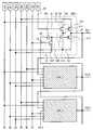
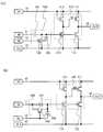
도 23에, 특허문헌 1에 기재된 구동 회로를 도시한다. 특허문헌 1의 구동 회로는, 트랜지스터(M1), 트랜지스터(M2), 트랜지스터(M3), 트랜지스터(M4) 및 용량 소자(C1)를 가진다. 특허문헌 1에서는, 신호(OUT)를 하이 레벨로 하는 경우에는, 트랜지스터(M1)의 게이트를 부유 상태로 하고, 용량 소자(C1)의 용량 결합을 사용하여 트랜지스터(M1)의 게이트의 전위를 전위(VDD)보다도 높게 하는 부트스트랩 동작이 행해지고 있다. 또한, 트랜지스터(M1)의 게이트를 부유 상태로 하기 위해서, 트랜지스터(M1)의 게이트와 접속되는 트랜지스터(예를 들면 트랜지스터(M4))의 게이트와 소스 사이의 전위차(이하, Vgs로 나타낸다)를 0[V]로 하고, 이 트랜지스터를 오프로 하는 것이 행해지고 있다.Fig. 23 shows a drive circuit disclosed in
또한, 신호(OUT)를 로우 레벨로 하는 경우에는, 신호(IN)를 하이 레벨로 하고, 트랜지스터(M2) 및 트랜지스터(M3)를 온으로 하는 것이 행해지고 있다.When the signal OUT is set to the low level, the signal IN is set to the high level and the transistor M2 and the transistor M3 are turned on.
트랜지스터가 가령 공핍형(노멀리 온 형이라고도 한다)인 경우에는, 트랜지스터의 Vgs를 0[V]로 해도, 트랜지스터가 오프로 되지 않는다. 따라서, 신호(OUT)를 하이 레벨로 하는 경우에 있어서, 트랜지스터(M3) 및 트랜지스터(M4)가 오프로 되지 않기 때문에, 트랜지스터(M1)의 게이트를 부유 상태로 할 수 없다. 트랜지스터(M1)의 게이트를 부유 상태로 할 수 없으면, 부트스트랩 동작을 정상적으로 행할 수 없어 오동작을 일으키는 경우가 있다. 또는, 오동작을 일으키지 않아도, 동작 가능한 구동 주파수의 범위가 좁아지는 경우가 있다.When the transistor is a depletion type (also referred to as a normally-on type), the transistor does not turn off even if Vgs of the transistor is 0 [V]. Therefore, when the signal OUT is set to the high level, the transistor M3 and the transistor M4 are not turned off, so that the gate of the transistor M1 can not be put in a floating state. If the gate of the transistor M1 can not be put in a floating state, the bootstrapping operation can not be performed normally and a malfunction may be caused. Alternatively, the range of the operable driving frequency may be narrowed without causing a malfunction.
또한, 신호(OUT)를 로우 레벨로 하는 경우에 있어서, 표시 장치의 구동 회로의 구동 전압은 크기 때문에, 트랜지스터(M2) 및 트랜지스터(M3)의 Vgs도 커진다. 따라서, 트랜지스터의 열화가 진행되어 결국 구동 회로가 오동작을 일으키는 경우가 있다.In addition, when the signal OUT is set to the low level, since the driving voltage of the driving circuit of the display device is large, the Vgs of the transistor M2 and the transistor M3 also become large. Therefore, the deterioration of the transistor proceeds and eventually the driving circuit may malfunction.
그래서, 본 발명의 일 형태에서는, 트랜지스터가 가령 공핍형이라도, 안정적으로 동작할 수 있는 반도체 장치를 제공하는 것을 과제의 하나로 한다. 또한, 트랜지스터의 열화를 억제하는 것을 과제의 하나로 한다.Therefore, in one aspect of the present invention, one of the problems is to provide a semiconductor device that can stably operate even if the transistor is a depletion type. One of the problems is to suppress deterioration of the transistor.
개시하는 발명의 일 형태인 반도체 장치는, 제 1 전위를 제 1 배선에 공급하는 기능을 갖는 제 1 트랜지스터와, 제 2 전위를 제 1 배선에 공급하는 기능을 갖는 제 2 트랜지스터와, 제 1 트랜지스터의 게이트에 제 1 트랜지스터가 온이 되기 위한 제 3 전위를 공급한 후, 제 3 전위의 공급을 멈추는 기능을 갖는 제 3 트랜지스터와, 제 2 전위를 제 1 트랜지스터의 게이트에 공급하는 기능을 갖는 제 4 트랜지스터와, 제 1 신호에 오프셋을 가한 제 2 신호를 생성하는 기능을 갖는 제 1 회로를 가진다. 그리고, 제 4 트랜지스터의 게이트에는, 제 2 신호가 입력된다. 또한 제 2 신호의 로우 레벨의 전위는, 제 2 전위 미만의 전위이다.A semiconductor device according to one aspect of the present invention includes a first transistor having a function of supplying a first potential to a first wiring, a second transistor having a function of supplying a second potential to a first wiring, A third transistor having a function of supplying a third potential for turning on the first transistor to the gate of the first transistor and then stopping the supply of the third potential to the gate of the first transistor, 4 transistor and a first circuit having a function of generating a second signal by offsetting the first signal. A second signal is input to the gate of the fourth transistor. The low level potential of the second signal is a potential lower than the second potential.
개시하는 발명의 일 형태인 반도체 장치는, 제 1 전위를 제 1 배선에 공급하는 기능을 갖는 제 1 트랜지스터와, 제 2 전위를 제 1 배선에 공급하는 기능을 갖는 제 2 트랜지스터와, 제 1 트랜지스터의 게이트에 제 1 트랜지스터가 온이 되기 위한 제 3 전위를 공급한 후, 제 3 전위의 공급을 멈추는 기능을 갖는 제 3 트랜지스터와, 제 2 전위를 제 1 트랜지스터의 게이트에 공급하는 기능을 갖는 제 4 트랜지스터와, 한쪽의 전극에 제 1 신호가 입력되는 용량 소자와, 용량 소자의 다른쪽의 전극에 제 4 전위를 공급하는 기능을 갖는 제 5 트랜지스터를 가진다. 그리고, 제 4 트랜지스터의 게이트에, 용량 소자의 다른쪽의 전극과 접속된다. 또한, 제 4 전위는, 제 2 전위 미만의 전위이다.A semiconductor device according to one aspect of the present invention includes a first transistor having a function of supplying a first potential to a first wiring, a second transistor having a function of supplying a second potential to a first wiring, A third transistor having a function of supplying a third potential for turning on the first transistor to the gate of the first transistor and then stopping the supply of the third potential to the gate of the first transistor, And a fifth transistor having a function of supplying a fourth potential to the other electrode of the capacitive element. The gate of the fourth transistor is connected to the other electrode of the capacitor. The fourth potential is a potential lower than the second potential.
또한, 상기 반도체 장치에 있어서, 제 2 트랜지스터의 게이트에는, 제 1 신호가 입력되어도 좋다.In the semiconductor device, a first signal may be input to the gate of the second transistor.
본 발명의 일 형태에 의해, 트랜지스터가 가령 공핍형이라도, 트랜지스터를 오프로 할 수 있다. 또한, 트랜지스터가 오프일 때의 드레인 전류를 작게 할 수 있다. 따라서, 회로의 오동작을 방지할 수 있다. 또한, 본 발명의 일 형태에 의해, 트랜지스터의 Vgs를 작게 할 수 있어 트랜지스터의 열화를 억제할 수 있다.According to an aspect of the present invention, even if the transistor is a depletion type transistor, the transistor can be turned off. Further, the drain current when the transistor is off can be reduced. Therefore, a malfunction of the circuit can be prevented. Further, according to the embodiment of the present invention, the Vgs of the transistor can be reduced, and deterioration of the transistor can be suppressed.
도 1은 본 발명의 일 형태에 따르는 반도체 장치를 설명하기 위한 도면.
도 2는 본 발명의 일 형태에 따르는 반도체 장치를 설명하기 위한 도면.
도 3은 본 발명의 일 형태에 따르는 반도체 장치를 설명하기 위한 도면.
도 4는 본 발명의 일 형태에 따르는 반도체 장치를 설명하기 위한 도면.
도 5는 본 발명의 일 형태에 따르는 반도체 장치를 설명하기 위한 도면.
도 6은 본 발명의 일 형태에 따르는 반도체 장치를 설명하기 위한 도면.
도 7은 본 발명의 일 형태에 따르는 반도체 장치를 설명하기 위한 도면.
도 8은 본 발명의 일 형태에 따르는 반도체 장치를 설명하기 위한 도면.
도 9는 본 발명의 일 형태에 따르는 반도체 장치를 설명하기 위한 도면.
도 10은 본 발명의 일 형태에 따르는 반도체 장치를 설명하기 위한 도면.
도 11은 본 발명의 일 형태에 따르는 시프트 레지스터 회로를 설명하기 위한 도면.
도 12는 본 발명의 일 형태에 따르는 시프트 레지스터 회로를 설명하기 위한 도면.
도 13은 본 발명의 일 형태에 따르는 표시 장치를 설명하기 위한 도면.
도 14는 본 발명의 일 형태에 따르는 산화물 재료의 구조를 설명하는 도면.
도 15는 본 발명의 일 형태에 따르는 산화물 재료의 구조를 설명하는 도면.
도 16은 본 발명의 일 형태에 따르는 산화물 재료의 구조를 설명하는 도면.
도 17은 본 발명의 일 형태에 따르는 트랜지스터의 구조를 설명하는 도면.
도 18은 산화물 반도체층을 사용한 트랜지스터 특성의 그래프.
도 19는 트랜지스터의 오프 전류와 측정시 기판 온도의 관계를 도시하는 도면.
도 20은 본 발명의 일 형태에 따르는 전자 기기를 설명하는 도면.
도 21은 본 발명의 일 형태에 따르는 전자 기기를 설명하는 도면.
도 22는 본 발명의 일 형태에 따르는 반도체 장치를 설명하기 위한 도면.
도 23은 종래의 구동 회로를 설명하는 도면.1 is a view for explaining a semiconductor device according to an embodiment of the present invention.
2 is a diagram for explaining a semiconductor device according to an embodiment of the present invention.
3 is a view for explaining a semiconductor device according to an embodiment of the present invention.
4 is a view for explaining a semiconductor device according to an embodiment of the present invention.
5 is a view for explaining a semiconductor device according to an embodiment of the present invention.
6 is a view for explaining a semiconductor device according to an embodiment of the present invention.
7 is a view for explaining a semiconductor device according to an embodiment of the present invention.
8 is a view for explaining a semiconductor device according to an embodiment of the present invention.
9 is a view for explaining a semiconductor device according to an embodiment of the present invention.
10 is a view for explaining a semiconductor device according to an embodiment of the present invention.
11 is a diagram for explaining a shift register circuit according to an embodiment of the present invention.
12 is a diagram for explaining a shift register circuit according to an aspect of the present invention.
13 is a view for explaining a display device according to an embodiment of the present invention.
14 is a view for explaining the structure of an oxide material according to an embodiment of the present invention.
15 is a view for explaining the structure of an oxide material according to an embodiment of the present invention.
16 is a view for explaining the structure of an oxide material according to an embodiment of the present invention.
17 is a view for explaining a structure of a transistor according to an embodiment of the present invention.
18 is a graph of transistor characteristics using an oxide semiconductor layer.
19 is a diagram showing the relationship between the off current of the transistor and the substrate temperature during the measurement.
20 is a view for explaining an electronic apparatus according to an embodiment of the present invention;
21 is a view for explaining an electronic apparatus according to an embodiment of the present invention;
22 is a view for explaining a semiconductor device according to an embodiment of the present invention.
23 is a view for explaining a conventional driving circuit;
본 발명을 설명하기 위한 실시형태의 일례에 관해서, 도면을 사용하여 이하에 설명한다. 또한, 본 발명의 취지 및 그 범위에서 일탈하지 않고 실시형태의 내용을 변경하는 것은, 당업자라면 용이하다. 따라서, 본 발명은, 이하에 나타내는 실시형태의 기재 내용으로 한정되지 않는다.An example of an embodiment for explaining the present invention will be described below with reference to the drawings. It is also easy for a person skilled in the art to change the contents of the embodiments without departing from the spirit and scope of the present invention. Therefore, the present invention is not limited to the description contents of the embodiments described below.
(실시형태 1)(Embodiment 1)
본 실시형태에서는, 입력 신호에 오프셋을 가한 신호를 생성하고, 상기 신호에 의해 구동하는 반도체 장치의 일례에 관해서 설명한다.In this embodiment, an example of a semiconductor device in which a signal obtained by adding an offset to an input signal is generated and driven by the signal is described.
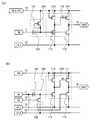
본 실시형태의 반도체 장치의 구성에 관해서 도 1a를 참조하여 설명한다. 도 1a는, 본 실시형태에 있어서의 반도체 장치의 회로도를 도시한다. 도 1a의 반도체 장치는, 회로(100)와, 회로(110)를 가진다. 회로(100)는, 배선(11), 배선(12), 배선(14) 및 회로(110)와 접속된다. 또한, 회로(110)는, 배선(15), 배선(13), 배선(16) 및 회로(100)와 접속된다. 또한, 회로(100) 및 회로(110)의 구성에 따라, 회로(100) 및 회로(110)와 접속되는 배선 등은 적절히 변경하면 좋다.The structure of the semiconductor device of the present embodiment will be described with reference to Fig. 1A. 1A shows a circuit diagram of a semiconductor device according to the present embodiment. The semiconductor device of FIG. 1A has a
또한, 명세서에 있어서는, X와 Y가 접속되어 있다, 라고 명시적으로 기재하는 경우에는, X와 Y가 전기적으로 접속되어 있는 경우와, X와 Y가 기능적으로 접속되어 있는 경우와, X와 Y가 직접 접속되어 있는 경우를 포함하는 것으로 한다.In the specification, when it is explicitly stated that X and Y are connected, the case where X and Y are electrically connected, the case where X and Y are functionally connected, the case where X and Y are electrically connected, Are directly connected to each other.
배선(13)에는 전위(VL1)가 공급된다. 전위(VL1)는 소정의 전위이다. 또한, 배선(13)은 전위(VL1)를 전달하는 기능을 가진다.A potential VL1 is supplied to the
배선(14)에는 전위(VL2)가 공급된다. 전위(VL2)는 소정의 전위이다. 또한, 전위(VL2)는 전위(VL1) 미만의 전위이다. 또한, 배선(14)은 전위(VL2)를 전달하는 기능을 가진다.A potential VL2 is supplied to the
배선(15)에는 전위(VH)가 공급된다. 전위(VH)는 소정의 전위이다. 또한, 전위(VH)는 전위(VL1)를 초과한 전위이다. 또한, 배선(15)은 전위(VH)를 전달하는 기능을 가진다.A potential VH is supplied to the
또한, 배선(13), 배선(14) 및 배선(15)을 전원선이라고도 한다. 또한, 전위(VL1), 전위(VL2) 및 전위(VH)를 전원 전위라고도 한다. 또한, 전위(VL1), 전위(VL2) 및 전위(VH)는, 예를 들면 전원 회로 등으로부터 공급된다.The
배선(11)에는 신호(IN)가 입력된다. 신호(IN)는 반도체 장치의 입력 신호이다. 또한, 신호(IN)는 디지털 신호이며, 신호(IN)의 하이 레벨의 전위는 VH이며, 신호(IN)의 로우 레벨의 전위는 VL1이다. 즉, 배선(11)에는 전위(VH)와 전위(VL1)가 선택적으로 공급된다. 또한, 배선(11)은 신호(IN)를 전달하는 기능을 가진다.A signal IN is input to the
배선(12)에는 신호(SE)가 입력된다. 신호(SE)는 오프셋 전압을 취득하는 타이밍을 제어하기 위한 신호이다. 또한, 신호(SE)는 디지털 신호이며, 신호(SE)의 하이 레벨의 전위는 VL2를 초과한 전위이며, 신호(SE)의 로우 레벨의 전위는 VL2 또는 VL2 미만의 전위이다. 즉, 배선(12)에는, 전위(VL2)를 초과한 전위와 전위(VL2) 또는 VL2 미만의 전위가 선택적으로 공급된다. 또한, 배선(12)은 신호(SE)를 전달하는 기능을 가진다.A signal SE is input to the
배선(16)으로부터는 신호(OUT)가 출력된다. 신호(OUT)는 반도체 장치의 출력 신호이다. 또한, 신호(OUT)는 디지털 신호이며, 신호(OUT)의 하이 레벨의 전위는 VH이며, 신호(OUT)의 로우 레벨의 전위는 VL1이다. 또한, 배선(16)은 신호(OUT)를 전달하는 기능을 가진다.And the signal OUT is outputted from the
또한, 배선(11), 배선(12) 및 배선(16)을 신호선이라고도 한다. 또한, 신호(IN)를 입력 신호, 신호(SE)를 제어 신호, 신호(OUT)를 출력 신호라고도 한다.The
회로(100)는, 신호(IN)에 오프셋을 가한 신호(INO)를 생성하는 기능을 가진다. 즉, 회로(100)는, 신호(IN)의 전위를 오프셋 전압분만큼 낮춘 신호(INO)를 생성하는 기능을 가진다. 또한, 회로(100)는, 신호(INO)를 회로(110)로 출력하는 기능을 가진다.The
또한, 신호(INO)의 로우 레벨의 전위는, 배선(13)의 전위(VL1)보다도 낮은 전위이다. 또한, 신호(INO)의 하이 레벨의 전위는 VL1을 초과하고, VH 미만의 전위인 것이 바람직하다.The potential of the low level of the signal INO is lower than the potential VL1 of the
회로(110)는, 신호(INO)(회로(100)의 출력 신호)에 따라, 신호(OUT)를 하이 레벨로 할지 로우 레벨로 할지를 선택하는 기능을 가진다. 예를 들면, 회로(110)가 인버터 회로로서 기능하는 경우, 회로(110)는, 신호(INO)가 하이 레벨일 때에는 신호(OUT)를 로우 레벨로 하고, 신호(INO)가 로우 레벨일 때에는 신호(OUT)를 하이 레벨로 하는 기능을 가진다. 또한, 회로(110)는, 신호(INO)에 따라, 배선(15)의 전위를 배선(16)으로 출력할지, 배선(13)의 전위를 배선(16)으로 출력할지를 선택하는 기능을 가진다. 예를 들면, 회로(110)는, 신호(INO)가 하이 레벨인 경우에 배선(13)의 전위를 배선(16)으로 출력하고, 신호(INO)가 로우 레벨인 경우에 배선(15)의 전위를 배선(16)으로 출력하는 기능을 가진다. 또한, 회로(110)는, 부트스트랩 동작에 의해, 신호(OUT)의 하이 레벨의 전위를 배선(15)의 전위(VH)와 동일하게 하는 기능을 가진다.The
다음에, 회로(100) 및 회로(110)의 구체적인 예에 관해서 도 1a를 참조하여 설명한다.Next, specific examples of the
회로(100)는, 용량 소자(101) 및 트랜지스터(102)를 가진다. 용량 소자(101)의 한쪽의 전극은 배선(11)과 접속된다. 트랜지스터(102)의 제 1 단자(소스 및 드레인의 한쪽이라고도 한다)는 배선(14)과 접속되고, 트랜지스터(102)의 제 2 단자는 용량 소자(101)의 다른쪽의 전극과 접속되고, 트랜지스터(102)의 게이트는 배선(12)과 접속된다.The
회로(110)는, 트랜지스터(111), 트랜지스터(112), 트랜지스터(113) 및 트랜지스터(114)를 가진다. 트랜지스터(111)의 제 1 단자는 배선(15)과 접속되고, 트랜지스터(111)의 제 2 단자는 배선(16)과 접속된다. 트랜지스터(112)의 제 1 단자는 배선(13)과 접속되고, 트랜지스터(112)의 제 2 단자는 배선(16)과 접속되고, 트랜지스터(112)의 게이트는 트랜지스터(114)의 게이트와 접속된다. 트랜지스터(113)의 제 1 단자는 배선(15)과 접속되고, 트랜지스터(113)의 제 2 단자는 트랜지스터(111)의 게이트와 접속되고, 트랜지스터(113)의 게이트는 배선(15)과 접속된다. 트랜지스터(114)의 제 1 단자는 배선(13)과 접속되고, 트랜지스터(114)의 제 2 단자는 트랜지스터(111)의 게이트와 접속되고, 트랜지스터(114)의 게이트는 용량 소자(101)의 다른쪽의 전극과 접속된다. 또한, 트랜지스터(111)의 게이트와 다른 트랜지스터(예를 들면, 트랜지스터(113), 트랜지스터(114) 등)의 접속 개소를 노드(N1)로 한다.The
용량 소자(101)는, 배선(11)과 트랜지스터(102)의 제 2 단자 사이의 전위차를 유지하는 기능을 가진다. 따라서, 트랜지스터(102)의 제 2 단자가 부유 상태가 되는 경우에는, 배선(11)에 입력되는 신호에 따라, 트랜지스터(102)의 제 2 단자의 전위도 변동된다. 즉, 신호(IN)에 따라, 신호(INO)의 전위도 변동된다.The
트랜지스터(102)는, 배선(14)의 전위(VL2)를 용량 소자(101)의 다른쪽의 전극에 공급하는 기능을 가진다. 트랜지스터(102)가 용량 소자(101)의 다른쪽의 전극에 전위(VL2)를 공급하는 타이밍은, 배선(12)의 신호(SE)에 의해 제어된다.The
또한, 트랜지스터(102)는, 전위(VL1) 미만의 전위를 용량 소자(101)의 다른쪽의 전극에 공급하면 좋다. 구체적으로는, 트랜지스터(102)는, 트랜지스터(114)의 제 1 단자의 전위 미만의 전위를, 용량 소자(101)의 다른쪽의 전극에 공급하면 좋다.The
트랜지스터(111)는, 배선(15)의 전위(VH)를 배선(16)에 공급하는 기능을 가진다. 또한, 트랜지스터(111)는, 게이트와 제 2 단자 사이의 전위차를 유지하는 기능을 가진다. 따라서, 노드(N1)가 부유 상태인 경우에는, 배선(16)의 전위가 상승하면, 노드(N1)의 전위도 상승한다.The
또한, 배선(15)에 신호가 입력되는 경우에는, 트랜지스터(111)는, 배선(15)의 신호를 배선(16)에 공급하는 기능을 가진다.When a signal is input to the
트랜지스터(112)는, 배선(13)의 전위(VL1)를 배선(16)에 공급하는 기능을 가진다. 트랜지스터(112)가 전위(VL1)를 배선(16)에 공급하는 타이밍은, 회로(100)로부터 출력되는 신호(INO)(용량 소자(101)의 다른쪽의 전극의 전위)에 의해 제어된다.The
트랜지스터(113)는, 배선(15)의 전위(VH)를 트랜지스터(111)의 게이트에 공급하는 기능을 가진다. 또한, 트랜지스터(113)는, 트랜지스터(111)의 게이트에 전위(VH)를 공급한 후, 트랜지스터(111)의 게이트로의 전위(VH)의 공급을 멈추는 기능을 가진다. 또한, 트랜지스터(113)는, 트랜지스터(111)가 온이 된 후부터 트랜지스터(113)가 오프가 될 때까지, 트랜지스터(111)의 게이트에 전위(VH)를 공급하는 기능을 가진다.The
또한, 트랜지스터(113)가 트랜지스터(111)의 게이트에 공급하는 전위는, 트랜지스터(111)가 온이 되는 전위이면 좋다.The potential that the
트랜지스터(114)는, 배선(13)의 전위(VL1)를 트랜지스터(111)의 게이트에 공급하는 기능을 가진다. 트랜지스터(114)가 전위(VL1)를 트랜지스터(111)의 게이트에 공급하는 타이밍은, 회로(100)로부터 출력되는 신호(INO)에 의해 제어된다.The
또한, 본 실시형태의 반도체 장치가 갖는 트랜지스터(예를 들면 트랜지스터(102), 트랜지스터(111), 트랜지스터(112), 트랜지스터(113) 및 트랜지스터(114))는 동일한 도전형이다. 본 실시형태에서는, 본 실시형태의 반도체 장치가 갖는 트랜지스터가 N채널형인 것으로서 설명한다.The transistors (for example, the
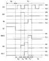
다음에, 도 1a의 반도체 장치의 구동 방법의 일례에 관해서, 도 1b를 참조하여 설명한다. 도 1b는, 도 1a의 반도체 장치의 구동 방법을 설명하기 위한 타이밍 차트의 일례이다.Next, an example of a method of driving the semiconductor device of Fig. 1A will be described with reference to Fig. 1B. 1B is an example of a timing chart for explaining the driving method of the semiconductor device of FIG. 1A.
도 1a의 반도체 장치의 구동 방법에 관해서 기간(T0)과 기간(T1)으로 나누어 설명한다.The driving method of the semiconductor device of FIG. 1A is divided into a period T0 and a period T1.
기간(T0)은, 용량 소자(101)에 오프셋 전압을 유지시키기 위한 기간이다. 우선, 신호(IN)를 로우 레벨로 하고, 용량 소자(101)의 한쪽의 전극의 전위를 VL1로 한다. 또한, 신호(SE)를 하이 레벨로 하고, 트랜지스터(102)를 온으로 한다. 그리고, 배선(14)의 전위(VL2)를 용량 소자(101)의 다른쪽의 전극에 공급하고, 용량 소자(101)의 다른쪽의 전극의 전위를 VL2로 한다. 따라서, 용량 소자(101)에는, 신호(IN)의 로우 레벨의 전위(VL1)와, 트랜지스터(102)에 의해 공급되는 배선(14)의 전위(VL2)의 차(VL1-VL2)를 유지시킨다. 이 차(VL1-VL2)가 오프셋 전압에 상당한다.The period T0 is a period for maintaining the offset voltage in the
또한, 기간(T0)에 있어서는, 트랜지스터(102)는 VL1 미만의 전위를 용량 소자(101)의 다른쪽의 전극에 공급하면 좋다.In the period T0, the
기간(T1)은, 신호(IN)에 오프셋을 가하여 신호(INO)를 생성하고, 신호(INO)에 의해 회로(110)를 구동하기 위한 기간이다. 우선, 신호(SE)를 로우 레벨로 하고, 트랜지스터(102)를 오프로 함으로써, 용량 소자(101)의 다른쪽의 전극을 부유 상태로 한다. 용량 소자(101)는, 기간(T0)에 있어서 전위차(VL1-VL2)를 유지하고 있기 때문에, 신호(IN)로부터 전위차(VL1-VL2)에 따른 값을 뺀 신호인 신호(INO)가 생성된다. 따라서, 신호(IN)가 로우 레벨이 되면, 신호(INO)도 로우 레벨이 되고, 신호(INO)의 로우 레벨의 전위는 VL1 미만의 전위가 된다. 또한, 신호(IN)가 하이 레벨이 되면, 신호(INO)도 하이 레벨이 되고, 신호(INO)의 하이 레벨의 전위는 VH 미만의 전위가 된다.The period T1 is a period for applying an offset to the signal IN to generate the signal INO and driving the
기간(T1)에 있어서의 도 1a의 반도체 장치의 구동 방법에 관해서, 신호(IN)가 하이 레벨인 경우와 로우 레벨인 경우로 나누어 설명한다.The driving method of the semiconductor device of FIG. 1A in the period T1 will be described separately in the case where the signal IN is at the high level and the case where the signal IN is at the low level.
기간(T1)에 있어서, 신호(IN)가 하이 레벨이 되면, 신호(INO)도 하이 레벨이 되기 때문에, 트랜지스터(112) 및 트랜지스터(114)가 온이 된다. 따라서, 배선(13)의 전위(VL1)가 트랜지스터(112)에 의해 배선(16)에 공급된다. 또한, 배선(13)의 전위(VL1)가 트랜지스터(114)에 의해 노드(N1)에 공급된다. 노드(N1)에는, 트랜지스터(113)에 의해 배선(15)의 전위(VH)도 공급되고 있다. 그러나, 트랜지스터(114)의 W(채널 폭)/L(채널 길이) 비를 트랜지스터(113)의 W/L 비보다도 충분히 크게 해 두면, 노드(N1)의 전위는 트랜지스터(111)가 오프가 될 정도의 전위가 되기 때문에, 트랜지스터(111)는 오프가 된다. 따라서, 신호(OUT)는 로우 레벨이 되고, 그 전위는 VL1이 된다.In the period T1, when the signal IN becomes a high level, the signal INO also becomes a high level, so that the
한편, 기간(T1)에 있어서, 신호(IN)가 로우 레벨이 되면, 신호(INO)도 로우 레벨이 되기 때문에, 트랜지스터(112) 및 트랜지스터(114)가 오프가 된다. 노드(N1)에는, 트랜지스터(113)에 의해 배선(15)의 전위(VH)가 공급되기 때문에, 노드(N1)의 전위가 상승한다. 따라서, 트랜지스터(111)가 온이 되고, 배선(15)의 전위(VH)가 트랜지스터(111)에 의해 배선(16)으로 공급되기 때문에, 배선(16)의 전위가 상승한다. 드디어, 노드(N1)의 전위가 전위(VH)로부터 트랜지스터(113)의 임계값 전압을 뺀 전위까지 상승하면, 트랜지스터(113)가 오프가 되고, 노드(N1)가 부유 상태가 된다. 노드(N1)가 부유 상태가 되어도, 배선(16)의 전위는 상승하고 있다. 또한, 트랜지스터(111)의 게이트와 제 2 단자 사이에는, 트랜지스터(113)가 오프가 되었을 때의 노드(N1)와 배선(16)의 전위차가 유지되고 있다. 따라서, 배선(16)의 전위의 상승에 따라, 노드(N1)의 전위가 더욱 상승하고, 전위(VH)보다도 높아진다. 소위 부트스트랩 동작이다. 따라서, 신호(OUT)가 하이 레벨이 되고, 그 전위는 VH가 된다.On the other hand, in the period T1, when the signal IN becomes a low level, the signal INO also becomes a low level, so that the
또한, 배선(15)에 신호가 입력되어 있는 경우, 배선(15)의 신호가 배선(16)으로 출력된다. 예를 들면, 배선(15)에 클록 신호가 입력되는 경우, 신호(IN)가 로우 레벨인 기간에서는, 클록 신호가 배선(15)으로부터 배선(16)으로 출력된다.Further, when a signal is input to the
이상과 같이, 신호(OUT)를 하이 레벨로 하는 경우에는, 트랜지스터(114)의 게이트의 전위가 VL1 미만이 되기 때문에, 트랜지스터(114)의 Vgs를 음의 값으로 할 수 있다. 따라서, 가령 트랜지스터(114)가 공핍형이라도, 트랜지스터(114)를 오프로 할 수 있다. 또는, 가령 트랜지스터(114)의 Vgs가 0[V]인 경우의 드레인 전류가 큰 트랜지스터라도, 트랜지스터(114)의 드레인 전류를 작게 할 수 있다. 따라서, 트랜지스터(111)의 게이트를 부유 상태로 할 수 있고, 회로(110)의 오동작을 방지할 수 있다.As described above, when the signal OUT is set to the high level, since the potential of the gate of the
또한, 트랜지스터(114)와 같이 트랜지스터(112)의 Vgs도 음의 값으로 할 수 있다. 따라서, 가령 트랜지스터(112)가 공핍형이라도, 트랜지스터(112)를 오프로 할 수 있다. 또는, 가령 트랜지스터(112)의 Vgs가 0[V]인 경우의 드레인 전류가 큰 트랜지스터라도, 트랜지스터(112)의 드레인 전류를 작게 할 수 있다. 따라서, 배선(16)으로부터 배선(13)으로 흐르는 전류를 방지 또는 억제할 수 있기 때문에, 소비 전력의 삭감을 도모할 수 있다.Also, Vgs of the
또한, 신호(OUT)를 로우 레벨로 하는 경우에는, 트랜지스터(112) 및 트랜지스터(114)의 게이트의 전위는 VH 미만의 전위가 되기 때문에, 트랜지스터(112) 및 트랜지스터(114)의 Vgs를 작게 할 수 있다. 따라서, 트랜지스터(112) 및 트랜지스터(114)의 열화를 억제할 수 있다.When the signal OUT is set to a low level, the potentials of the gates of the
이상, 도 1a의 반도체 장치의 구동 방법에 관해서 설명하였다.The driving method of the semiconductor device of FIG. 1A has been described above.
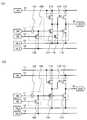
다음에, 도 1a와는 상이한 반도체 장치에 관해서, 도 2a, 도 2b, 도 3a, 도 3b, 도 4a, 도 4b, 도 5a, 도 5b를 참조하여 설명한다. 또한, 이하에서는, 도 1a와 상이한 부분에 관해서 설명한다.Next, a semiconductor device different from that of FIG. 1A will be described with reference to FIGS. 2A, 2B, 3A, 3B, 4A, 4B, 5A and 5B. In the following, the parts different from FIG. 1A will be described.
도 2a에 도시하는 바와 같이, 도 1a의 반도체 장치에 있어서, 배선(14)을 생략하고, 트랜지스터(102)의 제 1 단자를 배선(13)과 접속해도 좋다. 그리고, 기간(T0)에 있어서 배선(13)에 전위(VL2)를 공급하고, 기간(T1)에 있어서 배선(13)에 전위(VL1)를 공급해도 좋다. 이 경우에도, 기간(T0)에 있어서 용량 소자(101)의 다른쪽의 전극에 전위(VL2)를 공급할 수 있기 때문에, 도 1a의 반도체 장치와 같은 동작을 행할 수 있다. 따라서, 도 1a의 반도체 장치와 같은 효과를 나타낼 수 있다. 또한, 배선(14)을 생략할 수 있기 때문에, 도 1a의 반도체 장치와 비교하여 배선의 수를 감소시킬 수 있다.As shown in Fig. 2A, in the semiconductor device of Fig. 1A, the
또한, 도 2a의 반도체 장치에 있어서, 기간(T0)에 있어서 배선(13)의 전위를 전위(VL1) 그대로로 하고, 배선(11)의 전위를 전위(VL1)를 초과하고, 전위(VH) 미만의 전위로 해도 좋다. 이 경우에도, 기간(T1)에 있어서, 신호(IN)가 로우 레벨인 경우에, 용량 소자(101)의 다른쪽의 전극의 전위를 전위(VL1) 미만으로 할 수 있기 때문에, 도 1a의 반도체 장치와 같은 동작을 행할 수 있다. 따라서, 도 1a의 반도체 장치와 같은 효과를 나타낼 수 있다. 또한, 전원 전위를 일정하게 할 수 있기 때문에, 배선(13)에 전위를 공급하는 전원 회로 등의 구성을 간단하게 할 수 있다.2A, when the potential of the
도 2b에 도시하는 바와 같이, 도 1a의 반도체 장치에 있어서, 배선(14)을 생략하고, 트랜지스터(102)의 제 1 단자를 배선(15)과 접속해도 좋다. 그리고, 기간(T0)에 있어서 배선(15)에 전위(VL2)를 공급하고, 기간(T1)에 있어서 배선(15)에 전위(VH)를 공급해도 좋다. 이 경우에도, 기간(T0)에 있어서 용량 소자(101)의 다른쪽의 전극에 전위(VL2)를 공급할 수 있기 때문에, 도 1a의 반도체 장치와 같은 동작을 행할 수 있다. 따라서, 도 1a의 반도체 장치와 같은 효과를 나타낼 수 있다. 또한, 배선(14)을 생략할 수 있기 때문에, 도 1a의 반도체 장치와 비교하여 배선의 수를 감소시킬 수 있다.As shown in FIG. 2B, in the semiconductor device of FIG. 1A, the
도 3a에 도시하는 바와 같이, 도 1a의 반도체 장치에 있어서, 배선(14)을 생략하고, 트랜지스터(102)의 제 1 단자를 배선(12)과 접속하고, 트랜지스터(102)의 제 2 단자 및 게이트를 용량 소자(101)의 다른쪽의 전극과 접속해도 좋다. 그리고, 기간(T0)에 있어서 신호(SE)를 로우 레벨로 하고, 기간(T1)에 있어서 신호(SE)를 하이 레벨로 해도 좋다. 이 경우에도, 기간(T0)에 있어서 용량 소자(101)의 다른쪽의 전극을 전위(VL1) 미만으로 할 수 있기 때문에, 도 1a의 반도체 장치와 같은 동작을 행할 수 있다. 따라서, 도 1a의 반도체 장치와 같은 효과를 나타낼 수 있다. 또한, 배선(14)을 생략할 수 있기 때문에, 도 1a의 반도체 장치와 비교하여 배선의 수를 감소시킬 수 있다.3A, the
도 3b에 도시하는 바와 같이, 도 1a의 반도체 장치에 있어서, 배선(12) 및 배선(14)을 생략하고, 트랜지스터(102)의 제 1 단자를 배선(13)과 접속하고, 트랜지스터(102)의 제 2 단자 및 게이트를 용량 소자(101)의 다른쪽의 전극과 접속해도 좋다. 그리고, 기간(T0)에 있어서 배선(13)에 전위(VL2)를 공급하고, 기간(T1)에 있어서 배선(13)에 전위(VL1)를 공급해도 좋다. 이 경우에도, 기간(T0)에 있어서 용량 소자(101)의 다른쪽의 전극을 전위(VL1) 미만으로 할 수 있기 때문에, 도 1a의 반도체 장치와 같은 동작을 행할 수 있다. 따라서, 도 1a의 반도체 장치와 같은 효과를 나타낼 수 있다. 또한, 배선(12) 및 배선(14)을 생략할 수 있기 때문에, 도 1a의 반도체 장치와 비교하여 배선의 수를 감소시킬 수 있다.The
도 4a에 도시하는 바와 같이, 도 1a의 반도체 장치에 있어서, 배선(12) 및 배선(14)을 생략하고, 트랜지스터(102)의 제 1 단자를 배선(15)과 접속하고, 트랜지스터(102)의 제 2 단자 및 게이트를 용량 소자(101)의 다른쪽의 전극과 접속해도 좋다. 그리고, 기간(T0)에 있어서 배선(15)에 전위(VL2)를 공급하고, 기간(T1)에 있어서 배선(15)에 전위(VH)를 공급해도 좋다. 이 경우에도, 기간(T0)에 있어서 용량 소자(101)의 다른쪽의 전극을 전위(VL1) 미만으로 할 수 있기 때문에, 도 1a의 반도체 장치와 같은 동작을 행할 수 있다. 따라서, 도 1a의 반도체 장치와 같은 효과를 나타낼 수 있다. 또한, 배선(12) 및 배선(14)을 생략할 수 있기 때문에, 도 1a의 반도체 장치와 비교하여 배선의 수를 감소시킬 수 있다.The
도 4b에 도시하는 바와 같이, 도 1a의 반도체 장치에 있어서, 트랜지스터(112)의 게이트를 배선(11)과 접속해도 좋다. 도 4b의 반도체 장치에서는, 트랜지스터(112)가 배선(13)의 전위(VL1)를 배선(16)에 공급하는 타이밍은 신호(IN)에 의해 제어된다. 신호(IN)는 신호(INO)보다도 하강 시간 및 상승 시간이 짧기 때문에, 트랜지스터(112)의 게이트가 용량 소자(101)의 다른쪽의 전극과 접속되는 경우와 비교하여, 트랜지스터(112)가 온 또는 오프가 되는 타이밍을 빠르게 할 수 있다. 따라서, 배선(13)의 전위(VL1)를 배선(16)에 공급하는 타이밍도 빨라지기 때문에, 신호(OUT)의 하강 시간을 짧게 할 수 있다. 또한, 트랜지스터(112)가 오프가 되는 타이밍이 빨라지면, 배선(15)과 배선(13) 사이의 관통 전류가 생기는 시간을 짧게 할 수 있기 때문에, 소비 전력의 삭감을 도모할 수 있다.As shown in Fig. 4B, the gate of the
또한, 도 4b의 반도체 장치와 같이, 도 2a, 도 2b, 도 3a, 도 3b, 및 도 4a의 반도체 장치에 있어서도, 트랜지스터(112)의 게이트를 배선(11)과 접속해도 좋다. 이 경우에도, 도 4b의 반도체 장치와 같은 효과를 나타낼 수 있다.2A, 2B, 3A, 3B, and 4A, the gate of the
도 5a에 도시하는 바와 같이, 도 1a의 반도체 장치에 있어서, 제 1 단자가 배선(13)과 접속되고, 제 2 단자가 트랜지스터(111)의 게이트와 접속되고, 게이트가 배선(12)과 접속된 트랜지스터(115)를 형성해도 좋다. 트랜지스터(115)는, 배선(13)의 전위(VL1)를 트랜지스터(111)의 게이트에 공급하는 기능을 가진다. 트랜지스터(115)가 트랜지스터(111)의 게이트에 전위(VL1)를 공급하는 타이밍은, 배선(12)의 신호(SE)에 의해 제어된다. 도 5a의 반도체 장치에서는, 기간(T0)에 있어서 배선(13)의 전위(VL1)를 트랜지스터(111)의 게이트에 공급할 수 있기 때문에, 반도체 장치를 초기화할 수 있다. 따라서, 반도체 장치의 오동작을 방지할 수 있다.1A, the first terminal is connected to the
또한, 도 5a의 반도체 장치에 있어서, 트랜지스터(115)의 제 1 단자를 배선(14)과 접속해도 좋다. 이 경우에도, 트랜지스터(115)의 제 1 단자가 배선(13)과 접속되는 경우와 같은 동작을 행할 수 있다.In the semiconductor device of Fig. 5A, the first terminal of the
또한, 오프셋 전압을 취득하는 타이밍과, 초기화를 행하는 타이밍이 상이한 경우에는, 트랜지스터(115)의 게이트를 초기화용 신호가 입력되는 배선과 접속해도 좋다.Further, when the timing for obtaining the offset voltage differs from the timing for performing the initialization, the gate of the
또한, 도 2a, 도 2b, 도 3a, 도 3b, 도 4a 및 도 4b의 반도체 장치에 있어서도, 제 1 단자가 배선(13) 또는 배선(14)과 접속되고, 제 2 단자가 트랜지스터(111)의 게이트와 접속되고, 게이트가 배선(12)과 접속된 트랜지스터(115)를 형성해도 좋다. 이 경우에도, 도 5a의 반도체 장치와 같은 효과를 나타낼 수 있다.Also in the semiconductor device of FIGS. 2A, 2B, 3A, 3B and 4A and 4B, the first terminal is connected to the
도 5b에 도시하는 바와 같이, 도 1a의 반도체 장치에 있어서, 트랜지스터(113)의 제 2 단자 및 게이트를 배선(17)과 접속해도 좋다. 배선(17)에는, 전위(VH)를 공급해도 좋고, 전위(VL1)를 초과하고, 전위(VH) 미만의 전위를 공급해도 좋고, 신호를 입력해도 좋다. 배선(17)에 입력하는 신호의 예로서는, 신호(IN)의 반전 신호가 있다. 따라서, 배선(11)이 인버터 회로를 개재하여 배선(17)과 접속되어도 좋다. 이와 같이 하면, 트랜지스터(114)가 온이 될 때, 트랜지스터(113)가 오프가 되기 때문에, 배선(15)과 배선(13) 사이에 전류가 흐르는 것을 방지할 수 있다. 따라서, 소비 전력의 삭감을 도모할 수 있다. 또한, 트랜지스터(113)의 W/L 비보다도, 트랜지스터(114)의 W/L 비를 충분히 크게 할 필요가 없어지기 때문에, 트랜지스터의 사이즈를 작게 할 수 있다.As shown in Fig. 5B, the second terminal and the gate of the
또한, 도 2a, 도 2b, 도 3a, 도 3b, 도 4a, 도 4b 및 도 5a의 반도체 장치에 있어서도, 트랜지스터(113)의 제 2 단자 및 게이트를 배선(17)과 접속해도 좋다. 이 경우에도, 도 5b의 반도체 장치와 같은 효과를 나타낼 수 있다.Also in the semiconductor device of Figs. 2A, 2B, 3A, 3B, 4A, 4B and 5A, the second terminal and the gate of the
도 22a에 도시하는 바와 같이, 도 1a의 반도체 장치에 있어서, 배선(14)을 생략하고, 트랜지스터(102)의 제 1 단자를 배선(13)과 접속하고, 한쪽의 전극이 배선(12)과 접속되고 또한 다른쪽의 전극이 용량 소자(101)의 다른쪽의 전극과 접속되는 용량 소자(103)를 형성해도 좋다. 용량 소자(103)는 배선(12)과 용량 소자(101)의 다른쪽의 전극 사이의 전위차를 유지하는 기능을 가진다. 또한, 도 22a의 반도체 장치는, 트랜지스터(102)는 배선(13)의 전위(VL1)를 용량 소자(101)의 다른쪽의 전극에 공급하는 기능을 가진다. 도 22a의 반도체 장치는, 기간(T0)에 있어서, 용량 소자(101)의 한쪽의 전극에는 로우 레벨의 신호(IN)가 입력되고, 용량 소자(101)의 다른쪽의 전극에는 배선(13)의 전위(VL1)가 트랜지스터(102)에 의해 공급된다. 그 후, 신호(SE)가 하이 레벨에서 로우 레벨이 되면, 트랜지스터(102)가 오프가 되고, 또한 용량 소자(101)의 다른쪽의 전극의 전위는 용량 소자(103)의 용량 결합에 의해 전위(VL1)로부터 저하된다. 따라서, 기간(T0)에 있어서 용량 소자(101)의 다른쪽의 전극을 전위(VL1) 미만으로 할 수 있기 때문에, 도 1a의 반도체 장치와 같은 동작을 행할 수 있다. 따라서, 도 1a의 반도체 장치와 같은 효과를 나타낼 수 있다. 또한, 배선(14)을 생략할 수 있기 때문에, 도 1a의 반도체 장치와 비교하여 배선의 수를 감소시킬 수 있다. 또한, 전위(VL2)를 필요로 하지 않기 때문에, 전원 전위의 수를 감소시킬 수 있다.1A, the
도 22b에 도시하는 바와 같이, 도 22a의 반도체 장치에 있어서, 트랜지스터(102)의 제 1 단자를 배선(11)과 접속해도 좋다. 이 경우에도, 기간(T0)에 있어서, 로우 레벨의 신호(IN)를 트랜지스터(102)에 의해 용량 소자(101)의 다른쪽의 전극에 공급할 수 있기 때문에, 도 22a의 반도체 장치와 같은 동작을 행할 수 있다. 따라서, 도 22a의 반도체 장치와 같은 효과를 나타낼 수 있다.As shown in Fig. 22B, the first terminal of the
또한, 도 22a 및 도 22b의 반도체 장치에 있어서, 용량 소자(103)를 생략해도 좋다. 이 경우에는, 용량 소자(103) 대신에, 트랜지스터(102)의 게이트와 제 2 단자 사이의 기생 용량을 사용하면 좋다.In the semiconductor device of Figs. 22A and 22B, the
또한, 도 22a 및 도 22b의 반도체 장치에 있어서, 용량 소자(103)의 한쪽의 전극을 배선(12)과는 상이한 새로운 배선과 접속해도 좋다. 이 배선에 입력하는 신호는, 기간(T0)에 있어서 신호(SE)가 하이 레벨에서 로우 레벨이 된 후에, 하이 레벨에서 로우 레벨이 되는 신호인 것이 바람직하다. 이와 같이 하면, 트랜지스터(102)가 오프가 된 후에, 용량 소자(101)의 다른쪽의 전극의 전위를 낮출 수 있다. 또한, 로우 레벨에서 하이 레벨이 되는 타이밍은, 신호(SE)가 하이 레벨인 기간인 것이 바람직하다.In the semiconductor device of Figs. 22A and 22B, one electrode of the
또한, 도 2a, 도 2b, 도 3a, 도 3b, 도 4a, 도 4b, 도 5a 및 도 5b의 반도체 장치에 있어서도, 배선(14)을 생략하고, 트랜지스터(102)의 제 1 단자를 배선(11) 또는 배선(13)과 접속하고, 한쪽의 전극이 배선(12)과 접속되고 또한 다른쪽의 전극이 용량 소자(101)의 다른쪽의 전극과 접속되는 용량 소자(103)를 형성해도 좋다.Also in the semiconductor device of FIGS. 2A, 2B, 3A, 3B, 4A, 4B, 5A and 5B, the
도시는 하지 않지만, 도 2a, 도 2b, 도 3a, 도 3b, 도 4a, 도 4b, 도 5a, 도 5b, 도 22a 및 도 22b의 반도체 장치에 있어서, 트랜지스터(111)의 게이트와 제 2 단자 사이에 용량 소자를 접속해도 좋다. 이와 같이 하면, 배선(16)과 노드(N1) 사이의 용량값을 크게 할 수 있다. 따라서, 트랜지스터(111)의 게이트와 제 2 단자 사이에 용량 소자가 형성되어 있지 않은 경우와 비교하여, 신호(IN)가 로우 레벨인 기간에 있어서 노드(N1)를 보다 높게 할 수 있다. 즉, 트랜지스터(111)의 Vgs를 크게 할 수 있다. 따라서, 트랜지스터(111)의 드레인 전류를 크게 할 수 있고, 신호(OUT)의 상승 시간을 짧게 할 수 있다.In the semiconductor device of FIGS. 2A, 2B, 3A, 3B, 4A, 4B, 5A, 5B, 22A and 22B, the gate of the
도시는 하지 않지만, 도 2a, 도 2b, 도 3a, 도 3b, 도 4a, 도 4b, 도 5a, 도 5b, 도 22a 및 도 22b의 반도체 장치에 있어서, 용량 소자(101)로서 MOS 용량을 사용해도 좋다. 이 경우, MOS 용량으로서 사용하는 트랜지스터의 게이트를 배선(11)과 접속하고, 트랜지스터의 소스 또는 드레인을 트랜지스터(102)의 제 2 단자와 접속하는 것이 바람직하다. 이와 같이 하면, 배선(11)의 전위는 트랜지스터(102)의 제 2 단자의 전위보다도 높기 때문에, 단위 면적당 용량값을 크게 할 수 있다.In the semiconductor device of FIGS. 2A, 2B, 3A, 3B, 4A, 4B, 5A, 5B, and 22A and 22B, MOS capacitors are used as the
이상, 도 1a와는 상이한 구성의 반도체 장치에 관해서 설명하였다.The semiconductor device having the configuration different from that of FIG. 1A has been described above.
또한, 트랜지스터(111)의 W/L 비가 클 수록, 신호(OUT)의 상승 시간을 짧게 할 수 있다. 따라서, 트랜지스터(111)의 W/L 비는, 반도체 장치가 갖는 트랜지스터 중에서 가장 큰 것이 바람직하다. 즉, 트랜지스터(111)의 W/L 비는, 트랜지스터(102)의 W/L 비, 트랜지스터(112)의 W/L 비, 트랜지스터(113)의 W/L 비, 및 트랜지스터(114)의 W/L 비보다도 큰 것이 바람직하다.Further, the larger the W / L ratio of the
또한, 트랜지스터(112)는 배선(16)과 접속된 부하에 전위를 공급하는데 대해, 트랜지스터(114)는 트랜지스터(111)의 게이트에 전위를 공급한다. 또한, 트랜지스터(112)의 W/L 비가 클 수록, 신호(OUT)의 하강 시간을 짧게 할 수 있다. 따라서, 트랜지스터(112)의 W/L 비는, 트랜지스터(114)의 W/L 비보다도 큰 것이 바람직하다.Further, the
또한, 트랜지스터(102)는 기간(T0)에 있어서 용량 소자(101)의 다른쪽의 전극에 전하를 공급하면 되기 때문에, 트랜지스터(102)의 W/L 비를 크게 할 필요는 없다. 따라서, 트랜지스터(102)의 W/L 비는, 트랜지스터(112) 또는 트랜지스터(114)의 W/L 비보다도 작은 것이 바람직하다.It is not necessary to increase the W / L ratio of the
또한, 용량 소자(101)의 용량값이 트랜지스터(112)의 게이트 용량 및 트랜지스터(114)의 게이트 용량의 합보다도 클 수록, 신호(INO)의 진폭 전압을 신호(IN)의 진폭 전압에 가깝게 할 수 있다. 따라서, 용량 소자(101)의 용량값은, 트랜지스터(112)의 게이트 용량 및 트랜지스터(114)의 게이트 용량의 합보다도 큰 것이 바람직하다. 또한, 용량 소자(101)의 한쪽의 전극이 트랜지스터의 게이트 전극과 동일한 재료이며, 용량 소자(101)의 다른쪽의 전극이 트랜지스터의 소스 전극 또는 드레인 전극과 동일한 재료인 경우, 용량 소자(101)의 한쪽의 전극과 다른쪽의 전극이 중첩되는 면적은, 트랜지스터(112)의 게이트와 소스가 중첩되는 면적, 트랜지스터(112)의 게이트와 드레인이 중첩되는 면적, 트랜지스터(114)의 게이트와 소스가 중첩되는 면적, 및 트랜지스터(114)의 게이트와 드레인이 중첩되는 면적의 합보다도 큰 것이 바람직하다.Further, as the capacitance value of the
또한, 기간(T0)에 있어서, 배선(13)에 전위(VL1)를 공급하지 않고, 배선(13)을 부유 상태로 해도 좋다. 또는, 기간(T0)에 있어서, 배선(15)에 전위(VH)를 공급하지 않고, 배선(15)을 부유 상태로 해도 좋다. 이와 같이 하면, 기간(T0)에 있어서의 오동작을 방지할 수 있다.In the period T0, the potential VL1 may not be supplied to the
또한, 기간(T1)에 있어서, 배선(14)에 전위(VL2)를 공급하지 않고, 배선(14)을 부유 상태로 해도 좋다.In the period T1, the potential VL2 may not be supplied to the
또한, 신호(IN)가 하이 레벨이 되는 기간에 있어서, 로우 레벨이 되는 신호를 배선(15)에 입력해도 좋다. 이와 같이 하면, 트랜지스터(114)가 온이 될 때, 트랜지스터(113)가 오프가 되기 때문에, 배선(15)과 배선(13) 사이에 전류가 흐르는 것을 방지할 수 있다. 따라서, 소비 전력의 삭감을 도모할 수 있다. 또한, 트랜지스터(113)의 W/L 비보다도, 트랜지스터(114)의 W/L 비를 충분히 크게 할 필요가 없기 때문에, 트랜지스터의 사이즈를 작게 할 수 있다.Further, a signal that becomes a low level may be input to the
본 실시형태는, 다른 실시형태 등과 적절히 조합하여 실시하는 것이 가능하다.The present embodiment can be carried out by appropriately combining with other embodiments and the like.
(실시형태 2)(Embodiment 2)
본 실시형태에서는, 본 발명의 일 형태인 반도체 장치를 시프트 레지스터 회로가 갖는 플립플롭 회로에 사용하는 경우에 관해서 설명한다. 또한, 본 실시형태에서는, 실시형태 1과 상이한 부분에 관해서 설명한다.In this embodiment, a case where the semiconductor device, which is one form of the present invention, is used in a flip-flop circuit having a shift register circuit will be described. In the present embodiment, a part different from the first embodiment will be described.
본 실시형태의 반도체 장치에 관해서, 도 6a를 참조하여 설명한다. 도 6a는, 본 실시형태에 있어서의 반도체 장치의 회로도를 도시한다. 도 6a의 반도체 장치는, 트랜지스터(111)의 제 1 단자가 배선(23)과 접속되고, 트랜지스터(113)의 게이트가 배선(21)과 접속되고, 용량 소자(101)의 한쪽의 전극이 배선(22)과 접속되는 점이, 도 1a의 반도체 장치와 상이하다.The semiconductor device of this embodiment will be described with reference to Fig. 6A. 6A shows a circuit diagram of a semiconductor device in this embodiment. 6A, the first terminal of the
배선(21)에는 신호(IN1)가 입력된다. 신호(IN1)는, 반도체 장치의 입력 신호이며, 스타트 펄스로서 기능하는 신호이다. 예를 들면, 신호(IN1)는 디지털 신호이며, 신호(IN1)의 하이 레벨의 전위는 VH이며, 신호(IN1)의 로우 레벨의 전위는 VL1이다. 또한, 배선(21)은 신호(IN1)를 전달하는 기능을 가진다.A signal IN1 is input to the
배선(22)에는 신호(IN2)가 입력된다. 신호(IN2)는, 반도체 장치의 입력 신호이며, 리셋 신호로서 기능하는 신호이다. 예를 들면, 신호(IN2)는 디지털 신호이며, 신호(IN2)의 하이 레벨의 전위는 VH이며, 신호(IN2)의 로우 레벨의 전위는 VL1이다. 또한, 배선(22)은 신호(IN2)를 전달하는 기능을 가진다.A signal IN2 is input to the
배선(23)에는 신호(CK)가 입력된다. 신호(CK)는 반도체 장치의 입력 신호이다. 예를 들면, 신호(CK)는 디지털 신호이며, 신호(CK)의 하이 레벨의 전위는 VH이며, 신호(CK)의 로우 레벨의 전위는 VL1이다. 또한, 신호(CK)는, 하이 레벨과 로우 레벨을 반복하는 클록 신호이다. 또한, 배선(23)은 신호(CK)를 전달하는 기능을 가진다.A signal (CK) is input to the wiring (23). The signal CK is an input signal of the semiconductor device. For example, the signal CK is a digital signal, the high level potential of the signal CK is VH, and the low level potential of the signal CK is VL1. The signal CK is a clock signal that repeats the high level and the low level. Further, the
또한, 배선(21), 배선(22) 및 배선(23)을 신호선이라고도 한다. 특히, 배선(23)을 클록 신호선이라고도 한다.The
다음에, 도 6a의 반도체 장치의 구동 방법의 일례에 관해서, 도 7을 참조하여 설명한다. 도 7은, 도 6a의 반도체 장치의 구동 방법을 설명하기 위한 타이밍 차트의 일례이다.Next, an example of a method of driving the semiconductor device of Fig. 6A will be described with reference to Fig. Fig. 7 is an example of a timing chart for explaining a method of driving the semiconductor device of Fig. 6A.
기간(T0)에서는, 신호(IN2)를 로우 레벨로 하고, 용량 소자(101)의 한쪽의 전극의 전위를 VL1로 한다. 또한, 신호(SE)를 하이 레벨로 하고, 트랜지스터(102)를 온으로 한다. 그리고, 배선(14)의 전위(VL2)를 용량 소자(101)의 다른쪽의 전극에 공급하고, 용량 소자(101)의 다른쪽의 전극의 전위를 VL2로 한다. 따라서, 용량 소자(101)에는, 신호(IN2)의 로우 레벨의 전위(VL1)와, 트랜지스터(102)에 의해 공급되는 배선(14)의 전위(VL2)의 차(VL1-VL2)가 유지된다. 이 차(VL1-VL2)가 오프셋 전압에 상당한다.In the period T0, the signal IN2 is set to the low level and the potential of one electrode of the
기간(T1)에서는, 신호(SE)를 로우 레벨로 하고, 트랜지스터(102)를 오프로 함으로써, 용량 소자(101)의 다른쪽의 전극을 부유 상태로 한다. 용량 소자(101)는, 기간(T0)에 있어서 전위차(VL1-VL2)를 유지하고 있기 때문에, 신호(IN2)로부터 전위차(VL1-VL2)에 따른 값을 뺀 신호인 신호(IN2O)가 생성된다. 따라서, 신호(IN2)가 로우 레벨이 되면, 신호(IN2O)도 로우 레벨이 되고, 신호(IN2O)의 로우 레벨의 전위는 VL1 미만의 전위가 된다. 또한, 신호(IN2)가 하이 레벨이 되면, 신호(IN2O)도 하이 레벨이 되고, 신호(IN2O)의 하이 레벨의 전위는 VH 미만의 전위가 된다.In the period T1, the signal SE is set to the low level, and the
기간(T1)에 있어서의 도 6a의 반도체 장치의 구동 방법에 관해서, 기간(Ta), 기간(Tb), 기간(Tc) 및 기간(Td)으로 나누어 설명한다.The driving method of the semiconductor device in Fig. 6A in the period T1 will be described as a period Ta, a period Tb, a period Tc, and a period Td.
기간(Ta)에 있어서, 신호(IN2)가 로우 레벨이 되기 때문에, 신호(IN2O)도 로우 레벨이 되고, 트랜지스터(112) 및 트랜지스터(114)가 오프가 된다. 또한, 신호(IN1)가 하이 레벨이 되기 때문에, 트랜지스터(113)가 온이 된다. 따라서, 배선(15)의 전위(VH)가 노드(N1)에 공급되기 때문에, 노드(N1)의 전위가 상승한다. 노드(N1)의 전위가 상승하면, 트랜지스터(111)가 온이 되고, 배선(23)의 신호(CK)가 배선(16)에 공급된다. 기간(Ta)에서는 신호(CK)는 로우 레벨이기 때문에, 신호(OUT)는 로우 레벨이 되고, 그 전위는 VL1이 된다. 또한, 노드(N1)의 전위가 VH에서 트랜지스터(113)의 임계값 전압을 뺀 전위까지 상승하면, 트랜지스터(113)가 오프가 된다. 따라서, 노드(N1)는 부유 상태가 된다. 또한, 트랜지스터(113)가 오프가 되었을 때의 노드(N1)와 배선(16) 사이의 전위차가 트랜지스터(111)의 게이트와 제 2 단자 사이로 유지된다.In the period Ta, since the signal IN2 becomes the low level, the signal IN2O becomes the low level, and the
기간(Tb)에 있어서, 신호(IN2)가 로우 레벨 그대로이기 때문에, 신호(IN2O)도 로우 레벨 그대로가 되고, 트랜지스터(112) 및 트랜지스터(114)가 오프 그대로가 된다. 또한, 신호(IN1)가 로우 레벨이 되기 때문에, 트랜지스터(113)는 오프 그대로가 된다. 따라서, 노드(N1)는 부유 상태 그대로가 된다. 또한, 노드(N1)의 전위는 기간(Ta)에 있어서의 전위를 유지하고 있기 때문에, 트랜지스터(111)는 온 그대로가 되고, 배선(23)의 신호(CK)가 배선(16)에 공급된 그대로가 된다. 기간(Tb)에서는, 신호(CK)가 하이 레벨이 되기 때문에, 배선(16)의 전위는 상승한다. 이 때, 트랜지스터(111)의 게이트와 제 2 단자 사이에는, 기간(Ta)에 있어서의 노드(N1)와 배선(16) 사이의 전위차가 유지되고 있다. 따라서, 배선(16)의 전위에 따라, 노드(N1)의 전위가 더욱 상승하고, VH보다도 높아진다. 따라서, 신호(OUT)가 하이 레벨이 되고, 그 전위는 VH가 된다.In the period Tb, since the signal IN2 remains at the low level, the signal IN2O also remains at the low level, and the
기간(Tc)에서는, 신호(IN2)가 하이 레벨이 되고, 신호(IN2O)가 하이 레벨이 되기 때문에, 트랜지스터(112) 및 트랜지스터(114)가 온이 된다. 따라서, 배선(13)의 전위(VL1)가 트랜지스터(112)에 의해 배선(16)에 공급되고, 또한 트랜지스터(114)에 의해 노드(N1)에 공급된다. 또한, 신호(IN1)는 로우 레벨 그대로이기 때문에, 트랜지스터(113)는 오프 그대로가 된다. 따라서, 노드(N1)의 전위는 VL1이 되고, 트랜지스터(111)는 오프가 된다. 따라서, 신호(OUT)는 로우 레벨이 되고, 그 전위는 VL1이 된다.In the period Tc, the signal IN2 becomes a high level and the signal IN2O becomes a high level, so that the
기간(Td)에서는, 신호(IN2)가 로우 레벨이 되고, 신호(IN2O)가 로우 레벨이 되기 때문에, 트랜지스터(112) 및 트랜지스터(114)는 오프가 된다. 또한, 신호(IN1)가 로우 레벨 그대로이기 때문에, 트랜지스터(113)는 오프 그대로가 된다. 따라서, 노드(N1)는 기간(Tc)에 있어서의 전위(VL1)를 유지하고, 트랜지스터(111)는 오프가 된다. 또한, 배선(16)은 기간(Tc)에 있어서의 전위(VL1)를 유지하기 때문에, 신호(OUT)는 로우 레벨 그대로가 된다.In the period Td, since the signal IN2 becomes low level and the signal IN2O becomes low level, the
이상과 같이, 신호(IN2)를 로우 레벨로 하는 경우에는, 트랜지스터(114)의 게이트의 전위가 VL1 미만이 되기 때문에, 트랜지스터(114)의 Vgs를 음의 값으로 할 수 있다. 따라서, 가령 트랜지스터(114)가 공핍형이라도, 트랜지스터(114)를 오프로 할 수 있다. 또는, 가령 트랜지스터(114)의 Vgs가 0[V]인 경우의 드레인 전류가 큰 트랜지스터라도, 트랜지스터(114)의 드레인 전류를 작게 할 수 있다. 따라서, 트랜지스터(111)의 게이트를 부유 상태로 할 수 있어 회로(110)의 오동작을 방지할 수 있다.As described above, when the signal IN2 is set to the low level, since the potential of the gate of the
또한, 신호(IN2)를 하이 레벨로 하는 경우에는, 트랜지스터(112) 및 트랜지스터(114)의 게이트의 전위는 VH 미만의 전위가 되기 때문에, 트랜지스터(112) 및 트랜지스터(114)의 Vgs를 작게 할 수 있다. 따라서, 트랜지스터(112) 및 트랜지스터(114)의 열화를 억제할 수 있다.When the signal IN2 is set to the high level, the potentials of the gates of the
이상, 도 6a의 반도체 장치의 구동 방법에 관해서 설명하였다.The driving method of the semiconductor device of Fig. 6A has been described above.
다음에, 도 6a와는 상이한 반도체 장치에 관해서, 도 6b, 도 8a, 도 8b, 도 9a, 도 9b 및 도 10a를 참조하여 설명한다. 또한, 또한, 이하에서는, 도 6a와 상이한 부분에 관해서 설명한다.Next, a semiconductor device which is different from that shown in Fig. 6A will be described with reference to Figs. 6B, 8A, 8B, 9A, 9B and 10A. Note that, in the following, parts different from those in Fig. 6A will be described.
도 6b에 도시하는 바와 같이, 도 6a의 반도체 장치에 있어서, 트랜지스터(113)의 제 1 단자를 배선(21)과 접속해도 좋다. 도 6b의 반도체 장치에서는, 기간(Ta)에 있어서, 트랜지스터(113)는 배선(21)의 신호(IN1)를 노드(N1)에 공급한다. 기간(Ta)에서는 신호(IN1)가 하이 레벨이기 때문에, 노드(N1)의 전위가 상승한다. 그리고, 노드(N1)의 전위가 VH에서 트랜지스터(113)의 임계값 전압을 뺀 값이 되면, 트랜지스터(113)가 오프가 된다. 또한, 기간(Tb), 기간(Tc) 및 기간(Td)에서는, 트랜지스터(113)가 오프가 된다. 따라서, 도 6a의 반도체 장치와 같은 동작을 행할 수 있다. 따라서, 도 6a의 반도체 장치와 같은 효과를 나타낼 수 있다. 또한, 배선(15)을 생략할 수 있기 때문에, 도 6a의 반도체 장치와 비교하여 배선의 수를 감소시킬 수 있다.As shown in Fig. 6B, the first terminal of the
도 8a에 도시하는 바와 같이, 도 6b의 반도체 장치에 있어서, 회로(100)를 배선(22) 대신에, 배선(21)에 접속해도 좋다. 도 8a의 반도체 장치에서는, 회로(100)의 배선(21)의 신호(IN1)에 오프셋을 가하고, 신호(IN1)에 오프셋을 가한 신호(IN1O)를 트랜지스터(113)의 게이트에 공급한다. 용량 소자(101)의 한쪽의 전극은 배선(21)과 접속되고, 용량 소자(101)의 다른쪽의 전극은 트랜지스터(113)의 게이트와 접속된다. 트랜지스터(102)의 제 1 단자는 배선(14)과 접속되고, 트랜지스터(102)의 제 2 단자는 용량 소자(101)의 다른쪽의 전극과 접속되고, 트랜지스터(102)의 게이트는 배선(12)과 접속된다. 또한, 용량 소자(101)는 배선(21)과 트랜지스터(113)의 게이트 사이의 전위차를 유지하는 기능을 가지고, 트랜지스터(102)는 배선(14)의 전위(VL1)를 트랜지스터(113)의 게이트에 공급하는 기능을 가진다. 도 8a의 반도체 장치에서는, 트랜지스터(113)의 Vgs를 음의 값으로 할 수 있다. 따라서, 노드(N1)에 공급되는 전하량을 신경쓰지 않고, 트랜지스터(113)의 W/L 비를 크게 할 수 있다. 따라서, 기간(Ta)에 있어서, 노드(N1)의 전위가 소정의 전위에 도달할 때까지의 시간을 짧게 할 수 있고, 구동 주파수를 높게 할 수 있다.As shown in Fig. 8A, the
도 8b에 도시하는 바와 같이, 도 6b의 반도체 장치에 있어서, 회로(100)를 배선(22)에 형성하고, 또한 배선(21)에도 형성해도 좋다. 도 8b에서는, 배선(22)에 형성된 회로(100), 상기 회로(100)가 갖는 용량 소자(101) 및 트랜지스터(102)를, 각각, 회로(100A), 용량 소자(101A), 트랜지스터(102A)로 나타낸다. 또한, 배선(21)에 형성된 회로(100), 상기 회로(100)가 갖는 용량 소자(101) 및 트랜지스터(102)를, 각각, 회로(100B), 용량 소자(101B), 트랜지스터(102B)로 나타낸다. 회로(100A)는 도 6a에 도시한 회로(100)와 같기 때문에, 회로(100B)는 도 8a에 도시한 회로(100)와 같기 때문에, 그 설명을 생략한다. 도 8b의 반도체 장치에서는, 도 6b의 반도체 장치와 같은 효과, 및 도 8a의 반도체 장치와 같은 효과를 나타낼 수 있다.As shown in Fig. 8B, in the semiconductor device of Fig. 6B, the
도 9a에 도시하는 바와 같이, 도 6a의 반도체 장치에 있어서, 트랜지스터(112)의 게이트를 배선(24)과 접속해도 좋다. 배선(24)에는 신호(IN3)가 입력된다. 배선(24)은 신호(IN3)를 전달하는 기능을 가진다. 신호(IN3)는 디지털 신호이며, 신호(IN3)의 하이 레벨의 전위는 VH이며, 신호(IN3)의 로우 레벨은 VL1이다. 또한, 신호(IN3)로서는, 신호(CK)의 반전 신호인 클록 신호 또는 신호(CK)로부터 위상이 어긋난 클록 신호 등이 있다. 도 9a의 반도체 장치에서는, 기간(Td)에 있어서, 트랜지스터(112)가 온과 오프를 반복하기 때문에, 배선(13)의 전위(VL1)를 배선(16)에 정기적으로 공급할 수 있고, 배선(16)의 전위를 VL1로 유지하기 쉽게 할 수 있다.As shown in Fig. 9A, the gate of the
또한, 도 6b, 도 8a 및 도 8b의 반도체 장치에 있어서도, 트랜지스터(112)의 게이트를 배선(24)과 접속해도 좋다. 이 경우에도, 도 9a의 반도체 장치와 같은 효과를 나타낼 수 있다.Also in the semiconductor device of Figs. 6B, 8A and 8B, the gate of the
또한, 도 6a, 도 6b, 도 8a 및 도 8b의 반도체 장치에 있어서, 제 1 단자가 배선(13)과 접속되고, 제 2 단자가 배선(16)과 접속되고, 게이트가 배선(24)과 접속된 트랜지스터를 형성해도 좋다. 이 경우에도, 도 9a의 반도체 장치와 같은 효과를 나타낼 수 있다.6A, 6B, 8A and 8B, the first terminal is connected to the
도 9b에 도시하는 바와 같이, 도 6a의 반도체 장치에 있어서, 제 1 단자가 배선(23)과 접속되고, 제 2 단자가 배선(25)과 접속되고, 게이트가 트랜지스터(111)의 게이트와 접속된 트랜지스터(116)를 형성해도 좋다. 트랜지스터(116)는, 배선(23)의 신호(CK)를 배선(25)에 공급하는 기능을 가진다. 트랜지스터(116)가 배선(25)에 배선(23)의 신호(CK)를 공급하는 타이밍은, 노드(N1)의 전위에 의해 제어된다. 또한, 트랜지스터(116)는, 배선(25)과 노드(N1) 사이의 전위차를 유지하는 기능을 가진다. 또한, 배선(25)으로부터는 신호(OUT)가 출력된다. 배선(25)은 신호(OUT)를 전달하는 기능을 가진다. 또한, 도 9b에서는, 배선(16)으로부터 출력되는 신호(OUT)를 신호(OUTA)로 나타내고, 배선(25)으로부터 출력되는 신호(OUT)를 신호(OUTB)로 나타낸다. 신호(OUTA)는, 신호(OUTB)와 같은 타이밍으로 하이 레벨과 로우 레벨이 반전되는 신호이다. 도 9b의 반도체 장치에서는, 신호(OUTA)와 신호(OUTB)의 한쪽을 시프트 레지스터의 전송용 신호로서 사용하고, 신호(OUTA)와 신호(OUTB)의 다른쪽을 부하 등의 구동용 신호로서 사용할 수 있다. 따라서, 도 9b의 반도체 장치를 플립플롭 회로에 사용함으로써, 큰 부하를 구동하는 경우에도, 정상적으로 동작할 수 있다.6A, the first terminal is connected to the
또한, 도 6b, 도 8a, 도 8b 및 도 9a의 반도체 장치에 있어서도, 제 1 단자가 배선(23)과 접속되고, 제 2 단자가 배선(25)과 접속되고, 게이트가 트랜지스터(111)의 게이트와 접속된 트랜지스터(116)를 형성해도 좋다. 이 경우에도, 도 9b의 반도체 장치와 같은 효과를 나타낼 수 있다.In the semiconductor device of FIGS. 6B, 8A, 8B and 9A, the first terminal is connected to the
도 10a에 도시하는 바와 같이, 도 6a의 반도체 장치에 있어서, 신호(IN2)를 생성하기 위한 회로(120)를 형성해도 좋다. 회로(120)는, 노드(N1), 배선(12) 및 용량 소자(101)의 한쪽의 전극과 접속된다. 회로(120)는, 노드(N1) 및 배선(12)의 신호(SE)에 따른 신호(IN2)를 생성하고, 신호(IN2)를 용량 소자(101)의 한쪽의 전극으로 출력하는 기능을 가진다. 예를 들면, 회로(120)는, 신호(SE)가 하이 레벨인 경우에 노드(N1)의 전위에 관계없이, 신호(IN2)를 로우 레벨로 한다. 또한, 회로(120)는, 신호(SE)가 로우 레벨인 경우에, 노드(N1)의 전위가 높을 때(기간(Ta), 기간(Tb) 등)에 신호(IN2)를 로우 레벨로 하고, 노드(N1)의 전위가 낮을 때(기간(Tc), 기간(Td) 등)에 신호(IN2)를 하이 레벨로 한다. 즉, 회로(120)는, NOR 회로로서의 기능을 가진다.As shown in Fig. 10A, the
또한, 회로(120)는, 노드(N1) 대신에, 배선(16)과 접속되어도 좋다.The
또한, 도 6b, 도 8a, 도 8b, 도 9a 및 도 9b의 반도체 장치에 있어서도, 신호(IN2)를 생성하기 위한 회로(120)를 형성해도 좋다.Also in the semiconductor device of Figs. 6B, 8A, 8B, 9A and 9B, the
도시는 하지 않지만, 도 6a, 도 6b, 도 8a, 도 8b, 도 9a, 도 9b 및 도 10a의 반도체 장치에 있어서, 도 2a의 반도체 장치와 같이 트랜지스터(102)의 제 2 단자를 배선(13)과 접속해도 좋다. 이 경우에도, 도 2a의 반도체 장치와 같은 효과를 나타낸다.In the semiconductor device of FIGS. 6A, 6B, 8A, 8B, 9A, 9B and 10A, although not shown, the second terminal of the
도시는 하지 않지만, 도 6a, 도 6b, 도 8a, 도 8b, 도 9a, 도 9b 및 도 10a의 반도체 장치에 있어서, 도 2b의 반도체 장치와 같이, 트랜지스터(102)의 제 2 단자를 배선(15)과 접속해도 좋다. 이 경우에도, 도 2b의 반도체 장치와 같은 효과를 나타낸다.Although not shown, in the semiconductor device of FIGS. 6A, 6B, 8A, 8B, 9A, 9B and 10A, the second terminal of the
도시는 하지 않지만, 도 6a, 도 6b, 도 8a, 도 8b, 도 9a, 도 9b 및 도 10a의 반도체 장치에 있어서, 도 3a의 반도체 장치와 같이, 트랜지스터(102)의 제 1 단자를 배선(12)과 접속하고, 트랜지스터(102)의 게이트를 트랜지스터(102)의 제 2 단자와 접속해도 좋다. 이 경우에도, 도 3a의 반도체 장치와 같은 효과를 나타낸다.In the semiconductor device of FIGS. 6A, 6B, 8A, 8B, 9A, 9B and 10A, although not shown, the first terminal of the
도시는 하지 않지만, 도 6a, 도 6b, 도 8a, 도 8b, 도 9a, 도 9b 및 도 10a의 반도체 장치에 있어서, 도 3b의 반도체 장치와 같이, 트랜지스터(102)의 제 1 단자를 배선(13)과 접속하고, 트랜지스터(102)의 게이트를 트랜지스터(102)의 제 2 단자와 접속해도 좋다. 이 경우에도, 도 3b의 반도체 장치와 같은 효과를 나타낸다.Although not shown, in the semiconductor device of FIGS. 6A, 6B, 8A, 8B, 9A, 9B and 10A, the first terminal of the
도시는 하지 않지만, 도 6a, 도 6b, 도 8a, 도 8b, 도 9a, 도 9b 및 도 10a의 반도체 장치에 있어서, 도 4a의 반도체 장치와 같이, 트랜지스터(102)의 제 1 단자를 배선(15)과 접속하고, 트랜지스터(102)의 게이트를 트랜지스터(102)의 제 2 단자와 접속해도 좋다. 이 경우에도, 도 4a의 반도체 장치와 같은 효과를 나타낸다.In the semiconductor device of FIGS. 6A, 6B, 8A, 8B, 9A, 9B and 10A, although not shown, the first terminal of the
도시는 하지 않지만, 도 6a, 도 6b, 도 8a, 도 8b, 도 9a, 도 9b 및 도 10a의 반도체 장치에 있어서, 도 4b의 반도체 장치와 같이, 트랜지스터(112)의 게이트를 용량 소자(101)의 한쪽의 전극과 접속해도 좋다. 이 경우에도, 도 4b의 반도체 장치와 같은 효과를 나타낸다.In the semiconductor device of FIGS. 6A, 6B, 8A, 8B, 9A, 9B and 10A, the gate of the
도시는 하지 않지만, 도 6a, 도 6b, 도 8a, 도 8b, 도 9a, 도 9b 및 도 10a의 반도체 장치에 있어서, 도 5a의 반도체 장치와 같이, 제 1 단자가 배선(13)과 접속되고, 제 2 단자가 트랜지스터(111)의 게이트와 접속되고, 게이트가 배선(12)과 접속되는 트랜지스터(115)를 형성해도 좋다. 이 경우에도, 도 5a의 반도체 장치와 같은 효과를 나타낸다.In the semiconductor device of FIGS. 6A, 6B, 8A, 8B, 9A, 9B and 10A, although not shown, the first terminal is connected to the
도시는 하지 않지만, 도 6a, 도 6b, 도 8a, 도 8b, 도 9a, 도 9b 및 도 10a의 반도체 장치에 있어서, 도 22a 및 도 22b의 반도체 장치와 같이, 배선(14)을 생략하고, 트랜지스터(102)의 제 1 단자를 배선(22) 또는 배선(13)과 접속하고, 한쪽의 전극이 배선(12)과 접속되고 또한 다른쪽의 전극이 용량 소자(101)의 다른쪽의 전극과 접속되는 용량 소자(103)를 형성해도 좋다. 이 경우에도, 도 22a 및 도 22b의 반도체 장치와 같은 효과를 나타낸다.In the semiconductor device of FIGS. 6A, 6B, 8A, 8B, 9A, 9B and 10A, although not shown, the
이상, 도 6a와는 상이한 구성의 본 실시형태의 반도체 장치에 관해서 설명하였다.The semiconductor device of the present embodiment having a configuration different from that of FIG. 6A has been described above.
다음에, 회로(120)의 구체예에 관해서 설명한다.Next, specific examples of the
도 10b는, 회로(120)의 회로도를 도시한다. 회로(120)는, 트랜지스터(121), 트랜지스터(122) 및 트랜지스터(123)를 가진다. 트랜지스터(121)의 제 1 단자는 배선(15)과 접속되고, 트랜지스터(121)의 제 2 단자는 용량 소자(101)의 한쪽의 전극과 접속되고, 트랜지스터(121)의 게이트는 배선(15)과 접속된다. 트랜지스터(122)의 제 1 단자는 배선(13)과 접속되고, 트랜지스터(122)의 제 2 단자는 용량 소자(101)의 한쪽의 전극과 접속되고, 트랜지스터(122)의 게이트는 노드(N1)와 접속된다. 트랜지스터(123)의 제 1 단자는 배선(13)과 접속되고, 트랜지스터(123)의 제 2 단자는 용량 소자(101)의 한쪽의 전극과 접속되고, 트랜지스터(123)의 게이트는 배선(12)과 접속된다.Fig. 10B shows a circuit diagram of the
트랜지스터(121)는 배선(15)의 전위(VH)를 용량 소자(101)의 한쪽의 전극에 공급하는 기능을 가진다. 트랜지스터(122)는 배선(13)의 전위(VL1)를 용량 소자(101)의 한쪽의 전극에 공급하는 기능을 가진다. 트랜지스터(123)는 배선(13)의 전위(VL1)를 용량 소자(101)의 한쪽의 전극에 공급하는 기능을 가진다. 또한, 트랜지스터(122)가 배선(13)의 전위(VL1)를 용량 소자(101)의 한쪽의 전극에 공급하는 타이밍은, 노드(N1)의 전위에 의해 제어된다. 트랜지스터(123)가 배선(13)의 전위(VL1)를 용량 소자(101)의 한쪽의 전극에 공급하는 타이밍은, 배선(12)의 신호(SE)에 의해 제어된다.The
기간(T0)에 있어서는, 신호(SE)가 하이 레벨이 되기 때문에, 트랜지스터(123)가 온이 된다. 따라서, 트랜지스터(122)의 온 또는 오프에 관계없이, 배선(13)의 전위(VL1)가 트랜지스터(123)에 의해 용량 소자(101)의 한쪽의 전극에 공급되기 때문에, 신호(IN2)는 로우 레벨이 된다.In the period T0, since the signal SE becomes a high level, the
기간(T1)에 있어서는, 신호(SE)가 로우 레벨이 되기 때문에, 트랜지스터(123)가 오프가 된다. 따라서, 노드(N1)의 전위가 높아지고, 트랜지스터(122)가 온이 되는 경우에는, 배선(13)의 전위(VL1)가 트랜지스터(122)에 의해 용량 소자(101)의 한쪽의 전극에 공급되기 때문에, 신호(IN2)가 로우 레벨이 된다. 한편, 노드(N1)의 전위가 낮아지고, 트랜지스터(122)가 오프가 되는 경우에는, 배선(13)의 전위(VL1)가 용량 소자(101)의 한쪽의 전극에 공급되지 않기 때문에, 신호(IN2)가 하이 레벨이 된다.In the period T1, since the signal SE becomes low level, the
또한, 도 10c에 도시하는 바와 같이, 도 10b의 회로(120)에 있어서, 트랜지스터(124), 트랜지스터(125) 및 트랜지스터(126)를 형성해도 좋다. 트랜지스터(124)의 제 1 단자는 배선(15)과 접속되고, 트랜지스터(124)의 제 2 단자는 용량 소자(101)의 한쪽의 전극과 접속되고, 트랜지스터(124)의 게이트는 트랜지스터(121)의 제 2 단자, 트랜지스터(122)의 제 2 단자 및 트랜지스터(123)의 제 2 단자와 접속된다. 트랜지스터(125)의 제 1 단자는 배선(13)과 접속되고, 트랜지스터(125)의 제 2 단자는 용량 소자(101)의 한쪽의 전극과 접속되고, 트랜지스터(125)의 게이트는 노드(N1)와 접속된다. 트랜지스터(126)의 제 1 단자는 배선(13)과 접속되고, 트랜지스터(126)의 제 2 단자는 용량 소자(101)의 한쪽의 전극과 접속되고, 트랜지스터(126)의 게이트는 배선(12)과 접속된다. 도 10c의 반도체 장치에서는, 부트스트랩 동작을 사용하여 신호(IN2)의 하이 레벨의 전위를 VH로 할 수 있고, 또한 신호(IN2)의 로우 레벨의 전위를 VL1로 할 수 있다.10C, the
또한, 도 10c의 회로(120)에 있어서, 배선(15) 대신에, 배선(23)을 사용해도 좋다. 즉, 트랜지스터(121)의 제 1 단자, 트랜지스터(121)의 게이트 및 트랜지스터(124)의 제 1 단자를 배선(23)과 접속해도 좋다. 이와 같이 하면, 기간(Td)에 있어서, 신호(IN2)를 하이 레벨과 로우 레벨을 반복하는 신호로 할 수 있다. 따라서, 트랜지스터(112) 및 트랜지스터(114)가 온이 되는 시간을 짧게 할 수 있기 때문에, 트랜지스터(112) 및 트랜지스터(114)의 열화를 억제할 수 있다.In the
이상, 회로(120)의 구체예에 관해서 설명하였다.The specific example of the
또한, 기간(Td) 전체 또는 기간(Td)의 일부에 있어서, 신호(IN2)를 하이 레벨로 하면, 트랜지스터(112) 및 트랜지스터(114)가 온이 된다. 따라서, 배선(13)의 전위가 트랜지스터(112)에 의해 배선(16)에 공급되고, 또한 트랜지스터(114)에 의해 노드(N1)에 공급된다. 따라서, 기간(Td)에 있어서도, 배선(16) 및 노드(N1)의 전위를 VL1로 유지하기 쉬워진다.Further, when the signal IN2 is set to the high level in all of the period Td or a part of the period Td, the
본 실시형태는, 다른 실시형태 등과 적절히 조합하여 실시하는 것이 가능하다.The present embodiment can be carried out by appropriately combining with other embodiments and the like.
(실시형태 3)(Embodiment 3)
본 실시형태에서는, 실시형태 2에 있어서 설명한 반도체 장치를 플립플롭 회로로서 사용한 시프트 레지스터 회로에 관해서 설명한다. 또한, 본 실시형태에서는, 실시형태 1, 2와 상이한 부분에 관해서 설명한다.In this embodiment, a shift register circuit using the semiconductor device described in the second embodiment as a flip-flop circuit will be described. In the present embodiment, a description will be given of a part different from the first and second embodiments.
본 실시형태의 시프트 레지스터 회로에 관해서, 도 11을 참조하여 설명한다. 도 11은, 본 실시형태에 있어서의 시프트 레지스터 회로의 회로도를 도시한다. 도 11의 시프트 레지스터 회로는, N(N은 자연수)개의 플립플롭 회로(200)를 가진다. 단, 도 11에는, 1단째 내지 3단째의 플립플롭 회로(200)(플립플롭 회로(200_1), 플립플롭 회로(200_2), 플립플롭 회로(200_3)로 나타낸다)만을 도시한다.The shift register circuit of this embodiment will be described with reference to Fig. 11 shows a circuit diagram of the shift register circuit in the present embodiment. The shift register circuit of FIG. 11 has N (N is a natural number) flip-
또한, 도 11의 시프트 레지스터 회로에서는, 플립플롭 회로(200)로서, 도 6a의 반도체 장치가 사용되고 있다. 단, 플립플롭 회로(200)에는, 도 6a의 반도체 장치로 한정되지 않고, 실시형태 2에 있어서의 반도체 장치를 적절히 사용하는 것이 가능하다.In the shift register circuit of Fig. 11, the semiconductor device of Fig. 6A is used as the flip-
도 11의 시프트 레지스터 회로의 접속 관계에 관해서 설명한다. i(i는 2 내지 N-1 중 어느 하나) 단째의 플립플롭 회로(200)는, i단째의 배선(31)(배선(31_i)으로 나타낸다), i-1단째의 배선(31)(배선(31_i-1)으로 나타낸다), i+1단째의 배선(31)(배선(31_i+1)으로 나타낸다), 배선(32), 배선(33), 배선(34), 배선(35)과 배선(36)의 한쪽, 및 배선(37)과 접속된다. 구체적으로는, i단째의 플립플롭 회로(200)에 있어서, 배선(16)이 i단째의 배선(31)과 접속되고, 배선(21)이 i-1단째의 배선(31)과 접속되고, 배선(22)이 i+1단째의 배선(31)과 접속된다. 또한, 배선(15)이 배선(32)과 접속되고, 배선(13)이 배선(33)과 접속되고, 배선(14)이 배선(34)과 접속되고, 배선(23)이 배선(35)과 배선(36)의 한쪽과 접속되고, 배선(12)이 배선(37)과 접속된다. 또한, 1단째의 플립플롭 회로(200)에서는, 배선(21)이 배선(38)과 접속되는 점이, i단째의 플립플롭 회로(200)와 상이하다.The connection relationship of the shift register circuit of Fig. 11 will be described. The i-th stage of the wirings 31 (indicated by the wirings 31_i), the i-th stage of the wirings 31 (one of the
배선(31)으로부터는 신호(OUT)가 출력되고, 배선(31)은 신호(OUT)를 전달하는 기능을 가진다.The signal OUT is outputted from the
배선(32)에는 전위(VH)가 공급되고, 배선(32)은 전위(VH)를 전달하는 기능을 가진다.A potential VH is supplied to the
배선(33)에는 전위(VL1)가 공급되고, 배선(33)은 전위(VL1)를 전달하는 기능을 가진다.A potential VL1 is supplied to the
배선(34)에는 전위(VL2)가 공급되고, 배선(34)은 전위(VL2)를 전달하는 기능을 가진다.A potential VL2 is supplied to the
배선(35)에는 신호(CK1)가 입력되고, 배선(35)은 신호(CK1)를 전달하는 기능을 가진다. 또한, 배선(36)에는 신호(CK2)가 입력되고, 신호(CK2)를 전달하는 기능을 가진다. 신호(CK1) 및 신호(CK2)는, 신호(CK)와 같은 신호이다. 단, 신호(CK1) 및 신호(CK2)는, 서로 반전된 신호, 또는 서로 위상이 상이한 신호이다.The signal CK1 is inputted to the
배선(37)에는 신호(SE)가 입력되고, 배선(37)은 신호(SE)를 전달하는 기능을 가진다.The signal SE is inputted to the
배선(38)에는 신호(SP)가 입력되고, 배선(38)은 신호(SP)를 전달하는 기능을 가진다. 신호(SP)는 시프트 레지스터 회로의 스타트 펄스이다. 또한, 신호(SP)는, 하이 레벨의 전위가 VH이며, 로우 레벨의 전위가 VL1인 디지털 신호이다.The signal SP is input to the
다음에, 도 11의 시프트 레지스터 회로의 구동 방법의 일례에 관해서, 도 12를 참조하여 설명한다. 도 12는, 도 11의 시프트 레지스터 회로의 구동 방법을 설명하기 위한 타이밍 차트의 일례를 도시한다. 또한, 도 12에서는, 1단째의 플립플롭 회로(200)의 신호(OUT), 2단째의 플립플롭 회로(200)의 신호(OUT), N단째의 플립플롭 회로(200)의 신호(OUT)를, 각각, 신호(OUT1), 신호(OUT2), 신호(OUTN)로 나타낸다.Next, an example of a method of driving the shift register circuit of Fig. 11 will be described with reference to Fig. Fig. 12 shows an example of a timing chart for explaining the driving method of the shift register circuit of Fig. 12, the signal OUT of the first-stage flip-
기간(T0)에 있어서는, 신호(SE)는 하이 레벨이 된다. 따라서, 1단째 내지 N단째의 플립플롭 회로(200)의 각각은, 실시형태 2에서 설명한 기간(T0)에 있어서의 동작을 행한다.In the period T0, the signal SE becomes high level. Therefore, each of the first-stage to N-th flip-
기간(T1)에 있어서는, 신호(SE)가 로우 레벨이 된다. 따라서, 1단째 내지 N단째의 플립플롭 회로(200)의 각각은, 실시형태 2에서 설명한 기간(T1)에 있어서의 동작을 행한다. 구체적으로는, i-1단째의 플립플롭 회로(200)의 신호(OUT)가 하이 레벨이 되면, i단째의 플립플롭 회로(200)는 실시형태 2에서 설명한 기간(Ta)에 있어서의 동작을 행한다. 따라서, i단째의 플립플롭 회로(200)의 신호(OUT)는 로우 레벨이 된다. 그 후, 신호(CK1) 및 신호(CK2)가 반전되면, i단째의 플립플롭 회로(200)는 실시형태 2에서 설명한 기간(Tb)에 있어서의 동작을 행한다. 따라서, i단째의 플립플롭 회로(200)의 신호(OUT)는 하이 레벨이 된다. 그 후, 신호(CK1) 및 신호(CK2)가 반전되고, 또한 i+1단째의 플립플롭 회로(200)의 신호(OUT)가 하이 레벨이 되면, i단째의 플립플롭 회로(200)는 실시형태 2에서 설명한 기간(Tc)에 있어서의 동작을 행한다. 따라서, i단째의 플립플롭 회로(200)의 신호(OUT)가 로우 레벨이 된다. 그 후, 다시 i-1단째의 플립플롭 회로(200)의 신호(OUT)가 하이 레벨이 될 때까지, i단째의 플립플롭 회로(200)는 실시형태 2에서 설명한 기간(Td)에 있어서의 동작을 행한다. 따라서, i단째의 플립플롭 회로(200)의 신호(OUT)는 로우 레벨을 유지한다.In the period T1, the signal SE becomes low level. Therefore, each of the first-stage to N-th flip-
도 11의 시프트 레지스터 회로는, 플립플롭 회로(200)로서 도 6a의 반도체 장치를 사용하고 있기 때문에, 도 6a의 반도체 장치와 같은 효과를 나타낼 수 있다.Since the shift register circuit of Fig. 11 uses the semiconductor device of Fig. 6A as the flip-
이상, 도 11의 시프트 레지스터 회로의 구동 방법에 관해서 설명하였다.The driving method of the shift register circuit of Fig. 11 has been described above.
또한, 도 11의 시프트 레지스터 회로에 있어서, 배선(37)을 생략하고, 각 플립플롭 회로(200)에 있어서 배선(12)을 배선(38)과 접속해도 좋다. 이와 같이 하면, 배선의 수를 감소시킬 수 있다. 또한, 용량 소자(101)에 오프셋 전압을 정기적으로 유지할 수 있다.11, the
또한, 플립플롭 회로(200)로서 도 9a의 반도체 장치를 사용하는 경우, 배선(23)을 배선(35)과 접속할 때에는, 배선(24)을 배선(36)과 접속하는 것이 바람직하다. 이와 같이 하면, 배선수의 증가를 억제할 수 있다.When the semiconductor device of Fig. 9A is used as the flip-
또한, 플립플롭 회로로서 도 9b의 반도체 장치를 사용하는 경우, 배선(25)을 배선(31)과 접속하고, 배선(16)을 부하와 접속하는 것이 바람직하다. 이와 같이 하면, 부하의 영향을 받지 않는 배선(25)의 신호(OUTB)에 의해 다른 단계의 플립플롭 회로(200)를 구동할 수 있기 때문에, 시프트 레지스터 회로를 안정적으로 구동시킬 수 있다.9B is used as the flip-flop circuit, it is preferable that the
본 실시형태는, 다른 실시형태 등과 적절히 조합하여 실시하는 것이 가능하다.The present embodiment can be carried out by appropriately combining with other embodiments and the like.
(실시형태 4)(Fourth Embodiment)
본 실시형태에서는, 실시형태 3의 시프트 레지스터 회로를 구동 회로로서 사용한 표시 장치에 관해서 설명한다.In this embodiment, a display device using the shift register circuit of the third embodiment as a drive circuit will be described.
또한, 구동 회로의 일부 또는 전체를, 화소부와 동일한 기판 위에 일체 형성하여 시스템 온 패널을 형성할 수 있다.In addition, a part or the whole of the driving circuit can be integrally formed on the same substrate as the pixel portion to form a system-on-panel.
표시 장치에 사용하는 표시 소자로서는 액정 소자(액정 표시 소자라고도 한다), 발광 소자(발광 표시 소자라고도 한다)를 적용할 수 있다. 발광 소자는, 전류 또는 전압에 의해 휘도가 제어되는 소자를 그 범주에 포함하고 있고, 구체적으로는 무기 EL(Electro Luminescence), 유기 EL 등이 포함된다. 또한, 전자 잉크 등, 전기적 작용에 의해 콘트라스트가 변화되는 표시 매체도 적용할 수 있다.A liquid crystal element (also referred to as a liquid crystal display element) or a light emitting element (also referred to as a light emitting display element) can be used as a display element used in a display device. The light-emitting element includes an element whose luminance is controlled by a current or a voltage, and specifically includes an inorganic EL (Electro Luminescence), an organic EL, and the like. A display medium in which the contrast is changed by an electrical action, such as electronic ink, can also be applied.
도 13a에 있어서, 제 1 기판(4001) 위에 형성된 화소부(4002)를 둘러싸도록 하여 씰재(4005)가 형성되고, 제 2 기판(4006)에 의해 봉지되어 있다. 도 13a에 있어서는, 제 1 기판(400) 위의 씰재(4005)에 의해 둘러싸여 있는 영역과는 상이한 영역에, 별도 준비된 기판 위에 주사선 구동 회로(4004), 신호선 구동 회로(4003)가 실장되어 있다. 또한 별도 형성된 신호선 구동 회로(4003)와, 주사선 구동 회로(4004) 또는 화소부(4002)에 주어지는 각종 신호 및 전위는, FPC(4018a)(Flexible printed circuit), FPC(4018b)으로부터 공급되어 있다.13A, a sealing
도 13b 및 도 13c에 있어서, 제 1 기판(4001) 위에 형성된 화소부(4002)와, 주사선 구동 회로(4004)를 둘러싸도록 하여 씰재(4005)가 형성되어 있다. 또한 화소부(4002)와, 주사선 구동 회로(4004) 위에 제 2 기판(4006)이 형성되어 있다. 따라서 화소부(4002)와, 주사선 구동 회로(4004)는, 제 1 기판(4001)과 씰재(4005)와 제 2 기판(4006)에 의해, 표시 소자와 함께 봉지되어 있다. 도 13b 및 도 13c에 있어서는, 제 1 기판(4001) 위의 씰재(4005)에 의해 둘러싸여 있는 영역과는 상이한 영역에, 별도 준비된 기판 위에 신호선 구동 회로(4003)가 실장되어 있다. 도 13b 및 도 13c에 있어서는, 별도 형성된 신호선 구동 회로(4003)와, 주사선 구동 회로(4004) 또는 화소부(4002)에 주어지는 각종 신호 및 전위는, FPC(4018)로부터 공급되어 있다.13B and 13C, a sealing
또한 도 13b 및 도 13c에 있어서는, 신호선 구동 회로(4003)를 별도 형성하고, 제 1 기판(4001)에 실장하고 있는 예를 도시하고 있지만, 이 구성으로 한정되지 않는다. 주사선 구동 회로를 별도 형성하여 실장해도 좋고, 신호선 구동 회로의 일부 또는 주사선 구동 회로의 일부만을 별도 형성하여 실장해도 좋다.13B and 13C show an example in which the signal
또한, 별도 형성한 구동 회로의 접속 방법은, 특별히 한정되는 것이 아니며, COG(Chip On Glass) 방법, 와이어 본딩 방법, 또는 TAB(Tape Automated Bonding) 방법 등을 사용할 수 있다. 도 13a는, COG 방법에 의해 신호선 구동 회로(4003), 주사선 구동 회로(4004)를 실장하는 예이며, 도 13b는, COG 방법에 의해 신호선 구동 회로(4003)를 실장하는 예이며, 도 13c는 TAB 방법에 의해 신호선 구동 회로(4003)를 실장하는 예이다.The connection method of the separately formed drive circuit is not particularly limited, and a COG (Chip On Glass) method, a wire bonding method, a TAB (Tape Automated Bonding) method, or the like can be used. Fig. 13A shows an example in which the signal
또한, 표시 장치는, 표시 소자가 봉지된 상태에 있는 패널과, 상기 패널에 컨트롤러를 포함하는 IC 등을 실장한 상태에 있는 모듈을 포함한다.Further, the display device includes a panel in which the display element is sealed, and a module in which an IC or the like including a controller is mounted on the panel.
또한, 본 명세서 중에 있어서의 표시 장치란, 화상 표시 디바이스, 표시 디바이스, 또는 광원(조명 장치 포함한다)을 가리킨다. 또한, 커넥터, 예를 들면 FPC 또는 TAB 테이프 또는 TCP가 장착된 모듈, TAB 테이프나 TCP의 끝에 프린트 배선판이 형성된 모듈, 또는 표시 소자에 COG 방식에 의해 IC(집적 회로)가 직접 실장된 모듈도 모두 표시 장치에 포함하는 것으로 한다.Note that the display device in the present specification refers to an image display device, a display device, or a light source (including a lighting device). In addition, a module, for example, a module in which an FPC or a TAB tape or a module with TCP, a module in which a printed wiring board is formed at the end of a TAB tape or a TCP, or an IC (integrated circuit) And it is included in the display device.
또한, 제 1 기판 위에 형성된 화소부는, 트랜지스터를 복수 가지고 있다.Further, the pixel portion formed on the first substrate has a plurality of transistors.
표시 소자로서, 액정 소자를 사용하는 경우, 서모트로픽 액정, 저분자 액정, 고분자 액정, 고분자 분산형 액정, 강유전성 액정, 반강유전성 액정 등을 사용한다. 이들 액정 재료는, 조건에 따라, 콜레스테릭상, 스멕틱상, 큐빅상, 키랄 네마틱상, 등방상 등을 나타낸다.When a liquid crystal element is used as the display element, a thermotropic liquid crystal, a low molecular liquid crystal, a polymer liquid crystal, a polymer dispersed liquid crystal, a ferroelectric liquid crystal, an antiferroelectric liquid crystal, or the like is used. These liquid crystal materials exhibit a cholesteric phase, a smectic phase, a cubic phase, a chiral nematic phase, an isotropic phase and the like depending on conditions.
또한, 배향막을 사용하지 않는 블루상을 나타내는 액정을 사용해도 좋다. 블루상은 액정상의 하나이며, 콜레스테릭 액정을 승온시켜 가면, 콜레스테릭상으로부터 등방상에 전이하기 직전에 발현되는 상이다. 블루상은 좁은 온도 범위에서밖에 발현되지 않기 때문에, 온도 범위를 개선하기 위해서 5중량% 이상의 키랄제를 혼합시킨 액정 조성물을 액정층에 사용하면 좋다. 블루상을 나타내는 액정과 키랄제를 함유하는 액정 조성물은, 응답 속도가 1msec 이하로 짧고, 광학적 등방성이기 때문에 배향 처리가 불필요하고, 시야각 의존성이 작다. 또한 배향막을 형성하지 않아도 되기 때문에 러빙 처리가 불필요해진다. 이로 인해, 러빙 처리에 의해 야기되는 정전 파괴를 방지할 수 있고, 제작 공정 중의 액정 표시 장치의 불량이나 파손을 경감시킬 수 있다. 따라서 액정 표시 장치의 생산성을 향상시키는 것이 가능해진다.A liquid crystal showing a blue phase without using an alignment film may also be used. The blue phase is a liquid crystal phase, and when the temperature of the cholesteric liquid crystal is raised, it is an image that is expressed just before the transition from the cholesteric phase to the isotropic phase. Since the blue phase is only expressed in a narrow temperature range, a liquid crystal composition in which 5% by weight or more of chiral agent is mixed in order to improve the temperature range may be used for the liquid crystal layer. The liquid crystal composition containing a liquid crystal and a chiral agent exhibiting a blue phase has a short response time of 1 msec or less and is optically isotropic and thus requires no alignment treatment and has a small viewing angle dependence. In addition, since no alignment film is formed, a rubbing process is not required. This makes it possible to prevent the electrostatic breakdown caused by the rubbing process and to reduce the defects and breakage of the liquid crystal display device during the manufacturing process. Therefore, the productivity of the liquid crystal display device can be improved.
또한, 액정 재료의 고유 저항은, 1×10⁹Ω·cm 이상이며, 바람직하게는 1×10¹¹Ω·cm 이상이며, 더욱 바람직하게는 1×10¹²Ω·cm 이상이다. 또한, 본 명세서에 있어서의 고유 저항의 값은, 20℃에서 측정한 값으로 한다.The intrinsic resistance of the liquid crystal material is 1 x 10⁹ ? · Cm or more, preferably 1 x 10¹¹ ? · Cm or more, more preferably 1 x 10¹² ? · Cm or more. The value of the intrinsic resistance in this specification is a value measured at 20 占 폚.
액정 표시 장치에 형성되는 유지 용량의 크기는, 화소부에 배치되는 트랜지스터의 리크 전류 등을 고려하여, 소정 기간 동안 전하를 유지할 수 있도록 설정된다. 유지 용량의 크기는, 트랜지스터의 오프 전류 등을 고려하여 설정하면 좋다.The size of the holding capacitor formed in the liquid crystal display device is set so as to maintain the charge for a predetermined period in consideration of the leakage current of the transistor disposed in the pixel portion. The size of the holding capacitor may be set in consideration of the off current of the transistor and the like.
액정 표시 장치에는, TN(Twisted Nematic) 모드, IPS(In-Plane-Switching) 모드, FFS(Fringe Field Switching) 모드, ASM(Axially Symmetric aligned Micro-cell) 모드, OCB(0ptical Compensated Birefringence) 모드, FLC(Ferroelectric Liquid Crystal) 모드, ALFC(Anti Ferroelectric Liquid Crystal) 모드 등을 사용한다.The liquid crystal display device may be a twisted nematic (TN) mode, an in-plane switching (IPS) mode, a fringe field switching (FFS) mode, an axially symmetrically aligned micro- (Ferroelectric Liquid Crystal) mode, and an ALFC (Anti Ferroelectric Liquid Crystal) mode.
또한, 노멀리 블랙형의 액정 표시 장치, 예를 들면 수직 배향(VA) 모드를 채용한 투과형의 액정 표시 장치로 해도 좋다. 수직 배향 모드로서는, 몇가지 들 수 있지만, 예를 들면, MVA(Multi-Domain Vertical Alignment) 모드, PVA(Patterned Vertical Alignment) 모드, ASV 모드 등을 사용할 수 있다.Further, a normally black type liquid crystal display device, for example, a transmissive liquid crystal display device employing a vertically aligned (VA) mode may be used. There are several types of vertical alignment modes. For example, MVA (Multi-Domain Vertical Alignment) mode, PVA (Patterned Vertical Alignment) mode and ASV mode can be used.
또한, VA형의 액정 표시 장치에도 적용할 수 있다. VA형의 액정 표시 장치란, 액정 표시 패널의 액정 분자의 배열을 제어하는 방식의 일종이다. VA형의 액정 표시 장치는, 전압이 인가되지 않고 있을 때에 패널면에 대해 액정 분자가 수직방향을 향하는 방식이다. 또한, 화소(픽셀)를 몇개의 영역(서브 픽셀)으로 나누고, 각각 다른 방향으로 분자를 쓰러뜨리도록 고안되어 있는 멀티 도메인화 또는 멀티 도메인 설계라고 하는 방법을 사용할 수 있다.The present invention can also be applied to VA type liquid crystal display devices. The VA type liquid crystal display device is a type of a method of controlling the arrangement of liquid crystal molecules in a liquid crystal display panel. The VA type liquid crystal display device is a type in which liquid crystal molecules are oriented in the vertical direction with respect to the panel surface when no voltage is applied. Also, it is possible to use a multidomain or multidomain design, which is designed to divide a pixel (pixel) into several regions (subpixels) and to deflect the molecules in different directions.
또한, 표시 장치에 있어서, 블랙 매트릭스(차광층), 편광 부재, 위상차 부재, 반사 방지 부재 등의 광학 부재(광학 기판) 등은 적절히 형성한다. 예를 들면, 편광 기판 및 위상차 기판에 의한 원편광을 사용해도 좋다. 또한, 광원으로서 백 라이트, 사이드 라이트 등을 사용해도 좋다.In the display device, an optical member (optical substrate) such as a black matrix (light-shielding layer), a polarizing member, a retardation member, an antireflection member, or the like is suitably formed. For example, circularly polarized light of a polarizing substrate and a phase difference substrate may be used. Further, a back light, a side light, or the like may be used as a light source.
또한, 화소부에 있어서의 표시 방식은, 프로그레시브 방식이나 인터레이스 방식 등을 사용할 수 있다. 또한, 컬러 표시할 때에 화소로 제어하는 색 요소로서는, RGB(R은 적색, G는 녹색, B는 청색을 나타낸다)의 3색으로 한정되지 않는다. 예를 들면, RGBW(W는 백색을 나타낸다), 또는 RGB에, 옐로우, 시안, 마젠타 등을 1색 이상 추가한 것이 있다. 또한, 색 요소의 도트마다 그 표시 영역의 크기가 상이해도 좋다. 단, 개시하는 발명은, 컬러 표시의 표시 장치로 한정되는 것이 아니며, 흑백 표시의 표시 장치에 적용할 수도 있다.As the display method in the pixel portion, a progressive method, an interlace method, or the like can be used. The color element to be controlled by a pixel in color display is not limited to three colors of R, G, and B (R represents red, G represents green, and B represents blue). For example, RGBW (W indicates white), or RGB, one or more colors of yellow, cyan, magenta, and the like are added. Further, the size of the display area may be different for each color element dot. However, the disclosed invention is not limited to a display device for color display, and may be applied to a display device for displaying black and white.
또한, 표시 장치에 포함되는 표시 소자로서, 일렉트로 루미네선스를 이용하는 발광 소자를 적용할 수 있다. 일렉트로 루미네선스를 이용하는 발광 소자는, 발광 재료가 유기 화합물인지, 무기 화합물인지에 의해 구별되고, 일반적으로, 전자는 유기 EL 소자, 후자는 무기 EL 소자라고 불리고 있다.Further, as a display element included in the display device, a light emitting element using electroluminescence can be applied. The light emitting element using electroluminescence is distinguished by whether the light emitting material is an organic compound or an inorganic compound. Generally, the former is called an organic EL element and the latter is called an inorganic EL element.
유기 EL 소자에서는, 발광 소자에 전압을 인가함으로써, 한 쌍의 전극으로부터 전자 및 정공이 각각 발광성의 유기 화합물을 함유하는 층에 주입되고, 전류가 흐른다. 그리고, 이들 캐리어(전자 및 정공)가 재결합함으로써, 발광성의 유기 화합물이 여기 상태를 형성하고, 그 여기 상태가 기저 상태로 되돌아올 때에 발광한다. 상기 메커니즘으로부터, 이러한 발광 소자는 전류 여기형의 발광 소자라고 불린다.In the organic EL element, by applying a voltage to the light emitting element, electrons and holes from a pair of electrodes are injected into a layer containing a luminescent organic compound, respectively, and a current flows. These carriers (electrons and holes) are recombined to emit light when the luminescent organic compound forms an excited state and the excited state returns to the ground state. From this mechanism, such a light-emitting element is called a current-excited light-emitting element.
무기 EL 소자는, 그 소자 구성에 의해, 분산형 무기 EL 소자와 박막형 무기 EL 소자로 분류된다. 분산형 무기 EL 소자는, 발광 재료의 입자를 바인더 중에 분산시킨 발광층을 갖는 것이며, 발광 메커니즘은 도너 준위와 억셉터 준위를 이용하는 도너-억셉터 재결합형 발광이다. 박막형 무기 EL 소자는, 발광층을 유전체층 사이에 개재하고, 또한 그것을 전극 사이에 개재한 구조이며, 발광 메커니즘은 금속 이온의 내각 전자 천이를 이용하는 국재형 발광이다.The inorganic EL element is classified into a dispersion type inorganic EL element and a thin film inorganic EL element by its element structure. The dispersion-type inorganic EL device has a light-emitting layer in which particles of a light-emitting material are dispersed in a binder, and the light-emitting mechanism is a donor-acceptor recombination-type light-emission using a donor level and an acceptor level. The thin film inorganic EL device is a structure in which a light emitting layer is sandwiched between dielectric layers and sandwiched therebetween, and the light emitting mechanism is localized light emission using internal angle electron transition of metal ions.
또한, 표시 장치로서, 전자 잉크를 구동시키는 전자 페이퍼를 제공하는 것도 가능하다. 전자 페이퍼는, 전기 영동 표시 장치(전기 영동 디스플레이)라고도 불리고 있고, 종이와 동일한 읽기 용이성, 다른 표시 장치에 비해 저소비 전력, 얇고 가벼운 형상으로 하는 것이 가능하다는 이점을 가지고 있다.It is also possible to provide an electronic paper for driving electronic ink as a display device. The electronic paper is also referred to as an electrophoretic display (electrophoretic display), and has the advantage of being easy to read as the paper, low power consumption, and thin and light shape compared to other display devices.
전기 영동 표시 장치는, 여러 가지 형태가 생각될 수 있지만, 플러스의 전하를 갖는 제 1 입자와, 마이너스의 전하를 갖는 제 2 입자를 포함하는 마이크로 캡슐이 용매 또는 용질에 복수 분산된 것이며, 마이크로 캡슐에 전계를 인가함으로써, 마이크로 캡슐 중의 입자를 서로 반대 방향으로 이동시켜 한쪽에 집합한 입자의 색만을 표시하는 것이다. 또한, 제 1 입자 또는 제 2 입자는 염료를 함유하고, 전계가 없는 경우에 있어서 이동하지 않는 것이다. 또한, 제 1 입자의 색과 제 2 입자의 색은 상이한 것(무색을 포함한다)으로 한다.Although the electrophoretic display device may be in various forms, microcapsules containing a first particle having a positive charge and a second particle having a negative charge are dispersed in a solvent or a solute, and the microcapsules The particles in the microcapsules are moved in opposite directions to display only the color of the aggregated particles on one side. Further, the first particle or the second particle contains a dye and does not move in the absence of an electric field. Further, the color of the first particle and the color of the second particle are different (including colorless).
이와 같이, 전기 영동 표시 장치는, 유전 상수가 높은 물질이 높은 전계 영역으로 이동하는, 소위 유전 영동적 효과를 이용한 디스플레이이다.As described above, the electrophoretic display device is a display using a so-called dielectrophoretic effect in which a substance having a high dielectric constant moves to a high electric field region.
상기 마이크로 캡슐을 용매 중에 분산시킨 것이 전자 잉크라고 불리는 것이며, 이 전자 잉크는 유리, 플라스틱, 천, 종이 등의 표면에 인쇄할 수 있다. 또한, 컬러 필터나 색소를 갖는 입자를 사용함으로써 컬러 표시도 가능하다.The microcapsules dispersed in a solvent are called electronic inks, and the electronic inks can be printed on the surfaces of glass, plastic, cloth, and paper. Color display can also be achieved by using color filters or particles having pigment.
또한, 마이크로 캡슐 중의 제 1 입자 및 제 2 입자에는, 도전체 재료, 절연체 재료, 반도체 재료, 자성 재료, 액정 재료, 강유전성 재료, 일렉트로 루미네선트 재료, 일렉트로크로믹 재료, 자기 영동 재료로부터 선택된 1종의 재료, 또는 이들의 복합 재료를 사용하면 좋다.The first particles and the second particles in the microcapsules may contain at least one selected from a conductive material, an insulator material, a semiconductor material, a magnetic material, a liquid crystal material, a ferroelectric material, an electroluminescent material, an electrochromic material, Or a composite material thereof may be used.
또한, 전자 페이퍼로서, 트위스트 볼 표시 방식을 사용하는 표시 장치도 적용할 수 있다. 트위스트 볼 표시 방식이란, 백색과 흑색으로 분할 채색된 구형 입자를 표시 소자에 사용하는 전극층인 제 1 전극층 및 제 2 전극층 사이에 배치하고, 제 1 전극층 및 제 2 전극층에 전위차를 발생시킨 구형 입자의 방향을 제어함으로써, 표시를 행하는 방법이다.As the electronic paper, a display device using a twisted ball display system can also be applied. The twisted ball display method is a method in which spherical particles divided into white and black are arranged between a first electrode layer and a second electrode layer which are electrode layers used for a display element and spherical particles having a potential difference generated in the first and second electrode layers Direction, thereby performing display.
본 실시형태에서 서술한 표시 장치에 실시형태 3의 시프트 레지스터 회로를 적용함으로써, 가령 트랜지스터가 공핍형이라도 안정된 구동을 할 수 있는 표시 장치를 제공할 수 있다.By applying the shift register circuit of the third embodiment to the display device described in this embodiment mode, it is possible to provide a display device capable of performing stable driving even if the transistor is depletion type.
본 실시형태는, 다른 실시형태 등과 적절히 조합하여 실시하는 것이 가능하다.The present embodiment can be carried out by appropriately combining with other embodiments and the like.
(실시형태 5)(Embodiment 5)
본 실시형태에서는, 실시형태 1의 반도체 장치, 실시형태 2의 반도체 장치, 실시형태 3의 시프트 레지스터 회로 및 실시형태 4의 표시 장치에 사용할 수 있는 트랜지스터에 관해서 설명한다.In this embodiment, transistors which can be used for the semiconductor device of the first embodiment, the semiconductor device of the second embodiment, the shift register circuit of the third embodiment, and the display device of the fourth embodiment will be described.
<산화물 반도체에 관해서><Regarding Oxide Semiconductor>
이하에서는, 산화물 반도체에 관해서 상세하게 설명한다.Hereinafter, the oxide semiconductor will be described in detail.
산화물 반도체는, 사용하는 산화물 반도체로서는, 적어도 인듐(In) 또는 아연(Zn)을 함유하는 것이 바람직하다. 특히 In과 Zn을 함유하는 것이 바람직하다. 또한, 상기 산화물 반도체를 사용한 트랜지스터의 전기 특성의 편차를 감소시키기 위한 스테빌라이저로서, 이들 외에 갈륨(Ga)을 갖는 것이 바람직하다. 또한, 스테빌라이저로서 주석(Sn)을 갖는 것이 바람직하다. 또한, 스테빌라이저로서 하프늄(Hf)을 갖는 것이 바람직하다. 또한, 스테빌라이저로서 알루미늄(Al)을 갖는 것이 바람직하다.The oxide semiconductor preferably contains at least indium (In) or zinc (Zn) as the oxide semiconductor to be used. In particular, it is preferable to contain In and Zn. Further, as the stabilizer for reducing the deviation of the electric characteristics of the transistor using the oxide semiconductor, it is preferable that the stabilizer has gallium (Ga). Further, it is preferable to have tin (Sn) as a stabilizer. Further, it is preferable to have hafnium (Hf) as a stabilizer. Further, it is preferable to have aluminum (Al) as a stabilizer.
또한, 기타 스테빌라이저로서, 란타노이드인, 란탄(La), 세륨(Ce), 프라세오디뮴(Pr), 네오디뮴(Nd), 사마륨(Sm), 유로퓸(Eu), 가돌리늄(Gd), 테르븀(Tb), 디스프로슘(Dy), 홀뮴(Ho), 에르븀(Er), 툴륨(Tm), 이테르븀(Yb), 루테튬(Lu) 중 어느 1종 또는 복수종을 가져도 좋다.As other stabilizers, lanthanide (La), cerium (Ce), praseodymium (Pr), neodymium (Nd), samarium (Sm), europium (Eu), gadolinium (Gd), terbium Dysprosium (Dy), holmium (Ho), erbium (Er), thulium (Tm), ytterbium (Yb), and lutetium (Lu).
예를 들면, 산화물 반도체로서, 산화인듐, 산화주석, 산화아연, 2원계 금속의 산화물인 In-Zn계 산화물, Sn-Zn계 산화물, Al-Zn계 산화물, Zn-Mg계 산화물, Sn-Mg계 산화물, In-Mg계 산화물, In-Ga계 산화물, 3원계 금속의 산화물인 In-Ga-Zn계 산화물(IGZO라고도 표기한다), In-Al-Zn계 산화물, In-Sn-Zn계 산화물, Sn-Ga-Zn계 산화물, Al-Ga-Zn계 산화물, Sn-Al-Zn계 산화물, In-Hf-Zn계 산화물, In-La-Zn계 산화물, In-Ce-Zn계 산화물, In-Pr-Zn계 산화물, In-Nd-Zn계 산화물, In-Sm-Zn계 산화물, In-Eu-Zn계 산화물, In-Gd-Zn계 산화물, In-Tb-Zn계 산화물,In-Dy-Zn계 산화물, In-Ho-Zn계 산화물, In-Er-Zn계 산화물, In-Tm-Zn계 산화물, In-Yb-Zn계 산화물, In-Lu-Zn계 산화물, 4원계 금속의 산화물인 In-Sn-Ga-Zn계 산화물, In-Hf-Ga-Zn계 산화물, In-Al-Ga-Zn계 산화물, In-Sn-Al-Zn계 산화물, In-Sn-Hf-Zn계 산화물, In-Hf-Al-Zn계 산화물을 사용할 수 있다.Examples of the oxide semiconductor include indium oxide, tin oxide, zinc oxide, an In-Zn-based oxide, an Sn-Zn-based oxide, an Al-Zn-based oxide, a Zn-Mg- In-Ga-Zn oxide (also referred to as IGZO), an In-Al-Zn oxide, an In-Sn-Zn oxide, an oxide of In-Mg oxide, In-Ga oxide, ternary metal oxide Zn-based oxide, In-Ce-Zn-based oxide, Sn-Al-Zn-based oxide, In-Hf- Zn-based oxide, In-Tb-Zn-based oxide, In-Sm-Zn-based oxide, In- In-Zn-based oxide, In-Er-Zn-based oxide, In-Tm-Zn based oxide, In-Yb-Zn based oxide, In-Lu-Zn based oxide, Zn-based oxide, In-Sn-Ga-Zn-based oxide, In-Hf-Ga-Zn-based oxide, In-Al- , In-Hf-Al-Zn-based oxides can be used The.
In-Ga-Zn계의 산화물 반도체 재료는, 무전계일 때의 저항이 충분히 높고 오프 전류를 충분히 작게 하는 것이 가능하며, 또한, 전계 효과 이동도가 높은 특징을 가지고 있다. 또한, In-Sn-Zn계 산화물 반도체 재료를 사용한 트랜지스터는, In-Ga-Zn계의 산화물 반도체 재료를 사용한 트랜지스터보다도 전계 효과 이동도를 3배 이상으로 할 수 있고, 또한, 임계값 전압을 양으로 하기 쉬운 특징을 가지고 있다. 이들 반도체 재료는, 본 발명의 일 형태에 있어서의 반도체 장치를 구성하는 트랜지스터에 사용할 수 있는 적합한 재료의 하나이다.The In-Ga-Zn-based oxide semiconductor material has a sufficiently high resistance in the electroless state and can sufficiently reduce the off current and has a high field effect mobility. In addition, the transistor using the In-Sn-Zn-based oxide semiconductor material can make the electric field effect mobility three times or more higher than the transistor using the In-Ga-Zn-based oxide semiconductor material, As shown in FIG. These semiconductor materials are one of suitable materials that can be used for the transistors constituting the semiconductor device in one embodiment of the present invention.
또한, 여기에서, 예를 들면, In-Ga-Zn계 산화물이란, In과 Ga와 Zn을 주성분으로서 갖는 산화물이라는 의미이며, In과 Ga와 Zn의 비율은 상관하지 않는다. 또한, In과 Ga와 Zn 이외의 금속 원소가 들어가 있어도 좋다.Here, for example, the In-Ga-Zn-based oxide means an oxide having In, Ga and Zn as main components, and the ratio of In to Ga and Zn is not related. In addition, metal elements other than Ga and Zn may be contained.
또한, 산화물 반도체로서, InMO3(ZnO)m(m>0, 또한, m은 정수가 아니다)로 표기되는 재료를 사용해도 좋다. 또한, M은, Ga, Fe, Mn 및 Co로부터 선택된 1개의 금속 원소 또는 복수의 금속 원소를 나타낸다. 또한, 산화물 반도체로서, In3SnO5(ZnO)n(n>0, 또한, n은 정수)로 표기되는 재료를 사용해도 좋다.As the oxide semiconductor, a material expressed by InMO3 (ZnO)m (m> 0, and m is not an integer) may be used. Further, M represents one metal element or a plurality of metal elements selected from Ga, Fe, Mn and Co. As the oxide semiconductor, a material represented by In3 SnO5 (ZnO)n (n> 0, and n is an integer) may be used.
예를 들면, In:Ga:Zn=1:1:1(=1/3:1/3:1/3) 또는 In:Ga:Zn=2:2:1(=2/5:2/5:1/5)의 원자수비의 In-Ga-Zn계 산화물이나 그 조성 근방의 산화물을 사용할 수 있다. 또는, In:Sn:Zn=1:1:1(=1/3:1/3:1/3), In:Sn:Zn=2:1:3(=1/3:1/6:1/2) 또는 In:Sn:Zn=2:1:5(=1/4:1/8:5/8)의 원자수비의 In-Sn-Zn계 산화물이나 그 조성 근방의 산화물을 사용하면 좋다.For example, the ratio of In: Ga: Zn = 1: 1: 1 (= 1/3: 1/3: 1/3) or In: Ga: Zn = 2: 2: : 1/5) atomic ratio of In-Ga-Zn-based oxide or an oxide near the composition can be used. 1: 3: 1/3: 1/3: 1/3), In: Sn: Zn = 2: Sn-Zn-based oxide having an atomic ratio of In: Sn: Zn = 2: 1: 5 (= 1/4: 1/8: 5/8) or an oxide near the composition .
그러나, 이들에 한정되지 않고, 필요로 하는 반도체 특성(이동도, 임계값, 편차 등)에 따라 적절한 조성의 것을 사용하면 좋다. 또한, 필요로 하는 반도체 특성을 얻기 위해서, 캐리어 밀도나 불순물 농도, 결함 밀도, 금속 원소와 산소의 원자수비, 원자간 결합 거리, 밀도 등을 적절한 것으로 하는 것이 바람직하다.However, the present invention is not limited to these, and it is preferable to use one having an appropriate composition depending on the required semiconductor characteristics (mobility, threshold value, deviation, etc.). Further, in order to obtain the required semiconductor characteristics, it is preferable that the carrier density, the impurity concentration, the defect density, the atomic ratio of the metal element and oxygen, the interatomic bonding distance, and the density are appropriately set.
예를 들면, In-Sn-Zn계 산화물에서는 비교적 용이하게 높은 이동도가 얻어진다. 그러나, In-Ga-Zn계 산화물에서도, 벌크내 결함 밀도를 저감시킴으로써 이동도를 높일 수 있다.For example, in the case of the In-Sn-Zn based oxide, relatively high mobility can be obtained. However, even in the case of the In-Ga-Zn based oxide, the mobility can be increased by reducing the defect density in the bulk.
또한, 예를 들면, In, Ga, Zn의 원자수비가 In:Ga:Zn=a:b:c(a+b+c=1)인 산화물의 조성이, 원자수비가 In:Ga:Zn=A:B:C(A+B+C=1)인 산화물의 조성 근방이다란, a, b, c가,For example, when the composition of the oxide in which the atomic ratio of In, Ga, Zn is In: Ga: Zn = a: b: c (a + b + c = 1) A, B, and C are the vicinity of the composition of the oxide (A + B + C = 1)
(a-A)2+(b-B)2+(c-C)2≤r2(aA)2 + (bB)2 + (cC)2? r2
를 만족시키는 것을 말하고, r은, 예를 들면, 0.05로 하면 좋다. 다른 산화물에서도 마찬가지이다., And r may be 0.05, for example. The same is true for other oxides.
또한, 산화물 반도체층으로서는, 전자 공여체(도너)가 되는 수분 또는 수소 등의 불순물이 저감되어 고순도화되는 것이 바람직하다. 구체적으로는, 고순도화된 산화물 반도체층은, 2차 이온 질량 분석법(SIMS: Secondary Ion Mass Spectrometry)에 의한 수소 농도의 측정값이, 5×10¹⁹/㎤ 이하, 바람직하게는 5×10¹⁸/㎤ 이하, 보다 바람직하게는 5×10¹⁷/㎤ 이하, 더욱 바람직하게는 1×10¹⁶/㎤ 이하이다. 또한, 홀 효과 측정에 의해 측정할 수 있는 산화물 반도체층의 캐리어 밀도는, 1×10¹⁴/㎤ 미만, 바람직하게는 1×10¹²/㎤ 미만, 더욱 바람직하게는 1×10¹¹/㎤ 미만이다.Further, as the oxide semiconductor layer, it is preferable that impurities such as moisture or hydrogen which is an electron donor (donor) are reduced and high purity is obtained. Specifically, the oxide semiconductor layer of high purity has a hydrogen concentration measured by secondary ion mass spectrometry (SIMS) of 5 × 10¹⁹ /
여기에서, 산화물 반도체층 중의, 수소 농도의 분석에 관해서 언급해 둔다. 반도체층 중의 수소 농도 측정은, 2차 이온 질량 분석법으로 행한다. SIMS 분석은, 그 원리상, 시료 표면 근방이나, 재질이 상이한 층과의 적층 계면 근방의 데이터를 정확하게 얻는 것이 곤란한 것이 알려져 있다. 그래서, 층 중에 있어서의 수소 농도의 두께 방향의 분포를 SIMS으로 분석하는 경우, 대상이 되는 층이 존재하는 범위에 있어서, 값에 극단적인 변동이 없고, 거의 일정한 값이 얻어지는 영역에 있어서의 평균값을, 수소 농도로서 채용한다. 또한, 측정의 대상이 되는 층의 두께가 작은 경우, 인접하는 층내의 수소 농도의 영향을 받아 거의 일정한 값이 얻어지는 영역을 찾아낼 수 없는 경우가 있다. 이 경우, 상기 층이 존재하는 영역에 있어서의, 수소 농도의 극대값 또는 극소값을, 상기 층 중의 수소 농도로서 채용한다. 또한 상기 층이 존재하는 영역에 있어서, 극대값을 갖는 산형의 피크, 극소값을 갖는 골짜기형의 피크가 존재하지 않는 경우, 변곡점의 값을 수소 농도로서 채용한다.Here, the analysis of the hydrogen concentration in the oxide semiconductor layer is referred to. The hydrogen concentration in the semiconductor layer is measured by secondary ion mass spectrometry. It is known that SIMS analysis is difficult, in principle, to obtain data in the vicinity of a sample surface or in the vicinity of a lamination interface with a layer having a different material. Therefore, when the distribution of the hydrogen concentration in the thickness direction in the layer is analyzed by SIMS, there is no extreme variation in the value in the range in which the target layer is present, and an average value in a region where a substantially constant value is obtained , And hydrogen concentration. In addition, when the thickness of the layer to be measured is small, it is sometimes impossible to find a region where an almost constant value is obtained due to the influence of the hydrogen concentration in the adjacent layer. In this case, the maximum value or the minimum value of the hydrogen concentration in the region where the layer exists is employed as the hydrogen concentration in the layer. Further, in the region where the layer exists, when the peak of an acid type having a maximum value or the valley type peak having a minimum value does not exist, the value of the inflection point is adopted as a hydrogen concentration.
스퍼터링법을 사용하여 산화물 반도체층을 제작하는 경우에는, 타깃 중의 수소 농도뿐만 아니라, 챔버 내에 존재하는 물, 수소를 최대한 저감시켜 두는 것이 중요하다. 구체적으로는, 상기 형성 이전에 챔버내를 베이크하거나, 챔버 내에 도입되는 가스 중의 물, 수소 농도를 저감시키거나, 및 챔버로부터 가스를 배기하는 배기계에 있어서의 역류를 방지하는 등을 행하는 것이 효과적이다.In the case of manufacturing the oxide semiconductor layer by using the sputtering method, it is important to reduce not only the hydrogen concentration in the target but also water and hydrogen present in the chamber as much as possible. Concretely, it is effective to bake the inside of the chamber before the formation, to reduce the concentration of water and hydrogen in the gas introduced into the chamber, and to prevent backflow in the exhaust system for exhausting the gas from the chamber .
산화물 반도체는 단결정이라도, 비단결정이라도 좋다. 후자의 경우, 비정질이라도, 다결정이라도 좋다. 또한, 비정질 중에 결정성을 갖는 부분을 포함하는 구조라도, 비비정질이라도 좋다.The oxide semiconductor may be a single crystal or a non-single crystal. In the latter case, either amorphous or polycrystalline may be used. Further, a structure including a portion having crystallinity in an amorphous state or a non-amorphous state may be used.
비정질 상태의 산화물 반도체는, 비교적 용이하게 평탄한 표면을 얻을 수 있기 때문에, 이것을 사용하여 트랜지스터를 제작했을 때의 계면 산란을 저감시킬 수 있어 비교적 용이하게, 비교적 높은 이동도를 얻을 수 있다.Since an amorphous oxide semiconductor can obtain a comparatively easily flat surface, it is possible to reduce the interfacial scattering when the transistor is fabricated using the oxide semiconductor, and comparatively high mobility can be relatively easily obtained.
또한, 결정성을 갖는 산화물 반도체에서는, 보다 벌크내 결함을 저감시킬 수 있고, 표면의 평탄성을 높이면 비정질 상태의 산화물 반도체 이상의 이동도를 얻을 수 있다. 표면의 평탄성을 높이기 위해서는, 평탄한 표면 위에 산화물 반도체를 형성하는 것이 바람직하며, 구체적으로는, 평균 면 거칠기(Ra)가 1nm 이하, 바람직하게는 0.3nm 이하, 보다 바람직하게는 0.1nm 이하의 표면 위에 형성하면 좋다.In oxide semiconductors having crystallinity, defects in the bulk can be reduced, and mobility higher than that of an amorphous oxide semiconductor can be obtained by increasing the flatness of the surface. In order to increase the flatness of the surface, it is preferable to form an oxide semiconductor on a flat surface. Specifically, an oxide semiconductor is formed on a surface having an average surface roughness (Ra) of 1 nm or less, preferably 0.3 nm or less, more preferably 0.1 nm or less .
또한, Ra는, JIS B0601에서 정의되어 있는 중심선 평균 거칠기를 면에 대해 적용할 수 있도록 3차원으로 확장한 것이며, 「기준면에서 지정면까지의 편차의 절대값을 평균한 값」으로 표현할 수 있고, 이하의 식으로 정의된다.Ra is the three-dimensional extension of the centerline average roughness defined in JIS B0601 so as to be applicable to the surface, and can be expressed as " a value obtained by averaging the absolute values of the deviations from the reference surface to the designated surface & .

또한, 상기에 있어서, S0는, 측정면(좌표(x1,y1)(x1,y2)(x2,y1)(x2,y2)로 나타내는 4점에 의해 둘러싸이는 장방형의 영역)의 면적을 가리키고, Z0는 측정면의 평균 높이를 가리킨다. Ra는 원자간력 현미경(AFM: Atomic Force Microscope)으로 평가 가능하다.In the above, S0, the measurement surface (coordinate(x 1, y 1) ( x 1, y 2) (
산화물 반도체막은, 단결정, 다결정(폴리 크리스탈이라고도 한다.) 또는 비정질 등의 상태를 취한다.The oxide semiconductor film takes a state such as a single crystal, a polycrystal (also referred to as a polycrystal), or an amorphous state.
바람직하게는, 산화물 반도체막은, CAAC-OS(C Axis Aligned Crystalline Oxide Semiconductor)막으로 한다.Preferably, the oxide semiconductor film is a CAAC-OS (C-Axis Aligned Crystalline Oxide Semiconductor) film.
CAAC-OS막은, 완전한 단결정이 아니며, 완전한 비정질도 아니다. CAAC-OS막은, 비정질상에 결정부 및 비정질부를 갖는 결정-비정질 혼상 구조의 산화물 반도체막이다. 또한, 상기 결정부는, 1변이 100nm 미만인 입방체 내에 들어가는 크기인 것이 많다. 또한, 투과형 전자현미경(TEM: Transmission Electron Microscope)에 의한 관찰상에서는, CAAC-OS막에 함유되는 비정질부와 결정부의 경계는 명확하지 않다. 또한, TEM에 의해 CAAC-OS막에는 입계(그레인 바운더리라고도 한다.)는 확인할 수 없다. 이로 인해, CAAC-OS막은, 입계에 기인하는 전자 이동도의 저하가 억제된다.The CAAC-OS film is not a complete single crystal, nor is it a complete amorphous. The CAAC-OS film is an oxide semiconductor film of crystal-amorphous mixed phase structure having an amorphous phase crystalline portion and an amorphous portion. In addition, many of the above-mentioned determinations are of such a size as to enter a cube having a side of less than 100 nm. Further, on the observation by a transmission electron microscope (TEM), the boundary between the amorphous portion and the crystal portion contained in the CAAC-OS film is not clear. In addition, the grain boundary (also referred to as grain boundary) can not be confirmed in the CAAC-OS film by TEM. As a result, the CAAC-OS film is suppressed from lowering the electron mobility due to the grain boundary.
CAAC-OS막에 포함되는 결정부는, c축이 CAAC-OS막의 피형성면의 법선 벡터 또는 표면의 법선 벡터에 평행한 방향으로 정렬되고, 또한 ab면에 수직한 방향에서 볼 때 삼각형상 또는 육각형상의 원자 배열을 가지며, c축에 수직한 방향에서 볼 때 금속 원자가 층상 또는 금속 원자와 산소 원자가 층상으로 배열되어 있다. 또한, 상이한 결정부간에, 각각 a축 및 b축의 방향이 상이해도 좋다. 본 명세서에 있어서, 단순히 수직이라고 기재하는 경우, 85°이상 95°이하의 범위도 포함되는 것으로 한다. 또한, 단순히 평행이라고 기재하는 경우, -5°이상 5°이하의 범위도 포함되는 것으로 한다.The crystal part included in the CAAC-OS film is arranged such that the c-axis is aligned in a direction parallel to the normal vector of the surface to be formed of the CAAC-OS film or the normal vector of the surface, and in a direction perpendicular to the ab- , And the metal atoms are arranged in layers or in the form of layers of metal atoms and oxygen atoms when viewed in a direction perpendicular to the c-axis. Further, the directions of the a-axis and the b-axis may be different between different crystal portions. In this specification, when simply describing vertical, it is assumed that the range of 85 DEG to 95 DEG is also included. In the case of simply describing parallel, it is assumed that the range of -5 DEG to 5 DEG is also included.
또한, CAAC-OS막에 있어서, 결정부의 분포가 일정하지 않아도 좋다. 예를 들면, CAAC-OS막의 형성 과정에 있어서, 산화물 반도체막의 표면측으로부터 결정 성장시키는 경우, 피형성면의 근방에 대해 표면의 근방에서는 결정부가 차지하는 비율이 높아지게 되는 경우가 있다. 또한, CAAC-OS막에 불순물을 첨가함으로써, 상기 불순물 첨가 영역에 있어서 결정부가 비정질화되는 경우도 있다.Further, in the CAAC-OS film, the distribution of the crystal part may not be constant. For example, when the crystal is grown from the surface side of the oxide semiconductor film in the process of forming the CAAC-OS film, the proportion of the crystal portion in the vicinity of the surface to be formed may become higher in the vicinity of the surface. Further, by adding an impurity to the CAAC-OS film, the crystalline portion in the impurity added region may be amorphized.
CAAC-OS막에 포함되는 결정부의 c축은, CAAC-OS막의 피형성면의 법선 벡터 또는 표면의 법선 벡터에 평행한 방향으로 정렬되기 때문에, CAAC-OS막의 형상(피형성면의 단면 형상 또는 표면의 단면 형상)에 따라서는 서로 상이한 방향을 향하는 경우가 있다. 또한, 결정부의 c축의 방향은, CAAC-OS막이 형성되었을 때의 피형성면의 법선 벡터 또는 표면의 법선 벡터에 평행한 방향이 된다. 결정부는, 성막함으로써, 또는 성막후에 가열 처리 등의 결정화 처리를 행함으로써 형성된다.Since the c-axis of the crystal part included in the CAAC-OS film is aligned in the direction parallel to the normal vector of the surface to be imaged or the normal vector of the surface of the CAAC-OS film, the shape of the CAAC- Sectional shape of the light-emitting device) may face different directions. The direction of the c-axis of the crystal part is parallel to the normal vector of the surface to be formed when the CAAC-OS film is formed or the normal vector of the surface. The crystal portion is formed by performing a film formation or a crystallization process such as a heat treatment after the film formation.
CAAC-OS막을 사용한 트랜지스터는, 가시광이나 자외광의 조사에 의한 전기 특성의 변동을 저감시키는 것이 가능하다. 따라서, 상기 트랜지스터는, 신뢰성이 높다.The transistor using the CAAC-OS film can reduce variations in electrical characteristics due to irradiation of visible light and ultraviolet light. Therefore, the transistor is highly reliable.
또한, 산화물 반도체막을 구성하는 산소의 일부는 질소로 치환되어도 좋다.Further, a part of oxygen constituting the oxide semiconductor film may be substituted with nitrogen.
또한, 스퍼터링법을 사용하여 CAAC-OS막을 성막하는 경우에는, 분위기 중의 산소 가스비가 높은 편이 바람직하다. 예를 들면, 아르곤 및 산소의 혼합 가스 분위기 중에서 스퍼터링법을 행하는 경우에는, 산소 가스비를 30% 이상으로 하는 것이 바람직하며, 40% 이상으로 하는 것이 보다 바람직하다. 분위기 중으로부터의 산소의 보충에 의해, CAAC의 결정화가 촉진되기 때문이다.When the CAAC-OS film is formed by sputtering, it is preferable that the oxygen gas ratio in the atmosphere is high. For example, when sputtering is performed in a mixed gas atmosphere of argon and oxygen, the oxygen gas ratio is preferably 30% or more, and more preferably 40% or more. This is because the addition of oxygen from the atmosphere accelerates the crystallization of CAAC.
또한, 스퍼터링법을 사용하여 CAAC-OS막을 성막하는 경우에는, CAAC-OS막이 성막되는 기판을 150℃ 이상으로 가열해 두는 것이 바람직하며, 170℃ 이상으로 가열해 두는 것이 보다 바람직하다. 기판 온도의 상승에 따라, CAAC의 결정화가 촉진되기 때문이다.When the CAAC-OS film is formed by sputtering, it is preferable to heat the substrate on which the CAAC-OS film is formed to 150 DEG C or higher, and more preferably 170 DEG C or higher. This is because the crystallization of CAAC is accelerated as the substrate temperature rises.
또한, CAAC-OS막에 대해, 질소 분위기 중 또는 진공 중에 있어서 열처리를 행한 후에는, 산소 분위기 중 또는 산소와 다른 가스의 혼합 분위기 중에 있어서 열처리를 행하는 것이 바람직하다. 상기의 열처리에서 발생하는 산소 결손을 나중의 열처리에 있어서의 분위기 중으로부터의 산소 공급에 의해 복원할 수 있기 때문이다.It is also preferable that the CAAC-OS film is subjected to heat treatment in an oxygen atmosphere or in a mixed atmosphere of oxygen and another gas after the heat treatment in a nitrogen atmosphere or a vacuum. This is because oxygen deficiency generated in the heat treatment can be restored by supplying oxygen from the atmosphere in the subsequent heat treatment.
또한, CAAC-OS막이 성막되는 막표면(피성막면)은 평탄한 것이 바람직하다. CAAC-OS막은, 상기 피성막면에 개략 수직이 되는 c축을 가지기 때문에, 상기 피성막면에 존재하는 요철은, CAAC-OS막에 있어서의 결정립계의 발생을 유발하게 되기 때문이다. 따라서, CAAC-OS막이 성막되기 전에 상기 피성막 표면에 대해 화학 기계 연마(Chemical Mechanical Polishing: CMP) 등의 평탄화 처리를 행하는 것이 바람직하다. 또한, 상기 피성막면의 평균 거칠기는, 0.5nm 이하인 것이 바람직하며, 0.3nm 이하인 것이 보다 바람직하다.It is also preferable that the film surface on which the CAAC-OS film is formed (film formation surface) is flat. This is because the CAAC-OS film has a c-axis which is substantially perpendicular to the film-forming surface, so that irregularities existing on the film-forming surface cause generation of grain boundaries in the CAAC-OS film. Therefore, it is preferable to perform a planarization process such as chemical mechanical polishing (CMP) on the surface of the film to be formed before the CAAC-OS film is formed. The average roughness of the surface to be coated is preferably 0.5 nm or less, more preferably 0.3 nm or less.
이어서, CAAC에 포함되는 결정 구조의 일례에 관해서 도 14 내지 도 16을 사용하여 상세하게 설명한다. 또한, 특별히 언급하지 않는 한, 도 14 내지 도 16은 상방향을 c축 방향으로 하고, c축 방향과 직교하는 면을 ab면으로 한다. 또한, 단순히 상반분, 하반분이라고 하는 경우, ab면을 경계로 한 경우의 상반분, 하반분을 말한다. 또한, 도 14에 있어서, 원으로 둘러싸인 O는 4배위의 O를 나타내고, 2중원으로 둘러싸인 O는 3배위의 O를 나타낸다.Next, an example of the crystal structure included in the CAAC will be described in detail with reference to Figs. 14 to 16. Fig. Unless otherwise noted, Figs. 14 to 16 show the c-axis direction as an upward direction and the ab-plane as a surface orthogonal to the c-axis direction. In addition, it refers to the upper half and the lower half of the case where the upper half is the abaxial plane and the lower half is the abaxial plane. In Fig. 14, O surrounded by a circle represents O in four coordinates, and O surrounded by a double circle represents O in three coordinates.
도 14a에, 1개의 6배위의 In과, In에 근접한 6개의 4배위의 산소 원자(이하 4배위의 O)를 갖는 구조를 도시한다. 여기에서는, 금속 원자 1개에 대해, 근접한 산소 원자만 나타낸 구조를 소그룹이라고 한다. 도 14a의 구조는, 팔면체 구조를 취하지만, 간단하게 하기 위해 평면 구조로 도시하고 있다. 또한, 도 14a의 상반분 및 하반분에는 각각 3개씩 4배위의 O가 있다. 도 14a에 도시하는 소그룹은 전하가 0이다.Fig. 14A shows a structure having one six-coordinate In and six four-coordinate oxygen atoms close to In (hereinafter referred to as four-coordinate O). Here, a structure in which only oxygen atoms adjacent to one metal atom are referred to as a small group. The structure of Fig. 14A takes an octahedral structure, but is shown as a planar structure for simplicity. In the upper half and lower half of Fig. 14A, there are O of four coordinates by three each. In the small group shown in Fig. 14A, the charge is zero.
도 14b에, 1개의 5배위의 Ga와, Ga에 근접한 3개의 3배위의 산소 원자(이하 3배위의 O)와, 근접한 2개의 4배위의 O를 갖는 구조를 도시한다. 3배위의 O는, 모두 ab면에 존재한다. 도 14b의 상반분 및 하반분에는 각각 1개씩 4배위의 O가 있다. 또한, In도 5배위를 취하기 때문에, 도 14b에 도시하는 구조를 취할 수 있다. 도 14b에 도시하는 소그룹은 전하가 0이다.14B shows a structure having one five-coordinate Ga, three three-coordinate oxygen atoms close to Ga (hereinafter referred to as three-coordinate O) and two four-coordinate O atoms close to each other. The O of 3 coordination is all present on the ab plane. In the upper half and lower half of Fig. 14B, there is O of four coordinates, one by one. In addition, since In takes five coordinates, the structure shown in Fig. 14B can be obtained. In the small group shown in FIG. 14B, the charge is zero.
도 14c에, 1개의 4배위의 Zn과, Zn에 근접한 4개의 4배위의 O를 갖는 구조를 도시한다. 도 14c의 상반분에는 1개의 4배위의 O가 있고, 하반분에는 3개의 4배위의 O가 있다. 또는, 도 14c의 상반분에 3개의 4배위의 O가 있고, 하반분에 1개의 4배위의 O가 있어도 좋다. 도 14c에 도시하는 소그룹은 전하가 0이다.Fig. 14C shows a structure having Zn in one quadrature coordinate system and four O in four coordinates close to Zn. In the upper half of FIG. 14C, there is one four-coordinate O and the lower half contains three four-coordinate O. FIG. Alternatively, there may be three O in four coordinates in the upper half of FIG. 14C, and one O in four lower coordinates. In the small group shown in Fig. 14C, the charge is zero.
도 14d에, 1개의 6배위의 Sn과, Sn에 근접한 6개의 4배위의 O를 갖는 구조를 도시한다. 도 14d의 상반분에는 3개의 4배위의 O가 있고, 하반분에는 3개의 4배위의 O가 있다. 도 14d에 도시하는 소그룹은 전하가 +1이 된다.Fig. 14D shows a structure having one six-coordinate Sn and six four-coordinate O close to Sn. In the upper half of FIG. 14 (d) there are three O 4 O and the
도 14e에, 2개의 Zn을 함유하는 소그룹을 도시한다. 도 14e의 상반분에는 1개의 4배위의 O가 있고, 하반분에는 1개의 4배위의 O가 있다. 도 14e에 도시하는 소그룹은 전하가 -1이 된다.Fig. 14E shows a small group containing two Zn. In the upper half of FIG. 14E, there is one four-coordinate O, and in the lower half, one four-coordinate O is present. In the subgroup shown in FIG. 14E, the charge is -1.
여기에서는, 복수의 소그룹의 집합체를 중그룹이라고 하고, 복수의 중그룹의 집합체를 대그룹(유닛 셀이라고도 한다.)이라고 한다.Here, a plurality of groups of small groups is called a middle group, and an aggregate of a plurality of middle groups is called a large group (also called a unit cell).
여기에서, 이들의 소그룹끼리가 결합하는 규칙에 관해서 설명한다. 도 14a에 도시하는 6배위의 In의 상반분의 3개의 O는 하방향에 각각 3개의 근접 In을 가지고, 하반분의 3개의 O는 상방향에 각각 3개의 근접 In을 가진다. 도 14b에 도시하는 5배위의 Ga의 상반분의 1개의 O는 하방향에 1개의 근접 Ga를 가지고, 하반분의 1개의 O는 상방향에 1개의 근접 Ga를 가진다. 도 14c에 도시하는 4배위의 Zn의 상반분의 1개의 O는 하방향에 1개의 근접 Zn을 가지고, 하반분의 3개의 O는 상방향에 각각 3개의 근접 Zn을 가진다. 이와 같이, 금속 원자의 상방향의 4배위의 O의 수와, 그 O의 하방향에 있는 근접 금속 원자의 수는 동일하며, 마찬가지로 금속 원자의 하방의 4배위의 O의 수와, 그 O의 상방향에 있는 근접 금속 원자의 수는 동일하다. O는 4배위이기 때문에, 하방향에 있는 근접 금속 원자의 수와, 상방향에 있는 근접 금속 원자의 수의 합은 4가 된다. 따라서, 금속 원자의 상방향에 있는 4배위의 O의 수와, 별도의 금속 원자의 하방향에 있는 4배위의 O의 수의 합이 4개일 때, 금속 원자를 갖는 2종의 소그룹끼리는 결합할 수 있다. 그 이유를 이하에 나타낸다. 예를 들면, 6배위의 금속 원자(In 또는 Sn)가 하반분의 4배위의 O를 통하여 결합하는 경우, 4배위의 O가 3개이기 때문에, 5배위의 금속 원자(Ga 또는 In), 또는 4배위의 금속 원자(Zn) 중 어느 하나와 결합하게 된다.Here, rules for combining these small groups will be described. The three Os in the upper half of In in six coordinates shown in FIG. 14A have three neighboring Ins in the downward direction, and the three Os in the lower half have three neighboring In in the upward direction, respectively. One O in the upper half of Ga in five coordinates shown in Fig. 14B has one Ga in the lower direction and one O in the lower half has one Ga in the upward direction. One O in the upper half of Zn in the four coordination shown in FIG. 14C has one Zn in the downward direction, and three O in the lower half have three Zn in the upward direction. As described above, the number of O atoms in the four-coordinate system in the upward direction of the metal atom is the same as the number of the near-side metal atoms in the downward direction of the metal atom, and the number of O atoms in the four- The number of nearby metal atoms in the upward direction is the same. Since O is four coordination, the sum of the number of the nearby metal atoms in the downward direction and the number of the nearby metal atoms in the upward direction is four. Therefore, when the sum of the number of O atoms in four coordinates in the upward direction of the metal atom and the number of O atoms in four coordinates in the downward direction of another metal atom are four, two small groups having metal atoms are combined . The reason is shown below. For example, when the metal atom (In or Sn) in the 6-coordinate is bonded through O in the 4-coordinate position in the lower half, the metal atom (Ga or In) in the 5-coordinate position And is bonded to any one of the metal atoms (Zn) of the four coordination.
이러한 배위수를 갖는 금속 원자는, c축 방향에 있어서, 4배위의 O를 통하여 결합한다. 또한, 이것 외에도, 층 구조의 합계 전하가 0이 되도록 복수의 소그룹이 결합하여 중그룹을 구성한다.The metal atom having such a coordination number bonds through O in four coordinates in the c-axis direction. In addition to this, a plurality of subgroups are combined to form a middle group so that the total charge of the layer structure becomes zero.
도 15a에, In-Sn-Zn-O계의 층 구조를 구성하는 중그룹의 모델도를 도시한다. 도 15b에, 3개의 중그룹으로 구성되는 대그룹을 도시한다. 또한, 도 15c는, 도 15b의 층 구조를 c축 방향에서 관찰한 경우의 원자 배열을 도시한다.Fig. 15A shows a model diagram of a middle group constituting a layer structure of an In-Sn-Zn-O system. FIG. 15B shows a large group composed of three medium groups. Fig. 15C shows the atomic arrangement when the layer structure of Fig. 15B is observed in the c-axis direction.
도 15a에 있어서는, 간단하게 하기 위해, 3배위의 O는 생략하고, 4배위의 O는 개수만 나타내고, 예를 들면, Sn의 상반분 및 하반분에는 각각 3개씩 4배위의 O가 있는 것을 동그라미 3으로 나타내고 있다. 마찬가지로, 도 15a에 있어서, In의 상반분 및 하반분에는 각각 1개씩 4배위의 O가 있고, 동그라미 1로서 나타내고 있다. 또한, 마찬가지로, 도 15a에 있어서, 하반분에는 1개의 4배위의 O가 있고, 상반분에는 3개의 4배위의 O가 있는 Zn과, 상반분에는 1개의 4배위의 O가 있고, 하반분에는 3개의 4배위의 O가 있는 Zn을 나타내고 있다.In FIG. 15A, for simplicity, O in three coordinates is omitted, and O in four coordinates is represented only. For example, in the upper half and lower half of Sn, three O- 3, respectively. Similarly, in Fig. 15A, there are O in four coordinates, one in each of the upper half and lower half of In, and is shown as
도 15a에 있어서, In-Sn-Zn-O계의 층 구조를 구성하는 중그룹은, 위에서부터 순차적으로 4배위의 O가 3개씩 상반분 및 하반분에 있는 Sn이, 4배위의 O가 1개씩 상반분 및 하반분에 있는 In과 결합하고, 그 In이, 상반분에 3개의 4배위의 O가 있는 Zn과 결합하고, 그 Zn의 하반분의 1개의 4배위의 O를 통하여 4배위의 O가 3개씩 상반분 및 하반분에 있는 In과 결합하고, 그 In이, 상반분에 1개의 4배위의 O가 있는 Zn 2개로 이루어지는 소그룹과 결합하고, 이 소그룹의 하반분의 1개의 4배위의 O를 통하여 4배위의 O가 3개씩 상반분 및 하반분에 있는 Sn과 결합하고 있는 구성이다. 이 중그룹이 복수 결합하여 대그룹을 구성한다.In FIG. 15A, the middle group constituting the In-Sn-Zn-O system layer structure is composed of Sn in the upper half and lower half of three O in four coordinates in order from the top, And the In is bonded to Zn having three quadrature coordination O in the upper half and Zn is bonded to the Zn in the lower half by one quadrature O of the lower half of Zn, O is combined with In in the upper half and lower half by 3, and the In is combined with a small group consisting of Zn with two O in one quadrant in the upper half, and one quadrupole in the lower half of this small group O of the four coordination is bonded to the Sn in the upper half and the lower half in three by O. A plurality of groups are combined to form a large group.
여기에서, 3배위의 O 및 4배위의 O의 경우, 결합 1개당 전하는 각각 -0.667, -0.5라고 생각할 수 있다. 예를 들면, In(6배위 또는 5배위), Zn(4배위), Sn(5배위 또는 6배위)의 전하는, 각각 +3, +2, +4이다. 따라서, Sn을 함유하는 소그룹은 전하가 +1이 된다. 이로 인해, Sn을 함유하는 층 구조를 형성하기 위해서는, 전하 +1을 상쇄하는 전하 -1이 필요해진다. 전하 -1을 취하는 구조로서, 도 14e에 도시하는 바와 같이, 2개의 Zn을 함유하는 소그룹을 들 수 있다. 예를 들면, Sn을 함유하는 소그룹 1개에 대해, 2개의 Zn을 함유하는 소그룹이 1개 있으면, 전하가 상쇄되기 때문에, 층 구조의 합계 전하를 0으로 할 수 있다.Here, in the case of O in three coordinates and O in four coordinates, the charge per one bond may be -0.667 and -0.5, respectively. For example, the electric charges of In (6 coordination or 5 coordination), Zn (4 coordination) and Sn (5 coordination or 6 coordination) are +3, +2 and +4, respectively. Therefore, the small group containing Sn has an electric charge of +1. For this reason, in order to form a layer structure containing Sn, charge-1 canceling the charge + 1 is required. As a structure for taking Charge-1, there is a small group containing two Zn, as shown in Fig. 14E. For example, if there is one small group containing two Zns in one small group containing Sn, since the charge is canceled, the total charge of the layer structure can be set to zero.
구체적으로는, 도 15b에 도시한 대그룹이 반복됨으로써, In-Sn-Zn-O계의 결정(In2SnZn3O8)을 얻을 수 있다. 또한, 얻어지는 In-Sn-Zn-O계의 층 구조는, In2SnZn2O7(ZnO)m(m은 0 또는 자연수.)로 하는 조성식으로 나타낼 수 있다.Specifically, it is possible to obtain a large group being repeated as shown in Figure 15b, decision (In2 SnZn3 O8) of the SnZn-In-O-based. The layer structure of the obtained In-Sn-Zn-O system can be represented by a composition formula of In2 SnZn2 O7 (ZnO)m (m is 0 or a natural number).
또한, 이것 외에도, 4원계 금속의 산화물인 In-Sn-Ga-Zn계 산화물이나, 3원계 금속의 산화물인 In-Ga-Zn계 산화물(IGZO라고도 표기한다.), In-Al-Zn계 산화물, Sn-Ga-Zn계 산화물, Al-Ga-Zn계 산화물, Sn-Al-Zn계 산화물이나, In-Hf-Zn계 산화물, In-La-Zn계 산화물, In-Ce-Zn계 산화물, In-Pr-Zn계 산화물, In-Nd-Zn계 산화물, In-Sm-Zn계 산화물, In-Eu-Zn계 산화물, In-Gd-Zn계 산화물, In-Tb-Zn계 산화물, In-Dy-Zn계 산화물, In-Ho-Zn계 산화물, In-Er-Zn계 산화물, In-Tm-Zn계 산화물, In-Yb-Zn계 산화물, In-Lu-Zn계 산화물이나, 2원계 금속의 산화물인 In-Zn계 산화물, Sn-Zn계 산화물, Al-Zn계 산화물, Zn-Mg계 산화물, Sn-Mg계 산화물, In-Mg계 산화물이나, In-Ga계 산화물, 등을 사용한 경우도 마찬가지이다.In addition, an In-Sn-Ga-Zn oxide, which is an oxide of a quaternary metal, an In-Ga-Zn oxide (also referred to as IGZO), which is an oxide of a ternary metal, Zn-based oxide, Sn-Zn-based oxide, Al-Ga-Zn-based oxide, Sn-Al-Zn-based oxide, In-Hf-Zn-based oxide, In- In-Zn-based oxide, In-Tb-Zn-based oxide, In-Nd-Zn-based oxide, In-Sm-Zn-based oxide, In- In-Zn-based oxide, In-Er-Zn-based oxide, In-Tm-Zn-based oxide, In-Yb-Zn-based oxide, In- Zn-based oxide, Sn-Zn-based oxide, Al-Zn-based oxide, Zn-Mg-based oxide, Sn-Mg-based oxide, In-Mg-based oxide or In-Ga- The same is true.
예를 들면, 도 16a에, In-Ga-Zn-O계의 층 구조를 구성하는 중그룹의 모델도를 도시한다.For example, FIG. 16A shows a model diagram of a middle group constituting an In-Ga-Zn-O system layer structure.
도 16a에 있어서, In-Ga-Zn-O계의 층 구조를 구성하는 중그룹은, 위에서부터 순차적으로 4배위의 O가 3개씩 상반분 및 하반분에 있는 In이, 4배위의 O가 1개 상반분에 있는 Zn과 결합하고, 그 Zn의 하반분의 3개의 4배위의 O를 통하여, 4배위의 O가 1개씩 상반분 및 하반분에 있는 Ga와 결합하고, 그 Ga의 하반분의 1개의 4배위의 O를 통하여, 4배위의 O가 3개씩 상반분 및 하반분에 있는 In과 결합하고 있는 구성이다. 이 중그룹이 복수 결합하여 대그룹을 구성한다.In Fig. 16A, the middle group constituting the In-Ga-Zn-O system layer structure is composed of In in the upper half and lower half of three O atoms in four coordinates in order from the top, And the Zn in the upper half of the Zn is bonded to the Ga in the upper half and lower half of the Zn by one of the four coordination O through the O of three four coordinates in the lower half of the Zn, And the O of four coordination is bonded to the In in the upper half and the lower half by three O in one four coordination. A plurality of groups are combined to form a large group.
도 16b에 3개의 중그룹으로 구성되는 대그룹을 도시한다. 또한, 도 16c는, 도 16b의 층 구조를 c축 방향에서 관찰한 경우의 원자 배열을 도시하고 있다.FIG. 16B shows a large group composed of three medium groups. 16C shows the atomic arrangement when the layer structure of FIG. 16B is observed in the c-axis direction.
여기에서, In(6배위 또는 5배위), Zn(4배위), Ga(5배위)의 전하는, 각각 +3, +2, +3이기 때문에, In, Zn 및 Ga 중 어느 하나를 포함하는 소그룹은, 전하가 0이 된다. 이로 인해, 이들 소그룹의 조합이면 중그룹의 합계 전하는 항상 0이 된다.Here, since the electric charges of In (6 coordination or 5 coordination), Zn (4 coordination) and Ga (5 coordination) are +3, +2 and +3, respectively, The charge becomes zero. As a result, the total charge of the middle group is always 0 in the case of a combination of these small groups.
또한, In-Ga-Zn-O계의 층 구조를 구성하는 중그룹은, 도 16a에 도시한 중그룹으로 한정되지 않고, In, Ga, Zn의 배열이 상이한 중그룹을 조합한 대그룹도 취할 수 있다.The middle group constituting the layer structure of the In-Ga-Zn-O system is not limited to the middle group shown in Fig. 16A, and a large group in which the arrangement of In, Ga, Zn is different may be combined have.
<채널이 산화물 반도체층에 형성되는 트랜지스터에 관해서>≪ Regarding the transistor in which the channel is formed in the oxide semiconductor layer &
채널이 산화물 반도체층에 형성되는 트랜지스터에 관해서 도 17a 내지 도 17d를 참조하여 설명한다. 또한, 도 17a 내지 도 17d는, 트랜지스터의 구조예를 도시하는 단면 모식도이다.A transistor in which a channel is formed in the oxide semiconductor layer will be described with reference to Figs. 17A to 17D. 17A to 17D are sectional schematic views showing an example of the structure of a transistor.
도 17a에 도시하는 트랜지스터는, 도전층(601)(a)과, 절연층(602)(a)과, 산화물 반도체층(603)(a)과, 도전층(605a)(a)과, 도전층(605b)(a)과, 절연층(606)(a)과, 도전층(608)(a)을 포함하고 있다.17A includes a conductive layer 601 (a), an insulating layer 602 (a), an oxide semiconductor layer 603 (a), a
도전층(601)(a)은, 피소자 형성층(600)(a) 위에 형성되어 있다.The conductive layer 601 (a) is formed on the element formation layer 600 (a).
절연층(602)(a)은, 도전층(601)(a) 위에 형성되어 있다.The insulating layer 602 (a) is formed on the conductive layer 601 (a).
산화물 반도체층(603)(a)은, 절연층(602)(a)을 개재하여 도전층(601)(a)에 중첩된다.The oxide semiconductor layer 603 (a) is superimposed on the conductive layer 601 (a) via the insulating layer 602 (a).
도전층(605a)(a) 및 도전층(605b)(a)의 각각은, 산화물 반도체층(603)(a) 위에 형성되고, 산화물 반도체층(603)(a)에 전기적으로 접속되어 있다.Each of the
절연층(606)(a)은, 산화물 반도체층(603)(a), 도전층(605a)(a), 및 도전층(605a)(b) 위에 형성되어 있다.The insulating layer 606 (a) is formed on the oxide semiconductor layer 603 (a), the
도전층(608)(a)은, 절연층(606)(a)을 개재하여 산화물 반도체층(603)(a)에 중첩된다.The conductive layer 608 (a) is superimposed on the oxide semiconductor layer 603 (a) via the insulating layer 606 (a).
또한, 반드시 도전층(601)(a) 및 도전층(608)(a)의 한쪽을 형성하지 않아도 좋다.In addition, one of the conductive layer 601 (a) and the conductive layer 608 (a) is not necessarily formed.
또한, 도전층(608)(a)을 형성하지 않는 경우에는, 절연층(606)(a)을 형성하지 않아도 좋다.When the conductive layer 608 (a) is not formed, the insulating layer 606 (a) may not be formed.
도 17b에 도시하는 트랜지스터는, 도전층(601)(b)과, 절연층(602)(b)과, 산화물 반도체층(603)(b)과, 도전층(605a)(b)과, 도전층(605b)(b)과, 절연층(606)(b)과, 도전층(608)(b)을 포함하고 있다.17B includes a conductive layer 601 (b), an insulating layer 602 (b), an oxide semiconductor layer 603 (b), a
도전층(601)(b)은, 피소자 형성층(600)(b) 위에 형성되어 있다.The conductive layer 601 (b) is formed on the electrosome formation layer 600 (b).
절연층(602)(b)은, 도전층(601)(b) 위에 형성되어 있다.The insulating layer 602 (b) is formed on the conductive layer 601 (b).
도전층(605a)(b) 및 도전층(605b)(b)의 각각은, 절연층(602)(b)의 일부 위에 형성되어 있다.Each of the
산화물 반도체층(603)(b)은, 도전층(605a)(b) 및 도전층(605b)(b) 위에 형성되고, 도전층(605a)(b) 및 도전층(605b)(b)에 전기적으로 접속되어 있다. 또한, 산화물 반도체층(603)(b)은, 절연층(602)(b)을 개재하여 도전층(601)(b)에 중첩된다.The oxide semiconductor layer 603 (b) is formed on the
절연층(606)(b)은, 산화물 반도체층(603)(b), 도전층(605a)(b), 및 도전층(605b)(b) 위에 형성되어 있다.The insulating layer 606 (b) is formed on the oxide semiconductor layer 603 (b), the
도전층(608)(b)은, 절연층(606)(b)을 개재하여 산화물 반도체층(603)(b)에 중첩된다.The conductive layer 608 (b) is superimposed on the oxide semiconductor layer 603 (b) via the insulating layer 606 (b).
또한, 반드시 도전층(601)(b) 및 도전층(608)(b)의 한쪽을 형성하지 않아도 좋다. 도전층(608)(b)을 형성하지 않는 경우에는, 절연층(606)(b)을 형성하지 않아도 좋다.In addition, one of the conductive layer 601 (b) and the conductive layer 608 (b) is not necessarily formed. When the conductive layer 608 (b) is not formed, the insulating layer 606 (b) may not be formed.
도 17c에 도시하는 트랜지스터는, 도전층(601)(c)과, 절연층(602)(c)과, 산화물 반도체층(603)(c)과, 도전층(605a)(c)과, 도전층(605b)(c)을 포함하고 있다.The transistor shown in Fig. 17C includes a conductive layer 601 (c), an insulating layer 602 (c), an oxide semiconductor layer 603 (c), a
산화물 반도체층(603)(c)은, 영역(604a)(c) 및 영역(604b)(c)을 포함하고 있다. 영역(604a)(c) 및 영역(604b)(c)은, 서로 이간되고, 각각 도펀트가 첨가된 영역이다. 또한, 영역(604a)(c) 및 영역(604b)(c) 사이의 영역이 채널 형성 영역이 된다. 산화물 반도체층(603)(c)은, 피소자 형성층(600)(c) 위에 형성된다. 또한, 반드시 영역(604a)(c) 및 영역(604b)(c)을 형성하지 않아도 좋다.The oxide semiconductor layer 603 (c) includes
도전층(605a)(c) 및 도전층(605b)(c)은, 산화물 반도체층(603)(c) 위에 형성되고, 산화물 반도체층(603)(c)에 전기적으로 접속되어 있다. 또한, 도전층(605a)(c) 및 도전층(605b)(c)의 측면은, 테이퍼상이다.The
또한, 도전층(605a)(c)은, 영역(604a)(c)의 일부에 중첩되지만, 반드시 이것으로 한정되지는 않는다. 도전층(605a)(c)을 영역(604a)(c)의 일부에 중첩시킴으로써, 도전층(605a)(c) 및 영역(604a)(c) 사이의 저항값을 작게 할 수 있다. 또한, 도전층(605a)(c)에 중첩되는 산화물 반도체층(603)(c)의 영역 전체가 영역(604a)(c)이라도 좋다.Further, the
또한, 도전층(605b)(c)은, 영역(604b)(c)의 일부에 중첩되지만, 반드시 이것으로 한정되지 않는다. 도전층(605b)(c)을 영역(604b)(c)의 일부에 중첩시킴으로써, 도전층(605b)(c) 및 영역(604b)(c) 사이의 저항을 작게 할 수 있다. 또한, 도전층(605b)(c)에 중첩되는 산화물 반도체층(603)(c)의 영역 전체가 영역(604b)(c)이라도 좋다.Also, the
절연층(602)(c)은, 산화물 반도체층(603)(c), 도전층(605a)(c), 및 도전층(605b)(c) 위에 형성되어 있다.The insulating layer 602 (c) is formed on the oxide semiconductor layer 603 (c), the
도전층(601)(c)은, 절연층(602)(c)을 개재하여 산화물 반도체층(603)(c)에 중첩된다. 절연층(602)(c)을 개재하여 도전층(601)(c)과 중첩되는 산화물 반도체층(603)(c)의 영역이 채널 형성 영역이 된다.The conductive layer 601 (c) is superimposed on the oxide semiconductor layer 603 (c) via the insulating layer 602 (c). The region of the oxide semiconductor layer 603 (c) overlapping the conductive layer 601 (c) via the insulating layer 602 (c) becomes the channel forming region.
또한, 도 17d에 도시하는 트랜지스터는, 도전층(601)(d)과, 절연층(602)(d)과, 산화물 반도체층(603)(d)과, 도전층(605a)(d)과, 도전층(605b)(d)을 포함하고 있다.17D includes a conductive layer 601 (d), an insulating layer 602 (d), an oxide semiconductor layer 603 (d),
도전층(605a)(d) 및 도전층(605b)(d)은, 피소자 형성층(600)(d) 위에 형성된다. 또한, 도전층(605a)(d) 및 도전층(605b)(d)의 측면은, 테이퍼상이다.The
산화물 반도체층(603)(d)은, 영역(604a)(d) 및 영역(604b)(d)을 포함하고 있다. 영역(604a)(d) 및 영역(604b)(d)은, 서로 이간되고, 각각 도펀트가 첨가된 영역이다. 또한, 영역(604a)(d) 및 영역(604b)(d) 사이의 영역이 채널 형성 영역이 된다. 산화물 반도체층(603)(d)은, 예를 들면 도전층(605a)(d), 도전층(605b)(d), 및 피소자 형성층(600)(d) 위에 형성되고, 도전층(605a)(d) 및 도전층(605b)(d)에 전기적으로 접속된다. 또한, 반드시 영역(604a)(d) 및 영역(604b)(d)을 형성하지 않아도 좋다.The oxide semiconductor layer 603 (d) includes
영역(604a)(d)은, 도전층(605a)(d)에 전기적으로 접속되어 있다.The
영역(604b)(d)은, 도전층(605b)(d)에 전기적으로 접속되어 있다.The
절연층(602)(d)은, 산화물 반도체층(603)(d) 위에 형성되어 있다.The insulating layer 602 (d) is formed on the oxide semiconductor layer 603 (d).
도전층(601)(d)은, 절연층(602)(d)을 개재하여 산화물 반도체층(603)(d)에 중첩된다. 절연층(602)(d)을 개재하여 도전층(601)(d)과 중첩되는 산화물 반도체층(603)(d)의 영역이 채널 형성 영역이 된다.The conductive layer 601 (d) is superimposed on the oxide semiconductor layer 603 (d) via the insulating layer 602 (d). The region of the oxide semiconductor layer 603 (d) overlapping the conductive layer 601 (d) via the insulating layer 602 (d) becomes a channel forming region.
또한, 도 17a 내지 도 17d에 도시하는 각 구성 요소에 관해서 설명한다.The constituent elements shown in Figs. 17A to 17D will be described.
피소자 형성층(600)(a) 내지 피소자 형성층(600)(d)으로서는, 예를 들면 절연층, 또는 절연 표면을 갖는 기판 등을 사용할 수 있다. 또한, 미리 소자가 형성된 층을 피소자 형성층(600)(a) 내지 피소자 형성층(600)(d)으로서 사용할 수도 있다.As the electroresetor-forming layer 600 (a) to the electrospinning layer 600 (d), for example, an insulating layer or a substrate having an insulating surface can be used. In addition, the layer in which elements have been formed in advance may be used as the electromagnetism generating layer (a) to the electromagnetism generating layer 600 (d).
도전층(601)(a) 내지 도전층(601)(d)의 각각은, 트랜지스터의 게이트로서의 기능을 가진다. 또한, 트랜지스터의 게이트로서의 기능을 갖는 층을 게이트 전극 또는 게이트 배선이라고도 한다.Each of the conductive layers 601 (a) to 601 (d) has a function as a gate of a transistor. A layer having a function as a gate of a transistor is also referred to as a gate electrode or a gate wiring.
도전층(601)(a) 내지 도전층(601)(d)으로서는, 예를 들면 몰리브덴, 마그네슘, 티타늄, 크롬, 탄탈, 텅스텐, 알루미늄, 구리, 네오디뮴, 또는 스칸듐 등의 금속 재료, 또는 이들을 주성분으로 하는 합금 재료의 층을 사용할 수 있다. 또한, 도전층(601)(a) 내지 도전층(601)(d)의 형성에 적용 가능한 재료의 층의 적층에 의해, 도전층(601)(a) 내지 도전층(601)(d)을 구성할 수 있다.Examples of the conductive layers 601 (a) to 601 (d) include metal materials such as molybdenum, magnesium, titanium, chromium, tantalum, tungsten, aluminum, copper, neodymium, or scandium, May be used. The conductive layers 601 (a) to 601 (d) are formed by laminating layers of materials applicable to the formation of the conductive layers 601 (a) to 601 Can be configured.
절연층(602)(a) 내지 절연층(602)(d)의 각각은, 트랜지스터의 게이트 절연층으로서의 기능을 가진다.Each of the insulating layers 602 (a) to 602 (d) has a function as a gate insulating layer of the transistor.
절연층(602)(a) 내지 절연층(602)(d)으로서는, 예를 들면 산화실리콘층, 질화실리콘층, 산화질화실리콘층, 질화산화실리콘층, 산화알루미늄층, 질화알루미늄층, 산화질화알루미늄층, 질화산화알루미늄층, 산화하프늄층, 또는 산화란탄층을 사용할 수 있다. 또한, 절연층(602)(a) 내지 절연층(602)(d)에 적용 가능한 재료의 층의 적층에 의해 절연층(602)(a) 내지 절연층(602)(d)을 구성할 수도 있다.Examples of the insulating layers 602 (a) to 602 (d) include a silicon oxide layer, a silicon nitride layer, a silicon oxynitride layer, a silicon nitride oxide layer, an aluminum oxide layer, An aluminum layer, an aluminum nitride oxide layer, a hafnium oxide layer, or an oxide lanthanum layer may be used. The insulating layer 602 (a) to the insulating layer 602 (d) may also be constituted by stacking layers of materials applicable to the insulating layer 602 (a) to the insulating layer 602 (d) have.
또한, 절연층(602)(a) 내지 절연층(602)(d)으로서는, 예를 들면 원소주기표에 있어서의 제 13 족 원소 및 산소 원소를 함유하는 재료의 절연층을 사용할 수 있다. 예를 들면, 산화물 반도체층(603)(a) 내지 산화물 반도체층(603)(d)이 제 13 족 원소를 함유하는 경우에, 산화물 반도체층(603)(a) 내지 산화물 반도체층(603)(d)에 접하는 절연층으로서 제 13 족 원소를 함유하는 절연층을 사용함으로써, 상기 절연층과 산화물 반도체층의 계면의 상태를 양호하게 할 수 있다.As the insulating layer 602 (a) to the insulating layer 602 (d), for example, an insulating layer of a material containing a
제 13 족 원소 및 산소 원소를 함유하는 재료로서는, 예를 들면 산화갈륨, 산화알루미늄, 산화알루미늄갈륨, 산화갈륨알루미늄 등을 들 수 있다. 또한, 산화알루미늄갈륨이란, 갈륨의 함유량(원자%)보다 알루미늄의 함유량(원자%)이 많은 물질을 말하고, 산화갈륨알루미늄이란, 갈륨의 함유량(원자%)이 알루미늄의 함유량(원자%) 이상인 물질을 말한다. 예를 들면, Al2Ox(x=3+α, α는 0보다 크고 1보다 작은 값), Ga2Ox(x=3+α, α는 0보다 크고 1보다 작은 값), 또는 GaxAl2-xO3+α(x는 0보다 크고 2보다 작은 값, α는 0보다 크고 1보다 작은 값)로 표기되는 재료를 사용할 수도 있다.Examples of the material containing the
또한, 절연층(602)(a) 내지 절연층(602)(d)에 적용 가능한 재료의 층의 적층에 의해 절연층(602)(a) 내지 절연층(602)(d)을 구성할 수도 있다. 예를 들면, 복수의 Ga2Ox로 표기되는 산화갈륨을 함유하는 층의 적층에 의해 절연층(602)(a) 내지 절연층(602)(d)을 구성해도 좋다. 또한, Ca2Ox로 표기되는 산화갈륨을 함유하는 절연층 및 Al2Ox로 표기되는 산화알루미늄을 함유하는 절연층의 적층에 의해 절연층(602)(a) 내지 절연층(602)(d)을 구성해도 좋다.The insulating layer 602 (a) to the insulating layer 602 (d) may also be constituted by stacking layers of materials applicable to the insulating layer 602 (a) to the insulating layer 602 (d) have. For example, the insulating layer 602 (a) to the insulating layer 602 (d) may be formed by stacking a layer containing gallium oxide represented by a plurality of Ga2 Ox . In addition, Ca2 Ox insulating layer and the Al2 Ox insulating layer 602 by a lamination of the insulating layer containing aluminum oxide, denoted by (a) to the insulating layer (602) containing gallium oxide is represented by ( d.
또한, 트랜지스터의 채널 길이 30nm으로 했을 때, 산화물 반도체층(603)(a) 내지 산화물 반도체층(603)(d)의 두께를 예를 들면 5nm 정도로 해도 좋다. 이 때, 산화물 반도체층(603)(a) 내지 산화물 반도체층(603)(d)이 CAAC의 산화물 반도체층이면, 트랜지스터에 있어서의 단채널 효과를 억제할 수 있다.When the channel length of the transistor is 30 nm, the thickness of the oxide semiconductor layer 603 (a) to the oxide semiconductor layer 603 (d) may be about 5 nm, for example. At this time, if the oxide semiconductor layer 603 (a) to the oxide semiconductor layer 603 (d) is an oxide semiconductor layer of CAAC, the short channel effect in the transistor can be suppressed.
영역(604a)(c), 영역(604b)(c), 영역(604a)(d), 및 영역(604b)(d)은, N형 또는 P형의 도전형을 부여하는 도펀트가 첨가되고, 트랜지스터의 소스 또는 드레인으로서의 기능을 가진다. 도펀트로서는, 예를 들면 원소주기표에 있어서의 13족의 원소(예를 들면 붕소 등), 원소주기표에 있어서의 15족의 원소(예를 들면 질소, 인, 및 비소의 1개 또는 복수), 및 희가스 원소(예를 들면 헬륨, 아르곤, 및 크세논의 1개 또는 복수)의 1개 또는 복수를 사용할 수 있다. 또한, 트랜지스터의 소스로서의 기능을 갖는 영역을 소스 영역이라고도 하고, 트랜지스터의 드레인으로서의 기능을 갖는 영역을 드레인 영역이라고도 한다. 영역(604a)(c), 영역(604b)(c), 영역(604a)(d), 및 영역(604b)(d)에 도펀트를 첨가함으로써 도전층과의 접속 저항을 작게 할 수 있기 때문에, 트랜지스터를 미세화할 수 있다.A dopant which imparts an N-type or P-type conductivity is added to the
도전층(605a)(a) 내지 도전층(605a)(d), 및 도전층(605b)(a) 내지 도전층(605b)(d)의 각각은, 트랜지스터의 소스 또는 드레인으로서의 기능을 가진다. 또한, 트랜지스터의 소스로서의 기능을 갖는 층을 소스 전극 또는 소스 배선이라고도 하고, 트랜지스터의 드레인으로서의 기능을 갖는 층을 드레인 전극 또는 드레인 배선이라고도 한다.Each of the
도전층(605a)(a) 내지 도전층(605a)(d), 및 도전층(605b)(a) 내지 도전층(605b)(d)으로서는, 예를 들면 알루미늄, 마그네슘, 크롬, 구리, 탄탈, 티타늄, 몰리브덴, 또는 텅스텐 등의 금속 재료, 또는 이들의 금속 재료를 주성분으로 하는 합금 재료의 층을 사용할 수 있다. 예를 들면, 구리, 마그네슘, 및 알루미늄을 함유하는 합금 재료의 층에 의해, 도전층(605a)(a) 내지 도전층(605a)(d), 및 도전층(605b)(a) 내지 도전층(605b)(d)을 구성할 수 있다. 또한, 도전층(605a)(a) 내지 도전층(605a)(d), 및 도전층(605b)(a) 내지 도전층(605b)(d)에 적용 가능한 재료의 층의 적층에 의해, 도전층(605a)(a) 내지 도전층(605a)(d), 및 도전층(605b)(a) 내지 도전층(605b)(d)을 구성할 수도 있다. 예를 들면, 구리, 마그네슘, 및 알루미늄을 함유하는 합금 재료의 층과 구리를 함유하는 층의 적층에 의해, 도전층(605a)(a) 내지 도전층(605a)(d), 및 도전층(605b)(a) 내지 도전층(605b)(d)을 구성할 수 있다.Examples of the
또한, 도전층(605a)(a) 내지 도전층(605a)(d), 및 도전층(605b)(a) 내지 도전층(605b)(d)으로서는, 도전성의 금속 산화물을 함유하는 층을 사용할 수도 있다. 도전성의 금속 산화물로서는, 예를 들면 산화인듐, 산화주석, 산화아연, 인듐주석 산화물, 또는 인듐아연 산화물을 사용할 수 있다. 또한, 도전층(605a)(a) 내지 도전층(605a)(d), 및 도전층(605b)(a) 내지 도전층(605b)(d)에 적용 가능한 도전성의 금속 산화물은, 산화실리콘을 함유하고 있어도 좋다.As the
절연층(606)(a) 및 절연층(606)(b)으로서는, 절연층(602)(a) 내지 절연층(602)(d)에 적용 가능한 재료의 층을 사용할 수 있다. 또한, 절연층(606)(a) 및 절연층(606)(b)에 적용 가능한 재료의 적층에 의해, 절연층(606)(a) 및 절연층(606)(b)을 구성해도 좋다. 예를 들면, 산화실리콘층, 산화알루미늄층 등에 의해 절연층(606)(a) 및 절연층(606)(b)을 구성해도 좋다. 예를 들면, 산화알루미늄층을 사용함으로써, 산화물 반도체층(603)(a) 및 산화물 반도체층(603)(b)으로의 불순물(물)의 침입 억제 효과를 보다 높일 수 있고, 또한, 산화물 반도체층(603)(a) 및 산화물 반도체층(603)(b) 중의 산소의 탈리 억제 효과를 높일 수 있다.As the insulating layer 606 (a) and the insulating layer 606 (b), a layer of a material applicable to the insulating layer 602 (a) to the insulating layer 602 (d) can be used. The insulating layer 606 (a) and the insulating layer 606 (b) may be formed by stacking materials applicable to the insulating layer 606 (a) and the insulating layer 606 (b). For example, the insulating layer 606 (a) and the insulating layer 606 (b) may be constituted by a silicon oxide layer, an aluminum oxide layer, or the like. For example, by using an aluminum oxide layer, the effect of suppressing the intrusion of impurities (water) into the oxide semiconductor layer 603 (a) and the oxide semiconductor layer 603 (b) can be further enhanced, The effect of suppressing the desorption of oxygen in the layer 603 (a) and the oxide semiconductor layer 603 (b) can be enhanced.
도전층(608)(a) 및 도전층(608)(b)의 각각은, 트랜지스터의 게이트로서의 기능을 가진다. 또한, 트랜지스터가 도전층(601)(a) 및 도전층(608)(a)의 양자, 또는 도전층(601)(b) 및 도전층(608)(b)의 양자를 함유하는 구조인 경우, 도전층(601)(a) 및 도전층(608)(a)의 한쪽, 또는 도전층(601)(b) 및 도전층(608)(b)의 한쪽을, 백 게이트, 백 게이트 전극, 또는 백 게이트 배선이라고도 한다. 게이트로서의 기능을 갖는 도전층을, 채널 형성층을 개재하여 복수 형성함으로써, 트랜지스터의 임계값 전압을 제어하기 쉽게 할 수 있다.Each of the conductive layer 608 (a) and the conductive layer 608 (b) has a function as a gate of the transistor. In the case where the transistor includes both of the conductive layer 601 (a) and the conductive layer 608 (a), or both the conductive layer 601 (b) and the conductive layer 608 (b) One of the conductive layer 601 (a) and the conductive layer 608 (a) or one of the conductive layer 601 (b) and the conductive layer 608 (b) Or back gate wiring. By forming a plurality of conductive layers having a function as a gate via the channel forming layer, the threshold voltage of the transistor can be easily controlled.
도전층(608)(a) 및 도전층(608)(b)으로서는, 예를 들면 도전층(601)(a) 내지 도전층(601)(d)에 적용 가능한 재료의 층을 사용할 수 있다. 또한, 도전층(608)(a) 및 도전층(608)(b)에 적용 가능한 재료의 층의 적층에 의해 도전층(608)(a) 및 도전층(608)(b)을 구성해도 좋다.As the conductive layer 608 (a) and the conductive layer 608 (b), for example, a layer of a material applicable to the conductive layers 601 (a) to 601 (d) can be used. The conductive layer 608 (a) and the conductive layer 608 (b) may be formed by stacking layers of materials applicable to the conductive layers 608 (a) and 608 (b) .
또한, 절연층(602)(a) 내지 절연층(602)(d)에 적용 가능한 재료의 적층에 의해 채널 보호층으로서의 기능을 갖는 절연층을 구성해도 좋다.An insulating layer having a function as a channel protecting layer may be formed by stacking materials applicable to the insulating layers 602 (a) to 602 (d).
또한, 피소자 형성층(600)(a) 내지 피소자 형성층(600)(d) 위에 하지층을 형성하고, 상기 하지층 위에 트랜지스터를 형성해도 좋다. 이 때, 하지층으로서는, 예를 들면 절연층(602)(a) 내지 절연층(602)(d)에 적용 가능한 재료의 층을 사용할 수 있다. 또한, 절연층(602)(a) 내지 절연층(602)(d)에 적용 가능한 재료의 적층에 의해 하지층을 구성해도 좋다. 예를 들면, 산화알루미늄층 및 산화실리콘층의 적층에 의해 하지층을 구성함으로써, 하지층에 함유되는 산소가 산화물 반도체층(603)(a) 내지 산화물 반도체층(603)(d)을 통하여 탈리하는 것을 억제할 수 있다.In addition, a base layer may be formed on the electromagnetism generating layer 600 (a) to the electromagnetism generating layer 600 (d), and a transistor may be formed on the base layer. At this time, as the base layer, for example, a layer of a material applicable to the insulating layer 602 (a) to the insulating layer 602 (d) can be used. The base layer may be formed by stacking materials applicable to the insulating layer 602 (a) to the insulating layer 602 (d). For example, by forming the base layer by stacking the aluminum oxide layer and the silicon oxide layer, oxygen contained in the base layer is removed from the oxide semiconductor layer 603 (a) to the oxide semiconductor layer 603 (d) Can be suppressed.
또한, 산화물 반도체층(603)(a) 내지 산화물 반도체층(603)(d)에 접하는 절연층 중의 산소를 과잉으로 함으로써, 산화물 반도체층(603)(a) 내지 산화물 반도체층(603)(d)에 공급되기 쉬워진다. 따라서, 산화물 반도체층(603)(a) 내지 산화물 반도체층(603)(d) 중, 또는 상기 절연층과 산화물 반도체층(603)(a) 내지 산화물 반도체층(603)(d)의 계면에 있어서의 산소 결함을 저감시킬 수 있기 때문에, 산화물 반도체층(603)(a) 내지 산화물 반도체층(603)(d)의 캐리어 밀도를 보다 저감시킬 수 있다. 또한, 이것으로 한정되지 않고, 제조 과정에 의해 산화물 반도체층(603)(a) 내지 산화물 반도체층(603)(d)에 함유되는 산소를 과잉으로 한 경우라도, 산화물 반도체층(603)(a) 내지 산화물 반도체층(603)(d)에 접하는 상기 절연층에 의해, 산화물 반도체층(603)(a) 내지 산화물 반도체층(603)(d)으로부터의 산소의 탈리를 억제할 수 있다.The oxide semiconductor layer 603 (a) to the oxide semiconductor layer 603 (d) can be formed by making oxygen in the insulating layer in contact with the oxide semiconductor layer 603 (a) to the
<산화물 반도체층에 채널이 형성되는 트랜지스터의 특성에 관해서>≪ Characteristics of a transistor in which a channel is formed in the oxide semiconductor layer >
In, Sn, Zn을 주성분으로 하는 산화물 반도체를 채널 형성 영역으로 하는 트랜지스터는, 상기 산화물 반도체를 형성할 때에 기판을 가열하여 성막하는 것, 또는 산화물 반도체층을 형성한 후에 열처리를 행함으로써 양호한 특성을 얻을 수 있다. 또한, 주성분과는 조성비로 5atomic% 이상 함유되는 원소를 말한다.A transistor having an oxide semiconductor whose main component is In, Sn or Zn as a channel forming region is formed by heating the substrate to form the oxide semiconductor or by performing heat treatment after forming the oxide semiconductor layer to obtain good characteristics Can be obtained. The term "main component" refers to an element contained in a composition ratio of 5 atomic% or more.
In, Sn, Zn을 주성분으로 하는 산화물 반도체층의 성막후에 기판을 의도적으로 가열함으로써, 트랜지스터의 전계 효과 이동도를 향상시키는 것이 가능해진다. 또한, 트랜지스터의 임계값 전압을 플러스 시프트시키고, 노멀리·오프화시키는 것이 가능해진다.It is possible to improve the electric field effect mobility of the transistor by intentionally heating the substrate after forming the oxide semiconductor layer containing In, Sn, and Zn as main components. Further, the threshold voltage of the transistor can be positively shifted and turned on and off.
예를 들면, 도 18a 내지 도 18c는, In, Sn, Zn을 주성분으로 하고, 채널 길이(L)가 3㎛, 채널 폭(W)이 10㎛인 산화물 반도체층과, 두께 100nm의 게이트 절연층을 사용한 트랜지스터의 특성이다. 또한, Vd는 10V로 하였다.For example, FIGS. 18A to 18C show an oxide semiconductor layer containing In, Sn, Zn as main components, a channel length L of 3 mu m and a channel width W of 10 mu m, Lt; / RTI > Vd was set to 10V.
도 18a는 기판을 의도적으로 가열하지 않고 스퍼터링법으로 In, Sn, Zn을 주성분으로 하는 산화물 반도체층을 형성했을 때의 트랜지스터 특성이다. 이 때 전계 효과 이동도는 18.8㎠/Vsec가 얻어지고 있다. 한편, 기판을 의도적으로 가열하여 In, Sn, Zn을 주성분으로 하는 산화물 반도체층을 형성하면 전계 효과 이동도를 향상시키는 것이 가능해진다. 도 18b는 기판을 200℃로 가열하고, In, Sn, Zn을 주성분으로 하는 산화물 반도체층을 형성했을 때의 트랜지스터 특성을 도시하지만, 전계 효과 이동도는 32.2㎠/Vsec가 얻어지고 있다.18A is a transistor characteristic when an oxide semiconductor layer containing In, Sn, and Zn as main components is formed by a sputtering method without intentionally heating the substrate. At this time, the field effect mobility is 18.8
전계 효과 이동도는, In, Sn, Zn을 주성분으로 하는 산화물 반도체층을 형성한 후에 열처리를 함으로써, 더욱 높일 수 있다. 도 18c는, In, Sn, Zn을 주성분으로 하는 산화물 반도체층을 200℃에서 스퍼터링 성막한 후, 650℃에서 열처리를 했을 때의 트랜지스터 특성을 도시한다. 이 때 전계 효과 이동도는 34.5㎠/Vsec가 얻어지고 있다.The field effect mobility can be further increased by forming an oxide semiconductor layer containing In, Sn, and Zn as main components and then performing heat treatment. 18C shows transistor characteristics when an oxide semiconductor layer containing In, Sn, and Zn as its main components is sputter deposited at 200 占 폚 and then subjected to heat treatment at 650 占 폚. At this time, the field effect mobility is 34.5
또한, 기판 가열이나 열처리는, 산화물 반도체에 있어서 악성 불순물인 수소나 수산기를 막 중에 함유시키지 않도록 하는 것, 또는 막 중에서 제거하는 작용이 있다. 즉, 산화물 반도체 중에서 도너 불순물이 되는 수소를 제거함으로써 고순도화를 도모할 수 있고, 그것에 의해서 트랜지스터의 노멀리·오프화를 도모할 수 있고, 산화물 반도체가 고순도화됨으로써 오프 전류를 1aA/㎛ 이하로 할 수 있다. 여기에서, 상기 오프 전류값의 단위는, 채널 폭 1㎛당 전류값을 나타낸다.In addition, the substrate heating or the heat treatment has an action of preventing the hydrogen ions or hydroxyl groups, which are malignant impurities, from being contained in the oxide semiconductor or removing the oxide semiconductor from the film. In other words, high purity can be achieved by removing hydrogen which is a donor impurity in the oxide semiconductor, whereby the transistor can be turned off and off, and the oxide semiconductor is highly purified, so that the off current is reduced to 1 A / can do. Here, the unit of the off current value represents a current value per 1 mu m channel width.
도 19에, 트랜지스터의 오프 전류와 측정시의 기판 온도(절대 온도)의 역수의 관계를 도시한다. 여기에서는, 간단하게 하기 위해 측정시의 기판 온도의 역수에 1000을 곱한 수치(1000/T)를 가로축으로 하고 있다.19 shows the relationship between the off current of the transistor and the reciprocal of the substrate temperature (absolute temperature) at the time of measurement. Here, for simplicity, the horizontal axis represents the value (1000 / T) obtained by multiplying the reciprocal of the substrate temperature at the time of measurement by 1000.
도 19에 도시하는 바와 같이, 기판 온도가 125℃인 경우에는 0.1aA/㎛(1×10-19A/㎛) 이하, 85℃인 경우에는 10zA/㎛(1×10-20A/㎛) 이하이었다. 전류값의 대수가 온도의 역수에 비례하는 점에서, 실온(27℃)인 경우에는 0.1zA/㎛(1×10-22A/㎛) 이하인 것으로 예상된다. 따라서, 오프 전류를 125℃에 있어서 1aA/㎛(1×10-18A/㎛) 이하로, 85℃에 있어서 100zA/㎛(1×10-19A/㎛) 이하로, 실온에 있어서 1zA/㎛(1×10-21A/㎛) 이하로 할 수 있다.19, the substrate, if the temperature is 125 ℃ has0.1aA / ㎛ (1 × 10 -19 A / ㎛) if less, 85 ℃ has10zA / ㎛ (1 × 10 -20 A / ㎛) Respectively. It is expected that the number of current values is proportional to the reciprocal of the temperature, and is not more than 0.1 zA / m (1 x 10-22 A / m) when the temperature is room temperature (27 deg. Therefore, the off current to below1aA / ㎛ (1 × 10 -18 A / ㎛) in 125 ℃, below100zA / ㎛ (1 × 10 -19 A / ㎛) in 85 ℃, at room temperature 1zA / (1 x 10 <-21 > A / mu m) or less.
본 실시형태의 트랜지스터를 실시형태 1 및 실시형태 2에 있어서 서술한 반도체 장치에 사용함으로써, 반도체 장치를 안정적으로 동작시킬 수 있다. 특히, 본 실시형태의 트랜지스터를 트랜지스터(102)에 사용함으로써, 트랜지스터(102)의 오프 전류를 작게 할 수 있다. 따라서, 용량 소자(101)로부터 소실되는 전하량을 작게 할 수 있고, 용량 소자(101)에 오프셋 전압을 유지하는 회수를 감소시킬 수 있다.By using the transistor of this embodiment in the semiconductor device described in
본 실시형태는, 다른 실시형태 등과 적절히 조합하여 실시하는 것이 가능하다.The present embodiment can be carried out by appropriately combining with other embodiments and the like.
(실시형태 6)(Embodiment 6)
본 실시형태에 있어서는, 상기 실시형태에서 설명한 반도체 장치, 시프트 레지스터 회로 또는 표시 장치 등을 구비하는 전자 기기의 예에 관해서 설명한다.In the present embodiment, an example of an electronic apparatus having the semiconductor device, the shift register circuit, the display device and the like described in the above embodiment will be described.
도 20a는 휴대형 게임기이며, 하우징(9630), 표시부(9631), 스피커(9633), 조작 키(9635), 접속 단자(9636), 기록 매체 판독부(9672) 등을 가진다. 도 20a에 도시하는 휴대형 게임기는, 기록 매체에 기록되어 있는 프로그램 또는 데이터를 판독하여 표시부에 표시하는 기능, 다른 휴대형 게임기와 무선 통신을 행하여 정보를 공유하는 기능 등을 가진다. 또한, 도 20a에 도시하는 휴대형 게임기가 갖는 기능은 이것으로 한정되지 않고, 여러 가지 기능을 가진다.20A is a portable game machine and has a
도 20b는 디지털 카메라이며, 하우징(9630), 표시부(9631), 스피커(9633), 조작 키(9635), 접속 단자(9636), 셔터 버튼(9676), 수상부(9677) 등을 가진다. 도 20b에 도시하는 디지털 카메라는, 정지 화상을 촬영하는 기능, 동영상을 촬영하는 기능, 촬영한 화상을 자동 또는 수동으로 보정하는 기능, 안테나로부터 여러 가지 정보를 취득하는 기능, 촬영한 화상, 또는 안테나로부터 취득한 정보를 보존하는 기능, 촬영한 화상, 또는 안테나로부터 취득한 정보를 표시부에 표시하는 기능, 등을 가진다. 또한, 도 20b에 도시하는 디지털 카메라가 갖는 기능은 이것으로 한정되지 않고, 여러 가지 기능을 가진다.20B is a digital camera and has a
도 20c는 텔레비전 수상기이며, 하우징(9630), 표시부(9631), 스피커(9633), 조작 키(9635), 접속 단자(9636) 등을 가진다. 도 20c에 도시하는 텔레비전 수상기는, 텔레비전용 전파를 처리하여 화상 신호로 변환하는 기능, 화상 신호를 처리하여 표시에 적합한 신호로 변환하는 기능, 화상 신호의 프레임 주파수를 변환하는 기능, 등을 가진다. 또한, 도 20c에 도시하는 텔레비전 수상기가 갖는 기능은 이것으로 한정되지 않고, 여러 가지 기능을 가진다.20C is a television receiver, which has a
도 20d는, 전자 계산기(PC) 용도의 모니터(PC 모니터라고도 한다)이며, 하우징(9630), 표시부(9631) 등을 가진다. 도 20d에 도시하는 모니터는, 윈도우형 표시부(9653)가 표시부(9631)에 있는 예에 관해서 도시하고 있다. 또한, 설명을 위해 표시부(9631)에 윈도우형 표시부(9653)를 나타냈지만, 다른 심볼, 예를 들면 아이콘, 화상 등이라도 좋다. PC 용도의 모니터에서는, 입력시에만 화상 신호가 재기록되는 경우가 많으며, 상기 실시형태에 있어서의 표시 장치의 구동 방법을 적용할 때에 적합하다. 또한, 도 20d에 도시하는 모니터가 갖는 기능은 이것으로 한정되지 않고, 여러 가지 기능을 가진다.20D is a monitor (also referred to as a PC monitor) for use in an electronic calculator (PC), and has a
도 21a는 컴퓨터이며, 하우징(9630), 표시부(9631), 스피커(9633), 조작 키(9635), 접속 단자(9636), 포인팅 디바이스(9681), 외부 접속 포트(9680) 등을 가진다. 도 21a에 도시하는 컴퓨터는, 여러 가지 정보(정지 화상, 동영상, 텍스트 화상 등)를 표시부에 표시하는 기능, 여러 가지 소프트웨어(프로그램)에 의해 처리를 제어하는 기능, 무선 통신 또는 유선 통신 등의 통신 기능, 통신 기능을 사용하여 여러 가지 컴퓨터 네트워크에 접속하는 기능, 통신 기능을 사용하여 여러 가지 데이터의 송신 또는 수신을 행하는 기능, 등을 가진다. 또한, 도 21a에 도시하는 컴퓨터가 갖는 기능은 이것으로 한정되지 않고, 여러 가지 기능을 가진다.21A is a computer and has a
다음에, 도 21b는 휴대 전화이며, 하우징(9630), 표시부(9631), 스피커(9633), 조작 키(9635), 마이크로폰(9638) 등을 가진다. 도 21b에 도시한 휴대 전화는, 여러 가지 정보(정지 화상, 동영상, 텍스트 화상 등)를 표시하는 기능, 달력, 날짜 또는 시각 등을 표시부에 표시하는 기능, 표시부에 표시한 정보를 조작 또는 편집하는 기능, 여러 가지 소프트웨어(프로그램)에 의해 처리를 제어하는 기능, 등을 가진다. 또한, 도 21b에 도시한 휴대 전화가 갖는 기능은 이것으로 한정되지 않고, 여러 가지 기능을 가진다.21B is a portable telephone which has a
다음에, 도 21c는 전자 페이퍼(E-book이라고도 한다)이며, 하우징(9630), 표시부(9631), 조작 키(9632) 등을 가진다. 도 21c에 도시한 전자 페이퍼는, 여러 가지 정보(정지 화상, 동영상, 텍스트 화상 등)를 표시하는 기능, 달력, 날짜 또는 시각 등을 표시부에 표시하는 기능, 표시부에 표시한 정보를 조작 또는 편집하는 기능, 여러 가지 소프트웨어(프로그램)에 의해 처리를 제어하는 기능, 등을 가진다. 또한, 도 21c에 도시한 전자 페이퍼가 갖는 기능은 이것으로 한정되지 않고, 여러 가지 기능을 가진다. 다른 전자 페이퍼의 구성에 관해서 도 21d에 도시한다. 도 21d에 도시하는 전자 페이퍼는, 도 21c의 전자 페이퍼에 태양 전지(9651), 및 배터리(9652)를 부가한 구성에 관해서 도시하고 있다. 표시부(9631)로서 반사형의 표시 장치를 사용하는 경우, 비교적 밝은 상황하에서의 사용이 예상되며, 태양 전지(9651)에 의한 발전, 및 배터리(9652)로의 충전을 효율적으로 행할 수 있어 적합하다. 또한 배터리(9652)로서는, 리튬 이온 전지를 사용하면, 소형화를 도모할 수 있는 등의 이점이 있다.21C is an electronic paper (also referred to as E-book), which has a
본 실시형태에 있어서 서술한 전자 기기에, 실시형태 1의 반도체 장치, 실시형태 2의 반도체 장치, 실시형태 3의 시프트 레지스터 회로 또는 실시형태 4의 표시 장치를 적용함으로써, 가령 트랜지스터가 공핍형이라도 구동 가능한 전자 기기를 제공할 수 있다.By applying the semiconductor device of the first embodiment, the semiconductor device of the second embodiment, the shift register circuit of the third embodiment, or the display device of the fourth embodiment to the electronic device described in this embodiment mode, even if the transistor is depleted, It is possible to provide a possible electronic device.
본 실시형태는, 다른 실시형태에 기재한 구성과 적절히 조합하여 실시하는 것이 가능하다.The present embodiment can be implemented in appropriate combination with the configuration described in the other embodiments.
11; 배선12; 배선
13; 배선14; 배선
15; 배선16; 배선
17; 배선21; 배선
22; 배선23; 배선
24; 배선25; 배선
31; 배선31_i; 배선
31_i-1; 배선32; 배선
33; 배선34; 배선
35; 배선36; 배선
37; 배선38; 배선
100; 회로101; 용량 소자
102; 트랜지스터103; 용량 소자
110; 회로111; 트랜지스터
112; 트랜지스터113; 트랜지스터
114; 트랜지스터115; 트랜지스터
116; 트랜지스터120; 회로
121; 트랜지스터122; 트랜지스터
123; 트랜지스터124; 트랜지스터
125; 트랜지스터126; 트랜지스터
200; 플립플롭 회로200_1; 플립플롭 회로
200_2; 플립플롭 회로200_3; 플립플롭 회로
600; 피소자 형성층601; 도전층
602; 절연층603; 산화물 반도체층
606; 절연층608; 도전층
100A; 회로100B; 회로
101A; 용량 소자101B; 용량 소자
102A; 트랜지스터102B; 트랜지스터
4001; 기판4002; 화소부
4003; 신호선 구동 회로4004; 주사선 구동 회로
4005; 씰재4006; 기판
4018; FPC4018a; FPC
4018b; FPC604a; 영역
604b; 영역605a; 도전층
605b; 도전층9630; 하우징
9631; 표시부9632; 조작 키
9633; 스피커9635; 조작 키
9636; 접속 단자9638; 마이크로 폰
9651; 태양 전지9652; 배터리
9653; 윈도우형 표시부9672; 기록 매체 판독부
9676; 셔터 버튼9677; 수상부
9680; 외부 접속 포트9681; 포인팅 디바이스
IN; 신호INO; 신호
IN1; 신호IN1O; 신호
IN2; 신호IN2O; 신호
IN3; 신호SE; 신호
OUT; 신호OUTA; 신호
OUTB; 신호OUT1; 신호
OUT2; 신호OUTN; 신호
VH; 전위VDD; 전위
VL1; 전위VL2; 전위
N1; 노드T0; 기간
T1; 기간Ta; 기간
Tb; 기간Tc; 기간
Td; 기간CK; 신호
CK1; 신호CK2; 신호
SP; 신호M1; 트랜지스터
M2; 트랜지스터M3; 트랜지스터
M4; 트랜지스터C1; 용량 소자11;
13;
15;
17;
22;
24;
31; Wiring 31_i; Wiring
31_i-1;
33;
35;
37;
100;
102; A
110;
112;
114;
116;
121;
123;
125;
200; Flip-flop circuit 200_1; Flip-flop circuit
200_2; Flip-flop circuit 200_3; Flip-flop circuit
600; A donor-forming
602; An insulating
606; An insulating
100A;
101A; A
102A;
4001; A
4003; A signal
4005;
4018;
4018b;
604b;
605b;
9631;
9633;
9636;
9651;
9653; A window-shaped
9676;
9680;
IN; Signal INO; signal
IN1; Signal IN1O; signal
IN2; Signal IN2O; signal
IN3; Signal SE; signal
OUT; Signal OUTA; signal
OUTB; Signal OUT1; signal
OUT2; Signal OUTN; signal
VH; Potential VDD; electric potential
VL1; Dislocation VL2; electric potential
N1; Node T0; term
T1; Period Ta; term
Tb; Period Tc; term
Td; Period CK; signal
CK1; Signal CK2; signal
SP; Signal M1; transistor
M2; Transistor M3; transistor
M4; Transistor C1; Capacitive element
Claims (27)
Translated fromKorean제 1 전위를 제 1 배선에 공급하는 제 1 트랜지스터;
제 2 전위를 상기 제 1 배선에 공급하는 제 2 트랜지스터;
제 3 전위를 상기 제 1 트랜지스터의 게이트에 공급하는 제 3 트랜지스터;
상기 제 2 전위를 상기 제 1 트랜지스터의 상기 게이트에 공급하는 제 4 트랜지스터; 및
상기 제 4 트랜지스터의 게이트에 전기적으로 접속되어 오프셋 전압을 유지하는 회로를 포함하고,
상기 오프셋 전압에 따른 신호가 상기 제 4 트랜지스터의 상기 게이트에 입력되는, 반도체 장치.In the semiconductor device,
A first transistor for supplying a first potential to the first wiring;
A second transistor for supplying a second potential to the first wiring;
A third transistor for supplying a third potential to the gate of the first transistor;
A fourth transistor for supplying the second potential to the gate of the first transistor; And
And a circuit electrically connected to the gate of the fourth transistor to maintain an offset voltage,
And a signal according to the offset voltage is input to the gate of the fourth transistor.
상기 신호의 로우 레벨의 전위는 상기 제 2 전위 미만인, 반도체 장치.The method according to claim 1,
And the low level potential of the signal is lower than the second potential.
상기 회로는:
하나의 전극에 입력 신호가 입력되는 용량 소자; 및
상기 용량 소자의 다른 전극에 제 4 전위를 공급하는 제 5 트랜지스터를 포함하고,
상기 오프셋 전압은 상기 입력 신호와 상기 제 4 전위 간의 차이인, 반도체 장치.The method according to claim 1,
Said circuit comprising:
A capacitive element to which an input signal is input to one electrode; And
And a fifth transistor for supplying a fourth potential to another electrode of the capacitive element,
Wherein the offset voltage is a difference between the input signal and the fourth potential.
상기 제 4 전위는 상기 제 2 전위 미만인, 반도체 장치.The method according to claim 6,
And the fourth potential is lower than the second potential.
제 1 트랜지스터의 제 1 단자 및 제 2 트랜지스터의 제 1 단자에 전기적으로 접속된 제 1 배선;
상기 제 1 트랜지스터의 제 2 단자, 제 3 트랜지스터의 게이트, 및 상기 제 3 트랜지스터의 제 1 단자에 전기적으로 접속된 제 2 배선;
상기 제 2 트랜지스터의 제 2 단자 및 제 4 트랜지스터의 제 1 단자에 전기적으로 접속된 제 3 배선;
상기 제 3 트랜지스터의 제 2 단자 및 상기 제 4 트랜지스터의 제 2 단자에 전기적으로 접속된 상기 제 1 트랜지스터의 게이트; 및
상기 제 2 트랜지스터의 게이트 및 상기 제 4 트랜지스터의 게이트에 전기적으로 접속된 회로를 포함하고,
상기 회로는 오프셋 전압을 유지하고,
상기 제 4 트랜지스터는 n-채널 트랜지스터이고,
상기 오프셋 전압에 따른 신호가 상기 제 4 트랜지스터의 상기 게이트에 입력되며,
상기 신호의 로우 레벨의 전위는 상기 제 3 배선의 전위 미만인, 반도체 장치.In the semiconductor device,
A first wiring electrically connected to the first terminal of the first transistor and the first terminal of the second transistor;
A second wiring electrically connected to a second terminal of the first transistor, a gate of the third transistor, and a first terminal of the third transistor;
A third wiring electrically connected to a second terminal of the second transistor and a first terminal of the fourth transistor;
A gate of the first transistor electrically connected to a second terminal of the third transistor and a second terminal of the fourth transistor; And
And a circuit electrically connected to the gate of the second transistor and the gate of the fourth transistor,
The circuit maintains an offset voltage,
The fourth transistor is an n-channel transistor,
A signal according to the offset voltage is input to the gate of the fourth transistor,
And the low level potential of the signal is lower than the potential of the third wiring.
상기 신호는 상기 제 2 트랜지스터의 게이트에 입력되는, 반도체 장치.The method according to claim 1,
And the signal is input to the gate of the second transistor.
상기 제 1 트랜지스터 내지 상기 제 4 트랜지스터 각각의 도전형은 서로 동일한, 반도체 장치.The method according to claim 1 or 11,
Wherein the first to fourth transistors each have the same conductivity type.
상기 회로는 상기 제 4 트랜지스터의 상기 게이트에 전기적으로 접속된 용량 소자, 및 제 5 트랜지스터를 포함하는, 반도체 장치.12. The method of claim 11,
Wherein the circuit includes a capacitor element electrically connected to the gate of the fourth transistor, and a fifth transistor.
상기 용량 소자의 하나의 전극에는 입력 신호가 입력되고, 상기 용량 소자의 다른 전극에는 상기 제 5 트랜지스터를 통해 전위가 입력되고,
상기 오프셋 전압은 상기 입력 신호와 상기 전위 간의 차이인, 반도체 장치.17. The method of claim 16,
An input signal is input to one electrode of the capacitive element, a potential is input to the other electrode of the capacitive element through the fifth transistor,
Wherein the offset voltage is a difference between the input signal and the potential.
상기 제 1 트랜지스터 내지 상기 제 5 트랜지스터 각각의 도전형은 서로 동일한, 반도체 장치.17. The method according to claim 6 or 16,
Wherein the first to fifth transistors have the same conductivity type.
상기 반도체 장치는 플립플롭 회로에 사용되는, 반도체 장치.The method according to claim 1 or 11,
Wherein the semiconductor device is used in a flip-flop circuit.
상기 플립플롭 회로는 시프트 레지스터에 포함되는, 반도체 장치.26. The method of claim 25,
Wherein the flip-flop circuit is included in a shift register.
상기 반도체 장치는 산화물 반도체를 포함하는, 반도체 장치.
The method according to claim 1 or 11,
Wherein the semiconductor device comprises an oxide semiconductor.
Priority Applications (1)
| Application Number | Priority Date | Filing Date | Title |
|---|---|---|---|
| KR1020120049579AKR101983976B1 (en) | 2011-05-13 | 2012-05-10 | Semiconductor device |
Applications Claiming Priority (3)
| Application Number | Priority Date | Filing Date | Title |
|---|---|---|---|
| JP2011108133 | 2011-05-13 | ||
| JPJP-P-2011-108133 | 2011-05-13 | ||
| KR1020120049579AKR101983976B1 (en) | 2011-05-13 | 2012-05-10 | Semiconductor device |
Related Child Applications (3)
| Application Number | Title | Priority Date | Filing Date |
|---|---|---|---|
| KR1020150102743ADivisionKR101720509B1 (en) | 2011-05-13 | 2015-07-21 | Semiconductor device and display device |
| KR1020170057208ADivisionKR101852752B1 (en) | 2011-05-13 | 2017-05-08 | Semiconductor device |
| KR1020190060364ADivisionKR102151397B1 (en) | 2011-05-13 | 2019-05-23 | Semiconductor device |
Publications (2)
| Publication Number | Publication Date |
|---|---|
| KR20120127268A KR20120127268A (en) | 2012-11-21 |
| KR101983976B1true KR101983976B1 (en) | 2019-05-30 |
Family
ID=47141492
Family Applications (9)
| Application Number | Title | Priority Date | Filing Date |
|---|---|---|---|
| KR1020120049579AActiveKR101983976B1 (en) | 2011-05-13 | 2012-05-10 | Semiconductor device |
| KR1020150102743AActiveKR101720509B1 (en) | 2011-05-13 | 2015-07-21 | Semiconductor device and display device |
| KR1020170057208AActiveKR101852752B1 (en) | 2011-05-13 | 2017-05-08 | Semiconductor device |
| KR1020190060364AActiveKR102151397B1 (en) | 2011-05-13 | 2019-05-23 | Semiconductor device |
| KR1020200107889AActiveKR102221936B1 (en) | 2011-05-13 | 2020-08-26 | Semiconductor device |
| KR1020210023519AActiveKR102392242B1 (en) | 2011-05-13 | 2021-02-22 | Semiconductor device |
| KR1020220050237AActiveKR102499477B1 (en) | 2011-05-13 | 2022-04-22 | Semiconductor device |
| KR1020230016626AAbandonedKR20230025421A (en) | 2011-05-13 | 2023-02-08 | Semiconductor device |
| KR1020240148591APendingKR20240158211A (en) | 2011-05-13 | 2024-10-28 | Semiconductor device |
Family Applications After (8)
| Application Number | Title | Priority Date | Filing Date |
|---|---|---|---|
| KR1020150102743AActiveKR101720509B1 (en) | 2011-05-13 | 2015-07-21 | Semiconductor device and display device |
| KR1020170057208AActiveKR101852752B1 (en) | 2011-05-13 | 2017-05-08 | Semiconductor device |
| KR1020190060364AActiveKR102151397B1 (en) | 2011-05-13 | 2019-05-23 | Semiconductor device |
| KR1020200107889AActiveKR102221936B1 (en) | 2011-05-13 | 2020-08-26 | Semiconductor device |
| KR1020210023519AActiveKR102392242B1 (en) | 2011-05-13 | 2021-02-22 | Semiconductor device |
| KR1020220050237AActiveKR102499477B1 (en) | 2011-05-13 | 2022-04-22 | Semiconductor device |
| KR1020230016626AAbandonedKR20230025421A (en) | 2011-05-13 | 2023-02-08 | Semiconductor device |
| KR1020240148591APendingKR20240158211A (en) | 2011-05-13 | 2024-10-28 | Semiconductor device |
Country Status (4)
| Country | Link |
|---|---|
| US (8) | US8698551B2 (en) |
| JP (12) | JP5873755B2 (en) |
| KR (9) | KR101983976B1 (en) |
| TW (9) | TW202514630A (en) |
Families Citing this family (28)
| Publication number | Priority date | Publication date | Assignee | Title |
|---|---|---|---|---|
| KR101983976B1 (en) | 2011-05-13 | 2019-05-30 | 가부시키가이샤 한도오따이 에네루기 켄큐쇼 | Semiconductor device |
| US9742378B2 (en) | 2012-06-29 | 2017-08-22 | Semiconductor Energy Laboratory Co., Ltd. | Pulse output circuit and semiconductor device |
| US9070546B2 (en) | 2012-09-07 | 2015-06-30 | Semiconductor Energy Laboratory Co., Ltd. | Semiconductor device |
| JP2014137398A (en)* | 2013-01-15 | 2014-07-28 | Sony Corp | Display device, display drive device, drive method, and electronic apparatus |
| JP6068748B2 (en)* | 2013-03-13 | 2017-01-25 | 株式会社半導体エネルギー研究所 | Semiconductor device |
| JP6475424B2 (en) | 2013-06-05 | 2019-02-27 | 株式会社半導体エネルギー研究所 | Semiconductor device |
| KR102072214B1 (en)* | 2013-07-09 | 2020-02-03 | 삼성디스플레이 주식회사 | Scan driver and display device comprising the same |
| JP6097653B2 (en)* | 2013-08-05 | 2017-03-15 | 株式会社ジャパンディスプレイ | Thin film transistor circuit and display device using the same |
| KR102841877B1 (en)* | 2013-12-27 | 2025-08-05 | 가부시키가이샤 한도오따이 에네루기 켄큐쇼 | Light-emitting device |
| TWI845968B (en) | 2014-02-21 | 2024-06-21 | 日商半導體能源研究所股份有限公司 | Semiconductor device |
| TWI675004B (en)* | 2014-02-21 | 2019-10-21 | 日商半導體能源研究所股份有限公司 | Semiconductor film, transistor, semiconductor device, display device, and electronic appliance |
| US10199006B2 (en) | 2014-04-24 | 2019-02-05 | Semiconductor Energy Laboratory Co., Ltd. | Semiconductor device, display module, and electronic device |
| JP6521794B2 (en) | 2014-09-03 | 2019-05-29 | 株式会社半導体エネルギー研究所 | Semiconductor device and electronic device |
| US10068927B2 (en)* | 2014-10-23 | 2018-09-04 | Semiconductor Energy Laboratory Co., Ltd. | Semiconductor device, display module, and electronic device |
| US20160358566A1 (en)* | 2015-06-08 | 2016-12-08 | Boe Technology Group Co., Ltd. | Shift register unit and driving method thereof, gate driving circuit and display device |
| KR20170008375A (en)* | 2015-07-13 | 2017-01-24 | 에스케이하이닉스 주식회사 | Semiconductor Apparatus |
| CN105321491B (en)* | 2015-11-18 | 2017-11-17 | 武汉华星光电技术有限公司 | Gate driving circuit and the liquid crystal display using gate driving circuit |
| KR102473306B1 (en)* | 2015-11-18 | 2022-12-05 | 삼성디스플레이 주식회사 | Display device |
| WO2018003931A1 (en)* | 2016-07-01 | 2018-01-04 | シャープ株式会社 | Tft circuit and shift register circuit |
| CN106205539A (en)* | 2016-08-31 | 2016-12-07 | 深圳市华星光电技术有限公司 | The gate driver circuit of a kind of bilateral scanning, display panels |
| TWI606438B (en)* | 2017-02-16 | 2017-11-21 | 友達光電股份有限公司 | Shift register circuit |
| WO2018163985A1 (en)* | 2017-03-10 | 2018-09-13 | シャープ株式会社 | Scanning line drive circuit and display device equipped with same |
| CN107785403B (en)* | 2017-10-30 | 2020-04-21 | 武汉天马微电子有限公司 | Display panel and display device |
| TWI670703B (en)* | 2018-06-15 | 2019-09-01 | 元太科技工業股份有限公司 | Pixel circuit |
| CN109192140B (en) | 2018-09-27 | 2020-11-24 | 武汉华星光电半导体显示技术有限公司 | Pixel driving circuit and display device |
| CN111445863B (en) | 2020-05-14 | 2021-09-14 | 京东方科技集团股份有限公司 | Pixel driving circuit, driving method thereof and display device |
| KR20220092124A (en)* | 2020-12-24 | 2022-07-01 | 엘지디스플레이 주식회사 | Level shifter and display device |
| KR102625976B1 (en)* | 2022-05-27 | 2024-01-16 | 숭실대학교 산학협력단 | Gate driver capable of stably operating at multiple frequencies |
Citations (2)
| Publication number | Priority date | Publication date | Assignee | Title |
|---|---|---|---|---|
| JP2007123861A (en) | 2005-09-29 | 2007-05-17 | Semiconductor Energy Lab Co Ltd | Semiconductor device and manufacturing method thereof |
| JP2008009418A (en)* | 2006-06-02 | 2008-01-17 | Semiconductor Energy Lab Co Ltd | Liquid crystal display device and electronic device equipped with liquid crystal display device |
Family Cites Families (70)
| Publication number | Priority date | Publication date | Assignee | Title |
|---|---|---|---|---|
| DE2851111C2 (en)* | 1978-11-25 | 1980-09-25 | Deutsche Itt Industries Gmbh, 7800 Freiburg | Two-dimensional analog memory arrangement |
| JPS6276878A (en)* | 1985-09-30 | 1987-04-08 | Toshiba Corp | Video scramble signal processing device |
| US5412346A (en)* | 1993-12-13 | 1995-05-02 | At&T Corp. | Variable gain voltage signal amplifier |
| FR2743662B1 (en)* | 1996-01-11 | 1998-02-13 | Thomson Lcd | IMPROVEMENT IN SHIFT REGISTERS USING TRANSISTORS OF THE SAME POLARITY |
| US5859630A (en) | 1996-12-09 | 1999-01-12 | Thomson Multimedia S.A. | Bi-directional shift register |
| TW344131B (en)* | 1997-06-03 | 1998-11-01 | Nat Science Council | A 1.5V bootstrapped all-N-logic true-single-phase CMOS dynamic logic circuit suitable for low supply voltage and high speed pipelined |
| JP3017133B2 (en) | 1997-06-26 | 2000-03-06 | 日本電気アイシーマイコンシステム株式会社 | Level shifter circuit |
| US6798452B1 (en)* | 1997-07-28 | 2004-09-28 | Matsushita Electric Industrial Co., Ltd. | Amplifying solid-state imaging device, method for driving the same and physical quantity distribution sensing semiconductor device |
| TW469484B (en) | 1999-03-26 | 2001-12-21 | Semiconductor Energy Lab | A method for manufacturing an electrooptical device |
| FR2820212A1 (en)* | 2001-01-30 | 2002-08-02 | St Microelectronics Sa | CIRCUIT FOR DETECTING POOR POWER CONNECTION |
| JP4785271B2 (en) | 2001-04-27 | 2011-10-05 | 株式会社半導体エネルギー研究所 | Liquid crystal display device, electronic equipment |
| JP4439761B2 (en)* | 2001-05-11 | 2010-03-24 | 株式会社半導体エネルギー研究所 | Liquid crystal display device, electronic equipment |
| US6366124B1 (en)* | 2001-05-16 | 2002-04-02 | Pericom Semiconductor Corp. | BiDirectional active voltage translator with bootstrap switches for mixed-supply VLSI |
| JP4310939B2 (en)* | 2001-06-29 | 2009-08-12 | カシオ計算機株式会社 | Shift register and electronic device |
| SG148032A1 (en) | 2001-07-16 | 2008-12-31 | Semiconductor Energy Lab | Light emitting device |
| KR100403631B1 (en)* | 2001-07-20 | 2003-10-30 | 삼성전자주식회사 | Layout method for bit line sense amplifier driver |
| TWI293444B (en)* | 2002-04-08 | 2008-02-11 | Samsung Electronics Co Ltd | Liquid crystal display device |
| JP4302535B2 (en) | 2002-04-08 | 2009-07-29 | サムスン エレクトロニクス カンパニー リミテッド | Gate driving circuit and liquid crystal display device having the same |
| KR101114892B1 (en) | 2002-12-25 | 2012-03-07 | 가부시키가이샤 한도오따이 에네루기 켄큐쇼 | Digital circuit having correction circuit and electronic instrument having same |
| KR100506005B1 (en) | 2002-12-31 | 2005-08-04 | 엘지.필립스 엘시디 주식회사 | flat panel display device |
| JP4401801B2 (en)* | 2003-02-12 | 2010-01-20 | 株式会社半導体エネルギー研究所 | Semiconductor device and display device |
| US7528643B2 (en) | 2003-02-12 | 2009-05-05 | Semiconductor Energy Laboratory Co., Ltd. | Semiconductor device, electronic device having the same, and driving method of the same |
| TWI228696B (en)* | 2003-03-21 | 2005-03-01 | Ind Tech Res Inst | Pixel circuit for active matrix OLED and driving method |
| US7329968B2 (en)* | 2003-05-08 | 2008-02-12 | The Trustees Of Columbia University In The City Of New York | Charge-recycling voltage domains for energy-efficient low-voltage operation of digital CMOS circuits |
| GB0313041D0 (en)* | 2003-06-06 | 2003-07-09 | Koninkl Philips Electronics Nv | Display device having current-driven pixels |
| JP2005005620A (en) | 2003-06-13 | 2005-01-06 | Toyota Industries Corp | Switched capacitor circuit and semiconductor integrated circuit thereof |
| JP4565815B2 (en) | 2003-06-27 | 2010-10-20 | 三洋電機株式会社 | Display device |
| US7368896B2 (en)* | 2004-03-29 | 2008-05-06 | Ricoh Company, Ltd. | Voltage regulator with plural error amplifiers |
| KR101023726B1 (en) | 2004-03-31 | 2011-03-25 | 엘지디스플레이 주식회사 | Shift register |
| CN1947337B (en)* | 2004-04-26 | 2011-04-13 | 皇家飞利浦电子股份有限公司 | Threshold voltage adjustment in thin film transistors |
| KR101057891B1 (en)* | 2004-05-31 | 2011-08-19 | 엘지디스플레이 주식회사 | Shift register |
| KR20050121357A (en) | 2004-06-22 | 2005-12-27 | 삼성전자주식회사 | Shift register, and scan drive circuit and display device having the same |
| GB0417132D0 (en) | 2004-07-31 | 2004-09-01 | Koninkl Philips Electronics Nv | A shift register circuit |
| JP2006178165A (en) | 2004-12-22 | 2006-07-06 | Alps Electric Co Ltd | Driver circuit, shift register, and liquid crystal driving circuit |
| KR101110133B1 (en) | 2004-12-28 | 2012-02-20 | 엘지디스플레이 주식회사 | Shift register for LCD |
| JP4993544B2 (en) | 2005-03-30 | 2012-08-08 | 三菱電機株式会社 | Shift register circuit |
| JP4866623B2 (en)* | 2005-06-03 | 2012-02-01 | 株式会社 日立ディスプレイズ | Display device and control method thereof |
| JP2007011139A (en) | 2005-07-01 | 2007-01-18 | Toshiba Corp | Liquid crystal display device and manufacturing method thereof |
| EP1770788A3 (en) | 2005-09-29 | 2011-09-21 | Semiconductor Energy Laboratory Co., Ltd. | Semiconductor device having oxide semiconductor layer and manufacturing method thereof |
| TW200735027A (en) | 2006-01-05 | 2007-09-16 | Mitsubishi Electric Corp | Shift register and image display apparatus containing the same |
| WO2007080813A1 (en)* | 2006-01-07 | 2007-07-19 | Semiconductor Energy Laboratory Co., Ltd. | Semiconductor device, and display device and electronic device having the same |
| JP5164383B2 (en)* | 2006-01-07 | 2013-03-21 | 株式会社半導体エネルギー研究所 | Semiconductor device, display device, liquid crystal display device, display module, and electronic apparatus |
| JP4912121B2 (en) | 2006-02-23 | 2012-04-11 | 三菱電機株式会社 | Shift register circuit |
| US7443202B2 (en)* | 2006-06-02 | 2008-10-28 | Semiconductor Energy Laboratory Co., Ltd. | Semiconductor device and electronic apparatus having the same |
| EP1895545B1 (en)* | 2006-08-31 | 2014-04-23 | Semiconductor Energy Laboratory Co., Ltd. | Liquid crystal display device |
| TWI347577B (en) | 2006-09-01 | 2011-08-21 | Au Optronics Corp | Shift register with low stress |
| JP5116277B2 (en) | 2006-09-29 | 2013-01-09 | 株式会社半導体エネルギー研究所 | Semiconductor device, display device, liquid crystal display device, display module, and electronic apparatus |
| JP5090008B2 (en) | 2007-02-07 | 2012-12-05 | 三菱電機株式会社 | Semiconductor device and shift register circuit |
| JP4912186B2 (en) | 2007-03-05 | 2012-04-11 | 三菱電機株式会社 | Shift register circuit and image display apparatus including the same |
| JP2008251094A (en) | 2007-03-30 | 2008-10-16 | Mitsubishi Electric Corp | Shift register circuit and image display apparatus including the same |
| TWI337735B (en) | 2007-05-18 | 2011-02-21 | Au Optronics Corp | Liquid crystal display and shift register with individual driving node |
| JP2009017076A (en)* | 2007-07-03 | 2009-01-22 | Seiko Epson Corp | Buffer circuit and display device |
| CN101765876A (en) | 2007-07-24 | 2010-06-30 | 皇家飞利浦电子股份有限公司 | A shift register circuit having threshold voltage compensation |
| EP2189988B1 (en) | 2007-09-12 | 2012-12-12 | Sharp Kabushiki Kaisha | Shift register |
| JP2009094927A (en)* | 2007-10-11 | 2009-04-30 | Seiko Epson Corp | Buffer, level shift circuit and display device |
| JP5106186B2 (en) | 2008-03-13 | 2012-12-26 | 三菱電機株式会社 | Driver circuit |
| US8314765B2 (en) | 2008-06-17 | 2012-11-20 | Semiconductor Energy Laboratory Co., Ltd. | Driver circuit, display device, and electronic device |
| KR101520807B1 (en)* | 2009-01-05 | 2015-05-18 | 삼성디스플레이 주식회사 | Gate drive circuit and display apparatus having the same |
| KR101022092B1 (en) | 2009-01-12 | 2011-03-17 | 삼성모바일디스플레이주식회사 | Shift register and organic light emitting display device using the same |
| JP5484109B2 (en) | 2009-02-09 | 2014-05-07 | 三菱電機株式会社 | Electro-optic device |
| KR101573460B1 (en)* | 2009-04-30 | 2015-12-02 | 삼성디스플레이 주식회사 | Gate drive circuit |
| JP5436049B2 (en)* | 2009-05-29 | 2014-03-05 | 三菱電機株式会社 | Shift register circuit, shift register circuit design method, and semiconductor device |
| TW202507679A (en) | 2009-09-10 | 2025-02-16 | 日商半導體能源研究所股份有限公司 | Semiconductor device and display device |
| CN102024410B (en) | 2009-09-16 | 2014-10-22 | 株式会社半导体能源研究所 | Semiconductor devices and electronic equipment |
| KR101843558B1 (en) | 2009-10-09 | 2018-03-30 | 가부시키가이샤 한도오따이 에네루기 켄큐쇼 | Shift register and display device and driving method thereof |
| KR101882350B1 (en) | 2009-10-09 | 2018-07-27 | 가부시키가이샤 한도오따이 에네루기 켄큐쇼 | Display device |
| TWI465039B (en) | 2009-10-15 | 2014-12-11 | Au Optronics Corp | Shift register circuit |
| KR101983976B1 (en)* | 2011-05-13 | 2019-05-30 | 가부시키가이샤 한도오따이 에네루기 켄큐쇼 | Semiconductor device |
| CN103345941B (en)* | 2013-07-03 | 2016-12-28 | 京东方科技集团股份有限公司 | Shift register cell and driving method, shift-register circuit and display device |
| TWI845968B (en)* | 2014-02-21 | 2024-06-21 | 日商半導體能源研究所股份有限公司 | Semiconductor device |
- 2012
- 2012-05-10KRKR1020120049579Apatent/KR101983976B1/enactiveActive
- 2012-05-10TWTW113122835Apatent/TW202514630A/enunknown
- 2012-05-10TWTW110100935Apatent/TW202141508A/enunknown
- 2012-05-10TWTW105128053Apatent/TWI595495B/enactive
- 2012-05-10USUS13/468,135patent/US8698551B2/enactiveActive
- 2012-05-10TWTW108125620Apatent/TWI717788B/enactive
- 2012-05-10TWTW104123251Apatent/TWI562156B/enactive
- 2012-05-10JPJP2012108073Apatent/JP5873755B2/enactiveActive
- 2012-05-10TWTW107118004Apatent/TWI673718B/enactive
- 2012-05-10TWTW101116657Apatent/TWI587306B/enactive
- 2012-05-10TWTW111107647Apatent/TW202242890A/enunknown
- 2012-05-10TWTW106116890Apatent/TWI633556B/enactive
- 2014
- 2014-04-11USUS14/250,623patent/US9106224B2/enactiveActive
- 2014-05-20JPJP2014104064Apatent/JP5745726B2/enactiveActive
- 2015
- 2015-07-02USUS14/790,309patent/US9508301B2/enactiveActive
- 2015-07-21KRKR1020150102743Apatent/KR101720509B1/enactiveActive
- 2016
- 2016-01-18JPJP2016006930Apatent/JP2016129338A/ennot_activeWithdrawn
- 2016-11-14USUS15/350,712patent/US10062717B2/enactiveActive
- 2017
- 2017-05-08KRKR1020170057208Apatent/KR101852752B1/enactiveActive
- 2017-12-13JPJP2017238199Apatent/JP6564836B2/enactiveActive
- 2018
- 2018-08-23USUS16/109,857patent/US10559606B2/enactiveActive
- 2019
- 2019-05-23KRKR1020190060364Apatent/KR102151397B1/enactiveActive
- 2019-07-29JPJP2019139035Apatent/JP2020004475A/ennot_activeWithdrawn
- 2020
- 2020-02-07USUS16/784,383patent/US11295649B2/enactiveActive
- 2020-08-26KRKR1020200107889Apatent/KR102221936B1/enactiveActive
- 2021
- 2021-02-22KRKR1020210023519Apatent/KR102392242B1/enactiveActive
- 2021-03-03JPJP2021033574Apatent/JP2021103882A/ennot_activeWithdrawn
- 2022
- 2022-03-14JPJP2022039045Apatent/JP7229404B2/enactiveActive
- 2022-04-01USUS17/711,120patent/US11682332B2/enactiveActive
- 2022-04-22KRKR1020220050237Apatent/KR102499477B1/enactiveActive
- 2023
- 2023-02-08KRKR1020230016626Apatent/KR20230025421A/ennot_activeAbandoned
- 2023-02-14JPJP2023020819Apatent/JP2023071734A/ennot_activeWithdrawn
- 2023-05-04USUS18/312,021patent/US12406605B2/enactiveActive
- 2023-12-18JPJP2023212693Apatent/JP7466753B2/enactiveActive
- 2024
- 2024-04-02JPJP2024059558Apatent/JP2024102052A/ennot_activeWithdrawn
- 2024-10-28KRKR1020240148591Apatent/KR20240158211A/enactivePending
- 2024-10-29JPJP2024189633Apatent/JP7704951B2/enactiveActive
- 2025
- 2025-06-26JPJP2025108550Apatent/JP2025126301A/enactivePending
Patent Citations (2)
| Publication number | Priority date | Publication date | Assignee | Title |
|---|---|---|---|---|
| JP2007123861A (en) | 2005-09-29 | 2007-05-17 | Semiconductor Energy Lab Co Ltd | Semiconductor device and manufacturing method thereof |
| JP2008009418A (en)* | 2006-06-02 | 2008-01-17 | Semiconductor Energy Lab Co Ltd | Liquid crystal display device and electronic device equipped with liquid crystal display device |
Also Published As
Similar Documents
| Publication | Publication Date | Title |
|---|---|---|
| KR101852752B1 (en) | Semiconductor device |
Legal Events
| Date | Code | Title | Description |
|---|---|---|---|
| PA0109 | Patent application | Patent event code:PA01091R01D Comment text:Patent Application Patent event date:20120510 | |
| PG1501 | Laying open of application | ||
| A107 | Divisional application of patent | ||
| PA0107 | Divisional application | Comment text:Divisional Application of Patent Patent event date:20150721 Patent event code:PA01071R01D | |
| A107 | Divisional application of patent | ||
| A201 | Request for examination | ||
| PA0107 | Divisional application | Comment text:Divisional Application of Patent Patent event date:20170508 Patent event code:PA01071R01D | |
| PA0201 | Request for examination | Patent event code:PA02012R01D Patent event date:20170508 Comment text:Request for Examination of Application Patent event code:PA02011R04I Patent event date:20150721 Comment text:Divisional Application of Patent Patent event code:PA02011R01I Patent event date:20120510 Comment text:Patent Application | |
| E902 | Notification of reason for refusal | ||
| PE0902 | Notice of grounds for rejection | Comment text:Notification of reason for refusal Patent event date:20180814 Patent event code:PE09021S01D | |
| E701 | Decision to grant or registration of patent right | ||
| PE0701 | Decision of registration | Patent event code:PE07011S01D Comment text:Decision to Grant Registration Patent event date:20190223 | |
| PA0107 | Divisional application | Comment text:Divisional Application of Patent Patent event date:20190523 Patent event code:PA01071R01D | |
| PR0701 | Registration of establishment | Comment text:Registration of Establishment Patent event date:20190524 Patent event code:PR07011E01D | |
| PR1002 | Payment of registration fee | Payment date:20190527 End annual number:3 Start annual number:1 | |
| PG1601 | Publication of registration | ||
| PR1001 | Payment of annual fee | Payment date:20220415 Start annual number:4 End annual number:4 | |
| PR1001 | Payment of annual fee | Payment date:20230418 Start annual number:5 End annual number:5 | |
| PR1001 | Payment of annual fee | Payment date:20250403 Start annual number:7 End annual number:7 |