KR101976637B1 - Touch panel and method for manufacturing the same - Google Patents
Touch panel and method for manufacturing the sameDownload PDFInfo
- Publication number
- KR101976637B1 KR101976637B1KR1020120113201AKR20120113201AKR101976637B1KR 101976637 B1KR101976637 B1KR 101976637B1KR 1020120113201 AKR1020120113201 AKR 1020120113201AKR 20120113201 AKR20120113201 AKR 20120113201AKR 101976637 B1KR101976637 B1KR 101976637B1
- Authority
- KR
- South Korea
- Prior art keywords
- light absorbing
- absorbing layer
- electrode
- layer
- substrate
- Prior art date
- Legal status (The legal status is an assumption and is not a legal conclusion. Google has not performed a legal analysis and makes no representation as to the accuracy of the status listed.)
- Active
Links
Images


Classifications
- G—PHYSICS
- G06—COMPUTING OR CALCULATING; COUNTING
- G06F—ELECTRIC DIGITAL DATA PROCESSING
- G06F3/00—Input arrangements for transferring data to be processed into a form capable of being handled by the computer; Output arrangements for transferring data from processing unit to output unit, e.g. interface arrangements
- G06F3/01—Input arrangements or combined input and output arrangements for interaction between user and computer
- G06F3/03—Arrangements for converting the position or the displacement of a member into a coded form
- G06F3/041—Digitisers, e.g. for touch screens or touch pads, characterised by the transducing means
- G06F3/0416—Control or interface arrangements specially adapted for digitisers
- G—PHYSICS
- G06—COMPUTING OR CALCULATING; COUNTING
- G06F—ELECTRIC DIGITAL DATA PROCESSING
- G06F3/00—Input arrangements for transferring data to be processed into a form capable of being handled by the computer; Output arrangements for transferring data from processing unit to output unit, e.g. interface arrangements
- G06F3/01—Input arrangements or combined input and output arrangements for interaction between user and computer
- G06F3/03—Arrangements for converting the position or the displacement of a member into a coded form
- G06F3/041—Digitisers, e.g. for touch screens or touch pads, characterised by the transducing means
- G06F3/044—Digitisers, e.g. for touch screens or touch pads, characterised by the transducing means by capacitive means
- G06F3/0445—Digitisers, e.g. for touch screens or touch pads, characterised by the transducing means by capacitive means using two or more layers of sensing electrodes, e.g. using two layers of electrodes separated by a dielectric layer
- G—PHYSICS
- G06—COMPUTING OR CALCULATING; COUNTING
- G06F—ELECTRIC DIGITAL DATA PROCESSING
- G06F3/00—Input arrangements for transferring data to be processed into a form capable of being handled by the computer; Output arrangements for transferring data from processing unit to output unit, e.g. interface arrangements
- G06F3/01—Input arrangements or combined input and output arrangements for interaction between user and computer
- G06F3/03—Arrangements for converting the position or the displacement of a member into a coded form
- G06F3/041—Digitisers, e.g. for touch screens or touch pads, characterised by the transducing means
- G06F3/044—Digitisers, e.g. for touch screens or touch pads, characterised by the transducing means by capacitive means
- G—PHYSICS
- G06—COMPUTING OR CALCULATING; COUNTING
- G06F—ELECTRIC DIGITAL DATA PROCESSING
- G06F1/00—Details not covered by groups G06F3/00 - G06F13/00 and G06F21/00
- G06F1/16—Constructional details or arrangements
- G—PHYSICS
- G06—COMPUTING OR CALCULATING; COUNTING
- G06F—ELECTRIC DIGITAL DATA PROCESSING
- G06F3/00—Input arrangements for transferring data to be processed into a form capable of being handled by the computer; Output arrangements for transferring data from processing unit to output unit, e.g. interface arrangements
- G06F3/01—Input arrangements or combined input and output arrangements for interaction between user and computer
- G06F3/03—Arrangements for converting the position or the displacement of a member into a coded form
- G06F3/041—Digitisers, e.g. for touch screens or touch pads, characterised by the transducing means
- G06F3/045—Digitisers, e.g. for touch screens or touch pads, characterised by the transducing means using resistive elements, e.g. a single continuous surface or two parallel surfaces put in contact
- G—PHYSICS
- G06—COMPUTING OR CALCULATING; COUNTING
- G06F—ELECTRIC DIGITAL DATA PROCESSING
- G06F2203/00—Indexing scheme relating to G06F3/00 - G06F3/048
- G06F2203/041—Indexing scheme relating to G06F3/041 - G06F3/045
- G06F2203/04103—Manufacturing, i.e. details related to manufacturing processes specially suited for touch sensitive devices
- G—PHYSICS
- G06—COMPUTING OR CALCULATING; COUNTING
- G06F—ELECTRIC DIGITAL DATA PROCESSING
- G06F2203/00—Indexing scheme relating to G06F3/00 - G06F3/048
- G06F2203/041—Indexing scheme relating to G06F3/041 - G06F3/045
- G06F2203/04111—Cross over in capacitive digitiser, i.e. details of structures for connecting electrodes of the sensing pattern where the connections cross each other, e.g. bridge structures comprising an insulating layer, or vias through substrate
- G—PHYSICS
- G06—COMPUTING OR CALCULATING; COUNTING
- G06F—ELECTRIC DIGITAL DATA PROCESSING
- G06F3/00—Input arrangements for transferring data to be processed into a form capable of being handled by the computer; Output arrangements for transferring data from processing unit to output unit, e.g. interface arrangements
- G06F3/01—Input arrangements or combined input and output arrangements for interaction between user and computer
- G06F3/03—Arrangements for converting the position or the displacement of a member into a coded form
- G06F3/041—Digitisers, e.g. for touch screens or touch pads, characterised by the transducing means
- G06F3/0412—Digitisers structurally integrated in a display
Landscapes
- Engineering & Computer Science (AREA)
- Theoretical Computer Science (AREA)
- General Engineering & Computer Science (AREA)
- Human Computer Interaction (AREA)
- Physics & Mathematics (AREA)
- General Physics & Mathematics (AREA)
- Position Input By Displaying (AREA)
Abstract
Translated fromKoreanDescription
Translated fromKorean본 기재는 터치 패널 및 이의 제조방법에 관한 것이다.The present invention relates to a touch panel and a manufacturing method thereof.
최근 다양한 전자 제품에서 디스플레이 장치에 표시된 화상에 손가락 또는 스타일러스(stylus) 등의 입력 장치를 접촉하는 방식으로 입력을 하는 터치 패널이 적용되고 있다.2. Description of the Related Art In recent years, a touch panel has been applied to an image displayed on a display device in various electronic products by a method of touching an input device such as a finger or a stylus.
터치 패널은 대표적으로 저항막 방식의 터치 패널과 정전 용량 방식의 터치 패널로 구분될 수 있다. 저항막 방식의 터치 패널은 입력 장치에 압력을 가했을 때 전극 간 연결에 따라 저항이 변화하는 것을 감지하여 위치가 검출된다. 정전 용량 방식의 터치 패널은 손가락이 접촉했을 때 전극 사이의 정전 용량이 변화하는 것을 감지하여 위치가 검출된다. 제조 방식의 편의성 및 센싱력 등을 감안하여 소형 모델에 있어서는 최근 정전 용량 방식이 주목받고 있다.The touch panel is typically divided into a resistive touch panel and a capacitive touch panel. The resistance film type touch panel senses that the resistance changes according to the connection between the electrodes when the pressure is applied to the input device, and the position is detected. A capacitance type touch panel senses a change in electrostatic capacitance between electrodes when a finger touches them, thereby detecting the position. Considering the convenience of the manufacturing method and the sensing power, recently, in a small model, the electrostatic capacity method has attracted attention.
이러한 터치 패널은 외부 입사광 또는 터치 패널 상에 배치되는 LCD 입사광에 의해 연결 전극 등의 패턴이 시인되는 문제가 있다.Such a touch panel has a problem that a pattern of a connection electrode or the like is visually recognized by an external incident light or an LCD incident light disposed on the touch panel.
실시예는 시인성이 개선된 터치 패널을 제공하고자 한다.Embodiments provide a touch panel with improved visibility.
실시예에 따른 터치 패널은, 기판; 상기 기판 상에 배치되는 센서부 및 상기 센서부를 연결하는 연결 전극; 및 상기 기판 상에 배치되는 광흡수층을 포함하고, 상기 광흡수층은 상기 연결 전극보다 상기 기판에 더 인접하여 배치된 부분을 포함한다.A touch panel according to an embodiment includes a substrate; A sensor unit disposed on the substrate and a connection electrode connecting the sensor unit; And a light absorbing layer disposed on the substrate, wherein the light absorbing layer includes a portion disposed closer to the substrate than the connection electrode.
실시예에 따른 터치 패널의 제조방법은, 기판을 준비하는 단계; 상기 기판 상에 센서부 및 연결 전극을 형성하는 단계; 및 상기 기판 상에 광흡수층을 형성하는 단계를 포함하고, 상기 광흡수층은 상기 연결 전극보다 상기 기판에 더 인접하여 배치된 부분을 포함한다.A method of manufacturing a touch panel according to an embodiment of the present invention includes: preparing a substrate; Forming a sensor portion and a connection electrode on the substrate; And forming a light absorbing layer on the substrate, wherein the light absorbing layer includes a portion disposed closer to the substrate than the connecting electrode.
실시예에 따른 터치 패널의 연결 전극의 하부에는 광흡수층을 포함한다. 이를 통해, 기판을 통해 입사되는 입사광에 의해 연결 전극이 시인되는 것을 방지할 수 있다. 즉, 상기 광흡수층이 상기 입사광의 반사율을 최소화할 수 있다. 따라서, 상기 연결 전극의 전체적인 시인성을 개선할 수 있다.A light absorbing layer is formed under the connection electrode of the touch panel according to the embodiment. This makes it possible to prevent the connecting electrode from being visually recognized by the incident light incident through the substrate. That is, the light absorption layer can minimize the reflectance of the incident light. Therefore, the overall visibility of the connecting electrode can be improved.
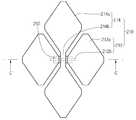
도 1은 일 실시예에 따른 터치 패널의 개략적인 평면도이다.
도 2는 일 실시예에 따른 터치 패널의 평면도이다.
도 3은 도 2의 A를 확대하여 도시한 평면도이다.
도 4는 도 3의 B-B'를 따라서 절단한 단면을 도시한 단면도이다.
도 5는 일 실시예에 따른 터치 패널의 단면도이다.
도 6은 일 실시예에 따른 터치 패널의 평면도이다.
도 7은 도 6의 C-C'를 따라서 절단한 단면을 도시한 단면도이다.
도 8은 일 실시예에 따른 터치 패널의 단면도이다.
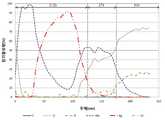
도 9는 비교예, 실시예 1 및 실시예 2의 파장에 따른 반사율을 비교한 그래프이다.
도 10은 실시예 1의 두께에 따른 원자함유량에 대한 그래프이다.
도 11은 실시예 2의 두께에 따른 원자함유량에 대한 그래프이다.1 is a schematic plan view of a touch panel according to an embodiment.
2 is a plan view of a touch panel according to an embodiment.
3 is a plan view showing an enlarged view of FIG. 2 A. FIG.
4 is a cross-sectional view showing a section taken along the line B-B 'in Fig.
5 is a cross-sectional view of a touch panel according to an embodiment.
6 is a plan view of a touch panel according to an embodiment.
7 is a cross-sectional view showing a section cut along the line C-C 'in Fig.
8 is a cross-sectional view of a touch panel according to an embodiment.
FIG. 9 is a graph comparing reflectivities according to wavelengths of Comparative Example, Example 1 and Example 2. FIG.
10 is a graph of atomic content according to the thickness of Example 1. Fig.
11 is a graph of atomic content according to the thickness of Example 2. Fig.
실시예들의 설명에 있어서, 각 층(막), 영역, 패턴 또는 구조물들이 기판, 각 층(막), 영역, 패드 또는 패턴들의 “상/위(on)”에 또는 “하/아래(under)”에 형성된다는 기재는, 직접(directly) 또는 다른 층을 개재하여 형성되는 것을 모두 포함한다. 각 층의 상/위 또는 하/아래에 대한 기준은 도면을 기준으로 설명한다.In the description of the embodiments, it is to be understood that each layer (film), area, pattern or structure may be referred to as being "on" or "under / under" Quot; includes all that is formed directly or through another layer. The criteria for top / bottom or bottom / bottom of each layer are described with reference to the drawings.
도면에서 각 층(막), 영역, 패턴 또는 구조물들의 두께나 크기는 설명의 명확성 및 편의를 위하여 변형될 수 있으므로, 실제 크기를 전적으로 반영하는 것은 아니다.The thickness or the size of each layer (film), region, pattern or structure in the drawings may be modified for clarity and convenience of explanation, and thus does not entirely reflect the actual size.
이하, 첨부한 도면을 참조하여 본 발명의 실시예를 상세하게 설명하면 다음과 같다.Hereinafter, embodiments of the present invention will be described in detail with reference to the accompanying drawings.
먼저, 도 1 내지 도 5를 참조하여, 일 실시예에 따른 터치 패널을 상세하게 설명한다. 도 1은 일 실시예에 따른 터치 패널의 개략적인 평면도이다. 도 2는 일 실시예에 따른 터치 패널의 평면도이다. 도 3은 도 2의 A를 확대하여 도시한 평면도이다. 도 4는 도 3의 B-B'를 따라서 절단한 단면을 도시한 단면도이다. 도 5는 일 실시예에 따른 터치 패널의 단면도이다.First, a touch panel according to an embodiment will be described in detail with reference to FIGS. 1 to 5. FIG. 1 is a schematic plan view of a touch panel according to an embodiment. 2 is a plan view of a touch panel according to an embodiment. 3 is a plan view showing an enlarged view of FIG. 2 A. FIG. 4 is a cross-sectional view showing a section taken along the line B-B 'in Fig. 5 is a cross-sectional view of a touch panel according to an embodiment.
도 1 및 도 2를 참조하면, 본 실시예에 따른 터치 패널은, 입력 장치(예를 들어, 손가락 등)의 위치를 감지하는 유효 영역(AA)과 이 유효 영역(AA)의 주위에 배치되는 비유효 영역(UA)이 정의되는 기판(100)을 포함한다.1 and 2, the touch panel according to the present embodiment includes a valid area AA for sensing the position of an input device (e.g., a finger or the like) And a
여기서 유효 영역(AA)에는 입력 장치를 감지할 수 있도록 투명 전극(210)이 형성될 수 있다. 그리고 비유효 영역(UA)에는 투명 전극(210)을 전기적으로 연결하는 배선(300)이 형성될 수 있다. 또한, 비유효 영역(UA)에는 배선(300)에 연결되는 외부 회로등이 위치할 수 있다. 이러한 비유효 영역(UA)에는 외곽 더미층(101)이 형성될 수 있으며, 이 외곽 더미층(101)에는 로고(logo)(102) 등이 형성될 수 있다.Here, the
이와 같은 터치 패널에 손가락 등의 입력 장치가 접촉되면, 입력 장치가 접촉된 부분에서 정전 용량의 차이가 발생되고, 이 차이가 발생된 부분을 접촉 위치로 검출할 수 있다.When such an input device such as a finger touches the touch panel, a difference in capacitance occurs at a portion where the input device is contacted, and a portion where the difference occurs can be detected as the contact position.
이러한 터치 패널을 좀더 상세하게 설명하면 다음과 같다.The touch panel will be described in more detail as follows.
기판(100)은 이 위에 형성되는 광흡수층(271), 투명 전극(210), 배선(300) 및 회로 기판 등을 지지할 수 있는 다양한 물질로 형성될 수 있다. 이러한 기판(100)은 일례로 유리 기판 또는 플라스틱 기판으로 이루어질 수 있다.The
기판(100)의 비유효 영역(UA)에 외곽 더미층(101)이 형성된다. 외곽 더미층(101)은 배선(300)과 이 배선(300)을 외부 회로에 연결하는 인쇄 회로 기판 등이 외부에서 보이지 않도록 할 수 있게 소정의 색을 가지는 물질을 도포하여 형성될 수 있다. 외곽 더미층(101)은 원하는 외관에 적합한 색을 가질 수 있는데, 일례로 흑색 안료 등을 포함하여 흑색을 나타낼 수 있다. 그리고 이 외곽 더미층(101)에는 다양한 방법으로 원하는 로고(102) 등을 형성할 수 있다. 이러한 외곽 더미층(101)은 증착, 인쇄, 습식 코팅 등에 의하여 형성될 수 있다.The
이어서, 기판(100) 상에는 투명 전극(210)이 형성될 수 있다. 상기 투명 전극(210)은 손가락 등의 입력 장치가 접촉되었는지 감지할 수 있다.Next, a
도 2 및 도 3을 참조하면, 상기 투명 전극(210)은 제1 전극(212) 및 제2 전극(214)을 포함한다.Referring to FIGS. 2 and 3, the
상기 제1 전극(212)은 손가락 등의 입력 장치가 접촉되었는지 감지하는 복수의 제1 센서부(212a)와, 이러한 복수의 제1 센서부(212a)를 연결하는 제1 연결전극부(212b)를 포함한다. 상기 제1 연결전극부(212b)는 상기 복수의 제1 센서부(212a)를 제1 방향(도면의 X축 방향)으로 연결하여, 상기 제1 전극(212)이 상기 제1 방향으로 연장될 수 있다.The
이와 유사하게, 상기 제2 전극(214)은 손가락 등의 입력 장치가 접촉되었는지 감지하는 복수의 제2 센서부(214a)와, 이러한 복수의 제2 센서부(214a)를 연결하는 제2 연결전극부(214b)를 포함한다. 상기 제2 연결전극부(214b)는 상기 복수의 제2 센서부(214a)를 상기 제1 방향과 교차하는 제2 방향(도면의 Y축 방향)으로 연결하여, 상기 제2 전극(214)이 상기 제2 방향으로 연장될 수 있다.Similarly, the
상기 제1 연결전극부(212b) 및 상기 제2 연결전극부(214b) 사이에는 전기적 단락을 방지하기 위한 절연층(250)이 위치할 수 있다. 상기 절연층(250)은 상기 제1 전극(212) 및 상기 제2 전극(214)을 절연할 수 있는 투명 절연성 물질을 포함할 수 있다.An
도 3을 참조하면, 기판(100) 상에 제1 센서부(212a), 제2 센서부(214a) 및 제2 연결전극부(214b)가 형성되고, 상기 제2 연결전극부(214b) 상에 절연층(250)이 형성된다. 상기 절연층(250) 상에 상기 제1 센서부(212a)를 연결하는 제1 연결전극부(212b)가 형성된다.3, a
한편, 도 4를 참조하면, 상기 제1 연결전극부(212b)는 두 개 이상의 층을 포함할 수 있다.Meanwhile, referring to FIG. 4, the first
구체적으로, 상기 제1 연결전극부(212b)는 버퍼층(212b1, 212b3) 및 전도층(212b2)을 포함할 수 있다. 상기 버퍼층(212b1, 212b3)은 제1 버퍼층(212b1) 및 제2 버퍼층(212b3)을 포함할 수 있다. 상기 제1 버퍼층(212b1) 및 상기 제2 버퍼층(212b3)은 상기 전도층(212b2)을 샌드위치할 수 있다. 즉, 상기 제1 버퍼층(212b1) 및 상기 제2 버퍼층(212b3)은 상기 전도층(212b2)을 사이에 두고 위치할 수 있다. 그러나 실시예가 이에 한정되는 것은 아니고, 상기 버퍼층은 한 층으로 구성되어 상기 전도층(212b2)의 상부 또는 하부에만 위치할 수 있다.Specifically, the first
상기 버퍼층(212b1, 212b3)은 상기 제1 연결전극부(212b) 및 상기 기판(100) 또는 상기 제1 연결전극부(212b) 및 상기 제1 센서부(212a)와의 밀착력을 향상시킬 수 있다. 상기 버퍼층(212b1, 212b3)은 전도성 금속을 포함할 수 있다. 구체적으로, 버퍼층(212b1, 212b3)은 Ni, Cr, Ni-Cr, Ti, Sn 또는 Mo 등의 물질을 증착하여 형성할 수 있다.The buffer layers 212b1 and 212b3 can improve adhesion between the first
상기 전도층(212b2)은 상기 제1 센서부(212a) 또는 제2 센서부(214a)보다 저항값이 낮은 전도성금속을 포함할 수 있다. 상기 전도층(212b2)은 Ag, Cu, Au, Mo 및 Al 등 전도성이 우수한 금속을 포함할 수 있다. 이러한 전도층(212b2)은 터치스크린의 감도에 직접적인 영향을 미치게 되므로, 저항값이 0.1Ω/□(square) 이하로 조절될 수 있도록, 증착 금속 및 두께를 조절할 수 있다.The conductive layer 212b2 may include a conductive metal having a resistance value lower than that of the
상기 기판(100) 상에 광흡수층(271)이 더 배치된다. 상기 광흡수층(271)은 상기 제1 연결전극부(212b)보다 상기 기판(100)에 더 인접하여 배치된다. 즉, 상기 광흡수층(271)은 상기 제1 연결전극부(212b)보다 상기 기판(100)과 더 가까이 위치한다. 따라서, 상기 광흡수층(271)은 상기 제1 연결전극부(212b)와 상기 기판(100) 사이에 위치한다.A
따라서, 상기 광흡수층(271)을 통해 상기 제1 연결전극부(212b)의 빛 반사에 의한 시인을 최소화할 수 있다. 즉, 상기 기판(100)으로 입사하는 입사광(I)을 상기 광흡수층(271)이 반사(R)시킴으로써, 상기 제1 연결전극부(212b)의 시인을 최소화할 수 있다.Therefore, the visibility due to light reflection of the first
특히, 실시예에 따른 터치 패널을 사용자가 사용할 때, 도 4에 도시한 바와 같이, 기판(100)의 센서부(212a), 제1 연결전극부(212b) 및 광흡수층(271) 등이 형성된 면(101)의 반대되는 면(102)에서 시인한다. 따라서, 상기 제1 연결전극부(212b)는 상기 반대되는 면(102)으로 입사하는 입사광(I)의 영향을 많이 받는데, 본 실시예에서는 상기 기판(100)과 상기 제1 연결전극부(212b) 사이에 광흡수층(271)이 배치됨으로써, 시인성을 감소시키는 효과가 크다.Particularly, when the user uses the touch panel according to the embodiment, as shown in FIG. 4, the
상기 광흡수층(271)은 전도성 금속의 산화물, 상기 전도성 금속의 질화물, 상기 전도성 금속의 탄화물 또는 이들의 혼합물을 포함할 수 있다. 이때, 상기 전도성 금속은 상기 버퍼층(212b1, 212b3)에 포함되는 전도성 금속과 대응될 수 있다. 따라서, 상기 전도성 금속은 Ni, Cr, Ni-Cr, Ti, Sn 또는 Mo 등의 물질을 포함할 수 있다.The
상기 광흡수층(271)은 전도성 금속, 산소, 질소 또는 탄소를 포함할 수 있다. 특히, 상기 산소, 질소 및 탄소는 선택적으로 포함될 수 있다. 즉, 상기 광흡수층(271)이 상기 전도성 금속의 산화물을 포함할 때, 상기 광흡수층(271)은 전도성 금속 및 산소를 포함할 수 있다. 또한, 상기 광흡수층(271)이 상기 전도성 금속의 질화물을 포함할 때, 상기 광흡수층(271)은 전도성 금속 및 질소를 포함할 수 있다. 상기 광흡수층(271)이 상기 전도성 금속의 탄화물을 포함할 때, 상기 광흡수층(271)은 전도성 금속 및 탄소를 포함할 수 있다.The
상기 전도성 금속은 상기 광흡수층(271) 내에서 상기 광흡수층(271)의 구성 물질 전체 중량에 대하여 35 % 내지 50 % 포함될 수 있다. 상기 산소는 상기 광흡수층(271) 내에서 상기 광흡수층(271)의 구성 물질 전체 중량에 대하여 30 % 내지 40 % 포함될 수 있다. 상기 질소는 상기 광흡수층(271) 내에서 상기 광흡수층(271)의 구성 물질 전체 중량에 대하여 0 % 내지 10 % 포함될 수 있다. 상기 탄소는 상기 광흡수층(271) 내에서 상기 광흡수층(271)의 구성 물질 전체 중량에 대하여 0 % 내지 5 % 포함될 수 있다. 상기 전도성 금속, 산소, 질소 또는 탄소의 원자함유량 및 광흡수층(271)의 두께에 따라 상기 광흡수층(271)의 평균 반사율이 조절될 수 있다. 구체적으로, 상기 광흡수층(271)은 전도성 금속, Ar, N2 또는 CO2 가스를 이용하여 반응성 스퍼터링으로 형성될 수 있는데 이때, 반응성 스퍼터링에 사용되는 가스량(분압비) 조절을 통해 반사율을 최적화할 수 있다. 이를 통해, 상기 광흡수층(271)의 가시광영역인 380 nm 내지 780 nm의 파장에서 평균 반사율을 5 % 내지 10 % 로 조절할 수 있다.The conductive metal may include 35% to 50% of the total weight of the
한편, 도 5를 참조하면, 상기 광흡수층(271, 272)은 제1 광흡수층(271) 및 제2 광흡수층(272)을 포함할 수 있다. 상기 제1 광흡수층(271) 및 상기 제2 광흡수층(272)은 상기 제1 연결전극부(212b)를 샌드위치할 수 있다. 즉, 상기 제1 광흡수층(271) 및 상기 제2 광흡수층(272)은 상기 제1 연결전극부(212b)를 사이에 두고 배치될 수 있다. 상기 제1 연결전극부(212b)의 상부 및 하부에 각각 상기 제1 광흡수층(271) 및 제2 광흡수층(272)이 배치됨으로써, 빛 반사를 극대화할 수 있다.Referring to FIG. 5, the
이어서, 상기 배선(300)은 상기 비유효 영역(UA)에 형성된다. 상기 배선(300)은 상기 투명 전극(210)에 전기적 신호를 인가할 수 있다. 도면에 도시하지 않았으나, 상기 배선(300) 상에 광흡수층이 배치될 수 있다. 구체적으로, 상기 광흡수층은 상기 배선(300)보다 상기 기판에 더 인접하여 배치될 수 있다. 상기 광흡수층(271)은 상기 배선(300)의 하부에 배치될 수 있다. 상기 광흡수층(271)은 상기 기판(100)과 직접 접촉할 수 있다. 또한, 상기 광흡수층(271)은 제1 광흡수층(271) 및 제2 광흡수층(272)을 포함할 수 있다. 상기 제1 광흡수층(271) 및 상기 제2 광흡수층(272)은 상기 배선(300)을 샌드위치할 수 있다.Subsequently, the
상기 배선(300)은 상기 비유효 영역(UA)에 형성되어 보이지 않게 할 수 있다.The
한편, 도면에 도시하지 않았으나, 상기 배선(300)과 연결되는 회로 기판이 더 위치할 수 있다. 회로 기판으로는 다양한 형태의 인쇄 회로 기판(100)이 적용될 수 있는데, 일례로 플렉서블 인쇄 회로 기판(flexible printed circuit board, FPCB) 등이 적용될 수 있다.Meanwhile, although not shown in the drawing, a circuit board connected to the
이하, 도 6 내지 도 8을 참조하여, 다른 실시예에 따른 터치 패널을 상세하게 설명한다. 도 6은 일 실시예에 따른 터치 패널의 평면도이다. 도 7은 도 6의 C-C'를 따라서 절단한 단면을 도시한 단면도이다. 도 8은 일 실시예에 따른 터치 패널의 단면도이다.Hereinafter, a touch panel according to another embodiment will be described in detail with reference to FIGS. 6 to 8. FIG. 6 is a plan view of a touch panel according to an embodiment. 7 is a cross-sectional view showing a section cut along the line C-C 'in Fig. 8 is a cross-sectional view of a touch panel according to an embodiment.
먼저, 도 6 및 도 7을 참조하면, 상기 기판(100) 상에 광흡수층(271)이 위치한다. 즉, 상기 광흡수층(271)은 상기 기판(100)과 직접 접촉한다. 상기 광흡수층(271) 상에 제1 연결전극부(212b)가 배치된다. 상기 제1 연결전극부(212b) 상에 절연층(250)이 배치되며, 상기 절연층(250) 상에 제2 연결전극부(214b)가 차례대로 배치될 수 있다. 상기 광흡수층(271)이 상기 기판(100)과 직접 접촉함으로써, 상기 기판(100)으로 입사하는 입사광을 보다 효과적으로 반사시킬 수 있다. 따라서, 상기 제1 연결전극부(212b)의 시인성을 최소화할 수 있다.6 and 7, a
또한, 도 8을 참조하면, 상기 광흡수층(271, 272)은 제1 광흡수층(271) 및 제2 광흡수층(272)을 포함하고, 상기 제1 광흡수층(271) 및 제2 광흡수층(272)은 상기 제1 연결전극부(212b)를 샌드위치할 수 있다.
8, the
이하, 실시예를 통하여 본 발명을 좀더 상세하게 설명하고자 한다. 그러나 실시예는 본 발명을 예시하기 위한 것에 불과하며, 본 발명이 이에 한정되는 것은 아니다.
Hereinafter, the present invention will be described in more detail by way of examples. However, the present invention is not limited thereto.
실시예Example 1 One
유리 기판 상에 인듐 주석 산화물(indium tin oxide, ITO)을 증착하여 센서부를 형성하였다. 상기 센서부 상에 절연층을 형성하였다. 상기 절연층 상에 Mo, Ar, N2 및 CO2 가스를 반응성 스퍼터링을 통해 증착하여 제1 광흡수층을 형성하였다. 따라서, 제1 광흡수층은 질화물과 산화물의 혼합물을 포함한다. 상기 제1 광흡수층 상에 Mo를 포함하는 제1 버퍼층, Ag를 포함하는 전도층 및 Mo를 포함하는 제2 버퍼층을 형성하여 제1 버퍼층, 전도층 및 제2 버퍼층을 포함하는 연결 전극을 형성하였다.
Indium tin oxide (ITO) was deposited on the glass substrate to form a sensor portion. An insulating layer was formed on the sensor portion. Mo, Ar, N2, and CO2 gases were deposited on the insulating layer through reactive sputtering to form a first light absorbing layer. Thus, the first light absorbing layer comprises a mixture of nitride and oxide. A first buffer layer containing Mo, a conductive layer containing Ag, and a second buffer layer containing Mo were formed on the first light absorption layer to form a connection electrode including a first buffer layer, a conductive layer and a second buffer layer .
실시예Example 2 2
연결 전극 상에 상기 제1 광흡수층을 형성하는 방법과 동일한 방법으로 제2 광흡수층을 더 형성하였다는 점을 제외하고, 실시예 1과 동일한 방법으로 터치 패널을 제조하였다.
A touch panel was manufactured in the same manner as in Example 1 except that a second light absorbing layer was further formed in the same manner as the method of forming the first light absorbing layer on the connecting electrode.
비교예Comparative Example
제1 광흡수층은 형성하지 않았다는 점을 제외하고, 실시예 1과 동일한 방법으로 터치 패널을 제조하였다.
A touch panel was manufactured in the same manner as in Example 1, except that the first light absorbing layer was not formed.
도 9를 참조하면, 비교예의 경우 가시광영역인 380 nm 내지 780 nm의 파장에서 평균 반사율이 약 52 % 이었다. 한편, 실시예 1 및 실시예 2의 경우 가시광영역의 파장에서 평균 반사율이 각각 약 7.4 % 및 약 7.9 %로 비교예에 비해 매우 낮은 반사율을 나타내었다.Referring to FIG. 9, in the comparative example, the average reflectance was about 52% at a wavelength of 380 nm to 780 nm, which is a visible light region. On the other hand, in Examples 1 and 2, the average reflectance at the wavelength of the visible light region was about 7.4% and about 7.9%, respectively.
한편, 도 10은 실시예 1의 두께에 따른 원자함유량에 대한 그래프이다. 도 11은 실시예 2의 두께에 따른 원자함유량에 대한 그래프이다. 실시예 1 및 실시예 2의 원자함유량이 각각 도 10 및 도 11을 만족함에 따라, 상기와 같은 낮은 평균 반사율을 만족할 수 있다.FIG. 10 is a graph showing the atomic content according to the thickness of Example 1. FIG. 11 is a graph of atomic content according to the thickness of Example 2. Fig. When the atomic contents of Examples 1 and 2 satisfy the conditions shown in Figs. 10 and 11, the low average reflectance as described above can be satisfied.
상술한 실시예에 설명된 특징, 구조, 효과 등은 본 발명의 적어도 하나의 실시예에 포함되며, 반드시 하나의 실시예에만 한정되는 것은 아니다. 나아가, 각 실시예에서 예시된 특징, 구조, 효과 등은 실시예들이 속하는 분야의 통상의 지식을 가지는 자에 의하여 다른 실시예들에 대해서도 조합 또는 변형되어 실시 가능하다. 따라서 이러한 조합과 변형에 관계된 내용들은 본 발명의 범위에 포함되는 것으로 해석되어야 할 것이다.The features, structures, effects and the like described in the foregoing embodiments are included in at least one embodiment of the present invention and are not necessarily limited to one embodiment. Further, the features, structures, effects, and the like illustrated in the embodiments may be combined or modified in other embodiments by those skilled in the art to which the embodiments belong. Therefore, it should be understood that the present invention is not limited to these combinations and modifications.
또한, 이상에서 실시예들을 중심으로 설명하였으나 이는 단지 예시일 뿐 본 발명을 한정하는 것이 아니며, 본 발명이 속하는 분야의 통상의 지식을 가진 자라면 본 실시예의 본질적인 특성을 벗어나지 않는 범위에서 이상에 예시되지 않은 여러 가지의 변형과 응용이 가능함을 알 수 있을 것이다. 예를 들어, 실시예들에 구체적으로 나타난 각 구성 요소는 변형하여 실시할 수 있는 것이다. 그리고 이러한 변형과 응용에 관계된 차이점들은 첨부한 청구 범위에서 규정하는 본 발명의 범위에 포함되는 것으로 해석되어야 할 것이다.While the present invention has been particularly shown and described with reference to exemplary embodiments thereof, it is clearly understood that the same is by way of illustration and example only and is not to be construed as limiting the scope of the present invention. It can be seen that various modifications and applications are possible. For example, each component specifically shown in the embodiments may be modified and implemented. It is to be understood that the present invention may be embodied in many other specific forms without departing from the spirit or essential characteristics thereof.
Claims (19)
Translated fromKorean상기 기판 상에 배치되는 제 1 전극; 및 상기 제 1 전극과 이격하여 배치되는 제 2 전극;
상기 제 1 전극 및 상기 제 2 전극을 절연하는 절연층;
상기 기판 상에 배치되고, 상기 제 2 전극을 연결하는 연결 전극; 및
상기 기판 상에 배치되는 광흡수층을 포함하고,
상기 제 1 전극 및 상기 제 2 전극은 상기 기판의 동일 면 상에 배치되고,
상기 광흡수층은,
상기 연결 전극의 하부에 배치되는 제1 광흡수층; 및
상기 연결 전극의 상부에 배치되는 제2 광흡수층을 포함하고,
상기 제1 광흡수층 및 상기 제2 광흡수층은 상기 연결 전극을 샌드위치하며 배치되고,
상기 광흡수층은 전도성 금속의 산화물, 전도성 금속의 질화물, 전도성 금속의 탄화물 및 이들의 혼합물로 이루어진 군에서 선택된 물질 중 어느 하나를 포함하는 터치 패널.Board;
A first electrode disposed on the substrate; And a second electrode spaced apart from the first electrode;
An insulating layer for insulating the first electrode and the second electrode;
A connection electrode disposed on the substrate and connecting the second electrode; And
And a light absorbing layer disposed on the substrate,
Wherein the first electrode and the second electrode are disposed on the same side of the substrate,
The light-
A first light absorbing layer disposed under the connection electrode; And
And a second light absorbing layer disposed on the connection electrode,
Wherein the first light absorbing layer and the second light absorbing layer sandwich the connection electrode,
Wherein the light absorbing layer comprises any one selected from the group consisting of an oxide of a conductive metal, a nitride of a conductive metal, a carbide of a conductive metal, and a mixture thereof.
상기 전도성 금속은 상기 광흡수층의 구성 물질 전체에 대하여 35 % 내지 50 % 포함되는 터치 패널.The method according to claim 1,
Wherein the conductive metal comprises 35% to 50% of the total constituent materials of the light absorbing layer.
상기 광 흡수층은 전도성 금속 및 산소를 포함하고,
상기 산소는 상기 광흡수층의 구성 물질 전체에 대하여 30 % 내지 40 % 포함되는 터치 패널.The method according to claim 1,
Wherein the light absorbing layer comprises a conductive metal and oxygen,
Wherein the oxygen comprises 30% to 40% of the total constituent materials of the light absorbing layer.
상기 광 흡수층은 전도성 금속 및 질소를 포함하고,
상기 질소는 상기 광흡수층의 구성 물질 전체에 대하여 0 % 내지 10 % 포함되는 터치 패널.The method according to claim 1,
Wherein the light absorbing layer comprises a conductive metal and nitrogen,
Wherein the nitrogen includes 0% to 10% of the total constituent materials of the light absorbing layer.
상기 광 흡수층은 전도성 금속 및 탄소를 포함하고,
상기 탄소는 상기 광흡수층의 구성 물질 전체에 대하여 0 % 내지 5 % 포함되는 터치 패널.The method according to claim 1,
Wherein the light absorbing layer comprises a conductive metal and carbon,
Wherein the carbon comprises 0% to 5% of the total constituent materials of the light absorbing layer.
상기 광흡수층은 상기 기판과 직접 접촉하며 배치되는 터치 패널.The method according to claim 1,
Wherein the light absorbing layer is disposed in direct contact with the substrate.
상기 연결 전극은 전도층; 및 상기 전도층의 적어도 일면 상에 배치되는 버퍼층을 포함하는 터치 패널.The method according to claim 1,
The connection electrode comprises a conductive layer; And a buffer layer disposed on at least one surface of the conductive layer.
상기 버퍼층은 전도성 금속을 포함하는 터치 패널.8. The method of claim 7,
Wherein the buffer layer comprises a conductive metal.
상기 버퍼층은 Ni, Cr, Ni-Cr, Ti, Sn 및 Mo으로 이루어진 군에서 선택된 물질을 어느 하나 포함하는 터치 패널.8. The method of claim 7,
Wherein the buffer layer comprises any one selected from the group consisting of Ni, Cr, Ni-Cr, Ti, Sn and Mo.
상기 버퍼층은,
상기 전도층의 일면 상에 배치되는 제1 버퍼층; 및
상기 전도층의 일면과 반대되는 타면 상에 배치되는 제2 버퍼층을 포함하는 터치 패널.8. The method of claim 7,
The buffer layer may be formed,
A first buffer layer disposed on one surface of the conductive layer; And
And a second buffer layer disposed on the other surface opposite to the one surface of the conductive layer.
상기 제1 버퍼층 및 상기 제2 버퍼층은 상기 전도층을 샌드위치하는 터치 패널.11. The method of claim 10,
Wherein the first buffer layer and the second buffer layer sandwich the conductive layer.
상기 제 1 전극 및 상기 제 2 전극을 전기적으로 연결하는 배선을 더 포함하고,
상기 배선 상에 배치되는 광흡수층을 포함하며,
상기 광흡수층은 상기 배선보다 상기 기판에 더 인접하여 배치된 부분을 포함하는 터치 패널.The method according to claim 1,
Further comprising a wiring electrically connecting the first electrode and the second electrode,
And a light absorbing layer disposed on the wiring,
Wherein the light absorption layer includes a portion disposed closer to the substrate than the wiring.
상기 기판 상에 배치되는 제 1 전극; 및 상기 제 1 전극과 이격하여 배치되는 제 2 전극을 형성하는 단계;
상기 제 1 전극 및 상기 제 2 전극을 절연하는 절연층을 형성하는 단계;
상기 기판 상에 배치되고, 상기 제 2 전극을 연결하는 연결 전극을 형성하는 단계; 및
상기 기판 상에 광흡수층을 형성하는 단계를 포함하고,
상기 광흡수층은,
상기 연결 전극의 하부에 배치되는 제1 광흡수층; 및
상기 연결 전극의 상부에 배치되는 제2 광흡수층을 포함하고,
상기 제1 광흡수층 및 상기 제2 광흡수층은 상기 연결 전극을 샌드위치하며 배치되고,
상기 광흡수층은 전도성 금속의 산화물, 전도성 금속의 질화물, 전도성 금속의 탄화물 및 이들의 혼합물로 이루어진 군에서 선택된 물질 중 어느 하나를 포함하는 터치 패널의 제조방법.Preparing a substrate;
A first electrode disposed on the substrate; And forming a second electrode spaced apart from the first electrode;
Forming an insulating layer insulating the first electrode and the second electrode;
Forming a connection electrode on the substrate, the connection electrode connecting the second electrode; And
And forming a light absorbing layer on the substrate,
The light-
A first light absorbing layer disposed under the connection electrode; And
And a second light absorbing layer disposed on the connection electrode,
Wherein the first light absorbing layer and the second light absorbing layer sandwich the connection electrode,
Wherein the light absorbing layer comprises any one selected from the group consisting of an oxide of a conductive metal, a nitride of a conductive metal, a carbide of a conductive metal, and a mixture thereof.
상기 광흡수층을 형성하는 단계에서는 전도성 금속, Ar, N2 및 CO2 로 이루어진 군에서 선택된 물질을 이용하여 증착하는 터치 패널의 제조방법.14. The method of claim 13,
Wherein the light absorption layer is formed using a material selected from the group consisting of a conductive metal, Ar, N2, and CO2 .
Priority Applications (5)
| Application Number | Priority Date | Filing Date | Title |
|---|---|---|---|
| KR1020120113201AKR101976637B1 (en) | 2012-10-11 | 2012-10-11 | Touch panel and method for manufacturing the same |
| US14/419,815US9891656B2 (en) | 2012-10-11 | 2013-04-02 | Touch panel and method for manufacturing the same |
| CN201380042069.4ACN104520791B (en) | 2012-10-11 | 2013-04-02 | Touch pad and the method for manufacturing the touch pad |
| PCT/KR2013/002721WO2014058116A1 (en) | 2012-10-11 | 2013-04-02 | Touch panel and method for manufacturing the same |
| TW102113983ATWI613571B (en) | 2012-10-11 | 2013-04-19 | Touch panel and method for manufacturing the same |
Applications Claiming Priority (1)
| Application Number | Priority Date | Filing Date | Title |
|---|---|---|---|
| KR1020120113201AKR101976637B1 (en) | 2012-10-11 | 2012-10-11 | Touch panel and method for manufacturing the same |
Related Child Applications (1)
| Application Number | Title | Priority Date | Filing Date |
|---|---|---|---|
| KR1020190047885ADivisionKR102008725B1 (en) | 2019-04-24 | 2019-04-24 | Touch panel and method for manufacturing the same |
Publications (2)
| Publication Number | Publication Date |
|---|---|
| KR20140046944A KR20140046944A (en) | 2014-04-21 |
| KR101976637B1true KR101976637B1 (en) | 2019-05-10 |
Family
ID=50477565
Family Applications (1)
| Application Number | Title | Priority Date | Filing Date |
|---|---|---|---|
| KR1020120113201AActiveKR101976637B1 (en) | 2012-10-11 | 2012-10-11 | Touch panel and method for manufacturing the same |
Country Status (5)
| Country | Link |
|---|---|
| US (1) | US9891656B2 (en) |
| KR (1) | KR101976637B1 (en) |
| CN (1) | CN104520791B (en) |
| TW (1) | TWI613571B (en) |
| WO (1) | WO2014058116A1 (en) |
Families Citing this family (12)
| Publication number | Priority date | Publication date | Assignee | Title |
|---|---|---|---|---|
| KR101926602B1 (en)* | 2012-05-31 | 2018-12-11 | 엘지이노텍 주식회사 | Touch panel and manufacturing method thereof |
| US10372279B2 (en) | 2014-08-14 | 2019-08-06 | Lg Innotek Co., Ltd. | Touch window |
| US10349511B2 (en)* | 2015-02-10 | 2019-07-09 | Lg Chem, Ltd. | Conductive structure and manufacturing method thereof |
| US20180067581A1 (en)* | 2015-03-25 | 2018-03-08 | Lg Chem, Ltd. | Conductive structure and manufacturing method therefor |
| KR101947604B1 (en)* | 2015-03-25 | 2019-02-14 | 주식회사 엘지화학 | Conductive structure body and method for manufacturing the same |
| KR101977852B1 (en)* | 2015-06-03 | 2019-05-13 | 주식회사 엘지화학 | Conductive structure body and method for manufacturing the same |
| KR101997661B1 (en) | 2015-10-27 | 2019-07-08 | 주식회사 엘지화학 | Conductive structure body, electrode and display device comprising the same |
| KR102426951B1 (en)* | 2015-11-06 | 2022-07-29 | 엘지이노텍 주식회사 | Sensing apparatus which dummy pattern formed |
| KR20170067592A (en)* | 2015-12-08 | 2017-06-16 | 주식회사 엘지화학 | Touch panel and method for manufacturing the same |
| KR101913394B1 (en) | 2016-07-29 | 2018-10-31 | 삼성디스플레이 주식회사 | Display device |
| CN106886338B (en)* | 2017-02-08 | 2023-03-10 | 江西卓讯微电子有限公司 | Touch screen and electronic device |
| KR102374754B1 (en)* | 2017-09-27 | 2022-03-15 | 엘지디스플레이 주식회사 | Display device having a touch structure |
Family Cites Families (15)
| Publication number | Priority date | Publication date | Assignee | Title |
|---|---|---|---|---|
| JP2003296032A (en) | 2002-04-03 | 2003-10-17 | Pioneer Electronic Corp | Display integrated touch panel device and method of manufacturing the same |
| TWI480676B (en)* | 2004-03-31 | 2015-04-11 | Shinetsu Chemical Co | Halftone phase shift blank mask, halftone phase shift mask, and pattern transfer method |
| JP5116004B2 (en)* | 2006-08-03 | 2013-01-09 | 日東電工株式会社 | Transparent conductive laminate and touch panel provided with the same |
| JP5060845B2 (en)* | 2007-06-27 | 2012-10-31 | 株式会社ジャパンディスプレイイースト | Screen input type image display device |
| CN101452351B (en)* | 2007-12-03 | 2010-11-17 | 义强科技股份有限公司 | Touch device with high light transmittance |
| KR101172113B1 (en)* | 2008-11-14 | 2012-08-10 | 엘지이노텍 주식회사 | Touch screen and method of manufactureing the same |
| CN101989160A (en)* | 2009-08-07 | 2011-03-23 | 铼宝科技股份有限公司 | Capacitive touch panel |
| KR101144152B1 (en)* | 2009-11-17 | 2012-05-09 | (주)삼원에스티 | Touch panel sensor |
| KR20120032734A (en) | 2010-09-29 | 2012-04-06 | 삼성모바일디스플레이주식회사 | Touch screen panel and fabricating method thereof |
| CN103168285B (en) | 2010-10-19 | 2016-05-11 | Lg化学株式会社 | Touch panel including conductive pattern and manufacturing method thereof |
| CN102566842B (en) | 2010-12-06 | 2014-10-29 | 乐金显示有限公司 | Electrostatic capacity type touch screen panel |
| GB2487962B (en) | 2011-02-11 | 2016-10-12 | M-Solv Ltd | Method for making a two-layer capacitive touch sensor panel |
| JP2013012020A (en)* | 2011-06-29 | 2013-01-17 | Panasonic Corp | Touch panel |
| CN102929454A (en) | 2011-08-12 | 2013-02-13 | 宸鸿科技(厦门)有限公司 | Capacitive touch panel and method for reducing visibility of metal conductors thereof |
| TWM432091U (en) | 2012-01-11 | 2012-06-21 | Henghao Technology Co Ltd | Capacitive touch panel and touch display panel using the same |
- 2012
- 2012-10-11KRKR1020120113201Apatent/KR101976637B1/enactiveActive
- 2013
- 2013-04-02CNCN201380042069.4Apatent/CN104520791B/enactiveActive
- 2013-04-02USUS14/419,815patent/US9891656B2/enactiveActive
- 2013-04-02WOPCT/KR2013/002721patent/WO2014058116A1/enactiveApplication Filing
- 2013-04-19TWTW102113983Apatent/TWI613571B/enactive
Also Published As
| Publication number | Publication date |
|---|---|
| TW201415322A (en) | 2014-04-16 |
| TWI613571B (en) | 2018-02-01 |
| KR20140046944A (en) | 2014-04-21 |
| US9891656B2 (en) | 2018-02-13 |
| US20150212539A1 (en) | 2015-07-30 |
| WO2014058116A1 (en) | 2014-04-17 |
| CN104520791B (en) | 2018-05-08 |
| CN104520791A (en) | 2015-04-15 |
Similar Documents
| Publication | Publication Date | Title |
|---|---|---|
| KR101976637B1 (en) | Touch panel and method for manufacturing the same | |
| US10592043B2 (en) | Touch panel and method for manufacturing the same | |
| EP2652583B1 (en) | Touch panel, method for manufacturing the same, and liquid crystal display device including the touch panel | |
| KR102388979B1 (en) | Touch sensor arrangement | |
| US20100328248A1 (en) | Capacitive touch screen with reduced electrode trace resistance | |
| US20130194220A1 (en) | Touch panel | |
| KR102255445B1 (en) | Touch sensor | |
| KR101931179B1 (en) | Touch panel and method for manufacturing the same | |
| KR101865685B1 (en) | Transparent electrode pattern structure and touch screen panel having the same | |
| TWI584180B (en) | Transparent electrode pattern structure and touch screen panel having the same | |
| KR101049016B1 (en) | Touch screen panel and its manufacturing method | |
| KR101181056B1 (en) | Touch panel | |
| KR102077548B1 (en) | Transparent electrode pattern structure and touch screen panel having the same | |
| KR102027775B1 (en) | Touch sensor | |
| JP2008135291A (en) | Touch panel and its manufacturing method | |
| KR102008725B1 (en) | Touch panel and method for manufacturing the same | |
| KR101114024B1 (en) | Touch panel | |
| KR20150084545A (en) | Touch panel |
Legal Events
| Date | Code | Title | Description |
|---|---|---|---|
| PA0109 | Patent application | Patent event code:PA01091R01D Comment text:Patent Application Patent event date:20121011 | |
| PG1501 | Laying open of application | ||
| PA0201 | Request for examination | Patent event code:PA02012R01D Patent event date:20170926 Comment text:Request for Examination of Application Patent event code:PA02011R01I Patent event date:20121011 Comment text:Patent Application | |
| E902 | Notification of reason for refusal | ||
| PE0902 | Notice of grounds for rejection | Comment text:Notification of reason for refusal Patent event date:20181119 Patent event code:PE09021S01D | |
| E701 | Decision to grant or registration of patent right | ||
| PE0701 | Decision of registration | Patent event code:PE07011S01D Comment text:Decision to Grant Registration Patent event date:20190326 | |
| A107 | Divisional application of patent | ||
| PA0107 | Divisional application | Comment text:Divisional Application of Patent Patent event date:20190424 Patent event code:PA01071R01D | |
| PR0701 | Registration of establishment | Comment text:Registration of Establishment Patent event date:20190502 Patent event code:PR07011E01D | |
| PR1002 | Payment of registration fee | Payment date:20190503 End annual number:3 Start annual number:1 | |
| PG1601 | Publication of registration | ||
| PR1001 | Payment of annual fee | Payment date:20220413 Start annual number:4 End annual number:4 | |
| PR1001 | Payment of annual fee | Payment date:20230412 Start annual number:5 End annual number:5 | |
| PR1001 | Payment of annual fee | Payment date:20240415 Start annual number:6 End annual number:6 | |
| PR1001 | Payment of annual fee | Payment date:20250415 Start annual number:7 End annual number:7 |