KR101976212B1 - Semiconductor device and method for manufacturing the same - Google Patents
Semiconductor device and method for manufacturing the sameDownload PDFInfo
- Publication number
- KR101976212B1 KR101976212B1KR1020120113434AKR20120113434AKR101976212B1KR 101976212 B1KR101976212 B1KR 101976212B1KR 1020120113434 AKR1020120113434 AKR 1020120113434AKR 20120113434 AKR20120113434 AKR 20120113434AKR 101976212 B1KR101976212 B1KR 101976212B1
- Authority
- KR
- South Korea
- Prior art keywords
- film
- oxide semiconductor
- electrode layer
- semiconductor film
- transistor
- Prior art date
- Legal status (The legal status is an assumption and is not a legal conclusion. Google has not performed a legal analysis and makes no representation as to the accuracy of the status listed.)
- Expired - Fee Related
Links
Images


Classifications
- H—ELECTRICITY
- H10—SEMICONDUCTOR DEVICES; ELECTRIC SOLID-STATE DEVICES NOT OTHERWISE PROVIDED FOR
- H10D—INORGANIC ELECTRIC SEMICONDUCTOR DEVICES
- H10D84/00—Integrated devices formed in or on semiconductor substrates that comprise only semiconducting layers, e.g. on Si wafers or on GaAs-on-Si wafers
- H10D84/01—Manufacture or treatment
- H—ELECTRICITY
- H10—SEMICONDUCTOR DEVICES; ELECTRIC SOLID-STATE DEVICES NOT OTHERWISE PROVIDED FOR
- H10D—INORGANIC ELECTRIC SEMICONDUCTOR DEVICES
- H10D30/00—Field-effect transistors [FET]
- H10D30/60—Insulated-gate field-effect transistors [IGFET]
- H10D30/67—Thin-film transistors [TFT]
- H10D30/674—Thin-film transistors [TFT] characterised by the active materials
- H10D30/6755—Oxide semiconductors, e.g. zinc oxide, copper aluminium oxide or cadmium stannate
- H10D30/6756—Amorphous oxide semiconductors
- H—ELECTRICITY
- H10—SEMICONDUCTOR DEVICES; ELECTRIC SOLID-STATE DEVICES NOT OTHERWISE PROVIDED FOR
- H10D—INORGANIC ELECTRIC SEMICONDUCTOR DEVICES
- H10D30/00—Field-effect transistors [FET]
- H10D30/60—Insulated-gate field-effect transistors [IGFET]
- H10D30/67—Thin-film transistors [TFT]
- H10D30/674—Thin-film transistors [TFT] characterised by the active materials
- H10D30/6755—Oxide semiconductors, e.g. zinc oxide, copper aluminium oxide or cadmium stannate
- H—ELECTRICITY
- H01—ELECTRIC ELEMENTS
- H01L—SEMICONDUCTOR DEVICES NOT COVERED BY CLASS H10
- H01L21/00—Processes or apparatus adapted for the manufacture or treatment of semiconductor or solid state devices or of parts thereof
- H01L21/02—Manufacture or treatment of semiconductor devices or of parts thereof
- H01L21/02041—Cleaning
- H01L21/02057—Cleaning during device manufacture
- H01L21/02068—Cleaning during device manufacture during, before or after processing of conductive layers, e.g. polysilicon or amorphous silicon layers
- H01L21/02071—Cleaning during device manufacture during, before or after processing of conductive layers, e.g. polysilicon or amorphous silicon layers the processing being a delineation, e.g. RIE, of conductive layers
- H—ELECTRICITY
- H01—ELECTRIC ELEMENTS
- H01L—SEMICONDUCTOR DEVICES NOT COVERED BY CLASS H10
- H01L21/00—Processes or apparatus adapted for the manufacture or treatment of semiconductor or solid state devices or of parts thereof
- H01L21/02—Manufacture or treatment of semiconductor devices or of parts thereof
- H01L21/04—Manufacture or treatment of semiconductor devices or of parts thereof the devices having potential barriers, e.g. a PN junction, depletion layer or carrier concentration layer
- H01L21/18—Manufacture or treatment of semiconductor devices or of parts thereof the devices having potential barriers, e.g. a PN junction, depletion layer or carrier concentration layer the devices having semiconductor bodies comprising elements of Group IV of the Periodic Table or AIIIBV compounds with or without impurities, e.g. doping materials
- H01L21/28—Manufacture of electrodes on semiconductor bodies using processes or apparatus not provided for in groups H01L21/20 - H01L21/268
- H—ELECTRICITY
- H01—ELECTRIC ELEMENTS
- H01L—SEMICONDUCTOR DEVICES NOT COVERED BY CLASS H10
- H01L21/00—Processes or apparatus adapted for the manufacture or treatment of semiconductor or solid state devices or of parts thereof
- H01L21/02—Manufacture or treatment of semiconductor devices or of parts thereof
- H01L21/04—Manufacture or treatment of semiconductor devices or of parts thereof the devices having potential barriers, e.g. a PN junction, depletion layer or carrier concentration layer
- H01L21/18—Manufacture or treatment of semiconductor devices or of parts thereof the devices having potential barriers, e.g. a PN junction, depletion layer or carrier concentration layer the devices having semiconductor bodies comprising elements of Group IV of the Periodic Table or AIIIBV compounds with or without impurities, e.g. doping materials
- H01L21/30—Treatment of semiconductor bodies using processes or apparatus not provided for in groups H01L21/20 - H01L21/26
- H01L21/31—Treatment of semiconductor bodies using processes or apparatus not provided for in groups H01L21/20 - H01L21/26 to form insulating layers thereon, e.g. for masking or by using photolithographic techniques; After treatment of these layers; Selection of materials for these layers
- H01L21/3205—Deposition of non-insulating-, e.g. conductive- or resistive-, layers on insulating layers; After-treatment of these layers
- H01L21/321—After treatment
- H01L21/3213—Physical or chemical etching of the layers, e.g. to produce a patterned layer from a pre-deposited extensive layer
- H01L21/32133—Physical or chemical etching of the layers, e.g. to produce a patterned layer from a pre-deposited extensive layer by chemical means only
- H01L21/32135—Physical or chemical etching of the layers, e.g. to produce a patterned layer from a pre-deposited extensive layer by chemical means only by vapour etching only
- H01L21/32136—Physical or chemical etching of the layers, e.g. to produce a patterned layer from a pre-deposited extensive layer by chemical means only by vapour etching only using plasmas
- H—ELECTRICITY
- H01—ELECTRIC ELEMENTS
- H01L—SEMICONDUCTOR DEVICES NOT COVERED BY CLASS H10
- H01L21/00—Processes or apparatus adapted for the manufacture or treatment of semiconductor or solid state devices or of parts thereof
- H01L21/02—Manufacture or treatment of semiconductor devices or of parts thereof
- H01L21/04—Manufacture or treatment of semiconductor devices or of parts thereof the devices having potential barriers, e.g. a PN junction, depletion layer or carrier concentration layer
- H01L21/34—Manufacture or treatment of semiconductor devices or of parts thereof the devices having potential barriers, e.g. a PN junction, depletion layer or carrier concentration layer the devices having semiconductor bodies not provided for in groups H01L21/18, H10D48/04 and H10D48/07, with or without impurities, e.g. doping materials
- H01L21/46—Treatment of semiconductor bodies using processes or apparatus not provided for in groups H01L21/428
- H01L21/461—Treatment of semiconductor bodies using processes or apparatus not provided for in groups H01L21/428 to change their surface-physical characteristics or shape, e.g. etching, polishing, cutting
- H01L21/465—Chemical or electrical treatment, e.g. electrolytic etching
- H—ELECTRICITY
- H10—SEMICONDUCTOR DEVICES; ELECTRIC SOLID-STATE DEVICES NOT OTHERWISE PROVIDED FOR
- H10D—INORGANIC ELECTRIC SEMICONDUCTOR DEVICES
- H10D30/00—Field-effect transistors [FET]
- H10D30/01—Manufacture or treatment
- H—ELECTRICITY
- H10—SEMICONDUCTOR DEVICES; ELECTRIC SOLID-STATE DEVICES NOT OTHERWISE PROVIDED FOR
- H10D—INORGANIC ELECTRIC SEMICONDUCTOR DEVICES
- H10D30/00—Field-effect transistors [FET]
- H10D30/01—Manufacture or treatment
- H10D30/021—Manufacture or treatment of FETs having insulated gates [IGFET]
- H10D30/031—Manufacture or treatment of FETs having insulated gates [IGFET] of thin-film transistors [TFT]
- H—ELECTRICITY
- H10—SEMICONDUCTOR DEVICES; ELECTRIC SOLID-STATE DEVICES NOT OTHERWISE PROVIDED FOR
- H10D—INORGANIC ELECTRIC SEMICONDUCTOR DEVICES
- H10D30/00—Field-effect transistors [FET]
- H10D30/60—Insulated-gate field-effect transistors [IGFET]
- H10D30/67—Thin-film transistors [TFT]
- H—ELECTRICITY
- H10—SEMICONDUCTOR DEVICES; ELECTRIC SOLID-STATE DEVICES NOT OTHERWISE PROVIDED FOR
- H10D—INORGANIC ELECTRIC SEMICONDUCTOR DEVICES
- H10D62/00—Semiconductor bodies, or regions thereof, of devices having potential barriers
- H10D62/10—Shapes, relative sizes or dispositions of the regions of the semiconductor bodies; Shapes of the semiconductor bodies
- H—ELECTRICITY
- H10—SEMICONDUCTOR DEVICES; ELECTRIC SOLID-STATE DEVICES NOT OTHERWISE PROVIDED FOR
- H10D—INORGANIC ELECTRIC SEMICONDUCTOR DEVICES
- H10D99/00—Subject matter not provided for in other groups of this subclass
Landscapes
- Engineering & Computer Science (AREA)
- Physics & Mathematics (AREA)
- Condensed Matter Physics & Semiconductors (AREA)
- General Physics & Mathematics (AREA)
- Manufacturing & Machinery (AREA)
- Computer Hardware Design (AREA)
- Microelectronics & Electronic Packaging (AREA)
- Power Engineering (AREA)
- Plasma & Fusion (AREA)
- Chemical & Material Sciences (AREA)
- Chemical Kinetics & Catalysis (AREA)
- General Chemical & Material Sciences (AREA)
- Thin Film Transistor (AREA)
- Electroluminescent Light Sources (AREA)
- Liquid Crystal (AREA)
- Electrodes Of Semiconductors (AREA)
- Devices For Indicating Variable Information By Combining Individual Elements (AREA)
- Solid State Image Pick-Up Elements (AREA)
Abstract
Translated fromKoreanDescription
Translated fromKorean본 발명은 반도체 장치 및 반도체 장치의 제작 방법에 관한 것이다.The present invention relates to a semiconductor device and a method of manufacturing a semiconductor device.
또한, 본 명세서에서 반도체 장치란 반도체 특성을 이용함으로써 기능할 수 있는 장치 전반을 가리키며, 전기 광학 장치, 반도체 회로, 및 전자 기기는 모두 반도체 장치다.
The term " semiconductor device " as used herein refers to a device which can function by utilizing semiconductor characteristics, and the electro-optical device, the semiconductor circuit, and the electronic device are all semiconductor devices.
절연 표면을 갖는 기판 위에 형성된 반도체 박막을 사용하여 트랜지스터를 구성하는 기술이 주목을 받고 있다. 상기 트랜지스터는 집적 회로(IC)나 화상 표시 장치(단순히 표시 장치라고도 표기함) 등 전자 디바이스에 널리 응용되고 있다. 트랜지스터에 적용할 수 있는 반도체 박막으로서 실리콘계 반도체 재료가 널리 알려져 있지만, 이 외의 재료로서 산화물 반도체가 주목을 받고 있다.A technique for constructing a transistor using a semiconductor thin film formed on a substrate having an insulating surface has received attention. The transistor is widely applied to an electronic device such as an integrated circuit (IC) or an image display device (simply referred to as a display device). Silicon-based semiconductor materials are widely known as semiconductor thin films applicable to transistors, but oxide semiconductors are attracting attention as other materials.
예를 들어 인듐(In), 갈륨(Ga), 및 아연(Zn)을 함유한 비정질 산화물(IGZO계 비정질 산화물)로 이루어진 반도체층을 사용한 트랜지스터가 기재되어 있다(특허문헌 1 참조).
(IGZO-based amorphous oxide) containing indium (In), gallium (Ga), and zinc (Zn), for example.
그런데, 산화물 반도체를 사용한 트랜지스터를 갖는 반도체 장치에서 고신뢰성화의 달성은 제품화를 위하여 중요한 사항이다.However, achieving high reliability in a semiconductor device having a transistor using an oxide semiconductor is an important issue for commercialization.
그러나, 반도체 장치는 복잡한 구조를 갖는 복수의 박막으로 구성되어 있고, 다양한 종류의 재료, 방법, 및 공정으로 제작된다. 따라서, 얻어지는 반도체 장치에서, 사용되는 제작 공정에 기인한 형상 불량이나 전기 특성의 저하가 생길 우려가 있다.However, the semiconductor device is composed of a plurality of thin films having a complicated structure, and is manufactured by various kinds of materials, methods, and processes. Therefore, in the obtained semiconductor device, there is a possibility that the defective shape and the electrical characteristic are lowered due to the manufacturing process to be used.
이러한 문제를 감안하여 산화물 반도체를 사용한 트랜지스터를 갖는 신뢰성이 높은 반도체 장치를 제공하는 것을 과제 중 하나로 한다.In view of such a problem, one of the problems is to provide a highly reliable semiconductor device having a transistor using an oxide semiconductor.
또, 신뢰성이 높은 반도체 장치를 좋은 수율로 제작하여 고생산성을 달성하는 것을 과제 중 하나로 한다.
Another object of the present invention is to achieve high productivity by manufacturing a highly reliable semiconductor device with good yield.
보텀 게이트 구조의 트랜지스터를 갖는 반도체 장치에서 산화물 반도체막 위에 접촉하여 형성된 소스 전극층 및 드레인 전극층을 형성할 때 사용되는 에칭 가스에 함유된 원소가 산화물 반도체막 표면에 불순물로서 잔존하는 것을 방지한다. 더 구체적으로는 예를 들어 이하의 형태로 할 수 있다.An element contained in the etching gas used for forming the source and drain electrode layers formed in contact with the oxide semiconductor film in the semiconductor device having the bottom gate structure transistor is prevented from remaining as an impurity on the surface of the oxide semiconductor film. More specifically, for example, the following form can be used.
본 발명의 일 형태는 절연 표면 위에 게이트 전극층을 형성하고, 게이트 전극층 위에 게이트 절연막을 형성하고, 게이트 절연막을 개재(介在)하여 게이트 전극층 위에 섬 형상 산화물 반도체막을 형성하고, 게이트 절연막 및 섬 형상 산화물 반도체막 위에 도전막을 형성하고, 할로겐 원소를 함유한 에칭 가스를 사용한 플라즈마 처리에 의하여 도전막을 가공하여 소스 전극층 및 드레인 전극층을 형성하고, 산화물 반도체막에 불순물 제거 처리를 하여 에칭 가스에 함유된 원소를 제거하는 반도체 장치의 제작 방법이다.According to one aspect of the present invention, there is provided a semiconductor device comprising a gate electrode layer formed on an insulating surface, a gate insulating film formed on the gate electrode layer, an island-shaped oxide semiconductor film formed on the gate electrode layer with a gate insulating film interposed therebetween, A conductive film is formed on a film, and a conductive film is processed by a plasma process using an etching gas containing a halogen element to form a source electrode layer and a drain electrode layer. An impurity removing process is performed on the oxide semiconductor film to remove an element contained in the etching gas And a semiconductor device.
또한, 상기 반도체 장치의 제작 방법에서 불순물 제거 처리한 후, 산화물 반도체막 표면의 할로겐 원소의 농도(예를 들어 염소 농도)를 5×10¹⁸atoms/cm3 이하, 바람직하게는 1×10¹⁸atoms/cm3 이하로 하는 것이 바람직하다.Further, after the impurity removing treatment in the above-described method for fabricating a semiconductor device, the concentration (for example, chlorine concentration) of the halogen element on the surface of the oxide semiconductor film is 5 x 10¹⁸ atoms / cm3 or less, preferably 1 x 10¹⁸ atoms / cm <3 > or less.
상기 반도체 장치의 제작 방법에서 불순물 제거 처리로서 산소 플라즈마 처리 또는 일산화 이질소 플라즈마 처리를 사용하는 것이 바람직하다. 또는 희석된 불산 용액에 의한 세정 처리를 하는 것이 바람직하다.It is preferable to use an oxygen plasma treatment or a nitrogen monoxide plasma treatment as the impurity removing treatment in the semiconductor device manufacturing method. Or a diluted hydrofluoric acid solution.
본 발명의 일 형태에 따른 반도체 장치는 절연 표면 위에 형성된 게이트 전극층과, 게이트 전극층 위에 형성된 게이트 절연막과, 게이트 절연막 위에 형성된 섬 형상 산화물 반도체막과, 산화물 반도체막과 접촉되도록 형성된 소스 전극층 및 드레인 전극층을 갖고, 소스 전극층 및 드레인 전극층은 채널 폭 방향에서의 산화물 반도체막의 단부를 덮고, 산화물 반도체막 표면의 할로겐 원소 농도(예를 들어 염소 농도)는 5×10¹⁸atoms/cm3 이하다.A semiconductor device according to an embodiment of the present invention includes a gate electrode layer formed on an insulating surface, a gate insulating film formed on the gate electrode layer, an island-shaped oxide semiconductor film formed on the gate insulating film, and a source electrode layer and a drain electrode layer formed in contact with the oxide semiconductor film The source electrode layer and the drain electrode layer cover the end portion of the oxide semiconductor film in the channel width direction and the halogen element concentration (for example, chlorine concentration) on the surface of the oxide semiconductor film is 5 x 10¹⁸ atoms / cm3 or less.
또한, 구성에 따른 산화물 반도체막에서 소스 전극층 및 드레인 전극층과 중첩된 영역의 막 두께는 소스 전극층 및 드레인 전극층과 중첩되지 않은 영역의 막 두께보다 크다.The film thickness of the region overlapping the source electrode layer and the drain electrode layer in the oxide semiconductor film according to the structure is larger than the film thickness of the region not overlapping the source electrode layer and the drain electrode layer.
상술한 바와 같이, 소스 전극층 또는 드레인 전극층 등 산화물 반도체막 위에 접촉된 막의 패턴 형성에는 할로겐 원소를 함유한 에칭 가스를 사용한 플라즈마 처리가 적합하게 사용된다. 그러나, 할로겐 원소를 함유한 에칭 가스에 산화물 반도체막이 폭로되면 상기 에칭 가스에 함유된 할로겐 원소(예를 들어 염소나 불소)에 의하여 산화물 반도체막 내의 산소가 뽑아져 산화물 반도체막의 계면 근방에 산소 결손이 생길 우려가 있다. 또한, 에칭 공정 후에 산화물 반도체막 표면 및 표면 근방에 상기 에칭 가스에 함유된 할로겐 원소가 잔존함으로써 산화물 반도체막에 산소 결손이 생길 우려가 있다. 산화물 반도체막에 산소 결손이 생기면, 산화물 반도체막의 백 채널이 저저항화(n형화)되어 기생 채널이 형성될 우려가 있다.As described above, a plasma process using an etching gas containing a halogen element is suitably used for pattern formation of a film which is in contact with the oxide semiconductor film, such as a source electrode layer or a drain electrode layer. However, when the oxide semiconductor film is exposed to an etching gas containing a halogen element, oxygen in the oxide semiconductor film is extracted by a halogen element (for example, chlorine or fluorine) contained in the etching gas to cause oxygen deficiency in the vicinity of the interface of the oxide semiconductor film There is a possibility of occurrence. Further, after the etching process, the halogen element contained in the etching gas remains on the surface and in the vicinity of the surface of the oxide semiconductor film, so that oxygen deficiency may occur in the oxide semiconductor film. If oxygen deficiency occurs in the oxide semiconductor film, the back channel of the oxide semiconductor film is reduced in resistance (n-type) and a parasitic channel may be formed.
예를 들어 산화물 반도체막의 재료로서 인듐을 함유한 산화물 반도체 재료를 사용하고, 산화물 반도체막과 접촉하여 형성되는 소스 전극층 및 드레인 전극층의 가공에 3염화 붕소(BCl3)를 함유한 에칭 가스를 사용한 경우에는, 산화물 반도체막 내의 In-O-In 결합과 에칭 가스에 함유된 Cl가 반응하여, In-Cl 결합과 산소가 탈리된 In 원소를 함유한 막이 될 경우가 있다. 산소가 탈리된 In 원소는 미결합수를 갖기 때문에 산화물 반도체막 내에서 산소가 탈리된 개소에서는 산소 결손이 존재한다.For example, when an oxide semiconductor material containing indium is used as a material of the oxide semiconductor film and an etching gas containing boron trichloride (BCl3 ) is used for processing the source electrode layer and the drain electrode layer formed in contact with the oxide semiconductor film The In-O-In bond in the oxide semiconductor film reacts with Cl contained in the etching gas, resulting in a film containing an In-Cl bond and an In element in which oxygen is desorbed. Since the In element in which oxygen has been desorbed has an insufficient number of water, there is an oxygen deficiency at a site where oxygen is desorbed in the oxide semiconductor film.
또한, 할로겐 원소를 함유한 에칭 가스에 할로겐 외의 원소(예를 들어 붕소)도 함유된 경우에는, 산화물 반도체막의 백 채널이 저저항화(n형화)되는 요인의 하나가 될 수 있다.In addition, when an etching gas containing a halogen element also contains an element other than a halogen (for example, boron), the back channel of the oxide semiconductor film can be one of the factors for lowering resistance (n-type).
그래서, 본 발명의 일 형태에서는 산화물 반도체막 위에 형성되는 소스 전극층 및 드레인 전극층을 에칭 가공한 후 불순물 제거 처리를 함으로써, 산화물 반도체막의 저저항화를 일으킬 수 있는 불순물을 제거한다. 따라서, 반도체 장치의 고신뢰성화를 도모할 수 있다.Therefore, in one embodiment of the present invention, impurities that can cause the resistance of the oxide semiconductor film to be removed are removed by etching the source electrode layer and the drain electrode layer formed on the oxide semiconductor film and then performing the impurity removal treatment. Therefore, it is possible to achieve high reliability of the semiconductor device.
본 발명의 일 형태는 트랜지스터 또는 트랜지스터를 포함하여 구성되는 회로를 갖는 반도체 장치에 관한 것이다. 예를 들어 산화물 반도체로 채널 형성 영역이 형성되는 트랜지스터를 갖는 반도체 장치 또는 그 트랜지스터를 포함하여 구성되는 회로를 갖는 반도체 장치에 관한 것이다. 예를 들어 LSI나, CPU나, 전원 회로에 탑재되는 파워 디바이스, 메모리, 사이리스터, 컨버터, 이미지 센서 등을 포함한 반도체 집적 회로나, 액정 표시 패널로 대표되는 전기 광학 장치나, 발광 소자를 갖는 발광 표시 장치나, 이들을 부품으로서 탑재한 전자 기기에 관한 것이다.
One aspect of the invention relates to a semiconductor device having a circuit comprising a transistor or a transistor. For example, a semiconductor device having a transistor in which a channel forming region is formed of an oxide semiconductor, or a semiconductor device having a circuit including the transistor. For example, a semiconductor integrated circuit including an LSI, a CPU, a power device mounted on a power supply circuit, a memory, a thyristor, a converter, an image sensor, an electro-optical device typified by a liquid crystal display panel, And an electronic apparatus on which these components are mounted as components.
산화물 반도체를 사용한 트랜지스터를 갖는 신뢰성이 높은 반도체 장치를 제공할 수 있다.A highly reliable semiconductor device having a transistor using an oxide semiconductor can be provided.
또한, 신뢰성이 높은 반도체 장치를 좋은 수율로 제작하여 고생산화를 달성할 수 있다.
In addition, a highly reliable semiconductor device can be manufactured at a good yield, thereby achieving a hard oxidation.
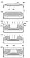
도 1(A)는 반도체 장치의 일 형태를 설명하기 위한 평면도이고, 도 1(B) 내지 도 1(D)는 단면도.
도 2(A) 내지 도 2(E)는 반도체 장치의 제작 방법의 일 형태를 설명하기 위한 단면도.
도 3(A)는 반도체 장치의 일 형태를 설명하기 위한 평면도이고, 도 3(B) 내지 도 3(D)는 단면도.
도 4(A) 내지 도 4(E)는 반도체 장치의 제작 방법의 일 형태를 설명하기 위한 단면도.
도 5(A) 내지 도 5(C)는 반도체 장치의 일 형태를 설명하기 위한 평면도.
도 6(A)는 반도체 장치의 일 형태를 설명하기 위한 평면도이고, 도 6(B)는 단면도.
도 7(A) 및 도 7(B)는 반도체 장치의 일 형태를 도시한 단면도.
도 8(A)는 반도체 장치의 일 형태를 도시한 회로도이고 도 8(B)는 단면도.
도 9(A) 내지 도 9(C)는 전자 기기를 도시한 도면.
도 10(A) 내지 도 10(C)는 전자 기기를 도시한 도면.
도 11은 SIMS 측정 결과를 도시한 도면.
도 12는 희석된 불산을 사용한 처리의 유무와 저항률의 관계를 도시한 그래프.
도 13(A) 및 도 13(B)는 시료 A 및 시료 B의 전기적 특성을 도시한 그래프.
도 14(A) 및 도 14(B)는 시료 C 및 시료 D의 전기적 특성을 도시한 그래프.1 (A) is a plan view for explaining an embodiment of a semiconductor device, and Figs. 1 (B) to 1 (D) are sectional views.
2 (A) to 2 (E) are cross-sectional views for explaining an embodiment of a manufacturing method of a semiconductor device.
3 (A) is a plan view for explaining an embodiment of a semiconductor device, and Fig. 3 (B) to Fig. 3 (D) are sectional views.
4 (A) to 4 (E) are cross-sectional views for explaining an embodiment of a manufacturing method of a semiconductor device.
5 (A) to 5 (C) are plan views for explaining an embodiment of a semiconductor device.
FIG. 6A is a plan view for explaining one embodiment of a semiconductor device, and FIG. 6B is a cross-sectional view.
7 (A) and 7 (B) are cross-sectional views showing one embodiment of a semiconductor device.
8 (A) is a circuit diagram showing one embodiment of a semiconductor device, and Fig. 8 (B) is a sectional view.
9 (A) to 9 (C) are diagrams showing electronic devices.
10 (A) to 10 (C) are diagrams showing electronic devices.
11 is a view showing a result of SIMS measurement.
12 is a graph showing the relationship between the presence or absence of treatment using diluted hydrofluoric acid and the resistivity.
Figs. 13A and 13B are graphs showing electrical characteristics of the sample A and the sample B. Fig.
Figs. 14A and 14B are graphs showing electrical characteristics of the sample C and the sample D. Fig.
본 명세서에 기재된 발명의 실시형태 및 실시예에 대하여 도면을 사용하여 이하에 자세히 설명한다. 다만, 본 명세서에 기재된 발명은 이하의 설명에 한정되지 않고, 그 형태 및 자세한 내용을 다양하게 변경할 수 있다는 것은 당업자라면 용이하게 이해할 수 있다. 또한, 본 명세서에 기재된 발명은 이하의 실시형태 및 실시예의 기재 내용에 한정하여 해석되는 것은 아니다. 또한, 제 1, 제 2 등의 서수사는 편의상 사용하는 것이고, 공정 순서 및 적층 순서를 나타내는 것은 아니다. 또한, 본 명세서에서 발명을 특정하기 위한 사항으로서 고유의 명칭을 나타내는 것은 아니다.BRIEF DESCRIPTION OF THE DRAWINGS Embodiments and embodiments of the invention disclosed herein will be described in detail below with reference to the drawings. It should be understood, however, by those skilled in the art that the invention described herein is not limited to the following description and that various changes in form and detail may be made therein. The invention described in this specification is not to be construed as being limited to the contents of the following embodiments and examples. In addition, the ordinal numbers of the first and second ordinal numbers are used for convenience, and do not indicate the process order and the stacking order. In addition, the specification does not show a unique name as an item for specifying the invention.
(실시형태 1)(Embodiment 1)
본 실시형태에서는 반도체 장치 및 반도체 장치의 제작 방법의 일 형태를 도 1(A) 내지 도 2(E)를 사용하여 설명한다. 본 실시형태에서는 반도체 장치의 일례로서 산화물 반도체막을 갖는 트랜지스터를 나타낸다.In this embodiment mode, one embodiment of a semiconductor device and a manufacturing method of the semiconductor device will be described with reference to FIGS. 1A to 2E. FIG. The present embodiment shows a transistor having an oxide semiconductor film as an example of a semiconductor device.
트랜지스터는 하나의 채널 형성 영역이 형성되는 싱글 게이트 구조이어도 좋고, 2개 형성되는 더블 게이트 구조이어도 좋고, 3개 형성되는 트리플 게이트 구조이어도 좋다. 또한, 게이트 절연막을 개재(介在)하여 채널 형성 영역의 상하에 배치된 2개의 게이트 전극층을 갖는 듀얼 게이트형이라도 좋다.The transistor may be a single gate structure in which one channel formation region is formed, a double gate structure in which two channels are formed, or a triple gate structure in which three channels are formed. Alternatively, a dual gate type in which two gate electrode layers are disposed above and below the channel forming region with a gate insulating film interposed therebetween may be used.
도 1(A) 내지 도 1(C)에 도시된 트랜지스터(410)는 보텀 게이트 구조의 하나이고, 역 스태거형 트랜지스터라고도 하는 트랜지스터의 일례다. 도 1(A)는 트랜지스터(410)의 평면도이고, 도 1(B)는 도 1(A)의 A1-A2를 따라 절단한 단면도(채널 길이 방향의 단면도)이고, 도 1(C)는 도 1(A)의 B1-B2를 따라 절단한 단면도(채널 폭 방향의 단면도)다. 또한, 도 1(A)에서 L은 채널 길이를 나타내고, W는 채널 폭을 나타낸다. 또한, 도 1(A)에서는 복잡화를 피하기 위하여 트랜지스터(410)의 구성 요소의 일부(예를 들어 게이트 절연막(402) 등)를 생략하였다.The
도 1(A) 내지 도 1(C)에 도시된 바와 같이, 트랜지스터(410)를 포함하는 반도체 장치는 절연 표면을 갖는 기판(400) 위에 게이트 전극층(401), 게이트 절연막(402), 산화물 반도체막(403), 소스 전극층(405a) 및 드레인 전극층(405b)을 갖는다. 또한, 트랜지스터(410)를 덮는 절연막(407) 및 평탄화 절연막(408)이 제공되어 있다.1 (A) to 1 (C), a semiconductor device including a
도 1(A) 내지 도 1(C)에 도시된 트랜지스터(410)에서 산화물 반도체막(403)과 절연막(407)의 계면에서의 할로겐 원소(예를 들어 염소 농도)는 5×10¹⁸atoms/cm3 이하, 바람직하게는 1×10¹⁸atoms/cm3 이하로 저감되어 있다. 이로써, 트랜지스터의 백 채널의 저저항화(n형화)가 억제되어 기생 채널의 형성이 억제된 트랜지스터(410)로 할 수 있다. 따라서, 트랜지스터(410)의 고신뢰성화를 도모할 수 있다.The halogen element (for example, the chlorine concentration) at the interface between the
또한, 도 1(A) 및 도 1(C)에 도시된 바와 같이, 트랜지스터(410)에서 소스 전극층(405a) 및 드레인 전극층(405b)은 산화물 반도체막(403)의 채널 폭 W 방향의 단부를 덮는다. 이러한 구성으로 함으로써, 소스 전극층(405a) 및 드레인 전극층(405b)을 형성할 때 산화물 반도체막(403)의 단부가 할로겐 원소를 함유한 에칭 가스를 사용한 플라즈마에 폭로되는 것을 방지할 수 있다.1 (A) and 1 (C), in the
또한, 소스 전극층(405a) 및 드레인 전극층(405b)을 형성할 때 산화물 반도체막(403)의 일부가 제거됨으로써 홈부(오목부)를 갖는 산화물 반도체막(403)이 될 경우가 있다. 또한, 소스 전극층(405a) 및 드레인 전극층(405b)을 형성한 후, 불순물 제거 공정(후술함)을 할 때 산화물 반도체막(403)의 일부가 제거됨으로써 홈부(오목부)를 갖는 산화물 반도체막(403)이 될 경우가 있다. 이 경우에는, 도 1(D)에 도시된 바와 같이, 홈부(오목부)를 갖는 산화물 반도체막(403)을 포함한 트랜지스터(420)가 형성된다. 또한, 트랜지스터(420)의 채널 폭 W 방향의 단면도(도 1(A)의 B1-B2를 따라 절단한 단면도)는 도 1(C)와 마찬가지다.In addition, when the
산화물 반도체막(403)에 사용하는 산화물 반도체로서 인듐(In)을 적어도 함유한다. 특히 인듐(In)과 아연(Zn)을 함유하는 것이 바람직하다. 또한, 상기 산화물 반도체막을 사용한 트랜지스터의 전기 특성의 편차를 감소시키기 위한 스테빌라이저로서 In과 Zn에 추가적으로 갈륨(Ga)을 함유하는 것이 바람직하다. 또한, 스테빌라이저로서 주석(Sn)을 함유하는 것이 바람직하다. 또한, 스테빌라이저로서 하프늄(Hf)을 함유하는 것이 바람직하다. 또한, 스테빌라이저로서 알루미늄(Al)을 함유하는 것이 바람직하다. 또한, 스테빌라이저로서 지르코늄(Zr)을 함유하는 것이 바람직하다.And at least indium (In) is used as an oxide semiconductor used for the
또한, 다른 스테빌라이저로서 란타노이드인 란탄(La), 세륨(Ce), 프라세오디뮴(Pr), 네오디뮴(Nd), 사마륨(Sm), 유로퓸(Eu), 가돌리늄(Gd), 테르븀(Tb), 디스프로슘(Dy), 홀뮴(Ho), 에르븀(Er), 툴륨(Tm), 이테르븀(Yb), 루테튬(Lu) 중 어느 하나 또는 복수 종류를 가져도 좋다.Other stabilizers include lanthanides La, Ce, Pr, Ne, Sm, Eu, Gd, Terbium, Dibromide, (Dy), holmium (Ho), erbium (Er), thulium (Tm), ytterbium (Yb), and lutetium (Lu).
예를 들어 산화물 반도체로서 산화 인듐, 산화 주석, 산화 아연, In-Zn계 산화물, In-Mg계 산화물, In-Ga계 산화물, In-Ga-Zn계 산화물(IGZO라고도 표기함), In-Al-Zn계 산화물, In-Sn-Zn계 산화물, In-Hf-Zn계 산화물, In-La-Zn계 산화물, In-Ce-Zn계 산화물, In-Pr-Zn계 산화물, In-Nd-Zn계 산화물, In-Sm-Zn계 산화물, In-Eu-Zn계 산화물, In-Gd-Zn계 산화물, In-Tb-Zn계 산화물, In-Dy-Zn계 산화물, In-Ho-Zn계 산화물, In-Er-Zn계 산화물, In-Tm-Zn계 산화물, In-Yb-Zn계 산화물, In-Lu-Zn계 산화물, In-Sn-Ga-Zn계 산화물, In-Hf-Ga-Zn계 산화물, In-Al-Ga-Zn계 산화물, In-Sn-Al-Zn계 산화물, In-Sn-Hf-Zn계 산화물, In-Hf-Al-Zn계 산화물을 사용할 수 있다.For example, an oxide semiconductor such as indium oxide, tin oxide, zinc oxide, In - Zn oxide, In - Mg oxide, In - Ga oxide, In - Ga - Zn oxide (also referred to as IGZO) In-Zn-based oxide, In-Hf-Zn-based oxide, In-La-Zn-based oxide, In-Ce-Zn-based oxide, In- Zn-based oxide, In-Zn-Zn-based oxide, In-Sm-Zn-based oxide, In-Zn-Zn-based oxide, In-Gd- In-Zn-Zn oxide, In-Zn-Zn oxide, In-Er-Zn oxide, In-Tm-Zn oxide, In-Yb-Zn oxide, In- In-Sn-Al-Zn-based oxide, In-Sn-Hf-Zn-based oxide and In-Hf-Al-Zn-based oxide can be used.
또한, 여기서는, 예를 들어 In-Ga-Zn계 산화물이란 In, Ga, 및 Zn을 주성분으로서 함유한 산화물을 뜻하고, In, Ga, 및 Zn의 비율은 불문한다. 또한, In, Ga, 및 Zn 외의 금속 원소가 들어 있어도 좋다.Here, for example, the In-Ga-Zn-based oxide means an oxide containing In, Ga, and Zn as main components, and the ratio of In, Ga, and Zn is not limited. In addition, metal elements other than In, Ga, and Zn may be contained.
또한, 산화물 반도체로서 InMO3(ZnO)m(m>0 또 m은 정수가 아님)으로 표기되는 재료를 사용하여도 좋다. 또한, M은 Ga, Fe, Mn, 및 Co 중에서 선택된 하나의 금속 원소 또는 복수의 금속 원소를 나타낸다. 또한, 산화물 반도체로서 In2SnO5(ZnO)n(n>0 또 n은 정수임)으로 표기되는 재료를 사용하여도 좋다.In addition, a material expressed by InMO3 (ZnO)m (m> 0 and m is not an integer) may be used as the oxide semiconductor. Further, M represents one metal element or a plurality of metal elements selected from Ga, Fe, Mn, and Co. Further, a material expressed by In2 SnO5 (ZnO)n (n> 0 and n is an integer) may be used as the oxide semiconductor.
예를 들어 원자수비가 In:Ga:Zn=1:1:1(=1/3:1/3:1/3), In:Ga:Zn=2:2:1(=2/5:2/5:1/5), 또는 In:Ga:Zn=3:1:2(=1/2:1/6:1/3)인 In-Ga-Zn계 산화물이나 그 조성의 근방의 산화물을 사용할 수 있다. 또는, 원자수비가 In:Sn:Zn=1:1:1(=1/3:1/3:1/3), In:Sn:Zn=2:1:3(=1/3:1/6:1/2), 또는 In:Sn:Zn=2:1:5(=1/4:1/8:5/8)인 In-Sn-Zn계 산화물이나 그 조성의 근방의 산화물을 사용하면 좋다.For example, when the atomic ratio is In: Ga: Zn = 1: 1: 1 (= 1/3: 1/3: 1/3), In: Ga: Zn = 2: / 5: 1/5) or In: Ga: Zn = 3: 1: 2 (= 1/2: 1/6: 1/3) Can be used. Or an atomic ratio of In: Sn: Zn = 1: 1: 1 (= 1/3: 1/3: 1/3) Zn-based oxide having an In: Sn: Zn ratio of 2: 1: 5 (= 1/4: 1/8: 5/8) It is good.
그러나, 인듐을 함유한 산화물 반도체는 상술한 것에 한정되지 않고, 필요로 하는 반도체 특성 및 전기 특성(이동도, 임계값, 편차 등)에 따라 적절한 조성을 갖는 것을 사용하면 좋다. 또한, 필요로 하는 반도체 특성을 얻기 위하여 캐리어 농도, 불순물 농도, 결함 밀도, 금속 원소와 산소의 원자수비, 원자간 거리, 밀도 등을 적절한 것으로 하는 것이 바람직하다.However, the oxide semiconductor containing indium is not limited to those described above, and it may be used with an appropriate composition depending on the required semiconductor characteristics and electric characteristics (mobility, threshold value, deviation, etc.). In order to obtain the required semiconductor characteristics, it is preferable that the carrier concentration, the impurity concentration, the defect density, the atomic number ratio of the metal element and the oxygen, the distance between atoms and the density are appropriately set.
예를 들어 In-Sn-Zn계 산화물을 사용한 트랜지스터에서는 비교적 용이하게 높은 이동도를 얻을 수 있다. 그러나, In-Ga-Zn계 산화물을 사용한 트랜지스터에서도 벌크 내 결함 밀도를 낮게 함으로써 이동도를 올릴 수 있다.For example, in a transistor using an In-Sn-Zn oxide, relatively high mobility can be obtained. However, in a transistor using an In-Ga-Zn-based oxide, the mobility can be increased by reducing the defect density in the bulk.
또한, 예를 들어 In, Ga, 및 Zn의 원자수비가 In:Ga:Zn=a:b:c(a+b+c=1)인 산화물의 조성이 원자수비가 In:Ga:Zn=A:B:C(A+B+C=1)인 산화물의 조성의 근방이라는 것은 a, b, c가 (a-A)2+(b-B)2+(c-C)2≤r2를 만족시키는 것을 말하며, r는 예를 들어 0.05로 하면 좋다. 다른 산화물도 마찬가지다.For example, when the composition of an oxide having In, Ga, and Zn atomic ratio ratios of In: Ga: Zn = a: b: c (a + b + c = : b: c is of (a + b + c = 1 ) in the vicinity of the composition of oxide means that satisfying a, b, c a(aA) 2 + (bB) 2 + (cC) 2 ≤r 2, r may be 0.05, for example. The same is true for other oxides.
산화물 반도체막(403)은 단결정, 다결정(폴리크리스탈이라고도 함), 또는 비정질 등의 상태를 갖는다.The
바람직하게는 산화물 반도체막(403)을 CAAC-OS(C Axis Aligned Crystalline Oxide Semiconductor)막으로 한다.Preferably, the
CAAC-OS막은 완전한 단결정이 아니고, 완전한 비정질도 아니다. CAAC-OS막은 비정질상에 결정부를 갖는 결정-비정질 혼상 구조의 산화물 반도체막이다. 또한, 상기 결정부는 하나의 변이 100nm 미만인 입방체 내에 들어가는 크기인 경우가 많다. 또한, 투과형 전자 현미경(TEM: Transmission Electron Microscope)에 의한 관찰상에서는 CAAC-OS막에 포함되는 비정질부와 결정부의 경계는 명확하지 않다. 또한, TEM에 의한 관찰상에서는 CAAC-OS막에 입계(그레인 바운더리(grain boundary)라고도 함)는 확인되지 않는다. 그러므로, CAAC-OS막은 입계에 기인한 전자 이동도의 저하가 억제된다.The CAAC-OS film is neither a complete single crystal nor a complete amorphous. The CAAC-OS film is an oxide semiconductor film having a crystal-amorphous mixed phase structure having an amorphous phase and a crystal part. In addition, the crystal portion is often of such a size that one side falls within a cube of less than 100 nm. In addition, the boundary between the amorphous portion and the crystalline portion included in the CAAC-OS film is not clear on observation by a transmission electron microscope (TEM). In addition, on the observation by TEM, grain boundaries (also referred to as grain boundaries) are not confirmed in the CAAC-OS film. Therefore, the CAAC-OS film is suppressed from lowering the electron mobility due to the grain boundary.
CAAC-OS막에 포함되는 결정부는 c축이 CAAC-OS막의 피형성면의 법선 벡터 또는 표면의 법선 벡터에 평행한 방향으로 정렬되고, 또 ab면에 수직인 방향으로부터 볼 때 삼각형 또는 육각형의 원자 배열을 갖고, c축에 수직인 방향으로부터 볼 때 금속 원자가 층상 또는 금속 원자와 산소 원자가 층상으로 배열되어 있다. 또한, 상이한 결정부의 a축 및 b축의 방향이 서로 달라도 좋다. 본 명세서에서 단순히 '수직'이라고 기재한 경우에는, 85° 이상 95° 이하의 범위도 포함되는 것으로 한다. 또한, 단순히 '평행'이라고 기재한 경우에는, -5° 이상 5° 이하의 범위도 포함되는 것으로 한다.The crystal part included in the CAAC-OS film is arranged such that the c-axis is aligned in a direction parallel to the normal vector of the surface to be formed of the CAAC-OS film or the normal vector of the surface, and the triangular or hexagonal atom And the metal atoms are arranged in layers or in the form of layers of metal atoms and oxygen atoms when viewed from the direction perpendicular to the c axis. The directions of the a-axis and the b-axis of the different crystal portions may be different from each other. In the present specification, when it is simply referred to as " vertical ", it is assumed that the range of 85 DEG to 95 DEG is also included. In the case of simply describing "parallel", the range of -5 ° to 5 ° is also included.
또한, CAAC-OS막에서 결정부의 분포가 균일하지 않아도 좋다. 예를 들어 CAAC-OS막의 형성 과정에서 산화물 반도체막의 표면 측으로부터 결정 성장시키는 경우에는, 피형성면 근방보다 표면 근방에서 결정부가 차지하는 비율이 높은 경우가 있다. 또한, CAAC-OS막에 불순물을 첨가함으로써 상기 불순물 첨가 영역에서 결정부가 비정질화되는 경우도 있다.Also, the distribution of the crystal portions in the CAAC-OS film need not be uniform. For example, when the crystal is grown from the surface side of the oxide semiconductor film in the process of forming the CAAC-OS film, the ratio of the crystal portion in the vicinity of the surface may be higher than in the vicinity of the surface to be formed. In addition, by adding an impurity to the CAAC-OS film, the crystalline portion may be amorphized in the impurity added region.
CAAC-OS막에 포함되는 결정부의 c축은 CAAC-OS막의 피형성면의 법선 벡터 또는 표면의 법선 벡터에 평행한 방향으로 정렬되기 때문에, CAAC-OS막의 형상(피형성면의 단면 형상 또는 표면의 단면 형상)에 따라서는 서로 다른 방향을 향하는 경우가 있다. 또한, 결정부의 c축 방향은 CAAC-OS막이 형성되었을 때의 피형성면의 법선 벡터 또는 표면의 법선 벡터에 평행한 방향이 된다. 막 형성에 의하여 또는 막 형성 후의 가열 처리 등의 결정화 처리에 의하여 결정부가 형성된다.Since the c-axis of the crystal part included in the CAAC-OS film is aligned in a direction parallel to the normal vector of the surface to be imaged or the normal vector of the surface of the CAAC-OS film, the shape of the CAAC- Sectional shape) may be directed in different directions. The c-axis direction of the crystal portion is parallel to the normal vector of the surface to be formed or the normal vector of the surface when the CAAC-OS film is formed. Crystallization portions are formed by film formation or crystallization processing such as heat treatment after film formation.
CAAC-OS막을 사용한 트랜지스터는 가시광이나 자외광의 조사로 인한 전기 특성의 변동을 저감시킬 수 있다. 따라서, 상기 트랜지스터는 신뢰성이 높다.Transistors using a CAAC-OS film can reduce variations in electrical characteristics due to irradiation of visible light and ultraviolet light. Therefore, the transistor is highly reliable.
또한, 산화물 반도체막을 구성하는 산소의 일부는 질소로 치환되어도 좋다.Further, a part of oxygen constituting the oxide semiconductor film may be substituted with nitrogen.
또한, CAAC-OS와 같이 결정부를 갖는 산화물 반도체에서는 벌크 내 결함을 더 저감시킬 수 있고, 표면의 평탄성을 높이면 비정질 상태의 산화물 반도체 이상의 이동도를 얻을 수 있다. 표면의 평탄성을 높이기 위해서는 평탄한 표면 위에 산화물 반도체를 형성하는 것이 바람직하고, 구체적으로는 평균 면 거칠기(Ra)가 1nm 이하, 바람직하게는 0.3nm 이하, 더 바람직하게는 0.1nm 이하의 표면 위에 형성하면 좋다.Further, in an oxide semiconductor having a crystal part such as CAAC-OS, defects in a bulk can be further reduced, and mobility higher than that of an amorphous oxide semiconductor can be obtained by increasing the surface flatness. In order to increase the flatness of the surface, it is preferable to form an oxide semiconductor on a flat surface. Specifically, the oxide semiconductor is formed on a surface having an average surface roughness (Ra) of 1 nm or less, preferably 0.3 nm or less, more preferably 0.1 nm or less good.
또한, Ra란 JIS B 0601:2001(ISO4287:1997)로 정의되는 산술 평균 거칠기를 곡면에 적용할 수 있도록 3차원으로 확장한 것이며, 기준면으로부터 지정면까지의 편차의 절대값을 평균한 값으로 표현할 수 있고, 수학식 1로 정의된다.In addition, Ra is a three-dimensional extension of the arithmetic average roughness defined by JIS B 0601: 2001 (ISO4287: 1997) so that it can be applied to a curved surface. It can be expressed as an average of absolute values of deviations from a reference surface to a designated surface And is defined by Equation (1).

여기서 지정면이란 거칠기 계측 대상이 되는 면이고, 좌표(x1, y1, f(x1, y1)), (x1, y2, f(x1, y2)), (x2, y1, f(x2, y1)), (x2, y2, f(x2, y2))의 4지점을 연결하여 이루어진 사각형의 영역으로 하고, 지정면을 xy 평면에 투영한 장방형의 면적을 S0, 기준면의 높이(지정면의 평균의 높이)를 Z0으로 한다. Ra는 원자간력 현미경(AFM: Atomic Force Microscope)으로 측정할 수 있다.Wherein designating area is a surface where the roughness measurement target, the coordinates(x 1, y 1, f (x 1, y 1)), (x 1, y 2, f (x 1, y 2)), (x 2,y 1, f (x 2, y 1)), (x 2, y 2, f (x 2, y 2)) of the rectangular connecting the fourth point to and the area of the formed square, projecting a designating area in the xy plane to the area of S0, the height of the reference surface (the average height of the designating area) as the Z0. Ra can be measured with an atomic force microscope (AFM).
다만, 본 실시형태에서 설명하는 트랜지스터(410)는 보텀 게이트형이기 때문에 산화물 반도체막 아래 쪽에 기판(400), 게이트 전극층(401), 및 게이트 절연막(402)이 존재한다. 따라서, 상기 평탄한 표면을 얻기 위해서는 게이트 전극층(401) 및 게이트 절연막(402)을 형성한 후, CMP 처리 등의 평탄화 처리를 하여도 좋다.However, since the
산화물 반도체막(403)의 막 두께는 1nm 이상 30nm 이하(바람직하게는, 5nm 이상 10nm 이하)로 하고, 스퍼터링법, MBE(Molecular Beam Epitaxy)법, CVD법, 펄스레이저 퇴적법, ALD(Atomic Layer Deposition)법 등을 적절히 사용할 수 있다. 또한, 산화물 반도체막(403)은 스퍼터링 타깃 표면에 대략 수직으로 복수의 기판 표면이 세트된 상태에서 성막하는 스퍼터링 장치를 사용하여 성막하여도 좋다.The
다음에, 도 2(A) 내지 도 2(E)에 트랜지스터(410)를 갖는 반도체 장치의 제작 방법의 일례를 도시하였다.Next, an example of a manufacturing method of a semiconductor device having the
절연 표면을 갖는 기판(400)에 사용할 수 있는 기판에 큰 제한은 없지만, 적어도 이후의 가열 처리에 견딜 수 있을 정도의 내열성을 가질 필요가 있다. 예를 들어 바륨 보로실리케이트 유리나 알루미노 보로실리케이트 유리 등의 유리 기판, 세라믹 기판, 석영 기판, 사파이어 기판 등을 사용할 수 있다. 또한, 실리콘이나 탄소화 실리콘 등으로 이루어진 단결정 반도체 기판이나 다결정 반도체 기판, 실리콘게르마늄 등으로 이루어진 화합물 반도체 기판, SOI 기판 등을 적용할 수도 있고, 이들 기판 위에 반도체 소자가 제공된 것을 기판(400)으로서 사용하여도 좋다.There is no particular limitation on the substrate that can be used for the
또한, 기판(400)으로서 가요성 기판을 사용하여 반도체 장치를 제작하여도 좋다. 가요성을 갖는 반도체 장치를 제작하기 위해서는 가요성 기판 위에 산화물 반도체막(403)을 포함하는 트랜지스터(410)를 직접 제작하여도 좋고, 다른 제작 기판에 산화물 반도체막(403)을 포함하는 트랜지스터(410)를 제작하고, 그 후에 박리하고 가요성 기판으로 전치하여도 좋다. 또한, 제작 기판으로부터 박리하고 가요성 기판으로 전치하기 위하여 제작 기판과 산화물 반도체막을 포함하는 트랜지스터(410) 사이에 박리층을 제공하면 좋다.Further, a semiconductor device may be manufactured using the flexible substrate as the
기판(400) 위에 하지막으로서 절연막을 형성하여도 좋다. 절연막으로서는 플라즈마 CVD법 또는 스퍼터링법 등에 의하여 산화 실리콘, 산화 질화 실리콘, 산화 알루미늄, 산화 질화 알루미늄, 산화 하프늄, 및 산화 갈륨 등의 산화물 절연 재료, 질화 실리콘, 질화 산화 실리콘, 질화 알루미늄, 및 질화 산화 알루미늄 등의 질화물 절연 재료, 또는 이들의 혼합 재료를 사용하여 형성할 수 있다.An insulating film may be formed on the
기판(400)(또는 기판(400) 및 절연막)에 가열 처리하여도 좋다. 예를 들어 고온 가스를 사용하여 가열 처리하는 GRTA(Gas Rapid Thermal Anneal) 장치에 의하여 650℃로 1분 내지 5분간 동안 가열 처리하면 좋다. 또한, GRTA에서의 고온 가스에는 아르곤 등의 희가스, 또는 질소와 같은 가열 처리에 의하여 피처리물과 반응하지 않는 불활성 기체가 사용된다. 또한, 전기로에 의하여 500℃로 30분 내지 1시간 동안 가열 처리하여도 좋다.The substrate 400 (or the
다음에, 기판(400) 위에 게이트 전극층(이것과 같은 층으로 형성되는 배선을 포함함)이 되는 도전막을 형성한다. 도전막은 몰리브덴, 티타늄, 탄탈, 텅스텐, 알루미늄, 구리, 크롬, 네오디뮴, 스칸듐 등의 금속 재료 또는 이들을 주성분으로 하는 합금 재료를 사용하여 형성할 수 있다. 또한, 도전막으로서 인 등의 불순물 원소를 도핑한 다결정 실리콘막으로 대표되는 반도체막, 니켈 실리사이드 등의 실리사이드막을 사용하여도 좋다. 도전막은 단층 구조와 적층 구조의 어느 쪽을 가져도 좋다.Next, on the
또한, 도전막의 재료로서 산화 인듐-산화 주석, 산화 텅스텐을 함유한 인듐 산화물, 산화 텅스텐을 함유한 인듐 아연 산화물, 산화 티타늄을 함유한 인듐 산화물, 산화 티타늄을 함유한 인듐 주석 산화물, 산화 인듐-산화 아연, 산화 실리콘을 첨가한 인듐 주석 산화물 등의 도전성 재료를 적용할 수도 있다. 또한, 상기 도전성 재료와 상기 금속 재료의 적층 구조로 할 수도 있다.The material of the conductive film may also be indium oxide-tin oxide, indium oxide containing tungsten oxide, indium zinc oxide containing tungsten oxide, indium oxide containing titanium oxide, indium tin oxide containing titanium oxide, indium oxide Zinc, and indium tin oxide doped with silicon oxide may be used. Further, a laminated structure of the conductive material and the metal material may be used.
또한, 게이트 절연막(402)과 접촉되는 도전막으로서 질소를 함유한 금속 산화물, 구체적으로는 질소를 함유한 In-Ga-Zn-O막, 질소를 함유한 In-Sn-O막, 질소를 함유한 In-Ga-O막, 질소를 함유한 In-Zn-O막, 질소를 함유한 Sn-O막, 질소를 함유한 In-O막, 금속 질화막(InN, SnN 등)을 사용할 수 있다. 이들 막은 5eV, 바람직하게는 5.5eV 이상의 일 함수를 가지며 게이트 전극층으로서 사용한 경우에는, 트랜지스터의 전기 특성의 임계값 전압을 플러스로 할 수 있기 때문에 소위 노멀리 오프의 스위칭 소자를 실현할 수 있다.In addition, as the conductive film in contact with the
본 실시형태에서는 스퍼터링법에 의하여 막 두께가 100nm인 텅스텐막을 형성한다.In this embodiment mode, a tungsten film having a thickness of 100 nm is formed by a sputtering method.
다음에, 포토리소그래피 공정에 의하여 도전막 위에 레지스트 마스크를 형성하고, 선택적으로 에칭하여 게이트 전극층(401)을 형성한다. 게이트 전극층(401)을 형성한 후, 레지스트 마스크를 제거한다. 도전막의 에칭은 드라이 에칭이라도 좋고, 웨트 에칭이라도 좋고, 양쪽 모두를 사용하여도 좋다.Next, a resist mask is formed on the conductive film by a photolithography process, and the
또한, 게이트 전극층(401)을 형성한 후에 기판(400) 및 게이트 전극층(401)에 가열 처리하여도 좋다. 예를 들어 GRTA 장치에 의하여 650℃로 1분 내지 5분 동안 가열 처리하면 좋다. 또한, 전기로에 의하여 500℃로 30분 내지 1시간 동안 가열 처리하여도 좋다.The
다음에, 게이트 전극층(401) 위에 게이트 절연막(402)을 형성한다.Next, a
또한, 게이트 절연막(402)의 피복성을 향상시키기 위하여 게이트 전극층(401) 표면에 평탄화 처리하여도 좋다. 특히, 게이트 절연막(402)으로서 막 두께가 얇은 절연막을 사용하는 경우에는, 게이트 전극층(401) 표면의 평탄성이 양호한 것이 바람직하다.The surface of the
게이트 절연막(402)의 막 두께는 1nm 이상 20nm 이하로 하고, 스퍼터링법, MBE법, CVD법, PECVD법, 펄스 레이저 퇴적법, ALD법 등을 적절히 사용할 수 있다. 또한, 게이트 절연막(402)은 스퍼터링 타깃 표면에 대략 수직으로 복수의 기판 표면이 세트된 상태에서 성막하는 스퍼터링 장치를 사용하여 형성하여도 좋다.The film thickness of the
게이트 절연막(402)은 산화 실리콘막, 산화 갈륨막, 산화 알루미늄막, 질화 실리콘막, 산화 질화 실리콘막, 산화 질화 알루미늄막, 또는 질화 산화 실리콘막을 재료로서 사용하여 형성할 수 있다. 또한, 게이트 절연막(402)의 재료로서 산화 하프늄, 산화 이트륨, 하프늄 실리케이트(HfSixOy(x>0, y>0)), 질소가 첨가된 하프늄 실리케이트(HfSiOxNy(x>0, y>0)), 하프늄 알루미네이트(HfAlxOy(x>0, y>0)), 산화 란탄 등의 high-k 재료를 사용함으로써 게이트 누설 전류를 저감시킬 수 있다. 또한, 게이트 절연막(402)은 상기 재료를 사용하여 단층 구조 또는 적층 구조로 형성된다.The
게이트 절연막(402)은 산화물 반도체막(403)과 접촉된 부분에 산소를 함유하는 것이 바람직하다. 특히, 게이트 절연막(402)은 막 내(벌크 내)에 적어도 화학양론비를 초과하는 양의 산소가 존재하는 것이 바람직하고, 예를 들어 게이트 절연막(402)으로서 산화 실리콘막을 사용하는 경우에는, SiO2+α(다만, α>0)로 한다.It is preferable that the
산소의 공급원이 되는 산소를 많이(과잉으로) 함유한 게이트 절연막(402)을 산화물 반도체막(403)과 접촉되도록 형성함으로써, 상기 게이트 절연막(402)으로부터 산화물 반도체막(403)으로 산소를 공급할 수 있다. 산화물 반도체막(403)과 게이트 절연막(402)이 적어도 부분적으로 접촉된 상태에서 가열 처리함으로써 산화물 반도체막(403)에 산소를 공급하여도 좋다.Oxygen can be supplied from the
산화물 반도체막(403)에 산소를 공급함으로써, 막 내의 산소 결손을 보전할 수 있다. 또한, 제작하는 트랜지스터의 크기나 게이트 절연막(402)의 단차 피복성을 고려하여 게이트 절연막(402)을 형성하는 것이 바람직하다.By supplying oxygen to the
본 실시형태에서는 고밀도 플라즈마 CVD법에 의하여 막 두께가 200nm인 산화 질화 실리콘막을 형성한다.In this embodiment, a silicon oxynitride film having a film thickness of 200 nm is formed by a high density plasma CVD method.
또한, 게이트 절연막(402)을 형성한 후에 기판(400), 게이트 전극층(401), 및 게이트 절연막(402)에 가열 처리하여도 좋다. 예를 들어 GRTA 장치에 의하여 650℃로 1분 내지 5분 동안 가열 처리하면 좋다. 또한, 전기로에 의하여 500℃로 30분 내지 1시간 동안 가열 처리하여도 좋다.The
다음에, 게이트 절연막(402) 위에 산화물 반도체막(403)을 형성한다(도 2(A) 참조).Next, an
산화물 반도체막(403)의 형성 공정에서 산화물 반도체막(403)에 수소 또는 물이 가능한 한 함유되지 않도록 하기 위하여, 산화물 반도체막(403)의 형성의 전처리로서 스퍼터링 장치의 예비 가열실에서 게이트 절연막(402)이 형성된 기판을 예비 가열함으로써, 기판 및 게이트 절연막(402)에 흡착된 수소나 수분 등의 불순물을 탈리시켜 배기하는 것이 바람직하다. 또한, 예비 가열실에 설치하는 배기 수단은 크라이오 펌프(cryo pump)가 바람직하다.In order to prevent hydrogen or water from being contained in the
게이트 절연막(402)에서 산화물 반도체막(403)이 접촉하여 형성될 영역을 평탄화 처리하여도 좋다. 평탄화 처리로서는 특별히 한정되지 않지만, 연마 처리(예를 들어 화학적 기계 연마(Chemical Mechanical Polishing: CMP)법), 드라이 에칭 처리, 플라즈마 처리를 사용할 수 있다.A region in which the
플라즈마 처리로서 예를 들어 아르곤 가스를 도입하여 플라즈마를 발생시키는 역 스퍼터링을 할 수 있다. 역 스퍼터링이란 아르곤 분위기하에서 기판 측에 RF 전원을 사용하여 전압을 인가하여 기판 근방에 플라즈마를 형성하여 표면을 개질하는 방법이다. 또한, 아르곤 분위기 대신에 질소, 헬륨, 산소 등을 사용하여도 좋다. 역 스퍼터링에 의하여 게이트 절연막(402) 표면에 부착되어 있는 가루 상태의 물질(파티클, 먼지라고도 함)이 제거될 수 있다.As the plasma treatment, for example, argon gas may be introduced to perform reverse sputtering in which plasma is generated. Inverse sputtering is a method in which a voltage is applied to the substrate side in an argon atmosphere using an RF power source to form a plasma in the vicinity of the substrate to modify the surface. Further, nitrogen, helium, oxygen or the like may be used instead of the argon atmosphere. The powdery substance (also referred to as particles or dust) attached to the surface of the
평탄화 처리로서 연마 처리, 드라이 에칭 처리, 및 플라즈마 처리는 여러 번 하여도 좋고, 이들을 조합하여 행하여도 좋다. 또한, 조합하여 행하는 경우에는, 공정 순서도 특별히 한정되지 않고, 게이트 절연막(402) 표면의 요철 상태에 따라 적절히 설정하면 좋다.As the planarization treatment, the polishing treatment, the dry etching treatment, and the plasma treatment may be repeated several times or may be performed in combination. In the case of combining them, the process sequence is not particularly limited, and may be suitably set in accordance with the surface irregularities of the surface of the
또한, 성막할 때에 산소가 많이 함유되는 조건(예를 들어 산소 비율이 100%인 분위기하에서 스퍼터링법에 의하여 막을 형성함)하에서 산화물 반도체막(403)을 형성함으로써 산소를 많이 함유한(바람직하게는 산화물 반도체가 결정 상태에서의 화학량론적 조성을 초과하는 양의 산소를 함유한 영역을 포함하는) 막으로 하는 것이 바람직하다.Further, by forming the
또한, 본 실시형태에서 산화물 반도체막(403)으로서 AC 전원 장치를 갖는 스퍼터링 장치를 사용한 스퍼터링법을 사용하여 막 두께가 35nm인 In-Ga-Zn계 산화물막(IGZO막)을 형성한다. 본 실시형태에서 원자수비가 In:Ga:Zn=1:1:1(=1/3:1/3:1/3)인 In-Ga-Zn계 산화물 타깃을 사용한다. 또한, 성막 조건은 산소 및 아르곤 분위기하(산소 유량 비율이 50%), 압력 0.6Pa, 전원 전력 5kW, 기판 온도 170℃로 한다. 이 성막 조건하에서의 성막 속도는 16nm/min이다.In this embodiment, an In-Ga-Zn-based oxide film (IGZO film) having a film thickness of 35 nm is formed by sputtering method using a sputtering apparatus having an AC power source device as the
산화물 반도체막(403)을 형성할 때에 사용하는 스퍼터링 가스는 수소, 물, 수산기, 또는 수소화물 등의 불순물이 제거된 고순도 가스를 사용하는 것이 바람직하다.The sputtering gas used when forming the
감압 상태로 유지된 성막실 내에 기판을 유지한다. 그리고, 성막실 내의 잔류 수분을 제거하면서, 수소 및 수분이 제거된 스퍼터링 가스를 도입하고, 상기 타깃을 사용하여 기판(400) 위에 산화물 반도체막(403)을 형성한다. 성막실 내의 잔류 수분을 제거하기 위해서는 흡착형 진공 펌프 예를 들어 크라이오 펌프, 이온 펌프, 티타늄 서블리메이션 펌프를 사용하는 것이 바람직하다. 또한, 배기 수단으로서는 터보 분자 펌프에 콜드 트랩(cold trap)이 장착된 것이어도 좋다. 크라이오 펌프를 사용하여 배기된 성막실은 예를 들어 수소 원자나 물(H2O) 등 수소 원자를 함유한 화합물(더 바람직하게는 탄소 원자를 함유한 화합물도) 등이 배기되므로, 상기 성막실에서 형성된 산화물 반도체막(403)에 함유되는 수소, 물, 수산기, 또는 수소화물 등의 불순물 농도를 저감시킬 수 있다.The substrate is held in the deposition chamber kept in a reduced pressure state. Then, while removing residual moisture in the deposition chamber, hydrogen and moisture-free sputtering gas is introduced, and the
또한, 게이트 절연막(402)을 대기에 개방시키지 않고 게이트 절연막(402)과 산화물 반도체막(403)을 연속적으로 형성하는 것이 바람직하다. 게이트 절연막(402)을 대기에 폭로시키지 않고 게이트 절연막(402)과 산화물 반도체막(403)을 연속적으로 형성하면, 게이트 절연막(402) 표면에 수소나 수분 등의 불순물이 흡착되는 것을 방지할 수 있다.It is also preferable that the
막 형상 산화물 반도체막을 포토리소그래피 공정에 의하여 섬 형상 산화물 반도체막으로 가공함으로써 산화물 반도체막(403)을 형성할 수 있다.The
또한, 섬 형상 산화물 반도체막(403)을 형성하기 위한 레지스트 마스크를 잉크젯법으로 형성하여도 좋다. 레지스트 마스크를 잉크젯법으로 형성하면 포토마스크를 사용하지 않기 때문에 제조 비용을 저감시킬 수 있다.Further, a resist mask for forming the island-shaped
또한, 산화물 반도체막의 에칭으로서 드라이 에칭 및 웨트 에칭 중 어느 쪽을 사용하여도 좋고, 양쪽 모두를 사용하여도 좋다. 예를 들어 산화물 반도체막의 웨트 에칭에 사용하는 에칭액으로서는 인산, 초산, 및 질산을 혼합한 용액 등을 사용할 수 있다. 또한, ITO-07N(KANTO CHEMICAL CO.,INC 제작)을 사용하여도 좋다. 또한, ICP(Inductively Coupled Plasma: 유도 결합형 플라즈마) 에칭법을 사용한 드라이 에칭에 의하여 에칭 가공하여도 좋다.Either dry etching or wet etching may be used as the etching of the oxide semiconductor film, or both of them may be used. For example, a solution obtained by mixing phosphoric acid, acetic acid, and nitric acid or the like can be used as the etching solution used for wet etching of the oxide semiconductor film. ITO-07N (manufactured by KANTO CHEMICAL CO. INC.) May also be used. Alternatively, etching may be performed by dry etching using an ICP (Inductively Coupled Plasma) etching method.
또한, 산화물 반도체막(403)에 과잉의 수소(물이나 수산기를 포함함)를 제거(탈수화 또는 탈수소화)하기 위한 가열 처리를 하여도 좋다. 가열 처리의 온도는 300℃ 이상 700℃ 이하 또는 기판의 변형점 미만으로 한다. 감압하 또는 질소 분위기하 등에서 가열 처리를 할 수 있다.Further, the
또한, 산화물 반도체막(403)으로서 결정성 산화물 반도체막을 사용하는 경우에는, 결정화를 위한 가열 처리를 하여도 좋다.When a crystalline oxide semiconductor film is used as the
본 실시형태에서는 가열 처리 장치의 하나인 전기로에 기판을 도입하고, 산화물 반도체막(403)에 질소 분위기하에서 450℃로 1시간 동안의 가열 처리 및 질소 및 산소 분위기하에서 450℃로 1시간 동안의 가열 처리를 한다.In this embodiment mode, a substrate is introduced into an electric furnace, which is one of the heat treatment apparatuses, and the
또한, 가열 처리 장치는 전기로에 한정되지 않고, 저항 발열체 등의 발열체로부터의 열전도 또는 열복사에 의하여 피처리물을 가열하는 장치를 사용하여도 좋다. 예를 들어 GRTA(Gas Rapid Thermal Anneal) 장치, LRTA(Lamp Rapid Thermal Anneal) 장치 등의 RTA(Rapid Thermal Anneal) 장치를 사용할 수 있다. LRTA 장치는 할로겐 램프, 메탈할라이드 램프, 크세논 아크 램프, 카본 아크 램프, 고압 나트륨 램프, 고압 수은 램프 등의 램프로부터 발하는 빛(전자기파)의 복사에 의하여 피처리물을 가열하는 장치다. GRTA 장치는 고온 가스를 사용하여 가열 처리하는 장치다. 고온 가스로서 아르곤 등의 희가스, 또는 질소와 같은 가열 처리에 의하여 피처리물과 반응하지 않는 불활성 기체가 사용된다.Further, the heat treatment apparatus is not limited to an electric furnace, and an apparatus for heating the article to be treated by heat conduction from a heating element such as a resistance heating element or by thermal radiation may be used. For example, an RTA (Rapid Thermal Anneal) device such as a GRTA (Gas Rapid Thermal Anneal) device or an LRTA (Lamp Rapid Thermal Anneal) device can be used. The LRTA device is a device for heating a material to be irradiated by radiating light (electromagnetic waves) emitted from a lamp such as a halogen lamp, a metal halide lamp, a xenon arc lamp, a carbon arc lamp, a high pressure sodium lamp or a high pressure mercury lamp. The GRTA apparatus is a device for performing heat treatment using a high temperature gas. As the high-temperature gas, a rare gas such as argon or an inert gas which does not react with the object to be treated by a heat treatment such as nitrogen is used.
예를 들어 가열 처리로서 650℃ 내지 700℃의 고온으로 가열한 불활성 가스 중에 기판을 넣고 수분간 가열한 후 기판을 불활성 가스 중에서 꺼내는 GRTA 처리를 하여도 좋다.For example, as a heat treatment, a substrate may be placed in an inert gas heated to a high temperature of 650 ° C to 700 ° C, the substrate may be heated for several minutes, and the substrate may be subjected to a GRTA treatment to remove the substrate from the inert gas.
또한, 가열 처리에서 질소, 또는 헬륨, 네온, 아르곤 등의 희가스에 물, 수소 등이 함유되지 않는 것이 바람직하다. 또는, 가열 처리 장치에 도입하는 질소, 또는 헬륨, 네온, 아르곤 등의 희가스의 순도를 6N(99.9999%) 이상, 바람직하게는 7N(99.99999%) 이상(즉 불순물 농도를 1ppm 이하, 바람직하게는 0.1ppm 이하)으로 하는 것이 바람직하다.It is also preferable that the rare gas such as nitrogen, helium, neon or argon does not contain water, hydrogen or the like in the heat treatment. Nitrogen, or rare gas such as helium, neon, argon, or the like introduced into the heat treatment apparatus to a purity of 6N (99.9999%) or more, preferably 7N (99.99999%) or more (i.e., an impurity concentration of 1 ppm or less, ppm or less).
또한, 가열 처리로 산화물 반도체막(403)을 가열한 후, 동일한 노에 고순도의 산소 가스, 고순도의 일산화 이질소 가스, 또는 초건조 에어(CRDS(캐비티 링다운 레이저 분광법) 방식의 노점계를 사용하여 측정한 경우의 수분량이 20ppm(노점 환산으로 -55℃) 이하, 바람직하게는 1ppm 이하, 더 바람직하게는 10ppb 이하의 공기)를 도입하여도 좋다. 산소 가스 또는 일산화 이질소 가스에 물, 수소 등이 함유되지 않는 것이 바람직하다. 또는, 가열 처리 장치에 도입하는 산소 가스 또는 일산화 이질소 가스의 순도를 6N 이상 바람직하게는 7N 이상(즉 산소 가스 또는 일산화 이질소 가스 중의 불순물 농도를 1ppm 이하, 바람직하게는 0.1ppm 이하)으로 하는 것이 바람직하다. 탈수화 또는 탈수소화 처리에 의한 불순물의 배제 공정을 거쳐 감소된 산화물 반도체를 구성하는 주성분 재료인 산소를 산소 가스 또는 일산화 이질소 가스의 작용에 의하여 공급함으로써, 산화물 반도체막(403)을 고순도화 및 i형(진성)화할 수 있다.Further, after the
또한, 탈수화 또는 탈수소화를 위한 가열 처리의 타이밍은 막 형상 산화물 반도체막의 형성 후와 섬 형상 산화물 반도체막(403)을 형성한 후의 어느 쪽이라도 좋다.The timing of the heat treatment for dehydration or dehydrogenation may be either after formation of the film-shaped oxide semiconductor film or after formation of the island-shaped
또한, 탈수화 또는 탈수소화를 위한 가열 처리는 여러 번 하여도 좋고 다른 가열 처리를 겸하여도 좋다.Further, the heat treatment for dehydration or dehydrogenation may be performed several times or may be combined with other heat treatment.
산화물 반도체막(403)으로서 섬 형상으로 가공되기 전에 막 형상 산화물 반도체막이 게이트 절연막(402)을 덮은 상태에서 탈수화 또는 탈수소화를 위한 가열 처리를 하면, 게이트 절연막(402)에 함유된 산소가 가열 처리에 의하여 방출되는 것을 방지할 수 있기 때문에 바람직하다.When the film-like oxide semiconductor film is covered with the
또한, 탈수화 또는 탈수소화 처리된 산화물 반도체막(403)에 산소(적어도 산소 라디칼, 산소 원자, 산소 이온 중 어느 것을 포함함)를 도입하여 막 내에 산소를 공급하여도 좋다.Further, oxygen may be supplied into the film by introducing oxygen (including at least oxygen radicals, oxygen atoms, and oxygen ions) into the
또한, 탈수화 또는 탈수소화 처리에 의하여 산화물 반도체를 구성하는 주성분 재료인 산소도 탈리하여 감소될 우려가 있다. 산화물 반도체막의 산소가 탈리된 개소에서는 산소 결손이 존재하고, 상기 산소 결손에 기인하여 트랜지스터의 전기적 특성 변동을 초래하는 도너 준위가 생긴다.In addition, oxygen, which is a main component material constituting the oxide semiconductor, may also be desorbed by the dehydration or dehydrogenation treatment. Oxygen vacancies exist in a portion where oxygen is eliminated from the oxide semiconductor film, and a donor level is generated which causes variations in electrical characteristics of the transistor due to the oxygen vacancies.
따라서, 탈수화 또는 탈수소화 처리된 산화물 반도체막에 산소(적어도 산소 라디칼, 산소 원자, 산소 이온 중 어느 것을 포함함)를 공급하는 것이 바람직하다. 산화물 반도체막에 산소를 공급함으로써, 막 내의 산소 결손을 보전할 수 있다.Therefore, it is preferable to supply oxygen (including at least oxygen radicals, oxygen atoms, and oxygen ions) to the dehydrated or dehydrogenated oxide semiconductor film. By supplying oxygen to the oxide semiconductor film, oxygen deficiency in the film can be preserved.
탈수화 또는 탈수소화 처리된 산화물 반도체막(403)에 산소를 도입하여 막 내에 산소를 공급함으로써 산화물 반도체막(403)을 고순도화 및 i형(진성)화할 수 있다. 고순도화되고 i형(진성)화된 산화물 반도체막(403)을 갖는 트랜지스터는 전기적 특성 변동이 억제되고 전기적으로 안정적이다.Oxygen is introduced into the dehydrated or dehydrogenated
산소를 도입하는 방법으로서는 이온 주입법, 이온 도핑법, 플라즈마 이머전 이온 임플랜테이션법, 플라즈마 처리 등을 사용할 수 있다.As the method of introducing oxygen, ion implantation method, ion doping method, plasma immersion ion implantation method, plasma treatment and the like can be used.
산화물 반도체막(403)에 산소를 도입하는 경우에는, 산화물 반도체막(403)에 직접 산소를 도입하여도 좋고, 이후 형성될 절연막(407) 등 다른 막을 통과시켜 산화물 반도체막(403)에 산소를 도입하여도 좋다. 다른 막을 통과시켜 산소를 도입하는 경우에는, 이온 주입법, 이온 도핑법, 플라즈마 이머전 이온 임플랜테이션법 등을 사용하면 좋지만, 노출된 산화물 반도체막(403)에 산소를 직접 도입하는 경우에는 플라즈마 처리 등도 사용할 수 있다.When oxygen is introduced into the
산화물 반도체막(403)으로의 산소 도입의 타이밍은 탈수화 또는 탈수소화 처리된 후이면 바람직하지만, 특별히 한정되지 않는다. 또한, 상기 탈수화 또는 탈수소화 처리된 산화물 반도체막(403)으로의 산소 도입은 여러 번 하여도 좋다.The timing of introduction of oxygen into the
트랜지스터에 형성되는 산화물 반도체막을 결정 상태의 산화물 반도체의 화학량론적 조성을 초과하는 양의 산소를 함유한 영역이 포함되는 막으로 하면 바람직하다. 이 경우에 산소의 함유량은 산화물 반도체의 화학량론비를 초과하는 정도로 한다. 또는, 산소의 함유량은 산화물 반도체가 단결정인 경우의 산소의 양을 초과할 정도로 한다. 산화물 반도체의 격자간에 산소가 존재하는 경우도 있다.It is preferable that the oxide semiconductor film to be formed in the transistor is a film including a region containing oxygen in an amount exceeding the stoichiometric composition of the oxide semiconductor in the crystalline state. In this case, the content of oxygen is set so as to exceed the stoichiometric ratio of the oxide semiconductor. Alternatively, the content of oxygen is set so as to exceed the amount of oxygen when the oxide semiconductor is a single crystal. Oxygen may be present between the lattices of the oxide semiconductor.
수소 또는 수분을 산화물 반도체로부터 제거하여 불순물이 가능한 한 함유되지 않도록 고순도화시키고 산소를 공급하여 산소 결손을 보전함으로써, i형(진성) 산화물 반도체 또는 i형(진성)에 매우 가까운 산화물 반도체로 할 수 있다. 이와 같이 함으로써, 산화물 반도체의 페르미 준위(Ef)를 진성 페르미 준위(Ei)와 같은 레벨로 할 수 있다. 따라서, 상기 산화물 반도체막을 트랜지스터에 사용함으로써 산소 결손에 기인한 트랜지스터의 임계값 전압 Vth의 편차 및 임계값 전압의 시프트 ΔVth를 저감시킬 수 있다.(Intrinsic) oxide semiconductor or an i-type (intrinsic) oxide semiconductor by removing hydrogen or moisture from the oxide semiconductor so as to purify the impurity as much as possible so as not to contain impurities as high as possible, have. By doing so, the Fermi level Ef of the oxide semiconductor can be set to the same level as the intrinsic Fermi level Ei. Therefore, it is possible to reduce the threshold voltage Vth variation and shift ΔVth of the threshold voltage of the transistors due to the oxygen deficiency by using the semiconductor film on the oxide transistor.
다음에, 게이트 전극층(401), 게이트 절연막(402), 및 산화물 반도체막(403) 위에 소스 전극층 및 드레인 전극층(이것과 같은 층으로 형성되는 배선을 포함함)이 되는 도전막(445)을 형성한다(도 2(B) 참조).Next, a
도전막(445)에는 이후의 가열 처리에 견딜 수 있는 재료를 사용한다. 소스 전극층 및 드레인 전극층에 사용하는 도전막(445)으로서는 예를 들어 알루미늄(Al), 크롬(Cr), 구리(Cu), 탄탈(Ta), 티타늄(Ti), 몰리브덴(Mo), 및 텅스텐(W) 중에서 선택된 원소를 함유한 금속막 또는 상술한 원소를 성분으로서 함유한 금속 질화물막(질화 티타늄막, 질화 몰리브덴막, 질화 텅스텐막) 등을 사용할 수 있다. 또한, 알루미늄(Al)이나 구리(Cu) 등의 금속막 하측 및 상측 중 한쪽 또는 양쪽 모두에 티타늄(Ti), 몰리브덴(Mo), 텅스텐(W) 등의 고융점 금속막, 또는 이들의 금속 질화물막(질화 티타늄막, 질화 몰리브덴막, 질화 텅스텐막)을 적층시키는 구성으로 하여도 좋다. 또한, 소스 전극층 및 드레인 전극층에 사용하는 도전막(445)은 도전성 금속 산화물로 형성하여도 좋다. 도전성 금속 산화물로서는 산화 인듐(In2O3), 산화 주석(SnO2), 산화 아연(ZnO), 산화 인듐-산화 주석(In2O3-SnO2, ITO라고 약기함), 산화 인듐-산화 아연(In2O3-ZnO), 또는 이들의 금속 산화물 재료에 산화 실리콘을 함유시킨 것을 사용할 수 있다.As the
포토리소그래피 공정에 의하여 도전막(445) 위에 레지스트 마스크(448a) 및 레지스트 마스크(448b)를 형성하고, 선택적으로 에칭하여 소스 전극층(405a) 및 드레인 전극층(405b)을 형성한다(도 2(C) 참조). 소스 전극층(405a) 및 드레인 전극층(405b)을 형성한 후, 레지스트 마스크(448a) 및 레지스트 마스크(448b)를 제거한다.A resist
레지스트 마스크(448a) 및 레지스트 마스크(448b)를 형성하기 위한 노광으로서는 자외선, KrF 레이저광, 또는 ArF 레이저광을 사용하면 좋다. 산화물 반도체막(403) 위에서 이웃한 소스 전극층(405a)의 하단부와 드레인 전극층(405b)의 하단부 사이의 간격의 폭에 따라 이후 형성되는 트랜지스터(410)의 채널 길이 L이 결정된다. 또한, 채널 길이 L이 25nm 미만인 경우에는, 수nm 내지 수십nm로 파장이 매우 짧은 초자외선(Extreme Ultraviolet)을 사용하여 레지스트 마스크(448a) 및 레지스트 마스크(448b)를 형성하기 위한 노광을 하면 좋다. 초자외선에 의한 노광은 해상도가 높고 초점 심도도 크다. 따라서, 이후 형성되는 트랜지스터의 채널 길이 L을 10nm 이상 1000nm 이하로 할 수도 있어 회로의 동작 속도를 고속화할 수 있다.As the exposure for forming the resist
또한, 포토리소그래피 공정에서 사용하는 포토마스크의 개수 및 공정수를 삭감시키기 위하여 투과한 빛이 복수의 강도를 갖게 되는 노광 마스크인 다계조 마스크에 의하여 형성된 레지스트 마스크를 사용하여 에칭 공정을 하여도 좋다. 다계조 마스크에 의하여 형성된 레지스트 마스크는 복수의 막 두께를 갖는 형상이 되고 에칭을 함으로써 형상을 더 변형할 수 있기 때문에 서로 다른 패턴으로 가공하는 복수의 에칭 공정에 사용할 수 있다. 따라서, 1장의 다계조 마스크에 의하여 적어도 2종류 이상의 서로 다른 패턴에 대응하는 레지스트 마스크를 형성할 수 있다. 따라서, 노광 마스크의 개수를 삭감시킬 수 있고 대응하는 포토리소그래피 공정도 삭감시킬 수 있기 때문에 공정의 간략화가 가능하다.Further, in order to reduce the number of photomasks used in the photolithography process and the number of process steps, an etching process may be performed using a resist mask formed by a multi-gradation mask which is an exposure mask in which the transmitted light has a plurality of intensities. A resist mask formed by a multi-gradation mask has a shape with a plurality of film thicknesses and can be further used for a plurality of etching processes in which patterns are processed in different patterns since they can be further deformed by etching. Therefore, a resist mask corresponding to at least two or more different patterns can be formed by one multi-gradation mask. Therefore, the number of exposure masks can be reduced and the corresponding photolithography process can also be reduced, so that the process can be simplified.
본 실시형태에서는 도전막(445)의 에칭에는 할로겐 원소를 함유한 가스(447)를 사용한다. 할로겐 원소를 함유한 가스(447)로서는 염소를 함유한 가스 예를 들어 염소(Cl2), 3염화 붕소(BCl3), 4염화 실리콘(SiCl4), 4염화 탄소(CCl4) 등을 함유한 가스를 사용할 수 있다. 또한, 할로겐 원소를 함유한 가스(447)로서 불소를 함유한 가스 예를 들어 4불화 탄소(CF4), 6불화 황(SF6), 3불화 질소(NF3), 트라이플루오로 메탄(CHF3) 등을 함유한 가스를 사용할 수 있다. 또한, 이들 가스에 헬륨(He)이나 아르곤(Ar) 등의 희가스가 첨가된 가스 등을 사용할 수 있다.In this embodiment, a
에칭법으로서는 평행 평판형 RIE(Reactive Ion Etching)법이나, ICP(Inductively Coupled Plasma: 유도 결합형 플라즈마) 에칭법을 사용할 수 있다. 원하는 가공 형상으로 에칭할 수 있도록 에칭 조건(코일형 전극에 인가되는 전력량, 기판 측의 전극에 인가되는 전력량, 기판 측의 전극 온도 등)을 적절히 조절한다.As the etching method, a parallel plate type RIE (Reactive Ion Etching) method or ICP (Inductively Coupled Plasma) etching method can be used. (The amount of electric power applied to the coil-shaped electrode, the amount of electric power applied to the electrode on the substrate side, the electrode temperature on the substrate side, and the like) are appropriately controlled so that etching can be performed with a desired processing shape.
본 실시형태에서는 도전막(445)으로서 스퍼터링법에 의하여 형성한 막 두께가 100nm인 티타늄막, 막 두께가 400nm인 알루미늄막, 막 두께가 100nm인 티타늄막이 적층된 것을 사용한다. 도전막(445)의 에칭은 드라이 에칭법에 의하여 티타늄막, 알루미늄막, 티타늄막의 적층을 에칭하여 소스 전극층(405a) 및 드레인 전극층(405b)을 형성한다.In this embodiment mode, a titanium film having a film thickness of 100 nm, an aluminum film having a film thickness of 400 nm, and a titanium film having a film thickness of 100 nm laminated by a sputtering method are used as the
본 실시형태에서는 제 1 에칭 조건으로 티타늄막과 알루미늄막의 2층을 에칭한 후, 제 2 에칭 조건으로 나머지 티타늄막 단층을 제거한다. 또한, 제 1 에칭 조건에는 에칭 가스(BCl3:Cl2=750sccm:150sccm)를 사용하고, 바이어스 전력을 1500W로 하고, ICP 전원 전력을 0W로 하고, 압력을 2.0Pa로 한다. 제 2 에칭 조건에는 에칭 가스(BCl3:Cl2=700sccm:100sccm)를 사용하고, 바이어스 전력을 750W로 하고, ICP 전원 전력을 0W로 하고, 압력을 2.0Pa로 한다.In this embodiment, two layers of the titanium film and the aluminum film are etched under the first etching condition, and then the remaining titanium film is removed by the second etching condition. Etching gas (BCl3 : Cl2 = 750 sccm: 150 sccm) is used as the first etching condition, the bias power is set to 1500 W, the ICP power supply is set to 0 W, and the pressure is set to 2.0 Pa. Etching gas (BCl3 : Cl2 = 700 sccm: 100 sccm) is used as the second etching condition, the bias power is set to 750 W, the ICP power supply is set to 0 W, and the pressure is set to 2.0 Pa.
또한, 도전막(445)을 에칭하는 공정에서 산화물 반도체막(403)이 에칭되어 소실되거나 분단되지 않도록 도전막(445)의 에칭 조건을 최적화하는 것이 요구된다. 그러나, 산화물 반도체막(403)이 전혀 에칭되지 않고 도전막(445)만이 에칭되는 조건을 얻기 어렵기 때문에 도전막(445)을 에칭할 때 산화물 반도체막(403)의 일부가 제거되어 홈부(오목부)를 갖는 산화물 반도체막(403)이 될 경우도 있다.In addition, it is required to optimize the etching conditions of the
소스 전극층(405a) 및 드레인 전극층(405b)을 형성하기 위한 에칭 공정에서 할로겐 원소를 함유한 에칭 가스를 사용하는 경우에는, 산화물 반도체막(403)이 상기 에칭 가스에 폭로되면, 상기 에칭 가스에 함유된 할로겐 원소(예를 들어 염소나 불소)에 의하여 산화물 반도체막(403) 내의 산소가 뽑아져 산화물 반도체막(403) 표면에 산소 결손이 생길 우려가 있다. 또한, 에칭 공정 후에 산화물 반도체막(403) 표면 및 표면 근방에 상기 에칭 가스에 함유된 할로겐 원소가 잔존함으로써 산화물 반도체막(403)에 산소 결손이 생길 우려가 있다. 이와 같이, 산화물 반도체막(403)에 산소 결손이 생기면, 산화물 반도체막(403)의 백 채널이 저저항화(n형화)되어 기생 채널이 형성될 우려가 있다.In the case where an etching gas containing a halogen element is used in the etching process for forming the
예를 들어 산화물 반도체막(403)으로서 인듐을 함유한 산화물 반도체 재료를 사용하고, 산화물 반도체막과 접촉하여 형성되는 소스 전극층 및 드레인 전극층의 가공에 3염화 붕소(BCl3)를 함유한 에칭 가스를 사용한 경우에는, 산화물 반도체막 내의 In-O-In 결합과, 에칭 가스에 함유된 Cl가 반응하여, In-Cl 결합과, 산소가 탈리된 In 원소를 함유한 막이 될 경우가 있다. 산소가 탈리된 In 원소는 미결합수를 갖기 때문에 산화물 반도체막 내의 산소가 탈리된 개소에서 산소 결손이 존재한다.For example, an oxide semiconductor material containing indium is used as the
또한, 할로겐 원소를 함유한 에칭 가스에는 할로겐 외의 원소(예를 들어 붕소)도 함유되기 때문에, 산화물 반도체막의 백 채널 측이 저저항화(n형화)되는 요인의 하나가 될 수 있다.Further, since the etching gas containing a halogen element also contains an element (for example, boron) other than a halogen, the back channel side of the oxide semiconductor film can be one of the factors for lowering the resistance (n-type).
본 실시형태에서는 소스 전극층(405a) 및 드레인 전극층(405b)을 형성하기 위한 에칭 공정에서 할로겐 원소를 함유한 가스(447)를 사용하기 때문에 생기는 불순물은 할로겐(본 실시형태에서는 염소)계 불순물(할로겐 원소 또는 할로겐 원소를 함유한 화합물)이 된다. 또한, 본 실시형태와 같이, 할로겐 원소를 함유한 가스(447)에 붕소가 함유된 경우에는, 생기는 불순물로서 붕소 또는 붕소를 함유한 화합물도 포함된다.In the present embodiment, the impurity generated by using the halogen-containing
그래서, 소스 전극층(405a) 및 드레인 전극층(405b)을 형성한 후, 산화물 반도체막(403) 표면 및 표면 근방에 존재하는 불순물을 제거하는 공정을 한다(도 2(D) 참조). 불순물 제거 공정은 산소, 일산화 이질소, 또는 희가스(대표적으로는 아르곤)를 사용한 플라즈마 처리, 또는 희석된 불산, 물, 현상액, 또는 TMAH 용액을 사용한 용액 처리 등을 적합하게 사용할 수 있다. 또한, 희석된 불산으로서 예를 들어 1/103으로 희석된 불산(불산: 0.05%)으로 IGZO막을 처리하면, 막 두께가 1초당 1nm 내지 3nm 감소되고, 2/105로 희석된 불산(불산: 0.0025%)으로 IGZO막을 처리하면, 막 두께가 1초당 0.1nm 정도 감소된다. 산화물 반도체막(403)에 불순물 제거 처리를 함으로써 산화물 반도체막(403) 표면에서의 염소 농도를 5×10¹⁸atoms/cm3 이하, 바람직하게는 1×10¹⁸atoms/cm3 이하로 저감시킬 수 있다. 본 실시형태에서는 불순물 제거 공정으로서 일산화 이질소를 사용한 플라즈마 처리를 하는 예를 기재한다.Thus, after the
상술한 공정을 거쳐 본 실시형태에 따른 트랜지스터(410)가 제작된다(도 2(E) 참조).The
본 실시형태에서는 소스 전극층(405a) 및 드레인 전극층(405b) 위에 산화물 반도체막(403)과 접촉되도록 보호 절연막이 되는 절연막(407)을 형성한다.The insulating
절연막(407)의 막 두께는 적어도 1nm 이상으로 하고, 스퍼터링법 등 절연막(407)에 물이나 수소 등의 불순물을 혼입시키지 않는 방법을 적절히 사용하여 형성할 수 있다. 절연막(407)에 수소가 함유되면, 이 수소가 산화물 반도체막(403)에 침입되거나 이 수소에 의하여 산화물 반도체막 내의 산소가 뽑아져 산화물 반도체막(403)의 백 채널이 저저항화(n형화)되어 기생 채널이 형성될 우려가 있다. 따라서, 절연막(407)이 가능한 한 수소를 함유하지 않도록 성막 방법에 수소를 사용하지 않는 것이 중요하다.The film thickness of the insulating
절연막(407)으로서는 대표적으로는 산화 실리콘막, 산화 질화 실리콘막, 산화 알루미늄막, 산화 질화 알루미늄막, 산화 하프늄막, 산화 갈륨막, 질화 실리콘막, 질화 알루미늄막, 질화 산화 실리콘막, 질화 산화 알루미늄막 등의 무기 절연막의 단층 또는 적층을 사용할 수 있다.The insulating
탈수화 또는 탈수소화 처리로서 가열 공정을 한 경우에는, 산화물 반도체막(403)에 산소를 공급하는 것이 바람직하다. 산화물 반도체막(403)에 산소를 공급함으로써, 막 내의 산소 결손을 보전할 수 있다.When the heating step is performed as the dehydration or dehydrogenation treatment, it is preferable to supply oxygen to the
본 실시형태에서는 절연막(407)을 공급원으로서 사용하여 산화물 반도체막(403)에 산소의 공급하기 때문에 절연막(407)으로서 산소를 함유한 산화물 절연막(예를 들어 산화 실리콘막이나 산화 질화 실리콘막)을 사용하는 예를 기재한다. 절연막(407)을 산소의 공급원으로서 사용하는 경우에는, 절연막(407)은 산소를 많이(과잉으로) 함유한 막(바람직하게는 결정 상태에서의 화학양론비를 초과하는 양의 산소가 함유된 영역이 포함된 막)으로 하면 산소의 공급원으로서 적합하게 기능시킬 수 있다.In the present embodiment, an oxide insulating film (for example, a silicon oxide film or a silicon oxynitride film) containing oxygen is used as the insulating
본 실시형태에서는 절연막(407)으로서 막 두께가 300nm인 산화 실리콘막을 스퍼터링법을 사용하여 형성한다. 막을 형성할 때의 기판 온도는 실온 이상 300℃ 이하로 하면 좋고, 본 실시형태에서는 100℃로 한다. 스퍼터링법을 사용한 산화 실리콘막의 형성은 희가스(대표적으로는 아르곤) 분위기하, 산소 분위기하, 또는 희가스와 산소의 혼합 분위기하에서 할 수 있다. 또한, 타깃으로서 산화 실리콘 타깃 또는 실리콘 타깃을 사용할 수 있다. 예를 들어 산소를 함유한 분위기하에서 실리콘 타깃을 사용하여 스퍼터링법에 의하여 산화 실리콘막을 형성할 수 있다.In this embodiment mode, a silicon oxide film having a film thickness of 300 nm is formed as an insulating
산화물 반도체막(403)을 형성할 때와 마찬가지로 절연막(407)의 성막실 내의 잔류 수분을 제거하기 위하여 흡착형 진공 펌프(크라이오 펌프 등)를 사용하는 것이 바람직하다. 크라이오 펌프를 사용하여 배기한 성막실에서 형성한 절연막(407)에 함유되는 불순물의 농도를 저감시킬 수 있다. 또한, 절연막(407)의 성막실 내의 잔류 수분을 제거하기 위한 배기 수단은 터보 분자 펌프에 콜드트랩이 구비된 것이라도 좋다.It is preferable to use an adsorption-type vacuum pump (cryo pump or the like) in order to remove the residual moisture in the deposition chamber of the insulating
절연막(407)을 형성할 때 사용하는 스퍼터링 가스로서는 수소나 물 등의 불순물이 제거된 고순도 가스를 사용하는 것이 바람직하다.As the sputtering gas used for forming the insulating
다음에, 산화물 반도체막(403)의 일부(채널 형성 영역)가 절연막(407)과 접한 상태에서 가열 공정을 한다.Next, a heating process is performed in a state in which a part (channel forming region) of the
가열 공정의 온도는 250℃ 이상 700℃ 이하 또는 400℃ 이상 700℃ 이하 또는 기판의 변형점 미만으로 한다. 예를 들어 가열 처리 장치 중 하나인 전기로에 기판을 도입하고, 질소 분위기하에서 250℃로 1시간 동안의 가열 공정을 산화물 반도체막에 한다.The temperature of the heating process is set to 250 deg. C or more and 700 deg. C or less, or 400 deg. C or more and 700 deg. C or less, or less than the deformation point of the substrate. For example, a substrate is introduced into an electric furnace, which is one of the heat treatment apparatuses, and a heating process is performed at 250 DEG C for 1 hour in an atmosphere of nitrogen to form an oxide semiconductor film.
이 가열 공정은 탈수화 또는 탈수소화 처리를 하는 가열 공정과 같은 가열 방법 및 가열 장치를 사용할 수 있다.In this heating step, a heating method such as a heating step for performing dehydration or dehydrogenation treatment and a heating apparatus can be used.
가열 공정은 감압하, 질소 분위기하, 산소 분위기하, 초건조 에어 분위기하(CRDS(캐비티 링 다운 레이저 분광법) 방식의 노점계를 사용하여 측정한 경우의 수분량이 20ppm(노점 환산으로 -55℃) 이하, 바람직하게는 1ppm 이하, 바람직하게는 10ppb 이하의 공기), 또는 희가스(아르곤이나 헬륨 등) 분위기하에서 하면 좋지만, 상기 질소 분위기, 산소 분위기, 초건조 에어 분위기, 또는 희가스 분위기 등에 물이나 수소 등이 함유되지 않는 것이 바람직하다. 또한, 가열 처리 장치에 도입하는 질소, 산소, 또는 희가스의 순도를 6N(99.9999%) 이상, 바람직하게는 7N(99.99999%) 이상(즉 불순물 농도를 1ppm 이하, 바람직하게는 0.1ppm 이하)으로 하는 것이 바람직하다.The heating process is carried out under a reduced pressure, in a nitrogen atmosphere, under an oxygen atmosphere, in a super dry air atmosphere (moisture content is 20 ppm (in terms of dew point -55 DEG C) when measured using a dew point system of CRDS (cavity ring down laser spectroscopy) Or air of rare gas (such as argon or helium). However, it is also possible to use water, hydrogen, or the like in the nitrogen atmosphere, oxygen atmosphere, super dry air atmosphere, or rare gas atmosphere Is not contained. The purity of nitrogen, oxygen, or rare gas to be introduced into the heat treatment apparatus is set to 6N (99.9999%) or more, preferably 7N (99.99999%) or more (that is, the impurity concentration is 1 ppm or less, preferably 0.1 ppm or less) .
또한, 산화물 반도체막(403)과 산소를 함유한 절연막(407)이 접촉된 상태에서 가열 공정을 하기 때문에 불순물의 제거 공정에 의하여 동시에 감소되는 산화물 반도체막(403)을 구성하는 주성분 재료 중 하나인 산소를 절연막(407)으로부터 산화물 반도체막(403)에 공급할 수 있다.Since the
또한, 절연막(407) 위에 치밀성이 높은 무기 절연막을 형성하여도 좋다. 예를 들어 절연막(407) 위에 스퍼터링법에 의하여 산화 알루미늄막을 형성한다. 산화 알루미늄막을 고밀도(막 밀도 3.2g/cm3 이상, 바람직하게는 3.6g/cm3 이상)로 함으로써 트랜지스터(410)에 안정된 전기 특성을 부여할 수 있다. 막 밀도는 러더퍼드 후방 산란법(RBS: Rutherford Backscattering Spectrometry)이나 X선 반사율 측정법(XRR: X-Ray Reflectometry)에 의하여 측정할 수 있다.Further, an inorganic insulating film having high denseness may be formed on the insulating
트랜지스터(410) 위에 제공되고 보호 절연막으로서 사용할 수 있는 산화 알루미늄막은 수소나 수분 등의 불순물 및 산소의 양쪽 모두가 막을 통과하지 않도록 차단하는 효과(블록 효과)가 높다.The aluminum oxide film provided on the
따라서, 제작 공정 도중 및 제작 후에서 산화 알루미늄막은 변동 요인이 되는 수소나 수분 등의 불순물이 산화물 반도체막(403)으로 혼입되거나 산화물 반도체를 구성하는 주성분 재료인 산소가 산화물 반도체막(403)으로부터 방출되는 것을 방지하는 보호막으로서 기능한다.Therefore, impurities such as hydrogen or moisture, which are fluctuating factors in the aluminum oxide film during and after the fabrication process, are mixed into the
또한, 트랜지스터(410)에 기인한 표면 요철을 저감시키기 위하여 평탄화 절연막(408)을 형성하여도 좋다. 평탄화 절연막(408)으로서는 폴리이미드계 수지, 아크릴계 수지, 벤조사이클로부텐계 수지 등의 유기 재료를 사용할 수 있다. 또한, 상기 유기 재료 이외에 저유전율 재료(low-k 재료) 등을 사용할 수 있다. 또한, 이들 재료로 형성된 복수의 절연막을 적층시킴으로써 평탄화 절연막(408)을 형성하여도 좋다.In addition, a
예를 들어 평탄화 절연막(408)으로서 막 두께가 1500nm인 아크릴 수지막을 형성하면 좋다. 아크릴 수지막은 도포법에 의한 도포 후에 소성(燒成)(예를 들어 질소 분위기하에서 250℃로 1시간 동안)하여 형성할 수 있다.For example, an acrylic resin film having a film thickness of 1500 nm may be formed as the
평탄화 절연막(408)을 형성한 후에 가열 처리하여도 좋다. 예를 들어 질소 분위기하에서 250℃로 1시간 동안 가열 처리한다.After the
이와 같이 트랜지스터(410)를 형성한 후에 가열 처리하여도 좋다. 또한, 가열 처리는 여러 번 하여도 좋다.After the
상술한 공정을 거쳐 도 1(B) 및 도 1(C)에 도시된 트랜지스터(410)가 제작된다.The
또한, 불순물 제거 공정에서 산화물 반도체막(403)이 에칭되어 분단되거나 소실되지 않도록 불순물 제거 공정의 조건을 최적화하는 것이 요구된다. 그러나, 산화물 반도체막(403)이 전혀 제거되지 않는 조건을 얻기 어렵기 때문에 노출된 산화물 반도체막(403)이 부분적으로 제거되어 산화물 반도체막(403)이 홈부(오목부)를 갖는 경우도 있다. 이 경우에는, 도 1(D)에 도시된 바와 같이, 홈부(오목부)를 갖는 산화물 반도체막(403)을 포함한 트랜지스터(420)를 형성할 수 있다. 또한, 트랜지스터(420)에서 채널 폭 W 방향의 단면도(도 1(A)의 B1-B2를 따라 절단한 단면도)는 도 1(C)와 마찬가지다.In addition, it is required to optimize the conditions of the impurity removal process so that the
또한, 에칭 공정에 기인한 불순물(대표적으로는 할로겐 원소(예를 들어 염소나 불소), 할로겐 원소를 함유한 화합물, 붕소, 또는 붕소를 함유한 화합물)의 농도는 SIMS(Secondary Ion Mass Spectrometry) 등의 방법을 사용하여 개산할 수 있다.The concentrations of impurities (typically, a halogen element (e.g., chlorine or fluorine), a halogen element-containing compound, boron, or boron-containing compound) due to the etching process are measured by SIMS (secondary ion mass spectrometry) Can be estimated using the following method.
불순물 제거 공정을 하지 않고 제작된 트랜지스터에서의 산화물 반도체막 내의 염소의 농도를 측정한 2차 이온 질량 분석법(SIMS: Secondary Ion Mass Spectrometry)의 측정 결과를 도 11에 도시하였다. 시료의 트랜지스터는 용액 처리하지 않는 것 이외는 본 실시형태의 트랜지스터(410)와 같은 구조이고, 같은 재료 및 방법으로 제작된 트랜지스터다. 또한, 트랜지스터(410) 위에 절연막(407)이 형성되어 있다. 또한, 측정 범위는 보호 절연막인 산화 질화 실리콘막(막 두께 400nm), 산화물 반도체막인 IGZO막, 및 게이트 절연막인 산화 질화 실리콘막이 깊이 방향으로 적층되어 있는 영역이다. 보호 절연막으로부터 깊이 방향으로 측정하였다.FIG. 11 shows measurement results of secondary ion mass spectrometry (SIMS) in which the concentration of chlorine in the oxide semiconductor film in the transistor fabricated without the impurity removal step is measured. The transistor of the sample has the same structure as that of the
도 11에 도시된 바와 같이, 산화물 반도체막인 IGZO막 내의 염소 농도는 1×10¹⁹atoms/cm3보다 높고, 산화물 반도체막에 염소가 함유된 것을 알 수 있다.As shown in Fig. 11, the chlorine concentration in the IGZO film as the oxide semiconductor film is higher than 1 x 10¹⁹ atoms / cm3 , and chlorine is contained in the oxide semiconductor film.
상술한 바와 같이, 불순물 제거 공정을 함으로써 산화물 반도체막(403) 표면 및 표면 근방에 에칭 공정에 기인한 불순물(대표적으로는 할로겐 원소(예를 들어 염소나 불소), 할로겐 원소를 함유한 화합물, 붕소, 또는 붕소를 함유한 화합물)이 잔존하는 것을 방지할 수 있다. 또한, 산화물 반도체막(403) 표면에서 에칭 공정에 기인한 불순물(예를 들어 염소)의 농도를 5×10¹⁸atoms/cm3 이하(바람직하게는 1×10¹⁸atoms/cm3 이하)로 할 수 있다.As described above, impurities (typically, a halogen element (e.g., chlorine or fluorine), a compound containing a halogen element, an impurity such as boron , Or a compound containing boron) can be prevented from remaining. The concentration of the impurity (for example, chlorine) caused by the etching process on the surface of the
따라서, 산화물 반도체막(403)을 사용하여 안정된 전기 특성을 갖는 트랜지스터(410)를 포함한 신뢰성이 높은 반도체 장치를 제공할 수 있다. 또한, 신뢰성이 높은 반도체 장치를 좋은 수율로 제작하여 고생산화를 달성할 수 있다.Therefore, it is possible to provide a highly reliable semiconductor device including the
(실시형태 2)(Embodiment 2)
본 실시형태에서는 반도체 장치 및 반도체 장치의 제작 방법의 다른 일 형태를 도 3(A) 내지 도 4(E)를 사용하여 설명한다. 또한, 상기 실시형태와 동일 부분 또는 같은 기능을 갖는 부분 및 공정은 상기 실시형태의 기재를 참작할 수 있으므로 반복 설명은 생략한다. 또한, 같은 부분의 자세한 설명도 생략한다.In this embodiment mode, another embodiment of the semiconductor device and the method of manufacturing the semiconductor device will be described with reference to FIGS. 3A to 4E. FIG. Parts and processes which are the same as or similar to those in the above-described embodiment can be taken into account in the description of the above-described embodiment, and thus repeated description will be omitted. Further, the detailed description of the same parts is omitted.
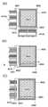
도 3(A) 내지 도 3(C)에 도시된 트랜지스터(430)는 보텀 게이트 구조의 하나인 역 스태거형 트랜지스터라고도 하는 트랜지스터의 일례다. 도 3(A)는 트랜지스터(430)의 평면도이고, 도 3(B)는 도 3(A)의 C1-C2를 따라 절단한 단면도(채널 길이 방향의 단면도)이고, 도 3(C)는 도 3(A)의 D1-D2를 따라 절단한 단면도(채널 폭 방향의 단면도)다. 또한, 도 3(A)에서 L은 채널 길이를 나타내고, W는 채널 폭을 나타낸다. 또한, 도 3(A)에서는 복잡화를 피하기 위하여 트랜지스터(430)의 구성 요소의 일부(예를 들어 게이트 절연막(402) 등)를 생략하였다.The
도 3(A) 내지 도 3(C)에 도시된 바와 같이, 트랜지스터(430)를 포함한 반도체 장치는 절연 표면을 갖는 기판(400) 위에 게이트 전극층(401), 게이트 절연막(402), 산화물 반도체막(403), 소스 전극층(405a), 및 드레인 전극층(405b)을 갖는다. 또한, 트랜지스터(430)를 덮는 절연막(407)이 형성되어 있다.3 (A) to 3 (C), a semiconductor device including a
도 3(A) 내지 도 3(C)에 도시된 트랜지스터(430)에서도 산화물 반도체막(403)과 절연막(407)의 계면에서의 할로겐 원소 농도(예를 들어 염소 농도)는 5×10¹⁸atoms/cm3 이하, 바람직하게는 1×10¹⁸atoms/cm3 이하로 저감되어 있다. 이로써, 트랜지스터의 백 채널의 저저항화(n형화)가 억제되어 기생 채널이 형성되는 것이 억제된 트랜지스터(430)로 할 수 있다. 따라서, 트랜지스터(430)의 고신뢰성화를 도모할 수 있다.The halogen element concentration (for example, the chlorine concentration) at the interface between the
또한, 도 3(A) 내지 도 3(C)에 도시된 바와 같이, 트랜지스터(430)에서 소스 전극층(405a) 및 드레인 전극층(405b)의 폭은 산화물 반도체막(403)의 채널 폭 W보다 짧기 때문에 산화물 반도체막(403)의 단부는 노출되어 있다. 따라서, 소스 전극층(405a) 및 드레인 전극층(405b)을 형성할 때 산화물 반도체막(403)의 일부가 제거될 경우가 있다. 또한, 소스 전극층(405a) 및 드레인 전극층(405b)을 형성한 후, 불순물 제거 공정을 할 때 산화물 반도체막(403)의 일부가 제거될 수 있다. 그 경우에는, 도 3(B) 및 도 3(C)에 도시된 바와 같이, 산화물 반도체막(403)의 일부가 제거됨으로써, 산화물 반도체막(403)에서 소스 전극층(405a) 및 드레인 전극층(405b)과 중첩된 영역의 막 두께는 소스 전극층(405a) 및 드레인 전극층(405b)과 중첩되지 않은 영역의 막 두께보다 크다.3 (A) to 3 (C), the width of the
또한, 산화물 반도체막(403)이 제거되지 않은 경우에는, 도 3(D)에 도시된 바와 같은 트랜지스터(440)가 형성된다. 또한, 트랜지스터(440)에서 채널 길이 L 방향의 단면도(도 3(A)의 C1-C2를 따라 절단한 단면도)는 도 1(B)에 도시된 트랜지스터(410)와 마찬가지다.In addition, when the
다음에, 도 4(A) 내지 도 4(E)에 트랜지스터(430)를 갖는 반도체 장치의 제작 방법의 일례를 도시하였다.Next, an example of a method of manufacturing a semiconductor device having the
우선, 기판(400) 위에 게이트 전극층(이것과 같은 층으로 형성되는 배선을 포함함)이 되는 도전막을 형성한다. 본 실시형태에서는 도전막으로서 스퍼터링법에 의하여 막 두께가 100nm인 텅스텐막을 형성하였다.First, a conductive film to be a gate electrode layer (including wirings formed in the same layer as this) is formed on the
다음에, 포토리소그래피 공정에 의하여 도전막 위에 레지스트 마스크를 형성하고, 선택적으로 에칭하여 게이트 전극층(401)을 형성한다. 게이트 전극층(401)을 형성한 후, 레지스트 마스크를 제거한다.Next, a resist mask is formed on the conductive film by a photolithography process, and the
다음에, 게이트 전극층(401) 위에 게이트 절연막(402)을 형성한다. 본 실시형태에서는 고밀도 플라즈마 CVD법에 의하여 막 두께가 200nm인 산화 질화 실리콘막을 형성한다.Next, a
다음에, 게이트 절연막(402) 위에 산화물 반도체막(403)을 형성한다(도 4(A) 참조). 본 실시형태에서 산화물 반도체막(403)으로서 AC 전원 장치를 갖는 스퍼터링 장치를 사용한 스퍼터링법을 사용하여 막 두께가 35nm인 In-Ga-Zn계 산화물막(IGZO막)을 형성한다. 본 실시형태에서 원자수비가 In:Ga:Zn=1:1:1(=1/3:1/3:1/3)인 In-Ga-Zn계 산화물 타깃을 사용한다. 또한, 성막 조건은 산소 및 아르곤 분위기하(산소 유량 비율이 50%), 압력 0.6Pa, 전원 전력 5kW, 기판 온도 170℃로 한다. 이 성막 조건하에서의 성막 속도는 16nm/min이다.Next, an
산화물 반도체막(403)에 과잉 수소(물이나 수산기를 포함함)를 제거(탈수화 또는 탈수소화)하기 위한 가열 처리를 하여도 좋다. 본 실시형태에서는 가열 처리 장치의 하나인 전기로에 기판을 도입하고, 산화물 반도체막(403)에 질소 분위기하에서 450℃로 1시간 동안의 가열 처리 및 질소 및 산소 분위기하에서 450℃로 1시간 동안의 가열 처리를 한다.The
다음에, 게이트 전극층(401), 게이트 절연막(402), 산화물 반도체막(403) 위에 소스 전극층 및 드레인 전극층(이것과 같은 층으로 형성되는 배선을 포함함)이 되는 도전막(445)을 형성한다(도 4(B) 참조). 본 실시형태에서는 스퍼터링법에 의하여 막 두께가 100nm인 티타늄막, 막 두께가 400nm인 알루미늄막, 막 두께가 100nm인 티타늄막을 적층하고, 드라이 에칭법에 의하여 티타늄막, 알루미늄막, 티타늄막의 적층을 에칭하여 소스 전극층(405a) 및 드레인 전극층(405b)을 형성한다.Next, on the
또한, 본 실시형태에서는 소스 전극층(405a) 및 드레인 전극층(405b)은 산화물 반도체막(403)의 채널 폭 W보다 짧기 때문에 산화물 반도체막(403)의 단부는 노출되어 있다. 따라서, 도전막(445)의 에칭 공정을 할 때 산화물 반도체막(403)이 에칭되어 소실되거나 분단되지 않도록 도전막(445)의 에칭 조건을 최적화하는 것이 요구된다. 그러나, 산화물 반도체막(403)이 전혀 에칭되지 않고 도전막(445)만이 에칭되는 조건을 얻기 어렵기 때문에 도전막(445)을 에칭할 때 산화물 반도체막(403)의 일부가 제거될 경우가 있다. 이 경우에는, 산화물 반도체막(403)의 일부가 제거됨으로써 산화물 반도체막(403)에서 소스 전극층(405a) 및 드레인 전극층(405b)과 중첩된 영역의 막 두께는 소스 전극층(405a) 및 드레인 전극층(405b)과 중첩되지 않은 영역의 막 두께보다 크다.In the present embodiment, since the
소스 전극층(405a) 및 드레인 전극층(405b)을 형성하기 위한 에칭 공정에서 할로겐 원소를 함유한 에칭 가스를 사용하는 경우에는, 산화물 반도체막(403)이 상기 에칭 가스에 폭로되면, 상기 에칭 가스에 함유된 할로겐 원소(예를 들어 염소나 불소)에 의하여 산화물 반도체막(403) 내의 산소가 뽑아져 산화물 반도체막(403) 표면에 산소 결손이 생길 우려가 있다. 산화물 반도체막(403)에 산소 결손이 생기면, 산화물 반도체막(403)의 백 채널이 저저항화(n형화)되어 기생 채널이 형성될 우려가 있다.In the case where an etching gas containing a halogen element is used in the etching process for forming the
또한, 할로겐 원소를 함유한 에칭 가스에는 할로겐 외의 원소(예를 들어 붕소)도 함유되기 때문에, 산화물 반도체막(403)의 백 채널 측이 저저항화되는 요인의 하나가 될 수 있다.Further, since the etching gas containing a halogen element also contains an element (for example, boron) other than a halogen, the back channel side of the
본 실시형태에서는 소스 전극층(405a) 및 드레인 전극층(405b)을 형성하기 위한 에칭 공정에서 할로겐 원소를 함유한 가스(447)를 사용하기 때문에 생기는 불순물은 할로겐(본 실시형태에서는 염소)계 불순물(할로겐 원소 또는 할로겐 화합물)이 된다. 또한, 본 실시형태와 같이, 할로겐 원소를 함유한 가스(447)에 붕소가 함유된 경우에는, 생기는 불순물로서 붕소 또는 붕소를 함유한 화합물도 포함된다.In the present embodiment, the impurity generated by using the halogen-containing
그래서, 소스 전극층(405a) 및 드레인 전극층(405b)을 형성한 후, 산화물 반도체막(403) 표면 및 표면 근방에 존재하는 불순물을 제거하는 공정을 한다(도 4(D) 참조). 불순물 제거 공정은 산소, 일산화 이질소, 또는 희가스(대표적으로는 아르곤)를 사용한 플라즈마 처리, 또는 희석된 불산, 물, 현상액, 또는 TMAH 용액을 사용한 용액 처리 등을 적합하게 사용할 수 있다. 또한, 희석된 불산으로서 예를 들어 1/103으로 희석된 불산(불산: 0.05%)으로 IGZO막을 처리하면, 막 두께가 1초당 1nm 내지 3nm 감소되고, 2/105로 희석된 불산(불산: 0.0025%)으로 IGZO막을 처리하면, 막 두께가 1초당 0.1nm 정도 감소된다. 산화물 반도체막(403)에 불순물 제거 처리를 함으로써 산화물 반도체막(403) 표면에서의 할로겐 원소 농도(예를 들어 염소 농도)를 5×10¹⁸atoms/cm3 이하, 바람직하게는 1×10¹⁸atoms/cm3 이하로 저감시킬 수 있다. 본 실시형태에서는 불순물 제거 공정으로서 1/103으로 희석된 불산을 사용한 용액 처리를 하는 예를 기재한다.Thus, after forming the
또한, 불순물 제거 공정에서 산화물 반도체막(403)이 에칭되어 분단되거나 소실되지 않도록 불순물 제거 공정의 조건을 최적화하는 것이 요구된다. 그러나, 산화물 반도체막(403)이 전혀 제거되지 않는 조건을 얻기 어렵기 때문에 산화물 반도체막(403)이 노출된 부분에서 일부가 제거되어 산화물 반도체막(403)이 홈부(오목부)를 갖는 경우도 있다. 도 4(D)는 불순물 제거 공정 후, 산화물 반도체막(403)이 부분적으로 제거되어 산화물 반도체막(403)이 홈부(오목부)를 갖는 경우를 도시한 것이다. 도 4(D)에 도시된 바와 같이, 소스 전극층(405a) 및 드레인 전극층(405b)과 중첩된 영역의 막 두께는 소스 전극층(405a) 및 드레인 전극층(405b)과 중첩되지 않은 영역의 막 두께보다 크다. 또한, 채널 폭 W 방향을 따라 절단한 단면도는 도 3(C)의 단면도를 참조하면 좋다.In addition, it is required to optimize the conditions of the impurity removal process so that the
상술한 공정을 거쳐 본 실시형태의 트랜지스터(430)가 제작된다(도 4(E) 참조).Through the above-described processes, the
본 실시형태에서는 소스 전극층(405a) 및 드레인 전극층(405b) 위에 산화물 반도체막(403)과 접촉되도록 보호 절연막이 되는 절연막(407)을 형성한다. 예를 들어 CVD법에 의하여 형성한 산화 질화 실리콘막을 막 두께 400nm로 형성한다. 또한, 보호 절연막을 형성한 후에 가열 처리하여도 좋다. 예를 들어 질소 분위기하에서 300℃로 1시간 동안 가열 처리한다.The insulating
또한, 트랜지스터(430)에 기인한 표면 요철을 저감시키기 위하여 평탄화 절연막(408)을 형성하여도 좋다.In addition, a
예를 들어 보호 절연막 위에 평탄화 절연막(408)으로서 막 두께가 1500nm인 아크릴 수지막을 형성하면 좋다. 아크릴 수지막은 도포법에 의한 도포 후에 소성(燒成)(예를 들어 질소 분위기하에서 250℃로 1시간 동안)하여 형성할 수 있다.For example, an acrylic resin film having a film thickness of 1500 nm may be formed as a
평탄화 절연막을 형성한 후에 가열 처리하여도 좋다. 예를 들어 질소 분위기하에서 250℃로 1시간 동안 가열 처리한다.The planarizing insulating film may be formed and then heat-treated. For example, at 250 DEG C for 1 hour in a nitrogen atmosphere.
상술한 바와 같이, 불순물 제거 공정을 함으로써 산화물 반도체막(403)의 표면 및 표면 근방에 불순물이 잔존하는 것을 방지할 수 있다. 따라서, 트랜지스터(430)는 산화물 반도체막(403) 표면에서의 에칭 공정에 기인한 불순물(대표적으로는 할로겐 원소(예를 들어 염소나 불소), 붕소, 또는 붕소를 함유한 화합물)의 농도가 저감된다. 또한, 산화물 반도체막(403)과 절연막(407)의 계면에서 에칭 공정에 기인한 불순물(대표적으로는 할로겐(예를 들어 염소나 불소), 붕소, 인, 알루미늄, 철, 또는 탄소)의 농도를 5×10¹⁸atoms/cm3 이하(바람직하게는 1×10¹⁸atoms/cm3 이하)로 할 수 있다.As described above, it is possible to prevent impurities from remaining on the surface and in the vicinity of the surface of the
따라서, 산화물 반도체막(403)을 사용함으로써 안정된 전기 특성을 갖는 트랜지스터(430)를 포함한 신뢰성이 높은 반도체 장치를 제공할 수 있다. 또한, 신뢰성이 높은 반도체 장치가 좋은 수율로 제작되어 고생산화를 달성할 수 있다.Therefore, by using the
(실시형태 3)(Embodiment 3)
실시형태 1 또는 실시형태 2에 기재된 트랜지스터를 사용하여 표시 기능을 갖는 반도체 장치(표시 장치라고도 함)를 제작할 수 있다. 또한, 트랜지스터를 포함하는 구동 회로의 일부 또는 전체를 화소부와 동일 기판 위에 일체로 형성하여 시스템 온 패널을 형성할 수 있다.A semiconductor device (also referred to as a display device) having a display function can be manufactured by using the transistor described in Embodiment 1 or 2. [ In addition, a part or the whole of the driver circuit including the transistor may be integrally formed on the same substrate as the pixel portion to form a system-on-panel.
도 5(A)에서 제 1 기판(4001) 위에 형성된 화소부(4002)를 둘러싸도록 씰재(4005)가 형성되고, 화소부(4002)는 제 2 기판(4006)에 의하여 밀봉되어 있다. 도 5(A)에서는 제 1 기판(4001) 위의 씰재(4005)에 의하여 둘러싸여 있는 영역과 다른 영역에 별도 준비된 기판 위에 단결정 반도체막 또는 다결정 반도체막으로 형성된 주사선 구동 회로(4004), 신호선 구동 회로(4003)가 실장되어 있다. 또한, 별도 형성된 신호선 구동 회로(4003) 및 주사선 구동 회로(4004), 또는 화소부(4002)에는 FPC(Flexible printed circuit)(4018a, 4018b)로부터 각종 신호 및 전위가 공급된다.5A, a sealing
도 5(B) 및 도 5(C)에서 제 1 기판(4001) 위에 형성된 화소부(4002)와 주사선 구동 회로(4004)를 둘러싸도록 씰재(4005)가 형성되어 있다. 또한, 화소부(4002)와 주사선 구동 회로(4004) 위에 제 2 기판(4006)이 형성되어 있다. 따라서, 화소부(4002)와 주사선 구동 회로(4004)는 제 1 기판(4001)과 씰재(4005)와 제 2 기판(4006)에 의하여 표시 소자와 함께 밀봉되어 있다. 도 5(B) 및 도 5(C)에서는 제 1 기판(4001) 위의 씰재(4005)에 의하여 둘러싸여 있는 영역과 다른 영역에 별도 준비된 기판 위에 단결정 반도체막 또는 다결정 반도체막으로 형성된 신호선 구동 회로(4003)가 실장되어 있다. 도 5(B) 및 도 5(C)에서는 신호선 구동 회로(4003)와, 주사선 구동 회로(4004) 또는 화소부(4002)에 FPC(4018)로부터 각종 신호 및 전위가 공급된다.A sealing
또한, 도 5(B) 및 도 5(C)에서는 신호선 구동 회로(4003)를 별도 형성하고 제 1 기판(4001)에 실장한 예를 도시하였지만, 이 구성에 한정되지 않는다. 주사선 구동 회로를 별도 형성하고 실장하여도 좋고, 신호선 구동 회로의 일부 또는 주사선 구동 회로의 일부만을 별도 형성하고 실장하여도 좋다.5B and 5C show an example in which the signal
또한, 별도 형성한 구동 회로의 접속 방법은 특별히 한정되지 않고, COG(Chip On Glass) 방법, 와이어 본딩 방법, 또는 TAB(Tape Automated Bonding) 방법 등을 사용할 수 있다. 도 5(A)는 COG 방법에 의하여 신호선 구동 회로(4003) 및 주사선 구동 회로(4004)를 실장한 예이며, 도 5(B)는 COG 방법에 의하여 신호선 구동 회로(4003)를 실장한 예이며, 도 5(C)는 TAB 방법에 의하여 신호선 구동 회로(4003)를 실장한 예이다.The connection method of the separately formed drive circuit is not particularly limited, and a COG (Chip On Glass) method, a wire bonding method, a TAB (Tape Automated Bonding) method, or the like can be used. 5A is an example in which the signal
또한, 표시 장치란 표시 소자가 밀봉된 상태인 패널과, 상기 패널에 컨트롤러를 포함한 IC 등이 실장된 상태인 모듈을 포함한다.The display device includes a panel in which a display element is sealed, and a module in which an IC or the like including a controller is mounted on the panel.
즉 본 명세서의 표시 장치란 화상 표시 디바이스, 표시 디바이스, 또는 광원(조명 장치를 포함함)을 가리킨다. 또한, 커넥터 예를 들어 FPC, TAB 테이프, 또는 TCP가 장착된 모듈, TAB 테이프나 TCP 끝에 프린트 배선판이 형성된 모듈, 또는 표시 소자에 COG 방식에 의하여 IC(집적 회로)가 직접 실장된 모듈도 모두 표시 장치에 포함하는 것으로 한다.That is, the display device in the present specification refers to an image display device, a display device, or a light source (including a lighting device). Also, all of the connectors, for example, a module in which an FPC, a TAB tape, or a TCP module, a TAB tape, a module in which a printed wiring board is formed at the end of a TCP, or a module in which an IC (integrated circuit) Device.
또한, 제 1 기판 위에 형성된 화소부 및 주사선 구동 회로는 복수의 트랜지스터를 갖고, 실시형태 1 또는 실시형태 2에 기재된 트랜지스터를 적용할 수 있다.Further, the pixel portion formed on the first substrate and the scanning line driving circuit have a plurality of transistors, and the transistors described in Embodiment Mode 1 or Embodiment Mode 2 can be applied.
표시 장치에 형성되는 표시 소자로서는 액정 소자(액정 표시 소자라고도 함), 발광 소자(발광 표시 소자라고도 함)를 사용할 수 있다. 발광 소자는 전류 또는 전압에 의하여 휘도가 제어되는 소자를 그 범주에 포함하고, 구체적으로는 무기 EL(Electro Luminescence), 유기 EL 등이 포함된다. 또한, 전자 잉크 등, 전기적 작용에 의하여 콘트라스트가 변화되는 표시 매체도 적용할 수 있다.As the display element formed on the display device, a liquid crystal element (also referred to as a liquid crystal display element) or a light emitting element (also referred to as a light emitting display element) can be used. The light-emitting element includes an element whose luminance is controlled by a current or a voltage, and specifically includes an inorganic EL (Electro Luminescence), an organic EL, and the like. Further, a display medium in which the contrast is changed by an electrical action such as electronic ink can also be applied.
또한, 반도체 장치의 일 형태에 대하여 도 5(A) 내지 도 7(B)를 사용하여 설명한다. 도 7(A) 및 도 7(B)는 도 5(B)의 1점 쇄선 M-N을 따라 절단한 단면도에 상당한다.One embodiment of the semiconductor device will be described with reference to Figs. 5 (A) to 7 (B). Figs. 7A and 7B correspond to cross-sectional views taken along one-dot chain line M-N in Fig. 5B.
도 5(A) 내지 도 7(B)에 도시된 바와 같이, 반도체 장치는 접속 단자 전극(4015) 및 단자 전극(4016)을 갖고, 접속 단자 전극(4015) 및 단자 전극(4016)은 이방성 도전막(4019)을 통하여 FPC(4018) 및 FPC(4018b)가 갖는 단자와 전기적으로 접속되어 있다.5A to 7B, the semiconductor device has a
접속 단자 전극(4015)은 제 1 전극층(4030)과 같은 도전막으로 형성되고, 단자 전극(4016)은 트랜지스터(4010) 및 트랜지스터(4011)의 게이트 전극과 같은 도전막으로 형성되어 있다.The
또한, 제 1 기판(4001) 위에 형성된 화소부(4002) 및 주사선 구동 회로(4004)는 복수의 트랜지스터를 갖고, 도 7(A) 및 도 7(B)에는 화소부(4002)에 포함되는 트랜지스터(4010)와 주사선 구동 회로(4004)에 포함되는 트랜지스터(4011)를 예시하였다. 도 7(A)에서는 트랜지스터(4010) 및 트랜지스터(4011) 위에 절연막(4020)이 형성되어 있고, 도 7(B)에서는 절연막(4020) 위에 절연막(4021)이 더 형성되어 있다.The
트랜지스터(4010) 및 트랜지스터(4011)로서 실시형태 1 또는 실시형태 2에 기재된 트랜지스터를 적용할 수 있다. 본 실시형태에서는 실시형태 1에 기재된 트랜지스터(410)와 같은 구조를 갖고 같은 제작 방법으로 얻어지는 트랜지스터를 적용하는 예를 기재한다.As the
실시형태 1에 기재된 트랜지스터(410)와 같은 구조를 갖고 같은 제작 방법으로 얻어지는 트랜지스터(4010) 및 트랜지스터(4011)는 할로겐 원소를 함유한 에칭 가스를 사용한 에칭 공정에 의하여 소스 전극층 및 드레인 전극층을 형성한 후, 산화물 반도체막 표면 및 표면 근방에서 에칭 가스에 함유된 불순물을 제거하는 공정을 한다. 불순물 제거 공정으로서는 예를 들어 희석된 불산을 사용한 처리 또는 산소나 일산화 이질소를 사용한 플라즈마 처리 등을 적합하게 사용할 수 있다.The
산화물 반도체막 표면 및 표면 근방이 에칭 가스에 함유된 불순물로 오염되는 것을 방지할 수 있기 때문에 트랜지스터(4010) 및 트랜지스터(4011)는 산화물 반도체막 표면에서의 할로겐 원소의 농도를 5×10¹⁸atoms/cm3 이하(바람직하게는 1×10¹⁸atoms/cm3 이하)로 할 수 있다.The oxide semiconductor layer surface and the surface vicinity is because it can be prevented from being contaminated with impurities contained in the etching gas, the
따라서, 도 5(A) 내지 도 5(C) 및 도 7(A) 및 도 7(B)에 도시된 본 실시형태의 산화물 반도체막을 사용함으로써 안정된 전기 특성을 갖는 트랜지스터(4010) 및 트랜지스터(4011)를 포함한 신뢰성이 높은 반도체 장치를 제공할 수 있다. 또한, 이러한 신뢰성이 높은 반도체 장치가 좋은 수율로 제작되어 고생산화를 달성할 수 있다.Therefore, by using the oxide semiconductor film of this embodiment shown in Figs. 5A to 5C and Figs. 7A and 7B, the
또한, 구동 회로용 트랜지스터(4011)의 산화물 반도체막의 채널 형성 영역과 중첩된 위치에 도전층을 더 형성하여도 좋다. 도전층을 산화물 반도체막의 채널 형성 영역과 중첩된 위치에 형성함으로써, 바이어스-열 스트레스 시험(BT 시험) 전후에서의 트랜지스터(4011)의 임계값 전압의 변화량을 더 저감시킬 수 있다. 또한, 도전층은 전위가 트랜지스터(4011)의 게이트 전극층의 전위와 동일하여도 좋고 달라도 좋고, 제 2 게이트 전극층으로서 기능시킬 수도 있다. 또한, 도전층의 전위는 GND, 0V, 또는 부유 상태라도 좋다.Further, a conductive layer may be further formed at a position overlapping with the channel forming region of the oxide semiconductor film of the
또한, 상기 도전층은 외부의 전기장을 차폐하는 기능 즉 외부의 전기장이 내부(트랜지스터를 포함하는 회로부)에 작용하지 않도록 하는 기능(특히, 정전기에 대한 정전 차폐 기능)도 갖는다. 도전층의 차폐 기능에 의하여 정전기 등 외부의 전기장의 영향으로 트랜지스터의 전기적 특성이 변동하는 것을 방지할 수 있다.The conductive layer also has a function of shielding an external electric field, that is, a function of preventing an external electric field from acting on the inside (a circuit portion including a transistor) (in particular, an electrostatic shielding function against static electricity). The shielding function of the conductive layer can prevent the electrical characteristics of the transistor from fluctuating due to the influence of an external electric field such as static electricity.
화소부(4002)에 형성된 트랜지스터(4010)는 표시 소자와 전기적으로 접속되어 표시 패널을 구성한다. 표시 소자는 표시를 할 수 있는 것이면 특별히 한정되지 않고 다양한 표시 소자를 사용할 수 있다.A
도 7(A)에 표시 소자로서 액정 소자를 사용한 액정 표시 장치의 예를 도시하였다. 도 7(A)에서 표시 소자인 액정 소자(4013)는 제 1 전극층(4030), 제 2 전극층(4031), 및 액정층(4008)을 포함한다. 또한, 배향막으로서 기능하는 절연막(4032) 및 절연막(4033)이 액정층(4008)을 협지하도록 제공되어 있다. 제 2 전극층(4031)은 제 2 기판(4006) 측에 제공되고, 제 1 전극층(4030)과 제 2 전극층(4031)은 액정층(4008)을 개재하여 적층되어 있다.Fig. 7A shows an example of a liquid crystal display device using a liquid crystal element as a display element. 7A, a
또한, 스페이서(4035)는 절연막을 선택적으로 에칭함으로써 얻어지는 기둥 형상의 스페이서이며, 액정층(4008)의 막 두께(셀 갭)를 제어하기 위하여 제공되어 있다. 또한, 구(球) 형상의 스페이서를 사용하여도 좋다.The
표시 소자로서 액정 소자를 사용하는 경우에는, 서모트로픽 액정, 저분자 액정, 고분자 액정, 고분자 분산형 액정, 강유전성 액정, 반강유전성 액정 등을 사용할 수 있다. 이들 액정 재료(액정 조성물)는 조건에 따라 콜레스테릭(cholesteric)상, 스멕틱상, 큐빅상, 키랄네마틱상, 등방상 등을 나타낸다.When a liquid crystal element is used as a display element, a thermotropic liquid crystal, a low molecular liquid crystal, a polymer liquid crystal, a polymer dispersed liquid crystal, a ferroelectric liquid crystal, an antiferroelectric liquid crystal, or the like can be used. These liquid crystal materials (liquid crystal compositions) exhibit a cholesteric phase, a smectic phase, a cubic phase, a chiral nematic phase, an isotropic phase and the like depending on conditions.
또한, 액정층(4008)에 배향막을 사용하지 않는 블루상을 발현하는 액정 조성물을 사용하여도 좋다. 이 경우에는, 액정층(4008)과, 제 1 전극층(4030) 및 제 2 전극층(4031)이 접촉된 구조가 된다. 블루상은 액정상의 하나이며, 콜레스테릭 액정을 계속하여 승온하면, 콜레스테릭상으로부터 등방상으로 전이하기 직전에 발현하는 상이다. 블루상은 액정 및 키랄제를 혼합시킨 액정 조성물을 사용하여 발현할 수 있다. 또한, 블루상이 발현되는 온도 범위를 넓히기 위하여 블루상을 발현하는 액정 조성물에 중합성 단량체 및 중합 개시제 등을 첨가하여 고분자 안정화시키는 처리를 하여 액정층을 형성할 수도 있다. 블루상을 발현하는 액정 조성물은 응답 시간이 짧고, 광학적 등방성이기 때문에 배향 처리가 불필요하고, 시야각 의존성이 작다. 또한, 배향막을 제공할 필요가 없어 러빙 처리도 불필요하기 때문에 러빙 처리로 인한 정전 파괴를 방지할 수 있어 제작 공정 도중에 일어나는 액정 표시 장치의 불량이나 파손을 경감할 수 있다. 따라서, 액정 표시 장치의 생산성을 향상시킬 수 있다. 산화물 반도체막을 사용하는 트랜지스터는 정전기의 영향에 의하여 트랜지스터의 전기적인 특성이 현저하게 변동하여 설계 범위를 일탈할 우려가 있다. 따라서, 산화물 반도체막을 사용하는 트랜지스터를 갖는 액정 표시 장치에 블루상을 발현하는 액정 조성물을 사용하는 것은 더 효과적이다.Further, a liquid crystal composition which exhibits a blue phase without using an alignment film may be used for the
또한, 액정 재료의 고유 저항은 1×10⁹Ω·cm 이상이고, 바람직하게는 1×10¹¹Ω·cm 이상, 더 바람직하게는 1×10¹²Ω·cm 이상이다. 또한, 본 명세서에서의 고유 저항의 값은 20℃로 측정한 값으로 한다.Further, the intrinsic resistance of the liquid crystal material is 1 x 10⁹ ? · Cm or more, preferably 1 x 10¹¹ ? · Cm or more, and more preferably 1 x 10¹² ? · Cm or more. In addition, the value of the intrinsic resistance in this specification is a value measured at 20 占 폚.
액정 표시 장치에 제공되는 유지 용량의 크기는 화소부에 배치되는 트랜지스터의 누설 전류 등을 고려하여 소정 기간 동안 전하를 유지할 수 있도록 설정된다. 유지 용량의 크기는 트랜지스터의 오프 전류 등을 고려하여 설정하면 좋다. 본 명세서에 기재되는 산화물 반도체막을 갖는 트랜지스터를 사용함으로써, 각 화소의 액정 용량의 1/3 이하, 바람직하게는 1/5 이하의 용량을 갖는 유지 용량을 제공하면 충분하다.The size of the holding capacitor provided in the liquid crystal display device is set so as to maintain the charge for a predetermined period in consideration of the leakage current of the transistor disposed in the pixel portion. The size of the holding capacitor may be set in consideration of the off current of the transistor and the like. By using a transistor having an oxide semiconductor film described in this specification, it is sufficient to provide a storage capacitor having a capacity of 1/3 or less, preferably 1/5 or less of the liquid crystal capacitance of each pixel.
본 명세서에 기재되는 산화물 반도체막을 사용한 트랜지스터는 오프 상태에서의 전류값(오프 전류값)을 낮게 제어할 수 있다. 따라서, 화상 신호 등의 전기 신호의 유지 시간을 길게 할 수 있고 전원이 온 된 상태에서는 기록 간격도 길게 설정할 수 있다. 따라서, 리프레시 동작의 빈도를 적게 할 수 있기 때문에 소비 전력을 억제하는 효과를 나타낸다.The transistor using the oxide semiconductor film described in this specification can control the current value (off current value) in the OFF state to be low. Therefore, the holding time of an electric signal such as an image signal can be lengthened, and the recording interval can also be set longer when the power is turned on. Therefore, since the frequency of the refresh operation can be reduced, the power consumption is suppressed.
또한, 본 명세서에 기재되는 산화물 반도체막을 사용한 트랜지스터는 비교적 높은 전계 효과 이동도를 가질 수 있기 때문에 고속 구동이 가능하다. 예를 들어 이러한 고속 구동이 가능한 트랜지스터를 액정 표시 장치에 사용함으로써, 화소부의 스위칭 트랜지스터와 구동 회로부에 사용하는 드라이버 트랜지스터를 동일 기판 위에 형성할 수 있다. 즉 구동 회로로서 실리콘 웨이퍼 등으로 형성된 반도체 장치를 별도 사용할 필요가 없기 때문에, 반도체 장치의 부품 개수를 삭감할 수 있다. 또한, 화소부에서도 고속 구동이 가능한 트랜지스터를 사용함으로써 고화질 화상을 제공할 수 있다.In addition, since the transistor using the oxide semiconductor film described in this specification can have a relatively high field effect mobility, high-speed driving is possible. For example, by using such a transistor capable of high-speed driving in a liquid crystal display device, a switching transistor of the pixel portion and a driver transistor used for the driving circuit portion can be formed on the same substrate. In other words, since it is not necessary to separately use a semiconductor device formed of a silicon wafer or the like as the drive circuit, the number of parts of the semiconductor device can be reduced. In addition, a high-quality image can be provided by using a transistor capable of high-speed driving in the pixel portion.
액정 표시 장치에는 TN(Twisted Nematic) 모드, IPS(In-Plane-Switching) 모드, FFS(Fringe Field Switching) 모드, ASM(Axially Symmetric aligned Micro-cell) 모드, OCB(Optical Compensated Birefringence) 모드, FLC(Ferroelectric Liquid Crystal) 모드, AFLC(AntiFerroelectric Liquid Crystal) 모드 등을 사용할 수 있다.The liquid crystal display device includes a twisted nematic (TN) mode, an in-plane switching (IPS) mode, a fringe field switching (FFS) mode, an axially symmetric aligned micro-cell (ASM) mode, an optical compensated birefringence Ferroelectric liquid crystal (AFLC) mode, and AFLC (anti-ferroelectric liquid crystal) mode.
또한, 노멀리 블랙형 액정 표시 장치 예를 들어 수직 배향(VA) 모드를 채용한 투과형 액정 표시 장치로 하여도 좋다. 수직 배향 모드로서는 몇 가지 들 수 있지만, 예를 들어 MVA(Multi-Domain Vertical Alignment) 모드, PVA(Patterned Vertical Alignment) 모드, ASV(Advanced Super View) 모드 등을 사용할 수 있다. 또한, VA형 액정 표시 장치에 적용할 수도 있다. VA형 액정 표시 장치란 액정 표시 패널의 액정 분자의 배열을 제어하는 방식의 하나다. VA형 액정 표시 장치는 전압이 인가되지 않을 때 액정 분자가 패널 면에 대하여 수직 방향을 향하는 방식이다. 또한, 화소(픽셀)를 몇 개의 영역(서브 픽셀)으로 나누고 각각 다른 방향으로 분자가 배향되도록 구성되는 멀티 도메인화 또는 멀티 도메인 설계라고 하는 방법을 사용할 수 있다.Alternatively, a normally black type liquid crystal display device, for example, a transmissive liquid crystal display device employing a vertically aligned (VA) mode may be used. There are several vertical alignment modes. For example, a multi-domain vertical alignment (MVA) mode, a patterned vertical alignment (PVA) mode, and an advanced super view (ASV) mode can be used. The present invention can also be applied to a VA type liquid crystal display device. The VA type liquid crystal display device is a method of controlling the arrangement of liquid crystal molecules in a liquid crystal display panel. The VA type liquid crystal display apparatus is a system in which liquid crystal molecules are oriented in a direction perpendicular to the panel surface when no voltage is applied. Also, a method of multi-domainization or multi-domain design, in which pixels (pixels) are divided into several regions (subpixels) and molecules are oriented in different directions, respectively, can be used.
또한, 표시 장치에서 블랙 매트릭스(차광층), 편광 부재, 위상차 부재, 반사 방지 부재 등의 광학 부재(광학 기판) 등은 적절히 형성한다. 예를 들어 편광 기판 및 위상차 기판에 의한 원 편광을 사용하여도 좋다. 또한, 광원으로서 백 라이트나 사이드 라이트 등을 사용하여도 좋다.Further, an optical member (optical substrate) such as a black matrix (light-shielding layer), a polarizing member, a retardation member, an antireflection member, or the like is appropriately formed in the display device. For example, circularly polarized light by a polarizing substrate and a phase difference substrate may be used. Further, a backlight or a sidelight may be used as the light source.
또한, 화소부에서의 표시 방식은 프로그레시브 방식이나 인터레이스 방식 등을 사용할 수 있다. 또한, 컬러 표시하는 경우에는, 화소에서 제어하는 색 요소는 RGB(R는 적색, G는 녹색, B는 청색을 나타냄)의 3색에 한정되지 않는다. 예를 들어 RGBW(W는 백색을 나타냄) 또는 RGB에 옐로, 시안, 마젠타 등 중 하나 이상을 추가한 것이 있다. 또한, 색 요소의 도트마다 그 표시 영역의 크기가 달라도 좋다. 다만, 기재하는 발명은 컬러 표시의 표시 장치에 한정되지 않고, 흑백 표시의 표시 장치에 적용할 수도 있다.The display method in the pixel portion can use a progressive method, an interlace method, or the like. Further, in the case of color display, the color element controlled by the pixel is not limited to three colors of RGB (R represents red, G represents green, and B represents blue). For example, RGBW (W represents white) or RGB is added to at least one of yellow, cyan, magenta, and the like. The size of the display area may be different for each dot of the color element. However, the invention to be described is not limited to the display device for color display, and can also be applied to a display device for monochrome display.
또한, 표시 장치에 포함되는 표시 소자로서 일렉트로루미네선스를 이용하는 발광 소자를 적용할 수 있다. 일렉트로루미네선스를 이용하는 발광 소자는 발광 재료가 유기 화합물인지 무기 화합물인지에 따라 구별되며, 일반적으로 전자는 유기 EL 소자라고 불리고 후자는 무기 EL 소자라고 불린다.Further, a light emitting element using electroluminescence can be applied as a display element included in a display device. The light emitting element using electroluminescence is classified according to whether the light emitting material is an organic compound or an inorganic compound. Generally, the former is called an organic EL element and the latter is called an inorganic EL element.
유기 EL 소자는 발광 소자에 전압을 인가함으로써, 한 쌍의 전극으로부터 전자 및 정공이 각각 발광성의 유기 화합물을 함유한 층에 주입되어 전류가 흐른다. 그리고, 이들 캐리어(전자 및 정공)가 재결합함으로써 발광성 유기 화합물이 여기 상태를 형성하고, 그 여기 상태가 기저 상태로 되돌아올 때에 발광한다. 이러한 메커니즘 때문에 이러한 발광 소자는 전류 여기형 발광 소자라고 불린다. 본 실시형태에서는 발광 소자로서 유기 EL 소자를 사용하는 예를 기재한다.In the organic EL element, electrons and holes from a pair of electrodes are injected into a layer containing a luminescent organic compound by applying a voltage to the luminescent element, and a current flows. Then, these carriers (electrons and holes) recombine to form an excited state of the luminous organic compound, and emits light when the excited state returns to the ground state. Because of this mechanism, such a light emitting element is called a current-excited light emitting element. In this embodiment, an example in which an organic EL element is used as a light emitting element is described.
무기 EL 소자는 그 소자 구성에 따라 분산형 무기 EL 소자와 박막형 무기 EL 소자로 분류된다. 분산형 무기 EL 소자는 발광 재료의 입자를 바인더 중에 분산시킨 발광층을 갖는 것이며, 발광 메커니즘은 도너 준위와 억셉터 준위를 이용하는 도너-억셉터 재결합형 발광이다. 박막형 무기 EL 소자는 발광층을 유전체층 사이에 개재하고 그것을 전극 사이에 개재한 구조를 갖고, 발광 메커니즘은 금속 이온의 내각 전자 전이(轉移)를 이용하는 국재형 발광이다. 또한, 여기서는 발광 소자로서 유기 EL 소자를 사용하여 설명한다.The inorganic EL element is classified into a dispersion type inorganic EL element and a thin film inorganic EL element according to its element structure. The dispersion-type inorganic EL device has a light-emitting layer in which particles of a light-emitting material are dispersed in a binder, and the light-emitting mechanism is a donor-acceptor recombination-type light-emission using a donor level and an acceptor level. The thin film type inorganic EL device has a structure in which a light emitting layer is sandwiched between dielectric layers and interposed between the electrodes, and the light emitting mechanism is a localized light emitting using the internal angle electron transition of metal ions. Here, an organic EL element is used as a light emitting element.
발광 소자는 발광을 추출하기 위하여 적어도 한 쌍의 전극 중 하나가 투광성을 가지면 좋다. 그리고, 기판 위에 트랜지스터 및 발광 소자를 형성하고, 기판과 반대 측의 면으로부터 발광을 추출하는 상면 사출 구조나, 기판 측의 면으로부터 발광을 추출하는 하면 사출 구조나, 기판 측 및 기판과 반대 측의 면으로부터 발광을 추출하는 양면 사출 구조의 발광 소자가 있고, 어느 사출 구조의 발광 소자나 적용할 수 있다.In order to extract light emission, at least one of the pair of electrodes may have a light transmitting property. In addition, a top surface injection structure for forming a transistor and a light emitting element on a substrate and extracting light emission from a surface opposite to the substrate, a bottom injection structure for extracting light emission from the surface on the substrate side, There is a light emitting element of a double-sided injection structure for extracting light emission from a surface, and any light emitting element of an injection structure can be applied.
도 6(A), 도 6(B), 및 도 7(B)에 표시 소자로서 발광 소자를 사용한 발광 장치의 예를 도시하였다.6 (A), 6 (B) and 7 (B) show examples of light emitting devices using light emitting elements as display elements.
도 6(A)는 발광 장치의 평면도이고, 도 6(A)의 1점 쇄선 V1-W1, V2-W2, 및 V3-W3을 따라 절단한 단면이 도 6(B)에 상당한다. 또한, 도 6(A)의 평면도에서는 전계 발광층(542) 및 제 2 전극층(543)은 생략하였다.6A is a plan view of the light emitting device, and a section taken along one-dot chain lines V1-W1, V2-W2, and V3-W3 in Fig. 6A corresponds to Fig. In the plan view of Fig. 6A, the
도 6(A) 및 도 6(B)에 도시된 발광 장치는 기판(500) 위에 트랜지스터(510), 용량 소자(520), 배선층 교차부(530)를 갖고, 트랜지스터(510)는 발광 소자(540)와 전기적으로 접속되어 있다. 또한, 도 6(A) 및 도 6(B)는 기판(500)을 통하여 발광 소자(540)로부터의 빛을 추출하는 하면 사출형 구조를 갖는 발광 장치다.The light emitting device shown in Figs. 6A and 6B has a
트랜지스터(510)로서 실시형태 1 또는 실시형태 2에 기재된 트랜지스터를 적용할 수 있다. 본 실시형태에서는 실시형태 1에 기재된 트랜지스터(410)와 같은 구조를 갖고 같은 제작 방법으로 얻어지는 트랜지스터를 적용하는 예를 기재한다.As the
트랜지스터(510)는 게이트 전극층(511a), 게이트 전극층(511b), 게이트 절연막(502), 산화물 반도체막(512), 소스 전극층 또는 드레인 전극층으로서 기능하는 도전층(513a) 및 도전층(513b)을 포함한다.The
실시형태 1에 기재된 트랜지스터(410)와 같은 구조를 갖고 같은 제작 방법으로 얻어지는 트랜지스터(510)는 할로겐 원소를 함유한 에칭 가스를 사용한 에칭 공정에 의하여 소스 전극층 또는 드레인 전극층으로서 기능하는 도전층(513a) 및 도전층(513b)을 형성한 후, 산화물 반도체막 표면 및 표면 근방에서 에칭 가스에 함유된 불순물을 제거하는 공정을 한다. 불순물 제거 공정은 예를 들어 희석된 불산을 사용한 처리, 또는 산소나 일산화 이질소를 사용한 플라즈마 처리 등을 적합하게 사용할 수 있다.The
산화물 반도체막 표면 및 표면 근방이 에칭 가스에 함유된 불순물로 오염되는 것을 방지할 수 있기 때문에 트랜지스터(510)는 산화물 반도체막 표면에서의 할로겐 원소의 농도를 5×10¹⁸atoms/cm3 이하(바람직하게는 1×10¹⁸atoms/cm3 이하)로 할 수 있다.Oxide, since the semiconductor film surface, and the surface vicinity can be prevented from being contaminated with impurities contained in the etching gas, the
따라서, 도 6(A) 및 도 6(B)에 도시된 본 실시형태의 산화물 반도체막(512)을 사용함으로써 안정된 전기 특성을 갖는 트랜지스터(510)를 포함한 신뢰성이 높은 반도체 장치를 제공할 수 있다. 또한, 이러한 신뢰성이 높은 반도체 장치가 좋은 수율로 제작되어 고생산화를 달성할 수 있다.Therefore, by using the
용량 소자(520)는 도전층(521a), 도전층(521b), 게이트 절연막(502), 산화물 반도체막(522), 도전층(523)을 포함하고, 도전층(521a) 및 도전층(521b)과 도전층(523)으로 게이트 절연막(502) 및 산화물 반도체막(522)을 끼우는 구성으로 함으로써 용량을 형성한다.The
배선층 교차부(530)는 게이트 전극층(511a) 및 게이트 전극층(511b)과 도전층(533)의 교차부이고, 게이트 전극층(511a) 및 게이트 전극층(511b)과 도전층(533)은 게이트 절연막(502)을 사이에 개재하여 교차한다.The
본 실시형태에서는 게이트 전극층(511a) 및 도전층(521a)으로서 막 두께가 30nm인 티타늄막을 사용하고, 게이트 전극층(511b) 및 도전층(521b)으로서 막 두께가 200nm인 구리 박막을 사용한다. 따라서, 게이트 전극층은 티타늄막과 구리 박막의 적층 구조가 된다.A titanium film having a thickness of 30 nm is used for the
산화물 반도체막(512), 산화물 반도체막(522)으로서는 막 두께가 25nm인 IGZO막을 사용한다.As the
트랜지스터(510), 용량 소자(520), 및 배선층 교차부(530) 위에는 층간 절연막(504)이 형성되고, 층간 절연막(504) 위에서 발광 소자(540)와 중첩된 영역에 컬러 필터층(505)이 형성되어 있다. 층간 절연막(504) 및 컬러 필터층(505) 위에는 평탄화 절연막으로서 기능하는 절연막(506)이 형성되어 있다.An interlayer insulating
절연막(506) 위에 제 1 전극층(541), 전계 발광층(542), 제 2 전극층(543)의 순서로 적층한 적층 구조를 포함한 발광 소자(540)가 형성되어 있다. 도전층(513a)에 도달되는 절연막(506) 및 층간 절연막(504)에 형성된 개구에서 제 1 전극층(541) 및 도전층(513a)이 접촉됨으로써 발광 소자(540)와 트랜지스터(510)는 전기적으로 접속되어 있다. 또한, 제 1 전극층(541)의 일부 및 상기 개구를 덮도록 격벽(507)이 형성되어 있다.A
층간 절연막(504)에는 플라즈마 CVD법에 의하여 형성된 막 두께가 200nm 이상 600nm 이하인 산화 질화 실리콘막을 사용할 수 있다. 또한, 절연막(506)에는 막 두께가 1500nm인 감광성 아크릴막을 사용할 수 있고, 격벽(507)에는 막 두께가 1500nm인 감광성 폴리이미드막을 사용할 수 있다.As the
컬러 필터층(505)으로서는 예를 들어 유채색의 투광성 수지를 사용할 수 있다. 유채색의 투광성 수지로서는 감광성 또는 비감광성 유기 수지를 사용할 수 있지만, 감광성 유기 수지층을 사용하면 레지스트 마스크의 개수를 삭감할 수 있기 때문에 공정이 간략화되어 바람직하다.As the
유채색은 흑색, 회색, 흰색 등의 무채색을 제외한 색이며, 컬러 필터층은 착색된 유채색의 빛만을 투과시는 재료로 형성된다. 유채색으로서는 적색, 녹색, 청색 등을 사용할 수 있다. 또한, 시안, 마젠다, 옐로(황색) 등을 사용하여도 좋다. 착색된 유채색의 빛만을 투과시킨다는 것은 컬러 필터층에서의 투과광이 그 유채색의 빛의 파장에 피크를 갖는다는 것이다. 컬러 필터층은 포함시킨 착색 재료의 농도와 빛의 투과율의 관계를 고려하여 최적의 막 두께를 적절히 제어하면 좋다. 예를 들어 컬러 필터층(505)의 막 두께는 1500nm 이상 2000nm 이하로 하면 좋다.The chromatic color is a color other than an achromatic color such as black, gray, or white, and the color filter layer is formed of a material which transmits only a colored chromatic color light. As the chromatic color, red, green, blue and the like can be used. Further, cyan, magenta, yellow (yellow) or the like may be used. The fact that only colored chromatic light is transmitted means that the transmitted light in the color filter layer has a peak in the wavelength of light of the chromatic color. The optimum thickness of the color filter layer may be appropriately controlled in consideration of the relationship between the concentration of the coloring material contained and the light transmittance. For example, the thickness of the
도 7(B)에 도시된 표시 장치에서는 표시 소자인 발광 소자(4513)는 화소부(4002)에 형성된 트랜지스터(4010)와 전기적으로 접속되어 있다. 또한, 발광 소자(4513)의 구성으로서 제 1 전극층(4030), 전계 발광층(4511), 및 제 2 전극층(4031)의 적층 구조가 도시되었지만, 이 구성에 한정되지 않는다. 발광 소자(4513)로부터 추출하는 빛의 방향 등에 따라 발광 소자(4513)의 구성은 적절히 변경할 수 있다.In the display device shown in Fig. 7B, the
격벽(4510) 및 격벽(507)은 유기 절연 재료 또는 무기 절연 재료를 사용하여 형성한다. 특히 격벽(4510) 및 격벽(507)은 감광성 수지 재료를 사용하여 제 1 전극층(4030) 및 제 1 전극층(541) 위에 개구부를 갖도록 형성함으로써 그 개구부의 측벽이 연속된 곡률을 갖는 경사면이 되도록 형성하는 것이 바람직하다.The
전계 발광층(4511) 및 전계 발광층(542)은 단수의 층으로 구성되어도 좋고, 복수의 층이 적층되어 구성되어도 좋다.The
발광 소자(4513) 및 발광 소자(540)에 산소, 수소, 수분, 이산화탄소 등이 침입하지 않도록 제 2 전극층(4031), 제 2 전극층(543), 격벽(4510), 및 격벽(507) 위에 보호막을 형성하여도 좋다. 보호막으로서 질화 실리콘막, 질화 산화 실리콘막, DLC막 등을 형성할 수 있다.The
또한, 발광 소자(4513) 및 발광 소자(540)에 산소, 수소, 수분, 이산화탄소 등이 침입되지 않도록 발광 소자(4513) 및 발광 소자(540)를 덮는 유기 화합물을 함유한 층을 증착법에 의하여 형성하여도 좋다.A layer containing an organic compound covering the
또한, 제 1 기판(4001), 제 2 기판(4006), 및 씰재(4005)에 의하여 밀봉된 공간에는 충전재(4514)가 형성되어 밀봉되어 있다. 이와 같이 외기에 폭로되지 않도록 기밀성이 높고, 탈가스가 적은 보호 필름(접합 필름, 자외선 경화 수지 필름 등)이나 커버재로 패키징(봉입)하는 것이 바람직하다.A
충전재(4514)로서는 질소나 아르곤 등의 불활성 기체 외에 자외선 경화 수지 또는 열 경화 수지를 사용할 수 있고, PVC(폴리비닐 클로라이드), 아크릴, 폴리이미드, 에폭시 수지, 실리콘(silicone) 수지, PVB(폴리비닐 부티랄) 또는 EVA(에틸렌 비닐 아세테이트)를 사용할 수 있다. 예를 들어 충전재로서 질소를 사용하면 좋다.In addition to the inert gas such as nitrogen or argon, an ultraviolet curing resin or a thermosetting resin can be used as the
또한, 필요하면, 발광 소자의 사출면에 편광판, 또는 원 편광판(타원 편광판을 포함함), 위상차판(λ/4판, λ/2판), 컬러 필터 등의 광학 필름을 적절히 형성하여도 좋다. 또한, 편광판 또는 원 편광판에 반사 방지막을 형성하여도 좋다. 예를 들어 표면의 요철에 의하여 반사광을 확산시키고, 비침(glare)을 저감시킬 수 있는 안티글레어 처리를 할 수 있다.Optical films such as a polarizing plate or a circularly polarizing plate (including an elliptically polarizing plate), a retardation plate (? / 4 plate,? / 2 plate), and a color filter may be suitably formed on the emission surface of the light emitting element . Furthermore, an antireflection film may be formed on the polarizing plate or the circularly polarizing plate. For example, the anti-glare treatment capable of diffusing the reflected light by the unevenness of the surface and reducing the glare can be performed.
또한, 표시 장치로서 전자 잉크를 구동시키는 전자 페이퍼를 제공할 수도 있다. 전자 페이퍼는 전기 영동 표시 장치(전기 영동 디스플레이)라고도 불리고, 종이와 같이 읽기 쉽고, 다른 표시 장치보다 저소비 전력이고, 얇고 가벼운 형상으로 할 수 있는 이점을 갖는다.Further, it is also possible to provide an electronic paper for driving electronic ink as a display device. The electronic paper is also referred to as an electrophoretic display (electrophoretic display), and is easy to read as paper, has lower power consumption than other display devices, and has an advantage of being thin and light.
전기 영동 표시 장치는 다양한 형태를 가질 수 있지만, 양전하를 갖는 제 1 입자와 음전하를 갖는 제 2 입자를 포함하는 복수의 마이크로 캡슐이 용매 또는 용질에 분산된 것이며, 마이크로 캡슐에 전계를 인가함으로써, 마이크로 캡슐 중의 입자를 서로 반대 방향으로 이동시켜 한쪽 측에 모인 입자의 색깔만을 표시하는 것이다. 또한, 제 1 입자 또는 제 2 입자는 염료를 포함하고, 전계가 인가되지 않을 때는 이동하지 않는다. 또한, 제 1 입자의 색깔과 제 2 입자의 색깔은 서로 다른 것(무색을 포함함)으로 한다.Although the electrophoretic display device may have various forms, a plurality of microcapsules including a first particle having a positive charge and a second particle having a negative charge are dispersed in a solvent or a solute. By applying an electric field to the microcapsule, The particles in the capsules are moved in opposite directions to display only the color of the particles gathered on one side. Further, the first particle or the second particle includes a dye, and does not move when an electric field is not applied. In addition, the color of the first particle and the color of the second particle are different (including colorless).
이와 같이, 전기 영동 표시 장치는 유전 상수가 높은 물질이 높은 전계 영역으로 이동하는 소위 유전 영동적 효과를 이용한 디스플레이다.Thus, an electrophoretic display device is a display using a so-called dielectrophoretic effect in which a material having a high dielectric constant moves to a high electric field region.
상기 마이크로 캡슐을 용매 중에 분산시킨 것이 전자 잉크라고 불리는 것이며, 이 전자 잉크는 유리, 플라스틱, 천, 종이 등의 표면에 인쇄할 수 있다. 또한, 컬러 필터나 색소를 갖는 입자를 사용함으로써 컬러 표시도 가능하다.The microcapsules dispersed in a solvent are called electronic inks, and the electronic inks can be printed on the surfaces of glass, plastic, cloth, and paper. Color display can also be achieved by using color filters or particles having pigment.
또한, 마이크로 캡슐 중의 제 1 입자 및 제 2 입자는 도전체 재료, 절연체 재료, 반도체 재료, 자성 재료, 액정 재료, 강유전성 재료, 일렉트로루미네선트 재료, 일렉트로크로믹 재료, 자기 영동 재료 중에서 선택된 하나의 재료 또는 이들의 복합 재료를 사용하면 좋다.In addition, the first particles and the second particles in the microcapsules may be formed of one selected from a conductive material, an insulating material, a semiconductor material, a magnetic material, a liquid crystal material, a ferroelectric material, an electroluminescent material, an electrochromic material, Or a composite material thereof may be used.
또한, 전자 페이퍼로서 트위스트 볼 표시 방식을 사용하는 표시 장치도 적용할 수 있다. 트위스트 볼 표시 방식이란 표시 소자에 사용하는 전극층인 제 1 전극층 및 제 2 전극층 사이에 백색과 흑색으로 구분하여 형성된 구형 입자를 배치하고, 제 1 전극층과 제 2 전극층 사이에 전위차를 발생시켜 구형 입자의 방향을 제어함으로써 표시하는 방법이다.Also, a display device using a twisted ball display system can be applied as an electronic paper. The twisted ball display method is a method in which spherical particles formed by separating white and black are disposed between a first electrode layer and a second electrode layer which are electrode layers used in a display element and a potential difference is generated between the first electrode layer and the second electrode layer, And controlling the direction.
또한, 도 5(A) 내지 도 7(B)에서 제 1 기판(4001), 기판(500), 및 제 2 기판(4006)으로서는 유리 기판 외 가요성을 갖는 기판을 사용할 수도 있고, 예를 들어 투광성을 갖는 플라스틱 기판 등을 사용할 수 있다. 플라스틱으로서는 FRP(Fiberglass-Reinforced Plastics) 판, PVF(폴리비닐 플루오라이드) 필름, 폴리에스테르 필름 또는 아크릴 수지 필름을 사용할 수 있다. 또한, 투광성이 필요하지 않으면, 알루미늄이나 스테인리스 등의 금속 기판(금속 필름)을 사용하여도 좋다. 예를 들어 알루미늄 포일을 PVF 필름이나 폴리에스테르 필름 사이에 개재한 구조의 시트를 사용할 수도 있다.As the
본 실시형태에서는 절연막(4020)으로서 산화 알루미늄막을 사용한다. 절연막(4020)은 스퍼터링법이나 플라즈마 CVD법으로 형성할 수 있다.In the present embodiment, an aluminum oxide film is used as the insulating
산화물 반도체막 위에 절연막(4020)으로서 형성된 산화 알루미늄막은 수소나 수분 등의 불순물 및 산소의 양쪽 모두가 막을 통과하지 않도록 차단 효과(블록 효과)가 높다.The aluminum oxide film formed as the insulating
따라서, 산화 알루미늄막은 제작 공정 도중 및 제작 후에서 변동 요인이 되는 수소나 물 등의 불순물의 산화물 반도체막으로 혼입되거나 산화물 반도체를 구성하는 주성분 재료인 산소가 산화물 반도체막으로부터 방출되는 것을 방지하는 보호막으로서 기능한다.Therefore, the aluminum oxide film is a protective film for preventing oxygen, which is a main constituent material of the oxide semiconductor, from being released from the oxide semiconductor film, into the oxide semiconductor film of an impurity such as hydrogen or water which becomes a fluctuation factor during and after the fabrication process Function.
또한, 평탄화 절연막으로서 기능하는 절연막(4021) 및 절연막(506)은 아크릴계 수지, 폴리이미드계 수지, 벤조사이클로부텐계 수지, 폴리아미드계 수지, 에폭시계 수지 등의 내열성을 갖는 유기 재료를 사용할 수 있다. 또한, 상기 유기 재료 외 저유전율 재료(low-k 재료), 실록산계 수지, PSG(인 유리), BPSG(인 붕소 유리) 등을 사용할 수 있다. 또한, 이들의 재료로 형성되는 복수의 절연막을 적층하여 절연막을 형성하여도 좋다.The insulating
절연막(4021) 및 절연막(506)의 형성법은 특별히 한정되지 않으며, 그 재료에 따라 스퍼터링법, SOG법, 스핀 코트, 딥, 스프레이 도포, 액적 토출법(잉크젯법 등), 인쇄법(스크린 인쇄, 오프셋 인쇄 등) 등의 방법, 닥터 나이프, 롤 코터, 커튼 코터, 나이프 코터 등의 기구를 사용할 수 있다.The method of forming the insulating
표시 장치는 광원 또는 표시 소자로부터의 빛을 투과시켜 표시한다. 따라서, 빛이 투과하는 화소부에 형성되는 기판, 절연막, 및 도전막 등의 박막은 모두 가시광의 파장 영역의 빛에 대하여 투광성을 갖는 것으로 한다.A display device transmits light from a light source or a display element and displays the light. Therefore, the thin film such as the substrate, the insulating film, and the conductive film formed in the pixel portion through which light is transmitted is assumed to have a light transmitting property with respect to light in the wavelength region of visible light.
표시 소자에 전압을 인가하는 제 1 전극층 및 제 2 전극층(화소 전극층, 공통 전극층, 대향 전극층 등이라고도 함)은 추출하는 빛의 방향, 전극층이 형성되는 위치, 및 전극층의 패턴 구조에 따라 투광성을 가질 수도 있고 반사성을 가질 수도 있다.The first electrode layer and the second electrode layer (also referred to as a pixel electrode layer, a common electrode layer, a counter electrode layer, or the like) for applying a voltage to the display element have transparency depending on the direction of light to be extracted, the position at which the electrode layer is formed, It may or may not have reflectivity.
제 1 전극층(4030), 제 1 전극층(541), 제 2 전극층(4031), 제 2 전극층(543)은 산화 텅스텐을 함유한 인듐 산화물, 산화 텅스텐을 함유한 인듐아연 산화물, 산화 티타늄을 함유한 인듐 산화물, 산화 티타늄을 함유한 인듐 주석 산화물, 인듐 주석 산화물(이하, ITO라고 기재함), 인듐 아연 산화물, 산화 실리콘이 첨가된 인듐 주석 산화물, 그래핀 등의 투광성을 갖는 도전성 재료를 사용할 수 있다.The
또한, 제 1 전극층(4030), 제 1 전극층(541), 제 2 전극층(4031), 제 2 전극층(543)은 텅스텐(W), 몰리브덴(Mo), 지르코늄(Zr), 하프늄(Hf), 바나듐(V), 니오븀(Nb), 탄탈(Ta), 크롬(Cr), 코발트(Co), 니켈(Ni), 티타늄(Ti), 백금(Pt), 알루미늄(Al), 구리(Cu), 은(Ag) 등의 금속, 또는 그 합금, 또는 그 금속 질화물 중에서 하나 또는 복수 종류를 사용하여 형성할 수 있다.The
본 실시형태에서는 도 6(A) 및 도 6(B)에 도시된 발광 장치는 하면 사출형이기 때문에 제 1 전극층(541)은 투광성을 갖고, 제 2 전극층(543)은 반사성을 갖는다. 따라서, 제 1 전극층(541)에 금속막을 사용하는 경우에는, 투광성을 유지할 수 있을 정도로 막 두께를 얇게 하고, 제 2 전극층(543)에 투광성을 갖는 도전막을 사용하는 경우에는 반사성을 갖는 도전막을 투광성을 갖는 도전막에 적층시키면 좋다.In this embodiment, since the light emitting device shown in Figs. 6A and 6B is a bottom emission type, the
또한, 제 1 전극층(4030), 제 1 전극층(541), 제 2 전극층(4031), 및 제 2 전극층(543)으로서 도전성 고분자(도전성 중합체라고도 함)를 포함하는 도전성 조성물을 사용하여 형성할 수 있다. 도전성 고분자로서는 소위 π전자 공액계 도전성 고분자를 사용할 수 있다. 예를 들어 폴리아닐린 또는 그 유도체, 폴리피롤 또는 그 유도체, 폴리티오펜 또는 그 유도체, 또는 아닐린, 피롤, 및 티오펜 중 2종류 이상으로 이루어진 공중합체 또는 그 유도체 등을 들 수 있다.It is also possible to form the
또한, 트랜지스터는 정전기 등에 의하여 파괴되기 쉽기 때문에 구동 회로 보호용의 보호 회로를 형성하는 것이 바람직하다. 보호 회로는 비선형 소자를 사용하여 구성하는 것이 바람직하다.In addition, since the transistor is easily broken by static electricity or the like, it is preferable to form a protection circuit for protecting the drive circuit. The protection circuit is preferably constructed using a non-linear element.
상술한 바와 같이 실시형태 1 또는 실시형태 2에 기재된 트랜지스터를 적용함으로써 다양한 기능을 갖는 반도체 장치를 제공할 수 있다.As described above, by applying the transistor described in Embodiment 1 or Embodiment 2, a semiconductor device having various functions can be provided.
본 실시형태에 기재된 구성이나 방법 등은 다른 실시형태에 기재된 구성이나 방법 등과 적절히 조합하여 사용할 수 있다.The constitution, the method, and the like described in this embodiment can be appropriately combined with the constitution, the method, and the like described in the other embodiments.
(실시형태 4)(Fourth Embodiment)
실시형태 1 또는 실시형태 2에 기재된 트랜지스터를 사용하여 대상물의 정보를 판독하는 이미지 센서 기능을 갖는 반도체 장치를 제작할 수 있다.A semiconductor device having an image sensor function for reading information of an object can be manufactured using the transistor described in Embodiment 1 or 2. [
도 8(A)는 이미지 센서 기능을 갖는 반도체 장치의 일례를 도시한 것이다. 도 8(A)는 포토센서의 등가 회로를 도시한 것이고, 도 8(B)는 포토센서의 일부를 도시한 단면도이다.8 (A) shows an example of a semiconductor device having an image sensor function. Fig. 8 (A) shows an equivalent circuit of a photosensor, and Fig. 8 (B) is a sectional view showing a part of the photosensor.
포토 다이오드(602)의 전극 중 하나는 포토 다이오드 리셋 신호선(658)과 전기적으로 접속되어 있고, 전극 중 다른 하나가 트랜지스터(640)의 게이트와 전기적으로 접속되어 있다. 트랜지스터(640)는 소스 또는 드레인 중 하나가 포토 센서 기준 신호선(672)과 전기적으로 접속되어 있고, 소스 또는 드레인 중 다른 하나가 트랜지스터(656)의 소스 또는 드레인 중 하나와 전기적으로 접속되어 있다. 트랜지스터(656)는 게이트가 게이트 신호선(659)과 전기적으로 접속되어 있고, 소스 또는 드레인 중 다른 하나가 포토 센서 출력 신호선(671)과 전기적으로 접속되어 있다.One of the electrodes of the
또한, 본 명세서의 회로도에서 산화물 반도체막을 사용한 트랜지스터인 것을 명확하게 판별할 수 있도록 산화물 반도체막을 사용한 트랜지스터의 기호에는 "OS"라고 기재하였다. 도 8(A)에서 트랜지스터(640) 및 트랜지스터(656)에는 실시형태 1 또는 실시형태 2에 기재된 산화물 반도체막을 사용한 트랜지스터를 적용할 수 있다. 본 실시형태에서는 실시형태 1에 기재된 트랜지스터(410)와 같은 구조를 갖고 같은 제작 방법으로 얻어지는 트랜지스터를 적용하는 예를 기재한다.In the circuit diagram of this specification, "OS" is described as a symbol of a transistor using an oxide semiconductor film so as to clearly distinguish it from a transistor using an oxide semiconductor film. A transistor using the oxide semiconductor film described in Embodiment Mode 1 or Embodiment Mode 2 can be applied to the
도 8(B)는 포토센서의 포토 다이오드(602) 및 트랜지스터(640)의 단면도이며, 절연 표면을 갖는 기판(601)(TFT 기판) 위에 센서로서 기능하는 포토 다이오드(602) 및 트랜지스터(640)가 제공되어 있다. 포토 다이오드(602), 트랜지스터(640) 위에는 접착층(608)을 사용하여 기판(613)이 제공되어 있다.8B is a sectional view of the
트랜지스터(640) 위에는 절연막(631), 층간 절연막(633), 및 층간 절연막(634)이 제공되어 있다. 포토 다이오드(602)는 층간 절연막(633) 위에 제공되어 있고, 층간 절연막(633) 위에 형성된 전극층(641a) 및 전극층(641b)과, 층간 절연막(634) 위에 제공된 전극층(642) 사이에 층간 절연막(633) 측에서 순차적으로 제 1 반도체막(606a), 제 2 반도체막(606b), 및 제 3 반도체막(606c)이 적층된 구조를 갖는다.On the
전극층(641b)은 층간 절연막(634)에 형성된 도전층(643)과 전기적으로 접속되어 있고, 전극층(642)은 전극층(641a)을 통하여 도전층(645)과 전기적으로 접속되어 있다. 도전층(645)은 트랜지스터(640)의 게이트 전극층과 전기적으로 접속되어 있고, 포토 다이오드(602)는 트랜지스터(640)와 전기적으로 접속되어 있다.The
여기서는, 제 1 반도체막(606a)으로서 p형 도전형을 갖는 반도체막, 제 2 반도체막(606b)으로서 고저항의 반도체막(i형 반도체막), 및 제 3 반도체막(606c)으로서 n형 도전형을 갖는 반도체막이 적층된 pin형 포토 다이오드를 예시한다.Here, a semiconductor film having a p-type conductivity as the
제 1 반도체막(606a)은 p형 반도체막이며, p형을 부여하는 불순물 원소를 함유한 비정질 실리콘막으로 형성할 수 있다. 제 1 반도체막(606a)은 13족의 불순물 원소(예를 들어 붕소(B))를 함유한 반도체 재료 가스를 사용하여 플라즈마 CVD법에 의하여 형성된다. 반도체 재료 가스로서는 실란(SiH4)을 사용하면 좋다. 또는, Si2H6, SiH2Cl2, SiHCl3, SiCl4, SiF4 등을 사용하여도 좋다. 또한, 불순물 원소를 함유하지 않은 비정질 실리콘막을 형성한 후에, 확산법이나 이온 주입법을 사용하여 상기 비정질 실리콘막에 불순물 원소를 도입하여도 좋다. 이온 주입법 등에 의하여 불순물 원소를 도입한 후에 가열 등을 함으로써 불순물 원소를 확산시키면 좋다. 이 경우에는, 비정질 실리콘막을 형성하는 방법으로서는 LPCVD법, 기상 성장법, 또는 스퍼터링법 등을 사용하면 좋다. 제 1 반도체막(606a)의 막 두께는 10nm 이상 50nm 이하가 되도록 형성하는 것이 바람직하다.The
제 2 반도체막(606b)은 i형 반도체막(진성 반도체막)이며, 비정질 실리콘막으로 형성한다. 제 2 반도체막(606b)은 반도체 재료 가스를 사용하여 비정질 실리콘막을 플라즈마 CVD법에 의하여 형성된다. 반도체 재료 가스로서는 실란(SiH4)을 사용하면 좋다. 또는, Si2H6, SiH2Cl2, SiHCl3, SiCl4, SiF4 등을 사용하여도 좋다. 제 2 반도체막(606b)은 LPCVD법, 기상 성장법, 스퍼터링법 등에 의하여 형성하여도 좋다. 제 2 반도체막(606b)의 막 두께는 200nm 이상 1000nm 이하가 되도록 형성하는 것이 바람직하다.The
제 3 반도체막(606c)은 n형 반도체막이며, n형을 부여하는 불순물 원소를 함유한 비정질 실리콘막으로 형성한다. 제 3 반도체막(606c)은 15족의 불순물 원소(예를 들어 인(P))를 함유한 반도체 재료 가스를 사용하여 플라즈마 CVD법에 의하여 형성된다. 반도체 재료 가스로서는 실란(SiH4)을 사용하면 좋다. 또는, Si2H6, SiH2Cl2, SiHCl3, SiCl4, SiF4 등을 사용하여도 좋다. 또한, 불순물 원소를 함유하지 않은 비정질 실리콘막을 형성한 후에, 확산법이나 이온 주입법을 사용하여 상기 비정질 실리콘막에 불순물 원소를 도입하여도 좋다. 이온 주입법 등에 의하여 불순물 원소를 도입한 후에 가열 등을 함으로써 불순물 원소를 확산시키면 좋다. 이 경우에는, 비정질 실리콘막을 형성하는 방법으로서는 LPCVD법, 기상 성장법, 또는 스퍼터링법 등을 사용하면 좋다. 제 3 반도체막(606c)의 막 두께는 20nm 이상 200nm 이하가 되도록 형성하는 것이 바람직하다.The
또한, 제 1 반도체막(606a), 제 2 반도체막(606b), 및 제 3 반도체막(606c)은 비정질 반도체가 아니라 다결정 반도체를 사용하여 형성하여도 좋고, 미결정 반도체(세미 비정질 반도체(Semi Amorphous Semiconductor: SAS))를 사용하여 형성하여도 좋다.The
또한, 광전 효과에 의하여 발생한 정공의 이동도는 전자의 이동도보다 작기 때문에 pin형 포토 다이오드는 p형 반도체막 측을 수광면으로 하면 더 좋은 특성을 나타낸다. 여기서는, pin형 포토 다이오드가 형성된 기판(601) 면으로부터 포토 다이오드(602)가 받은 빛을 전기 신호로 변환하는 예를 나타낸다. 또한, 수광면으로 한 반도체막 측과 반대의 도전형을 갖는 반도체막 측으로부터의 빛은 외란광이 되기 때문에 전극층은 차광성을 갖는 도전막을 사용하여 형성하면 좋다. 또한, n형 반도체막 측을 수광면으로서 사용할 수도 있다.In addition, since the mobility of holes generated by the photoelectric effect is smaller than the mobility of electrons, the pinned photodiode shows better characteristics when the p-type semiconductor film side is the light receiving surface. Here, an example in which the light received by the
절연막(631), 층간 절연막(633), 층간 절연막(634)의 형성에는 절연성 재료를 사용할 수 있고, 그 재료에 따라 스퍼터링법, 플라즈마 CVD법, SOG법, 스핀 코트, 딥, 스프레이 도포, 액적 토출법(잉크젯법 등), 인쇄법(스크린 인쇄, 오프셋 인쇄 등) 등을 사용할 수 있다.An insulating material can be used for the formation of the insulating
절연막(631)은 무기 절연 재료를 사용하여 형성할 수 있고, 산화 실리콘층, 산화 질화 실리콘층, 산화 알루미늄층, 및 산화 질화 알루미늄층 등의 산화물 절연막, 질화 실리콘층, 질화 산화 실리콘층, 질화 알루미늄층, 및 질화 산화 알루미늄층 등의 질화물 절연막의 단층 또는 적층을 사용할 수 있다.The insulating
본 실시형태에서는 절연막(631)으로서 산화 알루미늄막을 사용한다. 절연막(631)은 스퍼터링법이나 플라즈마 CVD법으로 형성할 수 있다.In this embodiment mode, an aluminum oxide film is used as the insulating
산화물 반도체막 위에 절연막(631)으로서 제공된 산화 알루미늄막은 수소나 수분 등의 불순물 및 산소의 양쪽 모두가 막을 투과하지 않도록 차단하는 효과(블록 효과)가 높다.The aluminum oxide film provided as the insulating
따라서, 산화 알루미늄막은 제작 공정 도중 및 제작 후에서 변동 요인이 되는 수소나 수분 등의 불순물이 산화물 반도체막으로 혼입되거나 산화물 반도체를 구성하는 주성분 재료인 산소가 산화물 반도체막으로부터 방출되는 것을 방지하는 보호막으로서 기능한다.Therefore, the aluminum oxide film is a protective film for preventing impurities such as hydrogen or moisture, which become a fluctuation factor during and after the fabrication process, into the oxide semiconductor film or prevent oxygen, which is the main component material constituting the oxide semiconductor, from being released from the oxide semiconductor film Function.
층간 절연막(633) 및 층간 절연막(634)은 표면 요철을 저감시키기 위하여 평탄화 절연막으로서 기능하는 절연막인 것이 바람직하다. 층간 절연막(633) 및 층간 절연막(634)으로서는 예를 들어 폴리이미드 수지, 아크릴 수지, 벤조사이클로부텐 수지, 폴리아미드, 에폭시 수지 등의 내열성을 갖는 유기 절연 재료를 사용할 수 있다. 또한, 상기 유기 절연 재료 외 저유전율 재료(low-k 재료), 실록산계 수지, PSG(인 유리), BPSG(인 붕소 유리) 등의 단층 또는 적층을 사용할 수 있다.The
포토 다이오드(602)에 입사되는 빛(622)을 검출함으로써 피검출물의 정보를 판독할 수 있다. 또한, 피검출물의 정보를 판독할 때 백 라이트 등의 광원을 사용할 수 있다.The information of the object to be detected can be read by detecting the light 622 incident on the
실시형태 1에 기재된 트랜지스터(410)와 같은 구조를 갖고 같은 제작 방법으로 얻어지는 트랜지스터(640)는 할로겐 원소를 함유한 에칭 가스를 사용한 에칭 공정에 의하여 소스 전극층 및 드레인 전극층을 형성한 후, 산화물 반도체막 표면 및 표면 근방에서 에칭 가스에 함유된 불순물을 제거하는 처리를 한다. 불순물 제거 공정은 예를 들어 희석된 불산을 사용한 처리 또는 산소나 일산화 이질소를 사용한 플라즈마 처리 등을 적합하게 사용할 수 있다.The
산화물 반도체막 표면 및 표면 근방이 에칭 가스에 함유된 불순물로 오염되는 것을 방지할 수 있기 때문에 트랜지스터(640)는 산화물 반도체막 표면에서의 할로겐 원소의 농도를 5×10¹⁸atoms/cm3 이하(바람직하게는 1×10¹⁸atoms/cm3 이하)로 할 수 있다.Since the surface of the oxide semiconductor film and the vicinity of the surface can be prevented from being contaminated with impurities contained in the etching gas, the concentration of the halogen element on the surface of the oxide semiconductor film is preferably 5 x 10¹⁸ atoms / cm3 or less Lt;18 > atoms / cm <3 >).
따라서, 본 실시형태의 산화물 반도체막을 사용함으로써 안정된 전기 특성을 갖는 트랜지스터(640)를 포함한 신뢰성이 높은 반도체 장치를 제공할 수 있다. 또한, 신뢰성이 높은 반도체 장치가 좋은 수율로 제작되어 고생산화를 달성할 수 있다.Therefore, by using the oxide semiconductor film of the present embodiment, a highly reliable semiconductor device including the
본 실시형태에 기재된 구성이나 방법 등은 다른 실시형태에 기재된 구성이나 방법 등과 적절히 조합하여 사용할 수 있다.The constitution, the method, and the like described in this embodiment can be appropriately combined with the constitution, the method, and the like described in the other embodiments.
(실시형태 5)(Embodiment 5)
본 명세서에 기재된 반도체 장치는 다양한 전자 기기(게임기도 포함함)에 적용할 수 있다. 전자 기기로서는 텔레비전 장치(텔레비전 또는 텔레비전 수신기라고도 함), 컴퓨터용 등의 모니터, 디지털 카메라나 디지털 비디오 카메라 등의 카메라, 디지털 포토 프레임, 휴대 전화기, 휴대형 게임기, 휴대 정보 단말, 음향 재생 장치, 게임기(파친코(pachinko)기나 슬롯 머신 등), 게임기의 하우징을 들 수 있다. 이들 전자 기기의 구체적인 예를 도 9(A) 내지 도 9(C)에 도시하였다.The semiconductor device described in this specification can be applied to various electronic devices (including game devices). Examples of the electronic apparatus include a television apparatus (also referred to as a television or a television receiver), a monitor such as a computer monitor, a camera such as a digital camera or a digital video camera, a digital photo frame, a mobile phone, a portable game machine, a portable information terminal, A pachinko machine, a slot machine, etc.), and a housing of a game machine. Specific examples of these electronic devices are shown in Figs. 9 (A) to 9 (C).
도 9(A)는 표시부를 갖는 테이블(9000)을 도시한 것이다. 테이블(9000)은 하우징(9001)에 표시부(9003)가 내장되어 있고, 표시부(9003)에 영상을 표시할 수 있다. 또한, 4개의 다리부(9002)에 의하여 하우징(9001)이 지지된 구성을 도시하였다. 또한, 전력을 공급하기 위한 전원 코드(9005)를 하우징(9001)에 갖는다.9 (A) shows a table 9000 having a display portion. The table 9000 has a built-in
실시형태 1 내지 실시형태 4에 기재된 어느 반도체 장치를 표시부(9003)에 사용할 수 있고, 전자 기기에 높은 신뢰성을 부여할 수 있다.Any of the semiconductor devices described in Embodiment Modes 1 to 4 can be used for the
표시부(9003)는 터치 입력 기능을 갖고, 테이블(9000)의 표시부(9003)에 표시된 표시 버튼(9004)을 손가락 등으로 터치함으로써 화면을 조작하거나 정보를 입력할 수 있고, 또한, 다른 가전 제품과 통신하거나 또는 다른 가전 제품을 제어할 수 있게 함으로써 화면을 조작함으로써 다른 가전 제품을 제어하는 제어 장치로 하여도 좋다. 예를 들어 실시형태 4에 기재된 이미지 센서 기능을 갖는 반도체 장치를 사용하면, 표시부(9003)에 터치 입력 기능을 가지게 할 수 있다.The
또한, 하우징(9001)에 형성된 힌지에 의하여 표시부(9003)의 화면을 바닥에 대하여 수직으로 세울 수도 있어 텔레비전 장치로서도 이용할 수 있다. 좁은 방에서 큰 화면의 텔레비전 장치를 설치하면 자유 공간이 좁아지지만, 테이블에 표시부가 내장되어 있으면 방의 공간을 유효하게 이용할 수 있다.Further, the screen of the
도 9(B)는 텔레비전 장치(9100)를 도시한 것이다. 텔레비전 장치(9100)는 하우징(9101)에 표시부(9103)가 내장되어 있고, 표시부(9103)에 영상을 표시할 수 있다. 또한, 여기서는 스탠드(9105)에 의하여 하우징(9101)이 지지된 구성을 도시하였다.9 (B) shows a
텔레비전 장치(9100)는 하우징(9101)이 구비한 조작 스위치나 별체의 리모트 컨트롤 조작기(9110)에 의하여 조작할 수 있다. 리모트 컨트롤 조작기(9110)가 구비한 조작 키(9109)에 의하여 채널이나 음량을 조작할 수 있고, 표시부(9103)에 표시되는 영상을 조작할 수 있다. 또한, 리모트 컨트롤 조작기(9110)에 상기 리모트 컨트롤 조작기(9110)로부터 출력되는 정보를 표시하는 표시부(9107)를 설치하는 구성으로 하여도 좋다.The
도 9(B)에 도시된 텔레비전 장치(9100)는 수신기나 모뎀 등을 구비한다. 텔레비전 장치(9100)는 수신기에 의하여 일반 텔레비전 방송을 수신할 수 있고, 또한, 모뎀을 통하여 유선 또는 무선에 의한 통신 네트워크에 접속함으로써 한방향(송신자로부터 수신자) 또는 쌍방향(송신자와 수신자간 또는 수신자간끼리 등)의 정보 통신을 할 수도 있다.The
실시형태 1 내지 실시형태 4에 기재된 어느 반도체 장치를 표시부(9103) 및 표시부(9107)에 사용할 수 있어 텔레비전 장치 및 리모컨 조작기에 높은 신뢰성을 부여할 수 있다.Any of the semiconductor devices described in Embodiment Modes 1 to 4 can be used for the
도 9(C)는 컴퓨터이며, 본체(9201), 하우징(9202), 표시부(9203), 키보드(9204), 외부 접속 포트(9205), 및 포인팅 디바이스(9206) 등을 포함한다.9C is a computer and includes a
실시형태 1 내지 실시형태 4에 기재된 어느 반도체 장치를 표시부(9203)에 사용할 수 있어 신뢰성이 높은 컴퓨터로 할 수 있다.Any semiconductor device described in any of Embodiment Modes 1 to 4 can be used for the
도 10(A) 및 도 10(B)는 폴더형 태블릿 단말이다. 도 10(A)는 태블릿 단말이 펼쳐진 상태이며, 하우징(9630), 표시부(9631a), 표시부(9631b), 표시 모드 전환 스위치(9034), 전원 스위치(9035), 전력 절약 모드 전환 스위치(9036), 후크(9033), 및 조작 스위치(9038)를 갖는다.10 (A) and 10 (B) are a folder type tablet terminal. 10A shows a state in which the tablet terminal is unfolded and includes a
실시형태 1 내지 실시형태 4에 기재된 어느 반도체 장치를 표시부(9631a) 및 표시부(9631b)에 사용할 수 있어 신뢰성이 높은 태블릿 단말로 할 수 있다.It is possible to use any of the semiconductor devices described in Embodiment Modes 1 to 4 for the
표시부(9631a)는 일부를 터치 패널의 영역(9632a)으로 할 수 있고, 표시된 조작 키(9638)를 터치함으로써 데이터를 입력할 수 있다. 또한, 표시부(9631a)에서는 일례로서 절반의 영역을 표시 기능만을 갖는 구성으로 하고, 나머지 절반의 영역을 터치 패널의 기능을 갖는 구성으로 하였지만, 이 구성에 한정되지 않는다. 표시부(9631a)의 모든 영역을 터치 패널의 기능을 갖는 구성으로 하여도 좋다. 예를 들어 표시부(9631a)의 전체 면에 키보드 버튼을 표시시켜 터치 패널로 하고, 표시부(9631b)를 표시 화면으로서 사용할 수 있다.Part of the
또한, 표시부(9631a)와 마찬가지로 표시부(9631b)의 일부를 터치 패널 영역(9632b)으로 할 수 있다. 또한, 터치 패널의 키보드 표시 전환 버튼(9639)이 표시되어 있는 위치를 손가락이나 스타일러스 등으로 터치함으로써 표시부(9631b)에 키보드 버튼을 표시할 수 있다.In addition, like the
또한, 터치 패널의 영역(9632a)과 터치 패널의 영역(9632b)으로의 터치 입력을 동시에 할 수도 있다.It is also possible to simultaneously perform touch input to the
또한, 표시 모드 전환 스위치(9034)는 세로 표시 또는 가로 표시 등의 표시 방향을 전환하며, 흑백 표시나 컬러 표시의 전환 등을 선택할 수 있다. 전력 절약 모드 전환 스위치(9036)는 태블릿 단말에 내장된 광 센서로 검출되는 사용시의 외광의 광량에 따라 최적의 표시 휘도로 할 수 있다. 태블릿 단말은 광 센서뿐만 아니라 자이로스코프나 가속도 센서 등 기울기를 검출하는 센서 등 다른 검출 장치를 내장하여도 좋다.Further, the display
또한, 도 10(A)에서는 표시부(9631a)와 표시부(9631b)의 표시 면적이 같은 예를 도시하였지만 이 구성에 특별히 한정되지 않고, 한쪽 표시부의 크기와 다른 쪽 표시부의 크기가 달라도 좋고 표시 품질이 달라도 좋다. 예를 들어 한쪽 표시부를 다른 쪽 표시부보다 고정세(高精細)한 표시를 할 수 있는 표시 패널로 하여도 좋다.10A shows an example in which the display areas of the
도 10(B)는 태블릿 단말이 닫혀진 상태이며, 하우징(9630), 태양 전지(9633), 충방전 제어 회로(9634), 배터리(9635), 및 DCDC 컨버터(9636)를 갖는다. 또한, 도 10(B)에는 충방전 제어 회로(9634)의 일례로서 배터리(9635) 및 DCDC 컨버터(9636)를 갖는 구성을 도시하였다.10B shows a state in which the tablet terminal is closed and has a
또한, 태블릿 단말은 접을 수 있기 때문에 사용하지 않을 때는 하우징(9630)을 닫혀진 상태로 할 수 있다. 따라서, 표시부(9631a) 및 표시부(9631b)를 보호할 수 있기 때문에 내구성이 우수하며 장기 사용의 관점에서 봐도 신뢰성이 우수한 태블릿 단말을 제공할 수 있다.In addition, since the tablet terminal can be folded, the
또한, 도 10(A) 및 도 10(B)에 도시된 태블릿 단말은 다양한 정보(정지 화상, 동영상, 텍스트 화상 등)를 표시하는 기능, 달력, 날짜 또는 시각 등을 표시부에 표시하는 기능, 표시부에 표시한 정보를 터치 입력 조작하거나 편집하는 터치 입력 기능, 각종 소프트웨어(프로그램)에 의하여 처리를 제어하는 기능 등을 가질 수 있다.The tablet terminal shown in Figs. 10A and 10B has a function of displaying various information (still image, moving image, text image, etc.), a function of displaying a calendar, a date, A touch input function for touch inputting or editing information displayed on the touch screen, and a function for controlling processing by various software (programs).
태블릿 단말의 표면에 장착된 태양 전지(9633)에 의하여 터치 패널, 표시부, 또는 영상 신호 처리부 등에 전력을 공급할 수 있다. 또한, 태양 전지(9633)를 하우징(9630)의 한쪽 면 또는 양쪽 면에 설치할 수 있고, 배터리(9635)를 효율적으로 충전할 수 있는 구성으로 할 수 있다. 또한, 배터리(9635)로서 리튬 이온 전지를 사용하면, 소형화를 도모할 수 있는 등의 장점이 있다.The power can be supplied to the touch panel, the display unit, or the image signal processing unit by the
또한, 도 10(B)에 도시한 충방전 제어 회로(9634)의 구성 및 동작에 대하여 도 10(C)의 블록도를 사용하여 설명한다. 도 10(C)는 태양 전지(9633), 배터리(9635), DCDC 컨버터(9636), 컨버터(9637), 스위치(SW1) 내지 스위치(SW3), 및 표시부(9631)를 도시한 것이며, 배터리(9635), DCDC 컨버터(9636), 컨버터(9637), 스위치(SW1) 내지 스위치(SW3)는 도 10(B)에 도시된 충방전 제어 회로(9634)에 대응한다.The configuration and operation of charge /
우선, 외광을 이용하여 태양 전지(9633)로 발전되는 경우의 동작 예에 대하여 설명한다. 태양 전지(9633)로 발전된 전력은 배터리(9635)를 충전하기 위한 전압이 되도록 DCDC 컨버터(9636)에 의하여 승압 또는 강압된다. 그리고, 표시부(9631)의 동작에 태양 전지(9633)로부터의 전력이 사용될 때는 스위치(SW1)를 온 상태로 하여 컨버터(9637)에 의하여 표시부(9631)에 필요한 전압으로 승압 또는 강압한다. 또한, 표시부(9631)에 표시하지 않을 때는 스위치(SW1)를 오프 상태로 하고 스위치(SW2)를 온 상태로 함으로써 배터리(9635)를 충전하는 구성으로 하면 좋다.First, an example of operation in the case where solar cells are generated by using external light will be described. The electric power generated by the
또한, 태양 전지(9633)는 발전 수단의 일례로서 도시하였지만, 특별히 한정되지 않고 압전 소자(피에조 소자)나 열전 변환 소자(펠티어 소자) 등의 다른 발전 수단에 의하여 배터리(9635)를 충전하는 구성이라도 좋다. 예를 들어 무선(비접촉)으로 전력을 송수신하여 충전하는 무접점 전력 전송 모듈이나 다른 충전 수단을 조합하여 충전하는 구성으로 하여도 좋다.Although the
본 실시형태에 기재된 구성이나 방법 등은 다른 실시형태에 기재된 구성이나 방법 등과 적절히 조합하여 사용할 수 있다.The constitution, the method, and the like described in this embodiment can be appropriately combined with the constitution, the method, and the like described in the other embodiments.
(실시예 1)(Example 1)
본 실시예에서는 산화물 반도체막 위에 접촉되도록 금속막을 형성하고, 그 후의 금속막 제거를 위한 드라이 에칭시에 생긴 불순물을 제거하는 불순물 제거 처리의 유무와 저항률의 관계를 측정하기 위하여 이하의 실험을 실시하였다.In the present embodiment, a metal film is formed so as to be in contact with the oxide semiconductor film, and the following experiment was conducted in order to measure the relationship between the presence or absence of the impurity removal treatment for removing the impurities generated during the dry etching for removing the metal film and the resistivity .
우선, 비교예의 샘플로서 스퍼터링법을 사용한 성막 장치를 사용하여 유리 기판 위에 막 두께가 95nm인 IGZO막을 형성하고 저항률을 측정하였다. 측정 결과는 4.8×10⁹Ω·cm이었다. IGZO막의 저항률은 상면 형상이 사행 형상인 전극(막 두께가 100nm인 티타늄막, 막 두께가 400nm인 알루미늄막, 및 막 두께가 100nm인 티타늄막의 적층)을 형성하고, 전압-전류의 2단자 측정에 의하여 저항을 산출하였다.First, an IGZO film having a film thickness of 95 nm was formed on a glass substrate by using a film forming apparatus using a sputtering method as a comparative sample, and the resistivity was measured. The measurement result was 4.8 × 10⁹ Ω · cm. The resistivity of the IGZO film was measured by forming electrodes (a lamination of a titanium film having a film thickness of 100 nm, an aluminum film having a film thickness of 400 nm, and a titanium film having a film thickness of 100 nm) having a meander shape, The resistance was calculated.
IGZO막의 성막 조건으로서 원자수비가 In:Ga:Zn=1:1:1인 산화물 타깃을 사용하고, 분위기를 산소 및 아르곤 분위기(산소 유량비 50%)로 하고, 압력을 0.6Pa로 하고, AC 전원 전력을 5kW로 하고, 기판 온도를 170℃로 하였다.An oxide target having an atomic ratio of In: Ga: Zn = 1: 1: 1 was used as the deposition condition of the IGZO film and the atmosphere was oxygen and argon atmosphere (oxygen
스퍼터링법을 사용한 성막 장치는 진공 펌프 등 진공 배기 수단(크라이오 펌프, 터보 분자 펌프 등)에 의하여 감압할 수 있는 스퍼터링 챔버와, 피처리 기판을 고정하는 기판 홀더와, 스퍼터링 타깃을 유지하는 타깃 홀더와, 타깃 홀더에 유지된 스퍼터링 타깃에 대응하는 전극과, 스퍼터링용 AC전압(또는 DC 전압)을 그 전극에 인가하는 전력 공급 수단과, 스퍼터링 챔버 내에 가스를 공급하는 가스 공급 수단을 갖는다. 또한, 샘플을 제작할 때는 불순물이 가능한 한 혼입되지 않도록 스퍼터링 챔버 내를 고진공으로 하고, 노점 -40℃ 이하, 바람직하게는 노점 -50℃ 이하의 건조 질소 분위기로 하여 성막한다.The film forming apparatus using the sputtering method includes a sputtering chamber which can be decompressed by a vacuum evacuation means such as a vacuum pump (a cryo pump, a turbo molecular pump, etc.), a substrate holder for fixing the substrate to be processed, An electrode corresponding to the sputtering target held in the target holder, power supply means for applying an AC voltage for sputtering (or DC voltage) to the electrode, and gas supply means for supplying gas into the sputtering chamber. When forming the sample, the inside of the sputtering chamber is made to have a high vacuum so that impurities are not mixed as much as possible, and the film is formed into a dry nitrogen atmosphere at a dew point of -40 캜 or lower, preferably a dew point of -50 캜 or lower.
또한, 샘플 1로서 유리 기판 위에 막 두께가 95nm인 IGZO막을 형성하고 제 1 드라이 에칭 조건으로 180초 동안 에칭한 후 순수에 담금으로써 전극을 형성하고, 저항률을 측정하였다. 샘플 1의 결과는 130Ω·cm이었다. 또한, 샘플 2로서 제 1 드라이 에칭 조건 후 희석된 불산(1/100으로 희석된 불산)에 30초 동안 담금으로써 전극을 형성하고, 저항률을 측정하였다. 샘플 2의 결과는 3.9×10⁹Ω·cm이었다.As a sample 1, an IGZO film having a film thickness of 95 nm was formed on a glass substrate, etched for 180 seconds under the first dry etching condition, and then immersed in pure water to form electrodes, and the resistivity was measured. The result of Sample 1 was 130? 占 cm m. As Sample 2, electrodes were formed by dipping in diluted hydrofluoric acid (1/100 diluted hydrofluoric acid) for 30 seconds after the first dry etching condition, and the resistivity was measured. The result of Sample 2 was 3.9 × 10⁹ Ω · cm.
상기 결과에 의거하여, 할로겐 원소를 함유한 가스를 사용한 드라이 에칭에 의하여 불순물이 부착 또는 혼입됨으로써 IGZO막의 저항률이 저하되고, 희석된 불산을 사용한 표면 처리를 함으로써 불순물이 제거되어 IGZO막이 드라이 에칭되기 전의 상태에 가깝게 된 것을 확인할 수 있다.Based on the above results, the resistivity of the IGZO film is lowered due to adhesion or incorporation of impurities by dry etching using a halogen element-containing gas. The impurity is removed by the surface treatment using diluted hydrofluoric acid, It can be confirmed that it is close to the state.
또한, 샘플 3으로서 유리 기판 위에 막 두께가 95nm인 IGZO막을 형성하고 제 2 드라이 에칭 조건으로 180초 동안 에칭한 후 순수에 담금으로써 전극을 형성하고, 저항률을 측정하였다. 또한, 샘플 4로서 제 2 드라이 에칭 조건 후 희석된 불산(1/100으로 희석된 불산)에 30초 동안 담금으로써 전극을 형성하고, 저항률을 측정하였다.An IGZO film having a film thickness of 95 nm was formed as a
또한, 샘플 5로서 유리 기판 위에 막 두께가 95nm인 IGZO막을 형성하고 제 3 드라이 에칭 조건으로 180초 동안 에칭한 후 순수에 담금으로써 전극을 형성하고, 저항률을 측정하였다. 또한, 샘플 6으로서 제 3 드라이 에칭 조건 후 희석된 불산(1/100으로 희석된 불산)에 30초 동안 담금으로써 전극을 형성하고, 저항률을 측정하였다.Further, an IGZO film having a film thickness of 95 nm was formed as a
또한, 샘플 7로서 유리 기판 위에 막 두께가 95nm인 IGZO막을 형성하고 제 4 드라이 에칭 조건으로 180초 동안 에칭한 후 순수에 담금으로써 전극을 형성하고, 저항률을 측정하였다. 또한, 샘플 8로서 제 4 드라이 에칭 조건 후 희석된 불산(1/100으로 희석된 불산)에 30초 동안 담금으로써 전극을 형성하고, 저항률을 측정하였다.As Sample 7, an IGZO film having a film thickness of 95 nm was formed on a glass substrate, etched for 180 seconds under the fourth dry etching condition, and then immersed in pure water to form electrodes, and the resistivity was measured. Further, as
표 1은 제 1 드라이 에칭 조건, 제 2 드라이 에칭 조건, 제 3 드라이 에칭 조건, 및 제 4 드라이 에칭 조건을 기재한 것이다. 또한, 드라이 에칭하는 장치로서 ICP(Inductively Coupled Plasma: 유도 결합형 플라즈마) 에칭 장치를 사용하였다.Table 1 shows the first dry etching condition, the second dry etching condition, the third dry etching condition, and the fourth dry etching condition. An ICP (Inductively Coupled Plasma) etching apparatus was used as a dry etching apparatus.
또한, 도 12는 저항률(ref)을 세로 축으로 하고, 비교예의 저항률과 샘플 1 내지 샘플 8의 저항률을 각각 나타낸 그래프다. 상기 결과에 의거하여 드라이 에칭의 조건에 상관없이 희석된 불산을 사용한 표면 처리를 함으로써 IGZO막을 드라이 에칭 전의 상태에 가깝게 하거나 바람직하게는 드라이 에칭 전과 같은 상태로 할 수 있는 것을 확인할 수 있다.12 is a graph showing the resistivity of the comparative example and the resistivities of the samples 1 to 8, respectively, with the resistivity ref as the vertical axis. Based on the above results, it can be confirmed that the IGZO film can be brought close to the state before the dry etching, or preferably the state before the dry etching, by performing the surface treatment using the diluted hydrofluoric acid regardless of the conditions of the dry etching.
상술한 결과에 의거하여, 불순물 제거 처리를 함으로써 산화물 반도체막의 저저항화를 일으킬 수 있는 불순물을 제거할 수 있어 산화물 반도체막의 저저항화가 억제된 것이 나타났다.On the basis of the above-mentioned results, impurities which can cause the resistance of the oxide semiconductor film to be reduced can be removed by performing the impurity removal treatment, so that the resistance reduction of the oxide semiconductor film is suppressed.
(실시예 2)(Example 2)
본 실시예에서는 불순물 제거 처리의 유무에 따른 트랜지스터의 특성을 비교한 결과를 설명한다.In the present embodiment, the results of comparison of the characteristics of transistors with or without impurity removal processing will be described.
본 실시예에서 사용한 시료 A 내지 시료 D의 제작 방법을 이하에 설명한다. 또한, 본 실시예에서 제작한 시료 A 내지 시료 D가 포함한 트랜지스터의 제작 방법을 도 4(A) 내지 도 4(E)를 참조하여 설명한다.The production methods of the samples A to D used in this embodiment will be described below. A method of manufacturing a transistor including the samples A to D manufactured in this embodiment will be described with reference to Figs. 4 (A) to 4 (E).
우선, 시료 A의 제작 방법을 설명한다. 도 4(A)에 도시된 바와 같이, 기판(400)으로서 사용된 유리 기판 위에 하지 절연막으로서 막 두께가 100nm인 질화 실리콘막과, 막 두께가 150nm인 산화 질화 실리콘막을 형성하였다. 그 후, 스퍼터링법에 의하여 막 두께가 30nm인 질화 탄탈막, 막 두께가 200nm인 구리막, 막 두께가 30nm인 텅스텐막을 형성하고, 포토리소그래피 공정에 의하여 텅스텐막 위에 레지스트 마스크를 형성하고, 선택적으로 에칭을 함으로써 게이트 전극층(401)을 형성하였다. 또한, 도 4(A) 내지 도 4(E)에는 하지 절연막은 도시하지 않았다.First, the production method of the sample A will be described. As shown in Fig. 4A, a silicon nitride film having a film thickness of 100 nm and a silicon oxynitride film having a film thickness of 150 nm were formed as a base insulating film on a glass substrate used as the
다음에, 게이트 전극층(401) 위에 게이트 절연막(402)으로서 플라즈마 CVD법에 의하여 막 두께가 50nm인 질화 실리콘막과, 막 두께가 270nm인 산화 질화 실리콘막을 형성하였다. 질화 실리콘막의 성막 조건은 SiH4/N2=50sccm/5000sccm, 성막 전력 150W(RF), 성막 압력 40Pa, 기판 온도 350℃로 하고, 산화 질화 실리콘막의 성막 조건은 SiH4/N2O=20sccm/3000sccm, 전극 면적이 6000cm2일 때 성막 전력 100W(RF), 성막 압력 40Pa, 기판 온도 350℃로 하였다.Next, a silicon nitride film having a thickness of 50 nm and a silicon oxynitride film having a thickness of 270 nm are formed as a
다음에, 게이트 절연막(402) 위에 스퍼터링법에 의하여 산화물 반도체막으로서 막 두께가 35nm인 IGZO막을 형성하였다. 스퍼터링 타깃으로서 In:Ga:Zn=1:1:1(원자수비)을 사용하고, 스퍼터링 가스로서 100sccm의 아르곤과 100sccm의 산소를 스퍼터링 장치의 처리실 내에 공급하고, 처리실 내의 압력을 0.6Pa로 제어하고, 5kW의 전력을 공급함으로써, IGZO막을 형성하였다. 또한, IGZO막을 형성할 때의 기판 온도는 170℃로 하였다.Next, an IGZO film having a thickness of 35 nm was formed as an oxide semiconductor film on the
다음에, 포토리소그래피 공정에 의하여 산화물 반도체막 위에 레지스트 마스크를 형성하고, 선택적으로 에칭함으로써 섬 형상 산화물 반도체막(403)을 형성하였다.Next, a resist mask is formed on the oxide semiconductor film by a photolithography process, and is selectively etched to form an island-shaped
다음에, 질소 분위기하에서 450℃로 1시간 동안 가열하고 질소와 산소의 혼합 분위기하에서 450℃로 1시간 동안 가열하는 제 1 가열 처리를 하였다.Next, the first heat treatment was performed in a nitrogen atmosphere at 450 占 폚 for 1 hour and then at 450 占 폚 for 1 hour in a mixed atmosphere of nitrogen and oxygen.
다음에, 도 4(B)에 도시된 바와 같이, 섬 형상 산화물 반도체막(403) 위에 도전막(445)으로서 스퍼터링법에 의하여 막 두께가 50nm인 텅스텐막과, 막 두께가 100nm인 알루미늄막과, 막 두께가 100nm인 티타늄막을 형성하였다. 그 후, 도 4(C)에 도시된 바와 같이, 포토리소그래피 공정에 의하여 티타늄막 위에 레지스트 마스크를 형성하고 선택적으로 에칭함으로써 소스 전극층(405a) 및 드레인 전극층(405b)을 형성하였다.Next, as shown in Fig. 4B, a tungsten film having a thickness of 50 nm and an aluminum film having a thickness of 100 nm are formed as a
여기서, 알루미늄막 및 티타늄막의 에칭 조건으로서 에칭 가스(BCl3:Cl2=750sccm:150sccm), 바이어스 전력 1500W, ICP 전원 전력 0W, 압력 2.0Pa로 하였다. 텅스텐막의 에칭 조건으로서 에칭 가스(SF6:BCl3=700sccm:380sccm), ICP 전원 전력 2000W, 바이어스 전력 1000W, 압력 2.5Pa로 하였다.Here, as the etching conditions of the aluminum film and the titanium film, an etching gas (BCl3 : Cl2 = 750 sccm: 150 sccm), a bias power of 1500 W, an ICP power supply of 0 W, and a pressure of 2.0 Pa were set. (SF6 : BCl3 = 700 sccm: 380 sccm) as the etching condition of the tungsten film, the ICP power power of 2000 W, the bias power of 1000 W, and the pressure of 2.5 Pa.
다음에, 질소 분위기하에서 300℃로 1시간 동안 가열하는 제 2 가열 처리를 하였다.Next, a second heat treatment was performed by heating at 300 캜 for one hour in a nitrogen atmosphere.
다음에, 도 4(E)에 도시된 바와 같이, 산화물 반도체막(403), 소스 전극층(405a), 및 드레인 전극층(405b) 위에 층간 절연막으로서 막 두께가 400nm인 산화 실리콘막과 막 두께가 200nm인 산화 질화 실리콘막을 형성하였다.4 (E), a silicon oxide film having a thickness of 400 nm is formed as an interlayer insulating film on the
다음에, 질소 분위기하에서 300℃로 1시간 동안 가열하는 제 3 가열 처리를 하였다.Next, a third heat treatment was performed under a nitrogen atmosphere at 300 캜 for one hour.
다음에, 층간 절연막으로서 막 두께가 1.5μm인 폴리이미드막을 형성하였다.Next, a polyimide film having a thickness of 1.5 탆 was formed as an interlayer insulating film.
다음에, 질소 분위기하에서 300℃로 1시간 동안 가열하는 제 4 가열 처리를 하였다.Next, a fourth heat treatment was performed under a nitrogen atmosphere at 300 캜 for one hour.
다음에, 층간 절연막에 소스 전극층(405a) 및 드레인 전극층(405b)에 도달되는 개구를 형성하였다. 마지막으로 스퍼터링법에 의하여 막 두께가 100nm인 티타늄막과, 막 두께가 400nm인 알루미늄막과, 막 두께가 100nm인 티타늄막을 형성하였다. 그 후, 포토리소그래피 공정에 의하여 티타늄막 위에 레지스트 마스크를 형성하고, 선택적으로 에칭함으로써 전극층을 형성하였다.Next, openings reaching the
상술한 공정을 거쳐 시료 A를 제작하였다.A sample A was prepared through the above-described process.
다음에, 시료 B의 제작 방법을 설명한다. 시료 B는 소스 전극층 및 드레인 전극층을 형성하는 공정까지는 시료 A와 마찬가지로 제작하였다.Next, a method for producing the sample B will be described. The sample B was manufactured in the same manner as the sample A up to the step of forming the source electrode layer and the drain electrode layer.
도 4(D)에 도시된 바와 같이, 소스 전극층(405a) 및 드레인 전극층(405b)을 형성한 후, 산화물 반도체막(403)에 산소 플라즈마 처리를 하였다. 산소 플라즈마 처리는 ICP 장치를 사용하여 ICP 전원 전력 0W, 바이어스 전력 500W, 압력 2.0Pa, 기판 온도 80℃로 하였다.After the
그 후, 제 2 가열 처리 내지 전극 형성 공정까지 시료 A와 마찬가지로 제작함으로써 시료 B를 얻었다.Thereafter, a sample B was obtained from the second heating process to the electrode forming process in the same manner as the sample A was produced.
다음에, 시료 C의 제작 방법을 설명한다. 시료 C는 소스 전극층 및 드레인 전극층을 형성하는 공정까지 시료 A와 마찬가지로 제작하였다.Next, a method for producing the sample C will be described. The sample C was prepared in the same manner as the sample A up to the step of forming the source electrode layer and the drain electrode layer.
도 4(D)에 도시된 바와 같이, 소스 전극층(405a) 및 드레인 전극층(405b)을 형성한 후, 산화물 반도체막(403)에 산소 플라즈마 처리를 하였다. 산소 플라즈마 처리는 ICP 장치를 사용하여 ICP 전원 전력 0W, 바이어스 전력 500W, 압력 2.0Pa, 기판 온도 80℃로 하였다.After the
다음에, 산화물 반도체막을 희석된 불산(1/500 희석)에 60초 동안 담갔다.Next, the oxide semiconductor film was immersed in diluted hydrofluoric acid (1/500 dilution) for 60 seconds.
그 후, 제 2 가열 처리 내지 전극층 형성 공정까지 시료 A와 마찬가지로 제작함으로써 시료 C를 얻었다.Thereafter, a sample C was obtained by preparing the same as the sample A from the second heating process to the electrode layer forming process.
다음에, 시료 D의 제작 방법을 설명한다. 시료 D는 산화물 반도체막(403)을 희석된 불산에 담근 시간이 다른 점을 제외하고는 시료 C와 마찬가지로 제작하였다.Next, a method for producing the sample D will be described. Sample D was prepared similarly to sample C except that the time for immersing the
시료 D에서 산화물 반도체막(403)을 희석된 불산(1/500 희석)에 120초 동안 담갔다.In the sample D, the
다음에, 시료 A 내지 시료 D의 전기적 특성을 평가하였다.Next, the electrical characteristics of the samples A to D were evaluated.
도 13(A)는 시료 A의 Vg-Id 특성을 측정한 결과를 도시한 것이고, 도 13(B)는 시료 B의 Vg-Id 특성을 측정한 결과를 도시한 것이고, 도 14(A)는 시료 C의 Vg-Id 특성을 측정한 결과를 도시한 것이고, 도 14(B)는 시료 D의 Vg-Id 특성을 측정한 결과를 도시한 것이다.Figure 13 (A) is an exemplary diagram of a result of measuring a sample of A Vg -Id characteristics, FIG. 13 (B) is an exemplary diagram of a result of measuring a Vg -Id characteristic of the sample B, FIG. 14 (A) shows the result of measuring the Vg -Id characteristic of the sample C, and FIG. 14 (B) shows the result of measuring the Vg -Id characteristic of the sample D.
도 13(A) 내지 도 14(B)의 결과에 의거하여, 소스 전극층(405a) 및 드레인 전극층(405b)을 형성한 후에 불순물 제거 공정을 하지 않은 시료 A는 전기적 특성에 편차가 있는 것을 확인할 수 있다. 한편, 소스 전극층(405a) 및 드레인 전극층(405b)을 형성한 후에 산소 플라즈마 처리를 한 시료 B는 시료 A보다 전기적 특성의 편차가 적은 것을 확인할 수 있다. 또한, 산소 플라즈마 처리에 추가적으로 희석된 불산 처리를 한 시료 C 및 시료 D는 전기적 특성의 편차가 더 적은 것을 확인할 수 있다.On the basis of the results of Figs. 13 (A) to 14 (B), it was confirmed that the sample A which had not been subjected to the impurity removing step after the formation of the
상술한 결과에 의거하여, 소스 전극층(405a) 및 드레인 전극층(405b)을 형성한 후에 불순물 제거 공정을 함으로써 트랜지스터의 전기적 특성의 편차를 개선시킬 수 있는 것을 확인할 수 있다.
Based on the above results, it can be confirmed that the deviation of the electrical characteristics of the transistor can be improved by performing the impurity removing process after the formation of the
400: 기판
401: 게이트 전극층
402: 게이트 절연막
403: 산화물 반도체막
405a: 소스 전극층
405b: 드레인 전극층
407: 절연막
408: 평탄화 절연막
410: 트랜지스터
420: 트랜지스터
430: 트랜지스터
440: 트랜지스터
445: 도전막
447: 가스
448a: 레지스트 마스크
448b: 레지스트 마스크
500: 기판
502: 게이트 절연막
504: 층간 절연막
505: 컬러 필터층
506: 절연막
507: 격벽
510: 트랜지스터
511a: 게이트 전극층
511b: 게이트 전극층
512: 산화물 반도체막
513a: 도전층
513b: 도전층
520: 용량 소자
521a: 도전층
521b: 도전층
522: 산화물 반도체막
523: 도전층
530: 배선층 교차부
533: 도전층
540: 발광 소자
541: 전극층
542: 전계 발광층
543: 전극층
601: 기판
602: 포토다이오드
606a: 반도체막
606b: 반도체막
606c: 반도체막
608: 접착층
613: 기판
631: 절연막
633: 층간 절연막
634: 층간 절연막
640: 트랜지스터
641a: 전극층
641b: 전극층
642: 전극층
643: 도전층
645: 도전층
656: 트랜지스터
658: 포토다이오드 리셋 신호선
659: 게이트 신호선
671: 포토센서 출력 신호선
672: 포토센서 기준 신호선
4001: 기판
4002: 화소부
4003: 신호선 구동 회로
4004: 주사선 구동 회로
4005: 씰재
4006: 기판
4008: 액정층
4010: 트랜지스터
4011: 트랜지스터
4013: 액정 소자
4015: 접속 단자 전극
4016: 단자 전극
4019: 이방성 도전막
4020: 절연막
4021: 절연막
4030: 전극층
4031: 전극층
4032: 절연막
4033: 절연막
4035: 스페이서
4040: 트랜지스터
4510: 격벽
4511: 전계 발광층
4513: 발광 소자
4514: 충전재
9000: 테이블
9001: 하우징
9002: 다리부
9003: 표시부
9004: 표시 버튼
9005: 전원 코드
9033: 후크
9034: 스위치
9035: 전원 스위치
9036: 스위치
9038: 조작 스위치
9100: 텔레비전 장치
9101: 하우징
9103: 표시부
9105: 스탠드
9107: 표시부
9109: 조작 키
9110: 리모트 컨트롤 조작기
9201: 본체
9202: 하우징
9203: 표시부
9204: 키보드
9205: 외부 접속 포트
9206: 포인팅 디바이스
9630: 하우징
9631: 표시부
9631a: 표시부
9631b: 표시부
9632a: 영역
9632b: 영역
9633: 태양 전지
9634: 충방전 제어 회로
9635: 배터리
9636: DCDC 컨버터
9637: 컨버터
9638: 조작 키
9639: 버튼400: substrate
401: gate electrode layer
402: gate insulating film
403: oxide semiconductor film
405a: source electrode layer
405b: drain electrode layer
407: Insulating film
408: Planarization insulating film
410: transistor
420: transistor
430: transistor
440: transistor
445: conductive film
447: Gas
448a: Resist mask
448b: resist mask
500: substrate
502: gate insulating film
504: interlayer insulating film
505: Color filter layer
506: Insulating film
507:
510: transistor
511a: gate electrode layer
511b: gate electrode layer
512: oxide semiconductor film
513a: conductive layer
513b: conductive layer
520: Capacitive element
521a: conductive layer
521b: conductive layer
522: oxide semiconductor film
523: conductive layer
530: wiring layer intersection
533: conductive layer
540: Light emitting element
541: electrode layer
542: electroluminescent layer
543: electrode layer
601: substrate
602: Photodiode
606a: semiconductor film
606b: semiconductor film
606c: Semiconductor film
608: Adhesive layer
613: substrate
631: Insulating film
633: Interlayer insulating film
634: interlayer insulating film
640: transistor
641a: electrode layer
641b: electrode layer
642: electrode layer
643: conductive layer
645: conductive layer
656: transistor
658: Photodiode reset signal line
659: gate signal line
671: Photo sensor output signal line
672: photo sensor reference signal line
4001: substrate
4002:
4003: Signal line driving circuit
4004: scanning line driving circuit
4005: Seal material
4006: substrate
4008: liquid crystal layer
4010: transistor
4011: Transistor
4013: liquid crystal element
4015: connection terminal electrode
4016: Terminal electrode
4019: Anisotropic conductive film
4020: Insulating film
4021: Insulating film
4030: electrode layer
4031: electrode layer
4032: Insulating film
4033: Insulating film
4035: Spacer
4040: transistor
4510: bulkhead
4511: electroluminescent layer
4513: Light emitting element
4514: Fillers
9000: Table
9001: Housing
9002: Leg
9003:
9004: Display button
9005: Power cord
9033: Hooks
9034: Switches
9035: Power switch
9036: Switches
9038: Operation switch
9100: Television apparatus
9101: Housing
9103:
9105: Stand
9107:
9109: Operation keys
9110: Remote control actuator
9201:
9202: Housings
9203:
9204: Keyboard
9205: External connection port
9206: Pointing device
9630: Housing
9631:
9631a:
9631b:
9632a: area
9632b: area
9633: Solar cell
9634: charge / discharge control circuit
9635: Battery
9636: DCDC Converter
9637: Converter
9638: Operation keys
9639: Button
Claims (7)
Translated fromKorean절연 표면 위에 게이트 전극층을 형성하는 단계와;
상기 게이트 전극층 위에 게이트 절연막을 형성하는 단계와;
상기 게이트 절연막을 사이에 두고 상기 게이트 전극층 위에 섬 형상 산화물 반도체막을 형성하는 단계와;
상기 게이트 절연막과 상기 섬 형상 산화물 반도체막 위에 도전막을 형성하는 단계와;
할로겐 원소를 함유한 에칭 가스를 사용한 플라즈마 처리에 의하여 상기 도전막을 가공함으로써 소스 전극층과 드레인 전극층을 형성하는 단계와;
상기 에칭 가스에 함유된 상기 할로겐 원소를 제거하기 위하여 상기 섬 형상 산화물 반도체막에 불순물 제거 처리를 실시하는 단계를 포함하고,
상기 불순물 제거 처리로서, 산소 플라즈마 처리 또는 일산화 이질소 플라즈마 처리가 실시된 후 희석된 불산 용액을 사용한 세정 처리가 실시되는, 반도체 장치의 제작 방법.A method of manufacturing a semiconductor device,
Forming a gate electrode layer on the insulating surface;
Forming a gate insulating layer on the gate electrode layer;
Forming an island-shaped oxide semiconductor film on the gate electrode layer with the gate insulating film interposed therebetween;
Forming a conductive film on the gate insulating film and the island-shaped oxide semiconductor film;
Forming a source electrode layer and a drain electrode layer by processing the conductive film by a plasma process using an etching gas containing a halogen element;
And performing impurity removal processing on the island-shaped oxide semiconductor film to remove the halogen element contained in the etching gas,
Wherein the impurity removing treatment is carried out by a cleaning treatment using a diluted hydrofluoric acid solution after oxygen plasma treatment or nitrogen monoxide plasma treatment is performed.
상기 불순물 제거 처리가 실시된 상기 섬 형상 산화물 반도체막의 표면의 염소 농도는 5×10¹⁸atoms/cm3 이하인, 반도체 장치의 제작 방법.
The method according to claim 1,
Wherein a chlorine concentration of the surface of the island-shaped oxide semiconductor film subjected to the impurity removal treatment is 5 x 10¹⁸ atoms / cm3 or less.
Applications Claiming Priority (2)
| Application Number | Priority Date | Filing Date | Title |
|---|---|---|---|
| JPJP-P-2011-233264 | 2011-10-24 | ||
| JP2011233264 | 2011-10-24 |
Related Child Applications (1)
| Application Number | Title | Priority Date | Filing Date |
|---|---|---|---|
| KR1020190049621ADivisionKR102076930B1 (en) | 2011-10-24 | 2019-04-29 | Semiconductor device and method for manufacturing the same |
Publications (2)
| Publication Number | Publication Date |
|---|---|
| KR20130045174A KR20130045174A (en) | 2013-05-03 |
| KR101976212B1true KR101976212B1 (en) | 2019-05-07 |
Family
ID=48108537
Family Applications (2)
| Application Number | Title | Priority Date | Filing Date |
|---|---|---|---|
| KR1020120113434AExpired - Fee RelatedKR101976212B1 (en) | 2011-10-24 | 2012-10-12 | Semiconductor device and method for manufacturing the same |
| KR1020190049621AActiveKR102076930B1 (en) | 2011-10-24 | 2019-04-29 | Semiconductor device and method for manufacturing the same |
Family Applications After (1)
| Application Number | Title | Priority Date | Filing Date |
|---|---|---|---|
| KR1020190049621AActiveKR102076930B1 (en) | 2011-10-24 | 2019-04-29 | Semiconductor device and method for manufacturing the same |
Country Status (5)
| Country | Link |
|---|---|
| US (2) | US8846459B2 (en) |
| JP (3) | JP6049966B2 (en) |
| KR (2) | KR101976212B1 (en) |
| CN (2) | CN107507805B (en) |
| TW (2) | TWI570810B (en) |
Families Citing this family (27)
| Publication number | Priority date | Publication date | Assignee | Title |
|---|---|---|---|---|
| TWI633371B (en) | 2008-12-03 | 2018-08-21 | 半導體能源研究所股份有限公司 | Liquid crystal display device |
| JP6045285B2 (en) | 2011-10-24 | 2016-12-14 | 株式会社半導体エネルギー研究所 | Method for manufacturing semiconductor device |
| TWI621185B (en) | 2011-12-01 | 2018-04-11 | 半導體能源研究所股份有限公司 | Semiconductor device and method of manufacturing semiconductor device |
| TWI581431B (en) | 2012-01-26 | 2017-05-01 | 半導體能源研究所股份有限公司 | Semiconductor device and method of manufacturing semiconductor device |
| US9059219B2 (en) | 2012-06-27 | 2015-06-16 | Semiconductor Energy Laboratory Co., Ltd. | Semiconductor device and method for manufacturing semiconductor device |
| JP5759510B2 (en)* | 2013-05-24 | 2015-08-05 | 京楽産業.株式会社 | Game machine |
| KR102244553B1 (en)* | 2013-08-23 | 2021-04-23 | 가부시키가이샤 한도오따이 에네루기 켄큐쇼 | Capacitor and semiconductor device |
| US20150177311A1 (en)* | 2013-12-19 | 2015-06-25 | Intermolecular, Inc. | Methods and Systems for Evaluating IGZO with Respect to NBIS |
| JP6261125B2 (en)* | 2014-01-31 | 2018-01-17 | 国立研究開発法人物質・材料研究機構 | Oxide thin film transistor and method for manufacturing the same |
| JP6252904B2 (en)* | 2014-01-31 | 2017-12-27 | 国立研究開発法人物質・材料研究機構 | Oxide semiconductor and its production method |
| KR102439023B1 (en) | 2014-10-28 | 2022-08-31 | 가부시키가이샤 한도오따이 에네루기 켄큐쇼 | Display device, manufacturing method of display device, and electronic device |
| JP6457896B2 (en)* | 2015-07-09 | 2019-01-23 | 株式会社ジャパンディスプレイ | Semiconductor device and manufacturing method of semiconductor device |
| SG10201608737QA (en) | 2015-10-29 | 2017-05-30 | Semiconductor Energy Lab Co Ltd | Method for manufacturing semiconductor device |
| JP6749090B2 (en)* | 2015-11-12 | 2020-09-02 | 東京エレクトロン株式会社 | Processing method in processing apparatus using halogen-based gas |
| JP7154136B2 (en) | 2017-02-07 | 2022-10-17 | 株式会社半導体エネルギー研究所 | Manufacturing method of semiconductor device |
| WO2018190396A1 (en)* | 2017-04-13 | 2018-10-18 | シャープ株式会社 | Active matrix substrate |
| CN107170835B (en)* | 2017-07-07 | 2020-08-21 | 合肥鑫晟光电科技有限公司 | Thin film transistor, preparation method thereof and array substrate |
| US11545580B2 (en)* | 2017-11-15 | 2023-01-03 | South China University Of Technology | Metal oxide (MO semiconductor and thin-film transistor and application thereof |
| KR102692978B1 (en)* | 2017-12-14 | 2024-08-06 | 어플라이드 머티어리얼스, 인코포레이티드 | Methods of etching metal oxides with less etch residue |
| JP7398860B2 (en)* | 2018-08-08 | 2023-12-15 | 株式会社ジャパンディスプレイ | Manufacturing method of thin film transistor |
| WO2021070007A1 (en)* | 2019-10-11 | 2021-04-15 | 株式会社半導体エネルギー研究所 | Semiconductor device |
| CN110627506B (en)* | 2019-10-29 | 2022-06-17 | 哈尔滨理工大学 | Preparation C combining 3D printingfMethod for preparing/SiC crystal boat |
| KR20220120577A (en) | 2019-12-27 | 2022-08-30 | 가부시키가이샤 한도오따이 에네루기 켄큐쇼 | Semiconductor device, manufacturing method of semiconductor device |
| JP7418230B2 (en)* | 2020-02-03 | 2024-01-19 | 東京エレクトロン株式会社 | Plasma treatment method and plasma treatment device |
| JP7704505B2 (en)* | 2021-07-01 | 2025-07-08 | 東京エレクトロン株式会社 | Method for manufacturing semiconductor devices |
| CN115579405A (en)* | 2022-09-27 | 2023-01-06 | 山东大学 | Magnetron sputtering amorphous gallium oxide photoelectric thin film transistor and preparation method and application thereof |
| KR102744905B1 (en)* | 2022-12-30 | 2024-12-19 | 한국전자기술연구원 | Thin film transistor manufactured by low-temperature process, manufacturing method of the same transistor, transistor device and electronic device including the same transistor |
Citations (2)
| Publication number | Priority date | Publication date | Assignee | Title |
|---|---|---|---|---|
| JP2010123923A (en)* | 2008-10-22 | 2010-06-03 | Semiconductor Energy Lab Co Ltd | Method for manufacturing semiconductor device |
| JP2011205078A (en)* | 2010-03-05 | 2011-10-13 | Semiconductor Energy Lab Co Ltd | Method for manufacturing semiconductor device |
Family Cites Families (155)
| Publication number | Priority date | Publication date | Assignee | Title |
|---|---|---|---|---|
| JPS60198861A (en) | 1984-03-23 | 1985-10-08 | Fujitsu Ltd | Thin film transistor |
| JPH0244256B2 (en) | 1987-01-28 | 1990-10-03 | Kagaku Gijutsucho Mukizaishitsu Kenkyushocho | INGAZN2O5DESHIMESARERUROTSUHOSHOKEINOSOJOKOZOOJUSURUKAGOBUTSUOYOBISONOSEIZOHO |
| JPH0244258B2 (en) | 1987-02-24 | 1990-10-03 | Kagaku Gijutsucho Mukizaishitsu Kenkyushocho | INGAZN3O6DESHIMESARERUROTSUHOSHOKEINOSOJOKOZOOJUSURUKAGOBUTSUOYOBISONOSEIZOHO |
| JPH0244260B2 (en) | 1987-02-24 | 1990-10-03 | Kagaku Gijutsucho Mukizaishitsu Kenkyushocho | INGAZN5O8DESHIMESARERUROTSUHOSHOKEINOSOJOKOZOOJUSURUKAGOBUTSUOYOBISONOSEIZOHO |
| JPS63210023A (en) | 1987-02-24 | 1988-08-31 | Natl Inst For Res In Inorg Mater | Compound having a hexagonal layered structure represented by InGaZn↓4O↓7 and its manufacturing method |
| JPH0244262B2 (en) | 1987-02-27 | 1990-10-03 | Kagaku Gijutsucho Mukizaishitsu Kenkyushocho | INGAZN6O9DESHIMESARERUROTSUHOSHOKEINOSOJOKOZOOJUSURUKAGOBUTSUOYOBISONOSEIZOHO |
| JPH0244263B2 (en) | 1987-04-22 | 1990-10-03 | Kagaku Gijutsucho Mukizaishitsu Kenkyushocho | INGAZN7O10DESHIMESARERUROTSUHOSHOKEINOSOJOKOZOOJUSURUKAGOBUTSUOYOBISONOSEIZOHO |
| JPH05251705A (en) | 1992-03-04 | 1993-09-28 | Fuji Xerox Co Ltd | Thin-film transistor |
| JP2988159B2 (en)* | 1992-11-13 | 1999-12-06 | 日本電気株式会社 | Liquid crystal display |
| JP3479375B2 (en) | 1995-03-27 | 2003-12-15 | 科学技術振興事業団 | Metal oxide semiconductor device in which a pn junction is formed with a thin film transistor made of a metal oxide semiconductor such as cuprous oxide, and methods for manufacturing the same |
| KR100394896B1 (en) | 1995-08-03 | 2003-11-28 | 코닌클리케 필립스 일렉트로닉스 엔.브이. | A semiconductor device including a transparent switching element |
| JP3625598B2 (en) | 1995-12-30 | 2005-03-02 | 三星電子株式会社 | Manufacturing method of liquid crystal display device |
| KR970077745A (en)* | 1996-05-28 | 1997-12-12 | 장진 | Structure and Fabrication Method of Thin Film Transistor Using Chlorine-Containing Amorphous Silicon / Amorphous Silicon Multilayer as Active Layer |
| JPH10125927A (en)* | 1996-10-15 | 1998-05-15 | Semiconductor Energy Lab Co Ltd | Semiconductor device and its manufacture |
| JP4170454B2 (en) | 1998-07-24 | 2008-10-22 | Hoya株式会社 | Article having transparent conductive oxide thin film and method for producing the same |
| JP2000150861A (en) | 1998-11-16 | 2000-05-30 | Tdk Corp | Oxide thin film |
| JP3276930B2 (en) | 1998-11-17 | 2002-04-22 | 科学技術振興事業団 | Transistor and semiconductor device |
| TW460731B (en) | 1999-09-03 | 2001-10-21 | Ind Tech Res Inst | Electrode structure and production method of wide viewing angle LCD |
| JP4089858B2 (en) | 2000-09-01 | 2008-05-28 | 国立大学法人東北大学 | Semiconductor device |
| KR20020038482A (en) | 2000-11-15 | 2002-05-23 | 모리시타 요이찌 | Thin film transistor array, method for producing the same, and display panel using the same |
| JP3997731B2 (en) | 2001-03-19 | 2007-10-24 | 富士ゼロックス株式会社 | Method for forming a crystalline semiconductor thin film on a substrate |
| JP2002289859A (en) | 2001-03-23 | 2002-10-04 | Minolta Co Ltd | Thin film transistor |
| JP4090716B2 (en) | 2001-09-10 | 2008-05-28 | 雅司 川崎 | Thin film transistor and matrix display device |
| JP3925839B2 (en) | 2001-09-10 | 2007-06-06 | シャープ株式会社 | Semiconductor memory device and test method thereof |
| JP4164562B2 (en) | 2002-09-11 | 2008-10-15 | 独立行政法人科学技術振興機構 | Transparent thin film field effect transistor using homologous thin film as active layer |
| WO2003040441A1 (en) | 2001-11-05 | 2003-05-15 | Japan Science And Technology Agency | Natural superlattice homologous single crystal thin film, method for preparation thereof, and device using said single crystal thin film |
| JP4083486B2 (en) | 2002-02-21 | 2008-04-30 | 独立行政法人科学技術振興機構 | Method for producing LnCuO (S, Se, Te) single crystal thin film |
| CN1445821A (en) | 2002-03-15 | 2003-10-01 | 三洋电机株式会社 | Forming method of ZnO film and ZnO semiconductor layer, semiconductor element and manufacturing method thereof |
| JP3933591B2 (en) | 2002-03-26 | 2007-06-20 | 淳二 城戸 | Organic electroluminescent device |
| US7339187B2 (en) | 2002-05-21 | 2008-03-04 | State Of Oregon Acting By And Through The Oregon State Board Of Higher Education On Behalf Of Oregon State University | Transistor structures |
| JP2004022625A (en) | 2002-06-13 | 2004-01-22 | Murata Mfg Co Ltd | Semiconductor device and method of manufacturing the semiconductor device |
| US7105868B2 (en) | 2002-06-24 | 2006-09-12 | Cermet, Inc. | High-electron mobility transistor with zinc oxide |
| US7067843B2 (en) | 2002-10-11 | 2006-06-27 | E. I. Du Pont De Nemours And Company | Transparent oxide semiconductor thin film transistors |
| JP4651929B2 (en)* | 2002-11-15 | 2011-03-16 | Nec液晶テクノロジー株式会社 | Manufacturing method of liquid crystal display device |
| JP3730958B2 (en)* | 2002-12-25 | 2006-01-05 | 鹿児島日本電気株式会社 | LAMINATED FILM PATTERN FORMING METHOD AND LAMINATED WIRING ELECTRODE |
| JP4166105B2 (en) | 2003-03-06 | 2008-10-15 | シャープ株式会社 | Semiconductor device and manufacturing method thereof |
| JP2004273732A (en) | 2003-03-07 | 2004-09-30 | Sharp Corp | Active matrix substrate and manufacturing method thereof |
| KR100598737B1 (en)* | 2003-05-06 | 2006-07-10 | 엘지.필립스 엘시디 주식회사 | Thin film transistor array substrate and manufacturing method thereof |
| JP4108633B2 (en) | 2003-06-20 | 2008-06-25 | シャープ株式会社 | THIN FILM TRANSISTOR, MANUFACTURING METHOD THEREOF, AND ELECTRONIC DEVICE |
| KR100570974B1 (en)* | 2003-06-25 | 2006-04-13 | 삼성에스디아이 주식회사 | Thin film transistor |
| US7262463B2 (en) | 2003-07-25 | 2007-08-28 | Hewlett-Packard Development Company, L.P. | Transistor including a deposited channel region having a doped portion |
| US7145174B2 (en) | 2004-03-12 | 2006-12-05 | Hewlett-Packard Development Company, Lp. | Semiconductor device |
| CN1998087B (en) | 2004-03-12 | 2014-12-31 | 独立行政法人科学技术振兴机构 | Amorphous oxide and thin film transistor |
| US7282782B2 (en) | 2004-03-12 | 2007-10-16 | Hewlett-Packard Development Company, L.P. | Combined binary oxide semiconductor device |
| US7297977B2 (en) | 2004-03-12 | 2007-11-20 | Hewlett-Packard Development Company, L.P. | Semiconductor device |
| US7211825B2 (en) | 2004-06-14 | 2007-05-01 | Yi-Chi Shih | Indium oxide-based thin film transistors and circuits |
| JP2006100760A (en) | 2004-09-02 | 2006-04-13 | Casio Comput Co Ltd | Thin film transistor and manufacturing method thereof |
| US7285501B2 (en) | 2004-09-17 | 2007-10-23 | Hewlett-Packard Development Company, L.P. | Method of forming a solution processed device |
| US7298084B2 (en) | 2004-11-02 | 2007-11-20 | 3M Innovative Properties Company | Methods and displays utilizing integrated zinc oxide row and column drivers in conjunction with organic light emitting diodes |
| AU2005302964B2 (en) | 2004-11-10 | 2010-11-04 | Canon Kabushiki Kaisha | Field effect transistor employing an amorphous oxide |
| US7863611B2 (en) | 2004-11-10 | 2011-01-04 | Canon Kabushiki Kaisha | Integrated circuits utilizing amorphous oxides |
| US7791072B2 (en) | 2004-11-10 | 2010-09-07 | Canon Kabushiki Kaisha | Display |
| US7453065B2 (en) | 2004-11-10 | 2008-11-18 | Canon Kabushiki Kaisha | Sensor and image pickup device |
| EP2453481B1 (en) | 2004-11-10 | 2017-01-11 | Canon Kabushiki Kaisha | Field effect transistor with amorphous oxide |
| KR100953596B1 (en) | 2004-11-10 | 2010-04-21 | 캐논 가부시끼가이샤 | Light emitting device |
| US7829444B2 (en) | 2004-11-10 | 2010-11-09 | Canon Kabushiki Kaisha | Field effect transistor manufacturing method |
| US7579224B2 (en) | 2005-01-21 | 2009-08-25 | Semiconductor Energy Laboratory Co., Ltd. | Method for manufacturing a thin film semiconductor device |
| TWI445178B (en) | 2005-01-28 | 2014-07-11 | Semiconductor Energy Lab | Semiconductor device, electronic device, and method of manufacturing semiconductor device |
| TWI505473B (en) | 2005-01-28 | 2015-10-21 | Semiconductor Energy Lab | Semiconductor device, electronic device, and method of manufacturing semiconductor device |
| US7858451B2 (en) | 2005-02-03 | 2010-12-28 | Semiconductor Energy Laboratory Co., Ltd. | Electronic device, semiconductor device and manufacturing method thereof |
| US7948171B2 (en) | 2005-02-18 | 2011-05-24 | Semiconductor Energy Laboratory Co., Ltd. | Light emitting device |
| US20060197092A1 (en) | 2005-03-03 | 2006-09-07 | Randy Hoffman | System and method for forming conductive material on a substrate |
| US8681077B2 (en) | 2005-03-18 | 2014-03-25 | Semiconductor Energy Laboratory Co., Ltd. | Semiconductor device, and display device, driving method and electronic apparatus thereof |
| US7544967B2 (en) | 2005-03-28 | 2009-06-09 | Massachusetts Institute Of Technology | Low voltage flexible organic/transparent transistor for selective gas sensing, photodetecting and CMOS device applications |
| US7645478B2 (en) | 2005-03-31 | 2010-01-12 | 3M Innovative Properties Company | Methods of making displays |
| US8300031B2 (en) | 2005-04-20 | 2012-10-30 | Semiconductor Energy Laboratory Co., Ltd. | Semiconductor device comprising transistor having gate and drain connected through a current-voltage conversion element |
| JP2006344849A (en) | 2005-06-10 | 2006-12-21 | Casio Comput Co Ltd | Thin film transistor |
| US7402506B2 (en) | 2005-06-16 | 2008-07-22 | Eastman Kodak Company | Methods of making thin film transistors comprising zinc-oxide-based semiconductor materials and transistors made thereby |
| US7691666B2 (en) | 2005-06-16 | 2010-04-06 | Eastman Kodak Company | Methods of making thin film transistors comprising zinc-oxide-based semiconductor materials and transistors made thereby |
| US7507618B2 (en) | 2005-06-27 | 2009-03-24 | 3M Innovative Properties Company | Method for making electronic devices using metal oxide nanoparticles |
| KR100711890B1 (en) | 2005-07-28 | 2007-04-25 | 삼성에스디아이 주식회사 | OLED display and manufacturing method thereof |
| JP2007059128A (en) | 2005-08-23 | 2007-03-08 | Canon Inc | Organic EL display device and manufacturing method thereof |
| JP5116225B2 (en) | 2005-09-06 | 2013-01-09 | キヤノン株式会社 | Manufacturing method of oxide semiconductor device |
| JP4850457B2 (en) | 2005-09-06 | 2012-01-11 | キヤノン株式会社 | Thin film transistor and thin film diode |
| JP2007073705A (en) | 2005-09-06 | 2007-03-22 | Canon Inc | Oxide semiconductor channel thin film transistor and method for manufacturing the same |
| JP4280736B2 (en) | 2005-09-06 | 2009-06-17 | キヤノン株式会社 | Semiconductor element |
| JP5064747B2 (en)* | 2005-09-29 | 2012-10-31 | 株式会社半導体エネルギー研究所 | Semiconductor device, electrophoretic display device, display module, electronic device, and method for manufacturing semiconductor device |
| EP1770788A3 (en) | 2005-09-29 | 2011-09-21 | Semiconductor Energy Laboratory Co., Ltd. | Semiconductor device having oxide semiconductor layer and manufacturing method thereof |
| JP5037808B2 (en) | 2005-10-20 | 2012-10-03 | キヤノン株式会社 | Field effect transistor using amorphous oxide, and display device using the transistor |
| CN101577231B (en) | 2005-11-15 | 2013-01-02 | 株式会社半导体能源研究所 | Semiconductor device and method of manufacturing the same |
| TWI292281B (en) | 2005-12-29 | 2008-01-01 | Ind Tech Res Inst | Pixel structure of active organic light emitting diode and method of fabricating the same |
| US7867636B2 (en) | 2006-01-11 | 2011-01-11 | Murata Manufacturing Co., Ltd. | Transparent conductive film and method for manufacturing the same |
| JP4977478B2 (en) | 2006-01-21 | 2012-07-18 | 三星電子株式会社 | ZnO film and method of manufacturing TFT using the same |
| US7576394B2 (en) | 2006-02-02 | 2009-08-18 | Kochi Industrial Promotion Center | Thin film transistor including low resistance conductive thin films and manufacturing method thereof |
| US7977169B2 (en) | 2006-02-15 | 2011-07-12 | Kochi Industrial Promotion Center | Semiconductor device including active layer made of zinc oxide with controlled orientations and manufacturing method thereof |
| KR20070101595A (en) | 2006-04-11 | 2007-10-17 | 삼성전자주식회사 | ZnO TFT |
| US20070252928A1 (en) | 2006-04-28 | 2007-11-01 | Toppan Printing Co., Ltd. | Structure, transmission type liquid crystal display, reflection type display and manufacturing method thereof |
| JP5028033B2 (en) | 2006-06-13 | 2012-09-19 | キヤノン株式会社 | Oxide semiconductor film dry etching method |
| JP4609797B2 (en) | 2006-08-09 | 2011-01-12 | Nec液晶テクノロジー株式会社 | Thin film device and manufacturing method thereof |
| JP4999400B2 (en) | 2006-08-09 | 2012-08-15 | キヤノン株式会社 | Oxide semiconductor film dry etching method |
| JP4332545B2 (en) | 2006-09-15 | 2009-09-16 | キヤノン株式会社 | Field effect transistor and manufacturing method thereof |
| JP4274219B2 (en) | 2006-09-27 | 2009-06-03 | セイコーエプソン株式会社 | Electronic devices, organic electroluminescence devices, organic thin film semiconductor devices |
| JP5164357B2 (en) | 2006-09-27 | 2013-03-21 | キヤノン株式会社 | Semiconductor device and manufacturing method of semiconductor device |
| US7622371B2 (en) | 2006-10-10 | 2009-11-24 | Hewlett-Packard Development Company, L.P. | Fused nanocrystal thin film semiconductor and method |
| US7772021B2 (en) | 2006-11-29 | 2010-08-10 | Samsung Electronics Co., Ltd. | Flat panel displays comprising a thin-film transistor having a semiconductive oxide in its channel and methods of fabricating the same for use in flat panel displays |
| JP2008140684A (en) | 2006-12-04 | 2008-06-19 | Toppan Printing Co Ltd | Color EL display and manufacturing method thereof |
| KR101303578B1 (en) | 2007-01-05 | 2013-09-09 | 삼성전자주식회사 | Etching method of thin film |
| US8207063B2 (en) | 2007-01-26 | 2012-06-26 | Eastman Kodak Company | Process for atomic layer deposition |
| KR101410926B1 (en)* | 2007-02-16 | 2014-06-24 | 삼성전자주식회사 | Thin film transistor and manufacturing method thereof |
| JP4774006B2 (en)* | 2007-03-08 | 2011-09-14 | 株式会社アルバック | Etching method |
| KR100851215B1 (en) | 2007-03-14 | 2008-08-07 | 삼성에스디아이 주식회사 | Thin film transistor and organic light emitting display device using same |
| US7795613B2 (en) | 2007-04-17 | 2010-09-14 | Toppan Printing Co., Ltd. | Structure with transistor |
| KR101325053B1 (en) | 2007-04-18 | 2013-11-05 | 삼성디스플레이 주식회사 | Thin film transistor substrate and manufacturing method thereof |
| KR20080094300A (en) | 2007-04-19 | 2008-10-23 | 삼성전자주식회사 | Thin film transistors and methods of manufacturing the same and flat panel displays comprising thin film transistors |
| KR101334181B1 (en) | 2007-04-20 | 2013-11-28 | 삼성전자주식회사 | Thin Film Transistor having selectively crystallized channel layer and method of manufacturing the same |
| CN101663762B (en) | 2007-04-25 | 2011-09-21 | 佳能株式会社 | Oxynitride semiconductor |
| KR101345376B1 (en) | 2007-05-29 | 2013-12-24 | 삼성전자주식회사 | Fabrication method of ZnO family Thin film transistor |
| KR101402189B1 (en)* | 2007-06-22 | 2014-06-02 | 삼성전자주식회사 | Oxide thin film transistor and etchant of Zn oxide |
| US8202365B2 (en) | 2007-12-17 | 2012-06-19 | Fujifilm Corporation | Process for producing oriented inorganic crystalline film, and semiconductor device using the oriented inorganic crystalline film |
| JP5437626B2 (en)* | 2007-12-28 | 2014-03-12 | 株式会社半導体エネルギー研究所 | Semiconductor device and manufacturing method of semiconductor device |
| US9041202B2 (en)* | 2008-05-16 | 2015-05-26 | Semiconductor Energy Laboratory Co., Ltd. | Semiconductor device and manufacturing method of the same |
| TWI469354B (en)* | 2008-07-31 | 2015-01-11 | Semiconductor Energy Lab | Semiconductor device and method of manufacturing same |
| JP4623179B2 (en) | 2008-09-18 | 2011-02-02 | ソニー株式会社 | Thin film transistor and manufacturing method thereof |
| CN102160105B (en)* | 2008-09-19 | 2014-06-11 | 株式会社半导体能源研究所 | Display device and manufacturing method thereof |
| CN102160103B (en)* | 2008-09-19 | 2013-09-11 | 株式会社半导体能源研究所 | Display device |
| JP5451280B2 (en) | 2008-10-09 | 2014-03-26 | キヤノン株式会社 | Wurtzite crystal growth substrate, manufacturing method thereof, and semiconductor device |
| EP2180518B1 (en)* | 2008-10-24 | 2018-04-25 | Semiconductor Energy Laboratory Co, Ltd. | Method for manufacturing semiconductor device |
| JP5587591B2 (en)* | 2008-11-07 | 2014-09-10 | 株式会社半導体エネルギー研究所 | Semiconductor device |
| JP2010153802A (en)* | 2008-11-20 | 2010-07-08 | Semiconductor Energy Lab Co Ltd | Semiconductor device and method of manufacturing the same |
| TWI501319B (en)* | 2008-12-26 | 2015-09-21 | Semiconductor Energy Lab | Semiconductor device and manufacturing method thereof |
| US9312156B2 (en)* | 2009-03-27 | 2016-04-12 | Semiconductor Energy Laboratory Co., Ltd. | Thin film transistor |
| JP2009200528A (en)* | 2009-06-03 | 2009-09-03 | Sharp Corp | Thin film transistor device, and manufacturing method thereof |
| WO2011010541A1 (en)* | 2009-07-18 | 2011-01-27 | Semiconductor Energy Laboratory Co., Ltd. | Semiconductor device and method for manufacturing the same |
| JP2011035153A (en)* | 2009-07-31 | 2011-02-17 | Kobe Steel Ltd | Thin-film transistor substrate and display device |
| JP5403464B2 (en)* | 2009-08-14 | 2014-01-29 | Nltテクノロジー株式会社 | Thin film device and manufacturing method thereof |
| WO2011027649A1 (en)* | 2009-09-02 | 2011-03-10 | Semiconductor Energy Laboratory Co., Ltd. | Semiconductor device including a transistor, and manufacturing method of semiconductor device |
| JP5641840B2 (en)* | 2009-10-01 | 2014-12-17 | 株式会社半導体エネルギー研究所 | Semiconductor device |
| KR101291488B1 (en)* | 2009-10-21 | 2013-07-31 | 가부시키가이샤 한도오따이 에네루기 켄큐쇼 | Semiconductor device |
| KR20120099657A (en)* | 2009-10-30 | 2012-09-11 | 가부시키가이샤 한도오따이 에네루기 켄큐쇼 | transistor |
| WO2011052413A1 (en)* | 2009-10-30 | 2011-05-05 | Semiconductor Energy Laboratory Co., Ltd. | Non-linear element, display device, and electronic device |
| WO2011052410A1 (en)* | 2009-10-30 | 2011-05-05 | Semiconductor Energy Laboratory Co., Ltd. | Power diode, rectifier, and semiconductor device including the same |
| WO2011052411A1 (en)* | 2009-10-30 | 2011-05-05 | Semiconductor Energy Laboratory Co., Ltd. | Transistor |
| WO2011052437A1 (en)* | 2009-10-30 | 2011-05-05 | Semiconductor Energy Laboratory Co., Ltd. | Non-linear element, display device including non-linear element, and electronic device including display device |
| KR101738996B1 (en)* | 2009-11-13 | 2017-05-23 | 가부시키가이샤 한도오따이 에네루기 켄큐쇼 | Device including nonvolatile memory element |
| WO2011062041A1 (en)* | 2009-11-20 | 2011-05-26 | Semiconductor Energy Laboratory Co., Ltd. | Transistor |
| KR101800852B1 (en)* | 2009-11-20 | 2017-12-20 | 가부시키가이샤 한도오따이 에네루기 켄큐쇼 | Semiconductor device |
| WO2011065209A1 (en)* | 2009-11-27 | 2011-06-03 | Semiconductor Energy Laboratory Co., Ltd. | Non-linear element, display device including non-linear element, and electronic device including display device |
| WO2011065244A1 (en)* | 2009-11-28 | 2011-06-03 | Semiconductor Energy Laboratory Co., Ltd. | Semiconductor device and method for manufacturing the same |
| WO2011074506A1 (en)* | 2009-12-18 | 2011-06-23 | Semiconductor Energy Laboratory Co., Ltd. | Semiconductor device and method for manufacturing the same |
| CN102656801B (en)* | 2009-12-25 | 2016-04-27 | 株式会社半导体能源研究所 | Memory device, semiconductor device and electronic device |
| CN102903758B (en)* | 2009-12-28 | 2015-06-03 | 株式会社半导体能源研究所 | Semiconductor device |
| MY187143A (en)* | 2010-01-20 | 2021-09-03 | Semiconductor Energy Lab | Semiconductor device |
| US8383434B2 (en)* | 2010-02-22 | 2013-02-26 | Semiconductor Energy Laboratory Co., Ltd. | Thin film transistor and manufacturing method thereof |
| US9000438B2 (en)* | 2010-02-26 | 2015-04-07 | Semiconductor Energy Laboratory Co., Ltd. | Semiconductor device and manufacturing method thereof |
| JP5520084B2 (en) | 2010-03-03 | 2014-06-11 | 富士フイルム株式会社 | Method for manufacturing field effect transistor |
| KR102114012B1 (en)* | 2010-03-05 | 2020-05-22 | 가부시키가이샤 한도오따이 에네루기 켄큐쇼 | Display device |
| JP5948025B2 (en)* | 2010-08-06 | 2016-07-06 | 株式会社半導体エネルギー研究所 | Liquid crystal display |
| US8546161B2 (en)* | 2010-09-13 | 2013-10-01 | Semiconductor Energy Laboratory Co., Ltd. | Manufacturing method of thin film transistor and liquid crystal display device |
| US8816425B2 (en) | 2010-11-30 | 2014-08-26 | Semiconductor Energy Laboratory Co., Ltd. | Semiconductor device and method for manufacturing the same |
| US9099437B2 (en)* | 2011-03-08 | 2015-08-04 | Semiconductor Energy Laboratory Co., Ltd. | Semiconductor device |
| US9111795B2 (en)* | 2011-04-29 | 2015-08-18 | Semiconductor Energy Laboratory Co., Ltd. | Semiconductor device with capacitor connected to memory element through oxide semiconductor film |
| KR101506303B1 (en)* | 2011-09-29 | 2015-03-26 | 가부시키가이샤 한도오따이 에네루기 켄큐쇼 | Semiconductor device and method for manufacturing the same |
| KR20130043063A (en) | 2011-10-19 | 2013-04-29 | 가부시키가이샤 한도오따이 에네루기 켄큐쇼 | Semiconductor device and manufacturing method thereof |
| JP6045285B2 (en)* | 2011-10-24 | 2016-12-14 | 株式会社半導体エネルギー研究所 | Method for manufacturing semiconductor device |
| WO2013183254A1 (en)* | 2012-06-08 | 2013-12-12 | パナソニック株式会社 | Thin-film transistor and method for manufacturing thin-film transistor |
- 2012
- 2012-10-12KRKR1020120113434Apatent/KR101976212B1/ennot_activeExpired - Fee Related
- 2012-10-16USUS13/652,708patent/US8846459B2/enactiveActive
- 2012-10-18TWTW101138437Apatent/TWI570810B/ennot_activeIP Right Cessation
- 2012-10-18TWTW105139252Apatent/TW201717286A/enunknown
- 2012-10-22JPJP2012233038Apatent/JP6049966B2/enactiveActive
- 2012-10-24CNCN201710644974.7Apatent/CN107507805B/ennot_activeExpired - Fee Related
- 2012-10-24CNCN201210411643.6Apatent/CN103065969B/ennot_activeExpired - Fee Related
- 2014
- 2014-07-21USUS14/336,127patent/US9147773B2/enactiveActive
- 2016
- 2016-11-23JPJP2016227354Apatent/JP6338640B2/enactiveActive
- 2018
- 2018-05-08JPJP2018089668Apatent/JP6539380B2/enactiveActive
- 2019
- 2019-04-29KRKR1020190049621Apatent/KR102076930B1/enactiveActive
Patent Citations (2)
| Publication number | Priority date | Publication date | Assignee | Title |
|---|---|---|---|---|
| JP2010123923A (en)* | 2008-10-22 | 2010-06-03 | Semiconductor Energy Lab Co Ltd | Method for manufacturing semiconductor device |
| JP2011205078A (en)* | 2010-03-05 | 2011-10-13 | Semiconductor Energy Lab Co Ltd | Method for manufacturing semiconductor device |
Also Published As
| Publication number | Publication date |
|---|---|
| KR20190047675A (en) | 2019-05-08 |
| JP2018125566A (en) | 2018-08-09 |
| JP2017073557A (en) | 2017-04-13 |
| JP6338640B2 (en) | 2018-06-06 |
| CN107507805A (en) | 2017-12-22 |
| US9147773B2 (en) | 2015-09-29 |
| JP2013110397A (en) | 2013-06-06 |
| TWI570810B (en) | 2017-02-11 |
| US20140327000A1 (en) | 2014-11-06 |
| JP6539380B2 (en) | 2019-07-03 |
| CN107507805B (en) | 2021-03-09 |
| TW201324624A (en) | 2013-06-16 |
| JP6049966B2 (en) | 2016-12-21 |
| US20130099233A1 (en) | 2013-04-25 |
| KR102076930B1 (en) | 2020-02-12 |
| US8846459B2 (en) | 2014-09-30 |
| CN103065969B (en) | 2017-08-25 |
| CN103065969A (en) | 2013-04-24 |
| TW201717286A (en) | 2017-05-16 |
| KR20130045174A (en) | 2013-05-03 |
Similar Documents
| Publication | Publication Date | Title |
|---|---|---|
| KR102505110B1 (en) | Semiconductor device and manufacturing method thereof | |
| KR102076930B1 (en) | Semiconductor device and method for manufacturing the same | |
| KR102414049B1 (en) | Semiconductor device and method for manufacturing the same | |
| KR101997590B1 (en) | Semiconductor device and method for manufacturing the same | |
| KR101969867B1 (en) | Semiconductor device and method for manufacturing the same | |
| KR102100425B1 (en) | Semiconductor device and method for manufacturing the same | |
| CN103178118B (en) | The manufacture method of semiconductor device | |
| TWI605597B (en) | Semiconductor device and method of manufacturing semiconductor device | |
| TWI570925B (en) | Semiconductor device and method of manufacturing the same | |
| KR20130048155A (en) | Semiconductor device |
Legal Events
| Date | Code | Title | Description |
|---|---|---|---|
| PA0109 | Patent application | St.27 status event code:A-0-1-A10-A12-nap-PA0109 | |
| PG1501 | Laying open of application | St.27 status event code:A-1-1-Q10-Q12-nap-PG1501 | |
| P11-X000 | Amendment of application requested | St.27 status event code:A-2-2-P10-P11-nap-X000 | |
| P13-X000 | Application amended | St.27 status event code:A-2-2-P10-P13-nap-X000 | |
| PA0201 | Request for examination | St.27 status event code:A-1-2-D10-D11-exm-PA0201 | |
| D13-X000 | Search requested | St.27 status event code:A-1-2-D10-D13-srh-X000 | |
| R17-X000 | Change to representative recorded | St.27 status event code:A-3-3-R10-R17-oth-X000 | |
| D14-X000 | Search report completed | St.27 status event code:A-1-2-D10-D14-srh-X000 | |
| E902 | Notification of reason for refusal | ||
| PE0902 | Notice of grounds for rejection | St.27 status event code:A-1-2-D10-D21-exm-PE0902 | |
| E13-X000 | Pre-grant limitation requested | St.27 status event code:A-2-3-E10-E13-lim-X000 | |
| P11-X000 | Amendment of application requested | St.27 status event code:A-2-2-P10-P11-nap-X000 | |
| P13-X000 | Application amended | St.27 status event code:A-2-2-P10-P13-nap-X000 | |
| E701 | Decision to grant or registration of patent right | ||
| PE0701 | Decision of registration | St.27 status event code:A-1-2-D10-D22-exm-PE0701 | |
| A107 | Divisional application of patent | ||
| PA0107 | Divisional application | St.27 status event code:A-0-1-A10-A18-div-PA0107 St.27 status event code:A-0-1-A10-A16-div-PA0107 | |
| GRNT | Written decision to grant | ||
| PR0701 | Registration of establishment | St.27 status event code:A-2-4-F10-F11-exm-PR0701 | |
| PR1002 | Payment of registration fee | St.27 status event code:A-2-2-U10-U11-oth-PR1002 Fee payment year number:1 | |
| PG1601 | Publication of registration | St.27 status event code:A-4-4-Q10-Q13-nap-PG1601 | |
| PC1903 | Unpaid annual fee | St.27 status event code:A-4-4-U10-U13-oth-PC1903 Not in force date:20220501 Payment event data comment text:Termination Category : DEFAULT_OF_REGISTRATION_FEE | |
| PC1903 | Unpaid annual fee | St.27 status event code:N-4-6-H10-H13-oth-PC1903 Ip right cessation event data comment text:Termination Category : DEFAULT_OF_REGISTRATION_FEE Not in force date:20220501 | |
| P22-X000 | Classification modified | St.27 status event code:A-4-4-P10-P22-nap-X000 |