KR101975140B1 - Display device - Google Patents
Display deviceDownload PDFInfo
- Publication number
- KR101975140B1 KR101975140B1KR1020177032451AKR20177032451AKR101975140B1KR 101975140 B1KR101975140 B1KR 101975140B1KR 1020177032451 AKR1020177032451 AKR 1020177032451AKR 20177032451 AKR20177032451 AKR 20177032451AKR 101975140 B1KR101975140 B1KR 101975140B1
- Authority
- KR
- South Korea
- Prior art keywords
- transistor
- terminal
- signal
- potential
- pulse output
- Prior art date
- Legal status (The legal status is an assumption and is not a legal conclusion. Google has not performed a legal analysis and makes no representation as to the accuracy of the status listed.)
- Expired - Fee Related
Links
Images


Classifications
- G—PHYSICS
- G09—EDUCATION; CRYPTOGRAPHY; DISPLAY; ADVERTISING; SEALS
- G09G—ARRANGEMENTS OR CIRCUITS FOR CONTROL OF INDICATING DEVICES USING STATIC MEANS TO PRESENT VARIABLE INFORMATION
- G09G3/00—Control arrangements or circuits, of interest only in connection with visual indicators other than cathode-ray tubes
- G09G3/006—Electronic inspection or testing of displays and display drivers, e.g. of LED or LCD displays
- G—PHYSICS
- G09—EDUCATION; CRYPTOGRAPHY; DISPLAY; ADVERTISING; SEALS
- G09G—ARRANGEMENTS OR CIRCUITS FOR CONTROL OF INDICATING DEVICES USING STATIC MEANS TO PRESENT VARIABLE INFORMATION
- G09G3/00—Control arrangements or circuits, of interest only in connection with visual indicators other than cathode-ray tubes
- G09G3/20—Control arrangements or circuits, of interest only in connection with visual indicators other than cathode-ray tubes for presentation of an assembly of a number of characters, e.g. a page, by composing the assembly by combination of individual elements arranged in a matrix no fixed position being assigned to or needed to be assigned to the individual characters or partial characters
- G09G3/34—Control arrangements or circuits, of interest only in connection with visual indicators other than cathode-ray tubes for presentation of an assembly of a number of characters, e.g. a page, by composing the assembly by combination of individual elements arranged in a matrix no fixed position being assigned to or needed to be assigned to the individual characters or partial characters by control of light from an independent source
- G09G3/36—Control arrangements or circuits, of interest only in connection with visual indicators other than cathode-ray tubes for presentation of an assembly of a number of characters, e.g. a page, by composing the assembly by combination of individual elements arranged in a matrix no fixed position being assigned to or needed to be assigned to the individual characters or partial characters by control of light from an independent source using liquid crystals
- G09G3/3611—Control of matrices with row and column drivers
- G09G3/3648—Control of matrices with row and column drivers using an active matrix
- G—PHYSICS
- G11—INFORMATION STORAGE
- G11C—STATIC STORES
- G11C19/00—Digital stores in which the information is moved stepwise, e.g. shift registers
- G11C19/28—Digital stores in which the information is moved stepwise, e.g. shift registers using semiconductor elements
- G—PHYSICS
- G09—EDUCATION; CRYPTOGRAPHY; DISPLAY; ADVERTISING; SEALS
- G09G—ARRANGEMENTS OR CIRCUITS FOR CONTROL OF INDICATING DEVICES USING STATIC MEANS TO PRESENT VARIABLE INFORMATION
- G09G2310/00—Command of the display device
- G09G2310/02—Addressing, scanning or driving the display screen or processing steps related thereto
- G09G2310/0264—Details of driving circuits
- G09G2310/0286—Details of a shift registers arranged for use in a driving circuit
- G—PHYSICS
- G09—EDUCATION; CRYPTOGRAPHY; DISPLAY; ADVERTISING; SEALS
- G09G—ARRANGEMENTS OR CIRCUITS FOR CONTROL OF INDICATING DEVICES USING STATIC MEANS TO PRESENT VARIABLE INFORMATION
- G09G2310/00—Command of the display device
- G09G2310/04—Partial updating of the display screen
- G—PHYSICS
- G09—EDUCATION; CRYPTOGRAPHY; DISPLAY; ADVERTISING; SEALS
- G09G—ARRANGEMENTS OR CIRCUITS FOR CONTROL OF INDICATING DEVICES USING STATIC MEANS TO PRESENT VARIABLE INFORMATION
- G09G2320/00—Control of display operating conditions
- G09G2320/04—Maintaining the quality of display appearance
- G09G2320/043—Preventing or counteracting the effects of ageing
- G09G2320/046—Dealing with screen burn-in prevention or compensation of the effects thereof
- G—PHYSICS
- G09—EDUCATION; CRYPTOGRAPHY; DISPLAY; ADVERTISING; SEALS
- G09G—ARRANGEMENTS OR CIRCUITS FOR CONTROL OF INDICATING DEVICES USING STATIC MEANS TO PRESENT VARIABLE INFORMATION
- G09G2330/00—Aspects of power supply; Aspects of display protection and defect management
- G09G2330/02—Details of power systems and of start or stop of display operation
- G09G2330/021—Power management, e.g. power saving
Landscapes
- Engineering & Computer Science (AREA)
- Physics & Mathematics (AREA)
- Computer Hardware Design (AREA)
- General Physics & Mathematics (AREA)
- Theoretical Computer Science (AREA)
- Chemical & Material Sciences (AREA)
- Crystallography & Structural Chemistry (AREA)
- Control Of Indicators Other Than Cathode Ray Tubes (AREA)
- Liquid Crystal Display Device Control (AREA)
- Shift Register Type Memory (AREA)
- Liquid Crystal (AREA)
- Thin Film Transistor (AREA)
Abstract
Translated fromKorean
Description
Translated fromKorean본 발명은 표시 장치에 관한 것이다.The present invention relates to a display device.
화상의 일부만을 재기입함으로써 소비 전력을 절감할 수 있는 표시 장치가 개발되고 있다. 이러한 표시 장치는 화상의 일부를 재기입하기 위해서는, 일부의 주사선만을 구동하는 것(이러한 구동을 부분 구동이라고도 칭함)이 가능한 주사선 구동 회로를 갖는다.A display device capable of reducing power consumption by rewriting only a part of an image has been developed. Such a display device has a scanning line driving circuit capable of driving only a part of scanning lines (also referred to as partial driving) in order to rewrite a part of an image.
특허 문헌 1에서는, 부분 구동을 실현할 수 있는 주사선 구동 회로(게이트 구동기)가 개시되어 있다. 구체적으로는, 특허 문헌 1에 개시된 주사선 구동 회로(게이트 구동기)는 복수의 그룹으로 분할된다. 분할된 복수의 그룹의 동작은 상이한 개시 펄스(주사 개시 신호)에 의해 제어된다. 즉, 특허 문헌 1에 개시된 주사선 구동 회로(게이트 구동기)는 각 그룹에 입력된 개시 펄스(주사 개시 신호)를 제어함으로써 부분 구동을 실현한다.
그러나, 특허 문헌 1에 개시된 표시 장치에서, 어느 영역에 대하여 화상의 재기입을 행할지는, 미리 분할된 그룹에 의해서만 선택된다. 즉, 임의의 주사선(예를 들어, 주사선마다)에 대하여 화상의 재기입을 선택할 수는 없다. 또한, 특허 문헌 1에 개시된 표시 장치에서, 주사선 구동 회로의 구동에 필요한 신호들의 수는 주사선 구동 회로의 분할된 그룹의 수에 따라 증가한다. 즉, 주사선 구동 회로에 포함된 배선들의 수는 그룹의 수에 따라 증가하게 된다. 또한, 주사선 구동 회로가 화소부가 형성되어 있는 기판 위에 형성될 경우, 화소부가 형성되는 기판과 외부 회로 간의 접속 수는 해당 그룹의 수에 따라 증가하게 된다.However, in the display device disclosed in
상술한 문제의 관점에서, 본 발명의 한 실시 형태의 목적은 임의의 영역에만 화상의 재기입이 가능한 표시 장치를 제공하는 것이다. 또한, 본 발명의 한 실시 형태의 목적은 부분 구동이 가능한 표시 장치에서, 배선을 포함하는 회로의 구성을 간략화하는 것이다. 또한, 본 발명의 한 실시 형태는 적어도 하나의 상기한 목적을 달성한다는 점에 주목한다.In view of the above problems, an object of an embodiment of the present invention is to provide a display device capable of rewriting an image in only an arbitrary area. An object of one embodiment of the present invention is to simplify the structure of a circuit including wiring in a display device capable of partial driving. It should also be noted that one embodiment of the present invention achieves at least one of the above objectives.
상술한 목적은, 주사선 구동 회로가 복수의 주사선에 선택적으로 선택 신호를 공급하는 방식으로 해결할 수 있다. 예를 들어, 주사선 구동 회로가 복수의 펄스 출력 회로에 의해 구성되는 시프트 레지스터를 포함하는 경우, 선택 신호는 다음의 구성을 이용하여 복수의 주사선에 선택적으로 공급될 수 있다: 펄스 출력 회로 각각이 클록 신호를 이용해서 후단의 펄스 출력 회로에 선택 신호를 시프트하고, 클록 신호 및 고정 전위를 선택적으로 이용함으로써 주사선에 신호를 공급하는 구성. 즉, 클록 신호를 이용하는 경우에는 선택 신호가 주사선에 입력되고, 고정 전위를 이용하는 경우에는 비선택 신호가 주사선에 입력되는 것과 같은 설계에 의해, 주사선에의 선택 신호의 공급을 제어하는 것이 가능하다.The above-described object can be solved by a method in which a scanning line driving circuit selectively supplies selection signals to a plurality of scanning lines. For example, when the scanning line driving circuit includes a shift register composed of a plurality of pulse output circuits, the selection signal can be selectively supplied to a plurality of scanning lines using the following configuration: A signal is used to shift the selection signal to the pulse output circuit in the subsequent stage, and the signal is supplied to the scanning line by selectively using the clock signal and the fixed potential. That is, it is possible to control the supply of the selection signal to the scanning line by a design such that the selection signal is input to the scanning line when the clock signal is used and the non-selection signal is input to the scanning line when the fixed potential is used.
구체적으로는, 본 발명의 한 실시 형태에 따르면, 표시 장치는 m행 n열로 배치된 복수의 화소; 복수의 화소 중 제1 행 내지 제m 행의 각각에 배치된 n개의 화소에 전기적으로 접속된 제1 내지 제m 주사선; 및 제1 내지 제m 주사선에 각각 전기적으로 접속된 제1 내지 제m 펄스 출력 회로를 포함한다. 제k 펄스 출력 회로(k는, 2 이상 m 미만의 자연수)는 소스와 드레인 중 한쪽이 클록 신호를 공급하는 배선에 전기적으로 접속되고, 소스와 드레인 중 다른 쪽이 제(k+1) 펄스 출력 회로에 전기적으로 접속된 제1 트랜지스터; 소스와 드레인 중 한쪽이 클록 신호 또는 고정 전위를 공급하는 배선에 전기적으로 접속되고, 소스와 드레인 중 다른 쪽이 제k 주사선에 전기적으로 접속된 제2 트랜지스터; 및 제(k-1) 펄스 출력 회로로부터 입력되는 신호에 따라 제1 트랜지스터의 게이트의 전위 및 제2 트랜지스터의 게이트의 전위를 제어하는 제어 회로를 포함한다.Specifically, according to an embodiment of the present invention, a display device includes a plurality of pixels arranged in m rows and n columns; First through m-th scanning lines electrically connected to n pixels arranged in each of the first through m-th rows of the plurality of pixels; And first through m-th pulse output circuits electrically connected to the first through m-th scan lines, respectively. One of the source and the drain is electrically connected to the wiring for supplying the clock signal, and the other of the source and the drain is connected to the (k + 1) -th pulse output (k + A first transistor electrically connected to the circuit; A second transistor having one of a source and a drain electrically connected to a wiring for supplying a clock signal or a fixed potential and the other of the source and the drain electrically connected to the kth scanning line; And a control circuit for controlling the potential of the gate of the first transistor and the potential of the gate of the second transistor according to a signal input from the (k-1) -th pulse output circuit.
또한, 본 명세서 등에서, 명시적 단일 형태는 바람직하게는 단일 형태를 의미한다는 점에 주목한다. 그러나, 단일 형태는 또한 상기에 한정되지 않고, 복수 형태도 포함할 수 있다. 마찬가지로, 명시적 복수 형태는 바람직하게는 복수 형태를 의미한다. 그러나, 상기에 한정되지 않고, 단수 형태를 포함할 수 있다.Also, in this specification and the like, it is noted that an explicit single form preferably means a single form. However, the single form is not limited to the above, and may include plural forms. Likewise, the explicit plural form preferably means plural forms. However, it is not limited to the above, but may include a singular form.
본 명세서 등에서, "제1", "제2", "제3" 등의 용어는 다양한 요소, 부재, 영역, 층, 및 구역을 서로 구별하기 위해 이용된다. 따라서, "제1", "제2", "제3" 등의 용어는 요소, 부재, 영역, 층, 구역 등의 수를 한정하는 것은 아니다. 또한, 예를 들어, "제1"을 "제2" 또는 "제3"으로 대체하는 것이 가능하다.In this specification and the like, the terms "first", "second", "third" and the like are used to distinguish the various elements, members, regions, layers, and regions from each other. Accordingly, the terms " first, " second, " third, " etc. do not limit the number of elements, members, regions, layers, Also, for example, it is possible to replace " first " with " second "
본 발명의 한 실시 형태의 표시 장치에서, 주사선 구동 회로에 포함된 시프트 레지스터에서의 선택 신호의 시프트와, 주사선에의 선택 신호의 공급을 서로 독립적으로 제어하는 것이 가능하다. 따라서, 복수의 주사선의 각각에 선택적으로 선택 신호를 공급하는 것이 가능하다. 즉, 본 발명의 한 실시 형태의 표시 장치에서, 임의의 영역에만 화상의 재기입을 행하는 것이 가능하다.In the display device according to the embodiment of the present invention, it is possible to independently control the shift of the selection signal in the shift register included in the scanning line driving circuit and the supply of the selection signal to the scanning line. Therefore, it is possible to selectively supply selection signals to each of the plurality of scanning lines. That is, in the display device according to the embodiment of the present invention, it is possible to rewrite the image only in an arbitrary area.
또한, 본 발명의 한 실시 형태의 표시 장치에서, 상기의 동작을, 클록 신호 또는 고정 전위를 나타내는 신호를 공급하는 배선을 제공함으로써 실현하는 것이 가능하다. 따라서, 본 발명의 한 실시 형태의 표시 장치에서, 부분 구동이 가능하면서, 배선을 포함하는 회로의 구성을 간략화하는 것이 가능하다.Further, in the display device according to the embodiment of the present invention, the above operation can be realized by providing a wiring for supplying a clock signal or a signal indicating a fixed potential. Therefore, in the display device according to the embodiment of the present invention, it is possible to simplify the structure of the circuit including the wiring while being capable of partial drive.
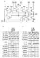
도 1의 (a)는 표시 장치의 일례를 도시하는 도면이고, 도 1의 (b)는 화소의 일례를 도시하는 회로도.
도 2의 (a)는 주사선 구동 회로의 구성 예를 도시하는 도면이고, 도 2의 (b)는 주사선 구동 회로의 동작 예를 도시하는 타이밍 차트이며, 도 2의 (c)는 펄스 출력 회로의 구성 예를 도시하는 도면.
도 3의 (a)는 펄스 출력 회로의 일례를 도시하는 회로도이고, 도 3의 (b) 및 (c)는 펄스 출력 회로의 동작의 일례를 각각 도시하는 타이밍 차트.
도 4는 컨트롤러의 구성 예를 도시하는 도면.
도 5는 트랜지스터의 일례를 도시하는 단면도.
도 6은 트랜지스터의 특성을 도시하는 도면.
도 7은 트랜지스터의 특성 평가용 소자의 회로도.
도 8은 트랜지스터의 특성 평가용 소자의 타이밍 차트.
도 9는 트랜지스터의 특성을 도시하는 도면.
도 10은 트랜지스터의 특성을 도시하는 도면.
도 11은 트랜지스터의 특성을 도시하는 도면.
도 12의 (a) 및 (b)는 펄스 출력 회로의 일례를 각각 도시하는 회로도.
도 13의 (a) 및 (b)는 펄스 출력 회로의 일례를 각각 도시하는 회로도.
도 14의 (a) 및 (b)는 펄스 출력 회로의 일례를 각각 도시하는 회로도.
도 15의 (a) 내지 (c)는 트랜지스터의 일례를 각각 도시하는 단면도.
도 16의 (a) 내지 (f)는 전자 기기의 일례를 각각 도시하는 도면.Fig. 1 (a) is a diagram showing an example of a display device, and Fig. 1 (b) is a circuit diagram showing an example of a pixel.
2B is a timing chart showing an example of the operation of the scanning line driving circuit, and FIG. 2C is a timing chart of the pulse output circuit of FIG. 2A. FIG. 2A is a diagram showing a configuration example of the scanning line driving circuit, Fig.
Fig. 3 (a) is a circuit diagram showing an example of a pulse output circuit, and Figs. 3 (b) and 3 (c) are timing charts each showing an example of the operation of a pulse output circuit.
4 is a diagram showing a configuration example of a controller.
5 is a cross-sectional view showing an example of a transistor.
6 is a diagram showing the characteristics of a transistor.
7 is a circuit diagram of a device for evaluating characteristics of a transistor.
8 is a timing chart of an element for evaluating characteristics of a transistor.
9 is a diagram showing the characteristics of a transistor.
10 is a diagram showing the characteristics of a transistor.
11 is a diagram showing the characteristics of a transistor.
12 (a) and 12 (b) are circuit diagrams each showing an example of a pulse output circuit.
13A and 13B are circuit diagrams each showing an example of a pulse output circuit.
14 (a) and 14 (b) are circuit diagrams each showing an example of a pulse output circuit.
15 (a) to 15 (c) are cross-sectional views each showing an example of a transistor.
Figs. 16A to 16F are views each showing an example of an electronic apparatus; Fig.
이하에서는, 본 발명의 실시 형태에 대해서 첨부 도면을 이용해서 상세하게 설명한다. 단, 본 발명은 이하의 설명에 한정되지 않고, 본 발명의 취지 및 그 범위를 벗어나지 않고도 그 형태 및 상세를 여러 가지로 변경할 수 있다는 것은, 당업자에게는 용이하게 이해된다는 점에 주목한다. 따라서, 본 발명은 이하에 도시하는 실시 형태의 기재 내용에 한정해서 해석되는 것은 아니다.Hereinafter, embodiments of the present invention will be described in detail with reference to the accompanying drawings. It should be noted, however, that the present invention is not limited to the following description, and it is easily understood by those skilled in the art that various changes in form and detail can be made without departing from the spirit and scope of the present invention. Therefore, the present invention is not construed as being limited to the description of the embodiments shown below.
(표시 장치의 예)(Example of display device)
본 발명의 한 실시예에 따른 표시 장치는 도 1의 (a) 및 (b), 도 2의 (a) 내지 (c), 도 3의 (a) 내지 (c), 도 4, 도 5, 도 6, 도 7, 도 8, 도 9, 도 10, 도 11, 도 12의 (a) 및 (b), 도 13의 (a) 및 (b), 도 14의 (a) 및 (b), 도 15의 (a) 내지 (c), 및 도 16의 (a) 내지 (f)와 관련하여 기술될 것이다.A display device according to an embodiment of the present invention is a display device having a plurality of display devices arranged in a matrix, (A) and 14 (b), Figs. 14 (a) and 14 (b) , Figures 15 (a) to (c), and Figures 16 (a) to (f).
도 1의 (a)는 표시 장치의 구성 예를 도시하는 도면이다. 도 1의 (a)에 도시하는 표시 장치는, 화소부(10), 주사선 구동 회로(11), 신호선 구동 회로(12), 컨트롤러(13), m개의 (m은 2 이상의 자연수)의 주사선(14), 및 n개의 (n은 2 이상의 자연수)의 신호선(15)을 포함한다. 주사선(14)은 서로 평행 또는 대략 평행하게 배치된다. 주사선(14)의 전위는 주사선 구동 회로(11)에 의해 제어된다. 신호선(15)은 서로 평행 또는 대략 평행하게 배치된다. 신호선(15)의 전위는 신호선 구동 회로(12)에 의해 제어된다. 화소부(10)는 매트릭스 형상(m행 n열)으로 배치된 복수의 화소(16)를 갖는다. 각각의 주사선(14)은 매트릭스 형상으로 배치된 복수의 화소(16) 중, 임의의 행에 배치된 화소(16)에 전기적으로 접속된다. 각각의 신호선(15)은 복수의 화소(16) 중, 임의의 열에 배치된 화소(16)에 전기적으로 접속된다. 주사선 구동 회로(11)에는, 컨트롤러(13)로부터 주사선 구동 회로용 개시 신호(GSP), 주사선 구동 회로용 클록 신호(GCK), 주사선 구동 회로용 부분 클록 신호(PGCK) 등의 신호, 및 고 전원 전위(Vdd)와 저 전원 전위(Vss) 등의 구동용 전원이 입력된다. 신호선 구동 회로(12)에는, 컨트롤러(13)로부터 신호선 구동 회로용 개시 신호(SP), 신호선 구동 회로용 클록 신호(SCK) 및 데이터 신호(DATA) 등의 신호, 및 고 전원 전위(Vdd)와 저 전원 전위(Vss) 등의 구동용 전원이 입력된다.1 (a) is a diagram showing a configuration example of a display device. The display device shown in Fig. 1 (a) includes a
도 1의 (b)는 도 1의 (a)에 도시된 표시 장치에 포함된 화소(16)의 회로도의 일례를 도시하는 도면이다. 도 1의 (b)에 도시된 화소(16)는 트랜지스터(17), 용량 소자(18) 및 액정 소자(19)를 포함한다. 트랜지스터(17)의 게이트는 주사선(14)에 전기적으로 접속된다. 트랜지스터(17)의 소스와 드레인 중 한쪽은 신호선(15)에 전기적으로 접속된다. 용량 소자(18)의 전극들 중 한쪽의 전극은 트랜지스터(17)의 소스와 드레인 중 다른 쪽에 전기적으로 접속된다. 용량 소자(18)의 전극들 중 다른쪽의 전극은 용량 소자 전위를 공급하는 배선(용량 소자선이라고도 함)에 전기적으로 접속된다. 액정 소자(19)의 전극들 중 한쪽의 전극(화소 전극이라고도 함)은 트랜지스터(17)의 소스와 드레인 중 다른 쪽 및 용량 소자(18)의 전극들 중 한쪽의 전극에 전기적으로 접속된다. 액정 소자(19)의 전극들 중 다른 쪽의 전극(대향 전극이라고도 함)은 대향 전위를 공급하는 배선에 전기적으로 접속된다. 트랜지스터(17)는 n 채널형의 트랜지스터이다. 용량 소자 전위와 대향 전위는 동일한 전위일 수 있다.1 (b) is a diagram showing an example of a circuit diagram of a
(주사선 구동 회로(11)의 구성 예)(Configuration example of scanning line drive circuit 11)
도 2의 (a)는 도 1의 (a)에 도시된 표시 장치에 포함된 주사선 구동 회로(11)의 구성 예를 도시하는 도면이다. 도 2의 (a)에 도시된 주사선 구동 회로(11)는, 주사선 구동 회로용의 제1 내지 제4 클록 신호(GCK1 내지 GCK4)(이후, "제1 클록 신호(GCK1)" 내지 "제4 클록 신호(GCK4)"라고 함)를 각각 공급하는 배선, 주사선 구동 회로용의 제1 내지 제4 부분 클록 신호(PGCK1 내지 PGCK4)(이후, "제1 부분 클록 신호(PGCK1)" 내지 "제4 부분 클록 신호(PGCK4)"라고 함)을 각각 공급하는 배선, 및 제1 내지 제m 행에 배치된 각각의 주사선(14)에 전기적으로 접속된 제1 내지 제m 펄스 출력 회로(20_1 내지 20_m)를 포함한다.2 (a) is a diagram showing a configuration example of the scanning
도 2의 (b)는, 상기 신호의 구체적인 파형의 예를 도시하는 도면이다. 도 2의 (b)에 도시된 제1 클록 신호(GCK1)는, 하이 레벨의 전위(도 2의 (b)에서 고 전원 전위(Vdd)와 등전위) 및 로우 레벨의 전위(도 2의 (b)에서 저 전원 전위(Vss)와 등전위)을 주기적으로 반복하고, 듀티비(duty ratio)가 1/2이다. 제2 클록 신호(GCK2)는, 제1 클록 신호(GCK1)로부터 1/4 사이클만큼 시프트된다. 제3 클록 신호(GCK3)은, 제1 클록 신호(GCK1)로부터 1/2 사이클만큼 시프트된다(즉, GCK3은 제1 클록 신호(GCK1)의 반전 신호이다). 제4 클록 신호(GCK4)는, 제1 클록 신호(GCK1)로부터 3/4 사이클만큼 시프트된다(즉, GCK4는 제2 클록 신호(GCK2)의 반전 신호이다). 제1 부분 클록 신호(PGCK1)은, 제1 클록 신호(GCK1) 및 고정 전위(도 2의 (b)에서 저 전원 전위(Vss)와 등전위) 중 어느 하나를 선택적으로 나타낸다. 제1 부분 클록 신호(PGCK1)가 GCK1과 고정 전위 중 어느 쪽을 나타낼지는 컨트롤러(13)에 의해 제어된다. 마찬가지로, 제2 부분 클록 신호(PGCK2)은, 제2 클록 신호(GCK2) 및 고정 전위 중 어느 하나를 선택적으로 나타낸다. 제3 부분 클록 신호(PGCK3)는, 제3 클록 신호(GCK3) 및 고정 전위 중 어느 하나를 선택적으로 나타낸다. 제4 부분 클록 신호(PGCK4)는, 제4 클록 신호(GCK4) 및 고정 전위 중 어느 하나를 선택적으로 나타낸다.2 (b) is a diagram showing an example of a specific waveform of the signal. The first clock signal GCK1 shown in FIG. 2B has a high level potential (equal to the high power source potential Vdd in FIG. 2 (b)) and a low level potential (Vss) and the equipotential) are periodically repeated, and the duty ratio is 1/2. The second clock signal GCK2 is shifted by 1/4 cycle from the first clock signal GCK1. The third clock signal GCK3 is shifted by 1/2 cycle from the first clock signal GCK1 (that is, GCK3 is an inverted signal of the first clock signal GCK1). The fourth clock signal GCK4 is shifted by 3/4 cycle from the first clock signal GCK1 (that is, GCK4 is the inverted signal of the second clock signal GCK2). The first partial clock signal PGCK1 selectively indicates either the first clock signal GCK1 or the fixed potential (equal to the low power source potential Vss in FIG. 2 (b)). It is controlled by the
상술한 표시 장치에서는, 동일한 구성을 갖는 회로가 제1 내지 제m 펄스 출력 회로(20_1 내지 20_m)로서 사용될 수 있다. 펄스 출력 회로에 포함된 복수의 단자들의 전기적인 접속 관계는 펄스 출력 회로마다 상이하다는 점에 주목한다. 구체적인 접속 관계에 대해서는 도 2의 (a) 및 (c)를 참조하여 설명한다.In the above-described display device, a circuit having the same configuration can be used as the first to m-th pulse output circuits 20_1 to 20_m. Note that the electrical connection relationship of the plurality of terminals included in the pulse output circuit is different for each pulse output circuit. The concrete connection relationship will be described with reference to Figs. 2A and 2C.
제1 내지 제m 펄스 출력 회로(20_1 내지 20_m) 각각은 단자(21 내지 28)를 갖는다. 단자(21 내지 25) 및 단자(27)는 입력 단자이다. 단자(26 및 28)는 출력 단자이다.Each of the first to m-th pulse output circuits 20_1 to 20_m has
우선, 단자(21)에 대해서 서술한다. 제1 펄스 출력 회로(20_1)의 단자(21)는, 주사선 구동 회로용 개시 신호(GSP)를 공급하는 배선에 전기적으로 접속된다. 제2 내지 제m 펄스 출력 회로(20_2 내지 20_m)의 각각의 단자(21)는 전단의 펄스 출력 회로의 단자(28)에 전기적으로 접속된다.First, the terminal 21 will be described. The terminal 21 of the first pulse output circuit 20_1 is electrically connected to the wiring for supplying the scanning line driving circuit start signal GSP. Each of the
다음, 단자(22)에 대해서 서술한다. 제(4a+1)의 펄스 출력 회로(a=0, 1, 2 내지 (m-4)/4)의 단자(22)는, 제1 클록 신호(GCK1)를 공급하는 배선에 전기적으로 접속된다. 제(4a+2)의 펄스 출력 회로의 단자(22)는, 제2 클록 신호(GCK2)를 공급하는 배선에 전기적으로 접속된다. 제(4a+3)의 펄스 출력 회로의 단자(22)는, 제3 클록 신호(GCK3)를 공급하는 배선에 전기적으로 접속된다. 제(4a+4)의 펄스 출력 회로의 단자(22)는, 제4 클록 신호(GCK4)를 공급하는 배선에 전기적으로 접속된다.Next, the terminal 22 will be described. The terminal 22 of the pulse output circuit (a = 0, 1, 2 to (m-4) / 4) of the (4a + 1) th stage is electrically connected to the wiring for supplying the first clock signal GCK1 . The terminal 22 of the pulse output circuit of (4a + 2) is electrically connected to the wiring for supplying the second clock signal GCK2. The terminal 22 of the pulse output circuit of (4a + 3) is electrically connected to the wiring for supplying the third clock signal GCK3. The terminal 22 of the pulse output circuit of (4a + 4) is electrically connected to the wiring for supplying the fourth clock signal GCK4.
이어서, 단자(23)에 대해서 서술한다. 제(4a+1)의 펄스 출력 회로의 단자(23)는, 제2 클록 신호(GCK2)를 공급하는 배선에 전기적으로 접속된다. 제(4a+2)의 펄스 출력 회로의 단자(23)는, 제3 클록 신호(GCK3)를 공급하는 배선에 전기적으로 접속된다. 제(4a+3)의 펄스 출력 회로의 단자(23)는, 제4 클록 신호(GCK4)를 공급하는 배선에 전기적으로 접속된다. 제(4a+4)의 펄스 출력 회로의 단자(23)는, 제1 클록 신호(GCK1)를 공급하는 배선에 전기적으로 접속된다.Next, the terminal 23 will be described. The terminal 23 of the pulse output circuit of (4a + 1) is electrically connected to the wiring for supplying the second clock signal GCK2. The terminal 23 of the pulse output circuit of (4a + 2) is electrically connected to the wiring for supplying the third clock signal GCK3. The terminal 23 of the pulse output circuit of (4a + 3) is electrically connected to the wiring for supplying the fourth clock signal GCK4. The terminal 23 of the pulse output circuit of (4a + 4) is electrically connected to the wiring for supplying the first clock signal GCK1.
이어서, 단자(24)에 대해서 서술한다. 제(4a+1)의 펄스 출력 회로의 단자(24)는, 제3 클록 신호(GCK3)를 공급하는 배선에 전기적으로 접속된다. 제(4a+2)의 펄스 출력 회로의 단자(24)는, 제4 클록 신호(GCK4)를 공급하는 배선에 전기적으로 접속된다. 제(4a+3)의 펄스 출력 회로의 단자(24)는, 제1 클록 신호(GCK1)를 공급하는 배선에 전기적으로 접속된다. 제(4a+4)의 펄스 출력 회로의 단자(24)는, 제2 클록 신호(GCK2)를 공급하는 배선에 전기적으로 접속된다.Next, the terminal 24 will be described. The terminal 24 of the pulse output circuit of (4a + 1) is electrically connected to the wiring for supplying the third clock signal GCK3. The terminal 24 of the pulse output circuit of (4a + 2) is electrically connected to the wiring for supplying the fourth clock signal GCK4. The terminal 24 of the pulse output circuit of (4a + 3) is electrically connected to the wiring for supplying the first clock signal GCK1. The terminal 24 of the pulse output circuit of (4a + 4) is electrically connected to the wiring for supplying the second clock signal GCK2.
이어서, 단자(25)에 대해서 서술한다. 제(4a+1)의 펄스 출력 회로의 단자(25)는, 제1 부분 클록 신호(PGCK1)를 공급하는 배선에 전기적으로 접속된다. 제(4a+2)의 펄스 출력 회로의 단자(25)는, 제2 부분 클록 신호(PGCK2)를 공급하는 배선에 전기적으로 접속된다. 제(4a+3)의 펄스 출력 회로의 단자(25)는, 제3 부분 클록 신호(PGCK3)를 공급하는 배선에 전기적으로 접속된다. 제(4a+4)의 펄스 출력 회로의 단자(25)는, 제4 부분 클록 신호(PGCK4)를 공급하는 배선에 전기적으로 접속된다.Next, the terminal 25 will be described. The terminal 25 of the pulse output circuit of (4a + 1) is electrically connected to the wiring for supplying the first partial clock signal PGCK1. The terminal 25 of the pulse output circuit of (4a + 2) is electrically connected to the wiring for supplying the second partial clock signal PGCK2. The terminal 25 of the pulse output circuit of (4a + 3) is electrically connected to the wiring for supplying the third partial clock signal PGCK3. The terminal 25 of the pulse output circuit of (4a + 4) is electrically connected to the wiring for supplying the fourth partial clock signal PGCK4.
이어서, 단자(26)에 대해서 서술한다. 제x 펄스 출력 회로(x는, 1 이상 m 이하의 자연수)의 단자(26)는, x행에 배치된 주사선(14)에 전기적으로 접속된다.Next, the terminal 26 will be described. The
이어서, 단자(27)에 대해서 서술한다. 제b 펄스 출력 회로(b는, 1 이상 m-2 이하의 자연수)의 단자(27)는, 제(b+2) 펄스 출력 회로의 단자(28)에 전기적으로 접속된다. 제(m-1) 펄스 출력 회로의 단자(27)는, 제1 주사선 구동 회로용 스톱 신호(GSTP1)를 공급하는 배선에 전기적으로 접속된다. 제m 펄스 출력 회로의 단자(27)는, 제2 주사선 구동 회로용 스톱 신호(GSTP2)를 공급하는 배선에 전기적으로 접속된다. 제(m+1) 펄스 출력 회로가 제공된다면, 제1 주사선 구동 회로용 스톱 신호(GSTP1)는, 제(m+1) 펄스 출력 회로의 단자(28)로부터 출력되는 신호에 상당한다. 마찬가지로, 제(m+2) 펄스 출력 회로가 제공되면, 제2 주사선 구동 회로용 스톱 신호(GSTP2)는, 제(m+2) 펄스 출력 회로의 단자(28)로부터 출력되는 신호에 상당한다. 구체적으로는, 이들 신호는, 예를 들어, 더미(dummy) 회로로서 제(m+1) 펄스 출력 회로 및 제(m+2) 펄스 출력 회로가 실제로 제공되거나, 컨트롤러(13)로부터 신호가 직접 출력될 때, 주사선 구동 회로(11)에 공급될 수 있다.Next, the terminal 27 will be described. The terminal 27 of the b-th pulse output circuit (b is a natural number equal to or larger than 1 and equal to or smaller than m-2) is electrically connected to the
각 펄스 출력 회로의 단자(28)의 접속 관계는 상기에서 설명되었고; 따라서 여기에서는 전술의 설명을 적용한다.The connection relationship of the
(펄스 출력 회로의 구성 예)(Configuration Example of Pulse Output Circuit)
도 3의 (a)는, 도 2의 (a) 및 (c)에 도시된 펄스 출력 회로의 구성 예를 도시하는 도면이다. 도 3의 (a)에 도시된 펄스 출력 회로는 트랜지스터(31 내지 41)를 포함한다.Fig. 3 (a) is a diagram showing a configuration example of the pulse output circuit shown in Figs. 2 (a) and 2 (c). The pulse output circuit shown in FIG. 3 (a) includes
트랜지스터(31)의 소스와 드레인 중 한쪽은 고 전원 전위(Vdd)를 공급하는 배선(이하, 고 전원 전위선이라고도 함)에 전기적으로 접속된다. 트랜지스터(31)의 게이트는 단자(21)에 전기적으로 접속된다.One of the source and the drain of the
트랜지스터(32)의 소스와 드레인 중 한쪽은 저 전원 전위(Vss)를 공급하는 배선(이하, 저 전원 전위선이라고도 함)에 전기적으로 접속된다. 트랜지스터(32)의 소스와 드레인 중 다른 쪽은 트랜지스터(31)의 소스와 드레인 중 다른 쪽에 전기적으로 접속된다.One of the source and the drain of the
트랜지스터(33)의 소스와 드레인 중 한쪽은 단자(22)에 전기적으로 접속된다. 트랜지스터(33)의 소스와 드레인 중 다른 쪽은 단자(28)에 전기적으로 접속된다.One of the source and the drain of the
트랜지스터(34)의 소스와 드레인 중 한쪽은 저 전원 전위선에 전기적으로 접속된다. 트랜지스터(34)의 소스와 드레인 중 다른 쪽은 단자(28)에 전기적으로 접속된다. 트랜지스터(34)의 게이트는 트랜지스터(32)의 게이트에 전기적으로 접속된다.One of the source and the drain of the
트랜지스터(35)의 소스와 드레인 중 한쪽은 저 전원 전위선에 전기적으로 접속된다. 트랜지스터(35)의 소스와 드레인 중 다른 쪽은 트랜지스터(32)의 게이트 및 트랜지스터(34)의 게이트에 전기적으로 접속된다. 트랜지스터(35)의 게이트는 단자(21)에 전기적으로 접속된다.One of the source and the drain of the
트랜지스터(36)의 소스와 드레인 중 한쪽은 고 전원 전위선에 전기적으로 접속된다. 트랜지스터(36)의 소스와 드레인 중 다른 쪽은 트랜지스터(32)의 게이트, 트랜지스터(34)의 게이트, 및 트랜지스터(35)의 소스와 드레인 중 다른 쪽에 전기적으로 접속된다. 트랜지스터(36)의 게이트는 단자(27)에 전기적으로 접속된다. 트랜지스터(36)의 소스와 드레인 중 한쪽이, 저 전원 전위(Vss)보다 고전위이며 고 전원 전위(Vdd)보다 저전위인 전원 전위(Vcc)를 공급하는 배선에 전기적으로 접속되는 구성을 채택할 수 있다는 점에 주목한다.One of the source and the drain of the
트랜지스터(37)의 소스와 드레인 중 한쪽은 고 전원 전위선에 전기적으로 접속된다. 트랜지스터(37)의 게이트는 단자(24)에 전기적으로 접속된다. 트랜지스터(37)의 소스와 드레인 중 한쪽이, 전원 전위(Vcc)를 공급하는 배선에 전기적으로 접속되는 구성을 채택할 수 있다는 점에 주목한다.One of the source and the drain of the
트랜지스터(38)의 소스와 드레인 중 한쪽이 트랜지스터(32)의 게이트, 트랜지스터(34)의 게이트, 트랜지스터(35)의 소스와 드레인 중 다른 쪽, 및 트랜지스터(36)의 소스와 드레인 중 다른 쪽에 전기적으로 접속된다. 트랜지스터(38)의 소스와 드레인 중 다른 쪽이 트랜지스터(37)의 소스와 드레인 중 다른 쪽에 전기적으로 접속된다. 트랜지스터(38)의 게이트는 단자(23)에 전기적으로 접속된다.One of the source and the drain of the
트랜지스터(39)의 소스와 드레인 중 한쪽은 트랜지스터(31)의 소스와 드레인 중 다른 쪽 및 트랜지스터(32)의 소스와 드레인 중 다른 쪽에 전기적으로 접속된다. 트랜지스터(39)의 소스와 드레인 중 다른 쪽은 트랜지스터(33)의 게이트에 전기적으로 접속된다. 트랜지스터(39)의 게이트는 고 전원 전위선에 전기적으로 접속된다.One of the source and the drain of the
트랜지스터(40)의 소스와 드레인 중 한쪽은 단자(25)에 전기적으로 접속된다. 트랜지스터(40)의 소스와 드레인 중 다른 쪽은 단자(26)에 전기적으로 접속된다. 트랜지스터(40)의 게이트는 트랜지스터(33)의 게이트 및 트랜지스터(39)의 소스와 드레인 중 다른 쪽에 전기적으로 접속된다.One of the source and the drain of the
트랜지스터(41)의 소스와 드레인 중 한쪽은 저 전원 전위선에 전기적으로 접속되다. 트랜지스터(41)의 소스와 드레인 중 다른 쪽은 단자(26)에 전기적으로 접속된다. 트랜지스터(41)의 게이트는 트랜지스터(32)의 게이트, 트랜지스터(34)의 게이트, 트랜지스터(35)의 소스와 드레인 중 다른 쪽, 트랜지스터(36)의 소스와 드레인 중 다른 쪽, 및 트랜지스터(38)의 소스와 드레인 중 한쪽에 전기적으로 접속된다.One of the source and the drain of the
이하의 설명에서, 트랜지스터(33)의 게이트, 트랜지스터(39)의 소스와 드레인 중 다른 쪽, 및 트랜지스터(40)의 게이트가 전기적으로 서로 접속하는 노드를 노드 A로 한다는 점에 주목한다. 또한, 트랜지스터(32)의 게이트, 트랜지스터(34)의 게이트, 트랜지스터(35)의 소스와 드레인 중 다른 쪽, 트랜지스터(36)의 소스와 드레인 중 다른 쪽, 트랜지스터(38)의 소스와 드레인 중 한쪽, 및 트랜지스터(41)의 게이트가 전기적으로 서로 접속하는 노드를 노드 B로 한다는 점에 주목한다.In the following description, it is noted that the node A is a node where the gate of the
(펄스 출력 회로의 동작 예)(Operation example of pulse output circuit)
상술한 펄스 출력 회로의 동작 예에 대해서 도 3의 (b) 및 (c)를 참조하여 설명한다. 또한, 도 3의 (b)는, 펄스 출력 회로의 단자(25)에 입력되는, 제1 내지 제4 부분 클록 신호(PGCK1 내지 PGCK4) 중 하나가 제1 내지 제4 클록 신호(GCK1 내지 GCK4) 중 하나인 경우에 펄스 출력 회로의 각 단자에 입력된 신호의 전위, 및 노드 A 및 노드 B의 전위를 도시한다. 도 3의 (c)는, 펄스 출력 회로의 단자(25)에 입력되는, 제1 내지 제4 부분 클록 신호(PGCK1 내지 PGCK4) 중 하나가 고정 전위(저 전원 전위 Vss)인 경우에 펄스 출력 회로의 각 단자에 입력된 신호의 전위, 및 노드 A 및 노드 B의 전위를 도시하고 있다. 또한, 도 3의 (b) 및 (c)에서는, 각각의 조건에서, 제1 펄스 출력 회로(20_1)의 각 단자에 입력되는 신호가 괄호로 도시된다. 도 3의 (b) 및 (c)에서, 제1 펄스 출력 회로(20_1)의 단자(26)의 출력 신호(Gout1) 및 단자(28)의 출력 신호(SRout1) 또한 도시된다. 또한, 도 3의 (b) 및 (c)는 제2 펄스 출력 회로(20_2)의 단자(26)의 출력 신호(Gout2) 및 단자(28)의 출력 신호(SRout2), 및 제3 펄스 출력 회로(20_3)의 단자(26)의 출력 신호(Gout3) 및 단자(28)의 출력 신호(SRout3)(SRout3은 제1 펄스 출력 회로(20_1)의 단자(27)의 입력 신호에 상당함)를 도시한다. 또한, 도 3의 (b) 및 (c)에서, Gout는 펄스 출력 회로로부터 주사선으로의 출력 신호를 나타내고, SRout는 펄스 출력 회로로부터 후단의 펄스 출력 회로로의 출력 신호를 나타낸다는 점에 주목한다.An operation example of the above-described pulse output circuit will be described with reference to Figs. 3 (b) and 3 (c). 3B shows that one of the first to fourth partial clock signals PGCK1 to PGCK4 input to the
우선, 도 3의 (b)를 참조하여, 펄스 출력 회로의 단자(25)에 입력되는, 제1 내지 제4 부분 클록 신호(PGCK1 내지 PGCK4) 중 하나가 제1 내지 제4 클록 신호(GCK1 내지 GCK4) 중 하나인 경우에 대해서 설명한다.3 (b), one of the first to fourth partial clock signals PGCK1 to PGCK4 input to the
기간 t1에서, 펄스 출력 회로의 단자(21)에는 고 전원 전위(Vdd)가 입력된다. 따라서, 트랜지스터(31 및 35)가 온 상태로 된다. 그 결과, 노드 A의 전위가 하이 레벨의 전위(고 전원 전위(Vdd)로부터 트랜지스터(31) 또는 트랜지스터(39)의 임계 전압만큼 강하된 전위)로 상승하고, 노드 B의 전위가 저 전원 전위(Vss)로 강하한다. 이에 따라, 트랜지스터(33 및 40)가 온 상태로 되고, 트랜지스터(32, 34 및 41)가 오프 상태로 된다. 따라서, 기간 t1에서, 펄스 출력 회로의 단자(28)로부터 출력되는 신호는 단자(22)에 입력되는 신호가 되고, 단자(26)로부터 출력되는 신호는 단자(25)에 입력되는 신호가 된다. 여기서, 기간 t1에서, 펄스 출력 회로의 단자(22) 및 단자(25)에 입력되는 신호들은 둘 다 저 전원 전위(Vss)이다. 따라서, 기간 t1에서, 펄스 출력 회로는, 후단의 펄스 출력 회로의 단자(21), 및 단자(26)에 전기적으로 접속된 주사선에 저 전원 전위(Vss)를 출력한다. 또한, 기간 t1에서의 펄스 출력 회로의 출력 신호와는 직접 관여되지는 않지만, 단자(23)에 저 전원 전위(Vss)가 입력되기 때문에 트랜지스터(38)가 오프 상태로 되고; 단자(24)에 고 전원 전위(Vdd)가 입력되기 때문에 트랜지스터(37)가 온 상태로 되며; 단자(27)에 저 전원 전위(Vss)가 입력되기 때문에 트랜지스터(36)가 오프 상태로 된다는 점에 주목한다.In the period t1, the high power supply potential Vdd is input to the
기간 t2에서, 펄스 출력 회로의 단자(22 및 25)에 고 전원 전위(Vdd)가 입력된다. 노드 A의 전위(트랜지스터(39)의 소스의 전위)는, 기간 t1에서 하이 레벨의 전위까지 상승하여, 트랜지스터(39)가 오프 상태로 된다는 점에 주목한다. 이때, 단자(22 및 25)에 고 전원 전위(Vdd)를 입력함으로써, 트랜지스터(33)의 소스와 게이트 및 트랜지스터(40)의 소스와 게이트의 용량 결합에 의해, 노드 A의 전위(트랜지스터(33)의 게이트 및 트랜지스터(40)의 게이트의 전위)가 더욱 상승한다(부트스트랩 동작). 또한, 부트스트랩 동작을 행함으로써, 단자(28 및 26)로부터 출력되는 전위를, 저하시키지 않고도, 고 전원 전위(Vdd)로 설정할 수 있다. 따라서, 기간 t2에서, 펄스 출력 회로는, 후단의 펄스 출력 회로의 단자(21), 및 단자(26)에 전기적으로 접속된 주사선에 고 전원 전위(Vdd)를 출력한다. 기간 t2에서의 펄스 출력 회로의 출력 신호에는 직접 관여되지 않지만, 단자(24)에 저 전원 전위(Vss)가 입력되기 때문에 트랜지스터(37)는 오프 상태로 된다는 점에 주목한다.In the period t2, the high power supply potential Vdd is input to the
기간 t3에서, 펄스 출력 회로의 단자(21)에 저 전원 전위(Vss)가 입력된다. 이에 의해, 트랜지스터(31 및 35)가 오프 상태로 된다. 이때, 노드 A는 부유 상태(floating state)를 유지하게 되어, 트랜지스터(33 및 40)가 온 상태를 유지한다. 따라서, 기간 t3에서, 펄스 출력 회로의 단자(28)로부터 출력되는 신호는 단자(22)에 입력되는 신호가 되고, 단자(26)로부터 출력되는 신호는 단자(25)에 입력되는 신호가 된다. 여기서, 기간 t3에서, 펄스 출력 회로의 단자(22 및 25) 둘 다에는 고 전원 전위(Vdd)가 입력된다. 따라서, 기간 t3에서, 펄스 출력 회로는, 후단의 펄스 출력 회로의 단자(21), 및 단자(26)에 전기적으로 접속된 주사선에 고 전원 전위(Vdd)를 출력한다. 기간 t3에서의 펄스 출력 회로의 출력 신호에는 직접 관여되지 않지만, 단자(23)에 고 전원 전위(Vdd)가 입력되기 때문에 트랜지스터(38)가 온 상태로 된다는 점에 주목한다.In the period t3, the low power supply potential Vss is input to the
기간 t4에서, 펄스 출력 회로의 단자(24 및 27)에 고 전원 전위(Vdd)가 입력된다. 따라서, 트랜지스터(36 및 37)가 온 상태로 된다. 그 결과, 노드 B의 전위가 하이 레벨의 전위(트랜지스터(36), 트랜지스터(37) 또는 트랜지스터(38)의 임계 전압만큼 고 전원 전위(Vdd)로부터 강하된 전위)로 상승한다. 이에 따라, 트랜지스터(32, 34 및 41)가 온 상태로 된다. 또한, 트랜지스터(32)가 온 상태로 되면, 트랜지스터(39)의 소스(소스와 드레인 중 한쪽)의 전위가 저 전원 전위(Vss)가 된다. 따라서, 트랜지스터(39)가 온 상태로 되어, 노드 A의 전위가 저 전원 전위(Vss)로 강하한다. 이에 따라, 트랜지스터(33 및 40)가 오프 상태로 된다. 따라서, 기간 t4에서, 펄스 출력 회로의 단자(28)로부터 출력되는 신호 및 단자(26)로부터 출력되는 신호는 저 전원 전위(Vss)이다. 즉, 기간 t4에서, 펄스 출력 회로는, 후단의 펄스 출력 회로의 단자(21), 및 단자(26)에 전기적으로 접속된 주사선에 저 전원 전위(Vss)를 출력한다.In the period t4, the high power supply potential Vdd is input to the
기간 t5 또는 그 이후에서, 펄스 출력 회로의 단자(21)에 고 전원 전위(Vdd)가 입력될 때까지, 노드 A는 저 전원 전위(Vss)를 유지하고, 노드 B는 하이 레벨의 전위를 유지한다. 따라서, 해당 기간에서, 해당 펄스 출력 회로는, 후단의 펄스 출력 회로의 단자(21), 및 단자(26)에 전기적으로 접속된 주사선에 저 전원 전위(Vss)를 출력한다.The node A maintains the low power supply potential Vss until the high power supply potential Vdd is input to the
다음에, 도 3의 (c)를 참조하여, 펄스 출력 회로의 단자(25)에 입력되는, 제1 내지 제4 부분 클록 신호(PGCK1 내지 PGCK4) 중 하나가 고정 전위(저 전원 전위 Vss)인 경우에 대해서 설명한다.Next, referring to FIG. 3C, it is assumed that one of the first to fourth partial clock signals PGCK1 to PGCK4 input to the
기간 t1에서, 펄스 출력 회로의 단자(21)에 고 전원 전위(Vdd)가 입력된다. 상술한 바와 같이, 기간 t1에서, 펄스 출력 회로의 단자(28)로부터 출력되는 신호는 단자(22)에 입력되는 신호가 되고, 단자(26)로부터 출력되는 신호는 단자(25)에 입력되는 신호가 된다. 여기서, 기간 t1에서, 펄스 출력 회로의 단자(22)에 입력되는 신호 및 단자(25)에 입력되는 신호 둘 다는 저 전원 전위(Vss)이다. 따라서, 기간 t1에서, 펄스 출력 회로는, 후단의 펄스 출력 회로의 단자(21), 및 단자(26)에 전기적으로 접속된 주사선에 저 전원 전위(Vss)를 출력한다.In the period t1, the high power supply potential Vdd is input to the
기간 t2에서, 펄스 출력 회로의 단자(22)에 고 전원 전위(Vdd)가 입력된다. 상술한 바와 같이, 부트스트랩 동작을 행함으로써, 단자(28)로부터 출력되는 전위는, 저하되지 않고, 고 전원 전위(Vdd)로 설정될 수 있다. 상술한 설명과는 달리, 단자(25)에 입력되는 신호는 저 전원 전위(Vss)로부터 변화되지 않고 유지된다는 점에 주목한다. 따라서, 펄스 출력 회로의 단자(26)로부터 출력되는 신호는 저 전원 전위(Vss)로부터 변화되지 않은 채로 남아 있다.In the period t2, the high power supply potential Vdd is input to the
기간 t3에서, 펄스 출력 회로의 단자(21)에 저 전원 전위(Vss)가 입력된다. 상술한 바와 같이, 기간 t3에서, 펄스 출력 회로의 단자(28)로부터 출력되는 신호는 단자(22)에 입력되는 신호가 되고, 단자(26)로부터 출력되는 신호는 단자(25)에 입력되는 신호가 된다. 여기서, 기간 t3에서, 펄스 출력 회로의 단자(22)에는 고 전원 전위(Vdd)가 입력되고, 단자(25)에는 저 전원 전위(Vss)가 입력된다. 따라서, 기간 t3에서, 펄스 출력 회로는, 후단의 펄스 출력 회로의 단자(21)에 고 전원 전위(Vdd)를 출력하고, 단자(26)에 전기적으로 접속된 주사선에 저 전원 전위(Vss)를 출력한다.In the period t3, the low power supply potential Vss is input to the
기간 t4에서, 펄스 출력 회로의 단자(24 및 27)에 고 전원 전위(Vdd)가 입력된다. 상술한 바와 같이, 기간 t4에서, 펄스 출력 회로의 단자(28)로부터 출력되는 신호 및 단자(26)로부터 출력되는 신호는 저 전원 전위(Vss)이다. 따라서, 기간 t4에서, 펄스 출력 회로는, 후단의 펄스 출력 회로의 단자(21), 및 단자(26)에 전기적으로 접속된 주사선에 저 전원 전위(Vss)를 출력한다.In the period t4, the high power supply potential Vdd is input to the
기간 t5 또는 그 이후에서, 펄스 출력 회로의 단자(21)에 고 전원 전위(Vdd)가 입력될 때까지, 노드 A가 저 전원 전위(Vss)를 유지하고, 노드 B가 하이 레벨의 전위를 유지한다. 따라서, 해당 기간에서, 펄스 출력 회로는 후단의 펄스 출력 회로의 단자(21), 및 단자(26)에 전기적으로 접속된 주사선에 저 전원 전위(Vss)를 출력한다.The node A maintains the low power supply potential Vss until the high power supply potential Vdd is input to the
(펄스 출력 회로 및 이를 포함하는 주사선 구동 회로)(Pulse output circuit and scanning line driving circuit including the same)
상술한 펄스 출력 회로에서는, 기간 t2 및 기간 t3에서 주사선에 선택 신호(고 전원 전위(Vdd))가 출력되는 지의 여부가 단자(25)에 입력되는 신호에 따라 선택된다. 구체적으로는, 펄스 출력 회로는, 단자(25)에 입력되는 신호가 제1 주사선 구동 회로용 클록 신호인 경우에는 선택 신호를 출력하고, 단자(25)에 입력되는 신호가 고정 전위(저 전원 전위(Vss))인 경우에는 비선택 신호를 출력한다. 또한, 펄스 출력 회로는, 상기의 동작과는 무관하게, 선택 신호를 후단의 펄스 출력 회로로 시프트하는 기능도 갖는다. 즉, 시프트 레지스터는 복수의 펄스 출력 회로를 이용하여 형성될 수 있다.In the above-described pulse output circuit, whether or not the selection signal (high power supply potential Vdd) is outputted to the scanning line in the period t2 and the period t3 is selected according to the signal inputted to the terminal 25. [ Specifically, the pulse output circuit outputs a selection signal when the signal input to the terminal 25 is the clock signal for the first scanning line driving circuit, and outputs a selection signal when the signal input to the terminal 25 has a fixed potential (Vss)), it outputs a non-selection signal. The pulse output circuit also has a function of shifting the selection signal to the pulse output circuit in the subsequent stage regardless of the above operation. That is, the shift register can be formed using a plurality of pulse output circuits.
본 명세서에서 개시된 표시 장치에서는, 주사선 구동 회로가 해당 시프트 레지스터를 갖는다. 따라서, 표시 장치에서, 선택 신호의 공급은 주사선마다 제어하는 것이 가능하다. 즉, 본 명세서에서 개시되는 표시 장치에서는, 임의의 영역에만 화상의 재기입을 행하는 것이 가능하다.In the display device disclosed in this specification, the scanning line driving circuit has a corresponding shift register. Therefore, in the display device, the supply of the selection signal can be controlled for each scanning line. That is, in the display device disclosed in this specification, it is possible to rewrite the image only in an arbitrary area.
또한, 본 명세서에서 개시되는 표시 장치는, 상기의 동작을, 제1 내지 제4 클록 신호(GCK1 내지 GCK4) 또는 고정 전위(저 전원 전위(Vss))를 각각 나타내는 신호를 공급하는 배선을 제공함으로써 실현 가능하다. 따라서, 본 명세서에서 개시되는 표시 장치에서는, 부분 구동이 가능하면서 배선을 포함하는 회로의 구성이 간략화될 수 있다.Further, the display device disclosed in this specification can perform the above-described operation by providing a wiring for supplying a signal indicating the first to fourth clock signals (GCK1 to GCK4) or the fixed potential (low power supply potential (Vss)), respectively It is feasible. Therefore, in the display device disclosed in this specification, the structure of the circuit including the wiring, which can be partially driven, can be simplified.
배선에 클록 신호 및 고정 전위 중 어느 것을 공급할지는, 컨트롤러(13)에 의해 제어된다. 이하에서, 컨트롤러(13)의 구체적인 구성 및 배선에 대하여 출력하는 신호의 선택 방법의 일례에 대해서 도시한다.The
(컨트롤러(13)의 구성 예)(Configuration example of the controller 13)
도 4는, 통상 모드, 부분 구동 모드 및 대기 모드인 3개의 모드를 갖는 컨트롤러(13)의 구성 예를 도시한다. 통상 모드에서는, 제1 내지 제4 부분 클록 신호(PGCK1 내지 PGCK4)가 기간에 상관없이, 제1 내지 제4 클록 신호(GCK1 내지 GCK4)와 동일하다는 점에 주목한다. 부분 구동 모드에서는, 제1 내지 제4 부분 클록 신호(PGCK1 내지 PGCK4)가 제1 내지 제4 클록 신호(GCK1 내지 GCK4) 또는 고정 전위와 동일하다. 대기 모드에서는, 주사선 구동 회로(11) 및 신호선 구동 회로(12)에 클록 신호 등이 공급되지 않는다. 도 4에 도시된 컨트롤러(13)는 신호 생성 회로(131), 기억 회로(132), 비교 회로(133), 선택 회로(134) 및 표시 제어 회로(135)를 포함한다.Fig. 4 shows a configuration example of the
신호 생성 회로(131)는 주사선 구동 회로(11) 및 신호선 구동 회로(12)를 동작시키기 위한 신호 및 화소부(10)에 화상을 형성하기 위한 신호를 생성한다. 구체적으로, 신호 생성 회로(131)는 화소부(10)에 매트릭스 형상으로 배치된 복수의 화소에 입력되는 화상 신호(Data), 주사선 구동 회로(11) 또는 신호선 구동 회로(12)의 동작을 제어하는 신호(예를 들어, 개시 신호(SP) 및 클록 신호(CK)), 및 전원 전압인 고 전원 전위(Vdd)와 저 전원 전위(Vss) 등을 생성 및 출력한다. 도 4에 도시된 컨트롤러(13)에서, 신호 생성 회로(131)는 기억 회로(132)에 화상 신호(Data)를 출력하고, 표시 제어 회로(135)에 주사선 구동 회로(11) 또는 신호선 구동 회로(12)의 동작을 제어하는 신호를 출력한다는 점에 주목한다. 신호 생성 회로(131)로부터 기억 회로(132)에 출력되는 화상 신호(Data)가 아날로그 신호일 경우에는, A/D 컨버터 등을 통하여, 화상 신호(Data)를 디지털 신호로 변환할 수도 있다.The
기억 회로(132)는 화소부(10)에서, 제1 내지 제n 화상(n은 자연수)을 형성하기 위한 화상 신호를 기억하는 복수의 메모리(136)를 포함한다. 메모리(136)는 동적 랜덤 액세스 메모리(dynamic random access memory; DRAM) 또는 정적 랜덤 액세스 메모리(static random access memory; SRAM) 등의 기억 소자를 이용하여 형성된다. 메모리(136) 각각은 화소부(10) 내에 생성될 하나의 화상에 대한 화상 신호를 기억하고, 메모리(136)의 수에 대해서는 특별히 한정되지 않는다. 또한, 복수의 메모리(136)에 기억된 화상 신호는 비교 회로(133) 및 선택 회로(134)에 의해 선택적으로 판독된다.The
비교 회로(133)는 기억 회로(132)에 기억된 제k 화상(k는 1 이상 n 미만의 자연수)을 형성하기 위한 화상 신호 및 제(k+1) 화상을 형성하기 위한 화상 신호를 선택적으로 판독하고, 이들 화상 신호를 비교하며, 화상 신호들 간의 차이를 검출한다. 제k 화상 및 제(k+1) 화상은, 화소부(10) 위에 연속해서 표시되는 화상이라는 점에 주목한다. 화상 신호들 간의 차이는 비교 회로(133)에 의한 화상 신호들 간의 비교에 의해 검출된다. 그 차이에 따라, 컨트롤러(13)의 모드가 통상 모드, 부분 구동 모드 및 대기 모드 중 어느 것이 될 지가 판단된다.The
선택 회로(134)는 비교 회로(133)에 의해 검출된 차이를 기초로 하여, 화소부(10)에의 화상 신호의 출력을 선택한다. 구체적으로, 선택 회로(134)는, 비교 회로(133)가 컨트롤러(13)의 모드가 통상 모드라고 판단한 경우에는 1프레임 분의 화상 신호를 출력한다. 선택 회로(134)는, 비교 회로(133)가 컨트롤러(13)의 모드가 부분 구동 모드라고 판단한 경우에는 화상 신호를 선택적으로 출력한다. 선택 회로(134)는, 비교 회로(133)가 컨트롤러(13)의 모드가 대기 모드라고 판단한 경우에는 화상 신호를 출력하지 않는다.The
표시 제어 회로(135)는 개시 신호(SP), 클록 신호(CK), 고 전원 전위(Vdd) 및 저 전원 전위(Vss) 등의 제어 신호를 주사선 구동 회로(11) 및 신호선 구동 회로(12)에 공급하는 것을 제어한다.The
구체적으로는, 비교 회로(133)가 컨트롤러(13)의 모드가 통상 모드로 되어 있다고 판단한 경우에, 표시 제어 회로(135)는 선택 회로(134)로부터 공급된 화상 신호(Data)를 신호선 구동 회로(12)에 출력하고, 주사선 구동 회로(11) 및 신호선 구동 회로(12)에 제어 신호(예를 들면, 개시 신호(SP), 클록 신호(CK), 고 전원 전위(Vdd) 및 저 전원 전위(Vss))를 공급한다. 그 경우, 주사선 구동 회로(11)에 공급되는 제1 내지 제4 부분 클록 신호(PGCK1 내지 PGCK4)는 제1 내지 제4 클록 신호(GCK1 내지 GCK4)와 동일하다는 점에 주목한다.More specifically, when the
비교 회로(133)에 의해 컨트롤러(13)가 부분 구동 모드로 되어 있다고 판단된 경우에는, 표시 제어 회로(135)는 선택 회로(134)로부터 공급된 화상 신호(Data)를 신호선 구동 회로(12)에 선택적으로 출력하고, 주사선 구동 회로(11) 및 신호선 구동 회로(12)에 제어 신호(개시 신호(SP), 클록 신호(CK), 고 전원 전위(Vdd) 및 저 전원 전위(Vss))를 공급한다. 그 경우, 주사선 구동 회로(11)에 공급되는 제1 내지 제4 부분 클록 신호(PGCK1 내지 PGCK4)는, 선택적으로 출력되는 화상 신호(Data)에 따라, 제1 내지 제4 클록 신호(GCK1 내지 GCK4)와 동일한 신호 또는 고정 전위를 선택적으로 나타내는 신호라는 점에 주목한다.The
비교 회로(133)에 의해 컨트롤러(13)가 대기 모드로 되어 있다고 판단된 경우에는, 선택 회로(134)로부터 화상 신호(Data)가 공급되지 않고, 표시 제어 회로(135)는 주사선 구동 회로(11) 및 신호선 구동 회로(12)에 제어 신호(개시 펄스 신호(SP), 클록 신호(CK), 고 전원 전위(Vdd) 및 저 전원 전위(Vss))를 공급하지 않는다. 즉, 비교 회로(133)에 의해 컨트롤러(13)가 대기 모드로 되어 있다고 판단된 경우에는, 주사선 구동 회로(11) 및 신호선 구동 회로(12)의 동작은 완전하게 정지된다.When the
컨트롤러(13)가 대기 모드라고 판단되는 기간이 짧을 경우에는, 고 전원 전위(Vdd) 및 저 전원 전위(Vss)를 계속해서 공급할 수 있다는 점에 주목한다. "고 전원 전위(Vdd) 및 저 전원 전위(Vss)가 공급된다"는 표현은, 소정의 배선의 전위가 고 전원 전위(Vdd) 또는 저 전원 전위(Vss)에 고정되어 있음을 의미한다는 점에 주목한다. 즉, 배선의 소정의 전위 상태가 고 전원 전위(Vdd) 또는 저 전원 전위(Vss)로 변화된다. 전위의 변화에는 전력 소비가 수반되고; 따라서 빈번한 간격으로 고 전원 전위(Vdd) 및 저 전원 전위(Vss)의 공급이 정지 및 재개시되면, 결과적으로, 소비 전력이 증대하게 된다. 그러한 경우에는, 고 전원 전위(Vdd) 및 저 전원 전위(Vss)를 계속해서 공급하는 구성을 채택하는 것이 바람직하다. 상술한 설명에서, "신호를 공급하지 않는다"가 의미하는 것은, 신호를 공급하는 배선에 소정의 전위와는 다른 전위가 공급되거나, 또는 배선에 전기적으로 접속된 노드가 부유 상태로 되는 것을 의미한다는 점에 주목한다.Note that the high power supply potential Vdd and the low power supply potential Vss can be continuously supplied when the period in which the
컨트롤러(13)가 대기 모드로 있는 기간이 연장되거나, 또는 부분 구동 모드에서 특정한 영역 내의 주사선이 장기간에 걸쳐서 비선택 상태로 되는 경우에는, 액정 소자(19)에 장기간에 걸쳐서 직류 전압이 계속 인가된다. 이것은, 번-인(burn-in)의 원인이 된다. 따라서, 모드와 상관없이, 소정의 프레임마다 또는 소정의 기간마다 액정 소자에 인가된 전압의 극성을 반전하는 것이 바람직하다.The DC voltage is continuously applied to the
컨트롤러(13)에 의해, 상술한 바와 같이, 주사선 구동 회로(11) 및 신호선 구동 회로(12)의 동작을 제어함으로써, 표시 장치의 소비 전력을 절감하는 것이 가능하다.The
(화소(16)에 설치되는 트랜지스터(17)의 일례)(An example of the
표시 장치의 화소(16)에 제공된 트랜지스터(17)는 장기간 동안 오프 상태를 유지하는 것이 가능하다. 따라서, 트랜지스터(17)로서, 오프 특성이 우수한(오프 전류가 작은) 트랜지스터가 바람직하다. 이하에서는, 트랜지스터(17)로서 바람직하게 사용되는 트랜지스터의 일례에 대해서 도 5를 참조하여 설명한다. 구체적으로는, 산화물 반도체층을 구비하는 트랜지스터에 대해서 설명한다. 트랜지스터의 오프-전류는 산화물 반도체층이 고순도화될 때, 상당히 감소될 수 있다(이는 이하에서 상세하게 서술한다). 따라서, 본 명세서에서 개시된 표시 장치의 화소(16)에 제공된 트랜지스터(17)로서 상기 트랜지스터가 바람직하게 채택되고; 표시 장치에서, 특정한 화소에 화상 신호가 장기간 입력되지 않을 가능성이 있다. 또한, 트랜지스터는 상술한 펄스 출력 회로를 구성하는 데 사용될 수도 있다. 즉, 트랜지스터는 트랜지스터(31 내지 41)로서 사용될 수 있다. 그 경우, 제조 단계의 감소에 의한 비용의 절감 및 수율의 향상을 달성할 수 있다.The
도 5에 도시된 트랜지스터(211)는 절연면을 갖는 기판(220) 위에 설치된 게이트층(221), 게이트층(221) 위에 설치된 게이트 절연층(222), 게이트 절연층(222) 위에 설치된 산화물 반도체층(223), 산화물 반도체층(223) 위에 설치된 소스층(224a) 및 드레인층(224b)을 포함한다. 또한, 도 5에는, 트랜지스터(211)를 덮고 있고 산화물 반도체층(223)에 접하는 절연층(225), 및 절연층(225) 위에 설치된 보호 절연층(226)이 도시되어 있다.5 includes a
도 5에 도시된 트랜지스터(211)는, 상기와 같이, 반도체층으로서 산화물 반도체층(223)을 포함한다. 산화물 반도체층(223)에 사용된 산화물 반도체의 예로서는, 사원계 금속 산화물인 In-Sn-Ga-Zn-O계; 삼원계 금속 산화물인 In-Ga-Zn-O계, In-Sn-Zn-O계, In-Al-Zn-O계, Sn-Ga-Zn-O계, Al-Ga-Zn-O계, 및 Sn-Al-Zn-O계; 이원계 금속 산화물인 In-Zn-O계, Sn-Zn-O계, Al-Zn-O계, Zn-Mg-O계, Sn-Mg-O계, 및 In-Mg-O계, 및 일원계 금속 산화물인 In-O계, Sn-O계, 및 Zn-O계 등을 이용할 수 있다. 또한, 상기 산화물 반도체에 SiO2가 포함될 수 있다. 여기서, 예를 들어, In-Ga-Zn-O계 산화물 반도체는, 적어도 In, Ga 및 Zn을 포함하는 산화물이며, 그 조성비에는 특별한 제한은 없다. 또한, In-Ga-Zn-O계 산화물 반도체는 In, Ga 및 Zn 이외의 원소를 포함해도 된다.The
산화물 반도체층(223)으로서, 화학식 InMO3(ZnO)m(m>0)로 표기되는 박막을 이용할 수 있다. 여기서, M은, Ga, Al, Mn 및 Co로부터 선택된 하나 또는 복수의 금속 원소를 나타낸다. 예를 들어, M은 Ga, Ga와 Al, Ga와 Mn, 또는 Ga와 Co일 수 있다.As the
산화물 반도체로서 In-Zn-O계의 재료를 이용할 경우, 이용할 타겟의 조성비는, 원자수비로 나타내면, In:Zn = 50:1 내지 1:2(몰비로 환산하면, In2O3:ZnO = 25:1 내지 1:4), 바람직하게는 In:Zn = 20:1 내지 1:1(몰비로 환산하면, In2O3:ZnO = 10:1 내지 1:2), 더욱 바람직하게는 In:Zn = 15:1 내지 1.5:1(몰비로 환산하면, In2O3:ZnO = 15:2 내지 3:4)이다. 예를 들어, In-Zn-O계 산화물 반도체의 형성에 사용되는 타겟이 원자수비가 In:Zn:O = X:Y:Z 일 때, Z >(1.5X + Y)의 관계가 만족된다.In the case where an In-Zn-O-based material is used as the oxide semiconductor, the composition ratio of the target to be used may be in the range of In: Zn = 50: 1 to 1: 2 (expressed as In2 O3 : ZnO = (In2 O3 : ZnO = 10: 1 to 1: 2 in terms of molar ratio), more preferably In: Zn = 20: 1 to 1: : Zn = 15: 1 to 1.5: 1 (In2 O3 : ZnO = 15: 2 to 3: 4 in molar ratio). For example, when the target used for forming the In-Zn-O-based oxide semiconductor has the atomic ratio of In: Zn: O = X: Y: Z, the relation of Z> (1.5X + Y) is satisfied.
상술한 산화물 반도체는, 전기적 특성 변동을 방지하기 위해, 전기적 특성의 변동 요인이 되는 수소, 수분, 수산기 또는 수소화물(수소 화합물이라고도 함) 등의 불순물을 의도적으로 배제하여, 고순도화되고 전기적으로 i-형(진성)으로 만들어진 산화물 반도체이다.In order to prevent the fluctuation of the electrical characteristics, the oxide semiconductor described above is intentionally excluded from impurities such as hydrogen, moisture, hydroxyl groups, or hydrides (also referred to as hydrogen compounds) - It is an oxide semiconductor made of mold (intrinsic).
따라서, 산화물 반도체는 가능한 적게 수소를 포함하는 것이 바람직하다. 또한, 고순도화된 산화물 반도체층 내에서 수소, 산소 결손 등에 의해 도출되는 캐리어의 수가 지극히 적고(제로에 가까움), 캐리어 밀도는 1×10¹²/cm3 미만, 바람직하게는 1×10¹¹/cm3 미만이다. 즉, 산화물 반도체층의 수소, 산소 결손 등에 의해 유래하는 캐리어 밀도를 가능한 제로에 가깝게 만든다. 산화물 반도체층 내에 수소나 산소 결손 등에 의해 유래하는 캐리어가 지극히 적기 때문에, 트랜지스터가 오프 상태 일 때의 리크 전류(즉, 오프 전류)의 양은 적을 수 있다. 또한, 수소나 산소 결손 등에 의해 유래하는 불순물 준위(impurity states)의 수가 적기 때문에, 광조사, 온도 변화, 바이어스 인가 등에 의한 전기 특성의 변동 및 열화를 적게 할 수 있다. 또한, 오프 전류가 작을수록 더욱 바람직하다는 점에 주목한다. 산화물 반도체를 반도체층으로서 이용한 트랜지스터는, 100zA(zeptoamperes) 이하, 바람직하게는 10zA 이하, 더 바람직하게는 1zA 이하의 오프 전류값(1μm의 채널 폭(W) 당)을 갖는다. 또한, 트랜지스터는 pn 접합을 갖지 않고, 핫 캐리어 열화가 없기 때문에, 트랜지스터의 전기적 특성이 이들에 의해 영향을 받지 않는다.Therefore, it is preferable that the oxide semiconductor contains as little hydrogen as possible. In addition, the number of carriers derived from hydrogen, oxygen deficiency, etc. in the highly purified oxide semiconductor layer is extremely small (close to zero) and the carrier density is less than 1 x 10¹² / cm3 , preferably 1 x 10¹¹ /
이렇게 산화물 반도체층에 포함되는 수소를 철저하게 제거함으로써 고순도화된 산화물 반도체층이 채널 형성 영역에 사용되는 트랜지스터는, 오프 전류를 매우 작게 할 수 있다. 즉, 회로 설계 시에, 산화물 반도체층은 트랜지스터가 비도통 상태이면, 절연체로 간주될 수 있다. 반면에, 산화물 반도체층은 트랜지스터가 도통 상태이면, 비정질 실리콘으로 형성되는 반도체층보다 높은 전류 공급 능력을 기대할 수 있다.In this way, the transistor in which the oxide semiconductor layer of high purity is used in the channel forming region by thoroughly removing the hydrogen contained in the oxide semiconductor layer can significantly reduce the off current. That is, in circuit design, the oxide semiconductor layer can be regarded as an insulator if the transistor is in a non-conductive state. On the other hand, if the transistor is in the conduction state, the oxide semiconductor layer can be expected to have higher current supply capability than the semiconductor layer formed of amorphous silicon.
절연면을 갖는 기판(220)으로서, 예를 들면, 바륨 보로실리케이트 글래스(barium borosilicate glass), 알루미노보로실리케이트 글래스(aluminoborosilicate glass) 등의 글래스 기판을 이용할 수 있다.As the
트랜지스터(211)에서, 하지막(base film)으로서 기능하는 절연막은 기판(220)과 게이트층(221) 사이에 설치될 수 있다. 하지막은 기판으로부터의 불순물 원소의 확산을 방지하는 기능이 있고, 질화 실리콘막, 산화 실리콘막, 질화 산화 실리콘막 및 산화 질화 실리콘막으로부터 선택된 하나 이상의 막을 이용하여 단층 구조 또는 적층 구조로 형성될 수 있다.In the
게이트층(221)은 몰리브덴, 티탄, 크롬, 탄탈, 텅스텐, 알루미늄, 구리, 네오디뮴 또는 스칸듐 등의 금속 재료, 또는 이들을 주성분으로 하는 합금 재료를 이용하여, 단층 또는 적층 구조로 형성될 수 있다.The
게이트 절연층(222)은 플라즈마 CVD법 또는 스퍼터링법 등을 이용하여, 산화 실리콘층, 질화 실리콘층, 산화 질화 실리콘층, 질화 산화 실리콘층, 산화 알루미늄층, 질화 알루미늄층, 산화 질화 알루미늄층, 질화 산화 알루미늄층 또는 산화 하프늄층을 포함하는 단층 또는 적층 구조로 형성될 수 있다. 예를 들어, 플라즈마 CVD법에 의해 막 두께 50nm 내지 200nm의 질화 실리콘층(SiNy(y>0))을 제1 게이트 절연층으로서 형성하고, 제1 게이트 절연층 위에 막 두께 5nm 내지 300nm의 산화 실리콘층(SiOx(x>0))을 제2 게이트 절연층으로서 적층할 수 있다.The
소스층(224a) 및 드레인층(224b)에 사용되는 도전막은, 예를 들어, Al, Cr, Cu, Ta, Ti, Mo 및 W로부터 선택된 원소, 이들 원소를 성분으로 하는 합금, 또는 이들 원소를 조합한 합금 막 등을 이용하여 형성될 수 있다. Al, Cu 등의 금속층의 상부면 및 하부면 중 하나 또는 둘 다의 위에 Ti, Mo, W 등의 고융점 금속층이 적층되는 구성이 채택될 수 있다. 또한, Al 막 내에 힐록(hillocks)이나 위스커(whiskers)의 발생을 방지하는 원소(예를 들어, Si, Nd 또는 Sc)이 첨가되어 있는 Al 재료를 이용함으로써 내열성을 향상시키는 것이 가능하게 된다.The conductive film used for the
소스층(224a) 및 드레인층(224b)(소스 및 드레인 층들과 동일층을 사용하여 형성된 배선층을 포함)이 되는 도전막은 도전성의 금속 산화물을 이용하여 형성될 수 있다. 도전성의 금속 산화물로는, 산화 인듐(In2O3), 산화 주석(SnO2), 산화 아연(ZnO), 산화 인듐과 산화 주석의 합금(In2O3-SnO2, ITO로 약기), 산화 인듐과 산화 아연 합금(In2O3-ZnO), 또는 실리콘 또는 산화 실리콘을 함유한 소정의 금속 산화물 재료가 이용될 수 있다.A conductive film which becomes the
절연층(225)으로서는, 산화 실리콘막, 산화 질화 실리콘막, 산화 알루미늄막 또는 산화 질화 알루미늄 막으로 대표되는 무기 절연막이 이용될 수 있다.As the insulating
보호 절연층(226)으로서는, 질화 실리콘막, 질화 알루미늄막, 질화 산화 실리콘막 또는 질화 산화 알루미늄막 등의 무기 절연막이 이용될 수 있다.As the protective insulating
평탄화 절연막은 트랜지스터로 인한 표면 요철을 감소시키기 위해 보호 절연층(226) 위에 형성될 수 있다. 평탄화 절연막은 폴리이미드, 아크릴 또는 벤조사이클로부텐 등의 유기 재료를 이용하여 형성될 수 있다. 상기 유기 재료 이외에도, 저유전율 재료(로우-k-재료) 등을 이용할 수 있다. 이들 재료로 형성된 복수의 절연막들을 적층시킴으로써, 평탄화 절연막이 형성될 수 있다는 점에 주목한다.The planarization insulating film may be formed on the protective insulating
<트랜지스터의 오프 전류>≪ Off current of the transistor &
이어서, 고순도화된 산화물 반도체층을 구비하는 트랜지스터의 오프 전류를 측정한 결과에 대해서 설명한다.Next, the results of measuring the off current of the transistor including the oxide semiconductor layer of high purity will be described.
우선, 고순도화된 산화물 반도체층을 구비하는 트랜지스터의 오프 전류가 충분히 작다는 사실을 고려하여, 채널 폭 W가 1m인 충분히 큰 트랜지스터를 준비해서 오프 전류의 측정을 행하였다. 채널 폭 W가 1m인 트랜지스터의 오프 전류를 측정한 결과를 도 6에 도시한다. 도 6에서, 횡축은 게이트 전압 VG, 종축은 드레인 전류 ID를 나타낸다. 드레인 전압 VD가 +1 V 또는 +10 V이고 게이트 전압 VG가 -5 V 내지 -20 V의 범위에 있는 경우, 트랜지스터의 오프 전류는 검출 한계인 1×10-12 A 이하이다. 또한, 트랜지스터의 오프 전류(여기에서는, 채널 폭 1μm 당)은 1 aA/μm(1×10-18 A/μm) 이하이다.First, in consideration of the fact that the off current of the transistor including the oxide semiconductor layer of high purity was sufficiently small, a sufficiently large transistor with a channel width W of 1 m was prepared and the off current was measured. The results of measuring the off current of the transistor having the channel width W of 1 m are shown in Fig. 6, the horizontal axis represents the gate voltage VG and the vertical axis represents the drain current ID. When the drain voltage VD is +1 V or +10 V and the gate voltage VG is in the range of -5 V to -20 V, the off current of the transistor is 1 × 10-12 A or less, which is the detection limit. The off current of the transistor (here, per channel width of 1 μm) is 1 aA / μm (1 × 10-18 A / μm) or less.
그 다음에, 고순도화된 산화물 반도체층을 구비하는 트랜지스터의 오프 전류를 더욱 정확하게 측정한 결과에 대해서 설명한다. 상술한 바와 같이, 고순도화된 산화물 반도체층을 구비하는 트랜지스터의 오프 전류는, 측정 장비의 검출 한계인 1×10-12 A 이하이다. 여기서, 특성 평가용 소자를 사용하여, 더 정확한 오프 전류의 값(상기 측정에서 측정 장비의 검출 한계 이하의 값)을 측정한 결과에 대해서 설명한다.Next, a description will be given of a result of more accurately measuring the off current of the transistor including the oxide semiconductor layer of high purity. As described above, the off current of the transistor including the oxide semiconductor layer of high purity is 1 x 10 <-12 > A or less, which is the detection limit of the measuring equipment. Here, the result of measuring the value of a more accurate off current (the value below the detection limit of the measuring equipment in the measurement) using the characteristic evaluation element will be described.
먼저, 전류 측정 방법에 사용한 특성 평가용 소자에 대해서 도 7을 참조하여 설명한다.First, a characteristic evaluation element used in the current measurement method will be described with reference to Fig.
도 7에 도시된 특성 평가용 소자에서, 3개의 측정계(800)들이 병렬로 접속되어 있다. 측정계(800)는 용량 소자(802), 트랜지스터(804), 트랜지스터(805), 트랜지스터(806) 및 트랜지스터(808)를 포함한다. 트랜지스터(804) 및 트랜지스터(808)에는, 고순도화된 산화물 반도체층을 구비하는 트랜지스터가 사용되었다.In the characteristic evaluation device shown in Fig. 7, three
측정계(800)에서, 트랜지스터(804)의 소스와 드레인 중 한쪽, 용량 소자(802)의 한쪽 단자, 및 트랜지스터(805)의 소스와 드레인 중 한쪽은, 전원(V2를 공급하는 전원)에 접속되어 있다. 트랜지스터(804)의 소스와 드레인 중 다른 쪽, 트랜지스터(808)의 소스와 드레인 중 한쪽, 용량 소자(802)의 다른 쪽 단자, 및 트랜지스터(805)의 게이트는 전기적으로 서로 접속되어 있다. 트랜지스터(808)의 소스와 드레인 중 다른 쪽, 트랜지스터(806)의 소스와 드레인 중 한쪽, 및 트랜지스터(806)의 게이트는, 전원(V1을 공급하는 전원)에 전기적으로 접속되어 있다. 트랜지스터(805)의 소스와 드레인 중 다른 쪽, 및 트랜지스터(806)의 소스와 드레인 중 다른 쪽은 출력 단자에 전기적으로 접속되어 있다.One of the source and the drain of the
트랜지스터(804)의 게이트에는, 트랜지스터(804)의 온/오프 상태를 제어하는 전위 Vext_b2이 공급된다. 트랜지스터(808)의 게이트에는, 트랜지스터(808)의 온/오프 상태를 제어하는 전위 Vext_b1이 공급된다. 출력 단자로부터는 전위 Vout이 출력된다.A potential Vext_b2 for controlling the ON / OFF state of the
그 다음, 특성 평가용 소자를 이용한 전류 측정 방법에 대해서 설명한다.Next, a current measuring method using a characteristic evaluation element will be described.
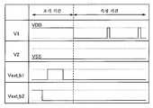
먼저, 오프 전류를 측정하기 위해 전위차를 부여하는 초기 기간의 개략에 대해서 설명한다. 초기 기간에서는, 트랜지스터(808)의 게이트에, 트랜지스터(808)를 온 상태로 하는 전위 Vext_b1을 입력하고, 트랜지스터(804)의 소스와 드레인 중 다른 쪽에 전기적으로 접속되는 노드 A(즉, 트랜지스터(808)의 소스와 드레인 중 한쪽, 용량 소자(802)의 다른 쪽 단자 및 트랜지스터(805)의 게이트에 전기적으로 접속된 노드)에 전위 V1을 공급한다. 여기서, 전위 V1은, 예를 들어 고전위이다. 트랜지스터(804)는 오프 상태이다.First, an outline of an initial period in which a potential difference is given to measure an off current will be described. In the initial period, a potential Vext_b1 for turning on the
그 후, 트랜지스터(808)의 게이트에, 트랜지스터(808)를 오프 상태로 하는 전위 Vext_b1을 입력하고, 트랜지스터(808)를 오프 상태로 한다. 트랜지스터(808)가 오프 상태로 된 후에, 전위 V1은 저전위로 설정된다. 트랜지스터(804)는 오프 상태로 남는다. 전위 V2은 전위 V1과 동일한 전위이다. 따라서, 초기 기간이 종료한다. 초기 기간이 종료되면, 노드 A와 트랜지스터(804)의 소스와 드레인 중 한쪽 사이에 전위차가 발생한다. 또한, 노드 A와 트랜지스터(808)의 소스와 드레인 중 다른 쪽 사이에 전위차가 발생한다. 따라서, 트랜지스터(804) 및 트랜지스터(808)를 통해 약간의 전하가 흐른다. 즉, 오프 전류가 발생한다.Thereafter, a potential Vext_b1 for turning off the
그 다음, 오프 전류의 측정 기간의 개략에 대해서 설명한다. 측정 기간에서는, 트랜지스터(804)의 소스와 드레인 중 한쪽의 전위(즉, V2), 및 트랜지스터(808)의 소스와 드레인 중 다른 쪽의 전위(즉, V1)는 저전위로 고정된다. 한편, 측정 기간 중에, 상기 노드 A의 전위는 고정되지 않는다(노드 A는 플로팅(floating) 상태이다). 따라서, 트랜지스터(804 및 808)를 통해 전하가 흐르고, 시간의 경과와 함께 노드 A에 유지되는 전하량이 변동한다. 노드 A에 유지되는 전하량의 변동에 따라, 노드 A의 전위가 변동한다. 즉, 출력 단자의 출력 전위 Vout도 변동한다.Next, the outline of the measurement period of the OFF current will be described. In the measurement period, one of the source and the drain of the transistor 804 (i.e., V2) and the other of the source and the drain of the transistor 808 (i.e., V1) are fixed at low potential. On the other hand, during the measurement period, the potential of the node A is not fixed (the node A is in a floating state). Therefore, charges flow through the
상기 전위차가 부여되는 초기 기간 및 그 후의 측정 기간에서의 전위들 간의 관계의 상세도(타이밍 차트)를 도 8에 도시한다.FIG. 8 shows a detailed diagram (timing chart) of the relationship between the potentials in the initial period in which the potential difference is given and in the subsequent measurement period.
초기 기간에서, 먼저, 전위 Vext_b2는 트랜지스터(804)가 온 상태로 되는 전위(고전위)로 설정된다. 따라서, 노드 A의 전위는 V2, 즉 저전위(VSS)가 된다. 반드시 노드 A에 저전위(Vss)를 부여할 필요는 없다는 점에 주목한다. 그 후에, 전위 Vext_b2는 트랜지스터(804)가 오프 상태로 되는 전위(저전위)로 설정되어, 트랜지스터(804)를 오프 상태로 한다. 그 다음, 전위 Vext_b1은 트랜지스터(808)가 온 상태로 되는 전위(고전위)로 설정된다. 따라서, 노드 A의 전위는 V1, 즉 고전위(VDD)가 된다. 그 후, Vext_b1은 트랜지스터(808)가 오프 상태로 되는 전위로 설정된다. 따라서, 노드 A가 플로팅 상태(floating state)로 되고, 초기 기간이 종료한다.In the initial period, first, the potential Vext_b2 is set to the potential (high potential) at which the
그 후의 측정 기간에서, 전위 V1 및 전위 V2는, 노드 A로 전하가 흐르게 되는 전위, 또는 노드 A로부터 전하가 흐르게 되는 전위로 설정된다. 여기에서는, 전위 V1 및 전위 V2 각각은 저전위(VSS)로 설정된다. 출력 전위 Vout을 측정하는 타이밍에서, 출력 회로를 동작시킬 필요가 생기기 때문에, 몇몇 경우에는 V1을 고전위(VDD)로 일시적으로 설정한다는 점에 주목한다. V1이 고전위(VDD)로 되는 기간은 짧기 때문에, 측정에 악영향을 주지 않는다.In the subsequent measurement period, the potential V1 and the potential V2 are set to a potential at which charge flows to the node A or a potential at which charges flow from the node A. Here, each of the potential V1 and the potential V2 is set to the low potential (VSS). Note that in some cases, V1 is temporarily set to the high potential (VDD) because it is necessary to operate the output circuit at the timing of measuring the output potential Vout. Since the period in which V1 becomes the high potential (VDD) is short, the measurement is not adversely affected.
상술한 바와 같이, 전위차를 부여하고, 측정 기간이 개시되면, 시간의 경과와 함께 노드 A에 유지되는 전하량이 변동하고, 이에 따라서 노드 A의 전위가 변동한다. 이것은, 트랜지스터(805)의 게이트의 전위가 변동하는 것을 의미하기 때문에, 시간이 경과함에 따라, 출력 단자의 출력 전위 Vout도 변화되는 것이다.As described above, when the potential difference is given and the measurement period is started, the amount of charge held in the node A changes with the elapse of time, and the potential of the node A fluctuates accordingly. This means that the potential of the gate of the
얻어진 출력 전위 Vout로부터 오프 전류를 산출하는 방법에 대해서, 이하에 설명한다.A method of calculating the off current from the obtained output potential Vout will be described below.
오프 전류의 산출에 앞서, 노드 A의 전위 VA와 출력 전위 Vout 간의 관계를 구해 둔다. 이러한 관계로 인해, 출력 전위 Vout을 이용하여 노드 A의 전위 VA를 얻을 수 있다. 상술한 관계로부터, 노드 A의 전위 VA는, 출력 전위 Vout의 함수로서 다음 식과 같이 나타낼 수 있다.Prior to the calculation of the off current, the relationship between the potential VA of the nodeA and the output potential Vout is obtained. Because of this relationship, the potential VA of the node A can be obtained by using the output potential Vout. From the above-described relationship, the potential VA of the node A can be expressed as a function of the output potential Vout as follows.

노드 A의 전하 QA는, 노드 A의 전위 VA, 노드 A에 접속되는 용량 CA, 및 상수(const)를 이용하여, 다음 식과 같이 나타낸다. 여기서, 노드 A에 접속되는 용량 CA는, 용량 소자(802)의 용량과 다른 용량의 합이다.The charge QA of the node A is expressed by the following equation using the potential VA of the node A, the capacitance CA connected to the nodeA , and a constant (const). Here, the capacitance CA connected to the node A is the sum of the capacitance of the

노드 A의 전류 IA는, 노드 A에 유입되는 전하(또는 노드 A로부터 유출되는 전하)를 시간 미분함으로써 얻어지기 때문에, 노드 A의 전류 IA는 다음 식과 같이 나타낸다.Since the current IA of the node A is obtained by time differentiating the charge (or the charge flowing out from the node A) flowing into the node A, the current IA of the node A is expressed by the following equation.

이와 같이, 노드 A에 접속되는 용량 CA, 및 출력 단자의 출력 전위 Vout으로부터, 노드 A의 전류 IA를 구할 수 있다.Thus, the current IA of the node A can be obtained from the capacitance CA connected to the node A and the output potential Vout of the output terminal.
상기 방법에 의해, 오프 상태에서 트랜지스터의 소스와 드레인 간을 흐르는 리크 전류(오프 전류)를 측정할 수 있다.With this method, it is possible to measure the leak current (off current) flowing between the source and the drain of the transistor in the OFF state.
여기에서, 채널 길이 L=10μm, 채널 폭 W=50μm의 고순도화된 산화물 반도체층을 각각 구비하는 트랜지스터(804) 및 트랜지스터(808)가 제작되었다. 병렬로 배치된 측정계(800)에서, 용량 소자(802)의 용량 값은 100fF, 1pF 및 3pF이다.Here, a
상술한 측정에서, VDD = 5 V이고 VSS = 0V라는 점에 주목한다. 측정 기간에서는, 전위 V1은 기본적으로 VSS이고, 10 내지 300초마다 100msec의 기간에서만 VDD로 설정되는 동안 Vout을 측정했다. 또한, 소자에 흐르는 전류 I의 산출에 사용되는 Δt는, 약 30000초이다.Note that in the measurements described above, VDD = 5V and VSS = 0V. In the measurement period, the potential V1 was basically VSS, and Vout was measured while being set to VDD only during a period of 100 msec every 10 to 300 seconds. Further,? T used for calculating the current I flowing through the device is about 30000 seconds.
도 9는 전류 측정시의 경과 시간(Time)과 출력 전위(Vout) 간의 관계를 나타낸다. 도 9로부터, 시간의 경과에 따라 전위가 변화되는 것을 확인할 수 있다.FIG. 9 shows the relationship between the elapsed time (Time) at the time of current measurement and the output potential Vout. From Fig. 9, it can be confirmed that the potential changes with the lapse of time.
도 10은 상기 전류 측정에 의해 산출된 실온(25℃)에서의 오프 전류를 도시한다. 도 10은 트랜지스터(804) 또는 트랜지스터(808)의 소스-드레인 전압 V와 오프 전류 I 간의 관계를 나타낸다. 도 10으로부터, 소스-드레인 전압이 4V일 때, 오프 전류가 약 40 zA/μm인 것을 알 수 있다. 또한, 소스-드레인 전압이 3.1V일 때, 오프 전류가 10 zA/μm 이하이다. 1 zA는 10-21A라는 점에 주목한다.10 shows the off current at room temperature (25 DEG C) calculated by the current measurement. 10 shows the relationship between the source-drain voltage V and the off-current I of the
상기 전류 측정에 의해 산출된 85℃의 온도에서의 오프 전류에 대해서 도 11에 도시한다. 도 11은 85℃의 온도에서 트랜지스터(804) 또는 트랜지스터(808)의 소스-드레인 전압 V와 오프 전류 I 간의 관계를 나타내는 것이다. 도 11로부터, 소스-드레인 전압이 3.1 V일 때, 오프 전류는 100 zA/μm 이하인 것을 알았다.The off current at a temperature of 85 캜 as calculated by the current measurement is shown in Fig. 11 shows the relationship between the source-drain voltage V and the off-current I of the
상술한 바에 의해, 고순도화된 산화물 반도체층을 구비하는 트랜지스터에서는, 오프 전류가 충분히 작아지는 것이 확인되었다.As described above, it was confirmed that the off current was sufficiently reduced in the transistor including the oxide semiconductor layer of high purity.
(표시 장치의 변형 예)(Modification of Display Device)
상술한 구성을 갖는 표시 장치는 본 발명의 한 실시 형태이며; 본 발명은 또한 표시 장치와는 상이한 표시 장치도 포함한다.The display device having the above-described configuration is an embodiment of the present invention; The present invention also includes a display device different from the display device.
<펄스 출력 회로의 변형 예>≪ Modified Example of Pulse Output Circuit >
예를 들어, 펄스 출력 회로는 도 3의 (a)에 도시한 펄스 출력 회로에 트랜지스터(50)이 추가로 제공되는 구성을 가질 수 있다(도 12의 (a) 참조). 트랜지스터(50)의 소스와 드레인 중 한쪽이 고 전원 전위선에 전기적으로 접속된다. 트랜지스터(50)의 소스와 드레인 중 다른 쪽이 트랜지스터(32)의 게이트, 트랜지스터(34)의 게이트, 트랜지스터(35)의 소스와 드레인 중 다른 쪽, 트랜지스터(36)의 소스와 드레인 중 다른 쪽, 트랜지스터(38)의 소스와 드레인 중 한쪽, 및 트랜지스터(41)의 게이트에 전기적으로 접속된다. 트랜지스터(50)의 게이트가 리셋 단자(Reset)에 전기적으로 접속된다. 리셋 단자에는, 수직 귀선 기간에 하이 레벨의 전위가 입력되고, 수직 귀선 기간 이외의 밖의 기간에는 로우 레벨의 전위가 입력된다는 점에 주목한다. 즉, 트랜지스터(50)는 수직 귀선 기간에 온 상태로 된다. 따라서, 수직 귀선 기간에 각 노드의 전위가 초기화될 수 있어, 오동작을 방지하는 것이 가능하다.For example, the pulse output circuit may have a configuration in which a
또한, 펄스 출력 회로는 도 3의 (a)에 도시한 펄스 출력 회로로부터, 트랜지스터(36)를 삭제한 구성을 가질 수 있다(도 12의 (b) 참조). 이러한 구성으로 인해, 펄스 출력 회로에 포함된 트랜지스터 수를 줄일 수 있다. 따라서, 해당 펄스 출력 회로의 레이아웃 면적의 축소, 수율의 향상 등을 도모할 수 있다.Further, the pulse output circuit may have a configuration in which the
펄스 출력 회로는 도 3의 (a)에 도시한 펄스 출력 회로로부터, 트랜지스터(39)를 삭제한 구성을 가질 수 있다(도 13의 (a) 참조). 이러한 구성으로, 펄스 출력 회로를 구성하는 트랜지스터 수를 저감할 수 있다. 따라서, 펄스 출력 회로의 레이아웃 면적의 축소, 수율의 향상 등을 도모할 수 있다.The pulse output circuit may have a configuration in which the
펄스 출력 회로는 도 3의 (a)에 도시한 펄스 출력 회로에, 트랜지스터(51)가 추가된 구성을 가질 수 있다(도 13의 (b) 참조). 트랜지스터(51)의 소스와 드레인 중 한쪽이 트랜지스터(33)의 게이트 및 트랜지스터(39)의 소스와 드레인 중 다른 쪽에 전기적으로 접속된다. 트랜지스터(51)의 소스와 드레인 중 다른 쪽이 트랜지스터(40)의 게이트에 전기적으로 접속된다. 트랜지스터(51)의 게이트가 고 전원 전위선에 전기적으로 접속된다. 트랜지스터(51)가 도 3의 (b) 및 (c)에 도시한 기간 t2 및 t3에 오프 상태로 된다는 점에 주목한다. 그 결과, 트랜지스터(51)을 포함하는 구성으로 인해, 기간 t2 및 t3에, 트랜지스터(33)의 게이트와 트랜지스터(40)의 게이트 간의 전기적인 접속을 차단하는 것이 가능하게 된다. 이하에서는, 펄스 출력 회로에 트랜지스터(51)가 포함된 구성(도 13의 (b) 참조)과 트랜지스터(51)가 포함되지 않은 구성(도 3의 (a) 참조)을 비교하여, 전자의 구성의 이점을 상세하게 서술한다.The pulse output circuit may have a configuration in which the
먼저, 트랜지스터(51)가 제공되지 않은 경우에 대해서 설명한다. 고 전원 전위(Vdd)와 저 전원 전위(Vss)를 반복하는 신호가 단자(25)에 입력되는 경우에는, 기간 t2와 t3에서, 단자(28)의 출력 신호 및 단자(26)의 출력 신호는, 둘 다 고 전원 전위(Vdd)가 된다. 이때, 트랜지스터(33 및 40)의 게이트의 전위(노드 A의 전위)는, 트랜지스터(33)의 소스와 게이트의 용량 결합 및 트랜지스터(40)의 소스와 게이트의 용량 결합에 의해, 고 전원 전위(Vdd)보다 높은 고전위가 된다. 한편, 단자(25)에 입력되는 신호가 저 전원 전위(Vss)에 고정되는 경우에는, 기간 t2 및 t3에서, 단자(28)의 출력 신호는 고 전원 전위(Vdd)가 되고, 단자(26)의 출력 신호는 저 전원 전위(Vss)가 된다. 이때, 트랜지스터(33 및 40)의 게이트의 전위(노드 A의 전위)는 트랜지스터(33)의 소스와 게이트의 용량 결합에 의해서만, 고 전원 전위(Vdd)보다 높은 고전위가 될 필요가 있다. 또한, 트랜지스터(40)는 주사선이 트랜지스터(40)에 의해 구동되기 때문에 트랜지스터(36)보다 채널 폭이 크게 되도록 설계되는 경우가 자주 있다. 즉, 트랜지스터(40)의 게이트는 용량 결합에 의해 전위가 상승할 때 큰 부하가 된다. 그 결과, 펄스 출력 회로를 동작시키기 위해서는, 트랜지스터(33)의 채널 길이에 대한 채널 폭의 비(W/L)를 크게 할 필요가 있다.First, a case where the
반면에, 트랜지스터(51)가 제공될 경우, 기간 t2 및 t3에서, 트랜지스터(33)의 게이트와 트랜지스터(40)의 게이트 간의 전기적인 접속이 차단된다. 그 결과, 트랜지스터(33)의 게이트의 전위만이 용량 결합에 의해 상승할 수 있다. 즉, 해당 용량 결합에서의 부하를 저감할 수 있다. 따라서, 펄스 출력 회로는 양호한 방식으로 동작할 수 있다. 또한, 트랜지스터(36)의 채널 길이에 대한 채널 폭의 비(W/L)를 크게 할 필요가 없으므로, 레이아웃 면적을 축소할 수 있다.On the other hand, when
도 13의 (b)에서는, 트랜지스터(51)의 게이트가 고 전원 전위선에 전기적으로 접속되는 구성에 대해서 도시하나; 대안적으로, 트랜지스터(51)의 게이트가 블록 단자(Block)에 전기적으로 접속되거나(도 14의 (a) 참조) 또는 단자(25)에 전기적으로 접속(도 14의 (b) 참조)될 수 있다는 점에 주목한다. 블록 단자(Block)에는, 제1 내지 제4 클록 신호(GCK1 내지 GCK4) 중 어느 하나와 동일한 신호가 단자(25)에 입력될 때에는 하이 레벨의 전위가 입력되고, 고정 전위(저 전원 전위(Vss))가 단자(25)에 입력될 때에는 로우 레벨의 전위가 입력되는 것이 바람직하다는 점에 주목한다. 즉, 트랜지스터(51)는 제1 내지 제4 클록 신호(GCK1 내지 GCK4) 중 어느 하나와 동일한 신호가 단자(25)에 입력될 때에는 온 상태로 되고, 고정 전위(저 전원 전위(Vss))가 단자(25)에 입력될 때에는 오프 상태로 되도록 제어된다. 따라서, 트랜지스터(33)의 게이트와 트랜지스터(40)의 게이트 간의 전기적인 접속이 차단되는 타이밍을 빨리 할 수 있다. 또한, 트랜지스터(51)의 게이트가 단자(25)에 전기적으로 접속되는 구성(도 14의 (b) 참조)은, 신호를 새롭게 추가할 필요가 없다는 점에서 바람직하다.13B shows a configuration in which the gate of the
<트랜지스터의 변형 예>≪ Modification example of transistor &
상술한 소정의 표시 장치에서, 화소(16)에 제공된 트랜지스터(17)로서, 채널 에치형 구조로 칭해지는 보텀 게이트 구조(도 5 참조)의 트랜지스터(211)를 사용하지만, 트랜지스터(17)는 이러한 구조를 갖는 것으로 한정되지 않는다. 예를 들어, 도 15의 (a) 내지 (c)에 도시된 트랜지스터를 사용할 수 있다.In the above-described predetermined display device, the
도 15의 (a)에 도시된 트랜지스터(510)는 채널 보호형(채널 스톱형이라고도 함)이라고 칭해지는 보텀 게이트 구조의 유형을 갖는다.The
트랜지스터(510)는, 절연면을 갖는 기판(220) 위에, 게이트층(221), 게이트 절연층(222), 산화물 반도체층(223), 산화물 반도체층(223)의 채널 형성 영역을 덮는 채널 보호층으로서 기능하는 절연층(511), 소스층(224a) 및 드레인층(224b)을 포함한다. 또한, 보호 절연층(226)은 소스층(224a), 드레인층(224b) 및 절연층(511)을 덮도록 형성된다.The
도 15의 (b)에 도시된 트랜지스터(520)는 보텀 게이트형의 트랜지스터이다. 트랜지스터(520)는, 절연면을 갖는 기판(220) 위에, 게이트층(221), 게이트 절연층(222), 소스층(224a), 드레인층(224b) 및 산화물 반도체층(223)을 포함한다. 또한, 소스층(224a) 및 드레인층(224b)을 덮고 있고, 산화물 반도체층(223)에 접하여 있는 절연층(225)이 제공된다. 절연층(225) 위에는 보호 절연층(226)이 제공된다.The
트랜지스터(520)에서, 게이트 절연층(222)은 기판(220) 및 게이트층(221) 위에 접하여 제공되고, 게이트 절연층(222) 위에는 소스층(224a) 및 드레인층(224b)이 접하여 제공된다. 또한, 게이트 절연층(222), 소스층(224a) 및 드레인층(224b) 위에는 산화물 반도체층(223)이 제공된다.In the
도 15의 (c)에 도시된 트랜지스터(530)는 톱 게이트 트랜지스터의 유형이다. 트랜지스터(530)는 절연면을 갖는 기판(220) 위에, 절연층(531), 산화물 반도체층(223), 소스층(224a) 및 드레인층(224b), 게이트 절연층(222), 및 게이트층(221)을 포함한다. 배선층(532a) 및 배선층(532b)은 소스층(224a) 및 드레인층(224b)에 각각 접하여 제공되고, 소스층(224a) 및 드레인층(224b)에 각각 전기적으로 접속된다.The
절연층(511 및 531)으로서, 산화 실리콘막, 산화 질화 실리콘막, 산화 알루미늄막 또는 산화 질화 알루미늄막으로 대표되는 무기 절연막을 이용할 수 있다. 또한, 배선층(532a) 및 배선층(532b)에 사용되는 도전막은 예를 들어, Al, Cr, Cu, Ta, Ti, Mo 및 W로부터 선택된 원소, 또는 임의의 이들 원소를 성분으로 포함하는 합금이나, 임의의 이들 원소를 조합한 합금막 등을 이용하여 형성될 수 있다. Al, Cu 등의 금속층의 상부면 또는 하부면 중 하나 또는 둘 다의 위에 Ti, Mo, W 등의 고융점 금속층을 적층한 구성이 채택될 수 있다. Al막에 힐록(hillocks) 및 위스커(whiskers)의 발생을 방지하는 원소(예를 들면, Si, Nd 또는 Sc)이 첨가되어 있는 Al 재료를 이용함으로써, 내열성을 향상시키는 것이 가능하게 된다.As the insulating
(표시 장치를 탑재한 각종 전자 기기)(Various electronic apparatuses equipped with a display device)
이하에서는, 본 명세서에서 개시되는 소정의 표시 장치를 탑재한 전자 기기의 예에 대해서 도 16의 (a) 내지 (f)를 참조하여 설명한다.Hereinafter, an example of an electronic apparatus equipped with a certain display device disclosed in this specification will be described with reference to Figs. 16A to 16F.
도 16의 (a)는, 본체(2201), 하우징(2202), 표시부(2203), 키보드(2204) 등을 포함하는 노트북 퍼스널 컴퓨터를 도시한다.16A shows a notebook personal computer including a
도 16의 (b)는, 휴대 정보 단말(PDA)을 도시하는 도면이다. 본체(2211)에는 표시부(2213), 외부 인터페이스(2215), 조작 버튼(2214) 등이 제공된다. PDA 조작용 부속품으로서 스타일러스(stylus; 2212)가 제공된다.16 (b) is a diagram showing a portable information terminal (PDA). The
도 16의 (c)는 전자 페이퍼의 일례로서, 전자 서적 리더(2220)를 도시한다. 전자 서적 리더(2220)는 하우징(2221) 및 하우징(2223)의 2개의 하우징을 포함한다. 하우징(2221) 및 하우징(2223)은 축부(2237)에 의해 일체로 되어 있어, 상기 축부(2237)를 축으로 해서 전자 서적 리더(2220)가 개폐 동작을 할 수 있다. 이러한 구성에 의해, 전자 서적 리더(2220)는 종이 서적처럼 사용될 수 있다.FIG. 16C shows an
하우징(2221)에는 표시부(2225)가 내장되고, 하우징(2223)에는 표시부(2227)가 내장되어 있다. 표시부(2225) 및 표시부(2227)는 하나의 화상 또는 다른 화상들을 표시할 수 있다. 표시부(2225) 및 표시부(2227)가 다른 화상들을 표시하는 경우에, 예를 들어 우측 표시부(도 16의 (c)에서 표시부(2225))는 문장을 표시할 수 있고, 좌측 표시부(도 16의 (c)에서 표시부(2227))는 그림을 표시할 수 있다.The
또한, 도 16의 (c)에서, 하우징(2221)에는 조작부 등이 제공된다. 예를 들어, 하우징(2221)에는 전원 스위치(2231), 조작 키(2233) 및 스피커(2235)가 제공된다. 페이지는 조작 키(2233)에 의해 넘겨질 수 있다. 상부에 표시부가 제공되는 하우징의 표면에는 키보드, 포인팅 디바이스 등도 제공될 수 있다는 점에 주목한다. 하우징의 이면이나 측면에는, 외부 접속용 단자(예를 들면, 이어폰 단자, USB 단자, 또는 AC 어댑터 및 USB 케이블 등의 각종 케이블과 접속 가능한 단자), 기록 매체 삽입부 등이 제공될 수 있다. 또한, 전자 서적 리더(2220)는 전자 사전으로서의 기능을 가질 수 있다.16 (c), the
전자 서적 리더(2220)는 무선으로 정보를 송수신할 수 있다. 무선 통신을 통해, 전자 서적 서버로부터, 원하는 서적 데이터 등을 구입하고 다운로드할 수 있다. The
전자 페이퍼는, 데이터를 표시하는 것이라면 다양한 분야에 적용하는 것이 가능하다는 점에 주목한다. 예를 들어, 전자 페이퍼는 전자 서적 리더 이외에도, 포스터(poster), 기차 등의 차내 광고, 신용 카드 등의 각종 카드에서의 표시 등에 사용할 수 있다.Note that the electronic paper can be applied to various fields as long as it displays data. For example, electronic papers can be used for display on various cards such as posters, in-car advertisements such as trains, credit cards, etc., in addition to electronic book readers.
도 16의 (d)는 휴대 전화기를 도시하는 도면이다. 휴대 전화기는 하우징(2240) 및 하우징(2241)의 2개의 하우징을 포함한다. 하우징(2241)에는 표시 패널(2242), 스피커(2243), 마이크로폰(2244), 포인팅 디바이스(2246), 카메라용 렌즈(2247), 외부 접속 단자(2248) 등이 제공된다. 하우징(2240)에는 휴대 전화기를 충전하는 태양 전지(2249), 외부 메모리 슬롯(2250) 등이 제공된다. 또한, 안테나는 하우징(2241)에 내장되어 있다.FIG. 16D is a diagram showing a cellular phone. The cellular phone includes two housings, a
표시 패널(2242)은 터치 패널 기능을 구비하고 있다. 도 16의 (d)에서, 화상으로서 표시된 복수의 조작 키(2245)를 점선으로 나타내고 있다. 휴대 전화기는 태양 전지(2249)로부터 출력되는 전압을 각 회로에 필요한 전압으로 승압하기 위한 승압 회로를 포함하고 있다는 점에 주목한다. 또한, 상기 구성 외에, 휴대 전화기는 비접촉 IC 칩, 소형 기록 장치 등을 포함할 수 있다.The
표시 패널(2242)의 표시 방향은 응용 모드에 따라 적절히 변화된다. 또한, 표시 패널(2242)과 동일면 위에 카메라용 렌즈(2247)를 구비하고 있기 때문에, 휴대 전화기는 영상 전화(video phone)로 사용될 수 있다. 스피커(2243) 및 마이크로폰(2244)은 음성 통화뿐만 아니라, 영상 전화, 녹음, 음재생 등에 사용될 수 있다. 따라서, 도 16의 (d)와 같이 전개된 상태의 하우징(2240)과 하우징(2241)은 하나가 다른 하나와 겹치도록 슬라이드식으로 동작할 수 있다. 따라서, 휴대 전화기의 사이즈는 휴대에 알맞게 소형화가 가능하다.The display direction of the
외부 접속 단자(2248)는 AC 어댑터 또는 USB 케이블 등의 각종 케이블과 접속 가능하며, 이는 휴대 전화기의 충전이나 데이터 통신을 가능하게 한다. 또한, 외부 메모리 슬롯(2250)에 기록 매체를 삽입함으로써, 보다 대량인 데이터의 보존 및 이동이 가능하다. 또한, 상기 기능 외에, 휴대 전화기는 적외선 통신 기능, 텔레비전 수신 기능 등을 구비할 수 있다.The
도 16의 (e)는 디지털 카메라를 도시하는 도면이다. 디지털 카메라는 본체(2261), 표시부(A)(2267), 접안부(eyepiece; 2263), 조작 스위치(2264), 표시부(B)(2265), 배터리(2266) 등으로 구성되어 있다.FIG. 16 (e) is a diagram showing a digital camera. The digital camera includes a
도 16의 (f)는 텔레비전 세트를 도시하는 도면이다. 텔레비전 세트(2270)에서는, 하우징(2271)에 표시부(2273)가 내장되어 있다. 표시부(2273)는 화상을 표시하는 것이 가능하다. 여기서, 스탠드(2275)에 의해 하우징(2271)이 지지된다.16 (f) is a diagram showing a television set. In the
텔레비전 세트(2270)는 하우징(2271)의 조작 스위치 또는 별개의 원격 컨트롤러(2280)에 의해 조작될 수 있다. 원격 컨트롤러(2280)의 조작 키(2279)에 의해, 채널이나 음량이 제어될 수 있고, 표시부(2273)에 표시되는 화상이 제어될 수 있다. 또한, 원격 컨트롤러(2280)는 해당 원격 컨트롤러(2280)로부터 출력되는 데이터를 표시하는 표시부(2277)를 포함할 수 있다.The
또한, 텔레비전 세트(2270)에는 수신기나 모뎀 등이 구비되는 것이 바람직하다. 수신기에 의해, 일반 텔레비전 방송을 수신할 수 있다. 또한, 텔레비전 세트가 모뎀을 통해서 유선 또는 무선으로 통신 네트워크에 접속하면, 일방향(송신자에게서 수신자로) 또는 쌍방향(송신자와 수신자 간, 혹은 수신자 간)의 정보 통신을 행하는 것이 가능하다.It is preferable that the
본 출원은 2010년 3월 12일 일본 특허청에 출원된 일본 특허 출원 번호 2010-056464를 기초로 하며, 그 전체 내용은 본 명세서에 참조로 원용된다.This application is based on Japanese Patent Application No. 2010-056464 filed in Japan on March 12, 2010, the entire contents of which are incorporated herein by reference.
10 : 화소부
11 : 주사선 구동 회로
12 : 신호선 구동 회로
13 : 컨트롤러
14 : 주사선
15 : 신호선
16 : 화소
17 : 트랜지스터
18 : 용량 소자
19 : 액정 소자
20_1 내지 20_m : 펄스 출력 회로
20_x : 펄스 출력 회로
21 내지 28 : 단자
31 내지 41 : 트랜지스터
50 : 트랜지스터
51 : 트랜지스터
131 : 신호 생성 회로
132 : 기억 회로
133 : 비교 회로
134 : 선택 회로
135 : 표시 제어 회로
136 : 메모리
211 : 트랜지스터
220 : 기판
221 : 게이트층
222 : 게이트 절연층
223 : 산화물 반도체층
224a : 소스층
224b : 드레인층
225 : 절연층
226 : 보호 절연층
510 : 트랜지스터
511 : 절연층
520 : 트랜지스터
530 : 트랜지스터
531 : 절연층
532a : 배선층
532b : 배선층
800 : 측정계
802 : 용량 소자
804 : 트랜지스터
805 : 트랜지스터
806 : 트랜지스터
808 : 트랜지스터
2201 : 본체
2202 : 하우징
2203 : 표시부
2204 : 키보드
2211 : 본체
2212 : 스타일러스
2213 : 표시부
2214 : 조작 버튼
2215 : 외부 인터페이스
2220 : 전자 서적 리더
2221 : 하우징
2223 : 하우징
2225 : 표시부
2227 : 표시부
2231 : 전원 스위치
2233 : 조작 키
2235 : 스피커
2237 : 축부
2240 : 하우징
2241 : 하우징
2242 : 표시 패널
2243 : 스피커
2244 : 마이크로폰
2245 : 조작 키
2246 : 포인팅 디바이스
2247 : 카메라용 렌즈
2248 : 외부 접속 단자
2249 : 태양 전지
2250 : 외부 메모리 슬롯
2261 : 본체
2263 : 접안부
2264 : 조작 스위치
2265 : 표시부(B)
2266 : 배터리
2267 : 표시부(A)
2270 : 텔레비전 세트
2271 : 하우징
2273 : 표시부
2275 : 스탠드
2277 : 표시부
2279 : 조작 키
2280 : 원격 컨트롤러10:
11: scanning line driving circuit
12: Signal line driving circuit
13: Controller
14: Scanning line
15: Signal line
16: pixel
17:
18: Capacitive element
19: liquid crystal element
20_1 to 20_m: pulse output circuit
20_x: Pulse output circuit
21 to 28: terminal
31 to 41: transistor
50: transistor
51: transistor
131: Signal Generation Circuit
132: memory circuit
133: comparison circuit
134: selection circuit
135: Display control circuit
136: Memory
211: transistor
220: substrate
221: gate layer
222: gate insulating layer
223: oxide semiconductor layer
224a: source layer
224b: drain layer
225: Insulation layer
226: Protective insulating layer
510: transistor
511: Insulating layer
520: transistor
530: transistor
531: Insulating layer
532a: wiring layer
532b:
800: Measuring system
802: capacitive element
804: Transistor
805: Transistor
806: Transistor
808: Transistor
2201:
2202: Housing
2203:
2204: Keyboard
2211:
2212: Stylus
2213:
2214: Operation button
2215: External interface
2220: Electronic Book Reader
2221: housing
2223: Housing
2225:
2227:
2231: Power switch
2233: Operation keys
2235: Speaker
2237:
2240: Housing
2241: Housing
2242: Display panel
2243: Speaker
2244: microphone
2245: Operation keys
2246: Pointing device
2247: Camera lens
2248: External connection terminal
2249: Solar cell
2250: External memory slot
2261:
2263: Eyepiece
2264: Operation switch
2265: Display portion (B)
2266: Battery
2267: Display portion (A)
2270: Television sets
2271: Housing
2273:
2275: Stand
2277:
2279: Operation keys
2280: Remote controller
Claims (3)
Translated fromKorean화소부와, 주사선 구동 회로를 가지고,
상기 화소부는, 제1 화소를 포함하는 복수의 화소를 가지고,
상기 주사선 구동 회로는, 제1 배선과, 제2 배선과, 제1 펄스 출력 회로 및 제2 펄스 출력 회로를 포함하는 복수의 펄스 출력 회로를 가지고,
상기 제1 펄스 출력 회로는, 제1 트랜지스터와, 제2 트랜지스터를 가지고,
상기 제1 배선은, 상기 제1 트랜지스터를 통해 상기 제1 화소와 전기적으로 접속되고,
상기 제2 배선은, 상기 제2 트랜지스터를 통해 상기 제2 펄스 출력 회로와 전기적으로 접속되고,
상기 제1 모드에서, 상기 제2 배선에 제1 클록 신호를 입력하는 것과 함께, 상기 제1 배선에 상기 제1 클록 신호와 동일한 신호를 입력하고,
상기 제2 모드에서, 상기 제2 배선에 상기 제1 클록 신호를 입력하는 것과 함께, 상기 제1 배선에 상기 제1 클록 신호와 동일한 신호 또는 고정 전위를 선택적으로 입력하고,
상기 제3 모드에서, 상기 화소부에 화상을 유지한 채, 상기 주사선 구동 회로의 동작을 정지시키고,
상기 제1 화소는, 제3 트랜지스터를 가지고,
상기 제3 트랜지스터는, 산화물 반도체층에 채널 형성 영역을 가지고,
상기 제3 트랜지스터는 85℃의 온도 환경 하에서의 소스-드레인 전압이 3.1V인 조건에서, 오프 전류가 100zA/㎛ 이하인, 표시 장치.A display device capable of performing the first to third modes,
A pixel portion, and a scanning line driving circuit,
Wherein the pixel portion has a plurality of pixels including a first pixel,
The scanning line driving circuit has a plurality of pulse output circuits including a first wiring, a second wiring, a first pulse output circuit and a second pulse output circuit,
Wherein the first pulse output circuit includes a first transistor and a second transistor,
The first wiring is electrically connected to the first pixel through the first transistor,
The second wiring is electrically connected to the second pulse output circuit through the second transistor,
The first clock signal is input to the second wiring and the same signal as the first clock signal is input to the first wiring in the first mode,
The first clock signal is input to the second wiring and the signal or the fixed potential, which is the same as the first clock signal, is selectively input to the first wiring,
In the third mode, the operation of the scanning line driving circuit is stopped while the image is held in the pixel portion,
Wherein the first pixel has a third transistor,
Wherein the third transistor has a channel forming region in the oxide semiconductor layer,
Wherein the third transistor has an off current of 100 zA / 占 퐉 or less under the condition that the source-drain voltage is 3.1 V under a temperature environment of 85 占 폚.
상기 제3 모드에서, 상기 제1 화소에 포함된 액정 소자에 인가되는 전압을 반전하는, 표시 장치.The method according to claim 1,
And in the third mode, inverts the voltage applied to the liquid crystal element included in the first pixel.
Applications Claiming Priority (3)
| Application Number | Priority Date | Filing Date | Title |
|---|---|---|---|
| JPJP-P-2010-056464 | 2010-03-12 | ||
| JP2010056464 | 2010-03-12 | ||
| PCT/JP2011/054059WO2011111531A1 (en) | 2010-03-12 | 2011-02-17 | Display device |
Related Parent Applications (1)
| Application Number | Title | Priority Date | Filing Date |
|---|---|---|---|
| KR1020127026490ADivisionKR101798260B1 (en) | 2010-03-12 | 2011-02-17 | Display device |
Publications (2)
| Publication Number | Publication Date |
|---|---|
| KR20170127062A KR20170127062A (en) | 2017-11-20 |
| KR101975140B1true KR101975140B1 (en) | 2019-05-03 |
Family
ID=44559514
Family Applications (2)
| Application Number | Title | Priority Date | Filing Date |
|---|---|---|---|
| KR1020177032451AExpired - Fee RelatedKR101975140B1 (en) | 2010-03-12 | 2011-02-17 | Display device |
| KR1020127026490AExpired - Fee RelatedKR101798260B1 (en) | 2010-03-12 | 2011-02-17 | Display device |
Family Applications After (1)
| Application Number | Title | Priority Date | Filing Date |
|---|---|---|---|
| KR1020127026490AExpired - Fee RelatedKR101798260B1 (en) | 2010-03-12 | 2011-02-17 | Display device |
Country Status (5)
| Country | Link |
|---|---|
| US (1) | US8836686B2 (en) |
| JP (9) | JP5947488B2 (en) |
| KR (2) | KR101975140B1 (en) |
| TW (3) | TWI541786B (en) |
| WO (1) | WO2011111531A1 (en) |
Families Citing this family (14)
| Publication number | Priority date | Publication date | Assignee | Title |
|---|---|---|---|---|
| JP5436324B2 (en) | 2010-05-10 | 2014-03-05 | 三菱電機株式会社 | Shift register circuit |
| KR102615409B1 (en) | 2010-05-21 | 2023-12-20 | 가부시키가이샤 한도오따이 에네루기 켄큐쇼 | Pulse output circuit, shift register, and display device |
| US8718224B2 (en)* | 2011-08-05 | 2014-05-06 | Semiconductor Energy Laboratory Co., Ltd. | Pulse signal output circuit and shift register |
| JP2013093565A (en) | 2011-10-07 | 2013-05-16 | Semiconductor Energy Lab Co Ltd | Semiconductor device |
| KR101396942B1 (en) | 2012-03-21 | 2014-05-19 | 엘지디스플레이 주식회사 | Gate driving unit and liquid crystal display device comprising the same |
| TWI635501B (en)* | 2012-07-20 | 2018-09-11 | 半導體能源研究所股份有限公司 | Pulse output circuit, display device, and electronic device |
| US9041453B2 (en) | 2013-04-04 | 2015-05-26 | Semiconductor Energy Laboratory Co., Ltd. | Pulse generation circuit and semiconductor device |
| US9461126B2 (en) | 2013-09-13 | 2016-10-04 | Semiconductor Energy Laboratory Co., Ltd. | Transistor, clocked inverter circuit, sequential circuit, and semiconductor device including sequential circuit |
| TWI500015B (en)* | 2014-06-20 | 2015-09-11 | Au Optronics Corp | Bi-direction circuit, gate driver and testing circuit utilizing the same |
| KR102611213B1 (en)* | 2016-06-22 | 2023-12-07 | 삼성디스플레이 주식회사 | Display device |
| KR102490300B1 (en)* | 2016-07-29 | 2023-01-20 | 엘지디스플레이 주식회사 | Display device, gate driver and driving method thereof |
| US20210287621A1 (en)* | 2016-09-27 | 2021-09-16 | Sharp Kabushiki Kaisha | Display panel |
| WO2020058799A1 (en) | 2018-09-21 | 2020-03-26 | 株式会社半導体エネルギー研究所 | Flip-flop circuit, drive circuit, display panel, display device, input/output device, and information processing device |
| CN112596430A (en)* | 2020-12-03 | 2021-04-02 | 深圳市道和实业有限公司 | Handwriting board circuit for accurate display of electronic book |
Citations (4)
| Publication number | Priority date | Publication date | Assignee | Title |
|---|---|---|---|---|
| JP2008058939A (en) | 2006-09-01 | 2008-03-13 | Samsung Electronics Co Ltd | Display device, driving method thereof, and switching method of screen display mode |
| JP2008140490A (en) | 2006-12-04 | 2008-06-19 | Seiko Epson Corp | Shift register, scanning line driving circuit, electro-optical device, and electronic apparatus |
| WO2009028716A1 (en) | 2007-08-30 | 2009-03-05 | Sharp Kabushiki Kaisha | Shift register, display driver and display |
| JP2010056542A (en)* | 2008-07-31 | 2010-03-11 | Semiconductor Energy Lab Co Ltd | Semiconductor device and method of manufacturing semiconductor device |
Family Cites Families (33)
| Publication number | Priority date | Publication date | Assignee | Title |
|---|---|---|---|---|
| JP3476241B2 (en) | 1994-02-25 | 2003-12-10 | 株式会社半導体エネルギー研究所 | Display method of active matrix type display device |
| JP3617896B2 (en)* | 1997-02-12 | 2005-02-09 | 株式会社東芝 | Liquid crystal display device and driving method |
| KR100430099B1 (en)* | 1999-03-02 | 2004-05-03 | 엘지.필립스 엘시디 주식회사 | Shift Register Circuit |
| JP3767292B2 (en)* | 1999-12-22 | 2006-04-19 | セイコーエプソン株式会社 | Driving method of display device |
| TW494382B (en)* | 2000-03-22 | 2002-07-11 | Toshiba Corp | Display apparatus and driving method of display apparatus |
| JP4537526B2 (en)* | 2000-03-22 | 2010-09-01 | 東芝モバイルディスプレイ株式会社 | Liquid crystal display device and driving method thereof |
| JP2002140052A (en)* | 2000-08-23 | 2002-05-17 | Semiconductor Energy Lab Co Ltd | Portable information device and its driving method |
| JP2002169499A (en)* | 2000-11-30 | 2002-06-14 | Sanyo Electric Co Ltd | Driving method of display panel and driving controller of display panel |
| JP4425547B2 (en)* | 2003-01-17 | 2010-03-03 | 株式会社半導体エネルギー研究所 | Pulse output circuit, shift register, and electronic device |
| US7369111B2 (en)* | 2003-04-29 | 2008-05-06 | Samsung Electronics Co., Ltd. | Gate driving circuit and display apparatus having the same |
| JP4105132B2 (en)* | 2003-08-22 | 2008-06-25 | シャープ株式会社 | Display device drive circuit, display device, and display device drive method |
| JP4662014B2 (en)* | 2003-09-29 | 2011-03-30 | 東北パイオニア株式会社 | Driving device and driving method of light emitting display panel |
| TWI258724B (en)* | 2003-10-28 | 2006-07-21 | Samsung Electronics Co Ltd | Circuits and methods providing reduced power consumption for driving flat panel displays |
| JP4993544B2 (en)* | 2005-03-30 | 2012-08-08 | 三菱電機株式会社 | Shift register circuit |
| KR101152129B1 (en) | 2005-06-23 | 2012-06-15 | 삼성전자주식회사 | Shift register for display device and display device including shift register |
| JP5064747B2 (en)* | 2005-09-29 | 2012-10-31 | 株式会社半導体エネルギー研究所 | Semiconductor device, electrophoretic display device, display module, electronic device, and method for manufacturing semiconductor device |
| EP1770788A3 (en)* | 2005-09-29 | 2011-09-21 | Semiconductor Energy Laboratory Co., Ltd. | Semiconductor device having oxide semiconductor layer and manufacturing method thereof |
| US7612770B2 (en)* | 2005-12-15 | 2009-11-03 | Tpo Displays Corp. | Systems for displaying images |
| JP4728816B2 (en)* | 2006-01-13 | 2011-07-20 | 東芝モバイルディスプレイ株式会社 | Display device, driving method thereof, and terminal device |
| JP5525685B2 (en)* | 2006-10-17 | 2014-06-18 | 株式会社半導体エネルギー研究所 | Semiconductor device and electronic equipment |
| TWI511116B (en)* | 2006-10-17 | 2015-12-01 | Semiconductor Energy Lab | Pulse output circuit, shift register and display device |
| JP2008224924A (en)* | 2007-03-12 | 2008-09-25 | Seiko Epson Corp | Liquid crystal device, driving method thereof, and electronic apparatus |
| JP2008287134A (en)* | 2007-05-21 | 2008-11-27 | Seiko Epson Corp | Pulse output circuit, shift register, scanning line driving circuit, data line driving circuit, electro-optical device, and electronic apparatus |
| KR101415561B1 (en)* | 2007-06-14 | 2014-08-07 | 삼성디스플레이 주식회사 | Thin film transistor display panel and manufacturing method thereof |
| JP4968681B2 (en)* | 2007-07-17 | 2012-07-04 | Nltテクノロジー株式会社 | Semiconductor circuit, display device using the same, and driving method thereof |
| EP2189988B1 (en) | 2007-09-12 | 2012-12-12 | Sharp Kabushiki Kaisha | Shift register |
| EP2189987B1 (en)* | 2007-09-12 | 2013-02-13 | Sharp Kabushiki Kaisha | Shift register |
| CN101897031B (en)* | 2007-12-13 | 2013-04-17 | 出光兴产株式会社 | Field-effect transistor using oxide semiconductor and manufacturing method thereof |
| KR100963003B1 (en)* | 2008-02-05 | 2010-06-10 | 삼성모바일디스플레이주식회사 | Thin film transistor, its manufacturing method, and flat panel display device comprising thin film transistor |
| JP2009205706A (en)* | 2008-02-26 | 2009-09-10 | Sony Corp | Shift register circuit, display unit, and electronic device |
| JP2009288562A (en)* | 2008-05-29 | 2009-12-10 | Casio Comput Co Ltd | Drive control circuit, electronic equipment, and driving method of the drive control circuit |
| TWI469354B (en)* | 2008-07-31 | 2015-01-11 | Semiconductor Energy Lab | Semiconductor device and method of manufacturing same |
| KR101544051B1 (en)* | 2009-02-17 | 2015-08-13 | 삼성디스플레이 주식회사 | Gate line driving method, gate line driving circuit performing the same, and display device including the same |
- 2011
- 2011-02-17KRKR1020177032451Apatent/KR101975140B1/ennot_activeExpired - Fee Related
- 2011-02-17WOPCT/JP2011/054059patent/WO2011111531A1/enactiveApplication Filing
- 2011-02-17KRKR1020127026490Apatent/KR101798260B1/ennot_activeExpired - Fee Related
- 2011-03-07JPJP2011049377Apatent/JP5947488B2/ennot_activeExpired - Fee Related
- 2011-03-09USUS13/044,130patent/US8836686B2/ennot_activeExpired - Fee Related
- 2011-03-10TWTW100108101Apatent/TWI541786B/ennot_activeIP Right Cessation
- 2011-03-10TWTW105110569Apatent/TWI591614B/enactive
- 2011-03-10TWTW106113501Apatent/TWI615831B/enactive
- 2016
- 2016-02-05JPJP2016021011Apatent/JP6074077B2/enactiveActive
- 2017
- 2017-01-05JPJP2017000335Apatent/JP2017111449A/ennot_activeWithdrawn
- 2019
- 2019-03-22JPJP2019054604Apatent/JP2019144561A/ennot_activeWithdrawn
- 2020
- 2020-12-21JPJP2020211223Apatent/JP2021061085A/ennot_activeWithdrawn
- 2022
- 2022-11-22JPJP2022186568Apatent/JP2023024457A/ennot_activeWithdrawn
- 2023
- 2023-11-29JPJP2023201706Apatent/JP2024037759A/ennot_activeWithdrawn
- 2025
- 2025-03-07JPJP2025036011Apatent/JP2025085658A/enactivePending
- 2025-06-12JPJP2025098209Apatent/JP2025129161A/enactivePending
Patent Citations (4)
| Publication number | Priority date | Publication date | Assignee | Title |
|---|---|---|---|---|
| JP2008058939A (en) | 2006-09-01 | 2008-03-13 | Samsung Electronics Co Ltd | Display device, driving method thereof, and switching method of screen display mode |
| JP2008140490A (en) | 2006-12-04 | 2008-06-19 | Seiko Epson Corp | Shift register, scanning line driving circuit, electro-optical device, and electronic apparatus |
| WO2009028716A1 (en) | 2007-08-30 | 2009-03-05 | Sharp Kabushiki Kaisha | Shift register, display driver and display |
| JP2010056542A (en)* | 2008-07-31 | 2010-03-11 | Semiconductor Energy Lab Co Ltd | Semiconductor device and method of manufacturing semiconductor device |
Also Published As
| Publication number | Publication date |
|---|---|
| TWI541786B (en) | 2016-07-11 |
| US8836686B2 (en) | 2014-09-16 |
| JP2021061085A (en) | 2021-04-15 |
| KR20130006655A (en) | 2013-01-17 |
| TW201730872A (en) | 2017-09-01 |
| JP2017111449A (en) | 2017-06-22 |
| JP2011209714A (en) | 2011-10-20 |
| JP2023024457A (en) | 2023-02-16 |
| JP2025085658A (en) | 2025-06-05 |
| TW201137850A (en) | 2011-11-01 |
| JP2019144561A (en) | 2019-08-29 |
| JP2016136447A (en) | 2016-07-28 |
| TWI591614B (en) | 2017-07-11 |
| KR101798260B1 (en) | 2017-11-15 |
| JP2025129161A (en) | 2025-09-04 |
| JP6074077B2 (en) | 2017-02-01 |
| KR20170127062A (en) | 2017-11-20 |
| TWI615831B (en) | 2018-02-21 |
| TW201638927A (en) | 2016-11-01 |
| US20110221734A1 (en) | 2011-09-15 |
| WO2011111531A1 (en) | 2011-09-15 |
| JP2024037759A (en) | 2024-03-19 |
| JP5947488B2 (en) | 2016-07-06 |
Similar Documents
| Publication | Publication Date | Title |
|---|---|---|
| KR101975140B1 (en) | Display device | |
| KR102435828B1 (en) | Semiconductor device | |
| JP6224150B2 (en) | Semiconductor devices, display modules, electronic equipment | |
| KR101712340B1 (en) | Driver circuit, display device including the driver circuit, and electronic device including the display device | |
| TWI630599B (en) | Display device and electronic device including the same | |
| JP5809442B2 (en) | Display device | |
| US8633889B2 (en) | Display device, driving method thereof, and electronic appliance | |
| CN102024412A (en) | Semiconductor device and display device | |
| US8847933B2 (en) | Display device | |
| KR20120023548A (en) | Liquid crystal display device and driving method of the same | |
| CN102884477A (en) | Liquid crystal display device and method for driving the same | |
| KR100761612B1 (en) | Electro-optical device and electronic apparatus | |
| US20040246214A1 (en) | Liquid crystal display and sampling circuit therefor |
Legal Events
| Date | Code | Title | Description |
|---|---|---|---|
| A107 | Divisional application of patent | ||
| A201 | Request for examination | ||
| PA0104 | Divisional application for international application | St.27 status event code:A-0-1-A10-A16-div-PA0104 St.27 status event code:A-0-1-A10-A18-div-PA0104 | |
| PA0201 | Request for examination | St.27 status event code:A-1-2-D10-D11-exm-PA0201 | |
| PG1501 | Laying open of application | St.27 status event code:A-1-1-Q10-Q12-nap-PG1501 | |
| E902 | Notification of reason for refusal | ||
| PE0902 | Notice of grounds for rejection | St.27 status event code:A-1-2-D10-D21-exm-PE0902 | |
| E13-X000 | Pre-grant limitation requested | St.27 status event code:A-2-3-E10-E13-lim-X000 | |
| P11-X000 | Amendment of application requested | St.27 status event code:A-2-2-P10-P11-nap-X000 | |
| P13-X000 | Application amended | St.27 status event code:A-2-2-P10-P13-nap-X000 | |
| E90F | Notification of reason for final refusal | ||
| PE0902 | Notice of grounds for rejection | St.27 status event code:A-1-2-D10-D21-exm-PE0902 | |
| P11-X000 | Amendment of application requested | St.27 status event code:A-2-2-P10-P11-nap-X000 | |
| P13-X000 | Application amended | St.27 status event code:A-2-2-P10-P13-nap-X000 | |
| E701 | Decision to grant or registration of patent right | ||
| PE0701 | Decision of registration | St.27 status event code:A-1-2-D10-D22-exm-PE0701 | |
| PR0701 | Registration of establishment | St.27 status event code:A-2-4-F10-F11-exm-PR0701 | |
| PR1002 | Payment of registration fee | Fee payment year number:1 St.27 status event code:A-2-2-U10-U12-oth-PR1002 | |
| PG1601 | Publication of registration | St.27 status event code:A-4-4-Q10-Q13-nap-PG1601 | |
| PC1903 | Unpaid annual fee | Not in force date:20220427 Payment event data comment text:Termination Category : DEFAULT_OF_REGISTRATION_FEE St.27 status event code:A-4-4-U10-U13-oth-PC1903 | |
| PC1903 | Unpaid annual fee | Ip right cessation event data comment text:Termination Category : DEFAULT_OF_REGISTRATION_FEE Not in force date:20220427 St.27 status event code:N-4-6-H10-H13-oth-PC1903 |