KR101974268B1 - Plasma processing apparatus - Google Patents
Plasma processing apparatusDownload PDFInfo
- Publication number
- KR101974268B1 KR101974268B1KR1020170060168AKR20170060168AKR101974268B1KR 101974268 B1KR101974268 B1KR 101974268B1KR 1020170060168 AKR1020170060168 AKR 1020170060168AKR 20170060168 AKR20170060168 AKR 20170060168AKR 101974268 B1KR101974268 B1KR 101974268B1
- Authority
- KR
- South Korea
- Prior art keywords
- secondary coil
- coil
- impedance
- processing apparatus
- plasma processing
- Prior art date
- Legal status (The legal status is an assumption and is not a legal conclusion. Google has not performed a legal analysis and makes no representation as to the accuracy of the status listed.)
- Active
Links
- 239000003990capacitorSubstances0.000claimsdescription24
- 238000004804windingMethods0.000claimsdescription16
- 238000000034methodMethods0.000claims7
- 150000002500ionsChemical class0.000abstractdescription21
- 239000007789gasSubstances0.000description26
- 239000004020conductorSubstances0.000description12
- 238000010586diagramMethods0.000description10
- XKRFYHLGVUSROY-UHFFFAOYSA-NArgonChemical compound[Ar]XKRFYHLGVUSROY-UHFFFAOYSA-N0.000description6
- 238000009792diffusion processMethods0.000description6
- 229910052782aluminiumInorganic materials0.000description5
- XAGFODPZIPBFFR-UHFFFAOYSA-NaluminiumChemical compound[Al]XAGFODPZIPBFFR-UHFFFAOYSA-N0.000description5
- 230000004907fluxEffects0.000description5
- 229910052786argonInorganic materials0.000description3
- 239000012212insulatorSubstances0.000description3
- 230000008859changeEffects0.000description2
- 239000011248coating agentSubstances0.000description2
- 238000000576coating methodMethods0.000description2
- 230000008878couplingEffects0.000description2
- 238000010168coupling processMethods0.000description2
- 238000005859coupling reactionMethods0.000description2
- 230000005684electric fieldEffects0.000description2
- 230000015572biosynthetic processEffects0.000description1
- 239000000919ceramicSubstances0.000description1
- 230000007423decreaseEffects0.000description1
- 230000000694effectsEffects0.000description1
- 238000005530etchingMethods0.000description1
- 238000011156evaluationMethods0.000description1
- 238000009413insulationMethods0.000description1
- 238000004519manufacturing processMethods0.000description1
- 239000000463materialSubstances0.000description1
- 230000007246mechanismEffects0.000description1
- 229910052751metalInorganic materials0.000description1
- 239000002184metalSubstances0.000description1
- 238000012986modificationMethods0.000description1
- 230000004048modificationEffects0.000description1
- SIWVEOZUMHYXCS-UHFFFAOYSA-Noxo(oxoyttriooxy)yttriumChemical compoundO=[Y]O[Y]=OSIWVEOZUMHYXCS-UHFFFAOYSA-N0.000description1
- 239000010453quartzSubstances0.000description1
- 239000004065semiconductorSubstances0.000description1
- 229910052710siliconInorganic materials0.000description1
- 239000010703siliconSubstances0.000description1
- VYPSYNLAJGMNEJ-UHFFFAOYSA-Nsilicon dioxideInorganic materialsO=[Si]=OVYPSYNLAJGMNEJ-UHFFFAOYSA-N0.000description1
Images


Classifications
- H—ELECTRICITY
- H01—ELECTRIC ELEMENTS
- H01J—ELECTRIC DISCHARGE TUBES OR DISCHARGE LAMPS
- H01J37/00—Discharge tubes with provision for introducing objects or material to be exposed to the discharge, e.g. for the purpose of examination or processing thereof
- H01J37/32—Gas-filled discharge tubes
- H01J37/32009—Arrangements for generation of plasma specially adapted for examination or treatment of objects, e.g. plasma sources
- H01J37/32082—Radio frequency generated discharge
- H01J37/32174—Circuits specially adapted for controlling the RF discharge
- H01J37/32183—Matching circuits
- H—ELECTRICITY
- H01—ELECTRIC ELEMENTS
- H01J—ELECTRIC DISCHARGE TUBES OR DISCHARGE LAMPS
- H01J37/00—Discharge tubes with provision for introducing objects or material to be exposed to the discharge, e.g. for the purpose of examination or processing thereof
- H01J37/32—Gas-filled discharge tubes
- H01J37/32009—Arrangements for generation of plasma specially adapted for examination or treatment of objects, e.g. plasma sources
- H01J37/32082—Radio frequency generated discharge
- H01J37/32091—Radio frequency generated discharge the radio frequency energy being capacitively coupled to the plasma
Landscapes
- Physics & Mathematics (AREA)
- Engineering & Computer Science (AREA)
- Plasma & Fusion (AREA)
- Chemical & Material Sciences (AREA)
- Analytical Chemistry (AREA)
- Plasma Technology (AREA)
- Chemical Vapour Deposition (AREA)
- Drying Of Semiconductors (AREA)
Abstract
Translated fromKorean
Description
Translated fromKorean본 발명의 실시 형태는, 플라즈마 처리 장치에 관한 것이다.An embodiment of the present invention relates to a plasma processing apparatus.
반도체 디바이스와 같은 전자 디바이스의 제조에 있어서는, 에칭, 성막과 같은 처리를 위해서, 플라즈마 처리 장치가 사용되고 있다. 플라즈마 처리 장치의 일종으로서는, 용량 결합형 플라즈마 처리 장치가 알려져 있다. 용량 결합형 플라즈마 처리 장치는, 일반적으로, 챔버 본체, 상부 전극 및 하부 전극을 구비하고 있다. 상부 전극 및 하부 전극은, 챔버 본체에 의해 제공되는 챔버 내의 공간이 그들 사이에 개재하도록 배치된다. 이 플라즈마 처리 장치에서는, 챔버에 가스가 공급되어, 상부 전극과 하부 전극과의 사이에 고주파 전계가 형성된다. 이 고주파 전계에 의해 가스가 여기되어, 플라즈마가 생성된다. 이 플라즈마로부터의 이온 및/또는 라디칼에 의해, 피가공물의 처리가 행하여진다.BACKGROUND ART [0002] In the manufacture of electronic devices such as semiconductor devices, plasma processing apparatuses are used for processing such as etching and film formation. As one type of plasma processing apparatus, a capacitively coupled plasma processing apparatus is known. A capacitively coupled plasma processing apparatus generally includes a chamber body, an upper electrode, and a lower electrode. The upper electrode and the lower electrode are arranged such that the space in the chamber provided by the chamber body intervenes therebetween. In this plasma processing apparatus, gas is supplied to the chamber, and a high frequency electric field is formed between the upper electrode and the lower electrode. The gas is excited by this high frequency electric field, and a plasma is generated. The processing of the workpiece is carried out by ions and / or radicals from the plasma.
또한, 용량 결합형 플라즈마 처리 장치의 일종으로서, 단일한 고주파 전원으로부터의 고주파를 상부 전극과 하부 전극에 분배하도록 구성된 플라즈마 처리 장치가, 특허문헌 1에 기재되어 있다. 이 플라즈마 처리 장치는, 변압기를 구비하고 있다. 변압기는, 일차 코일 및 이차 코일을 갖고 있다. 일차 코일은, 고주파 전원에 접속되어 있다. 이차 코일의 일단은 상부 전극에 접속되어 있고, 타단은 하부 전극에 접속되어 있다. 이차 코일은, 접지에 선택적으로 접속되는 복수의 탭을 갖고 있다. 이 플라즈마 처리 장치에서는, 접지에 접속하는 탭을 변경함으로써, 상부 전극에 공급되는 고주파의 전력과 하부 전극에 공급되는 고주파의 전력의 비, 즉, 전력비가 조정된다. 이러한 전력비의 조정에 의해, 하부 전극의 위에 배치된 피가공물에 입사하는 이온의 에너지가 조정된다.As a kind of capacitively coupled plasma processing apparatus, a plasma processing apparatus configured to distribute a high frequency from a single high frequency power supply to an upper electrode and a lower electrode is described in Patent Document 1. This plasma processing apparatus is provided with a transformer. The transformer has a primary coil and a secondary coil. The primary coil is connected to a high frequency power source. One end of the secondary coil is connected to the upper electrode, and the other end is connected to the lower electrode. The secondary coil has a plurality of taps selectively connected to the ground. In this plasma processing apparatus, the ratio of the high-frequency power supplied to the upper electrode to the high-frequency power supplied to the lower electrode, that is, the power ratio is adjusted by changing the tab connected to the ground. By adjusting the power ratio, the energy of the ions incident on the workpiece disposed on the lower electrode is adjusted.
또한, 용량 결합형 플라즈마 처리 장치의 다른 일종으로서, 하부 전극과 접지와의 사이에 가변의 임피던스를 갖는 필터가 설치된 플라즈마 처리 장치가, 특허문헌 2에 기재되어 있다. 이 플라즈마 처리 장치에서는, 필터의 임피던스를 조정함으로써, 하부 전극에 유입하는 전류가 조정된다. 이러한 전류의 조정에 의해, 하부 전극의 위에 배치된 피가공물에 입사하는 이온의 에너지가 조정된다.As another type of capacitively coupled plasma processing apparatus, a plasma processing apparatus provided with a filter having a variable impedance between a lower electrode and a ground is described in
플라즈마 처리 장치에서는, 다양한 에너지의 이온에 의해 피가공물의 처리를 행하는 것이 요구되고 있다. 따라서, 용량 결합형 플라즈마 처리 장치에서는, 전극의 위에 배치된 피가공물에 입사하는 이온의 에너지의 조정 가능한 범위가 넓은 것이 요망되고 있다.In a plasma processing apparatus, it is required to treat a workpiece with ions of various energies. Therefore, in the capacitively coupled plasma processing apparatus, it is desired that the range of adjustable energy of ions incident on the workpiece disposed on the electrode is wide.
일 형태에서는, 용량 결합형 플라즈마 처리 장치가 제공된다. 플라즈마 처리 장치는, 챔버 본체, 제1 전극, 제2 전극, 고주파 전원, 정합기, 변압기, 및 적어도 하나의 임피던스 조정 회로를 구비한다. 챔버 본체는, 그 내부 공간을 챔버로서 제공한다. 제1 전극 및 제2 전극은, 챔버 내의 공간이 그들 사이에 개재하도록 설치되어 있다. 정합기는, 임피던스 정합을 위해서, 고주파 전원에 접속되어 있다. 변압기는, 일차 코일, 제1 이차 코일 및 제2 이차 코일을 갖고 있다. 일차 코일은, 고주파 전원에 정합기를 통해서 접속되어 있다. 제1 이차 코일의 일단은, 제1 전극에 접속되어 있다. 제2 이차 코일의 일단은 제2 전극에 접속되어 있다. 적어도 하나의 임피던스 조정 회로는, 가변의 임피던스를 갖는다. 적어도 하나의 임피던스 조정 회로는, 제1 전극과 제1 이차 코일의 타단에 접속된 접지와의 사이의 직렬 회로, 및 제2 전극과 상기 제2 이차 코일의 타단에 접속된 접지와의 사이의 직렬 회로 중 적어도 한쪽에 설치되어 있다.In one aspect, a capacitively coupled plasma processing apparatus is provided. The plasma processing apparatus includes a chamber body, a first electrode, a second electrode, a high frequency power source, a matching device, a transformer, and at least one impedance adjusting circuit. The chamber body provides its internal space as a chamber. The first electrode and the second electrode are provided so that a space in the chamber is interposed therebetween. The matching unit is connected to a high frequency power source for impedance matching. The transformer has a primary coil, a first secondary coil, and a second secondary coil. The primary coil is connected to the high frequency power source through a matching device. One end of the first secondary coil is connected to the first electrode. One end of the second secondary coil is connected to the second electrode. The at least one impedance adjustment circuit has a variable impedance. The at least one impedance adjusting circuit includes a series circuit between the first electrode and the ground connected to the other end of the first secondary coil and a series circuit between the second electrode and the ground connected to the other end of the second secondary coil Circuit or at least one of the circuits.
변압기는, 부하가 변동하는 경우에도 안정적으로 전력을 공급하기 위해서, 일반적으로 큰 임피던스를 갖는다. 한편, 임피던스 조정 회로의 임피던스는 비교적 작다. 따라서, 이 기술 분야의 기술 상식에 의하면, 변압기와 임피던스 조정 회로를 함께 사용해도, 임피던스 조정 회로에 의한 임피던스의 조정 효과는 얻을 수 없는 것이라 생각된다. 그러나, 본원 발명자는, 변압기의 이차측의 출력으로부터 접지측을 본 변압기의 리액턴스는 매우 작고, 따라서, 변압기와 임피던스 조정 회로를 함께 사용해도, 임피던스 조정 회로의 기능이 발휘되는 것을 알아내었다. 일 형태에 관한 플라즈마 처리 장치에 의하면, 변압기와 임피던스 조정 회로에 의해, 제2 전극의 전위를 정의 전위와 부의 전위와의 사이에서 크게 변화시키는 것이 가능하다. 따라서, 제2 전극의 위에 배치된 피가공물에 입사하는 이온의 에너지의 조정 가능한 범위가 넓은 플라즈마 처리 장치가 제공된다.The transformer generally has a large impedance in order to stably supply electric power even when the load fluctuates. On the other hand, the impedance of the impedance adjusting circuit is relatively small. Therefore, according to the technical knowledge in this technical field, it is considered that the effect of adjusting the impedance by the impedance adjustment circuit can not be obtained even when the transformer and the impedance adjustment circuit are used together. However, the present inventor has found that the reactance of the transformer viewed from the output side on the secondary side of the transformer is very small, and therefore, the function of the impedance adjusting circuit is exerted even when the transformer and the impedance adjusting circuit are used together. According to one aspect of the plasma processing apparatus, the potential of the second electrode can be largely changed between the positive potential and the negative potential by the transformer and the impedance adjusting circuit. Accordingly, there is provided a plasma processing apparatus having a wide adjustable range of the energy of ions incident on the workpiece disposed on the second electrode.
일 실시 형태에서는, 일차 코일, 제1 이차 코일 및 제2 이차 코일은, 동축으로 설치되어 있다. 제1 이차 코일의 권취선은, 당해 제1 이차 코일과 일차 코일이 단면을 공유하도록, 일차 코일의 중심 축선의 둘레에서 감겨 있다. 제2 이차 코일의 권취선은, 당해 제2 이차 코일과 일차 코일이 단면을 공유하도록, 일차 코일의 중심 축선의 둘레에서 감겨 있다. 제1 이차 코일 및 제2 이차 코일은, 접지에 선택적으로 접속 가능한 복수의 탭을 갖는 단일한 코일로 형성된다.In one embodiment, the primary coil, the first secondary coil, and the second secondary coil are provided coaxially. The winding wire of the first secondary coil is wound around the central axis of the primary coil so that the first secondary coil and the primary coil share a cross section. The winding wire of the second secondary coil is wound around the center axis of the primary coil so that the second secondary coil and the primary coil share a cross section. The first secondary coil and the second secondary coil are formed of a single coil having a plurality of taps selectively connectable to the ground.
일 실시 형태에서는, 변압기는, 그 중심 축선을 회전 축선으로 하여 회전 가능한 회전축을 더 갖는다. 일차 코일은, 중심 축선에 직교하는 제1 축선의 둘레에서 연장된다. 제1 이차 코일은, 제2 축선의 둘레에서 연장되고, 회전축에 의해 지지되어 있다. 제2 축선은 일차 코일에 의해 둘러싸인 영역 내에서 중심 축선에 직교하고 있다. 제2 이차 코일은, 제3 축선 둘레로 연장되어, 회전축에 의해 지지되어 있다. 제3 축선은, 일차 코일에 의해 둘러싸인 영역 내에서 회전축의 중심 축선에 직교하고, 또한 제2 축선과 소정의 각도를 이루고 있다.In one embodiment, the transformer further has a rotation axis that is rotatable about its central axis as a rotation axis. The primary coil extends around a first axis orthogonal to the central axis. The first secondary coil extends around the second axis and is supported by the rotation axis. The second axis is orthogonal to the central axis in an area surrounded by the primary coil. The second secondary coil extends around the third axis and is supported by the rotation axis. The third axis is orthogonal to the central axis of the rotary shaft in the region surrounded by the primary coil and at a predetermined angle with the second axis.
일 실시 형태에서는, 일차 코일, 제1 이차 코일 및 제2 이차 코일은, 동축으로 설치되어 있다. 제1 이차 코일의 권취선은, 당해 제1 이차 코일과 일차 코일이 단면을 공유하도록, 일차 코일의 중심 축선의 둘레에서 감겨 있다. 제2 이차 코일의 권취선은, 당해 제2 이차 코일과 일차 코일이 단면을 공유하도록, 일차 코일의 중심 축선의 둘레에서 감겨 있다. 제1 이차 코일 및 제2 이차 코일은, 그 중간에서 접지된 단일한 코일로 형성되어 있다. 일 실시 형태에서는, 적어도 하나의 임피던스 조정 회로의 임피던스는, 제1 이차 코일 및 제2 이차 코일 중 당해 적어도 하나의 임피던스 조정 회로가 접속된 이차 코일, 당해 적어도 하나의 임피던스 조정 회로, 및 플라즈마측의 부하가 직렬 공진이 되도록 조정되어 있다.In one embodiment, the primary coil, the first secondary coil, and the second secondary coil are provided coaxially. The winding wire of the first secondary coil is wound around the central axis of the primary coil so that the first secondary coil and the primary coil share a cross section. The winding wire of the second secondary coil is wound around the center axis of the primary coil so that the second secondary coil and the primary coil share a cross section. The first secondary coil and the second secondary coil are formed of a single coil grounded in the middle thereof. In one embodiment, the impedance of the at least one impedance adjusting circuit may be a secondary coil to which at least one of the first and second secondary coils is connected, the at least one impedance adjusting circuit, and the at least one impedance adjusting circuit, The load is adjusted to be a series resonance.
일 실시 형태에서는, 적어도 하나의 임피던스 조정 회로는, 상기 직렬 회로 상에 설치된 가변 콘덴서를 갖는다. 일 실시 형태에서는, 적어도 하나의 임피던스 조정 회로는, 직렬 회로 상에 설치된 인덕터를 갖는다.In one embodiment, the at least one impedance adjustment circuit has a variable capacitor provided on the series circuit. In one embodiment, the at least one impedance adjustment circuit has an inductor provided on a series circuit.
일 실시 형태에서는, 변압기의 임피던스에 대하여 플라즈마 및 적어도 하나의 임피던스 조정 회로의 임피던스가 작다.In one embodiment, the impedance of the plasma and the impedance of at least one impedance adjustment circuit is small relative to the impedance of the transformer.
일 실시 형태에서는, 적어도 하나의 임피던스 조정 회로는, 접지에 접속된 소자를 갖고 있지 않다.In one embodiment, the at least one impedance adjustment circuit does not have a device connected to ground.
이상 설명한 바와 같이, 전극의 위에 배치된 피가공물에 입사하는 이온의 에너지의 조정 가능한 범위가 넓은 플라즈마 처리 장치가 제공된다.As described above, there is provided a plasma processing apparatus having a wide adjustable range of the energy of ions incident on the workpiece disposed on the electrode.
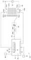
도 1은 일 실시 형태에 따른 플라즈마 처리 장치를 도시하는 도면이다.
도 2는 일 실시 형태에 따른 변압기를 도시하는 도면이다.
도 3은 실험에 사용한 플라즈마 처리 장치(10P)를 도시하는 도면이다.
도 4는 실험에 사용한 별도의 플라즈마 처리 장치(10R)를 도시하는 도면이다.
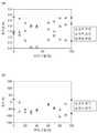
도 5의 (a)는, 플라즈마 처리 장치(10P)를 사용해서 구한, 분배 비율과 상부 전극(14), 하부 전극(16), 챔버 본체(12) 각각의 전류값과의 관계를 나타내는 그래프이며, 도 5의 (b)는, 플라즈마 처리 장치(10P)를 사용해서 구한, 분배 비율과 상부 전극(14), 하부 전극(16) 각각의 전위와의 관계를 나타내는 그래프이다.
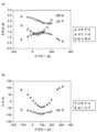
도 6의 (a)는, 플라즈마 처리 장치(10R)를 사용해서 구한, 하부 전극(16)의 리액턴스와 상부 전극(14), 하부 전극(16), 챔버 본체(12) 각각의 전류값과의 관계를 나타내는 그래프이며, 도 6의 (b)는, 플라즈마 처리 장치(10R)를 사용해서 구한, 하부 전극(16)의 리액턴스와 상부 전극(14), 하부 전극(16) 각각의 전위와의 관계를 나타내는 그래프이다.
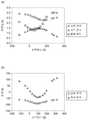
도 7의 (a)는, 플라즈마 처리 장치(10A)를 사용해서 구한, 분배 비율이 0%인 경우의 하부 전극(16)의 리액턴스와 상부 전극(14), 하부 전극(16), 챔버 본체(12) 각각의 전류값과의 관계를 나타내는 그래프이며, 도 7의 (b)는, 플라즈마 처리 장치(10A)를 사용해서 구한, 분배 비율이 0%인 경우의 하부 전극(16)의 리액턴스와 상부 전극(14), 하부 전극(16) 각각의 전위와의 관계를 나타내는 그래프이다.
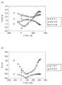
도 8의 (a)는, 플라즈마 처리 장치(10A)를 사용해서 구한, 분배 비율이 20%인 경우의 하부 전극(16)의 리액턴스와 상부 전극(14), 하부 전극(16), 챔버 본체(12) 각각의 전류값과의 관계를 나타내는 그래프이며, 도 8의 (b)는, 플라즈마 처리 장치(10A)를 사용해서 구한, 분배 비율이 20%인 경우의 하부 전극(16)의 리액턴스와 상부 전극(14), 하부 전극(16) 각각의 전위와의 관계를 나타내는 그래프이다.
도 9의 (a)는, 플라즈마 처리 장치(10A)를 사용해서 구한, 분배 비율이 40%인 경우의 하부 전극(16)의 리액턴스와 상부 전극(14), 하부 전극(16), 챔버 본체(12) 각각의 전류값과의 관계를 나타내는 그래프이며, 도 9의 (b)는, 플라즈마 처리 장치(10A)를 사용해서 구한, 분배 비율이 40%의 경우의 하부 전극(16)의 리액턴스와 상부 전극(14), 하부 전극(16) 각각의 전위와의 관계를 나타내는 그래프이다.
도 10의 (a)는, 플라즈마 처리 장치(10A)를 사용해서 구한, 분배 비율이 80%인 경우의 하부 전극(16)의 리액턴스와 상부 전극(14), 하부 전극(16), 챔버 본체(12) 각각의 전류값과의 관계를 나타내는 그래프이며, 도 10의 (b)는, 플라즈마 처리 장치(10A)를 사용해서 구한, 분배 비율이 80%인 경우의 하부 전극(16)의 리액턴스와 상부 전극(14), 하부 전극(16) 각각의 전위와의 관계를 나타내는 그래프이다.
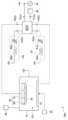
도 11은 다른 실시 형태에 따른 플라즈마 처리 장치를 도시하는 도면이다.
도 12는 도 11에 도시하는 플라즈마 처리 장치의 변압기를 일부 파단해서 도시하는 사시도이다.
도 13은 도 12에 나타내는 변압기의 3개 코일을 개략적으로 도시하는 도면이다.
도 14는 또 다른 실시 형태에 관한 플라즈마 처리 장치를 도시하는 도면이다.
도 15는 또 다른 실시 형태에 관한 플라즈마 처리 장치를 도시하는 도면이다.
도 16은 또 다른 실시 형태에 관한 플라즈마 처리 장치를 도시하는 도면이다.
도 17은 도 16에 나타내는 플라즈마 처리 장치의 변압기를 도시하는 도면이다.
도 18의 (a)는, 플라즈마 처리 장치(10E)를 사용해서 구한, 가변 콘덴서(50a)의 다이알 값과 챔버 본체(12), 상부 전극(14) 및 하부 전극(16) 각각의 전류와의 관계를 나타내는 그래프이며, 도 18의 (b)는, 플라즈마 처리 장치(10E)를 사용해서 구한, 가변 콘덴서(50a)의 다이알 값과 상부 전극(14) 및 하부 전극(16) 각각의 직류 전위를 나타내는 그래프이다.1 is a view showing a plasma processing apparatus according to one embodiment.
2 is a diagram showing a transformer according to one embodiment.
3 is a diagram showing a
4 is a view showing a separate
5A is a graph showing the relationship between the distribution ratio and the current value of each of the
6A shows the relationship between the reactance of the
7A is a graph showing the relationship between the reactance of the
8A is a graph showing the relationship between the reactance of the
9A is a graph showing the relationship between the reactance of the
10A shows the reactance of the
11 is a diagram showing a plasma processing apparatus according to another embodiment.
12 is a perspective view showing a part of the transformer of the plasma processing apparatus shown in Fig.
Fig. 13 is a view schematically showing three coils of the transformer shown in Fig. 12;
14 is a diagram showing a plasma processing apparatus according to still another embodiment.
15 is a diagram showing a plasma processing apparatus according to another embodiment.
16 is a diagram showing a plasma processing apparatus according to still another embodiment.
Fig. 17 is a view showing a transformer of the plasma processing apparatus shown in Fig. 16. Fig.
18A is a graph showing the relation between the dial value of the
이하, 도면을 참조하여 다양한 실시 형태에 대해서 상세하게 설명한다. 또한, 각 도면에서 동일하거나 또는 상당하는 부분에 대해서는 동일한 부호를 붙이기로 한다.Hereinafter, various embodiments will be described in detail with reference to the drawings. In the drawings, the same or equivalent parts are denoted by the same reference numerals.
도 1은, 일 실시 형태에 따른 플라즈마 처리 장치를 도시하는 도면이다. 도 1에 도시하는 플라즈마 처리 장치(10A)는, 용량 결합형 플라즈마 처리 장치이다. 플라즈마 처리 장치(10A)는, 챔버 본체(12), 제1 전극인 상부 전극(14), 제2 전극인 하부 전극(16), 고주파 전원(18), 정합기(38), 임피던스 조정 회로(50), 및 변압기(100A)를 구비하고 있다.1 is a view showing a plasma processing apparatus according to an embodiment. The
챔버 본체(12)는, 그 내부 공간을 챔버(12c)로서 제공하고 있다. 챔버 본체(12)는, 알루미늄과 같은 금속으로 형성되어 있다. 챔버 본체(12)의 내벽면에는 내플라즈마성의 피복이 형성되어 있다. 내플라즈마성의 피복은, 알루마이트 막, 산화이트륨 막과 같은 세라믹스제의 막일 수 있다. 챔버 본체(12)는, 대략 통 형상의 측벽부, 측벽부의 하단에 연속하는 저부, 및 측벽부의 상단에 연속하는 상단부를 갖고 있다. 챔버 본체(12)는, 접지되어 있다.The chamber
챔버 본체(12) 내에는, 스테이지(20)가 설치되어 있다. 스테이지(20)는, 하부 전극(16)을 포함하고 있다. 또한, 일 실시 형태에서는, 스테이지(20)는, 정전 척(22)을 더 포함하고 있다. 이 스테이지(20)는, 챔버 본체(12)의 저부로부터 연장되는 절연성의 지지체(24)에 의해 지지되어 있다. 하부 전극(16)은, 대략 원반 형상을 갖고 있으며, 알루미늄과 같은 도체로 형성되어 있다. 정전 척(22)은, 하부 전극(16) 상에 설치되어 있다. 정전 척(22)은, 유전체막 및 당해 유전체막 내에 내장된 전극을 포함하고 있다. 정전 척(22)의 전극에는 스위치를 통해서 전원이 접속되어 있다. 이 전원으로부터 정전 척(22)의 전극에 전압이 인가됨으로써, 정전 척(22)은 정전력을 발생한다. 정전 척(22)은, 당해 정전력에 의해, 그 위에 적재된 피가공물(W)을 흡착하여, 당해 피가공물(W)을 유지한다.In the
상부 전극(14)과 하부 전극(16)은, 챔버(12c) 내의 공간이 그들 사이에 개재하도록 설치되어 있다. 일 실시 형태에서는, 챔버 본체(12)의 상단부는, 개구되어 있다. 상부 전극(14)은, 절연성의 부재(26)를 개재해서 챔버 본체(12)의 상단부에 지지되어 있다. 상부 전극(14)은, 부재(26)와 함께, 챔버 본체(12)의 상단부의 개구를 폐쇄하고 있다. 상부 전극(14)은, 천장판(28) 및 지지체(30)를 포함하고 있다. 천장판(28)은 챔버(12c)에 면하고 있다. 이 천장판(28)은, 실리콘, 알루미늄 또는 석영과 같은 재료로 구성될 수 있다. 또한, 천장판(28)이 알루미늄으로 형성되어 있는 경우에는, 그 표면에는 내플라즈마성의 피복이 실시된다. 천장판(28)에는, 복수의 가스 토출 구멍(28a)이 형성되어 있다.The
지지체(30)는, 천장판(28)을 착탈 가능하게 지지하고 있다. 지지체(30)는, 예를 들어 알루미늄과 같은 도체로 형성되어 있다. 지지체(30)의 내부에는, 가스 확산 실(30a)이 형성되어 있다. 지지체(30)에는, 가스 확산 실(30a)과 복수의 가스 토출 구멍(28a)을 접속하는 복수의 구멍(30b)이 형성되어 있다. 또한, 가스 확산 실(30a)에는, 플라즈마 처리를 위한 가스를 공급하는 가스 공급부(32)가 접속되어 있다. 가스 공급부(32)는, 복수의 가스 소스, 매스 플로우 컨트롤러와 같은 복수의 유량 제어기, 및 복수의 밸브를 갖는다. 복수의 가스 소스 각각은, 복수의 유량 제어기 중 대응하는 유량 제어기, 및 복수의 밸브 중 대응하는 밸브를 통해서, 가스 확산 실(30a)에 접속되어 있다. 이 가스 공급부(32)는, 복수의 가스 소스 중 선택된 가스 소스로부터의 가스의 유량을 조정하여, 당해 가스를 가스 확산 실(30a)에 공급한다. 가스 확산 실(30a)에 공급된 가스는, 복수의 가스 토출 구멍(28a)으로부터 챔버(12c)에 공급된다.The
챔버 본체(12)의 측벽부에는, 피가공물의 반송을 위한 개구가 형성되어 있다. 이 개구는, 게이트 밸브(34)에 의해 개폐 가능하게 되어 있다. 또한, 챔버(12c)에는 배기 장치(36)가 접속되어 있다. 이 배기 장치(36)에 의해, 챔버(12c)의 압력이 감압된다.In the side wall portion of the
고주파 전원(18)은, 변압기(100A)의 일차 코일(101A)에 공급되는 고주파를 발생한다. 고주파 전원(18)은, 정합기(38)를 통해서 변압기(100A)의 일차 코일(101A)에 접속되어 있다. 정합기(38)는, 고주파 전원(18)의 출력 임피던스와 부하측의 임피던스를 정합시키기 위한 정합 회로를 갖고 있다.The high
변압기(100A)는, 일차 코일(101A), 제1 이차 코일(102A) 및 제2 이차 코일(103A)을 갖고 있다. 일차 코일(101A)의 일단은 단자(101a)이며, 타단은 단자(101b)이다. 단자(101a)는, 정합기(38)를 통해서 고주파 전원(18)에 접속되어 있다. 단자(101b)는, 접지를 통해서 고주파 전원(18)에 접속되어 있다.The
제1 이차 코일(102A) 및 제2 이차 코일(103A)은, 일차 코일(101A)에 전자 결합되어 있다. 제1 이차 코일(102A)의 일단은, 단자(102a)이다. 단자(102a)는, 상부 전극(14)에 전기적으로 접속되어 있다. 또한, 제2 이차 코일(103A)의 일단은, 단자(103a)이다. 단자(103a)는, 하부 전극(16)에 전기적으로 접속되어 있다.The first
변압기(100A)에서는, 제1 이차 코일(102A) 및 제2 이차 코일(103A)은, 단일한 코일로 형성된다. 구체적으로, 변압기(100A)의 이차측은 단일한 코일을 갖고 있고, 당해 단일 코일은 복수의 탭(100t)을 갖고 있다. 복수의 탭(100t)은, 선택적으로 접지에 접속되도록 구성되어 있다. 변압기(100A)에서는, 접지에 접속하도록 선택된 탭에 대하여 당해 단일 코일의 일방측이 제1 이차 코일(102A)이 되고, 타방측의 부분이 제2 이차 코일(103A)이 된다.In the
플라즈마 처리 장치(10A)에서는, 단자(103a)와 하부 전극(16)과의 사이의 직렬 회로에 임피던스 조정 회로(50)가 설치되어 있다. 임피던스 조정 회로(50)는, 가변 콘덴서 및/또는 인덕터를 가질 수 있다. 플라즈마 처리 장치(10A)에서는, 임피던스 조정 회로(50)는, 가변 콘덴서(50a) 및 인덕터(50b)를 갖는다. 가변 콘덴서(50a) 및 인덕터(50b)는, 하부 전극(16)과 단자(103a)와의 사이에서 직렬 접속되어 있다. 또한, 임피던스 조정 회로(50)는, 접지에 접속된 소자를 갖고 있지 않다.In the
일 실시 형태에서는, 변압기(100A)는, 도 2에 도시하는 구성을 가질 수 있다. 도 2는, 일 실시 형태에 따른 변압기를 도시하는 도면이다. 도 2에 도시하는 실시 형태에서는, 일차 코일(101A)의 권취선은, 중심 축선(CX)의 둘레에서 나선 형상으로 감겨 있다. 또한, 변압기(100A)는, 이차 코일로서 단일 코일(104)을 갖고 있고, 당해 단일 코일(104)은 복수의 탭(100t)을 갖고 있다. 일차 코일(101A)과 단일 코일(104)은 단면을 공유하도록 구성되어 있다. 예를 들어, 단일 코일(104)의 권취선은, 일차 코일(101A)의 권취선과, 중심 축선(CX)의 둘레에서, 교대로 또한 나선 형상으로 감겨 있다. 상술한 바와 같이, 복수의 탭(100t) 중 선택된 탭은 접지에 접속된다. 선택된 탭에 대하여 단일 코일(104)의 일방측의 부분은 제1 이차 코일(102A)이 되고, 타방측의 부분이 제2 이차 코일(103A)이 된다.In one embodiment, the
여기서, 변압기의 이차측의 출력 단자로부터 접지측을 본 회로의 리액턴스(X2)는, 다음 식 (1)과 같이 나타낼 수 있다. 식 (1)에서, L1은 일차 코일의 인덕턴스, L2는 이차 코일의 인덕턴스, Rm은 정합기의 레지스턴스, Xm은 정합기의 리액턴스, ω는 고주파의 각 주파수, k는 일차 코일과 이차 코일의 결합 계수이다.Here, the reactance (X2 ) of the circuit from the output terminal on the secondary side of the transformer to the ground side can be expressed by the following equation (1). In the equation (1), L1 is the inductance of the primary coil, L2 is the inductance of the secondary coil, Rm is the resistance of the matching device, Xm is the reactance of the matching device, It is the coupling coefficient of the secondary coil.
[수학식 1][Equation 1]

Rm 및 Xm은, 플라즈마 부하의 리액턴스 및 레지스턴스와 각각 동일 정도의 값이며, 리액턴스(L1ω)와 비교해서 충분히 작은 것이다. 따라서, 식 (1)은 다음 식 (2)에 나타내는 바와 같이 변형된다.Rm, and Xm are values approximately equal to the reactance and resistance of the plasma load, respectively, and sufficiently small compared with the reactance (L1ω ). Therefore, equation (1) is modified as shown in the following equation (2).
[수학식 2]&Quot; (2) "

k는 1에 가까운 값이므로, 식 (2)로부터 이해되는 바와 같이, 리액턴스(X2)는 상당히 작다. 또한, 도 2에 도시한 실시 형태의 변압기(100A)에서는, k는 대략 1이므로, 리액턴스(X2)는 대략 0이 된다. 따라서, 변압기(100A)와 임피던스 조정 회로(50)를 함께 사용해도, 임피던스 조정 회로(50)의 기능이 발휘된다. 그러므로, 플라즈마 처리 장치(10A)에 의하면, 변압기(100A)와 임피던스 조정 회로(50)에 의해, 하부 전극(16)의 전위를 정의 전위와 부의 전위와의 사이에서 크게 변화시키는 것이 가능하다. 그 결과, 플라즈마 처리 장치(10A)에서는, 하부 전극(16)의 위에 배치된 피가공물(W)에 입사하는 이온의 에너지의 조정 가능한 범위가 넓어진다.Since k is a value close to 1, the reactance (X2 ) is considerably small, as understood from the equation (2). Further, in the transformer (100A) of the embodiment shown in Figure 2, k because it is approximately 1, the reactance (X2) is approximately zero. Therefore, even if the
여기서, 몇 가지의 실험 결과에 대해서 설명한다. 먼저, 도 3에 도시한 바와 같이, 플라즈마 처리 장치(10A)로부터 임피던스 조정 회로(50)를 제거한 플라즈마 처리 장치(10P)를 준비하였다. 또한, 도 4에 도시한 바와 같이, 플라즈마 처리 장치(10A)로부터 변압기(100A)를 제거한 플라즈마 처리 장치(10R)를 준비하였다. 플라즈마 처리 장치(10P) 및 플라즈마 처리 장치(10R)의 양쪽에 있어서, 900sccm의 아르곤(Ar) 가스를 챔버(12c)에 공급하고, 챔버(12c)의 압력을 800mTorr(106.7Pa)로 설정하고, 고주파 전원(18)의 고주파의 주파수, 전력을 각각을 450kHz, 500W로 설정하였다. 플라즈마 처리 장치(10P)에서는, 다양한 분배 비율의 설정에 있어서, 분배 비율과 상부 전극(14), 하부 전극(16), 챔버 본체(12) 각각의 전류값과의 관계, 및 분배 비율과 상부 전극(14), 하부 전극(16) 각각의 전위와의 관계를 구하였다. 또한, 분배 비율은, 변압기(100A)의 이차측의 총 전력에 대하여 제2 이차 코일(103A)에 분배되는 전력의 비율(설정값)이다. 실험에서는, 복수의 탭(100t) 중 접지에 접속하는 탭을 변경함으로써 분배 비율을 설정하였다. 또한, 플라즈마 처리 장치(10R)에서는, 하부 전극(16)의 다양한 리액턴스의 설정에 있어서, 하부 전극(16)의 리액턴스와 상부 전극(14), 하부 전극(16), 챔버 본체(12) 각각의 전류값과의 관계, 및 하부 전극(16)의 리액턴스와 상부 전극(14), 하부 전극(16) 각각의 전위와의 관계를 구하였다. 또한, 임피던스 조정 회로(50)의 임피던스를 변경함으로써 하부 전극(16)의 리액턴스를 설정하였다.Here, some experimental results will be described. First, as shown in Fig. 3, a
도 5의 (a)에, 플라즈마 처리 장치(10P)를 사용해서 구한, 분배 비율과 상부 전극(14), 하부 전극(16), 챔버 본체(12) 각각의 전류값과의 관계를 나타내고, 도 5의 (b)에, 플라즈마 처리 장치(10P)를 사용해서 구한, 분배 비율과 상부 전극(14), 하부 전극(16) 각각의 전위와의 관계를 나타낸다. 또한, 도 6의 (a)에, 플라즈마 처리 장치(10R)를 사용해서 구한, 하부 전극(16)의 리액턴스와 상부 전극(14), 하부 전극(16), 챔버 본체(12) 각각의 전류값과의 관계를 나타내고, 도 6의 (b)에, 플라즈마 처리 장치(10R)를 사용해서 구한, 하부 전극(16)의 리액턴스와 상부 전극(14), 하부 전극(16) 각각의 전위와의 관계를 나타낸다.5A shows the relationship between the distribution ratio and the current value of each of the
도 5의 (a)에 도시한 바와 같이, 플라즈마 처리 장치(10P)에서는, 하부 전극(16)에 대한 전력의 분배 비율이 커지면, 하부 전극(16)에 유입하는 전류가 증대되었다. 하부 전극(16)에 유입하는 전류가 증대되면, 도 5의 (b)에 도시한 바와 같이, 하부 전극(16)의 전위가 부의 전위로 되었다. 또한, 하부 전극(16)의 전위가 부의 전위로 되어, 상부 전극(14)의 전위보다도 낮아지면, 하부 전극(16)을 향해서 이온이 가속되므로, 피가공물(W)에 입사하는 이온의 에너지가 높아진다.As shown in Fig. 5A, in the
또한, 도 6의 (a)에 도시한 바와 같이, 플라즈마 처리 장치(10R)에서는, 하부 전극(16)의 임피던스가 큰 경우에는, 상부 전극(14)으로부터 플라즈마에 유입된 전류의 대부분이 챔버 본체(12)로 흘렀다. 하부 전극(16)의 임피던스가 약 100Ω일 때, 플라즈마 시스의 임피던스가 상쇄되어, 하부 전극(16)에 흐르는 전류가 최대로 되었다. 도 6의 (a)와 도 6의 (b)를 모두 참조하면, 하부 전극(16)에 흐르는 전류가 증대되면, 하부 전극(16)의 전위는 낮아지고 있었다. 또한, 하부 전극(16)의 전위가 낮아지면, 하부 전극(16)을 향해서 이온이 가속되므로, 피가공물(W)에 입사하는 이온의 에너지가 높아진다.6 (a), in the
도 5의 (b)와 도 6의 (b)를 대비하면, 플라즈마 처리 장치(10P)에서는, 하부 전극(16)의 전위를 비교적 낮은 전위의 범위에서 조정하는 것이 가능하였다. 한편, 플라즈마 처리 장치(10R)에서는, 하부 전극(16)의 전위를 비교적 높은 전위의 범위에서 조정하는 것이 가능하였다. 즉, 변압기(100A)에 의하면, 피가공물(W)에 입사하는 이온의 에너지를 비교적 높은 에너지의 범위에서 조정하는 것이 가능한 것으로 확인되었다. 한편, 임피던스 조정 회로(50)에 의하면, 피가공물(W)에 입사하는 이온의 에너지를 비교적 낮은 에너지의 범위에서 조정하는 것이 가능한 것으로 확인되었다.5 (b) and 6 (b), it is possible to adjust the potential of the
또한, 플라즈마 처리 장치(10A)에 있어서, 900sccm의 아르곤(Ar) 가스를 챔버(12c)에 공급하고, 챔버(12c)의 압력을 800mTorr(106.7Pa)로 설정하고, 고주파 전원(18)의 고주파의 주파수, 전력을 각각을 450kHz, 500W로 설정하였다. 그리고, 다양한 분배 비율 및 다양한 하부 전극(16)의 리액턴스의 설정에 있어서, 상부 전극(14), 하부 전극(16), 챔버 본체(12) 각각의 전류값, 및 상부 전극(14), 하부 전극(16) 각각의 전위와의 관계를 구하였다.In the
도 7의 (a)에, 플라즈마 처리 장치(10A)를 사용해서 구한, 분배 비율이 0%인 경우의 하부 전극(16)의 리액턴스와 상부 전극(14), 하부 전극(16), 챔버 본체(12) 각각의 전류값과의 관계를 나타내고, 도 7의 (b)에, 플라즈마 처리 장치(10A)를 사용해서 구한, 분배 비율이 0%인 경우의 하부 전극(16)의 리액턴스와 상부 전극(14), 하부 전극(16) 각각의 전위와의 관계를 나타낸다. 도 8의 (a)에, 플라즈마 처리 장치(10A)를 사용해서 구한, 분배 비율이 20%인 경우의 하부 전극(16)의 리액턴스와 상부 전극(14), 하부 전극(16), 챔버 본체(12) 각각의 전류값과의 관계를 나타내고, 도 8의 (b)에, 플라즈마 처리 장치(10A)를 사용해서 구한, 분배 비율이 20%인 경우의 하부 전극(16)의 리액턴스와 상부 전극(14), 하부 전극(16) 각각의 전위와의 관계를 나타낸다. 도 9의 (a)에, 플라즈마 처리 장치(10A)를 사용해서 구한, 분배 비율이 40%인 경우의 하부 전극(16)의 리액턴스와 상부 전극(14), 하부 전극(16), 챔버 본체(12) 각각의 전류값과의 관계를 나타내고, 도 9의 (b)에, 플라즈마 처리 장치(10A)를 사용해서 구한, 분배 비율이 40%인 경우의 하부 전극(16)의 리액턴스와 상부 전극(14), 하부 전극(16) 각각의 전위와의 관계를 나타낸다. 도 10의 (a)에, 플라즈마 처리 장치(10A)를 사용해서 구한, 분배 비율이 80%인 경우의 하부 전극(16)의 리액턴스와 상부 전극(14), 하부 전극(16), 챔버 본체(12) 각각의 전류값과의 관계를 나타내고, 도 10의 (b)에, 플라즈마 처리 장치(10A)를 사용해서 구한, 분배 비율이 80%인 경우의 하부 전극(16)의 리액턴스와 상부 전극(14), 하부 전극(16) 각각의 전위와의 관계를 나타낸다. 또한, 분배 비율이 0%인 경우에는, 플라즈마 처리 장치(10R)와 동등한 환경이므로, 도 6의 (a)와 도 7의 (a)는 동일하고, 도 6의 (b)와 도 7의 (b)는 동일하게 되어 있다.7A shows the reactance of the
도 7의 (a), 도 8의 (a), 도 9의 (a) 및 도 10의 (a)에 도시한 바와 같이, 플라즈마 처리 장치(10A)에서도, 분배 비율이 커짐에 따라서, 하부 전극(16)에 흐르는 전류가 증대되었다. 또한, 도 7의 (b), 도 8의 (b), 도 9의 (b) 및 도 10의 (b)에 도시한 바와 같이, 분배 비율이 커짐에 따라서, 하부 전극(16)의 전위가 낮아지고 있었다. 또한, 분배 비율이 커짐에 따라서, 하부 전극(16)의 전위가 상부 전극(14)의 전위보다도 낮아지고 있었다. 따라서, 플라즈마 처리 장치(10A)에 의하면, 변압기(100A)에 의한 전력의 분배에 의해, 비교적 높은 에너지의 범위에서 피가공물(W)에 입사하는 이온의 에너지를 조정하는 것이 가능한 것으로 확인되었다. 또한, 도 7의 (b) 및 도 8의 (b)에 도시한 바와 같이, 하부 전극(16)의 임피던스 조정에 의해, 하부 전극(16)의 전위를 비교적 높은 전위의 범위에서 조정하는 것이 가능한 것으로 확인되었다. 따라서, 플라즈마 처리 장치(10A)에 의하면, 임피던스 조정 회로(50)의 임피던스의 조정에 의해, 비교적 낮은 에너지의 범위에서 피가공물(W)에 입사하는 이온의 에너지를 조정하는 것이 가능한 것으로 확인되었다. 그러므로, 플라즈마 처리 장치(10A)에 의하면, 하부 전극(16)의 위에 배치된 피가공물(W)에 입사하는 이온의 에너지의 조정 가능한 범위가 넓어진다.As shown in FIG. 7A, FIG. 8A, FIG. 9A and FIG. 10A, in the
이어서, 도 11을 참조하여, 다른 실시 형태에 따른 플라즈마 처리 장치에 대해서 설명한다. 도 11은, 다른 실시 형태에 따른 플라즈마 처리 장치를 도시하는 도면이다. 이하, 도 11에 도시하는 플라즈마 처리 장치(10B)가 플라즈마 처리 장치(10A)와 상이한 점에 대해서 설명하고, 중복되는 설명을 생략한다.Next, a plasma processing apparatus according to another embodiment will be described with reference to FIG. 11 is a diagram showing a plasma processing apparatus according to another embodiment. Hereinafter, the
플라즈마 처리 장치(10B)는, 변압기(100A)가 아니라, 변압기(100B)를 구비하고 있다. 또한, 플라즈마 처리 장치(10B)는, 추가의 임피던스 조정 회로(51)를 더 구비하고 있다. 임피던스 조정 회로(51)는, 가변 콘덴서 및/또는 인덕터를 가질 수 있다. 플라즈마 처리 장치(10B)에서는, 임피던스 조정 회로(51)는, 가변 콘덴서(51a) 및 인덕터(51b)를 갖는다. 가변 콘덴서(51a) 및 인덕터(51b)는, 상부 전극(14)과 변압기(100B)의 단자(102a)와의 사이에서 직렬 접속되어 있다. 또한, 임피던스 조정 회로(51)는, 접지에 접속된 소자를 갖고 있지 않다. 고주파 전원(18)은, 정합기(38)를 통해서 변압기(100B)의 단자(101a)에 접속되어 있다. 임피던스 조정 회로(50)는, 하부 전극(16)과 변압기(100B)의 단자(103a)와의 사이에서 접속되어 있다. 변압기(100B)의 단자(102b)와 단자(103b)는 접지에 접속되어 있다.The
도 12는, 도 11에 도시하는 플라즈마 처리 장치(10B)의 변압기(100B)를 일부 파단해서 도시하는 사시도이다. 도 13은, 도 12에 나타내는 변압기(100B)의 3개의 코일을 개략적으로 도시하는 도면이다. 도 12 및 도 13에 나타내는 변압기(100B)는, 회전축(112), 일차 코일(101B), 제1 이차 코일(102B) 및 제2 이차 코일(103B)을 구비하고 있다. 제1 이차 코일(102B) 및 제2 이차 코일(103B)은, 이차측 코일 쌍(106)을 구성하고 있다. 일 실시 형태에서, 변압기(100B)는, 지지 부재(122, 124), 지주(126), 지지 부재(128, 130), 지지 부재(132, 134), 단자(101a, 101b), 단자(102a, 102b) 및 단자(103a, 103b)를 더 구비하고 있다.12 is a perspective view showing a part of the
회전축(112)은, 대략 원기둥 형상을 이루고 있다. 회전축(112)은, 그 중심 축선(RX) 둘레로, 즉, 중심 축선(RX)을 회전 축선으로 해서, 회전 가능하게 설치되어 있다. 일 실시 형태에서는, 회전축(112)은, 지지 부재(122)와 지지 부재(124)에 의해 회전 가능하게 지지되어 있다. 지지 부재(122) 및 지지 부재(124)는, 판상의 부재이며, 대략 사각형의 평면 형상을 갖는다. 지지 부재(122) 및 지지 부재(124)는, 절연체로 형성되어 있다. 지지 부재(122) 및 지지 부재(124)는, 중심 축선(RX)에 교차 또는 대략 직교하도록 설치되어 있고, 그들의 판 두께 방향이 중심 축선(RX)이 연장되는 방향(RD)에 대략 일치하도록, 방향(RD)을 따라 배열되어 있다. 지지 부재(122)의 코너부에는 지주(126)의 일단이 고정되어 있고, 지지 부재(124)의 코너부에는 지주(126)의 타단이 고정되어 있다. 회전축(112)의 일단부는, 지지 부재(122)를 관통하여, 지지 부재(122)로부터 돌출되어 있다. 이 회전축(112)의 일단부는, 구동 기구(예를 들어, 모터)에 접속되어 있다.The
지지 부재(128) 및 지지 부재(130)는, 대략 원반 형상의 부재이며, 절연체로 형성되어 있다. 지지 부재(128) 및 지지 부재(130)는, 지지 부재(122)와 지지 부재(124)와의 사이에서 중심 축선(RX)에 교차 또는 대략 직교하도록 설치되어 있고, 그들의 판 두께 방향이 방향(RD)에 대략 일치하도록 방향(RD)을 따라 배열되어 있다. 또한, 지지 부재(132) 및 지지 부재(134)는, 대략 원반 형상의 부재이며, 절연체로 형성되어 있다. 지지 부재(132) 및 지지 부재(134)는, 지지 부재(128)와 지지 부재(130)와의 사이에서 중심 축선(RX)에 교차 또는 대략 직교하도록 설치되어 있고, 그들의 판 두께 방향이 방향(RD)에 대략 일치하도록 방향(RD)을 따라 배열되어 있다. 회전축(112)은, 지지 부재(128, 130, 132, 134) 각각의 중심을 관통하고 있다. 지지 부재(128, 130, 132, 134)는, 회전축(112)에 고정되어 있다.The
일차 코일(101B)은, 중심 축선(RX)에 직교하는 제1 축선(AX1) 둘레에 연장되어 있다. 일 실시 형태에서는, 제1 축선(AX1)은, 지지 부재(122)와 지지 부재(124)와의 중간에서 중심 축선(RX)에 직교하고 있다. 일차 코일(101B)은, 지지 부재(122)의 외측과 지지 부재(124)의 외측을 교대로 지나도록, 제1 축선(AX1) 중심에 감겨 있다.The
일차 코일(101B)의 일단은, 단자(101a)에 접속되어 있다. 일 실시 형태에서는, 단자(101a)는, 지지 부재(122)의 일면(122a)(변압기(100B)의 외측을 향한 면)에 설치되어 있다. 또한, 일차 코일(101B)의 타단은, 단자(101b)에 접속되어 있다. 일 실시 형태에서는, 단자(101b)는, 지지 부재(124)의 일면(124a)(변압기(100B)의 외측을 향한 면)에 설치되어 있다.One end of the
제1 이차 코일(102B)은, 제2 축선(AX2) 둘레에 연장되어 있다. 제2 축선(AX2)은, 일차 코일(101B)에 의해 둘러싸인 영역 내에서 중심 축선(RX)에 직교하고 있다. 일 실시 형태에서는, 제2 축선(AX2)은, 지지 부재(128)와 지지 부재(130)와의 중간에서 중심 축선(RX)에 직교하고 있다. 제1 이차 코일(102B)은, 지지 부재(128)의 외측과 지지 부재(130)의 외측을 교대로 지나도록, 제2 축선(AX2) 중심에 감겨 있다. 제1 이차 코일(102B)은, 지지 부재(128) 및 지지 부재(130)를 개재해서 회전축(112)에 의해 지지되어 있다.The first
제1 이차 코일(102B)의 일단은, 단자(102a)에 접속되어 있다. 또한, 제1 이차 코일(102B)의 타단은, 단자(102b)에 접속되어 있다. 일 실시 형태에서는, 단자(102a) 및 단자(102b)는, 지지 부재(122)의 일면(122a)에 설치되어 있다. 회전축(112)은, 동축 형상으로 설치된 제1 도체와 제2 도체를 포함하고 있고, 제1 이차 코일(102B)의 일단은 제1 도체에 접속되어 있고, 제1 이차 코일(102B)의 타단은 제2 도체에 접속되어 있다. 제1 도체는, 로터리 커넥터(140) 내의 슬립 링을 통해서 단자(102a)에 접속되어 있다. 또한, 제2 도체는, 로터리 커넥터(140) 내의 다른 슬립 링을 통해서 단자(102b)에 접속되어 있다.One end of the first
제2 이차 코일(103B)은, 제3 축선(AX3) 둘레에 연장되어 있다. 제3 축선(AX3)은, 일차 코일(101B)에 의해 둘러싸인 영역 내에서 중심 축선(RX)에 직교하고 있다. 또한, 제3 축선(AX3)은, 제2 축선(AX2)에 교차하고 있다. 제3 축선(AX3)과 제2 축선(AX2)은, 서로의 사이에 소정의 각도(θp)를 이루고 있다. 각도(θp)는, 한정되는 것은 아니지만, 예를 들어 90도이다. 일 실시 형태에서는, 제3 축선(AX3)은, 지지 부재(132)와 지지 부재(134)와의 중간에서 중심 축선(RX)에 직교하고 있다. 제2 이차 코일(103B)은, 지지 부재(132)의 외측과 지지 부재(134)의 외측을 교대로 지나도록, 제3 축선(AX3) 중심에 감겨 있다. 제2 이차 코일(103B)은, 지지 부재(132) 및 지지 부재(134)를 개재해서 회전축(112)에 의해 지지되어 있다. 이 제2 이차 코일(103B)과 제1 이차 코일(102B)과의 사이에는, 절연 거리가 확보되어 있다.The second
제2 이차 코일(103B)의 일단은, 단자(103a)에 접속되어 있다. 또한, 제2 이차 코일(103B)의 타단은, 단자(103b)에 접속되어 있다. 일 실시 형태에서는, 단자(103a) 및 단자(103b)는, 지지 부재(124)의 일면(124a)에 설치되어 있다. 회전축(112)은, 동축 형상으로 설치된 제3 도체와 제4 도체를 포함하고 있고, 제2 이차 코일(103B)의 일단은 제3 도체에 접속되어 있고, 제2 이차 코일(103B)의 타단은 제4 도체에 접속되어 있다. 제3 도체는, 지지 부재(124)의 근방에 설치된 별도의 로터리 커넥터의 슬립 링을 통해서 단자(103a)에 접속되어 있다. 또한, 제4 도체는, 당해 별도의 로터리 커넥터 내의 다른 슬립 링을 통해서 단자(103b)에 접속되어 있다.One end of the second
변압기(100B)에서는, 일차 코일(101B)에 고주파 전원(18)으로부터의 고주파가 공급되면, 일차 코일(101B)이 제1 축선(AX1)이 연장되는 방향에 대략 평행한 방향으로 자속이 발생한다. 또한, 이차측 코일 쌍(106)의 회전 각도를 조정함으로써, 제1 이차 코일(102B)을 관통하는 자속의 양, 및 제2 이차 코일(103B)을 관통하는 자속의 양이 변화한다. 제1 이차 코일(102B)에는, 그것을 관통하는 자속의 양에 따른 유도 기전력이 발생한다. 또한, 제2 이차 코일(103B)에는, 그것을 관통하는 자속의 양에 따른 유도 기전력이 발생한다. 따라서, 변압기(100B)에 의하면, 제1 이차 코일(102B)에 분배되는 고주파의 전력과 제2 이차 코일(103B)에 분배되는 고주파의 전력의 비가 조정될 수 있다. 이러한 변압기(100B)를 갖는 플라즈마 처리 장치(10B)에 의하면, 플라즈마 처리 장치(10A)와 마찬가지로, 하부 전극(16)의 위에 배치된 피가공물(W)에 입사하는 이온의 에너지의 조정 가능한 범위가 넓어진다.In the
이어서, 도 14를 참조하여, 또 다른 실시 형태에 관한 플라즈마 처리 장치에 대해서 설명한다. 도 14는, 또 다른 실시 형태에 관한 플라즈마 처리 장치를 도시하는 도면이다. 이하, 도 14에 도시하는 플라즈마 처리 장치(10C)가 플라즈마 처리 장치(10A)와 상이한 점에 대해서 설명하고, 중복되는 설명을 생략한다.Next, a plasma processing apparatus according to still another embodiment will be described with reference to Fig. 14 is a diagram showing a plasma processing apparatus according to still another embodiment. The
플라즈마 처리 장치(10C)에서는, 임피던스 조정 회로(50)가, 복수의 탭(100t)과 접지와의 사이에서 접속되어 있다. 이와 같이, 임피던스 조정 회로(50)는, 하부 전극(16)과 변압기(100A)의 이차측의 코일이 접속되는 접지와의 사이의 직렬 회로에 설치될 수 있다.In the
이어서, 도 15를 참조하여, 또 다른 실시 형태에 관한 플라즈마 처리 장치에 대해서 설명한다. 도 15는, 또 다른 실시 형태에 관한 플라즈마 처리 장치를 도시하는 도면이다. 이하, 도 15에 도시하는 플라즈마 처리 장치(10D)가 플라즈마 처리 장치(10B)와 상이한 점에 대해서 설명하고, 중복되는 설명을 생략한다.Next, a plasma processing apparatus according to still another embodiment will be described with reference to Fig. 15 is a diagram showing a plasma processing apparatus according to still another embodiment. Hereinafter, the
플라즈마 처리 장치(10D)에서는, 임피던스 조정 회로(50)가 단자(103b)와 접지와의 사이에서 접속되어 있다. 또한, 임피던스 조정 회로(51)가 단자(102b)와 다른 접지와의 사이에서 접속되어 있다. 이와 같이, 제1 이차 코일(102B)과 제2 이차 코일(103B)이 별개의 접지에 접속되어 있는 경우에는, 제1 이차 코일(102B)과 접지와의 사이, 및 제2 이차 코일(103B)과 접지와의 사이에, 개별로 임피던스 조정 회로가 설치되어도 된다.In the
이어서, 도 16 및 도 17을 참조하여, 또 다른 실시 형태에 관한 플라즈마 처리 장치에 대해서 설명한다. 도 16은, 또 다른 실시 형태에 관한 플라즈마 처리 장치를 도시하는 도면이다. 도 17은, 도 16에 나타내는 플라즈마 처리 장치의 변압기를 도시하는 도면이다. 이하, 도 16에 나타내는 플라즈마 처리 장치(10E)가 플라즈마 처리 장치(10A)와 상이한 점에 대해서 설명하고, 중복되는 설명을 생략한다.Next, a plasma processing apparatus according to still another embodiment will be described with reference to Figs. 16 and 17. Fig. 16 is a diagram showing a plasma processing apparatus according to still another embodiment. Fig. 17 is a view showing a transformer of the plasma processing apparatus shown in Fig. 16. Fig. Hereinafter, the point that the
플라즈마 처리 장치(10E)는, 변압기(100A)가 아니라, 변압기(100E)를 구비하고 있다. 변압기(100E)는, 일차 코일(101E), 제1 이차 코일(102E) 및 제2 이차 코일(103E)을 구비하고 있다. 일차 코일(101E)은, 일차 코일(101A)과 마찬가지의 코일이다. 일차 코일(101E)의 일단은 단자(101a)이며, 정합기(38)를 통해서 고주파 전원(18)에 접속되어 있다. 일차 코일(101E)의 타단은 단자(101b)이며, 고주파 전원(18)에 접속되어 있고, 접지되어 있다.The
제1 이차 코일(102E) 및 제2 이차 코일(103E)은, 제1 이차 코일(102A) 및 제2 이차 코일(103A)과 마찬가지로, 단일 코일로 형성되어 있다. 이 단일 코일의 중간 노드(101n)는 단자(101e)에 접속되어 있다. 단자(101e)는 접지에 접속되어 있다. 노드(101n)에 대하여 단일 코일의 일방측 부분은 제1 이차 코일(102E)이며, 노드(101n)에 대하여 단일 코일의 타방측 부분은 제2 이차 코일(103E)이다. 제1 이차 코일(102E)의 일단은 단자(102a)이며, 임피던스 조정 회로(50)를 통해서 상부 전극(14)에 접속되어 있다. 또한, 제2 이차 코일(103E)의 일단은 단자(103a)이며, 콘덴서(60)를 통해서 하부 전극(16)에 접속되어 있다. 이 변압기(100E)에서는, 단일 코일의 권취선에 있어서 접지되는 개소가 고정되어 있다. 따라서, 제1 이차 코일(102E)의 권취수와 제2 이차 코일(103E)의 권취수의 비는 일정하다.The first
여기서, 일차 코일에 고주파 전원이 접속되고, 이차 코일에 복소 임피던스(Z2)의 부하가 접속되어 있는 경우에는, 일차 코일의 전류값과 이차 코일의 전류값과의 비는, 이하의 식 (3)으로 표현된다. 식 (3)에서, L1은 일차 코일의 자기 인덕턴스, L2는 이차 코일의 자기 인덕턴스, k는 일차 코일과 이차 코일의 사이의 결합 계수, ω는 고주파의 각 주파수이다. 또한, 복소 임피던스(Z2)는, 플라즈마의 임피던스와 이차 코일과 플라즈마와의 사이의 급전 회로의 임피던스이다.Here, when a high frequency power source is connected to the primary coil and a load of a complex impedance (Z2 ) is connected to the secondary coil, the ratio of the current value of the primary coil to the current value of the secondary coil is expressed by the following equation ). In equation (3), L1 is the magnetic inductance of the primary coil, L2 is the magnetic inductance of the secondary coil, k is the coupling coefficient between the primary and secondary coils, and ω is the angular frequency of the high frequency. The complex impedance (Z2 ) is the impedance of the plasma and the impedance of the power supply circuit between the secondary coil and the plasma.
[수학식 3]&Quot; (3) "

식 (3)의 분모가 작아지도록, 즉, 이차측에서 직렬 공진이 발생하도록 복소 임피던스(Z2)를 조정하면, 이차측으로 흘러드는 전류의 값이 커진다. 한편, 식 (3)의 분모가 커지도록 복소 임피던스(Z2)를 조정하면, 이차측으로 흘러드는 전류의 값이 작아진다. 변압기(100E)에서는, 2개의 이차 코일 중 한쪽의 이차 코일에 흐르는 전류가 커지고, 한쪽의 이차 코일에 분배되는 고주파의 전력이 증대되면, 다른 쪽의 이차 코일에 분배되는 고주파의 전력은 작아진다. 따라서, 2개의 이차 코일을 구성하는 단일 코일의 접지 개소가 고정되어 있어도, 임피던스 조정 회로(50)에 의한 임피던스의 조정에 의해, 상부 전극(14)에 공급되는 고주파의 전력과 하부 전극(16)에 공급되는 고주파의 전력을 조정하는 것이 가능하다. 그러므로, 플라즈마 처리 장치(10E)에 의하면, 하부 전극(16)에 입사하는 이온의 에너지를 조정하는 것이 가능하다.The denominator of the equation 3 is reduced, that is, by adjusting the complex impedance (Z2) so that the series resonance occurs at the secondary side, the larger the value of a current flowing the secondary side. On the other hand, if the complex impedance Z2 is adjusted so that the denominator of equation (3) becomes larger, the value of the current flowing to the secondary side becomes smaller. In the
이하, 플라즈마 처리 장치(10E)의 평가를 위해서 행한 실험의 결과에 대해 설명한다. 이 실험에 사용한 변압기(100E)의 일차 코일(101E)은, 직경이 42mm, 권취수가 27인 코일이었다. 또한, 제1 이차 코일(102E) 및 제2 이차 코일(103E)을 구성하는 단일 코일도, 직경 42mm, 권취수 27의 코일이었다. 이 단일 코일은 13턴째를 접지에 접속하였다. 그리고, 600sccm의 아르곤(Ar) 가스를 챔버(12c)에 공급하고, 챔버(12c)의 압력을 800mTorr(106.7Pa)로 설정하고, 고주파 전원(18)의 고주파의 주파수, 전력을 각각 13.56MHz, 200W로 설정하였다. 또한, 임피던스 조정 회로(50)의 가변 콘덴서(50a)의 다이알 값을 변경하여, 임피던스 조정 회로(50)의 임피던스를 다양한 임피던스로 설정하면서, 챔버 본체(12), 상부 전극(14) 및 하부 전극(16) 각각의 전류, 상부 전극(14) 및 하부 전극(16) 각각의 고주파 전압, 및 상부 전극(14) 및 하부 전극(16) 각각의 직류 전위를 측정하였다.Hereinafter, the results of the experiments performed for the evaluation of the
도 18의 (a)에, 가변 콘덴서(50a)의 다이알 값과 챔버 본체(12), 상부 전극(14) 및 하부 전극(16) 각각의 전류와의 관계를 나타내고, 도 18의 (b)에, 가변 콘덴서(50a)의 다이알 값과 상부 전극(14) 및 하부 전극(16) 각각의 직류 전위와의 관계를 나타낸다.18A shows the relationship between the dial value of the
실험에 사용한 임피던스 조정 회로(50)에서는, 가변 콘덴서(50a)의 다이알 값이 8 근방일 때, 제1 이차 코일(102E)의 임피던스, 임피던스 조정 회로(50)의 임피던스, 및 상부 전극(14)의 플라즈마 부하의 임피던스가 직렬 공진 상태로 되었다. 즉, 식 (3)에 나타낸 분모가 제로인 상태가 되었다. 이 직렬 공진 상태에서는, 상부 전극(14)에만 전류가 흐르고 있고, 하부 전극(16)에는 전류가 거의 흐르고 있지 않았다. 가변 콘덴서(50a)의 다이알 값이 8보다 작은 상태에서는, 식 (3)의 분모는 양으로 되고, 가변 콘덴서(50a)의 다이알 값이 8보다 큰 상태에서는, 식 (3)의 분모는 음으로 된다. 따라서, 상부 전극(14)으로부터 하부 전극(16)으로 흐르는 전류의 방향을 동위상의 방향으로 하면, 가변 콘덴서(50a)의 다이알 값이 8보다 작은 상태에서는 역위상의 전류가 흐르고, 가변 콘덴서(50a)의 다이알 값이 8보다 큰 상태에서는 동위상의 전류가 흐르고 있었다. 이와 같이, 임피던스 조정 회로(50)에 의해, 상부 전극(14)과 하부 전극(16)에 공급되는 전력비를 조정하는 것이 가능하다고 할 수 있다.The impedance of the first
도 18의 (a)에 도시한 바와 같이, 가변 콘덴서(50a)의 다이알 값을 8보다도 더 큰 값으로 설정한 결과, 상부 전극(14)의 전류값이 감소하고, 하부 전극(16)의 전류값이 증대되었다. 또한, 가변 콘덴서(50a)의 다이알 값이 8보다도 큰 어떤 값일 때, 상부 전극(14)의 전류값과 하부 전극(16)의 전류값이 대략 동일해지고, 챔버 본체(12)에 흐르는 전류가 최소로 되었다. 따라서, 가변 콘덴서(50a)의 다이알 값이 이러한 값으로 설정되었을 때는, 플라즈마가 상부 전극(14)과 하부 전극(16)과의 사이에 갇혀 있게 된다. 그러므로, 가변 콘덴서(50a)의 조정에 의해, 플라즈마를 안정되게 생성하는 것이 가능한 것으로 확인되었다.18A, when the dial value of the
또한, 도 18의 (b)에 도시한 바와 같이, 가변 콘덴서(50a)의 다이알 값에 따라, 하부 전극(16)의 직류 전위는, 음의 전위로부터 양의 전위까지 크게 변화하였다. 따라서, 플라즈마 처리 장치(10E)에서는, 하부 전극(16)의 위에 배치된 피가공물에 입사하는 이온의 에너지의 조정 가능한 범위가 넓은 것으로 확인되었다.18 (b), the dc potential of the
이상, 다양한 실시 형태에 대해서 설명해 왔지만, 상술한 실시 형태에 한정되지 않고 다양한 변형 형태를 구성할 수 있다. 예를 들어, 임피던스 조정 회로가 배치되는 개소는, 상술한 실시 형태에서 당해 임피던스 조정 회로가 배치된 개소에 한정되는 것은 아니다. 임피던스 조정 회로는, 상부 전극(14)과 제1 이차 코일의 타단에 접속된 접지와의 사이의 직렬 회로, 및 하부 전극(16)과 제2 이차 코일의 타단에 접속된 접지와의 사이의 직렬 회로 중 한쪽 또는 양쪽에 있어서 적소에 설치하는 것이 가능하다.Various embodiments have been described above, but the present invention is not limited to the above-described embodiments, and various modifications can be made. For example, the portion where the impedance adjusting circuit is disposed is not limited to the portion where the impedance adjusting circuit is disposed in the above-described embodiment. The impedance adjusting circuit includes a series circuit between the
10A, 10B, 10C, 10D, 10E : 플라즈마 처리 장치
12 : 챔버 본체12c : 챔버
14 : 상부 전극16 : 하부 전극
18 : 고주파 전원20 : 스테이지
32 : 가스 공급부36 : 배기 장치
38 : 정합기50, 51 : 임피던스 조정 회로
100A, 100B, 100E : 변압기101A, 101B, 101E : 일차 코일
102A, 102B, 102E : 제1 이차 코일103A, 103B, 103E : 제2 이차 코일10A, 10B, 10C, 10D, 10E: Plasma processing apparatus
12:
14: upper electrode 16: lower electrode
18: high-frequency power source 20: stage
32: gas supply part 36: exhaust device
38: Matching
100A, 100B, 100E:
102A, 102B, 102E: first
Claims (9)
Translated fromKorean챔버를 제공하는 챔버 본체와,
상기 챔버 내의 공간이 그들 사이에 개재하도록 설치된 제1 전극 및 제2의 전극과,
고주파 전원과,
상기 고주파 전원에 접속된 임피던스 정합용 정합기와,
상기 고주파 전원에 상기 정합기를 통해서 접속된 일차 코일, 및 제1 이차 코일 및 제2 이차 코일을 포함하는 변압기이며, 상기 제1 이차 코일의 일단은 상기 제1 전극에 접속되어 있고, 상기 제2 이차 코일의 일단은 상기 제2 전극에 접속된, 상기 변압기와,
가변의 임피던스를 갖고, 상기 제1 전극과 상기 제1 이차 코일의 타단에 접속된 접지와의 사이의 제1 직렬 회로, 및 상기 제2 전극과 상기 제2 이차 코일의 타단에 접속된 접지와의 사이의 제2 직렬 회로 중 적어도 한쪽에 설치된 적어도 하나의 임피던스 조정 회로를 포함하고,
상기 적어도 하나의 임피던스 조정 회로는, 접지에 접속된 소자를 포함하고 있지 않은, 플라즈마 처리 장치.A capacitively coupled plasma processing apparatus comprising:
A chamber body for providing a chamber,
A first electrode and a second electrode provided so that a space in the chamber is interposed therebetween,
A high-
An impedance matching matching circuit connected to the high frequency power source,
A primary coil connected to the high frequency power source through the matching device, and a first secondary coil and a second secondary coil, one end of the first secondary coil being connected to the first electrode, One end of the coil is connected to the second electrode, the transformer,
A first series circuit between the first electrode and a ground connected to the other end of the first secondary coil and a second series circuit between the first electrode and the ground connected to the other end of the second secondary coil, And at least one impedance adjusting circuit provided in at least one of the second series circuits between the first and second series circuits,
Wherein the at least one impedance adjusting circuit does not include an element connected to a ground.
상기 일차 코일, 상기 제1 이차 코일, 및 상기 제2 이차 코일은, 동축으로 설치되어 있고,
상기 제1 이차 코일의 권취선은, 상기 제1 이차 코일과 상기 일차 코일이 단면을 공유하도록, 상기 일차 코일의 중심 축선의 둘레에서 감겨 있고,
상기 제2 이차 코일의 권취선은, 상기 제2 이차 코일과 상기 일차 코일이 단면을 공유하도록, 상기 중심 축선의 둘레에서 감겨 있고,
상기 제1 이차 코일 및 상기 제2 이차 코일은, 접지에 선택적으로 접속 가능한 복수의 탭을 포함하는 단일 코일로 형성되는, 플라즈마 처리 장치.The method according to claim 1,
Wherein the primary coil, the first secondary coil, and the second secondary coil are coaxial,
Wherein the winding wire of the first secondary coil is wound around the central axis of the primary coil so that the first secondary coil and the primary coil share a cross section,
The winding wire of the second secondary coil is wound around the central axis so that the second secondary coil and the primary coil share a cross section,
Wherein the first secondary coil and the second secondary coil are formed of a single coil including a plurality of taps selectively connectable to ground.
상기 변압기는, 그 중심 축선을 회전 축선으로 해서 회전 가능한 회전축을 더 포함하고,
상기 일차 코일은, 상기 중심 축선에 직교하는 제1 축선의 둘레에서 연장되고,
상기 제1 이차 코일은, 제2 축선의 둘레에서 연장되고, 상기 회전축에 의해 지지되어 있고, 상기 제2 축선은 상기 일차 코일에 의해 둘러싸인 영역 내에서 상기 중심 축선에 직교하고 있고,
상기 제2 이차 코일은, 제3 축선 둘레에 연장되고, 상기 회전축에 의해 지지되어 있고, 상기 제3 축선은, 상기 영역 내에서 상기 중심 축선에 직교하고 또한 상기 제2 축선과 소정의 각도를 이루고 있는, 플라즈마 처리 장치.The method according to claim 1,
Wherein the transformer further includes a rotation shaft rotatable about a central axis of the transformer as a rotation axis,
Wherein the primary coil extends around a first axis orthogonal to the central axis,
Wherein the first secondary coil extends around a second axis and is supported by the rotation axis and the second axis is orthogonal to the central axis in an area surrounded by the primary coil,
Wherein the second secondary coil extends around a third axis and is supported by the rotation axis and the third axis is perpendicular to the central axis within the region and at a predetermined angle with the second axis Gt;
상기 일차 코일, 상기 제1 이차 코일, 및 상기 제2 이차 코일은, 동축으로 설치되어 있고,
상기 제1 이차 코일의 권취선은, 상기 제1 이차 코일과 상기 일차 코일이 단면을 공유하도록, 상기 일차 코일의 중심 축선의 둘레에서 감겨 있고,
상기 제2 이차 코일의 권취선은, 상기 제2 이차 코일과 상기 일차 코일이 단면을 공유하도록, 상기 중심 축선의 둘레에서 감겨 있고,
상기 제1 이차 코일 및 상기 제2 이차 코일은, 그 중간에서 접지된 단일 코일로 형성되어 있는, 플라즈마 처리 장치.The method according to claim 1,
Wherein the primary coil, the first secondary coil, and the second secondary coil are coaxial,
Wherein the winding wire of the first secondary coil is wound around the central axis of the primary coil so that the first secondary coil and the primary coil share a cross section,
The winding wire of the second secondary coil is wound around the central axis so that the second secondary coil and the primary coil share a cross section,
Wherein the first secondary coil and the second secondary coil are formed of a single coil grounded in the middle thereof.
상기 적어도 하나의 임피던스 조정 회로는, 상기 제1 직렬 회로 및 상기 제2 직렬 회로 중 적어도 하나 상에 설치된 가변 콘덴서를 포함하는, 플라즈마 처리 장치.5. The method according to any one of claims 1 to 4,
Wherein the at least one impedance adjusting circuit includes a variable capacitor provided on at least one of the first serial circuit and the second serial circuit.
상기 적어도 하나의 임피던스 조정 회로는, 상기 제1 직렬 회로 및 상기 제2 직렬 회로 중 적어도 하나 상에 설치된 인덕터를 포함하는, 플라즈마 처리 장치.5. The method according to any one of claims 1 to 4,
Wherein the at least one impedance adjustment circuit includes an inductor provided on at least one of the first series circuit and the second series circuit.
상기 변압기의 임피던스에 대하여, 플라즈마 및 상기 적어도 하나의 임피던스 조정 회로의 임피던스가 작은, 플라즈마 처리 장치.5. The method according to any one of claims 1 to 4,
Wherein the impedance of the plasma and the impedance of the at least one impedance adjusting circuit is small with respect to the impedance of the transformer.
상기 적어도 하나의 임피던스 조정 회로의 임피던스는, 상기 제1 이차 코일 및 상기 제2 이차 코일 중 상기 적어도 하나의 임피던스 조정 회로가 접속된 이차 코일, 상기 적어도 하나의 임피던스 조정 회로, 및 플라즈마측의 부하가 직렬 공진이 되도록 조정되어 있는, 플라즈마 처리 장치.5. The method of claim 4,
Wherein the impedance of the at least one impedance adjusting circuit is a sum of the impedance of the secondary coil to which the at least one impedance adjusting circuit among the first and second secondary coils is connected, the at least one impedance adjusting circuit, And is adjusted so as to be in series resonance.
Applications Claiming Priority (2)
| Application Number | Priority Date | Filing Date | Title |
|---|---|---|---|
| JP2016099568AJP6630630B2 (en) | 2016-05-18 | 2016-05-18 | Plasma processing equipment |
| JPJP-P-2016-099568 | 2016-05-18 |
Publications (2)
| Publication Number | Publication Date |
|---|---|
| KR20170130296A KR20170130296A (en) | 2017-11-28 |
| KR101974268B1true KR101974268B1 (en) | 2019-04-30 |
Family
ID=60330352
Family Applications (1)
| Application Number | Title | Priority Date | Filing Date |
|---|---|---|---|
| KR1020170060168AActiveKR101974268B1 (en) | 2016-05-18 | 2017-05-15 | Plasma processing apparatus |
Country Status (4)
| Country | Link |
|---|---|
| US (1) | US10593517B2 (en) |
| JP (1) | JP6630630B2 (en) |
| KR (1) | KR101974268B1 (en) |
| CN (1) | CN107403711B (en) |
Families Citing this family (27)
| Publication number | Priority date | Publication date | Assignee | Title |
|---|---|---|---|---|
| JP6595002B2 (en)* | 2017-06-27 | 2019-10-23 | キヤノンアネルバ株式会社 | Sputtering equipment |
| US12288673B2 (en) | 2017-11-29 | 2025-04-29 | COMET Technologies USA, Inc. | Retuning for impedance matching network control |
| US11290080B2 (en) | 2017-11-29 | 2022-03-29 | COMET Technologies USA, Inc. | Retuning for impedance matching network control |
| US11527385B2 (en) | 2021-04-29 | 2022-12-13 | COMET Technologies USA, Inc. | Systems and methods for calibrating capacitors of matching networks |
| US11114279B2 (en)* | 2019-06-28 | 2021-09-07 | COMET Technologies USA, Inc. | Arc suppression device for plasma processing equipment |
| US11107661B2 (en) | 2019-07-09 | 2021-08-31 | COMET Technologies USA, Inc. | Hybrid matching network topology |
| US11596309B2 (en) | 2019-07-09 | 2023-03-07 | COMET Technologies USA, Inc. | Hybrid matching network topology |
| US10910196B1 (en)* | 2019-07-24 | 2021-02-02 | Tokyo Electron Limited | Mode-switching plasma systems and methods of operating thereof |
| EP4022656A4 (en) | 2019-08-28 | 2023-10-04 | Comet Technologies USA, Inc | HIGH POWER LOW FREQUENCY COILS |
| US11830708B2 (en) | 2020-01-10 | 2023-11-28 | COMET Technologies USA, Inc. | Inductive broad-band sensors for electromagnetic waves |
| US11887820B2 (en) | 2020-01-10 | 2024-01-30 | COMET Technologies USA, Inc. | Sector shunts for plasma-based wafer processing systems |
| US12027351B2 (en) | 2020-01-10 | 2024-07-02 | COMET Technologies USA, Inc. | Plasma non-uniformity detection |
| US11521832B2 (en) | 2020-01-10 | 2022-12-06 | COMET Technologies USA, Inc. | Uniformity control for radio frequency plasma processing systems |
| US11670488B2 (en) | 2020-01-10 | 2023-06-06 | COMET Technologies USA, Inc. | Fast arc detecting match network |
| US11961711B2 (en) | 2020-01-20 | 2024-04-16 | COMET Technologies USA, Inc. | Radio frequency match network and generator |
| US11605527B2 (en) | 2020-01-20 | 2023-03-14 | COMET Technologies USA, Inc. | Pulsing control match network |
| US11373844B2 (en) | 2020-09-28 | 2022-06-28 | COMET Technologies USA, Inc. | Systems and methods for repetitive tuning of matching networks |
| TW202226897A (en)* | 2020-11-06 | 2022-07-01 | 日商東京威力科創股份有限公司 | Filter circuit |
| US12057296B2 (en) | 2021-02-22 | 2024-08-06 | COMET Technologies USA, Inc. | Electromagnetic field sensing device |
| US11923175B2 (en) | 2021-07-28 | 2024-03-05 | COMET Technologies USA, Inc. | Systems and methods for variable gain tuning of matching networks |
| CN114501765A (en)* | 2022-01-26 | 2022-05-13 | 江苏神州半导体科技有限公司 | Gas dissociation circuit and gas dissociation system based on multi-coil coupling |
| US12243717B2 (en) | 2022-04-04 | 2025-03-04 | COMET Technologies USA, Inc. | Variable reactance device having isolated gate drive power supplies |
| US11657980B1 (en) | 2022-05-09 | 2023-05-23 | COMET Technologies USA, Inc. | Dielectric fluid variable capacitor |
| US12040139B2 (en) | 2022-05-09 | 2024-07-16 | COMET Technologies USA, Inc. | Variable capacitor with linear impedance and high voltage breakdown |
| US12051549B2 (en) | 2022-08-02 | 2024-07-30 | COMET Technologies USA, Inc. | Coaxial variable capacitor |
| US12132435B2 (en) | 2022-10-27 | 2024-10-29 | COMET Technologies USA, Inc. | Method for repeatable stepper motor homing |
| US20250266281A1 (en)* | 2024-02-15 | 2025-08-21 | Advanced Energy Industries, Inc. | Electrostatic wafer clamping and sensing system |
Citations (2)
| Publication number | Priority date | Publication date | Assignee | Title |
|---|---|---|---|---|
| JP3016821B2 (en)* | 1990-06-15 | 2000-03-06 | 東京エレクトロン株式会社 | Plasma processing method |
| CN103256930A (en)* | 2013-05-15 | 2013-08-21 | 重庆华渝电气仪表总厂 | High-reliability inertia bearing keeping system |
Family Cites Families (22)
| Publication number | Priority date | Publication date | Assignee | Title |
|---|---|---|---|---|
| US2087636A (en) | 1932-11-25 | 1937-07-20 | William C Baumann | Electrical apparatus |
| JPS5546862A (en) | 1978-09-25 | 1980-04-02 | Okuma Mach Works Ltd | Multipolar resolver |
| US4612527A (en) | 1984-08-10 | 1986-09-16 | United Kingdom Atomic Energy Authority | Electric power transfer system |
| GB8714216D0 (en)* | 1987-06-17 | 1987-07-22 | Hiden Analytical Ltd | Power supply circuits |
| US4871421A (en)* | 1988-09-15 | 1989-10-03 | Lam Research Corporation | Split-phase driver for plasma etch system |
| JPH06244151A (en)* | 1993-02-16 | 1994-09-02 | Tokyo Electron Ltd | Plasma treating device |
| US5519275A (en) | 1994-03-18 | 1996-05-21 | Coleman Powermate, Inc. | Electric machine with a transformer having a rotating component |
| JP3016821U (en) | 1995-04-11 | 1995-10-09 | 洋治 喜多 | Frozen fish meat for raw consumption |
| US5783984A (en) | 1995-06-16 | 1998-07-21 | Hughes Electronics | Method and means for combining a transformer and inductor on a single core structure |
| US6118201A (en) | 1997-03-07 | 2000-09-12 | American Precision Industries Inc. | Resolver with leakage flux absorber |
| JP3951557B2 (en)* | 2000-05-26 | 2007-08-01 | 松下電工株式会社 | Plasma processing apparatus and plasma processing method |
| JP4819244B2 (en) | 2001-05-15 | 2011-11-24 | 東京エレクトロン株式会社 | Plasma processing equipment |
| US6706138B2 (en)* | 2001-08-16 | 2004-03-16 | Applied Materials Inc. | Adjustable dual frequency voltage dividing plasma reactor |
| US20050258148A1 (en)* | 2004-05-18 | 2005-11-24 | Nordson Corporation | Plasma system with isolated radio-frequency powered electrodes |
| JP5270576B2 (en) | 2007-01-11 | 2013-08-21 | プラナーマグ インコーポレイテッド | Flat type wideband transformer |
| JP5371238B2 (en) | 2007-12-20 | 2013-12-18 | 東京エレクトロン株式会社 | Plasma processing apparatus and plasma processing method |
| US7825537B2 (en) | 2008-11-14 | 2010-11-02 | Harris Corporation | Inductive power transfer system and method |
| JP2013098177A (en)* | 2011-10-31 | 2013-05-20 | Semes Co Ltd | Substrate processing device and impedance matching method |
| CN103377869B (en)* | 2012-04-16 | 2016-02-10 | 北京北方微电子基地设备工艺研究中心有限责任公司 | Impedance matching methods, impedance matching system and plasma processing device |
| CN104349567A (en) | 2013-07-29 | 2015-02-11 | 北京北方微电子基地设备工艺研究中心有限责任公司 | Radio frequency power supply system and a method for performing impedance matching by utilizing radio frequency power supply system |
| US9793046B2 (en) | 2013-10-24 | 2017-10-17 | Rosemount Aerospace Inc. | Rotating transformers for electrical machines |
| KR20150048551A (en) | 2013-10-28 | 2015-05-07 | 삼성전기주식회사 | Transformer, power supplying apparatus, display apparatus having thereof |
- 2016
- 2016-05-18JPJP2016099568Apatent/JP6630630B2/enactiveActive
- 2017
- 2017-05-12USUS15/593,861patent/US10593517B2/enactiveActive
- 2017-05-15KRKR1020170060168Apatent/KR101974268B1/enactiveActive
- 2017-05-18CNCN201710353096.3Apatent/CN107403711B/enactiveActive
Patent Citations (2)
| Publication number | Priority date | Publication date | Assignee | Title |
|---|---|---|---|---|
| JP3016821B2 (en)* | 1990-06-15 | 2000-03-06 | 東京エレクトロン株式会社 | Plasma processing method |
| CN103256930A (en)* | 2013-05-15 | 2013-08-21 | 重庆华渝电气仪表总厂 | High-reliability inertia bearing keeping system |
Also Published As
| Publication number | Publication date |
|---|---|
| US20170338081A1 (en) | 2017-11-23 |
| CN107403711B (en) | 2019-07-05 |
| JP2017208225A (en) | 2017-11-24 |
| US10593517B2 (en) | 2020-03-17 |
| CN107403711A (en) | 2017-11-28 |
| KR20170130296A (en) | 2017-11-28 |
| JP6630630B2 (en) | 2020-01-15 |
Similar Documents
| Publication | Publication Date | Title |
|---|---|---|
| KR101974268B1 (en) | Plasma processing apparatus | |
| CN104994676B (en) | Plasma processing apparatus | |
| TWI472267B (en) | Plasma processing device | |
| US20210111000A1 (en) | Method and apparatus of achieving high input impedance without using ferrite materials for rf filter applications in plasma | |
| TWI585847B (en) | Plasma processing device and plasma processing method | |
| JP5643062B2 (en) | Plasma processing equipment | |
| JP5277473B2 (en) | Plasma processing equipment | |
| JP6027374B2 (en) | Plasma processing apparatus and filter unit | |
| CN1961402B (en) | Plasma processor with response to multiple RF frequencies | |
| TWI554160B (en) | Plasma processing device and plasma processing method | |
| WO2020153997A1 (en) | High voltage filter assembly | |
| JP2010003699A (en) | Plasma generating device | |
| TW201234932A (en) | Plasma processing apparatus | |
| WO2020022141A1 (en) | Plasma processing device | |
| JP6530859B2 (en) | Plasma processing system | |
| WO2014188681A1 (en) | Plasma treatment device | |
| CN111512404B (en) | High-power radio frequency spiral coil filter | |
| KR101963954B1 (en) | Transformer, plasma processing apparatus, and plasma processing method |
Legal Events
| Date | Code | Title | Description |
|---|---|---|---|
| A201 | Request for examination | ||
| PA0109 | Patent application | Patent event code:PA01091R01D Comment text:Patent Application Patent event date:20170515 | |
| PA0201 | Request for examination | ||
| PG1501 | Laying open of application | ||
| E902 | Notification of reason for refusal | ||
| PE0902 | Notice of grounds for rejection | Comment text:Notification of reason for refusal Patent event date:20180829 Patent event code:PE09021S01D | |
| E701 | Decision to grant or registration of patent right | ||
| PE0701 | Decision of registration | Patent event code:PE07011S01D Comment text:Decision to Grant Registration Patent event date:20190131 | |
| GRNT | Written decision to grant | ||
| PR0701 | Registration of establishment | Comment text:Registration of Establishment Patent event date:20190424 Patent event code:PR07011E01D | |
| PR1002 | Payment of registration fee | Payment date:20190424 End annual number:3 Start annual number:1 | |
| PG1601 | Publication of registration | ||
| PR1001 | Payment of annual fee | Payment date:20220331 Start annual number:4 End annual number:4 | |
| PR1001 | Payment of annual fee | Payment date:20240401 Start annual number:6 End annual number:6 |