KR101972389B1 - Gas supply module for atomic layer deposition - Google Patents
Gas supply module for atomic layer depositionDownload PDFInfo
- Publication number
- KR101972389B1 KR101972389B1KR1020170048384AKR20170048384AKR101972389B1KR 101972389 B1KR101972389 B1KR 101972389B1KR 1020170048384 AKR1020170048384 AKR 1020170048384AKR 20170048384 AKR20170048384 AKR 20170048384AKR 101972389 B1KR101972389 B1KR 101972389B1
- Authority
- KR
- South Korea
- Prior art keywords
- gas
- gas supply
- supply unit
- diffusion region
- diffusion
- Prior art date
- Legal status (The legal status is an assumption and is not a legal conclusion. Google has not performed a legal analysis and makes no representation as to the accuracy of the status listed.)
- Active
Links
Images


Classifications
- C—CHEMISTRY; METALLURGY
- C23—COATING METALLIC MATERIAL; COATING MATERIAL WITH METALLIC MATERIAL; CHEMICAL SURFACE TREATMENT; DIFFUSION TREATMENT OF METALLIC MATERIAL; COATING BY VACUUM EVAPORATION, BY SPUTTERING, BY ION IMPLANTATION OR BY CHEMICAL VAPOUR DEPOSITION, IN GENERAL; INHIBITING CORROSION OF METALLIC MATERIAL OR INCRUSTATION IN GENERAL
- C23C—COATING METALLIC MATERIAL; COATING MATERIAL WITH METALLIC MATERIAL; SURFACE TREATMENT OF METALLIC MATERIAL BY DIFFUSION INTO THE SURFACE, BY CHEMICAL CONVERSION OR SUBSTITUTION; COATING BY VACUUM EVAPORATION, BY SPUTTERING, BY ION IMPLANTATION OR BY CHEMICAL VAPOUR DEPOSITION, IN GENERAL
- C23C16/00—Chemical coating by decomposition of gaseous compounds, without leaving reaction products of surface material in the coating, i.e. chemical vapour deposition [CVD] processes
- C23C16/44—Chemical coating by decomposition of gaseous compounds, without leaving reaction products of surface material in the coating, i.e. chemical vapour deposition [CVD] processes characterised by the method of coating
- C23C16/455—Chemical coating by decomposition of gaseous compounds, without leaving reaction products of surface material in the coating, i.e. chemical vapour deposition [CVD] processes characterised by the method of coating characterised by the method used for introducing gases into reaction chamber or for modifying gas flows in reaction chamber
- C23C16/45523—Pulsed gas flow or change of composition over time
- C23C16/45525—Atomic layer deposition [ALD]
- C23C16/45544—Atomic layer deposition [ALD] characterized by the apparatus
- C23C16/45548—Atomic layer deposition [ALD] characterized by the apparatus having arrangements for gas injection at different locations of the reactor for each ALD half-reaction
- C—CHEMISTRY; METALLURGY
- C23—COATING METALLIC MATERIAL; COATING MATERIAL WITH METALLIC MATERIAL; CHEMICAL SURFACE TREATMENT; DIFFUSION TREATMENT OF METALLIC MATERIAL; COATING BY VACUUM EVAPORATION, BY SPUTTERING, BY ION IMPLANTATION OR BY CHEMICAL VAPOUR DEPOSITION, IN GENERAL; INHIBITING CORROSION OF METALLIC MATERIAL OR INCRUSTATION IN GENERAL
- C23C—COATING METALLIC MATERIAL; COATING MATERIAL WITH METALLIC MATERIAL; SURFACE TREATMENT OF METALLIC MATERIAL BY DIFFUSION INTO THE SURFACE, BY CHEMICAL CONVERSION OR SUBSTITUTION; COATING BY VACUUM EVAPORATION, BY SPUTTERING, BY ION IMPLANTATION OR BY CHEMICAL VAPOUR DEPOSITION, IN GENERAL
- C23C16/00—Chemical coating by decomposition of gaseous compounds, without leaving reaction products of surface material in the coating, i.e. chemical vapour deposition [CVD] processes
- C23C16/44—Chemical coating by decomposition of gaseous compounds, without leaving reaction products of surface material in the coating, i.e. chemical vapour deposition [CVD] processes characterised by the method of coating
- C23C16/455—Chemical coating by decomposition of gaseous compounds, without leaving reaction products of surface material in the coating, i.e. chemical vapour deposition [CVD] processes characterised by the method of coating characterised by the method used for introducing gases into reaction chamber or for modifying gas flows in reaction chamber
- C23C16/45559—Diffusion of reactive gas to substrate
Landscapes
- Chemical & Material Sciences (AREA)
- General Chemical & Material Sciences (AREA)
- Chemical Kinetics & Catalysis (AREA)
- Engineering & Computer Science (AREA)
- Materials Engineering (AREA)
- Mechanical Engineering (AREA)
- Metallurgy (AREA)
- Organic Chemistry (AREA)
- Chemical Vapour Deposition (AREA)
Abstract
Translated fromKoreanDescription
Translated fromKorean본 발명은 반도체 또는 디스플레이 소자 제조에 사용되는 원자층 증착 기술에 관한 것으로서, 더욱 상세하게는 원자층 증착을 위한 가스 공급 모듈에 관한 것이다.The present invention relates to atomic layer deposition techniques used in semiconductor or display device fabrication, and more particularly to a gas supply module for atomic layer deposition.
일반적으로, 반도체 기판이나 글라스 등의 기판 상에 소정 두께의 박막을 증착하는 방법으로는 스퍼터링(sputtering)과 같이 물리적인 충돌을 이용하는 물리 기상 증착법(physical vapor deposition, PVD)과, 화학반응을 이용하는 화학 기상 증착법(chemical vapor deposition, CVD) 등이 있다.In general, a method of depositing a thin film having a predetermined thickness on a substrate such as a semiconductor substrate or a glass substrate includes physical vapor deposition (PVD) using physical collision such as sputtering, And chemical vapor deposition (CVD).
최근들어, 반도체 소자의 디자인 룰(design rule)이 급격하게 미세해짐에 따라 미세 패턴의 박막이 요구되고 박막이 형성되는 영역의 단차 또한 매우 커지고 있어 원자층 두께의 미세 패턴을 매우 균일하게 형성할 수 있을 뿐만 아니라 스텝 커버리지(step coverage)가 우수한 원자층 증착 방법(atomic layer deposition: ALD)의 사용이 증대되고 있다.In recent years, as the design rule of a semiconductor device becomes very minute, a thin film of a fine pattern is required and a step of a region where a thin film is formed is greatly increased, so that a fine pattern of atomic layer thickness can be formed very uniformly There is an increasing use of atomic layer deposition (ALD) as well as excellent step coverage.
이러한 원자층 증착 방법은 기체 분자들 간의 화학반응을 이용한다는 점에 있어서 일반적인 화학 기상 증착 방법과 유사하다. 하지만, 통상의 CVD가 복수의 기체 분자들을 동시에 프로세스 챔버 내로 주입하여 발생된 반응 생성물을 기판에 증착하는 것과 달리, 원자층 증착 방법은 하나의 소스 물질을 포함하는 가스를 프로세스 챔버 내로 주입하여 가열된 기판에 흡착시키고 이후 다른 소스 물질을 포함하는 가스를 프로세스 챔버에 주입함으로써 기판 표면에서 소스 물질 사이의 화학반응에 의한 생성물이 증착된다는 점에서 차이가 있다.This atomic layer deposition method is similar to the general chemical vapor deposition method in that it utilizes a chemical reaction between gas molecules. However, unlike conventional CVD in which a plurality of gaseous molecules are injected into a process chamber at the same time and the resulting reaction product is deposited on the substrate, the atomic layer deposition method injects a gas containing one source material into the process chamber, There is a difference in that a product by chemical reaction between the source material on the substrate surface is deposited by adsorbing on the substrate and then injecting a gas containing another source material into the process chamber.
그러나, 현재 연구되고 있는 원자층 증착 방법은 기판에 증착 가스를 분사하는데 있어서 균일하게 수행되지 못해 생산성이 낮다는 문제를 가지고 있다. 따라서, 원자층 증착 박막의 고품위는 유지시키되 생산성을 향상시키도록 증착 가스를 고르게 분사시킬 수 있는 가스 공급 모듈을 제안하고자 한다.However, the atomic layer deposition method currently being investigated has a problem that the productivity is low because the atomic layer deposition method can not be uniformly performed in spraying the deposition gas onto the substrate. Therefore, a gas supply module capable of uniformly spraying the deposition gas to maintain the high quality of the atomic layer deposition thin film but improve the productivity is proposed.
본 발명의 일 실시예에서는 기체가 단계적으로 통과되는 복수의 홀을 통해 반도체 또는 디스플레이 소자 제조에 사용되는 기판으로 가스를 균일하게 분사할 수 있는 원자층 증착을 위한 가스 공급 모듈을 제공한다.An embodiment of the present invention provides a gas supply module for atomic layer deposition capable of uniformly injecting gas into a substrate used for semiconductor or display device manufacture through a plurality of holes through which gas is passed stepwise.
또한, 본 발명의 일 실시예에서는 기판으로 가스를 분사 시, 가스를 이용한 기체장벽을 형성함으로써 주입되는 가스의 혼입을 방지할 수 있는 원자층 증착을 위한 가스 공급 모듈을 제공한다.Also, in one embodiment of the present invention, a gas supply module for atomic layer deposition capable of preventing introduction of a gas to be injected by forming a gas barrier using a gas when the gas is injected into the substrate is provided.
본 발명이 해결하고자 하는 과제는 이상에서 언급한 과제(들)로 제한되지 않으며, 언급되지 않은 또 다른 과제(들)은 아래의 기재로부터 당업자에게 명확하게 이해될 수 있을 것이다.The problems to be solved by the present invention are not limited to the above-mentioned problem (s), and another problem (s) not mentioned can be clearly understood by those skilled in the art from the following description.
본 발명의 일 실시예에 따른 원자층 증착을 위한 가스 공급 모듈은 케이스, 및 상기 케이스의 내부에 구비되며, 소스 가스, 퍼지 가스 및 반응 가스를 포함하는 원자층 증착 가스를 동시에 증착 대상 기판의 다른 영역에 분사하는 가스 공급부를 포함하고, 상기 가스 공급부는 상기 케이스의 높이방향을 기준으로 다단의 형태를 가지며 형성되되, 각 단 별로 구비된 확산홀을 통해 상기 원자층 증착 가스를 일측에서 타측으로 확산시킬 수 있다.The gas supply module for atomic layer deposition according to an embodiment of the present invention includes a case and an atomic layer deposition gas provided inside the case and including a source gas, a purge gas, and a reaction gas, And the gas supply unit is formed in a multi-stage shape with respect to a height direction of the case, and the atomic layer deposition gas is diffused from one side to the other side through diffusion holes provided for each stage, .
또한, 본 발명의 일 실시예에 따른 상기 가스 공급부는 상기 소스 가스를 분사하는 소스 가스 공급부, 상기 퍼지 가스를 공급하는 퍼지 가스 공급부 및 상기 반응 가스를 분사하는 반응 가스 공급부를 포함하고, 상기 소스 가스 공급부, 상기 퍼지 가스 공급부 및 상기 반응 가스 공급부는 상기 케이스의 길이방향을 따라 일정 간격으로 서로 나란히 배치될 수 있다.Further, the gas supply unit according to an embodiment of the present invention includes a source gas supply unit for injecting the source gas, a purge gas supply unit for supplying the purge gas, and a reaction gas supply unit for injecting the reaction gas, The supply part, the purge gas supply part, and the reaction gas supply part may be arranged side by side at regular intervals along the longitudinal direction of the case.
또한, 본 발명의 일 실시예에 따른 상기 가스 공급부는 상기 가스 공급부의 상부에 형성되는 공간인 제1 가스 확산영역, 상기 소스 가스 공급부 및 상기 반응 가스 공급부의 내부에 형성되며, 상기 제1 가스 확산영역과 연결되는 공간인 제2 가스 확산영역, 및 상기 소스 가스 공급부 및 상기 반응 가스 공급부의 내부에 형성되며, 상기 제2 가스 확산영역과 연결되는 공간인 제3 가스 확산영역을 포함할 수 있다.According to an embodiment of the present invention, the gas supply unit may include a first gas diffusion region, which is a space formed on the gas supply unit, a source gas supply unit, and a reactive gas supply unit, And a third gas diffusion region formed in the source gas supply unit and the reaction gas supply unit, the third gas diffusion region being a space connected to the second gas diffusion region.
또한, 본 발명의 일 실시예에 따른 상기 제1 내지 제3 가스 확산영역은 상기 제1 가스 확산영역 및 상기 제2 가스 확산영역의 사이에 구비되는 제1 격벽, 상기 제2 가스 확산영역 및 상기 제3 가스 확산영역의 사이에 구비되는 제2 격벽, 및 상기 제3 가스 확산영역의 하부에 구비되는 제3 격벽을 포함하고, 상기 확산홀은 상기 제1 내지 제3 격벽의 상하면에 복수로 구비될 수 있다.According to an embodiment of the present invention, the first to third gas diffusion regions may include a first gas diffusion region, a second gas diffusion region, and a second gas diffusion region provided between the first gas diffusion region and the second gas diffusion region, A second gas barrier layer provided between the third gas diffusion regions and a third barrier rib provided below the third gas diffusion region, wherein the diffusion holes are formed in a plurality of .
또한, 본 발명의 일 실시예에 따른 상기 확산홀은 상기 제1 내지 제3 격벽의 길이방향을 따라 일정 간격으로 형성될 수 있다.In addition, the diffusion holes may be formed at regular intervals along the longitudinal direction of the first to third barrier ribs according to an embodiment of the present invention.
또한, 본 발명의 일 실시예에 따른 상기 확산홀은 각 격벽의 일측면 및 타측면의 대응되는 위치에서 서로 마주보도록 형성될 수 있다.In addition, the diffusion holes according to the embodiment of the present invention may be formed to face each other at corresponding positions of one side surface and the other side surface of each partition wall.
또한, 본 발명의 일 실시예에 따른 상기 확산홀의 개수는 하기 수식을 만족할 수 있다.In addition, the number of the diffusion holes according to an embodiment of the present invention can satisfy the following expression.
[수식][Equation]
상기 제1 격벽에 형성된 확산홀의 개수 < 상기 제2 격벽에 형성된 확산홀의 개수 < 상기 제3 격벽에 형성된 확산홀의 개수.The number of diffusion holes formed in the first bank, the number of diffusion holes formed in the second bank, and the number of diffusion holes formed in the third bank.
또한, 본 발명의 일 실시예에 따른 상기 제1 격벽에 형성된 확산홀의 개수는 3~5개이고, 상기 제2 격벽에 형성된 확산홀의 개수는 8~12개이고, 상기 제3 격벽에 형성된 확산홀의 개수는 240~260개일 수 있다.The number of diffusion holes formed in the first bank is 3 to 5, the number of diffusion holes formed in the second bank is 8 to 12, and the number of diffusion holes formed in the third bank is 240 to 260 pieces.
또한, 본 발명의 일 실시예에 따른 원자층 증착을 위한 가스 공급 모듈은 상기 가스 공급부를 둘러싸도록 외곽에 배치되되 서로 연통되어 형성되는 외측 퍼지 가스 공급부를 더 포함할 수 있다.In addition, the gas supply module for atomic layer deposition according to an embodiment of the present invention may further include an outer purge gas supply unit disposed on the outer periphery so as to surround the gas supply unit, the outer purge gas supply unit being communicated with each other.
또한, 본 발명의 일 실시예에 따른 상기 가스 공급부의 타측에는 상기 증착 대상 기판이 마련되고, 상기 퍼지 가스 공급부와 상기 증착 대상 기판 간의 이격거리는 상기 반응 가스 공급부와 상기 증착 대상 기판 간의 이격거리 및 상기 소스 가스 공급부와 상기 증착 대상 기판 간의 이격거리 보다 작을 수 있다.The distance between the purge gas supply unit and the deposition target substrate may be set to a distance between the reaction gas supply unit and the deposition target substrate, The distance between the source gas supply unit and the deposition target substrate may be smaller than the distance between the source gas supply unit and the deposition target substrate.
기타 실시예들의 구체적인 사항들은 상세한 설명 및 첨부 도면들에 포함되어 있다.The details of other embodiments are included in the detailed description and the accompanying drawings.
본 발명의 일 실시예에 따르면, 기체가 단계적으로 통과되는 복수의 홀을 통해 반도체 또는 디스플레이 소자 제조에 사용되는 기판으로 가스를 균일하게 분사할 수 있다.According to an embodiment of the present invention, gas can be uniformly injected into a substrate used for manufacturing a semiconductor or a display device through a plurality of holes through which gas is passed stepwise.
또한, 본 발명의 일 실시예에 따르면, 기판으로 가스를 분사 시, 가스를 이용한 기체장벽을 형성함으로써 주입되는 가스의 혼입을 방지할 수 있다.Further, according to an embodiment of the present invention, when the gas is injected into the substrate, a gas barrier made of a gas is formed, thereby preventing the introduction of the injected gas.
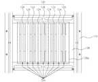
도 1은 본 발명의 일 실시예에 따른 원자층 증착을 위한 가스 공급 모듈에 있어서, 가스 공급 모듈의 상부 단면을 도시한 사시도이다.
도 2는 본 발명의 일 실시예에 따른 원자층 증착을 위한 가스 공급 모듈에 있어서, 가스 공급 모듈의 하부 단면을 도시한 평면도이다.
도 3은 도 1의 가스 공급 모듈의 A-A' 단면을 도시한 평면도이다.
도 4는 본 발명의 일 실시예에 있어서, 가스 공급 모듈의 내부 구조를 도시한 평면도이다.
도 5a 내지 도 5c는 본 발명의 일 실시예에 있어서, 퍼지 가스 공급부와 증착 대상 기판 간의 이격거리에 따른 유체의 흐름에 관한 실험 결과를 나타낸 그래프이다.
도 6은 본 발명의 일 실시예에 있어서, 가스 공급부의 가스 확산영역을 통해 증착 가스가 분사되는 과정을 설명하기 위해 도시한 도면이다.1 is a perspective view of a gas supply module for atomic layer deposition according to an embodiment of the present invention, showing a top cross-section of a gas supply module.
FIG. 2 is a plan view of a gas supply module for atomic layer deposition according to an embodiment of the present invention, showing a lower section of a gas supply module. FIG.
3 is a plan view showing a cross-section AA 'of the gas supply module of FIG.
4 is a plan view showing an internal structure of a gas supply module in an embodiment of the present invention.
FIGS. 5A through 5C are graphs showing experimental results on the flow of a fluid according to a separation distance between a purge gas supply unit and a substrate to be deposited, in an embodiment of the present invention. FIG.
FIG. 6 is a view illustrating a process of spraying a deposition gas through a gas diffusion region of a gas supply unit according to an embodiment of the present invention. Referring to FIG.
본 발명의 이점 및/또는 특징, 그리고 그것들을 달성하는 방법은 첨부되는 도면과 함께 상세하게 후술되어 있는 실시예들을 참조하면 명확해질 것이다. 그러나, 본 발명은 이하에서 개시되는 실시예들에 한정되는 것이 아니라 서로 다른 다양한 형태로 구현될 것이며, 단지 본 실시예들은 본 발명의 개시가 완전하도록 하며, 본 발명이 속하는 기술분야에서 통상의 지식을 가진 자에게 발명의 범주를 완전하게 알려주기 위해 제공되는 것이며, 본 발명은 청구항의 범주에 의해 정의될 뿐이다. 명세서 전체에 걸쳐 동일 참조 부호는 동일 구성요소를 지칭한다.BRIEF DESCRIPTION OF THE DRAWINGS The advantages and / or features of the present invention, and how to accomplish them, will become apparent with reference to the embodiments described in detail below with reference to the accompanying drawings. It should be understood, however, that the invention is not limited to the disclosed embodiments, but is capable of many different forms and should not be construed as limited to the embodiments set forth herein. Rather, these embodiments are provided so that this disclosure will be thorough and complete, To fully disclose the scope of the invention to those skilled in the art, and the invention is only defined by the scope of the claims. Like reference numerals refer to like elements throughout the specification.
이하에서는 첨부된 도면을 참조하여 본 발명의 실시예들을 상세히 설명하기로 한다.Hereinafter, embodiments of the present invention will be described in detail with reference to the accompanying drawings.
본 발명의 일 실시 예에 따른 원자층 증착 장비 가스 모듈은 다양한 박막층을 형성할 수 있다. 예를 들어, 금속 박막층, 산화물 박막층, 질화물 박막층, 탄화물 박막층, 황화물 박막층 중 적어도 하나의 박막층을 형성할 수 있다. 일 실시 예에 따르면, 금속 박막층을 형성하기 위한, 소스 가스는, TMA(TriMethyl Aluminium), TEA(Tri Ethyl Aluminium) 및 DMACl(Di Methyl Aluminum Chloride) 중 하나이고, 반응 가스는, 산소 가스 및 오존 가스 중 하나일 수 있다. 이때 퍼지 가스는, 아르곤(Ar)이나 질소(N2), 헬륨(He) 중 어느 하나의 가스 또는 둘 이상 혼합된 가스가 사용될 수 있다. 다른 실시 예에 따르면, 실리콘 박막층을 형성하기 위한, 소스 가스는, 리콘을 포함하는 실란(Silane, SiH4), 디실란(Disilane, Si2H6) 및 사불화 실리콘(SiF4) 중 하나일 수 있고, 반응 가스는, 산소 가스 및 오존 가스 중 하나일 수 있다. 이 때 퍼지 가스는, 아르곤(Ar)이나 질소(N2), 헬륨(He) 중 어느 하나의 가스 또는 둘 이상 혼합된 가스가 사용될 수 있다. 이 때, 소스 가스, 퍼지 가스, 반응 가스는 이에 한정되는 것은 아니며 당업자의 요구에 따라 변경될 수 있음은 물론이다.The atomic layer deposition equipment gas module according to an embodiment of the present invention can form various thin film layers. For example, at least one thin film layer of a metal thin film layer, an oxide thin film layer, a nitride thin film layer, a carbide thin film layer, and a sulfide thin film layer can be formed. According to one embodiment, the source gas for forming the metal thin film layer is one of TMA (TriMethyl Aluminum), TEA (Tri Ethyl Aluminum) and DMACl (Di Methyl Aluminum Chloride), and the reactive gas is oxygen gas and ozone gas ≪ / RTI > At this time, the purge gas may be any one of argon (Ar), nitrogen (N2), and helium (He) or a mixture of two or more gases. According to another embodiment, the source gas for forming the silicon thin film layer may be one of silane (SiH4), disilane (Si2H6) and silicon tetrafluoride (SiF4) containing ricons, May be one of an oxygen gas and an ozone gas. At this time, the purge gas may be any one of argon (Ar), nitrogen (N2), and helium (He), or a mixture of two or more gases. At this time, the source gas, the purge gas, and the reaction gas are not limited to these, and may be changed according to the needs of those skilled in the art.
본 발명의 일 실시예에 따른 원자층 증착을 위한 가스 공급 모듈은 원자층 박막이 증착되기 위한 증착 대상 기판으로 가스를 분사하기 위한 모듈로서, 케이스 및 케이스의 내부에 구비되는 가스 공급부를 포함하여 구성될 수 있다. 케이스의 상부에는 가스의 석션을 위한 석션 모듈(미도시)이 장착될 수 있는데, 본 실시예에서는 5개의 석션 모듈이 장착될 수 있다. 가스 공급부는 소스 가스, 퍼지 가스 및 반응 가스를 포함하는 원자층 증착 가스를 증착 대상 기판의 다른 영역에 분사한다. 이하에서는, 도 1 내지 도 4를 참조하여, 가스 공급부에 관하여 보다 자세히 설명하고자 한다.A gas supply module for atomic layer deposition according to an embodiment of the present invention is a module for injecting gas into a substrate to be deposited for depositing an atomic layer thin film and includes a case and a gas supply unit provided inside the case, . A suction module (not shown) for suctioning the gas may be mounted on the upper portion of the case. In this embodiment, five suction modules may be mounted. The gas supply unit injects an atomic layer deposition gas containing a source gas, a purge gas, and a reactive gas into another region of the substrate to be deposited. Hereinafter, with reference to Figs. 1 to 4, the gas supply unit will be described in more detail.
도 1은 본 발명의 일 실시예에 따른 원자층 증착을 위한 가스 공급 모듈에 있어서, 가스 공급 모듈의 상부 단면을 도시한 사시도이고, 도 2는 본 발명의 일 실시예에 따른 원자층 증착을 위한 가스 공급 모듈에 있어서, 가스 공급 모듈의 하부 단면을 도시한 평면도이고, 도 3은 도 1의 가스 공급 모듈의 A-A' 단면을 도시한 평면도이고, 도 4는 본 발명의 일 실시예에 있어서, 가스 공급 모듈의 내부 구조를 도시한 평면도이다.FIG. 1 is a perspective view illustrating a gas supply module for atomic layer deposition according to an embodiment of the present invention, and FIG. 2 is a cross- FIG. 3 is a plan view showing a cross-section taken along the line AA 'of the gas supply module of FIG. 1, and FIG. 4 is a cross- Fig. 7 is a plan view showing the internal structure of the supply module.
도 1 및 도 2를 참조하면, 가스 공급 모듈의 가스 공급부(120)는 소스 가스를 분사하는 소스 가스 공급부(122), 퍼지 가스를 공급하는 퍼지 가스 공급부(124) 및 반응 가스를 분사하는 반응 가스 공급부(126)를 포함할 수 있다. 각각의 가스 공급부(120)는 케이스(110) 내에서 서로 일렬로 배치될 수 있다. 즉, 소스 가스 공급부(122), 퍼지 가스 공급부(124) 및 반응 가스 공급부(126)는 케이스(110)의 길이방향을 따라 일정 간격으로 나란히 배치될 수 있다.1 and 2, the
한편, 본 실시예에서는 가스 공급부(120)를 둘러싸도록 가스 공급부(120)의 외곽에 외측 퍼지 가스 공급부(128)가 배치될 수 있다. 외측 퍼지 가스 공급부(128)는 가스 공급부(120)의 둘레방향을 따라 서로 연통되어 형성될 수 있다. 이에 따라, 외측 퍼지 가스 공급부(128)를 통해 분사되는 퍼지 가스가 기체 장벽의 역할을 수행함으로써, 가스가 공급되는 내부 공간 및 공급되지 않는 외부 공간을 분리시킬 수 있다. 즉, 가스가 공급되는 내부 공간을 외부 환경으로부터 고립시켜 고품질의 원자층 증착이 이루어지는 환경을 마련할 수 있다. 뿐만 아니라, 진공의 환경이 아닌 상압에서도 원자층 증착이 이루어질 수 있으며 roll to roll 공법의 적용이 가능하다.Meanwhile, in the present embodiment, the outer purge
참고로, 외측 퍼지 가스 공급부(128)는 도 4에 도시된 바와 같이 타측에 구비된 분사홀(128a)을 통해 증착 대상 기판(W)을 향하여 퍼지 가스를 분사할 수 있다.For reference, the outer purge
도 3을 참조하면, 가스 공급부(120)는 일측 예를 들어, 상측에 가스를 제공하는 가스 공급원이 장착될 수 있고, 타측 예를 들어, 하측에 증착 대상 기판(W)이 소정 간격 이격되어 배치될 수 있다.Referring to FIG. 3, the
증착 대상 기판(W)의 하측에는 기판이 안착되는 안착부(미도시)를 포함하는 스테이지(130)가 마련될 수 있다. 스테이지(130)는 안착된 증착 대상 기판(W)을 회전시킬 수 있다. 이에 따라, 스테이지(130)의 회전에 의하여 증착 대상 기판(W)이 가스 공급부(120)의 아래를 통과하므로, 원자층 증착 가스를 공급받아 증착 대상 기판(W)에는 원자층 박막이 증착될 수 있다. 참고로, 증착 대상 기판(W)은 웨이퍼와 같은 원형뿐만 아니라 다양한 형상을 가질 수 있음은 물론이다.A
가스 공급부(120)는 제1 및 제2 소스 가스 공급부(122a, 122b)와 제1 내지 제4 퍼지 가스 공급부(124a, 124b, 124c, 124d)와 제1 내지 제3 반응 가스 공급부(126a, 126b, 126c)를 포함할 수 있다. 이때, 제1 및 제2 소스 가스 공급부(122a, 122b)와 제1 내지 제4 퍼지 가스 공급부(124a, 124b, 124c, 124d)와 제1 내지 제3 반응 가스 공급부(126a, 126b, 126c)는 증착 대상 기판(W)의 회전 방향을 따라 배치될 수 있다. 구체적으로, 제1 반응 가스 공급부(126a), 제1 퍼지 가스 공급부(124a), 제1 소스 가스 공급부(122a), 제2 퍼지 가스 공급부(124b), 제2 반응 가스 공급부(126b), 제3 퍼지 가스 공급부(124c), 제2 소스 가스 공급부(122b), 제4 퍼지 가스 공급부(124d), 제3 반응 가스 공급부(126c) 순서로 배치될 수 있다. 참고로, 상기 배치 순서의 처음과 끝에 외측 퍼지 가스 공급부(128)가 배치될 수 있다. 즉, 외측 퍼지 가스 공급부(128), 제1 반응 가스 공급부(126a), 제1 퍼지 가스 공급부(124a), 제1 소스 가스 공급부(122a), 제2 퍼지 가스 공급부(124b), 제2 반응 가스 공급부(126b), 제3 퍼지 가스 공급부(124c), 제2 소스 가스 공급부(122b), 제4 퍼지 가스 공급부(124d), 제3 반응 가스 공급부(126c), 외측 퍼지 가스 공급부(128) 순서로 배치될 수 있다.The
제1 및 제2 소스 가스 공급부(122a, 122b)는 소스 가스 공급원(미도시)로부터 소스 가스를 제공받고, 제공받은 소스 가스를 증착 대상 기판(W)을 향하여 분사할 수 있다. 제1 내지 제4 퍼지 가스 공급부(124a, 124b, 124c, 124d)는 퍼지 가스 공급원(미도시)로부터 퍼지 가스를 제공받고, 제공받은 퍼지 가스를 증착 대상 기판(W)을 향하여 분사할 수 있다. 또한, 제1 내지 제3 반응 가스 공급부(126a, 126b, 126c)는 반응 가스 공급원(미도시)로부터 반응 가스를 제공받고, 제공받은 반응 가스를 증착 대상 기판(W)을 향하여 분사할 수 있다.The first and second source
본 실시예에 따르면, 각 가스 공급부(120)는 스테이지(130)의 중심부보다 주변부에서 더 많은 증착 가스를 분사하도록 구성될 수 있다. 예를 들어, 각 가스 공급부의(120) 분사구는 스테이지(130)의 중심부보다 주변부에서 더 클 수 있다. 이는, 스테이지(130)의 각 속도가 동일한 경우, 스테이지(130)의 중심부보다 반경 방향으로 외측에 위치한 주변부의 선 속도가 더 크다는 점을 고려한 것이다. 이로써, 스테이지(130)의 중심부에 위치한 증착 대상 기판(W)의 영역이나 스테이지(130)의 주변부에 위치한 증착 대상 기판(W)의 영역에 일정한 원자층 박막이 증착될 수 있다.According to the present embodiment, each
제1 소스 가스 공급부(122a)의 양측에는 제1 소스 가스 공급부(122a)에서 분사된 소스 가스를 배기하는 배기구(122c)가 인접하여 배치될 수 있고, 제2 소스 가스 공급부(122b)의 양측에는 제2 소스 가스 공급부(122b)에서 분사된 소스 가스를 배기하는 배기구(122c)가 인접하여 배치될 수 있다. 각 배기구(122c)는 분사된 소스 가스를 분사 방향과 역 방향으로 회수함으로써, 소스 가스가 선택된 분사 영역 외의 타 영역으로 진입하는 것을 방지할 수 있다. 제1 반응 가스 공급부(126a)의 양측에는 제1 반응 가스 공급부(126a)에서 분사된 반응 가스를 배기하는 배기구(126d)가 인접하여 배치될 수 있고, 제2 반응 가스 공급부(126b)의 양측에는 제2 반응 가스 공급부(126a)에서 분사된 반응 가스를 배기하는 배기구(126d)가 인접하여 배치될 수 있고, 제3 반응 가스 공급부(126c)의 양측에는 제3 반응 가스 공급부(126c)에서 분사된 반응 가스를 배기하는 배기구(126d)가 인접하여 배치될 수 있다. 각 배기구(126d)는 분사된 반응 가스를 분사 방향과 역 방향으로 회수함으로써, 반응 가스가 선택된 분사 영역 외의 타 영역으로 진입하는 것을 방지할 수 있다.An exhaust port 122c for exhausting the source gas injected from the first source
배기구(122c, 126d)는 바 드라이 펌프(bar dry pump, 미도시)와 연통할 수 있다. 바 드라이 펌프의 구동에 의하여, 탑 펌핑(top pumping) 방식으로 분사된 소스 가스 및/또는 반응 가스 중 기판의 해당 영역을 벗어나는 소스 가스 및/또는 반응 가스는 배기될 수 있다.The exhaust ports 122c and 126d can communicate with a bar dry pump (not shown). By the driving of the bar dry pump, the source gas and / or the reactive gas out of the corresponding region of the substrate among the source gas and / or reactive gas injected in the top pumping manner can be exhausted.
도 4를 참조하면, 가스 공급부(120)는 케이스(110)의 높이방향을 기준으로 각각 상이한 높이를 가질 수 있다. 구체적으로, 퍼지 가스 공급부(124)의 높이는 소스 가스 공급부(122)의 높이 및 반응 가스 공급부(126)의 높이 보다 높을 수 있다. 다시 말해, 퍼지 가스 공급부(124)와 증착 대상 기판(W) 간의 이격거리(h2)는 반응 가스 공급부(126)와 증착 대상 기판(W) 간의 이격거리(h1) 및 소스 가스 공급부(122)와 증착 대상 기판(W) 간의 이격거리(h2) 보다 작을 수 있다. 즉, 퍼지 가스 공급부(124)와 소스 가스 공급부(122) 및 반응 가스 공급부(126)의 높이 차이에 따른 갭(gap)으로 인해 물리적 장벽이 형성될 수 있다. 이에 따라, 퍼지 가스 공급부(124)로부터 분사되는 퍼지 가스가 에어 커튼의 역할을 수행함으로써 소스 가스 및 반응 가스의 혼입을 방지할 수 있다.Referring to FIG. 4, the
이와 관련하여, 본 실시예에서는 퍼지 가스 공급부(124)와 증착 대상 기판(W) 간의 이격거리(h2)에 따른 유체의 흐름을 알아보기 위한 실험을 진행하였다. 도 5a 내지 도 5c를 참조하면, 퍼지 가스 공급부(124)와 증착 대상 기판(W) 간의 이격거리(h2)를 각각 다르게 구현하여 실험하였는데 구체적으로, 도 5a에서와 같이 이격거리(h2)가 큰 경우, 도 5b에서와 같이 이격거리(h2)가 보통인 경우 및 도 5c에서와 같이 이격거리(h2)가 작은 경우로 나누어 실험하였다. 실험한 결과, 퍼지 가스 공급부(124)와 증착 대상 기판(W) 간의 이격거리(h2)를 보통으로 설정한 경우에 유체의 흐름이 활발해지는 것을 확인하였다. 이를 통해, 퍼지 가스 공급부(124)와 증착 대상 기판(W) 간의 이격거리(h2)를 소스 가스 공급부(122)와 증착 대상 기판(W) 간의 이격거리(h1) 및 반응 가스 공급부(126)와 증착 대상 기판(W) 간의 이격거리(h1)와의 차이보다 너무 크지도 작지도 않은 적당하게 설정함으로써, 증착이 효율적으로 이루어질 수 있다. 참고로, 도 5a 내지 도 5c는 본 발명의 일 실시예에 있어서, 퍼지 가스 공급부(124)와 증착 대상 기판(W) 간의 이격거리(h2)에 따른 유체의 흐름에 관한 실험 결과를 나타낸 그래프이다.In this regard, in the present embodiment, an experiment was conducted to determine the flow of the fluid according to the separation distance h2 between the purge
가스 공급부(120)는 케이스(110)의 높이방향을 기준으로 다단의 형태를 가지며 형성될 수 있다. 즉, 가스 공급부(120)는 케이스(110)의 내부에서 케이스(110)의 일측 예를 들어, 상측과 케이스(110)의 타측 예를 들어, 하측의 사이에서 증착 가스가 공급되는 경로인 특정 공간을 포함하여 구성될 수 있다. 구체적으로, 가스 공급부(120)는 제1 내지 제3 가스 확산영역(10, 20, 30)을 포함하여 구성될 수 있다.The
제1 가스 확산영역(10)은 가스 공급부(120)의 상부에 형성되는 공간일 수 있고, 제2 가스 확산영역(20)은 소스 가스 공급부(122) 및 반응 가스 공급부(126)의 내부에 형성되며, 제1 가스 확산영역(10)과 연결되는 공간일 수 있고, 제3 가스 확산영역(30)은 소스 가스 공급부(122) 및 반응 가스 공급부(126)의 내부에 형성되며, 제2 가스 확산영역(20)과 연결되는 공간일 수 있다. 이때, 증착 가스는 제1 가스 확산영역(10), 제2 가스 확산영역(20) 및 제3 가스 확산영역(30)을 차례로 통과하여 증착 대상 기판(W)을 향하여 분사될 수 있다.The first
제1 내지 제3 가스 확산영역(10, 20, 30)은 각 영역 사이에 구비되는 격벽을 포함할 수 있다. 구체적으로, 도 6에 도시된 바와 같이, 제1 가스 확산영역(10) 및 제2 가스 확산영역(20)의 사이에는 제1 격벽(12)이 구비될 수 있고, 제2 가스 확산영역(20) 및 제3 가스 확산영역(30)의 사이에는 제2 격벽(22)이 구비될 수 있고, 제3 가스 확산영역(30)의 하부에는 제3 격벽(32)이 구비될 수 있다. 참고로, 도 6은 본 발명의 일 실시예에 있어서, 가스 공급부(120)의 가스 확산영역을 통해 증착 가스가 분사되는 과정을 설명하기 위해 도시한 도면이다.The first to third
제1 내지 제3 격벽(12, 22, 32)은 각각 소정 크기의 확산홀(12a, 22a, 32a)을 구비할 수 있다. 본 실시예에서는, 확산홀(12a, 22a, 32a)을 통해 가스 공급부(120)의 일측 예를 들어, 상측에서 타측 예를 들어, 하측으로 증착 가스를 확산시킬 수 있다. 구체적으로, 증착 가스는 제1 가스 확산영역(10)으로부터 제1 격벽(12)에 구비된 확산홀(12a)을 통해 제2 가스 확산영역(20)으로 확산될 수 있고, 제2 가스 확산영역(20)으로부터 제2 격벽(22)에 구비된 확산홀(22a)을 통해 제3 가스 확산영역(30)으로 확산될 수 있고, 제3 가스 확산영역(30)으로부터 제3 격벽(32)에 구비된 확산홀(32a)을 통해 증착 대상 기판(W)을 향하여 확산되어 분사될 수 있다. 이를 통해, 가스 공급부(120)로 공급되는 증착 가스의 압력을 복수의 확산홀(12a, 22a, 32a)에 고르게 분배시켜 증착 균일도를 향상시킬 수 있다. 뿐만 아니라, 확산홀(12a, 22a, 32a)에 의해 증착 가스가 고르게 분사됨으로써 증착 대상 기판(W)의 두께 또한 균일하게 가공할 수 있다.The first to
확산홀(12a, 22a, 32a)은 제1 내지 제3 격벽(12, 22, 32)의 상하면에 복수로 구비되되, 제1 내지 제3 격벽(12, 22, 32)의 각 길이방향을 따라 일정 간격으로 형성될 수 있다.A plurality of
확산홀(12a, 22a, 32a)은 각 격벽의 일측면 및 타측면의 대응되는 위치에서 서로 마주보도록 형성될 수 있다. 구체적으로, 제1 격벽(12)의 타측면에 형성된 확산홀(12a)은 제2 격벽(22)의 상측면에 형성된 확산홀(22a)과 서로 마주보되 동일한 개수로 형성될 수 있고, 제2 격벽(22)의 하측면에 형성된 확산홀(22a)은 제3 격벽(32)의 상측면에 형성된 확산홀(32a)과 서로 마주보되 동일한 개수로 형성될 수 있다.The diffusion holes 12a, 22a, and 32a may be formed to face each other at a corresponding position on one side surface and the other side surface of each partition wall. Specifically, the
확산홀(12a, 22a, 32a)의 개수는 각 격벽마다 상이하며, 하기 수식을 만족할 수 있다.The number of the
[수식][Equation]
제1 격벽(12)에 형성된 확산홀(12a)의 개수 < 제2 격벽(22)에 형성된 확산홀(22a)의 개수 < 제3 격벽(32)에 형성된 확산홀(32a)의 개수.The number of
구체적으로, 제2 격벽(22)의 하측면에 형성된 확산홀(22a)의 개수는 제1 격벽(12)의 상측면 및 하측면에 형성된 확산홀(12a)의 개수보다 많을 수 있고, 제3 격벽(32)의 하측면에 형성된 확산홀(32a)의 개수는 제2 격벽(22)의 상측면 및 하측면에 형성된 확산홀(22a)의 개수보다 많을 수 있다. 예를 들어, 제1 격벽(12)의 상측면 및 하측면에 형성된 확산홀(12a)의 개수는 3~5개이고, 제2 격벽(22)의 하측면에 형성된 확산홀(22a)의 개수는 8~12개이고, 제3 격벽(32)의 하측면에 형성된 확산홀(32a)의 개수는 240~260개일 수 있다. 바람직하게는, 제1 격벽(12)의 상측면 및 하측면에 형성된 확산홀(12a)의 개수는 4개이고, 제2 격벽(22)의 하측면에 형성된 확산홀(22a)의 개수는 10개이고, 제3 격벽(32)의 하측면에 형성된 확산홀(32a)의 개수는 250개일 수 있다. 이로써, 본 실시예에서는, 각 격벽에 구비된 복수의 확산홀(12a, 22a, 32a)을 통해 증착 대상 기판(W)을 향하여 증착 가스를 균일하게 분사할 수 있다.More specifically, the number of the diffusion holes 22a formed on the lower side of the
지금까지 본 발명에 따른 구체적인 실시예에 관하여 설명하였으나, 본 발명의 범위에서 벗어나지 않는 한도 내에서는 여러 가지 변형이 가능함은 물론이다. 그러므로, 본 발명의 범위는 설명된 실시예에 국한되어 정해져서는 안 되며, 후술하는 특허 청구의 범위뿐 아니라 이 특허 청구의 범위와 균등한 것들에 의해 정해져야 한다.While the present invention has been described in connection with what is presently considered to be practical exemplary embodiments, it is to be understood that the invention is not limited to the disclosed embodiments. Therefore, the scope of the present invention should not be limited to the described embodiments, but should be determined by the scope of the appended claims and equivalents thereof.
이상과 같이 본 발명은 비록 한정된 실시예와 도면에 의해 설명되었으나, 본 발명은 상기의 실시예에 한정되는 것은 아니며, 이는 본 발명이 속하는 분야에서 통상의 지식을 가진 자라면 이러한 기재로부터 다양한 수정 및 변형이 가능하다. 따라서, 본 발명 사상은 아래에 기재된 특허청구범위에 의해서만 파악되어야 하고, 이의 균등 또는 등가적 변형 모두는 본 발명 사상의 범주에 속한다고 할 것이다.While the present invention has been particularly shown and described with reference to exemplary embodiments thereof, it is to be understood that the invention is not limited to the disclosed exemplary embodiments, but, on the contrary, Modification is possible. Accordingly, the spirit of the present invention should be understood only in accordance with the following claims, and all equivalents or equivalent variations thereof are included in the scope of the present invention.
10 : 제1 가스 확산영역
12 : 제1 격벽
20 : 제2 가스 확산영역
22 : 제2 격벽
30 : 제1 가스 확산영역
32 : 제1 격벽
110 : 케이스
120 : 가스 공급부
122 : 소스 가스 공급부
122a : 제1 소스 가스 공급부
122b : 제2 소스 가스 공급부
124 : 퍼지 가스 공급부
124a : 제1 퍼지 가스 공급부
124b : 제2 퍼지 가스 공급부
124c : 제3 퍼지 가스 공급부
124d : 제4 퍼지 가스 공급부
126 : 반응 가스 공급부
126a : 제1 반응 가스 공급부
126b : 제2 반응 가스 공급부
126c : 제3 반응 가스 공급부
122c, 126d : 배기구
128 : 외측 퍼지 가스 공급부
12a, 22a, 32a : 확산홀
130 : 스테이지10: first gas diffusion region
12: first partition
20: second gas diffusion region
22: second partition
30: first gas diffusion region
32: first partition
110: Case
120: gas supply unit
122: source gas supply unit
122a: a first source gas supply part
122b: the second source gas supply part
124: purge gas supply unit
124a: first purge gas supply part
124b: the second purge gas supply part
124c: third purge gas supply part
124d: fourth purge gas supply section
126: Reaction gas supply unit
126a: the first reaction gas supply part
126b: the second reaction gas supply part
126c: the third reaction gas supply part
122c, 126d:
128: outer purge gas supply part
12a, 22a, 32a: diffusion holes
130: stage
Claims (10)
Translated fromKorean상기 케이스의 내부에 구비되며, 소스 가스, 퍼지 가스 및 반응 가스를 포함하는 원자층 증착 가스를 동시에 증착 대상 기판의 다른 영역에 분사하는 가스 공급부를 포함하고,
상기 가스 공급부는
상기 케이스의 높이방향을 기준으로 다단의 형태를 가지며 형성되되, 각 단 별로 구비된 확산홀을 통해 상기 원자층 증착 가스를 일측에서 타측으로 확산시키고,
상기 가스 공급부는
상기 소스 가스를 분사하는 소스 가스 공급부, 상기 퍼지 가스를 공급하는 퍼지 가스 공급부 및 상기 반응 가스를 분사하는 반응 가스 공급부를 포함하고,
상기 소스 가스 공급부, 상기 퍼지 가스 공급부 및 상기 반응 가스 공급부는 상기 케이스의 길이방향을 따라 일정 간격으로 서로 나란히 배치되고,
가스가 공급되는 내부 공간 및 가스가 공급되지 않는 외부 공간을 분리시키기 위해, 상기 가스 공급부의 둘레방향을 따라 외곽에 배치되되 서로 연통되어 형성되는 외측 퍼지 가스 공급부를 더 포함하고,
상기 가스 공급부는
상기 가스 공급부의 상부에 형성되는 공간인 제1 가스 확산영역;
상기 소스 가스 공급부 및 상기 반응 가스 공급부의 내부에 형성되며, 상기 제1 가스 확산영역과 연결되는 공간인 제2 가스 확산영역; 및
상기 소스 가스 공급부 및 상기 반응 가스 공급부의 내부에 형성되며, 상기 제2 가스 확산영역과 연결되는 공간인 제3 가스 확산영역을 포함하고,
상기 제1 내지 제3 가스 확산영역은
상기 제1 가스 확산영역 및 상기 제2 가스 확산영역의 사이에 구비되는 제1 격벽;
상기 제2 가스 확산영역 및 상기 제3 가스 확산영역의 사이에 구비되는 제2 격벽; 및
상기 제3 가스 확산영역의 하부에 구비되는 제3 격벽을 포함하고,
상기 확산홀은 상기 제1 내지 제3 격벽의 상하면에 복수로 구비되되 상기 제1 내지 제3 격벽의 길이방향을 따라 일정 간격으로 형성되며 각 격벽의 일측면 및 타측면의 대응되는 위치에서 서로 마주보도록 형성되고,
상기 확산홀의 개수는 하기 수식을 만족하는 것을 특징으로 하는 원자층 증착을 위한 가스 공급 모듈.
[수식]
상기 제1 격벽에 형성된 확산홀의 개수 < 상기 제2 격벽에 형성된 확산홀의 개수 < 상기 제3 격벽에 형성된 확산홀의 개수.
case; And
And a gas supply unit provided in the case and injecting an atomic layer deposition gas containing a source gas, a purge gas, and a reactive gas into another region of the substrate to be vaporized at the same time,
The gas supply part
The atomic layer deposition gas is diffused from one side to the other side through diffusion holes provided for each stage,
The gas supply part
A purge gas supply unit for supplying the purge gas and a reaction gas supply unit for spraying the reaction gas,
Wherein the source gas supply unit, the purge gas supply unit, and the reaction gas supply unit are arranged side by side at regular intervals along the longitudinal direction of the case,
Further comprising an outer purge gas supply unit disposed at an outer periphery along the circumferential direction of the gas supply unit and communicating with each other for separating an inner space to which gas is supplied and an outer space to which no gas is supplied,
The gas supply part
A first gas diffusion region that is a space formed in an upper portion of the gas supply unit;
A second gas diffusion region formed in the source gas supply unit and the reaction gas supply unit, the second gas diffusion region being a space connected to the first gas diffusion region; And
And a third gas diffusion region formed in the source gas supply unit and the reaction gas supply unit, the third gas diffusion region being a space connected to the second gas diffusion region,
The first to third gas diffusion regions
A first gas barrier provided between the first gas diffusion region and the second gas diffusion region;
A second gas barrier provided between the second gas diffusion region and the third gas diffusion region; And
And a third partition disposed below the third gas diffusion region,
The diffusion holes are formed at a plurality of positions on the upper and lower surfaces of the first to third barrier ribs. The diffusion holes are formed at regular intervals along the longitudinal direction of the first to third barrier ribs, Lt; / RTI >
Characterized in that the number of diffusion holes satisfies the following equation.
[Equation]
The number of diffusion holes formed in the first bank, the number of diffusion holes formed in the second bank, and the number of diffusion holes formed in the third bank.
상기 제1 격벽에 형성된 확산홀의 개수는 3~5개이고, 상기 제2 격벽에 형성된 확산홀의 개수는 8~12개이고, 상기 제3 격벽에 형성된 확산홀의 개수는 240~260개인 것을 특징으로 하는 원자층 증착을 위한 가스 공급 모듈.
The method according to claim 1,
Wherein the number of diffusion holes formed in the first barrier rib is 3 to 5, the number of diffusion holes formed in the second barrier rib is 8 to 12, and the number of diffusion holes formed in the third barrier rib is 240 to 260. Gas supply module for deposition.
상기 가스 공급부의 타측에는 상기 증착 대상 기판이 마련되고,
상기 퍼지 가스 공급부와 상기 증착 대상 기판 간의 이격거리는
상기 반응 가스 공급부와 상기 증착 대상 기판 간의 이격거리 및 상기 소스 가스 공급부와 상기 증착 대상 기판 간의 이격거리 보다 작은 것을 특징으로 하는 원자층 증착을 위한 가스 공급 모듈.The method according to claim 1,
The substrate to be vapor-deposited is provided on the other side of the gas supply unit,
The separation distance between the purge gas supply unit and the deposition target substrate
Wherein the distance between the reaction gas supply unit and the deposition target substrate is smaller than the distance between the source gas supply unit and the deposition target substrate.
Priority Applications (2)
| Application Number | Priority Date | Filing Date | Title |
|---|---|---|---|
| KR1020170048384AKR101972389B1 (en) | 2017-04-14 | 2017-04-14 | Gas supply module for atomic layer deposition |
| PCT/KR2018/004393WO2018190696A1 (en) | 2017-04-14 | 2018-04-16 | Gas supply module for atomic layer deposition |
Applications Claiming Priority (1)
| Application Number | Priority Date | Filing Date | Title |
|---|---|---|---|
| KR1020170048384AKR101972389B1 (en) | 2017-04-14 | 2017-04-14 | Gas supply module for atomic layer deposition |
Publications (2)
| Publication Number | Publication Date |
|---|---|
| KR20180115912A KR20180115912A (en) | 2018-10-24 |
| KR101972389B1true KR101972389B1 (en) | 2019-04-25 |
Family
ID=63792737
Family Applications (1)
| Application Number | Title | Priority Date | Filing Date |
|---|---|---|---|
| KR1020170048384AActiveKR101972389B1 (en) | 2017-04-14 | 2017-04-14 | Gas supply module for atomic layer deposition |
Country Status (2)
| Country | Link |
|---|---|
| KR (1) | KR101972389B1 (en) |
| WO (1) | WO2018190696A1 (en) |
Families Citing this family (4)
| Publication number | Priority date | Publication date | Assignee | Title |
|---|---|---|---|---|
| KR102746990B1 (en)* | 2021-02-08 | 2024-12-27 | 주식회사 넥서스비 | Roll-to-roll atomic layer depositing apparatus |
| WO2022169065A1 (en)* | 2021-02-08 | 2022-08-11 | 주식회사 넥서스비 | Roll-to-roll atomic layer deposition apparatus |
| KR102761054B1 (en) | 2021-12-29 | 2025-02-04 | 주식회사 넥서스비 | Atmoic layer depositing apparatus and atmoic layer depositing method using the same |
| CN115821229A (en)* | 2022-11-25 | 2023-03-21 | 江苏微导纳米科技股份有限公司 | A method and apparatus for depositing thin films and thin films |
Family Cites Families (8)
| Publication number | Priority date | Publication date | Assignee | Title |
|---|---|---|---|---|
| KR20090097401A (en)* | 2008-03-11 | 2009-09-16 | (주)퓨전에이드 | Deposition apparatus and deposition method using the same |
| EP2159304A1 (en)* | 2008-08-27 | 2010-03-03 | Nederlandse Organisatie voor toegepast- natuurwetenschappelijk onderzoek TNO | Apparatus and method for atomic layer deposition |
| KR20110076386A (en) | 2009-12-29 | 2011-07-06 | 세메스 주식회사 | Atomic Layer Deposition Equipment Used in Semiconductor Manufacturing |
| KR102070400B1 (en)* | 2012-06-29 | 2020-01-28 | 주성엔지니어링(주) | Apparatus and method for processing substrate |
| KR101526861B1 (en)* | 2013-08-16 | 2015-06-09 | 주식회사 테스 | Gas supply unit and thin film deposition apparatus having the same |
| KR102150361B1 (en)* | 2014-02-19 | 2020-09-01 | 주식회사 케이씨텍 | Atomic layer deposition apparatus |
| KR20160053493A (en)* | 2014-11-05 | 2016-05-13 | 주식회사 케이씨텍 | Gas supplying device and atomic layer deposition apparatus having the same |
| KR20160134908A (en)* | 2015-05-13 | 2016-11-24 | 참엔지니어링(주) | Substrate processing apparatus |
- 2017
- 2017-04-14KRKR1020170048384Apatent/KR101972389B1/enactiveActive
- 2018
- 2018-04-16WOPCT/KR2018/004393patent/WO2018190696A1/ennot_activeCeased
Also Published As
| Publication number | Publication date |
|---|---|
| WO2018190696A1 (en) | 2018-10-18 |
| KR20180115912A (en) | 2018-10-24 |
Similar Documents
| Publication | Publication Date | Title |
|---|---|---|
| KR101021372B1 (en) | Atomic layer deposition apparatus | |
| KR101972389B1 (en) | Gas supply module for atomic layer deposition | |
| US20100319853A1 (en) | Gas supply device and apparatus for processing a substrate | |
| CN101994101A (en) | Film deposition apparatus and film deposition method | |
| CN101736318A (en) | Film deposition apparatus | |
| TW201324663A (en) | Precursor distribution features for improved deposition uniformity | |
| TWI586827B (en) | Manufacturing method for film and atomic layer deposition apparatus | |
| KR20010081936A (en) | Method for manufacturing a semiconductor device and apparatus for manufacturing a semiconductor | |
| KR100946159B1 (en) | Thin film deposition equipment | |
| KR100920324B1 (en) | Thin film deposition equipment | |
| KR100949913B1 (en) | Atomic layer deposition apparatus | |
| KR101485580B1 (en) | Atomic layer deposition apparatus | |
| CN105453224A (en) | Substrate processing equipment | |
| KR100908987B1 (en) | Substrate Support of Thin Film Deposition Equipment | |
| KR100982842B1 (en) | Atomic layer deposition apparatus | |
| KR101028407B1 (en) | Atomic layer deposition apparatus | |
| KR101265905B1 (en) | Exhaust gas separating exhausted atomic layer deposition apparatus | |
| US7883746B2 (en) | Insulating film formation method which exhibits improved thickness uniformity and improved composition uniformity | |
| KR100901118B1 (en) | Injection unit of thin film deposition apparatus | |
| KR101493250B1 (en) | Atomic layer deposition apparatus | |
| KR20100077695A (en) | Atomic layer deposition apparatus | |
| KR101885525B1 (en) | Atomic Layer Deposition Apparatus and Deposition Method Using the Same | |
| KR101493254B1 (en) | Atomic layer deposition apparatus | |
| KR20110042588A (en) | Process Module for Atomic Layer Deposition Equipment | |
| KR20180054448A (en) | Film forming apparatus |
Legal Events
| Date | Code | Title | Description |
|---|---|---|---|
| A201 | Request for examination | ||
| PA0109 | Patent application | Patent event code:PA01091R01D Comment text:Patent Application Patent event date:20170414 | |
| PA0201 | Request for examination | ||
| E902 | Notification of reason for refusal | ||
| PE0902 | Notice of grounds for rejection | Comment text:Notification of reason for refusal Patent event date:20180808 Patent event code:PE09021S01D | |
| AMND | Amendment | ||
| PG1501 | Laying open of application | ||
| E601 | Decision to refuse application | ||
| PE0601 | Decision on rejection of patent | Patent event date:20190207 Comment text:Decision to Refuse Application Patent event code:PE06012S01D Patent event date:20180808 Comment text:Notification of reason for refusal Patent event code:PE06011S01I | |
| AMND | Amendment | ||
| PX0901 | Re-examination | Patent event code:PX09011S01I Patent event date:20190207 Comment text:Decision to Refuse Application Patent event code:PX09012R01I Patent event date:20181008 Comment text:Amendment to Specification, etc. | |
| PX0701 | Decision of registration after re-examination | Patent event date:20190409 Comment text:Decision to Grant Registration Patent event code:PX07013S01D Patent event date:20190311 Comment text:Amendment to Specification, etc. Patent event code:PX07012R01I Patent event date:20190207 Comment text:Decision to Refuse Application Patent event code:PX07011S01I Patent event date:20181008 Comment text:Amendment to Specification, etc. Patent event code:PX07012R01I | |
| X701 | Decision to grant (after re-examination) | ||
| PR0701 | Registration of establishment | Comment text:Registration of Establishment Patent event date:20190419 Patent event code:PR07011E01D | |
| PR1002 | Payment of registration fee | Payment date:20190422 End annual number:3 Start annual number:1 | |
| PG1601 | Publication of registration | ||
| PR1001 | Payment of annual fee | Payment date:20220801 Start annual number:4 End annual number:4 | |
| PR1001 | Payment of annual fee | Payment date:20230621 Start annual number:5 End annual number:5 | |
| PR1001 | Payment of annual fee | Payment date:20240219 Start annual number:6 End annual number:6 |