KR101971863B1 - Semiconductor device - Google Patents
Semiconductor deviceDownload PDFInfo
- Publication number
- KR101971863B1 KR101971863B1KR1020180071175AKR20180071175AKR101971863B1KR 101971863 B1KR101971863 B1KR 101971863B1KR 1020180071175 AKR1020180071175 AKR 1020180071175AKR 20180071175 AKR20180071175 AKR 20180071175AKR 101971863 B1KR101971863 B1KR 101971863B1
- Authority
- KR
- South Korea
- Prior art keywords
- transistor
- insulating layer
- electrode
- layer
- region
- Prior art date
- Legal status (The legal status is an assumption and is not a legal conclusion. Google has not performed a legal analysis and makes no representation as to the accuracy of the status listed.)
- Expired - Fee Related
Links
Images


Classifications
- H—ELECTRICITY
- H10—SEMICONDUCTOR DEVICES; ELECTRIC SOLID-STATE DEVICES NOT OTHERWISE PROVIDED FOR
- H10B—ELECTRONIC MEMORY DEVICES
- H10B41/00—Electrically erasable-and-programmable ROM [EEPROM] devices comprising floating gates
- H10B41/30—Electrically erasable-and-programmable ROM [EEPROM] devices comprising floating gates characterised by the memory core region
- H—ELECTRICITY
- H10—SEMICONDUCTOR DEVICES; ELECTRIC SOLID-STATE DEVICES NOT OTHERWISE PROVIDED FOR
- H10B—ELECTRONIC MEMORY DEVICES
- H10B10/00—Static random access memory [SRAM] devices
- H10B10/12—Static random access memory [SRAM] devices comprising a MOSFET load element
- H10B10/125—Static random access memory [SRAM] devices comprising a MOSFET load element the MOSFET being a thin film transistor [TFT]
- H01L27/11521—
- G—PHYSICS
- G11—INFORMATION STORAGE
- G11C—STATIC STORES
- G11C16/00—Erasable programmable read-only memories
- G11C16/02—Erasable programmable read-only memories electrically programmable
- G11C16/04—Erasable programmable read-only memories electrically programmable using variable threshold transistors, e.g. FAMOS
- G11C16/0408—Erasable programmable read-only memories electrically programmable using variable threshold transistors, e.g. FAMOS comprising cells containing floating gate transistors
- H—ELECTRICITY
- H01—ELECTRIC ELEMENTS
- H01L—SEMICONDUCTOR DEVICES NOT COVERED BY CLASS H10
- H01L21/00—Processes or apparatus adapted for the manufacture or treatment of semiconductor or solid state devices or of parts thereof
- H01L21/02—Manufacture or treatment of semiconductor devices or of parts thereof
- H01L21/04—Manufacture or treatment of semiconductor devices or of parts thereof the devices having potential barriers, e.g. a PN junction, depletion layer or carrier concentration layer
- H01L21/18—Manufacture or treatment of semiconductor devices or of parts thereof the devices having potential barriers, e.g. a PN junction, depletion layer or carrier concentration layer the devices having semiconductor bodies comprising elements of Group IV of the Periodic Table or AIIIBV compounds with or without impurities, e.g. doping materials
- H01L21/30—Treatment of semiconductor bodies using processes or apparatus not provided for in groups H01L21/20 - H01L21/26
- H01L21/31—Treatment of semiconductor bodies using processes or apparatus not provided for in groups H01L21/20 - H01L21/26 to form insulating layers thereon, e.g. for masking or by using photolithographic techniques; After treatment of these layers; Selection of materials for these layers
- H01L21/3105—After-treatment
- H01L21/31051—Planarisation of the insulating layers
- H01L27/0688—
- H01L27/11551—
- H01L27/1156—
- H01L27/1225—
- H01L28/60—
- H—ELECTRICITY
- H10—SEMICONDUCTOR DEVICES; ELECTRIC SOLID-STATE DEVICES NOT OTHERWISE PROVIDED FOR
- H10B—ELECTRONIC MEMORY DEVICES
- H10B41/00—Electrically erasable-and-programmable ROM [EEPROM] devices comprising floating gates
- H10B41/20—Electrically erasable-and-programmable ROM [EEPROM] devices comprising floating gates characterised by three-dimensional arrangements, e.g. with cells on different height levels
- H—ELECTRICITY
- H10—SEMICONDUCTOR DEVICES; ELECTRIC SOLID-STATE DEVICES NOT OTHERWISE PROVIDED FOR
- H10B—ELECTRONIC MEMORY DEVICES
- H10B41/00—Electrically erasable-and-programmable ROM [EEPROM] devices comprising floating gates
- H10B41/70—Electrically erasable-and-programmable ROM [EEPROM] devices comprising floating gates the floating gate being an electrode shared by two or more components
- H—ELECTRICITY
- H10—SEMICONDUCTOR DEVICES; ELECTRIC SOLID-STATE DEVICES NOT OTHERWISE PROVIDED FOR
- H10D—INORGANIC ELECTRIC SEMICONDUCTOR DEVICES
- H10D1/00—Resistors, capacitors or inductors
- H10D1/60—Capacitors
- H10D1/68—Capacitors having no potential barriers
- H10D1/692—Electrodes
- H—ELECTRICITY
- H10—SEMICONDUCTOR DEVICES; ELECTRIC SOLID-STATE DEVICES NOT OTHERWISE PROVIDED FOR
- H10D—INORGANIC ELECTRIC SEMICONDUCTOR DEVICES
- H10D86/00—Integrated devices formed in or on insulating or conducting substrates, e.g. formed in silicon-on-insulator [SOI] substrates or on stainless steel or glass substrates
- H10D86/40—Integrated devices formed in or on insulating or conducting substrates, e.g. formed in silicon-on-insulator [SOI] substrates or on stainless steel or glass substrates characterised by multiple TFTs
- H10D86/421—Integrated devices formed in or on insulating or conducting substrates, e.g. formed in silicon-on-insulator [SOI] substrates or on stainless steel or glass substrates characterised by multiple TFTs having a particular composition, shape or crystalline structure of the active layer
- H10D86/423—Integrated devices formed in or on insulating or conducting substrates, e.g. formed in silicon-on-insulator [SOI] substrates or on stainless steel or glass substrates characterised by multiple TFTs having a particular composition, shape or crystalline structure of the active layer comprising semiconductor materials not belonging to the Group IV, e.g. InGaZnO
- H—ELECTRICITY
- H10—SEMICONDUCTOR DEVICES; ELECTRIC SOLID-STATE DEVICES NOT OTHERWISE PROVIDED FOR
- H10D—INORGANIC ELECTRIC SEMICONDUCTOR DEVICES
- H10D86/00—Integrated devices formed in or on insulating or conducting substrates, e.g. formed in silicon-on-insulator [SOI] substrates or on stainless steel or glass substrates
- H10D86/40—Integrated devices formed in or on insulating or conducting substrates, e.g. formed in silicon-on-insulator [SOI] substrates or on stainless steel or glass substrates characterised by multiple TFTs
- H10D86/60—Integrated devices formed in or on insulating or conducting substrates, e.g. formed in silicon-on-insulator [SOI] substrates or on stainless steel or glass substrates characterised by multiple TFTs wherein the TFTs are in active matrices
- H—ELECTRICITY
- H10—SEMICONDUCTOR DEVICES; ELECTRIC SOLID-STATE DEVICES NOT OTHERWISE PROVIDED FOR
- H10D—INORGANIC ELECTRIC SEMICONDUCTOR DEVICES
- H10D88/00—Three-dimensional [3D] integrated devices
- H—ELECTRICITY
- H10—SEMICONDUCTOR DEVICES; ELECTRIC SOLID-STATE DEVICES NOT OTHERWISE PROVIDED FOR
- H10B—ELECTRONIC MEMORY DEVICES
- H10B69/00—Erasable-and-programmable ROM [EPROM] devices not provided for in groups H10B41/00 - H10B63/00, e.g. ultraviolet erasable-and-programmable ROM [UVEPROM] devices
Landscapes
- Engineering & Computer Science (AREA)
- Microelectronics & Electronic Packaging (AREA)
- General Physics & Mathematics (AREA)
- Physics & Mathematics (AREA)
- Manufacturing & Machinery (AREA)
- Computer Hardware Design (AREA)
- Condensed Matter Physics & Semiconductors (AREA)
- Power Engineering (AREA)
- Thin Film Transistor (AREA)
- Semiconductor Memories (AREA)
- Dram (AREA)
- Metal-Oxide And Bipolar Metal-Oxide Semiconductor Integrated Circuits (AREA)
- Non-Volatile Memory (AREA)
Abstract
Translated fromKoreanDescription
Translated fromKorean본 발명은, 반도체 소자를 사용한 반도체 장치 및 그 제작 방법에 관한 것이다.The present invention relates to a semiconductor device using a semiconductor element and a manufacturing method thereof.
반도체 소자를 사용한 기억 장치는, 전력이 공급되지 않으면, 기억된 내용이 상실되는 휘발성(揮發性)의 기억 장치와, 전력이 공급되지 않아도 기억된 내용은 유지되는 비휘발성의 기억 장치로 대별(大別)된다.2. Description of the Related Art A storage device using a semiconductor element is a volatile storage device in which stored contents are lost when power is not supplied and a nonvolatile storage device in which contents stored even when power is not supplied are retained Respectively.
휘발성 기억 장치의 대표적인 예로서는, DRAM(Dynamic Random Access Memory)이 있다. DRAM은 기억 소자를 구성하는 트랜지스터를 선택하여 용량 소자에 전하를 축적함으로써 정보를 기억한다.A representative example of the volatile memory device is a DRAM (Dynamic Random Access Memory). The DRAM stores information by selecting a transistor constituting a memory element and accumulating charge in the capacitor element.
상술한 원리에 따라, DRAM에 있어서는, 정보를 판독하면 용량 소자의 전하가 상실되기 때문에, 정보를 판독할 때마다 다시 기록 동작이 필요하다. 또한, 기억 소자를 구성하는 트랜지스터에는, 오프 상태에서의 소스와 드레인간의 리크 전류(오프 전류) 등에 의하여 트랜지스터가 선택되지 않는 경우에서도 전하가 유출(流出) 또는 유입(流入)하기 때문에, 데이터의 유지 기간이 짧다. 따라서, 소정의 주기로 다시 기록 동작(리프레시 동작)이 필요하고, 소비 전력을 충분히 저감하는 것은 어렵다. 또한, 전력이 공급되지 않으면, 기억된 내용이 상실되기 때문에, 기억을 장기간(長期間) 동안 유지하기 위해서는 자성(磁性) 재료나 광학 재료를 사용한, 다른 기억 장치가 필요하다.According to the above-described principle, in the DRAM, since the charge of the capacitive element is lost when information is read, a write operation is required again every time information is read. In addition, the transistor constituting the memory element has a problem in that, even when the transistor is not selected by the leakage current (off current) between the source and the drain in the OFF state, the charge flows out or flows The period is short. Therefore, a write operation (refresh operation) is required again in a predetermined cycle, and it is difficult to sufficiently reduce power consumption. In addition, since the stored contents are lost if power is not supplied, another memory device using a magnetic material or an optical material is required to maintain the memory for a long period of time.
휘발성 기억 장치의 다른 예로서는, SRAM(Static Random Access Memory)이 있다. SRAM은 플립플롭 등의 회로를 사용하여 기억된 내용을 유지하기 때문에, 리프레시 동작이 불필요하고, 이 점에 있어서는 DRAM보다 유리하다. 그러나, 플립플롭 등의 회로를 사용하기 때문에, 기억 용량당의 단가(單價)가 비싸진다는 문제가 있다. 또한, 전력이 공급되지 않으면, 기억된 내용이 상실되는 점에 대해서는 DRAM과 동일하다.Another example of the volatile memory device is an SRAM (Static Random Access Memory). Since the SRAM holds the stored contents by using a circuit such as a flip-flop, the refresh operation is unnecessary, which is advantageous over the DRAM in this respect. However, since a circuit such as a flip-flop is used, there is a problem that the unit price per storage capacity is increased. Further, the point that the stored contents are lost when power is not supplied is the same as that of the DRAM.
비휘발성 기억 장치의 대표적인 예로서는, 플래시 메모리(flash memory)가 있다. 플래시 메모리는, 트랜지스터의 게이트 전극과 채널 형성 영역의 사이에 플로팅 게이트를 갖고, 상기 플로팅 게이트에 전하를 유지시킴으로써 기억하기 때문에, 데이터의 유지 기간은 매우 길고(반영구적(半永久的)), 휘발성 기억 장치에서 필요한 리프레시 동작이 불필요하다는 이점을 갖는다(예를 들어, 특허 문헌 1 참조).As a representative example of the nonvolatile memory device, there is a flash memory. Since the flash memory has a floating gate between the gate electrode of the transistor and the channel forming region and stores the charge by holding the floating gate, the data holding period is very long (semi-permanent) (For example, refer to Patent Document 1).
그러나, 기록을 행할 때에 생기는 터널 전류(tunneling current)에 의하여 기억 소자를 구성하는 게이트 절연층이 열화(劣化)하기 때문에, 소정의 횟수의 기록을 행함으로써 기억 소자가 기능하지 않게 된다는 문제가 생긴다. 이 문제의 영향을 완화하기 위해서, 예를 들어, 각 기억 소자의 기록 횟수를 균일화하는 방법이 채용되지만, 이것을 실현하기 위해서는, 복잡한 주변 회로가 필요하게 된다. 그리고, 이와 같은 방법을 채용하여도 근본적인 수명(壽命)의 문제가 해소되는 것이 아니다. 즉, 플래시 메모리는, 정보를 재기록하는 빈도(頻度)가 높은 용도에는 부적합하다.However, since the gate insulating layer constituting the memory element is deteriorated by a tunneling current generated when recording is performed, there arises a problem that the memory element does not function by performing a predetermined number of times of recording. In order to alleviate the influence of this problem, for example, a method of equalizing the number of times of recording of each memory element is adopted, but in order to realize this, a complicated peripheral circuit is required. Even if such a method is employed, the problem of the fundamental life span is not solved. That is, the flash memory is not suitable for applications where the frequency of rewriting information is high.
또한, 플로팅 게이트에 전하를 주입시키기 위해서는, 또는 그 전하를 제거하기 위해서는, 높은 전압이 필요하고, 또한 그 목적을 달성하기 위한 회로도 필요하다. 또한, 전하를 주입하기 위해서는 또는 전하를 제거하기 위해서는 비교적 긴 시간이 필요하고, 기록 또는 소거의 고속화가 용이하지 않다는 문제도 있다.Further, in order to inject charges into the floating gate or remove the charges, a high voltage is required, and a circuit for achieving the object is also required. In addition, there is also a problem that it takes a relatively long time to inject a charge or to remove a charge, and it is not easy to increase the speed of writing or erasing.
[선행기술문헌][Prior Art Literature]
(특허문헌 1)(Patent Document 1)
특개소(昭)57-105889호 공보Japanese Patent Application Laid-Open No. 57-105889
상술한 문제를 감안하여, 개시하는 발명의 일 형태에서는, 전력이 공급되지 않는 경우라도 기억된 내용의 유지가 가능하고, 또 기록 횟수에도 제한이 없는 새로운 구조의 반도체 장치를 제공하는 것을 목적의 하나로 한다.In view of the above problems, one aspect of the disclosed invention is to provide a semiconductor device with a novel structure capable of retaining stored contents even when no power is supplied, and having no limitation on the number of times of recording do.
개시하는 발명에서는, 고순도화된 산화물 반도체를 사용하여 반도체 장치를 구성한다. 고순도화된 산화물 반도체를 사용하여 구성한 트랜지스터는, 리크 전류가 매우 작기 때문에, 정보를 장기간 동안 유지할 수 있다.In the disclosed invention, a semiconductor device is constituted by using an oxide semiconductor which is made highly purified. A transistor formed using a high-purity oxide semiconductor can maintain information for a long period of time because the leakage current is very small.
본 발명의 일 형태는, 트랜지스터; 및 상기 트랜지스터의 소스 및 드레인 중 한쪽에 전기적으로 접속된 용량 소자를 포함하는 반도체 장치로서, 상기 트랜지스터는 반도체층, 상기 반도체층 위의 게이트 절연층, 및 상기 게이트 절연층 위의 게이트 전극을 포함하고, 상기 트랜지스터의 상기 게이트 전극 및 상기 트랜지스터의 상기 반도체층 위에 절연층이 있고, 상기 용량 소자는 상기 절연층 위의 전극을 포함하고, 상기 절연층은 제 1 영역과 제 2 영역을 포함하고, 상기 절연층의 상기 제 1 영역은 상기 트랜지스터의 상기 반도체층의 상면에 평행한 표면을 갖고, 상기 절연층의 상기 제 2 영역은 상기 트랜지스터의 상기 게이트 전극의 측면에 평행한 표면을 갖고, 상기 용량 소자의 상기 전극은 상기 절연층의 상기 제 1 영역 및 상기 절연층의 상기 제 2 영역과 중첩하는, 반도체 장치를 제공한다.One aspect of the present invention is a semiconductor device comprising: a transistor; And a capacitive element electrically connected to one of a source and a drain of the transistor, wherein the transistor includes a semiconductor layer, a gate insulating layer over the semiconductor layer, and a gate electrode over the gate insulating layer , The gate electrode of the transistor, and the semiconductor layer of the transistor, wherein the capacitive element comprises an electrode on the insulating layer, the insulating layer comprises a first region and a second region, The first region of the insulating layer has a surface parallel to the top surface of the semiconductor layer of the transistor and the second region of the insulating layer has a surface parallel to the side surface of the gate electrode of the transistor, Wherein the electrode of the insulating layer overlaps the first region of the insulating layer and the second region of the insulating layer. I will.
상기 구성에 있어서, 용량 소자용 전극은, 절연층을 사이에 두고 게이트 전극과 적어도 일부가 중첩하여 형성된다.In the above structure, the capacitor electrode is formed so as to overlap at least part of the gate electrode with the insulating layer therebetween.
또한, 상기 구성에 있어서, 용량 소자용 전극은, 채널 형성 영역과 적어도 일부가 중첩하여 형성된다.In the above structure, the capacitor electrode is formed so as to overlap at least a part with the channel forming region.
또한, 상기 구성에 있어서, 트랜지스터는 채널 형성 영역을 끼우도록 형성된 불순물 영역을 갖는다. 또한, 트랜지스터의 채널 형성 영역은 산화물 반도체를 포함하여 구성된다.Further, in the above configuration, the transistor has an impurity region formed so as to sandwich the channel forming region. Further, the channel forming region of the transistor includes an oxide semiconductor.
또한, 상기 구성에 있어서, 용량 소자는 산화물 반도체를 포함하여 구성된다.Further, in the above structure, the capacitive element includes an oxide semiconductor.
또한, 본 명세서 등에 있어서 “위”나 “아래”의 용어는, 구성 요소의 위치 관계가 “직상(直上)” 또는 “직하”인 것을 한정하는 것이 아니다. 예를 들어, “게이트 절연층 위의 게이트 전극”이라고 하는 표현이라면, 게이트 절연층과 게이트 전극 사이에 다른 구성 요소를 갖는 것도 포함한다.In the present specification and the like, the terms "above" and "below" do not mean that the positional relationship of components is "directly above" or "directly below". For example, the expression " gate electrode on the gate insulating layer " also includes another element between the gate insulating layer and the gate electrode.
또한, 본 명세서 등에 있어서, “전극”이나 “배선”이라고 하는 용어는, 이들의 구성 요소를 기능적으로 한정하는 것이 아니다. 예를 들어, “전극”은 “배선”의 일부로서 사용되는 경우가 있고, 그 반대의 경우도 동일하다. 또한, “전극”이나 “배선”의 용어는, 복수의 “전극”이나 “배선”이 일체가 되어 형성되는 경우 등도 포함한다.Note that, in this specification and the like, the term " electrode " or " wiring " For example, " electrode " may be used as part of " wiring " and vice versa. The term " electrode " or " wiring " includes the case where a plurality of " electrodes "
또한, “소스”나 “드레인”의 기능은, 상이한 극성의 트랜지스터를 채용하는 경우나 회로 동작에 있어서 전류의 방향이 변화하는 경우 등에는 교체되는 경우가 있다. 따라서, 본 명세서에 있어서는, “소스”나 “드레인”의 용어는 교체시켜 사용할 수 있다.The functions of "source" and "drain" may be replaced when a transistor of a different polarity is employed, or when the direction of current changes in a circuit operation. Thus, in this specification, the terms "source" and "drain" can be used interchangeably.
또한, 본 명세서 등에 있어서, “전기적으로 접속”이라고 하는 표현에는, “어떠한 전기적 작용을 갖는 것”을 개재하여 접속되는 경우가 포함된다. 여기서, “어떠한 전기적 작용을 갖는 것”은, 접속 대상간에서의 전기 신호의 수수(授受)를 가능하게 하는 것이라면 특별히 제한은 없다.In this specification and the like, the expression "electrically connected" includes the case of being connected via "having any electrical action". Here, " having an electrical action " is not particularly limited as long as it enables the transmission (reception and reception) of electric signals between connection objects.
예를 들어, “어떠한 전기적 작용을 갖는 것”에는, 전극이나 배선을 비롯하여 트랜지스터 등의 스위칭 소자, 저항 소자, 인덕터, 용량 소자, 그 외의 각종 기능을 갖는 소자 등이 포함된다.For example, " having any electrical action " includes electrodes, wiring, switching elements such as transistors, resistors, inductors, capacitors, and other elements having various functions.
산화물 반도체를 사용한 트랜지스터는, 오프 전류가 매우 작기 때문에, 이것을 사용함으로써, 기억된 내용을 매우 장기간 동안 유지할 수 있다. 즉, 리프레시 동작이 불필요하게 되는, 또는 리프레시 동작의 빈도를 매우 적게 할 수 있기 때문에, 소비 전력을 충분히 저감할 수 있다. 또한, 전력의 공급이 없는 경우라도, 기억된 내용을 장기간 동안 유지할 수 있다.Since a transistor using an oxide semiconductor has a very small off current, by using it, the stored contents can be maintained for a very long period of time. That is, since the refresh operation is unnecessary or the frequency of the refresh operation can be made very small, the power consumption can be sufficiently reduced. Also, even when power is not supplied, the stored contents can be maintained for a long period of time.
또한, 본 발명의 일 형태에 따른 반도체 장치에서는, 정보를 기록할 때에 높은 전압을 필요로 하지 않고, 소자의 열화 문제도 없다. 예를 들어, 종래의 비휘발성 메모리와 같이, 플로팅 게이트에 대한 전자 주입이나 플로팅 게이트로부터 전자를 뽑을 필요가 없기 때문에, 게이트 절연층의 열화 문제가 전혀 생기지 않는다. 즉, 본 발명의 일 형태에 따른 반도체 장치에서는, 종래의 비휘발성 메모리에 있어서 문제가 되는 재기록이 가능한 횟수에 제한은 없고, 신뢰성이 비약적으로 향상된다. 또한, 트랜지스터를 온 상태 또는 오프 상태로 스위칭함으로써, 정보의 기록이 행해지기 때문에, 고속 동작도 용이하게 실현할 수 있다. 또한, 정보를 소거하기 위한 동작이 불필요하다는 이점도 있다.Further, in the semiconductor device according to an aspect of the present invention, a high voltage is not required for recording information, and there is no problem of deterioration of the device. For example, as in the conventional nonvolatile memory, since there is no need to inject electrons into the floating gate or to extract electrons from the floating gate, no problem of deterioration of the gate insulating layer occurs at all. That is, in the semiconductor device according to an aspect of the present invention, there is no limitation on the number of times of rewriting that is a problem in the conventional nonvolatile memory, and the reliability is dramatically improved. In addition, since information is recorded by switching the transistor to the ON state or the OFF state, high-speed operation can be easily realized. There is also an advantage that an operation for erasing information is unnecessary.
또한, 산화물 반도체 이외의 재료를 사용한 트랜지스터는 충분한 고속 동작이 가능하기 때문에, 이것을 산화물 반도체를 사용한 트랜지스터와 조합하여 사용함으로써, 반도체 장치의 동작(예를 들어, 정보의 판독 동작)의 고속성(高速性)을 충분히 확보할 수 있다. 또한, 산화물 반도체 이외의 재료를 사용한 트랜지스터에 의하여 고속 동작이 요구되는 각종 회로(논리 회로, 구동 회로 등)를 적합하게 실현할 수 있다.Since a transistor using a material other than an oxide semiconductor can perform a sufficiently high-speed operation, by using this transistor in combination with a transistor using an oxide semiconductor, a high-speed (high-speed) Can be sufficiently secured. In addition, various circuits (logic circuits, driving circuits, and the like) that require high-speed operation can be suitably realized by a transistor using a material other than an oxide semiconductor.
이와 같이, 산화물 반도체 이외의 재료를 사용한 트랜지스터(보다 넓은 뜻으로서는, 충분한 고속 동작을 행할 수 있는 트랜지스터)와 산화물 반도체를 사용한 트랜지스터(보다 넓은 뜻으로서는, 충분히 오프 전류가 작은 트랜지스터)를 일체로 구비함으로써, 종래 없었던 특징을 갖는 반도체 장치를 실현할 수 있다.As described above, by integrating a transistor using a material other than an oxide semiconductor (more broadly, a transistor capable of performing a sufficiently high speed operation) and a transistor using an oxide semiconductor (more broadly, a transistor having a sufficiently small off- , It is possible to realize a semiconductor device having a feature that has not been available.
또한, 본 발명의 일 형태에서는, 산화물 반도체 재료를 사용한 트랜지스터의 게이트 전극과, 용량 소자용 전극을 상이한 도전층으로 형성하고, 게이트 전극 위에 트랜지스터를 덮는 절연층을 형성한다. 이로써, 게이트 전극과 용량 소자용 전극의 간격을 충분히 작게 하고, 이들의 전극의 일부가 중첩할 수도 있는 구성으로 한다. 이와 같이, 집적도(集積度)를 향상시킨 반도체 장치를 제공할 수 있다.According to an aspect of the present invention, a gate electrode of a transistor using an oxide semiconductor material and an electrode for a capacitor element are formed of different conductive layers, and an insulating layer covering the transistor is formed over the gate electrode. As a result, the gap between the gate electrode and the capacitor electrode can be made sufficiently small so that a part of these electrodes can overlap with each other. Thus, a semiconductor device with improved integration degree can be provided.
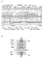
도 1a 및 도 1b는 반도체 장치의 단면도 및 평면도.
도 2a 내지 도 2d는 반도체 장치의 제작 공정에 따른 단면도.
도 3a 내지 도 3d는 반도체 장치의 제작 공정에 따른 단면도.
도 4a 내지 도 4d는 반도체 장치의 제작 공정에 따른 단면도.
도 5a 내지 도 5c는 반도체 장치의 제작 공정에 따른 단면도.
도 6a 및 도 6b는 반도체 장치의 단면도 및 평면도.
도 7a 및 도 7b는 반도체 장치의 단면도 및 평면도.
도 8a 내지 도 8h는 반도체 장치의 제작에 사용하는 반도체 기판의 제작 공정에 따른 단면도.
도 9a 내지 도 9e는 반도체 장치의 제작 공정에 따른 단면도.
도 10a 및 도 10b는 반도체 장치의 단면도 및 평면도.
도 11a 및 도 11b는 반도체 장치의 단면도 및 평면도.
도 12a 내지 도 12f는 반도체 장치의 제작 공정에 따른 단면도.
도 13a 내지 도 13c는 반도체 장치의 회로도.
도 14는 반도체 장치의 회로도.
도 15는 타이밍 차트의 도면.
도 16은 반도체 장치의 회로도.
도 17은 타이밍 차트의 도면.
도 18a 내지 도 18f는 반도체 장치를 사용한 전자 기기를 설명하기 위한 도면.1A and 1B are a cross-sectional view and a plan view of a semiconductor device;
2A to 2D are cross-sectional views of a semiconductor device according to a fabrication process thereof.
3A to 3D are cross-sectional views of a semiconductor device according to a fabrication process thereof.
4A to 4D are cross-sectional views of a semiconductor device according to a fabrication process thereof.
5A to 5C are cross-sectional views of a semiconductor device according to a fabrication process thereof.
6A and 6B are a cross-sectional view and a plan view of a semiconductor device;
7A and 7B are a cross-sectional view and a plan view of a semiconductor device;
8A to 8H are cross-sectional views of a semiconductor substrate used for fabricating a semiconductor device according to a manufacturing process thereof.
9A to 9E are cross-sectional views of the semiconductor device according to the fabrication steps thereof;
10A and 10B are a cross-sectional view and a plan view of a semiconductor device.
11A and 11B are a cross-sectional view and a plan view of a semiconductor device;
12A to 12F are cross-sectional views of a semiconductor device according to a fabrication process thereof;
13A to 13C are circuit diagrams of a semiconductor device.
14 is a circuit diagram of a semiconductor device.
15 is a view of a timing chart;
16 is a circuit diagram of a semiconductor device.
17 is a view of a timing chart.
18A to 18F are diagrams for explaining an electronic apparatus using a semiconductor device.
본 발명의 실시형태의 일례에 대해서 도면을 사용하여 이하에 설명한다. 다만, 본 발명은 이하의 설명에 한정되지 않고, 본 발명의 형태 및 상세한 사항은 본 발명의 취지 및 범위에서 벗어남이 없이 다양하게 변경될 수 있다는 것은 당업자라면 용이하게 이해할 수 있다. 따라서, 본 발명은 이하의 실시형태의 기재 내용에 한정하여 해석되는 것은 아니다.An embodiment of the present invention will be described below with reference to the drawings. It is to be understood, however, that the present invention is not limited to the following description, and that various changes and modifications may be made therein without departing from the spirit and scope of the invention. Therefore, the present invention is not construed as being limited to the description of the following embodiments.
또한, 도면 등에서 나타내는 각 구성의 위치, 크기, 범위 등은 이해를 용이하게 하기 위해서 실제의 위치, 크기, 범위 등을 나타내지 않는 경우가 있다. 따라서, 개시하는 발명은 반드시 도면 등에 개시된 위치, 크기, 범위 등에 한정되지 않는다.In addition, the position, size, range, and the like of each structure shown in the drawings and the like may not show the actual position, size, range and the like in order to facilitate understanding. Therefore, the disclosed invention is not necessarily limited to the position, size, range and the like disclosed in the drawings and the like.
또한, 본 명세서 등에 있어서의 “제 1”, “제 2”, “제 3” 등의 서수사(序數詞)는, 구성 요소의 혼동을 회피하기 위해서 붙이는 것이며, 수(數)적으로 한정하는 것은 아닌 것을 부기한다.The ordinal numbers such as "first", "second", "third", etc. in the present specification are added in order to avoid confusion of the constituent elements, It is not.
(실시형태 1)(Embodiment 1)
본 실시형태에서는, 본 발명의 일 형태에 따른 반도체 장치의 구성 및 그 제작 방법에 대해서 도 1a 내지 도 6b를 참조하여 설명한다.In the present embodiment, a structure of a semiconductor device and a manufacturing method thereof according to an embodiment of the present invention will be described with reference to Figs. 1A to 6B.
<반도체 장치의 단면 구성 및 평면 구성><Sectional and Planar Configuration of Semiconductor Device>
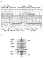
도 1a 및 도 1b는, 반도체 장치의 구성의 일례이다. 도 1a에는, 반도체 장치의 단면을 도시하고, 도 1b에는 반도체 장치의 평면을 도시한다. 여기서, 도 1a는 도 1b의 A1-A2 및 B1-B2에 있어서의 단면에 상당한다. 도 1a 및 도 1b에 도시하는 반도체 장치는, 하부(下部)에 제 1 반도체 재료를 사용한 트랜지스터(160)를 갖고, 상부(上部)에 제 2 반도체 재료를 사용한 트랜지스터(162)를 갖는다. 여기서, 제 1 반도체 재료와 제 2 반도체 재료는 상이한 재료로 하는 것이 바람직하다. 예를 들어, 제 1 반도체 재료를 산화물 반도체 이외의 반도체 재료로 하고, 제 2 반도체 재료를 산화물 반도체로 할 수 있다. 산화물 반도체 이외의 반도체 재료로서는, 예를 들어 실리콘, 게르마늄, 실리콘게르마늄, 탄화실리콘, 인듐인, 또는 갈륨비소 등을 사용할 수 있고, 단결정 반도체를 사용하는 것이 바람직하다. 이와 같은 반도체 재료를 사용한 트랜지스터는, 고속 동작이 용이하다. 한편, 산화물 반도체를 사용한 트랜지스터는, 그 특성 때문에, 전하를 장시간 동안 유지할 수 있다.1A and 1B are an example of a configuration of a semiconductor device. Fig. 1A shows a cross section of a semiconductor device, and Fig. 1B shows a plane of a semiconductor device. Here, Fig. 1A corresponds to a cross section taken along the line A1-A2 and B1-B2 in Fig. 1B. The semiconductor device shown in Figs. 1A and 1B has a
또한, 상기 트랜지스터 중 양쪽 모두는 n채널형 트랜지스터로서 설명하지만, p채널형 트랜지스터를 사용할 수 있는 것은 물론이다. 또한, 개시하는 발명의 기술적인 본질은, 정보를 유지하기 위해서 산화물 반도체와 같은 오프 전류를 충분히 저감시킬 수 있는 반도체 재료를 트랜지스터(162)에 사용하는 점에 있기 때문에, 반도체 장치에 사용되는 재료나 반도체 장치의 구조 등, 반도체 장치의 구체적인 구성은 여기서 나타내는 구성에 한정될 필요는 없다.Although both of the transistors are described as n-channel transistors, it goes without saying that p-channel transistors can be used. The technical nature of the disclosed invention is that the
도 1a 및 도 1b에 도시하는 트랜지스터(160)는, 반도체 재료(예를 들어, 실리콘 등)를 포함하는 기판(100)에 형성된 채널 형성 영역(116)과, 채널 형성 영역(116)을 끼우도록 형성된 불순물 영역(120)과, 불순물 영역(120)에 접하는 금속 화합물 영역(124)과, 채널 형성 영역(116) 위에 형성된 게이트 절연층(108)과, 게이트 절연층(108) 위에 형성된 게이트 전극(110)을 갖는다. 또한, 본 발명의 도면에 있어서, 명시적(明示的)으로는 소스 전극이나 드레인 전극을 갖지 않는 경우가 있지만, 편의상, 이와 같은 상태를 포함하여 트랜지스터라고 부르는 경우가 있다. 또한, 이 경우, 이와 같은 트랜지스터의 접속 관계를 설명하기 위해서 그 트랜지스터의 소스 전극이나 드레인 전극을 본 명세서에 나타내는 경우가 있다.The
트랜지스터(160)의 금속 화합물 영역(124)의 일부에는, 전극(126)이 접속된다. 여기서, 전극(126)은 트랜지스터(160)의 소스 전극이나 드레인 전극으로서 기능한다. 또한, 기판(100) 위에는 트랜지스터(160)를 둘러싸도록 소자 분리 절연층(106)이 형성되고, 트랜지스터(160)에 접하여 절연층(128)이 형성된다. 또한, 고집적화를 실현하기 위해서는, 도 1a 및 도 1b에 도시하는 바와 같이, 트랜지스터(160)가 사이드 월 절연층을 갖지 않는 구성으로 하는 것이 바람직하다. 한편, 트랜지스터(160)의 특성을 중요시하는 경우에는, 게이트 전극(110)의 측면에 사이드 월 절연층을 형성하고, 그 사이드 월 절연층과 중첩하는 영역에 형성된 불순물 농도가 상이한 영역을 포함하여 불순물 영역(120)을 형성하여도 좋다.An
도 1a 및 도 1b에 있어서의 트랜지스터(162)는, 절연층(128) 위에 형성된 소스 전극 또는 드레인 전극(142a), 및 소스 전극 또는 드레인 전극(142b)과, 소스 전극 또는 드레인 전극(142a), 및 소스 전극 또는 드레인 전극(142b)과 전기적으로 접속되는 산화물 반도체층(144)과, 소스 전극 또는 드레인 전극(142a), 소스 전극 또는 드레인 전극(142b), 산화물 반도체층(144)을 덮는 게이트 절연층(146)과, 게이트 절연층(146) 위에 산화물 반도체층(144)과 중첩하도록 형성된 게이트 전극(148a)을 갖는다.1A and 1B includes a source electrode or a
여기서, 산화물 반도체층(144)은 수소 등의 불순물이 충분히 제거됨으로써, 또는 충분한 산소가 공급됨으로써, 고순도화된 것이 바람직하다. 구체적으로는, 예를 들어, 산화물 반도체층(144)의 수소 농도는 5×10¹⁹atoms/cm3 이하, 바람직하게는 5×10¹⁸atoms/cm3 이하, 더 바람직하게는 5×10¹⁷atoms/cm3 이하로 한다. 또한, 상술한 산화물 반도체층(144) 중의 수소 농도는, 2차 이온 질량 분석법(SIMS: Secondary Ion Mass Spectroscopy)으로 측정된다. 이와 같이, 수소 농도가 충분히 저감되어 고순도화되고, 충분한 산소가 공급됨으로써 산소 결손(缺損)에 기인하는 에너지 갭 중의 결함 준위가 저감된 산화물 반도체층(144)에서는, 캐리어 농도가 1×10¹²/cm3 미만, 바람직하게는 1×10¹¹/cm3 미만, 더 바람직하게는 1.45×10¹⁰/cm3 미만이 된다. 예를 들어, 실온(25℃)에서의 오프 전류(여기서는 단위 채널 폭(1μm)당의 값)는, 100zA(1zA는 1×10-21A) 이하, 바람직하게는 10zA 이하가 된다. 이와 같이, i형화(진성화) 또는 실질적으로 i형화된 산화물 반도체를 사용함으로써, 매우 뛰어난 오프 전류 특성을 갖는 트랜지스터(162)를 얻을 수 있다.Here, it is preferable that the
도 1a 및 도 1b에 있어서의 용량 소자(164)는, 소스 전극 또는 드레인 전극(142a), 산화물 반도체층(144), 게이트 절연층(146), 절연층(150), 및 전극(149a)으로 구성된다. 즉, 소스 전극 또는 드레인 전극(142a)은 용량 소자(164)의 한쪽의 전극으로서 기능하고, 전극(149a)은 용량 소자(164)의 다른 쪽의 전극으로서 기능한다.1A and 1B includes a source electrode or a
도 1a 및 도 1b에 도시되는 용량 소자(164)에서는, 산화물 반도체층(144)과 게이트 절연층(146) 및 절연층(150)을 적층시킴으로써, 소스 전극 또는 드레인 전극(142a)과 전극(149a) 사이의 절연성을 충분히 확보할 수 있다. 또한, 충분한 용량을 확보하기 위해서 게이트 절연층(146) 및 절연층(150) 중 어느 한쪽을 갖지 않는 구성의 용량 소자(164)를 채용하여도 좋다. 또한, 충분한 용량을 확보하기 위해서 산화물 반도체층(144)을 갖지 않는 구성의 용량 소자(164)를 채용하여도 좋다. 또한, 산화물 반도체층(144)을 갖지 않는 구성의 용량 소자(164)를 채용하여도 좋다.1A and 1B, the
본 실시형태에서는, 트랜지스터(160)와 트랜지스터(162)가 적어도 일부가 중첩하도록 형성된다. 또한, 트랜지스터(162) 및 용량 소자(164)가 트랜지스터(160)와 중첩하도록 형성된다. 예를 들어, 용량 소자(164)의 전극(149a)은 트랜지스터(162)의 게이트 전극(148a)과 적어도 일부가 중첩하여 형성된다. 또한, 용량 소자(164)의 전극(149a)은 트랜지스터(160)의 게이트 전극(110)과 적어도 일부가 중첩하여 형성되는 구성으로 하여도 좋다. 이와 같은 평면 레이아웃을 채용함으로써, 고집적화가 가능하다. 예를 들어, 최소 가공 치수를 F로 하여 메모리 셀이 차지하는 면적을 9F2 내지 25F2로 할 수 있다. 또한, 상기 평면 레이아웃은, 트랜지스터(162)의 게이트 전극(148a)과 용량 소자(164)의 전극(149a)을 상이한 도전층으로 형성하고, 게이트 전극(148a) 위에 트랜지스터(162)를 덮는 절연층(150)을 형성함으로써 실현된다. 전극을 형성하는 프로세스의 제한에 의하여 게이트 전극(148a)과 전극(149a)을 같은 도전층으로 형성하면 전극의 간격이 충분히 좁은 구성으로 하는 것이 어렵다. 이것에 대해서 게이트 전극(148a)과 전극(149a)을 상이한 도전층으로 형성함으로써 이들의 간격을 충분히 좁게 하고 전극의 일부가 중첩하도록 구성하는 것이 가능하게 되기 때문에 고집적화가 가능하게 된다.In the present embodiment, the
또한, 트랜지스터(162) 및 용량 소자(164)에 있어서, 소스 전극 또는 드레인 전극(142a), 및 소스 전극 또는 드레인 전극(142b)의 단부는 테이퍼 형상인 것이 바람직하다. 이 이유는, 소스 전극 또는 드레인 전극(142a), 소스 전극 또는 드레인 전극(142b)의 단부를 테이퍼 형상으로 함으로써, 산화물 반도체층(144)의 피복성을 향상시켜, 단절(斷切)을 방지할 수 있기 때문이다. 여기서, 테이퍼 각은 예를 들어 30° 이상 60° 이하로 한다. 또한, 테이퍼 각이란, 테이퍼 형상을 갖는 층(예를 들어, 소스 전극 또는 드레인 전극(142a))을 그 단면(기판의 표면과 직교하는 면)에 수직인 방향으로부터 관찰하였을 때에, 상기 층의 측면과 저면(底面)이 이루는 경사 각도를 가리킨다.In the
게이트 전극(148a)을 덮도록 절연층(150)이 형성되고, 트랜지스터(162) 및 용량 소자(164) 위에는, 절연층(151)이 형성되고, 절연층(151) 위에는 절연층(152)이 형성된다. 그리고, 게이트 절연층(146), 절연층(150), 절연층(151), 절연층(152) 등에 형성된 개구에는 전극(154)이 형성되고, 절연층(152) 위에는 전극(154)과 접속하는 배선(156)이 형성된다. 또한, 도 1a 및 도 1b에서는, 전극(126) 및 전극(154)을 사용하여 금속 화합물 영역(124), 소스 전극 또는 드레인 전극(142b), 및 배선(156)을 접속하지만, 개시하는 발명은 이것에 한정되지 않는다. 예를 들어, 소스 전극 또는 드레인 전극(142b)을 금속 화합물 영역(124)에 직접 접촉시켜도 좋다. 또는, 배선(156)을 소스 전극 또는 드레인 전극(142b)에 직접 접촉시켜도 좋다.An insulating
또한, 도 1a 및 도 1b에 있어서, 금속 화합물 영역(124)과 소스 전극 또는 드레인 전극(142b)을 접속하는 전극(126)과, 소스 전극 또는 드레인 전극(142b)과 배선(156)을 접속하는 전극(154)은 중첩하여 배치된다. 즉, 트랜지스터(160)의 소스 전극 또는 드레인 전극으로서 기능하는 전극(126)과, 트랜지스터(162)의 소스 전극 또는 드레인 전극(142b)이 접하는 영역은, 트랜지스터(162)의 소스 전극 또는 드레인 전극(142b)과, 메모리 셀 중의 하나와 다른 메모리 셀을 접속하는 배선(156)이 접하는 영역과 중첩된다. 이와 같은 레이아웃을 채용함으로써, 고집적화를 도모할 수 있다.1A and 1B, the
<반도체 장치의 제작 방법><Manufacturing Method of Semiconductor Device>
다음에, 상기 반도체 장치의 제작 방법의 일례에 대해서 설명한다. 이하에서는, 먼저 하부 트랜지스터(160)의 제작 방법에 대해서 도 2a 내지 도 3d를 참조하여 설명하고, 그 후 상부 트랜지스터(162) 및 용량 소자(164)의 제작 방법에 대해서 도 4a 내지 도 5c를 참조하여 설명한다.Next, an example of a manufacturing method of the semiconductor device will be described. Hereinafter, a method of manufacturing the
<하부 트랜지스터의 제작 방법>≪ Method of fabricating lower transistor &
우선, 반도체 재료를 포함하는 기판(100)을 준비한다(도 2a 참조). 반도체 재료를 포함하는 기판(100)으로서는, 실리콘이나 탄화실리콘 등의 단결정 반도체 기판, 다결정 반도체 기판, 실리콘 게르마늄 등의 화합물 반도체 기판, SOI 기판 등을 적용할 수 있다. 여기서는, 반도체 재료를 포함하는 기판(100)으로서, 단결정 실리콘 기판을 사용하는 경우의 일례에 대해서 나타낸다. 또한, 일반적으로는 “SOI 기판”은, 절연 표면 위에 실리콘 반도체층이 형성된 구성의 기판을 말하지만, 본 명세서 등에 있어서의 개념으로서는, 절연 표면 위에 실리콘 이외의 재료로 이루어지는 반도체층이 형성된 구성의 기판도 포함한다. 즉, “SOI 기판”이 갖는 반도체층은, 실리콘 반도체층에 한정되지 않는다. 또한, SOI 기판에는, 유리 기판 등의 절연 기판 위에 절연층을 개재하여 반도체층이 형성된 구성이 포함된다.First, a
또한, 반도체 재료를 포함하는 기판(100)으로서, 실리콘 등의 단결정 반도체 기판을 사용하면, 반도체 장치의 판독 동작을 고속화할 수 있기 때문에 특히 적합하다.In addition, when a single crystal semiconductor substrate such as silicon is used as the
기판(100) 위에는, 소자 분리 절연층을 형성하기 위한 마스크가 되는 보호층(102)을 형성한다(도 2a 참조). 보호층(102)으로서는, 예를 들어, 산화실리콘이나 질화실리콘, 산화질화실리콘 등을 재료로 하는 절연층을 사용할 수 있다. 또한, 이 공정의 전후(前後)에 있어서, 트랜지스터의 임계값 전압을 제어하기 위해서, n형의 도전성을 부여하는 불순물 원소나 p형의 도전성을 부여하는 불순물 원소를 기판(100)에 첨가하여도 좋다. 반도체가 실리콘인 경우, n형의 도전성을 부여하는 불순물 원소로서는, 예를 들어, 인이나 비소 등을 사용할 수 있다. 또한, p형의 도전성을 부여하는 불순물 원소로서는, 예를 들어 붕소, 알루미늄, 갈륨 등을 사용할 수 있다.On the
다음에, 상기 보호층(102)을 마스크로 하여 에칭을 행하고, 보호층(102)으로 덮이지 않는 영역(노출되는 영역) 중의 기판(100)의 일부를 제거한다. 이로써, 다른 반도체 영역과 분리된 반도체 영역(104)이 형성된다(도 2b 참조). 상기 에칭에는, 드라이 에칭을 사용하는 것이 바람직하지만, 웨트 에칭을 사용하여도 좋다. 에칭 가스나 에칭 액에 대해서는 피(被)에칭 재료에 따라 적절히 선택할 수 있다.Next, etching is performed using the
다음에, 반도체 영역(104)을 덮도록 절연층을 형성하고, 반도체 영역(104)에 중첩하는 영역의 절연층을 선택적으로 제거함으로써, 소자 분리 절연층(106)을 형성한다(도 2c 참조). 상기 절연층은, 산화실리콘이나 질화실리콘, 산화질화실리콘 등을 사용하여 형성된다. 절연층을 제거하는 방법으로서는, CMP(화학적 기계적 연마) 등의 연마 처리나 에칭 처리 등이 있지만, 그 중에서 어느 처리법을 사용하여도 좋다. 또한, 반도체 영역(104)을 형성한 후, 또는 소자 분리 절연층(106)을 형성한 후에는, 상기 보호층(102)을 제거한다.Next, an insulating layer is formed so as to cover the
여기서, CMP 처리란, 표면을 화학적·기계적인 복합 작용에 의하여 평탄화하는 수법이다. 보다 구체적으로는, 연마 스테이지 위에 연마포를 부착하고, 피가공물과 연마포 사이에 슬러리(연마제)를 공급하면서 연마 스테이지와 피가공물을 각각 회전 또는 요동(搖動)시켜 피가공물의 표면을, 슬러리와 피가공물 표면 사이에서의 화학 반응 및 연마포와 피가공물의 기계적 연마의 작용에 의하여 피가공물의 표면을 연마하는 방법이다.Here, the CMP process is a technique of planarizing the surface by a chemical-mechanical complex action. More specifically, the polishing cloth is attached on the polishing stage, and the polishing stage and the workpiece are respectively rotated or shaken while supplying a slurry (abrasive) between the workpiece and the polishing cloth, The surface of the workpiece is polished by chemical reaction between the surface of the workpiece and mechanical polishing of the polishing cloth and the workpiece.
또한, 소자 분리 절연층(106)의 형성 방법으로서, 절연층을 선택적으로 제거하는 방법 이외에 산소를 주입함으로써 절연성을 갖는 영역을 형성하는 방법 등을 사용할 수도 있다.As a method of forming the element
다음에, 반도체 영역(104) 표면에 절연층을 형성하고, 상기 절연층 위에 도전 재료를 포함하는 층을 형성한다.Next, an insulating layer is formed on the surface of the
절연층은, 이후 게이트 절연층이 되는 층이며, 예를 들어, 반도체 영역(104) 표면의 열 처리(열 산화 처리나 열 질화 처리 등)에 의하여 형성할 수 있다. 열 처리 대신에 고밀도 플라즈마 처리를 적용하여도 좋다. 고밀도 플라즈마 처리는, 예를 들어, 헬륨(He), 아르곤(Ar), 크립톤(Kr), 크세논(Xe) 등의 희 가스, 산소, 산화질소, 암모니아, 질소, 수소 등 중 어느 가스의 혼합 가스를 사용하여 행할 수 있다. 물론, CVD법이나 스퍼터링법 등을 사용하여 절연층을 형성하여도 좋다. 상기 절연층은, 산화갈륨, 산화실리콘, 산화질화실리콘, 질화실리콘, 산화하프늄, 산화알루미늄, 산화탄탈, 산화이트륨, 하프늄실리케이트(HfSixOy(x>0, y>0)), 질소가 첨가된 하프늄실리케이트(HfSixOyNz(x>0, y>0, z>0)), 질소가 첨가된 하프늄알루미네이트(HfAlxOyNz(x>0, y>0, z>0)) 등을 포함하는 단층 구조 또는 적층 구조로 하는 것이 바람직하다. 또한, 절연층의 두께는 예를 들어, 1nm 이상 100nm 이하, 바람직하게는 10nm 이상 50nm 이하로 할 수 있다.The insulating layer is a layer to be a gate insulating layer thereafter. For example, the insulating layer can be formed by heat treatment (thermal oxidation treatment, thermal nitriding treatment, or the like) on the surface of the
도전 재료를 포함하는 층은, 알루미늄이나 구리, 티타늄, 탄탈, 텅스텐 등의 금속 재료를 사용하여 형성할 수 있다. 또한, 다결정 실리콘 등의 반도체 재료를 사용하여 도전 재료를 포함하는 층을 형성하여도 좋다. 형성 방법도 특별히 한정되지 않고, 증착법, CVD법, 스퍼터링법, 스핀코팅법 등의 각종 성막 방법을 사용할 수 있다. 또한, 본 실시형태에서는, 도전 재료를 포함하는 층을 금속 재료를 사용하여 형성하는 경우의 일례에 대해서 나타낸다.The layer containing the conductive material can be formed using a metal material such as aluminum, copper, titanium, tantalum or tungsten. A layer containing a conductive material may be formed using a semiconductor material such as polycrystalline silicon. The forming method is not particularly limited, and various film forming methods such as a vapor deposition method, a CVD method, a sputtering method, and a spin coating method can be used. In this embodiment, an example in which a layer containing a conductive material is formed using a metal material is shown.
그 후, 절연층 및 도전 재료를 포함하는 층을 선택적으로 에칭하여 게이트 절연층(108), 게이트 전극(110)을 형성한다(도 2c 참조).Thereafter, the insulating layer and the layer including the conductive material are selectively etched to form the
다음에, 반도체 영역(104)에 인(P)이나 비소(As) 등을 첨가하여 채널 형성 영역(116) 및 불순물 영역(120)을 형성한다(도 2d 참조). 또한, 여기서는 n형 트랜지스터를 형성하기 위해서 인이나 비소를 첨가하지만, p형 트랜지스터를 형성하는 경우에는, 붕소(B)나 알루미늄(Al) 등의 불순물 원소를 첨가하면 좋다. 여기서, 첨가하는 불순물의 농도는 적절히 설정할 수 있지만, 반도체 소자가 고도로 미세화되는 경우에는, 그 농도를 높이는 것이 바람직하다.Next, phosphorus (P), arsenic (As), or the like is added to the
또한, 게이트 전극(110)의 주위에 사이드 월 절연층을 형성하고, 불순물 원소가 상이한 농도로 첨가된 불순물 영역을 형성하여도 좋다.A sidewall insulating layer may be formed around the
다음에, 게이트 전극(110), 불순물 영역(120) 등을 덮도록 금속층(122)을 형성한다(도 3a 참조). 상기 금속층(122)은, 진공 증착법이나 스퍼터링법, 스핀코팅법 등의 각종 성막 방법을 사용하여 형성할 수 있다. 금속층(122)은 반도체 영역(104)을 구성하는 반도체 재료와 반응함으로써 저저항의 금속 화합물이 되는 금속 재료를 사용하여 형성하는 것이 바람직하다. 이와 같은 금속 재료로서는, 예를 들어 티타늄, 탄탈, 텅스텐, 니켈, 코발트, 백금 등이 있다.Next, a
다음에, 열 처리를 행하여 상기 금속층(122)과 반도체 재료를 반응시킨다. 이로써, 불순물 영역(120)에 접하는 금속 화합물 영역(124)이 형성된다(도 3a 참조). 또한, 게이트 전극(110)으로서 다결정 실리콘 등을 사용하는 경우에는, 게이트 전극(110)의 금속층(122)과 접촉하는 부분에도 금속 화합물 영역이 형성된다.Next, a heat treatment is performed to react the
상기 열 처리로서는, 예를 들어, 플래시 램프 조사에 의한 열 처리를 사용할 수 있다. 물론, 그 이외의 열 처리 방법을 사용하여도 좋지만, 금속 화합물의 형성에 따른 화학 반응의 제어성(制御性)을 향상시키기 위해서는, 극히 단시간의 열 처리를 실현할 수 있는 방법을 사용하는 것이 바람직하다. 또한, 상술한 금속 화합물 영역은, 금속 재료와 반도체 재료의 반응에 의하여 형성되는 것이며, 충분히 도전성이 높아진 영역이다. 상기 금속 화합물 영역을 형성함으로써, 전기 저항을 충분히 저감하고 소자 특성을 향상시킬 수 있다. 또한, 금속 화합물 영역(124)을 형성한 후에는, 금속층(122)은 제거한다.As the heat treatment, for example, heat treatment by flash lamp irradiation can be used. Of course, other heat treatment methods may be used. However, in order to improve the controllability of the chemical reaction due to the formation of the metal compound, it is preferable to use a method capable of realizing an extremely short heat treatment . Further, the above-described metal compound region is formed by the reaction between the metal material and the semiconductor material, and is a region where the conductivity is sufficiently increased. By forming the metal compound region, the electrical resistance can be sufficiently reduced and the device characteristics can be improved. Further, after the
다음에, 금속 화합물 영역(124)의 일부와 접하는 영역에 전극(126)을 형성한다(도 3b 참조). 전극(126)은, 예를 들어 도전 재료를 포함하는 층을 형성한 후에 상기 층을 선택적으로 에칭함으로써 형성된다. 도전 재료를 포함하는 층은, 알루미늄이나 구리, 티타늄, 탄탈, 텅스텐 등의 금속 재료를 사용하여 형성할 수 있다. 또한, 다결정 실리콘 등의 반도체 재료를 사용하여 도전 재료를 포함하는 층을 형성하여도 좋다. 형성 방법도 특별히 한정되지 않고, 증착법, CVD법, 스퍼터링법, 스핀코팅법 등의 각종 성막 방법을 사용할 수 있다.Next, an
또한, 전극(126)은, 절연층(128)을 형성한 후에, 절연층(128)에 금속 화합물 영역(124)까지 도달하는 개구를 형성하고, 상기 개구를 메우도록 형성할 수도 있다.The
이 경우, 예를 들어, 개구를 포함하는 영역에 PVD법에 의하여 티타늄막을 얇게 형성하고, CVD법에 의하여 질화티타늄막을 얇게 형성한 후에, 개구를 메우도록 텅스텐막을 형성하는 방법을 적용할 수 있다. 여기서, PVD법에 의하여 형성되는 티타늄막은, 피형성면의 산화막(자연 산화막 등)을 환원(還元)하고, 하부 전극 등(여기서는 금속 화합물 영역(124))과의 접촉 저항을 저감시키는 기능을 갖는다. 또한, 그 후에 형성되는 질화티타늄막은, 도전성 재료의 확산을 억제하는 배리어 기능을 구비한다. 또한, 티타늄이나 질화티타늄 등에 의한 배리어막을 형성한 후에, 도금법에 의하여 구리 막을 형성하여도 좋다.In this case, for example, a method in which a titanium film is formed thinly by PVD method in an area including an opening, a titanium nitride film is formed thin by a CVD method, and then a tungsten film is formed so as to fill the opening. Here, the titanium film formed by the PVD method has a function of reducing an oxide film (natural oxide film or the like) on the surface to be formed and reducing the contact resistance with the lower electrode or the like (here, the metal compound region 124) . Further, the titanium nitride film formed thereafter has a barrier function for suppressing the diffusion of the conductive material. Alternatively, a copper film may be formed by a plating method after forming a barrier film of titanium or titanium nitride.
다음에, 상술한 공정에 의하여 형성된 각 구성을 덮도록 절연층(128)을 형성한다(도 3c 참조). 절연층(128)은, 산화실리콘, 산화질화실리콘, 질화실리콘, 산화알루미늄 등의 무기 절연 재료를 포함하는 재료를 사용하여 형성할 수 있다. 특히, 절연층(128)에 유전율이 낮은(low-k) 재료를 사용함으로써, 각종 전극이나 배선이 중첩하는 것에 기인하는 용량을 충분히 저감할 수 있기 때문에, 바람직하다. 또한, 절연층(128)에는 이들의 재료를 사용한 다공성(多孔性) 절연층을 적용하여도 좋다. 다공성의 절연층에서는, 밀도가 높은 절연층과 비교하여 유전율이 저하하기 때문에, 전극이나 배선에 기인하는 용량을 더 저감할 수 있다. 또한, 절연층(128)은, 폴리이미드, 아크릴 등의 유기 절연 재료를 사용하여 형성할 수도 있다. 또한, 여기서는 절연층(128)의 단층 구조로 하지만, 개시하는 발명의 일 형태는 이것에 한정되지 않는다. 2층 이상의 적층 구조로 하여도 좋다.Next, an insulating
상술한 공정에 의하여 반도체 재료를 포함하는 기판(100)을 사용한 트랜지스터(160)가 형성된다(도 3c 참조). 이와 같은 트랜지스터(160)는, 고속 동작을 행할 수 있다는 특징을 갖는다. 따라서, 상기 트랜지스터를 판독용의 트랜지스터로서 사용함으로써, 정보의 판독을 고속으로 행할 수 있다.By the above-described process, a
그 후, 트랜지스터(162) 및 용량 소자(164)를 형성하기 전의 처리로서, 절연층(128)에 CMP 처리를 행하여 게이트 전극(110) 및 전극(126)의 상면을 노출시킨다(도 3d 참조). 게이트 전극(110) 및 전극(126)의 상면을 노출시키는 처리로서는, CMP 처리 이외에 에칭 처리 등을 적용할 수도 있지만, 트랜지스터(162)의 특성을 향상시키기 위해서 절연층(128)의 표면은 가능한 한 평탄하게 해 두는 것이 바람직하다.Thereafter, as a process before the
또한, 상기 각 공정의 전후에는, 전극이나 배선, 반도체층, 절연층 등을 더 형성하는 공정을 포함하여도 좋다. 예를 들어, 배선의 구조로서 절연층 및 도전층의 적층 구조로 이루어지는 다층 배선 구조를 채용하여 고도로 집적화한 반도체 장치를 실현할 수도 있다.Furthermore, before and after each of the above steps, a step of further forming an electrode, a wiring, a semiconductor layer, an insulating layer, and the like may be included. For example, a highly integrated semiconductor device can be realized by employing a multilayer wiring structure having a multilayer structure of an insulating layer and a conductive layer as a wiring structure.
<상부 트랜지스터의 제작 방법>≪ Manufacturing method of upper transistor &
다음에, 게이트 전극(110), 전극(126), 절연층(128) 등의 위에 도전층을 형성하고, 상기 도전층을 선택적으로 에칭하여 소스 전극 또는 드레인 전극(142a), 소스 전극 또는 드레인 전극(142b)을 형성한다(도 4a 참조).Next, a conductive layer is formed on the
도전층은, 스퍼터링법을 비롯한 PVD법이나, 플라즈마 CVD법 등의 CVD법을 사용하여 형성할 수 있다. 또한, 도전층의 재료로서는, 알루미늄, 크롬, 구리, 탄탈, 티타늄, 몰리브덴, 텅스텐 중에서 선택된 원소나, 상술한 원소를 성분으로 하는 합금 등을 사용할 수 있다. 망간, 마그네슘, 지르코늄, 베릴륨, 네오디뮴, 스칸듐 중 어느 하나, 또는 이들을 복수 조합한 재료를 사용하여도 좋다.The conductive layer can be formed by a CVD method such as a PVD method or a plasma CVD method including a sputtering method. As the material of the conductive layer, a material selected from among aluminum, chromium, copper, tantalum, titanium, molybdenum, and tungsten, an alloy containing the above-described elements as a component, and the like can be used. Manganese, magnesium, zirconium, beryllium, neodymium, or scandium, or a combination of these materials may be used.
도전층은, 단층 구조라도 좋고, 2층 이상의 적층 구조로 하여도 좋다. 예를 들어, 티타늄막이나 질화티타늄막의 단층 구조, 실리콘을 포함하는 알루미늄막의 단층 구조, 알루미늄막 위에 티타늄막이 적층된 2층 구조, 질화티타늄막 위에 티타늄막이 적층된 2층 구조, 티타늄막과 알루미늄막과 티타늄막이 적층된 3층 구조 등을 들 수 있다. 또한, 도전층을 티타늄막이나 질화티타늄막의 단층 구조로 하는 경우에는, 테이퍼 형상을 갖는 소스 전극 또는 드레인 전극(142a), 및 소스 전극 또는 드레인 전극(142b)으로 가공하기 쉽다는 장점이 있다.The conductive layer may have a single-layer structure or a laminated structure of two or more layers. For example, a single-layer structure of a titanium film or a titanium nitride film, a single-layer structure of an aluminum film containing silicon, a two-layer structure in which a titanium film is laminated on an aluminum film, a two-layer structure in which a titanium film is laminated on a titanium nitride film, And a three-layer structure in which a titanium film is laminated. When the conductive layer has a single-layer structure of a titanium film or a titanium nitride film, there is an advantage that it can be easily processed into a tapered source electrode or
또한, 도전층은 도전성의 금속 산화물을 사용하여 형성하여도 좋다. 도전성의 금속 산화물로서는, 산화인듐(In2O3), 산화주석(SnO2), 산화아연(ZnO), 산화인듐산화주석합금(In2O3-SnO2, ITO라고 약기하는 경우가 있다), 산화인듐산화아연합금(In2O3-ZnO), 또는 이들의 금속 산화물 재료에 실리콘 또는 산화실리콘을 함유시킨 것을 사용할 수 있다.The conductive layer may be formed using a conductive metal oxide. Examples of the conductive metal oxide include indium oxide (In2 O3 ), tin oxide (SnO2 ), zinc oxide (ZnO), indium oxide tin oxide alloy (In2 O3 -SnO2 , , Indium oxide-zinc oxide alloy (In2 O3 -ZnO), or a metal oxide material thereof containing silicon or silicon oxide can be used.
도전층의 에칭은, 형성되는 소스 전극 또는 드레인 전극(142a), 및 소스 전극 또는 드레인 전극(142b)의 단부가, 테이퍼 형상이 되도록 행하는 것이 바람직하다. 여기서, 테이퍼 각은, 예를 들어 30° 이상 60° 이하인 것이 바람직하다. 소스 전극 또는 드레인 전극(142a), 소스 전극 또는 드레인 전극(142b)의 단부를 테이퍼 형상이 되도록 에칭함으로써, 이후 형성되는 게이트 절연층(146)의 피복성을 향상시켜 단절을 방지할 수 있다.The etching of the conductive layer is preferably performed such that the end portions of the source electrode or the
상부 트랜지스터의 채널 길이(L)는, 소스 전극 또는 드레인 전극(142a), 및 소스 전극 또는 드레인 전극(142b) 하단부(下端部)의 간격에 따라 결정된다. 또한, 채널 길이(L)가 25nm 미만의 트랜지스터를 형성하는 경우에 사용하는 마스크를 형성하기 위한 노광을 행할 때에는, 수nm 내지 수십nm의 파장이 짧은 초자외선(Extreme Ultraviolet)을 사용하는 것이 바람직하다. 초자외선에 의한 노광은, 해상도가 높고, 초점(焦點)심도도 크다. 따라서, 이후 형성되는 트랜지스터의 채널 길이(L)를 10nm 이상 1000nm(1μm) 이하로 할 수도 있고, 회로의 동작 속도를 높일 수 있다. 또한, 미세화에 의하여 반도체 장치의 소비 전력을 저감할 수도 있다.The channel length L of the upper transistor is determined according to the interval between the source electrode or the
또한, 절연층(128) 위에는, 하지로서 기능하는 절연층을 형성하여도 좋다. 상기 절연층은, PVD법이나 CVD법 등을 사용하여 형성할 수 있다.An insulating layer functioning as a base may be formed on the insulating
또한, 소스 전극 또는 드레인 전극(142a), 및 소스 전극 또는 드레인 전극(142b) 위에 각각 절연층을 형성하여도 좋다. 절연층은 이후 형성되는 게이트 전극의 일부와 중첩하도록 형성된다. 이와 같은 절연층을 형성함으로써, 게이트 전극과, 소스 전극 또는 드레인 전극 사이의 용량을 저감시킬 수 있다.An insulating layer may be formed over the source or
다음에, 소스 전극 또는 드레인 전극(142a), 및 소스 전극 또는 드레인 전극(142b)을 덮도록 산화물 반도체층을 형성한 후, 상기 산화물 반도체층을 선택적으로 에칭하여 산화물 반도체층(144)을 형성한다(도 4b 참조).Next, an oxide semiconductor layer is formed so as to cover the source or
산화물 반도체층으로서는, 적어도 In, Ga, Sn, 및 Zn으로부터 선택된 1종 이상의 원소를 함유한다. 예를 들어, 4원계 금속 산화물인 In-Sn-Ga-Zn-O계나, 3원계 금속 산화물인 In-Ga-Zn-O계, In-Sn-Zn-O계, In-Al-Zn-O계, Sn-Ga-Zn-O계, Al-Ga-Zn-O계, Sn-Al-Zn-O계나, 2원계 금속 산화물인 In-Zn-O계, In-Ga-O계, Sn-Zn-O계, Al-Zn-O계, Zn-Mg-O계, Sn-Mg-O계, In-Mg-O계나, In-O계, Sn-O계, Zn-O계 등을 사용하여 형성할 수 있다. 또한, 상기 산화물 반도체에 In, Ga, Sn, 및 Zn 이외의 원소, 예를 들어 SiO2를 포함시켜도 좋다.The oxide semiconductor layer contains at least one element selected from at least In, Ga, Sn, and Zn. In-Sn-Zn-O, In-Sn-Zn-O, In-Sn-Zn-O, In-Zn-O-based, In-Ga-O-based, Sn-Al-Zn-O based, Sn-Al-Zn-O based, Zn-O type, Al-Zn-O type, Zn-Mg-O type, Sn-Mg-O type, In-Mg-O type, In-O type, Sn-O type and Zn-O type . In addition, the oxide semiconductor may contain an element other than In, Ga, Sn, and Zn, for example, SiO2 .
예를 들어, In-Ga-Zn-O계 산화물 반도체는, 인듐(In), 갈륨(Ga), 아연(Zn)을 갖는 산화물 반도체를 의미하고, 그 조성 비율은 불문하다.For example, the In-Ga-Zn-O-based oxide semiconductor means an oxide semiconductor having indium (In), gallium (Ga), and zinc (Zn), and the composition ratio thereof is not limited.
그 중에서도, In-Ga-Zn-O계 산화물 반도체 재료는, 무전계일 때의 저항이 충분히 높고, 오프 전류를 충분히 작게 할 수 있고, 또한, 전계 효과 이동도도 높기 때문에, 반도체 장치에 사용하는 반도체 재료로서는 적합하다.In particular, the In-Ga-Zn-O-based oxide semiconductor material has a sufficiently high resistance in the electroless state, a sufficiently low off current, and a high field effect mobility, It is suitable as a material.
In-Ga-Zn-O계 산화물 반도체 재료의 대표적인 예로서는, InGaO3(ZnO)m(m>0)으로 표기되는 것이 있다. 또한, Ga 대신에 M의 표기를 사용하여 InMO3(ZnO)m(m>0)으로 표기되는 산화물 반도체 재료가 있다. 여기서, M은 갈륨(Ga), 알루미늄(Al), 철(Fe), 니켈(Ni), 망간(Mn), 코발트(Co) 등 중에서 선택된 하나의 금속 원소 또는 복수의 금속 원소를 나타낸다. 예를 들어, M으로서는, Ga, Ga 및 Al, Ga 및 Fe, Ga 및 Ni, Ga 및 Mn, Ga 및 Co 등을 적용할 수 있다. 또한, 상술한 조성은 결정 구조로부터 얻을 수 있는 조성이고, 어디까지나 일례에 불과한 것을 부기한다.A typical example of the In-Ga-Zn-O-based oxide semiconductor material is expressed by InGaO3 (ZnO)m (m> 0). Further, there is an oxide semiconductor material represented by InMO3 (ZnO)m (m > 0) by using the notation of M instead of Ga. Here, M represents one metal element or a plurality of metal elements selected from gallium (Ga), aluminum (Al), iron (Fe), nickel (Ni), manganese (Mn), cobalt (Co) For example, Ga, Ga and Al, Ga and Fe, Ga and Ni, Ga and Mn, Ga and Co and the like can be applied as M. It should be noted that the above-mentioned composition is a composition obtainable from the crystal structure, and is merely an example.
산화물 반도체층을 스퍼터링법에 의하여 제작하기 위한 타깃으로서는, In:Ga:Zn=1:x:y(x는 0 이상, y는 0.5 이상 5 이하)의 조성 비율로 나타내는 것을 사용하는 것이 바람직하다. 예를 들어, In2O3:Ga2O3:ZnO=1:1:2[mol수 비율]의 조성 비율을 갖는 금속 산화물 타깃 등을 사용할 수 있다. 또한, In2O3:Ga2O3:ZnO=1:1:1[mol수 비율]의 조성 비율을 갖는 금속 산화물 타깃이나 In2O3:Ga2O3:ZnO=1:1:4[mol수 비율]의 조성 비율을 갖는 금속 산화물 타깃이나 In2O3:Ga2O3:ZnO=1:0:2[mol수 비율]의 조성 비율을 갖는 금속 산화물 타깃을 사용할 수도 있다.As a target for forming the oxide semiconductor layer by the sputtering method, it is preferable to use a material represented by a composition ratio of In: Ga: Zn = 1: x: y (x is 0 or more and y is 0.5 or more and 5 or less). For example, a metal oxide target having a composition ratio of In2 O3 : Ga2 O3 : ZnO = 1: 1: 2 [number of moles] can be used. In addition, a metal oxide target having a composition ratio of In2 O3 : Ga2 O3 : ZnO = 1: 1: 1 [molar ratio] or In2 O3 : Ga2 O3 : ZnO = 1: 1: 4 [mol ratio] or a metal oxide target having a composition ratio of in2 O3: Ga 2 O 3: ZnO = 1: 0: 2 is also possible to use a metal oxide target having a composition ratio [mol ratio].
또한, 산화물 반도체로서 In-Zn-O계의 재료를 사용하는 경우, 사용하는 타깃의 조성 비율은 원자수 비율로 In:Zn=50:1 내지 1:2(mol수 비율로 환산하면 In2O3:ZnO=25:1 내지 1:4), 바람직하게는 In:Zn=20:1 내지 1:1(mol수 비율로 환산하면 In2O3:ZnO=10:1 내지 1:2), 더 바람직하게는, In:Zn=15:1 내지 1.5:1(mol수 비율로 환산하면 In2O3:ZnO=15:2 내지 3:4)로 한다. 예를 들어, In-Zn-O계 산화물 반도체의 형성에 사용되는 타깃은 원자수 비율이 In:Zn:O=X:Y:Z일 때, Z>1.5X+Y로 한다.Further, the oxide When using a material of the type In-Zn-O as a semiconductor, the composition ratio of the target to be used is as a percentage of atoms In: Zn = 50: 1 to 1: in terms of 2 (mol ratio In2 O3: ZnO = 25: 1 to 1: 4), preferably, in: Zn = 20: 1 to 1: 1 (when converted into the mol number ratio ofin 2 O 3: ZnO = 10 : 1 to 1: 2), More preferably, In: Zn = 15: 1 to 1.5: 1 (In2 O3 : ZnO = 15: 2 to 3: 4 in terms of molar ratio). For example, the target used for forming the In-Zn-O-based oxide semiconductor is set to be Z> 1.5X + Y when the atomic ratio is In: Zn: O = X: Y:
본 실시형태에서는, 비정질 구조의 산화물 반도체층을 In-Ga-Zn-O계의 금속 산화물 타깃을 사용하는 스퍼터링법에 의하여 형성한다.In this embodiment mode, an oxide semiconductor layer of an amorphous structure is formed by a sputtering method using a metal oxide target of In-Ga-Zn-O system.
금속 산화물 타깃 중의 금속 산화물의 상대 밀도는 80% 이상, 바람직하게는 95% 이상, 더 바람직하게는 99.9% 이상이다. 상대 밀도가 높은 금속 산화물 타깃을 사용함으로써, 치밀한 구조의 산화물 반도체층을 형성할 수 있다.The relative density of the metal oxide in the metal oxide target is 80% or more, preferably 95% or more, and more preferably 99.9% or more. By using a metal oxide target having a high relative density, a dense oxide semiconductor layer can be formed.
산화물 반도체층을 형성하는 분위기는, 희 가스(대표적으로는 아르곤) 분위기, 산소 분위기, 또는 희 가스(대표적으로는 아르곤)와 산소의 혼합 분위기로 하는 것이 바람직하다. 구체적으로는, 예를 들어, 수소, 물, 수산기, 수소화물 등의 불순물이 1ppm 이하(바람직하게는 10ppb 이하)까지 제거된 고순도 가스 분위기를 사용하는 것이 바람직하다.The atmosphere for forming the oxide semiconductor layer is preferably a rare gas (typically argon) atmosphere, an oxygen atmosphere, or a mixed atmosphere of a rare gas (typically argon) and oxygen. Concretely, it is preferable to use a high-purity gas atmosphere in which impurities such as hydrogen, water, hydroxyl groups, and hydrides are removed to 1 ppm or less (preferably 10 ppb or less).
산화물 반도체층을 형성할 때에는, 예를 들어 감압 상태로 유지된 처리실 내에 피처리물을 유지하고, 피처리물의 온도가 100℃ 이상 550℃ 미만, 바람직하게는 200℃ 이상 400℃ 이하가 되도록 피처리물을 가열한다. 또는, 산화물 반도체층을 형성할 때의 피처리물의 온도는, 실온(25℃±10℃, 15℃ 이상 35℃ 이하)으로 하여도 좋다. 그리고, 처리실 내의 수분을 제거하면서, 수소나 물 등이 제거된 스퍼터링 가스를 도입하고 상기 타깃을 사용하여 산화물 반도체층을 형성한다. 피처리물을 가열하면서 산화물 반도체층을 형성함으로써, 산화물 반도체층에 포함되는 불순물을 저감시킬 수 있다. 또한, 스퍼터링에 의한 손상을 경감시킬 수 있다. 처리실 내의 수분을 제거하기 위해서는, 흡착형의 진공 펌프를 사용하는 것이 바람직하다. 예를 들어, 클라이오 펌프(cryopump), 이온 펌프, 티타늄 서블리메이션 펌프(titanium sublimation pump) 등을 사용할 수 있다. 또한, 터보(turbo) 분자 펌프에 콜드 트랩(cold trap)을 설치한 것을 사용하여도 좋다. 클라이오 펌프 등을 사용하여 배기함으로써, 처리실로부터 수소나 물 등을 제거할 수 있기 때문에, 산화물 반도체층 중의 불순물 농도를 저감할 수 있다.When the oxide semiconductor layer is formed, for example, the object to be processed is held in a treatment chamber kept in a reduced pressure state, and the material to be treated is treated so that the temperature of the substance to be treated is in the range of 100 ° C to 550 ° C, preferably 200 ° C to 400 ° C Heat the water. Alternatively, the temperature of the object to be processed at the time of forming the oxide semiconductor layer may be room temperature (25 占 폚 占 10 占 폚, 15 占 폚 or more and 35 占 폚 or less). Then, while removing moisture in the treatment chamber, sputtering gas from which hydrogen or water is removed is introduced and an oxide semiconductor layer is formed using the target. Impurities contained in the oxide semiconductor layer can be reduced by forming the oxide semiconductor layer while heating the object to be processed. In addition, damage caused by sputtering can be reduced. In order to remove moisture in the treatment chamber, it is preferable to use an adsorption type vacuum pump. For example, a cryopump, an ion pump, a titanium sublimation pump, or the like can be used. Further, a turbo molecular pump having a cold trap may be used. By using a cryo pump or the like to evacuate, hydrogen, water or the like can be removed from the treatment chamber, so that the impurity concentration in the oxide semiconductor layer can be reduced.
산화물 반도체층의 형성 조건으로서는, 예를 들어 피처리물과 타깃의 거리가 170mm, 압력이 0.4Pa, 직류(DC) 전력이 0.5kW, 분위기가 산소(산소 100%) 분위기, 또는 아르곤(아르곤 100%) 분위기, 또는 산소와 아르곤의 혼합 분위기라는 조건을 적용할 수 있다. 또한, 펄스 직류(DC) 전원을 사용하면, 성막시에 형성되는 분말 상태 물질(파티클(particle)이나 먼지라고도 한다)을 저감할 수 있고, 막 두께 분포도 균일하게 되기 때문에 바람직하다. 산화물 반도체층의 두께는, 1nm 이상 50nm 이하, 바람직하게는 1nm 이상 30nm 이하, 더 바람직하게는 1nm 이상 10nm 이하로 한다. 이와 같은 두께의 산화물 반도체층을 사용함으로써, 미세화에 따른 단 채널 효과를 억제할 수 있다. 다만, 적용하는 산화물 반도체 재료나 반도체 장치의 용도 등의 조건에 따라 산화물 반도체층의 적절한 두께는 상이하기 때문에, 그 두께는 사용하는 재료나 용도 등에 따라 선택할 수도 있다.As the conditions for forming the oxide semiconductor layer, for example, the distance between the target and the target is 170 mm, the pressure is 0.4 Pa, the direct current (DC) power is 0.5 kW, the atmosphere is oxygen (100% oxygen) %) Atmosphere, or a mixed atmosphere of oxygen and argon. The use of a pulsed direct current (DC) power supply is preferable because the powder state material (also referred to as particles or dust) formed at the time of film formation can be reduced and the film thickness distribution becomes uniform. The thickness of the oxide semiconductor layer is set to 1 nm or more and 50 nm or less, preferably 1 nm or more and 30 nm or less, and more preferably 1 nm or more and 10 nm or less. By using the oxide semiconductor layer having such a thickness, the short channel effect due to miniaturization can be suppressed. However, since the appropriate thickness of the oxide semiconductor layer differs depending on conditions such as the application of the oxide semiconductor material and the semiconductor device to be applied, the thickness thereof may be selected depending on the materials and applications to be used.
또한, 산화물 반도체층을 스퍼터링법에 의하여 형성하기 전에는, 아르곤 가스를 도입하여 플라즈마를 발생시키는 역 스퍼터링을 행하고, 산화물 반도체층이 형성되는 표면(예를 들어, 절연층(128) 표면)의 부착물을 제거하는 것이 바람직하다. 여기서, 일반적인 스퍼터링은 스퍼터링 타깃에 이온을 충돌시키는 방법을 가리키지만, 역 스퍼터링은 기판의 처리 표면에 이온을 충돌시킴으로써 그 표면을 개질하는 방법을 말한다. 처리 표면에 이온을 충돌시키는 방법으로서는, 아르곤 분위기하에서 처리 표면 측에 고주파 전압을 인가하여 피처리물 부근에 플라즈마를 생성하는 방법 등이 있다. 또한, 아르곤 분위기 대신에 질소, 헬륨, 산소 등에 의한 분위기를 적용하여도 좋다.Before the oxide semiconductor layer is formed by the sputtering method, reverse sputtering in which argon gas is introduced to generate plasma is performed to form an adherend on the surface (for example, the surface of the insulating layer 128) on which the oxide semiconductor layer is formed It is preferable to remove it. Here, general sputtering refers to a method of impinging ions on a sputtering target, but reverse sputtering refers to a method of modifying the surface of the substrate by impinging ions on the processing surface of the substrate. As a method of impinging ions on a treated surface, there is a method of generating a plasma near the object to be treated by applying a high-frequency voltage to the treated surface side in an argon atmosphere. Instead of the argon atmosphere, an atmosphere of nitrogen, helium, oxygen or the like may be applied.
그 후, 산화물 반도체층에 대해서, 열 처리(제 1 열 처리)를 행하는 것이 바람직하다. 이 제 1 열 처리에 의하여 산화물 반도체층 중의 과잉의 수소(물이나 수산기를 포함한다)를 제거하여 산화물 반도체층의 구조가 가지런하게 하고, 에너지 갭 중의 결함 준위를 저감시킬 수 있다. 제 1 열 처리의 온도는 예를 들어 300℃ 이상 550℃ 미만, 또는 400℃ 이상 500℃ 이하로 한다.Thereafter, the oxide semiconductor layer is preferably subjected to heat treatment (first heat treatment). By this first heat treatment, excessive hydrogen (including water and hydroxyl) in the oxide semiconductor layer can be removed, the structure of the oxide semiconductor layer can be made uniform, and the defect level in the energy gap can be reduced. The temperature of the first heat treatment is set to, for example, not less than 300 ° C and not more than 550 ° C, or not less than 400 ° C and not more than 500 ° C.
열 처리는, 예를 들어 저항 발열체 등을 사용한 전기로에 피처리물을 도입하여 질소 분위기하, 450℃, 1시간의 조건으로 행할 수 있다. 열 처리를 행하는 동안, 산화물 반도체층은 대기에 노출시키지 않고, 물이나 수소가 혼입하지 않도록 한다.The heat treatment can be carried out under a nitrogen atmosphere at 450 DEG C for 1 hour by introducing the article to an electric furnace using, for example, a resistance heating element or the like. During the heat treatment, the oxide semiconductor layer is not exposed to the atmosphere, and water or hydrogen is not mixed.
열 처리 장치는 전기로에 한정되지 않고, 가열된 가스 등의 매체로부터의 열 전도, 또는 열 복사(輻射)에 의하여 피처리물을 가열하는 장치를 사용하여도 좋다. 예를 들어, LRTA(Lamp Rapid Thermal Anneal) 장치, GRTA(Gas Rapid Thermal Anneal) 장치 등의 RTA(Rapid Thermal Anneal) 장치를 사용할 수 있다. LRTA 장치는, 할로겐 램프, 메탈 할라이드 램프, 크세논 아크 램프, 카본 아크 램프, 고압 나트륨 램프, 고압 수은 램프 등의 램프로부터 방출되는 광(전자파)의 복사에 의하여 피처리물을 가열하는 장치이다. GRTA 장치는, 고온의 가스를 사용하여 열 처리를 행하는 장치이다. 가스로서는, 아르곤 등의 희 가스, 또는 질소와 같은 열 처리에 의하여 피처리물과 반응하지 않는 불활성 기체가 사용된다.The heat treatment apparatus is not limited to an electric furnace but may be an apparatus for heating a material to be treated by heat conduction from a medium such as heated gas or by heat radiation. For example, an RTA (Rapid Thermal Anneal) device such as a Lamp Rapid Thermal Anneal (LRTA) device or a GRTA (Gas Rapid Thermal Anneal) device can be used. The LRTA apparatus is an apparatus for heating a material to be irradiated by radiating light (electromagnetic waves) emitted from a lamp such as a halogen lamp, a metal halide lamp, a xenon arc lamp, a carbon arc lamp, a high pressure sodium lamp or a high pressure mercury lamp. The GRTA apparatus is a device for performing heat treatment by using a high-temperature gas. As the gas, a rare gas such as argon or an inert gas which does not react with the object to be treated by heat treatment such as nitrogen is used.
예를 들어, 제 1 열 처리로서, 가열된 불활성 가스 분위기 중에 피처리물을 투입하여 수분간 가열한 후, 상기 불활성 가스 분위기 중에서 피처리물을 꺼내는 GRTA 처리를 행하여도 좋다. GRTA 처리를 사용하면, 단시간에서의 고온 열 처리가 가능하게 된다. 또한, 피처리물의 내열 온도를 초과하는 온도라도 적용할 수 있다. 또한, 처리 중에 불활성 가스를, 산소를 포함하는 가스로 바꾸어도 좋다. 산소를 포함하는 분위기에 있어서, 제 1 열 처리를 행함으로써, 산소 결손에 기인하는 에너지 갭 중의 결함 준위를 저감할 수 있기 때문이다.For example, as the first heat treatment, a GRTA treatment may be performed in which the object to be treated is put in a heated inert gas atmosphere and heated for several minutes, and then the object to be treated is taken out in the inert gas atmosphere. By using the GRTA treatment, high-temperature heat treatment can be performed in a short time. It is also possible to apply a temperature exceeding the heat resistant temperature of the object to be treated. In addition, the inert gas may be changed to a gas containing oxygen during the process. This is because, by performing the first heat treatment in an atmosphere containing oxygen, the defect level in the energy gap due to oxygen deficiency can be reduced.
또한, 불활성 가스 분위기로서는, 질소 또는 희 가스(헬륨, 네온, 아르곤 등)를 주성분으로 하는 분위기이며, 물, 수소 등이 포함되지 않는 분위기를 적용하는 것이 바람직하다. 예를 들어, 열 처리 장치에 도입하는 질소나 헬륨, 네온, 아르곤 등의 희 가스의 순도를 6N(99.9999%) 이상, 바람직하게는 7N(99.99999%) 이상(즉, 불순물 농도가 1ppm 이하, 바람직하게는 0.1ppm 이하)으로 한다.As the inert gas atmosphere, it is preferable to use an atmosphere containing nitrogen or a rare gas (helium, neon, argon, etc.) as a main component and an atmosphere not containing water, hydrogen or the like. For example, the purity of a rare gas such as nitrogen, helium, neon or argon introduced into a heat treatment apparatus is preferably 6N (99.9999%) or more, preferably 7N (99.99999% 0.1 ppm or less).
어쨌든, 제 1 열 처리에 의하여 불순물을 저감시켜, i형(진성 반도체) 또는 i형에 가능한 한 가까운 산화물 반도체층을 형성함으로써, 매우 뛰어난 특성의 트랜지스터를 실현할 수 있다.In any case, the impurity is reduced by the first heat treatment and the oxide semiconductor layer as close as possible to the i-type (intrinsic semiconductor) or the i-type is formed, thereby realizing a transistor having excellent characteristics.
또한, 상술한 열 처리(제 1 열 처리)에는, 수소나 물 등을 제거하는 효과가 있기 때문에, 상기 열 처리를 탈수화 처리나 탈수소화 처리 등이라고 부를 수 있다. 상기 탈수화 처리나 탈수소화 처리는 산화물 반도체층을 형성한 후나 게이트 절연층을 형성한 후, 게이트 전극을 형성한 후 등의 타이밍에 있어서 행할 수도 있다. 또한, 이와 같은 탈수화 처리, 탈수소화 처리는 1번에 한정되지 않고, 복수 횟수 행하여도 좋다.In addition, since the heat treatment (first heat treatment) described above has an effect of removing hydrogen and water, the heat treatment may be called a dehydration treatment, a dehydrogenation treatment or the like. The dehydration treatment and the dehydrogenation treatment may be performed at a timing such as after the oxide semiconductor layer is formed, after the gate insulating layer is formed, after the gate electrode is formed. The dehydration treatment and the dehydrogenation treatment are not limited to the
산화물 반도체층의 에칭은, 상기 열 처리 전, 또는 상기 열 처리 후 중 어느 경우에서도 행하여도 좋다. 또한, 소자의 미세화의 관점에서는, 드라이 에칭을 사용하는 것이 바람직하지만, 웨트 에칭을 사용하여도 좋다. 에칭 가스나 에칭 액에 대해서는 피에칭 재료에 따라 적절히 선택할 수 있다. 또한, 소자에 있어서의 리크 등이 문제가 되지 않는 경우에는, 산화물 반도체층을 섬 형상으로 가공하지 않고 사용하여도 좋다.The etching of the oxide semiconductor layer may be performed either before the heat treatment or after the heat treatment. From the viewpoint of miniaturization of the device, dry etching is preferably used, but wet etching may be used. The etching gas and the etching solution can be appropriately selected depending on the material to be etched. Further, in the case where leak or the like in the element is not a problem, the oxide semiconductor layer may be used without being processed into an island shape.
다음에, 산화물 반도체층(144)에 접하는 게이트 절연층(146)을 형성하고, 그 후 게이트 절연층(146) 위에서 산화물 반도체층(144)과 중첩하는 영역에 게이트 전극(148a)을 형성한다(도 4c 참조).A
게이트 절연층(146)은, CVD법이나 스퍼터링법 등을 사용하여 형성할 수 있다. 또한, 게이트 절연층(146)은, 산화갈륨, 산화실리콘, 질화실리콘, 산화질화실리콘, 산화알루미늄, 산화탄탈, 산화하프늄, 산화이트륨, 하프늄실리케이트(HfSixOy(x>0, y>0)), 질소가 첨가된 하프늄실리케이트(HfSixOyNz(x>0, y>0, z>0)), 질소가 첨가된 하프늄알루미네이트(HfAlxOyNz(x>0, y>0, z>0)) 등을 포함하도록 형성하는 것이 바람직하다. 게이트 절연층(146)은, 단층 구조로 하여도 좋고, 적층 구조로 하여도 좋다. 또한, 그 막 두께는 특별히 한정되지 않지만, 반도체 장치를 미세화하는 경우에는 트랜지스터의 동작을 확보하기 위해서 얇게 하는 것이 바람직하다. 예를 들어, 산화실리콘을 사용하는 경우에는, 1nm 이상 100nm 이하, 바람직하게는 10nm 이상 50nm 이하로 할 수 있다.The
상술한 바와 같이, 게이트 절연층을 얇게 하면, 터널 효과 등에 기인하는 게이트 리크가 문제가 된다. 게이트 리크 문제를 해소하기 위해서는, 게이트 절연층(146)에 산화하프늄, 산화탄탈, 산화이트륨, 하프늄실리케이트(HfSixOy(x>0, y>0)), 질소가 첨가된 하프늄실리케이트(HfSixOyNz(x>0, y>0, z>0)), 질소가 첨가된 하프늄알루미네이트(HfAlxOyNz(x>0, y>0, z>0)) 등의 고유전율(high-k) 재료를 사용하면 좋다. high-k 재료를 게이트 절연층(146)에 사용함으로써, 전기적 특성을 확보하면서 게이트 리크를 억제하기 위해서 막 두께를 크게 할 수 있다. 또한, high-k 재료를 포함하는 막과, 산화실리콘, 질화실리콘, 산화질화실리콘, 질화산화실리콘, 산화알루미늄 등 중의 어느 것을 포함하는 막과의 적층 구조로 하여도 좋다.As described above, when the gate insulating layer is made thinner, a gate leak due to a tunnel effect or the like becomes a problem. Hafnium silicate (HfSix Oy (x> 0, y> 0)), nitrogen added to the
게이트 절연층(146)을 형성한 후에는, 불활성 가스 분위기하, 또는 산소 분위기하에서 제 2 열 처리를 행하는 것이 바람직하다. 열 처리의 온도는 200℃ 이상 450℃ 이하, 바람직하게는 250℃ 이상 350℃ 이하이다. 예를 들어, 질소 분위기하에서 250℃, 1시간의 열 처리를 행하면 좋다. 제 2 열 처리를 행함으로써, 트랜지스터의 전기적 특성의 편차를 경감시킬 수 있다. 또한, 게이트 절연층(146)이 산소를 포함하는 경우, 산화물 반도체(144)에 산소를 공급하여 상기 산화물 반도체층(144)의 산소 결손을 보전(補塡)하여 i형(진성 반도체) 또는 가능한 한 i형에 가까운 산화물 반도체층(144)을 형성할 수도 있다.After the
또한, 본 실시형태에서는, 게이트 절연층(146)을 형성한 후에 제 2 열 처리를 행하지만, 제 2 열 처리의 타이밍은 이것에 한정되지 않는다. 예를 들어, 게이트 전극을 형성한 후에 제 2 열 처리를 행하여도 좋다. 또한, 제 1 열 처리에 이어 제 2 열 처리를 행하여도 좋고, 제 1 열 처리에 제 2 열 처리를 겸하여도 좋고, 제 2 열 처리에 제 1 열 처리를 겸하여도 좋다.In the present embodiment, the second heat treatment is performed after forming the
상술한 바와 같이, 제 1 열 처리와 제 2 열 처리 중 적어도 하나를 적용함으로써, 산화물 반도체층(144)을 그 주성분 외의 불순물이 극력(極力) 포함되지 않도록 고순도화할 수 있다.As described above, by applying at least one of the first heat treatment and the second heat treatment, the
게이트 전극(148a)은, 게이트 절연층(146) 위에 도전층을 형성한 후에, 상기 도전층을 선택적으로 에칭함으로써 형성할 수 있다. 게이트 전극(148a)이 되는 도전층은 스퍼터링법을 비롯한 PVD법이나, 플라즈마 CVD법 등의 CVD법을 사용하여 형성할 수 있다. 자세한 내용은, 소스 전극 또는 드레인 전극(142a) 등의 경우와 마찬가지이며, 이들의 기재를 참작할 수 있다. 상술한 공정에 의하여 트랜지스터(162)를 형성할 수 있다.The
다음에, 게이트 절연층(146) 및 게이트 전극(148a)을 덮도록, 절연층(150)을 형성하고, 그 후에 절연층(150) 위의 소스 전극 또는 드레인 전극(142a)과 중첩하는 영역에 전극(149a)을 형성한다(도 4d 참조). 절연층(150)을 형성하기 전에 용량 소자(164)를 형성하는 영역의 게이트 절연층(146)을 제거하여도 좋다. 용량 소자(164)를 형성하는 영역의 게이트 절연층(146)을 제거함으로써 용량 소자(164)의 용량을 증가시킬 수 있다.Next, an insulating
절연층(150)은, CVD법이나 스퍼터링법 등을 사용하여 형성할 수 있다. 자세한 내용은, 게이트 절연층(146) 등의 경우와 마찬가지이고, 이들의 기재를 참작할 수 있다.The insulating
전극(149a)은, 절연층(150) 위에 도전층을 형성한 후에, 상기 도전층을 선택적으로 에칭함으로써 형성할 수 있다. 전극(149a)이 되는 도전층은 스퍼터링법을 비롯한 PVD법이나, 플라즈마 CVD법 등의 CVD법을 사용하여 형성할 수 있다. 자세한 내용은, 소스 전극 또는 드레인 전극(142a) 등의 경우와 마찬가지이며, 이들의 기재를 참작할 수 있다. 상술한 공정에 의하여 용량 소자(164)를 형성할 수 있다.The
용량 소자용의 전극이 되는 전극(149a)은, 트랜지스터(162)의 게이트 전극(148a)의 적어도 일부가 중첩하도록 형성하는 것이 바람직하다. 또한, 전극(149a)은 트랜지스터(160)의 게이트 전극(110)의 적어도 일부가 중첩하도록 형성하여도 좋다. 이와 같은 구성을 적용함으로써, 회로 면적을 충분히 축소시킬 수 있기 때문이다. 또한, 이러한 구성을 실현할 수 있는 이유는, 게이트 전극(148a)과 전극(149a)을 상이한 도전층으로 형성하기 때문이다. 전극을 형성하는 프로세스의 제한에 의하여 게이트 전극(148a)과 전극(149a)을 같은 도전층으로 형성하는 경우에는, 전극의 간격이 충분히 좁은 구성으로 하는 것이 어렵다. 이것에 대해서, 게이트 전극(148a)과 전극(149a)을 상이한 도전층으로 형성하면 이들의 간격을 충분히 좁게 하고 전극의 일부가 중첩하도록 구성할 수 있기 때문에 고집적화가 가능하게 된다.It is preferable that the
다음에, 절연층(150) 및 전극(149a) 위에 절연층(151) 및 절연층(152)을 형성한다(도 5a 참조). 절연층(151) 및 절연층(152)은, PVD법이나 CVD법 등을 사용하여 형성할 수 있다. 또한, 산화실리콘, 산화질화실리콘, 질화실리콘, 산화하프늄, 산화알루미늄 등의 무기 절연 재료를 포함하는 재료를 사용하여 형성할 수 있다.Next, an insulating
또한, 절연층(151)이나 절연층(152)에는, 유전율이 낮은 재료나, 유전율이 낮은 구조(다공성 구조 등)를 사용하는 것이 바람직하다. 절연층(151)이나 절연층(152)의 유전율을 낮게 함으로써, 배선이나 전극 등의 사이에 생기는 용량을 저감하고, 동작의 고속화를 도모할 수 있기 때문이다.It is preferable to use a material having a low dielectric constant or a structure having a low dielectric constant (porous structure or the like) for the insulating
또한, 본 실시형태에서는, 절연층(151)과 절연층(152)의 적층 구조로 하지만, 본 발명의 일 형태는 이것에 한정되지 않는다. 1층으로 하여도 좋고, 3층 이상의 적층 구조로 하여도 좋다. 또한, 절연층을 형성하지 않는 구성으로 할 수도 있다.Although the present embodiment has a laminated structure of the insulating
또한, 상기 절연층(152)은, 그 표면이 평탄하게 되도록 형성하는 것이 바람직하다. 표면이 평탄하게 되도록 절연층(152)을 형성함으로써, 반도체 장치를 미세화한 경우 등에 있어서도, 절연층(152) 위에 전극이나 배선 등을 적합하게 형성할 수 있기 때문이다. 또한, 절연층(152)의 평탄화는, CMP 처리 등의 방법을 사용하여 행할 수 있다.In addition, it is preferable that the insulating
다음에, 게이트 절연층(146), 절연층(150), 절연층(151), 절연층(152)에 소스 전극 또는 드레인 전극(142b)까지 도달하는 개구(153)를 형성한다(도 5b 참조). 상기 개구(153)는 마스크 등을 사용한 선택적인 에칭에 의하여 형성된다.Next, an
여기서, 상기 개구(153)는, 전극(126)과 중첩하는 영역에 형성하는 것이 바람직하다. 이와 같은 영역에 개구(153)를 형성함으로써, 전극의 접촉 영역에 기인하는 소자 면적의 증가를 억제할 수 있다. 즉, 반도체 장치의 집적도를 높일 수 있다.Here, it is preferable that the
그 후, 상기 개구(153)에 전극(154)을 형성하고, 절연층(152) 위에 전극(154)에 접하는 배선(156)을 형성한다(도 5c 참조).Thereafter, an
전극(154)은, 예를 들어 개구(153)를 포함하는 영역에 PVD법이나 CVD법 등을 사용하여 도전층을 형성한 후, 에칭 처리나 CMP 처리를 사용하여 상기 도전층의 일부를 제거함으로써 형성할 수 있다.The
보다 구체적으로는, 예를 들어, 개구(153)를 포함하는 영역에 PVD법에 의하여 티타늄막을 얇게 형성하고, CVD법에 의하여 질화티타늄막을 얇게 형성한 후에, 개구(153)를 메우도록 텅스텐막을 형성하는 방법을 적용할 수 있다. 여기서, PVD법에 의하여 형성되는 티타늄막은, 피형성면의 산화막(자연 산화막 등)을 환원하고, 하부 전극 등(여기서는 소스 전극 또는 드레인 전극(142b))과의 접촉 저항을 저감시키는 기능을 갖는다. 또한, 그 후에 형성되는 질화티타늄막은, 도전성 재료의 확산을 억제하는 배리어 기능을 구비한다. 또한, 티타늄이나 질화티타늄 등에 의한 배리어막을 형성한 후에, 도금법에 의하여 구리 막을 형성하여도 좋다.More specifically, for example, a titanium film is formed thinly by a PVD method in an area including the
또한, 상기 도전층의 일부를 제거하여 전극(154)을 형성할 때는, 그 표면이 평탄하게 되도록 가공하는 것이 바람직하다. 예를 들어, 개구(153)를 포함하는 영역에 티타늄막이나 질화티타늄막을 얇게 형성한 후에, 개구(153)에 메우도록 텅스텐막을 형성하는 경우에는, 그 후의 CMP 처리에 의하여 텅스텐막, 티타늄막, 질화티타늄막 등의 불필요한 부분을 제거하는 것과 함께, 그 표면의 평탄성을 향상시킬 수 있다. 이와 같이, 전극(154)을 포함하는 표면을 평탄화함으로써, 이후의 공정에 있어서, 양호한 전극, 배선, 절연층, 반도체층 등을 형성할 수 있다.When the
배선(156)은, 스퍼터링법을 비롯한 PVD법이나 플라즈마 CVD법 등의 CVD법을 사용하여 도전층을 형성한 후, 상기 도전층을 패터닝함으로써 형성된다. 또한, 도전층의 재료로서는, 알루미늄, 크롬, 구리, 탄탈, 티타늄, 몰리브덴, 텅스텐 중으로부터 선택된 원소나, 상술한 원소를 성분으로 하는 합금 등을 사용할 수 있다. 망간, 마그네슘, 지르코늄, 베릴륨, 네오디뮴, 스칸듐 중 어느 하나, 또는 이들을 복수 조합한 재료를 사용하여도 좋다. 자세한 내용은, 소스 전극 또는 드레인 전극(142a), 소스 전극 또는 드레인 전극(142b) 등과 마찬가지다.The
상술한 바와 같이, 고순도화된 산화물 반도체층(144)을 사용한 트랜지스터(162), 및 용량 소자(164)가 완성된다(도 5c 참조).As described above, the
본 실시형태에서 나타내는 트랜지스터(162)에서는, 산화물 반도체층(144)이 고순도화되기 때문에, 그 수소 농도는, 5×10¹⁹atoms/cm3 이하, 바람직하게는 5×10¹⁸atoms/cm3 이하, 더 바람직하게는, 5×10¹⁷atoms/cm3 이하이다. 또한, 산화물 반도체층(144)의 캐리어 밀도는, 일반적인 실리콘 웨이퍼에 있어서의 캐리어 밀도(1×10¹⁴/cm3 정도)와 비교하여 충분히 작은 값(예를 들어, 1×10¹²/cm3 미만, 더 바 바람직하게는 1.45×10¹⁰/cm3 미만)이 된다. 이로써, 오프 전류가 충분히 작게 된다. 예를 들어, 실온(25℃)에서의 트랜지스터(162)의 오프 전류(여기서는 단위 채널 폭(1μm)당의 값)는, 100zA(1zA는 1×10-21A) 이하, 바람직하게는 10zA 이하가 된다.The hydrogen concentration of the
이와 같이, 고순도화되고, 또 진성화된 산화물 반도체층(144)을 사용함으로써, 트랜지스터의 오프 전류를 충분히 저감할 수 있다. 그리고, 이와 같은 트랜지스터를 사용함으로써, 기억된 내용을 매우 장기간 동안 유지할 수 있는 반도체 장치를 얻을 수 있다.By using the highly purified
또한, 트랜지스터(162)의 게이트 전극(148a)과 용량 소자(164)의 전극(149a)을 상이한 도전층으로 형성하고, 트랜지스터(162)를 덮는 절연층(150)을 형성함으로써, 게이트 전극과 용량 소자용의 전극의 간격을 충분히 좁게 한다. 이로써, 이들의 전극의 일부가 중첩할 수 있는 구성이 되기 때문에, 집적도를 향상시킨 반도체 장치를 제공할 수 있다.The
<변형예><Modifications>
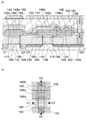
다음에, 도 1a 및 도 1b에 도시하는 반도체 장치의 다른 구성에 대해서 도 6a 및 도 6b를 참조하여 설명한다.Next, another structure of the semiconductor device shown in Figs. 1A and 1B will be described with reference to Figs. 6A and 6B.
<반도체 장치의 단면 구성 및 평면 구성><Sectional and Planar Configuration of Semiconductor Device>
도 6a에는, 반도체 장치의 단면을 도시하고, 도 6b에는 반도체 장치의 평면을 도시한다. 여기서, 도 6a는 도 6b의 C1-C2 및 D1-D2에 있어서의 단면에 상당한다. 도 6a 및 도 6b에 도시하는 반도체 장치는, 도 1a 및 도 1b에서 도시한 반도체 장치와 마찬가지로, 하부에 제 1 반도체 재료를 사용한 트랜지스터(160)를 갖고, 상부에 제 2 반도체 재료를 사용한 트랜지스터(162)를 갖는다. 여기서, 제 1 반도체 재료와 제 2 반도체 재료는 상이한 재료로 하는 것이 바람직하다. 예를 들어, 제 1 반도체 재료를 산화물 반도체 이외의 반도체 재료(실리콘)로 하고, 제 2 반도체 재료를 산화물 반도체로 할 수 있다. 산화물 반도체 이외의 반도체 재료(예를 들어, 단결정 실리콘)를 사용한 트랜지스터는, 고속으로 동작하는 것이 용이하다. 한편, 산화물 반도체를 사용한 트랜지스터는 그 특성 때문에 전하를 장시간 동안 유지할 수 있다.Fig. 6A shows a cross section of the semiconductor device, and Fig. 6B shows a plane of the semiconductor device. Here, Fig. 6A corresponds to a cross section taken along lines C1-C2 and D1-D2 in Fig. 6B. The semiconductor device shown in Figs. 6A and 6B has a
도 6a 및 도 6b에 있어서의 반도체 장치와, 도 1a 및 도 1b에 있어서의 반도체 장치의 차이의 하나는, 트랜지스터(160)와 트랜지스터(162)의 접속 방법이다. 도 1a 및 도 1b에 있어서의 반도체 장치는, 금속 화합물 영역(124)의 일부와 접하는 영역에 전극(126)을 형성하고, 상기 전극(126)을 사이에 두고 하부 트랜지스터(160)의 금속 화합물 영역(124)과, 상부 트랜지스터(162)의 소스 전극 또는 드레인 전극(142b)이 전기적으로 접속된다. 그러나, 도 6a 및 도 6b에 있어서의 반도체 장치는, 상부 트랜지스터(162)의 소스 전극 또는 드레인 전극(142b)을 하부 트랜지스터(160)의 금속 화합물 영역(124)에 직접 접촉시킨다.One of the differences between the semiconductor device of Figs. 6A and 6B and the semiconductor device of Figs. 1A and 1B is the connection method of the
또한, 도 6a 및 도 6b에 있어서의 반도체 장치와, 도 1a 및 도 1b에 있어서의 반도체 장치의 차이의 하나는, 트랜지스터(162)와 상부 배선(156)의 접속 방법이다. 도 1a 및 도 1b에 있어서의 반도체 장치는, 소스 전극 또는 드레인 전극(142b)과 접하는 전극(154)을 형성하고, 상기 전극(154)을 사이에 두고 트랜지스터(162)의 소스 전극 또는 드레인 전극(142b)과 배선(156)이 전기적으로 접속된다. 그러나, 도 6a 및 도 6b에 있어서의 반도체 장치는, 배선(156)을 트랜지스터(162)의 소스 전극 또는 드레인 전극(142b)에 직접 접촉시킨다.One of the differences between the semiconductor device of Figs. 6A and 6B and the semiconductor device of Figs. 1A and 1B is the method of connecting the
또한, 도 6a 및 도 6b에 있어서, 소스 전극 또는 드레인 전극(142b)과, 트랜지스터(160)의 소스 영역 및 드레인 영역의 한쪽이 접하는 영역은, 소스 전극 또는 드레인 전극(142b)과 메모리 셀의 하나와 다른 메모리 셀을 접속하는 배선(156)이 접하는 영역과 중첩된다. 이와 같은 레이아웃을 채용함으로써, 고집적화를 도모할 수 있다.6A and 6B, the region in which the source electrode or the
<반도체 장치의 제작 방법><Manufacturing Method of Semiconductor Device>
도 6a 및 도 6b에 도시하는 반도체 장치의 제작 방법, 특히 상부 트랜지스터(162)의 소스 전극 또는 드레인 전극의 제작 방법에 대해서 설명한다.6A and 6B, a manufacturing method of the source electrode or the drain electrode of the
먼저, 도 2a 내지 도 3d에서 도시한 공정과 마찬가지로, 기판에 채널 형성 영역(116) 및 불순물 영역(120), 금속 화합물 영역(124), 게이트 절연층(108) 및 게이트 전극(110)을 형성한다. 그 후, 형성된 각 구성을 덮도록 절연층(128)을 형성하여 트랜지스터(160)를 형성한다.2A to 3D, a
다음에, 절연층(128)에 CMP 처리를 행하여 게이트 전극(110)의 상면을 노출시킨다. 게이트 전극(110)의 상면을 노출시키는 처리로서는, CMP 처리 이외에 에칭 처리 등을 적용할 수도 있지만, 이후 형성되는 트랜지스터(162)의 특성을 향상시키기 위해서 절연층(128)의 표면은 가능한 한 평탄하게 해 두는 것이 바람직하다.Next, the insulating
다음에, 절연층(128)에 트랜지스터(160)의 금속 화합물 영역(124)까지 도달하는 개구를 형성한다. 상기 개구는 마스크 등을 사용한 선택적인 에칭에 의하여 형성된다.Next, an opening reaching the
그 후, 개구를 포함하는 영역에 PVD법이나 CVD법 등을 사용하여 도전층을 형성한 후, 에칭 처리나 CMP 처리의 방법을 사용하여 상기 도전층의 일부를 선택적으로 제거함으로써 소스 전극 또는 드레인 전극(142a), 소스 전극 또는 드레인 전극(142b)을 형성한다. 개구를 메우도록 도전층을 형성함으로써, 금속 화합물 영역(124)과 소스 전극 또는 드레인 전극(142b)이 직접 접할 수 있다.Thereafter, a conductive layer is formed on the region including the opening using a PVD method, a CVD method, or the like, and then a part of the conductive layer is selectively removed by an etching process or a CMP process, thereby forming a source electrode or a drain electrode
다음에, 도 4b 내지 도 4d에서 도시한 공정과 마찬가지로, 소스 전극 또는 드레인 전극(142a) 및 소스 전극 또는 드레인 전극(142b) 위에 형성된 산화물 반도체층(144)과, 산화물 반도체층(144)에 접하는 게이트 절연층(146)과, 게이트 절연층(146) 위에 형성된 게이트 전극(148a)과, 게이트 전극(148a) 위에 형성된 절연층(150)과, 절연층(150) 위에 형성된 전극(149a)을 각각 형성한다.4B to 4D, an
그 후, 도 5a 내지 도 5c에서 도시한 공정과 마찬가지로, 전극(149a)을 덮도록 절연층(151), 절연층(152)을 형성한다. 절연층(151) 및 절연층(152)을 형성한 후, 상기 절연층(152), 절연층(151), 절연층(150), 게이트 절연층(146)에 소스 전극 또는 드레인 전극(142b)까지 도달하는 개구를 형성한다. 상기 개구는 마스크 등을 사용한 선택적인 에칭에 의하여 형성된다.Thereafter, an insulating
그 후, 개구를 포함하는 영역에 PVD법이나 CVD법 등을 사용하여 도전층을 형성한 후, 에칭 처리나 CMP 처리 등의 방법을 사용하여 상기 도전층의 일부를 선택적으로 제거함으로써 배선(156)을 형성한다.Thereafter, a conductive layer is formed on the region including the opening using a PVD method, a CVD method, or the like, and then a part of the conductive layer is selectively removed by a method such as an etching process or a CMP process, .
상술한 공정에 의하여 도 6a 및 도 6b에 도시하는 반도체 장치를 형성할 수 있다. 도 6a 및 도 6b에 도시하는 반도체 장치는, 하부 트랜지스터(160)와 상부 트랜지스터(162)의 접속, 및 상부 트랜지스터(162)와 배선(156)의 접속을 각각 전극을 형성하지 않고 상부 트랜지스터(162)의 소스 전극 또는 드레인 전극(142b)을 사용하여 직접적으로 행한다. 따라서, 전극의 형성 공정을 생략할 수 있다. 이로써, 본 실시형태에서 나타내는 반도체 장치는 저비용으로 제작할 수 있다.The semiconductor device shown in Figs. 6A and 6B can be formed by the above-described processes. The semiconductor device shown in Figs. 6A and 6B is a semiconductor device in which the connection of the
이상, 본 실시형태에 나타내는 구성, 방법 등은, 다른 실시형태에 나타내는 구성, 방법 등과 적절히 조합하여 사용할 수 있다.The configurations, methods, and the like described in this embodiment can be appropriately combined with the configurations, methods, and the like described in the other embodiments.
(실시형태 2)(Embodiment 2)
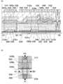
본 실시형태에서는, 개시하는 발명의 별도의 일 형태에 따른 반도체 장치의 구성 및 그 제작 방법에 대해서 도 7a 내지 도 10b를 참조하여 설명한다.In the present embodiment, a structure of a semiconductor device and a manufacturing method thereof according to another embodiment of the disclosed invention will be described with reference to Figs. 7A to 10B.
<반도체 장치의 단면 구성 및 평면 구성><Sectional and Planar Configuration of Semiconductor Device>
도 7a 및 도 7b는, 본 실시형태에 따른 반도체 장치의 구성의 일례이다. 도 7a에는, 반도체 장치의 단면을 도시하고, 도 7b에는 반도체 장치의 평면을 도시한다. 여기서, 도 7a는 도 7b의 E1-E2 및 F1-F2에 있어서의 단면에 상당한다. 도 7a 및 도 7b에 도시하는 반도체 장치는, 하부에 제 1 반도체 재료를 사용한 트랜지스터(560)를 갖고, 상부에 제 2 반도체 재료를 사용한 트랜지스터(562)를 갖는다. 여기서, 제 1 반도체 재료와 제 2 반도체 재료는 상이한 재료로 하는 것이 바람직하다. 예를 들어, 제 1 반도체 재료를 산화물 반도체 이외의 재료(실리콘) 등으로 하고, 제 2 반도체 재료를 산화물 반도체로 할 수 있다. 산화물 반도체 이외의 반도체 재료(예를 들어, 단결정 실리콘)를 사용한 트랜지스터는 고속 동작이 용이하다. 한편, 산화물 반도체를 사용한 트랜지스터는, 그 특성 특성에 의하여 전하를 장시간 동안 유지할 수 있다.7A and 7B are an example of the configuration of the semiconductor device according to the present embodiment. Fig. 7A shows a cross section of the semiconductor device, and Fig. 7B shows a plane of the semiconductor device. Here, FIG. 7A corresponds to a cross section taken along lines E1-E2 and F1-F2 in FIG. 7B. The semiconductor device shown in Figs. 7A and 7B has a
또한, 상기 트랜지스터 중 양쪽 모두는 n채널형 트랜지스터로서 설명하지만, p채널형 트랜지스터를 사용할 수 있는 것은 물론이다. 또한, 개시하는 발명의 기술적인 본질은, 정보를 유지하기 위해서 산화물 반도체와 같은 오프 전류를 충분히 저감시킬 수 있는 재료를 트랜지스터(562)에 사용하는 점에 있기 때문에, 반도체 장치에 사용되는 재료나 반도체 장치의 구조 등, 반도체 장치의 구체적인 구성은 여기서 나타내는 구성에 한정될 필요는 없다.Although both of the transistors are described as n-channel transistors, it goes without saying that p-channel transistors can be used. The technical nature of the disclosed invention is that the
도 7a 및 도 7b에 도시하는 트랜지스터(560)는, 베이스 기판(500) 위의 반도체층 중에 형성된 채널 형성 영역(526)과, 채널 형성 영역(526)을 끼우도록 형성된 불순물 영역(528)과, 채널 형성 영역(526) 위에 형성된 게이트 절연층(522a)과, 게이트 절연층(522a) 위에 형성된 게이트 전극(524a)을 갖는다. 즉, 도 7a 및 도 7b에 있어서의 트랜지스터(560)와, 도 1a 및 도 1b에 있어서의 트랜지스터(160)와의 차이 중의 하나는, 트랜지스터의 채널 형성 영역이 반도체층 중에 형성되는지 여부에 있다. 도 1a 및 도 1b에서는, 반도체 기판을 사용하지만, 도 7a 및 도 7b에서는 SOI 기판을 사용하기 때문에, 그 점이 차이점이라고 말할 수도 있다. 또한, 모든 도면에 있어서, 명시적(明示的)으로는 소스 전극이나 드레인 전극을 갖지 않는 경우가 있지만, 편의상, 이와 같은 상태를 포함하여 트랜지스터라고 부르는 경우가 있다.7A and 7B includes a
트랜지스터(560)의 금속 화합물 영역(124)의 일부에는, 전극(530)이 접속된다. 여기서, 전극(530)은 트랜지스터(560)의 소스 전극이나 드레인 전극으로서 기능한다. 또한, 트랜지스터(560)를 덮도록 절연층(534)이 형성된다. 또한, 고집적화를 실현하기 위해서는, 도 7a 및 도 7b에 도시하는 바와 같이, 트랜지스터(560)가 사이드 월 절연층을 갖지 않는 구성으로 하는 것이 바람직하다. 한편, 트랜지스터(560)의 특성을 중요시하는 경우에는, 게이트 전극(524a)의 측면에 사이드 월 절연층을 형성하고, 불순물 농도가 상이한 영역을 포함하는 불순물 영역(528)을 형성하여도 좋다.An
도 7a 및 도 7b에 있어서의 트랜지스터(562)는, 도 1a 및 도 1b에 있어서의 트랜지스터(162)와 마찬가지다. 즉, 도 7a 및 도 7b에 있어서의 트랜지스터(562)는 절연층(534) 위에 형성된 소스 전극 또는 드레인 전극(542a), 및 소스 전극 또는 드레인 전극(542b)과, 소스 전극 또는 드레인 전극(542a), 및 소스 전극 또는 드레인 전극(542b)과 전기적으로 접속되는 산화물 반도체층(544)과, 소스 전극 또는 드레인 전극(542a), 소스 전극 또는 드레인 전극(542b), 산화물 반도체층(544)을 덮는 게이트 절연층(546)과, 게이트 절연층(546) 위에 산화물 반도체층(544)과 중첩하도록 형성된 게이트 전극(548a)을 갖는다.The
또한, 도 7a 및 도 7b에 있어서의 용량 소자(564)는, 도 1a 및 도 1b에 있어서의 용량 소자(164)와 마찬가지다. 즉, 도 7a 및 도 7b에 있어서의 용량 소자(564)는, 소스 전극 또는 드레인 전극(542a), 산화물 반도체층(544), 게이트 절연층(546), 절연층(550), 및 전극(549a)으로 구성된다. 즉, 소스 전극 또는 드레인 전극(542a)은 용량 소자(564)의 한쪽의 전극으로서 기능하고, 전극(549a)은 용량 소자(564)의 다른 쪽의 전극으로서 기능한다. 그 이외의 자세한 내용에 대해서는, 상술한 실시형태를 참작할 수 있다.The
트랜지스터(562) 및 용량 소자(564) 위에 절연층(551)이 형성되고, 절연층(551) 위에는 절연층(552)이 형성되고, 게이트 절연층(546), 절연층(550), 절연층(551), 절연층(552) 등에 형성된 개구에 전극(554)이 형성되고, 절연층(552) 위에는 전극(554)과 접속하는 배선(556)이 형성되는 점에 대해서도 도 1a 및 도 1b와 마찬가지다.An insulating
<SOI 기판의 제작 방법><Manufacturing Method of SOI Substrate>
다음에, 상기 반도체 장치의 제작에 사용되는 SOI 기판의 제작 방법의 일례에 대해서 도 8a 내지 도 8h를 참조하여 설명한다.Next, an example of a method of manufacturing an SOI substrate used for manufacturing the semiconductor device will be described with reference to Figs. 8A to 8H.
우선, 베이스 기판(500)을 준비한다(도 8a 참조). 베이스 기판(500)으로서는, 절연체로 이루어지는 기판을 사용할 수 있다. 구체적으로는, 알루미노 실리케이트 유리, 알루미노 보로실리케이트 유리, 바륨 보로실리케이트 유리와 같은 전자 공업용으로 사용되는 각종 유리 기판, 석영 기판, 세라믹 기판, 사파이어 기판을 들 수 있다. 또한, 질화실리콘과 산화알루미늄을 주성분으로 한 열 팽창 계수가 실리콘에 가까운 세라믹 기판을 사용하여도 좋다.First, a
또한, 베이스 기판(500)으로서 단결정 실리콘 기판, 단결정 게르마늄 기판 등의 반도체 기판을 사용하여도 좋다. 베이스 기판(500)으로서 반도체 기판을 사용하는 경우에는, 유리 기판 등을 사용하는 경우와 비교하여, 열 처리의 온도 조건이 완화되기 때문에, 질이 양호한 SOI 기판을 얻는 것이 용이해진다. 여기서, 반도체 기판으로서는, 태양 전지급(太陽電池級) 실리콘(SOG-Si: Solar Grade Silicon) 기판 등을 사용하여도 좋다. 또한, 다결정 반도체 기판을 사용하여도 좋다. 태양 전지급 실리콘이나 다결정 반도체 기판 등을 사용하는 경우에는, 단결정 실리콘 기판 등을 사용하는 경우와 비교하여 제작 비용을 억제할 수 있다.As the
본 실시형태에서는, 베이스 기판(500)으로서 유리 기판을 사용하는 경우에 대해서 설명한다. 베이스 기판(500)으로서 대면적화가 가능하고 저렴한 유리 기판을 사용함으로써, 저비용화를 도모할 수 있다.In this embodiment, a case of using a glass substrate as the
상기 베이스 기판(500)에 대해서는, 그 표면을 미리 세정해 두는 것이 바람직하다. 구체적으로는, 베이스 기판(500)에 대해서 염산과산화수소수 혼합 용액(HPM), 황산과산화수소수 혼합 용액(SPM), 암모니아과산화수소수 혼합 용액(APM), 희불산(DHF), FPM(불산, 과산화수소수, 순수의 혼합액) 등을 사용하여 초음파 세정을 행한다. 이와 같은 세정 처리를 행함으로써, 베이스 기판(500) 표면의 평탄성 향상이나, 베이스 기판(500) 표면에 잔존하는 연마 입자의 제거 등이 실현된다.The surface of the
다음에, 베이스 기판(500) 표면에는 질소 함유층(502: 예를 들어, 질화실리콘막(SiNx)이나 질화산화실리콘막(SiNxOy)(x>y) 등의 질소를 함유하는 절연막을 포함하는 층)을 형성한다(도 8b 참조). 질소 함유층(502)은, CVD법, 스퍼터링법 등을 사용하여 형성할 수 있다.Next, on the surface of the
본 실시형태에 있어서 형성되는 질소 함유층(502)은, 이후에 단결정 반도체층을 접합하기 위한 층(접합층)이 된다. 또한, 질소 함유층(502)은, 베이스 기판에 함유되는 나트륨(Na) 등의 불순물이 단결정 반도체층으로 확산되는 것을 방지하기 위한 베리어층으로서도 기능한다.The nitrogen-containing
상술한 바와 같이, 본 실시형태에서는 질소 함유층(502)을 접합층으로서 사용하기 때문에, 그 표면이 소정의 평탄성을 갖도록 질소 함유층(502)을 형성하는 것이 바람직하다. 구체적으로는, 표면의 평균면 거칠기(Ra; 산술 평균 거칠기라고도 한다)가 0.50nm 이하, 제곱 평균 거칠기(RMS)가 0.60nm 이하, 보다 바람직하게는, 평균면 거칠기가 0.35nm 이하, 제곱 평균 거칠기가 0.45nm 이하가 되도록 질소 함유층(502)을 형성한다. 또한, 상술한 평균면 거칠기나 제곱 평균 거칠기에는, 예를 들어 10μm×10μm의 영역에 있어서 측정된 값을 사용할 수 있다. 막 두께는, 10nm 이상 200nm 이하, 바람직하게는 50nm 이상 100nm 이하의 범위로 한다. 이와 같이, 표면의 평탄성을 높임으로써, 이후의 공정에 있어서 단결정 반도체층의 접합 불량을 방지할 수 있다.As described above, in the present embodiment, since the nitrogen-containing
다음에, 본드 기판을 준비한다. 여기서는, 본드 기판으로서 단결정 반도체 기판(510)을 사용한다(도 8c 참조). 또한, 여기서는 본드 기판으로서 단결정의 기판을 사용하지만, 본드 기판의 결정성을 단결정에 한정할 필요는 없다.Next, a bond substrate is prepared. Here, the single
단결정 반도체 기판(510)으로서는, 예를 들어, 단결정 실리콘 기판, 단결정 게르마늄 기판, 단결정 실리콘 게르마늄 기판 등, 제 14족 원소로 이루어진 단결정 반도체 기판을 사용할 수 있다. 또한, 갈륨비소나 인듐인 등의 화합물 반도체 기판을 사용할 수도 있다. 시판되고 있는 실리콘 기판으로서는, 직경 5인치(125mm), 직경 6인치(150mm), 직경 8인치(200mm), 직경 12인치(300mm), 직경 16인치(400mm) 사이즈의 원형의 실리콘 기판이 대표적이다. 또한, 단결정 반도체 기판(510)의 형상은 원형에 한정되지 않고, 예를 들어, 직사각형 등으로 가공한 것이라도 좋다. 또한, 단결정 반도체 기판(510)은, CZ(초크랄스키)법이나 FZ(플로팅 존)법을 사용하여 제작할 수 있다.As the single
단결정 반도체 기판(510)의 표면에는 산화막(512)을 형성한다(도 8d 참조). 또한, 오염물 제거의 관점에서, 산화막(512)을 형성하기 전에 염산과산화수소수 혼합 용액(HPM), 황산과산화수소수 혼합 용액(SPM), 암모니아과산화수소수 혼합 용액(APM), 희불산(DHF), FPM(불산, 과산화수소수, 순수의 혼합액) 등을 사용하여 단결정 반도체 기판(510)의 표면을 세정해 두는 것에 바람직하다. 희불산과 오존수를 교체로 토출시켜 세정하여도 좋다.An
산화막(512)은, 예를 들어, 산화실리콘막, 산화질화실리콘막 등을 단층으로 형성, 또는 적층시켜 형성할 수 있다. 상기 산화막(512)의 제작 방법으로서는, 열 산화법, CVD법, 스퍼터링법 등이 있다. 또한, CVD법을 사용하여 산화막(512)을 형성하는 경우에, 양호한 접합을 실현하기 위해서는, 테트라에톡시실란(약칭: TEOS: 화학식 Si(OC2H5)4) 등의 유기 실란을 사용하여 산화실리콘막을 형성하는 것이 바람직하다.The
본 실시형태에서는, 단결정 반도체 기판(510)에 열 산화 처리를 행함으로써 산화막(512)(여기서는, SiOx막)을 형성한다. 열 산화 처리는, 산화성 분위기 중에 할로겐을 첨가하여 행하는 것이 바람직하다.In the present embodiment, the single
예를 들어, 염소(Cl)가 첨가된 산화성 분위기 중에서 단결정 반도체 기판(510)에 열 산화 처리를 행함으로써, 염소 산화된 산화막(512)을 형성할 수 있다. 이 경우, 산화막(512)은 염소 원자를 함유한 막이 된다. 이와 같은 염소 산화에 의하여 외인성(外因性)의 불순물인 중금속(예를 들어, 철(Fe), 크롬(Cr), 니켈(Ni), 몰리브덴(Mo) 등)을 포집(捕集)하여 금속의 염화물을 형성하고, 이것을 밖으로 제거하여 단결정 반도체 기판(510)의 오염을 저감시킬 수 있다. 또한, 베이스 기판(500)과 접합한 후에, 베이스 기판에서의 Na 등의 불순물을 고정하여, 단결정 반도체 기판(510)이 오염되는 것을 방지할 수 있다.For example, a chlorine-oxidized
또한, 산화막(512)에 함유시키는 할로겐 원자는 염소 원자에 한정되지 않는다. 산화막(512)에는 불소 원자를 함유시켜도 좋다. 단결정 반도체 기판(510) 표면을 불소 산화하는 방법으로서는, 불산(HF) 용액에 침지시킨 후에 산화성 분위기 중에서 열 산화 처리를 행하는 방법이나, 삼불화질소(NF3)을 산화성 분위기에 첨가하여 열 산화 처리를 행하는 방법 등이 있다.Further, the halogen atom contained in the
다음에, 전계에 의하여 가속된 이온을 단결정 반도체 기판(510)에 조사하여 첨가함으로써, 단결정 반도체 기판(510)의 소정 깊이에 결정 구조가 손상된 취화 영역(514)을 형성한다(도 8e 참조).Next, ions accelerated by an electric field are irradiated and added to the single
취화 영역(514)이 형성되는 영역의 깊이는, 이온의 운동 에너지, 이온의 질량과 전하, 이온의 입사각 등에 의하여 조절할 수 있다. 또한, 취화 영역(514)은, 이온의 평균 침입 깊이와 거의 같은 깊이의 영역에 형성된다. 그래서, 이온을 첨가하는 깊이로, 단결정 반도체 기판(510)으로부터 분리되는 단결정 반도체층의 두께를 조절할 수 있다. 예를 들어, 단결정 반도체층의 두께가, 10nm 이상 500nm 이하, 바람직하게는 50nm 이상 200nm 이하 정도가 되도록 평균 침입 깊이를 조절하면 좋다.The depth of the region where the
상기 이온의 조사 처리는, 이온 도핑 장치나 이온 주입 장치를 사용하여 행할 수 있다. 이온 도핑 장치의 대표적인 예로서는, 프로세스 가스를 플라즈마 여기하여 생성된 모든 이온종을 피처리체에 조사하는 비질량 분리형의 장치가 있다. 상기 장치에서는, 플라즈마 중의 이온종을 질량분리하지 않고 피처리체에 조사한다. 이것에 대해서, 이온 주입 장치는, 질량 분리형의 장치이다. 이온 주입 장치에서는, 플라즈마 중의 이온종을 질량 분리하고, 어느 특정의 질량의 이온종을 피처리체에 조사한다.The ion irradiation treatment can be performed using an ion doping apparatus or an ion implantation apparatus. As a representative example of the ion doping apparatus, there is a non-mass separation type apparatus for irradiating the object to be processed with all the ion species generated by plasma excitation of the process gas. In this apparatus, ion species in a plasma are irradiated to a workpiece without mass separation. On the other hand, the ion implantation apparatus is a mass separation type apparatus. In the ion implantation apparatus, ion species in a plasma are mass-separated, and an ion species of a specific mass is irradiated to an object to be processed.
본 실시형태에서는, 이온 도핑 장치를 사용하여, 수소를 단결정 반도체 기판(510)에 첨가하는 예에 대해서 설명한다. 소스 가스로서는, 수소를 포함하는 가스를 사용한다. 조사하는 이온에 대해서는, H3+의 비율을 높이면 좋다. 구체적으로는, H+, H2+, H3+의 총량에 대해서 H3+의 비율이 50% 이상(보다 바람직하게는 80% 이상)이 되도록 한다. H3+의 비율을 높임으로써, 이온 조사의 효율을 향상시킬 수 있다.In this embodiment, an example of adding hydrogen to the single
또한, 첨가하는 이온은 수소에 한정되지 않는다. 헬륨 등의 이온을 첨가하여도 좋다. 또한, 첨가하는 이온은 1종류에 한정되지 않고, 복수 종류의 이온을 첨가하여도 좋다. 예를 들어, 이온 도핑 장치를 사용하여 수소와 헬륨을 동시에 조사하는 경우는, 수소와 헬륨을 각각 다른 공정에 의하여 조사하는 경우와 비교하여 공정수를 저감할 수 있는 것과 함께, 이후의 단결정 반도체층의 표면 거칠기를 억제할 수 있다.Further, the ion to be added is not limited to hydrogen. Ions such as helium may be added. The number of ions to be added is not limited to one, and a plurality of kinds of ions may be added. For example, when hydrogen and helium are simultaneously irradiated using an ion doping apparatus, the number of processes can be reduced as compared with the case where hydrogen and helium are separately irradiated by different processes, Can be suppressed.
또한, 이온 도핑 장치를 사용하여 취화 영역(514)을 형성하는 경우에는, 중금속도 동시에 첨가될 우려가 있지만, 할로겐 원소를 함유하는 산화막(512)을 사이에 두고, 이온의 조사를 행함으로써 이들 중금속에 의한 단결정 반도체 기판(510)의 오염을 방지할 수 있다.Further, when the
다음에, 베이스 기판(500)과 단결정 반도체 기판(510)을 대향시켜, 질소 함유층(502) 표면과 산화막(512)을 밀착시킨다. 이로써, 베이스 기판(500)과 단결정 반도체 기판(510)이 접합된다(도 8f 참조).Next, the
접합할 때는, 베이스 기판(500) 또는 단결정 반도체 기판(510)의 1개소에 0.001N/cm2 이상 100N/cm2 이하, 예를 들어, 1N/cm2 이상 20N/cm2 이하의 압력을 가하는 것이 바람직하다. 압력을 가하여 접합면을 접근시켜 밀착시키면, 밀착시킨 부분에서 질소 함유층(502)과 산화막(512)이 접합되고, 상기 부분을 시점(始點)으로 하여 자발적인 접합이 대략 전체면에 미친다. 이 접합에는, 반 데르 발스 힘(van der Waals' force)이나 수소 결합이 작용되고, 상온으로 행할 수 있다.When joined, the
또한, 단결정 반도체 기판(510)과 베이스 기판(500)을 접합하기 전에, 접합에 따른 표면에 대해서 표면 처리를 행하는 것이 바람직하다. 표면 처리를 행함으로써, 단결정 반도체 기판(510)과 베이스 기판(500)의 접합 계면에서의 접합 강도를 향상시킬 수 있다.Before bonding the single
표면 처리로서는, 웨트 처리, 드라이 처리, 또는 웨트 처리 및 드라이 처리의 조합을 사용할 수 있다. 또한, 다른 웨트 처리끼리를 조합하여 사용하여도 좋고, 다른 드라이 처리끼리를 조합하여 사용하여도 좋다.As the surface treatment, a wet treatment, a dry treatment, or a combination of a wet treatment and a dry treatment may be used. In addition, other wet treatments may be used in combination, or different dry treatments may be used in combination.
또한, 접합한 후에는, 접합 강도를 증가시키기 위한 열 처리를 행하여도 좋다. 이 열 처리의 온도는, 취화 영역(514)에 있어서의 분리가 생기지 않는 온도(예를 들어, 실온 이상 400℃ 미만)로 한다. 또한, 이 온도 범위에서 가열하면서, 질소 함유층(502)과 산화막(512)을 접합시켜도 좋다. 상기 열 처리에서는, 확산로, 저항 가열로 등의 가열로, RTA(순간 열어닐, Rapid Thermal Anneal) 장치, 마이크로파 가열 장치 등을 사용할 수 있다. 또한, 상기 온도 조건은 단순히 일례에 불과하고, 개시하는 발명의 일 형태가 이것에 한정하여 해석되는 것은 아니다.After the bonding, heat treatment for increasing the bonding strength may be performed. The temperature of this heat treatment is set to a temperature at which separation in the embrittled
다음에, 열 처리를 행하여 단결정 반도체 기판(510)을 취화 영역에서 분리함으로써, 베이스 기판(500) 위에, 질소 함유층(502) 및 산화막(512)을 사이에 두고 단결정 반도체층(516)을 형성한다(도 8g 참조).Next, a single
상기 분리를 행할 때의 열 처리 온도는 가능한 한 낮은 온도가 바람직하다. 그 이유는, 분리를 행할 때의 온도가 낮을수록, 단결정 반도체층(516)의 표면 거칠기를 억제할 수 있기 때문이다. 구체적으로는, 예를 들어, 상기 분리를 행할 때의 열 처리 온도는 300℃ 이상 600℃ 이하로 하면 좋고, 400℃ 이상 500℃ 이하로 하면 보다 효과적이다.The heat treatment temperature at the time of performing the separation is preferably as low as possible. This is because the surface roughness of the single
또한, 단결정 반도체 기판(510)을 분리한 후에는, 단결정 반도체층(516)에 대해서 500℃ 이상의 온도에서 열 처리를 행하여, 단결정 반도체층(516) 중에 잔존하는 수소의 농도를 저감시켜도 좋다.After the single
다음에, 단결정 반도체층(516)의 표면에 레이저 광을 조사함으로써, 표면의 평탄성을 향상시키고, 또 결함을 저감시킨 단결정 반도체층(518)을 형성한다(도 8h 참조). 또한, 레이저 광의 조사 처리 대신에 열 처리를 행하여도 좋다.Next, the surface of the single
또한, 본 실시형태에서는, 단결정 반도체층(516)의 분리에 따른 열 처리 직후에, 레이저 광의 조사 처리를 행하지만, 본 발명의 일 형태는 이것에 한정하여 해석되지 않는다. 단결정 반도체층(516)의 분리에 따른 열 처리 후에 에칭 처리를 행하여, 단결정 반도체층(516) 표면의 결함이 많은 영역을 제거한 후에 레이저 광의 조사 처리를 행하여도 좋고, 단결정 반도체층(516) 표면의 평탄성을 향상시킨 후에 레이저 광의 조사를 행하여도 좋다. 또한, 상기 에칭 처리로서는, 웨트 에칭 또는 드라이 에칭의 어느 쪽을 사용하여도 좋다. 또한, 본 실시형태에 있어서는 상술한 바와 같이, 레이저 광을 조사한 후에, 단결정 반도체층(516)의 막 두께를 작게 하는 박막화 공정을 행하여도 좋다. 단결정 반도체층(516)의 박막화에는, 드라이 에칭 또는 웨트 에칭의 한쪽, 또는 양쪽을 조합하여 사용하면 좋다.In the present embodiment, the irradiation treatment of the laser beam is performed immediately after the heat treatment according to the separation of the single
상술한 공정에 의하여, 특성이 양호한 단결정 반도체층(518)을 갖는 SOI 기판을 얻을 수 있다(도 8h 참조).By the above-described process, an SOI substrate having a single
<반도체 장치의 제작 방법><Manufacturing Method of Semiconductor Device>
다음에, 상술한 SOI 기판을 사용한 반도체 장치의 제작 방법, 특히 트랜지스터(560)의 제작 방법에 대해서 도 9a 내지 도 9e를 참조하여 설명한다. 또한, 도 9a 내지 도 9e는, 도 8a 내지 도 8h에 도시하는 방법에 의하여 제작한 SOI 기판의 일부이고, 도 7a의 일부에 상당하는 단면도이다.Next, a method of manufacturing a semiconductor device using the above-described SOI substrate, in particular, a method of manufacturing the
우선, 단결정 반도체층(518)을 섬 형상으로 가공하여 반도체층(520)을 형성한다(도 9a 참조). 또한, 이 공정의 전후에서 트랜지스터의 임계값 전압을 제어하기 위해서 n형의 도전성을 부여하는 불순물 원소나, p형의 도전성을 부여하는 불순물 원소를 반도체층에 첨가하여도 좋다. 반도체가 실리콘인 경우, n형의 도전성을 부여하는 불순물 원소로서는, 예를 들어 인이나 비소 등을 사용할 수 있다. 또한, p형의 도전성을 부여하는 불순물 원소로서는, 예를 들어 붕소, 알루미늄, 갈륨 등을 사용할 수 있다.First, the single
다음에, 반도체층(520)을 덮도록 절연층(522)을 형성하고, 절연층(522) 위의 반도체층(520)과 중첩하는 영역에 도전층(524)을 형성한다(도 9b 참조).Next, an insulating
절연층(522)은, 이후 게이트 절연층이 된다. 절연층(522)은, 예를 들어 반도체층(520) 표면의 열 처리(열 산화 처리나 열 질화 처리 등)에 의하여 형성할 수 있다. 열 처리 대신에 고밀도 플라즈마 처리를 적용하여도 좋다. 고밀도 플라즈마 처리는 예를 들어, He, Ar, Kr, Xe 등의 희 가스, 산소, 산화질소, 암모니아, 질소, 수소 등 중 어느 가스의 혼합 가스를 사용하여 행할 수 있다. 물론, CVD법이나 스퍼터링법 등을 사용하여 절연층을 형성하여도 좋다. 상기 절연층은 산화실리콘, 산화질화실리콘, 질화실리콘, 산화하프늄, 산화알루미늄, 산화탄탈, 산화이트륨, 하프늄실리케이트(HfSixOy(x>0, y>0)), 질소가 첨가된 하프늄실리케이트(HfSixOyNz(x>0, y>0, z>0)), 질소가 첨가된 하프늄알루미네이트(HfAlxOyNz(x>0, y>0, z>0)) 등을 포함하는 단층 구조 또는 적층 구조로 하는 것이 바람직하다. 또한, 절연층의 두께는 예를 들어, 1nm 이상 100nm 이하, 바람직하게는 10nm 이상 50nm 이하로 할 수 있다. 여기서는, 플라즈마 CVD법을 사용하여 산화실리콘을 포함하는 절연층을 단층으로 형성한다.The insulating
도전층(524)은 이후 게이트 전극이 된다. 도전층(524)은, 알루미늄이나 구리, 티타늄, 탄탈, 텅스텐 등의 금속 재료를 사용하여 형성할 수 있다. 또한, 다결정 실리콘 등의 반도체 재료를 사용하여 도전 재료를 포함하는 층을 형성하여도 좋다. 형성 방법에 대해서도 특히 한정되지 않고, 증착법, CVD법, 스퍼터링법, 스핀코팅법 등의 각종 성막 방법을 사용할 수 있다. 또한, 본 실시형태에서는, 도전 재료를 포함하는 층을 금속 재료를 사용하여 형성하는 경우의 일례에 대해서 나타낸다.The
다음에, 절연층(522) 및 도전층(524)을 선택적으로 에칭하여 반도체층(520)의 상방에 게이트 절연층(522a) 및 게이트 전극(524a)을 형성한다(도 9c 참조). 상기 에칭에는, 드라이 에칭을 사용하는 것이 바람직하지만, 웨트 에칭을 사용하여도 좋다. 에칭 가스나 에칭 액에 대해서는 피(被)에칭 재료에 따라 적절히 선택할 수 있다.Next, the insulating
다음에, 게이트 전극(524a)을 마스크로 하여 일 도전형을 부여하는 불순물 원소를 반도체층(520)에 첨가하여 채널 형성 영역(526) 및 불순물 영역(528)을 형성한다(도 9d 참조). 또한, 여기서는 n형 트랜지스터를 형성하기 위해서, 인(P)이나 비소(As)를 첨가하지만, p형 트랜지스터를 형성하는 경우에는, 붕소(B)나 알루미늄(Al), 갈륨(Ga) 등의 불순물 원소를 첨가하면 좋다. 여기서, 첨가되는 불순물의 농도는 적절히 설정할 수 있다. 또한, 불순물 원소를 첨가한 후에는, 활성화시키기 위한 열 처리를 행한다.Next, an impurity element imparting one conductivity type is added to the
또한, 반도체층(520)이 실리콘을 포함하는 재료로 이루어지는 경우에는, 소스 영역 및 드레인 영역을 더 저저항화시키기 위해서, 반도체층(520)의 일부를 실리사이드화한 실리사이드 영역을 형성하여도 좋다. 실리사이드 영역의 형성은, 반도체층에 금속을 접촉시켜, 가열 처리(예를 들어, GRTA법, LRTA법, 레이저 광의 조사 등)에 의하여 반도체층 중의 실리콘과 금속을 반응시켜 행한다. 실리사이드로서는, 예를 들어, 코발트 실리사이드나 니켈 실리사이드를 형성하면 좋다. 반도체층(520)이 얇은 경우에는, 반도체층(520)의 저면(底面) 부분까지 실리사이드 반응을 진행시켜도 좋다. 실리사이드화에 사용할 수 있는 금속 재료로서는, 코발트나 니켈 이외에, 티타늄, 텅스텐, 몰리브덴, 지르코늄, 하프늄, 탄탈, 바나듐, 네오디뮴, 크롬, 백금, 팔라듐 등을 들 수 있다.In the case where the
다음에, 불순물 영역(528)의 일부와 접하는 영역에, 전극(530)을 형성하고, 그 후 형성된 각 구성을 덮도록 절연층(534)을 형성한다(도 9e 참조).Next, an
전극(530)은 예를 들어 도전 재료를 포함하는 층을 형성한 후에, 상기 층을 선택적으로 에칭함으로써 형성된다. 도전 재료를 포함하는 층은, 알루미늄이나 구리, 티타늄, 탄탈, 텅스텐 등의 금속 재료를 사용하여 형성할 수 있다. 또한, 다결정 실리콘 등의 반도체 재료를 사용하여 도전 재료를 포함하는 층을 형성하여도 좋다. 형성 방법도 특히 한정되지 않고, 증착법, CVD법, 스퍼터링법, 스핀코팅법 등의 각종 성막 방법을 사용할 수 있다.
또한, 절연층(534)을 형성한 후에, 절연층(534)에 불순물 영역(528)까지 도달하는 개구를 형성하고, 상기 개구를 메우도록 전극(530)을 형성할 수도 있다.It is also possible to form an opening reaching the
절연층(534)은, 산화실리콘, 산화질화실리콘, 질화실리콘, 산화알루미늄 등의 무기 절연 재료를 포함하는 재료를 사용하여 형성할 수 있다. 특히, 절연층(534)에 유전율이 낮은(low-k) 재료를 사용함으로써, 각종 전극이나 배선의 중첩에 기인하는 용량을 충분히 저감시킬 수 있기 때문에 바람직하다. 또한, 절연층(534)에는, 이들의 재료를 사용한 다공성의 절연층을 적용하여도 좋다. 다공성의 절연층에서는, 밀도가 높은 절연층과 비교하여 유전율이 저하하기 때문에, 전극이나 배선에 기인하는 용량을 더 저감시킬 수 있다. 또한, 절연층(534)은 폴리이미드, 아크릴 등의 유기 절연 재료를 사용하여 형성할 수도 있다. 또한, 여기서는, 절연층(534)의 적층 구조로 하지만, 개시하는 발명의 일 형태는 이것에 한정되지 않는다. 1층으로 구성하여도 좋고, 3층 이상의 적층 구조로 구성하여도 좋다.The insulating
이상에 의해 SOI 기판을 사용한 트랜지스터(560)가 형성된다(도 9e 참조). 산화물 반도체 이외의 재료를 사용한 트랜지스터(560)는, 고속 동작이 가능하기 때문에, 상기 트랜지스터를 판독 트랜지스터로서 사용함으로써, 판독 동작을 고속화할 수 있다. 또한, 트랜지스터(560)를 사용하여 다른 논리 회로(연산 회로라고도 한다) 등을 구성할 수도 있다.Thus, the
그 후, 절연층(534)에 CMP 처리를 행하여 게이트 전극(524a) 및 전극(530)의 상면을 노출시킨다(도시하지 않는다). 게이트 전극(524a) 및 전극(530)의 상면을 노출시키는 처리로서는, CMP 처리 이외에 에칭 처리 등을 적용할 수도 있지만, 이후 형성되는 트랜지스터(562)의 특성을 향상시키기 위해서 절연층(534)의 표면은 가능한 한 평탄하게 해 두는 것이 바람직하다.Thereafter, a CMP process is performed on the insulating
또한, 상술한 각 공정의 전후에는, 전극이나 배선, 반도체층, 절연층 등을 형성하는 공정을 더 포함하여도 좋다. 예를 들어, 배선의 구조로서, 절연층 및 도전층의 적층 구조로 이루어지는 다층 배선 구조를 채용하여 고도로 집적화된 반도체 장치를 실현할 수도 있다.Further, before or after each of the above-described steps, a step of forming an electrode, a wiring, a semiconductor layer, an insulating layer, and the like may be further included. For example, as a wiring structure, a highly integrated semiconductor device can be realized by employing a multilayer wiring structure having a laminated structure of an insulating layer and a conductive layer.
그 후, 트랜지스터(560)와 전기적으로 접속하는 트랜지스터(562) 및 용량 소자(564)를 형성한다(도 7a 참조). 트랜지스터(562) 및 용량 소자(564)의 제작 방법은, 트랜지스터(162) 및 용량 소자(164)의 경우와 마찬가지기 때문에, 여기서는 생략한다. 제작 방법의 자세한 내용에 대해서는, 상술한 실시형태를 참작할 수 있다.Thereafter, a
<변형예><Modifications>
다음에, 도 7a 및 도 7b에 도시하는 반도체 장치의 다른 구성에 대해서 도 10a 및 도 10b를 참조하여 설명한다.Next, another structure of the semiconductor device shown in Figs. 7A and 7B will be described with reference to Figs. 10A and 10B.
<반도체 장치의 단면 구성 및 평면 구성><Sectional and Planar Configuration of Semiconductor Device>
도 10a에는, 반도체 장치의 단면도를 도시하고, 도 10b에는 반도체 장치의 평면도를 도시한다. 여기서, 도 10a는 도 10b의 G1-G2 및 H1-H2에 있어서의 단면에 상당한다. 도 10a 및 도 10b에 도시하는 반도체 장치는, 도 7a 및 도 7b에 도시한 반도체 장치와 마찬가지로, 하부에 제 1 반도체 재료를 사용한 트랜지스터(560)를 갖고, 상부에 제 2 반도체 재료를 사용한 트랜지스터(562)를 갖는다. 여기서, 제 1 반도체 재료와 제 2 반도체 재료는 상이한 재료로 하는 것이 바람직하다. 예를 들어, 제 1 반도체 재료를 산화물 반도체 이외의 재료(실리콘)로 하고, 제 2 반도체 재료를 산화물 반도체로 할 수 있다. 산화물 반도체 이외의 반도체 재료(예를 들어, 단결정 실리콘)를 사용한 트랜지스터는 고속 동작이 용이하다. 한편, 산화물 반도체를 사용한 트랜지스터는, 그 특성 때문에, 전하를 장시간 동안 유지할 수 있다.10A is a cross-sectional view of the semiconductor device, and FIG. 10B is a plan view of the semiconductor device. Here, Fig. 10A corresponds to a cross section in G1-G2 and H1-H2 in Fig. 10B. The semiconductor device shown in Figs. 10A and 10B has a
도 10a 및 도 10b에 있어서의 반도체 장치와, 도 7a 및 도 7b에 있어서의 반도체 장치의 차이 중의 하나는, 트랜지스터(560)와 트랜지스터(562)의 접속 방법이다. 도 7a 및 도 7b에 있어서의 반도체 장치는, 불순물 영역(528)의 일부와 접하는 영역에 전극(530)을 형성하고, 상기 전극(530)을 사이에 두고 하부 트랜지스터(560)의 불순물 영역(528)과, 상부 트랜지스터(562)의 소스 전극 또는 드레인 전극(542b)이 전기적으로 접속된다. 그러나, 도 10a 및 도 10b에 있어서의 반도체 장치는, 상부 트랜지스터(562)의 소스 전극 또는 드레인 전극(542b)을 하부 트랜지스터(560)의 불순물 영역(528)에 직접 접촉시킨다.One of the differences between the semiconductor device in Figs. 10A and 10B and the semiconductor device in Figs. 7A and 7B is the connection method of the
또한, 도 10a 및 도 10b에 있어서의 반도체 장치와, 도 7a 및 도 7b에 있어서의 반도체 장치의 차이 중의 다른 하나는, 트랜지스터(562)와 상부 배선(556)의 접속 방법이다. 도 7a 및 도 7b에 있어서의 반도체 장치는, 소스 전극 또는 드레인 전극(542b)과 접하는 전극(554)을 형성하고, 상기 전극(554)을 사이에 두고 트랜지스터(562)의 소스 전극 또는 드레인 전극(542b)과 배선(556)이 전기적으로 접속된다. 그러나, 도 10a 및 도 10b에 있어서의 반도체 장치는, 배선(556)을 트랜지스터(562)의 소스 전극 또는 드레인 전극(542b)에 직접 접촉시킨다.Another difference between the semiconductor device in Figs. 10A and 10B and the semiconductor device in Figs. 7A and 7B is a method of connecting the
또한, 도 10a 및 도 10b에 있어서의 트랜지스터(560)는, 도 7a 및 도 7b에 있어서의 트랜지스터(560)와 마찬가지이며, 도 10a 및 도 10b에 있어서의 트랜지스터(562)는 도 7a 및 도 7b에 있어서의 트랜지스터(562)와 마찬가지다. 또한, 도 10a 및 도 10b에 있어서의 용량 소자(564)는 도 7a 및 도 7b에 있어서의 용량 소자(564)와 마찬가지다. 자세한 내용에 대해서는 상술한 실시형태를 참작할 수 있다.The
또한, 도 10a 및 도 10b에 도시하는 반도체 장치, 특히 상부 트랜지스터(562)의 소스 전극 또는 드레인 전극의 제작 방법, 배선(556)의 제작 방법에 대해서는, 상술한 실시형태를 참조하면 좋기 때문에, 자세한 설명은 생략한다.The semiconductor device shown in Figs. 10A and 10B, in particular, the method for fabricating the source electrode or the drain electrode of the
상술한 바와 같이, 본 실시형태에 나타내는 구성, 방법 등은, 다른 실시형태에 나타내는 구성, 방법 등과 적절히 조합하여 사용할 수 있다.As described above, the configurations, methods, and the like described in the present embodiment can be used in combination with the configurations, methods, and the like described in the other embodiments.
(실시형태 3)(Embodiment 3)
본 실시형태에서는, 개시하는 발명의 다른 일 형태에 따른 반도체 장치의 구성 및 그 제작 방법에 대해서 도 11a 내지 도 12f를 참조하여 설명한다.In the present embodiment, the structure of a semiconductor device according to another embodiment of the disclosed invention and a method of fabricating the same will be described with reference to Figs. 11A to 12F.
<반도체 장치의 단면 구성 및 평면 구성><Sectional and Planar Configuration of Semiconductor Device>
도 11a 및 도 11b는, 본 실시형태에 따른 반도체 장치의 구성의 일례이다. 도 11a에는, 반도체 장치의 단면도를 도시하고, 도 11b에는 반도체 장치의 평면도를 도시한다. 여기서, 도 11a는 도 11b의 I1-I2 및 J1-J2에 있어서의 단면에 상당한다. 도 11a 및 도 11b에 도시하는 반도체 장치는, 하부에 제 1 반도체 재료를 사용한 트랜지스터(160)를 갖고, 상부에 제 2 반도체 재료를 사용한 트랜지스터(262)를 갖는다. 여기서, 제 1 반도체 재료와 제 2 반도체 재료는 상이한 재료로 하는 것이 바람직하다. 예를 들어, 제 1 반도체 재료를 산화물 반도체 이외의 재료(실리콘)로 하고, 제 2 반도체 재료를 산화물 반도체로 할 수 있다. 산화물 반도체 이외의 반도체 재료(예를 들어, 단결정 실리콘)를 사용한 트랜지스터는 고속 동작이 용이하다. 한편, 산화물 반도체를 사용한 트랜지스터는, 그 특성 때문에, 전하를 장시간 동안 유지할 수 있다.11A and 11B are examples of the configuration of the semiconductor device according to the present embodiment. Fig. 11A shows a cross-sectional view of the semiconductor device, and Fig. 11B shows a plan view of the semiconductor device. Here, Fig. 11A corresponds to a section in I1-I2 and J1-J2 in Fig. 11B. The semiconductor device shown in Figs. 11A and 11B has a
도 11a 및 도 11b에서는, 하부 트랜지스터로서 도 1a 및 도 1b에 도시하는 트랜지스터(160)를 채용하지만, 도 7a 및 도 7b에 도시하는 트랜지스터(560)를 채용할 수도 있다. 또한, 도 11a 및 도 11b에서는, 상부 트랜지스터(262)의 구조가 상술한 실시형태에 나타내는 트랜지스터(162)의 구조와 상이하기 때문에, 트랜지스터(262)에 대해서 자세히 설명한다.In Figs. 11A and 11B, the
도 11a 및 도 11b에 있어서의 트랜지스터(262)는, 절연층(128) 위에 절연층(243a)과, 절연층(243a) 중에 매설된 소스 전극 또는 드레인 전극(242a) 및 소스 전극 또는 드레인 전극(242b)과, 상기 절연층(243a)의 상면, 소스 전극 또는 드레인 전극(242a), 소스 전극 또는 드레인 전극(242b)의 상면의 일부와 접하는 산화물 반도체층(244)과, 산화물 반도체층(244)을 덮는 게이트 절연층(246)과, 게이트 절연층(246) 위의 게이트 전극(248a)을 갖는다.The
또한, 절연층(243a)의 상면의 일부(특히, 피형성면에 수평인 영역을 말한다)이며, 산화물 반도체층(244)과 접하는 영역은, 그 제곱 평균 평방근(RMS) 거칠기가 1nm 이하이며, 절연층(243a)의 상면의 일부와 소스 전극 또는 드레인 전극(242a)의 상면과의 고저차(高低差), 또는 절연층(243a)의 상면의 일부와 소스 전극 또는 드레인 전극(242b)의 상면의 고저차는 5nm 미만이다.The area of the upper surface of the insulating
상술한 바와 같이, 개시하는 발명의 일 형태에서는, 제곱 평균 평방근(RMS) 거칠기가 1nm 이하며 매우 평탄한 영역에 트랜지스터(262)의 채널 형성 영역이 형성된다. 이로써, 트랜지스터(262)가 미세화되는 상황에 있어서도, 단채널 효과 등의 문제를 방지하고, 특성이 양호한 트랜지스터(262)를 제공할 수 있다.As described above, in one aspect of the disclosed invention, the channel forming region of the
또한, 피형성면의 평탄성을 높임으로써, 산화물 반도체층(244)의 막 두께의 분포를 균일화하여 트랜지스터(262)의 특성을 향상시킬 수 있다. 또한, 큰 고저차에 기인하여 생길 수 있는 피복성의 저하를 억제하고, 산화물 반도체층(244)의 단절(단선)이나 접속 불량을 방지할 수 있다.In addition, by improving the flatness of the surface to be formed, the distribution of the film thickness of the
<상부 트랜지스터의 제작 방법>≪ Manufacturing method of upper transistor &
다음에, 상기 반도체 장치의 제작 방법에 대해서 도 12a 내지 도 12f를 참조하여 설명한다. 여기서, 도 12a 내지 도 12f는 도 11a 및 도 11b에 도시하는 상부 트랜지스터(262)의 제작 방법의 예에 대해서 도시하는 도면이다. 또한, 하부 트랜지스터(160)의 제작 방법은, 도 2a 내지 도 3d를 참조하면 좋기 때문에, 자세한 설명은 생략한다.Next, a manufacturing method of the semiconductor device will be described with reference to Figs. 12A to 12F. Here, Figs. 12A to 12F are diagrams showing an example of a manufacturing method of the
우선, 절연층(128), 게이트 전극(110), 및 전극(126) 등 위에 도전층을 형성하고, 상기 도전층을 선택적으로 에칭하여 소스 전극 또는 드레인 전극(242a), 소스 전극 또는 드레인 전극(242b)을 형성한다(도 12a 참조). 다음에, 소스 전극 또는 드레인 전극(242a), 소스 전극 또는 드레인 전극(242b)을 덮도록 절연층(243)을 형성한다(도 12b 참조). 소스 전극 또는 드레인 전극(242a), 소스 전극 또는 드레인 전극(242b) 및 절연층(243)의 재료 및 형성 방법에 대해서는 상술한 실시형태를 참조할 수 있기 때문에, 자세한 설명은 생략한다.First, a conductive layer is formed on the insulating
또한, 소스 전극 또는 드레인 전극(242a), 소스 전극 또는 드레인 전극(242b)을 형성하기 전의 처리로서, 절연층(128)에 CMP 처리를 행하여 게이트 전극(110) 및 전극(126)의 상면을 노출시키는 것이 바람직하다. 게이트 전극(110) 및 전극(126) 상면을 노출시키는 처리로서는, CMP 처리 이외에 에칭 처리 등을 적용할 수도 있지만, 트랜지스터(262)의 특성을 향상시키기 위해서 절연층(128)의 표면은 가능한 한 평탄하게 하는 것이 바람직하다.The insulating
다음에, 절연층(243)을 CMP 처리에 의하여 박막화하여 절연층(243a)을 형성한다(도 12c 참조). 여기서는, 소스 전극 또는 드레인 전극(242a), 소스 전극 또는 드레인 전극(242b)의 표면이 노출되는 조건으로 CMP 처리를 행한다. 또한, 상기 CMP 처리는 절연층(243a) 표면의 제곱 평균 평방근(RMS) 거칠기가 1nm 이하(바람직하게는, 0.5nm 이하)가 되는 조건으로 행한다. 이와 같은 조건으로 CMP 처리를 행함으로써, 이후 산화물 반도체층(244)이 형성되는 표면의 평탄성을 향상시키고, 트랜지스터(262)의 특성을 향상시킬 수 있다.Next, the insulating
또한, CMP 처리는 1번만 행하여도 좋고, 복수 횟수 행하여도 좋다. 복수 횟수로 나누어 CMP 처리를 행하는 경우는, 높은 연마 레이트의 1차 연마를 행한 후, 낮은 연마 레이트의 마무리 연마를 행하는 것이 바람직하다. 이와 같이, 연마 레이트가 다른 연마를 조합함으로써, 절연층(243a)의 표면의 평탄성을 더 향상시킬 수 있다.The CMP process may be performed only once or a plurality of times. In the case of CMP processing divided into a plurality of times, it is preferable to perform the first polishing with a high polishing rate and then the finish polishing with a low polishing rate. As described above, by combining polishing with different polishing rates, the flatness of the surface of the insulating
상기 CMP 처리에 의하여 절연층(243a)의 상면의 일부와 소스 전극 또는 드레인 전극(242a)의 상면의 고저차, 또는 절연층(243a)의 상면의 일부와 소스 전극 또는 드레인 전극(242b)의 상면의 고저차를 5nm 미만으로 할 수 있다.A difference in height between a part of the upper surface of the insulating
다음에, 소스 전극 또는 드레인 전극(242a), 소스 전극 또는 드레인 전극(242b), 및 절연층(243a)의 일부에 접하도록 상기 표면을 덮는 산화물 반도체층(244)을 형성한 후, 상기 산화물 반도체층(244)을 덮도록 게이트 절연층(246)을 형성한다(도 12d 참조).Next, an
또한, 본 발명의 일 형태에서는, 산화물 반도체층(244)의 형성 표면을 충분히 평탄화한다. 따라서, 두께가 얇은 산화물 반도체층이라도, 적합하게 형성할 수 있다. 또한, 본 발명의 일 형태에서는, 도 12d에 도시하는 바와 같이, 산화물 반도체층(244)의 단면 형상을 평탄한 형상으로 하는 것이 바람직하다. 산화물 반도체층(244)의 단면 형상을 평탄한 형상으로 함으로써, 산화물 반도체층(244)의 단면 형상이 평탄하지 않는 경우와 비교하여 리크 전류를 저감시킬 수 있다.Further, in one aspect of the present invention, the formation surface of the
다음에, 게이트 절연층(246) 위에 게이트 전극(248a)을 형성한 후, 게이트 전극(248a)을 덮도록 절연층(250)을 형성한다. 그 후, 절연층(250) 위에 전극(249a)을 형성한다(도 12e 참조).Next, a
용량 소자(264)의 전극(249a)은, 트랜지스터(262)의 게이트 전극(248a)과 적어도 일부가 중첩하여 형성된다. 또는 용량 소자(264)의 전극(249a)은 트랜지스터(160)의 게이트 전극(110)과 적어도 일부가 중첩하여 형성되는 구성으로 하여도 좋다. 또한, 용량 소자(264)의 전극(249a)은, 트랜지스터(262)의 채널 형성 영역과 적어도 일부가 중첩하여 형성되는 구성으로 하여도 좋다. 이와 같은 평면 레이아웃을 채용함으로써, 고집적화가 가능하다.The
다음에, 절연층(250), 전극(249a)을 덮도록 절연층(251)을 형성하고, 상기 절연층(251) 위에 절연층(252)을 형성한다(도 12f 참조).Next, an insulating
상술한 공정에 의하여 트랜지스터(262)를 제작할 수 있다(도 12f 참조).The
상술한 바와 같이, 본 실시형태에 나타내는 구성, 방법 등은, 다른 실시형태에 나타내는 구성, 방법 등과 적절히 조합하여 사용할 수 있다.As described above, the configurations, methods, and the like described in the present embodiment can be used in combination with the configurations, methods, and the like described in the other embodiments.
(실시형태 4)(Fourth Embodiment)
본 실시형태에서는, 개시하는 발명의 일 형태에 따른 반도체 장치의 회로 구성 및 동작에 대해서 도 13a 내지 도 13c를 참조하여 설명한다. 또한, 도 13a 내지 도 13c에 도시하는 회로도에 있어서는, 도 1a 및 도 1b에 도시하는 반도체 장치의 부호를 참조하여 설명한다. 또한, 회로도에 있어서는 산화물 반도체를 사용한 트랜지스터인 것을 나타내기 위해서 “OS”의 부호를 함께 붙이는 경우가 있다.In the present embodiment, the circuit configuration and operation of the semiconductor device according to one embodiment of the disclosed invention will be described with reference to Figs. 13A to 13C. 13A to 13C will be described with reference to the reference numerals of the semiconductor devices shown in Figs. 1A and 1B. Note that, in the circuit diagram, the symbols "OS" may be added together to indicate transistors using oxide semiconductors.
도 13a에 도시하는 반도체 장치에 있어서, 제 1 배선(1st Line)과 트랜지스터(160)의 소스 전극은, 전기적으로 접속되고, 제 2 배선(2nd Line)과 트랜지스터(160)의 드레인 전극은 전기적으로 접속된다. 또한, 제 3 배선(3rd Line)과 트랜지스터(162)의 소스 전극 또는 드레인 전극의 한쪽은, 전기적으로 접속되고, 제 4 배선(4th Line)과 트랜지스터(162)의 게이트 전극은 전기적으로 접속된다. 그리고, 트랜지스터(160)의 게이트 전극과 트랜지스터(162)의 소스 전극 또는 드레인 전극의 다른 쪽은, 용량 소자(164)의 전극의 한쪽과 전기적으로 접속되고, 제 5 배선(5th Line)과 용량 소자(164)의 전극의 다른 쪽은 전기적으로 접속된다.In the semiconductor device shown in Fig. 13A, the first wiring (1st Line) and the source electrode of the
여기서, 트랜지스터(162)에는 예를 들어, 상술한 산화물 반도체를 사용한 트랜지스터가 적용된다. 산화물 반도체를 사용한 트랜지스터는, 오프 전류가 매우 작다는 특징을 갖는다. 따라서, 트랜지스터(162)를 오프 상태로 함으로써, 트랜지스터(160)의 게이트 전극의 전위를 매우 장시간 동안 유지할 수 있다. 그리고, 용량 소자(164)를 가짐으로써, 트랜지스터(160)의 게이트 전극에 주어진 전하를 유지하기 쉽게 되고, 또한 유지된 정보의 판독이 용이하게 된다.Here, as the
또한, 트랜지스터(160)에 대해서는 특별히 한정되지 않는다. 정보의 판독 속도를 향상시키는 관점에서 보면, 예를 들어 단결정 실리콘을 사용한 트랜지스터 등, 스위칭 속도가 높은 트랜지스터를 적용하는 것이 바람직하다.The
또한, 도 13b에 도시하는 바와 같이, 용량 소자(164)를 형성하지 않는 구성으로 할 수도 있다.Alternatively, as shown in Fig. 13B, the
도 13a에 도시하는 반도체 장치에서는, 트랜지스터(160)의 게이트 전극의 전위를 유지할 수 있다는 특징을 발휘시킴으로써, 다음과 같이, 정보의 기록, 유지, 판독이 가능하다.In the semiconductor device shown in Fig. 13A, the potential of the gate electrode of the
우선, 정보의 기록 및 유지에 대해서 설명한다. 우선, 제 4 배선의 전위를 트랜지스터(162)가 온 상태가 되는 전위로 하여 트랜지스터(162)를 온 상태로 한다. 이로써, 제 3 배선의 전위가 트랜지스터(160)의 게이트 전극, 및 용량 소자(164)에 공급된다. 즉, 트랜지스터(160)의 게이트 전극에는 소정의 전하가 주어진다(기록). 여기서는, 상이한 2개의 전위를 공급하는 전하(이하, 저전위를 공급하는 전하를 전하 QL, 고전위를 공급하는 전하를 전하 QH라고 한다) 중의 어느 하나가 제 3 배선을 통하여 주어지는 것으로 한다. 또한, 상이한 3개 또는 그 이상의 전위를 공급하는 전하를 적용하여 기억 용량을 향상시켜도 좋다. 그 후, 제 4 배선의 전위를 트랜지스터(162)가 오프 상태가 되는 전위로 하고, 트랜지스터(162)를 오프 상태로 함으로써, 트랜지스터(160)의 게이트 전극에 주어진 전하가 유지된다(유지).First, the recording and maintenance of information will be described. First, the potential of the fourth wiring is set to the potential at which the
트랜지스터(162)의 오프 전류는 매우 작기 때문에, 트랜지스터(160)의 게이트 전극의 전하는 장시간 동안 유지된다.Since the off current of the
다음에, 정보의 판독에 대해서 설명한다. 제 1 배선에 소정의 전위(정전위)를 공급한 상태대로 제 5 배선에 적절한 전위(판독 전위)를 주면, 트랜지스터(160)의 게이트 전극에 유지된 전하량에 따라, 제 2 배선은 상이한 전위가 된다. 이 이유는, 일반적으로 트랜지스터(160)를 n채널형으로 하면, 트랜지스터(160)의 게이트 전극에 QH가 주어지는 경우의 외관상의 임계값 Vth_H는, 트랜지스터(160)의 게이트 전극에 QL이 주어지는 경우의 외관상의 임계값 Vth_L보다 낮게 되기 때문이다. 여기서, 외관상의 임계값이란, 트랜지스터(160)를 “온 상태”로 하기 위해서 필요하게 되는 제 5 배선의 전위를 가리킨다. 따라서, 제 5 배선의 전위를 Vth_H와 Vth_L의 중간의 전위 V0으로 함으로써, 트랜지스터(160)의 게이트 전극에 주어진 전하를 판별할 수 있다. 예를 들어, 기록 동작에 있어서 QH가 주어진 경우에는, 제 5 배선의 전위가 V0(>Vth_H)이 되면, 트랜지스터(160)는 “온 상태”가 된다. QL이 주어진 경우에는, 제 5 배선의 전위가 V0(<Vth_L)이 되어도, 트랜지스터(160)는 “오프 상태”대로이다. 따라서, 제 2 배선의 전위를 측정함으로써 유지되는 정보를 판독할 수 있다.Next, the reading of information will be described. When a proper potential (read potential) is applied to the fifth wiring in a state where a predetermined potential (positive potential) is supplied to the first wiring, the second wiring has different potentials depending on the amount of charge held in the gate electrode of the
또한, 메모리 셀을 어레이 상태로 배치하여 사용하는 경우에는, 원하는 메모리 셀의 정보만을 판독할 필요가 있다. 이와 같이, 소정의 메모리 셀의 정보를 판독하여 그 이외의 메모리 셀의 정보를 판독하지 않는 경우에는, 판독의 대상이 아닌 메모리 셀의 제 5 배선에 대해서 게이트 전극의 상태에 상관없이, 트랜지스터(160)가 “오프 상태”가 되는 전위, 즉 Vth_H보다 작은 전위를 공급하면 좋다. 또는, 게이트 전극의 상태에 상관없이, 트랜지스터(160)가 “온 상태”가 되는 전위, 즉 Vth_L보다 큰 전위를 제 5 배선에 공급하면 좋다.When the memory cells are arranged in an array state, it is necessary to read only the information of the desired memory cell. In this way, when information of a predetermined memory cell is read and information of other memory cells is not read out, regardless of the state of the gate electrode with respect to the fifth wiring of the memory cell which is not the object of reading, Quot; off state ", that is, a potential smaller than Vth - H may be supplied. Alternatively, regardless of the state of the gate electrode, the potential at which the
다음에, 정보를 재기록하는 동작에 대해서 설명한다. 정보의 재기록은 상기 정보의 기록 및 유지와 마찬가지로 행해진다. 즉, 제 4 배선의 전위를 트랜지스터(162)가 온 상태가 되는 전위로 하여 트랜지스터(162)를 온 상태로 한다. 이로써, 제 3 배선의 전위(새로운 정보에 따른 전위)가, 트랜지스터(160)의 게이트 전극 및 용량 소자(164)에 공급된다. 그 후, 제 4 배선의 전위를 트랜지스터(162)가 오프 상태가 되는 전위로 하고, 트랜지스터(162)를 오프 상태로 함으로써, 트랜지스터(160)의 게이트 전극은 새로운 정보에 따른 전하가 주어진 상태가 된다.Next, an operation for rewriting information will be described. The rewriting of the information is performed in the same manner as the recording and maintenance of the information. That is, the potential of the fourth wiring is set to the potential at which the
이와 같이, 개시하는 발명에 따른 반도체 장치는, 재차 정보를 기록함으로써 직접적으로 정보를 재기록할 수 있다. 따라서, 플래시 메모리 등에 있어서 필요하게 되는 고전압을 사용하여 플로팅 게이트로부터 전하를 뽑는 일이 불필요하고, 소거 동작에 기인하는 동작 속도의 저하를 억제할 수 있다. 즉, 반도체 장치의 고속 동작이 실현된다.As described above, the semiconductor device according to the disclosed invention can directly rewrite information by recording information again. Therefore, it is not necessary to extract electric charges from the floating gate by using the high voltage required in the flash memory or the like, and it is possible to suppress the reduction of the operation speed due to the erase operation. That is, a high-speed operation of the semiconductor device is realized.
또한, 트랜지스터(162)의 소스 전극 또는 드레인 전극은, 트랜지스터(160)의 게이트 전극과 전기적으로 접속됨으로써, 비휘발성 메모리 소자로서 사용되는 플로팅 게이트형 트랜지스터의 플로팅 게이트와 같은 정도의 작용을 갖는다. 따라서, 도면의 트랜지스터(162)의 소스 전극 또는 드레인 전극과 트랜지스터(160)의 게이트 전극이 전기적으로 접속되는 부위를 플로팅 게이트부 FG라고 부르는 경우가 있다. 트랜지스터(162)가 오프인 경우, 상기 플로팅 게이트부 FG는 절연체 중에 매설된다고 간주할 수 있고, 플로팅 게이트부 FG에는 전하가 유지된다. 산화물 반도체를 사용한 트랜지스터(162)의 오프 전류는 실리콘 반도체 등에 의하여 형성되는 트랜지스터의 1/100000 이하이기 때문에, 트랜지스터(162)의 리크에 의하여 플로팅 게이트부 FG에 축적되는 전하가 소실(消失)하는 것을 무시할 수 있다. 즉, 산화물 반도체를 사용한 트랜지스터(162)에 의하여, 전력이 공급되지 않아도 정보를 유지할 수 있는 비휘발성 기억 장치를 실현할 수 있다.The source electrode or the drain electrode of the
예를 들어, 트랜지스터(162)의 실온(25℃)에서의 오프 전류가 10zA(1zA는 1×10-21A) 이하이고, 용량 소자(164)의 용량값이 10fF 정도인 경우에는, 적어도 104초 이상의 데이터 유지가 가능하다. 또한, 상기 유지 시간이 트랜지스터 특성이나 용량값에 따라 변동하는 것은 물론이다.For example, when the off-state current of the
또한, 이 경우, 종래의 플로팅 게이트형 트랜지스터에 있어서 지적되는 게이트 절연막(터널 절연막)의 열화라는 문제가 존재하지 않는다. 즉, 종래 문제가 되어 왔던 전자를 플로팅 게이트에 주입할 때의 게이트 절연막의 열화를 해소할 수 있다. 이것은, 원리적인 기록 횟수의 제한이 존재하지 않는 것을 가리킨다. 또한, 종래의 플로팅 게이트형 트랜지스터에 있어서 기록이나 소거를 행할 때에 필요한 고전압도 불필요하다.In this case, there is no problem of deterioration of the gate insulating film (tunnel insulating film) pointed out in the conventional floating gate type transistor. That is, deterioration of the gate insulating film at the time of injecting electrons, which have been a problem in the past, into the floating gate can be solved. This indicates that there is no limitation on the number of recording times in principle. In addition, a high voltage required for writing or erasing in the conventional floating gate type transistor is also unnecessary.
도 13a에 도시하는 반도체 장치는, 상기 반도체 장치를 구성하는 트랜지스터 등의 요소가 저항 및 용량을 포함하는 구성으로서 도 13c에 도시하는 바와 같이 생각할 수 있다. 즉, 도 13c에서는 트랜지스터(160) 및 용량 소자(164)가 각각 저항 및 용량을 포함하여 구성된다고 생각할 수 있다. R1 및 C1은 각각 용량 소자(164)의 저항값 및 용량값이며, 저항값 R1은, 용량 소자(164)를 구성하는 절연층에 따른 저항값에 상당한다. 또한, R2 및 C2는 각각 트랜지스터(160)의 저항값 및 용량값이고, 저항값 R2는 트랜지스터(160)가 온 상태일 때의 게이트 절연층에 따른 저항값에 상당하고, 용량값 C2는 소위 게이트 용량(게이트 전극과 소스 전극 또는 드레인 전극의 사이에 형성되는 용량 및 게이트 전극과 채널 형성 영역 사이에 형성되는 용량)의 용량값에 상당한다.The semiconductor device shown in Fig. 13A can be considered as shown in Fig. 13C as a constitution in which elements such as transistors constituting the semiconductor device include resistance and capacitance. That is, in FIG. 13C, it can be considered that the
트랜지스터(162)가 오프 상태인 경우의 소스 전극과 드레인 전극간의 저항값(실효 저항이라고도 부른다)을 ROS로 하면, 트랜지스터(162)의 게이트 리크 전류가 충분히 작은 조건에 있어서, R1 및 R2가 R1≥ROS(R1은 ROS 이상), R2≥ROS(R2는 ROS 이상)를 충족시키는 경우에는, 전하의 유지 기간(정보의 유지 기간이라고 말할 수도 있다)은, 주로 트랜지스터(162)의 오프 전류에 따라 결정된다.If the resistance value (also referred to as effective resistance) between the source electrode and the drain electrode when the
한편, 상기 조건을 충족시키지 않는 경우는, 트랜지스터(162)의 오프 전류가 충분히 작아도, 유지 기간을 충분히 확보하기 어렵다. 그 이유는, 트랜지스터(162)의 오프 전류 이외의 리크 전류(예를 들어, 트랜지스터(160)에 있어서의 소스 전극과 게이트 전극 사이에서 생기는 리크 전류 등)가 크기 때문이다. 따라서, 본 실시형태에 있어서 개시되는 반도체 장치는, 상술한 관계를 충족시키는 반도체 장치인 것이 바람직하다.On the other hand, when the above condition is not satisfied, it is difficult to sufficiently maintain the sustain period even if the off current of the
한편, C1과 C2는 C1≥C2(C1은 C2 이상)의 관계를 충족시키는 것이 바람직하다. 그 이유는, 제 5 배선에 의하여 플로팅 게이트부 FG의 전위를 제어할 때에, C1을 크게 함으로써 제 5 배선의 전위를 효율 좋게 플로팅 게이트부 FG에 공급할 수 있고, 제 5 배선에 공급하는 전위간(예를 들어, 판독 전위와 비판독 전위)의 전위차를 낮게 억제할 수 있기 때문이다.On the other hand, it is preferable that C1 and C2 satisfy a relationship of C1? C2 (C1 is C2 or more). The reason for this is that when the potential of the floating gate portion FG is controlled by the fifth wiring, the potential of the fifth wiring can be efficiently supplied to the floating gate portion FG by increasing C1, and the potential between the potentials For example, the read potential and the non-read potential) can be suppressed to a low level.
상술한 관계를 충족시킴으로써, 보다 바람직한 반도체 장치를 실현할 수 있다. 또한, R1 및 R2는 트랜지스터(160)의 게이트 절연층 및 용량 소자(164)의 절연층에 의하여 결정된다. C1 및 C2도 마찬가지다. 따라서, 게이트 절연층의 재료나 두께 등을 적절히 설정하여 상술한 관계를 충족시키도록 하는 것이 바람직하다.By satisfying the above-described relationship, a more preferable semiconductor device can be realized. R1 and R2 are determined by the gate insulating layer of the
본 실시형태에서 나타내는 반도체 장치에서는, 플로팅 게이트부 FG가 플래시 메모리 등의 플로팅 게이트형 트랜지스터의 플로팅 게이트와 같은 정도의 작용을 갖지만, 본 실시형태의 플로팅 게이트부 FG는, 플래시 메모리 등의 플로팅 게이트와 본질적으로 상이한 특징을 갖는다. 플래시 메모리에서는, 컨트롤 게이트(control gate)에 인가되는 전압이 높기 때문에, 그 전위가 인접하는 셀의 플로팅 게이트에 영향을 주지 않도록, 셀끼리의 간격을 어느 정도 유지할 필요가 있다. 이것은, 반도체 장치의 고집적화를 저해(沮害)하는 요인 중의 하나이다. 그리고, 상기 요인은 고전계를 인가하여 터널 전류를 발생시키는 플래시 메모리의 근본적인 원리에 기인하는 것이다.In the semiconductor device shown in this embodiment mode, the floating gate portion FG has an action similar to that of a floating gate type transistor such as a flash memory. However, the floating gate portion FG of the present embodiment has a floating gate portion such as a flash memory They have inherently different characteristics. In the flash memory, since the voltage applied to the control gate is high, it is necessary to maintain some distance between the cells so that the potential does not affect the floating gate of the adjacent cell. This is one of the factors that hinders the high integration of the semiconductor device. The above factors are due to the fundamental principle of a flash memory that generates a tunnel current by applying a high electric field.
한편, 본 실시형태에 따른 반도체 장치는, 산화물 반도체를 사용한 트랜지스터의 스위칭에 따라 동작하고, 상술한 바와 같은 터널 전류에 의한 전하 주입의 원리를 사용하지 않는다. 즉, 플래시 메모리와 같은 전하를 주입하기 위한 고전계가 불필요하다. 이로써, 컨트롤 게이트에 의한 인접하는 셀에 대한 고전계의 영향을 고려할 필요가 없기 때문에, 고집적화가 용이하게 된다.On the other hand, the semiconductor device according to the present embodiment operates in accordance with switching of a transistor using an oxide semiconductor, and does not use the principle of charge injection by the tunnel current as described above. That is, there is no need for a high electric field for injecting a charge such as a flash memory. Thereby, it is not necessary to consider the influence of the high electric field on the adjacent cells by the control gate, so that high integration is facilitated.
또한, 고전계가 불필요하고, 대형의 주변 회로(승압 회로 등)가 불필요한 점도, 플래시 메모리에 대한 우위점(優位点)이다. 예를 들어, 본 실시형태에 따른 메모리 셀에 인가되는 전압(메모리 셀의 각 단자에 동시에 인가되는 전위의 최대 전위와 최소 전위의 차이)의 최대값은, 2치(1비트)의 정보를 기록하는 경우, 하나의 메모리 셀에 있어서, 5V 이하, 바람직하게는 3V 이하로 할 수 있다.In addition, a high electric field is unnecessary, and a large peripheral circuit (booster circuit, etc.) is unnecessary, and it is a dominant point for a flash memory. For example, the maximum value of the voltage (the difference between the maximum potential and the minimum potential of the potential simultaneously applied to each terminal of the memory cell) applied to the memory cell according to the present embodiment is set to a value , It may be 5 V or less, preferably 3 V or less in one memory cell.
또한, 용량 소자(164)를 구성하는 절연층의 비유전율 εr1과, 트랜지스터(160)를 구성하는 절연층의 비유전율 εr2를 상이하게 하는 경우에는, 용량 소자(164)의 면적 S1과, 트랜지스터(160)에 있어서 게이트 용량을 갖는 영역의 면적 S2가 2·S2≥S1(2·S2는 S1 이상), 바람직하게는 S2≥S1(S2는 S1 이상)을 충족시키면서, C1≥C2(C1은 C2 이상)를 실현하는 것이 용이하다. 구체적으로는, 예를 들어 용량 소자(164)를 구성하는 절연층에 있어서는 산화하프늄 등의 high-k 재료로 이루어지는 막, 또는 산화하프늄 등의 high-k 재료로 이루어지는 막과 산화물 반도체로 이루어지는 막의 적층 구조를 채용하여 εr1을 10 이상, 바람직하게는 15 이상으로 하고, 트랜지스터(160)를 구성하는 게이트 절연층에 있어서는 산화실리콘을 채용하여 3≤εr2≤4(εr2는 3 이상 4 이하)로 할 수 있다.When the relative dielectric constant epsilon r1 of the insulating layer constituting the
이와 같은 구성을 함께 사용함으로써 개시하는 발명에 따른 반도체 장치를 더 한층 고집적화시킬 수 있다.By using such a configuration together, the semiconductor device according to the disclosed invention can be further highly integrated.
또한, 반도체 장치의 기억 용량을 증대시키기 위해서는, 고집적화 이외에 다치화(多値化)의 방법을 채용할 수도 있다. 예를 들어, 메모리 셀 중의 하나에 3단계 이상의 정보를 기록하는 구성으로 함으로써, 2단계의 정보를 기록하는 경우와 비교하여 기억 용량을 증대시킬 수 있다. 예를 들어, 상술한 바와 같은 저전위를 공급하는 전하 QL, 고전위를 공급하는 전하 QH에 추가하여 다른 전위를 공급하는 전하 Q를 트랜지스터(160)의 게이트 전극에 줌으로써, 다치화를 실현할 수 있다. 이 경우, F2가 충분히 작게 되지 않는 회로 구성을 채용하여도 충분한 기억 용량을 확보할 수 있다.In addition, in order to increase the storage capacity of the semiconductor device, it is also possible to employ a multivalued method in addition to high integration. For example, by configuring to record three or more levels of information in one of the memory cells, it is possible to increase the storage capacity as compared with the case of recording information in two levels. For example, by providing the charge Q for supplying a low electric potential and the electric charge QH for supplying a high electric potential to the gate electrode of the
또한, 상기 설명은, 전자를 다수 캐리어로 하는 n형 트랜지스터(n채널형 트랜지스터)를 사용하는 경우의 설명이지만, n형 트랜지스터 대신에 정공을 다수 캐리어로 하는 p형 트랜지스터를 사용할 수 있는 것은 물론이다.Although the above description is directed to the case of using an n-type transistor (n-channel type transistor) having electrons as a majority carrier, it goes without saying that a p-type transistor having a plurality of holes as a majority carrier can be used instead of the n- .
상술한 바와 같이, 본 실시형태에 따른 반도체 장치는 고집적화하기에 적합하지만, 개시하는 발명의 일 형태에 따른 배선의 공통화, 접촉 영역의 축소 등에 의하여 집적도를 더 높인 반도체 장치를 제공할 수 있다.As described above, the semiconductor device according to the present embodiment is suitable for high integration, but it is possible to provide a semiconductor device with higher integration degree by standardization of wiring and reduction in contact area according to one aspect of the disclosed invention.
상술한 바와 같이, 본 실시형태에 나타내는 구성, 방법 등은, 다른 실시형태에 나타내는 구성, 방법 등과 적절히 조합하여 사용할 수 있다.As described above, the configurations, methods, and the like described in the present embodiment can be used in combination with the configurations, methods, and the like described in the other embodiments.
(실시형태 5)(Embodiment 5)
본 실시형태에서는 상술한 실시형태에서 설명한 반도체 장치의 응용예의 하나에 대해서 설명한다. 구체적으로는, 상술한 실시형태에서 설명한 반도체 장치를 매트릭스 상태로 배열한 반도체 장치의 일례에 대해서 설명한다.In this embodiment, one application example of the semiconductor device described in the above embodiment will be described. Specifically, an example of a semiconductor device in which the semiconductor devices described in the above embodiments are arranged in a matrix state will be described.
도 14에 (m×n)비트의 기억 용량을 갖는 반도체 장치의 회로도의 일례를 도시한다.14 shows an example of a circuit diagram of a semiconductor device having a (m x n) bit storage capacity.
본 발명의 일 형태에 따른 반도체 장치는 m개(m은 2 이상의 정수(整數))의 신호선 S와, m개의 워드선 WL과, n개(n은 2 이상의 정수)의 비트선 BL과, k개(k는 n 미만의 자연수)의 소스선 SL과, 메모리 셀(1100; (1,1) 내지 (m,n))이 세로 m개(행)×가로 n개(열)의 매트릭스 상태로 배치된 메모리 셀 어레이와, 제 1 구동 회로(1111), 제 2 구동 회로(1112), 제 3 구동 회로(1113), 제 4 구동 회로(1114) 등의 주변 회로로 구성된다. 여기서, 메모리 셀(1100)로서는 상술한 실시형태에서 설명한 구성(도 13a에 도시된 구성)이 적용된다.The semiconductor device according to one aspect of the present invention includes m signal lines S, m word lines WL, n (n is an integer of 2 or more) bit lines BL, m (m is an integer of 2 or more) The source line SL and the memory cell 1100 ((1,1) to (m, n)) of the memory cell 1100 (a natural number less than n) are arranged in a matrix state of m rows (rows) And a peripheral circuit such as a
각 메모리 셀(1100)은 제 1 트랜지스터, 제 2 트랜지스터, 용량 소자를 각각 갖는다. 각 메모리 셀(1100)에 있어서 제 1 트랜지스터의 게이트 전극과 제 2 트랜지스터의 소스 전극 또는 드레인 전극의 한쪽과 용량 소자의 전극의 한쪽은, 전기적으로 접속되고, 소스선 SL과 제 1 트랜지스터의 소스 전극(소스 영역)은 전기적으로 접속된다. 또한, 비트선 BL과 제 2 트랜지스터의 소스 전극 또는 드레인 전극의 다른 쪽과 제 1 트랜지스터의 드레인 전극은 전기적으로 접속되고, 워드선 WL과 용량 소자의 전극의 다른 쪽은 전기적으로 접속되고, 신호선 S와 제 2 트랜지스터의 게이트 전극은 전기적으로 접속된다. 즉, 소스선 SL이 도 13a에 도시하는 구성에 있어서의 제 1 배선(1st Line)에 상당하고, 비트선 BL이 제 2 배선(2nd Line) 및 제 3 배선(3rd Line)에 상당하고, 신호선 S가 제 4 배선(4th Line)에 상당하고, 워드선 WL이 제 5 배선(5th Line)에 상당한다.Each
또한, 도 14에 도시하는 메모리 셀 어레이에 있어서, 비트선 BL, 소스선 SL, 워드선 WL, 및 신호선 S는 매트릭스를 구성한다. 비트선 BL 중의 하나는 같은 열에 배치된 m개의 메모리 셀(1100)이 접속된다. 또한, 워드선 WL 중의 하나 및 신호선 S 중의 하나에는 각각 같은 행에 배치된 n개의 메모리 셀(1100)이 접속된다. 또한, 소스선 SL의 개수는 비트선 BL의 개수보다 적기 때문에, 소스선 SL 중의 하나는, 2개 이상의 상이한 비트선 BL에 접속된 메모리 셀(1100)을 포함하는 복수의 메모리 셀과 접속할 필요가 있다. 즉, 소스선 SL 중의 하나에는 j개(j는 (m+1) 이상 (m×n) 이하의 정수)의 메모리 셀(1100)이 접속된다. 또한, 소스선 SL은 복수의 비트선 BL에 대해서 1개씩 배치되는(즉, (n/k)가 정수인) 것이 바람직하고, 이 경우 각 소스선 SL에 접속되는 메모리 셀(1100)의 개수가 동일하면, 소스선 SL 중의 하나에는 (m×n/k)개의 메모리 셀(1100)이 접속된다.Further, in the memory cell array shown in Fig. 14, the bit line BL, the source line SL, the word line WL, and the signal line S constitute a matrix. One of the bit lines BL is connected to m
도 14에 도시하는 메모리 셀 어레이와 같이, 메모리 셀(1100) 중의 하나와 다른 메모리 셀을 접속하는 소스선 SL 중의 하나를 2개 이상의 상이한 비트선 BL에 접속된 메모리 셀을 포함하는 복수의 메모리 셀(1100)과 접속하는 구성으로 하고, 소스선 SL의 개수를 비트선 BL의 개수보다 적게 한다. 따라서, 소스선의 개수를 충분히 적게 할 수 있기 때문에, 반도체 장치의 집적도를 향상시킬 수 있다.14, one of the source lines SL for connecting one of the
비트선 BL은 제 1 구동 회로(1111)와 전기적으로 접속되고, 소스선 SL은 제 2 구동 회로(1112)와 전기적으로 접속되고, 신호선 S는 제 3 구동 회로(1113)와 전기적으로 접속되고, 워드선 WL은 제 4 구동 회로(1114)와 전기적으로 접속된다. 또한, 여기서는, 제 1 구동 회로(1111), 제 2 구동 회로(1112), 제 3 구동 회로(1113), 제 4 구동 회로(1114)는 각각 독립적으로 형성하지만, 개시하는 발명은 이것에 한정되지 않는다. 어느 하나 또는 복수의 기능을 갖는 구동 회로를 사용하여도 좋다.The bit line BL is electrically connected to the
다음에, 기록 동작 및 판독 동작에 대해서 설명한다. 도 15는 도 14에 도시하는 반도체 장치의 기록 동작 및 판독 동작의 타이밍 차트의 일례이다.Next, a write operation and a read operation will be described. 15 is an example of a timing chart of a write operation and a read operation of the semiconductor device shown in FIG.
또한, 여기서는, 이해를 용이하게 하기 위해서 2행×2열의 메모리 셀 어레이로 구성되는 반도체 장치의 동작에 대해서 설명하지만, 개시하는 발명은 이것에 한정되지 않는다.In order to facilitate understanding, the operation of the semiconductor device composed of the memory cell array of 2 rows x 2 columns is described here, but the disclosed invention is not limited to this.
제 1행째의 메모리 셀(1100)(1,1) 및 메모리 셀(1100)(1,2)에 대한 기록을 행하는 경우와, 제 1행째의 메모리 셀(1100)(1,1) 및 메모리 셀(1100)(1,2)로부터의 판독을 행하는 경우에 대해서 설명한다. 또한, 이하에서는 메모리 셀(1,1)에 기록되는 데이터를 “1”로 하고, 메모리 셀(1, 2)에 기록되는 데이터를 “0”으로 하는 경우에 대해서 설명한다.(1, 1) and the memory cell 1100 (1, 2) in the first row and the case where the memory cell 1100 (1100) (1,2) will be described. In the following, the case where the data to be written in the
우선, 기록에 대해서 설명한다. 제 1행째의 신호선 S_1에 전위 V1을 공급하여 제 1행째의 제 2 트랜지스터를 온 상태로 한다. 또한, 제 2행째의 신호선 S_2에 전위 0V를 공급하여 제 2행째의 제 2 트랜지스터를 오프 상태로 한다.First, the recording will be described. The potential V1 is supplied to the signal line S_1 of the first row to turn on the second transistor of the first row. Further, a potential 0V is supplied to the signal line S_2 of the second row to turn off the second transistor of the second row.
또한, 제 1열째의 비트선 BL_1에 전위 V2를 공급하고, 제 2열째의 비트선 BL_2에는 전위 0V를 공급한다.Further, the potential V2 is supplied to the first-column bit line BL_1 and the potential 0V is supplied to the second-column bit line BL_2.
결과적으로, 메모리 셀(1,1)의 플로팅 게이트부 FG에는 전위 V2가 공급되고, 메모리 셀(1,2)의 플로팅 게이트부 FG에는 0V가 공급된다. 여기서는, 전위 V2는 제 1 트랜지스터의 임계값보다 높은 전위로 한다. 그리고, 제 1행째의 신호선 S_1의 전위를 0V로 하고, 제 1행째의 제 2 트랜지스터를 오프 상태로 함으로써, 기록을 종료한다. 또한, 전위 V2는 전위 V1과 같은 정도 또는 전위 V1 이하로 하는 것이 바람직하다.As a result, a potential V2 is supplied to the floating gate portion FG of the memory cell (1, 1), and 0 V is supplied to the floating gate portion FG of the memory cell (1, 2). Here, the potential V2 is set to a potential higher than the threshold value of the first transistor. Then, the potential of the signal line S_1 in the first row is set to 0 V, and the second transistor in the first row is turned off, thereby completing the recording. The potential V2 is preferably equal to or lower than the potential V1.
또한, 기록 동작을 행하는 동안, 제 1행째의 워드선 WL_1 및 제 2행째의 워드선 WL_2는 전위 0V로 해 둔다. 또한, 기록 동작이 종료할 때는, 제 1열째의 비트선 BL_1의 전위를 변화시키기 전에 제 1행째의 신호선 S_1을 전위 0V로 한다. 기록한 후에 있어서, 메모리 셀의 임계값은 데이터 “0”인 경우는 Vw0, 데이터 “1”인 경우에는 Vw1이 된다. 여기서, 메모리 셀의 임계값이란, 제 1 트랜지스터의 소스 전극과 드레인 전극 사이의 저항 상태가 변화되는, 워드선 WL에 접속되는 단자의 전압을 가리킨다. 또한, 여기서는 Vw0>0>Vw1로 한다. 또한, 소스선 SL은 예를 들어, 데이터 “1”을 기록하는 열의 비트선과 같은 V2로 한다.During the writing operation, the word line WL_1 in the first row and the word line WL_2 in the second row are set to potential 0V. When the writing operation is completed, the signal line S_1 of the first row is set to the potential 0V before the potential of the bit line BL_1 of the first column is changed. After the writing, the threshold value of the memory cell becomes Vw0 when data is "0" and Vw1 when data is "1". Here, the threshold value of the memory cell indicates a voltage of a terminal connected to the word line WL, in which the resistance state between the source electrode and the drain electrode of the first transistor is changed. In this case, Vw0> 0> Vw1. Further, the source line SL is set to V2, for example, the bit line of the column for writing data " 1 ".
다음에, 판독에 대해서 설명한다. 여기서, 비트선 BL에는 도 16에 도시하는 판독 회로가 전기적으로 접속된다.Next, the reading will be described. Here, the readout circuit shown in Fig. 16 is electrically connected to the bit line BL.
우선, 제 1행째의 워드선 WL_1에 전위 0V를 공급하고, 제 2행째의 워드선 WL_2에는 전위 VL을 공급한다. 전위 VL은 임계값 Vw1보다 낮은 전위로 한다. WL_1을 전위 0V로 하면, 제 1행째에 있어서, 데이터 “0”이 유지되는 메모리 셀의 제 1 트랜지스터는 오프 상태, 데이터 “1”이 유지되는 메모리 셀의 제 1 트랜지스터는 온 상태가 된다. 워드선 WL_2를 전위 VL로 하면, 제 2행째에 있어서, 데이터 “0”, 데이터 “1” 중의 어느 하나가 유지되는 메모리 셀이라도, 제 1 트랜지스터는 오프 상태가 된다.First, a potential 0V is supplied to the word line WL_1 in the first row and a potential VL is supplied to the word line WL_2 in the second row. The potential VL is set to a potential lower than the threshold value Vw1. WL_1 is set to the potential 0V, the first transistor of the memory cell in which data "0" is held is in the OFF state and the first transistor of the memory cell in which the data "1" is held is in the ON state in the first row. When the word line WL_2 is set to the potential VL, the first transistor is turned off even in the memory cell in which the data "0" and the data "1" are held in the second row.
결과적으로, 비트선 BL_1-소스선 SL 사이는 메모리 셀(1,1)의 제 1 트랜지스터가 온 상태이기 때문에 저저항 상태가 되고, 비트선 BL_2-소스선 SL_1 사이는 메모리 셀(1,2)의 제 1 트랜지스터가 오프 상태이기 때문에 고저항 상태가 된다. 비트선 BL_1, 비트선 BL_2에 접속되는 판독 회로는 비트선의 저항 상태의 차이에 의하여 데이터를 판독할 수 있다.As a result, the first transistor of the memory cell (1, 1) is in the low resistance state between the bit line BL_1 and the source line SL and the memory cell (1, 2) The first transistor of the transistor Q2 is in the OFF state, and thus the transistor Q2 becomes the high resistance state. The reading circuit connected to the bit line BL_1 and the bit line BL_2 can read data by the difference in resistance state of the bit lines.
또한, 판독 동작을 행하는 동안, 신호선 S_1에는 전위 0V를 공급하고, 신호선 S_2에는 전위 VL을 공급하여 제 2 트랜지스터를 모두 오프 상태로 해 둔다. 제 1행째의 플로팅 게이트부 FG의 전위는 0V 또는 V2이기 때문에, 신호선 S_1을 전위 0V로 함으로써, 제 2 트랜지스터를 모두 오프 상태로 할 수 있다. 한편, 제 2행째의 플로팅 게이트부 FG의 전위는 워드선 WL_2에 전위 VL이 공급되면, 기록 동작 직후(直後)의 전위보다 낮은 전위가 된다. 이로써, 제 2 트랜지스터가 온 상태가 되는 것을 방지하기 위해서 신호선 S_2를 워드선 WL_2와 같은 저전위(전위 VL)로 한다. 즉, 판독 동작을 행하지 않는 행에서는, 신호선 S와 워드선 WL을 같은 전위(전위 VL)로 한다. 상술한 공정에 의하여 제 2 트랜지스터를 모두 오프 상태로 할 수 있다.During the read operation, the potential 0V is supplied to the signal line S_1 and the potential VL is supplied to the signal line S_2 to turn off all the second transistors. Since the potential of the floating gate portion FG of the first row is 0V or V2, the potential of the signal line S_1 is set to 0V, thereby turning off all the second transistors. On the other hand, when the potential VL is supplied to the word line WL_2, the potential of the floating gate portion FG in the second row becomes lower than the potential immediately after the writing operation (immediately after). Thus, the signal line S_2 is set to the same low potential (potential VL) as that of the word line WL_2 in order to prevent the second transistor from being turned on. That is, in the row in which no read operation is performed, the signal line S and the word line WL are set to the same potential (potential VL). All of the second transistors can be turned off by the above-described process.
판독 회로로서, 도 16에 도시하는 회로를 사용하는 경우의 출력 전위에 대해서 설명한다. 도 16에 도시하는 판독 회로에서는, 비트선 BL은 리드 인에이블(Read Enable) 신호(RE 신호)에 의하여 제어되는 스위치를 통하여 클록드 인버터(clocked inverter), 및 전위 V1이 공급된 배선에 다이오드 접속된 트랜지스터에 접속된다. 또한, 소스선 SL에는 정전위(예를 들어 0V)를 입력한다. 비트선 BL_1-소스선 SL 사이는 저저항이기 때문에, 클록드 인버터에는 저전위가 공급되고, 출력 D_1은 High(V1)가 된다. 비트선 BL_2-소스선 SL 사이는 고저항이기 때문에, 클록드 인버터에는 고전위가 입력되고, 출력 D_2는 Low(0V)가 된다.The output potential when the circuit shown in Fig. 16 is used as the readout circuit will be described. 16, the bit line BL is connected to a clocked inverter through a switch controlled by a read enable signal (RE signal) and a diode connected to the wiring to which the potential V1 is supplied To the transistor. A constant potential (for example, 0 V) is input to the source line SL. Since the resistance between the bit line BL_1 and the source line SL is low, a low potential is supplied to the clocked inverter and the output D_1 becomes High (V1). Since there is a high resistance between the bit line BL_2 and the source line SL, the high potential is input to the clocked inverter and the output D_2 becomes Low (0V).
동작 전위는, 예를 들어 V1=2V, V2=1.5V, VH=2V, VL=-2V로 설정할 수 있다.The operation potential can be set, for example, V1 = 2V, V2 = 1.5V, VH = 2V, and VL = -2V.
다음에, 상술한 기록 동작과 상이한 기록 동작에 대해서 설명한다. 기록하는 데이터는 상술한 동작과 마찬가지다. 도 17은 상기 기록 동작 및 판독 동작의 타이밍 차트의 일례이다.Next, a recording operation different from the above-described recording operation will be described. The data to be recorded is the same as the above-described operation. 17 is an example of a timing chart of the write operation and the read operation.
도 15에 도시하는 타이밍 차트를 사용한 기록(제 1행째의 기록)에서는, 기록을 행할 때의 워드선 WL_2의 전위를 전위 0V로 하기 때문에, 예를 들어 메모리 셀(2,1) 또는 메모리 셀(2,2)에 기록되는 데이터가 데이터 “1”인 경우에는, 비트선 BL_1과 비트선 BL_2 사이에 정상(定常) 전류가 흐른다. 제 1행째의 기록을 행할 때에는, 제 2행째의 메모리 셀이 갖는 제 1 트랜지스터가 온 상태가 되고, 비트선 BL_1과 비트선 BL_2가 소스선을 통하여 저저항으로 접속되기 때문이다. 도 17에 도시하는 기록 동작은, 이와 같은 정상 전류의 발생을 방지하는 방법이다.In the recording (first row writing) using the timing chart shown in Fig. 15, since the potential of the word line WL_2 at the time of writing is set to the potential of 0V, for example, 2) is data "1", a normal (steady) current flows between the bit line BL_1 and the bit line BL_2. When writing in the first row, the first transistor of the memory cell in the second row is turned on, and the bit line BL_1 and bit line BL_2 are connected with low resistance through the source line. The write operation shown in Fig. 17 is a method for preventing the generation of such a normal current.
우선, 제 1행째의 신호선 S_1에 전위 V1을 공급하여, 제 1행째의 제 2 트랜지스터를 온 상태로 한다. 또한, 제 2행째의 신호선 S_2에 전위 VL을 공급하여, 제 2행째의 제 2 트랜지스터를 오프 상태로 한다.First, the potential V1 is supplied to the signal line S_1 of the first row to turn on the second transistor of the first row. Further, the potential VL is supplied to the signal line S_2 of the second row, and the second transistor of the second row is turned off.
또한, 제 1열째의 비트선 BL_1에 전위 V2를 공급하고, 제 2열째의 비트선 BL_2에는 전위 0V를 공급한다.Further, the potential V2 is supplied to the first-column bit line BL_1 and the potential 0V is supplied to the second-column bit line BL_2.
결과적으로, 메모리 셀(1,1)의 플로팅 게이트부 FG에는 전위 V2가 공급되고, 메모리 셀(1,2)의 플로팅 게이트부 FG에는 전위 0V가 공급된다. 여기서는, 전위 V2는 제 1 트랜지스터의 임계값보다 높은 전위로 한다. 그리고, 제 1행째의 신호선 S_1의 전위를 0V로 하여, 제 1행째의 제 2 트랜지스터를 오프 상태로 함으로써 기록을 종료한다.As a result, a potential V2 is supplied to the floating gate portion FG of the
또한, 기록 동작을 행하는 동안, 제 1행째의 워드선 WL_1의 전위는 0V로 하고, 제 2행째의 워드선 WL_2의 전위는 VL로 한다. 제 2행째의 워드선 WL_2를 전위 VL로 함으로써, 제 2행째에 있어서, 데이터 “0”, 데이터 “1” 중 어느 하나가 유지되는 메모리 셀이라도 제 1 트랜지스터는 오프 상태가 된다. 또한, 기록 동작을 행하는 동안, 소스선 SL에는 전위 V2를 공급한다. 기록 데이터가 모두 “0”인 경우에는, 소스선에는 전위 0V를 공급하여도 좋다.During the writing operation, the potential of the word line WL_1 in the first row is 0V and the potential of the word line WL_2 in the second row is VL. The potential of the word line WL_2 in the second row is set to the potential VL so that the first transistor is turned off even in the memory cell in which the data "0" or the data "1" is held in the second row. During the writing operation, the potential V2 is supplied to the source line SL. When the write data is all " 0 ", a potential of 0 V may be supplied to the source line.
또한, 기록이 종료할 때에는, 제 1열째의 비트선 BL_1의 전위를 변화시키기 전에, 제 1행째의 신호선 S_1을 전위 0V로 한다. 기록을 행한 후에, 메모리 셀의 임계값은 데이터 “0”인 경우에는 Vw0, 데이터 “1”인 경우에는 Vw1이 된다. 여기서는, Vw0>0>Vw1로 한다.At the end of the writing, the signal line S_1 of the first row is set to the potential 0V before the potential of the bit line BL_1 of the first column is changed. After the writing, the threshold value of the memory cell becomes Vw0 when data is "0", and Vw1 when data is "1". Here, Vw0 > 0 > Vw1.
상기 기록 동작에 있어서, 기록을 행하지 않는 행(이 경우에는 제 2행째)의 메모리 셀의 제 1 트랜지스터는 오프 상태이기 때문에, 비트선과 소스선 사이의 정상 전류가 문제가 되는 곳은 기록을 행하는 행의 메모리 셀만이다. 기록을 행하는 행의 메모리 셀에 데이터 “0”을 기록하는 경우에는, 상기 메모리 셀이 갖는 제 1 트랜지스터는 오프 상태가 되기 때문에, 정상 전류의 문제는 생기지 않는다. 한편, 기록을 행하는 행의 메모리 셀에 데이터 “1”을 기록하는 경우에는, 상기 메모리 셀이 갖는 제 1 트랜지스터는 온 상태가 되기 때문에, 소스선 SL과 비트선 BL(이 경우에는 비트선 BL_1) 사이에 전위차가 존재하는 경우에는, 정상 전류가 발생한다. 그래서, 소스선 SL의 전위를 비트선 BL_1의 전위 V2와 일치시킴으로써, 비트선과 소스선 사이의 정상 전류를 방지할 수 있다.In the writing operation, since the first transistor of the memory cell in the row in which writing is not performed (in this case, the second row) is in an off state, a region where a normal current between the bit line and the source line becomes a problem is referred to as a row Lt; / RTI > In the case of writing data " 0 " in the memory cell in the row in which writing is performed, the first transistor of the memory cell is turned off, so that there is no problem of the normal current. On the other hand, in the case of writing data " 1 " to the memory cell in the row in which writing is performed, since the first transistor of the memory cell is turned on, the source line SL and the bit line BL (in this case, A normal current is generated. Thus, by making the potential of the source line SL coincide with the potential V2 of the bit line BL_1, it is possible to prevent a steady current between the bit line and the source line.
상술한 바와 같이, 상기 기록 동작에 의하여 기록을 행할 때의 정상 전류의 발생을 방지할 수 있는 것을 알 수 있다. 즉, 상기 기록 동작에서는, 기록 동작을 행할 때의 소비 전력을 충분히 억제할 수 있다.As described above, it can be seen that the occurrence of a steady current when recording is performed by the recording operation can be prevented. That is, in the recording operation, the power consumption when the recording operation is performed can be sufficiently suppressed.
또한, 판독 동작에 대해서는, 상술한 판독 동작과 마찬가지다.The read operation is similar to the read operation described above.
도 14에 도시하는 반도체 장치에 오프 전류가 매우 작은 산화물 반도체를 포함하는 반도체 장치를 사용함으로써, 매우 장기간 동안 기억된 내용을 유지할 수 있다. 즉, 리프레시 동작이 불필요하게 되거나, 또는 리프레시 동작의 빈도를 매우 적게 할 수 있기 때문에, 소비 전력을 충분히 저감할 수 있다. 또한, 전력의 공급이 없는 경우라도, 기억된 내용을 장기간 동안 유지할 수 있다.By using a semiconductor device including an oxide semiconductor having a very small off current in the semiconductor device shown in Fig. 14, the contents stored for a very long time can be maintained. That is, since the refresh operation is unnecessary or the frequency of the refresh operation can be made very small, the power consumption can be sufficiently reduced. Also, even when power is not supplied, the stored contents can be maintained for a long period of time.
또한, 도 14에 도시하는 반도체 장치에서는, 정보를 기록하기 위해서 높은 전압을 필요로 하지 않고, 소자의 열화 문제도 없다. 따라서, 도 14에 도시하는 반도체 장치에서는, 종래의 비휘발성 메모리에 있어서 문제가 되는 재기록이 가능한 횟수에 제한은 없고, 신뢰성이 비약적으로 향상된다. 또한, 트랜지스터를 온 상태 또는 오프 상태로 스위칭함으로써, 정보의 기록이 행해지기 때문에, 고속 동작도 용이하게 실현할 수 있다. 또한, 정보를 소거하기 위한 동작이 불필요하다는 이점도 있다.In the semiconductor device shown in Fig. 14, a high voltage is not required for recording information, and there is no problem of deterioration of elements. Therefore, in the semiconductor device shown in Fig. 14, the number of times of rewriting that is a problem in the conventional nonvolatile memory is not limited, and the reliability is remarkably improved. In addition, since information is recorded by switching the transistor to the ON state or the OFF state, high-speed operation can be easily realized. There is also an advantage that an operation for erasing information is unnecessary.
또한, 산화물 반도체 이외의 재료를 사용한 트랜지스터는 충분한 고속 동작이 가능하기 때문에, 이것을 산화물 반도체를 사용한 트랜지스터와 조합하여 사용함으로써, 반도체 장치의 동작(예를 들어, 정보의 판독 동작)의 고속성을 충분히 확보할 수 있다. 또한, 산화물 반도체 이외의 재료를 사용한 트랜지스터에 의하여 고속 동작이 요구되는 각종 회로(논리 회로, 구동 회로 등)를 적합하게 실현할 수 있다.Since a transistor using a material other than an oxide semiconductor can perform a sufficiently high-speed operation, by using this transistor in combination with a transistor using an oxide semiconductor, it is possible to sufficiently improve the high-level characteristics of the operation of the semiconductor device (for example, . In addition, various circuits (logic circuits, driving circuits, and the like) that require high-speed operation can be suitably realized by a transistor using a material other than an oxide semiconductor.
이와 같이, 산화물 반도체 이외의 재료를 사용한 트랜지스터와, 산화물 반도체를 사용한 트랜지스터를 일체로 구비함으로써, 종래에는 없었던 특징을 갖는 반도체 장치를 실현할 수 있다.As described above, by providing the transistor including the material other than the oxide semiconductor and the transistor including the oxide semiconductor integrally, it is possible to realize the semiconductor device having the characteristic that has not existed in the past.
또한, 도 14에 도시하는 반도체 장치에서는, 메모리 셀 1개당의 배선 개수를 삭감할 수 있다. 따라서, 메모리 셀의 점유 면적을 저감시켜 반도체 장치의 단위 면적당의 기억 용량을 증대시킬 수 있다.Further, in the semiconductor device shown in Fig. 14, the number of wirings per memory cell can be reduced. Therefore, the occupied area of the memory cell can be reduced, and the storage capacity per unit area of the semiconductor device can be increased.
상술한 바와 같이, 본 실시형태에 나타내는 구성, 방법 등은, 다른 실시형태에 나타내는 구성, 방법 등과 적절히 조합하여 사용할 수 있다.As described above, the configurations, methods, and the like described in the present embodiment can be used in combination with the configurations, methods, and the like described in the other embodiments.
(실시형태 6)(Embodiment 6)
본 실시형태에서는, 상술한 실시형태에서 설명한 반도체 장치를 전자 기기에 적용하는 경우에 대해서 도 18a 내지 도 18f를 사용하여 설명한다. 본 실시형태에서는, 컴퓨터, 휴대 전화기(휴대 전화, 휴대 전화 장치라고도 한다), 휴대 정보 단말(휴대형 게임기, 음향 재생 장치 등도 포함한다), 디지털 카메라, 디지털 비디오 카메라 등의 카메라, 전자 페이퍼, 텔레비전 장치(텔레비전, 또는 텔레비전 수신기라고도 한다) 등의 전자 기기에 상술한 반도체 장치를 적용하는 경우에 대해서 설명한다.In the present embodiment, a case where the semiconductor device described in the above embodiment is applied to an electronic apparatus will be described with reference to Figs. 18A to 18F. In this embodiment, a camera such as a computer, a mobile phone (also referred to as a mobile phone or a mobile phone device), a portable information terminal (including a portable game machine and an audio playback device), a digital camera, a digital video camera, (Also referred to as a television or a television receiver) to which the above-described semiconductor device is applied will be described.
도 18a는, 노트형의 퍼스널 컴퓨터이고, 하우징(701), 하우징(702), 표시부(703), 키보드(704) 등으로 구성된다. 하우징(701)과 하우징(702) 중 적어도 하나에는, 상술한 실시형태에 나타내는 반도체 장치가 설치된다. 따라서, 정보의 기록 및 판독을 고속으로 행할 수 있고, 기억을 장기간 동안 유지할 수 있고, 또 소비 전력이 충분히 저감된 노트형 퍼스널 컴퓨터가 실현된다.18A is a notebook personal computer and includes a
도 18b는, 휴대 정보 단말(PDA)이고, 본체(711)에는 표시부(713)와 외부 인터페이스(715)와 조작 버튼(714) 등이 설치된다. 또한, 휴대 정보 단말을 조작하는스타일러스(stylus; 712) 등을 구비한다. 본체(711) 내에는, 상술한 실시형태에 나타내는 반도체 장치가 설치된다. 따라서, 정보의 기록 및 판독을 고속으로 행할 수 있고, 기억을 장기간 동안 유지할 수 있고, 또 소비 전력이 충분히 저감된 휴대 정보 단말이 실현된다.18B is a portable information terminal (PDA). The
도 18c는, 전자 페이퍼를 실장한 전자 서적(720)이고, 하우징(721) 및 하우징(723)의 2개의 하우징으로 구성된다. 하우징(721) 및 하우징(723)에는, 각각 표시부(725) 및 표시부(727)가 설치된다. 하우징(721)과 하우징(723)은, 축(軸)부(737)로 접속되고, 상기 축부(737)를 축으로 하여 개폐 동작을 행할 수 있다. 또한, 하우징(721)은, 전원(731), 조작 키(733), 스피커(735) 등을 구비한다. 하우징(721), 하우징(723) 중의 적어도 하나에는 상술한 실시형태에 나타내는 반도체 장치가 설치된다. 따라서, 정보의 기록 및 판독을 고속으로 행할 수 있고, 기억을 장기간 동안 유지할 수 있고, 또 소비 전력이 충분히 저감된 전자 서적이 실현된다.18C is an
도 18d는, 휴대 전화기이고, 하우징(740)과 하우징(741)의 2개의 하우징으로 구성된다. 또한, 하우징(740)과 하우징(741)은 슬라이드하여 도 18d에 도시하는 바와 같이 전개(展開)되는 상태로부터 중첩한 상태로 할 수 있고, 휴대하기에 적합한 소형화가 가능하다. 또한, 하우징(741)은, 표시 패널(742), 스피커(743), 마이크로 폰(744), 조작 키(745), 포인팅 디바이스(746), 카메라용 렌즈(747), 외부 접속 단자(748) 등을 구비한다. 또한, 하우징(740)은, 휴대 전화기의 충전을 행하는 태양 전지 셀(749), 외부 메모리 슬롯(750) 등을 구비한다. 또한, 안테나는, 하우징(741)에 내장된다. 하우징(740)과 하우징(741) 중 적어도 하나에는, 상술한 실시형태에 나타내는 반도체 장치가 설치된다. 따라서, 정보의 기록 및 판독을 고속으로 행할 수 있고, 기억을 장기간 동안 유지할 수 있고, 또 소비 전력이 충분히 저감된 휴대 전화기가 실현된다.18D is a portable telephone, and is constituted by two housings, i.e., a
도 18e는, 디지털 카메라이고, 본체(761), 표시부(767), 접안부(763), 조작 스위치(764), 표시부(765), 배터리(766) 등으로 구성된다. 본체(761) 내에는 상술한 실시형태에 나타내는 반도체 장치가 설치된다. 따라서, 정보의 기록 및 판독을 고속으로 행할 수 있고, 기억을 장기간 동안 유지할 수 있고, 또 소비 전력이 충분히 저감된 디지털 카메라가 실현된다.18E is a digital camera and includes a
도 18f는, 텔레비전 장치(770)이고, 하우징(771), 표시부(773), 스탠드(775) 등으로 구성된다. 텔레비전 장치(770)의 조작은 하우징(771)이 구비하는 스위치나, 리모트 컨트롤러(780)에 의하여 행할 수 있다. 하우징(771) 및 리모트 컨트롤러(780)에는, 상술한 실시형태에 나타내는 반도체 장치가 탑재된다. 따라서, 정보의 기록 및 판독을 고속으로 행할 수 있고, 기억을 장기간 동안 유지할 수 있고, 또 소비 전력이 충분히 저감된 텔레비전 장치가 실현된다.18F is a
상술한 바와 같이, 본 실시형태에 나타내는 전자 기기에는, 상술한 실시형태에 따른 반도체 장치가 탑재된다. 따라서, 소비 전력을 저감한 전자 기기가 실현된다.As described above, the electronic apparatus according to the present embodiment mounts the semiconductor device according to the above-described embodiment. Thus, an electronic device with reduced power consumption is realized.
100: 기판106: 소자 분리 절연층
108: 게이트 절연층110: 게이트 전극
116: 채널 형성 영역120: 불순물 영역
124: 금속 화합물 영역126: 전극
128: 절연층142a: 소스 전극 또는 드레인 전극
142b: 소스 전극 또는 드레인 전극144: 산화물 반도체층
146: 게이트 절연층148a: 게이트 전극
149a: 전극150: 절연층
151: 절연층152: 절연층
154: 전극156: 배선
160: 트랜지스터162: 트랜지스터
164: 용량 소자100: substrate 106: element isolation insulating layer
108: gate insulating layer 110: gate electrode
116: channel forming region 120: impurity region
124: metal compound region 126: electrode
128: insulating
142b: source electrode or drain electrode 144: oxide semiconductor layer
146:
149a: electrode 150: insulating layer
151: insulating layer 152: insulating layer
154: electrode 156: wiring
160: transistor 162: transistor
164: Capacitive element
Claims (8)
Translated fromKorean상기 트랜지스터의 소스 및 드레인 중 한쪽에 전기적으로 접속된 용량 소자를 포함하는 반도체 장치로서,
상기 트랜지스터는 반도체층, 상기 반도체층 위의 게이트 절연층, 및 상기 게이트 절연층 위의 게이트 전극을 포함하고,
상기 트랜지스터의 상기 게이트 전극 및 상기 트랜지스터의 상기 반도체층 위에 절연층이 있고,
상기 용량 소자는 상기 절연층 위의 전극을 포함하고,
상기 절연층은 제 1 영역과 제 2 영역을 포함하고,
상기 절연층의 상기 제 1 영역은 상기 트랜지스터의 상기 반도체층의 상면에 평행한 표면을 갖고,
상기 절연층의 상기 제 2 영역은 상기 트랜지스터의 상기 게이트 전극의 측면에 평행한 표면을 갖고,
상기 용량 소자의 상기 전극은 상기 절연층의 상기 제 1 영역 및 상기 절연층의 상기 제 2 영역과 중첩하는, 반도체 장치.
transistor; And
And a capacitive element electrically connected to one of a source and a drain of the transistor,
The transistor comprising a semiconductor layer, a gate insulating layer over the semiconductor layer, and a gate electrode over the gate insulating layer,
An insulating layer on the gate electrode of the transistor and on the semiconductor layer of the transistor,
Wherein the capacitive element comprises an electrode on the insulating layer,
Wherein the insulating layer includes a first region and a second region,
The first region of the insulating layer has a surface parallel to the upper surface of the semiconductor layer of the transistor,
The second region of the insulating layer has a surface parallel to a side surface of the gate electrode of the transistor,
And the electrode of the capacitive element overlaps the first region of the insulating layer and the second region of the insulating layer.
상기 트랜지스터의 소스 및 드레인 중 한쪽에 전기적으로 접속된 용량 소자를 포함하는 메모리 셀을 포함하는 반도체 장치로서,
상기 트랜지스터는 산화물 반도체층, 상기 산화물 반도체층 위의 게이트 절연층, 및 상기 게이트 절연층 위의 게이트 전극을 포함하고,
상기 트랜지스터의 상기 게이트 전극 및 상기 트랜지스터의 상기 산화물 반도체층 위에 절연층이 있고,
상기 용량 소자는 상기 절연층 위의 전극을 포함하고,
상기 절연층은 제 1 영역과 제 2 영역을 포함하고,
상기 절연층의 상기 제 1 영역은 상기 트랜지스터의 상기 산화물 반도체층의 상면에 평행한 표면을 갖고,
상기 절연층의 상기 제 2 영역은 상기 트랜지스터의 상기 게이트 전극의 측면에 평행한 표면을 갖고,
상기 용량 소자의 상기 전극은 상기 절연층의 상기 제 1 영역 및 상기 절연층의 상기 제 2 영역과 중첩하는, 반도체 장치.
transistor; And
And a capacitor element electrically connected to one of a source and a drain of the transistor,
Wherein the transistor comprises an oxide semiconductor layer, a gate insulating layer over the oxide semiconductor layer, and a gate electrode over the gate insulating layer,
An insulating layer is formed on the gate electrode of the transistor and the oxide semiconductor layer of the transistor,
Wherein the capacitive element comprises an electrode on the insulating layer,
Wherein the insulating layer includes a first region and a second region,
The first region of the insulating layer has a surface parallel to an upper surface of the oxide semiconductor layer of the transistor,
The second region of the insulating layer has a surface parallel to a side surface of the gate electrode of the transistor,
And the electrode of the capacitive element overlaps the first region of the insulating layer and the second region of the insulating layer.
상기 용량 소자의 상기 전극은 상기 트랜지스터의 상기 게이트 전극과 중첩하는, 반도체 장치.
3. The method according to claim 1 or 2,
And the electrode of the capacitive element overlaps with the gate electrode of the transistor.
상기 제 2 트랜지스터는 산화물 반도체층, 상기 산화물 반도체층 위의 게이트 절연층, 및 상기 게이트 절연층 위의 게이트 전극을 포함하고,
상기 제 2 트랜지스터의 상기 게이트 전극 및 상기 제 2 트랜지스터의 상기 산화물 반도체층 위에 절연층이 있고,
상기 용량 소자는 상기 절연층 위의 전극을 포함하고,
상기 절연층은 제 1 영역과 제 2 영역을 포함하고,
상기 절연층의 상기 제 1 영역은 상기 제 2 트랜지스터의 상기 산화물 반도체층의 상면에 평행한 표면을 갖고,
상기 절연층의 상기 제 2 영역은 상기 제 2 트랜지스터의 상기 게이트 전극의 측면에 평행한 표면을 갖고,
상기 용량 소자의 상기 전극은 상기 절연층의 상기 제 1 영역 및 상기 절연층의 상기 제 2 영역과 중첩하는, 반도체 장치.
A first transistor; A second transistor on the first transistor; And a memory cell including a gate of the first transistor and a capacitor element electrically connected to one of a source and a drain of the second transistor,
Wherein the second transistor includes an oxide semiconductor layer, a gate insulating layer over the oxide semiconductor layer, and a gate electrode over the gate insulating layer,
An insulating layer is formed on the oxide semiconductor layer of the gate electrode of the second transistor and the second transistor,
Wherein the capacitive element comprises an electrode on the insulating layer,
Wherein the insulating layer includes a first region and a second region,
The first region of the insulating layer has a surface parallel to the upper surface of the oxide semiconductor layer of the second transistor,
The second region of the insulating layer has a surface parallel to a side surface of the gate electrode of the second transistor,
And the electrode of the capacitive element overlaps the first region of the insulating layer and the second region of the insulating layer.
상기 용량 소자의 상기 전극은 상기 제 2 트랜지스터의 상기 게이트 전극과 중첩하는, 반도체 장치.
5. The method of claim 4,
And the electrode of the capacitive element overlaps the gate electrode of the second transistor.
상기 제 1 트랜지스터의 채널 형성 영역은 단결정 실리콘 기판에 형성되는, 반도체 장치.
5. The method of claim 4,
Wherein a channel forming region of the first transistor is formed in a single crystal silicon substrate.
상기 제 1 트랜지스터의 채널 형성 영역은 기판 위의 반도체막에 형성되는, 반도체 장치.
5. The method of claim 4,
Wherein the channel forming region of the first transistor is formed in the semiconductor film on the substrate.
상기 반도체막은 실리콘을 포함하는, 반도체 장치.
8. The method of claim 7,
Wherein the semiconductor film comprises silicon.
Applications Claiming Priority (2)
| Application Number | Priority Date | Filing Date | Title |
|---|---|---|---|
| JP2010064900 | 2010-03-19 | ||
| JPJP-P-2010-064900 | 2010-03-19 |
Related Parent Applications (1)
| Application Number | Title | Priority Date | Filing Date |
|---|---|---|---|
| KR1020110024431ADivisionKR101872691B1 (en) | 2010-03-19 | 2011-03-18 | Semiconductor device |
Publications (2)
| Publication Number | Publication Date |
|---|---|
| KR20180075453A KR20180075453A (en) | 2018-07-04 |
| KR101971863B1true KR101971863B1 (en) | 2019-04-24 |
Family
ID=44646527
Family Applications (2)
| Application Number | Title | Priority Date | Filing Date |
|---|---|---|---|
| KR1020110024431AExpired - Fee RelatedKR101872691B1 (en) | 2010-03-19 | 2011-03-18 | Semiconductor device |
| KR1020180071175AExpired - Fee RelatedKR101971863B1 (en) | 2010-03-19 | 2018-06-21 | Semiconductor device |
Family Applications Before (1)
| Application Number | Title | Priority Date | Filing Date |
|---|---|---|---|
| KR1020110024431AExpired - Fee RelatedKR101872691B1 (en) | 2010-03-19 | 2011-03-18 | Semiconductor device |
Country Status (6)
| Country | Link |
|---|---|
| US (2) | US8946709B2 (en) |
| JP (2) | JP5676323B2 (en) |
| KR (2) | KR101872691B1 (en) |
| CN (1) | CN102812547B (en) |
| TW (1) | TWI556408B (en) |
| WO (1) | WO2011114919A1 (en) |
Families Citing this family (29)
| Publication number | Priority date | Publication date | Assignee | Title |
|---|---|---|---|---|
| KR101481399B1 (en) | 2009-12-18 | 2015-01-14 | 가부시키가이샤 한도오따이 에네루기 켄큐쇼 | Semiconductor device |
| JP5923248B2 (en) | 2010-05-20 | 2016-05-24 | 株式会社半導体エネルギー研究所 | Semiconductor device |
| US8779433B2 (en) | 2010-06-04 | 2014-07-15 | Semiconductor Energy Laboratory Co., Ltd. | Semiconductor device |
| US8513773B2 (en) | 2011-02-02 | 2013-08-20 | Semiconductor Energy Laboratory Co., Ltd. | Capacitor and semiconductor device including dielectric and N-type semiconductor |
| TWI520273B (en) | 2011-02-02 | 2016-02-01 | 半導體能源研究所股份有限公司 | Semiconductor storage device |
| US9099885B2 (en)* | 2011-06-17 | 2015-08-04 | Semiconductor Energy Laboratory Co., Ltd. | Wireless power feeding system |
| US9001564B2 (en) | 2011-06-29 | 2015-04-07 | Semiconductor Energy Laboratory Co., Ltd. | Semiconductor device and a method for driving the same |
| JP5806905B2 (en) | 2011-09-30 | 2015-11-10 | 株式会社半導体エネルギー研究所 | Semiconductor device |
| US8637864B2 (en)* | 2011-10-13 | 2014-01-28 | Semiconductor Energy Laboratory Co., Ltd. | Semiconductor device and method of manufacturing the same |
| JP6012450B2 (en)* | 2011-12-23 | 2016-10-25 | 株式会社半導体エネルギー研究所 | Driving method of semiconductor device |
| JP6053490B2 (en)* | 2011-12-23 | 2016-12-27 | 株式会社半導体エネルギー研究所 | Method for manufacturing semiconductor device |
| US9419146B2 (en)* | 2012-01-26 | 2016-08-16 | Semiconductor Energy Laboratory Co., Ltd. | Semiconductor device and method for manufacturing the same |
| US9112037B2 (en)* | 2012-02-09 | 2015-08-18 | Semiconductor Energy Laboratory Co., Ltd. | Semiconductor device |
| TWI799011B (en) | 2012-09-14 | 2023-04-11 | 日商半導體能源研究所股份有限公司 | Semiconductor device and method for fabricating the same |
| TWI618058B (en)* | 2013-05-16 | 2018-03-11 | 半導體能源研究所股份有限公司 | Semiconductor device |
| KR102166898B1 (en)* | 2014-01-10 | 2020-10-19 | 삼성디스플레이 주식회사 | Thin film transistor array panel and method for manufacturing the same |
| US9281305B1 (en)* | 2014-12-05 | 2016-03-08 | National Applied Research Laboratories | Transistor device structure |
| US9905700B2 (en) | 2015-03-13 | 2018-02-27 | Semiconductor Energy Laboratory Co., Ltd. | Semiconductor device or memory device and driving method thereof |
| JP6822853B2 (en) | 2016-01-21 | 2021-01-27 | 株式会社半導体エネルギー研究所 | Storage device and driving method of storage device |
| CN109643659B (en)* | 2016-08-23 | 2022-07-26 | 凸版印刷株式会社 | Organic thin film transistor, method for manufacturing the same, and image display device |
| DE112018000776T5 (en)* | 2017-02-10 | 2019-12-05 | Semiconductor Energy Laboratory Co., Ltd. | Semiconductor device and method of making same |
| TW201836020A (en)* | 2017-02-17 | 2018-10-01 | 日商半導體能源研究所股份有限公司 | Semiconductor device and method of manufacturing semiconductor device |
| KR102447148B1 (en) | 2017-03-13 | 2022-09-23 | 가부시키가이샤 한도오따이 에네루기 켄큐쇼 | Semiconductor device and method of manufacturing semiconductor device |
| CA3059634A1 (en) | 2017-04-13 | 2018-10-18 | Senti Biosciences, Inc. | Combinatorial cancer immunotherapy |
| US10340391B2 (en) | 2017-06-29 | 2019-07-02 | United Microelectronics Corp. | Semiconductor device and method for fabricating the same |
| US11419898B2 (en) | 2018-10-17 | 2022-08-23 | Senti Biosciences, Inc. | Combinatorial cancer immunotherapy |
| US10993967B2 (en) | 2018-10-17 | 2021-05-04 | Senti Biosciences, Inc. | Combinatorial cancer immunotherapy |
| CN112507653B (en)* | 2020-10-27 | 2022-10-21 | 南京理工大学 | IV-V group two-dimensional semiconductor model construction method with better electron transport performance |
| CN116209260B (en)* | 2022-11-01 | 2024-07-30 | 北京超弦存储器研究院 | Memory and electronic equipment |
Citations (8)
| Publication number | Priority date | Publication date | Assignee | Title |
|---|---|---|---|---|
| US5940705A (en) | 1997-01-10 | 1999-08-17 | Samsung Electronics Co., Ltd. | Methods of forming floating-gate FFRAM devices |
| KR100292279B1 (en) | 1997-07-22 | 2001-09-17 | 다니구찌 이찌로오, 기타오카 다카시 | Semiconductor device and its manufacturing method |
| JP2002368226A (en) | 2001-06-11 | 2002-12-20 | Sharp Corp | Semiconductor device, semiconductor storage device and manufacturing method thereof, and portable information device |
| JP2004055735A (en)* | 2002-07-18 | 2004-02-19 | Sharp Corp | Thin film transistor and active matrix substrate |
| JP2007220816A (en) | 2006-02-15 | 2007-08-30 | Kochi Prefecture Sangyo Shinko Center | Thin film transistor and manufacturing method thereof |
| JP2007220820A (en) | 2006-02-15 | 2007-08-30 | Kochi Prefecture Sangyo Shinko Center | Thin film transistor array and manufacturing method thereof |
| JP2009147039A (en) | 2007-12-13 | 2009-07-02 | Casio Comput Co Ltd | Thin film transistor panel and manufacturing method thereof |
| US20100032668A1 (en) | 2008-08-08 | 2010-02-11 | Semiconductor Energy Laboratory Co., Ltd. | Semiconductor device and method for manufacturing the same |
Family Cites Families (131)
| Publication number | Priority date | Publication date | Assignee | Title |
|---|---|---|---|---|
| JPS56162875A (en)* | 1980-05-19 | 1981-12-15 | Nippon Telegr & Teleph Corp <Ntt> | Semiconductor device |
| EP0053878B1 (en) | 1980-12-08 | 1985-08-14 | Kabushiki Kaisha Toshiba | Semiconductor memory device |
| JPS6034199B2 (en) | 1980-12-20 | 1985-08-07 | 株式会社東芝 | semiconductor storage device |
| JPS6012796Y2 (en) | 1980-12-20 | 1985-04-24 | スズキ株式会社 | Motorcycle chain swing prevention device |
| JPS60130160A (en) | 1983-12-19 | 1985-07-11 | Hitachi Ltd | Semiconductor memory device |
| JPS60198861A (en) | 1984-03-23 | 1985-10-08 | Fujitsu Ltd | Thin film transistor |
| JPH0612799B2 (en)* | 1986-03-03 | 1994-02-16 | 三菱電機株式会社 | Stacked semiconductor device and manufacturing method thereof |
| JPS62230043A (en)* | 1986-03-31 | 1987-10-08 | Seiko Epson Corp | Semiconductor device |
| JPS62274773A (en)* | 1986-05-23 | 1987-11-28 | Hitachi Ltd | semiconductor storage device |
| JPH0244256B2 (en) | 1987-01-28 | 1990-10-03 | Kagaku Gijutsucho Mukizaishitsu Kenkyushocho | INGAZN2O5DESHIMESARERUROTSUHOSHOKEINOSOJOKOZOOJUSURUKAGOBUTSUOYOBISONOSEIZOHO |
| JPS63210023A (en) | 1987-02-24 | 1988-08-31 | Natl Inst For Res In Inorg Mater | Compound having a hexagonal layered structure represented by InGaZn↓4O↓7 and its manufacturing method |
| JPH0244260B2 (en) | 1987-02-24 | 1990-10-03 | Kagaku Gijutsucho Mukizaishitsu Kenkyushocho | INGAZN5O8DESHIMESARERUROTSUHOSHOKEINOSOJOKOZOOJUSURUKAGOBUTSUOYOBISONOSEIZOHO |
| JPH0244258B2 (en) | 1987-02-24 | 1990-10-03 | Kagaku Gijutsucho Mukizaishitsu Kenkyushocho | INGAZN3O6DESHIMESARERUROTSUHOSHOKEINOSOJOKOZOOJUSURUKAGOBUTSUOYOBISONOSEIZOHO |
| JPH0244262B2 (en) | 1987-02-27 | 1990-10-03 | Kagaku Gijutsucho Mukizaishitsu Kenkyushocho | INGAZN6O9DESHIMESARERUROTSUHOSHOKEINOSOJOKOZOOJUSURUKAGOBUTSUOYOBISONOSEIZOHO |
| JPH0244263B2 (en) | 1987-04-22 | 1990-10-03 | Kagaku Gijutsucho Mukizaishitsu Kenkyushocho | INGAZN7O10DESHIMESARERUROTSUHOSHOKEINOSOJOKOZOOJUSURUKAGOBUTSUOYOBISONOSEIZOHO |
| JPH05251705A (en) | 1992-03-04 | 1993-09-28 | Fuji Xerox Co Ltd | Thin-film transistor |
| JPH05326879A (en)* | 1992-05-20 | 1993-12-10 | Sanyo Electric Co Ltd | Semiconductor memory device |
| JP3479375B2 (en) | 1995-03-27 | 2003-12-15 | 科学技術振興事業団 | Metal oxide semiconductor device in which a pn junction is formed with a thin film transistor made of a metal oxide semiconductor such as cuprous oxide, and methods for manufacturing the same |
| KR100394896B1 (en) | 1995-08-03 | 2003-11-28 | 코닌클리케 필립스 일렉트로닉스 엔.브이. | A semiconductor device including a transparent switching element |
| JP3625598B2 (en)* | 1995-12-30 | 2005-03-02 | 三星電子株式会社 | Manufacturing method of liquid crystal display device |
| JP4103968B2 (en)* | 1996-09-18 | 2008-06-18 | 株式会社半導体エネルギー研究所 | Insulated gate type semiconductor device |
| JP4170454B2 (en) | 1998-07-24 | 2008-10-22 | Hoya株式会社 | Article having transparent conductive oxide thin film and method for producing the same |
| JP2000150861A (en)* | 1998-11-16 | 2000-05-30 | Tdk Corp | Oxide thin film |
| JP3276930B2 (en) | 1998-11-17 | 2002-04-22 | 科学技術振興事業団 | Transistor and semiconductor device |
| JP2001053164A (en)* | 1999-08-04 | 2001-02-23 | Sony Corp | Semiconductor storage device |
| JP2001053167A (en)* | 1999-08-04 | 2001-02-23 | Sony Corp | Semiconductor storage device |
| TW460731B (en)* | 1999-09-03 | 2001-10-21 | Ind Tech Res Inst | Electrode structure and production method of wide viewing angle LCD |
| JP4089858B2 (en) | 2000-09-01 | 2008-05-28 | 国立大学法人東北大学 | Semiconductor device |
| JP3749101B2 (en) | 2000-09-14 | 2006-02-22 | 株式会社ルネサステクノロジ | Semiconductor device |
| JP2002093924A (en)* | 2000-09-20 | 2002-03-29 | Sony Corp | Semiconductor storage device |
| KR100390144B1 (en)* | 2000-09-28 | 2003-07-04 | 삼성전자주식회사 | Transfer circuit of semiconductor device and structure thereof |
| KR20020038482A (en)* | 2000-11-15 | 2002-05-23 | 모리시타 요이찌 | Thin film transistor array, method for producing the same, and display panel using the same |
| JP3997731B2 (en)* | 2001-03-19 | 2007-10-24 | 富士ゼロックス株式会社 | Method for forming a crystalline semiconductor thin film on a substrate |
| JP2002289859A (en) | 2001-03-23 | 2002-10-04 | Minolta Co Ltd | Thin film transistor |
| JP4090716B2 (en)* | 2001-09-10 | 2008-05-28 | 雅司 川崎 | Thin film transistor and matrix display device |
| JP3925839B2 (en) | 2001-09-10 | 2007-06-06 | シャープ株式会社 | Semiconductor memory device and test method thereof |
| JP4164562B2 (en) | 2002-09-11 | 2008-10-15 | 独立行政法人科学技術振興機構 | Transparent thin film field effect transistor using homologous thin film as active layer |
| WO2003040441A1 (en)* | 2001-11-05 | 2003-05-15 | Japan Science And Technology Agency | Natural superlattice homologous single crystal thin film, method for preparation thereof, and device using said single crystal thin film |
| JP4083486B2 (en)* | 2002-02-21 | 2008-04-30 | 独立行政法人科学技術振興機構 | Method for producing LnCuO (S, Se, Te) single crystal thin film |
| JP4558277B2 (en) | 2002-02-22 | 2010-10-06 | 株式会社半導体エネルギー研究所 | Method for manufacturing light emitting device |
| CN1445821A (en)* | 2002-03-15 | 2003-10-01 | 三洋电机株式会社 | Forming method of ZnO film and ZnO semiconductor layer, semiconductor element and manufacturing method thereof |
| JP3933591B2 (en)* | 2002-03-26 | 2007-06-20 | 淳二 城戸 | Organic electroluminescent device |
| US7339187B2 (en)* | 2002-05-21 | 2008-03-04 | State Of Oregon Acting By And Through The Oregon State Board Of Higher Education On Behalf Of Oregon State University | Transistor structures |
| JP2004022625A (en)* | 2002-06-13 | 2004-01-22 | Murata Mfg Co Ltd | Semiconductor device and method of manufacturing the semiconductor device |
| US7105868B2 (en)* | 2002-06-24 | 2006-09-12 | Cermet, Inc. | High-electron mobility transistor with zinc oxide |
| US7067843B2 (en)* | 2002-10-11 | 2006-06-27 | E. I. Du Pont De Nemours And Company | Transparent oxide semiconductor thin film transistors |
| JP4166105B2 (en) | 2003-03-06 | 2008-10-15 | シャープ株式会社 | Semiconductor device and manufacturing method thereof |
| JP2004273732A (en) | 2003-03-07 | 2004-09-30 | Sharp Corp | Active matrix substrate and manufacturing method thereof |
| JP4108633B2 (en) | 2003-06-20 | 2008-06-25 | シャープ株式会社 | THIN FILM TRANSISTOR, MANUFACTURING METHOD THEREOF, AND ELECTRONIC DEVICE |
| US7262463B2 (en)* | 2003-07-25 | 2007-08-28 | Hewlett-Packard Development Company, L.P. | Transistor including a deposited channel region having a doped portion |
| US7145174B2 (en)* | 2004-03-12 | 2006-12-05 | Hewlett-Packard Development Company, Lp. | Semiconductor device |
| US7282782B2 (en)* | 2004-03-12 | 2007-10-16 | Hewlett-Packard Development Company, L.P. | Combined binary oxide semiconductor device |
| US7297977B2 (en) | 2004-03-12 | 2007-11-20 | Hewlett-Packard Development Company, L.P. | Semiconductor device |
| CN1998087B (en)* | 2004-03-12 | 2014-12-31 | 独立行政法人科学技术振兴机构 | Amorphous oxide and thin film transistor |
| US7211825B2 (en)* | 2004-06-14 | 2007-05-01 | Yi-Chi Shih | Indium oxide-based thin film transistors and circuits |
| JP2006100760A (en)* | 2004-09-02 | 2006-04-13 | Casio Comput Co Ltd | Thin film transistor and manufacturing method thereof |
| US7285501B2 (en)* | 2004-09-17 | 2007-10-23 | Hewlett-Packard Development Company, L.P. | Method of forming a solution processed device |
| US7298084B2 (en)* | 2004-11-02 | 2007-11-20 | 3M Innovative Properties Company | Methods and displays utilizing integrated zinc oxide row and column drivers in conjunction with organic light emitting diodes |
| AU2005302964B2 (en)* | 2004-11-10 | 2010-11-04 | Canon Kabushiki Kaisha | Field effect transistor employing an amorphous oxide |
| US7791072B2 (en)* | 2004-11-10 | 2010-09-07 | Canon Kabushiki Kaisha | Display |
| US7829444B2 (en)* | 2004-11-10 | 2010-11-09 | Canon Kabushiki Kaisha | Field effect transistor manufacturing method |
| KR100953596B1 (en)* | 2004-11-10 | 2010-04-21 | 캐논 가부시끼가이샤 | Light emitting device |
| EP2453481B1 (en)* | 2004-11-10 | 2017-01-11 | Canon Kabushiki Kaisha | Field effect transistor with amorphous oxide |
| US7453065B2 (en)* | 2004-11-10 | 2008-11-18 | Canon Kabushiki Kaisha | Sensor and image pickup device |
| US7863611B2 (en)* | 2004-11-10 | 2011-01-04 | Canon Kabushiki Kaisha | Integrated circuits utilizing amorphous oxides |
| US7579224B2 (en)* | 2005-01-21 | 2009-08-25 | Semiconductor Energy Laboratory Co., Ltd. | Method for manufacturing a thin film semiconductor device |
| TWI505473B (en)* | 2005-01-28 | 2015-10-21 | Semiconductor Energy Lab | Semiconductor device, electronic device, and method of manufacturing semiconductor device |
| TWI445178B (en)* | 2005-01-28 | 2014-07-11 | Semiconductor Energy Lab | Semiconductor device, electronic device, and method of manufacturing semiconductor device |
| US7858451B2 (en)* | 2005-02-03 | 2010-12-28 | Semiconductor Energy Laboratory Co., Ltd. | Electronic device, semiconductor device and manufacturing method thereof |
| US7948171B2 (en)* | 2005-02-18 | 2011-05-24 | Semiconductor Energy Laboratory Co., Ltd. | Light emitting device |
| US20060197092A1 (en)* | 2005-03-03 | 2006-09-07 | Randy Hoffman | System and method for forming conductive material on a substrate |
| US8681077B2 (en)* | 2005-03-18 | 2014-03-25 | Semiconductor Energy Laboratory Co., Ltd. | Semiconductor device, and display device, driving method and electronic apparatus thereof |
| US7544967B2 (en)* | 2005-03-28 | 2009-06-09 | Massachusetts Institute Of Technology | Low voltage flexible organic/transparent transistor for selective gas sensing, photodetecting and CMOS device applications |
| US7645478B2 (en)* | 2005-03-31 | 2010-01-12 | 3M Innovative Properties Company | Methods of making displays |
| US8300031B2 (en)* | 2005-04-20 | 2012-10-30 | Semiconductor Energy Laboratory Co., Ltd. | Semiconductor device comprising transistor having gate and drain connected through a current-voltage conversion element |
| JP2006344849A (en) | 2005-06-10 | 2006-12-21 | Casio Comput Co Ltd | Thin film transistor |
| US7402506B2 (en)* | 2005-06-16 | 2008-07-22 | Eastman Kodak Company | Methods of making thin film transistors comprising zinc-oxide-based semiconductor materials and transistors made thereby |
| US7691666B2 (en) | 2005-06-16 | 2010-04-06 | Eastman Kodak Company | Methods of making thin film transistors comprising zinc-oxide-based semiconductor materials and transistors made thereby |
| US7507618B2 (en) | 2005-06-27 | 2009-03-24 | 3M Innovative Properties Company | Method for making electronic devices using metal oxide nanoparticles |
| US20070200803A1 (en)* | 2005-07-27 | 2007-08-30 | Semiconductor Energy Laboratory Co., Ltd. | Display device, and driving method and electronic device thereof |
| KR100711890B1 (en)* | 2005-07-28 | 2007-04-25 | 삼성에스디아이 주식회사 | OLED display and manufacturing method thereof |
| JP2007059128A (en)* | 2005-08-23 | 2007-03-08 | Canon Inc | Organic EL display device and manufacturing method thereof |
| JP4280736B2 (en)* | 2005-09-06 | 2009-06-17 | キヤノン株式会社 | Semiconductor element |
| JP2007073705A (en)* | 2005-09-06 | 2007-03-22 | Canon Inc | Oxide semiconductor channel thin film transistor and method for manufacturing the same |
| JP4850457B2 (en) | 2005-09-06 | 2012-01-11 | キヤノン株式会社 | Thin film transistor and thin film diode |
| JP5116225B2 (en)* | 2005-09-06 | 2013-01-09 | キヤノン株式会社 | Manufacturing method of oxide semiconductor device |
| JP4560502B2 (en) | 2005-09-06 | 2010-10-13 | キヤノン株式会社 | Field effect transistor |
| EP1770788A3 (en)* | 2005-09-29 | 2011-09-21 | Semiconductor Energy Laboratory Co., Ltd. | Semiconductor device having oxide semiconductor layer and manufacturing method thereof |
| JP5037808B2 (en)* | 2005-10-20 | 2012-10-03 | キヤノン株式会社 | Field effect transistor using amorphous oxide, and display device using the transistor |
| CN101577231B (en) | 2005-11-15 | 2013-01-02 | 株式会社半导体能源研究所 | Semiconductor device and method of manufacturing the same |
| TWI292281B (en)* | 2005-12-29 | 2008-01-01 | Ind Tech Res Inst | Pixel structure of active organic light emitting diode and method of fabricating the same |
| US7867636B2 (en)* | 2006-01-11 | 2011-01-11 | Murata Manufacturing Co., Ltd. | Transparent conductive film and method for manufacturing the same |
| JP4977478B2 (en)* | 2006-01-21 | 2012-07-18 | 三星電子株式会社 | ZnO film and method of manufacturing TFT using the same |
| US7576394B2 (en)* | 2006-02-02 | 2009-08-18 | Kochi Industrial Promotion Center | Thin film transistor including low resistance conductive thin films and manufacturing method thereof |
| US7977169B2 (en)* | 2006-02-15 | 2011-07-12 | Kochi Industrial Promotion Center | Semiconductor device including active layer made of zinc oxide with controlled orientations and manufacturing method thereof |
| US8008137B2 (en)* | 2006-03-15 | 2011-08-30 | Marvell World Trade Ltd. | Method for fabricating 1T-DRAM on bulk silicon |
| KR20070101595A (en) | 2006-04-11 | 2007-10-17 | 삼성전자주식회사 | ZnO TFT |
| US20070252928A1 (en) | 2006-04-28 | 2007-11-01 | Toppan Printing Co., Ltd. | Structure, transmission type liquid crystal display, reflection type display and manufacturing method thereof |
| JP5028033B2 (en) | 2006-06-13 | 2012-09-19 | キヤノン株式会社 | Oxide semiconductor film dry etching method |
| JP4609797B2 (en)* | 2006-08-09 | 2011-01-12 | Nec液晶テクノロジー株式会社 | Thin film device and manufacturing method thereof |
| JP4999400B2 (en)* | 2006-08-09 | 2012-08-15 | キヤノン株式会社 | Oxide semiconductor film dry etching method |
| JP4332545B2 (en)* | 2006-09-15 | 2009-09-16 | キヤノン株式会社 | Field effect transistor and manufacturing method thereof |
| JP5164357B2 (en)* | 2006-09-27 | 2013-03-21 | キヤノン株式会社 | Semiconductor device and manufacturing method of semiconductor device |
| JP4274219B2 (en)* | 2006-09-27 | 2009-06-03 | セイコーエプソン株式会社 | Electronic devices, organic electroluminescence devices, organic thin film semiconductor devices |
| US7622371B2 (en)* | 2006-10-10 | 2009-11-24 | Hewlett-Packard Development Company, L.P. | Fused nanocrystal thin film semiconductor and method |
| US7772021B2 (en)* | 2006-11-29 | 2010-08-10 | Samsung Electronics Co., Ltd. | Flat panel displays comprising a thin-film transistor having a semiconductive oxide in its channel and methods of fabricating the same for use in flat panel displays |
| JP2008140684A (en)* | 2006-12-04 | 2008-06-19 | Toppan Printing Co Ltd | Color EL display and manufacturing method thereof |
| KR101303578B1 (en)* | 2007-01-05 | 2013-09-09 | 삼성전자주식회사 | Etching method of thin film |
| KR20080068240A (en)* | 2007-01-18 | 2008-07-23 | 삼성전자주식회사 | Method of manufacturing thin film transistor substrate |
| US8207063B2 (en)* | 2007-01-26 | 2012-06-26 | Eastman Kodak Company | Process for atomic layer deposition |
| JP5196870B2 (en) | 2007-05-23 | 2013-05-15 | キヤノン株式会社 | Electronic device using oxide semiconductor and method for manufacturing the same |
| KR100851215B1 (en)* | 2007-03-14 | 2008-08-07 | 삼성에스디아이 주식회사 | Thin film transistor and organic light emitting display device using same |
| US7795613B2 (en)* | 2007-04-17 | 2010-09-14 | Toppan Printing Co., Ltd. | Structure with transistor |
| KR101325053B1 (en)* | 2007-04-18 | 2013-11-05 | 삼성디스플레이 주식회사 | Thin film transistor substrate and manufacturing method thereof |
| KR20080094300A (en)* | 2007-04-19 | 2008-10-23 | 삼성전자주식회사 | Thin film transistors and methods of manufacturing the same and flat panel displays comprising thin film transistors |
| KR101334181B1 (en)* | 2007-04-20 | 2013-11-28 | 삼성전자주식회사 | Thin Film Transistor having selectively crystallized channel layer and method of manufacturing the same |
| CN101663762B (en)* | 2007-04-25 | 2011-09-21 | 佳能株式会社 | Oxynitride semiconductor |
| KR101345376B1 (en) | 2007-05-29 | 2013-12-24 | 삼성전자주식회사 | Fabrication method of ZnO family Thin film transistor |
| KR20090002841A (en)* | 2007-07-04 | 2009-01-09 | 삼성전자주식회사 | Oxide semiconductor, thin film transistor comprising same, and method of manufacturing |
| TWI353063B (en)* | 2007-07-27 | 2011-11-21 | Au Optronics Corp | Photo detector and method for fabricating the same |
| JP5430846B2 (en)* | 2007-12-03 | 2014-03-05 | 株式会社半導体エネルギー研究所 | Method for manufacturing semiconductor device |
| US8202365B2 (en)* | 2007-12-17 | 2012-06-19 | Fujifilm Corporation | Process for producing oriented inorganic crystalline film, and semiconductor device using the oriented inorganic crystalline film |
| JP2009206508A (en)* | 2008-01-31 | 2009-09-10 | Canon Inc | Thin film transistor and display |
| JP4275720B2 (en) | 2008-03-20 | 2009-06-10 | 株式会社半導体エネルギー研究所 | Semiconductor device and manufacturing method thereof |
| JP2010045263A (en)* | 2008-08-15 | 2010-02-25 | Idemitsu Kosan Co Ltd | Oxide semiconductor, sputtering target, and thin-film transistor |
| JP4623179B2 (en)* | 2008-09-18 | 2011-02-02 | ソニー株式会社 | Thin film transistor and manufacturing method thereof |
| JP5451280B2 (en)* | 2008-10-09 | 2014-03-26 | キヤノン株式会社 | Wurtzite crystal growth substrate, manufacturing method thereof, and semiconductor device |
| JP5781720B2 (en)* | 2008-12-15 | 2015-09-24 | ルネサスエレクトロニクス株式会社 | Semiconductor device and manufacturing method of semiconductor device |
| CN103985760B (en)* | 2009-12-25 | 2017-07-18 | 株式会社半导体能源研究所 | Semiconductor device |
| US8415731B2 (en)* | 2010-01-20 | 2013-04-09 | Semiconductor Energy Laboratory Co., Ltd. | Semiconductor storage device with integrated capacitor and having transistor overlapping sections |
| JP7032200B2 (en) | 2018-03-29 | 2022-03-08 | 株式会社日立プラントサービス | Local exhaust ventilation |
- 2011
- 2011-03-01CNCN201180014594.6Apatent/CN102812547B/ennot_activeExpired - Fee Related
- 2011-03-01WOPCT/JP2011/055169patent/WO2011114919A1/enactiveApplication Filing
- 2011-03-11USUS13/045,873patent/US8946709B2/ennot_activeExpired - Fee Related
- 2011-03-15TWTW100108717Apatent/TWI556408B/ennot_activeIP Right Cessation
- 2011-03-16JPJP2011058120Apatent/JP5676323B2/enactiveActive
- 2011-03-18KRKR1020110024431Apatent/KR101872691B1/ennot_activeExpired - Fee Related
- 2014
- 2014-12-25JPJP2014261524Apatent/JP5933888B2/enactiveActive
- 2015
- 2015-01-13USUS14/595,692patent/US9230970B2/enactiveActive
- 2018
- 2018-06-21KRKR1020180071175Apatent/KR101971863B1/ennot_activeExpired - Fee Related
Patent Citations (8)
| Publication number | Priority date | Publication date | Assignee | Title |
|---|---|---|---|---|
| US5940705A (en) | 1997-01-10 | 1999-08-17 | Samsung Electronics Co., Ltd. | Methods of forming floating-gate FFRAM devices |
| KR100292279B1 (en) | 1997-07-22 | 2001-09-17 | 다니구찌 이찌로오, 기타오카 다카시 | Semiconductor device and its manufacturing method |
| JP2002368226A (en) | 2001-06-11 | 2002-12-20 | Sharp Corp | Semiconductor device, semiconductor storage device and manufacturing method thereof, and portable information device |
| JP2004055735A (en)* | 2002-07-18 | 2004-02-19 | Sharp Corp | Thin film transistor and active matrix substrate |
| JP2007220816A (en) | 2006-02-15 | 2007-08-30 | Kochi Prefecture Sangyo Shinko Center | Thin film transistor and manufacturing method thereof |
| JP2007220820A (en) | 2006-02-15 | 2007-08-30 | Kochi Prefecture Sangyo Shinko Center | Thin film transistor array and manufacturing method thereof |
| JP2009147039A (en) | 2007-12-13 | 2009-07-02 | Casio Comput Co Ltd | Thin film transistor panel and manufacturing method thereof |
| US20100032668A1 (en) | 2008-08-08 | 2010-02-11 | Semiconductor Energy Laboratory Co., Ltd. | Semiconductor device and method for manufacturing the same |
Also Published As
| Publication number | Publication date |
|---|---|
| CN102812547A (en) | 2012-12-05 |
| KR20180075453A (en) | 2018-07-04 |
| TWI556408B (en) | 2016-11-01 |
| US20150123183A1 (en) | 2015-05-07 |
| KR20110105729A (en) | 2011-09-27 |
| KR101872691B1 (en) | 2018-06-29 |
| TW201208043A (en) | 2012-02-16 |
| CN102812547B (en) | 2015-09-09 |
| US8946709B2 (en) | 2015-02-03 |
| US20110227074A1 (en) | 2011-09-22 |
| JP5933888B2 (en) | 2016-06-15 |
| WO2011114919A1 (en) | 2011-09-22 |
| JP5676323B2 (en) | 2015-02-25 |
| JP2011216879A (en) | 2011-10-27 |
| JP2015097279A (en) | 2015-05-21 |
| US9230970B2 (en) | 2016-01-05 |
Similar Documents
| Publication | Publication Date | Title |
|---|---|---|
| KR101971863B1 (en) | Semiconductor device | |
| KR101770829B1 (en) | Semiconductor device | |
| JP7529934B1 (en) | Semiconductor Device | |
| JP6322749B2 (en) | Semiconductor device | |
| KR101473684B1 (en) | Semiconductor device | |
| KR101838130B1 (en) | Semiconductor device and method for manufacturing the same | |
| JP5731283B2 (en) | Semiconductor device | |
| TW201212210A (en) | Semiconductor device and driving method thereof |
Legal Events
| Date | Code | Title | Description |
|---|---|---|---|
| A107 | Divisional application of patent | ||
| A201 | Request for examination | ||
| PA0107 | Divisional application | St.27 status event code:A-0-1-A10-A16-div-PA0107 St.27 status event code:A-0-1-A10-A18-div-PA0107 | |
| PA0201 | Request for examination | St.27 status event code:A-1-2-D10-D11-exm-PA0201 | |
| PG1501 | Laying open of application | St.27 status event code:A-1-1-Q10-Q12-nap-PG1501 | |
| E902 | Notification of reason for refusal | ||
| PE0902 | Notice of grounds for rejection | St.27 status event code:A-1-2-D10-D21-exm-PE0902 | |
| E701 | Decision to grant or registration of patent right | ||
| PE0701 | Decision of registration | St.27 status event code:A-1-2-D10-D22-exm-PE0701 | |
| GRNT | Written decision to grant | ||
| PR0701 | Registration of establishment | St.27 status event code:A-2-4-F10-F11-exm-PR0701 | |
| PR1002 | Payment of registration fee | Fee payment year number:1 St.27 status event code:A-2-2-U10-U11-oth-PR1002 | |
| PG1601 | Publication of registration | St.27 status event code:A-4-4-Q10-Q13-nap-PG1601 | |
| PC1903 | Unpaid annual fee | Not in force date:20220419 Payment event data comment text:Termination Category : DEFAULT_OF_REGISTRATION_FEE St.27 status event code:A-4-4-U10-U13-oth-PC1903 | |
| P22-X000 | Classification modified | St.27 status event code:A-4-4-P10-P22-nap-X000 | |
| PC1903 | Unpaid annual fee | Ip right cessation event data comment text:Termination Category : DEFAULT_OF_REGISTRATION_FEE Not in force date:20220419 St.27 status event code:N-4-6-H10-H13-oth-PC1903 | |
| P22-X000 | Classification modified | St.27 status event code:A-4-4-P10-P22-nap-X000 | |
| P22-X000 | Classification modified | St.27 status event code:A-4-4-P10-P22-nap-X000 |