KR101971312B1 - Multi zone gas injection upper electrode system - Google Patents
Multi zone gas injection upper electrode systemDownload PDFInfo
- Publication number
- KR101971312B1 KR101971312B1KR1020147017227AKR20147017227AKR101971312B1KR 101971312 B1KR101971312 B1KR 101971312B1KR 1020147017227 AKR1020147017227 AKR 1020147017227AKR 20147017227 AKR20147017227 AKR 20147017227AKR 101971312 B1KR101971312 B1KR 101971312B1
- Authority
- KR
- South Korea
- Prior art keywords
- gas
- electrode
- plasma
- gas injection
- horizontal wall
- Prior art date
- Legal status (The legal status is an assumption and is not a legal conclusion. Google has not performed a legal analysis and makes no representation as to the accuracy of the status listed.)
- Active
Links
- 238000002347injectionMethods0.000titleclaimsabstractdescription89
- 239000007924injectionSubstances0.000titleclaimsabstractdescription89
- 238000000034methodMethods0.000claimsabstractdescription74
- 239000000758substrateSubstances0.000claimsabstractdescription56
- 238000012545processingMethods0.000claimsabstractdescription30
- 238000009826distributionMethods0.000claimsdescription35
- 239000012212insulatorSubstances0.000claimsdescription16
- 239000007789gasSubstances0.000description170
- 230000008569processEffects0.000description22
- 238000010586diagramMethods0.000description20
- 150000002500ionsChemical class0.000description14
- 239000010410layerSubstances0.000description11
- 230000007935neutral effectEffects0.000description10
- 230000003287optical effectEffects0.000description9
- 238000005530etchingMethods0.000description8
- 238000001816coolingMethods0.000description6
- 230000007423decreaseEffects0.000description6
- 230000009977dual effectEffects0.000description5
- 230000000694effectsEffects0.000description5
- 229910052760oxygenInorganic materials0.000description5
- 239000001301oxygenSubstances0.000description5
- 230000009257reactivityEffects0.000description5
- 239000002344surface layerSubstances0.000description5
- YCKRFDGAMUMZLT-UHFFFAOYSA-NFluorine atomChemical compound[F]YCKRFDGAMUMZLT-UHFFFAOYSA-N0.000description4
- 229910052731fluorineInorganic materials0.000description4
- 239000011737fluorineSubstances0.000description4
- 238000013500data storageMethods0.000description3
- 230000003247decreasing effectEffects0.000description3
- 238000010438heat treatmentMethods0.000description3
- OKTJSMMVPCPJKN-UHFFFAOYSA-NCarbonChemical compound[C]OKTJSMMVPCPJKN-UHFFFAOYSA-N0.000description2
- QVGXLLKOCUKJST-UHFFFAOYSA-Natomic oxygenChemical compound[O]QVGXLLKOCUKJST-UHFFFAOYSA-N0.000description2
- 229910052799carbonInorganic materials0.000description2
- 238000004891communicationMethods0.000description2
- PMHQVHHXPFUNSP-UHFFFAOYSA-Mcopper(1+);methylsulfanylmethane;bromideChemical compoundBr[Cu].CSCPMHQVHHXPFUNSP-UHFFFAOYSA-M0.000description2
- 238000013461designMethods0.000description2
- 239000000463materialSubstances0.000description2
- 230000002093peripheral effectEffects0.000description2
- 230000004044responseEffects0.000description2
- MYMOFIZGZYHOMD-UHFFFAOYSA-NDioxygenChemical compoundO=OMYMOFIZGZYHOMD-UHFFFAOYSA-N0.000description1
- XUIMIQQOPSSXEZ-UHFFFAOYSA-NSiliconChemical compound[Si]XUIMIQQOPSSXEZ-UHFFFAOYSA-N0.000description1
- PNEYBMLMFCGWSK-UHFFFAOYSA-Naluminium oxideInorganic materials[O-2].[O-2].[O-2].[Al+3].[Al+3]PNEYBMLMFCGWSK-UHFFFAOYSA-N0.000description1
- 229910010293ceramic materialInorganic materials0.000description1
- 230000008859changeEffects0.000description1
- 238000001311chemical methods and processMethods0.000description1
- 238000004140cleaningMethods0.000description1
- 229910001882dioxygenInorganic materials0.000description1
- 239000011810insulating materialSubstances0.000description1
- 238000002955isolationMethods0.000description1
- 230000007246mechanismEffects0.000description1
- 238000012986modificationMethods0.000description1
- 230000004048modificationEffects0.000description1
- 230000002085persistent effectEffects0.000description1
- 229920000642polymerPolymers0.000description1
- 238000003672processing methodMethods0.000description1
- 239000010453quartzSubstances0.000description1
- 238000011160researchMethods0.000description1
- 239000004065semiconductorSubstances0.000description1
- 229910052710siliconInorganic materials0.000description1
- 239000010703siliconSubstances0.000description1
- VYPSYNLAJGMNEJ-UHFFFAOYSA-Nsilicon dioxideInorganic materialsO=[Si]=OVYPSYNLAJGMNEJ-UHFFFAOYSA-N0.000description1
- 238000009827uniform distributionMethods0.000description1
Images


Classifications
- H—ELECTRICITY
- H01—ELECTRIC ELEMENTS
- H01J—ELECTRIC DISCHARGE TUBES OR DISCHARGE LAMPS
- H01J37/00—Discharge tubes with provision for introducing objects or material to be exposed to the discharge, e.g. for the purpose of examination or processing thereof
- H01J37/32—Gas-filled discharge tubes
- H01J37/32431—Constructional details of the reactor
- H01J37/32623—Mechanical discharge control means
- H01J37/32642—Focus rings
- H—ELECTRICITY
- H01—ELECTRIC ELEMENTS
- H01J—ELECTRIC DISCHARGE TUBES OR DISCHARGE LAMPS
- H01J37/00—Discharge tubes with provision for introducing objects or material to be exposed to the discharge, e.g. for the purpose of examination or processing thereof
- H01J37/32—Gas-filled discharge tubes
- H01J37/32431—Constructional details of the reactor
- H01J37/3244—Gas supply means
- H01J37/32449—Gas control, e.g. control of the gas flow
- H—ELECTRICITY
- H01—ELECTRIC ELEMENTS
- H01J—ELECTRIC DISCHARGE TUBES OR DISCHARGE LAMPS
- H01J37/00—Discharge tubes with provision for introducing objects or material to be exposed to the discharge, e.g. for the purpose of examination or processing thereof
- H01J37/32—Gas-filled discharge tubes
- H01J37/32431—Constructional details of the reactor
- H01J37/3244—Gas supply means
- H—ELECTRICITY
- H01—ELECTRIC ELEMENTS
- H01J—ELECTRIC DISCHARGE TUBES OR DISCHARGE LAMPS
- H01J37/00—Discharge tubes with provision for introducing objects or material to be exposed to the discharge, e.g. for the purpose of examination or processing thereof
- H01J37/32—Gas-filled discharge tubes
- H01J37/32431—Constructional details of the reactor
- H01J37/32458—Vessel
- H01J37/32477—Vessel characterised by the means for protecting vessels or internal parts, e.g. coatings
- H01J37/32495—Means for protecting the vessel against plasma
- H—ELECTRICITY
- H01—ELECTRIC ELEMENTS
- H01J—ELECTRIC DISCHARGE TUBES OR DISCHARGE LAMPS
- H01J37/00—Discharge tubes with provision for introducing objects or material to be exposed to the discharge, e.g. for the purpose of examination or processing thereof
- H01J37/32—Gas-filled discharge tubes
- H01J37/32431—Constructional details of the reactor
- H01J37/32532—Electrodes
- H01J37/32541—Shape
- H—ELECTRICITY
- H01—ELECTRIC ELEMENTS
- H01J—ELECTRIC DISCHARGE TUBES OR DISCHARGE LAMPS
- H01J37/00—Discharge tubes with provision for introducing objects or material to be exposed to the discharge, e.g. for the purpose of examination or processing thereof
- H01J37/32—Gas-filled discharge tubes
- H01J37/32431—Constructional details of the reactor
- H01J37/32715—Workpiece holder
- H01J37/32724—Temperature
- H—ELECTRICITY
- H05—ELECTRIC TECHNIQUES NOT OTHERWISE PROVIDED FOR
- H05H—PLASMA TECHNIQUE; PRODUCTION OF ACCELERATED ELECTRICALLY-CHARGED PARTICLES OR OF NEUTRONS; PRODUCTION OR ACCELERATION OF NEUTRAL MOLECULAR OR ATOMIC BEAMS
- H05H1/00—Generating plasma; Handling plasma
- H05H1/24—Generating plasma
- H05H1/26—Plasma torches
- H05H1/32—Plasma torches using an arc
- H05H1/34—Details, e.g. electrodes, nozzles
- H—ELECTRICITY
- H01—ELECTRIC ELEMENTS
- H01L—SEMICONDUCTOR DEVICES NOT COVERED BY CLASS H10
- H01L21/00—Processes or apparatus adapted for the manufacture or treatment of semiconductor or solid state devices or of parts thereof
- H01L21/67—Apparatus specially adapted for handling semiconductor or electric solid state devices during manufacture or treatment thereof; Apparatus specially adapted for handling wafers during manufacture or treatment of semiconductor or electric solid state devices or components ; Apparatus not specifically provided for elsewhere
- H01L21/67005—Apparatus not specifically provided for elsewhere
- H01L21/67011—Apparatus for manufacture or treatment
- H01L21/67098—Apparatus for thermal treatment
- H01L21/67109—Apparatus for thermal treatment mainly by convection
Landscapes
- Physics & Mathematics (AREA)
- Engineering & Computer Science (AREA)
- Plasma & Fusion (AREA)
- Chemical & Material Sciences (AREA)
- Analytical Chemistry (AREA)
- Spectroscopy & Molecular Physics (AREA)
- Drying Of Semiconductors (AREA)
- Plasma Technology (AREA)
Abstract
Translated fromKoreanDescription
Translated fromKorean본 발명은 전반적으로 플라즈마 프로세싱 방법들 및 시스템들에 관한 것이며, 특히 플라즈마 챔버 내의 상부 전극 상의 다수의 가스 주입 존들 (zones) 을 갖기 위한 방법들 및 시스템들에 관한 것이다.
The present invention relates generally to plasma processing methods and systems, and more particularly to methods and systems for having multiple gas injection zones on an upper electrode in a plasma chamber.
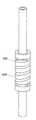
도 1a는 통상적인 플라즈마 챔버 (100) 의 측면도이다. 통상적인 플라즈마 챔버 (100) 는 단일 샤워헤드 타입 상부 전극 (102), 및 기판 (130) 이 플라즈마 (150) 에 의해서 프로세싱되는 동안에 기판 (130) 을 지지하기 위한 기판 지지부 (140) 를 갖는다.1A is a side view of a
도 1b는 통상적인 플라즈마 챔버 (100) 내의 통상적인 상부 전극의 보다 상세한 도면이다. 단일 샤워헤드 타입 상부 전극 (102) 은 몇 개의 층들 (104, 110, 120, 125) 을 포함한다. 표면 층 (104) 은 노출된 플라즈마 표면 (104A) 및 다수의 유출 포트들 (106) 을 포함한다. 노출된 플라즈마 표면 (104A) 은 플라즈마 (150) 에 노출된 표면 층의 표면이다. 유출 포트들 (106) 은 프로세스 가스들의 균일한 분배를 유지하도록 플라즈마 챔버 (100) 에 걸쳐서 실질적으로 균일하게 분포된다.1B is a more detailed view of a typical top electrode within a
표면 층 (104) 후방에 가스 분배 층 (110) 이 존재한다. 가스 분배 층 (110) 은 프로세스 가스들을 균일하게 유출 포트들 (106) 로 표면 층 (104) 에 걸쳐서 분배하도록 다수의 가스 통로들 (112,114) 을 포함한다. 다수의 가스 통로들 (112,114) 은 도시되지 않은 하나 이상의 외부 프로세스 가스 소스들에 연통된다. 다수의 가스 통로들 (112,114) 이 유출 포트들 (106) 각각에 프로세스 가스들을 균일하게 분배하고 이로써 플라즈마 챔버 (100) 전체에 걸쳐서 균일하게 분배하는 것을 보장하기 위해서 다수의 가스 통로들 (112,114) 의 세부 설계에 대한 많은 연구가 이루어지고 있다.There is a
가스 분배 층 (110) 후방에 온도 제어 층 (120) 이 존재한다. 온도 제어 층 (120) 은 엘리먼트들 (122) 을 포함한다. 엘리먼트들 (122) 은 상부 전극 (102) 의 온도를 제어하도록 필요에 따라서 온도 제어 층 (120) 을 냉각 또는 가열시킬 수 있다. 상부 전극 (102) 의 온도는 플라즈마 챔버 (100) 에서 발생하는 플라즈마 프로세싱을 제어하는 일 측면으로서 제어된다. 표면 층 (104) 에 걸쳐서 균일한 온도를 유지하기 위해서 온도 제어 층 (120) 의 세부 설계에 대한 많은 연구가 이루어지고 있다.There is a
공교롭게도, 다양한 이유들로 인해서, 플라즈마 프로세싱은 기판 (130) 의 중앙에서 에지에 걸쳐서 언제나 균일한 것은 아니다. 전술한 바를 고려하면, 기판 (130) 의 중앙으로부터 에지에 걸쳐서 플라즈마 프로세싱을 조작하는 방법 및 시스템이 필요하다.
Coincidentally, for various reasons, plasma processing is not always uniform across the center to edge of the
넓게 말하면, 본 발명은 기판의 중앙에서 에지에 걸쳐서 플라즈마 프로세싱을 조작하는 방법 및 시스템을 제공함으로써 위의 필요들을 채운다. 본 발명은 프로세스, 장치, 시스템, 디바이스, 또는 컴퓨터 판독가능한 매체와 같은 다양한 방식들로 구현될 수 있다. 본 발명의 몇몇 창의적인 실시예들이 이하에서 기술된다.Broadly speaking, the present invention fulfills the above needs by providing a method and system for manipulating plasma processing from the center to the edge of the substrate. The invention may be embodied in various ways such as a process, an apparatus, a system, a device, or a computer-readable medium. Some inventive embodiments of the invention are described below.
일 실시예는 플라즈마 프로세싱 시스템을 제공하며, 이 시스템은 플라즈마 챔버; 및 플라즈마 챔버에 연결된 제어기를 포함한다. 플라즈마 챔버는, 기판 지지부; 및 기판 지지부에 대향하는 상부 전극을 포함하며, 상부 전극은 복수의 동심 가스 주입 존들을 갖는다.One embodiment provides a plasma processing system comprising: a plasma chamber; And a controller coupled to the plasma chamber. The plasma chamber includes a substrate support; And an upper electrode opposite the substrate support, wherein the upper electrode has a plurality of concentric gas injection zones.
복수의 동심 가스 주입 존들 각각은 복수의 가스 피드들 (gas feeds) 을 포함하며, 복수의 가스 피드들은 대응하는 가스 주입 존들에 걸쳐서 (around) 균일하게 분포된다. 제 1 동심 가스 주입 존 내의 제 1 복수의 가스 피드들은 제 2 동심 가스 주입 존 내의 제 2 복수의 가스 피드들과 정렬될 수 있다. 제 1 동심 가스 주입 존 내의 제 1 복수의 가스 피드들은 제 2 동심 가스 주입 존 내의 제 2 복수의 가스 피드들과 시계방향으로 오프셋 (offset) 된다.Each of the plurality of concentric gas injection zones includes a plurality of gas feeds, wherein the plurality of gas feeds are uniformly distributed over the corresponding gas injection zones. The first plurality of gas feeds in the first concentric gas injection zone may be aligned with the second plurality of gas feeds in the second concentric gas injection zone. The first plurality of gas feeds in the first concentric gas injection zone are clockwise offset from the second plurality of gas feeds in the second concentric gas injection zone.
복수의 가스 피드들 중 적어도 하나는 플라즈마 어레스터 (plasma arrestor) 를 포함한다. 플라즈마 어레스터는 플라즈마를 지지하기에는 너무 작은 폭을 갖는 복수의 소형 채널들을 포함한다. 플라즈마 어레스터는 접지 전극을 포함한다.At least one of the plurality of gas feeds includes a plasma arrestor. The plasma arrestor includes a plurality of small channels having a width that is too small to support the plasma. The plasma arrestor includes a ground electrode.
복수의 동심 가스 주입 존들 각각은 복수의 동심 가스 배관 (plenum) 링들을 포함한다. 대응하는 동심 가스 주입 존 내의 상기 동심 가스 배관 링들은 복수의 가스 채널들에 의해서 함께 연통된다. 플라즈마 프로세싱 시스템은 복수의 동심 가스 주입 존들 각각은 복수의 유출 포트들을 포함할 수 있다. 플라즈마 프로세싱 시스템은 내측 상부 전극에 접속된 RF 소스를 더 포함할 수 있다.Each of the plurality of concentric gas injection zones includes a plurality of concentric gas plenum rings. The concentric gas pipe rings in the corresponding concentric gas injection zones are communicated together by a plurality of gas channels. The plasma processing system may include a plurality of outflow ports each of the plurality of concentric gas injection zones. The plasma processing system may further comprise an RF source connected to the inner top electrode.
다른 실시예는 플라즈마 프로세싱 시스템을 제공하며, 이 시스템은 플라즈마 챔버; 및 플라즈마 챔버에 연결된 제어기를 포함한다. 플라즈마 챔버는, 기판 지지부; 및 기판 지지부에 대향하는 상부 전극을 포함하며, 상부 전극은 복수의 동심 가스 주입 존들 (gas injection zones) 을 갖는다. 복수의 동심 가스 주입 존들 각각은 복수의 가스 피드들 (gas feeds) 을 포함한다. 복수의 가스 피드들은 대응하는 가스 주입 존들에 걸쳐서 (around) 균일하게 분포된다. 복수의 가스 피드들 중 적어도 하나는 플라즈마 어레스터 (plasma arrestor) 를 포함한다. 제 1 동심 가스 주입 존 내의 제 1 복수의 가스 피드들은 제 2 동심 가스 주입 존 내의 제 2 복수의 가스 피드들과 시계방향으로 오프셋 (offset) 된다.Another embodiment provides a plasma processing system comprising: a plasma chamber; And a controller coupled to the plasma chamber. The plasma chamber includes a substrate support; And an upper electrode opposite the substrate support, wherein the upper electrode has a plurality of concentric gas injection zones. Each of the plurality of concentric gas injection zones includes a plurality of gas feeds. The plurality of gas feeds are uniformly distributed over the corresponding gas injection zones. At least one of the plurality of gas feeds includes a plasma arrestor. The first plurality of gas feeds in the first concentric gas injection zone are clockwise offset from the second plurality of gas feeds in the second concentric gas injection zone.
또 다른 실시예는 다수의 동심 가스 주입 존들을 갖는 상부 전극을 사용하여서 에칭 레이트를 선택하는 방법을 제공하며, 이 방법은 플라즈마 챔버 내에 플라즈마를 생성하는 단계; 제 1 동심 가스 주입 존 내의 제 1 에칭 레이트를 감소시키는 단계로서, 상기 제 1 동심 가스 주입 존 내에 튜닝 가스 (tuning gas) 를 주입하는 단계를 포함하는, 상기 제 1 동심 가스 주입 존 내의 제 1 에칭 레이트를 감소시키는 단계; 및 제 2 동심 가스 주입 존 내의 제 2 에칭 레이트를 감소시키는 단계로서, 상기 제 2 동심 가스 주입 존 내에 튜닝 가스 (tuning gas) 를 주입하는 단계를 포함하는, 상기 제 2 동심 가스 주입 존 내의 제 2 에칭 레이트를 감소시키는 단계를 포함한다.Yet another embodiment provides a method of selecting an etch rate using an upper electrode having a plurality of concentric gas injection zones, the method comprising: generating a plasma in a plasma chamber; A method of reducing a first etch rate in a first concentric gas injection zone, comprising: injecting a tuning gas into the first concentric gas injection zone, wherein the first etch rate in the first concentric gas injection zone Reducing the rate; And reducing a second etch rate in the second concentric gas injection zone, wherein the step of injecting a tuning gas into the second concentric gas injection zone further comprises: And reducing the etch rate.
제 1 동심 가스 주입 존 내의 제 1 에칭 레이트를 감소시키는 단계는, 제 1 동심 가스 주입 존 내의 제 1 기판 온도 또는 제 1 동심 가스 주입 존 내의 제 1 상부 전극 온도 중 적어도 하나를, 제 2 동심 가스 주입 존 내의 제 2 기판 온도 또는 제 2 동심 가스 주입 존 내의 제 2 상부 전극 온도 중 적어도 하나보다 높은 온도로 설정하는 단계를 포함한다.The step of reducing the first etching rate in the first concentric gas injection zone may include at least one of the first substrate temperature in the first concentric gas injection zone or the first upper electrode temperature in the first concentric gas injection zone, To a temperature higher than at least one of a second substrate temperature in the injection zone or a second upper electrode temperature in the second concentric gas injection zone.
제 1 동심 가스 주입 존 내의 제 1 에칭 레이트를 증가시키는 단계는 제 1 동심 가스 주입 존 내의 제 1 기판 온도 또는 제 1 동심 가스 주입 존 내의 제 1 상부 전극 온도 중 적어도 하나를, 제 2 동심 가스 주입 존 내의 제 2 기판 온도 또는 제 2 동심 가스 주입 존 내의 제 2 상부 전극 온도 중 적어도 하나보다 낮은 온도로 설정하는 단계를 포함한다.The step of increasing the first etching rate in the first concentric gas injection zone may include at least one of the first substrate temperature in the first concentric gas injection zone or the first upper electrode temperature in the first concentric gas injection zone, To a temperature lower than at least one of a second substrate temperature in the zone or a second upper electrode temperature in the second concentric gas injection zone.
튜닝 가스는 프로세싱되는 기판의 표면에서의 탄소/불소 비를 감소시킨다. 튜닝 가스는 산소 또는 다른 적합한 튜닝 가스들을 포함할 수 있다.The tuning gas reduces the carbon / fluorine ratio at the surface of the substrate being processed. The tuning gas may comprise oxygen or other suitable tuning gases.
본 발명의 다른 양태들 및 장점들은 본 발명의 원리들을 예시적으로 설명하는 다음의 상세한 설명을 첨부 도면들과 함께 취함으로써 명백해질 것이다.
Other aspects and advantages of the present invention will become apparent from the following detailed description, taken in conjunction with the accompanying drawings, which illustrate, by way of example, the principles of the invention.
본 발명은 첨부 도면들과 함께 다음의 상세한 설명 부분에 의해서 용이하게 이해될 것이다.
도 1a는 통상적인 플라즈마 챔버의 측면도이다.
도 1b는 플라즈마 챔버 내의 통상적인 상부 전극의 보다 상세한 도면이다.
도 2는 본 발명의 실시예들에 따른, 플라즈마 챔버이다.
도 3a은 본 발명의 실시예들에 따른 플라즈마 챔버의 에지 영역의 개략도이다.
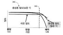
도 3b는 본 발명의 실시예들에 따른, 이온들 및 중성종들의 밀도의 그래프이다.
도 3c는 본 발명의 실시예들에 따른, 기판의 반경에 걸친 상대적 에칭 레이트들의 그래프이다.
도 3d는 본 발명의 실시예들에 따른, 플라즈마 챔버 상단의 일부의 개략도이다.
도 4a는 본 발명의 실시예들에 따른, 이중 온도 존 상부 전극을 사용하여서 에지 에칭 레이트를 선택할 시에 수행되는 방법 동작들을 예시하는 흐름도이다.
도 4b는 본 발명의 실시예들에 따른, 상부 전극의 설정점 온도 (set point temperature) 를 유지할 시에 수행되는 방법 동작들을 예시하는 흐름도이다.
도 5a 및 도 5b는 본 발명의 실시예들에 따른, 다중 존 가스 주입 상부 전극의 개략도들이다.
도 5c는 본 발명의 실시예들에 따른, 다수의 가스 주입 존들 각각에서의 튜닝 가스 주입들의 효과의 그래프다.
도 5d 및 도 5e는 본 발명의 실시예들에 따른, 튜닝 가스 및 프로세스 가스의 상대적 밀도들의 그래프들이다.
도 6은 본 발명의 실시예들에 따른, 다중 존 가스 주입 상부 전극을 갖는 플라즈마 챔버의 단면도이다.
도 7a는 본 발명의 실시예들에 따른, 분배된 가스 공급 피드 (feed) 의 개략도이다.
도 7b 내지 도 7f는 본 발명의 실시예들에 따른, 플라즈마 어레스터 (arrestor) 의 개략도이다.
도 8은 본 발명의 실시예들에 따른, 분포된 가스 존들을 사용하여서 에지 에칭 레이트를 선택할 시에 수행되는 방법 동작들을 예시하는 흐름도이다.
도 9는 본 발명의 실시예들에 따른 컴퓨터 시스템의 단순화된 개략도이다.
도 10a는 발명의 실시예들에 따른, 가열된 에지 링의 개략도이다.
도 10b 및 도 10c는 발명의 실시예들에 따른, 캠 록 (cam lock) 의 개략도들이다.
도 10d 및 도 10e는 발명의 실시예들에 따른, 가열기들로의 전기적 접속부들의 개략도들이다.
도 10f는 발명의 실시예들에 따른, 광학적 온도 센서의 개략도이다.The present invention will be readily understood by the following detailed description together with the accompanying drawings.
1A is a side view of a conventional plasma chamber.
1B is a more detailed view of a typical top electrode in a plasma chamber.
Figure 2 is a plasma chamber, in accordance with embodiments of the present invention.
3A is a schematic diagram of an edge region of a plasma chamber in accordance with embodiments of the present invention.
Figure 3B is a graph of the density of ions and neutral species, in accordance with embodiments of the present invention.
3C is a graph of relative etch rates over a radius of the substrate, in accordance with embodiments of the present invention.
Figure 3d is a schematic view of a portion of the top of a plasma chamber, in accordance with embodiments of the present invention.
4A is a flow diagram illustrating method operations performed in selecting an edge etch rate using a dual temperature zone top electrode, in accordance with embodiments of the present invention.
4B is a flow diagram illustrating method operations performed in maintaining the set point temperature of the top electrode, in accordance with embodiments of the present invention.
Figures 5A and 5B are schematic diagrams of a multi-zone gas injection top electrode, in accordance with embodiments of the present invention.
Figure 5c is a graph of the effect of tuning gas injections in each of a plurality of gas injection zones, in accordance with embodiments of the present invention.
5D and 5E are graphs of relative densities of tuning gas and process gas, according to embodiments of the present invention.
6 is a cross-sectional view of a plasma chamber having a multi-zone gas injection top electrode, in accordance with embodiments of the present invention.
7A is a schematic diagram of a distributed gas feed feed, in accordance with embodiments of the present invention.
7B-7F are schematic diagrams of a plasma arrestor, in accordance with embodiments of the present invention.
8 is a flow diagram illustrating method operations performed in selecting an edge etch rate using distributed gas zones, in accordance with embodiments of the present invention.
Figure 9 is a simplified schematic diagram of a computer system in accordance with embodiments of the present invention.
10A is a schematic view of a heated edge ring, in accordance with embodiments of the invention.
Figures 10B and 10C are schematic diagrams of a cam lock, in accordance with embodiments of the invention.
10D and 10E are schematic diagrams of electrical connections to the heaters, in accordance with embodiments of the invention.
Figure 10f is a schematic diagram of an optical temperature sensor, in accordance with embodiments of the invention.
기판의 중앙에서 에지에 걸쳐서 플라즈마 프로세싱을 조작하는 방법 및 시스템에 대한 몇몇 예시적인 실시예들이 이제 기술될 것이다. 본 발명은 본 명세서에서 기술된 특정 세부사항 전부 또는 일부 없이도 실시될 수 있음이 본 기술 분야의 당업자에게 자명하다.Several exemplary embodiments of a method and system for manipulating plasma processing from the center to the edge of a substrate will now be described. It will be apparent to those skilled in the art that the present invention may be practiced without some or all of the specific details described herein.
기판의 중앙에서 에지에 걸쳐서 플라즈마 프로세싱을 조작하는 일 방식은 기판의 중앙 (130A) 으로부터 에지 (130B) 에 걸쳐서 상부 전극의 온도를 변화시키는 것이다. 기판의 중앙 (130A) 에서 에지 (130B) 에 걸쳐서 플라즈마 프로세싱을 조작하는 다른 방식은 기판의 중앙 (130A) 으로부터 에지 (130B) 에 걸쳐서 프로세스 가스 농도를 조작하는 것이다.One way of manipulating the plasma processing from the center to the edge of the substrate is to vary the temperature of the upper electrode from the
도 2는 본 발명의 실시예들에 따른, 플라즈마 챔버 (200) 이다. 도 2의 챔버는 각기 RF 주파수 f1, f2, f3를 갖는 RF 전력 소스들 (220, 222 및 224) 을 포함하며, 이 RF 전력 소스들은 대응하는 매칭 네트워크들을 통해서 하단 전극 (108) 에 접속된다. 상부 전극 (201) 은, 스위치 (244) 및 매칭 네트워크 (246) 를 통해서, RF 주파수 f4를 갖는 제 4 RF 전력 소스 (242) 에 접속된다.Figure 2 is a
또한, 챔버는 상부 전극 (201) 을 매칭 네트워크 (246) 를 통해서 접지 접위 또는 RF 전력 소스 (242) 에 접속시키는 스위치 (244) 를 포함한다. 제 1 가열기 (218) 가 상부 전극 (201) 위에 위치하며, 제 2 가열기 (216) 가 접지 전극 (248) 위에 위치한다. 이 가열기들은 알루미늄 질화물 재료 층에 의해서 상부 전극 (201) 및 접지 전극으로부터 격리되지만, 다른 절연체들이 이러한 격리를 위해서 또한 사용될 수도 있다. 가열기 (216) 는 접지 전극의 외측 구역 내의 온도를 제어하고, 가열기 (218) 는 상부 전극 (201) 의 온도를 제어한다. 각 가열기는 기판 프로세싱 동작 동안에 독립적으로 턴 온 또는 언 오프되도록 동작가능하다.The chamber also includes a
상부 전극의 온도를 제어하는 것은 챔버의 응답을 조절하는데 사용될 수 있다. 그러나, 이러한 온도를 제어하는 것은 온도가 신속하게 변할 수 있다는 한계를 갖는다. 따라서, 온도 제어는 챔버 내의 변화에 대한 저속 응답을 제공한다. 상부 전극 (201) 의 온도 제어를 사용하여서 각 기판-프로세싱 동작을 제어하는 것은 용이하지 않다. 또한, 챔버 (200) 내에서 실리콘 표면들에 인가될 수 있는 온도의 상한치가 존재한다.Controlling the temperature of the top electrode can be used to adjust the response of the chamber. However, controlling such a temperature has a limitation that the temperature can be changed rapidly. Thus, temperature control provides a slow response to changes in the chamber. It is not easy to control each substrate-processing operation using the temperature control of the
웨이퍼 프로세싱 장치는 시스템 제어기 (202), 상부 전극 전력 제어기 (206), 가열기 제어기 (208) 및 각기 주파수 f1, f2, f3용 전력 제어기들 (210, 212 및 214) 을 더 포함한다. 시스템 제어기 (202) 는 챔버 상에서 수행되는 상이한 동작들에 대한 인스트럭션들을 포함하는 플라즈마 레시피 (204) 를 수신한다. 웨이퍼 프로세싱은 다수의 동작들로 수행될 수 있으며, 각 동작은 챔버 내의 상이한 설정사항들을 요구한다. 예를 들어서, 일 동작 시에, 모든 4 개의 RF 전력 소스들은 턴 온되는데 반해서, 다른 동작에서는, 오직 3 개, 또는 2 개 또는 1 개의 RF 전력 소스만이 턴 온된다.The wafer processing apparatus further includes a
레시피 (204) 에 기초하여서, 시스템 제어기는 어느 RF 소스들이 턴 온되거나 턴 오프되는지, 이들의 전압 및 전력 설정사항들, 스위치 (244) 설정사항, 가열기들 (216,218) 설정사항들, 챔버 내에서 사용되는 가스들, 챔버 상의 압력, 웨이퍼-프로세싱 동작 기간 등을 포함하는 챔버의 동작 파라미터들을 설정한다. 일 실시예에서, 시스템 제어기 (202) 는 상부 전극에 대한 전력 구성을 위한 인스트럭션들을 상부 전극 전력 제어기 (206) 에 전송하며, 이러한 인스트럭션들은 상부 전극을 RF 전력 또는 접지로 접속시키도록 스위치 (244) 를 설정하기 위한 인스트럭션들 및 RF 전력 소스 (242) 를 턴 온 또는 턴 오프시키기 위한 인스트럭션들 및 RF 전력 소스 (242) 에 대한 전력 레벨을 설정하기 위한 인스트럭션들을 포함한다.Based on the
시스템 제어기 (202) 는 상부 전극 (201) 의 온도를 조절하도록 가열기 제어기 (205) 와 인터페이싱한다. 가열기 제어기 (208) 는 상부 전극 (201) 의 온도를 제어하도록 가열기들 (216,218) 을 조절한다. 온도 센서 (미도시) 가 상부 전극의 하나 이상의 지점들에서 상부 전극 (201) 의 온도에 대한 정보를 가열기 제어기 (208) 에 제공한다. 이로써, 가열기 제어기 (208) 는 웨이퍼 프로세싱 동안에 목표 온도를 달성하기 위해서 가열기들을 턴 온 또는 턴 오프시킴으로써 상부 전극 (201) 상의 온도를 조절할 수 있다.The
시스템 제어기 (202) 는 또한 전력 제어기들 (210, 212 및 214) 과 인터페이싱하며, 전력 제어기들은 대응하는 RF 전력 소스 (210, 222 또는 224) 가 턴 온 또는 턴 오프되는지를 조정하며, 해당 전력 소스가 턴 온되면, 그 전력 설정사항을 설정한다. 일 실시예에서, RF 전력 소스 (242) 의 주파수는 400 kHz이다. 다른 실시예에서, 이 주파수는 400 kHz 내지 2 MHz 범위이며, 또 다른 실시예에서는 이 주파수는 100 kHz 내지 10 MHz 범위이다. 몇몇 동작들에서, 3 개의 하단 RF 전력 소스들은 동시에 턴 온되지 않으며 이는 상단 RF 전력에서 보다 높은 주파수를 갖게 한다. 일 실시예에서, 상단 주파수 f4는 챔버 상의 공진을 피하기 위해서 하단 주파수들 f1, f2, f3과 상이하다.The
일 실시예에서, 챔버 내의 압력은 20 mTorr 내지 60 mTorr 값을 갖는다. 다른 실시예에서, 상단 전력 소스의 전압은 수백 볼트 (예를 들어서, 100 V 내지 2000 V 이상) 범위에 있을 수 있으며, 하단 전력 소스들의 전압은 6000 V 이상일 수 있다. 일 실시예에서, 전압은 1000 V이다. 다른 실시예에서, 상단 전력 소스의 전압은 100 V 내지 600 V 값을 가지며, 하단 전력 소스의 전압은 1000 V 내지 6000 V 값을 갖는다. 상단 챔버 및 하단 챔버 내의 압력은 10 mTorr 내지 500 mTorr 값을 가질 수 있다. 일 실시예에서, 챔버는 15 mTorr 압력에서 동작한다.In one embodiment, the pressure in the chamber has a value of 20 mTorr to 60 mTorr. In other embodiments, the voltage of the upper power source may be in the range of hundreds of volts (e.g., 100 V to 2000 V or higher), and the voltage of the lower power sources may be higher than 6000 V. In one embodiment, the voltage is 1000 volts. In another embodiment, the voltage of the upper power source has a value between 100 V and 600 V, and the voltage of the lower power source has a value between 1000 V and 6000 V. The pressure in the upper chamber and the lower chamber may have values from 10 mTorr to 500 mTorr. In one embodiment, the chamber operates at 15 mTorr pressure.
도 2에 예시된 실시예는 예시적임이 주목된다. 다른 실시예들은 상이한 타입의 챔버들, 상이한 주파수들, 레시피에 기초한 챔버 구성에 대한 다른 타입의 조절, 챔버 내의 상이한 압력, 등을 사용할 수 있다. 예를 들어서, 일 실시예에서, 챔버는 CCP 플라즈마 챔버이다. 또한, 반도체 웨이퍼 프로세싱 장치 내의 상술한 모듈들 중 몇몇은 단일 모듈로 결합되거나, 단일 모듈의 기능이 복수의 모듈들에 의해서 수행될 수도 있다. 예를 들어서, 일 실시예에서, 전력 제어기들 (210, 212, 및 214) 은 시스템 제어기 (202) 내에 통합될 수 있지만, 다른 구성도 역시 가능하다. 도 2에 예시된 실시예는 한정적으로 해석되지 말고 예시적으로 해석되어야 한다.It is noted that the embodiment illustrated in FIG. 2 is exemplary. Other embodiments may use different types of chambers, different frequencies, different types of adjustments to the recipe based chamber configuration, different pressures in the chamber, and the like. For example, in one embodiment, the chamber is a CCP plasma chamber. In addition, some of the modules described above in the semiconductor wafer processing apparatus may be combined into a single module, or the function of a single module may be performed by a plurality of modules. For example, in one embodiment, the
이중 온도 존 상부 전극Double temperature zone upper electrode
도 3a은 본 발명의 실시예들에 따른 플라즈마 챔버 (200) 의 에지 영역의 개략도이다. 상부 전극 (201) 은 기판 에지 영역 (130B) 위의 영역들 (312A) 위의 내측 가열기 (218) 에 열적으로 연결된다. 플라즈마 한정 구조체 (252) 는 기판 에지 영역 (130B) 을 넘어서 외측으로 연장된다. 플라즈마 한정 구조체 (252) 는 다수의 한정 링들 (254) 을 포함한다.3A is a schematic diagram of an edge region of a
기판 지지부 (140) 는 에지 링 (205) 을 포함한다. 에지 링 (205) 은 에지 링을 목표 에지 링 온도로 가열 또는 냉각할 수 있는 에지 링 온도 제어 메카니즘을 포함한다. 에지 링 (205) 은 기판 에지 영역 (130B) 에 인접하고 그 외측에 존재한다. 에지 링 (205) 은 에지 링 (307) 에 의해서 플라즈마로부터 전기적으로 분리된다.The
플라즈마 한정 구조체 (252) 는 플라즈마 챔버의 상부 부분으로부터 하향 돌출된 돌출부 (310) 를 또한 포함한다. 이 돌출부 (310) 는 외측 가열기 (216) 에 열적으로 연결된다.
절연체 (250) 가 상부 전극 (201) 을 돌출부 (310) 로부터 그리고 내측 가열기 (218) 를 외측 가열기 (216) 로부터 전기적으로 그리고 열적으로 분리한다. 내측 가열기 (218) 는 상부 전극 (201) 을 제 1 목표 온도 T1 (즉, 내측 전극 온도) 로 가열할 수 있다. 외측 가열기 (216) 는 돌출부 (310) 를 제 2 목표 온도 T2 (즉, 외측 전극 온도) 로 가열할 수 있다. 마찬가지로, 에지 링 (205) 이 제 3 목표 온도 T3 (즉, 에지 링 온도) 로 가열될 수 있다. 기판 (130) 이 제 4 목표 온도 T4 (즉, 기판 온도) 로 가열될 수 있다.An
내측 영역 (312A) 및 외측 영역 (312B) 에서의 중성 분자들 (302) 및 이온들 (304) 의 밀도가 상대적 온도들 (T1, T2, T3 및 T4) 에 의해서 선택될 수 있다. 중성 분자들 (302) 은 에칭된 표면과 이온들 (304) 간의 반응성을 완충시킬 수 있다. 중성 분자들 (302) 은 상대적 온도들 (T1, T2, T3 및 T4) 의 열적 구배 시에 확산되고 이 상대적 온도들의 최저 온도 표면에 부착되는 경향이 있다. 중성 분자들 (302) 과 이온들 (304) 의 상대적 밀도가 에칭 레이트를 선택하도록 조작될 수 있다.The density of the
예시적으로, T1 > T2이면, 중성 분자들 (302) 의 상대적 밀도는 기판 (130) 의 에지 영역 (130B) 상에서 외측 플라즈마 영역 (312B) 에 비해서 내측 플라즈마 영역 (312A) 내에서 증가할 수 있다. 이로써, 기판 (130) 의 에지 영역 (130B) 상에서 이온들 (304) 의 반응성이 감소한다. 이러한 감소된 이온들 (304) 반응성은 기판 (130) 의 에지 영역 (130B) 의 에칭 레이트가 그에 따라서 감소되게 한다.Illustratively, if T1 > T2, the relative density of the
마찬가지로, T2 > T1이면, 중성 분자들 (302) 의 상대적 밀도는 기판 (130) 의 에지 영역 (130B) 상에서 외측 플라즈마 영역 (312B) 에 비해서 내측 플라즈마 영역 (312A) 내에서 감소할 수 있다. 이로써, 기판 (130) 의 에지 영역 (130B) 상에서 이온들 (304) 의 반응성이 증가한다. 이러한 증가된 이온들 (304) 반응성은 기판 (130) 의 에지 영역 (130B) 의 에칭 레이트가 그에 따라서 증가되게 한다.Likewise, if T2 > T1, the relative density of the
이로써, 각각의 플라즈마 영역들 (312A,312B) 내의 각각의 온도를 선택함으로써, 대응하는 에칭 레이트가 기판 (130) 의 에지 영역 (130B) 에서 증가하거나 감소할 수 있다.Thus, by selecting the respective temperature in each of the
도 3b는 본 발명의 실시예들에 따른, 이온들 (304) 및 중성종들 (302) 의 밀도의 그래프 (350) 이다. 그래프 (350) 는 수평 축이 기판의 반경이며 수직 축이 이온들 (304) 및 중성종들 (302) 의 상대적 밀도이다.Figure 3B is a
도 3c는 본 발명의 실시예들에 따른, 기판 (130) 의 반경에 걸친 상대적 에칭 레이트들의 그래프 (370) 이다. 그래프 (370) 는 수평 축이 기판의 반경이며 다수의 에칭 반복의 에칭 레이트들이 수직 축에 나타난다.FIG. 3C is a
기판 (130) 의 중앙 영역 (130A) 내에서, 이온들 (304) 및 중성종들 (302) 의 상대적 밀도는 대략적으로 동일하며, 대응하는 에칭 레이트는 기판의 이 동일한 부분에서는 대략적으로 동일하다.Within the
기판 (130) 의 에지 영역 (130B) 으로 향하면, 상대적 밀도는 강하 라인 (drop-off line) (352) 에서 변하는 경향이 있다. 상술한 바와 같이, 상대적 온도들 (T1, T2, T3) 을 조작하는 것은 강하 라인 (352) 을 그래프 상에서 우측 또는 좌측으로 이동시킬 수 있다. 이상적으로는, 상술한 바와 같이, 상대적 온도들 (T1, T2, T3) 을 조작하는 것은 강하 라인 (352) 을 기판 (130) 의 에지 영역 (130B) 을 넘어서 우측으로 이동시킬 수 있다.The relative density tends to change in the drop-
도 3d는 본 발명의 실시예들에 따른, 플라즈마 챔버 상단의 일부의 개략도이다. 상단은 내측 가열기 (218), 외측 가열기 (216), 접지 전극 (248), 가스 분배 플레이트 (610) 및 절연체 플레이트 (382) (알루미늄 질화물 또는 다른 적합한 절연체) 를 포함한다. 가스 분배 플레이트 (610) 는 인가된 RF 신호를 가지며, 따라서 통상적인 써모커플들은 효과적으로 기능하기 위해서 필터 네트워크들을 필요로 한다. 이 때문에, 가스 분배 플레이트 (610) 의 온도를 모니터링하기 위해서 광학적 온도 센서 (384) 가 사용될 수 있다.Figure 3d is a schematic view of a portion of the top of a plasma chamber, in accordance with embodiments of the present invention. The top includes an
광학적 온도 센서 (384) 는 가스 분배 플레이트 (610) 의 적합한 광학적 뷰 (optical view) 을 제공하는 임의의 배향 및 위치로 위치할 수 있다는 것이 이해되어야 한다. 광학적 온도 센서 (384) 는 절연체 플레이트 (382) 를 통해서 가스 분배 플레이트의 온도를 모니터링할 수 있다. 접지 전극 (248) 이 또한 플레이트 가열기를 포함할 수 있다.It should be appreciated that the
내측 가열기 (218), 외측 가열기 (216), 가열된 에지 링 (205) 및 정전 척 (140) 내의 가열 및 냉각 시스템들은 플라즈마 챔버 내에서 열적 램프 업 시간 (thermal ramp up time) 을 줄이도록 개별적으로 그리고 서로 조합하여서 사용될 수 있다. 내측 가열기 (218), 외측 가열기 (216), 가열된 에지 링 (205) 및 정전 척 (140) 내의 가열 및 냉각 시스템들은 플라즈마 프로세싱 동안에 통상적으로 플라즈마 챔버의 다양한 부분들에서 발생하는 중간의 부분적 냉각을 최소화하고 심지어 실질적으로 제거하도록 개별적으로 그리고 서로 조합하여서 사용될 수 있다. 이러한 중간의 부분적 냉각을 줄이거나 제거하는 것은 프로세싱 속도를 개선하며 플라즈마 챔버 내의 목표된 표면들에 걸쳐서 시간에 따라서 보다 일정한 온도로 플라즈마 챔버를 유지할 수 있다. 이러한 중간의 부분적 냉각을 줄이거나 제거하는 것은, 고온 스팟 (spot) 및 인터벌 (interval) 및 저온 스팟 및 인터벌이 챔버 내에 존재하는 생성물들에 의해서 다양한 가스들 및 플라즈마의 분압 (partial pressure) 에 영향을 줄 수 있기 때문에, 화학적 프로세스들의 일관성을 개선시킨다.The heating and cooling systems within the
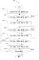
도 4a는 본 발명의 실시예들에 따른, 이중 (dual) 온도 존 (zone) 상부 전극을 사용하여서 에지 에칭 레이트를 선택할 시에 수행되는 방법 동작들 (400) 을 예시하는 흐름도이다. 본 명세서에서 예시된 동작들은 예시적이며, 따라서 몇몇 동작들은 하위 동작들을 가질 수 있으며, 다른 실례에서는, 본 명세서에서 기술된 특정 동작들은 예시된 동작들에 포함되지 않을 수 있다. 이를 염두하고, 방법 및 동작들 (400) 이 이제 기술될 것이다.4A is a flow diagram illustrating
동작 (405) 에서, 플라즈마 (260) 가 플라즈마 챔버 (262) 내에서 생성된다. 동작 (410) 에서, 에지 영역 (130B) 위의 에칭 레이트를 감소시킬지의 여부를 결정하는 질의가 행해진다. 에지 영역 (130B) 위의 에칭 레이트가 감소될 것이면, 이 방법 동작들은 동작 (415) 에서 계속된다. 에지 영역 (130B) 위의 에칭 레이트가 감소되지 않을 것이면, 이 방법 동작들은 동작 (420) 에서 계속된다.At
동작 (415) 에서, 온도 T1 및/또는 T4가 온도 T2 및 T3보다 높게 되게 조절되고, 이 방법 동작들은 동작 (430) 에서 계속된다.At
동작 (420) 에서, 에지 영역 (130B) 위의 에칭 레이트를 증가시킬지의 여부를 결정하는 질의가 행해진다. 에지 영역 (130B) 위의 에칭 레이트가 증가될 것이면, 이 방법 동작들은 동작 (425) 에서 계속된다. 에지 영역 (130B) 위의 에칭 레이트가 증가되지 않을 것이면, 이 방법 동작들은 동작 (430) 에서 계속된다.At
동작 (425) 에서, 온도 T2 및/또는 T3가 온도 T1 및 T4보다 높게 되게 조절되고, 이 방법 동작들은 동작 (430) 에서 계속된다.At
동작 (430) 에서, 에칭 프로세싱을 완료할지의 여부를 결정하는 질의가 행해진다. 에칭 프로세스가 완료될 것이면, 이 방법 동작들은 종료될 수 있다. 에칭 프로세스가 완료되지 않을 것이면, 이 방법 동작들은 상술한 바와 같은 동작 (410) 에서 계속된다.At
상부 전극 (201) 의 이중 존 온도 제어를 갖는 다른 양태는 상부 전극이 인가된 RF를 가지며 이로써 열이 상부 전극에서 생성되고 RF가 인가되지 않을 때에는 냉각되는 경우이다. 가열기들 (218,216) 이 상부 전극 (201) 의 이중 존 온도 제어를 제공하며 이로써 상부 전극 (201) 의 중앙 부분은 RF가 인가된 때에는 냉각되게 하고 RF가 인가되지 않은 때에는 가열되게 하여서 목표 설정점 온도가 유지되게 한다.Another embodiment with dual zone temperature control of the
본 발명의 다른 양태는 이중 존 온도 제어 상부 전극이 제공하기 위해서 (예를 들어서, 세정을 위해서) 전극 (201) 의 나머지 부분으로부터 제거가능한 상부 전극 (201) 의 비도전성 표면 (201A) 을 가질 수 있는 것이다.Another aspect of the present invention is to provide a non-conductive surface 201A of a removable
도 4b는 본 발명의 실시예들에 따른, 상부 전극 (201) 의 설정점 온도 (set point temperature) 를 유지할 시에 수행되는 방법 동작들 (405) 을 예시하는 흐름도이다. 본 명세서에서 예시된 동작들은 예시적이며, 따라서 몇몇 동작들은 하위 동작들을 가질 수 있으며, 다른 실례에서는, 본 명세서에서 기술된 특정 동작들은 예시된 동작들에 포함되지 않을 수 있다. 이를 염두하고, 방법 및 동작들 (450) 이 이제 기술될 것이다.4B is a flow chart illustrating
동작 (452) 에서, 플라즈마 (260) 가 플라즈마 챔버 (262) 내에서 생성된다. 동작 (454) 에서, RF 전력이 상부 전극 (201) 에 인가될지의 여부를 결정하는 질의가 행해진다. RF 전력이 상부 전극 (201) 에 인가될 것이면, 이 방법 동작들은 동작 (456) 에서 계속된다. RF 전력이 상부 전극 (201) 에 인가되지 않을 것이면, 이 방법 동작들은 동작 (458) 에서 계속된다.At
동작 (456) 에서, 설정점 온도를 유지하도록 온도 T1이 감소되고, 이 방법 동작들은 동작 (460) 에서 계속된다. 동작 (458) 에서, 설정점 온도를 유지하도록 온도 T1이 증가되고, 이 방법 동작들은 동작 (460) 에서 계속된다.At
동작 (460) 에서, 에칭 프로세싱을 완료할지의 여부를 결정하는 질의가 행해진다. 에칭 프로세스가 완료될 것이면, 이 방법 동작들은 종료될 수 있다. 에칭 프로세스가 완료되지 않을 것이면, 이 방법 동작들은 상술한 바와 같은 동작 (454) 에서 계속된다.At
다중 존 가스 주입 상부 전극Multi-zone gas injection upper electrode
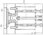
기판의 중앙 (130A) 에서 에지 (130B) 에 걸쳐서 플라즈마 프로세싱을 조작하는 다른 방식은 기판의 중앙으로부터 에지에 걸쳐서 방사상으로 프로세스 가스 농도를 조절하는 것이다. 상부 전극 (501) 으로부터의 다중-존 가스 주입은 튜닝 가스 (tuning gas) (예를 들어서, 산소 가스 또는 다른 튜닝 가스) 가 기판 (130) 의 중앙으로부터 방사상 외측으로 상이한 존들 내로 주입되게 한다. 튜닝 가스는 기판 (130) 의 표면에서의 탄소/불소 비를 변화시키고 이로써 이온 밀도 및 이에 대응하는 에칭 레이트를 변화시킨다.Another way to manipulate plasma processing from the
본 명세서에서 기술되는 예시적인 실시예는 상부 전극 (501) 에서 3 개의 가스 주입 존들을 포함하지만, 3 개보다 많은 가스 존들 (예를 들어서, 4 개 또는 그 이상의 존들) 이 사용될 수도 있음이 이해되어야 한다.It should be understood that the exemplary embodiment described herein includes three gas injection zones at the
도 5a 및 도 5b는 본 발명의 실시예들에 따른, 다중 존 가스 주입 상부 전극 (501) 의 개략도들 (500, 550) 이다. 다중 존 가스 주입 상부 전극 (501) 은 가스 주입 존들 (502, 504, 506) 을 포함한다. 가스 주입 존들 (502, 504, 506) 은 동심이다.Figures 5A and 5B are schematic diagrams 500 and 550 of a multi-zone gas
중앙 가스 주입 존 1 (502) 은 중앙 가스 공급 피드 (552) 를 갖는다. 동심 가스 주입 존들 (504, 506) 각각은 각각의 원주를 따라서 실질적으로 균일하게 분포된 각각의 가스 공급 피드들을 갖는다. 예시적으로, 가스 주입 존 2 (504) 은 4 개의 가스 공급 피드들 (554) 를 가지며, 이 피드들은 중앙 및 스포크 (central and spoke) 분포 매니폴드 (manifold) 에 의해서 공급된다. 마찬가지로, 가스 주입 존 3 (506) 은 8 개의 가스 공급 피드들 (556) 를 가지며, 이 피드들은 중앙 및 스포크 (central and spoke) 분포 매니폴드 (manifold) 에 의해서 공급된다.Central
균일하게 분포된 가스 공급 피드들 (554, 556) 은 그들의 각각의 가스 주입 존들 (504,506) 내에서 정렬될 수 있다. 이와 달리, 균일하게 분포된 가스 공급 피드들 (554, 556) 은 그들의 각각의 가스 주입 존들 (504,506) 내에서 오프셋될 수 있다. 가스 공급 피드들 (554, 556) 의 개수는 각 가스 주입 존 (504,506) 에서 동일하거나 각 존에서 상이할 수 있다.The uniformly distributed gas feeds 554 and 556 may be aligned within their respective
가스 주입 존들 (502, 504, 506) 각각은 하나 이상의 동심 가스 배관 (plenum) 링들 (562, 564, 566) 을 포함할 수 있다. 동심 가스 배관 (plenum) 링들 (562, 564, 566) 은 각각의 가스 주입 존들 (502, 504, 506) 내에서 다수의 가스 채널들 (572, 574, 576) 에 의해서 서로 연통된다. 각각의 가스 주입 존들 (502, 504, 506) 은 상부 전극의 표면을 통해서 플라즈마 존 내로의 다수의 유출 포트들 (532, 534, 536) 을 포함한다.Each of the
도 5c는 본 발명의 실시예들에 따른, 다수의 가스 주입 존들 (502, 504, 506) 각각에서의 튜닝 가스 주입들의 효과의 그래프 (520) 이다. 그래프 (521) 는 가스 주입 존 1 (502) 내에 주입된 튜닝 가스의 효과이다. 그래프 (522) 는 가스 주입 존 2 (504) 내에 주입된 튜닝 가스의 효과이다. 그래프 (523) 는 가스 주입 존 3 (503) 내에 주입된 튜닝 가스의 효과이다.5C is a
그래프 (521) 를 참조하면, 가스 주입 존 1 (502) 내에 주입된 튜닝 가스는 가스 주입 존 2 (504) 및 가스 주입 존 3 (506) 내에서보다 가스 주입 존 1 (502) 에 걸쳐서 보다 일정하게 (consistently) 작용한다 (즉, 보다 선형적으로 예측가능하다). 그래프 (522) 를 참조하면, 가스 주입 존 2 (504) 내에 주입된 튜닝 가스는 가스 주입 존 1 (502) 또는 가스 주입 존 3 (506) 내에서보다 가스 주입 존 2 (504) 에 걸쳐서 보다 일정하게 (consistently) 작용한다. 그래프 (523) 를 참조하면, 가스 주입 존 3 (504) 내에 주입된 튜닝 가스는 가스 주입 존 1 (502) 또는 가스 주입 존 2 (504) 내에서보다 가스 주입 존 3 (506) 에 걸쳐서 보다 일정하게 (consistently) 작용한다.Referring to graph 521, the tuning gas injected into
도 5d 및 도 5e는 본 발명의 실시예들에 따른, 튜닝 가스 및 프로세스 가스의 상대적 밀도들의 그래프들 (580, 590) 이다. 튜닝 가스 (산소) 플로우 레이트를 증가시키면 이 플로우 레이트에 비례하여서 산소 라디칼들의 존재가 증가하게 된다. 프로세스 가스 (불소) 밀도가 실질적으로 일정한 동안이다. 프로세스 가스 (C4F8) 플로우 레이트를 증가시키면 산소 라디칼들의 상대적 밀도가 감소하게 된다. 프로세스 가스 라디칼 (불소) 은 실질적으로 프로세스 가스 플로우 레이트에 비례하여서 증가한다. 산소 라디칼의 상대적 밀도가 플라즈마 특성을 변화시키지 않으면서 폴리머 제거 정도를 제어한다. 프로세스 가스의 상대적 밀도는 낮은 체류 시간에서 효과도에 영향을 준다.5D and 5E are
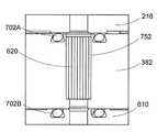
도 6은 본 발명의 실시예들에 따른, 다중 존 가스 주입 상부 전극 (501) 을 갖는 플라즈마 챔버 (600) 의 단면도이다. 플라즈마 챔버 (600) 의 단면도는 플라즈마 챔버의 상단 부분을 형성하는 다중-층 어셈블리를 예시한다. 다중 존 가스 주입 상부 전극 (501) 은 내측 전극 (201) 및 외측 전극 (310) 을 포함한다. 절연체 (250) 가 내측 전극 (201) 과 외측 전극 (310) 을 서로 분리시킨다. 절연체 (250) 는 석영 또는 몇몇 다른 적합한 절연성 재료일 수 있다. 내측 전극 (201) 및 외측 전극 (310) 은 인가된 서로 상이한 신호들을 가질 수 있다. 예시적으로, RF 신호가 내측 전극 (201) 에 인가되고 접지 또는 DC 전위가 외측 전극 (310) 에 인가될 수 있다.6 is a cross-sectional view of a
내측 전극 (201) 은 가스 분배 플레이트 (610) 상에 분리가능하게 장착된다. 가스 분배 플레이트 (610) 는 프로세스 가스 및 튜닝 가스를 상부 전극 (501) 에 걸쳐서 분배한다. 가스 분배 플레이트 (610) 는 프로세스 가스 및 튜닝 가스를 균일하게 분배하기 위해서 분배 배관들 (562, 564, 566) 및 채널들 (572, 574, 576) 을 포함한다.The
가스 분배 플레이트 (610) 는 절연체 플레이트 (612) 상에 장착된다. 절연체 플레이트 (612) 는 내측 전극 (201) 을 플라즈마 챔버 (600) 의 상단부를 형성하는 다른 층들로부터 전기적으로 절연시킨다. 가스 피드들 (552, 554, 556) 은 플라즈마 어레스터들 (arrestors) (620) 을 포함할 수 있다. 플라즈마 어레스터들 (arrestors) (620) 은 가스 피드들 (552, 554, 556) 내의 점화로부터 플라즈마를 방지한다.The
도 7a는 본 발명의 실시예들에 따른, 분배된 가스 공급 피드 (feed) (554, 556) 의 개략도이다. 분배된 가스 공급 피드 (feed) (554, 556) 중 하나 이상은 플라즈마 어레스터들 (arrestors) (620) 를 포함할 수 있다.7A is a schematic diagram of a dispensed
도 7b 내지 도 7f는 본 발명의 실시예들에 따른, 플라즈마 어레스터 (arrestor) (620,620') 의 개략도이다. 플라즈마 어레스터 (arrestor) (620,620') 는 분배된 가스 피드들 (554, 556) 내에서의 점화로부터 플라즈마를 실질적으로 방지한다. 시일들 (seals) (702A, 702B) 이 가스 누설을 방지한다.7B-7F are schematic diagrams of
플라즈마 어레스터 (arrestor) (620) 는 이 플라즈마 어레스터의 외측 부분을 따라서 다수의 소형 튜브들 (750) 및 세로홈형 채널 (fluted channels) (752) 을 포함할 수 있다. 이 다수의 소형 튜브들 (750) 및 세로홈형 채널 (fluted channels) (752) 은 플라즈마 어레스터 (arrestor) (620) 에 도달한 어떠한 플라즈마라도 소화시키도록 충분하게 작은 폭을 갖는다. 플라즈마 어레스터 (arrestor) (620) 는 또한 플라즈마 어레스터 (arrestor) (620) 에 도달한 어떠한 플라즈마라도 소화시키도록 지원할 수 있는 접지성 전극 (미도시) 을 포함할 수 있다.A
다른 플라즈마 어레스터 (arrestor) (620') 는 플라즈마 어레스터 (arrestor) (620') 에 도달한 어떠한 플라즈마라도 소화시키도록 충분하게 작은 폭을 갖는 나선형 채널 (spiral channel) 을 형성하는 나선형 외측 코일 (760) 을 갖는다. 나선형 외측 코일 (760) 은 플라즈마 어레스터 (arrestor) (620') 에 도달한 어떠한 플라즈마라도 소화시키도록 지원할 수 있도록 접지될 수 있다. 플라즈마 어레스터 (arrestor) (620,620') 는 세라믹 재료 (예를 들어서, 알루미나 또는 유사한 재료) 로 구성될 수 있다.The
도 8은 본 발명의 실시예들에 따른, 분포된 가스 존들 (502, 504, 506) 을 사용하여서 에지 에칭 레이트를 선택할 시에 수행되는 방법 동작들 (800) 을 예시하는 흐름도이다. 본 명세서에서 예시된 동작들은 예시적이며, 따라서 몇몇 동작들은 하위 동작들을 가질 수 있으며, 다른 실례에서는, 본 명세서에서 기술된 특정 동작들은 예시된 동작들에 포함되지 않을 수 있다. 이를 염두하고, 방법 및 동작들 (800) 이 이제 기술될 것이다.FIG. 8 is a flow chart illustrating
동작 (802) 에서, 플라즈마 (260) 가 플라즈마 챔버 (262) 내에서 생성된다. 동작 (804) 에서, 내측 가스 분배 존 1 (502) 에 걸친 에칭 레이트를 감소시킬지의 여부를 결정하는 질의가 행해진다. 내측 가스 분배 존 1 (502) 에 걸친 에칭 레이트가 감소될 것이면, 이 방법 동작들은 동작 (806) 에서 계속된다. 내측 가스 분배 존 1 (502) 에 걸친 에칭 레이트가 감소되지 않을 것이면, 이 방법 동작들은 동작 (808) 에서 계속된다.In
동작 (806) 에서, 튜닝 가스가 내측 가스 분배 존 1 (502) 내로 주입되고, 이 방법 동작들은 동작 (816) 에서 계속된다.At
동작 (808) 에서, 중간 가스 분배 존 2 (504) 에 걸친 에칭 레이트를 감소시킬지의 여부를 결정하는 질의가 행해진다. 중간 가스 분배 존 2 (504) 에 걸친 에칭 레이트가 감소될 것이면, 이 방법 동작들은 동작 (810) 에서 계속된다. 중간 가스 분배 존 2 (504) 에 걸친 에칭 레이트가 감소되지 않을 것이면, 이 방법 동작들은 동작 (812) 에서 계속된다.At
동작 (810) 에서, 튜닝 가스가 중간 가스 분배 존 2 (504) 내로 주입되고, 이 방법 동작들은 동작 (816) 에서 계속된다.In
동작 (812) 에서, 외측 가스 분배 존 3 (506) 에 걸친 에칭 레이트를 감소시킬지의 여부를 결정하는 질의가 행해진다. 외측 가스 분배 존 3 (506) 에 걸친 에칭 레이트가 감소될 것이면, 이 방법 동작들은 동작 (814) 에서 계속된다. 외측 가스 분배 존 3 (506) 에 걸친 에칭 레이트가 감소되지 않을 것이면, 이 방법 동작들은 동작 (816) 에서 계속된다.At
동작 (814) 에서, 튜닝 가스가 외측 가스 분배 존 3 (506) 내로 주입되고, 이 방법 동작들은 동작 (816) 에서 계속된다.In
동작 (816) 에서, 에칭 프로세싱을 완료할지의 여부를 결정하는 질의가 행해진다. 에칭 프로세스가 완료될 것이면, 이 방법 동작들은 종료될 수 있다. 에칭 프로세스가 완료되지 않을 것이면, 이 방법 동작들은 상술한 바와 같은 동작 (804) 에서 계속된다.At
도 9는 본 발명의 실시예들에 따른 컴퓨터 시스템 (900) 의 단순화된 개략도이다. 본 명세서에서 기술된 방법들은 통상적인 범용 컴퓨터 시스템과 같은 디지털 프로세싱 시스템을 사용하여서 수행될 수도 있음이 이해되어야 한다. 이와 달리, 오직 하나의 기능을 수행하도록 설계 또는 프로그래밍된 특정 목적의 컴퓨터들이 사용될 수도 있다. 컴퓨터 시스템은 버스 (910) 를 통해서 RAM (928), ROM (912) 및 대용량 저장 디바이스 (914) 로 접속되는 중앙 처리 유닛 (CPU) (904) 을 포함한다. 페이즈 제어 프로그램 (908) 은 RAM (928) 내에 상주하지만 또한 대용량 저장 디바이스 (914) 또는 ROM (912) 내에 상주할 수도 있다.9 is a simplified schematic diagram of a
대용량 저장 디바이스 (914) 는 로컬 또는 원격일 수 있는, 고정 디스크 드라이브 또는 플로피 디스크 드라이브와 같은 영구 데이터 저장 디바이스를 나타낸다. 네트워크 인터페이스 (930) 는 네트워크 (932) 를 통한 접속을 제공하여서, 다른 디바이스들과의 통신을 가능하게 한다. CPU (904) 는 범용 프로세서, 특정 목적의 프로세서 또는 특정하게 프로그래밍된 로직 디바이스로 구현될 수 있음이 이해되어야 한다. 입출력 (I/O) 인터페이스는 상이한 주변부들과의 통신을 제공하며 CPU (904), ROM (912), RAM (928) 및 대용량 저장 디바이스 (914) 에 버스 (910) 를 통해서 접속된다. 샘플 주변부들은 디스플레이 (918), 키보드 (922), 커서 제어부 (924), 이동식 매체 디바이스 (934) 등을 포함한다.
디스플레이 (918) 는 본 명세서에서 기술된 사용자 인터페이스들을 디스플레이하도록 구성된다. 키보드 (922), 커서 제어부 (924), 이동식 매체 디바이스 (934), 및 다른 주변부들은 명령 선택 시에 정보를 CPU (904) 로 전송하기 위해서 입출력 인터페이스 (920) 에 접속된다. 외부 디바이스들로의 데이터 및 이로부터의 데이터는 입출력 인터페이스 (920) 를 통해서 전송 및 수신될 수 있음이 이해되어야 한다. 또한, 실시예들은 유선 기반 또는 무선 네트워크를 통해서 링크된 원격 프로세싱 디바이스들에 의해서 태스크들이 수행되는 분산형 컴퓨팅 환경들에서 실시될 수도 있다.
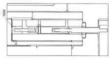
도 10a는 발명의 실시예들에 따른, 가열된 에지 링 (307) 의 개략도이다. 가열기 (205) 가 에지 링 (307) 을 가열하도록 선택적으로 포함될 수 있다.10A is a schematic view of a
도 10b 및 도 10c는 발명의 실시예들에 따른, 캠 록 (cam lock) (1010) 의 개략도들이다. 캠 록 (1010) 은 캠 록 샤프트 (1011) 및 캠 록 헤드 (1012) 를 포함한다. 캠 록 (1010) 은 정전 척 (140) 을 설비 플레이트 (1015) 에 고정하도록 래치 (1014) 와 결합된다.Figures 10B and 10C are schematic diagrams of a
도 10d 및 도 10e는 발명의 실시예들에 따른, 가열기들 (205) 로의 전기적 접속부들 (1020, 1022) 의 개략도들이다. 전기적 접속부들 (1020, 1022) 은 전력을 가열기들 (205) 에 접속시킨다. 캠 록들 (1010) 이 정전 척 (140) 을 설비 플레이트 (1015) 에 고정시킬 때에 전기적 접속부들 (1020, 1022) 은 가열기들 (205) 에 접속된다.10D and 10E are schematic diagrams of
도 10f는 발명의 실시예들에 따른, 광학적 온도 센서 (1030) 의 개략도이다. 광학적 온도 센서 (1030) 는 에지 링 (307) 의 온도를 모니터링하고 이 온도 데이터를 시스템 제어기에 전송한다.10F is a schematic diagram of an
위의 실시예들을 염두하면서, 본 발명은 컴퓨터 시스템들 내에 저장된 데이터를 수반하는 다양한 컴퓨터 구현형 동작들을 사용할 수 있다는 것이 이해되어야 한다. 이러한 동작들은 물리적 정량들의 물리적 조작을 요구하는 것들이다. 통상적으로, 반드시 그러한 것은 아니지만, 이러한 정량들은 저장, 전달, 조합, 비교 및 이와 달리 조작될 수 있는 전기적 신호 또는 자기적 신호의 형태를 취할 수 있다. 또한, 수행되는 조작들은 생성, 식별, 결정 또는 비교와 같은 용어들로 또한 지칭된다.With the above embodiments in mind, it should be understood that the present invention can employ a variety of computer-implemented operations involving data stored in computer systems. These operations are those requiring physical manipulation of physical quantities. Typically, though not necessarily, such quantities can take the form of electrical signals or magnetic signals that can be stored, transferred, combined, compared, and otherwise manipulated. In addition, the operations performed are also referred to as terms such as generation, identification, determination or comparison.
본 발명은 또한 컴퓨터 판독가능한 매체 상의 컴퓨터 판독가능한 코드 및/또는 로직으로서 실시될 수도 있다. 컴퓨터 판독가능한 매체는 이후에 컴퓨터 시스템에 의해서 판독될 수 있는 데이터를 저장할 수 있는 임의의 데이터 저장 디바이스이다. 컴퓨터 판독가능 매체의 실례들은 하드 드라이브, NAS (network attached storage), 로직 회로들, ROM, RAM, CD-ROM, CD-RW, 자기 테이프, 및 다른 광학 데이터 저장 디바이스 및 비광학 데이터 저장 디바이스를 포함한다. 컴퓨터 판독가능한 매체는 또한 컴퓨터 판독가능 코드가 배포되는 방식으로 저장 및 실행되도록 네트워크 접속된 컴퓨터 시스템들을 통해서 또한 배포될 수도 있다.The invention may also be embodied as computer readable code and / or logic on a computer readable medium. The computer-readable medium is any data storage device that is capable of storing data that can be thereafter read by a computer system. Examples of computer readable media include hard drives, network attached storage, logic circuits, ROM, RAM, CD-ROM, CD-RW, magnetic tape, and other optical and non-optical data storage devices do. The computer readable medium may also be distributed via networked computer systems so that the computer readable code is stored and executed in a manner in which the code is distributed.
위의 도면들에서 동작들에 의해서 표현된 인스트럭션들은 예시된 순서로 수행될 필요는 없으며 동작들에 의해서 표현되는 프로세싱 모두가 본 발명을 실시하는데 필요하지 않을 수 있다는 것이 또한 이해되어야 한다. 또한, 위의 도면들 중 임의의 도면에서 기술된 프로세스들은 또한 RAM, ROM 또는 하드 디스크 드라이브 중 임의의 것 또는 이들의 조합 내에 저장된 소프트웨어로 구현될 수도 있다.It should also be understood that the instructions represented by the operations in the above Figures need not be performed in the order shown and that not all of the processing represented by the operations may be necessary to practice the present invention. In addition, the processes described in any of the above figures may also be implemented in software stored in any of RAM, ROM, or hard disk drives, or a combination thereof.
전술한 발명은 이해의 명료성을 위해서 어느 정도 세부적으로 기술되었지만, 특정 변경 및 수정이 첨부된 청구범위 내에서 실시될 수 있음이 명백할 것이다. 따라서, 본 실시예들은 예시적이면서 비한정적으로 해석되어야 하며 본 발명은 본 명세서에서 주어진 세부사항들로 한정되지 않으며 첨부된 청구항의 범위 및 균등 범위 내에서 수정될 수 있다.Although the foregoing invention has been described in some detail for purposes of clarity of understanding, it will be apparent that certain changes and modifications may be practiced within the scope of the appended claims. Accordingly, the embodiments are to be construed as illustrative and not restrictive, and the invention is not to be limited to the details given herein, but may be modified within the scope and equivalence of the appended claims.
Claims (16)
Translated fromKorean플라즈마 챔버로서,
기판 지지부;
상기 기판 지지부에 대향하여 배치된 다중 존 가스 주입 상부 전극으로서, 상기 다중 존 가스 주입 상부 전극과 상기 기판 지지부 사이에 내측 플라즈마 영역이 규정되고, 상기 다중 존 가스 주입 상부 전극은 내측 전극, 상기 내측 전극을 둘러싸는 외측 전극, 및 상기 내측 전극과 상기 외측 전극을 분리하는 절연체를 포함하고, 상기 다중 존 가스 주입 상부 전극은 상기 절연체에 의해 둘러싸이고 가스 분배 플레이트 위에 배치된 절연체 플레이트를 포함하는 상기 가스 분배 플레이트를 포함하고, 상기 가스 분배 플레이트는 상기 절연체 플레이트와 상기 내측 전극 사이에 배치되고, 상기 다중 존 가스 주입 상부 전극은 내측 히터 및 외측 히터를 포함하고, 상기 내측 히터는 상기 절연체 플레이트, 상기 가스 분배 플레이트, 및 상기 내측 전극 위에 배치되고, 상기 외측 히터는 상기 외측 전극 위에 배치되고, 접지 전극이 상기 외측 히터와 상기 외측 전극 사이에 배치되고,
상기 다중 존 가스 주입 상부 전극은 복수의 동심 가스 주입 존들을 갖고, 상기 복수의 동심 가스 주입 존들 각각은 제 1 복수의 가스 유출 포트들 및 제 2 복수의 가스 유출 포트들을 포함하고, 상기 제 1 복수의 가스 유출 포트들은 제 1 가스 소스로 연결하도록 구성되고 그리고 상기 제 2 복수의 가스 유출 포트들은 제 2 가스 소스로 연결하도록 구성되는, 상기 다중 존 가스 주입 상부 전극; 및
상기 내측 플라즈마 영역을 둘러싸는 한정 구조체로서, 상기 한정 구조체는 상부 수평 벽의 하부 표면이 상기 다중 존 가스 주입 상부 전극의 상기 내측 전극의 하부 표면이 배치되는 레벨과 동일한 레벨로 배치되도록 상기 다중 존 가스 주입 상부 전극의 상기 외측 전극과 인터페이싱하는 상기 상부 수평 벽을 갖고, 상기 한정 구조체는 상기 기판 지지부와 인터페이싱하는 하부 수평 벽을 갖고, 상기 하부 수평 벽은 천공된 (perforated) 한정 링을 포함하고, 그리고 상기 한정 구조체는 상기 상부 수평 벽으로부터 상기 하부 수평 벽으로 연장하는 수직 벽을 갖고, 상기 상부 수평 벽의 상기 하부 표면, 상기 수직 벽의 내측 표면, 및 상기 하부 수평 벽의 상부 표면 각각은 외측 플라즈마 영역의 경계를 규정하고, 상기 외측 플라즈마 영역은 상기 내측 플라즈마 영역을 둘러싸는, 상기 한정 구조체를 포함하는, 상기 플라즈마 챔버; 및
상기 플라즈마 챔버에 연결된 제어기를 포함하는, 플라즈마 프로세싱 시스템.
In a plasma processing system,
As a plasma chamber,
A substrate support;
An inner plasma region is defined between the multi-zone gas injection top electrode and the substrate support, wherein the multi-zone gas injection top electrode defines an inner electrode, an inner electrode, And an insulator separating the inner electrode and the outer electrode, wherein the multizone gas injection top electrode comprises an insulator plate surrounded by the insulator and disposed on the gas distribution plate, Wherein the gas distribution plate is disposed between the insulator plate and the inner electrode, and wherein the multizone gas injection top electrode comprises an inner heater and an outer heater, the inner heater comprising: the insulator plate, the gas distribution Plate and the inner electrode The outer heater is disposed on the outer electrode, a ground electrode is disposed between said outer heater and the outer electrode, and
Wherein the multi-zone gas injection top electrode has a plurality of concentric gas injection zones, each of the plurality of concentric gas injection zones includes a first plurality of gas outlet ports and a second plurality of gas outlet ports, Wherein the gas outlet ports of the first gas inlet port are configured to connect to a first gas source and the second plurality of gas outlet ports are configured to connect to a second gas source; And
Wherein the confinement structure surrounds the inner plasma region such that the lower surface of the upper horizontal wall is disposed at the same level as the lower surface of the inner electrode of the multi- Wherein the confinement structure has a lower horizontal wall for interfacing with the substrate support, the lower horizontal wall comprising a perforated confinement ring, and Wherein the confinement structure has a vertical wall extending from the upper horizontal wall to the lower horizontal wall, each of the lower surface of the upper horizontal wall, the inner surface of the vertical wall, and the upper surface of the lower horizontal wall, And said outer plasma region defines a boundary of said inner plasma Surrounding the area, including the confinement structure, said plasma chamber; And
And a controller coupled to the plasma chamber.
상기 복수의 동심 가스 주입 존들 각각은 복수의 가스 피드들을 포함하고, 상기 복수의 가스 피드들은 대응하는 동심 가스 주입 존들에 걸쳐서 균일하게 분포되는, 플라즈마 프로세싱 시스템.
The method according to claim 1,
Wherein each of the plurality of concentric gas injection zones comprises a plurality of gas feeds and wherein the plurality of gas feeds are uniformly distributed over corresponding concentric gas injection zones.
제 1 동심 가스 주입 존들의 제 1 복수의 가스 피드들은 제 2 동심 가스 주입 존들의 제 2 복수의 가스 피드들과 정렬되는, 플라즈마 프로세싱 시스템.
3. The method of claim 2,
Wherein the first plurality of gas feeds of the first concentric gas injection zones are aligned with the second plurality of gas feeds of the second concentric gas injection zones.
제 1 동심 가스 주입 존들의 제 1 복수의 가스 피드들은 제 2 동심 가스 주입 존들의 제 2 복수의 가스 피드들로부터 시계방향으로 오프셋되는, 플라즈마 프로세싱 시스템.
3. The method of claim 2,
Wherein the first plurality of gas feeds of the first concentric gas injection zones are offset clockwise from the second plurality of gas feeds of the second concentric gas injection zones.
상기 복수의 가스 피드들 중 적어도 하나는 플라즈마 어레스터 (plasma arrestor) 를 포함하는, 플라즈마 프로세싱 시스템.
3. The method of claim 2,
Wherein at least one of the plurality of gas feeds comprises a plasma arrestor.
상기 플라즈마 어레스터는 상기 플라즈마 어레스터에 도달하는 어떠한 플라즈마라도 소화시키도록 충분한 폭을 갖는 복수의 소형 채널들을 포함하는, 플라즈마 프로세싱 시스템.
6. The method of claim 5,
Wherein the plasma arrestor comprises a plurality of small channels having a width sufficient to digest any plasma reaching the plasma arrestor.
상기 플라즈마 어레스터는 접지 전극을 포함하는, 플라즈마 프로세싱 시스템.
6. The method of claim 5,
Wherein the plasma arrestor comprises a ground electrode.
상기 다중 존 가스 주입 상부 전극에 연결된 RF 소스를 더 포함하는, 플라즈마 프로세싱 시스템.
The method according to claim 1,
Further comprising an RF source coupled to the multi-zone gas injection top electrode.
상기 하부 수평 벽은 상기 기판 지지부의 에지 링과 인터페이싱하는, 플라즈마 프로세싱 시스템.
The method according to claim 1,
Wherein the lower horizontal wall interfaces with an edge ring of the substrate support.
기판 지지부;
상기 기판 지지부 위에 배치된 다중 존 가스 주입 상부 전극 어셈블리로서, 상기 다중 존 가스 주입 상부 전극 어셈블리는 절연체 플레이트, 상기 절연체 플레이트 아래에 배치되고 상기 절연체 플레이트에 장착된 가스 분배 플레이트, 상기 가스 분배 플레이트 아래에 배치되고 상기 가스 분배 플레이트에 장착되고 RF (radio frequency) 신호를 수신하도록 구성된 내측 전극, 상기 내측 전극을 둘러싸지만 절연체를 통해 상기 내측 전극으로부터 분리되는 외측 전극, 상기 절연체 플레이트 위에 배치되고 상기 내측 전극에 열적으로 연결된 내측 히터, 상기 외측 전극 위에 배치되고 외측 히터와 상기 외측 전극 사이에 배치되는 접지 전극을 통해 상기 외측 전극에 열적으로 연결된 상기 외측 히터, 및 복수의 동심 가스 주입 존들을 포함하고, 상기 복수의 동심 가스 주입 존들 각각은 제 1 복수의 가스 유출 포트들 및 제 2 복수의 가스 유출 포트들을 포함하고, 상기 제 1 복수의 가스 유출 포트들은 제 1 가스 소스에 연결하도록 구성되고 상기 제 2 복수의 가스 유출 포트들은 제 2 가스 소스에 연결하도록 구성되는, 상기 다중 존 가스 주입 상부 전극 어셈블리; 및
상기 다중 존 가스 주입 상부 전극 어셈블리와 상기 기판 지지부 사이에 규정된 내측 플라즈마 영역을 둘러싸는 한정 구조체로서, 상기 한정 구조체는 상부 수평 벽의 하부 표면이 상기 다중 존 가스 주입 상부 전극의 상기 내측 전극의 하부 표면이 배치되는 레벨과 동일한 레벨로 배치되도록 상기 다중 존 가스 주입 상부 전극의 상기 외측 전극과 인터페이싱하는 상기 상부 수평 벽을 갖고, 상기 한정 구조체는 상기 기판 지지부와 인터페이싱하는 하부 수평 벽을 갖고, 상기 하부 수평 벽은 천공된 한정 링을 포함하고, 그리고 상기 한정 구조체는 상기 상부 수평 벽으로부터 상기 하부 수평 벽으로 연장하는 수직 벽을 갖고, 상기 상부 수평 벽의 상기 하부 표면, 상기 수직 벽의 내측 표면, 및 상기 하부 수평 벽의 상부 표면 각각은 외측 플라즈마 영역의 경계를 규정하고, 상기 외측 플라즈마 영역은 상기 내측 플라즈마 영역을 둘러싸는, 상기 한정 구조체를 포함하는, 플라즈마 챔버.
In the plasma chamber,
A substrate support;
A gas distribution plate disposed below the insulator plate and positioned below the gas distribution plate; a gas distribution plate disposed below the gas distribution plate; An inner electrode disposed and mounted on the gas distribution plate and configured to receive a radio frequency (RF) signal, an outer electrode surrounding the inner electrode but separated from the inner electrode via an insulator, And a plurality of concentric gas injection zones disposed on the outer electrode and thermally connected to the outer electrode through a ground electrode disposed between the outer heater and the outer electrode, Concentricity of Wherein each of the gas injection zones comprises a first plurality of gas outlet ports and a second plurality of gas outlet ports, wherein the first plurality of gas outlet ports are configured to connect to a first gas source and the second plurality of gas outlets The ports being configured to connect to a second gas source; And
A confinement structure surrounding an inner plasma region defined between the multi-zone gas-injected upper electrode assembly and the substrate support, wherein the confinement structure is configured such that a lower surface of the upper horizontal wall comprises a lower portion of the inner electrode Wherein the confinement structure has an upper horizontal wall that interfaces with the outer electrode of the multi-zone gas injection top electrode to be disposed at the same level as the level at which the surface is disposed, the confinement structure having a lower horizontal wall that interfaces with the substrate support, Wherein the horizontal wall comprises a perforated confinement ring and wherein the confinement structure has a vertical wall extending from the upper horizontal wall to the lower horizontal wall, the lower surface of the upper horizontal wall, the inner surface of the vertical wall, Each of the upper surfaces of the lower horizontal wall has an outer plasma region The outer plasma region defining a boundary, and the outer plasma region surrounding the inner plasma region.
상기 하부 수평 벽은 상기 기판 지지부의 에지 링과 인터페이싱하는, 플라즈마 챔버.
11. The method of claim 10,
And wherein the lower horizontal wall interfaces with an edge ring of the substrate support.
Applications Claiming Priority (5)
| Application Number | Priority Date | Filing Date | Title |
|---|---|---|---|
| US201161563510P | 2011-11-23 | 2011-11-23 | |
| US61/563,510 | 2011-11-23 | ||
| US13/438,473 | 2012-04-03 | ||
| US13/438,473US10622195B2 (en) | 2011-11-22 | 2012-04-03 | Multi zone gas injection upper electrode system |
| PCT/US2012/065684WO2013078098A1 (en) | 2011-11-23 | 2012-11-16 | Multi zone gas injection upper electrode system |
Publications (2)
| Publication Number | Publication Date |
|---|---|
| KR20140097436A KR20140097436A (en) | 2014-08-06 |
| KR101971312B1true KR101971312B1 (en) | 2019-04-22 |
Family
ID=48470218
Family Applications (1)
| Application Number | Title | Priority Date | Filing Date |
|---|---|---|---|
| KR1020147017227AActiveKR101971312B1 (en) | 2011-11-23 | 2012-11-16 | Multi zone gas injection upper electrode system |
Country Status (5)
| Country | Link |
|---|---|
| US (1) | US11594400B2 (en) |
| KR (1) | KR101971312B1 (en) |
| CN (1) | CN104024477B (en) |
| TW (1) | TWI661485B (en) |
| WO (1) | WO2013078098A1 (en) |
Families Citing this family (11)
| Publication number | Priority date | Publication date | Assignee | Title |
|---|---|---|---|---|
| US10077497B2 (en)* | 2014-05-30 | 2018-09-18 | Lam Research Corporation | Hollow cathode discharge (HCD) suppressing capacitively coupled plasma electrode and gas distribution faceplate |
| US10622217B2 (en)* | 2016-02-04 | 2020-04-14 | Samsung Electronics Co., Ltd. | Method of plasma etching and method of fabricating semiconductor device using the same |
| CN208835019U (en)* | 2018-11-12 | 2019-05-07 | 江苏鲁汶仪器有限公司 | Reaction chamber inner lining |
| WO2020100357A1 (en)* | 2019-08-05 | 2020-05-22 | 株式会社日立ハイテク | Plasma processing device |
| JP7308778B2 (en)* | 2020-02-26 | 2023-07-14 | 東京エレクトロン株式会社 | Plasma processing apparatus and plasma processing method |
| CN112750676B (en)* | 2020-11-24 | 2022-07-08 | 乐金显示光电科技(中国)有限公司 | Plasma processing device |
| CN114639585B (en)* | 2020-12-16 | 2025-02-14 | 中微半导体设备(上海)股份有限公司 | Confinement ring assembly, plasma processing device and exhaust control method thereof |
| JP2024521079A (en)* | 2021-05-24 | 2024-05-28 | ラム リサーチ コーポレーション | Multi-section plasma confinement ring structure |
| JP7724040B2 (en)* | 2022-02-24 | 2025-08-15 | 東京エレクトロン株式会社 | Substrate Processing Equipment |
| WO2024004148A1 (en)* | 2022-06-30 | 2024-01-04 | 日本碍子株式会社 | Member for semiconductor manufacturing device |
| AT528041A1 (en)* | 2024-02-21 | 2025-09-15 | Thermal Proc Solutions Gmbh | Device for the thermal treatment of a substance |
Citations (3)
| Publication number | Priority date | Publication date | Assignee | Title |
|---|---|---|---|---|
| US20010002582A1 (en) | 1999-07-08 | 2001-06-07 | Dunham Scott William | Method and apparatus for providing uniform gas delivery to substrates in CVD and PECVD processes |
| US20030136766A1 (en) | 2000-03-17 | 2003-07-24 | Applied Materials, Inc. | MERIE plasma reactor with overhead RF electrode tuned to the plasma with arcing suppression |
| US20070251642A1 (en) | 2006-04-28 | 2007-11-01 | Applied Materials, Inc. | Plasma reactor apparatus with multiple gas injection zones having time-changing separate configurable gas compositions for each zone |
Family Cites Families (132)
| Publication number | Priority date | Publication date | Assignee | Title |
|---|---|---|---|---|
| EP1120817B8 (en)* | 1991-03-26 | 2007-10-10 | Ngk Insulators, Ltd. | Use of a corrosion-resistant member |
| US6518195B1 (en)* | 1991-06-27 | 2003-02-11 | Applied Materials, Inc. | Plasma reactor using inductive RF coupling, and processes |
| US6063233A (en)* | 1991-06-27 | 2000-05-16 | Applied Materials, Inc. | Thermal control apparatus for inductively coupled RF plasma reactor having an overhead solenoidal antenna |
| JPH0521393A (en)* | 1991-07-11 | 1993-01-29 | Sony Corp | Plasma processor |
| US5822171A (en)* | 1994-02-22 | 1998-10-13 | Applied Materials, Inc. | Electrostatic chuck with improved erosion resistance |
| US5900103A (en)* | 1994-04-20 | 1999-05-04 | Tokyo Electron Limited | Plasma treatment method and apparatus |
| US5620524A (en)* | 1995-02-27 | 1997-04-15 | Fan; Chiko | Apparatus for fluid delivery in chemical vapor deposition systems |
| US6902683B1 (en)* | 1996-03-01 | 2005-06-07 | Hitachi, Ltd. | Plasma processing apparatus and plasma processing method |
| US6036878A (en)* | 1996-02-02 | 2000-03-14 | Applied Materials, Inc. | Low density high frequency process for a parallel-plate electrode plasma reactor having an inductive antenna |
| US5846883A (en)* | 1996-07-10 | 1998-12-08 | Cvc, Inc. | Method for multi-zone high-density inductively-coupled plasma generation |
| US5968587A (en)* | 1996-11-13 | 1999-10-19 | Applied Materials, Inc. | Systems and methods for controlling the temperature of a vapor deposition apparatus |
| US5844195A (en)* | 1996-11-18 | 1998-12-01 | Applied Materials, Inc. | Remote plasma source |
| US6841203B2 (en)* | 1997-12-24 | 2005-01-11 | Tokyo Electron Limited | Method of forming titanium film by CVD |
| US6302964B1 (en)* | 1998-06-16 | 2001-10-16 | Applied Materials, Inc. | One-piece dual gas faceplate for a showerhead in a semiconductor wafer processing system |
| KR100331544B1 (en)* | 1999-01-18 | 2002-04-06 | 윤종용 | Method for introducing gases into a reactor chamber and a shower head used therein |
| US6528751B1 (en)* | 2000-03-17 | 2003-03-04 | Applied Materials, Inc. | Plasma reactor with overhead RF electrode tuned to the plasma |
| US7220937B2 (en)* | 2000-03-17 | 2007-05-22 | Applied Materials, Inc. | Plasma reactor with overhead RF source power electrode with low loss, low arcing tendency and low contamination |
| US6494958B1 (en)* | 2000-06-29 | 2002-12-17 | Applied Materials Inc. | Plasma chamber support with coupled electrode |
| AU2001279189A1 (en)* | 2000-08-08 | 2002-02-18 | Tokyo Electron Limited | Plasma processing method and apparatus |
| US6302965B1 (en)* | 2000-08-15 | 2001-10-16 | Applied Materials, Inc. | Dispersion plate for flowing vaporizes compounds used in chemical vapor deposition of films onto semiconductor surfaces |
| US20020197402A1 (en)* | 2000-12-06 | 2002-12-26 | Chiang Tony P. | System for depositing a film by modulated ion-induced atomic layer deposition (MII-ALD) |
| JP3924483B2 (en)* | 2001-03-19 | 2007-06-06 | アイピーエス リミテッド | Chemical vapor deposition equipment |
| US6974523B2 (en)* | 2001-05-16 | 2005-12-13 | Lam Research Corporation | Hollow anode plasma reactor and method |
| US20030027428A1 (en)* | 2001-07-18 | 2003-02-06 | Applied Materials, Inc. | Bypass set up for integration of remote optical endpoint for CVD chamber |
| US6984288B2 (en)* | 2001-08-08 | 2006-01-10 | Lam Research Corporation | Plasma processor in plasma confinement region within a vacuum chamber |
| US20030045098A1 (en)* | 2001-08-31 | 2003-03-06 | Applied Materials, Inc. | Method and apparatus for processing a wafer |
| US6855906B2 (en)* | 2001-10-16 | 2005-02-15 | Adam Alexander Brailove | Induction plasma reactor |
| US6590344B2 (en)* | 2001-11-20 | 2003-07-08 | Taiwan Semiconductor Manufacturing Co., Ltd. | Selectively controllable gas feed zones for a plasma reactor |
| KR100450068B1 (en)* | 2001-11-23 | 2004-09-24 | 주성엔지니어링(주) | Multi-sectored flat board type showerhead used in CVD apparatus |
| WO2003073489A1 (en)* | 2002-02-28 | 2003-09-04 | Tokyo Electron Limited | Plasma processing device and feeding unit |
| US6646233B2 (en)* | 2002-03-05 | 2003-11-11 | Hitachi High-Technologies Corporation | Wafer stage for wafer processing apparatus and wafer processing method |
| FR2838020B1 (en)* | 2002-03-28 | 2004-07-02 | Centre Nat Rech Scient | PLASMA CONTAINMENT DEVICE |
| US20030188685A1 (en)* | 2002-04-08 | 2003-10-09 | Applied Materials, Inc. | Laser drilled surfaces for substrate processing chambers |
| US7013834B2 (en)* | 2002-04-19 | 2006-03-21 | Nordson Corporation | Plasma treatment system |
| JP2006507662A (en)* | 2002-06-28 | 2006-03-02 | 東京エレクトロン株式会社 | Arc suppression method and system in plasma processing system |
| US6821347B2 (en)* | 2002-07-08 | 2004-11-23 | Micron Technology, Inc. | Apparatus and method for depositing materials onto microelectronic workpieces |
| TWI283899B (en)* | 2002-07-09 | 2007-07-11 | Applied Materials Inc | Capacitively coupled plasma reactor with magnetic plasma control |
| US20040027781A1 (en)* | 2002-08-12 | 2004-02-12 | Hiroji Hanawa | Low loss RF bias electrode for a plasma reactor with enhanced wafer edge RF coupling and highly efficient wafer cooling |
| US6887521B2 (en)* | 2002-08-15 | 2005-05-03 | Micron Technology, Inc. | Gas delivery system for pulsed-type deposition processes used in the manufacturing of micro-devices |
| US20040040503A1 (en)* | 2002-08-29 | 2004-03-04 | Micron Technology, Inc. | Micromachines for delivering precursors and gases for film deposition |
| US20040040502A1 (en)* | 2002-08-29 | 2004-03-04 | Micron Technology, Inc. | Micromachines for delivering precursors and gases for film deposition |
| US7163602B2 (en)* | 2003-03-07 | 2007-01-16 | Ogle John S | Apparatus for generating planar plasma using concentric coils and ferromagnetic cores |
| US7335396B2 (en)* | 2003-04-24 | 2008-02-26 | Micron Technology, Inc. | Methods for controlling mass flow rates and pressures in passageways coupled to reaction chambers and systems for depositing material onto microfeature workpieces in reaction chambers |
| US8409400B2 (en)* | 2003-05-07 | 2013-04-02 | Gen Co., Ltd. | Inductive plasma chamber having multi discharge tube bridge |
| US7455748B2 (en)* | 2003-06-20 | 2008-11-25 | Lam Research Corporation | Magnetic enhancement for mechanical confinement of plasma |
| US7144521B2 (en)* | 2003-08-22 | 2006-12-05 | Lam Research Corporation | High aspect ratio etch using modulation of RF powers of various frequencies |
| JP4607517B2 (en)* | 2003-09-03 | 2011-01-05 | 東京エレクトロン株式会社 | Plasma processing equipment |
| US7581511B2 (en)* | 2003-10-10 | 2009-09-01 | Micron Technology, Inc. | Apparatus and methods for manufacturing microfeatures on workpieces using plasma vapor processes |
| US7464662B2 (en)* | 2004-01-28 | 2008-12-16 | Tokyo Electron Limited | Compact, distributed inductive element for large scale inductively-coupled plasma sources |
| US8317968B2 (en)* | 2004-04-30 | 2012-11-27 | Lam Research Corporation | Apparatus including gas distribution member supplying process gas and radio frequency (RF) power for plasma processing |
| US7169256B2 (en)* | 2004-05-28 | 2007-01-30 | Lam Research Corporation | Plasma processor with electrode responsive to multiple RF frequencies |
| US7699932B2 (en)* | 2004-06-02 | 2010-04-20 | Micron Technology, Inc. | Reactors, systems and methods for depositing thin films onto microfeature workpieces |
| WO2006004045A1 (en)* | 2004-07-05 | 2006-01-12 | Tokyo Electron Limited | Treating device and heater unit |
| US7534301B2 (en)* | 2004-09-21 | 2009-05-19 | Applied Materials, Inc. | RF grounding of cathode in process chamber |
| US7323116B2 (en)* | 2004-09-27 | 2008-01-29 | Lam Research Corporation | Methods and apparatus for monitoring a process in a plasma processing system by measuring self-bias voltage |
| US7393432B2 (en)* | 2004-09-29 | 2008-07-01 | Lam Research Corporation | RF ground switch for plasma processing system |
| US7244311B2 (en)* | 2004-10-13 | 2007-07-17 | Lam Research Corporation | Heat transfer system for improved semiconductor processing uniformity |
| US7632375B2 (en)* | 2004-12-30 | 2009-12-15 | Lam Research Corporation | Electrically enhancing the confinement of plasma |
| US20060237138A1 (en)* | 2005-04-26 | 2006-10-26 | Micron Technology, Inc. | Apparatuses and methods for supporting microelectronic devices during plasma-based fabrication processes |
| US7641762B2 (en)* | 2005-09-02 | 2010-01-05 | Applied Materials, Inc. | Gas sealing skirt for suspended showerhead in process chamber |
| US8092638B2 (en)* | 2005-10-11 | 2012-01-10 | Applied Materials Inc. | Capacitively coupled plasma reactor having a cooled/heated wafer support with uniform temperature distribution |
| US7397232B2 (en)* | 2005-10-21 | 2008-07-08 | The University Of Akron | Coulter counter having a plurality of channels |
| US8674255B1 (en)* | 2005-12-08 | 2014-03-18 | Lam Research Corporation | Apparatus and method for controlling etch uniformity |
| US7683289B2 (en)* | 2005-12-16 | 2010-03-23 | Lam Research Corporation | Apparatus and method for controlling plasma density profile |
| US7619179B2 (en)* | 2006-01-20 | 2009-11-17 | Tokyo Electron Limited | Electrode for generating plasma and plasma processing apparatus using same |
| US20070170155A1 (en)* | 2006-01-20 | 2007-07-26 | Fink Steven T | Method and apparatus for modifying an etch profile |
| US8012306B2 (en)* | 2006-02-15 | 2011-09-06 | Lam Research Corporation | Plasma processing reactor with multiple capacitive and inductive power sources |
| US8097120B2 (en)* | 2006-02-21 | 2012-01-17 | Lam Research Corporation | Process tuning gas injection from the substrate edge |
| US8911590B2 (en)* | 2006-02-27 | 2014-12-16 | Lam Research Corporation | Integrated capacitive and inductive power sources for a plasma etching chamber |
| US7943523B2 (en)* | 2006-02-28 | 2011-05-17 | Tokyo Electron Limited | Plasma etching method and computer readable storage medium |
| US7432467B2 (en)* | 2006-03-28 | 2008-10-07 | Tokyo Electron Limited | Plasma processing apparatus |
| US8138445B2 (en)* | 2006-03-30 | 2012-03-20 | Tokyo Electron Limited | Plasma processing apparatus and plasma processing method |
| US7541292B2 (en)* | 2006-04-28 | 2009-06-02 | Applied Materials, Inc. | Plasma etch process with separately fed carbon-lean and carbon-rich polymerizing etch gases in independent inner and outer gas injection zones |
| US20080006205A1 (en)* | 2006-07-10 | 2008-01-10 | Douglas Keil | Apparatus and Method for Controlling Plasma Potential |
| US7837826B2 (en)* | 2006-07-18 | 2010-11-23 | Lam Research Corporation | Hybrid RF capacitively and inductively coupled plasma source using multifrequency RF powers and methods of use thereof |
| JP4801522B2 (en)* | 2006-07-21 | 2011-10-26 | 株式会社日立ハイテクノロジーズ | Semiconductor manufacturing apparatus and plasma processing method |
| US20080035306A1 (en)* | 2006-08-08 | 2008-02-14 | White John M | Heating and cooling of substrate support |
| US7829815B2 (en)* | 2006-09-22 | 2010-11-09 | Taiwan Semiconductor Manufacturing Co., Ltd. | Adjustable electrodes and coils for plasma density distribution control |
| DE102006048816A1 (en)* | 2006-10-16 | 2008-04-17 | Iplas Innovative Plasma Systems Gmbh | Apparatus and method for local generation of microwave plasmas |
| US7776178B2 (en)* | 2006-10-25 | 2010-08-17 | Applied Materials, Inc. | Suspension for showerhead in process chamber |
| WO2008089168A2 (en)* | 2007-01-19 | 2008-07-24 | Applied Materials, Inc. | Plasma immersion chamber |
| US7879731B2 (en)* | 2007-01-30 | 2011-02-01 | Applied Materials, Inc. | Improving plasma process uniformity across a wafer by apportioning power among plural VHF sources |
| US20080179289A1 (en)* | 2007-01-30 | 2008-07-31 | Collins Kenneth S | Process for wafer backside polymer removal with a plasma stream |
| US7972470B2 (en)* | 2007-05-03 | 2011-07-05 | Applied Materials, Inc. | Asymmetric grounding of rectangular susceptor |
| WO2008154222A1 (en)* | 2007-06-06 | 2008-12-18 | Mks Instruments, Inc. | Particle reduction through gas and plasma source control |
| US20090025879A1 (en)* | 2007-07-26 | 2009-01-29 | Shahid Rauf | Plasma reactor with reduced electrical skew using a conductive baffle |
| JP5514413B2 (en)* | 2007-08-17 | 2014-06-04 | 東京エレクトロン株式会社 | Plasma etching method |
| JP5194125B2 (en)* | 2007-09-25 | 2013-05-08 | ラム リサーチ コーポレーション | Temperature control module for showerhead electrode assembly, showerhead electrode assembly and method for controlling temperature of upper electrode of showerhead electrode assembly |
| SG187386A1 (en)* | 2007-12-19 | 2013-02-28 | Lam Res Corp | A composite showerhead electrode assembly for a plasma processing apparatus |
| SG188141A1 (en)* | 2008-02-08 | 2013-03-28 | Lam Res Corp | A protective coating for a plasma processing chamber part and a method of use |
| US7558045B1 (en)* | 2008-03-20 | 2009-07-07 | Novellus Systems, Inc. | Electrostatic chuck assembly with capacitive sense feature, and related operating method |
| JP5213496B2 (en)* | 2008-03-31 | 2013-06-19 | 東京エレクトロン株式会社 | Plasma etching method and computer-readable storage medium |
| US8263499B2 (en)* | 2008-03-31 | 2012-09-11 | Tokyo Electron Limited | Plasma processing method and computer readable storage medium |
| US20090275206A1 (en)* | 2008-05-05 | 2009-11-05 | Applied Materials, Inc. | Plasma process employing multiple zone gas distribution for improved uniformity of critical dimension bias |
| US8679288B2 (en)* | 2008-06-09 | 2014-03-25 | Lam Research Corporation | Showerhead electrode assemblies for plasma processing apparatuses |
| US8206552B2 (en)* | 2008-06-25 | 2012-06-26 | Applied Materials, Inc. | RF power delivery system in a semiconductor apparatus |
| CN102084474B (en)* | 2008-07-07 | 2012-11-14 | 朗姆研究公司 | Capacitively Coupled Electrostatic (CCE) Probe Device and Method for Detecting Unclamping in a Plasma Processing Chamber |
| KR20100031960A (en)* | 2008-09-17 | 2010-03-25 | 삼성전자주식회사 | Plasma generating apparatus |
| JP5295833B2 (en)* | 2008-09-24 | 2013-09-18 | 株式会社東芝 | Substrate processing apparatus and substrate processing method |
| US8070925B2 (en)* | 2008-10-17 | 2011-12-06 | Applied Materials, Inc. | Physical vapor deposition reactor with circularly symmetric RF feed and DC feed to the sputter target |
| US20100098875A1 (en)* | 2008-10-17 | 2010-04-22 | Andreas Fischer | Pre-coating and wafer-less auto-cleaning system and method |
| US20100116788A1 (en)* | 2008-11-12 | 2010-05-13 | Lam Research Corporation | Substrate temperature control by using liquid controlled multizone substrate support |
| US8099995B2 (en)* | 2008-12-16 | 2012-01-24 | Agilent Technologies, Inc. | Choked flow isolator for noise reduction in analytical systems |
| JP5203986B2 (en)* | 2009-01-19 | 2013-06-05 | 東京エレクトロン株式会社 | Focus ring heating method, plasma etching method, plasma etching apparatus and computer storage medium |
| TWI558843B (en)* | 2009-02-04 | 2016-11-21 | 應用材料股份有限公司 | Ground return for plasma processes |
| US8503151B2 (en)* | 2009-09-30 | 2013-08-06 | Lam Research Corporation | Plasma arrestor insert |
| US8485128B2 (en)* | 2010-06-30 | 2013-07-16 | Lam Research Corporation | Movable ground ring for a plasma processing chamber |
| US9184028B2 (en)* | 2010-08-04 | 2015-11-10 | Lam Research Corporation | Dual plasma volume processing apparatus for neutral/ion flux control |
| US20130059448A1 (en)* | 2011-09-07 | 2013-03-07 | Lam Research Corporation | Pulsed Plasma Chamber in Dual Chamber Configuration |
| US9117767B2 (en)* | 2011-07-21 | 2015-08-25 | Lam Research Corporation | Negative ion control for dielectric etch |
| US8573152B2 (en)* | 2010-09-03 | 2013-11-05 | Lam Research Corporation | Showerhead electrode |
| US20120086541A1 (en)* | 2010-10-08 | 2012-04-12 | Cooper Technologies Company | Solid-core surge arrester |
| US9177756B2 (en)* | 2011-04-11 | 2015-11-03 | Lam Research Corporation | E-beam enhanced decoupled source for semiconductor processing |
| US8618446B2 (en)* | 2011-06-30 | 2013-12-31 | Applied Materials, Inc. | Substrate support with substrate heater and symmetric RF return |
| US9039911B2 (en)* | 2012-08-27 | 2015-05-26 | Lam Research Corporation | Plasma-enhanced etching in an augmented plasma processing system |
| US20130122711A1 (en)* | 2011-11-10 | 2013-05-16 | Alexei Marakhtanov | System, method and apparatus for plasma sheath voltage control |
| US8652298B2 (en)* | 2011-11-21 | 2014-02-18 | Lam Research Corporation | Triode reactor design with multiple radiofrequency powers |
| US9263240B2 (en)* | 2011-11-22 | 2016-02-16 | Lam Research Corporation | Dual zone temperature control of upper electrodes |
| US8898889B2 (en)* | 2011-11-22 | 2014-12-02 | Lam Research Corporation | Chuck assembly for plasma processing |
| WO2013078434A1 (en)* | 2011-11-24 | 2013-05-30 | Lam Research Corporation | Plasma processing chamber with flexible symmetric rf return strap |
| US8932429B2 (en)* | 2012-02-23 | 2015-01-13 | Lam Research Corporation | Electronic knob for tuning radial etch non-uniformity at VHF frequencies |
| US9881772B2 (en)* | 2012-03-28 | 2018-01-30 | Lam Research Corporation | Multi-radiofrequency impedance control for plasma uniformity tuning |
| JP5794194B2 (en)* | 2012-04-19 | 2015-10-14 | 東京エレクトロン株式会社 | Substrate processing equipment |
| US9018022B2 (en)* | 2012-09-24 | 2015-04-28 | Lam Research Corporation | Showerhead electrode assembly in a capacitively coupled plasma processing apparatus |
| US10177014B2 (en)* | 2012-12-14 | 2019-01-08 | Applied Materials, Inc. | Thermal radiation barrier for substrate processing chamber components |
| US9997381B2 (en)* | 2013-02-18 | 2018-06-12 | Lam Research Corporation | Hybrid edge ring for plasma wafer processing |
| JP5971870B2 (en)* | 2013-11-29 | 2016-08-17 | 株式会社日立国際電気 | Substrate processing apparatus, semiconductor device manufacturing method, and recording medium |
| US10781518B2 (en)* | 2014-12-11 | 2020-09-22 | Applied Materials, Inc. | Gas cooled electrostatic chuck (ESC) having a gas channel formed therein and coupled to a gas box on both ends of the gas channel |
| KR102747645B1 (en)* | 2019-10-10 | 2024-12-27 | 삼성전자주식회사 | Electro-static chuck and substrate processing apparatus including the same |
| JP7330115B2 (en)* | 2020-02-07 | 2023-08-21 | 東京エレクトロン株式会社 | Plasma processing apparatus and plasma processing method |
| JP7458195B2 (en)* | 2020-02-10 | 2024-03-29 | 東京エレクトロン株式会社 | Mounting table, plasma processing device, and cleaning processing method |
| US20210249232A1 (en)* | 2020-02-10 | 2021-08-12 | Taiwan Semiconductor Manufacturing Company Ltd. | Apparatus and method for etching |
- 2012
- 2012-11-16KRKR1020147017227Apatent/KR101971312B1/enactiveActive
- 2012-11-16WOPCT/US2012/065684patent/WO2013078098A1/enactiveApplication Filing
- 2012-11-16CNCN201280057644.3Apatent/CN104024477B/enactiveActive
- 2012-11-23TWTW101144011Apatent/TWI661485B/enactive
- 2020
- 2020-04-10USUS16/845,723patent/US11594400B2/enactiveActive
Patent Citations (3)
| Publication number | Priority date | Publication date | Assignee | Title |
|---|---|---|---|---|
| US20010002582A1 (en) | 1999-07-08 | 2001-06-07 | Dunham Scott William | Method and apparatus for providing uniform gas delivery to substrates in CVD and PECVD processes |
| US20030136766A1 (en) | 2000-03-17 | 2003-07-24 | Applied Materials, Inc. | MERIE plasma reactor with overhead RF electrode tuned to the plasma with arcing suppression |
| US20070251642A1 (en) | 2006-04-28 | 2007-11-01 | Applied Materials, Inc. | Plasma reactor apparatus with multiple gas injection zones having time-changing separate configurable gas compositions for each zone |
Also Published As
| Publication number | Publication date |
|---|---|
| CN104024477A (en) | 2014-09-03 |
| TWI661485B (en) | 2019-06-01 |
| TW201335993A (en) | 2013-09-01 |
| CN104024477B (en) | 2016-05-18 |
| US20200243307A1 (en) | 2020-07-30 |
| KR20140097436A (en) | 2014-08-06 |
| US11594400B2 (en) | 2023-02-28 |
| WO2013078098A1 (en) | 2013-05-30 |
Similar Documents
| Publication | Publication Date | Title |
|---|---|---|
| US11594400B2 (en) | Multi zone gas injection upper electrode system | |
| US10622195B2 (en) | Multi zone gas injection upper electrode system | |
| KR102594442B1 (en) | Plasma processing apparatus | |
| KR102468738B1 (en) | Multi-electrode substrate support assembly and phase control system | |
| US8097120B2 (en) | Process tuning gas injection from the substrate edge | |
| KR102302723B1 (en) | Tunable temperature controlled substrate support assembly | |
| US10403534B2 (en) | Pixilated cooling, temperature controlled substrate support assembly | |
| US6359250B1 (en) | RF matching network with distributed outputs | |
| US20160079039A1 (en) | Dual Plasma Volume Processing Apparatus for Neutral/Ion Flux Control | |
| US20160148813A1 (en) | Gas injection method for uniformly processing a semiconductor substrate in a semiconductor substrate processing apparatus | |
| KR20170127358A (en) | Adjustable side gas plenum for edge etch rate control in a downstream reactor | |
| CN103890928A (en) | Electrostatic chuck | |
| KR20210032904A (en) | Method of etching silicon oxide film and plasma processing apparatus | |
| US20210375586A1 (en) | An advanced ceramic lid with embedded heater elements and embedded rf coil for hdp cvd and inductively coupled plasma treatment chambers | |
| US12016092B2 (en) | Gas distribution ceramic heater for deposition chamber | |
| KR102031393B1 (en) | Dual zone temperature control of upper electrodes | |
| KR20210018145A (en) | Placing table and substrate processing apparatus | |
| KR102870617B1 (en) | Push-pull power supply for multi-mesh processing chambers | |
| TW202307910A (en) | Electrode for plasma processing apparatus and plasma processing apparatus | |
| US20140102641A1 (en) | Field enhanced inductively coupled plasma processing apparatus and plasma forming method | |
| TW202301909A (en) | Temperature control method and temperature control device |
Legal Events
| Date | Code | Title | Description |
|---|---|---|---|
| PA0105 | International application | Patent event date:20140623 Patent event code:PA01051R01D Comment text:International Patent Application | |
| PG1501 | Laying open of application | ||
| A201 | Request for examination | ||
| PA0201 | Request for examination | Patent event code:PA02012R01D Patent event date:20171109 Comment text:Request for Examination of Application | |
| E902 | Notification of reason for refusal | ||
| PE0902 | Notice of grounds for rejection | Comment text:Notification of reason for refusal Patent event date:20181022 Patent event code:PE09021S01D | |
| E701 | Decision to grant or registration of patent right | ||
| PE0701 | Decision of registration | Patent event code:PE07011S01D Comment text:Decision to Grant Registration Patent event date:20190122 | |
| GRNT | Written decision to grant | ||
| PR0701 | Registration of establishment | Comment text:Registration of Establishment Patent event date:20190416 Patent event code:PR07011E01D | |
| PR1002 | Payment of registration fee | Payment date:20190416 End annual number:3 Start annual number:1 | |
| PG1601 | Publication of registration | ||
| PR1001 | Payment of annual fee | Payment date:20220404 Start annual number:4 End annual number:4 | |
| PR1001 | Payment of annual fee | Payment date:20230404 Start annual number:5 End annual number:5 |