KR101971287B1 - Led driver apparatus - Google Patents
Led driver apparatusDownload PDFInfo
- Publication number
- KR101971287B1 KR101971287B1KR1020110087461AKR20110087461AKR101971287B1KR 101971287 B1KR101971287 B1KR 101971287B1KR 1020110087461 AKR1020110087461 AKR 1020110087461AKR 20110087461 AKR20110087461 AKR 20110087461AKR 101971287 B1KR101971287 B1KR 101971287B1
- Authority
- KR
- South Korea
- Prior art keywords
- dimming signal
- led array
- voltage
- signal
- forward voltage
- Prior art date
- Legal status (The legal status is an assumption and is not a legal conclusion. Google has not performed a legal analysis and makes no representation as to the accuracy of the status listed.)
- Active
Links
- 230000006866deteriorationEffects0.000claimsabstractdescription15
- 238000000034methodMethods0.000claimsdescription11
- 230000001934delayEffects0.000claimsdescription4
- 230000003111delayed effectEffects0.000claimsdescription4
- 238000010586diagramMethods0.000description11
- 230000002159abnormal effectEffects0.000description4
- 239000004973liquid crystal related substanceSubstances0.000description4
- 230000010363phase shiftEffects0.000description3
- 238000003491arrayMethods0.000description2
- 238000003912environmental pollutionMethods0.000description1
- QSHDDOUJBYECFT-UHFFFAOYSA-NmercuryChemical compound[Hg]QSHDDOUJBYECFT-UHFFFAOYSA-N0.000description1
- 229910052753mercuryInorganic materials0.000description1
- 230000000630rising effectEffects0.000description1
- 238000004904shorteningMethods0.000description1
- 239000000126substanceSubstances0.000description1
Images


Classifications
- H—ELECTRICITY
- H05—ELECTRIC TECHNIQUES NOT OTHERWISE PROVIDED FOR
- H05B—ELECTRIC HEATING; ELECTRIC LIGHT SOURCES NOT OTHERWISE PROVIDED FOR; CIRCUIT ARRANGEMENTS FOR ELECTRIC LIGHT SOURCES, IN GENERAL
- H05B47/00—Circuit arrangements for operating light sources in general, i.e. where the type of light source is not relevant
- H05B47/10—Controlling the light source
- H05B47/165—Controlling the light source following a pre-assigned programmed sequence; Logic control [LC]
- G—PHYSICS
- G09—EDUCATION; CRYPTOGRAPHY; DISPLAY; ADVERTISING; SEALS
- G09G—ARRANGEMENTS OR CIRCUITS FOR CONTROL OF INDICATING DEVICES USING STATIC MEANS TO PRESENT VARIABLE INFORMATION
- G09G3/00—Control arrangements or circuits, of interest only in connection with visual indicators other than cathode-ray tubes
- G09G3/20—Control arrangements or circuits, of interest only in connection with visual indicators other than cathode-ray tubes for presentation of an assembly of a number of characters, e.g. a page, by composing the assembly by combination of individual elements arranged in a matrix no fixed position being assigned to or needed to be assigned to the individual characters or partial characters
- G09G3/34—Control arrangements or circuits, of interest only in connection with visual indicators other than cathode-ray tubes for presentation of an assembly of a number of characters, e.g. a page, by composing the assembly by combination of individual elements arranged in a matrix no fixed position being assigned to or needed to be assigned to the individual characters or partial characters by control of light from an independent source
- G09G3/36—Control arrangements or circuits, of interest only in connection with visual indicators other than cathode-ray tubes for presentation of an assembly of a number of characters, e.g. a page, by composing the assembly by combination of individual elements arranged in a matrix no fixed position being assigned to or needed to be assigned to the individual characters or partial characters by control of light from an independent source using liquid crystals
- G—PHYSICS
- G09—EDUCATION; CRYPTOGRAPHY; DISPLAY; ADVERTISING; SEALS
- G09G—ARRANGEMENTS OR CIRCUITS FOR CONTROL OF INDICATING DEVICES USING STATIC MEANS TO PRESENT VARIABLE INFORMATION
- G09G5/00—Control arrangements or circuits for visual indicators common to cathode-ray tube indicators and other visual indicators
- G09G5/10—Intensity circuits
- H—ELECTRICITY
- H05—ELECTRIC TECHNIQUES NOT OTHERWISE PROVIDED FOR
- H05B—ELECTRIC HEATING; ELECTRIC LIGHT SOURCES NOT OTHERWISE PROVIDED FOR; CIRCUIT ARRANGEMENTS FOR ELECTRIC LIGHT SOURCES, IN GENERAL
- H05B45/00—Circuit arrangements for operating light-emitting diodes [LED]
- H05B45/30—Driver circuits
- H05B45/32—Pulse-control circuits
- H05B45/325—Pulse-width modulation [PWM]
- H—ELECTRICITY
- H05—ELECTRIC TECHNIQUES NOT OTHERWISE PROVIDED FOR
- H05B—ELECTRIC HEATING; ELECTRIC LIGHT SOURCES NOT OTHERWISE PROVIDED FOR; CIRCUIT ARRANGEMENTS FOR ELECTRIC LIGHT SOURCES, IN GENERAL
- H05B45/00—Circuit arrangements for operating light-emitting diodes [LED]
- H05B45/30—Driver circuits
- H05B45/37—Converter circuits
- H05B45/3725—Switched mode power supply [SMPS]
- G—PHYSICS
- G09—EDUCATION; CRYPTOGRAPHY; DISPLAY; ADVERTISING; SEALS
- G09G—ARRANGEMENTS OR CIRCUITS FOR CONTROL OF INDICATING DEVICES USING STATIC MEANS TO PRESENT VARIABLE INFORMATION
- G09G2310/00—Command of the display device
- G09G2310/08—Details of timing specific for flat panels, other than clock recovery
- G—PHYSICS
- G09—EDUCATION; CRYPTOGRAPHY; DISPLAY; ADVERTISING; SEALS
- G09G—ARRANGEMENTS OR CIRCUITS FOR CONTROL OF INDICATING DEVICES USING STATIC MEANS TO PRESENT VARIABLE INFORMATION
- G09G2320/00—Control of display operating conditions
- G09G2320/06—Adjustment of display parameters
- G09G2320/0626—Adjustment of display parameters for control of overall brightness
- G09G2320/064—Adjustment of display parameters for control of overall brightness by time modulation of the brightness of the illumination source
- G—PHYSICS
- G09—EDUCATION; CRYPTOGRAPHY; DISPLAY; ADVERTISING; SEALS
- G09G—ARRANGEMENTS OR CIRCUITS FOR CONTROL OF INDICATING DEVICES USING STATIC MEANS TO PRESENT VARIABLE INFORMATION
- G09G2330/00—Aspects of power supply; Aspects of display protection and defect management
- G09G2330/12—Test circuits or failure detection circuits included in a display system, as permanent part thereof
- G—PHYSICS
- G09—EDUCATION; CRYPTOGRAPHY; DISPLAY; ADVERTISING; SEALS
- G09G—ARRANGEMENTS OR CIRCUITS FOR CONTROL OF INDICATING DEVICES USING STATIC MEANS TO PRESENT VARIABLE INFORMATION
- G09G3/00—Control arrangements or circuits, of interest only in connection with visual indicators other than cathode-ray tubes
- G09G3/20—Control arrangements or circuits, of interest only in connection with visual indicators other than cathode-ray tubes for presentation of an assembly of a number of characters, e.g. a page, by composing the assembly by combination of individual elements arranged in a matrix no fixed position being assigned to or needed to be assigned to the individual characters or partial characters
- G09G3/34—Control arrangements or circuits, of interest only in connection with visual indicators other than cathode-ray tubes for presentation of an assembly of a number of characters, e.g. a page, by composing the assembly by combination of individual elements arranged in a matrix no fixed position being assigned to or needed to be assigned to the individual characters or partial characters by control of light from an independent source
- G09G3/3406—Control of illumination source
- Y—GENERAL TAGGING OF NEW TECHNOLOGICAL DEVELOPMENTS; GENERAL TAGGING OF CROSS-SECTIONAL TECHNOLOGIES SPANNING OVER SEVERAL SECTIONS OF THE IPC; TECHNICAL SUBJECTS COVERED BY FORMER USPC CROSS-REFERENCE ART COLLECTIONS [XRACs] AND DIGESTS
- Y02—TECHNOLOGIES OR APPLICATIONS FOR MITIGATION OR ADAPTATION AGAINST CLIMATE CHANGE
- Y02B—CLIMATE CHANGE MITIGATION TECHNOLOGIES RELATED TO BUILDINGS, e.g. HOUSING, HOUSE APPLIANCES OR RELATED END-USER APPLICATIONS
- Y02B20/00—Energy efficient lighting technologies, e.g. halogen lamps or gas discharge lamps
- Y02B20/30—Semiconductor lamps, e.g. solid state lamps [SSL] light emitting diodes [LED] or organic LED [OLED]
- Y—GENERAL TAGGING OF NEW TECHNOLOGICAL DEVELOPMENTS; GENERAL TAGGING OF CROSS-SECTIONAL TECHNOLOGIES SPANNING OVER SEVERAL SECTIONS OF THE IPC; TECHNICAL SUBJECTS COVERED BY FORMER USPC CROSS-REFERENCE ART COLLECTIONS [XRACs] AND DIGESTS
- Y02—TECHNOLOGIES OR APPLICATIONS FOR MITIGATION OR ADAPTATION AGAINST CLIMATE CHANGE
- Y02B—CLIMATE CHANGE MITIGATION TECHNOLOGIES RELATED TO BUILDINGS, e.g. HOUSING, HOUSE APPLIANCES OR RELATED END-USER APPLICATIONS
- Y02B20/00—Energy efficient lighting technologies, e.g. halogen lamps or gas discharge lamps
- Y02B20/40—Control techniques providing energy savings, e.g. smart controller or presence detection
Landscapes
- Engineering & Computer Science (AREA)
- Physics & Mathematics (AREA)
- Computer Hardware Design (AREA)
- General Physics & Mathematics (AREA)
- Theoretical Computer Science (AREA)
- Chemical & Material Sciences (AREA)
- Crystallography & Structural Chemistry (AREA)
- Circuit Arrangement For Electric Light Sources In General (AREA)
- Led Devices (AREA)
Abstract
Translated fromKoreanDescription
Translated fromKorean본 발명은 LED 구동장치에 관한 것으로, 보다 상세하게는 LED 어레이의 열화를 감지할 수 있는 LED 구동 장치에 관한 것이다.The present invention relates to an LED driving apparatus, and more particularly, to an LED driving apparatus capable of detecting deterioration of an LED array.
액정 표시 장치(Liquid Crystal Display: LCD)는 다른 표시 장치에 비해 두께가 얇고 무게가 가벼우며, 구동 전압 및 소비 전력이 낮아서 널리 사용되고 있다. 그러나 액정 표시 장치는 자체적으로 발광을 하지 못하는 비발광 소자이므로 액정 표시 패널에 광을 공급하기 위한 별도의 백라이트를 필요로 한다.Liquid crystal displays (LCDs) are widely used because they are thinner and lighter in weight than other display devices, have lower driving voltage and lower power consumption. However, since the liquid crystal display device is a non-light emitting device that can not emit light by itself, a separate backlight for supplying light to the liquid crystal display panel is required.
액정 표시 장치의 백라이트 광원으로는 냉음극형광램프(Cold Cathode Fluorescent Lamp: CCFL) 및 발광 다이오드(Light Emitting Diode: LED) 등이 많이 사용된다. 냉음극 형광램프는 수은을 사용하기 때문에 환경 오염을 유발할 수 있고, 응답속도가 느리며, 색 재현성이 낮을 뿐만 아니라 LCD 패널의 경박단소화에도 적절하지 못한 단점을 가졌다.Cold cathode fluorescent lamps (CCFLs) and light emitting diodes (LEDs) are widely used as backlight sources for liquid crystal displays. Since cold cathode fluorescent lamps use mercury, they can cause environmental pollution, have a slow response time, have low color reproducibility, and are not suitable for light and short life of LCD panels.
반면에, 발광 다이오드는 환경 유해 물질을 사용하지 않아 친환경적이며, 임펄스 구동이 가능한 이점이 있다. 그리고 색 재현성이 우수하며, 적색, 녹색, 청색 발광 다이오드의 광량을 조정하여 휘도, 색 온도 등을 임의로 변경할 수 있을 뿐만 아니라, LCD 패널의 경박단소화에 적합한 장점들을 가지므로, 최근 LCD 패널 등의 백라이트용 광원으로 많이 채용되고 있는 실정이다.On the other hand, the light emitting diode is environmentally friendly because it does not use environmentally harmful substances, and has an advantage that the impulse drive can be performed. In addition, it has excellent color reproducibility and is capable of arbitrarily changing the brightness and color temperature by adjusting the light quantity of red, green and blue light emitting diodes, and has merits suitable for thinning and shortening of LCD panel. And it is widely used as a backlight light source.
이와 같이, 발광 다이오드를 채용한 LCD 백라이트에서 발광 다이오드를 여러 개 직렬 연결하여 사용하는 경우(즉, LED 어레이를 이용하는 경우), 발광 다이오드에 일정한 정전류를 제공할 수 있는 구동회로가 필요하며, 발광 다이오드에 전원을 조정하기 위한 DC-DC 컨버터가 필요하다.As described above, when a plurality of light emitting diodes are connected in series in an LCD backlight employing light emitting diodes (that is, when an LED array is used), a driver circuit capable of providing a constant constant current to the light emitting diodes is required, A DC-DC converter for adjusting the power supply is required.
한편, LED 어레이는 오랜 구동 또는 충격 등에 의하여 오픈(open) 또는 쇼트(short)되는 경우가 있는데, 이와 같은 LED 어레이의 열화를 감지하기 위한 보호 회로가 필요하다.On the other hand, the LED array may be open or short due to long driving or impact, and a protection circuit for detecting deterioration of the LED array is needed.
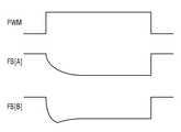
구체적으로, 보호 회로는 LED 어레이의 포워드 전압(VFB)을 측정하여 LED 어레이의 열화를 감지하는데, 종래의 보호 회로는 LED 어레이의 열화와 무관한 정전류원의 정착시간 또는 정전류의 피크 전류에 의한 비정상적인 포워드 전압(VFB)을 LED 어레이의 열화로 감지하는 문제점이 있었다.Specifically, the protection circuit measures the forward voltage (VFB ) of the LED array to detect the deterioration of the LED array. The conventional protection circuit is designed to prevent deterioration of the LED array due to the fixing time of the constant current source or the peak current of the constant current There is a problem that the abnormal forward voltage (VFB ) is detected by deterioration of the LED array.
구체적으로, 도 6을 참고하면, 디밍 신호(PWM)가 온 됨에 따라 LED 어레이에 전류가 흐르게 되어 포워드 전압(VFB)은 점차 떨어지게 된다. 그러나 정전류원의 정착시간이 느려 FB(A)와 같이 포워드 전압이 떨어지게 되는 경우, 종래의 보호 회로는 이러한 구간에서 포워드 전압을 측정하는 경우가 존재하였다. 그러나 이러한 구간에서 포워드 전압이 측정되면, 측정된 포워드 전압은 정상 포워드 전압보다 높아, 보호 회로는 해당 LED 어레이가 쇼트된 것으로 판단하였다.Specifically, referring to FIG. 6, as the dimming signal PWM is turned on, a current flows through the LED array, and the forward voltage VFB gradually drops. However, when the fixing time of the constant current source is so slow that the forward voltage drops like FB (A), the conventional protection circuit has a case where the forward voltage is measured in this section. However, when the forward voltage is measured in this section, the measured forward voltage is higher than the normal forward voltage and the protection circuit has determined that the LED array is shorted.
그리고 정전류의 피크 전류에 의하여 FB(B)와 같이 포워드 전압이 0V에 가깝게 떨어지게 되는 경우, 종래의 보호 회로는 이러한 구간에서 포워드 전압을 측정하는 경우가 존재하였다. 그러나 이러한 구간에서 포워드 전압이 측정되면, 측정된 포워드 전압은 정상 포워드 전압보다 낮아, 보호 회로는 LED 어레이가 오픈된 것으로 판단하였다.And, when the forward voltage drops close to 0V due to the peak current of the constant current like FB (B), the conventional protection circuit has a case where the forward voltage is measured in this section. However, if the forward voltage is measured in this interval, the measured forward voltage is lower than the normal forward voltage, and the protection circuit has determined that the LED array is open.
따라서, 본 발명의 목적은 LED 어레이의 열화를 정확하게 감지할 수 있는 LED 구동 장치를 제공하는 데 있다.Accordingly, it is an object of the present invention to provide an LED driving apparatus capable of accurately detecting deterioration of an LED array.
이상과 같은 목적을 달성하기 위한 본 발명에 따른 LED 구동장치는, LED 어레이의 구동을 위한 디밍 신호를 입력받는 입력부, 상기 입력된 디밍 신호의 온 구간을 확장하는 확장부, 상기 확장된 디밍 신호를 이용하여 상기 LED 어레이를 구동하는 LED 구동부, 및, 상기 입력된 디밍 신호의 하강 에지 시점에 상기 LED 어레이 및 상기 LED 구동부 사이의 포워드 전압을 측정하여 상기 LED 어레이의 열화를 감지하는 감지부를 포함한다.According to an aspect of the present invention, there is provided an LED driving apparatus including an input unit for receiving a dimming signal for driving an LED array, an expansion unit for expanding an ON period of the input dimming signal, And a sensing unit for sensing a deterioration of the LED array by measuring a forward voltage between the LED array and the LED driving unit at a falling edge of the input dimming signal.
이 경우, 상기 확장부는, 상기 입력된 디밍 신호를 지연하는 지연부, 및, 상기 입력된 디밍 신호와 상기 지연된 디밍 신호를 입력받아 확장된 디밍 신호를 출력하는 OR 게이트를 포함한다.In this case, the expansion unit includes a delay unit that delays the input dimming signal, and an OR gate that receives the input dimming signal and the delayed dimming signal and outputs an expanded dimming signal.
이 경우, 상기 지연부는, 상기 입력된 디밍 신호를 100ns 내지 1000ns 지연하는 것이 바람직하다.In this case, it is preferable that the delay unit delays the input dimming signal by 100 ns to 1000 ns.
한편, 상기 확장부는, 상기 디밍 신호가 100% 듀티 신호인 경우, 입력된 디밍 신호 대신에 기설정된 주파수를 갖는 클럭 신호를 상기 감지부에 제공하는 것이 바람직하다.Preferably, the extension unit provides the sensing unit with a clock signal having a predetermined frequency instead of the dimming signal when the dimming signal is a 100% duty signal.
이 경우, 상기 확장부는, 상기 디밍 신호가 100% 듀티 신호인지에 따라 상기 입력된 디밍 신호 및 기설정된 주파수를 갖는 클럭 신호 중 하나를 상기 감지부에 제공하는 멀티플렉서를 포함할 수 있다.In this case, the expansion unit may include a multiplexer for providing the sensing unit with one of the input dimming signal and the clock signal having a predetermined frequency according to whether the dimming signal is a 100% duty signal.
한편, 상기 클럭 신호는, 상기 LED 어레이의 구동 전압을 조정하기 위한 PWM 신호를 생성하는데 이용되는 클럭 신호인 것이 바람직하다.Preferably, the clock signal is a clock signal used to generate a PWM signal for adjusting a driving voltage of the LED array.
한편, 상기 감지부는, 상기 측정된 포워드 전압이 기설정된 제1 전압보다 작으면, 상기 LED 어레이가 오픈된 것으로 판단하고, 상기 측정된 포워드 전압이 기설정된 제2 전압보다 크면, 상기 LED 어레이가 쇼트된 것으로 판단하며, 상기 기설정된 제1 전압은, 상기 LED 어레이의 정상 동작시의 포워드 전압보다 작고, 상기 기설정된 제2 전압은, 상기 LED 어레이의 정상 동작시의 포워드 전압보다 큰 것이 바람직하다.Meanwhile, the sensing unit may determine that the LED array is open if the measured forward voltage is less than a predetermined first voltage, and if the measured forward voltage is greater than a predetermined second voltage, The predetermined first voltage is smaller than the forward voltage in the normal operation of the LED array and the predetermined second voltage is larger than the forward voltage in the normal operation of the LED array.
한편, 상기 감지부는, 상기 측정된 포워드 전압이 기설정된 제1 전압보다 작은지를 비교하는 제1 비교기, 상기 측정된 포워드 전압이 기설정된 제2 전압보다 큰지를 비교하는 제2 비교기, 상기 입력된 디밍 신호가 하강 에지인 경우에 상기 제1 비교기의 출력에 따라 상기 LED 어레이의 오픈 여부를 판단하는 제1 판단부, 및 상기 입력된 디밍 신호가 하강 에지인 경우에 상기 제2 비교기의 출력에 따라 상기 LED 어레이의 쇼트 여부를 판단하는 제2 판단부를 포함한다.The sensing unit may include a first comparator for comparing whether the measured forward voltage is less than a predetermined first voltage, a second comparator for comparing whether the measured forward voltage is greater than a predetermined second voltage, A first comparator for comparing the output of the first comparator with the output of the second comparator when the input dimming signal is on the falling edge, And a second determination unit for determining whether or not the LED array is short-circuited.
이 경우, 상기 제1 판단부는, 상기 입력된 디밍 신호를 반전하여 출력하는 제1 인버터, 및, 상기 제1 인버터의 반전된 디밍 신호를 클럭 신호로 입력받고, 상기 제1 비교기의 출력을 데이터 신호로 입력받는 제1 데이터 플리플롭을 포함하고, 상기 제2 판단부는, 상기 입력된 디밍 신호를 반정하여 출력하는 제2 인버터, 및, 상기 제2 인버터의 반전된 디밍 신호를 클럭 신호를 클럭 신호로 입력받고, 상기 제2 비교기의 출력을 데이터 신호로 입력받는 제2 데이터 플리플롭을 포함할 수 있다.In this case, the first determination unit may include: a first inverter that inverts the input dimming signal and outputs the inverted dimming signal; and a second comparator that receives the inverted dimming signal of the first inverter as a clock signal, The second inverter outputs the inverted dimming signal of the second inverter as a clock signal to the second inverter. The second inverter receives the input dimming signal, And a second data flip-flop receiving the output of the second comparator as a data signal.
한편, 상기 기설정된 제1 전압은, 상기 LED 어레이의 정상 동작시의 포워드 전압보다 작고, 상기 기설정된 제2 전압은, 상기 LED 어레이의 정상 동작시의 포워드 전압보다 큰 것이 바람직하다.Preferably, the predetermined first voltage is smaller than the forward voltage in the normal operation of the LED array, and the predetermined second voltage is larger than the forward voltage in normal operation of the LED array.
이와 같이 본 실시 예에 따른 LED 구동회로는, 포워드 전압의 비정상적인 구간을 배제한 영역에서 LED 어레이의 포워드 전압을 측정하는바, LED 어레이의 열화를 정확하게 감지할 수 있게 된다.As described above, the LED driving circuit according to the present embodiment measures the forward voltage of the LED array in the region excluding the abnormal period of the forward voltage, and thus can accurately detect the deterioration of the LED array.
도 1은 본 발명의 일 실시 예에 따른 LED 구동장치의 블록도,
도 2는 본 실시 예에 따른 복수의 LED 구동부의 회로도,
도 3은 도 1의 확장부의 구체적인 회로도,
도 4는 도 1의 감지부의 구체적인 회로도,
도 5는 도 3의 확장부의 동작을 설명하기 위한 파형도, 그리고,
도 6은 정전류원의 정착시간 또는 정전류의 피크 전류에 의한 비정상적인 포워드 전압의 변화를 설명하기 위한 파형도이다.1 is a block diagram of an LED driving apparatus according to an embodiment of the present invention;
2 is a circuit diagram of a plurality of LED driving units according to the present embodiment,
FIG. 3 is a specific circuit diagram of the extension of FIG. 1;
FIG. 4 is a specific circuit diagram of the sensing unit of FIG. 1;
FIG. 5 is a waveform diagram for explaining the operation of the extension of FIG. 3,
6 is a waveform diagram for explaining a change in an abnormal forward voltage due to a fixing time of a constant current source or a peak current of a constant current.
이하에서는 도면을 참조하여 본 발명을 보다 상세하게 설명한다.Hereinafter, the present invention will be described in detail with reference to the drawings.
도 1은 본 발명의 일 실시 예에 따른 LED 구동장치의 블록도이다.1 is a block diagram of an LED driving apparatus according to an embodiment of the present invention.
도 1을 참고하면, LED 구동장치(1000)는 입력부(100), PWM 신호 생성부(200), DC-DC 컨버터(300), LED 구동부(400), LED 어레이(500), 확장부(600) 및 감지부(700)를 포함한다.1, the
입력부(100)는 LED 어레이(500)의 구동을 위한 디밍 신호를 입력받는다. 구체적으로, LED에 대한 디지털 디밍 방법으로 다이렉트 모드(direct mode), 고정 위상 모드(fixed phase mode), 위상 이동 모드(phase shift mode)가 존재한다. 여기서, 다이렉트 모드는 PWM 주파수 및 온 듀티(On duty) 모두를 외부(PAD)에서 제어하는 방식이고, 고정 위상 모드 및 위상 이동 모드는 PWM 주파수는 IC 내부적으로 생성하고 온 듀티만 PAD에서 입력받아 제어하는 방식이다. 여기서 디밍 신호란, LED의 휘도와 색 온도 등을 조정하거나 온도 보상을 위한 신호이다. 한편, 본 실시 예에서는 디밍 신호를 외부로부터 입력받는 다이렉트 모드 방식에 대해서만 설명하였지만, 구현시에는 고정 위상 모드 및 위상 이동 모드와 같은 방식으로 구현될 수도 있다.The
PWM 신호 생성부(200)는 LED 어레이(500)의 전원을 조정하기 위한 PWM 신호를 생성한다. 구체적으로, PWM 신호 생성부(200)는 DC-DC 컨버터(300)의 구동 전압의 크기를 제어하기 위한 PWM 신호를 생성한다. 이러한 PWM 신호 생성부(200)는 기설정된 주파수를 갖는 클럭 신호를 기초로 클럭 신호의 온 구간을 확장하거나 축소하여 생성될 수 있다.The
DC-DC 컨버터(300)는 스위칭 동작을 수행하는 트랜지스터를 포함하고, 트랜지스터의 스위치 동작에 의하여 LED 어레이(500)에 구동 전압을 제공한다. 구체적으로, DC-DC 컨버터(300)는 PWM 신호 생성부(200)에서 생성된 PWM 신호에 기초하여 DC 전압을 컨버팅하고, 컨버팅된 DC 전압(즉, 구동 전압)을 LED 어레이(500)에 제공한다. 이때, DC-DC 컨버터(300)는 LED 어레이(500)가 포화 영역에서 동작하도록 LED 어레이(500)의 순방향 바이어스 전압에 대응하는 전압을 LED 어레이(500)에 제공할 수 있다.The DC-
LED 구동부(400)는 확장된 디밍 신호를 이용하여 LED 어레이(500)를 구동한다. 구체적으로, LED 구동부(400)는 후술할 확장부(600)에서 온 구간이 확장된 디밍 신호를 이용하여 LED 어레이(500) 내의 구동 전류를 조정할 수 있다. LED 구동부(400)의 구체적인 구성 및 동작은 도 2를 참고하여 후술한다.The
확장부(600)는 입력된 디밍 신호의 온 구간을 확장한다. 구체적으로, 확장부(600)는 입력부(100)를 통하여 입력된 디밍 신호의 온 구간을 100ns 내지 1000ns 지연하여 LED 구동부(400)에 제공할 수 있다. 확장부(600)의 구체적인 구성 및 동작에 대해서는 도 3을 참고하여 후술한다.The
감지부(700)는 입력된 디밍 신호의 하상 에지 시점에 LED 어레이(500)의 포워드 전압을 측정하여 LED 어레이(500)의 열화를 감지한다. 구체적으로, 감지부(700)는 입력된 디밍 신호가 하강 에지시에 측정된 포워드 전압이 기설정된 제1 전압보다 작으면, LED 어레이(500)가 오픈된 것으로 판단하고, 입력된 디밍 신호가 하강 에지시에 측정된 포워드 전압이 기설정된 제2 전압보다 크면, LED 어레이(500)가 쇼트된 것으로 판단할 수 있다. 여기서, 기설정된 제1 전압은, LED 어레이(500)의 정상 동작시의 포워드 전압보다 작은 전압이고, 기설정된 제2 전압은 LED 어레이(500)의 정상 동작시의 포워드 전압보다 큰 전압이다. 이러한 기설정된 제1 전압 및 제2 전압의 크기는 시스템마다 변경될 수 있으며, 제조사의 실험에 의하여 최적화된 전압 값이 선택될 수 있다.The
이상과 같이 본 실시 예에 따른 LED 구동장치(1000)는 포워드 전압이 가장 안정된 시점에서 그 크기를 측정하여 LED 어레이(500)의 열화를 감지하는바, 정전류원의 정착시간 또는 정전류의 피크 전류에 의해 발생하는 비정상적인 포워드 전압과 무관하게 LED 어레이(500)의 열화 여부를 정확하게 감지할 수 있게 된다.As described above, the
도 2는 본 실시 예에 따른 복수의 LED 구동부의 회로도이다.2 is a circuit diagram of a plurality of LED driving units according to the present embodiment.
도 2를 참고하면, LED 구동부(400)는 트랜지스터(410), 비교기(420), 저항(430) 및 복수의 스위칭부(440)로 구성될 수 있다.Referring to FIG. 2, the
트랜지스터(410)는 비교기(420)의 출력 신호 및 복수의 스위칭부(440)의 연결 상태에 따라 스위칭 동작을 수행한다. 구체적으로, 트랜지스터(410)는 드레인이 LED 어레이(500)의 일 단과 연결되고, 소스가 저항(430)과 연결되고, 게이트가 복수의 스위칭부(440)를 통하여 비교기(420)의 출력단에 연결된다. 한편, 본 실시 예에서는 n-MOS 트랜지스터를 이용하여 트랜지스터를 구현하는 예만을 도시하였지만, 구현시에는 다른 소자를 이용하여 구현할 수도 있다.The
비교기(420)는 스위칭부(410)와 저항(430)이 공통 접하는 공통 노드의 전압(VS)과 기설정된 기준 전압(VREF)을 비교하여 트랜지스터(410)를 제어한다. 구체적으로, 비교기(420)는 OP-AMP로 구현될 수 있으며, OP-AMP로 구현되는 경우, 양의 단자가 기준 전압(VREF)을 입력받고, 음의 단자가 저항(430)과 트랜지스터(410)가 공통 접하는 공통 노드의 전압(VS)을 입력받고, 출력단이 복수의 스위칭부(440)를 통하여 트랜지스터(410)의 게이트에 연결된다.The
저항(430)은 일 단이 트랜지스터(410)의 소스와 연결되고, 타 단이 접지된다.One end of the
복수의 스위칭부(440)는 확장된 디밍 신호에 따라 비교기(420)의 출력 신호를 선택적으로 트랜지스터(410)에 제공한다. 구체적으로, 복수의 스위칭부(440)는 제1 스위치(441), 제2 스위치(442), 제3 스위치(443), 제4 스위치(444)를 포함한다.The plurality of switching units 440 selectively provide the output signal of the
제1 스위치(441)는 비교기(420)와 트랜지스터(410)의 게이트 사이에 배치되며, 확장된 디밍 신호가 온(on)되면 연결되고, 확장된 디밍 신호가 오프(off)되면 개방된다.The
제2 스위치(442)는 트랜지스터(420)의 소스와 저항(430)이 공통 접하는 공통 노드와 비교기(420)의 음의 단자 사이에 배치되며, 확장된 디밍 신호가 온(on)되면 연결되고, 확장된 디밍 신호가 오프(off)되면 개방된다.The
제3 스위치(443)는 트랜지스터(420)의 음의 단자와 트랜지스터(420)의 출력단 사이에 배치되며, 확장된 디밍 신호가 온(on) 되면 개방되고, 확장된 디밍 신호가 오프(off)되면 연결된다.The
제4 스위치(442)는 트랜지스터(420)의 게이트와 접지단 사이에 배치되며, 확장된 디밍 신호가 온(on) 되면 개방되고, 확장된 디밍 신호가 오프(off)되면 연결된다.The
따라서, 확장된 디밍 신호가 온(on)되면, 제1 스위치(441) 및 제2 스위치(442)는 연결되고, 제3 스위치(443) 및 제4 스위치(444)는 개방되는바, 비교기(420)는 스위칭부(410)와 저항(430)이 공통 접하는 공통 노드의 전압(VS)과 기설정된 기준 전압(VREF)을 비교하여 트랜지스터(410)를 제어한다.Thus, when the extended dimming signal is turned on, the
반대로 확장된 디밍 신호가 오프(off)되면, 제1 스위치(441) 및 제2 스위치(442)는 개방되고, 제3 스위치(443) 및 제4 스위치(444)는 연결되는바, 트랜지스터(410)의 게이트는 접지단에 연결되어 트랜지스터(410)는 LED 어레이(500)에 정전류 공급을 차단한다.Conversely, when the extended dimming signal is turned off, the
도 3은 도 1의 확장부의 구체적인 회로도이다.3 is a specific circuit diagram of the extension of FIG.
도 3을 참고하면, 확장부(600)는 멀티플렉서(611), 지연부(613) 및 OR 게이트(615)로 구성된다.3, the
멀티플렉서(611)는 입력된 디밍 신호(PWM)가 100% 듀티 신호인지에 따라 입력된 디밍 신호 및 기설정된 주파수를 갖는 클럭 신호 중 하나를 감지부(700)에 제공한다. 구체적으로, 감지부(700)는 디밍 신호의 하강 에지에서 포워드 전압을 측정하나, 디밍 신호(PWM)가 100% 듀티 신호인 경우, 하강 에지가 존재하지 않게 된다.The
따라서, 멀티플렉서(611)는 입력된 디밍 신호(PWM)가 100% 듀티 신호인 경우, LED 구동 장치(1000) 내부의 클럭 신호를 입력된 디밍 신호 대신에 감지부(700)에 제공할 수 있다. 도 3을 도시하고 설명함에 있어서, 디밍 신호가 100% 듀티 신호인지 아닌지를 알리는 신호를 멀티플렉서(611)의 제어 신호로 입력받는 형태만을 설명하였지만, 즉, 입력된 디밍 신호가 100% 듀티 신호인지에 대한 판단이 다른 구성에서 수행되는 형태로 설명하였지만, 구현시에 입력된 디밍 신호가 100% 듀티 신호인지 여부는 확장부(600) 자체에서 판단하는 형태로도 구현될 수 있다.Accordingly, the
여기서 클럭 신호는 LED 어레이(500)의 구동 전압을 조정하기 위한 PWM 신호를 생성하는데 이용되는 클럭 신호이다. 즉, PWM 신호 생성부(200)에서 PWM 신호 생성시 이용되는 클록 신호이다.Where the clock signal is a clock signal that is used to generate a PWM signal for adjusting the drive voltage of the
지연부(613)는 입력부(100)에서 입력된 디밍 신호를 지연한다. 이때 지연부(613)는 입력된 디밍 신호를 100ns 내지 1000ns 범위에서 지연할 수 있다.The
OR 게이트(615)는 입력된 디밍 신호와 지연된 디밍 신호를 입력받아 확장된 디밍 신호를 출력한다. 구체적으로, OR 게이트(615)는 입력된 디밍 신호 및 지연부(613)의 출력을 입력받고, 입력된 디밍 신호와 지연된 디밍 신호의 논리합을 확장된 디밍 신호로 출력할 수 있다.The OR
이와 같은 구성에 의하여, 확장부(600)는 입력부(100)에서 입력된 디밍 신호의 온 구간을 확장하여 출력할 수 있다.With such a configuration, the
도 4는 도 1의 감지부의 구체적인 회로도이다.4 is a specific circuit diagram of the sensing unit of FIG.
도 4를 참고하면, 감지부(700)는 제1 비교기(710-1), 제2 비교기(710-2), 제1 판단부(720-1), 제2 판단부(720-2)를 포함한다.4, the
제1 비교기(710-1)는 측정된 포워드 전압이 기설정된 제1 전압보다 작은지를 비교한다. 구체적으로, 제1 비교기(710-1)는 LED 어레이(500)의 포워드 전압을 음의 단자로 입력받고, 기설정된 제1 전압을 양의 단자로 입력받아 그 차이를 출력하는 OP-AMP로 구현될 수 있다. 여기서 기설정된 제1 전압은 LED 어레이(500)의 정상 동작시의 포워드 전압보다 작은 전압이다.The first comparator 710-1 compares whether the measured forward voltage is less than a predetermined first voltage. Specifically, the first comparator 710-1 is implemented as an OP-AMP that receives a forward voltage of the
제2 비교기(710-2)는 측정된 포워드 전압이 기설정된 제2 전압보다 큰지를 비교한다. 구체적으로, 제2 비교기(710-2)는 LED 어레이(500)의 포워드 전압을 양의 단자로 입력받고, 기설정된 제2 전압을 음의 단자로 입력받아 그 차이를 출력하는 OP-AMP로 구현될 수 있다. 여기서 기설정된 제2 전압은 LED 어레이(500)의 정상 동작시의 포워드 전압보다 큰 전압이다.The second comparator 710-2 compares the measured forward voltage with a predetermined second voltage. Specifically, the second comparator 710-2 is implemented as an OP-AMP that receives a forward voltage of the
제1 판단부(720-1)는 입력된 디밍 신호가 하강 에지인 경우에 제1 비교기(710-1)의 출력에 따라 LED 어레이(500)의 오픈 여부를 판단한다. 구체적으로, 제1 판단부(720-1)는 제1 인버터 및 제1 데이터 플리플롭으로 구현될 수 있다.The first determination unit 720-1 determines whether the
제1 인버터는 입력된 디밍 신호를 반전하여 출력한다.The first inverter inverts the input dimming signal and outputs it.
제1 데이터 플리플롭은 제1 인버터의 반전된 디밍 신호를 클럭 신호로 입력받고, 제1 비교기(710-1)의 출력을 데이터 신호로 입력받는다. 따라서, 제1 데이터 플리플롭은 확장된 디밍 신호가 끝나기 직전(구체적으로, 확장된 디밍 신호의 하강 에지로부터 지연부(613)의 지연시간 전)에 포워드 전압이 오픈된 상태의 전압인지를 판단할 수 있다.The first data flip-flop receives the inverted dimming signal of the first inverter as a clock signal and receives the output of the first comparator 710-1 as a data signal. Therefore, the first data flip-flop judges whether or not the forward voltage is in the open state immediately before the end of the extended dimming signal (specifically, before the delay time of the
제2 판단부(720-2)는 입력된 디밍 신호가 하강 에지인 경우에 제2 비교기(710-2)의 출력에 따라 LED 어레이(500)의 쇼트 여부를 판단한다. 구체적으로, 제2 판단부(720-2)는 제2 인버터 및 제2 데이터 플리플롭으로 구현될 수 있다.The second determination unit 720-2 determines whether the
제2 인버터는 입력된 디밍 신호를 반전하여 출력한다.The second inverter inverts the input dimming signal and outputs it.
제2 데이터 플리플롭은 제2 인버터의 반전된 디밍 신호를 클럭 신호로 입력받고, 제2 비교기(720-2)의 출력을 데이터 신호로 입력받는다. 따라서, 제2 데이터 플리플롭은 확장된 디밍 신호가 끝나기 직전(구체적으로, 확장된 디밍 신호의 하강 에지로부터 지연부(613)의 지연시간 전)에 포워드 전압이 오픈된 상태의 전압인지를 판단할 수 있다.The second data flip-flop receives the inverted dimming signal of the second inverter as a clock signal and receives the output of the second comparator 720-2 as a data signal. Therefore, the second data flip-flop judges whether or not the forward voltage is in the open state immediately before the end of the extended dimming signal (specifically, before the delay time of the
본 실시 예에서는 데이터 플리플롭을 이용하여 판단부(720-1, 720-2)를 구현하였지만, 구현시에는 데이터 플리플롭 이외의 다른 플리플롭을 이용하여 판단부(720)를 구현할 수도 있다. 또한, 판단부(720) 각각이 별도의 인버터를 이용하는 것으로 도시하고 설명하였지만, 제1 플리플롭 및 제2 플리플롭은 동일한 신호를 클럭으로 입력받는다는 점에서, 하나의 인버터를 이용하여 판단부(720-1, 720-2)를 구현할 수 있다.Although the determination flags 720-1 and 720-2 are implemented using the data flip-flop in this embodiment, the determination unit 720 may be implemented using flip-flops other than the data flip-flops at the time of implementation. In addition, although each of the determination units 720 has been illustrated and described as using a separate inverter, the first flip-flop and the second flip-flop may be connected to the determination unit 720 -1, 720-2).
도 5는 도 3의 확장부의 동작을 설명하기 위한 파형도이다.5 is a waveform diagram for explaining the operation of the extension of FIG.
LED 어레이(500)의 포워드 전압은 LED 어레이의 구동 정지 직전이 가장 안정적인 전압을 갖는다. 즉, 디밍 신호의 하강 에지 직전에 가장 안정적인 전압을 갖는다. 그러나 디밍 신호가 언제 하이 신호에서 로우 신호로 변경될 것인지 예측하는 것은 불가능하기 때문에, 본 실시 예에서는 디밍 신호의 온 구간을 도 5에 도시된 바와 같이 소폭 확장하고, 확장된 디밍 신호를 LED 구동부(400)에 제공한다.The forward voltage of the
이와 같은 구성에 의하여 본 실시 예에 따른 LED 구동 장치(1000)는 확장된 디밍 신호의 하강 에지 직전(즉, 입력된 디밍 신호의 하강 에지 시)에 포워드 전압을 측정하여 LED 어레이의 열화 여부를 감지할 수 있다. 한편, 도 5에는 확장된 디밍 신호와 입력된 디밍 신호의 차이를 구분하기 위하여, 두 신호의 변화가 크게 나는 형태로 도시하였으나, 상술한 바와 같이 확장부(600)는 입력된 디밍 신호를 100ns 내지 1000ns의 시간만큼만 확장하는바, 이에 따른 LED 구동부(400)의 동작 변화는 미미하다.With such a configuration, the
그리고 디밍 신호가 100% 듀티 신호인 경우, 확장된 디밍 신호(PWMD_IN) 역시 100% 듀티 신호임을 확인할 수 있다. 이때, 확장부는 기설정된 주파수를 갖는 클럭 신호를 감지부(700)에 디밍 신호로 제공함을 확인할 수 있다.If the dimming signal is a 100% duty signal, the extended dimming signal PWMD_IN is also a 100% duty signal. At this time, it can be confirmed that the expansion unit provides the clock signal having the preset frequency to the
도 1 내지 도 5를 설명함에 있어서, 하나의 LED 어레이(500)에 대한 열화를 감지하는 것만을 설명하였으나, 구현시에 LED 구동장치는 복수의 LED 어레이를 구동하는 형태로도 구현할 수 있다. 이때, LED 구동장치는 복수의 LED 어레이 각각의 열화를 감지하는 형태로 구현할 수 있다.In the description of FIGS. 1 to 5, only the deterioration of one
이상에서는 본 발명의 바람직한 실시 예에 대하여 도시하고 설명하였지만, 본 발명은 상술한 특정의 실시 예에 한정되지 아니하며, 청구범위에서 청구하는 본 발명의 요지를 벗어남이 없이 당해 발명이 속하는 기술분야에서 통상의 지식을 가진자에 의해 다양한 변형실시가 가능한 것은 물론이고, 이러한 변형 실시들은 본 발명의 기술적 사상이나 전망으로부터 개별적으로 이해되어 져서는 안 될 것이다.While the present invention has been particularly shown and described with reference to exemplary embodiments thereof, it is clearly understood that the same is by way of illustration and example only and is not to be construed as limiting the scope of the invention as defined by the appended claims. It will be understood by those skilled in the art that various changes in form and details may be made therein without departing from the spirit and scope of the present invention.
1000: LED 구동장치100: 입력부
200: PWM 신호 생성부300: DC-DC 컨버터
400: LED 구동부500: LED 어레이
600: 확장부700: 감지부1000: LED driving device 100: input part
200: PWM signal generator 300: DC-DC converter
400: LED driver 500: LED array
600: Extension unit 700:
Claims (10)
Translated fromKoreanLED 어레이의 구동을 위한 디밍 신호를 입력받는 입력부;
상기 입력된 디밍 신호의 온 구간을 확장하는 확장부;
상기 확장된 디밍 신호를 이용하여 상기 LED 어레이를 구동하는 LED 구동부; 및
상기 입력된 디밍 신호의 하강 에지 시점에 상기 LED 어레이 및 상기 LED 구동부 사이의 포워드 전압을 측정하여 상기 LED 어레이의 열화를 감지하는 감지부를 포함하고
상기 감지부는 상기 확장된 디밍신호에 의해 상기 LED 구동부가 동작할 때, 상기 입력된 디밍 신호의 하강 에지 시점에 측정된 포워드 전압을 이용하여 상기 LED 어레이의 오픈 또는 쇼트 여부를 판단하는 것을 특징으로 하는 LED 구동장치In the LED driving device,
An input unit for receiving a dimming signal for driving the LED array;
An expansion unit for expanding the ON period of the input dimming signal;
An LED driver driving the LED array using the extended dimming signal; And
And a sensing unit for sensing a deterioration of the LED array by measuring a forward voltage between the LED array and the LED driving unit at a falling edge of the input dimming signal
Wherein the sensing unit determines whether the LED array is open or shorted by using a forward voltage measured at a falling edge of the input dimming signal when the LED driver operates according to the extended dimming signal LED driver
상기 확장부는,
상기 입력된 디밍 신호를 지연하는 지연부; 및
상기 입력된 디밍 신호와 상기 지연된 디밍 신호를 입력받아 확장된 디밍 신호를 출력하는 OR 게이트;를 포함하는 LED 구동장치.The method according to claim 1,
Wherein the expanding portion comprises:
A delay unit for delaying the input dimming signal; And
And an OR gate for receiving the input dimming signal and the delayed dimming signal to output an expanded dimming signal.
상기 지연부는,
상기 입력된 디밍 신호를 100ns 내지 1000ns 지연하는 것을 특징으로 하는 LED 구동장치.3. The method of claim 2,
Wherein the delay unit comprises:
And delays the input dimming signal by 100 ns to 1000 ns.
상기 확장부는,
상기 디밍 신호가 100% 듀티 신호인 경우, 입력된 디밍 신호 대신에 기설정된 주파수를 갖는 클럭 신호를 상기 감지부에 제공하는 것을 특징으로 하는 LED 구동장치.The method according to claim 1,
Wherein the expanding portion comprises:
Wherein when the dimming signal is a 100% duty signal, a clock signal having a predetermined frequency is provided to the sensing unit instead of the dimming signal.
상기 확장부는,
상기 디밍 신호가 100% 듀티 신호인지에 따라 상기 입력된 디밍 신호 및 기설정된 주파수를 갖는 클럭 신호 중 하나를 상기 감지부에 제공하는 멀티플렉서;를 포함하는 것을 특징으로 하는 LED 구동장치.5. The method of claim 4,
Wherein the expanding portion comprises:
And a multiplexer for providing the sensing unit with one of the input dimming signal and a clock signal having a predetermined frequency according to whether the dimming signal is a 100% duty signal.
상기 클럭 신호는,
상기 LED 어레이의 구동 전압을 조정하기 위한 PWM 신호를 생성하는데 이용되는 클럭 신호인 것을 특징으로 하는 LED 구동장치.5. The method of claim 4,
The clock signal,
Wherein the LED driver is a clock signal used to generate a PWM signal for adjusting a driving voltage of the LED array.
상기 감지부는,
상기 측정된 포워드 전압이 기설정된 제1 전압보다 작으면, 상기 LED 어레이가 오픈된 것으로 판단하고,
상기 측정된 포워드 전압이 기설정된 제2 전압보다 크면, 상기 LED 어레이가 쇼트된 것으로 판단하며,
상기 기설정된 제1 전압은, 상기 LED 어레이의 정상 동작시의 포워드 전압보다 작고,
상기 기설정된 제2 전압은, 상기 LED 어레이의 정상 동작시의 포워드 전압보다 큰 것을 특징으로 하는 LED 구동장치.The method according to claim 1,
The sensing unit includes:
If the measured forward voltage is smaller than a predetermined first voltage, determines that the LED array is open,
Determines that the LED array is shorted if the measured forward voltage is greater than a predetermined second voltage,
Wherein the predetermined first voltage is smaller than a forward voltage at the time of normal operation of the LED array,
Wherein the predetermined second voltage is greater than a forward voltage during normal operation of the LED array.
상기 감지부는,
상기 측정된 포워드 전압이 기설정된 제1 전압보다 작은지를 비교하는 제1 비교기;
상기 측정된 포워드 전압이 기설정된 제2 전압보다 큰지를 비교하는 제2 비교기;
상기 입력된 디밍 신호가 하강 에지인 경우에 상기 제1 비교기의 출력에 따라 상기 LED 어레이의 오픈 여부를 판단하는 제1 판단부; 및
상기 입력된 디밍 신호가 하강 에지인 경우에 상기 제2 비교기의 출력에 따라 상기 LED 어레이의 쇼트 여부를 판단하는 제2 판단부;를 포함하는 것을 특징으로 하는 LED 구동장치.The method according to claim 1,
The sensing unit includes:
A first comparator for comparing whether the measured forward voltage is less than a predetermined first voltage;
A second comparator for comparing whether the measured forward voltage is greater than a predetermined second voltage;
A first determination unit for determining whether the LED array is open according to an output of the first comparator when the input dimming signal is a falling edge; And
And a second determination unit determining whether the LED array is short-circuited according to an output of the second comparator when the input dimming signal is a falling edge.
상기 제1 판단부는,
상기 입력된 디밍 신호를 반전하여 출력하는 제1 인버터; 및
상기 제1 인버터의 반전된 디밍 신호를 클럭 신호로 입력받고, 상기 제1 비교기의 출력을 데이터 신호로 입력받는 제1 데이터 플리플롭;을 포함하고,
상기 제2 판단부는,
상기 입력된 디밍 신호를 반정하여 출력하는 제2 인버터; 및
상기 제2 인버터의 반전된 디밍 신호를 클럭 신호를 클럭 신호로 입력받고, 상기 제2 비교기의 출력을 데이터 신호로 입력받는 제2 데이터 플리플롭;을 포함하는 것을 특징으로 하는 LED 구동장치.9. The method of claim 8,
The first determination unit may determine,
A first inverter for inverting and outputting the input dimming signal; And
And a first data flip-flop receiving the inverted dimming signal of the first inverter as a clock signal and receiving the output of the first comparator as a data signal,
The second determination unit may determine,
A second inverter for inverting the input dimming signal to output the dimming signal; And
And a second data flip-flop receiving the inverted dimming signal of the second inverter as a clock signal and receiving the output of the second comparator as a data signal.
상기 기설정된 제1 전압은,
상기 LED 어레이의 정상 동작시의 포워드 전압보다 작고,
상기 기설정된 제2 전압은,
상기 LED 어레이의 정상 동작시의 포워드 전압보다 큰 것을 특징으로 하는 LED 구동장치.9. The method of claim 8,
The predetermined first voltage may be a predetermined voltage,
A forward voltage lower than a forward voltage during normal operation of the LED array,
The predetermined second voltage may be a predetermined voltage,
Wherein the forward voltage of the LED array is greater than the forward voltage of the LED array during normal operation.
Priority Applications (4)
| Application Number | Priority Date | Filing Date | Title |
|---|---|---|---|
| KR1020110087461AKR101971287B1 (en) | 2011-08-30 | 2011-08-30 | Led driver apparatus |
| US13/586,059US9271369B2 (en) | 2011-08-30 | 2012-08-15 | LED driver apparatus |
| TW101131244ATWI563869B (en) | 2011-08-30 | 2012-08-28 | Led driver apparatus |
| CN201210315752.8ACN102968959B (en) | 2011-08-30 | 2012-08-30 | LED drives equipment, liquid crystal display and the method for driving LED backlight unit |
Applications Claiming Priority (1)
| Application Number | Priority Date | Filing Date | Title |
|---|---|---|---|
| KR1020110087461AKR101971287B1 (en) | 2011-08-30 | 2011-08-30 | Led driver apparatus |
Publications (2)
| Publication Number | Publication Date |
|---|---|
| KR20130024183A KR20130024183A (en) | 2013-03-08 |
| KR101971287B1true KR101971287B1 (en) | 2019-04-23 |
Family
ID=47743045
Family Applications (1)
| Application Number | Title | Priority Date | Filing Date |
|---|---|---|---|
| KR1020110087461AActiveKR101971287B1 (en) | 2011-08-30 | 2011-08-30 | Led driver apparatus |
Country Status (4)
| Country | Link |
|---|---|
| US (1) | US9271369B2 (en) |
| KR (1) | KR101971287B1 (en) |
| CN (1) | CN102968959B (en) |
| TW (1) | TWI563869B (en) |
Families Citing this family (17)
| Publication number | Priority date | Publication date | Assignee | Title |
|---|---|---|---|---|
| US9101020B2 (en)* | 2013-07-15 | 2015-08-04 | Luxmill Electronic Co., Ltd. | LED driver capable of regulating power dissipation and LED lighting apparatus using same |
| CN108601169B (en)* | 2013-08-09 | 2020-01-10 | 意法半导体研发(深圳)有限公司 | Driving apparatus for light emitting device and method thereof |
| CN104112431B (en)* | 2014-07-21 | 2016-08-17 | 康佳集团股份有限公司 | Use circuit and the driving method thereof of chip microcontroller multichannel backlight drive |
| TWI560679B (en) | 2014-12-01 | 2016-12-01 | Hon Hai Prec Ind Co Ltd | Backlight driving module and display device using the same |
| US9471078B1 (en)* | 2015-03-31 | 2016-10-18 | Qualcomm Incorporated | Ultra low power low drop-out regulators |
| KR102276226B1 (en)* | 2015-04-20 | 2021-07-19 | 삼성전자주식회사 | Light emitting diode driver circuit and method for light emitting diode driving |
| CN106328096A (en)* | 2015-07-07 | 2017-01-11 | 宇龙计算机通信科技(深圳)有限公司 | Backlight compensation method and device |
| JP6585989B2 (en)* | 2015-10-08 | 2019-10-02 | ローム株式会社 | Light emitting element driving device |
| CN105592595B (en)* | 2016-03-08 | 2017-06-27 | 深圳市华星光电技术有限公司 | backlight dimming circuit and liquid crystal display |
| TWI654903B (en) | 2017-12-21 | 2019-03-21 | 友達光電股份有限公司 | Light-emitting diode driving device and driving method thereof |
| TWI706395B (en)* | 2019-01-25 | 2020-10-01 | 友達光電股份有限公司 | Pixel circuit and detection method thereof |
| EP3715885B1 (en)* | 2019-03-29 | 2025-05-28 | MARELLI AUTOMOTIVE LIGHTING ITALY S.p.A. | Automobile lighting unit with oled light sources and related operating method |
| DE102021102543A1 (en)* | 2020-02-07 | 2021-08-12 | Analog Devices International Unlimited Company | Transconductance circuits and methods |
| US11272598B2 (en)* | 2020-02-07 | 2022-03-08 | Analog Devices International Unlimited Company | Transconductance circuits and methods |
| KR102687945B1 (en)* | 2020-02-12 | 2024-07-25 | 삼성디스플레이 주식회사 | Power voltage generator, method of controlling the same and display apparatus having the same |
| US12094430B2 (en)* | 2020-02-27 | 2024-09-17 | Nippon Seiki Co., Ltd. | Field-sequential projector device, head-up display device, program, and voltage measurement method |
| CN115188330B (en)* | 2022-09-13 | 2022-12-23 | 惠科股份有限公司 | Drive current adjusting circuit, color shift correction method, device, and storage medium |
Citations (5)
| Publication number | Priority date | Publication date | Assignee | Title |
|---|---|---|---|---|
| JP2005324656A (en)* | 2004-05-13 | 2005-11-24 | Toyota Motor Corp | Vehicle headlamp device |
| JP2008166981A (en)* | 2006-12-27 | 2008-07-17 | Matsushita Electric Ind Co Ltd | Delay adjustment circuit and delay adjustment method |
| US20100327872A1 (en)* | 2007-11-23 | 2010-12-30 | Industrial Technology Research Institute | Devices And Methods For LED Life Test |
| JP2011009011A (en)* | 2009-06-24 | 2011-01-13 | Panasonic Electric Works Co Ltd | Lighting system |
| JP2011113794A (en)* | 2009-11-26 | 2011-06-09 | Toshiba Lighting & Technology Corp | Led lighting apparatus and illuminating device |
Family Cites Families (21)
| Publication number | Priority date | Publication date | Assignee | Title |
|---|---|---|---|---|
| EP0869618B1 (en)* | 1997-04-02 | 2006-06-07 | Koninklijke Philips Electronics N.V. | Synchronisation circuit |
| US20030071821A1 (en)* | 2001-10-11 | 2003-04-17 | Sundahl Robert C. | Luminance compensation for emissive displays |
| EP1704752A4 (en)* | 2003-12-11 | 2009-09-23 | Philips Solid State Lighting | Thermal management methods and apparatus for lighting devices |
| CN101433130A (en)* | 2006-04-24 | 2009-05-13 | 松下电器产业株式会社 | Backlight control unit and display unit |
| KR100902219B1 (en)* | 2007-12-05 | 2009-06-11 | 삼성모바일디스플레이주식회사 | Organic light emitting display |
| US8106604B2 (en)* | 2008-03-12 | 2012-01-31 | Freescale Semiconductor, Inc. | LED driver with dynamic power management |
| US7550934B1 (en) | 2008-04-02 | 2009-06-23 | Micrel, Inc. | LED driver with fast open circuit protection, short circuit compensation, and rapid brightness control response |
| JP4743246B2 (en)* | 2008-09-25 | 2011-08-10 | カシオ計算機株式会社 | Projection device, projection device control program, and light source control method |
| TWI390490B (en)* | 2008-12-03 | 2013-03-21 | Au Optronics Corp | Light emitting diode backlight module and driving apparatus and method thereof |
| KR101581429B1 (en)* | 2009-05-25 | 2015-12-31 | 삼성디스플레이 주식회사 | Display device |
| US8305004B2 (en)* | 2009-06-09 | 2012-11-06 | Stmicroelectronics, Inc. | Apparatus and method for constant power offline LED driver |
| US8125161B2 (en)* | 2009-06-19 | 2012-02-28 | Samsung Electro-Mechanics Co., Ltd. | Light emitting device driving apparatus and method for driving the same |
| KR101578214B1 (en)* | 2009-08-04 | 2015-12-16 | 엘지디스플레이 주식회사 | Liquid crystal display and driving method thereof |
| TWI419609B (en)* | 2009-08-19 | 2013-12-11 | Novatek Microelectronics Corp | Led device with simultaneous open and short detection function and method thereof |
| KR20110024102A (en)* | 2009-09-01 | 2011-03-09 | 삼성전자주식회사 | LED driving apparatus and method, LED driving system and liquid crystal display using the same |
| US8334662B2 (en)* | 2009-09-11 | 2012-12-18 | Iwatt Inc. | Adaptive switch mode LED driver |
| US8193741B2 (en)* | 2009-12-24 | 2012-06-05 | Nxp B.V. | Boosting driver circuit for light-emitting diodes |
| US8373364B2 (en)* | 2009-12-29 | 2013-02-12 | Atmel Corporation | Smart monitoring of light emitting diode strings |
| CN201667742U (en)* | 2010-01-22 | 2010-12-08 | 青岛海信电器股份有限公司 | LED backlight driving device of light emitting diode and liquid crystal display |
| US8198832B2 (en)* | 2010-08-13 | 2012-06-12 | Linear Technology Corporation | Method and system for extending PWM dimming range in LED drivers |
| US9265104B2 (en)* | 2011-07-06 | 2016-02-16 | Allegro Microsystems, Llc | Electronic circuits and techniques for maintaining a consistent power delivered to a load |
- 2011
- 2011-08-30KRKR1020110087461Apatent/KR101971287B1/enactiveActive
- 2012
- 2012-08-15USUS13/586,059patent/US9271369B2/enactiveActive
- 2012-08-28TWTW101131244Apatent/TWI563869B/enactive
- 2012-08-30CNCN201210315752.8Apatent/CN102968959B/enactiveActive
Patent Citations (5)
| Publication number | Priority date | Publication date | Assignee | Title |
|---|---|---|---|---|
| JP2005324656A (en)* | 2004-05-13 | 2005-11-24 | Toyota Motor Corp | Vehicle headlamp device |
| JP2008166981A (en)* | 2006-12-27 | 2008-07-17 | Matsushita Electric Ind Co Ltd | Delay adjustment circuit and delay adjustment method |
| US20100327872A1 (en)* | 2007-11-23 | 2010-12-30 | Industrial Technology Research Institute | Devices And Methods For LED Life Test |
| JP2011009011A (en)* | 2009-06-24 | 2011-01-13 | Panasonic Electric Works Co Ltd | Lighting system |
| JP2011113794A (en)* | 2009-11-26 | 2011-06-09 | Toshiba Lighting & Technology Corp | Led lighting apparatus and illuminating device |
Also Published As
| Publication number | Publication date |
|---|---|
| CN102968959B (en) | 2016-10-26 |
| CN102968959A (en) | 2013-03-13 |
| TWI563869B (en) | 2016-12-21 |
| TW201315285A (en) | 2013-04-01 |
| US20130050288A1 (en) | 2013-02-28 |
| KR20130024183A (en) | 2013-03-08 |
| US9271369B2 (en) | 2016-02-23 |
Similar Documents
| Publication | Publication Date | Title |
|---|---|---|
| KR101971287B1 (en) | Led driver apparatus | |
| KR101955034B1 (en) | Detecting ciurcuit for short of led array and led driver apparatus having the same in | |
| KR101875220B1 (en) | Led driver circuit | |
| KR101941286B1 (en) | Led driver apparatus | |
| KR101847211B1 (en) | Led driver apparatus | |
| US8624524B2 (en) | Power management and control module and liquid crystal display device | |
| KR101565937B1 (en) | Backlight assembly display apparatus comprising the same and driving method of the display apparatus | |
| KR101113395B1 (en) | Light emitting diode driver | |
| EP2555589A1 (en) | Apparatus and method for controlling led driving circuit and apparatus and method for driving led | |
| KR101974218B1 (en) | Led driver apparatus | |
| KR20120095245A (en) | Pwm controlling circuit and led driver circuit having the same in | |
| KR101674217B1 (en) | Vref generating circuit and led driver circuit having the same in | |
| KR20130063863A (en) | Detecting ciurcuit for open of led array and led driver apparatus having the same in | |
| KR101978509B1 (en) | Led driver apparatus | |
| KR101977989B1 (en) | Led driver apparatus | |
| KR20180135431A (en) | Detecting ciurcuit for open of led array and led driver apparatus having the same in | |
| KR102051733B1 (en) | Led driver circuit |
Legal Events
| Date | Code | Title | Description |
|---|---|---|---|
| PA0109 | Patent application | Patent event code:PA01091R01D Comment text:Patent Application Patent event date:20110830 | |
| PG1501 | Laying open of application | ||
| A201 | Request for examination | ||
| PA0201 | Request for examination | Patent event code:PA02012R01D Patent event date:20160615 Comment text:Request for Examination of Application Patent event code:PA02011R01I Patent event date:20110830 Comment text:Patent Application | |
| E902 | Notification of reason for refusal | ||
| PE0902 | Notice of grounds for rejection | Comment text:Notification of reason for refusal Patent event date:20170919 Patent event code:PE09021S01D | |
| E902 | Notification of reason for refusal | ||
| PE0902 | Notice of grounds for rejection | Comment text:Notification of reason for refusal Patent event date:20180528 Patent event code:PE09021S01D | |
| E902 | Notification of reason for refusal | ||
| PE0902 | Notice of grounds for rejection | Comment text:Notification of reason for refusal Patent event date:20181129 Patent event code:PE09021S01D | |
| E701 | Decision to grant or registration of patent right | ||
| PE0701 | Decision of registration | Patent event code:PE07011S01D Comment text:Decision to Grant Registration Patent event date:20190320 | |
| GRNT | Written decision to grant | ||
| PR0701 | Registration of establishment | Comment text:Registration of Establishment Patent event date:20190416 Patent event code:PR07011E01D | |
| PR1002 | Payment of registration fee | Payment date:20190416 End annual number:3 Start annual number:1 | |
| PG1601 | Publication of registration | ||
| PR1001 | Payment of annual fee | Payment date:20220401 Start annual number:4 End annual number:4 | |
| PR1001 | Payment of annual fee | Payment date:20240325 Start annual number:6 End annual number:6 | |
| PR1001 | Payment of annual fee | Payment date:20250325 Start annual number:7 End annual number:7 |