KR101968929B1 - Sensor substrate, method of manufacturing the same and sensing display panel having the same - Google Patents
Sensor substrate, method of manufacturing the same and sensing display panel having the sameDownload PDFInfo
- Publication number
- KR101968929B1 KR101968929B1KR1020120100387AKR20120100387AKR101968929B1KR 101968929 B1KR101968929 B1KR 101968929B1KR 1020120100387 AKR1020120100387 AKR 1020120100387AKR 20120100387 AKR20120100387 AKR 20120100387AKR 101968929 B1KR101968929 B1KR 101968929B1
- Authority
- KR
- South Korea
- Prior art keywords
- electrode
- layer
- unit
- pattern
- color filter
- Prior art date
- Legal status (The legal status is an assumption and is not a legal conclusion. Google has not performed a legal analysis and makes no representation as to the accuracy of the status listed.)
- Active
Links
Images


Classifications
- G—PHYSICS
- G02—OPTICS
- G02F—OPTICAL DEVICES OR ARRANGEMENTS FOR THE CONTROL OF LIGHT BY MODIFICATION OF THE OPTICAL PROPERTIES OF THE MEDIA OF THE ELEMENTS INVOLVED THEREIN; NON-LINEAR OPTICS; FREQUENCY-CHANGING OF LIGHT; OPTICAL LOGIC ELEMENTS; OPTICAL ANALOGUE/DIGITAL CONVERTERS
- G02F1/00—Devices or arrangements for the control of the intensity, colour, phase, polarisation or direction of light arriving from an independent light source, e.g. switching, gating or modulating; Non-linear optics
- G02F1/01—Devices or arrangements for the control of the intensity, colour, phase, polarisation or direction of light arriving from an independent light source, e.g. switching, gating or modulating; Non-linear optics for the control of the intensity, phase, polarisation or colour
- G02F1/13—Devices or arrangements for the control of the intensity, colour, phase, polarisation or direction of light arriving from an independent light source, e.g. switching, gating or modulating; Non-linear optics for the control of the intensity, phase, polarisation or colour based on liquid crystals, e.g. single liquid crystal display cells
- G02F1/133—Constructional arrangements; Operation of liquid crystal cells; Circuit arrangements
- G02F1/1333—Constructional arrangements; Manufacturing methods
- G02F1/13338—Input devices, e.g. touch panels
- G—PHYSICS
- G06—COMPUTING OR CALCULATING; COUNTING
- G06F—ELECTRIC DIGITAL DATA PROCESSING
- G06F3/00—Input arrangements for transferring data to be processed into a form capable of being handled by the computer; Output arrangements for transferring data from processing unit to output unit, e.g. interface arrangements
- G06F3/01—Input arrangements or combined input and output arrangements for interaction between user and computer
- G06F3/03—Arrangements for converting the position or the displacement of a member into a coded form
- G06F3/041—Digitisers, e.g. for touch screens or touch pads, characterised by the transducing means
- G06F3/044—Digitisers, e.g. for touch screens or touch pads, characterised by the transducing means by capacitive means
- G06F3/0443—Digitisers, e.g. for touch screens or touch pads, characterised by the transducing means by capacitive means using a single layer of sensing electrodes
- G—PHYSICS
- G02—OPTICS
- G02F—OPTICAL DEVICES OR ARRANGEMENTS FOR THE CONTROL OF LIGHT BY MODIFICATION OF THE OPTICAL PROPERTIES OF THE MEDIA OF THE ELEMENTS INVOLVED THEREIN; NON-LINEAR OPTICS; FREQUENCY-CHANGING OF LIGHT; OPTICAL LOGIC ELEMENTS; OPTICAL ANALOGUE/DIGITAL CONVERTERS
- G02F1/00—Devices or arrangements for the control of the intensity, colour, phase, polarisation or direction of light arriving from an independent light source, e.g. switching, gating or modulating; Non-linear optics
- G02F1/01—Devices or arrangements for the control of the intensity, colour, phase, polarisation or direction of light arriving from an independent light source, e.g. switching, gating or modulating; Non-linear optics for the control of the intensity, phase, polarisation or colour
- G02F1/13—Devices or arrangements for the control of the intensity, colour, phase, polarisation or direction of light arriving from an independent light source, e.g. switching, gating or modulating; Non-linear optics for the control of the intensity, phase, polarisation or colour based on liquid crystals, e.g. single liquid crystal display cells
- G02F1/133—Constructional arrangements; Operation of liquid crystal cells; Circuit arrangements
- G02F1/1333—Constructional arrangements; Manufacturing methods
- G02F1/1343—Electrodes
- G02F1/134309—Electrodes characterised by their geometrical arrangement
- G02F1/134363—Electrodes characterised by their geometrical arrangement for applying an electric field parallel to the substrate, i.e. in-plane switching [IPS]
- G—PHYSICS
- G02—OPTICS
- G02F—OPTICAL DEVICES OR ARRANGEMENTS FOR THE CONTROL OF LIGHT BY MODIFICATION OF THE OPTICAL PROPERTIES OF THE MEDIA OF THE ELEMENTS INVOLVED THEREIN; NON-LINEAR OPTICS; FREQUENCY-CHANGING OF LIGHT; OPTICAL LOGIC ELEMENTS; OPTICAL ANALOGUE/DIGITAL CONVERTERS
- G02F1/00—Devices or arrangements for the control of the intensity, colour, phase, polarisation or direction of light arriving from an independent light source, e.g. switching, gating or modulating; Non-linear optics
- G02F1/01—Devices or arrangements for the control of the intensity, colour, phase, polarisation or direction of light arriving from an independent light source, e.g. switching, gating or modulating; Non-linear optics for the control of the intensity, phase, polarisation or colour
- G02F1/13—Devices or arrangements for the control of the intensity, colour, phase, polarisation or direction of light arriving from an independent light source, e.g. switching, gating or modulating; Non-linear optics for the control of the intensity, phase, polarisation or colour based on liquid crystals, e.g. single liquid crystal display cells
- G02F1/133—Constructional arrangements; Operation of liquid crystal cells; Circuit arrangements
- G02F1/136—Liquid crystal cells structurally associated with a semi-conducting layer or substrate, e.g. cells forming part of an integrated circuit
- G02F1/1362—Active matrix addressed cells
- G02F1/136286—Wiring, e.g. gate line, drain line
- G—PHYSICS
- G06—COMPUTING OR CALCULATING; COUNTING
- G06F—ELECTRIC DIGITAL DATA PROCESSING
- G06F1/00—Details not covered by groups G06F3/00 - G06F13/00 and G06F21/00
- G06F1/16—Constructional details or arrangements
- G—PHYSICS
- G06—COMPUTING OR CALCULATING; COUNTING
- G06F—ELECTRIC DIGITAL DATA PROCESSING
- G06F1/00—Details not covered by groups G06F3/00 - G06F13/00 and G06F21/00
- G06F1/16—Constructional details or arrangements
- G06F1/1613—Constructional details or arrangements for portable computers
- G06F1/1633—Constructional details or arrangements of portable computers not specific to the type of enclosures covered by groups G06F1/1615 - G06F1/1626
- G06F1/1684—Constructional details or arrangements related to integrated I/O peripherals not covered by groups G06F1/1635 - G06F1/1675
- G06F1/169—Constructional details or arrangements related to integrated I/O peripherals not covered by groups G06F1/1635 - G06F1/1675 the I/O peripheral being an integrated pointing device, e.g. trackball in the palm rest area, mini-joystick integrated between keyboard keys, touch pads or touch stripes
- G—PHYSICS
- G06—COMPUTING OR CALCULATING; COUNTING
- G06F—ELECTRIC DIGITAL DATA PROCESSING
- G06F3/00—Input arrangements for transferring data to be processed into a form capable of being handled by the computer; Output arrangements for transferring data from processing unit to output unit, e.g. interface arrangements
- G06F3/01—Input arrangements or combined input and output arrangements for interaction between user and computer
- G06F3/03—Arrangements for converting the position or the displacement of a member into a coded form
- G06F3/041—Digitisers, e.g. for touch screens or touch pads, characterised by the transducing means
- G06F3/0412—Digitisers structurally integrated in a display
- G—PHYSICS
- G06—COMPUTING OR CALCULATING; COUNTING
- G06F—ELECTRIC DIGITAL DATA PROCESSING
- G06F3/00—Input arrangements for transferring data to be processed into a form capable of being handled by the computer; Output arrangements for transferring data from processing unit to output unit, e.g. interface arrangements
- G06F3/01—Input arrangements or combined input and output arrangements for interaction between user and computer
- G06F3/03—Arrangements for converting the position or the displacement of a member into a coded form
- G06F3/041—Digitisers, e.g. for touch screens or touch pads, characterised by the transducing means
- G06F3/044—Digitisers, e.g. for touch screens or touch pads, characterised by the transducing means by capacitive means
- G06F3/0446—Digitisers, e.g. for touch screens or touch pads, characterised by the transducing means by capacitive means using a grid-like structure of electrodes in at least two directions, e.g. using row and column electrodes
- H—ELECTRICITY
- H10—SEMICONDUCTOR DEVICES; ELECTRIC SOLID-STATE DEVICES NOT OTHERWISE PROVIDED FOR
- H10F—INORGANIC SEMICONDUCTOR DEVICES SENSITIVE TO INFRARED RADIATION, LIGHT, ELECTROMAGNETIC RADIATION OF SHORTER WAVELENGTH OR CORPUSCULAR RADIATION
- H10F71/00—Manufacture or treatment of devices covered by this subclass
- H—ELECTRICITY
- H10—SEMICONDUCTOR DEVICES; ELECTRIC SOLID-STATE DEVICES NOT OTHERWISE PROVIDED FOR
- H10F—INORGANIC SEMICONDUCTOR DEVICES SENSITIVE TO INFRARED RADIATION, LIGHT, ELECTROMAGNETIC RADIATION OF SHORTER WAVELENGTH OR CORPUSCULAR RADIATION
- H10F77/00—Constructional details of devices covered by this subclass
- H10F77/40—Optical elements or arrangements
- G—PHYSICS
- G02—OPTICS
- G02B—OPTICAL ELEMENTS, SYSTEMS OR APPARATUS
- G02B5/00—Optical elements other than lenses
- G02B5/20—Filters
- G02B5/201—Filters in the form of arrays
- G—PHYSICS
- G02—OPTICS
- G02F—OPTICAL DEVICES OR ARRANGEMENTS FOR THE CONTROL OF LIGHT BY MODIFICATION OF THE OPTICAL PROPERTIES OF THE MEDIA OF THE ELEMENTS INVOLVED THEREIN; NON-LINEAR OPTICS; FREQUENCY-CHANGING OF LIGHT; OPTICAL LOGIC ELEMENTS; OPTICAL ANALOGUE/DIGITAL CONVERTERS
- G02F1/00—Devices or arrangements for the control of the intensity, colour, phase, polarisation or direction of light arriving from an independent light source, e.g. switching, gating or modulating; Non-linear optics
- G02F1/01—Devices or arrangements for the control of the intensity, colour, phase, polarisation or direction of light arriving from an independent light source, e.g. switching, gating or modulating; Non-linear optics for the control of the intensity, phase, polarisation or colour
- G02F1/13—Devices or arrangements for the control of the intensity, colour, phase, polarisation or direction of light arriving from an independent light source, e.g. switching, gating or modulating; Non-linear optics for the control of the intensity, phase, polarisation or colour based on liquid crystals, e.g. single liquid crystal display cells
- G02F1/133—Constructional arrangements; Operation of liquid crystal cells; Circuit arrangements
- G02F1/1333—Constructional arrangements; Manufacturing methods
- G02F1/1335—Structural association of cells with optical devices, e.g. polarisers or reflectors
- G02F1/133509—Filters, e.g. light shielding masks
- G02F1/133514—Colour filters
- G—PHYSICS
- G06—COMPUTING OR CALCULATING; COUNTING
- G06F—ELECTRIC DIGITAL DATA PROCESSING
- G06F2203/00—Indexing scheme relating to G06F3/00 - G06F3/048
- G06F2203/041—Indexing scheme relating to G06F3/041 - G06F3/045
- G06F2203/04103—Manufacturing, i.e. details related to manufacturing processes specially suited for touch sensitive devices
- G—PHYSICS
- G06—COMPUTING OR CALCULATING; COUNTING
- G06F—ELECTRIC DIGITAL DATA PROCESSING
- G06F2203/00—Indexing scheme relating to G06F3/00 - G06F3/048
- G06F2203/041—Indexing scheme relating to G06F3/041 - G06F3/045
- G06F2203/04107—Shielding in digitiser, i.e. guard or shielding arrangements, mostly for capacitive touchscreens, e.g. driven shields, driven grounds
- G—PHYSICS
- G06—COMPUTING OR CALCULATING; COUNTING
- G06F—ELECTRIC DIGITAL DATA PROCESSING
- G06F2203/00—Indexing scheme relating to G06F3/00 - G06F3/048
- G06F2203/041—Indexing scheme relating to G06F3/041 - G06F3/045
- G06F2203/04111—Cross over in capacitive digitiser, i.e. details of structures for connecting electrodes of the sensing pattern where the connections cross each other, e.g. bridge structures comprising an insulating layer, or vias through substrate
- G—PHYSICS
- G06—COMPUTING OR CALCULATING; COUNTING
- G06F—ELECTRIC DIGITAL DATA PROCESSING
- G06F2203/00—Indexing scheme relating to G06F3/00 - G06F3/048
- G06F2203/041—Indexing scheme relating to G06F3/041 - G06F3/045
- G06F2203/04112—Electrode mesh in capacitive digitiser: electrode for touch sensing is formed of a mesh of very fine, normally metallic, interconnected lines that are almost invisible to see. This provides a quite large but transparent electrode surface, without need for ITO or similar transparent conductive material
Landscapes
- Physics & Mathematics (AREA)
- Engineering & Computer Science (AREA)
- Theoretical Computer Science (AREA)
- General Physics & Mathematics (AREA)
- Nonlinear Science (AREA)
- General Engineering & Computer Science (AREA)
- Human Computer Interaction (AREA)
- Chemical & Material Sciences (AREA)
- Optics & Photonics (AREA)
- Mathematical Physics (AREA)
- Crystallography & Structural Chemistry (AREA)
- Microelectronics & Electronic Packaging (AREA)
- Geometry (AREA)
- Computer Hardware Design (AREA)
- Liquid Crystal (AREA)
- Devices For Indicating Variable Information By Combining Individual Elements (AREA)
- Position Input By Displaying (AREA)
- Manufacturing & Machinery (AREA)
- Optical Filters (AREA)
- Health & Medical Sciences (AREA)
- Life Sciences & Earth Sciences (AREA)
- Chemical Kinetics & Catalysis (AREA)
- Electrochemistry (AREA)
- Molecular Biology (AREA)
Abstract
Translated fromKoreanDescription
Translated fromKorean본 발명은 센서 기판, 이의 제조 방법 및 이를 포함하는 센싱 표시 패널에 관한 것으로, 보다 상세하게는 제조 공정을 간단화하기 위한 센서 기판, 이의 제조 방법 및 이를 포함하는 센싱 표시 패널에 관한 것이다.The present invention relates to a sensor substrate, a method of manufacturing the same, and a sensing display panel including the sensor substrate. More particularly, the present invention relates to a sensor substrate, a method of manufacturing the sensor substrate, and a sensing display panel including the sensor substrate.
일반적으로 액정 표시 장치는 두께가 얇고 무게가 가벼우며 전력소모가 낮은 장점이 있어, 모니터, 노트북, 휴대폰 등에 주로 사용된다. 이러한 액정 표시장치는 액정의 광투과율을 이용하여 영상을 표시하는 액정 표시 패널 및 상기 액정 표시 패널의 하부에 배치되어 상기 액정 표시 패널로 광을 제공하는 백라이트 어셈블리를 포함한다.In general, a liquid crystal display device is thin, light in weight, and low in power consumption, and is used mainly in monitors, notebooks, and mobile phones. Such a liquid crystal display device includes a liquid crystal display panel for displaying an image using light transmittance of a liquid crystal, and a backlight assembly disposed under the liquid crystal display panel and providing light to the liquid crystal display panel.
상기 액정 표시 패널은 신호선, 박막 트랜지스터 및 화소 전극을 갖는 어레이 기판, 상기 어레이 기판과 대향하며 공통 전극을 갖는 대향 기판, 및 상기 어레이 기판과 상기 대향 기판 사이에 개재된 액정층을 포함한다.The liquid crystal display panel includes an array substrate having a signal line, a thin film transistor, and a pixel electrode, an opposing substrate facing the array substrate and having a common electrode, and a liquid crystal layer interposed between the array substrate and the opposing substrate.
최근, 상기 액정 표시 패널에, 터치 위치를 센싱하는 필름 형태의 터치 센서 패널(Touch Sensor Panel : TSP)을 부착하여 상기 액정 표시 장치를 표시 기능과 터치 센서 기능을 동시에 수행하는 기술이 개발되고 있다. 그러나, 상기 필름 형태의 상기 터치 센서 패널이 부착된 액정 표시 장치는 터치 센서 패널과 액정 표시 패널의 사이에서 발생된 빛 간섭으로 인해 광효율이 저하되는 문제점을 갖는다. 이러한 문제점을 해결하기 위해 상기 액정 표시 패널에 터치 센서를 내장하는 터치 센서 내장형 액정 표시 패널이 개발되고 있다.2. Description of the Related Art Recently, there has been developed a technique of attaching a film-type touch sensor panel (TSP) for sensing a touch position to the liquid crystal display panel so that the liquid crystal display device simultaneously performs a display function and a touch sensor function. However, the liquid crystal display device with the touch sensor panel of the film type has a problem that the light efficiency is lowered due to the light interference generated between the touch sensor panel and the liquid crystal display panel. To solve such a problem, a touch sensor built-in liquid crystal display panel in which a touch sensor is built in the liquid crystal display panel has been developed.
상기 터치 센서 내장형 액정 표시 패널은 표시를 위한 신호 배선과 화소 전극 이외에 터치 위치를 센싱하기 위한 센서 배선을 더 포함한다. 이에 따라서, 액정 표시 패널의 제조 공정에 비해 공정수가 증가하는 단점을 갖는다.The liquid crystal display panel incorporating the touch sensor further includes a signal line for display and a sensor line for sensing a touch position in addition to the pixel electrode. This has the disadvantage that the number of steps increases as compared with the manufacturing process of the liquid crystal display panel.
이에 본 발명의 기술적 과제는 이러한 점에서 착안된 것으로, 본 발명의 목적은 제조 공정을 간단화하기 위한 센서 기판을 제공하는 것이다.Accordingly, it is an object of the present invention to provide a sensor substrate for simplifying a manufacturing process.
본 발명의 다른 목적은 상기 센서 기판의 제조 방법을 제공하는 것이다.Another object of the present invention is to provide a method of manufacturing the sensor substrate.
본 발명의 또 다른 목적은 상기 센서 기판을 포함하는 센싱 표시 패널을 제공하는 것이다.It is still another object of the present invention to provide a sensing display panel including the sensor substrate.
상기한 본 발명의 목적을 실현하기 위한 일 실시예에 따른 센서 기판은 기판 상에 배치된 차광 패턴, 상기 차광 패턴이 배치된 영역 내에 배치되고 그물 구조로 연결된 라인들을 포함하는 제1 단위부를 포함하고, 복수의 제1 단위부들이 제1 방향으로 배열된 제1 전극, 상기 제1 단위부들을 노출하는 복수의 콘택홀들이 형성된 컬러 필터층, 및 상기 콘택홀들을 통해 상기 제1 단위부들을 서로 연결하는 브릿지 라인을 포함한다.According to an embodiment of the present invention, a sensor substrate includes a first unit including light-shielding patterns disposed on a substrate, lines arranged in a region where the light-shielding patterns are disposed and connected in a net structure A color filter layer in which a plurality of first unit parts are arranged in a first direction, a color filter layer in which a plurality of contact holes exposing the first unit parts are formed, and a color filter layer in which the first unit parts are connected to each other through the contact holes Bridge line.
본 실시예에서, 상기 센서 기판은 상기 차광 패턴이 배치된 영역 내에 배치되고 그물 구조로 연결된 라인들을 포함하는 제2 단위부를 포함하고, 복수의 제2 단위부들이 상기 제1 방향과 교차하는 제2 방향으로 배열된 제2 전극 및 상기 라인들로부터 연장되어 상기 제2 단위부들을 서로 연결하는 연결 라인을 더 포함할 수 있다.In this embodiment, the sensor substrate includes a second unit portion disposed in a region where the light-shielding pattern is disposed and connected with a net structure, and a plurality of second unit portions are arranged in a second And a connection line extending from the lines and connecting the second units to each other.
본 실시예에서, 상기 브릿지 라인은 투명 도전층으로 형성될 수 있다.In this embodiment, the bridge line may be formed of a transparent conductive layer.
본 실시예에서, 상기 컬러 필터층 위에 배치되고, 상기 콘택홀들에 대응하여 홀이 형성된 오버 코팅층을 더 포함하고, 상기 브릿지 라인은 상기 콘택홀들을 통해 상기 제1 단위부들과 접촉되어 상기 오버 코팅층 위에 배치될 수 있다.In the present embodiment, it further comprises an overcoat layer disposed on the color filter layer and having a hole corresponding to the contact holes, wherein the bridge line is in contact with the first unit parts through the contact holes, .
본 실시예에서, 상기 제1 및 제2 전극에 신호를 인가하는 복수의 패드들을 더 포함하고, 각 패드는 금속층으로 형성된 패드 전극 및 투명 도전층으로 형성된 캡핑 전극을 포함할 수 있다.In this embodiment, a plurality of pads for applying a signal to the first and second electrodes may be further included, and each pad may include a pad electrode formed of a metal layer and a capping electrode formed of a transparent conductive layer.
본 실시예에서, 상기 브릿지 라인은 금속층 및 투명 도전층을 포함할 수 있다.In this embodiment, the bridge line may include a metal layer and a transparent conductive layer.
본 실시예에서, 상기 브릿지 라인은 상기 콘택홀들을 통해 상기 제1 단위부들과 접촉되어 상기 컬러 필터층 위에 배치될 수 있다.In this embodiment, the bridge line may be placed on the color filter layer in contact with the first units through the contact holes.
본 실시예에서, 상기 컬러 필터층은 상기 차광 패턴에 의해 정의된 화소 영역에 섬 형상으로 배치된 컬러 패턴, 및 상기 제1 단위부들의 이격 영역에 배치되고 상기 컬러 패턴 보다 얇은 두께를 갖는 더미 컬러 패턴을 포함할 수 있다.In the present embodiment, the color filter layer includes a color pattern arranged in an island shape in a pixel region defined by the light shielding pattern, and a dummy color pattern disposed in a spacing region of the first unit portions and having a thickness thinner than the color pattern . ≪ / RTI >
본 실시예에서, 상기 브릿지 라인은 상기 콘택홀들을 통해 상기 제1 단위부들과 접촉되어 상기 더미 컬러 패턴 위에 배치될 수 있다.In this embodiment, the bridge line may be placed on the dummy color pattern in contact with the first units through the contact holes.
본 실시예에서, 상기 컬러 필터층 및 상기 브릿지 라인 위에 배치된 오버 코팅층을 더 포함할 수 있다.In this embodiment, the color filter layer and the overcoat layer disposed on the bridge line may be further included.
본 실시예에서, 상기 제1 및 제2 전극에 신호를 인가하는 복수의 패드들을 더 포함하고, 각 패드는 제1 금속층 및 제2 금속층으로 형성된 패드 전극, 상기 패드 전극을 덮고, 투명 도전층으로 형성된 캡핑 전극, 및 상기 캡핑 전극의 상부를 부분적으로 노출하는 홀이 형성된 오믹 코팅 패턴을 포함할 수 있다.In this embodiment, the pad further includes a plurality of pads for applying a signal to the first and second electrodes, wherein each pad includes a pad electrode formed of a first metal layer and a second metal layer, a transparent conductive layer A capping electrode formed on the capping electrode, and an ohmic coating pattern having a hole partially exposing an upper portion of the capping electrode.
상기한 본 발명의 목적을 실현하기 위한 다른 실시예에 따른 센서 기판은 기판 상에 배치된 차광 패턴, 상기 차광 패턴이 배치된 영역 내에 배치되고 그물 구조로 연결된 제1 라인들을 포함하는 제1 단위부를 포함하고, 복수의 제1 단위부들이 제1 방향으로 배열된 제1 전극, 상기 제1 전극을 덮도록 상기 기판 상에 배치된 절연층, 상기 절연층 상에 배치되고, 상기 차광 패턴이 배치된 영역 내에 배치되고 그물 구조로 연결된 제2 라인들을 포함하는 제2 단위부를 포함하고, 복수의 제2 단위부들이 상기 제1 방향과 교차하는 제2 방향으로 배열된 제2 전극, 상기 제2 전극 위에 배치된 컬러 필터층, 및 상기 컬러 필터층 위에 배치된 오버 코팅층을 포함한다.According to another aspect of the present invention for realizing the object of the present invention, there is provided a sensor substrate comprising a first unit including a light-shielding pattern disposed on a substrate, first lines arranged in a region where the light- A first electrode including a plurality of first unit parts arranged in a first direction, an insulating layer disposed on the substrate so as to cover the first electrode, an insulating layer disposed on the insulating layer, A second electrode arranged in a second direction including a second unit including second lines arranged in a net structure and arranged in a second direction in which a plurality of second unit parts cross the first direction, And an overcoat layer disposed on the color filter layer.
본 실시예에서, 상기 제1 및 제2 전극에 신호를 인가하는 복수의 패드들을 더 포함하고, 각 패드는 금속층으로 형성된 패드 전극, 및 상기 패드 전극의 상부를 부분적으로 노출하는 홀이 형성된 오믹 코팅 패턴을 포함할 수 있다.In this embodiment, the pad further includes a plurality of pads for applying a signal to the first and second electrodes, wherein each of the pads includes a pad electrode formed of a metal layer, and an ohmic coating Pattern. ≪ / RTI >
상기한 본 발명의 다른 목적을 실현하기 위한 일 실시예에 따른 센서 기판의 제조 방법은 기판 상에 차광 패턴을 형성하는 단계와, 상기 차광 패턴이 형성된 영역 내에 배치되고 그물 구조로 연결된 제1 라인들을 포함하는 제1 단위부를 포함하고 복수의 제1 단위부들이 제1 방향으로 배열된 제1 전극을 형성하는 단계와, 상기 제1 단위부들을 노출하는 복수의 콘택홀들이 형성된 컬러 필터층을 형성하는 단계, 및 상기 콘택홀들을 통해 상기 제1 단위부들을 서로 연결하는 브릿지 라인을 형성하는 단계를 포함한다.According to another aspect of the present invention, there is provided a method of manufacturing a sensor substrate, the method including forming a light shielding pattern on a substrate, forming first lines Forming a first electrode including a first unit portion including a plurality of first unit portions arranged in a first direction and forming a color filter layer having a plurality of contact holes exposing the first unit portions; And forming a bridge line connecting the first units with each other through the contact holes.
본 실시예에서, 상기 제1 전극을 형성하는 단계는 상기 차광 패턴이 형성된 영역 내에 배치되고 그물 구조로 연결된 제2 라인들을 포함하는 제2 단위부를 포함하고 복수의 제2 단위부들이 상기 제1 방향과 교차하는 제2 방향으로 배열된 제2 전극을 형성하는 단계를 포함하고, 상기 제2 단위부들은 상기 제2 라인들이 상기 제2 방향으로 연장되어 서로 연결될 수 있다.In this embodiment, the step of forming the first electrode includes a second unit portion including second lines connected to the net structure and disposed in the region where the light-shielding pattern is formed, and the plurality of second unit portions are arranged in the first direction And forming second electrodes arranged in a second direction intersecting with the first direction, wherein the second units extend in the second direction and are connected to each other.
본 실시예에서, 상기 브릿지 라인은 투명 도전층으로 형성될 수 있다.In this embodiment, the bridge line may be formed of a transparent conductive layer.
본 실시예에서, 상기 컬러 필터층 위에 상기 콘택홀들에 대응하여 홀이 형성된 오버 코팅층을 형성하는 단계를 더 포함하고, 상기 브릿지 라인은 상기 홀과 상기 콘택홀들을 통해 상기 제1 단위부과 접촉되어 상기 오버 코팅층 위에 형성될 수 있다.The method may further include forming an overcoat layer having holes corresponding to the contact holes on the color filter layer, wherein the bridge line contacts the first unit through the holes and the contact holes, Can be formed on the overcoat layer.
본 실시예에서, 상기 제1 및 제2 전극에 신호를 인가하는 복수의 패드들을 형성하는 단계를 더 포함하고, 각 패드는 금속층으로 형성된 패드 전극 및 상기 패드 전극을 덮고 투명 도전층으로 형성된 캡핑 전극을 포함할 수 있다.In this embodiment, the method may further comprise forming a plurality of pads for applying a signal to the first and second electrodes, wherein each pad comprises a pad electrode formed of a metal layer, a capping electrode covering the pad electrode, . ≪ / RTI >
본 실시예에서, 상기 브릿지 라인은 금속층 및 투명 도전층을 포함할 수 있다.In this embodiment, the bridge line may include a metal layer and a transparent conductive layer.
본 실시예에서, 상기 브릿지 라인은 상기 콘택홀들을 통해 상기 제1 단위부들과 접촉되어 상기 컬러 필터층 위에 형성될 수 있다.In this embodiment, the bridge line may be formed on the color filter layer in contact with the first units through the contact holes.
본 실시예에서, 상기 컬러 필터층을 형성하는 단계는 상기 차광 패턴에 의해 정의된 화소 영역에 섬 형상으로 배치된 컬러 패턴을 형성하는 단계, 및 상기 제1 단위부들의 이격 영역에 배치되고 상기 컬러 패턴 보다 얇은 두께를 갖는 더미 컬러 패턴을 형성하는 단계를 포함할 수 있다.In the present embodiment, the step of forming the color filter layer includes the steps of forming a color pattern arranged in an island shape in a pixel region defined by the light shielding pattern, And forming a dummy color pattern having a thinner thickness.
본 실시예에서, 상기 브릿지 라인은 상기 콘택홀들을 통해 상기 제1 단위부들과 접촉되어 상기 더미 컬러 패턴 위에 형성될 수 있다.In this embodiment, the bridge line may be formed on the dummy color pattern in contact with the first units through the contact holes.
본 실시예에서, 상기 컬러 필터층 및 상기 브릿지 라인이 형성된 기판 상에 오버 코팅층을 형성하는 단계를 더 포함할 수 있다.In this embodiment, the method may further include forming an overcoat layer on the substrate on which the color filter layer and the bridge line are formed.
본 실시예에서, 상기 제1 및 제2 전극에 신호를 인가하는 복수의 패드들을 형성하는 단계를 더 포함하고, 각 패드는 제1 금속층 및 제2 금속층으로 형성된 패드 전극, 상기 패드 전극을 덮고 투명 도전층으로 형성된 캡핑 전극 및 상기 캡핑 전극의 상부를 부분적으로 노출하는 홀이 형성된 오믹 코팅 패턴을 포함할 수 있다.The method of claim 1, further comprising forming a plurality of pads for applying a signal to the first and second electrodes, wherein each pad comprises a pad electrode formed of a first metal layer and a second metal layer, A capping electrode formed of a conductive layer, and an ohmic coating pattern having a hole for partially exposing an upper portion of the capping electrode.
상기한 본 발명의 다른 목적을 실현하기 위한 다른 실시예에 따른 센서 기판의 제조 방법은 기판 상에 배치된 차광 패턴을 형성하는 단계, 상기 차광 패턴이 형성된 영역 내에 배치되고 그물 구조로 연결된 제1 라인들을 포함하는 제1 단위부를 포함하고 복수의 제1 단위부들이 제1 방향으로 배열된 제1 전극을 형성하는 단계, 상기 제1 전극이 형성된 상기 기판 상에 절연층을 형성하는 단계, 상기 차광 패턴이 형성된 영역 내에 배치되고 그물 구조로 연결된 제2 라인들을 포함하는 제2 단위부를 포함하고 복수의 제2 단위부들이 상기 제1 방향과 교차하는 제2 방향으로 배열된 제2 전극을 형성하는 단계, 상기 제2 전극 위에 컬러 필터층을 형성하는 단계 및 상기 컬러 필터층 위에 배치된 오버 코팅층을 형성하는 단계를 포함한다.According to another aspect of the present invention, there is provided a method of manufacturing a sensor substrate, the method including forming a light shielding pattern disposed on a substrate, forming a first line Forming a first electrode including a first unit unit including a plurality of first unit parts arranged in a first direction, forming an insulating layer on the substrate on which the first electrode is formed, Forming a second electrode including a second unit including second lines connected in a net structure and arranged in a second direction in which a plurality of second units intersect the first direction, Forming a color filter layer on the second electrode, and forming an overcoat layer disposed on the color filter layer.
본 실시예에서, 상기 제1 및 제2 전극에 신호를 인가하는 복수의 패드들을 형성하는 단계를 더 포함하고, 각 패드는 금속층으로 형성된 패드 전극, 및 상기 패드 전극의 상부를 부분적으로 노출하는 홀이 형성된 오믹 코팅 패턴을 포함할 수 있다.The method may further include forming a plurality of pads for applying signals to the first and second electrodes, wherein each pad comprises a pad electrode formed of a metal layer, and a hole And an ohmic coating pattern formed thereon.
상기한 본 발명의 다른 목적을 실현하기 위한 일 실시예에 따른 센싱 표시 패널은 제1 기판 상에 배치된 차광 패턴, 상기 차광 패턴이 배치된 영역 내에 배치된 라인들이 그물 구조로 연결된 제1 단위부를 포함하고, 복수의 제1 단위부들이 제1 방향으로 배열된 제1 전극, 상기 제1 단위부들을 노출하는 복수의 콘택홀들이 형성된 컬러 필터층 및 상기 콘택홀들을 통해 상기 제1 단위부들을 서로 연결하는 브릿지 라인을 포함하는 센서 기판, 및 상기 제1 기판과 대향하는 제2 기판 상에 배치된 복수의 스위칭 소자들, 상기 스위칭 소자들과 연결된 복수의 화소 전극들 및 적어도 하나의 화소 전극과 중첩된 공통 전극을 포함하는 표시 기판을 포함한다.According to another aspect of the present invention, there is provided a sensing display panel including a first substrate, a first substrate, and a second substrate, the first substrate having a plurality of lines arranged in a region in which the light- A color filter layer in which a plurality of first unit parts are arranged in a first direction, a color filter layer in which a plurality of contact holes exposing the first unit parts are formed, and a color filter layer in which the first unit parts are connected to each other And a plurality of switching elements arranged on a second substrate facing the first substrate, a plurality of pixel electrodes connected to the switching elements, and a plurality of pixel electrodes overlapping the at least one pixel electrode, And a common electrode.
본 실시예에서, 상기 센서 기판은 상기 차광 패턴이 배치된 영역 내에 배치된 라인들이 그물 구조로 연결된 제2 단위부를 포함하고, 복수의 제2 단위부들이 상기 제1 방향과 교차하는 제2 방향으로 배열된 제2 전극, 및 상기 라인들로부터 연장되어 상기 제2 단위부들을 서로 연결하는 연결 라인을 더 포함할 수 있다.In this embodiment, the sensor substrate includes a second unit portion in which lines disposed in the region where the light-shielding pattern is disposed are connected in a net structure, and a plurality of second unit portions are arranged in a second direction intersecting the first direction And a connection line extending from the lines and connecting the second units to each other.
본 실시예에서, 상기 브릿지 라인은 투명 도전층으로 형성될 수 있다.In this embodiment, the bridge line may be formed of a transparent conductive layer.
본 실시예에서, 상기 센서 기판은 상기 컬러 필터층 위에 배치되고, 상기 콘택홀들에 대응하여 홀이 형성된 오버 코팅층을 더 포함하고, 상기 브릿지 라인은 상기 콘택홀들을 통해 상기 제1 단위부들과 접촉되어 상기 오버 코팅층 위에 배치될 수 있다.In this embodiment, the sensor substrate further includes an overcoat layer disposed on the color filter layer and having a hole formed therein corresponding to the contact holes, and the bridge line is in contact with the first unit parts through the contact holes May be disposed on the overcoat layer.
본 실시예에서, 상기 센서 기판은 상기 제1 및 제2 전극에 신호를 인가하는 복수의 패드들을 더 포함하고, 각 패드는 금속층으로 형성된 패드 전극 및 투명 도전층으로 형성된 캡핑 전극을 포함할 수 있다.In the present embodiment, the sensor substrate may further include a plurality of pads for applying signals to the first and second electrodes, and each pad may include a pad electrode formed of a metal layer and a capping electrode formed of a transparent conductive layer .
본 실시예에서, 상기 브릿지 라인은 금속층 및 투명 도전층을 포함할 수 있다.In this embodiment, the bridge line may include a metal layer and a transparent conductive layer.
본 실시예에서, 상기 브릿지 라인은 상기 콘택홀들을 통해 상기 제1 단위부들과 접촉되어 상기 컬러 필터층 위에 배치될 수 있다.In this embodiment, the bridge line may be placed on the color filter layer in contact with the first units through the contact holes.
본 실시예에서, 상기 컬러 필터층은 상기 차광 패턴에 의해 정의된 화소 영역에 섬 형상으로 배치된 컬러 패턴, 및 상기 제1 단위부들의 이격 영역에 배치되고 상기 컬러 패턴 보다 얇은 두께를 갖는 더미 컬러 패턴을 포함할 수 있다.In the present embodiment, the color filter layer includes a color pattern arranged in an island shape in a pixel region defined by the light shielding pattern, and a dummy color pattern disposed in a spacing region of the first unit portions and having a thickness thinner than the color pattern . ≪ / RTI >
본 실시예에서, 상기 브릿지 라인은 상기 콘택홀들을 통해 상기 제1 단위부들과 접촉되어 상기 더미 컬러 패턴 위에 배치될 수 있다.In this embodiment, the bridge line may be placed on the dummy color pattern in contact with the first units through the contact holes.
본 실시예에서, 상기 컬러 필터층 및 상기 브릿지 라인 위에 배치된 오버 코팅층을 더 포함할 수 있다.In this embodiment, the color filter layer and the overcoat layer disposed on the bridge line may be further included.
본 실시예에서, 상기 센서 기판은 상기 제1 및 제2 전극에 신호를 인가하는 복수의 패드들을 더 포함하고, 각 패드는 제1 금속층 및 제2 금속층으로 형성된 패드 전극, 상기 패드 전극을 덮고, 투명 도전층으로 형성된 캡핑 전극, 및 상기 캡핑 전극의 상부를 부분적으로 노출하는 홀이 형성된 오믹 코팅 패턴을 포함할 수 있다.In this embodiment, the sensor substrate further includes a plurality of pads for applying signals to the first and second electrodes, wherein each of the pads includes a pad electrode formed of a first metal layer and a second metal layer, A capping electrode formed of a transparent conductive layer, and an ohmic coating pattern having a hole partially exposing an upper portion of the capping electrode.
본 발명의 실시예들에 따르면, 센서 기판의 제조 공정을 간단화할 수 있고, 또한, 터치 센싱의 구동 신뢰성을 향상시킬 수 있다.According to the embodiments of the present invention, it is possible to simplify the manufacturing process of the sensor substrate and improve the driving reliability of the touch sensing.
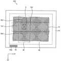
도 1은 본 발명의 일 실시예에 따른 센싱 표시 패널에 평면도이다.
도 2는 도 1의 A 부분에 대한 확대도이다.
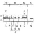
도 3은 도 2의 I-I'선을 따라 절단한 단면도이다.
도 4는 도 2의 II-II'선을 따라 절단한 단면도이다.
도 5a 내지 도 5e는 도 4에 도시된 센서 기판의 제조 방법을 설명하기 위한 단면도들이다.
도 6은 본 발명의 다른 실시예에 따른 센싱 표시 패널의 단면도이다.
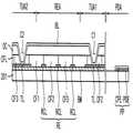
도 7은 도 6의 III-III'선을 따라 절단한 단면도이다.
도 8a 내지 도 8e는 도 7에 도시된 센서 기판의 제조 방법을 설명하기 위한 단면도들이다.
도 9는 본 발명의 다른 실시예에 따른 센싱 표시 패널의 단면도이다.
도 10은 본 발명의 다른 실시예에 따른 센싱 표시 패널의 단면도이다.
도 11a 내지 도 11e는 도 10에 도시된 센서 기판의 제조 방법을 설명하기 위한 단면도들이다.
도 12는 본 발명의 다른 실시예에 따른 센싱 표시 패널의 단면도이다.
도 13a 내지 도 13d는 도 12에 도시된 센서 기판의 제조 방법을 설명하기 위한 단면도들이다.
도 14a 내지 도 14d는 도 12에 도시된 센서 기판의 제조 방법을 설명하기 위한 평면도들이다.1 is a plan view of a sensing display panel according to an embodiment of the present invention.
2 is an enlarged view of a portion A in Fig.
3 is a cross-sectional view taken along the line I-I 'in FIG.
4 is a cross-sectional view taken along line II-II 'of FIG.
5A to 5E are cross-sectional views illustrating a method of manufacturing the sensor substrate shown in FIG.
6 is a cross-sectional view of a sensing display panel according to another embodiment of the present invention.
7 is a cross-sectional view taken along line III-III 'of FIG.
8A to 8E are cross-sectional views illustrating a method of manufacturing the sensor substrate shown in FIG.
9 is a cross-sectional view of a sensing display panel according to another embodiment of the present invention.
10 is a cross-sectional view of a sensing display panel according to another embodiment of the present invention.
11A to 11E are cross-sectional views for explaining a method of manufacturing the sensor substrate shown in FIG.
12 is a cross-sectional view of a sensing display panel according to another embodiment of the present invention.
13A to 13D are cross-sectional views illustrating a method of manufacturing the sensor substrate shown in FIG.
FIGS. 14A to 14D are plan views for explaining a method of manufacturing the sensor substrate shown in FIG.
이하, 도면들을 참조하여 본 발명의 바람직한 실시예들을 보다 상세하게 설명하기로 한다.Hereinafter, preferred embodiments of the present invention will be described in more detail with reference to the drawings.
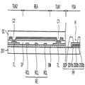
도 1은 본 발명의 일 실시예에 따른 센싱 표시 패널에 평면도이다. 도 2는 도 1의 A 부분에 대한 확대도이다. 도 3은 도 2의 I-I'선을 따라 절단한 단면도이다. 도 4는 도 2의 II-II'선을 따라 절단한 단면도이다.1 is a plan view of a sensing display panel according to an embodiment of the present invention. 2 is an enlarged view of a portion A in Fig. 3 is a cross-sectional view taken along the line I-I 'in FIG. 4 is a cross-sectional view taken along line II-II 'of FIG.
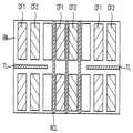
도 1 내지 도 4를 참조하면, 상기 센싱 표시 패널(500)은 액티브 영역(AA) 및 상기 액티브 영역(AA)을 둘러싸는 주변 영역(PA)을 포함하고, 표시 기판(100), 센서 기판(200), 액정층(300) 및 컬럼 스페이서(400)를 포함한다. 상기 액티브 영역(AA)은 터치가 센싱되고 영상이 표시되는 영역이고, 상기 주변 영역(PA)은 상기 터치 센싱 및 영상 표시를 위한 구동 회로 등이 실장될 수 있다.1 to 4, the
상기 표시 기판(100)은 제1 베이스 기판(101)을 포함하고, 상기 제1 베이스 기판(101)의 상기 액티브 영역(AA)에 배치된 복수의 게이트 라인들(GL), 복수의 공통 라인들(VL), 복수의 데이터 라인들(DL), 복수의 스위칭 소자들(TR), 복수의 화소 전극들(PE) 및 공통 전극(CE)을 포함한다.The
상기 게이트 배선(GL)은 제1 방향(D1)으로 연장되고 상기 제1 방향(D1)과 교차하는 제2 방향(D2)으로 배열된다. 상기 공통 라인(VL)은 상기 게이트 라인(GL)과 인접하고 평행하게 배열된다. 상기 데이터 라인(DL)은 상기 제2 방향(D2)으로 연장되고 상기 제1 방향(D1)으로 배열된다. 상기 스위칭 소자(TR)는 상기 게이트 라인(GL)에 연결된 게이트 전극(GE), 상기 데이터 라인(DL)에 연결된 소스 전극(SE) 및 상기 화소 전극(PE)에 연결된 드레인 전극(DE)을 포함한다.The gate lines GL are arranged in a second direction D2 extending in the first direction D1 and intersecting the first direction D1. The common line VL is arranged adjacent to and parallel to the gate line GL. The data lines DL extend in the second direction D2 and are arranged in the first direction D1. The switching device TR includes a gate electrode GE connected to the gate line GL, a source electrode SE connected to the data line DL and a drain electrode DE connected to the pixel electrode PE. do.
상기 화소 전극(PE)은 투명 도전층으로 형성되고, 상기 제1 베이스 기판(101)의 화소 영역(P)에 배치된다. 상기 공통 전극(CE)은 투명 도전층으로 형성되고, 상기 공통 라인(VL)과 콘택홀을 통해 전기적으로 연결되고 적어도 하나의 화소 영역(P)에 배치된 상기 화소 전극과 중첩된다. 상기 공통 전극(CE)은 복수의 슬릿 패턴이 형성될 수 있다.The pixel electrode PE is formed of a transparent conductive layer and is disposed in the pixel region P of the
도시된 바와 같이, 상기 표시 기판(100)은 게이트 절연층(110) 및 보호층(120)을 더 포함한다. 상기 게이트 절연층(110)은 상기 게이트 전극(GE), 상기 게이트 라인(GL) 및 상기 공통 라인(VL)을 포함하는 게이트 패턴을 덮는다. 상기 보호층(120)은 상기 데이터 라인(DL), 상기 소스 전극(SE) 및 상기 드레인 전극(DE)을 포함하는 소스 패턴을 덮는다.As shown in the figure, the
상기 센서 기판(200)은 제2 베이스 기판(201)을 포함하고, 상기 제2 베이스 기판(201)의 상기 액티브 영역(AA)에 배치된 차광 패턴(BM), 복수의 제1 전극들(TE), 복수의 제2 전극들(RE), 컬러 필터층(CFL) 및 오버 코팅층(OC)을 포함하고, 상기 주변 영역(PA)내에 포함된 패드 영역(PDA)에 배치된 복수의 패드들(PP)을 포함한다. 이하에서는 상기 제1 전극들(TE)은 구동 전극들로 명칭하고, 상기 제2 전극들(RE)은 센싱 전극들로 명칭한다.The
상기 차광 패턴(BM)은 상기 제2 베이스 기판(201) 상에 배치되어 광을 투과하는 투과 영역과 광을 차단하는 차단 영역을 정의하며, 상기 투과 영역은 상기 화소 영역(P)에 대응한다. The light blocking pattern BM defines a transmissive region that is disposed on the
상기 복수의 구동 전극들(TE)은 상기 제1 방향(D1)으로 연장되고, 상기 제2 방향(D2)으로 배열된다. 상기 구동 전극들(TE)은 정전식 터치 방식에 따라서 순차적으로 구동 신호를 전달한다. 각 구동 전극(TE)은 상기 제1 방향(D1)으로 배열된 복수의 구동 단위부들(TU1, TU2) 및 상기 제1 방향(D1)으로 인접한 상기 구동 단위부들(TU1, TU2)을 서로 연결하는 복수의 브릿지 라인들(BL)을 포함한다. 상기 구동 단위부(TU1, TU2)는 마름모 형상을 가지고, 그물 구조로 배열된 복수의 구동 라인들(TL)을 포함한다. 각 구동 라인(TL)은 상기 차광 패턴(BM)이 배치된 영역 내에 배치된다. 상기 브릿지 라인(BL)은 상기 구동 라인(TL)과 다른 금속층에 의해 패터닝되고, 단일 층 구조를 갖는다.The plurality of driving electrodes TE extend in the first direction D1 and are arranged in the second direction D2. The driving electrodes TE sequentially transmit driving signals according to the electrostatic touch method. Each drive electrode TE is connected to a plurality of drive unit units TU1 and TU2 arranged in the first direction D1 and to the drive unit units TU1 and TU2 adjacent to each other in the first direction D1 And includes a plurality of bridge lines (BL). The driving unit units TU1 and TU2 have a rhombic shape and include a plurality of driving lines TL arranged in a net structure. Each driving line TL is disposed in a region where the light-shielding pattern BM is disposed. The bridge line (BL) is patterned by a metal layer different from the driving line (TL), and has a single layer structure.
상기 구동 단위부들(TU1, TU2) 각각은 마름모 형상으로 한정하지 않으며, 터치 감도를 향상시키기 위한 다양한 형상을 설계될 수 있다.Each of the drive unit units TU1 and TU2 is not limited to a rhombus shape, and various shapes may be designed to improve touch sensitivity.
상기 복수의 센싱 전극들(RE)은 상기 제2 방향(D2)으로 연장되고, 상기 제1 방향(D1)으로 배열되고, 상기 센싱 전극들(TE)은 정전식 터치 방식에 따라서 터치에 대응하는 센싱 신호를 전달한다.The plurality of sensing electrodes RE extend in the second direction D2 and are arranged in the first direction D1 and the sensing electrodes TE are arranged in a first direction D1, And transmits a sensing signal.
각 센싱 전극(RE)은 상기 제2 방향(D2)으로 배열된 복수의 센싱 단위부들(RU1, RU2)을 포함하고, 상기 제2 방향(D2)으로 인접한 상기 센싱 단위부들(RU1, RU2)을 연결하는 센싱 연결 라인(RCL)을 포함한다. 상기 센싱 단위부들(RU1, RU2) 각각은 마름모 형상을 가지고, 그물 구조로 배열된 복수의 센싱 라인들(RL)을 포함한다. 상기 센싱 라인(RL)은 상기 차광 패턴(BM)이 배치된 영역 내에 배치된다. 상기 센싱 연결 라인(RCL)은 상기 센서 라인(RL)이 상기 제2 방향(D2)으로 연장된 것으로 상기 센싱 라인(RL)과 동일한 금속층에 의해 패터닝된다.Each of the sensing electrodes RE includes a plurality of sensing unit units RU1 and RU2 arranged in the second direction D2 and a plurality of sensing unit units RU1 and RU2 adjacent to each other in the second direction D2. And a sensing connection line (RCL) for connection. Each of the sensing unit units RU1 and RU2 has a rhombic shape and includes a plurality of sensing lines RL arranged in a net structure. The sensing line RL is disposed in a region where the light blocking pattern BM is disposed. The sensing connection line RCL extends in the second direction D2 and is patterned by the same metal layer as the sensing line RL.
상기 센싱 단위부들(RU1, RU2) 각각은 마름모 형상으로 한정하지 않으며, 터치 감도를 향상시키기 위한 다양한 형상으로 설계될 수 있다.Each of the sensing unit units RU1 and RU2 is not limited to a rhombus shape and may be designed in various shapes to improve touch sensitivity.
상기 컬러 필터층(CFL)은 제1 컬러, 제2 컬러 및 제3 컬러 패턴들(CF1, CF2, CF3)을 포함한다. 상기 제1 컬러, 제2 컬러 및 제3 컬러 패턴들(CF1, CF2, CF3) 각각은 상기 제2 방향(D2)으로 연장되고, 상기 제1 방향(D1)으로 배열된다. 상기 제1 컬러, 제2 컬러 및 제3 컬러 패턴들(CF1, CF2, CF3)은 레드, 그린 및 블루 패턴들 일 수 있으며, 이에 한정하지 않는다.The color filter layer CFL includes first color, second color and third color patterns CF1, CF2 and CF3. Each of the first color, the second color and the third color patterns CF1, CF2 and CF3 extends in the second direction D2 and is arranged in the first direction D1. The first color, the second color and the third color patterns CF1, CF2, and CF3 may be red, green, and blue patterns, but are not limited thereto.
상기 오버 코팅층(OC)은 상기 컬러 필터층(CFL) 위에 배치되어 상기 컬러 필터층(CFL)에 의해 울퉁불퉁해진 기판 표면을 평탄하게 한다.The overcoat layer OC is disposed on the color filter layer CFL to flatten the surface of the substrate which is rugged by the color filter layer CFL.
상기 브릿지 라인(BL)은 상기 컬러 필터층(CFL) 및 상기 오버 코팅층(OC)에 형성된 제1 및 제2 콘택홀들(C1, C2)을 통해 상기 제1 방향(D1)으로 인접한 상기 구동 단위부들(TU)을 서로 연결한다. 상기 브릿지 라인(BL)은 투명 도전층을 형성된다. 상기 투명 도전층은 도전성 산화물질로 형성되고, 상기 도전성 산화물질은 인듐 틴 옥사이드(ITO), 인듐 징크 옥사이드(IZO), 비정질 인듐 틴 옥사이드(a-ITO) 등을 포함할 수 있다.The bridge line BL is electrically connected to the driving unit units adjacent in the first direction D1 through the first and second contact holes C1 and C2 formed in the color filter layer CFL and the overcoat layer OC. (TU). The bridge line (BL) forms a transparent conductive layer. The transparent conductive layer may be formed of a conductive oxide material, and the conductive oxide material may include indium tin oxide (ITO), indium zinc oxide (IZO), amorphous indium tin oxide (a-ITO), and the like.
본 실시예에서는 상기 브릿지 라인(BL)이 상기 구동 단위부들(TU1, TU2)을 연결하는 것을 예로 하였으나, 상기 센싱 단위부들(RU1, RU2)을 연결할 수 있다. 즉, 상기 구동 라인(TL)이 상기 제1 방향(D1)으로 연장된 구동 연결 라인을 통해 서로 연결되고, 상기 센싱 단위부들(RU1, RU2)과 다른 층으로 형성된 브릿지 라인(BL)을 통해 서로 연결될 수 있다.Although the bridge line BL connects the driving unit units TU1 and TU2 in this embodiment, the sensing unit units RU1 and RU2 may be connected. That is, the driving lines TL are connected to each other through a driving connection line extending in the first direction D1, and the sensing unit units RU1 and RU2 are connected to each other through a bridge line BL formed of a different layer from the sensing unit units RU1 and RU2. Can be connected.
상기 패드(PP)는 패드 전극(PDE) 및 캡핑 전극(CPE)을 포함한다. 상기 패드 전극(PDE)은 상기 구동 전극(TE) 및 상기 센싱 전극(RE)과 동일한 금속층으로부터 형성되고, 상기 캡핑 전극(CPE)은 상기 브릿지 라인(BL)과 동일한 투명 도전층으로부터 형성된다. 상기 투명 도전층이 인듐 틴 옥사이드(ITO), 인듐 징크 옥사이드(IZO), 비정질 인듐 틴 옥사이드(a-ITO) 등과 같은 도전성 산화물질로 형성됨으로써 상기 패드 전극(PDE)이 산화되는 것을 막을 수 있다. 이에 터치 센싱의 구동 신뢰성을 개선할 수 있다.The pad PP includes a pad electrode PDE and a capping electrode CPE. The pad electrode PDE is formed of the same metal layer as the driving electrode TE and the sensing electrode RE and the capping electrode CPE is formed of the same transparent conductive layer as the bridge line BL. The transparent conductive layer may be formed of a conductive oxide material such as indium tin oxide (ITO), indium zinc oxide (IZO), amorphous indium tin oxide (a-ITO) or the like to prevent the pad electrode (PDE) from being oxidized. Accordingly, driving reliability of the touch sensing can be improved.
상기 액정층(300)은 상기 표시 기판(100) 및 상기 센서 기판(200) 사이에 배치된다. 상기 액정층(300)은 액정 분자를 포함하고, 상기 액정 분자는 상기 표시 기판(100)의 상기 회소 전극(PE) 및 상기 공통 전극(CE)의 전위차에 따라서 배열각이 변화된다. 상기 액정 분자의 배열각 변화에 따라서 상기 센싱 표시 패널(500)은 다양한 계조를 표시할 수 있다.The
상기 컬럼 스페이서(400)는 상기 표시 기판(100)과 상기 센서 기판(200)의 사이의 갭(Gap)을 유지시킨다. 상기 컬럼 스페이서(400)는 상기 표시 기판(100) 및 상기 센서 기판(200) 중 하나에 포함될 수 있다.The
도 5a 내지 도 5e는 도 4에 도시된 센서 기판의 제조 방법을 설명하기 위한 단면도들이다.5A to 5E are cross-sectional views illustrating a method of manufacturing the sensor substrate shown in FIG.
도 1, 도 2 및 도 5a를 참조하면, 베이스 기판(201) 위에 차광층을 형성한다. 상기 차광층을 패터닝하여 차광 패턴(BM)으로 패터닝한다. 상기 차광 패턴(BM)은 상기 베이스 기판(201)의 액티브 영역(AA)에 형성되고, 상기 차광 패턴(BM)이 형성된 영역을 차광 영역으로 정의되고 상기 차광 패턴(BM)이 형성되지 않은 영역은 투과 영역으로 정의된다. 상기 투과 영역은 상기 화소 전극(PE)이 형성된 상기 화소 영역(P)에 대응할 수 있다.Referring to FIGS. 1, 2 and 5A, a light shielding layer is formed on a
도 1, 도 2 및 도 5b를 참조하면, 상기 차광 패턴(BM)이 형성된 상기 베이스기판(201) 위에 금속층을 형성한다. 상기 금속층은 예를 들면, 크롬, 알루미늄, 탄탈륨, 몰리브덴, 티타늄, 텅스텐, 구리, 은 등의 금속 또는 이들의 합금 등으로 형성될 수 있다. 상기 금속층을 패터닝하여 상기 액티브 영역(AA)에 상기 구동 라인(TL), 상기 센싱 라인(RL) 및 상기 센싱 연결 라인(RCL)을 형성하고, 상기 주변 영역(PA)에 패드 전극(PDE)을 형성한다.1, 2 and 5B, a metal layer is formed on the
상기 구동 라인들(TL)은 상기 차광 패턴(BM)이 형성된 영역 내에 형성되고, 그물 구조로 연결되어 상기 구동 단위부들(TU1, TU2)를 형성한다. 상기 구동 단위부 들(TU1, TU2) 각각은 상기 제1 및 제2 방향들(D1, D2)에 배치된 다른 구동 단위부들과 서로 이격된다. 도시된 바와 같이, 제1 구동 단위 영역(TUA1)에는 제1 구동 단위부(TU1)의 구동 라인들(TL)이 형성되고, 상기 제1 구동 단위 영역(TUA1)으로부터 상기 제1 방향(D1)으로 이격된 제2 구동 단위 영역(TUA2)에는 제2 구동 단위부(TU2)의 구동 라인들(TL)이 형성된다.The driving lines TL are formed in a region where the light shielding pattern BM is formed and are connected by a net structure to form the driving unit units TU1 and TU2. Each of the drive unit units TU1 and TU2 is spaced apart from the other drive units disposed in the first and second directions D1 and D2. The driving lines TL of the first driving unit TU1 are formed in the first driving unit area TUA1 and the driving lines TL of the first driving unit TUA1 are formed in the first driving unit unit TUA1, The driving lines TL of the second driving unit TU2 are formed in the second driving unit area TUA2 spaced from the second driving unit TUA2.
상기 센싱 라인들(RL)은 상기 차광 패턴(BM)이 형성된 영역 내에 형성되고, 그물 구조의 상기 센싱 단위부들(RU1, RU2)를 형성한다. 상기 센싱 단위부들(RU1, RU2) 각각은 상기 제2 방향(D2)으로 인접한 다른 센싱 단위부(RU)와 상기 센싱 연결 라인(RCL)을 통해 서로 연결되고, 상기 제1 방향(D1)으로 인접한 다른 센싱 단위부(RU)와 이격된다. 도시된 바와 같이, 상기 제1 및 제2 구동 단위 영역들(TUA1, TUA2) 사이의 센싱 전극 영역(REA)에는 상기 제2 방향(D2)으로 배열된 제1 센싱 단위부(RU1)와 제2 센싱 단위부(RU2)를 연결하는 상기 센싱 연결 라인(RCL)이 형성된다.The sensing lines RL are formed in the region where the light-shielding pattern BM is formed, and form the sensing unit units RU1 and RU2 of the net structure. The sensing unit units RU1 and RU2 are connected to each other through the sensing connection unit RCL and the sensing unit RU adjacent to each other in the second direction D2 and are adjacent to each other in the first direction D1. And is separated from the other sensing unit unit (RU). As shown in the figure, a sensing electrode region REA between the first and second driving unit regions TUA1 and TUA2 includes a first sensing unit RU1 arranged in the second direction D2, The sensing connection line RCL connecting the sensing unit RU2 is formed.
상기 패드 전극(PDE)은 상기 패드 영역(PDA)에 형성된다.The pad electrode PDE is formed in the pad region PDA.
도 1, 도 2 및 도 5c를 참조하면, 상기 구동 라인(TL), 상기 센싱 라인(RL), 상기 센싱 연결 라인(RCL) 및 상기 패드 전극(PDE)이 형성된 상기 베이스 기판(201) 위에 컬러 필터층(CFL)을 형성한다. 상기 컬러 필터층(CFL)에는 제1 및 제2 콘택홀들(C1, C2)이 형성된다. 상기 제1 콘택홀(C1)은 상기 제1 구동 단위부(TU1)의 상기 구동 라인(TL)을 노출하고, 상기 제2 콘택홀(C2)은 상기 제2 구동 단위부(TU2)의 상기 구동 라인(TL)을 노출한다.Referring to FIGS. 1, 2 and 5C, on the
예를 들면, 제1 컬러 포토 레지스트층을 상기 베이스 기판(201) 위에 형성하고, 제1 컬러 마스크를 이용하여 상기 제2 방향(D2)으로 연장된 제1 컬러 패턴(CF1)을 형성한다. 이어, 제2 컬러 포토 레지스트층을 상기 제1 컬러 패턴(CF1)이 형성된 상기 베이스 기판(201) 위에 형성하고, 제2 컬러 마스크를 이용하여 상기 제1 컬러 패턴(CF1)과 평행한 제2 컬러 패턴(CF2)을 형성한다. 이어, 제3 컬러 포토 레지스트층을 상기 제1 및 제2 컬러 패턴들(CF1, CF2)이 형성된 상기 베이스 기판(201) 위에 형성하고 제3 컬러 마스크를 이용하여 상기 제2 컬러 패턴(CF2)과 평행한 제3 컬러 패턴(CF3)을 형성한다. 이때, 상기 제2 컬러 마스크는 상기 제1 콘택홀(C1)을 형성하기 위한 마스크 패턴을 포함하고, 또한, 상기 제3 컬러 패턴(CF3)을 패터닝하는 제3 컬러 마스크는 상기 제2 콘택홀(C2)을 형성하기 위한 마스크 패턴을 포함한다. 상기 제1 및 제2 콘택홀들(C1, C2)의 위치에 따라서 상기 마스크 패턴은 상기 제1, 제2 및 제3 컬러 마스크들 중 적어도 하나에 형성될 수 있다.For example, a first color photoresist layer is formed on the
이와 같이, 상기 컬러 마스크를 이용하여 상기 컬러 필터층(CFL)에 상기 콘택홀들(C1, C2)을 형성할 수 있다.In this manner, the contact holes C1 and C2 can be formed in the color filter layer CFL using the color mask.
도 1, 도 2 및 도 5d를 참조하면, 상기 컬러 필터층(CFL)이 형성된 베이스 기판(201) 위에 오버 코팅층(OC)을 형성한다.1, 2 and 5D, an overcoat layer OC is formed on a
상기 오버 코팅층(OC)은 상기 제1 및 제2 콘택홀들(C1, C2) 각각에 대응하여 홀들이 형성된다. 상기 오버 코팅층(OC)은 상기 패드 전극(PDE)이 형성된 상기 패드 영역(PDA)에는 형성되지 않는다. 이에 따라서, 상기 패드 전극(PDE)은 외부에 노출된다.The overcoat layer OC is formed with holes corresponding to the first and second contact holes C1 and C2, respectively. The overcoat layer OC is not formed in the pad region PDA on which the pad electrode PDE is formed. Accordingly, the pad electrode PDE is exposed to the outside.
도 1, 도 2 및 도 5e를 참조하면, 상기 오버 코팅층(OC) 위에 투명 도전층을 형성한다. 상기 투명 도전층은 투명 도전 산화물질로 형성되고, 상기 투명 도전 산화물질은 인듐 틴 옥사이드(ITO), 인듐 징크 옥사이드(IZO), 비정질 인듐 틴 옥사이드(a-ITO) 등을 포함할 수 있다. 상기 투명 도전층을 패터닝하여 상기 액티브 영역(AA)에 상기 브릿지 라인(BL)을 형성하고, 상기 패드 영역(PDA)에 캡핑 전극(CPE)을 형성한다.1, 2 and 5E, a transparent conductive layer is formed on the overcoat layer OC. The transparent conductive layer may be formed of a transparent conductive oxide material, and the transparent conductive oxide material may include indium tin oxide (ITO), indium zinc oxide (IZO), amorphous indium tin oxide (a-ITO), and the like. The transparent conductive layer is patterned to form the bridge line BL in the active area AA and a capping electrode CPE is formed in the pad area PDA.
상기 브릿지 라인(BL)은 상기 제1 및 제2 콘택홀들(C1, C2)을 통해 노출된 상기 제1 구동 단위부(TU1)의 상기 구동 라인(TL)과 상기 제2 구동 단위부(TU2)의 상기 구동 라인(TL)을 연결하고, 상기 오버 코팅층(OC) 위에 형성된다. 상기 캡핑 전극(CPE)은 상기 패드 전극(PDE)의 상부 및 측부를 덮도록 형성된다.The bridge line BL is connected to the drive line TL of the first drive unit TU1 exposed through the first and second contact holes C1 and C2 and the second drive unit TU2 ), And is formed on the overcoat layer (OC). The capping electrode CPE is formed to cover the upper and side portions of the pad electrode PDE.
도 4에 도시된 바와 같이, 상기 센서 기판(200)은 상기 브릿지 라인(BL)이 형성된 상기 베이스 기판(201) 위에 유기막으로 형성된 컬럼 스페이서(400)을 더 포함할 수 있다.As shown in FIG. 4, the
본 실시예에 따르면, 상기 브릿지 라인(BL)이 상기 액정층(300)과 직접 접촉된다. 이에 따라서, 상기 액정층(300)의 비정상상 구동에 의해 텍스쳐(Texture)가 발생될 수 있다. 이러한 문제점을 해결하기 위해서, 본 실시예에 따르면 상기 브릿지 라인(BL)이 형성되는 영역의 상기 차광 패턴(BM)은 폭을 충분히 확장시켜 상기 텍스쳐에 의한 표시 불량을 막을 수 있다.According to this embodiment, the bridge line (BL) is in direct contact with the liquid crystal layer (300). Accordingly, a texture may be generated by the abnormal driving of the
본 실시예에 따르면, 투명 도전 산화물질로 형성된 상기 캡핑 전극(CPE)에 의해 상기 패드 전극(PDE)을 캡핑함으로써 상기 패드 전극(PDE)이 산화되는 것을 막아 구동 신뢰성을 향상시킬 수 있다.According to this embodiment, the capping electrode CPE formed of a transparent conductive oxide material prevents the pad electrode PDE from being oxidized by capping the pad electrode PDE, thereby improving driving reliability.
본 실시예에 따르면, 상기 컬러 필터층 및 상기 오버 코팅층을 형성하는 마스크의 변형을 통해서 상기 콘택홀을 형성할 수 있다. 이에 따라서, 상기 콘택홀 형성을 위한 마스크 공정을 생략할 수 있다.According to the present embodiment, the contact hole can be formed through deformation of the mask for forming the color filter layer and the overcoat layer. Accordingly, the mask process for forming the contact holes can be omitted.
이하에서는 이전 실시예와 동일한 구성 요소는 동일한 도면 부호를 부여하고 반복되는 설명은 생략 또는 간략하게 한다.Hereinafter, the same components as those of the previous embodiment will be denoted by the same reference numerals, and repeated descriptions will be omitted or simplified.
도 6은 본 발명의 다른 실시예에 따른 센싱 표시 패널의 평면도이다. 도 7은 도 6의 III-III'선을 따라 절단한 단면도이다.6 is a plan view of a sensing display panel according to another embodiment of the present invention. 7 is a cross-sectional view taken along line III-III 'of FIG.
도 1, 도 6 및 도 7을 참조하면, 상기 센싱 표시 패널(510)은 액티브 영역(AA) 및 상기 액티브 영역(AA)을 둘러싸는 주변 영역(PA)을 포함하고, 표시 기판(100), 센서 기판(200), 액정층(300) 및 컬럼 스페이서(400)를 포함한다.1, 6 and 7, the
상기 표시 기판(100)은 이전 실시예와 실질적으로 동일하므로 반복되는 설명은 생략한다.Since the
상기 센서 기판(200)은 제2 베이스 기판(201)을 포함하고, 상기 제2 베이스 기판(201)의 상기 액티브 영역(AA)에 배치된 차광 패턴(BM), 복수의 구동 전극들(TE), 절연층(205), 복수의 센싱 전극들(RE), 컬러 필터층(CFL) 및 오버 코팅층(OC)을 포함하고, 상기 주변 영역(PA)내에 포함된 패드 영역(PDA)에 배치된 복수의 패드들(PP)을 포함한다. 본 실시예의 상기 센서 기판(200)은 도 4에 도시된 이전 실시예의 센서 기판과 비교하여 브릿지 라인(BL)을 생략할 수 있다.The
상기 차광 패턴(BM)은 상기 제2 베이스 기판(201) 상에 배치되어 광을 투과하는 투과 영역과 광을 차단하는 차단 영역을 정의하며, 상기 투과 영역은 상기 화소 영역(P)에 대응한다.The light blocking pattern BM defines a transmissive region that is disposed on the
본 실시예의 상기 구동 전극들(TE)은 상기 제1 방향(D1)으로 연장되고, 상기 제2 방향(D2)으로 배열된다. 상기 구동 전극(TE)은 상기 제1 방향(D1)으로 배열된 복수의 구동 단위부들(TU1, TU2) 및 상기 제1 방향(D1)으로 인접한 상기 구동 단위부들(TU1, TU2)을 서로 연결하는 구동 연결 라인(TCL)을 포함한다. 상기 구동 단위부들(TU1, TU2) 각각은 그물 구조로 연결된 복수의 구동 라인들(TL)을 포함한다. 상기 구동 연결 라인(TCL)은 상기 구동 라인(TL)으로부터 연장되어 형성된다.The driving electrodes TE of the present embodiment extend in the first direction D1 and are arranged in the second direction D2. The driving electrode TE connects the plurality of driving unit units TU1 and TU2 arranged in the first direction D1 and the driving unit units TU1 and TU2 adjacent to each other in the first direction D1 And a driving connection line (TCL). Each of the driving unit units TU1 and TU2 includes a plurality of driving lines TL connected in a net structure. The driving connection line TCL is formed extending from the driving line TL.
상기 절연층(205)은 상기 구동 전극들(TE)을 커버하도록 상기 제2 베이스 기판(201) 위에 형성된다.The insulating
상기 센싱 전극들(RE)은 상기 제2 방향(D2)으로 연장되고, 상기 제1 방향(D1)으로 배열된다. 상기 센싱 전극(RE)은 상기 제2 방향(D2)으로 배열된 복수의 센싱 단위부들(RU) 및 상기 제2 방향(D2)으로 인접한 상기 센싱 단위부들(RU1, RU2)을 서로 연결하는 센싱 연결 라인(RCL)을 포함한다. 상기 센싱 단위부들(RU1, RU2) 각각은 그물 구조로 연결된 복수의 센싱 라인들(RL)을 포함한다. 상기 센싱 연결 라인(RCL)은 상기 센싱 라인(RL)으로부터 연장되어 형성된다.The sensing electrodes RE extend in the second direction D2 and are arranged in the first direction D1. The sensing electrode RE includes a sensing unit unit RU arranged in the second direction D2 and a sensing unit RU2 connecting the sensing unit units RU1 and RU2 adjacent to each other in the second direction D2. Line (RCL). Each of the sensing units RU1 and RU2 includes a plurality of sensing lines RL connected in a net structure. The sensing connection line RCL is formed extending from the sensing line RL.
본 실시예에 따르면, 상기 구동 전극들(TE)이 위치한 층과 상기 센싱 전극들(RE)이 위치한 층 사이에 상기 절연층(205)을 배치함으로써 상기 절연층(205)에 의해 상기 구동 전극들(TE) 및 상기 센서 전극들(RE)이 서로 전기적으로 절연될 수 있다. 따라서, 도 4에 설명된 이전 실시예의 상기 브릿지 라인(BL)이 생략될 수 있다.The insulating
상기 컬러 필터층(CFL)은 제1, 제2 및 제3 컬러 패턴들(CF1, CF2, CF3)을 포함한다. 상기 제1, 제2 및 제3 컬러 패턴들(CF1, CF2, CF3)은 상기 제2 방향(D2)으로 연장되고, 상기 제1 방향(D1)으로 배열된다. The color filter layer CFL includes first, second and third color patterns CF1, CF2 and CF3. The first, second and third color patterns CF1, CF2 and CF3 extend in the second direction D2 and are arranged in the first direction D1.
상기 오버 코팅층(OC)은 상기 컬러 필터층(CFL) 위에 배치되어 상기 컬러 필터층(CFL)에 의해 울퉁불퉁해진 표면을 평탄하게 한다.The overcoat layer (OC) is disposed on the color filter layer (CFL) to flatten the rugged surface by the color filter layer (CFL).
본 실시예의 상기 패드(PP)는 패드 전극(PDE)과 오버 코팅 패턴(OCP)을 포함하고, 상기 패드 전극(PDE)과 오버 코팅 패턴(OCP) 사이에는 상기 절연층(205)이 배치된다. 상기 패드 전극(PDE)은 상기 구동 라인(TL)과 동일한 금속층으로부터 형성된다. 상기 오버 코팅 패턴(OCP)은 상기 패드 전극(PDE)의 상부 일부분을 노출하는 홀(H)을 포함하고 상기 일부분을 제외한 상기 패드 전극(PDE)의 상부 및 측부를 커버한다. 상기 홀(H)에 의해 노출된 상기 패드 전극(PDE)은 구동 칩의 단자가 본딩된다.The pad PP of the present embodiment includes a pad electrode PDE and an overcoat pattern OCP and the insulating
본 실시예에 따르면, 상기 오버 코팅 패턴(OCP)에 의해 상기 패드 전극(PDE)은 외부 공기에 의해 부식되는 것을 막을 수 있다. 또한, 도 4에서 설명된 이전 실시예와 비교하여 상기 구동 단위부들을 서로 연결하는 구동 연결 라인을 금속으로 형성함으로써 배선 저항을 줄일 수 있다.According to the present embodiment, the overcoat pattern (OCP) can prevent the pad electrode (PDE) from being corroded by outside air. In addition, as compared with the previous embodiment shown in FIG. 4, the driving connection line connecting the driving unit parts to each other is formed of metal, thereby reducing the wiring resistance.
또한, 도시되지 않았으나, 상기 패드 전극(PDE)은 상기 센싱 전극(RE)과 동일한 금속층으로부터 형성될 수 있다. 이 경우, 상기 오버 코팅 패턴(OCP)은 상기 패드 전극(PDE)과 직접 접촉되어 배치될 수 있다.Also, though not shown, the pad electrode PDE may be formed of the same metal layer as the sensing electrode RE. In this case, the overcoat pattern (OCP) may be disposed in direct contact with the pad electrode (PDE).
도 8a 내지 도 8e는 도 7에 도시된 센서 기판의 제조 방법을 설명하기 위한 단면도들이다.8A to 8E are cross-sectional views illustrating a method of manufacturing the sensor substrate shown in FIG.
도 1, 도 7 및 도 8a를 참조하면, 베이스 기판(201) 위에 차광 물질을 형성한다. 마스크를 이용하여 상기 차광 물질을 차광 패턴(BM)으로 패터닝한다. 상기 차광 패턴(BM)은 상기 베이스 기판(201)의 액티브 영역(AA)에 형성되고, 상기 차광 패턴(BM)이 형성된 영역을 차광 영역으로 정의한다. 상기 차광 패턴(BM)에 의해 상기 화소 영역(P)에 대응하는 영역은 투과 영역으로 정의된다.Referring to FIGS. 1, 7, and 8A, a light shielding material is formed on a
도 1, 도 7 및 도 8b를 참조하면, 상기 차광 패턴(BM)이 형성된 상기 베이스기판(201) 위에 제1 금속층을 형성한다. 상기 제1 금속층은 예를 들면, 크롬, 알루미늄, 탄탈륨, 몰리브덴, 티타늄, 텅스텐, 구리, 은 등의 금속 또는 이들의 합금 등으로 형성될 수 있다. 상기 제1 금속층을 패터닝하여 상기 액티브 영역(AA)에 상기 구동 라인(TL) 및 상기 구동 연결 라인(TCL)을 형성하고, 상기 주변 영역(PA)에 패드 전극(PDE)을 형성한다.Referring to FIGS. 1, 7 and 8B, a first metal layer is formed on the
상기 구동 라인들(TL)은 상기 차광 패턴(BM)이 형성된 영역 내에 형성되고, 그물 구조로 연결되어 상기 구동 단위부들(TU1, TU2)를 형성한다. 상기 구동 단위부 들(TU1, TU2) 각각은 상기 제1 방향(D1)으로 인접한 다른 구동 단위부와 상기 구동 연결 라인(TCL)을 통해 서로 연결되고, 상기 제2 방향(D2)으로 인접한 다른 구동 단위부와 이격된다. 도시된 바와 같이, 제1 구동 단위 영역(TUA1)에는 제1 구동 단위부(TU1)의 구동 라인들(TL)이 형성되고, 상기 제1 구동 단위 영역(TUA1)으로부터 상기 제1 방향(D1)으로 이격된 제2 구동 단위 영역(TUA2)에는 제2 구동 단위부(TU2)의 구동 라인들(TL)이 형성된다. 상기 제1 및 제2 구동 단위 영역들(TUA1, TUA2) 사이의 센싱 전극 영역(REA)에는 상기 제1 방향(D1)으로 배열된 제1 구동 단위부(TU1)와 제2 구동 단위부(TU2)를 연결하는 상기 구동 연결 라인(TCL)이 형성된다.The driving lines TL are formed in a region where the light shielding pattern BM is formed and are connected by a net structure to form the driving unit units TU1 and TU2. Each of the driving unit units TU1 and TU2 is connected to another driving unit unit adjacent in the first direction D1 through the driving connection line TCL, And is separated from the unit portion. The driving lines TL of the first driving unit TU1 are formed in the first driving unit area TUA1 and the driving lines TL of the first driving unit TUA1 are formed in the first driving unit unit TUA1, The driving lines TL of the second driving unit TU2 are formed in the second driving unit area TUA2 spaced from the second driving unit TUA2. The first driving unit TU1 and the second driving unit TU2 arranged in the first direction D1 are arranged in the sensing electrode area REA between the first and second driving unit areas TUA1 and TUA2, The driving connection line TCL is formed.
상기 패드 전극(PDE)은 상기 패드 영역(PDA)에 형성된다.The pad electrode PDE is formed in the pad region PDA.
도 1, 도 7 및 도 8c를 참조하면, 상기 구동 라인(TL), 상기 구동 연결 라인(TCL) 및 상기 패드 전극(PDE)이 형성된 상기 베이스 기판(201) 위에 절연층(205)을 형성한다. 상기 절연층(205)은 질화 실리콘(SiNx) 또는 산화 실리콘(SiOx)으로 이루어질 수 있고, 플라즈마 화학 기상 증착(Plasma Enhanced Chemical Vapor Deposition, PECVD) 방법을 이용하여 형성할 수 있다. 또한, 상기 절연층(205)은 재질 및 형성 공정이 서로 다른 이중 층 구조로 형성할 수도 있다.Referring to FIGS. 1, 7 and 8C, an insulating
상기 절연층(205)이 형성된 상기 베이스 기판(201) 위에 제2 금속층을 형성한다. 상기 제2 금속층은 예를 들면, 크롬, 알루미늄, 탄탈륨, 몰리브덴, 티타늄, 텅스텐, 구리, 은 등의 금속 또는 이들의 합금 등으로 형성될 수 있다. 상기 제2 금속층을 패터닝하여 상기 액티브 영역(AA)에 상기 센싱 라인(RL) 및 상기 센싱 연결 라인(RCL)을 형성한다.A second metal layer is formed on the
상기 센싱 라인들(RL)은 상기 차광 패턴(BM)이 형성된 영역 내에 형성되고, 그물 구조로 연결되어 상기 센싱 단위부들(RU1, RU2)을 형성한다. 상기 센싱 단위부 들(RU1, RU2) 각각은 상기 제2 방향(D2)으로 인접한 다른 센싱 단위부와 상기 센싱 연결 라인(SCL)을 통해 서로 연결되고, 상기 제1 방향(D1)으로 인접한 다른 센싱 단위부와 이격된다. 도시된 바와 같이, 상기 제1 및 제2 구동 단위 영역들(TUA1, TUA2) 사이의 센싱 전극 영역(REA)에는 상기 제2 방향(D2)으로 배열된 제1 센싱 단위부(RU1)와 제2 센싱 단위부(RU2)를 연결하는 상기 센싱 연결 라인(RCL)이 형성된다.The sensing lines RL are formed in a region where the light shielding pattern BM is formed and are connected to each other by a net structure to form the sensing unit units RU1 and RU2. Each of the sensing unit units RU1 and RU2 is connected to another sensing unit unit adjacent in the second direction D2 through the sensing connection line SCL, And is separated from the unit portion. As shown in the figure, a sensing electrode region REA between the first and second driving unit regions TUA1 and TUA2 includes a first sensing unit RU1 arranged in the second direction D2, The sensing connection line RCL connecting the sensing unit RU2 is formed.
도 1, 도 7 및 도 8d를 참조하면, 상기 센싱 라인(RL) 및 상기 센싱 연결 라인(RCL)이 형성된 상기 베이스 기판(201) 위에 컬러 필터층(CFL)을 형성한다. 상기 컬러 필터층(CFL)은 상기 액티브 영역(AA)에 형성된다.Referring to FIGS. 1, 7 and 8D, a color filter layer (CFL) is formed on the
예를 들면, 제1 컬러 포토 레지스트층을 상기 베이스 기판(201) 위에 형성하고, 제1 컬러 마스크를 이용하여 상기 제2 방향(D2)으로 연장된 제1 컬러 패턴(CF1)을 형성한다. 이어, 제2 컬러 포토 레지스트층을 상기 제1 컬러 패턴(CF1)이 형성된 상기 베이스 기판(201) 위에 형성하고, 제2 컬러 마스크를 이용하여 상기 제1 컬러 패턴(CF1)과 평행한 제2 컬러 패턴(CF2)을 형성한다. 이어, 제3 컬러 포토 레지스트층을 상기 제1 및 제2 컬러 패턴들(CF1, CF2)이 형성된 상기 베이스 기판(201) 위에 형성하고 제3 컬러 마스크를 이용하여 상기 제2 컬러 패턴(CF2)과 평행한 제3 컬러 패턴(CF3)을 형성한다.For example, a first color photoresist layer is formed on the
도 1, 도 7 및 도 8e를 참조하면, 상기 컬러 필터층(CFL)이 형성된 상기 베이스 기판(201) 위에 오버 코팅층(OC)을 형성한다. 상기 오버 코팅층(OC)은 상기 패드 전극(PDE) 위에 형성된 오버 코팅 패턴(OCP)을 포함한다.Referring to FIGS. 1, 7 and 8E, an overcoat layer OC is formed on the
도시된 바와 같이, 상기 액티브 영역(AA)에 형성된 상기 컬러 필터층(CFL)의 울퉁불퉁한 표면은 상기 오버 코팅층(OC)에 의해 평탄화 된다. 상기 오버 코팅 패턴(OCP)은 상기 패드 전극(PDE)의 상부 일부분에 대응하여 홀(H)이 형성되고 상기 홀(H)이 형성된 영역을 제외한 상기 패드 전극(PDE)의 나머지 상부 및 측부를 덮도록 형성된다. 상기 홀(H)에 의해 상기 패드 전극(PDE) 위의 상기 절연층(205)이 노출된다.As shown, the rugged surface of the color filter layer (CFL) formed in the active area AA is planarized by the overcoat layer OC. The overcoat pattern OCP includes a hole H formed corresponding to an upper portion of the pad electrode PDE and covering the remaining upper and side portions of the pad electrode PDE except the region where the hole H is formed. . The hole H exposes the insulating
이후, 상기 오버 코팅층(OC)을 마스크로 하여 상기 오버 코팅 패턴(OCP)에 의해 노출된 상기 패드 전극(PDE) 위의 상기 절연층(205)을 제거하여 상기 패드 전극(PDE)을 노출시킨다. 결과적으로, 상기 패드(PP)는 상기 패드 전극(PDE)과 상기 오버 코팅 패턴(OCP)을 포함한다.Then, the insulating
본 실시예에 따르면, 상기 구동 전극(TE)과 상기 센싱 전극(RE) 사이에 상기 절연층(205)을 형성함으로써 콘택홀을 생략할 수 있다. 이에 따라서, 상기 콘택홀 형성을 위한 별도의 마스크 공정을 생략할 수 있다.According to the present embodiment, the insulating
또한, 상기 패드 전극(PDE)은 상기 오버 코팅 패턴(OCP)에 의해 공기에 포함된 수분으로부터 손상되는 것을 방지할 수 있다.In addition, the pad electrode (PDE) can be prevented from being damaged by the moisture contained in the air by the overcoat pattern (OCP).
도 9는 본 발명의 다른 실시예에 따른 센싱 표시 패널의 단면도이다.9 is a cross-sectional view of a sensing display panel according to another embodiment of the present invention.
도 9를 참조하면, 본 실시예에 따른 센싱 표시 패널(520)은 도 7에 도시된 이전 실시예에 따른 센싱 표시 패널(510)과 비교하여 상기 구동 전극(TE) 및 상기 패드 전극(PDE)을 이중 층 구조로 형성하는 것을 제외하고는 실질적으로 동일하다. 이에 반복되는 설명은 생략한다.9, the
본 실시예에 따른 상기 센싱 표시 패널(520)은 액티브 영역(AA) 및 상기 액티브 영역(AA)을 둘러싸는 주변 영역(PA)을 포함하고, 표시 기판(100), 센서 기판(200), 액정층(300) 및 컬럼 스페이서(400)를 포함한다.The
상기 센서 기판(200)은 제2 베이스 기판(201)을 포함하고, 상기 제2 베이스 기판(201)의 상기 액티브 영역(AA)에 배치된 차광 패턴(BM), 복수의 구동 전극들(TE), 절연층(205), 복수의 센싱 전극들(RE), 컬러 필터층(CFL) 및 오버 코팅층(OC)을 포함하고, 상기 주변 영역(PA)내에 포함된 패드 영역(PDA)에 배치된 복수의 패드들(PP)을 포함한다.The
본 실시예의 상기 구동 전극들(TE)은 상기 제1 방향(D1)으로 연장되고, 상기 제2 방향(D2)으로 배열된다. 각 구동 전극(TE)은 상기 제1 방향(D1)으로 배열된 복수의 구동 단위부들(TU1, TU2) 및 상기 제1 방향(D1)으로 인접한 상기 구동 단위부들(TU1, TU2)을 서로 연결하는 구동 연결 라인(TCL)을 포함한다. 상기 구동 단위부들(TU1, TU2) 각각은 그물 구조로 연결된 복수의 구동 라인들(TL)을 포함한다. 상기 구동 연결 라인(TCL)은 상기 구동 라인(TL)과 동일한 금속층으로부터 형성된다.The driving electrodes TE of the present embodiment extend in the first direction D1 and are arranged in the second direction D2. Each drive electrode TE is connected to a plurality of drive unit units TU1 and TU2 arranged in the first direction D1 and to the drive unit units TU1 and TU2 adjacent to each other in the first direction D1 And a driving connection line (TCL). Each of the driving unit units TU1 and TU2 includes a plurality of driving lines TL connected in a net structure. The driving connection line TCL is formed from the same metal layer as the driving line TL.
본 실시예에 따르면, 상기 구동 라인(TL) 및 상기 구동 연결 라인(TCL)은 이중 층 구조를 갖는다. 예를 들면, 상기 구동 라인(TL) 및 상기 구동 연결 라인(TCL) 각각은 금속층으로부터 형성된 금속 라인(221a) 및 투명 도전층으로부터 형성된 투명 라인(222a)을 포함한다. 상기 금속 라인(221a)은 크롬, 알루미늄, 탄탈륨, 몰리브덴, 티타늄, 텅스텐, 구리, 은 등의 금속 또는 이들의 합금 등으로 형성될 수 있다. 상기 투명 라인(222a)은 인듐 틴 옥사이드(ITO), 인듐 징크 옥사이드(IZO), 비정질 인듐 틴 옥사이드(a-ITO) 등으로 형성될 수 있다.According to the present embodiment, the driving line TL and the driving connection line TCL have a double-layer structure. For example, each of the driving line TL and the driving connection line TCL includes a
또한, 본 실시예의 상기 패드(PP)는 상기 금속층으로부터 형성된 패드 전극(221b), 투명 도전층으로 형성된 캡핑 전극(222b) 및 오버 코팅 패턴(OCP)을 포함한다.In addition, the pad PP of the present embodiment includes a
본 실시예에 따른 센서 기판(200)의 제조 방법은 도 8a 내지 도 8e를 참조하여 설명된 이전 실시예의 제조 방법과 비교하여, 상기 구동 라인(TL), 구동 연결 라인(TCL) 및 상기 패드(PP)가 금속층 및 투명 도전층을 포함하는 이중 층으로부터 형성되는 것을 제외하고 나머지 제조 공정은 실질적으로 동일하다.The manufacturing method of the
본 실시예는 도 7에 도시된 이전 실시예와 비교할 때, 상기 오버 코팅 패턴(OCP)뿐만 아니라, 상기 캡핑 전극(222b)이 상기 패드 전극(221b)을 캡핑함으로써 상기 패드 전극(221b)이 공기 중의 수분에 의해 손상되는 것을 막을 수 있어 구동 신뢰성을 향상시킬 수 있다.The present embodiment is different from the previous embodiment shown in FIG. 7 in that not only the overcoat pattern OCP but also the
도 10은 본 발명의 다른 실시예에 따른 센싱 표시 패널의 단면도이다.10 is a cross-sectional view of a sensing display panel according to another embodiment of the present invention.
도 1, 도 2 및 도 10을 참조하면, 상기 센싱 표시 패널(530)은 액티브 영역(AA) 및 상기 액티브 영역(AA)을 둘러싸는 주변 영역(PA)을 포함하고, 표시 기판(100), 센서 기판(200), 액정층(300) 및 컬럼 스페이서(400)를 포함한다.1, 2, and 10, the
상기 표시 기판(100)은 이전 실시예와 실질적으로 동일하므로 반복되는 설명은 생략한다.Since the
상기 센서 기판(200)은 제2 베이스 기판(201)을 포함하고, 상기 제2 베이스 기판(201)의 상기 액티브 영역(AA)에 배치된 차광 패턴(BM), 복수의 구동 전극들(TE), 복수의 센싱 전극들(RE), 컬러 필터층(CFL) 및 오버 코팅층(OC)을 포함하고, 상기 주변 영역(PA)내에 포함된 패드 영역(PDA)에 배치된 복수의 패드들(PP)을 포함한다. 본 실시예의 상기 센서 기판(200)은 도 4에 도시된 이전 실시예와 비교하여 브릿지 라인(BL) 위에 오버 코팅층(OC)이 배치되고, 상기 브릿지 라인(BL) 및 상기 패드(PP)의 구조가 서로 다르다.The
본 실시예의 상기 구동 전극들(TE)은 상기 제1 방향(D1)으로 연장되고, 상기 제2 방향(D2)으로 배열된다. 상기 구동 전극(TE)은 상기 제1 방향(D1)으로 배열된 복수의 구동 단위부들(TU) 및 상기 제1 방향(D1)으로 인접한 상기 구동 단위부들(TU1, TU2)을 서로 연결하는 복수의 브릿지 라인들(BL)을 포함한다. 상기 브릿지 라인(BL)은 상기 구동 라인(TL)과 다른 금속층으로부터 형성된다. 상기 브릿지 라인(BL)은 금속층으로부터 형성된 금속 라인(232a) 및 투명 도전층으로부터 형성된 투명 라인(233a)으로 이루어진 이중 층 구조를 갖는다.The driving electrodes TE of the present embodiment extend in the first direction D1 and are arranged in the second direction D2. The driving electrode TE includes a plurality of driving unit units TU arranged in the first direction D1 and a plurality of driving unit units TU1 and TU2 adjacent to each other in the first direction D1. And bridge lines BL. The bridge line BL is formed from a metal layer different from the driving line TL. The bridge line BL has a double layer structure composed of a
상기 센싱 전극들(RE)은 상기 제2 방향(D2)으로 연장되고, 상기 제1 방향(D1)으로 배열된다. 상기 센싱 전극(RE)은 상기 제2 방향(D2)으로 배열된 복수의 센싱 단위부들(RU1, RU2) 및 상기 제2 방향(D2)으로 인접한 상기 센싱 단위부들(RU RU1, RU2)을 서로 연결하는 센싱 연결 라인(RCL)을 포함한다. 상기 센싱 단위부들(RU1, RU2) 각각은 그물 구조로 연결된 복수의 센싱 라인들(RL)을 포함한다. 상기 센싱 연결 라인(RCL)은 상기 센싱 라인(RL)과 동일한 금속층으로부터 형성된다.The sensing electrodes RE extend in the second direction D2 and are arranged in the first direction D1. The sensing electrode RE may include a plurality of sensing unit units RU1 and RU2 arranged in the second direction D2 and a plurality of sensing unit units RU RU1 and RU2 adjacent to each other in the second direction D2, And a sensing connection line (RCL). Each of the sensing units RU1 and RU2 includes a plurality of sensing lines RL connected in a net structure. The sensing connection line RCL is formed from the same metal layer as the sensing line RL.
상기 컬러 필터층(CFL)은 제1, 제2 및 제3 컬러 패턴들(CF1, CF2, CF3)을 포함하고, 상기 제1, 제2 및 제3 컬러 패턴들(CF1, CF2, CF3)은 상기 제2 방향(D2)으로 연장되고 상기 제1 방향(D1)으로 배열된다. 상기 컬러 필터층(CFL)은 상기 제1 방향(D1)으로 인접한 상기 구동 단위들(TU1, TU2)의 구동 라인들(TL)을 노출하는 제1 및 제2 콘택홀들(C1, C2)을 포함한다. 상기 제1 및 제2 콘택홀들(C1, C2)을 통해 상기 브릿지 라인(BL)은 상기 구동 단위들(TU1, TU2)을 서로 연결한다.The color filter layer CFL includes first, second, and third color patterns CF1, CF2, and CF3, and the first, second, and third color patterns CF1, CF2, Extend in the second direction D2 and are arranged in the first direction D1. The color filter layer CFL includes first and second contact holes C1 and C2 exposing driving lines TL of the driving units TU1 and TU2 adjacent to each other in the first direction D1. do. The bridge line BL connects the driving units TU1 and TU2 through the first and second contact holes C1 and C2.
본 실시예의 상기 패드(PP)는 패드 전극(231b, 232b), 캡핑 전극(233b) 및 오버 코팅 패턴(OCP)을 포함한다. 상기 패드 전극은 상기 센싱 라인(RL)과 동일한 금속층으로부터 제1 금속 전극(231b)과 상기 브릿지 라인(BL)의 상기 금속 라인(232a)과 동일한 금속층으로부터 형성된 상기 제2 금속 전극(231b)을 포함한다. 상기 캡핑 전극(233b)은 상기 브릿지 라인(BL)의 상기 투명 라인(233a)과 동일한 도전층으로부터 형성된다.The pad PP of the present embodiment includes
본 실시예에 따르면, 상기 캡핑 전극(233b) 및 상기 오버 코팅 패턴(OCP)이 상기 패드 전극(231b, 232b)을 캡핑함으로써 상기 패드 전극(231b, 232b)이 공기 중의 수분에 의해 손상되는 것을 막을 수 있다. 또한, 상기 브릿지 라인(BL)이 금속 라인(232a)을 포함함으로써 배선 저항을 줄여 구동 신뢰성을 개선할 수 있다.According to the present embodiment, the capping
도 11a 내지 도 11e는 도 10에 도시된 센서 기판의 제조 방법을 설명하기 위한 단면도들이다.11A to 11E are cross-sectional views for explaining a method of manufacturing the sensor substrate shown in FIG.
도 2, 도 10 및 도 11a를 참조하면, 베이스 기판(201) 위에 차광층을 형성하고, 상기 차광층을 패터닝하여 차광 패턴(BM)을 형성한다.2, 10 and 11A, a light shielding layer is formed on a
도 2, 도 10 및 도 11b를 참조하면, 상기 차광 패턴(BM)이 형성된 상기 베이스 기판(201) 위에 금속층을 형성한다. 상기 금속층은 예를 들면, 크롬, 알루미늄, 탄탈륨, 몰리브덴, 티타늄, 텅스텐, 구리, 은 등의 금속 또는 이들의 합금 등으로 형성될 수 있다. 상기 금속층을 패터닝하여 상기 구동 라인(TL), 상기 센싱 라인(RL) 및 상기 센싱 연결 라인(RCL)을 형성하고, 상기 패드 전극의 제1 금속 전극(231b)을 형성한다.2, 10 and 11B, a metal layer is formed on the
도시된 바와 같이, 제1 구동 단위 영역(TUA1)에는 제1 구동 단위부(TU1)의 구동 라인들(TL)이 형성되고, 상기 제1 구동 단위 영역(TUA1)으로부터 상기 제1 방향(D1)으로 이격된 제2 구동 단위 영역(TUA2)에는 제2 구동 단위부(TU2)의 구동 라인들(TL)이 형성된다.The driving lines TL of the first driving unit TU1 are formed in the first driving unit area TUA1 and the driving lines TL of the first driving unit TUA1 are formed in the first driving unit unit TUA1, The driving lines TL of the second driving unit TU2 are formed in the second driving unit area TUA2 spaced from the second driving unit TUA2.
상기 센싱 라인들(RL)은 상기 차광 패턴(BM)이 형성된 영역 내에 형성되고, 그물 구조의 상기 센싱 단위부들(RU1, RU2)를 형성한다. 도시된 바와 같이, 상기 제1 및 제2 구동 단위 영역들(TUA1, TUA2) 사이의 센싱 전극 영역(REA)에는 상기 제2 방향(D2)으로 배열된 제1 센싱 단위부(RU1)와 제2 센싱 단위부(RU2)를 연결하는 상기 센싱 연결 라인(RCL)이 형성된다.The sensing lines RL are formed in the region where the light-shielding pattern BM is formed, and form the sensing unit units RU1 and RU2 of the net structure. As shown in the figure, a sensing electrode region REA between the first and second driving unit regions TUA1 and TUA2 includes a first sensing unit RU1 arranged in the second direction D2, The sensing connection line RCL connecting the sensing unit RU2 is formed.
도 2, 도 10 및 도 11c를 참조하면, 상기 구동 라인(TL), 상기 센싱 라인(RL), 상기 센싱 연결 라인(RCL) 및 상기 패드 전극(PDE)의 제1 금속 전극(231)이 형성된 상기 베이스 기판(201) 위에 제1 및 제2 콘택홀들(C1, C2)이 형성된 컬러 필터층(CFL)을 형성한다. 상기 제1 콘택홀(C1)은 상기 제1 구동 단위부(TU1)의 상기 구동 라인(TL)을 노출하고, 상기 제2 콘택홀(C2)은 상기 제2 구동 단위부(TU2)의 상기 구동 라인(TL)을 노출한다.Referring to FIGS. 2, 10 and 11C, a first metal electrode 231 of the driving line TL, the sensing line RL, the sensing connection line RCL, and the pad electrode PDE is formed A color filter layer CFL having first and second contact holes C1 and C2 formed on the
도 2, 도 10 및 도 11d를 참조하면, 상기 제1 및 제2 콘택홀들(C1, C2)이 형성된 상기 컬러 필터층(CFL)이 형성된 상기 베이스 기판(201) 위에 금속층 및 투명 도전층을 순차적으로 형성한다.Referring to FIGS. 2, 10 and 11D, a metal layer and a transparent conductive layer are sequentially formed on the
상기 금속층 및 투명 도전층을 동시에 패터닝하여 상기 브릿지 라인(BL)의 금속 라인(232a) 및 투명 라인(233a)을 형성하고, 또한, 상기 패드 전극의 제2 금속 전극(232b) 및 캡핑 전극(233b)을 형성한다.A
상기 브릿지 라인(BL)의 금속 라인(232a) 및 투명 라인(233a)은 상기 제1 및 제2 콘택홀들(C1, C2)을 통해 상기 제1 구동 단위부(TU1)의 상기 구동 라인(TL)과 상기 제2 구동 단위부(TU2)의 상기 구동 라인(TL)을 연결한다. 상기 브릿지 라인(BL)이 금속 라인(232a)을 포함함으로써 배선 저항을 줄일 수 있다.The
상기 제2 금속 전극(232b) 및 캡핑 전극(233b)은 상기 패드 전극(PDE)의 제1 금속 전극(231b)의 상부 및 측부를 덮도록 형성된다. 상기 캡핑 전극(233b) 이 상기 패드 전극의 제1 및 제2 금속 전극(231b, 232b)을 캡핑함으로써 공기 중의 수분에 의해 상기 패드 전극(231b, 232b)이 손상되는 것을 막을 수 있다.The
도 2, 도 10 및 도 11e를 참조하면, 상기 브릿지 라인(BL) 및 상기 패드 전극(PDE)이 형성된 상기 베이스 기판(201) 위에 오버 코팅층(OC)을 형성한다. 상기 오버 코팅층(OC)은 상기 패드 전극(PDE) 위에 형성된 오버 코팅 패턴(OCP)을 포함한다. 도시된 바와 같이, 상기 액티브 영역(AA)에 형성된 상기 컬러 필터층(CFL)의 울퉁불퉁한 표면은 상기 오버 코팅층(OC)에 의해 평탄화 된다. 상기 오버 코팅 패턴(OCP)은 상기 캡핑 전극(233b)의 상부 일부분에 대응하여 홀(H)이 형성되고 상기 홀(H)이 형성된 영역을 제외한 상기 패드 전극(231b, 232b) 및 상기 캡핑 전극(233b)의 나머지 상부 및 측부를 덮도록 형성된다. 상기 홀(H)에 의해 상기 캡핑 전극(233b)이 노출되고, 상기 노출된 상기 캡핑 전극(233b)에 구동 칩의 단자가 본딩된다.Referring to FIGS. 2, 10 and 11E, an overcoat layer OC is formed on the
도시된 바와 같이, 상기 오버 코팅층(OC)은 상기 액티브 영역(AA)에는 상기 컬러 필터층(CFL) 위에 형성되고, 상기 패드 영역(PDA)에는 상기 캡핑 전극(233b)의 상부 일부분에 대응하여 홀(H)이 형성된 상기 오버 코팅 패턴(OCP)이 형성된다. 상기 오버 코팅 패턴(OCP)의 상기 홀(H)에 의해 상기 캡핑 전극(233b)이 노출된다.As shown in the figure, the overcoat layer OC is formed on the color filter layer CFL in the active region AA, and the
본 실시예에 따르면, 상기 컬러 필터층을 형성하는 마스크의 변형을 통해서 상기 콘택홀을 형성할 수 있다. 이에 따라서, 상기 콘택홀 형성을 위한 마스크 공정을 생략할 수 있다.According to the present embodiment, the contact hole can be formed through deformation of the mask forming the color filter layer. Accordingly, the mask process for forming the contact holes can be omitted.
본 실시예에 따르면, 상기 브릿지 라인(BL)이 금속 라인(232a)을 포함함으로써 배선 저항을 줄일 수 있고, 상기 캡핑 전극(233b) 및 상기 오버 코팅 패턴(OCP)에 의해 상기 패드 전극(231b, 232b)이 손상되는 것을 막을 수 있다.According to this embodiment, the wiring line resistance can be reduced by including the
도 12는 본 발명의 다른 실시예에 따른 센싱 표시 패널의 단면도이다.12 is a cross-sectional view of a sensing display panel according to another embodiment of the present invention.
도 1, 도 2 및 도 12를 참조하면, 상기 센싱 표시 패널(540)은 액티브 영역(AA) 및 상기 액티브 영역(AA)을 둘러싸는 주변 영역(PA)을 포함하고, 표시 기판(100), 센서 기판(200), 액정층(300) 및 컬럼 스페이서(400)를 포함한다.1, 2 and 12, the
상기 센서 기판(200)은 제2 베이스 기판(201)을 포함하고, 상기 제2 베이스 기판(201)의 상기 액티브 영역(AA)에 배치된 차광 패턴(BM), 복수의 구동 전극들(TE), 복수의 센싱 전극들(RE), 컬러 필터층 및 오버 코팅층(OC)을 포함하고, 상기 주변 영역(PA)내에 포함된 패드 영역(PDA)에 배치된 복수의 패드들(PP)을 포함한다.The
상기 차광 패턴(BM)은 상기 제2 베이스 기판(201) 상에 배치되어 광을 투과하는 투과 영역과 광을 차단하는 차단 영역을 정의하며, 상기 투과 영역은 상기 화소 영역(P)에 대응한다.The light blocking pattern BM defines a transmissive region that is disposed on the
상기 구동 전극들(TE)은 상기 제1 방향(D1)으로 연장되고, 상기 제2 방향(D2)으로 배열된다. 상기 구동 전극(TE)은 상기 제1 방향(D1)으로 배열된 복수의 구동 단위부들(TU1, TU2) 및 상기 제1 방향(D1)으로 인접한 상기 구동 단위부들(TU1, TU2)을 서로 연결하는 복수의 브릿지 라인들(BL)을 포함한다.The driving electrodes TE extend in the first direction D1 and are arranged in the second direction D2. The driving electrode TE connects the plurality of driving unit units TU1 and TU2 arranged in the first direction D1 and the driving unit units TU1 and TU2 adjacent to each other in the first direction D1 And includes a plurality of bridge lines (BL).
상기 구동 단위부(TU)는 그물 구조로 연결된 복수의 구동 라인들(TL)을 포함한다.The driving unit unit TU includes a plurality of driving lines TL connected in a net structure.
상기 브릿지 라인(BL)은 상기 구동 라인(TL)과 다른 금속층으로부터 패터닝된다. 상기 브릿지 라인(BL)은 금속층 및 투명 도전층으로 이루어진 이중 층으로부터 형성된 금속 라인(232a) 및 투명 라인(233a)을 포함한다. 상기 브릿지 라인(BL)이 금속 라인(232a)을 포함함으로써 배선 저항을 줄일 수 있다.The bridge line (BL) is patterned from a metal layer different from the drive line (TL). The bridge line BL includes a
상기 센싱 전극들(RE)은 상기 제2 방향(D2)으로 연장되고, 상기 제1 방향(D1)으로 배열된다. 상기 센싱 전극(RE)은 상기 제2 방향(D2)으로 배열된 복수의 센싱 단위부들(RU1, RU2) 및 상기 제2 방향(D2)으로 인접한 상기 센싱 단위부들(RU1, RU2)을 서로 연결하는 센싱 연결 라인(RCL)을 포함한다. 상기 센싱 단위부(RU)는 그물 구조로 연결된 복수의 센싱 라인들(RL)을 포함한다. 상기 센싱 연결 라인(RCL)은 상기 센싱 라인(RL)과 동일한 금속층으로부터 형성된다.The sensing electrodes RE extend in the second direction D2 and are arranged in the first direction D1. The sensing electrode RE connects the plurality of sensing unit units RU1 and RU2 arranged in the second direction D2 and the sensing unit units RU1 and RU2 adjacent to each other in the second direction D2 Sensing connection line (RCL). The sensing unit RU includes a plurality of sensing lines RL connected in a net structure. The sensing connection line RCL is formed from the same metal layer as the sensing line RL.
본 실시예에 따른 상기 컬러 필터층은 제1 컬러, 제2 컬러 및 제3 컬러 패턴들 및 더미 컬러 패턴(DP)을 포함한다. 본 실시예에 따른 상기 제1 컬러, 제2 컬러 및 제3 컬러 패턴들 각 화소 영역(P)에 섬(Island) 형상으로 배치된다. 상기 섬 형상으로 배치된 상기 1 컬러, 제2 컬러 및 제3 컬러 패턴들 각각은 두께를 갖는다. 상기 제1 컬러, 제2 컬러 및 제3 컬러 패턴들 각각의 두께는 상기 표시 기판(100)을 투과한 광이 원하는 순도의 컬러 광으로 변경하기 위한 두께로 설정된다. 예를 들면, 상기 제1 두께는 약 1 um 일 수 있다.The color filter layer according to the present embodiment includes first color, second color and third color patterns and a dummy color pattern DP. The first color, the second color, and the third color patterns according to the present embodiment are arranged in island shapes in each pixel region P. Each of the one color, the second color and the third color patterns arranged in an island shape has a thickness. The thickness of each of the first color, the second color and the third color patterns is set to a thickness for changing the light transmitted through the
상기 더미 컬러 패턴(DP)은 상기 제1 방향(D1)으로 인접한 상기 구동 단위들(TU1, TU2)의 이격 영역에 배치되어 상기 센싱 연결 라인(RCL)과 교차한다. 상기 더미 컬러 패턴(DP)은 상기 구동 단위들(TU1, TU2)의 구동 라인들(TL)을 각각 노출하는 제1 및 제2 콘택홀들(C1, C2)을 포함한다. 상기 브릿지 라인(BL)은 상기 더미 컬러 패턴(DP)에 형성된 상기 제1 및 제2 콘택홀들(C1, C2)을 통해 상기 구동 단위들(TU1, TU2)을 서로 연결한다. 상기 더미 컬러 패턴(DP)은 상기 컬러 패턴의 두께 보다 얇은 두께를 갖는다. 일반적으로 금속층은 스텝 커버리지가 좋지 않기 때문에 테이퍼 각이 50도 이상 그리고 두께가 5000 Å 이상의 막 두께를 타고 넘어가는데 있어서 단선 불량이 발생할 수 있다. 따라서, 상기 더미 컬러 패턴(DP)의 두께를 이전 실시예들보다 줄임으로써 상기 브릿지 라인(BL)에 포함된 상기 금속 라인(232a)의 공정 신뢰성을 향상시킬 수 있다.The dummy color pattern DP is disposed in a spaced-apart area of the driving units TU1 and TU2 adjacent to each other in the first direction D1 and crosses the sensing connection line RCL. The dummy color pattern DP includes first and second contact holes Cl and C2 which respectively expose the driving lines TL of the driving units TU1 and TU2. The bridge line BL connects the driving units TU1 and TU2 through the first and second contact holes C1 and C2 formed in the dummy color pattern DP. The dummy color pattern DP has a thickness smaller than the thickness of the color pattern. Generally, the metal layer has poor step coverage, so that a short-circuit failure may occur when the taper angle exceeds 50 degrees and the thickness exceeds 5000 angstroms. Accordingly, by reducing the thickness of the dummy color pattern DP compared to the previous embodiments, it is possible to improve process reliability of the
상기 오버 코팅층(OC)은 상기 컬러 패턴들 및 상기 더미 컬러 패턴(DP)를 포함하는 상기 컬러 필터층 위에 배치되어 울퉁불퉁해진 표면을 평탄하게 한다.The overcoat layer OC is disposed on the color filter layer including the color patterns and the dummy color pattern DP to flatten the rugged surface.
본 실시예의 상기 패드(PP)는 패드 전극(231b, 232b), 캡핑 전극(233b) 및 오버 코팅 패턴(OCP)을 포함한다. 상기 패드 전극은 상기 센싱 라인(RL)과 동일한 금속층으로부터 제1 금속 전극(231b)과 상기 브릿지 라인(BL)의 상기 금속 라인(232a)과 동일한 금속층으로부터 형성된 상기 제2 금속 전극(231b)을 포함한다. 상기 캡핑 전극(233b)은 상기 브릿지 라인(BL)의 상기 투명 라인(233a)과 동일한 도전층으로부터 형성된다.The pad PP of the present embodiment includes
본 실시예에 따르면, 상기 캡핑 전극(233b) 및 오버 코팅 패턴(OCP)이 상기 패드 전극(231b, 232b)을 캡핑함으로써 상기 패드 전극(231b, 232b)이 공기 중의 수분에 의해 손상되는 것을 막을 수 있다. 또한, 상기 브릿지 라인(BL)이 금속 라인(232a)을 포함함으로써 배선 저항을 줄여 구동 신뢰성을 개선할 수 있다.According to this embodiment, the capping
도 13a 내지 도 13e는 도 12에 도시된 센서 기판의 제조 방법을 설명하기 위한 단면도들이다. 도 14a 내지 도 14d는 도 12에 도시된 센서 기판의 제조 방법을 설명하기 위한 평면도들이다.13A to 13E are cross-sectional views for explaining a method of manufacturing the sensor substrate shown in FIG. FIGS. 14A to 14D are plan views for explaining a method of manufacturing the sensor substrate shown in FIG.
도 13a 및 도 14a를 참조하면, 베이스 기판(201) 위에 차광 물질을 형성한다. 상기 차광 물질을 차광 패턴(BM)으로 패터닝한다.Referring to FIGS. 13A and 14A, a light shielding material is formed on a
도 13b 및 도 14a를 참조하면, 상기 차광 패턴(BM)이 형성된 상기 베이스 기판(201) 위에 금속층을 형성한다. 상기 금속층은 예를 들면, 크롬, 알루미늄, 탄탈륨, 몰리브덴, 티타늄, 텅스텐, 구리, 은 등의 금속 또는 이들의 합금 등으로 형성될 수 있다. 상기 금속층을 패터닝하여 상기 구동 라인(TL), 상기 센싱 라인(RL) 및 상기 센싱 연결 라인(RCL)을 형성하고, 상기 패드 전극의 제1 금속 전극(231b)을 형성한다.13B and 14A, a metal layer is formed on the
도시된 바와 같이, 제1 구동 단위 영역(TUA1)에는 제1 구동 단위부(TU1)의 구동 라인들(TL)이 형성되고, 상기 제1 구동 단위 영역(TUA1)으로부터 상기 제1 방향(D1)으로 이격된 제2 구동 단위 영역(TUA2)에는 제2 구동 단위부(TU2)의 구동 라인들(TL)이 형성된다.The driving lines TL of the first driving unit TU1 are formed in the first driving unit area TUA1 and the driving lines TL of the first driving unit TUA1 are formed in the first driving unit unit TUA1, The driving lines TL of the second driving unit TU2 are formed in the second driving unit area TUA2 spaced from the second driving unit TUA2.
상기 센싱 라인들(RL)은 상기 차광 패턴(BM)이 형성된 영역 내에 형성되고, 그물 구조의 상기 센싱 단위부들(RU1, RU2)를 형성한다. 도시된 바와 같이, 상기 제1 및 제2 구동 단위 영역들(TUA1, TUA2) 사이의 센싱 전극 영역(REA)에는 상기 제2 방향(D2)으로 배열된 제1 센싱 단위부(RU1)와 제2 센싱 단위부(RU2)를 연결하는 상기 센싱 연결 라인(RCL)이 형성된다.The sensing lines RL are formed in the region where the light-shielding pattern BM is formed, and form the sensing unit units RU1 and RU2 of the net structure. As shown in the figure, a sensing electrode region REA between the first and second driving unit regions TUA1 and TUA2 includes a first sensing unit RU1 arranged in the second direction D2, The sensing connection line RCL connecting the sensing unit RU2 is formed.
도 13c 및 도 14b를 참조하면, 제1 컬러 포토 레지스트층을 상기 베이스 기판(201) 위에 형성하고, 제1 컬러 마스크를 이용하여 상기 제2 방향(D2)으로 배열된 섬 형상의 복수의 제1 컬러 패턴들(CF1)을 형성한다. 이어, 제2 컬러 포토 레지스트층을 상기 제1 컬러 패턴들(CF1)이 형성된 상기 베이스 기판(201) 위에 형성하고, 제2 컬러 마스크를 이용하여 상기 제1 컬러 패턴들(CF1)과 평행하게 배열된 섬 형상의 복수의 제2 컬러 패턴들(CF2)을 형성한다.Referring to FIGS. 13C and 14B, a first color photoresist layer is formed on the
도 13c 및 도 14c를 참조하면, 이어, 제3 컬러 포토 레지스트층을 상기 제1 및 제2 컬러 패턴들(CF1, CF2)이 형성된 상기 베이스 기판(201) 위에 형성한다. 제3 컬러 마스크를 이용하여 상기 제2 컬러 패턴들(CF2)과 평행하게 배열된 복수의 제3 컬러 패턴들(CF3) 및 복수의 더미 컬러 패턴들(DP)을 형성한다.13C and 14C, a third color photoresist layer is formed on the
본 실시예에 따른 컬러 포토 레지스트층은 네가티브 포토 물질을 사용하는 것을 예로 한다. 상기 네가티브 포토 물질에 대응하여 상기 제3 컬러 마스크는 상기 제3 컬러 패턴(CF3)이 형성되는 영역에 광을 투과하는 투과부가 형성되고, 상기 더미 컬러 패턴(DP)이 형성되는 영역에 광을 회절하는 부분 투과부가 형성되고, 상기 제1 및 제2 콘택홀들(C1, C2)에 대응하여 광을 차단하는 차광부가 형성된다. 상기 부분 투과부는 하프톤 마스크 및 슬릿 마스크를 포함할 수 있다.The color photoresist layer according to this embodiment is exemplified using a negative photo material. In the third color mask corresponding to the negative photo material, a transmissive portion that transmits light is formed in a region where the third color pattern CF3 is formed, and light is diffracted in a region where the dummy color pattern DP is formed And a light shielding portion for shielding light corresponding to the first and second contact holes C1 and C2 is formed. The partially transmissive portion may include a halftone mask and a slit mask.
상기 제3 컬러 마스크의 상기 부분 투과부에 의해 형성된 상기 더미 컬러 패턴(DP)은 상기 제3 컬러 마스크의 상기 투과부에 의해 형성된 상기 제3 컬러 패턴(CF3)의 두께보다 얇은 두께를 갖는다. 상기 더미 컬러 패턴(DP)의 두께는 상기 더미 컬러 패턴(DP) 위에 형성되는 금속층의 스텝 커버리지 및 노광 조건을 고려하여 설정될 수 있고, 예를 들면, 약 5000 Å 보다 작을 수 있다.The dummy color pattern DP formed by the partial transmissive portion of the third color mask has a thickness thinner than the thickness of the third color pattern CF3 formed by the transmissive portion of the third color mask. The thickness of the dummy color pattern DP may be set considering the step coverage and the exposure conditions of the metal layer formed on the dummy color pattern DP, for example, may be less than about 5000 ANGSTROM.
상기 제3 컬러 마스크의 차광부에 의해 상기 더미 컬러 패턴(DP)은 상기 제1 및 제2 콘택홀들(C1, C2)이 형성된다.The dummy color pattern DP is formed in the first and second contact holes C1 and C2 by the light shielding portion of the third color mask.
바람직하게 상기 더미 컬러 패턴(DP)은 상기 제1, 제2 및 제3 컬러 패턴들(CF1, CF2, CF3)의 공정 순서 중 마지막에 대응하는 컬러 포토 레지스트층으로부터 형성될 수 있다.Preferably, the dummy color pattern DP may be formed from a color photoresist layer corresponding to the end of the process sequence of the first, second and third color patterns CF1, CF2, CF3.
도 13d 및 도 14d를 참조하면, 상기 제1 및 제2 콘택홀들(C1, C2)이 형성된 상기 더미 컬러 패턴(DP)이 형성된 상기 베이스 기판(201) 위에 금속층 및 투명 도전층을 순차적으로 형성한다.13D and 14D, a metal layer and a transparent conductive layer are sequentially formed on the
상기 금속층 및 투명 도전층을 동시에 패터닝하여 상기 브릿지 라인(BL)의 금속 라인(232a) 및 투명 라인(233a)을 형성하고, 또한, 상기 패드 전극(PDE)의 제2 금속 전극(232b) 및 캡핑 전극(233b)을 형성한다.A
상기 브릿지 라인(BL)의 금속 라인(232a) 및 투명 라인(233a)은 상기 제1 및 제2 콘택홀들(C1, C2)을 통해 상기 제1 구동 단위부(TU1)의 상기 구동 라인(TL)과 상기 제2 구동 단위부(TU2)의 상기 구동 라인(TL)을 연결한다. 상기 브릿지 라인(BL)은 금속 라인(232a)을 포함함으로써 배선 저항을 줄일 수 있고, 상기 더미 컬러 패턴(DP) 위에 형성됨으로써 단선 불량을 개선할 수 있다.The
상기 제2 금속 전극(232b) 및 캡핑 전극(233b)은 상기 패드 전극의 제1 금속 전극(231b)의 상부 및 측부를 덮도록 형성된다. 즉, 상기 캡핑 전극(233b)이 상기 패드 전극인 상기 제1 및 제2 금속 전극(231b, 232b)을 캡핑함으로써 공기 중의 수분에 의해 상기 패드 전극(231b, 232b)이 손상되는 것을 막을 수 있다.The
도 13e 및 도 14d를 참조하면, 상기 브릿지 라인(BL) 및 상기 패드 전극(PDE)이 형성된 상기 베이스 기판(201) 위에 오버 코팅층(OC)을 형성한다. 상기 오버 코팅층(OC)은 상기 패드 전극(231b, 232b)위에 형성된 오버 코팅 패턴(OCP)을 포함한다. 도시된 바와 같이, 상기 액티브 영역(AA)에 형성된 상기 컬러 필터층(CFL)의 울퉁불퉁한 표면은 상기 오버 코팅층(OC)에 의해 평탄화 된다. 상기 오버 코팅 패턴(OCP)은 상기 캡핑 전극(233b)의 상부 일부분에 대응하여 홀(H)이 형성되고 상기 홀(H)이 형성된 영역을 제외한 상기 패드 전극(231b, 232b) 및 상기 캡핑 전극(233b)의 나머지 상부 및 측부를 덮도록 형성된다. 상기 홀(H)에 의해 상기 캡핑 전극(233b)이 노출되고, 상기 노출된 상기 캡핑 전극(233b)에 구동 칩의 단자가 본딩된다.Referring to FIGS. 13E and 14D, an overcoat layer OC is formed on the
본 실시예에 따르면, 상기 컬러 필터층을 형성하는 마스크의 변형을 통해서 상기 콘택홀을 형성할 수 있다. 이에 따라서, 상기 콘택홀 형성을 위한 마스크 공정을 생략할 수 있다.According to the present embodiment, the contact hole can be formed through deformation of the mask forming the color filter layer. Accordingly, the mask process for forming the contact holes can be omitted.
본 실시예에 따르면, 상기 브릿지 라인(BL)이 금속 라인(232a)을 포함함으로써 배선 저항을 줄일 수 있고, 상기 캡핑 전극(233b) 및 상기 오버 코팅 패턴(OCP)에 의해 상기 패드 전극(231b, 232b)이 손상되는 것을 막을 수 있고, 상기 더미 컬러 패턴(DP)에 의해 단차를 줄여 상기 브릿지 라인(BL)의 단선 불량을 막을 수 있다.According to this embodiment, the wiring line resistance can be reduced by including the
이상의 본 발명의 실시예들에 따르면, 상기 센서 기판의 제조 공정을 간단화할 수 있고, 또한, 터치 센싱의 구동 신뢰성을 향상시킬 수 있다.According to the embodiments of the present invention described above, the manufacturing process of the sensor substrate can be simplified, and the driving reliability of the touch sensing can be improved.
이상 실시예를 참조하여 설명하였지만, 해당 기술 분야의 숙련된 당업자는 하기의 특허 청구의 범위에 기재된 본 발명의 사상 및 영역으로부터 벗어나지 않는 범위 내에서 본 발명을 다양하게 수정 및 변경시킬 수 있음을 이해할 수 있을 것이다.It will be understood by those skilled in the art that various changes in form and details may be made therein without departing from the spirit and scope of the invention as defined in the appended claims. It will be possible.
100 : 표시 기판200 : 센서 기판
300 : 액정층400 : 컬럼 스페이서
TE : 구동 전극 TU : 구동 단위부
TL : 구동 라인TCL : 구동 연결 라인
RE : 센싱 전극 RU : 센싱 단위부
RL : 센싱 라인RCL : 센싱 연결 라인
BL : 브릿지 라인C1, C2 : 콘택홀
CFL : 컬러 필터층OC : 오버 코팅층
OCP : 오버 코팅 패턴PP : 패드
PDE : 패드 전극DP : 더미 컬러 패턴
500, 510, 520, 530, 540 : 센싱 표시 패널100: display substrate 200: sensor substrate
300: liquid crystal layer 400: column spacer
TE: driving electrode TU: driving unit unit
TL: Driving line TCL: Driving connecting line
RE: sensing electrode RU: sensing unit unit
RL: sensing line RCL: sensing connection line
BL: Bridge line C1, C2: Contact hole
CFL: color filter layer OC: overcoat layer
OCP: overcoat pattern PP: pad
PDE: pad electrode DP: dummy color pattern
500, 510, 520, 530, 540: sensing display panel
Claims (37)
Translated fromKorean상기 차광 패턴 바로 위에 배치되고 그물 구조로 연결된 라인들을 포함하는 제1 단위부를 포함하고, 복수의 제1 단위부들이 제1 방향으로 배열된 제1 전극;
상기 제1 단위부들을 노출하는 복수의 콘택홀들이 형성된 컬러 필터층; 및
상기 콘택홀들을 통해 상기 제1 단위부들을 서로 연결하는 브릿지 라인을 포함하는 센서 기판.A light shielding pattern disposed on the substrate;
A first electrode including a first unit portion including lines connected to the light-shielding pattern and connected in a net structure, the first electrodes having a plurality of first unit portions arranged in a first direction;
A color filter layer having a plurality of contact holes exposing the first unit parts; And
And a bridge line connecting the first unit parts to each other through the contact holes.
상기 차광 패턴이 배치된 영역 내에 배치되고 그물 구조로 연결된 라인들을 포함하는 제2 단위부를 포함하고, 복수의 제2 단위부들이 상기 제1 방향과 교차하는 제2 방향으로 배열된 제2 전극; 및
상기 라인들로부터 연장되어 상기 제2 단위부들을 서로 연결하는 연결 라인을 더 포함하는 센서 기판.The method according to claim 1,
A second electrode arranged in a second direction in which a plurality of second unit parts intersect with the first direction, the second unit including lines arranged in a region where the light-shielding pattern is disposed and connected in a net structure; And
And a connection line extending from the lines and connecting the second units to each other.
상기 브릿지 라인은 상기 콘택홀들을 통해 상기 제1 단위부들과 접촉되어 상기 오버 코팅층 위에 배치되는 것을 특징으로 하는 센서 기판.The organic electroluminescent device according to claim 3, further comprising an overcoat layer disposed on the color filter layer and having holes corresponding to the contact holes,
Wherein the bridge line is disposed over the overcoat layer in contact with the first unit parts through the contact holes.
상기 차광 패턴에 의해 정의된 화소 영역에 섬 형상으로 배치된 컬러 패턴; 및
상기 제1 단위부들의 이격 영역에 배치되고 상기 컬러 패턴 보다 얇은 두께를 갖는 더미 컬러 패턴을 포함하는 것을 특징으로 하는 센서 기판.7. The color filter according to claim 6, wherein the color filter layer
A color pattern arranged in an island shape in a pixel region defined by the shielding pattern; And
And a dummy color pattern disposed in a spacing region of the first unit portions and having a thickness thinner than the color pattern.
제1 금속층 및 제2 금속층으로 형성된 패드 전극;
상기 패드 전극을 덮고, 투명 도전층으로 형성된 캡핑 전극; 및
상기 캡핑 전극의 상부를 부분적으로 노출하는 홀이 형성된 오믹 코팅 패턴을 포함하는 것을 특징으로 하는 센서 기판.11. The apparatus of claim 10, further comprising a plurality of pads for applying a signal to the first and second electrodes,
A pad electrode formed of a first metal layer and a second metal layer;
A capping electrode covering the pad electrode and formed of a transparent conductive layer; And
And an ohmic coating pattern having a hole for partially exposing an upper portion of the capping electrode.
상기 차광 패턴 바로 위에 배치되고 그물 구조로 연결된 제1 라인들을 포함하는 제1 단위부를 포함하고, 복수의 제1 단위부들이 제1 방향으로 배열된 제1 전극;
상기 제1 전극을 덮도록 상기 기판 상에 배치된 절연층;
상기 절연층 상에 배치되고, 상기 차광 패턴이 배치된 영역 내에 배치되고 그물 구조로 연결된 제2 라인들을 포함하는 제2 단위부를 포함하고, 복수의 제2 단위부들이 상기 제1 방향과 교차하는 제2 방향으로 배열된 제2 전극;
상기 제2 전극 위에 배치된 컬러 필터층; 및
상기 컬러 필터층 위에 배치된 오버 코팅층을 포함하는 센서 기판.A light shielding pattern disposed on the substrate;
A first electrode including a first unit portion including first lines arranged directly above the light-shielding pattern and connected in a net structure, the first electrodes having a plurality of first unit portions arranged in a first direction;
An insulating layer disposed on the substrate to cover the first electrode;
And a second unit disposed on the insulating layer and including second lines arranged in a region where the light-shielding pattern is disposed and connected in a net structure, wherein the plurality of second unit portions intersect the first direction A second electrode arranged in two directions;
A color filter layer disposed on the second electrode; And
And an overcoat layer disposed over the color filter layer.
금속층으로 형성된 패드 전극; 및
상기 패드 전극의 상부를 부분적으로 노출하는 홀이 형성된 오믹 코팅 패턴을 포함하는 것을 특징으로 하는 센서 기판.13. The apparatus of claim 12, further comprising a plurality of pads for applying a signal to the first and second electrodes,
A pad electrode formed of a metal layer; And
And a hole for partially exposing an upper portion of the pad electrode.
상기 차광 패턴 바로 위에 배치되고 그물 구조로 연결된 제1 라인들을 포함하는 제1 단위부를 포함하고 복수의 제1 단위부들이 제1 방향으로 배열된 제1 전극을 형성하는 단계;
상기 제1 단위부들을 노출하는 복수의 콘택홀들이 형성된 컬러 필터층을 형성하는 단계; 및
상기 콘택홀들을 통해 상기 제1 단위부들을 서로 연결하는 브릿지 라인을 형성하는 단계를 포함하는 센서 기판의 제조 방법.Forming a light-shielding pattern on the substrate;
Forming a first electrode including a first unit portion including first lines arranged directly above the light-shielding pattern and connected in a net structure, wherein the plurality of first unit portions are arranged in a first direction;
Forming a color filter layer in which a plurality of contact holes exposing the first unit parts are formed; And
And forming a bridge line connecting the first unit parts to each other through the contact holes.
상기 차광 패턴이 형성된 영역 내에 배치되고 그물 구조로 연결된 제2 라인들을 포함하는 제2 단위부를 포함하고 복수의 제2 단위부들이 상기 제1 방향과 교차하는 제2 방향으로 배열된 제2 전극을 형성하는 단계를 포함하고,
상기 제2 단위부들은 상기 제2 라인들이 상기 제2 방향으로 연장되어 서로 연결되는 것을 특징으로 하는 센서 기판의 제조 방법.15. The method of claim 14, wherein forming the first electrode
And a second unit including second lines arranged in a region where the light-shielding pattern is formed and connected in a net structure, wherein the plurality of second unit portions form a second electrode arranged in a second direction intersecting the first direction , ≪ / RTI >
And the second units are connected to each other by extending the second lines in the second direction.
상기 브릿지 라인은 상기 홀과 상기 콘택홀들을 통해 상기 제1 단위부과 접촉되어 상기 오버 코팅층 위에 형성되는 것을 특징으로 하는 센서 기판의 제조 방법.17. The method of claim 16, further comprising forming an overcoat layer on the color filter layer, the overcoat layer having holes corresponding to the contact holes,
Wherein the bridge line is formed on the overcoat layer in contact with the first unit through the hole and the contact holes.
각 패드는 금속층으로 형성된 패드 전극 및 상기 패드 전극을 덮고 투명 도전층으로 형성된 캡핑 전극을 포함하는 것을 특징으로 하는 센서 기판의 제조 방법.17. The method of claim 16, further comprising forming a plurality of pads to apply signals to the first and second electrodes,
Wherein each of the pads includes a pad electrode formed of a metal layer and a capping electrode covering the pad electrode and formed of a transparent conductive layer.
상기 차광 패턴에 의해 정의된 화소 영역에 섬 형상으로 배치된 컬러 패턴을 형성하는 단계; 및
상기 제1 단위부들의 이격 영역에 배치되고 상기 컬러 패턴 보다 얇은 두께를 갖는 더미 컬러 패턴을 형성하는 단계를 포함하는 것을 특징으로 하는 센서 기판의 제조 방법.20. The method of claim 19, wherein forming the color filter layer comprises:
Forming a color pattern arranged in an island shape in a pixel region defined by the light-shielding pattern; And
And forming a dummy color pattern disposed in a spaced-apart area of the first unit parts and having a thickness thinner than the color pattern.
각 패드는 제1 금속층 및 제2 금속층으로 형성된 패드 전극, 상기 패드 전극을 덮고 투명 도전층으로 형성된 캡핑 전극 및 상기 캡핑 전극의 상부를 부분적으로 노출하는 홀이 형성된 오믹 코팅 패턴을 포함하는 것을 특징으로 하는 센서 기판의 제조 방법.24. The method of claim 23, further comprising forming a plurality of pads to apply signals to the first and second electrodes,
Each of the pads includes a pad electrode formed of a first metal layer and a second metal layer, a capping electrode covering the pad electrode and formed of a transparent conductive layer, and an ohmic coating pattern having a hole for partially exposing an upper portion of the capping electrode. Of the sensor substrate.
상기 차광 패턴 바로 위에 배치되고 그물 구조로 연결된 제1 라인들을 포함하는 제1 단위부를 포함하고 복수의 제1 단위부들이 제1 방향으로 배열된 제1 전극을 형성하는 단계;
상기 제1 전극이 형성된 상기 기판 상에 절연층을 형성하는 단계;
상기 차광 패턴이 형성된 영역 내에 배치되고 그물 구조로 연결된 제2 라인들을 포함하는 제2 단위부를 포함하고 복수의 제2 단위부들이 상기 제1 방향과 교차하는 제2 방향으로 배열된 제2 전극을 형성하는 단계;
상기 제2 전극 위에 컬러 필터층을 형성하는 단계; 및
상기 컬러 필터층 위에 배치된 오버 코팅층을 형성하는 단계를 포함하는 센서 기판의 제조 방법.Forming a light shielding pattern disposed on the substrate;
Forming a first electrode including a first unit portion including first lines arranged directly above the light-shielding pattern and connected in a net structure, wherein the plurality of first unit portions are arranged in a first direction;
Forming an insulating layer on the substrate on which the first electrode is formed;
And a second unit including second lines arranged in a region where the light-shielding pattern is formed and connected in a net structure, wherein the plurality of second unit portions form a second electrode arranged in a second direction intersecting the first direction ;
Forming a color filter layer on the second electrode; And
And forming an overcoat layer disposed on the color filter layer.
각 패드는 금속층으로 형성된 패드 전극, 및 상기 패드 전극의 상부를 부분적으로 노출하는 홀이 형성된 오믹 코팅 패턴을 포함하는 것을 특징으로 하는 센서 기판의 제조 방법.26. The method of claim 25, further comprising forming a plurality of pads to apply a signal to the first and second electrodes,
Wherein each of the pads includes a pad electrode formed of a metal layer, and an ohmic coating pattern having a hole for partially exposing an upper portion of the pad electrode.
상기 제1 기판과 대향하는 제2 기판 상에 배치된 복수의 스위칭 소자들, 상기 스위칭 소자들과 연결된 복수의 화소 전극들 및 적어도 하나의 화소 전극과 중첩된 공통 전극을 포함하는 표시 기판을 포함하는 센싱 표시 패널.A first electrode having a plurality of first unit parts arranged in a first direction, a plurality of first unit parts arranged in a first direction, a plurality of first unit parts arranged in a first direction, A sensor substrate including a color filter layer having a plurality of contact holes exposing the unit parts and a bridge line connecting the first unit parts to each other through the contact holes; And
And a display substrate including a plurality of switching elements disposed on a second substrate facing the first substrate, a plurality of pixel electrodes connected to the switching elements, and a common electrode overlapped with at least one pixel electrode, Sensing display panel.
상기 차광 패턴이 배치된 영역 내에 배치된 라인들이 그물 구조로 연결된 제2 단위부를 포함하고, 복수의 제2 단위부들이 상기 제1 방향과 교차하는 제2 방향으로 배열된 제2 전극; 및
상기 라인들로부터 연장되어 상기 제2 단위부들을 서로 연결하는 연결 라인을 더 포함하는 센싱 표시 패널.28. The method of claim 27, wherein the sensor substrate
A second electrode arranged in a second direction in which a plurality of second unit parts intersect with the first direction, the lines being arranged in a region where the light-shielding pattern is disposed, the second unit being connected in a net structure; And
And a connection line extending from the lines and connecting the second units to each other.
상기 브릿지 라인은 상기 콘택홀들을 통해 상기 제1 단위부들과 접촉되어 상기 오버 코팅층 위에 배치되는 것을 특징으로 하는 센싱 표시 패널.30. The method of claim 29, wherein the sensor substrate further comprises an overcoat layer disposed over the color filter layer and having holes corresponding to the contact holes,
Wherein the bridge line is disposed on the overcoat layer in contact with the first unit parts through the contact holes.
상기 제1 및 제2 전극에 신호를 인가하는 복수의 패드들을 더 포함하고, 각 패드는 금속층으로 형성된 패드 전극 및 투명 도전층으로 형성된 캡핑 전극을 포함하는 것을 특징으로 하는 센싱 표시 패널.30. The method of claim 29, wherein the sensor substrate
Further comprising a plurality of pads for applying signals to the first and second electrodes, wherein each pad comprises a pad electrode formed of a metal layer and a capping electrode formed of a transparent conductive layer.
상기 차광 패턴에 의해 정의된 화소 영역에 섬 형상으로 배치된 컬러 패턴; 및
상기 제1 단위부들의 이격 영역에 배치되고 상기 컬러 패턴 보다 얇은 두께를 갖는 더미 컬러 패턴을 포함하는 것을 특징으로 하는 센싱 표시 패널.33. The color filter according to claim 32, wherein the color filter layer
A color pattern arranged in an island shape in a pixel region defined by the shielding pattern; And
And a dummy color pattern disposed in a spaced-apart area of the first unit parts and having a thickness thinner than the color pattern.
제1 금속층 및 제2 금속층으로 형성된 패드 전극;
상기 패드 전극을 덮고, 투명 도전층으로 형성된 캡핑 전극; 및
상기 캡핑 전극의 상부를 부분적으로 노출하는 홀이 형성된 오믹 코팅 패턴을 포함하는 것을 특징으로 하는 센싱 표시 패널.37. The method of claim 36, wherein the sensor substrate further comprises a plurality of pads for applying signals to the first and second electrodes,
A pad electrode formed of a first metal layer and a second metal layer;
A capping electrode covering the pad electrode and formed of a transparent conductive layer; And
And an ohmic coating pattern having a hole partially exposing an upper portion of the capping electrode.
Priority Applications (6)
| Application Number | Priority Date | Filing Date | Title |
|---|---|---|---|
| KR1020120100387AKR101968929B1 (en) | 2012-09-11 | 2012-09-11 | Sensor substrate, method of manufacturing the same and sensing display panel having the same |
| US13/870,122US9041869B2 (en) | 2012-09-11 | 2013-04-25 | Sensor substrate, method of manufacturing the same and sensing display panel having the same |
| JP2013118427AJP6214224B2 (en) | 2012-09-11 | 2013-06-05 | Sensor substrate, manufacturing method thereof, and sensing display panel including the same |
| CN201910312251.6ACN110007502A (en) | 2012-09-11 | 2013-09-11 | Sensor substrate and method of manufacturing the same |
| CN201310412225.3ACN103677399B (en) | 2012-09-11 | 2013-09-11 | Sensor substrate, manufacturing method thereof, and sensing display panel having the same |
| US14/702,973US9268358B2 (en) | 2012-09-11 | 2015-05-04 | Sensor substrate, method of manufacturing the same and sensing display panel having the same |
Applications Claiming Priority (1)
| Application Number | Priority Date | Filing Date | Title |
|---|---|---|---|
| KR1020120100387AKR101968929B1 (en) | 2012-09-11 | 2012-09-11 | Sensor substrate, method of manufacturing the same and sensing display panel having the same |
Publications (2)
| Publication Number | Publication Date |
|---|---|
| KR20140034979A KR20140034979A (en) | 2014-03-21 |
| KR101968929B1true KR101968929B1 (en) | 2019-04-16 |
Family
ID=50232416
Family Applications (1)
| Application Number | Title | Priority Date | Filing Date |
|---|---|---|---|
| KR1020120100387AActiveKR101968929B1 (en) | 2012-09-11 | 2012-09-11 | Sensor substrate, method of manufacturing the same and sensing display panel having the same |
Country Status (4)
| Country | Link |
|---|---|
| US (2) | US9041869B2 (en) |
| JP (1) | JP6214224B2 (en) |
| KR (1) | KR101968929B1 (en) |
| CN (2) | CN110007502A (en) |
Families Citing this family (60)
| Publication number | Priority date | Publication date | Assignee | Title |
|---|---|---|---|---|
| US8711292B2 (en) | 2011-11-22 | 2014-04-29 | Atmel Corporation | Integrated touch screen |
| KR101944503B1 (en)* | 2012-06-21 | 2019-04-18 | 삼성디스플레이 주식회사 | Sensor substrate and sensing display panel having the same |
| CN103279215B (en)* | 2012-12-31 | 2016-04-13 | 上海天马微电子有限公司 | Color film substrate, embedded touch display panel and touch display device |
| KR20140143645A (en) | 2013-06-07 | 2014-12-17 | 삼성디스플레이 주식회사 | Touch sensor panel and method for manufacturing the same |
| TWM466307U (en)* | 2013-07-05 | 2013-11-21 | Superc Touch Corp | Embedded display touch structure with narrow border |
| JP2015064413A (en)* | 2013-09-24 | 2015-04-09 | 富士通株式会社 | Optical semiconductor device and manufacturing method thereof |
| KR102210524B1 (en)* | 2013-11-13 | 2021-02-03 | 삼성디스플레이 주식회사 | Display panel |
| US9671886B2 (en)* | 2014-03-13 | 2017-06-06 | Lg Display Co., Ltd. | Touch-sensitive display device |
| US10411078B2 (en)* | 2014-04-14 | 2019-09-10 | Industrial Technology Research Institute | Sensing display apparatus |
| TWI832717B (en)* | 2014-04-25 | 2024-02-11 | 日商半導體能源研究所股份有限公司 | Display device and electronic device |
| TWI530838B (en)* | 2014-04-29 | 2016-04-21 | 宏碁股份有限公司 | Method for manufacturing in-cell touch panel and in-cell touch panel thereof |
| US9927939B2 (en)* | 2014-08-13 | 2018-03-27 | Samsung Display Co., Ltd. | Touch panel and display apparatus including the same |
| CN104238813B (en)* | 2014-09-02 | 2017-09-15 | 上海和辉光电有限公司 | Metal mesh structure, its preparation method and conducting film applied to touch technology |
| KR102218780B1 (en)* | 2014-09-05 | 2021-02-19 | 엘지디스플레이 주식회사 | Touch screen panel and touch screen integrated display device |
| KR20160044414A (en)* | 2014-10-15 | 2016-04-25 | 가부시키가이샤 한도오따이 에네루기 켄큐쇼 | Touch panel and electronic device |
| KR102500994B1 (en) | 2014-10-17 | 2023-02-16 | 가부시키가이샤 한도오따이 에네루기 켄큐쇼 | Touch panel |
| KR102299875B1 (en)* | 2014-11-07 | 2021-09-07 | 엘지디스플레이 주식회사 | Touch panel, method of manufacturing the same and touch panel integrated organic light emitting display device |
| KR102326807B1 (en)* | 2014-11-26 | 2021-11-15 | 엘지디스플레이 주식회사 | Organic light emitting display device and fabricating method the same |
| KR102263975B1 (en)* | 2014-12-16 | 2021-06-11 | 삼성디스플레이 주식회사 | Touch panel and method of manufacturing the same |
| TWI595287B (en)* | 2014-12-22 | 2017-08-11 | 群創光電股份有限公司 | Display panel |
| CN104461150B (en)* | 2014-12-22 | 2018-01-19 | 合肥京东方光电科技有限公司 | Display base plate and its manufacture method, liquid crystal display device and OLED display |
| KR102301502B1 (en)* | 2015-01-07 | 2021-09-24 | 삼성디스플레이 주식회사 | Touch screen panel comprising touch sensor |
| KR102320639B1 (en)* | 2015-02-04 | 2021-11-02 | 삼성디스플레이 주식회사 | Touch screen pannel and manufacturing method thereof |
| US9910530B2 (en)* | 2015-02-27 | 2018-03-06 | Panasonic Liquid Crystal Display Co., Ltd. | Display panel with touch detection function |
| CN107430461B (en) | 2015-03-17 | 2022-01-28 | 株式会社半导体能源研究所 | Touch screen |
| JP6765199B2 (en)* | 2015-03-17 | 2020-10-07 | 株式会社半導体エネルギー研究所 | Touch panel |
| KR20160114510A (en)* | 2015-03-24 | 2016-10-05 | 가부시키가이샤 한도오따이 에네루기 켄큐쇼 | Touch panel |
| KR102335116B1 (en)* | 2015-04-13 | 2021-12-03 | 삼성디스플레이 주식회사 | Touch screen pannel and manufacturing method thereof |
| CN106201043B (en)* | 2015-05-08 | 2019-10-11 | 群创光电股份有限公司 | Touch control structure and application thereof |
| DE102016206922A1 (en)* | 2015-05-08 | 2016-11-10 | Semiconductor Energy Laboratory Co., Ltd. | touchscreen |
| US10168844B2 (en) | 2015-06-26 | 2019-01-01 | Samsung Display Co., Ltd. | Flexible display device |
| KR102354030B1 (en)* | 2015-10-23 | 2022-01-20 | 동우 화인켐 주식회사 | Connection pad for electrode and electric device comprising the same |
| KR20170067592A (en)* | 2015-12-08 | 2017-06-16 | 주식회사 엘지화학 | Touch panel and method for manufacturing the same |
| KR102448516B1 (en)* | 2016-01-20 | 2022-09-29 | 삼성디스플레이 주식회사 | display device |
| KR102105607B1 (en)* | 2016-04-19 | 2020-04-29 | 알프스 알파인 가부시키가이샤 | Capacitive sensor |
| KR102500981B1 (en)* | 2016-04-26 | 2023-02-17 | 동우 화인켐 주식회사 | Touch panel module and method for bonding |
| KR102539031B1 (en)* | 2016-04-28 | 2023-06-02 | 삼성디스플레이 주식회사 | Display device |
| KR101913395B1 (en)* | 2016-07-29 | 2018-10-31 | 삼성디스플레이 주식회사 | Display apparatus |
| CN106200077A (en)* | 2016-08-31 | 2016-12-07 | 深圳市华星光电技术有限公司 | A kind of contact panel and preparation method thereof |
| KR102662681B1 (en) | 2016-12-26 | 2024-04-30 | 엘지디스플레이 주식회사 | Display device with integrated touch screen and method for fabricating the same |
| KR102680248B1 (en)* | 2016-12-30 | 2024-07-01 | 엘지디스플레이 주식회사 | In-cell touch light emitting diode display |
| JP6842362B2 (en)* | 2017-05-12 | 2021-03-17 | 株式会社ジャパンディスプレイ | Display device |
| KR102348106B1 (en)* | 2017-05-26 | 2022-01-10 | 삼성디스플레이 주식회사 | Electronic device and manufacturing the same |
| CN107393998B (en)* | 2017-06-27 | 2019-06-21 | 上海集成电路研发中心有限公司 | A quantum well infrared detector with tunable absorption frequency and its manufacturing method |
| KR102377527B1 (en)* | 2017-09-01 | 2022-03-24 | 삼성디스플레이 주식회사 | Input sensing unit and display device having the same |
| KR102341124B1 (en) | 2017-09-26 | 2021-12-22 | 삼성디스플레이 주식회사 | Electroni panel and display device and method for manufacturing the display device |
| CN107657231B (en)* | 2017-09-27 | 2020-08-11 | 京东方科技集团股份有限公司 | Fingerprint identification sensor, manufacturing method thereof and display device |
| KR102373995B1 (en)* | 2017-10-30 | 2022-03-11 | 엘지디스플레이 주식회사 | Display apparatus with integrated touch screen |
| JP2019091346A (en)* | 2017-11-16 | 2019-06-13 | 株式会社ジャパンディスプレイ | Display device |
| CN108170312B (en)* | 2017-12-27 | 2021-03-02 | 上海天马有机发光显示技术有限公司 | Display panel and display device |
| CN108241456B (en)* | 2018-02-01 | 2021-07-27 | 业成科技(成都)有限公司 | Touch sensing module and its manufacturing method and touch display panel using the same |
| CN114299827B (en) | 2018-10-11 | 2023-11-17 | 京东方科技集团股份有限公司 | Display panel and display device |
| KR102601689B1 (en)* | 2018-10-12 | 2023-11-15 | 삼성디스플레이 주식회사 | Electronic apparatus |
| KR102826985B1 (en)* | 2019-07-02 | 2025-06-30 | 삼성디스플레이 주식회사 | Touch sensing unit having force sensor and display device including the same |
| KR20210086245A (en) | 2019-12-31 | 2021-07-08 | 엘지디스플레이 주식회사 | Organic light emitting diode display device including touch sensor and manufacturing method thereof |
| WO2021146842A1 (en)* | 2020-01-20 | 2021-07-29 | 京东方科技集团股份有限公司 | Array substrate and display device |
| CN111240084B (en)* | 2020-03-25 | 2022-02-22 | 厦门天马微电子有限公司 | Display panel and display device |
| KR20220004872A (en)* | 2020-07-03 | 2022-01-12 | 삼성디스플레이 주식회사 | Display device |
| KR20220010681A (en) | 2020-07-17 | 2022-01-26 | 삼성디스플레이 주식회사 | Display device |
| CN117063144A (en) | 2022-01-26 | 2023-11-14 | 京东方科技集团股份有限公司 | Touch structure, touch display panel and display device |
Citations (1)
| Publication number | Priority date | Publication date | Assignee | Title |
|---|---|---|---|---|
| US20100149116A1 (en)* | 2008-12-11 | 2010-06-17 | Tun-Chun Yang | Touch device and touch display panel |
Family Cites Families (77)
| Publication number | Priority date | Publication date | Assignee | Title |
|---|---|---|---|---|
| KR950004378B1 (en)* | 1992-09-09 | 1995-04-28 | 주식회사금성사 | Lcd cell and manufacturing method of situation sensing |
| JP3072829B2 (en)* | 1994-12-27 | 2000-08-07 | キヤノン株式会社 | Color liquid crystal panel |
| CN1226659C (en)* | 2002-08-16 | 2005-11-09 | Nec液晶技术株式会社 | Liquid crystal display having a transparent conductive film on an interlayer insulating film formed by coating |
| KR100789090B1 (en)* | 2002-12-30 | 2007-12-26 | 엘지.필립스 엘시디 주식회사 | Liquid Crystal Display Manufacturing Method |
| US7755616B2 (en)* | 2003-03-28 | 2010-07-13 | Lg Display Co., Ltd. | Liquid crystal display device having electromagnetic type touch panel |
| KR101087398B1 (en)* | 2004-06-30 | 2011-11-25 | 엘지디스플레이 주식회사 | Pad structure of LCD and manufacturing method |
| KR101133753B1 (en)* | 2004-07-26 | 2012-04-09 | 삼성전자주식회사 | Liquid crystal display including sensing element |
| KR100603836B1 (en)* | 2004-11-30 | 2006-07-24 | 엘지.필립스 엘시디 주식회사 | Organic electroluminescent device and manufacturing method thereof |
| JP2006351766A (en)* | 2005-06-15 | 2006-12-28 | Sanyo Electric Co Ltd | Semiconductor device and its manufacturing method |
| KR101196202B1 (en)* | 2005-07-08 | 2012-11-05 | 삼성디스플레이 주식회사 | Color filter substrate, method of manufacturing the same and display apparatus having the same |
| KR100720527B1 (en)* | 2005-12-28 | 2007-05-22 | 동부일렉트로닉스 주식회사 | CMOS image sensor and its manufacturing method |
| KR100769126B1 (en)* | 2005-12-29 | 2007-10-22 | 동부일렉트로닉스 주식회사 | Manufacturing Method of CMOS Image Sensor |
| KR20070097675A (en)* | 2006-03-28 | 2007-10-05 | 삼성전자주식회사 | Display panel |
| CN102981678B (en)* | 2006-06-09 | 2015-07-22 | 苹果公司 | Touch screen liquid crystal display |
| JP5008026B2 (en)* | 2007-01-30 | 2012-08-22 | ソニーモバイルディスプレイ株式会社 | Display device with input function |
| KR101448668B1 (en)* | 2007-07-05 | 2014-10-08 | 삼성디스플레이 주식회사 | Display substrate, method of manufacturing the same, and display device |
| KR101308534B1 (en)* | 2007-07-18 | 2013-09-23 | 삼성디스플레이 주식회사 | Display substrate and method for manufacturing the same |
| KR20090026576A (en)* | 2007-09-10 | 2009-03-13 | 삼성전자주식회사 | Display device and manufacturing method thereof |
| US7924350B2 (en)* | 2007-10-12 | 2011-04-12 | Au Optronics Corporation | Capacitance type touch panel |
| KR100937675B1 (en)* | 2007-12-28 | 2010-01-19 | 주식회사 동부하이텍 | Manufacturing Method of CMOS Image Sensor |
| JP4945483B2 (en)* | 2008-02-27 | 2012-06-06 | 株式会社 日立ディスプレイズ | Display panel |
| JP2009211531A (en)* | 2008-03-05 | 2009-09-17 | Toshiba Mobile Display Co Ltd | Display device |
| JP4582169B2 (en)* | 2008-03-26 | 2010-11-17 | ソニー株式会社 | Capacitance type input device, display device with input function, and electronic device |
| KR101080183B1 (en)* | 2008-04-04 | 2011-11-07 | (주)멜파스 | Touch sensing apparatus having improved location detection performance for periphery touch |
| CN101252553B (en)* | 2008-04-11 | 2011-04-20 | 东南大学 | Wireless sensor network multi-interface gateway equipment with terminal function and uses thereof |
| CN101303635A (en)* | 2008-07-01 | 2008-11-12 | 友达光电股份有限公司 | Capacitive touch panel and manufacturing method thereof |
| WO2010013679A1 (en)* | 2008-07-31 | 2010-02-04 | グンゼ株式会社 | Planar element, and touch switch |
| CN101673692B (en)* | 2008-09-09 | 2012-04-25 | 中芯国际集成电路制造(北京)有限公司 | Two-step etching method for forming bonding pad |
| CN101738761B (en)* | 2008-11-26 | 2014-07-23 | 群创光电股份有限公司 | touch panel |
| TWI380089B (en)* | 2008-12-03 | 2012-12-21 | Au Optronics Corp | Method of forming a color filter touch sensing substrate |
| TWI374299B (en)* | 2008-12-11 | 2012-10-11 | Au Optronics Corp | Color filter touch sensing substrate and display panel and manufacturing methods of the same |
| CN101424817B (en)* | 2008-12-17 | 2010-07-21 | 友达光电股份有限公司 | Method for manufacturing color filtering touch substrate |
| KR20100084252A (en)* | 2009-01-16 | 2010-07-26 | 삼성모바일디스플레이주식회사 | Touch screen panel |
| US20100238133A1 (en)* | 2009-03-17 | 2010-09-23 | Wintek Corporation | Capacitive touch panel |
| CN101930133A (en)* | 2009-06-19 | 2010-12-29 | 台均科技(深圳)有限公司 | Liquid crystal panel and liquid crystal display |
| TWI596741B (en)* | 2009-08-07 | 2017-08-21 | 半導體能源研究所股份有限公司 | Semiconductor device and method of manufacturing same |
| KR101663034B1 (en)* | 2009-08-26 | 2016-10-07 | 삼성디스플레이 주식회사 | Touch sensible electrophoretic display device |
| JP2011075809A (en)* | 2009-09-30 | 2011-04-14 | Toppan Printing Co Ltd | Liquid crystal display panel |
| JP5418130B2 (en)* | 2009-10-15 | 2014-02-19 | 大日本印刷株式会社 | Capacitive touch panel sensor and method for manufacturing the touch panel sensor |
| KR20110052241A (en)* | 2009-11-12 | 2011-05-18 | 엘지디스플레이 주식회사 | Touch panel integrated stereoscopic image display device and manufacturing method thereof |
| KR101802406B1 (en)* | 2009-11-27 | 2017-11-28 | 가부시키가이샤 한도오따이 에네루기 켄큐쇼 | Semiconductor device and method for manufacturing the same |
| KR101716828B1 (en)* | 2009-12-07 | 2017-03-16 | 삼성디스플레이 주식회사 | Touch screen substrate and method of manufacturing a touch screen substrate |
| US8970509B2 (en)* | 2009-12-09 | 2015-03-03 | Lg Display Co., Ltd. | Touch panel and liquid crystal display device including the same |
| KR101309862B1 (en)* | 2009-12-10 | 2013-09-16 | 엘지디스플레이 주식회사 | Liquid Crystal Display Device Including Touch Panel |
| KR101320074B1 (en)* | 2009-12-10 | 2013-10-18 | 엘지디스플레이 주식회사 | Capacitive touch screen panel |
| TWI412854B (en)* | 2010-02-04 | 2013-10-21 | Chunghwa Picture Tubes Ltd | Touch-sensitive liquid crystal module and integrated touch-sensitive substrate |
| KR101093326B1 (en) | 2010-02-18 | 2011-12-14 | 삼성모바일디스플레이주식회사 | Touch screen panel and its manufacturing method |
| KR101049006B1 (en) | 2010-02-22 | 2011-07-12 | 삼성모바일디스플레이주식회사 | Touch screen panel and its manufacturing method |
| US8593413B2 (en)* | 2010-03-01 | 2013-11-26 | Cando Corporation | Sensory structure of capacitive touch panel and capacitive touch panel having the same |
| KR101140920B1 (en)* | 2010-04-21 | 2012-05-03 | 삼성전기주식회사 | Display Device Heaving Capacitive Touch Screen |
| KR101142664B1 (en)* | 2010-05-17 | 2012-05-03 | 삼성모바일디스플레이주식회사 | Liquid Crystal Display with Built-in Touch Panel and Fabricating Method Thereof |
| TW201142418A (en)* | 2010-05-20 | 2011-12-01 | Unidisplay Inc | Touch-sensing display panel and color filter touch-sensing substrate |
| CN102279662A (en)* | 2010-06-13 | 2011-12-14 | 明兴光电股份有限公司 | Touch display panel and color filter touch substrate |
| TWI435292B (en)* | 2010-06-17 | 2014-04-21 | Au Optronics Corp | Sensing display device |
| CN102298457A (en)* | 2010-06-25 | 2011-12-28 | 棨研科技有限公司 | Electronic blackboard |
| KR101119293B1 (en) | 2010-07-26 | 2012-03-16 | 삼성전기주식회사 | Touch screen panel and manufacturing method thereof |
| KR101314779B1 (en)* | 2010-08-18 | 2013-10-08 | 엘지디스플레이 주식회사 | Electrostatic capacity type touch screen panel and method of manufacturing the same |
| KR101373047B1 (en)* | 2010-09-07 | 2014-03-11 | 삼성디스플레이 주식회사 | Flexible Printed Circuit Board and Touch Screen Panel Device Having the Same |
| CN102402354A (en)* | 2010-09-10 | 2012-04-04 | 敦泰科技有限公司 | Capacitive touch screen with mesh-like electrodes |
| JP2012068287A (en)* | 2010-09-21 | 2012-04-05 | Toppan Printing Co Ltd | Color filter substrate and method of manufacturing the same |
| CN102467303B (en)* | 2010-11-04 | 2014-09-03 | 扬升照明股份有限公司 | Capacitive touch panel |
| KR101779510B1 (en)* | 2010-11-11 | 2017-09-19 | 삼성디스플레이 주식회사 | Liquid crystal display and manufacturing method thereof |
| KR101793115B1 (en)* | 2010-12-10 | 2017-11-03 | 엘지디스플레이 주식회사 | Touch panel and a flat panel display device comprising the same |
| US8804056B2 (en)* | 2010-12-22 | 2014-08-12 | Apple Inc. | Integrated touch screens |
| KR101773613B1 (en)* | 2011-02-25 | 2017-09-01 | 엘지디스플레이 주식회사 | Touch integrated display device |
| US9285842B2 (en)* | 2011-07-29 | 2016-03-15 | Sharp Kabushiki Kaisha | Touch panel substrate and electro-optic device |
| US9292143B2 (en)* | 2011-07-29 | 2016-03-22 | Sharp Kabushiki Kaisha | Touch panel substrate and electro-optical device |
| CN202182995U (en)* | 2011-09-09 | 2012-04-04 | 北京京东方光电科技有限公司 | Color film substrate and capacitive touch screen |
| TWI456321B (en)* | 2011-12-08 | 2014-10-11 | Au Optronics Corp | Touch display panel |
| JP2015121829A (en)* | 2012-04-18 | 2015-07-02 | シャープ株式会社 | Color filter integrated touch panel |
| KR101944503B1 (en)* | 2012-06-21 | 2019-04-18 | 삼성디스플레이 주식회사 | Sensor substrate and sensing display panel having the same |
| CN103268036B (en)* | 2012-08-17 | 2016-03-30 | 上海天马微电子有限公司 | Color film substrate of embedded touch screen and embedded touch screen |
| US9389737B2 (en)* | 2012-09-14 | 2016-07-12 | Samsung Display Co., Ltd. | Display device and method of driving the same in two modes |
| CN103913869B (en)* | 2012-12-31 | 2017-06-23 | 上海天马微电子有限公司 | Liquid crystal display with embedded touch device and forming method thereof |
| TW201441737A (en)* | 2013-04-22 | 2014-11-01 | Chunghwa Picture Tubes Ltd | Touch color filter and manufacturing method thereof and touch display panel |
| TW201445621A (en)* | 2013-05-24 | 2014-12-01 | Wintek Corp | Touch-sensing electrode structure and touch-sensitive device |
| TWM466307U (en)* | 2013-07-05 | 2013-11-21 | Superc Touch Corp | Embedded display touch structure with narrow border |
- 2012
- 2012-09-11KRKR1020120100387Apatent/KR101968929B1/enactiveActive
- 2013
- 2013-04-25USUS13/870,122patent/US9041869B2/enactiveActive
- 2013-06-05JPJP2013118427Apatent/JP6214224B2/enactiveActive
- 2013-09-11CNCN201910312251.6Apatent/CN110007502A/enactivePending
- 2013-09-11CNCN201310412225.3Apatent/CN103677399B/enactiveActive
- 2015
- 2015-05-04USUS14/702,973patent/US9268358B2/enactiveActive
Patent Citations (1)
| Publication number | Priority date | Publication date | Assignee | Title |
|---|---|---|---|---|
| US20100149116A1 (en)* | 2008-12-11 | 2010-06-17 | Tun-Chun Yang | Touch device and touch display panel |
Also Published As
| Publication number | Publication date |
|---|---|
| US9268358B2 (en) | 2016-02-23 |
| JP2014056564A (en) | 2014-03-27 |
| KR20140034979A (en) | 2014-03-21 |
| CN103677399B (en) | 2019-05-10 |
| US20150234425A1 (en) | 2015-08-20 |
| US9041869B2 (en) | 2015-05-26 |
| JP6214224B2 (en) | 2017-10-18 |
| CN103677399A (en) | 2014-03-26 |
| CN110007502A (en) | 2019-07-12 |
| US20140070350A1 (en) | 2014-03-13 |
Similar Documents
| Publication | Publication Date | Title |
|---|---|---|
| KR101968929B1 (en) | Sensor substrate, method of manufacturing the same and sensing display panel having the same | |
| US10642118B2 (en) | Display substrate and display device | |
| KR102302803B1 (en) | Touch display panel | |
| KR101290709B1 (en) | Touch sensor in-cell type liquid crystal display device and method of fabricating the same | |
| US7817227B2 (en) | Array substrate, display panel having the same and method of manufacturing the same | |
| JP5371063B2 (en) | Thin film transistor display panel and liquid crystal display device including the same | |
| KR101475299B1 (en) | Liquid crystal display device and manufacturing method thereof | |
| US7133105B2 (en) | Array substrate for liquid crystal display device and method of fabricating the same | |
| US10324345B2 (en) | Display device and display substrate | |
| US20080018843A1 (en) | Liquid crystal display panel and method of manufacturing the same | |
| US8023088B2 (en) | Liquid crystal display device and manufacturing method of the liquid crystal display device | |
| KR20110060567A (en) | Display device, thin film transistor substrate and manufacturing method thereof | |
| KR20120119369A (en) | Touch sensor in-cell type liquid crystal display device and method of fabricating the same | |
| KR20130033400A (en) | Liquid crystal display | |
| US10606388B2 (en) | Array substrate, manufacturing method thereof and touch display panel | |
| TW201327584A (en) | Panel and its method | |
| KR20130061969A (en) | Liquid crystal display device and method of fabricating the same | |
| US20250098408A1 (en) | Display device and method of manufacturing the display device | |
| KR20120130983A (en) | Array substrate for Liquid Crystal Display Device and method of fabricating the same | |
| KR20160135898A (en) | Liquid crystal display device | |
| KR101969428B1 (en) | Array subsDAte for fringe field switching mode liquid crystal display device | |
| KR101557805B1 (en) | Liquid crystal display | |
| KR20190067478A (en) | Display device and method of manufacturing the same | |
| KR20070080107A (en) | Liquid crystal display for preventing light leakage | |
| KR20040000187A (en) | a thin film transistor array panel, a common electrode panel, a liquid crystal display including the panels, and a method manufacturing the panels |
Legal Events
| Date | Code | Title | Description |
|---|---|---|---|
| PA0109 | Patent application | Patent event code:PA01091R01D Comment text:Patent Application Patent event date:20120911 | |
| PG1501 | Laying open of application | ||
| A201 | Request for examination | ||
| PA0201 | Request for examination | Patent event code:PA02011R01I Patent event date:20120911 Comment text:Patent Application | |
| E902 | Notification of reason for refusal | ||
| PE0902 | Notice of grounds for rejection | Comment text:Notification of reason for refusal Patent event date:20180803 Patent event code:PE09021S01D | |
| E701 | Decision to grant or registration of patent right | ||
| PE0701 | Decision of registration | Patent event code:PE07011S01D Comment text:Decision to Grant Registration Patent event date:20190115 | |
| GRNT | Written decision to grant | ||
| PR0701 | Registration of establishment | Comment text:Registration of Establishment Patent event date:20190409 Patent event code:PR07011E01D | |
| PR1002 | Payment of registration fee | Payment date:20190410 End annual number:3 Start annual number:1 | |
| PG1601 | Publication of registration | ||
| PR1001 | Payment of annual fee | Payment date:20220323 Start annual number:4 End annual number:4 | |
| PR1001 | Payment of annual fee | Payment date:20240321 Start annual number:6 End annual number:6 |