KR101967403B1 - Electro-luminescence Image Sensor for finger-print - Google Patents
Electro-luminescence Image Sensor for finger-printDownload PDFInfo
- Publication number
- KR101967403B1 KR101967403B1KR1020150131207AKR20150131207AKR101967403B1KR 101967403 B1KR101967403 B1KR 101967403B1KR 1020150131207 AKR1020150131207 AKR 1020150131207AKR 20150131207 AKR20150131207 AKR 20150131207AKR 101967403 B1KR101967403 B1KR 101967403B1
- Authority
- KR
- South Korea
- Prior art keywords
- light
- metal
- metal line
- metal lines
- emitting layer
- Prior art date
- Legal status (The legal status is an assumption and is not a legal conclusion. Google has not performed a legal analysis and makes no representation as to the accuracy of the status listed.)
- Active
Links
Images


Classifications
- G06K9/0004—
- G06K9/00053—
Landscapes
- Image Input (AREA)
- Measurement Of The Respiration, Hearing Ability, Form, And Blood Characteristics Of Living Organisms (AREA)
Abstract
Translated fromKoreanDescription
Translated fromKorean본 발명은 EL(Electro-luminescence) 지문인식센서에 관한 것이다.The present invention relates to an electro-luminescence (EL) fingerprint sensor.
이미지 센서는 빛을 전기 신호로 변환하는 센서이다. 대표적인 이미지 센서로 CMOS를 이용한 APS(Active Pixel Sensor), PPS(Passive Pixel Sensor)가 있다. 이러한 이미지 센서에 사용되는 포토 다이오드는 입사된 빛을 축적하여 전기 신호로 변환한다. 포토 다이오드로 입사되는 빛의 양을 증가시키기 위하여, 포토 다이오드의 상부에 마이크로 렌즈가 일반적으로 구비된다.Image sensors are sensors that convert light into electrical signals. Representative image sensors include APS (Active Pixel Sensor) and PPS (Passive Pixel Sensor) using CMOS. A photodiode used in such an image sensor accumulates incident light and converts it into an electrical signal. In order to increase the amount of light incident on the photodiode, a microlens is generally provided on the top of the photodiode.
한편, 광학식 지문인식용 센서는 지문의 이미지를 촬영하여 전기 신호로 변환한다. 지문의 이미지 촬영을 위해서, 종래의 광학식 지문인식용 센서는 지문에 빛을 조사하여 반사시키는 광학계를 구비한다. 그러나, 반사 미러나 렌즈와 같은 광학계는 일반적으로 상당한 체적을 가지기 때문에, 광학식 지문인식용 센서를 구비한 지문 인식 장치는 소형화가 어렵다.On the other hand, an optical fingerprint sensor detects an image of a fingerprint and converts it into an electric signal. In order to capture an image of a fingerprint, a conventional optical fingerprint sensor is provided with an optical system for irradiating the fingerprint to reflect the light. However, since an optical system such as a reflection mirror or a lens generally has a considerable volume, it is difficult to miniaturize a fingerprint recognition apparatus equipped with an optical fingerprint sensor.
소형화가 가능하면서도 선명한 지문이미지를 생성할 수 있는 EL 지문인식센서를 제공하고자 한다.It is desired to provide an EL fingerprint recognition sensor capable of generating a clear fingerprint image while enabling miniaturization.
본 발명의 일측면에 따르면, EL(Electro-luminescence) 지문인식센서의 단위 화소가 제공된다. 단위 화소는 입사광을 검출하는 수광부가 형성된 기판, 상기 수광부의 상부에 위치하며, 광입사 경로를 정의하는 제1 내지 제n 메탈 라인, 상기 제n 메탈 라인의 상부에 위치하는 발광층, 및 상기 광입사 경로에 대응하도록 상기 발광층의 상부에 위치하며 상기 발광층에 접촉하는 접촉 전극을 포함할 수 있다.According to an aspect of the present invention, a unit pixel of an EL (Electro-luminescence) fingerprint sensor is provided. The unit pixel includes a substrate on which a light receiving portion for detecting incident light is formed, a first to an n-th metal line which is located above the light receiving portion and which defines a light incidence path, a light emitting layer located on an upper portion of the n-th metal line, And a contact electrode disposed on the light emitting layer to correspond to the light emitting layer and contacting the light emitting layer.
일 실시예로, 상기 발광층과 상기 접촉 전극 사이에 개재되는 유전체층을 더 포함할 수 있다.In one embodiment, the light emitting device may further include a dielectric layer interposed between the light emitting layer and the contact electrode.
여기서, 상기 제1 내지 제n 메탈 라인(여기서, n=6)은, 수광부 제어 신호 및 입사광 검출 신호를 전달하는 전기 배선을 형성하기 위한 제1 및 제2 메탈 라인, 상기 제1 및 제2 메탈 라인의 상부에 형성되며, 상기 광입사 경로를 형성하는 더미 메탈 라인인 제3 및 제4 메탈 라인, 상기 제3 및 제4 메탈 라인의 상부에 형성되며, 전계를 차단하는 제5 메탈 라인, 상기 제5 메탈 라인의 상부에 형성되며, 상기 발광층 내부에 전계를 형성하기 위해 교류 전원에 연결되는 제6 메탈 라인을 포함할 수 있다. 그리고, 상기 광입사 경로 주변에 형성되어 상기 제3 및 제4 메탈 라인을 연결하는 더미 비아를 더 포함할 수 있다.Here, the first through the n-th metal lines (n = 6) include first and second metal lines for forming an electric wiring for transmitting a light receiving unit control signal and an incident light detection signal, Third and fourth metal lines, which are dummy metal lines forming the light incidence path, formed on an upper portion of the line, a fifth metal line formed on the third and fourth metal lines, And a sixth metal line formed on the fifth metal line and connected to the AC power source to form an electric field in the light emitting layer. And a dummy via formed around the light incident path for connecting the third and fourth metal lines.
한편, 상기 제1 내지 제n 메탈 라인(여기서, n=5)은, 수광부 제어 신호 및 입사광 검출 신호를 전달하는 전기 배선을 형성하기 위한 제1 및 제2 메탈 라인, 상기 제1 및 제2 메탈 라인의 상부에 형성되며, 상기 광입사 경로를 형성하는 더미 메탈 라인인 제3 라인, 상기 제3 메탈 라인의 상부에 형성되며, 전계를 차단하는 제4 메탈 라인, 상기 제4 메탈 라인의 상부에 형성되며, 상기 발광층 내부에 전계를 형성하기 위해 교류 전원에 연결되는 제5 메탈 라인을 포함할 수 있다.The first through the n-th metal lines (n = 5) include first and second metal lines for forming an electric wiring for transmitting a light receiving unit control signal and an incident light detection signal, A fourth metal line formed on an upper portion of the third metal line and blocking the electric field, a second metal line formed on the fourth metal line, And a fifth metal line connected to the AC power source to form an electric field in the light emitting layer.
또한, 상기 제1 내지 제n 메탈 라인(여기서, n=4)은, 수광부 제어 신호 및 입사광 검출 신호를 전달하는 전기 배선을 형성하기 위한 제1 및 제2 메탈 라인, 상기 제1 및 제2 메탈 라인의 상부에 형성되며, 전계를 차단하는 제3 메탈 라인, 상기 제3 메탈 라인의 상부에 형성되며, 상기 발광층 내부에 전계를 형성하기 위해 교류 전원에 연결되는 제4 메탈 라인을 포함할 수 있다.The first to the n-th metal lines (where n = 4) include first and second metal lines for forming an electric wiring for transmitting a light receiving unit control signal and an incident light detection signal, A third metal line formed on the upper part of the line and blocking the electric field, a fourth metal line formed on the third metal line, and a fourth metal line connected to the AC power source to form an electric field in the light emitting layer .
일 실시예로, 상기 제n 메탈 라인과 상기 발광층 사이에 개재되며 상기 발광층 내부에 전계를 형성하기 위해 교류 전원에 연결되는 투명 전극층을 더 포함할 수 있다.In one embodiment, the light emitting device further includes a transparent electrode layer interposed between the n-th metal line and the light emitting layer and connected to the AC power source to form an electric field in the light emitting layer.
여기서, 상기 제1 내지 제n 메탈 라인(여기서, n=5)은, 수광부 제어 신호 및 입사광 검출 신호를 전달하는 전기 배선을 형성하기 위한 제1 및 제2 메탈 라인, 상기 제1 및 제2 메탈 라인의 상부에 형성되며, 상기 광입사 경로를 형성하는 더미 메탈 라인인 제3 및 제4 메탈 라인, 상기 제3 및 제4 메탈 라인의 상부에 형성되며, 전계를 차단하는 제5 메탈 라인을 포함할 수 있다. 그리고, 상기 광입사 경로 주변에 형성되어 상기 제3 및 제4 메탈 라인을 연결하는 더미 비아를 더 포함할 수 있다.Here, the first to the n-th metal lines (n = 5) include first and second metal lines for forming an electric wiring for transmitting a light receiving unit control signal and an incident light detection signal, Third and fourth metal lines which are dummy metal lines forming the light incident path, and fifth metal lines which are formed on the third and fourth metal lines and which block the electric field, can do. And a dummy via formed around the light incident path for connecting the third and fourth metal lines.
한편, 상기 제1 내지 제n 메탈 라인(여기서, n=4)은, 수광부 제어 신호 및 입사광 검출 신호를 전달하는 전기 배선을 형성하기 위한 제1 및 제2 메탈 라인, 상기 제1 및 제2 메탈 라인의 상부에 형성되며, 상기 광입사 경로를 형성하는 더미 메탈 라인인 제3 라인, 상기 제3 메탈 라인의 상부에 형성되며, 전계를 차단하는 제4 메탈 라인을 포함할 수 있다.The first through the n-th metal lines (n = 4) include first and second metal lines for forming an electric wiring for transmitting a light receiving unit control signal and an incident light detection signal, A third line, which is a dummy metal line forming the light incidence path, and a fourth metal line, which is formed on the third metal line and blocks the electric field, formed on the upper part of the line.
또한, 상기 제1 내지 제n 메탈 라인(여기서, n=3)은, 수광부 제어 신호 및 입사광 검출 신호를 전달하는 전기 배선을 형성하기 위한 제1 및 제2 메탈 라인, 상기 제1 및 제2 메탈 라인의 상부에 형성되며, 전계를 차단하는 제3 메탈 라인을 포함할 수 있다.The first through n-th metal lines (where n = 3) include first and second metal lines for forming an electric wiring for transmitting a light receiving unit control signal and an incident light detection signal, And a third metal line formed on the upper part of the line and blocking the electric field.
일 실시예로, 상기 제1 내지 제n 메탈 라인(여기서, n=6)은, 수광부 제어 신호 및 입사광 검출 신호를 전달하는 전기 배선을 형성하기 위한 제1 및 제2 메탈 라인, 상기 제1 및 제2 메탈 라인의 상부에 형성되며, 상기 광입사 경로를 형성하는 더미 메탈 라인인 제3 메탈 라인, 상기 제3 메탈 라인의 상부에 형성되며, 전계를 차단하는 제4 메탈 라인, 상기 제4 메탈 라인의 상부에 형성되며, 상기 발광층 내부에 전계를 형성하기 위해 교류 전원에 연결되는 제5 메탈 라인, 상기 제5 메탈 라인의 상부에 형성되며, 상기 발광층과 접촉하는 제6 메탈 라인을 포함하되, 상기 제5 메탈 라인과 상기 제6 메탈 라인은 MIM(Metal-Insulator-Metal) 커패시터의 전극일 수 있다.In one embodiment, the first to the n-th metal lines (where n = 6) include first and second metal lines for forming an electric wiring for transmitting a light receiving unit control signal and an incident light detection signal, A third metal line formed on an upper portion of the second metal line, the third metal line being a dummy metal line forming the light incidence path, a fourth metal line formed on the third metal line to block the electric field, A fifth metal line formed on an upper portion of the line and connected to an AC power source to form an electric field in the light emitting layer, and a sixth metal line formed on the fifth metal line and in contact with the light emitting layer, The fifth metal line and the sixth metal line may be electrodes of a metal-insulator-metal (MIM) capacitor.
일 실시예로, 상기 제1 내지 제n 메탈 라인(여기서, n=5)은, 수광부 제어 신호 및 입사광 검출 신호를 전달하는 전기 배선을 형성하기 위한 제1 및 제2 메탈 라인, 상기 제1 및 제2 메탈 라인의 상부에 형성되며, 전계를 차단하는 제3 메탈 라인, 상기 제3 메탈 라인의 상부에 형성되며, 상기 발광층 내부에 전계를 형성하기 위해 교류 전원에 연결되는 제4 메탈 라인, 상기 제4 메탈 라인의 상부에 형성되며, 상기 발광층과 접촉하는 제5 메탈 라인을 포함하되, 상기 제4 메탈 라인과 상기 제5 메탈 라인은 MIM(Metal-Insulator-Metal) 커패시터의 전극일 수 있다.In one embodiment, the first to the n-th metal lines (n = 5) include first and second metal lines for forming an electric wiring for transmitting a light receiving unit control signal and an incident light detection signal, A third metal line formed on the second metal line and blocking the electric field, a fourth metal line formed on the third metal line and connected to the AC power source to form an electric field in the light emitting layer, And a fifth metal line formed on the fourth metal line and in contact with the light emitting layer. The fourth metal line and the fifth metal line may be electrodes of a metal-insulator-metal (MIM) capacitor.
일 실시예로, 상기 수광부는 포토 다이오드이거나, 플로팅 게이트 구조의 트랜지스터형 수광부일 수 있다.In one embodiment, the light receiving portion may be a photodiode or a transistor-type light receiving portion of a floating gate structure.
본 발명의 다른 측면에 따르면, 단위 화소가 배열되어 형성되는 제1 영역 및 상기 제1 화소 영역의 외곽에 배치되며, 접지에 연결되는 제2 영역을 포함하는 EL 지문인식센서가 제공된다.According to another aspect of the present invention, there is provided an EL fingerprint recognition sensor including a first region formed by arraying unit pixels and a second region disposed at an outer periphery of the first pixel region and connected to a ground.
본 발명의 실시예에 따른 EL 지문인식센서 및 그 단위 화소는 소형화가 가능하면서도 선명한 지문이미지를 생성할 수 있다.The EL fingerprint sensor and the unit pixel of the EL fingerprint sensor according to the embodiment of the present invention can generate a clear fingerprint image while being miniaturized.
이하에서, 본 발명은 첨부된 도면에 도시된 실시예를 참조하여 설명된다. 이해를 돕기 위해, 첨부된 전체 도면에 걸쳐, 동일한 구성 요소에는 동일한 도면 부호가 할당되었다. 첨부된 도면에 도시된 구성은 본 발명을 설명하기 위해 예시적으로 구현된 실시예에 불과하며, 본 발명의 범위를 이에 한정하기 위한 것은 아니다.
도 1은 EL 지문인식센서를 개략적으로 도시한 도면이다.
도 2a 내지 2f는 EL 지문인식센서의 단위 화소 단면 구조를 예시적으로 도시한 도면이다.
도 3은 EL 지문인식센서의 지문접촉면의 구조를 예시적으로 도시한 도면이다.
도 4는 EL 지문인식센서의 동작을 예시적으로 도시한 도면이다.
도 5는 EL 지문인식센서의 더미 메탈 라인의 구조를 예시적으로 도시한 도면이다.
도 6은 도 2에 도시된 플로팅 게이트 구조의 트랜지스터형 수광부의 회로도 및 동작 원리를 설명하기 위한 예시도이다.
도 7은 EL 지문인식센서의 제조 과정을 예시적으로 도시한 도면이다.
도 8a 내지 8c는 EL 지문인식센서의 다른 단위 화소 단면 구조를 예시적으로 도시한 도면이다.
도 9a 내지 9d는 EL 지문인식센서의 또 다른 단위 화소 단면 구조를 예시적으로 도시한 도면이다.Hereinafter, the present invention will be described with reference to the embodiments shown in the accompanying drawings. For the sake of clarity, throughout the accompanying drawings, like elements have been assigned the same reference numerals. It is to be understood that the present invention is not limited to the embodiments illustrated in the accompanying drawings, but may be embodied in many other specific forms without departing from the spirit or essential characteristics thereof.
1 is a view schematically showing an EL fingerprint recognition sensor.
Figs. 2A to 2F are views showing, by way of example, a unit pixel sectional structure of an EL fingerprint recognition sensor. Fig.
3 is a view showing an exemplary structure of the fingerprint contact surface of the EL fingerprint recognition sensor.
FIG. 4 is a diagram illustrating an exemplary operation of the EL fingerprint recognition sensor.
FIG. 5 is a view showing an exemplary structure of a dummy metal line of the EL fingerprint recognition sensor.
6 is an exemplary diagram for illustrating the circuit diagram and the operation principle of the transistor type light-receiving portion of the floating gate structure shown in FIG. 2. FIG.
FIG. 7 is a diagram illustrating an exemplary manufacturing process of the EL fingerprint recognition sensor.
8A to 8C are views showing another example unit pixel cross-sectional structure of the EL fingerprint recognition sensor.
9A to 9D are views showing another example unit pixel cross-sectional structure of the EL fingerprint sensor.
본 발명은 다양한 변경을 가할 수 있고 여러 가지 실시예를 가질 수 있는 바, 특정 실시예들을 도면에 예시하고 이를 상세한 설명을 통해 상세히 설명하고자 한다. 그러나, 이는 본 발명을 특정한 실시 형태에 대해 한정하려는 것이 아니며, 본 발명의 사상 및 기술 범위에 포함되는 모든 변경, 균등물 내지 대체물을 포함하는 것으로 이해되어야 한다.While the present invention has been described in connection with certain exemplary embodiments, it is to be understood that the invention is not limited to the disclosed embodiments, but, on the contrary, is intended to cover various modifications and similarities. It should be understood, however, that the invention is not intended to be limited to the particular embodiments, but includes all modifications, equivalents, and alternatives falling within the spirit and scope of the invention.
도 1은 EL 지문인식센서를 개략적으로 도시한 도면이다.1 is a view schematically showing an EL fingerprint recognition sensor.
EL(Electro-luminescence) 지문인식센서(100)는 손가락(10)의 지문과 전기적으로 접촉하는 발광층이 발생하는 빛을 이용하여 지문을 획득한다. 도 1에 도시된 EL 지문인식센서(100)는 지문과 접촉하는 접촉 전극 및 접촉 전극의 하부에 발광층이 배치된 구조를 가진다. 여기서, 발광층은 교류 전원이 연결되며, 접촉 전극은 지문과 접촉하면 접지된다. 지문의 융선(ridge)이 접촉 전극에 접촉하면, 접촉 전극과 발광층이 연결된 교류 전원 사이에 전계가 형성된다. 접촉 전극의 하부에 위치한 발광층은 형성된 전계에 의해 빛을 발생한다. 따라서 발광층은 지문과 동일한 형상으로 발광하게 된다.EL (Electro-Luminescence)
이러한 구조에서는, 발광층은 수광부를 향해 실질적으로 수직으로 입사하는 빛(이하 직진광)뿐만 아니라 기울기를 갖는 빛(이하 경사광)도 발생한다. 따라서, 선명한 지문 이미지를 얻기 위해서 경사광은 최대한 차단하고 직진광만을 검출하여야 한다. 상호간에 물리적으로 이격된 복수의 접촉 전극이 지문의 융선에 접촉하는 EL 지문인식센서(100)의 상부에 형성된다. 또한, 접촉 전극에 대응하는 광입사 경로가 발광층의 하부에 형성된다. 경사광을 차단하기 위한 광입사 경로는 발광층의 하부로부터 수광부의 상부 사이에 형성된다. 광입사 경로의 높이와 폭은 수광부의 종류에 따라 결정될 수 있다.In this structure, the light emitting layer generates light (hereinafter referred to as oblique light) having a slope as well as light (hereinafter referred to as linear light) that is substantially vertically incident toward the light receiving portion. Therefore, in order to obtain a clear fingerprint image, the oblique light should be blocked as much as possible and only the straight light should be detected. A plurality of contact electrodes physically spaced from each other are formed on the upper portion of the EL
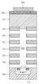
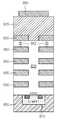
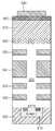
도 2a 내지 2f는 EL 지문인식센서의 단위 화소 단면 구조를 예시적으로 도시한 도면이다.Figs. 2A to 2F are views showing, by way of example, a unit pixel sectional structure of an EL fingerprint recognition sensor. Fig.
도 2a를 참조하면, EL 지문인식센서의 단위 화소는 수광부(210)가 형성된 기판(200), 광입사 경로(220)를 형성하는 복수의 메탈 라인(230, 235, 240, 245, 250, 255), 메탈 라인(255)의 상부에 위치한 발광층(270), 발광층(270)의 상부에 위치한 유전체층(280) 및 유전체층(280)의 상부에 위치한 패턴화된 접촉 전극(290)을 포함한다.2A, a unit pixel of the EL fingerprint sensor includes a
수광부(210)는 플로팅 게이트 구조의 트랜지스터형 수광부이다. 도 2a에 도시된 광입사 경로(220)의 높이와 폭에 의해 결정된 시야각에 의해 수광부(210)는 인접한 다른 단위 화소와 겹치지 않는 범위 이내에서 명암을 구분할 수 있다. 플로팅 게이트 구조의 트렌지스터형 수광부를 단위 화소에 이용하면, 픽셀피치 대비 수광부의 면적이 작고 구조적으로 인접한 메탈 라인을 사용해야 하므로, 메탈 라인을 이용한 광입사 경로의 폭을 더욱 좁힐 수 있다. 따라서, 도 2a에 도시된 바와 같이, 복수의 메탈 라인(230, 235, 240, 245, 250, 255)을 이용하여 광입사 경로의 높이를 증가시키면, 광입사 경로가 좁고 긴 터널형으로 형성될 수 있다. 이에 따라 경사광 차단율이 증가하여 광량은 감소하지만, 플로팅 게이트 구조의 트랜지스터형 수광부의 높은 광 감도특성으로 인해 적은 광량에서도 선명한 지문이미지를 얻을 수 있다.The
복수의 메탈 라인(230, 235, 240, 245, 250, 255)은 전기 배선을 형성하는 제1 및 제2 메탈 라인(230, 235), 더미 메탈 라인인 제3 및 제4 메탈 라인(240, 245), 및 전계를 유도하기 위한 제5 및 제6 메탈 라인(250, 255)으로 구성된다. 제1 내지 제6 메탈 라인(230, 235, 240, 245, 250, 255)은 IMD(Inter Metal Dielectric)에 의해 상호간에 전기적으로 절연된다. 또한, 제1 내지 제6 메탈 라인(230, 235, 240, 245, 250, 255)에 의해 정의된 광입사 경로(220)도 IMD로 형성된다. 여기서, 광입사 경로(220)의 단면은 다각형, 원형 등과 같이 다양한 형태로 형성될 수 있다.The plurality of
하위 메탈 라인인 제1 및 제2 메탈 라인(230, 235)은 복수의 메탈 라인 중 수광부(210)에 가장 근접하게 위치한다. 제1 및 제2 메탈 라인(230, 235)은 수광부(210)의 작동을 제어하는 수광부 제어 신호를 전달하고, 수광부(210)가 직진광을 검출하여 생성한 입사광 검출 신호를 전달하는 전기 배선을 형성한다. 일 실시예로, 제1 및 제2 메탈 라인(230, 235)은 수광부(210) 상부의 광입사 경로(220)를 둘러싸도록 배치될 수 있다. 다른 실시예로, 제1 및 제2 메탈 라인(230, 235) 중 전기 배선을 형성하지 메탈 라인이 수광부(210) 상부의 광입사 경로(220)를 둘러싸도록 배치될 수도 있다. 제1 및 제2 메탈 라인(230, 235)에 의해 정의되는 광입사 경로(220)의 단면은 다각형, 원형 등과 같이 다양한 형태로 형성될 수 있다.The first and
제3 및 제4 메탈 라인(240, 245)은 제1 및 제2 메탈 라인(230, 235)과 제5 및 제6 메탈 라인(250, 255) 사이에 위치한다. 일 실시예로, 더미 메탈 라인인 제3 및 제4 메탈 라인(240, 245)은 제1 및 제2 메탈 라인(230, 235)과 제5 및 제6 메탈 라인(250, 255)에 의해 형성된 광입사 경로(220)에 대응하는 위치에 형성된 개구를 포함하는 평판 형태로 형성될 수 있다. 제3 및 제4 메탈 라인(240, 245)에 형성된 개구는 광입사 경로(220)를 정의한다. 개구는 다각형, 원형 등과 같이 다양한 형태로 형성될 수 있다. 한편, 더미 메탈 라인은 도 2a에 도시된 바와 같이 반드시 복수일 필요는 없으며, 수광부의 종류나 요구되는 광입사 경로의 높이-폭 비율에 따라 하나의 더미 메탈 라인만이 제1 및 제2 메탈 라인(230, 235)과 제5 및 제6 메탈 라인(250, 255) 사이에 위치할 수도 있다.The third and
상위 및 최상위 메탈 라인인 제5 및 제6 메탈 라인(250, 255)은 복수의 메탈 라인 중 수광부(210)에 가장 멀리 위치한다. 제6 메탈 라인(255)은 접촉 전극(290)과 전계를 형성하기 위해 교류 전원에 연결되며, 제5 메탈 라인(250)은 형성된 전계가 하부에 위치한 나머지 메탈 라인들(230, 235, 240, 245)에 영향을 미치지 않도록 하기 위해 접지에 연결될 수 있다. 제5 및 제6 메탈 라인(250, 255)은 제1 내지 제4 메탈 라인(230, 235, 240, 245)에 의해 형성된 광입사 경로(220)에 대응하는 위치에 형성된 개구를 포함하는 평판 형태로 형성될 수 있다. 일 실시예로, 제6 메탈 라인(255) 상면의 적어도 일부가 발광층(270)의 하면에 전기적으로 접촉할 수 있다. 여기서, 제6 메탈 라인(255) 상면의 적어도 일부는 광입사 경로(220)의 주변이다. 다른 실시예로, 제6 메탈 라인(255) 상면의 적어도 일부 및 광입사 경로(220)측에 위치한 제6 메탈 라인(255) 측면의 적어도 일부가 발광층(270)에 전기적으로 접촉할 수 있다. 제5 및 제6 메탈 라인(250, 255)에 의해 정의되는 광입사 경로의 단면은 다각형, 원형 등과 같이 다양한 형태로 형성될 수 있다. 한편, 또 다른 실시예로, 하나 이상의 더미 메탈 라인이 형성되면, 제5 메탈 라인(250)은 생략될 수 있다.The fifth and
발광층(270)은 제6 메탈 라인(255)의 상부에 발광 물질로 형성된다. 발광층(270)은 접촉 전극(290)과 제6 메탈 라인(255) 사이에 형성된 전계에 의해 빛을 발생한다. 발광 물질은, 예를 들어, ZnS, SrS 등과 같은 II - VI족 화합물에서 선택될 수 있다. 한편, 발광 물질은 발광 휘도 및/또는 색상을 조절하기 위해, 예를 들어, Mn, Cu, Al, I, Tb, F 등과 같은 도펀트로 도핑될 수 있다. 예를 들어, 포토 다이오드로 구성된 수광부는 청색에 대한 감도가 낮은 반면, 플로팅 게이트 구조의 트렌지스터형 수광부는 청색에 대한 감도가 높다. 따라서 어떤 수광부가 단위 화소에 적용되는지에 따라 도펀트 또는 도펀트의 조합이 결정될 수 있다.The
유전체층(280)은 발광층(270)의 상부에 형성된다. 유전체층(280)은 접촉 전극(290)과 지문간 접촉에 의한 전계가 형성될 수 있도록, 예를 들어, HfO2, Al2O3, ZrO2, TaO2, Ta2O5, 하프늄 실리케이트, 지르코늄 실리케이트 또는 이들의 조합 등과 같은 높은 유전율을 갖는 물질로 형성된다. 지문의 융선이 접촉 전극(290)에 접촉하면, 유전체층(280)의 높은 유전율로 인해 발광층(270) 내부에 전계를 발생시키는 전기적 연결이 형성될 수 있다.The
접촉 전극(290)은 유전체층(280)의 상부에 형성되며, 유전체층(280)을 통해 발광층(270)의 상면과 전기적으로 접촉한다. 접촉 전극(290)은 예를 들어, ITO(Indium Tin Oxide) 등과 같은 투명 전극 또는 Al, Cu, Au, Ag 등과 같은 금속 전극일 수 있다. 접촉 전극(290)은 원형 등과 같이 다양한 형태로 형성될 수 있다. 접촉 전극(290)은 유전체층(280)의 상면에 수평한 방향으로 연장될 수 있다.The
도 2b를 참조하면, EL 지문인식센서의 단위 화소는 수광부(210)가 형성된 기판(200), 광입사 경로(220)를 형성하는 복수의 메탈 라인(230, 235, 247, 250, 255), 메탈 라인(255)의 상부에 위치한 발광층(270), 발광층(270)의 상부에 위치한 유전체층(280) 및 유전체층(280)의 상부에 위치한 패턴화된 접촉 전극(290)을 포함한다. 도 2a와 중복되는 설명은 생략하고, 차이점을 위주로 설명한다.2B, a unit pixel of the EL fingerprint sensor includes a
제3 메탈 라인(247)은 더미 메탈 라인이며, 복수의 메탈 라인 중 제1 및 제2 메탈 라인(230, 235)과 제4 및 제5 메탈 라인(250, 255) 사이에 위치한다. 제3 메탈 라인(247)은 나머지 메탈 라인들(230, 235, 250, 255)보다 두껍게 형성된다. 제3 메탈 라인(247)의 두께를 두껍게 형성하면, 복수의 더미 메탈 라인으로 확보할 수 있는 높이-폭 비율을 구현하면서도 공정을 생략할 수 있다.The
도 2c를 참조하면, EL 지문인식센서의 단위 화소는 수광부(210)가 형성된 기판(200), 광입사 경로(220)를 형성하는 복수의 메탈 라인(230, 237, 250, 255), 메탈 라인(255)의 상부에 위치한 발광층(270), 발광층(270)의 상부에 위치한 유전체층(280) 및 유전체층(280)의 상부에 위치한 패턴화된 접촉 전극(290)을 포함한다. 도 2a와 중복되는 설명은 생략하고, 차이점을 위주로 설명한다.Referring to FIG. 2C, the unit pixel of the EL fingerprint sensor includes a
하위 메탈 라인인 제1 및 제2 메탈 라인(230, 237)은 복수의 메탈 라인 중 수광부(210)에 가장 근접하게 위치한다. 제1 및 제2 메탈 라인(230, 237)은 수광부(210)의 작동을 제어하는 수광부 제어 신호를 전달하고, 수광부(210)가 직진광을 검출하여 생성한 입사광 검출 신호를 전달하는 전기 배선을 형성한다. 제2 메탈 라인(237)은 나머지 메탈 라인들(230, 250, 255)보다 두껍게 형성된다. 제2 메탈 라인(237)의 두께를 두껍게 형성하면, 하나 이상의 더미 메탈 라인으로 확보할 수 있는 높이-폭 비율을 구현하면서도 더미 메탈 라인을 형성하는 공정을 생략할 수 있다.The first and
도 2d를 참조하면, EL 지문인식센서의 단위 화소는 수광부(210)가 형성된 기판(200), 광입사 경로(220)를 형성하는 복수의 메탈 라인(230, 235, 251, 255), 메탈 라인(255)의 상부에 위치한 발광층(270), 발광층(270)의 상부에 위치한 유전체층(280) 및 유전체층(280)의 상부에 위치한 패턴화된 접촉 전극(290)을 포함한다. 도 2a와 중복되는 설명은 생략하고, 차이점을 위주로 설명한다.2D, the unit pixel of the EL fingerprint sensor includes a
상위 및 최상위 메탈 라인인 제3 및 제4 메탈 라인(251, 255)은 복수의 메탈 라인(230, 235, 251, 255) 중 수광부(210)에 가장 멀리 위치한다. 제3 메탈 라인(251)은 형성된 전계가 하부에 위치한 나머지 메탈 라인들(230, 235)에 영향을 미치지 않도록 하기 위해 접지에 연결된다. 제3 메탈 라인(251)은 나머지 메탈 라인들(230, 235, 255)보다 두껍게 형성된다. 제3 메탈 라인(251)의 두께를 두껍게 형성하면, 하나 이상의 더미 메탈 라인으로 확보할 수 있는 높이-폭 비율을 구현하면서도 더미 메탈 라인을 형성하는 공정을 생략할 수 있다.The third and
도 2e를 참조하면, EL 지문인식센서의 단위 화소는 수광부(215)가 형성된 기판(200), 광입사 경로(225)를 형성하는 복수의 메탈 라인(230, 235, 240, 245, 250, 255), 메탈 라인(255)의 상부에 위치한 발광층(270), 발광층(270)의 상부에 위치한 유전체층(280) 및 유전체층(280)의 상부에 위치한 패턴화된 접촉 전극(290)을 포함한다. 도 2a와 중복되는 설명은 생략하고, 차이점을 위주로 설명한다.2E, the unit pixel of the EL fingerprint sensor includes a
수광부(215)는 광전 변환을 위한 포토 다이오드이다. 포토 다이오드는 도 2a에 도시된 플로팅 게이트 구조의 트렌지스터형 수광부(210)에 비해 상대적으로 큰 광량이 요구되기 때문에, 광입사 경로(225)의 높이가 도 2a에 도시된 광입사 경로(210)의 높이와 동일한 경우, 광입사 경로(225)의 폭이 증가되어야 한다. 광입사 경로의 폭이 증가하면, 제6 메탈 라인(255)과 접촉하는 발광층(270)의 면적이 감소하고, 광입사 경로(225)에 노출되는 발광층(270)의 면적이 증가하므로, 수광부(225)에 입사되는 광량이 증가한다. 따라서, 광전 변환 효율이 낮은 포토 다이오드가 적용되더라도 충분히 선명한 지문이미지를 얻을 수 있다.The
도 2f를 참조하면, EL 지문인식센서의 단위 화소는 수광부(215)가 형성된 기판(200), 광입사 경로(225)를 형성하는 복수의 메탈 라인(230, 235, 247, 250, 255), 메탈 라인(255)의 상부에 위치한 발광층(270), 발광층(270)의 상부에 위치한 유전체층(280) 및 유전체층(280)의 상부에 위치한 패턴화된 접촉 전극(290)을 포함한다. 도 2a 및 2e와 중복되는 설명은 생략하고, 차이점을 위주로 설명한다.Referring to FIG. 2F, the unit pixel of the EL fingerprint sensor includes a
제3 메탈 라인(247)은 더미 메탈 라인이며, 제1 및 제2 메탈 라인(230, 235)과 제4 및 제5 메탈 라인(250, 255) 사이에 위치한다. 제3 메탈 라인(247)은 나머지 메탈 라인들(230, 235, 250, 255)보다 두껍게 형성된다. 제3 메탈 라인(247)의 두께를 두껍게 형성하면, 복수의 더미 메탈 라인으로 확보할 수 있는 높이-폭 비율을 구현하면서도 공정을 생략할 수 있다.The
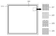
도 3은 EL 지문인식센서의 지문접촉면의 구조를 예시적으로 도시한 도면이다.3 is a view showing an exemplary structure of the fingerprint contact surface of the EL fingerprint recognition sensor.
도 3을 참조하면, EL 지문인식센서의 상면은 지문이미지를 획득할 손가락과 교류 전원간 전기적인 경로를 형성하기 위한 제1 영역(310) 및 지문과 접촉하기 위해 복수의 단위 화소의 접촉 전극이 배열되는 제2 영역(320)을 포함한다. 제1 영역(310)과 제2 영역(320)은 전기적으로 절연되어 있다.Referring to FIG. 3, the upper surface of the EL fingerprint sensor includes a
제1 영역(310)은 제2 영역(320)의 외곽에 형성된다. 제1 영역(310)은 지문이미지를 획득할 손가락과 교류 전원간 전기적인 경로를 형성하기 위하여 접지에 전기적으로 연결된다. 제1 영역(310)은 ITO 또는 금속과 같이 전기 전도성이 높은 물질로 형성된다. 한편 제1 영역(310)은 제2 영역(320) 외곽의 일부에 형성될 수도 있다.The
제2 영역(320)에는 도 2a 내지 2f에 도시된 단위 화소의 어레이가 배치된다. 단위 화소의 어레이는 접촉 전극의 형상에 따라 배열 방식이 달라질 수 있다. 점선으로 표시된 제2 영역(320)의 일부 영역을 확대하면, 접촉 전극은 정사각형 접촉 전극(321), 원형 접촉 전극(322), 육각형 접촉 전극(323), 마름모형 접촉 전극(324)으로 형성될 수 있다. 정사각형 접촉 전극(321)과 원형 접촉 전극(322)은 동일한 행이나 열에 나란히 배열된다. 육각형 접촉 전극(323)과 마름모형 접촉 전극(324)은 인접하는 행이나 열에 위치한 접촉 전극의 중심이 일치하지 않도록 배열된다.In the
접촉 전극(321, 323, 324)의 최대 폭 또는 접촉 전극(322)의 최대 직경과 접촉 전극(321, 322, 323, 324)의 전극간 거리는 지문이미지 획득을 위해 최적화될 수 있다. 융선-융선간 또는 골-골간 거리인 지문간격은 나이, 성별, 인종에 따라 달라질 수 있다. 지문에는 0.2~0.8mm의 지문간격이 있으며 평균 0.5mm의 간격이 있는 것으로 가정할 수 있다. 따라서, 접촉 전극(321, 323, 324)의 최대 폭 또는 접촉 전극(322)의 최대 직경은 0.2mm 내지 0.5mm 사이일 수 있다.The maximum width of the
도 3에 도시된 접촉 전극(321, 322, 323, 324)의 형상 및 배열 방식은 단지 예시일 뿐 이에 한정되지 않는다.The shape and arrangement of the
도 4는 EL 지문인식센서의 동작을 예시적으로 도시한 도면이다.FIG. 4 is a diagram illustrating an exemplary operation of the EL fingerprint recognition sensor.
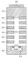
도 4를 참조하면, EL 지문인식센서는 수광부(410), 복수의 메탈 라인(430, 435, 440, 445, 450, 455), 메탈 라인(455)의 상부에 위치한 발광층(470), 발광층(470)의 상부에 위치한 유전체층(480) 및 유전체층(480)의 상부에 위치한 패턴화된 접촉 전극(490)을 포함하는 복수의 단위 화소를 배열하여 구현될 수 있다. 여기서, 복수의 메탈 라인(430, 435, 440, 445, 450, 455) 중 인접하는 두 개의 메탈 라인 사이에 더미 비아(441, 442)가 더 형성될 수 있다. 더미 비아(441, 442)는 광입사 경로(420)로 입사된 경사광이 인접한 다른 단위 화소를 향해 반사되지 않도록 차단한다.4, the EL fingerprint recognition sensor includes a
배열된 복수의 접촉 전극 중 지문의 융선에 접촉한 접촉 전극(491)과 제6 메탈 라인(455) 사이에 전계(471)가 유도된다. 손가락의 일부는 접지된 제2 영역(도 3의 320)에 접촉하고, 제6 메탈 라인(455)은 교류 전원에 연결되므로, 발광층(470) 내부에 전계(471)가 유도된다. 여기서, 교류 전원은 약 60 내지 약 600 볼트 사이의 교류 전압을 제6 메탈 라인(455)에 인가할 수 있다. 상세하게, 패턴화된 접촉 전극(490) 및 광입사 경로(420)를 정의하는 제6 메탈 라인(455)으로 인해, 지문의 융선과 접촉한 접촉 전극(491) 하부에 위치한 발광층(470)의 일부에 전계(471)가 유도된다. 여기서, 전계(471)가 유도된 발광층(470)의 일부가 발생하는 빛은 방향성을 가지지 않는다. 즉, 주변의 다른 접촉 전극-제6 메탈 라인간 전계에 의해 발생된 빛이 입사될 수도 있다. 따라서 접촉 전극의 하부에 정의되는 광입사 경로(420)의 높이-폭 비율이 클수록 주변에서 입사되는 경사광이 효과적으로 차단될 수 있다.An
발생된 빛의 일부는 발광층(470)의 하면(472)으로부터 광입사 경로(420)로 입사된다. 입사된 빛은 직진광과 경사광을 포함하며, 이중에서 경사광은 제1 내지 제6 메탈 라인(430, 435, 440, 445, 450, 455) 및 더미 비아(441, 442)에 의해 차단되거나 반사된다. 광입사 경로를 통과한 직진광은 기판(400)에 형성된 수광부(410)에 의해 광전변환된다. 지문의 융선과 접촉한 접촉 전극(491)의 하부에 위치한 수광부(410)는 입사광 검출 신호를 출력하며, 지문의 골에 위치한 접촉 전극의 하부에 위치한 수광부(410)는 입사광 검출 신호를 출력하지 않는다.A part of the generated light is incident on the
도 5는 EL 지문인식센서의 더미 메탈 라인의 구조를 예시적으로 도시한 도면이다.FIG. 5 is a view showing an exemplary structure of a dummy metal line of the EL fingerprint recognition sensor.
도 5를 참조하면, 더미 메탈 라인(540, 545)은 광입사 경로를 정의하는 복수의 개구(546)가 형성된 평판일 수 있다. 한 쌍의 더미 메탈 라인(540, 545)은 복수의 더미 비아(541, 542, 543)에 의해 연결될 수 있다. 복수의 더미 비아(541, 542, 543)는 광입사 경로를 정의하는 개구(546) 주변에 형성된다. 개구(546) 주변에 형성된 복수의 더미 비아(541, 542, 543)는 광입사 경로에 들어온 경사광이 인접한 단위 화소의 광입사 경로로 들어가는 것을 방지한다. 더미 비아의 수와 형상은 개구의 형상에 따라 달라질 수 있다. 도 5에 도시된 바와 같이, 개구(546)가 사각형 형태로 더미 메탈 라인(540, 545)에 형성되면, 더미 비아(541, 542, 543)는 사각형의 각 변에 인접한 위치에 형성될 수 있다.Referring to FIG. 5, the
도 6은 도 2에 도시된 플로팅 게이트 구조의 트랜지스터형 수광부를 도시한 회로도와 동작 원리를 설명하기 위한 예시도이다.FIG. 6 is a circuit diagram showing the transistor-type light-receiving portion of the floating gate structure shown in FIG. 2 and an example for explaining the operation principle thereof.
단위 화소(600)는 빛을 광전변환하여 입사광 검출 신호를 출력한다. 이를 위해, 단위 화소(600)는 입사된 빛을 광전변환하는 수광부 역할을 하는 PMOS(610)와 PMOS(610)에 연결되어 스위치 역할을 하는 NMOS(620)로 구성된다. 여기서, PMOS(610)는 입사된 빛으로 분극된 플로팅 게이트에 의한 전계로 소스와 드레인간 형성된 채널을 흐르는 입사광 검출 신호의 크기를 제어하며, NMOS(620)는 셀렉트 트랜지스터로서 입사광 검출 신호를 출력할 단위 화소(600)를 선택하고 노출 시간을 결정하는 기능을 수행한다. NMOS(620)는 제어 게이트에 인가되는 SEL 제어 신호에 의해 스위칭 동작을 하며, SEL 제어 신호는 전원전압 VDD보다 큰 전압 신호일 수 있다. 여기서, NMOS는 Vth가 낮은 Native 또는 Medium Vt의 트랜지스터일 수 있다.The unit pixel 600 photoelectrically converts light and outputs an incident light detection signal. To this end, the unit pixel 600 includes a PMOS 610 serving as a light receiving part for photoelectrically converting incident light, and an NMOS 620 connected to the PMOS 610 and serving as a switch. Here, the PMOS 610 controls the magnitude of the incident light detection signal flowing through the channel formed by the electric field source and the drain by the floating gate polarized by the incident light, and the NMOS 620 outputs the incident light detection signal as the select transistor Selects a unit pixel 600 and determines an exposure time. The NMOS 620 performs a switching operation by a SEL control signal applied to the control gate, and the SEL control signal may be a voltage signal that is higher than the power supply voltage VDD. Here, the NMOS may be a Native or Medium Vt transistor having a low Vth.
PMOS(610)의 소스는 전원전압 VDD에 결합되며, 드레인은 NMOS(620)의 드레인에 결합된다. PMOS(610)의 바디는 플로팅 바디로 형성되며, NMOS(620)의 바디는 접지전압 GND에 연결된다. 한편, 픽셀 영역에서 NMOS(620)의 바디 혹은 P-well은 플로팅 바디로도 형성될 수 있다. NMOS(620)의 소스는 입사광 검출 신호를 출력하며, 출력된 입사광 검출 신호는 IVC(I-V Converter)에 인가될 수 있다. PMOS(610) 및 NMOS(620)는 일반적인 MOSFET 공정을 통해 구현될 수 있다.The source of the PMOS 610 is coupled to the power supply voltage VDD and the drain is coupled to the drain of the NMOS 620. The body of the PMOS 610 is formed of a floating body, and the body of the NMOS 620 is connected to the ground voltage GND. The body or P-well of the NMOS 620 in the pixel region may also be formed as a floating body. The source of the NMOS 620 outputs an incident light detection signal, and the outputted incident light detection signal can be applied to an IVC (I-V Converter). The PMOS 610 and the NMOS 620 may be implemented through a general MOSFET process.
단위 화소(600)의 동작은 다음과 같다. NMOS(620)와 동일한 기판상에 형성된 PMOS(610)의 소스에 전원전압 VDD를 인가하면, N-well과 p형 기판이 대면하는 모든 영역에서 PN접합면이 형성되고 역바이어스로 인해서 전기적으로 중성상태인 공핍영역이 두껍게 형성된다. 또한 전원전압은 PMOS(610)의 소스와 드레인사이에 전계에 의해서 P채널이 유도된다. 이후, 수광부인 PMOS(610)로 빛이 입사되면, 광자가 플로팅 게이트와 공핍영역이 생성된 N-well의 하부 접합면에 입사되어 전자-정공쌍(EHP; Electron hole pair)이 생성된다. PMOS(610)의 플로팅 게이트에서는 분극 현상으로 인해 플로팅 게이트의 하부에 위치한 N-well, 즉, 드레인과 소스 사이에 P채널을 완성하게 된다. PMOS(610)와 연결된 NMOS(620)의 게이트에 전압이 인가되고 NMOS(620)에 형성된 소스와 드레인 사이에 채널이 형성되어 PMOS(610)에 형성된 신호 전하를 받아 입사광 검출 신호를 출력한다. 종래의 씨모스 이미지 센서는 하나의 광자가 하나의 전자-정공쌍을 생성시키는 반면, 단위 화소(600)의 PMOS(610)는 하나의 광자가 증폭된 PMOS의 채널전류를 유도한다. 따라서, 입사광 검출 신호의 전류 이득이 100~1000에 달하여 소량의 빛이 입사되는 저조도에서도 영상의 구현이 가능하다.The operation of the unit pixel 600 is as follows. When the power source voltage VDD is applied to the source of the PMOS 610 formed on the same substrate as the NMOS 620, a PN junction is formed in all regions where the N-well and the p-type substrate face each other, The depletion region is formed thick. Also, a power source voltage is a P-channel induced between the source and the drain of the PMOS 610 by an electric field. Thereafter, when light is incident on the PMOS 610 as a light receiving part, the photon is incident on the lower junction surface of the N-well in which the floating gate and the depletion region are generated, thereby generating an electron hole pair (EHP). In the floating gate of the PMOS transistor 610, the P-channel is formed between the N-well, that is, the drain and the source, located under the floating gate due to the polarization phenomenon. A voltage is applied to the gate of the NMOS 620 connected to the PMOS 610 and a channel is formed between the source and the drain formed in the NMOS 620 to receive the signal charge formed in the PMOS 610 and output an incident light detection signal. In the conventional CMOS image sensor, one photon produces one electron-hole pair, while the PMOS 610 of the unit pixel 600 induces a channel current of the PMOS in which one photon is amplified. Accordingly, it is possible to realize an image even in a low light level in which a current gain of an incident light detection signal reaches 100 to 1000 and a small amount of light is incident.
플로팅 게이트(613a, 613b, 613c)는 N-로 도핑된 폴리실리콘으로 형성될 수 있으며, 빛의 흡수 파장대를 넓게 하기 위해 100nm 내지 1um의 두께로 형성될 수 있다. 일반적인 MOSFET 공정에 따라 제작되는 경우, 플로팅 게이트(613a, 613b, 613c)는 200~300nm의 두께로 형성되며 400nm 이하의 단파장은 대부분 흡수하지만, 가시광의 장파장대역, 예를 들어, 500~1,100nm은 상당량 투과시킨다. 따라서 투과율이 높은 장파장대역의 흡수율을 높이기 위해서 플로팅 게이트(613a, 613b, 613c)의 두께를 증가시킬 수 있다. 플로팅 게이트(613)의 두께 증가로 인해 플로팅 게이트(613a, 613b, 613c) 내에서 빛에 의한 EHP 생성 확률이 증가될 수 있다. 또한 PIP(polysilicon-insulator-polysilicon) 커패시터 방식을 지원하는 공정에서는, 폴리실리콘을 적층시키고 수직으로 서로 연결하여 게이트로 이용함으로써, 플로팅 게이트(613a, 613b, 613c)의 두께를 증가시킨 것과 같은 효과를 줄 수 있다. 한편, 플로팅 게이트(613a, 613b, 613c)의 두께를 증가시킴으로써, N-well 및/또는 P형 기판 내부까지 입사한 빛에 의한 EHP 생성을 감소시킬 수도 있다.The floating gates 613a, 613b, and 613c may be formed of N-doped polysilicon and may be formed to have a thickness of 100 nm to 1 um to widen the absorption wavelength band of light. When manufactured according to a general MOSFET process, the floating gates 613a, 613b, and 613c are formed to have a thickness of 200 to 300 nm, and most of short wavelengths of 400 nm or less are absorbed, but long wavelength bands of visible light, . Therefore, the thickness of the floating gates 613a, 613b, and 613c can be increased to increase the absorption ratio in the long wavelength band having a high transmittance. The increase in the thickness of the floating gate 613 can increase the probability of EHP generation due to light in the floating gates 613a, 613b, and 613c. Further, in a process that supports a polysilicon-insulator-polysilicon (PIP) capacitor method, polysilicon is stacked and vertically connected to each other as a gate to increase the thickness of the floating gates 613a, 613b, and 613c You can give. On the other hand, by increasing the thickness of the floating gates 613a, 613b, and 613c, it is possible to reduce EHP generation due to light incident into the N-well and / or P-type substrate.
좌측에 도시된 플로팅 게이트(613a)는 빛이 조사되지 않은 상태에서의 전자 분포를 나타낸다. 계면 전류(Surface current)에 의한 노이즈 발생을 최소화하는 Buried Channel을 PMOS 소스와 PMOS 드레인 사이에 형성하기 위해, 플로팅 게이트(613a)는 N-로 도핑된다. 여기서, 좌측 하단은 PMOS 소스측을 향하고 있으며, 우측 하단은 PMOS 드레인측을 향한다.The floating gate 613a shown on the left side shows the electron distribution in the state where no light is irradiated. The floating gate 613a is N- doped to form a buried channel between the PMOS source and the PMOS drain that minimizes the noise generation due to the surface current. Here, the left lower end faces the PMOS source side, and the lower right end faces the PMOS drain side.
중앙에 도시된 플로팅 게이트(613b)는 빛이 입사되어 EHP가 생성되고 전자와 정공이 분극되어 외부 전계에 의해 분포하는 상태를 나타낸다. 플로팅 게이트(613b)에서, 정공에서 분리된 전자는 폴리실리콘의 그레인 경계의 외부에서 자유롭게 이동할 수 있으며, PMOS 소스의 전계효과로 인해 플로팅 게이트(613b)의 좌측 하단, 즉, PMOS 소스에 가까운 위치에 집중된다. 전자가 집중되면서 플로팅 게이트(613b)의 좌측 하부에는 전계가 형성되며, 집중되는 전자의 수가 증가할수록 전계도 강해진다. 한편, 정공은 PMOS 소스와 하부의 채널의 홀 캐리어에 밀려서 플로팅 게이트(613b)의 우측 상단, 즉, PMOS 소스에서 먼 쪽으로 전하(carrier)가 이동하면서 플로팅 게이트(613b) 내부에서 분극 현상이 발생한다. 빛이 사라지면, 분극되었던 전자와 정공은 열적 평형상태가 되기 위해 재결합되어 다시 좌측(613a)과 같은 상태가 된다.The floating gate 613b shown at the center shows a state in which light is incident to generate EHP and electrons and holes are polarized and distributed by an external electric field. In the floating gate 613b, the electrons separated from the holes can freely move outside the grain boundary of the polysilicon, and due to the electric field effect of the PMOS source, they are located at the lower left of the floating gate 613b, It is concentrated. As electrons are concentrated, an electric field is formed in the lower left portion of the floating gate 613b, and the electric field becomes stronger as the number of concentrated electrons increases. On the other hand, the holes are pushed by the hole carriers of the PMOS source and the lower channel, and the carriers move to the upper right side of the floating gate 613b, that is, away from the PMOS source, and polarization occurs in the floating gate 613b . When the light disappears, the polarized electrons and holes recombine to become a thermal equilibrium state and become the same state as the left side (613a) again.
우측은 분극 현상이 발생한 플로팅 게이트(613c)이다. 입사된 빛의 세기가 클수록 EHP 생성이 많아지므로, 따라서 분극 현상도 크게 나타난다. 플로팅 게이트(613c)의 분극 현상으로 인하여 플로팅 게이트(613c)의 하면과 채널의 상면에 전계효과가 작용하면 입사된 빛의 세기에 따라 플로팅 게이트(613c)의 하면의 전하가 증가하여 전계가 크게 걸리는 효과가 나타난다. 이로 인해, PMOS 소스와 PMOS 드레인간 채널이 확장하여 채널을 통해서 흐르는 전류량이 증가하게 된다.And the right side is a floating gate 613c in which a polarization phenomenon occurs. The larger the intensity of the incident light, the more EHP production is generated. If the electric field effect is applied to the lower surface of the floating gate 613c and the upper surface of the channel due to the polarization of the floating gate 613c, the charge of the lower surface of the floating gate 613c increases in accordance with the intensity of the incident light, Effect appears. As a result, the PMOS source and the PMOS drain channel expand and the amount of current flowing through the channel increases.
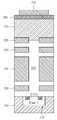
도 7은 EL 지문인식센서의 제조 과정을 예시적으로 도시한 도면이다.FIG. 7 is a diagram illustrating an exemplary manufacturing process of the EL fingerprint recognition sensor.
도 7의 (a)를 참조하면, P형 기판(700)에 N형 불순물을 주입하여 N-well이 형성되며, N-well에 소스 및 드레인이 구성되며 N-well의 상부에는 절연층이 형성된 후 폴리실리콘으로 증착 형성된 플로팅 게이트가 구비된 PMOS 수광부(710)가 형성된다. 수광부(710)의 상부에는 전기 배선을 형성하는 제1 메탈 라인(730) 및 제2 메탈 라인(735)이 형성된다. 제2 메탈 라인(735)의 상부에, 광입사 경로(720)의 높이를 증가시키기 위한 더미 메탈 라인인 제3 메탈 라인(740)과 제4 메탈 라인(745), 전계 차단을 위한 제5 메탈 라인(750), 및 교류 전원에 연결되는 제6 메탈 라인(755)이 차례로 적층된다. 제1 내지 제6 메탈 라인(730, 735, 740, 745, 750, 755)는 IMD에 의해 절연되며, 광입사 경로(720)도 IMD로 형성된다.7A, an N-well is formed by implanting N-type impurity into a P-
도 7의 (b)를 참조하면, 제6 메탈 라인(755)의 상부에 발광 물질을 이용하여 발광층(770)이 형성된다. 발광 물질은, 예를 들어, ZnS, SrS 등과 같은 II - VI족 화합물에서 선택될 수 있다. 한편, 발광 물질은 발광 휘도 및/또는 색상을 조절하기 위해, 예를 들어, Mn, Cu, Al, I, Tb, F 등과 같은 도펀트로 도핑될 수 있다. 예를 들어, 파우더 형태의 발광 물질은 Polymeric matrix 등과 같은 바인더와 혼합되어 액상으로 바뀐 후, spin coating, dip coating 등에 의해 제6 메탈 라인(755)의 상부에 코팅될 수 있다.Referring to FIG. 7 (b), a
한편, 발광 물질의 입자 크기에 따라 휘도 및 인가될 교류 전원이 달라질 수 있다. 즉, 발광 물질의 입자 크기가 작아질수록 휘도는 증가하며, 인가될 교류 전원이 낮아질 수 있다. 따라서, 발광 물질은 나노 결정 파우더 형태일 수 있다. 나노 결정 파우더를 수지와 유기 용매에 분산시켜 나노 입자 용액을 생성한다. 여기서, 나노 결정 파우더는 ZnS:Mn, ZnS:Ag ZnS:Al 등일 수 있다. 일 실시예로, 기판을 나노 입자 용액에 담그는 Dip coating 또는 나노 입자 용액을 회전하는 기판 위에 떨어뜨리는 Spin casting 등의 방식을 이용하여, 제6 메탈 라인(755)의 상부에 발광층(770)이 형성될 수 있다. 한편, 발광층(770)은 나노 입자 용액을 기판 위에 인쇄하는 방식으로도 형성될 수 있다. 나노 입자 용액을 이용하여 발광층을 형성하는 방식은, 상술한 dip coating/spin coating 이외에도, microcontact printing, inkjet printing, electgrospray 등 다양하게 적용될 수 있다. 기판에 도포된 나노 입자 용액을 건조하여 발광층(770)이 형성될 수 있다. 다른 실시예로, 발광층(770)은 나노 결정 파우더를 RF magnetron 스퍼터링을 이용하여 제6 메탈 라인(755) 상부에 증착하여 형성될 수 있다. 또 다른 실시예로, 발광층(770)은 나노 결정 파우더, 예를 들어, ZnS:Mn과 Si3N4를 번갈아 제6 메탈 라인(755) 상부에 증착하여 형성될 수도 있다. 여기서, ZnS:Mn로 형성된 층은 Si3N4로 형성된 층보다 두꺼울 수 있다. 한편, 발광층(770)의 발광 효율은 나노 결정의 크기에 따라 달라질 수 있다. 나노 결정의 크기가 작을수록 발광 효율이 증가한다.On the other hand, the luminance and the AC power to be applied may vary depending on the particle size of the light emitting material. That is, as the particle size of the luminescent material becomes smaller, the luminance increases, and the AC power to be applied may be lowered. Thus, the luminescent material may be in the form of nanocrystalline powder. Nanocrystalline powder is dispersed in resin and organic solvent to produce nanoparticle solution. Here, the nanocrystalline powder may be ZnS: Mn, ZnS: Ag ZnS: Al, or the like. In one embodiment, a
도 7의 (c)를 참조하면, 발광층(770)의 상부에 유전체층(780)이 형성된다. 유전체층(780)은 Al2O3 HfO2등과 같은 유전체를 RF magnetron 스퍼터링에 의해 형성될 수 있다. 한편, 유전체층(780)은 파우더 형태의 유전체에 바인더를 혼합한 액상 유전체를 제6 메탈 라인(755)의 상부에 dip coating 또는 spin coating하여 형성될 수도 있다.Referring to FIG. 7 (c), a
도 7의 (d)를 참조하면, 접촉 전극(790)은 유전체층(780)의 상부에, 광입사 경로(720)에 대응하는 위치에 형성된다. 접촉 전극(790)은 ITO 등과 같은 투명 전극 또는 Al, Cu, Au, Ag 등과 같은 금속 전극을 증착하여 형성될 수 있다.7 (d), the
도 8a 내지 8c는 EL 지문인식센서의 다른 단위 화소 단면 구조를 예시적으로 도시한 도면이다.8A to 8C are views showing another example unit pixel cross-sectional structure of the EL fingerprint recognition sensor.
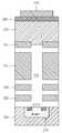
도 8a를 참조하면, EL 지문인식센서의 단위 화소는 수광부(810)가 형성된 기판(800), 광입사 경로(820)를 형성하는 복수의 메탈 라인(830, 835, 840, 850, 855), 메탈 라인(855)의 상부에 위치한 발광층(870), 발광층(870)의 상부에 위치한 패턴화된 접촉 전극(890)을 포함한다. 도 2a와 중복되는 부분은 생략하고 차이점을 위주로 설명한다.8A, a unit pixel of the EL fingerprint sensor includes a
복수의 메탈 라인(830, 835, 840, 850, 855)은 전기 배선을 형성하는 제1 및 제2 메탈 라인(830, 835), 전계를 유도하기 위한 제3 내지 제5 메탈 라인(840, 850, 855)으로 구성된다. 제1 내지 제4 메탈 라인(830, 835, 840, 850)은 IMD(Inter Metal Dielectric)에 의해 상호간에 전기적으로 절연된다. 제4 메탈 라인(850)과 제5 메탈 라인(855) 사이에는 MIM(Metal-Insulator-Metal) 커패시터(852)를 형성하기 위해 고유전율을 갖는 유전물질이 개재된다. 또한, 제1 내지 제5 메탈 라인(830, 835, 840, 850, 855)에 의해 정의된 광입사 경로(820)도 IMD로 형성된다. 여기서, 광입사 경로의 단면은 다각형, 원형 등과 같이 다양한 형태로 형성될 수 있다. 한편, 단위 화소는 광입사 경로(820)의 높이를 증가시키기 위한 더미 메탈을 더 포함할 수 있다. 여기서, 더미 메탈의 두께는 다른 메탈 라인의 두께와 다를 수 있다.The plurality of
제3 내지 제5 메탈 라인(840, 850, 855)은 제1 및 제2 메탈 라인(830, 835)의 상부에 위치되며, 발광층(870)에 전계를 유도한다. 제3 메탈 라인(840)은 형성된 전계가 하부에 위치한 나머지 메탈 라인들(830, 835)에 영향을 미치지 않도록 하기 위해 접지에 연결된다. 제4 메탈 라인(850)과 제5 메탈 라인(855)은 MIM 커패시터(852)에 연결되는 전극이며, 제4 메탈 라인(850)은 교류 전원이 인가되는 공통 전극이고, 제5 메탈 라인(855)은 상면이 발광층(870)에 접하는 개별 전극이다. 여기서, 제4 메탈 라인(850)은 광입사 경로(820)에 대응하는 위치에 형성된 개구를 포함하는 평판 형태로 형성될 수 있다.The third to
상술한 구조를 갖는 단위 화소에서, 제4 메탈 라인(850)에 연결된 교류 전원은 MIM 커패시터(852)에 의해 발광층(870)에 인가된다. 도 2a에 도시된 구조와 비교할 때, 일반적인 반도체 공정이 지원하는 MIM 커패시터를 이용하므로, 접촉 전극(890)을 형성하기 전에 유전체층을 별도로 형성하는 공정이 생략되는 이점이 있다. 즉, 상부에 유전체층을 전체적으로 증착하는 방식보다 발광층을 포함한 단위 화소가 완전히 독립적으로 분리되는 효과가 더 커서 분해능을 높일 수 있고, 정전용량의 값을 조절할 수 있어서 교류전원의 주파수를 조절할 수 있으며 모든 픽셀에서 정전 용량의 균일성이 높도록 제조할 수 있다.In the unit pixel having the above-described structure, the AC power source connected to the
도 8b를 참조하면, EL 지문인식센서의 단위 화소는 수광부(810)가 형성된 기판(800), 광입사 경로(820)를 형성하는 복수의 메탈 라인(830, 835, 840, 850, 855), 메탈 라인(855)의 상부에 위치한 발광층(870), 발광층(870)의 상부에 위치한 유전체층(885) 및 유전체층(885)의 상부에 위치한 패턴화된 접촉 전극(890)을 포함한다. 도 8a와 동일한 설명은 생략하고 차이점만 살펴보면, 발광층(870)은 접촉 전극(890)과는 유전체층(885)을 통해 전기적으로 연결되고, 제4 메탈 라인(850)과는 MIM 커패시터(852)를 통해 전기적으로 연결된다.8B, a unit pixel of the EL fingerprint sensor includes a
도 8c를 참조하면, EL 지문인식센서의 단위 화소는 수광부(810)가 형성된 기판(800), 광입사 경로(820)를 형성하는 복수의 메탈 라인(830, 835, 840, 845, 850, 855), 메탈 라인(855)의 상부에 위치한 발광층(870), 발광층(870)의 상부에 위치한 패턴화된 접촉 전극(890)을 포함한다. 도 8a와 동일한 설명은 생략하고 차이점만 살펴보면, 발광층(870)은 접촉 전극(890) 및 제6 메탈 라인(855)과 직접적으로 연결된다. 제6 메탈 라인(855)을 통해 교류 전원이 인가되며, 접촉 전극(890)에 접촉한 손가락에 의해 발광층(870) 내부에 전계를 유도한다.8C, a unit pixel of the EL fingerprint sensor includes a
한편, 도 8a 내지 8c는 플로팅 게이트 구조의 트랜지스터형 수광부를 도시하고 있으나, 반드시 이에 한정되는 것은 아니며, 포토 다이오드가 수광부로 이용될 수 있음은 물론이다. 포토 다이오드를 수광부로 이용하는 경우, 광입사 경로를 정의하는 복수의 메탈 라인은 도 2e 또는 도 2f와 같이 형성될 수 있다.8A to 8C illustrate the transistor-type light-receiving portion of the floating gate structure, but the present invention is not limited thereto, and it goes without saying that the photodiode may be used as the light-receiving portion. When a photodiode is used as a light receiving portion, a plurality of metal lines defining a light incidence path may be formed as shown in FIG. 2E or 2F.
도 9a 내지 9d는 EL 지문인식센서의 또 다른 단위 화소 단면 구조를 예시적으로 도시한 도면이다.9A to 9D are views showing another example unit pixel cross-sectional structure of the EL fingerprint sensor.
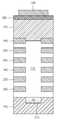
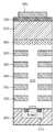
도 9a를 참조하면, EL 지문인식센서의 단위 화소는 수광부(910)가 형성된 기판(900), 광입사 경로(920)를 형성하는 복수의 메탈 라인(930, 935, 940, 945, 950), 최상위 메탈 라인(950)의 상부에 위치한 투명 전극층(960), 투명 전극층(960)의 상부에 위치한 발광층(970), 발광층(970)의 상부에 위치한 유전체층(980) 및 유전체층(980)의 상부에 위치한 패턴화된 접촉 전극(990)을 포함한다. 도 2a와 중복되는 부분은 생략하고 차이점을 위주로 설명한다.9A, the unit pixel of the EL fingerprint sensor includes a
복수의 메탈 라인(930, 935, 940, 945, 950)은 전기 배선을 형성하는 제1 및 제2 메탈 라인(930, 935), 더미 메탈 라인인 제3 및 제4 메탈 라인(940, 945), 및 접지된 제5 메탈 라인(950)으로 구성된다. 제1 내지 제5 메탈 라인(930, 935, 940, 945, 950)은 IMD(Inter Metal Dielectric)에 의해 상호간에 전기적으로 절연된다. 또한, 제1 내지 제5 메탈 라인(930, 935, 940, 945, 950)에 의해 정의된 광입사 경로(920)도 IMD로 형성된다. 여기서, 광입사 경로(920)의 단면은 다각형, 원형 등과 같이 다양한 형태로 형성될 수 있다.The plurality of
최상위 메탈 라인인 제5 메탈 라인(950)은 복수의 메탈 라인 중 수광부(910)에 가장 멀리 위치한다. 제5 메탈 라인(950)은 형성된 전계가 하부에 위치한 나머지 메탈 라인들(930, 935, 940, 945)에 영향을 미치지 않도록 하기 위해 접지에 연결된다. 제5 메탈 라인(950)은 제1 내지 제4 메탈 라인(930, 935, 940, 945)에 의해 형성된 광입사 경로(920)에 대응하는 위치에 형성된 개구를 포함하는 평판 형태로 형성될 수 있다.The
투명 전극층(960)은 제5 메탈 라인(950)의 상부에 위치한다. 투명 전극층(960)의 상면은 발광층(970)의 하면에 접한다. 투명 전극층(960)은 ITO(Indium Tin Oxide), 플루오르틴산화물(fluorine tin oxide: FTO), 인듐아연산화물(indium zinc oxide: IZO), ZnO-Ga2O3, 또는 ZnO-Al2O3 등의 투명한 전도성 금속의 산화물로 형성되나, 이에 한정되지 않는다. 투명 전극층(960)은 IMD에 의해 제5 메탈 라인(950)으로부터 절연될 수 있다. 한편, 도 9a에서 패턴이 형성되지 않은 투명 전극층(960)이 도시되어 있으나, 이에 한정되는 것은 아니며, 접촉 전극(990)에 대응하는 패턴을 가지도록 투명 전극층(960)이 형성될 수도 있다.The
투명 전극층(960)은 발광층(970)에 전계를 유도한다. 이를 위해, 투명 전극층(960)은 교류 전원에 연결된다. 따라서, 패턴화된 접촉 전극(990) 중 지문의 융선이 위치한 접촉 전극(990)과 투명 전극층(960)의 일부 사이에 전계가 유도된다. 접촉 전극(990)과 투명 전극층(960)의 일부 사이에 개재된 발광층(970)의 일부가 빛을 발생한다. 발생된 빛의 일부는 투명 전극층(960)을 통과하여 수광부(910)측으로 입사한다. 입사된 빛 중에서 광입사 경로(920)에 수직하는 직진광은 수광부(910)에 의해 검출되지만, 경사광은 복수의 메탈 라인(930, 935, 940, 945, 950) 및/또는 더미 비아(도 4의 441, 442 참조)에 의해 차단되거나 반사된다.The
도 9b를 참조하면, EL 지문인식센서의 단위 화소는 수광부(910)가 형성된 기판(900), 광입사 경로(920)를 형성하는 복수의 메탈 라인(930, 935, 947, 950), 최상위 메탈 라인(950)의 상부에 위치한 투명 전극층(960), 투명 전극층(960)의 상부에 위치한 발광층(970), 발광층(970)의 상부에 위치한 유전체층(980) 및 유전체층(980)의 상부에 위치한 패턴화된 접촉 전극(990)을 포함한다. 도 9a와 중복되는 설명은 생략하고, 차이점을 위주로 설명한다.9B, the unit pixel of the EL fingerprint sensor includes a
제3 메탈 라인(947)은 더미 메탈 라인이며, 복수의 메탈 라인 중 제1 및 제2 메탈 라인(930, 935)과 제4 메탈 라인(950) 사이에 위치한다. 제3 메탈 라인(947)은 나머지 메탈 라인들(930, 935, 950)보다 두껍게 형성된다. 제3 메탈 라인(947)의 두께를 두껍게 형성하면, 복수의 더미 메탈 라인으로 확보할 수 있는 높이-폭 비율을 구현하면서도 공정을 생략할 수 있다.The
도 9c를 참조하면, EL 지문인식센서의 단위 화소는 수광부(910)가 형성된 기판(900), 광입사 경로(920)를 형성하는 복수의 메탈 라인(930, 937, 950), 최상위 메탈 라인(950)의 상부에 위치한 투명 전극층(960), 투명 전극층(960)의 상부에 위치한 발광층(970), 발광층(970)의 상부에 위치한 유전체층(980) 및 유전체층(980)의 상부에 위치한 패턴화된 접촉 전극(990)을 포함한다. 도 9a와 중복되는 설명은 생략하고, 차이점을 위주로 설명한다.9C, the unit pixel of the EL fingerprint sensor includes a
하위 메탈 라인인 제1 및 제2 메탈 라인(930, 937)은 복수의 메탈 라인 중 수광부(910)에 가장 근접하게 위치한다. 제1 및 제2 메탈 라인(930, 937)은 수광부(910)의 작동을 제어하는 수광부 제어 신호를 전달하고, 수광부(910)가 직진광을 검출하여 생성한 입사광 검출 신호를 전달하는 전기 배선을 형성한다. 제2 메탈 라인(937)은 나머지 메탈 라인들(930, 950)보다 두껍게 형성된다. 제2 메탈 라인(937)의 두께를 두껍게 형성하면, 하나 이상의 더미 메탈 라인으로 확보할 수 있는 높이-폭 비율을 구현하면서도 더미 메탈 라인을 형성하는 공정을 생략할 수 있다.The first and
도 9d를 참조하면, EL 지문인식센서의 단위 화소는 수광부(910)가 형성된 기판(900), 광입사 경로(920)를 형성하는 복수의 메탈 라인(930, 935, 951), 최상위 메탈 라인(951)의 상부에 위치한 투명 전극층(960), 투명 전극층(960)의 상부에 위치한 발광층(970), 발광층(970)의 상부에 위치한 유전체층(980) 및 유전체층(980)의 상부에 위치한 패턴화된 접촉 전극(990)을 포함한다. 도 9a와 중복되는 설명은 생략하고, 차이점을 위주로 설명한다.9D, a unit pixel of the EL fingerprint sensor includes a
최상위 메탈 라인인 제3 메탈 라인(951)은 복수의 메탈 라인 중 수광부(910)에 가장 멀리 위치한다. 제3 메탈 라인(951)은 형성된 전계가 하부에 위치한 나머지 메탈 라인들(930, 935)에 영향을 미치지 않도록 하기 위해 접지에 연결된다. 제3 메탈 라인(951)은 나머지 메탈 라인들(930, 935)보다 두껍게 형성된다. 제3 메탈 라인(951)의 두께를 두껍게 형성하면, 하나 이상의 더미 메탈 라인으로 확보할 수 있는 높이-폭 비율을 구현하면서도 더미 메탈 라인을 형성하는 공정을 생략할 수 있다.The
한편, 도 9a 내지 9d는 플로팅 게이트 구조의 트랜지스터형 수광부를 도시하고 있으나, 반드시 이에 한정되는 것은 아니며, 포토 다이오드가 수광부로 이용될 수 있음은 물론이다. 포토 다이오드를 수광부로 이용하는 경우, 광입사 경로를 정의하는 복수의 메탈 라인은 도 2e 또는 도 2f와 같이 형성될 수 있다.9A to 9D illustrate the transistor-type light-receiving portion of the floating gate structure, but the present invention is not limited thereto, and it goes without saying that the photodiode may be used as the light-receiving portion. When a photodiode is used as a light receiving portion, a plurality of metal lines defining a light incidence path may be formed as shown in FIG. 2E or 2F.
전술한 본 발명의 설명은 예시를 위한 것이며, 본 발명이 속하는 기술분야의 통상의 지식을 가진 자는 본 발명의 기술적 사상이나 필수적인 특징을 변경하지 않고서 다른 구체적인 형태로 쉽게 변형이 가능하다는 것을 이해할 수 있을 것이다. 그러므로 이상에서 기술한 실시 예들은 모든 면에서 예시적인 것이며 한정적이 아닌 것으로 이해해야만 한다.It will be understood by those skilled in the art that the foregoing description of the present invention is for illustrative purposes only and that those of ordinary skill in the art can readily understand that various changes and modifications may be made without departing from the spirit or essential characteristics of the present invention. will be. It is therefore to be understood that the above-described embodiments are illustrative in all aspects and not restrictive.
본 발명의 범위는 상기 상세한 설명보다는 후술하는 특허청구범위에 의하여 나타나며, 특허청구범위의 의미 및 범위 그리고 그 균등 개념으로부터 도출되는 모든 변경 또는 변형된 형태가 본 발명의 범위에 포함되는 것으로 해석되어야 한다.It is intended that the present invention covers the modifications and variations of this invention provided they come within the scope of the appended claims and their equivalents. .
200: 기판,
210: 수광부
220: 광입사 경로
230, 235, 240, 245, 250, 255: 메탈 라인
260: 화소 보호층
270: 발광층
280: 유전체층
290: 접촉 전극200: substrate,
210:
220: optical incidence path
230, 235, 240, 245, 250, 255: metal line
260: pixel protection layer
270:
280: dielectric layer
290: Contact electrode
Claims (16)
Translated fromKorean상기 수광부의 상부에 위치하며, 상기 수광부로 상기 입사광의 광입사 경로를 정의하는 제1 내지 제n 메탈 라인;
하면의 적어도 일부가 상기 제n 메탈 라인에 접촉하도록 상기 제n 메탈 라인의 상부에 형성되며, 상기 제n 메탈 라인에 접촉하지 않은 하면의 나머지 일부는 상기 제n 메탈 라인에 의해 정의된 광입사 경로로 연장되는 발광층; 및
상기 광입사 경로에 대응하도록 상기 발광층의 상부에 위치하며 상기 발광층에 접촉하는 접촉 전극을 포함하되,
상기 제1 내지 제n 메탈 라인 중 적어도 하나는, 상기 광입사 경로의 높이를 증가시키는 더미 메탈인 EL(Electro-luminescence) 지문인식센서.A substrate on which a light receiving portion for detecting incident light is formed;
First to n-th metal lines located above the light receiving unit and defining a light incidence path of the incident light to the light receiving unit;
And the other part of the lower surface which is not in contact with the n-th metal line is formed on the n-th metal line so that at least a part of the lower surface of the n-th metal line is in contact with the n-th metal line, Emitting layer; And
And a contact electrode disposed on the light emitting layer to correspond to the light incidence path and contacting the light emitting layer,
Wherein at least one of the first to n-th metal lines is a dummy metal for increasing a height of the light incidence path.
수광부 제어 신호 및 입사광 검출 신호를 전달하는 전기 배선을 형성하기 위한 제1 및 제2 메탈 라인,
상기 제1 및 제2 메탈 라인의 상부에 형성되며, 상기 광입사 경로를 형성하는 더미 메탈 라인인 제3 및 제4 메탈 라인,
상기 제3 및 제4 메탈 라인의 상부에 형성되며, 전계를 차단하는 제5 메탈 라인,
상기 제5 메탈 라인의 상부에 형성되며, 상기 발광층 내부에 전계를 형성하기 위해 교류 전원에 연결되는 제6 메탈 라인을 포함하는 EL 지문인식센서.The method of claim 2, wherein the first to the n-th metal lines (where n = 6)
First and second metal lines for forming an electric wiring for transmitting a light receiving unit control signal and an incident light detection signal,
Third and fourth metal lines formed on the first and second metal lines, which are dummy metal lines forming the light incidence path,
A fifth metal line formed on the third and fourth metal lines to block an electric field,
And a sixth metal line formed on the fifth metal line and connected to an AC power source to form an electric field in the light emitting layer.
수광부 제어 신호 및 입사광 검출 신호를 전달하는 전기 배선을 형성하기 위한 제1 및 제2 메탈 라인,
상기 제1 및 제2 메탈 라인의 상부에 형성되며, 상기 광입사 경로를 형성하는 더미 메탈 라인인 제3 메탈 라인,
상기 제3 메탈 라인의 상부에 형성되며, 전계를 차단하는 제4 메탈 라인,
상기 제4 메탈 라인의 상부에 형성되며, 상기 발광층 내부에 전계를 형성하기 위해 교류 전원에 연결되는 제5 메탈 라인을 포함하는 EL 지문인식센서.The method of claim 2, wherein the first to the n-th metal lines (n = 5)
First and second metal lines for forming an electric wiring for transmitting a light receiving unit control signal and an incident light detection signal,
A third metal line formed on the first and second metal lines, the third metal line being a dummy metal line forming the light incidence path,
A fourth metal line formed on the third metal line for blocking an electric field,
And a fifth metal line formed on the fourth metal line and connected to an AC power source to form an electric field inside the light emitting layer.
상기 수광부의 상부에 위치하며, 상기 수광부로 상기 입사광의 광입사 경로를 정의하는 제1 내지 제n 메탈 라인;
상기 제n 메탈 라인의 상부에 형성되는 발광층;
상기 제n 메탈 라인과 상기 발광층 사이에 개재되며 상기 발광층 내부에 전계를 형성하기 위해 교류 전원에 연결되는 투명 전극층; 및
상기 광입사 경로에 대응하도록 상기 발광층의 상부에 위치하며 상기 발광층에 접촉하는 패턴화된 접촉 전극을 포함하되,
상기 제1 내지 제n 메탈 라인 중 적어도 하나는, 상기 광입사 경로의 높이를 증가시키는 더미 메탈이며,
상기 투명 전극층은 상기 접촉 전극에 대응하는 패턴으로 형성되는 EL(Electro-luminescence) 지문인식센서.A substrate on which a light receiving portion for detecting incident light is formed;
First to n-th metal lines located above the light receiving unit and defining a light incidence path of the incident light to the light receiving unit;
An emission layer formed on the n-th metal line;
A transparent electrode layer interposed between the nth metal line and the light emitting layer and connected to an AC power source to form an electric field in the light emitting layer; And
And a patterned contact electrode disposed on the light emitting layer to correspond to the light incidence path and contacting the light emitting layer,
At least one of the first to n-th metal lines is a dummy metal for increasing the height of the light incidence path,
Wherein the transparent electrode layer is formed in a pattern corresponding to the contact electrode.
수광부 제어 신호 및 입사광 검출 신호를 전달하는 전기 배선을 형성하기 위한 제1 및 제2 메탈 라인,
상기 제1 및 제2 메탈 라인의 상부에 형성되며, 상기 광입사 경로를 형성하는 더미 메탈 라인인 제3 및 제4 메탈 라인,
상기 제3 및 제4 메탈 라인의 상부에 형성되며, 전계를 차단하는 제5 메탈 라인을 포함하는 EL 지문인식센서.The method of claim 7, wherein the first to the n-th metal lines (n = 5)
First and second metal lines for forming an electric wiring for transmitting a light receiving unit control signal and an incident light detection signal,
Third and fourth metal lines formed on the first and second metal lines, which are dummy metal lines forming the light incidence path,
And a fifth metal line formed on the third and fourth metal lines and blocking an electric field.
수광부 제어 신호 및 입사광 검출 신호를 전달하는 전기 배선을 형성하기 위한 제1 및 제2 메탈 라인,
상기 제1 및 제2 메탈 라인의 상부에 형성되며, 상기 광입사 경로를 형성하는 더미 메탈 라인인 제3 메탈 라인,
상기 제3 메탈 라인의 상부에 형성되며, 전계를 차단하는 제4 메탈 라인,
상기 제4 메탈 라인의 상부에 형성되며, 상기 발광층 내부에 전계를 형성하기 위해 교류 전원에 연결되는 제5 메탈 라인,
상기 제5 메탈 라인의 상부에 형성되며, 상기 발광층과 접촉하는 제6 메탈 라인을 포함하되,
상기 제5 메탈 라인과 상기 제6 메탈 라인은 MIM(Metal-Insulator-Metal) 커패시터의 전극인 EL 지문인식센서.The method of claim 1, wherein the first to the n-th metal lines (where n = 6)
First and second metal lines for forming an electric wiring for transmitting a light receiving unit control signal and an incident light detection signal,
A third metal line formed on the first and second metal lines, the third metal line being a dummy metal line forming the light incidence path,
A fourth metal line formed on the third metal line for blocking an electric field,
A fifth metal line formed on the fourth metal line and connected to an AC power source to form an electric field in the light emitting layer,
And a sixth metal line formed on the fifth metal line and in contact with the light emitting layer,
Wherein the fifth metal line and the sixth metal line are electrodes of a metal-insulator-metal (MIM) capacitor.
Priority Applications (1)
| Application Number | Priority Date | Filing Date | Title |
|---|---|---|---|
| PCT/KR2015/011208WO2016064222A1 (en) | 2014-10-24 | 2015-10-22 | Unit pixel and el fingerprint recognition sensor |
Applications Claiming Priority (2)
| Application Number | Priority Date | Filing Date | Title |
|---|---|---|---|
| KR20140145501 | 2014-10-24 | ||
| KR1020140145501 | 2014-10-24 |
Publications (2)
| Publication Number | Publication Date |
|---|---|
| KR20160048642A KR20160048642A (en) | 2016-05-04 |
| KR101967403B1true KR101967403B1 (en) | 2019-04-10 |
Family
ID=56022118
Family Applications (1)
| Application Number | Title | Priority Date | Filing Date |
|---|---|---|---|
| KR1020150131207AActiveKR101967403B1 (en) | 2014-10-24 | 2015-09-16 | Electro-luminescence Image Sensor for finger-print |
Country Status (1)
| Country | Link |
|---|---|
| KR (1) | KR101967403B1 (en) |
Families Citing this family (1)
| Publication number | Priority date | Publication date | Assignee | Title |
|---|---|---|---|---|
| KR101998458B1 (en) | 2016-06-01 | 2019-07-10 | 연세대학교 산학협력단 | AC electroluminescence device and finger scan sensor platform using the same |
Family Cites Families (2)
| Publication number | Priority date | Publication date | Assignee | Title |
|---|---|---|---|---|
| KR100436376B1 (en)* | 2002-03-29 | 2004-06-19 | 테스텍 주식회사 | Slim Type Fingerprint Recognition Device Using Contact Light Emitting Device And TFT Fingerprint Input Device |
| KR100881200B1 (en)* | 2007-07-30 | 2009-02-05 | 삼성전자주식회사 | CMOS image sensor and its manufacturing method |
- 2015
- 2015-09-16KRKR1020150131207Apatent/KR101967403B1/enactiveActive
Also Published As
| Publication number | Publication date |
|---|---|
| KR20160048642A (en) | 2016-05-04 |
Similar Documents
| Publication | Publication Date | Title |
|---|---|---|
| US11348955B2 (en) | Pixel structure for image sensors | |
| US10615228B2 (en) | Image sensor | |
| US9177984B2 (en) | Solid-state imaging device and electronic apparatus having a solid-state imaging device | |
| CN102196195B (en) | Solid-state imaging device, method of fabricating solid-state imaging device, method of driving solid-state imaging device, and electronic apparatus | |
| US9929194B2 (en) | Image sensor including vertical transfer gate | |
| US20170154911A1 (en) | Image sensor and electronic device including the same | |
| KR102320531B1 (en) | Image sensor having vertical transfer gate and electronic device having the same | |
| US8780244B2 (en) | Image pickup apparatus and image pickup system | |
| KR102520573B1 (en) | Image sensor and electronic device including the same | |
| US10991751B2 (en) | Print sensor with gallium nitride LED | |
| US20090179291A1 (en) | Compound semiconductor image sensor | |
| US20180025200A1 (en) | Luminescent film with quantum dots | |
| US11594568B2 (en) | Image sensor and electronic device | |
| US20140231951A1 (en) | Silicon photomultiplier and method of manufacturing silicon photomultiplier | |
| US11910625B2 (en) | Imaging device and method for driving imaging device | |
| TW201813067A (en) | Photogate for front-illuminated infrared image sensor and manufacturing method thereof | |
| US20210202551A1 (en) | Imaging device and method for driving imaging device | |
| US12074189B2 (en) | Image sensor and method of manufacturing same | |
| US20170110608A1 (en) | Quantum dot image sensor | |
| KR101967400B1 (en) | Electro-luminescence Image Sensor for finger-print | |
| EP3579277B1 (en) | Image sensors and electronic devices including the same | |
| KR101967403B1 (en) | Electro-luminescence Image Sensor for finger-print | |
| US20150014806A1 (en) | Image Sensor and Manufacturing Method Thereof | |
| WO2016064222A1 (en) | Unit pixel and el fingerprint recognition sensor | |
| US12193245B2 (en) | Imaging device |
Legal Events
| Date | Code | Title | Description |
|---|---|---|---|
| A201 | Request for examination | ||
| PA0109 | Patent application | Patent event code:PA01091R01D Comment text:Patent Application Patent event date:20150916 | |
| PA0201 | Request for examination | ||
| PG1501 | Laying open of application | ||
| E902 | Notification of reason for refusal | ||
| PE0902 | Notice of grounds for rejection | Comment text:Notification of reason for refusal Patent event date:20180720 Patent event code:PE09021S01D | |
| E701 | Decision to grant or registration of patent right | ||
| PE0701 | Decision of registration | Patent event code:PE07011S01D Comment text:Decision to Grant Registration Patent event date:20190122 | |
| GRNT | Written decision to grant | ||
| PR0701 | Registration of establishment | Comment text:Registration of Establishment Patent event date:20190403 Patent event code:PR07011E01D | |
| PR1002 | Payment of registration fee | Payment date:20190404 End annual number:3 Start annual number:1 | |
| PG1601 | Publication of registration | ||
| PR1001 | Payment of annual fee | Payment date:20220330 Start annual number:4 End annual number:4 | |
| PR1001 | Payment of annual fee | Payment date:20230330 Start annual number:5 End annual number:5 | |
| PR1001 | Payment of annual fee | Payment date:20240404 Start annual number:6 End annual number:6 |