KR101965614B1 - Semiconductor memory device - Google Patents
Semiconductor memory deviceDownload PDFInfo
- Publication number
- KR101965614B1 KR101965614B1KR1020120107192AKR20120107192AKR101965614B1KR 101965614 B1KR101965614 B1KR 101965614B1KR 1020120107192 AKR1020120107192 AKR 1020120107192AKR 20120107192 AKR20120107192 AKR 20120107192AKR 101965614 B1KR101965614 B1KR 101965614B1
- Authority
- KR
- South Korea
- Prior art keywords
- vertical
- local bit
- word lines
- lines
- bit lines
- Prior art date
- Legal status (The legal status is an assumption and is not a legal conclusion. Google has not performed a legal analysis and makes no representation as to the accuracy of the status listed.)
- Active
Links
Images


Classifications
- G—PHYSICS
- G11—INFORMATION STORAGE
- G11C—STATIC STORES
- G11C5/00—Details of stores covered by group G11C11/00
- G11C5/06—Arrangements for interconnecting storage elements electrically, e.g. by wiring
- H—ELECTRICITY
- H10—SEMICONDUCTOR DEVICES; ELECTRIC SOLID-STATE DEVICES NOT OTHERWISE PROVIDED FOR
- H10D—INORGANIC ELECTRIC SEMICONDUCTOR DEVICES
- H10D88/00—Three-dimensional [3D] integrated devices
- G—PHYSICS
- G11—INFORMATION STORAGE
- G11C—STATIC STORES
- G11C13/00—Digital stores characterised by the use of storage elements not covered by groups G11C11/00, G11C23/00, or G11C25/00
- G11C13/0002—Digital stores characterised by the use of storage elements not covered by groups G11C11/00, G11C23/00, or G11C25/00 using resistive RAM [RRAM] elements
- G11C13/0021—Auxiliary circuits
- G11C13/0023—Address circuits or decoders
- G—PHYSICS
- G11—INFORMATION STORAGE
- G11C—STATIC STORES
- G11C5/00—Details of stores covered by group G11C11/00
- G11C5/06—Arrangements for interconnecting storage elements electrically, e.g. by wiring
- G11C5/063—Voltage and signal distribution in integrated semi-conductor memory access lines, e.g. word-line, bit-line, cross-over resistance, propagation delay
- H—ELECTRICITY
- H10—SEMICONDUCTOR DEVICES; ELECTRIC SOLID-STATE DEVICES NOT OTHERWISE PROVIDED FOR
- H10B—ELECTRONIC MEMORY DEVICES
- H10B61/00—Magnetic memory devices, e.g. magnetoresistive RAM [MRAM] devices
- H—ELECTRICITY
- H10—SEMICONDUCTOR DEVICES; ELECTRIC SOLID-STATE DEVICES NOT OTHERWISE PROVIDED FOR
- H10B—ELECTRONIC MEMORY DEVICES
- H10B63/00—Resistance change memory devices, e.g. resistive RAM [ReRAM] devices
- H10B63/80—Arrangements comprising multiple bistable or multi-stable switching components of the same type on a plane parallel to the substrate, e.g. cross-point arrays
- H10B63/84—Arrangements comprising multiple bistable or multi-stable switching components of the same type on a plane parallel to the substrate, e.g. cross-point arrays arranged in a direction perpendicular to the substrate, e.g. 3D cell arrays
- H10B63/845—Arrangements comprising multiple bistable or multi-stable switching components of the same type on a plane parallel to the substrate, e.g. cross-point arrays arranged in a direction perpendicular to the substrate, e.g. 3D cell arrays the switching components being connected to a common vertical conductor
- H—ELECTRICITY
- H10—SEMICONDUCTOR DEVICES; ELECTRIC SOLID-STATE DEVICES NOT OTHERWISE PROVIDED FOR
- H10N—ELECTRIC SOLID-STATE DEVICES NOT OTHERWISE PROVIDED FOR
- H10N70/00—Solid-state devices having no potential barriers, and specially adapted for rectifying, amplifying, oscillating or switching
- H10N70/20—Multistable switching devices, e.g. memristors
- H10N70/231—Multistable switching devices, e.g. memristors based on solid-state phase change, e.g. between amorphous and crystalline phases, Ovshinsky effect
- H—ELECTRICITY
- H10—SEMICONDUCTOR DEVICES; ELECTRIC SOLID-STATE DEVICES NOT OTHERWISE PROVIDED FOR
- H10N—ELECTRIC SOLID-STATE DEVICES NOT OTHERWISE PROVIDED FOR
- H10N70/00—Solid-state devices having no potential barriers, and specially adapted for rectifying, amplifying, oscillating or switching
- H10N70/801—Constructional details of multistable switching devices
- H10N70/821—Device geometry
- H10N70/823—Device geometry adapted for essentially horizontal current flow, e.g. bridge type devices
- H—ELECTRICITY
- H10—SEMICONDUCTOR DEVICES; ELECTRIC SOLID-STATE DEVICES NOT OTHERWISE PROVIDED FOR
- H10N—ELECTRIC SOLID-STATE DEVICES NOT OTHERWISE PROVIDED FOR
- H10N70/00—Solid-state devices having no potential barriers, and specially adapted for rectifying, amplifying, oscillating or switching
- H10N70/801—Constructional details of multistable switching devices
- H10N70/881—Switching materials
- H10N70/882—Compounds of sulfur, selenium or tellurium, e.g. chalcogenides
- H10N70/8825—Selenides, e.g. GeSe
- H—ELECTRICITY
- H10—SEMICONDUCTOR DEVICES; ELECTRIC SOLID-STATE DEVICES NOT OTHERWISE PROVIDED FOR
- H10N—ELECTRIC SOLID-STATE DEVICES NOT OTHERWISE PROVIDED FOR
- H10N70/00—Solid-state devices having no potential barriers, and specially adapted for rectifying, amplifying, oscillating or switching
- H10N70/801—Constructional details of multistable switching devices
- H10N70/881—Switching materials
- H10N70/882—Compounds of sulfur, selenium or tellurium, e.g. chalcogenides
- H10N70/8828—Tellurides, e.g. GeSbTe
- H—ELECTRICITY
- H10—SEMICONDUCTOR DEVICES; ELECTRIC SOLID-STATE DEVICES NOT OTHERWISE PROVIDED FOR
- H10N—ELECTRIC SOLID-STATE DEVICES NOT OTHERWISE PROVIDED FOR
- H10N70/00—Solid-state devices having no potential barriers, and specially adapted for rectifying, amplifying, oscillating or switching
- H10N70/801—Constructional details of multistable switching devices
- H10N70/881—Switching materials
- H10N70/883—Oxides or nitrides
- H10N70/8833—Binary metal oxides, e.g. TaOx
- H—ELECTRICITY
- H10—SEMICONDUCTOR DEVICES; ELECTRIC SOLID-STATE DEVICES NOT OTHERWISE PROVIDED FOR
- H10N—ELECTRIC SOLID-STATE DEVICES NOT OTHERWISE PROVIDED FOR
- H10N70/00—Solid-state devices having no potential barriers, and specially adapted for rectifying, amplifying, oscillating or switching
- H10N70/801—Constructional details of multistable switching devices
- H10N70/881—Switching materials
- H10N70/883—Oxides or nitrides
- H10N70/8836—Complex metal oxides, e.g. perovskites, spinels
- G—PHYSICS
- G11—INFORMATION STORAGE
- G11C—STATIC STORES
- G11C2213/00—Indexing scheme relating to G11C13/00 for features not covered by this group
- G11C2213/70—Resistive array aspects
- G11C2213/73—Array where access device function, e.g. diode function, being merged with memorizing function of memory element
Landscapes
- Chemical & Material Sciences (AREA)
- Engineering & Computer Science (AREA)
- Materials Engineering (AREA)
- Semiconductor Memories (AREA)
Abstract
Translated fromKoreanDescription
Translated fromKorean본 발명은 반도체 메모리 장치에 관한 것으로, 더욱 상세하게는 3차원으로 배열된 메모리 셀들을 포함하는 반도체 메모리 장치에 관한 것이다.The present invention relates to semiconductor memory devices, and more particularly, to semiconductor memory devices including memory cells arranged in three dimensions.
반도체 메모리 장치는 디지털 데이터들을 저장할 수 있다. 전자 산업 및 반도체 산업이 고도로 발전함에 따라, 반도체 메모리 장치의 고집적화에 대한 요구가 점점 증가되고 있다. 예를 들어, 랩톱(laptop) 컴퓨터, 휴대폰, 디지털 카메라 또는 MP3 플레이어 등의 휴대용 전자 제품이 발전함으로써, 더욱 많은 데이터를 저장할 수 있는 반도체 메모리 장치가 요구되고 있다.The semiconductor memory device may store digital data. As the electronics industry and the semiconductor industry are highly developed, there is a growing demand for higher integration of semiconductor memory devices. For example, portable electronic products such as laptop computers, mobile phones, digital cameras, or MP3 players have developed, and semiconductor memory devices capable of storing more data are required.
일반적으로, 반도체 메모리 장치의 고집적화를 위하여, 소자를 구성하는 미세 패턴들의 최소 선폭을 감소시킬 수 있다. 미세 패턴의 최소 선폭을 2차원적으로 감소시킴으로써, 제한된 면적 내에서 보다 많은 메모리 셀들을 집적시킬 수 있다. 하지만, 최소 선폭을 감소시키는 방법은 여러가지 요인들(ex, 포토리소그래피 공정의 한계 등)에 의하여 한계에 다다르고 있다. 이에 따라, 최근에 반도체 메모리 장치의 고집적화를 위한 다른 방안들에 대한 연구들이 활발히 진행되고 있다.Generally, for the high integration of the semiconductor memory device, the minimum line width of the fine patterns constituting the device can be reduced. By two-dimensionally reducing the minimum line width of the fine pattern, more memory cells can be integrated within a limited area. However, the method of decreasing the minimum line width is limited by various factors (ex, limitation of the photolithography process). Accordingly, researches on other methods for high integration of semiconductor memory devices have been actively conducted recently.
본원 발명이 해결하고자 하는 과제는 집적도 및 신뢰성이 향상된 3차원 구조의 반도체 메모리 장치를 제공하는데 있다.SUMMARY OF THE INVENTION It is an object of the present invention to provide a three-dimensional semiconductor memory device with improved integration and reliability.
본 발명이 이루고자 하는 과제들은 상술된 과제들에 제한되지 않는다. 여기에서 언급되지 않은 또 다른 과제들은 아래의 기재로부터 당업자에게 명확하게 이해될 수 있을 것이다.The problems to be solved by the present invention are not limited to the above-mentioned problems. Other tasks not mentioned herein may be understood by those skilled in the art from the following description.
해결하고자 하는 과제를 달성하기 위하여 본 발명의 일 실시예에 따른 반도체 메모리 장치는 셀 어레이 영역 및 주변 회로 영역을 구비하는 기판, 기판 상에 적층된 복수의 배선 패턴들을 포함하는 배선 구조체를 포함하되, 상기 배선 패턴들 각각은 상기 셀 어레이 영역에 배치되는 복수의 배선부들, 상기 주변 회로 영역에 배치되어 상기 배선부들을 수평적으로 연결하는 연결 패드부, 및 상기 연결 패드부로부터 수평적으로 돌출된 콘택 패드부를 포함하며, 상기 배선 구조체의 상기 콘택 패드부들은 셀 어레이 영역으로부터 실질적으로 동일한 수평적 거리에 배치될 수 있다.According to an aspect of the present invention, there is provided a semiconductor memory device including a substrate having a cell array region and a peripheral circuit region, a wiring structure including a plurality of wiring patterns stacked on the substrate, Wherein each of the wiring patterns includes a plurality of wiring portions disposed in the cell array region, a connection pad portion disposed in the peripheral circuit region and horizontally connecting the wiring portions, and a connection pad portion horizontally projecting from the connection pad portion, And the contact pad portions of the wiring structure may be disposed at substantially the same horizontal distance from the cell array region.
해결하고자 하는 과제를 달성하기 위하여 본 발명의 다른 실시예에 따른 반도체 메모리 장치는 셀 어레이 영역 및 주변 회로 영역을 포함하는 기판, 셀 어레이 영역의 기판 상에 배치된 복수의 수직 셀 그룹들로서, 수직 셀 그룹들 각각은 기판 상에 적층된 복수의 로컬 비트라인들, 로컬 비트라인들의 제 1 측벽들을 가로지르는 제 1 수직 워드라인들, 로컬 비트라인들의 제 2 측벽들을 가로지르는 제 2 수직 워드라인들, 로컬 비트라인들과 제 1 수직 워드라인들 사이에 개재된 제 1 메모리 요소들, 및 로컬 비트라인들과 제 2 수직 워드라인들 사이에 개재된 제 2 메모리 요소들을 포함하는 것, 주변 회로 영역의 기판 상에 배치되며, 수직 셀 그룹들 각각에 연결된 수직 셀 그룹 선택부들, 및 주변 회로 영역의 기판 상에 배치되며, 수직 셀 그룹 선택부들에 공통으로 연결되는 메모리 블록 선택부를 포함한다.According to another aspect of the present invention, there is provided a semiconductor memory device including a substrate including a cell array region and a peripheral circuit region, a plurality of vertical cell groups arranged on a substrate of the cell array region, Each of the groups includes a plurality of local bit lines stacked on a substrate, first vertical word lines across first sidewalls of local bit lines, second vertical word lines across second sidewalls of local bit lines, The first memory elements interposed between the local bit lines and the first vertical word lines and the second memory elements interposed between the local bit lines and the second vertical word lines, Vertical cell group selection units arranged on the substrate and connected to each of the vertical cell groups, and vertical cell group selection units arranged on the substrate of the peripheral circuit region, And a memory block selector connected to the memory block.
본 발명의 실시예들에 따른 반도체 메모리 장치에 따르면, 수직적으로 동일한 높이에 위치하는 배선부들을 연결하는 연결 패드부와, 연결 패드부에서 돌출된 콘택 패드부를 포함하는 배선 패턴들이 수직적으로 적층될 수 있다. 이러한 배선 패턴들을 적층할 때, 콘택 패드부들의 면적은 기판으로부터 수직적 거리가 증가할수록 감소될 수 있다. 그리고, 콘택 패드부들이 셀 어레이 영역에서 실질적으로 동일한 거리에 배치되도록 배선 패턴들이 적층될 수 있다. 즉, 배선부들의 장축 방향에 수직하도록 콘택 패드부들이 배열될 수 있다. 그러므로, 배선 패턴들의 적층 수가 증가함에 따라, 콘택 패드부들이 차지하는 면적이 증가되는 것을 방지할 수 있다.According to the semiconductor memory device according to the embodiments of the present invention, the wiring patterns including the connection pad portion for connecting the wiring portions vertically located at the same height and the contact pad portion protruding from the connection pad portion can be vertically stacked have. When these wiring patterns are laminated, the area of the contact pad portions can be reduced as the vertical distance from the substrate increases. Then, the wiring patterns can be stacked such that the contact pad portions are disposed at substantially the same distance in the cell array region. That is, the contact pad portions may be arranged to be perpendicular to the long axis direction of the wiring portions. Therefore, as the number of stacked wiring patterns increases, the area occupied by the contact pad portions can be prevented from increasing.
나아가, 본 발명의 실시예들에 따른 반도체 메모리 장치는 로컬 비트라인들을 공유하는 제 1 및 제 2 메모리 셀들을 포함하는 수직 셀 그룹들을 선택하는 수직 셀 그룹 선택부들과, 메모리 블록들을 블록 선택부를 포함할 수 있다. 따라서, 3차원 구조로 배열된 메모리 셀들 중 선택되지 않은 메모리 셀들을 통한 누설전류를 줄일 수 있다. 따라서, 3차원 반도체 메모리 장치의 집적도 및 신뢰성을 함께 향상시킬 수 있다.Further, the semiconductor memory device according to embodiments of the present invention may include vertical cell group selectors for selecting vertical cell groups including first and second memory cells sharing local bit lines, can do. Therefore, it is possible to reduce the leakage current through unselected memory cells among the memory cells arranged in a three-dimensional structure. Therefore, the integration degree and the reliability of the three-dimensional semiconductor memory device can be improved at the same time.
도 1은 본 발명의 실시예들에 따른 반도체 메모리 장치를 나타내는 블록도이다.
도 2는 본 발명의 실시예들에 따른 반도체 메모리 장치의 메모리 블록들을 간략히 보여주는 사시도이다.
도 3은 본 발명의 실시예들에 따른 반도체 메모리 장치의 메모리 블록을 나타내는 회로도이다.
도 4는 본 발명의 실시예들에 따른 반도체 메모리 장치의 메모리 셀 어레이를 나타내는 회로도이다.
도 5는 본 발명의 실시예들에 따른 반도체 메모리 장치에서 메모리 셀 어레이의 일부를 나타내는 회로도이다.
도 6는 본 발명의 실시예들에 따른 반도체 메모리 장치에서 메모리 셀 어레이의 일부를 나타내는 평면도이다.
도 7은 본 발명의 실시예들에 따른 반도체 메모리 장치에서 하나의 메모리 셀을 선택하는 방법을 설명하기 위한 개략 회로도이다.
도 8a는 본 발명의 제 1 실시예에 따른 메모리 셀 어레이를 나타내는 사시도이다.
도 8b는 도 8a에 도시된 메모리 셀 어레이의 평면도이다.
도 8c는 도 8a에 도시된 메모리 셀 어레이의 단면도로서, 도 8b의 I-I'선을 따라 자른 단면이다.
도 9a는 본 발명의 제 2 실시예에 따른 메모리 셀 어레이를 나타내는 사시도이다.
도 9b는 도 9a에 도시된 메모리 셀 어레이의 평면도이다.
도 9c는 도 9a에 도시된 메모리 셀 어레이의 단면도로서, 도 9b의 I-I' 선을 따라 자른 단면이다.
도 10a는 본 발명의 제 3 실시예에 따른 메모리 셀 어레이를 나타내는 사시도이다.
도 10b는 도 10a에 도시된 메모리 셀 어레이의 평면도이다.
도 10c는 도 10a에 도시된 메모리 셀 어레이의 단면도로서, 도 10b의 I-I'선을 따라 자른 단면이다.
도 11은 본 발명의 제 1 실시예에 따른 반도체 메모리 장치의 메모리 블록을 나타내는 사시도이다.
도 12는 본 발명의 실시예들에 따른 반도체 메모리 장치에서, 수직 셀 그룹 선택부를 설명하기 위한 사시도이다
도 13 및 도 14는 본 발명의 실시예들에 따른 반도체 메모리 장치에서, 적층된 배선 패턴들의 패드 구조를 설명하기 위한 사시도 및 평면도이다.
도 15 및 도 16은 본 발명의 제 1 실시예에 따른 반도체 메모리 장치의 메모리 블록들의 배치구조를 설명하기 위한 평면도들이다.
도 17은 본 발명의 제 2 실시예에 따른 반도체 메모리 장치의 메모리 블록을 나타내는 사시도이다.
도 18은 도 17에 도시된 메모리 블록의 평면도이다.
도 19는 본 발명의 제 3 실시예에 따른 반도체 메모리 장치의 메모리 블록을 나타내는 사시도이다.
도 20은 도 19에 도시된 메모리 블록의 평면도이다.
도 21은 본 발명의 실시예들에 따른 반도체 메모리 장치를 포함하는 전자 시스템의 블록도이다.
도 22는 본 발명의 실시예들에 따른 반도체 메모리 장치를 포함하는 메모리 카드를 나타내는 블록도이다.1 is a block diagram illustrating a semiconductor memory device according to embodiments of the present invention.
2 is a perspective view briefly showing memory blocks of a semiconductor memory device according to embodiments of the present invention.
3 is a circuit diagram showing a memory block of a semiconductor memory device according to embodiments of the present invention.
4 is a circuit diagram showing a memory cell array of a semiconductor memory device according to embodiments of the present invention.
5 is a circuit diagram showing a part of a memory cell array in a semiconductor memory device according to embodiments of the present invention.
6 is a plan view showing a part of a memory cell array in a semiconductor memory device according to embodiments of the present invention.
7 is a schematic circuit diagram for explaining a method of selecting one memory cell in a semiconductor memory device according to embodiments of the present invention.
8A is a perspective view showing a memory cell array according to the first embodiment of the present invention.
8B is a plan view of the memory cell array shown in FIG. 8A.
8C is a cross-sectional view of the memory cell array shown in FIG. 8A, taken along the line I-I 'in FIG. 8B.
9A is a perspective view showing a memory cell array according to a second embodiment of the present invention.
FIG. 9B is a plan view of the memory cell array shown in FIG. 9A.
9C is a cross-sectional view of the memory cell array shown in FIG. 9A, taken along line II 'of FIG. 9B.
10A is a perspective view showing a memory cell array according to a third embodiment of the present invention.
10B is a plan view of the memory cell array shown in FIG.
FIG. 10C is a cross-sectional view of the memory cell array shown in FIG. 10A, taken along line I-I 'of FIG. 10B.
11 is a perspective view showing a memory block of the semiconductor memory device according to the first embodiment of the present invention.
12 is a perspective view for explaining a vertical cell group selection unit in the semiconductor memory device according to the embodiments of the present invention
13 and 14 are a perspective view and a plan view for explaining the pad structure of the stacked wiring patterns in the semiconductor memory device according to the embodiments of the present invention.
15 and 16 are plan views for explaining an arrangement structure of memory blocks of the semiconductor memory device according to the first embodiment of the present invention.
17 is a perspective view showing a memory block of the semiconductor memory device according to the second embodiment of the present invention.
18 is a plan view of the memory block shown in Fig.
19 is a perspective view showing a memory block of a semiconductor memory device according to a third embodiment of the present invention.
20 is a plan view of the memory block shown in Fig.
21 is a block diagram of an electronic system including a semiconductor memory device in accordance with embodiments of the present invention.
22 is a block diagram showing a memory card including a semiconductor memory device according to embodiments of the present invention.
본 발명의 이점 및 특징, 그리고 그것들을 달성하는 방법은 첨부되는 도면과 함께 상세하게 후술되어 있는 실시예를 참조하면 명확해질 것이다. 그러나 본 발명은 이하에서 개시되는 실시예에 한정되는 것이 아니라 서로 다른 다양한 형태로 구현될 수 있으며, 단지 본 실시예는 본 발명의 개시가 완전하도록 하고, 본 발명이 속하는 기술분야에서 통상의 지식을 가진 자에게 발명의 범주를 완전하게 알려주기 위해 제공되는 것이며, 본 발명은 청구항의 범주에 의해 정의될 뿐이다. 명세서 전문에 걸쳐 동일 참조 부호는 동일 구성 요소를 지칭한다.BRIEF DESCRIPTION OF THE DRAWINGS The advantages and features of the present invention, and how to accomplish them, will become apparent by reference to the embodiments described in detail below with reference to the accompanying drawings. The present invention may, however, be embodied in many different forms and should not be construed as being limited to the embodiments set forth herein. Rather, these embodiments are provided so that this disclosure will be thorough and complete, and will fully convey the concept of the invention to those skilled in the art. Is provided to fully convey the scope of the invention to those skilled in the art, and the invention is only defined by the scope of the claims. Like reference numerals refer to like elements throughout the specification.
본 명세서에서 사용된 용어는 실시예들을 설명하기 위한 것이며 본 발명을 제한하고자 하는 것은 아니다. 본 명세서에서, 단수형은 문구에서 특별히 언급하지 않는 한 복수형도 포함한다. 명세서에서 사용되는 '포함한다(comprises)' 및/또는 '포함하는(comprising)'은 언급된 구성요소, 단계, 동작 및/또는 소자는 하나 이상의 다른 구성요소, 단계, 동작 및/또는 소자의 존재 또는 추가를 배제하지 않는다.The terminology used herein is for the purpose of illustrating embodiments and is not intended to be limiting of the present invention. In the present specification, the singular form includes plural forms unless otherwise specified in the specification. As used herein, the terms 'comprises' and / or 'comprising' mean that the stated element, step, operation and / or element does not imply the presence of one or more other elements, steps, operations and / Or additions.
하나의 소자(elements)가 다른 소자와 "접속된(connected to)" 또는 "커플링된(coupled to)" 이라고 지칭되는 것은, 다른 소자와 직접 연결 또는 커플링된 경우 또는 중간에 다른 소자를 개재한 경우를 모두 포함한다. 반면, 하나의 소자가 다른 소자와 "직접 접속된(directly connected to)" 또는 "직접 커플링된(directly coupled to)"으로 지칭되는 것은 중간에 다른 소자를 개재하지 않은 것을 나타낸다. 명세서 전체에 걸쳐 동일 참조 부호는 동일 구성 요소를 지칭한다. "및/또는"은 언급된 아이템들의 각각 및 하나 이상의 모든 조합을 포함한다.One element is referred to as being "connected to " or" coupled to "another element, either directly connected or coupled to another element, One case. On the other hand, when one element is referred to as being "directly connected to" or "directly coupled to " another element, it does not intervene another element in the middle. Like reference numerals refer to like elements throughout the specification. "And / or" include each and every combination of one or more of the mentioned items.
공간적으로 상대적인 용어인 "아래(below)", "아래(beneath)", "하부(lower)", "위(above)", "상부(upper)" 등은 도면에 도시되어 있는 바와 같이 하나의 소자 또는 구성 요소들과 다른 소자 또는 구성 요소들과의 상관관계를 용이하게 기술하기 위해 사용될 수 있다. 공간적으로 상대적인 용어는 도면에 도시되어 있는 방향에 더하여 사용시 또는 동작시 소자의 서로 다른 방향을 포함하는 용어로 이해되어야 한다. 예를 들면, 도면에 도시되어 있는 소자를 뒤집을 경우, 다른 소자의 "아래(below)" 또는 "아래(beneath)"로 기술된 소자는 다른 소자의 "위(above)"에 놓여질 수 있다. 따라서, 예시적인 용어인 "아래"는 아래와 위의 방향을 모두 포함할 수 있다. 소자는 다른 방향으로도 배향될 수 있고, 이에 따라 공간적으로 상대적인 용어들은 배향에 따라 해석될 수 있다.The terms spatially relative, "below", "beneath", "lower", "above", "upper" May be used to readily describe a device or a relationship of components to other devices or components. Spatially relative terms should be understood to include, in addition to the orientation shown in the drawings, terms that include different orientations of the device during use or operation. For example, when inverting an element shown in the figures, an element described as "below" or "beneath" of another element may be placed "above" another element. Thus, the exemplary term "below" can include both downward and upward directions. The elements can also be oriented in different directions, so that spatially relative terms can be interpreted according to orientation.
또한, 본 명세서에서 기술하는 실시예들은 본 발명의 이상적인 예시도인 단면도 및/또는 평면도들을 참고하여 설명될 것이다. 도면들에 있어서, 막 및 영역들의 두께는 기술적 내용의 효과적인 설명을 위해 과장된 것이다. 따라서, 제조 기술 및/또는 허용 오차 등에 의해 예시도의 형태가 변형될 수 있다. 따라서, 본 발명의 실시예들은 도시된 특정 형태로 제한되는 것이 아니라 제조 공정에 따라 생성되는 형태의 변화도 포함하는 것이다. 예를 들면, 직각으로 도시된 식각 영역은 라운드지거나 소정 곡률을 가지는 형태일 수 있다. 따라서, 도면에서 예시된 영역들은 개략적인 속성을 가지며, 도면에서 예시된 영역들의 모양은 소자의 영역의 특정 형태를 예시하기 위한 것이며 발명의 범주를 제한하기 위한 것이 아니다.In addition, the embodiments described herein will be described with reference to cross-sectional views and / or plan views, which are ideal illustrations of the present invention. In the drawings, the thicknesses of the films and regions are exaggerated for an effective description of the technical content. Thus, the shape of the illustrations may be modified by manufacturing techniques and / or tolerances. Accordingly, the embodiments of the present invention are not limited to the specific forms shown, but also include changes in the shapes that are generated according to the manufacturing process. For example, the etched area shown at right angles may be rounded or may have a shape with a certain curvature. Thus, the regions illustrated in the figures have schematic attributes, and the shapes of the regions illustrated in the figures are intended to illustrate specific types of regions of the elements and are not intended to limit the scope of the invention.
도 1은 본 발명의 실시예들에 따른 반도체 메모리 장치의 블록도이다.1 is a block diagram of a semiconductor memory device according to embodiments of the present invention.
도 1을 참조하면, 반도체 메모리 장치는 복수의 메모리 블록들(BLK0~BLKn), 블록 선택 라인 디코더(1), 워드 라인 디코더(2), 수직 선택 라인 디코더(3), 비트 라인 디코더(4), 센스 앰프 및 페이지 버퍼(5), 및 제어 회로(미도시)를 포함할 수 있다.1, a semiconductor memory device includes a plurality of memory blocks BLK0 to BLKn, a block select line decoder 1, a
메모리 블록들(BLK0~BLKn) 각각은 3차원적으로 배열된 복수의 메모리 셀들을 포함하는 메모리 셀 어레이, 메모리 블록 선택부, 수직 셀 그룹 선택부를 포함할 수 있다.Each of the memory blocks BLK0 to BLKn may include a memory cell array including a plurality of memory cells arranged three-dimensionally, a memory block selector, and a vertical cell group selector.
블록 선택 라인 디코더(1)는 복수 개의 메모리 블록들(BLK0~BLKn)에 공통으로 연결되며, 블록 선택 신호를 메모리 블록들(BLK0~BLKn)에 제공하여 복수의 메모리 블록들(BLK0~BLKn) 중 하나를 선택한다.The block selection line decoder 1 is commonly connected to a plurality of memory blocks BLK0 to BLKn and supplies a block selection signal to the memory blocks BLK0 to BLKn to generate a plurality of memory blocks BLK0 to BLKn Select one.
워드 라인 디코더(2)는 외부에서 입력된 어드레스를 디코딩하여, 워드라인들 중 어느 하나를 선택한다. 워드라인 디코더(2)는 복수 개의 메모리 블록들(BLK0~BLKn)에 공통으로 연결되며, 블록 선택 신호에 따라 선택된 메모리 블록(BLK0~BLKn 중 하나)의 워드라인들에 데이터 정보를 제공한다.The
수직 선택 라인 디코더(3)는 복수 개의 메모리 블록들(BLK0~BLKn)에 공통으로 연결되며, 수직 셀 그룹 선택 신호를 선택된 메모리 블록들(BLK0~BLKn 중 하나)에 제공하여 복수의 수직 선택 라인들 중 하나를 선택한다. 이에 따라, 선택된 메모리 블록(BLK0~BLKn 중 하나) 내의 수직 셀 그룹들 중 어느 하나가 선택될 수 있다.The vertical
비트 라인 디코더(4)는 외부에서 입력된 어드레스를 디코딩하여, 글로벌 비트라인들 중 어느 하나를 선택한다. 비트 라인 디코더(4)는 복수 개의 메모리 블록들(BLK0~BLKn)에 공통으로 연결되며, 블록 선택 신호에 따라 선택된 메모리 블록(BLK0~BLKn)의 로컬 비트 라인들에 데이터 정보를 제공한다.The
센스 앰프 및 페이지 버퍼(5)는 글로벌비트 라인들을 통해 메모리 셀 어레이(110)에 연결된다. 센스 앰프 및 페이지 버퍼(5)는 외부와 데이터를 교환하도록 구성된다. 센스 앰프 및 페이지 버퍼(5)는 제어 로직(미도시)의 제어에 응답하여 동작한다.The sense amplifier and page buffer (5) And connected to the
제어 회로(미도시)는 블록 선택 라인 디코더(1), 워드 라인 디코더(2), 수직 선택 라인 디코더(3), 및 비트 라인 디코더(4)의 동작을 제어한다.A control circuit (not shown) controls the operation of the block selection line decoder 1, the
도 2는 본 발명의 실시예들에 따른 반도체 메모리 장치의 메모리 블록들을 간략히 보여주는 사시도이다.2 is a perspective view briefly showing memory blocks of a semiconductor memory device according to embodiments of the present invention.
도 2를 참조하면, 메모리 블록들(BLK1~BLKn)은 제 1 및 제 2 방향들(D1, D2)을 따라 신장된 평면 상에, 제 3 방향(D3)을 따라 적층된 구조물을 포함할 수 있다. 메모리 블록들(BLK1~BLKn) 각각은 3차원 구조(또는 수직 구조)를 갖는 메모리 셀 어레이를 포함한다. 복수의 메모리 블록들(BLK1~BLKn)은 도 1에 도시된 블록 선택 라인 디코더(1), 워드 라인 디코더(2), 수직 선택 라인 디코더(3), 비트 라인 디코더(4)를 공유할 수 있다.Referring to FIG. 2, the memory blocks BLK1 to BLKn may include structures stacked along a third direction D3 on a plane extended along the first and second directions D1 and D2 have. Each of the memory blocks BLK1 to BLKn includes a memory cell array having a three-dimensional structure (or vertical structure). The plurality of memory blocks BLK1 to BLKn may share the block select line decoder 1, the
도 3은 본 발명의 실시예들에 따른 반도체 메모리 장치의 메모리 블록을 나타내는 회로도이다. 도 4는 본 발명의 실시예들에 따른 반도체 메모리 장치의 메모리 셀 어레이를 나타내는 회로도이다.3 is a circuit diagram showing a memory block of a semiconductor memory device according to embodiments of the present invention. 4 is a circuit diagram showing a memory cell array of a semiconductor memory device according to embodiments of the present invention.
도 3을 참조하면, 각각의 메모리 블록(BLK)은 메모리 셀 어레이(110), 복수의 수직 셀 그룹 선택부들(vertical cell group select part; 120), 및 메모리 블록 선택부(memory block selection part; 130)를 포함할 수 있다Referring to FIG. 3, each memory block BLK includes a
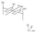
도 4를 참조하면, 메모리 셀 어레이(110)는 제 1 및 제 2 수직 워드라인들(VWL1, VWL2), 제 1 및 제 2 수평 워드라인들(HWL1, HWL2), 로컬 비트라인들(LBL1~LBL4), 및 3차원적으로 배열된 복수의 메모리 셀들(MC1, MC2)을 포함한다.Referring to FIG. 4, the
실시예들에 따르면, 메모리 셀 어레이(110)는 소정 개수의 메모리 셀들로 구성된 복수의 수직 셀 그룹들(VCG)을 포함할 수 있다. 수직 셀 그룹들(VCG) 각각은 제 1 수직 워드라인들(VWL1)과 로컬 비트라인들(LBL1~LBL4) 사이에 연결된 복수의 제 1 메모리 셀들(MC1)과, 제 2 수직 워드라인들(VWL2)과 로컬 비트라인들(LBL1~LBL4) 사이에 연결된 복수의 제 2 메모리 셀들(MC2)을 포함한다. 복수의 수직 셀 그룹들(VCG)은 제 2 방향(D2)으로 서로 이격되어 배열될 수 있으며, 각각의 수직 셀 그룹(VCG)에서 제 1 및 제 2 메모리 셀들(MC1, MC2)은 제 1 방향(D1) 및 제 3 방향(D3)으로 배열될 수 있다. 즉, 반도체 메모리 소자에서 복수의 수직 셀 그룹들(VCG)을 통해 제 1 및 제 2 메모리 셀들(MC1, MC2)이 3차원적으로 배열될 수 있다.According to embodiments, the
보다 상세하게, 수직 셀 그룹들(VCG) 각각은 제 1 방향(D1)으로 나란히 연장되며 제 3 방향(D3)으로 이격되어 배열된 복수의 로컬 비트라인들(LBL1~LBL4)과, 제 3 방향(D3)으로 나란히 연장되며 제 1 방향(D1)으로 이격되어 배열되는 복수의 제 1 수직 워드라인들(VWL1)을 포함한다. 이에 더하여, 수직 셀 그룹들(VCG) 각각은 제 3 방향(D3)으로 나란히 연장되며 제 1 방향(D1)으로 이격되어 배열되는 복수의 제 2 수직 워드라인들(VWL2)을 더 포함한다.More specifically, each of the vertical cell groups VCG includes a plurality of local bit lines LBL1 to LBL4 extending in the first direction D1 and spaced apart in the third direction D3, And a plurality of first vertical word lines (VWL1) extending in parallel to the first direction (D3) and arranged in a first direction (D1). In addition, each of the vertical cell groups VCG further includes a plurality of second vertical word lines VWL2 extending in the third direction D3 and arranged in the first direction D1.
하나의 수직 셀 그룹(VCG) 내에서, 로컬 비트라인들(LBL1~LBL4)은 제 1 및 제 2 방향(D1, D2)에 대해 수직인 제 3 방향(D3)으로 서로 이격되어 배열될 수 있다. 그리고, 제 1 수직 워드라인들(VWL1)은 로컬 비트라인들(LBL1~LBL4)의 제 1 측에 배치되며, 제 1 방향(D1)으로 서로 이격되어 배열될 수 있다. 제 2 수직 워드라인들(VWL2)은 로컬 비트라인들(LBL1~LBL4)의 제 2 측에서 제 1 방향(D1)으로 서로 이격되어 배열될 수 있다.In one vertical cell group VCG, the local bit lines LBL1 to LBL4 may be arranged apart from each other in a third direction D3 perpendicular to the first and second directions D1 and D2 . The first vertical word lines VWL1 are disposed on the first side of the local bit lines LBL1 to LBL4 and may be arranged apart from each other in the first direction D1. The second vertical word lines VWL2 may be arranged apart from each other in the first direction D1 on the second side of the local bit lines LBL1 to LBL4.
하나의 수직 셀 그룹(VCG) 내에서, 로컬 비트라인들(LBL1~LBL4)과 제 1 수직 워드라인들(VWL1)의 교차점들에 제 1 메모리 셀들(MC1)이 배치된다. 로컬 비트라인들(LBL1~LBL4)과 제 2 수직 워드라인들(VWL2)의 교차점들에 제 2 메모리 셀들(MC2)이 배치된다. 제 1 및 제 2 메모리 셀들(MC1, MC2)은 하나의 로컬 비트라인을 공유한다. 제 1 및 제 2 메모리 셀들(MC1, MC2)의 배열은 각 데이터 저장 요소에 접근하기 위한 선택 소자를 요구하지 않는 교점 메모리 어레이(cross point memory array)일 수 있다.In one vertical cell group VCG, the first memory cells MC1 are arranged at the intersections of the local bit lines LBL1 to LBL4 and the first vertical word lines VWL1. The second memory cells MC2 are disposed at the intersections of the local bit lines LBL1 to LBL4 and the second vertical word lines VWL2. The first and second memory cells MC1 and MC2 share one local bit line. The arrangement of the first and second memory cells MC1, MC2 may be a cross point memory array that does not require a selection element to access each data storage element.
실시예들에 따르면, 제 1 및 제 2 메모리 셀들(MC1, MC2) 각각은 하나의 저항성 메모리 요소(resistive memory element)로 구성될 수 있다. 저항성 메모리 요소는 그 양단에 인가되는 소정 전압에 의해서 가역적으로 명확하게 구별되는 적어도 두 가지 저항 상태 사이에서 스위칭되는 물질을 포함할 수 있다. 즉, 저항성 메모리 요소는 2가지의 안정한 저항성 상태(고저항 상태 및 저저항 상태)를 갖는 물질을 포함할 수 있다. 예를 들어, 저항성 메모리 요소는 페로브스카이트(perovskite) 화합물들, 전이 금속 산화물(transition metal oxide), 상변화 물질(phase-change material), 자성체 물질(magnetic materials), 강자성(ferromagnetic) 물질들 또는 반강자성(antiferromagnetic) 물질들을 포함할 수 있다.According to embodiments, each of the first and second memory cells MC1, MC2 may be configured with one resistive memory element. The resistive memory element may include a material that is switched between at least two resistive states that are clearly distinctly reversible by a predetermined voltage applied across the resistive memory element. That is, the resistive memory element may comprise a material having two stable resistive states (a high resistance state and a low resistance state). For example, the resistive memory element may include perovskite compounds, transition metal oxides, phase-change materials, magnetic materials, ferromagnetic materials, Or antiferromagnetic materials.
나아가, 실시예들에 따르면, 메모리 셀 어레이(110)는 제 2 방향(D2)으로 나란히 연장되며, 제 1 방향(D1)으로 이격되어 교대로 배열되는 제 1 및 제 2 수평 워드라인들(HWL1, HWL2)을 포함한다. 제 1 및 제 2 수평 워드라인들(HWL1, HWL2)은 복수의 수직 셀 그룹들(VCG)에 공통으로 연결될 수 있다. 또한, 제 1 및 제 2 수평 워드라인들(HWL1, HWL2)은 워드 라인 디코더(도 1의 2 참조)에 연결될 수 있다. 서로 다른 수직 셀 그룹들(VCG) 내의 제 1 수직 워드라인들(VWL1)이 하나의 제 1 수평 워드라인(HWL1)에 공통으로 연결될 수 있다. 서로 다른 수직 셀 그룹들(VCG) 내의 제 2 수직 워드라인들(VWL2)이 하나의 제 2 수평 워드라인(HWL2)에 공통으로 연결될 수 있다. 복수의 제 1 및 제 2 수평 워드라인들(HWL1, HWL2)은 서로 전기적으로 분리될 수 있다. 즉, 하나의 수직 셀 그룹(VCG)을 구성하는 제 1 및 제 2 수직 워드라인들(VWL1, VWL2)은 서로 전기적으로 분리될 수 있다.Further, according to embodiments, the
도 3 및 도 4를 참조하면, 복수의 수직 셀 그룹들(VCG) 각각은 수직 셀 그룹 선택부(120)와 연결될 수 있다. 상세하게, 수직 셀 그룹들(VCG) 각각의 로컬 비트라인들(LBL1~LBL4)은 수직 셀 그룹 선택부(120) 및 메모리 블록 선택부(130)에 의해 글로벌 비트라인들(GBL)에 각각 커플링된다. 복수의 수직 셀 그룹들(VCG)은 메모리 블록 선택부(130) 및 글로벌 비트라인들(GBL)을 공유할 수 있다. 글로벌 비트라인들(GBL)은 제 1 방향(D1)으로 나란히 연장될 수 있다. 글로벌 비트라인들(GBL)은 복수의 메모리 블록들(BLK)에 공통으로 연결될 수 있으며, 센스 앰프 및 페이지 버퍼(도 1의 5 참조)에 연결될 수 있다.Referring to FIG. 3 and FIG. 4, each of the plurality of vertical cell groups VCG may be connected to the vertical
수직 셀 그룹 선택부들(vertical string selection part; 120)은 도 3에 도시된 바와 같이, 메모리 셀 어레이(110)와 메모리 블록 선택부(130) 사이에 배치된다. 일 실시예에 따르면, 하나의 메모리 블록(BLK) 내에서 수직 셀 그룹 선택부(120)는 수직 셀 그룹들(VCG) 각각에 대응하여 배치된다. 수직 셀 그룹 선택부들(120)은 메모리 블록 선택부(130)를 수직 셀 그룹들(VCG) 중 어느 하나에 연결한다. 수직 셀 그룹 선택부들(120) 각각에 수직 선택 라인(VSL)이 연결된다. 수직 선택 라인들(VSL)은 제 1 방향(D1)으로 나란히 연장되며, 제 2 방향(D2)으로 서로 이격되어 배치될 수 있다. 수직 선택 라인들(VSL)은 복수의 메모리 블록들(BLK)에 공통으로 연결될 수 있으며, 수직 선택 라인 디코더(도 1의 4 참조)에 연결될 수 있다. 즉, 수직 셀 그룹 선택부들(120)은 수직 셀 그룹 선택 신호에 따라 수직 셀 그룹들(VCG) 중 어느 하나를 선택한다.The vertical
각각의 수직 셀 그룹 선택부(120)는 복수의 수직 셀 그룹 선택 트랜지스터들(VCST)을 포함한다. 수직 셀 그룹 선택 트랜지스터들(VCST)은 블록 선택 트랜지스터들(BST)과 로컬 비트라인들(LBL1~LBL4) 사이에 직렬 연결될 수 있다. 그리고, 수직 셀 그룹 선택 트랜지스터들(VCST)의 게이트 전극들은 수직 선택 라인(VSL)에 공통으로 연결될 수 있다.Each vertical cell
메모리 블록 선택부(130)는 글로벌 비트 라인들(GBL)과 수직 셀 그룹 선택부들(120) 사이에 배치된다. 각 메모리 블록들(BLK) 내에서 복수의 수직 셀 그룹 선택부들(120)은 하나의 메모리 블록 선택부(130)를 공유한다.The
메모리 블록 선택부(130)는 글로벌 비트라인들(GBL)을 수직 셀 그룹 선택부들(120) 중 어느 하나와 연결한다. 메모리 블록 선택부(130)는 글로벌 비트라인들(GBL) 각각에 대응되는 복수의 블록 선택 트랜지스터들(BST)을 포함한다. 블록 선택 트랜지스터들(BST) 각각은 수직 셀 그룹 선택 트랜지스터(VCST)와 직렬 연결된다. 블록 선택 트랜지스터들(BST)의 게이트 전극들은 블록 선택 라인(BSL)에 공통으로 연결된다. 메모리 블록 선택부(130)는 블록 선택 라인 디코더(도 1의 1 참조)와 연결된 블록 선택 라인(BSL)에 의해 동작이 제어된다.The memory
도 5는 본 발명의 실시예들에 따른 반도체 메모리 장치에서 메모리 셀 어레이의 일부를 나타내는 회로도이다. 도 6는 본 발명의 실시예들에 따른 반도체 메모리 장치에서 메모리 셀 어레이의 일부를 나타내는 평면도이다.5 is a circuit diagram showing a part of a memory cell array in a semiconductor memory device according to embodiments of the present invention. 6 is a plan view showing a part of a memory cell array in a semiconductor memory device according to embodiments of the present invention.
도 5 및 도 6을 참조하면, 본 발명의 실시예들에 따른 메모리 셀 어레이(110)에서, 수직 셀 그룹들(VCG) 각각은 제 1 및 제 2 메모리 셀들(MC1, MC2)을 포함한다. 제 1 메모리 셀(MC1)은 제 1 방향(D1)으로 연장되는 로컬 비트라인(LBL)과, 로컬 비트라인(LBL)을 가로지르며 제 3 방향(D3)으로 연장되는 제 1 수직 워드라인(VWL1), 및 로컬 비트 라인(LBL)과 제 1 수직 워드라인(VWL1) 사이의 데이터 저장 요소(DS)로 구성된다. 제 2 메모리 셀(MC2)은 제 1 방향(D1)으로 연장되는 로컬 비트라인(LBL), 제 1 수직 워드라인(VWL1)과 평행하되 제 2 방향(D2)으로 이격된 제 2 수직 워드라인(VWL2), 및 로컬 비트라인(LBL)과 제 2 수직 워드라인(VWL2) 사이의 데이터 저장 요소(DS)로 구성될 수 있다. 그리고, 본 발명의 실시예들에 따른 메모리 셀 어레이(110)에서, 제 1 수직 워드라인(VWL1)과 제 2 수직 워드라인(VWL2)은 전기적으로 분리되며, 이에 따라, 제 1 및 제 2 메모리 셀들(MC1, MC2)은 각각 독립적으로 선택될 수 있다. 그리고, 제 1 및 제 2 메모리 셀들(MC1, MC2)은 로컬 비트라인(LBL)을 공유한다. 이러한 제 1 및 제 2 메모리 셀들(MC1, MC2)은, 도 4를 참조하여 설명한 수직 셀 그룹들(VCG)을 통해 3차원적 구조로 배열된다. 그러므로 반도체 메모리 장치의 집적도가 보다 증가될 수 있다.Referring to FIGS. 5 and 6, in the
이하, 도 3 및 도 7을 참조하여, 본 발명의 실시예들에 따른 반도체 메모리 장치에서 메모리 셀을 선택하는 방법에 대해 설명한다.Hereinafter, with reference to FIG. 3 and FIG. 7, a method of selecting a memory cell in the semiconductor memory device according to the embodiments of the present invention will be described.
도 7은 본 발명의 실시예들에 따른 반도체 메모리 장치에서 하나의 메모리 셀을 선택하는 방법을 설명하기 위한 개략 회로도이다.7 is a schematic circuit diagram for explaining a method of selecting one memory cell in a semiconductor memory device according to embodiments of the present invention.
본 발명의 실시예들에 따르면, 블록 선택 라인 디코더(도 1의 1 참조)에서 제공된 블록 선택 신호에 의해, 복수의 메모리 블록들(BLK) 중 어느 하나가 선택될 수 있다. 즉, 도 3을 참조하면, 선택된 메모리 블록(BLK)의 블록 선택 라인(BSL)에 턴온(turn on) 전압이 인가될 수 있다. 이에 따라, 선택된 메모리 블록(BLK)의 블록 선택 트랜지스터들(BST)이 턴온(turn on)되어 글로벌 비트 라인들(GBL)이 수직 셀 그룹 선택부들(120)과 연결될 수 있다.According to the embodiments of the present invention, any one of the plurality of memory blocks BLK can be selected by the block selection signal provided in the block selection line decoder (see 1 in FIG. 1). That is, referring to FIG. 3, a turn-on voltage may be applied to the block select line BSL of the selected memory block BLK. Accordingly, the block selection transistors BST of the selected memory block BLK may be turned on so that the global bit lines GBL may be connected to the vertical
도 3 및 도 7을 참조하면, 선택된 메모리 블록(BLK) 내에서, 선택하고자 하는 메모리 셀(MC_SEL)을 포함하는 수직 셀 그룹(VCG_SEL)을 선택한다. 즉, 수직 선택 라인들(VSL) 중 어느 하나에 턴온 전압이 인가되어, 수직 셀 그룹 선택부들(120) 중 어느 하나가 선택될 수 있다. 이에 따라, 선택된 수직 셀 그룹 선택부(120)의 수직 셀 그룹 선택 트랜지스터들(VCST)이 턴온되어, 선택된 수직 셀 그룹(VCG_SEL)의 로컬 비트라인들(LBL)과 글로벌 비트 라인들(GBL)이 전기적으로 연결될 수 있다.3 and 7, in the selected memory block BLK, the vertical cell group VCG_SEL including the memory cell MC_SEL to be selected is selected. That is, any one of the vertical
이어서, 제 1 및 제 2 수평 워드라인들(HWL1, HWL2) 중 선택된 어느 하나와, 로컬 비트라인들(LBL1~LBL4) 중 선택된 어느 하나에 동작 전압을 인가함에 따라, 선택된 수직 셀 그룹(VCG_SEL) 내에서 로컬 비트라인(LBL3_SEL)을 공유하는 제 1 및 제 2 메모리 셀들(MC1, MC2) 중 하나가 선택될 수 있다.Subsequently, the selected vertical cell group VCG_SEL is selected by applying an operation voltage to any one of the selected one of the first and second horizontal word lines HWL1 and HWL2 and the selected one of the local bit lines LBL1 to LBL4, One of the first and second memory cells MC1 and MC2 sharing the local bit line LBL3_SEL may be selected.
보다 상세하게, 글로벌 비트라인들(GBL) 중에서 선택된 글로벌 비트라인에 동작 전압(읽기 전압, 쓰기 전압, 소거 전압)이 인가될 수 있다. 선택된 수직 셀 그룹(VCG_SEL)에서, 선택된 글로벌 비트라인과 연결된 로컬 비트라인(LBL3_SEL)에 동작 전압이 인가될 수 있다. 그리고, 수평 워드라인들(HWL1, HWL2) 중에서 선택된 수평 워드라인(HWL1_SEL)에 동작 전압(읽기 전압, 쓰기 전압(셋 또는 리셋 전압), 소거 전압)이 인가될 수 있다. 이에 따라, 선택된 수평 워드라인(HWL1_SEL)에 접속된 복수의 수직 워드라인들(VWL1)에 동작 전압이 인가될 수 있다.More specifically, an operation voltage (a read voltage, a write voltage, and an erase voltage) may be applied to a global bit line selected from the global bit lines GBL. In the selected vertical cell group VCG_SEL, the operation voltage may be applied to the local bit line LBL3_SEL connected to the selected global bit line. An operation voltage (a read voltage, a write voltage (set or reset voltage), and an erase voltage) may be applied to the horizontal word line HWL1_SEL selected from the horizontal word lines HWL1 and HWL2. Accordingly, an operation voltage can be applied to a plurality of vertical word lines (VWL1) connected to the selected horizontal word line (HWL1_SEL).
여기서, 선택된 수평 워드라인(HWL1_SEL)에 인가되는 워드라인 전압과 선택된 로컬 비트라인(LBL3_SEL)에 인가되는 비트라인 전압 간의 전압 차이가, 비선택된 워드 라인에 인가되는 워드라인 전압과 비선택된 비트라인에 인가되는 전압 간의 전압차이보다 클 수 있다. 그리고, 선택된 수평 워드라인(HWL1_SEL)에 인가되는 워드라인 전압은 선택된 로컬 비트라인(LBL3_SEL)에 인가되는 비트라인 전압보다 크거나 작을 수 있다. 이와 같이, 선택된 수평 워드라인(HWL1_SEL)과 선택된 로컬 비트라인(LBL3_SEL) 사이의 전압 차이에 의해 선택된 메모리 셀(MC_SEL)의 저항성 메모리 요소는 저항성 상태가 가역적으로 스위칭될 수 있다. 나아가, 선택된 메모리 셀(MC_SEL)의 저항성 메모리 요소가 셋(Set) 상태(데이터 1이 저장된 상태 또는 ON 상태) 또는 리셋(reset) 상태(데이터 0이 저장된 상태 또는 OFF 상태)을 갖도록 수평 워드라인(HWL1_SEL)과 선택된 로컬 비트라인(LBL3_SEL) 사이의 전압 차이가 조절될 수 있다.Here, the voltage difference between the word line voltage applied to the selected horizontal word line HWL1_SEL and the bit line voltage applied to the selected local bit line LBL3_SEL is different from the word line voltage applied to the unselected word line May be greater than the voltage difference between the applied voltages. The word line voltage applied to the selected horizontal word line HWL1_SEL may be larger or smaller than the bit line voltage applied to the selected local bit line LBL3_SEL. In this manner, the resistive memory element of the memory cell MC_SEL selected by the voltage difference between the selected horizontal word line HWL1_SEL and the selected local bit line LBL3_SEL can be reversibly switched in its resistive state. Further, the horizontal word line (or the data word) is set so that the resistive memory element of the selected memory cell MC_SEL has a Set state (data 1 is stored or ON) or a reset (data 0 is stored or OFF) HWL1_SEL) and the selected local bit line LBL3_SEL can be adjusted.
실시예들에 따르면, 선택된 수직 셀 그룹(VCG_SEL)에서 선택된 로컬 비트라인(LBL3_SEL)을 공유하는 제 1 및 제 2 메모리 셀들(MC1, MC2)은 서로 다른 수직 워드라인들(VWL1, VWL2)에 연결되어 있으므로, 선택된 수직 워드라인(VWL1_SEL)과 선택된 로컬 비트라인(LBL3_SEL)에 의해 제 1 및 제 2 메모리 셀들(MC1, MC2) 중 하나가 선택될 수 있다.The first and second memory cells MC1 and MC2 sharing the local bit line LBL3_SEL selected in the selected vertical cell group VCG_SEL are connected to the different vertical word lines VWL1 and VWL2 , One of the first and second memory cells MC1 and MC2 can be selected by the selected vertical word line VWL1_SEL and the selected local bit line LBL3_SEL.
도 8a는 본 발명의 제 1 실시예에 따른 메모리 셀 어레이를 나타내는 사시도이다. 도 8b는 도 8a에 도시된 메모리 셀 어레이의 평면도이다. 도 8c는 도 8a에 도시된 메모리 셀 어레이의 단면도로서, 도 8b의 I-I'선을 따라 자른 단면이다.8A is a perspective view showing a memory cell array according to the first embodiment of the present invention. 8B is a plan view of the memory cell array shown in FIG. 8A. 8C is a cross-sectional view of the memory cell array shown in FIG. 8A, taken along the line I-I 'in FIG. 8B.
도 8a, 도 8b 및 도 8c를 참조하면, 기판(100)은 반도체 특성을 갖는 물질(예를 들면, 실리콘 웨이퍼), 절연성 물질(예를 들면, 유리), 절연성 물질에 의해 덮인 반도체 또는 도전체 중의 하나일 수 있다.8A, 8B and 8C, the
기판(100) 상에는 복수의 로컬 비트라인 구조체들(LBLS)이 배치될 수 있다. 일 실시예에서, 로컬 비트라인 구조체들(LBLS)은 기판(100) 상면을 덮는 절연막(101) 상에 배치될 수 있다.A plurality of local bit line structures (LBLS) may be disposed on the substrate (100). In one embodiment, the local bit line structures (LBLS) may be disposed on the insulating
실시예들에 따르면, 로컬 비트라인 구조체들(LBLS)은 제 1 방향(D1)으로 연장되며, 제 2 방향(D2)으로 서로 이격되어 배치될 수 있다. 로컬 비트라인 구조체들(LBLS) 각각은 서로 대향하는 제 1 측벽과 제 2 측벽을 가질 수 있다. 각각의 로컬 비트라인 구조체들(LBLS)은 층간 절연막들(105)을 개재하여 제 3 방향(D3)으로 적층된 복수의 로컬 비트라인들(LBL1~LBL4)을 포함한다. 즉, 제 1 방향(D1)으로 연장되는 로컬 비트라인들(LBL1~LBL4)이 기판(100) 상에 수직적으로 적층될 수 있다. 수직적으로 인접하는 로컬 비트라인들(LBL1~LBL4)은 층간 절연막들(105)에 의해 서로 전기적으로 분리될 수 있다. 로컬 비트라인들(LBL1~LBL4)은 도전 물질로 이루어질 수 있으며, 예를 들어, 불순물이 도핑된 반도체 물질(ex, 실리콘, 게르마늄 또는 실리콘-게르마늄 등), 도전성 금속질화물(ex, 질화티타늄 또는 질화탄탈늄 등), 금속실리사이드(ex, 텅스텐실리사이드, 코발트실리사이드 등) 및 금속(ex, 티타늄, 탄탈늄, 텅스텐, 알루미늄 등) 중에서 선택된 적어도 하나를 포함할 수 있다.According to embodiments, the local bit line structures LBLS extend in a first direction D1 and may be spaced apart from each other in a second direction D2. Each of the local bit line structures (LBLS) may have first and second sidewalls facing each other. Each of the local bit line structures LBLS includes a plurality of local bit lines LBL1 to LBL4 stacked in the third direction D3 via the
실시예들에 따르면, 로컬 비트라인 구조체들(LBLS)의 제 1 측벽에 로컬 비트라인들(LBL1~LBL4)을 가로지르는 제 1 수직 워드라인들(VWL1)이 배치될 수 있다. 제 1 수직 워드라인들(VWL1)은 기판(100)의 상면에 대해 실질적으로 수직하며, 제 1 방향(D1)으로 서로 이격되어 배치된다. 로컬 비트라인 구조체들(LBLS)의 제 2 측벽에 로컬 비트라인들(LBL1~LBL4)을 가로지르는 제 2 수직 워드라인들(VWL2)이 배치될 수 있다. 제 2 수직 워드라인들(VWL2)은 기판(100)의 상면에 대해 실질적으로 수직하며, 제 1 방향(D1)으로 서로 이격되어 배치된다.According to embodiments, first vertical word lines VWL1 may be disposed across the local bit lines LBL1 to LBL4 on the first sidewall of the local bit line structures LBLS. The first vertical word lines VWL1 are substantially perpendicular to the upper surface of the
이 실시예에 따르면, 제 1 수직 워드라인들(VWL1)과 제 2 수직 워드라인들(VWL2)은, 도 8a 및 도 8b에 도시된 바와 같이, 평면적 관점에서 제 2 방향(D2)으로 번갈아 배치될 수 있다. 다시 말해, 평면적 관점에서, 로컬 비트라인 구조체(LBLS)를 사이에 두고 제 1 및 제 2 수직 워드라인들(VWL1, VWL2)이 서로 대향할 수 있다. 이에 더하여, 제 2 수직 워드라인들(VWL2)은 제 1 수직 워드라인들(VWL1)에 대해 사선 방향에 배치될 수 있다.According to this embodiment, the first vertical word lines VWL1 and the second vertical word lines VWL2 are arranged alternately in the second direction D2 from the plan view, as shown in Figs. 8A and 8B . In other words, in a plan view, the first and second vertical word lines VWL1 and VWL2 can face each other with the local bit line structure LBLS therebetween. In addition, the second vertical word lines VWL2 may be arranged diagonally with respect to the first vertical word lines VWL1.
나아가, 이 실시예에 따르면, 제 1 및 제 2 수직 워드라인들(VWL1, VWL2)은 로컬 비트라인 구조체(LBLS)의 제 1 측벽과 인접한 일측벽과, 다른 로컬 비트라인 구조체(LBLS)의 제 2 측벽에 인접한 타측벽을 가질 수 있다. 다시 말해, 제 2 방향(D2)에서 제 1 및 제 2 수직 워드라인들(VWL1, VWL2) 각각의 폭은 인접하는 로컬 비트라인 구조체들(LBLS) 간의 간격의 1/2 이상일 수 있다.Further, according to this embodiment, the first and second vertical word lines VWL1 and VWL2 are connected to one side wall adjacent to the first sidewall of the local bit line structure LBLS and the other side wall of the other local bit line structure LBLS Lt; RTI ID = 0.0 > 2 < / RTI > In other words, the width of each of the first and second vertical word lines (VWL1, VWL2) in the second direction (D2) may be more than half of the interval between the adjacent local bit line structures (LBLS).
이 실시예에 따르면, 로컬 비트라인 구조체들(LBLS) 상에 로컬 비트라인들(LBL1~LBL4)을 가로지르는 복수의 제 1 수평 워드라인들(HWL1)과 복수의 제 2 수평 워드라인들(HWL2)이 배치될 수 있다. 상세하게, 제 1 및 제 2 수평 워드라인들(HWL1, HWL2)은 제 2 방향(D2)으로 나란히 연장되며, 제 1 방향(D1)으로 이격되어 배치된다. 평면적 관점에서, 제 2 수평 워드라인(HWL2)은 인접하는 제 1 수평 워드라인들(HWL1) 사이에 배치된다. 즉, 제 1 및 제 2 수평 워드라인들(HWL1, HWL2)은 제 1 방향(D1)으로 번갈아 배치된다.According to this embodiment, a plurality of first horizontal word lines (HWL1) and a plurality of second horizontal word lines (HWL2), which cross local bit lines (LBL1 to LBL4), are formed on local bit line structures (LBLS) May be disposed. In detail, the first and second horizontal word lines HWL1 and HWL2 extend in the second direction D2 and are disposed apart from each other in the first direction D1. From a plan viewpoint, the second horizontal word line HWL2 is disposed between adjacent first horizontal word lines HWL1. That is, the first and second horizontal word lines HWL1 and HWL2 are alternately arranged in the first direction D1.
실시예들에 따르면, 제 1 수평 워드라인들(HWL1)의 수는 하나의 로컬 비트라인 구조체(LBLS)를 구성하는 로컬 비트라인들(LBL1~LBL4)의 수와 동일할 수 있다. 즉, 제 1 수평 워드라인들(HWL1)의 수는 기판(100) 상에 적층된 로컬 비트라인들(LBL1~LBL4)의 적층수와 동일할 수 있다. 마찬가지로, 제 2 수평 워드라인들(HWL2)의 수는 하나의 로컬 비트라인 구조체(LBLS)를 구성하는 로컬 비트라인들(LBL1~LBL4)의 수와 동일할 수 있다. 나아가, 제 1 수평 워드라인들(HWL1)은 제 2 방향(D2)에서 인접하는 제 1 수직 워드라인들(VWL1)과 제 1 콘택 플러그들(CPL1)을 통해 공통으로 접속될 수 있다. 그리고, 제 2 수평 워드라인들(HWL2)은 제 2 방향(D2)에서 인접하는 제 2 수직 워드라인들(VWL2)과 제 2 콘택 플러그들(CPL2)을 통해 공통으로 접속될 수 있다.According to the embodiments, the number of first horizontal word lines HWL1 may be equal to the number of local bit lines LBL1 to LBL4 constituting one local bit line structure LBLS. That is, the number of the first horizontal word lines HWL1 may be equal to the number of stacked local bit lines LBL1 to LBL4 stacked on the
제 1 수평 워드라인들(HWL1)과 제 2 수평 워드라인들(HWL2)은 기판(100)의 상면으로부터 다른 수직적 거리에 배치될 수 있다. 이 실시예에서, 복수의 제 1 및 제 2 수평 워드라인들(HWL1, HWL2)은 서로 전기적으로 분리될 수 있다. 즉, 이에 따라, 제 1 수직 워드라인(VWL1)과 제 2 수직 워드라인(VWL2)은 전기적으로 분리된다. 이 실시예에 따르면, 수직적 관점에서 제 1 수평 워드라인들(HWL1)은 로컬 비트라인 구조체(LBLS)의 상부면과 제 2 수평 워드라인들(HWL2) 사이에 배치될 수 있다.The first horizontal word lines HWL1 and the second horizontal word lines HWL2 may be arranged at different vertical distances from the upper surface of the
실시예들에 따르면, 로컬 비트라인들(LBL1~LBL4)과 제 1 및 제 2 수직 워드라인들(VWL1, VWL2) 사이에 데이터 저장막(DSL)이 개재될 수 있다. 데이터 저장막(DSL)은 로컬 비트라인 구조체들(LBLS)의 제 1 및 제 2 측벽들과 상부면들을 덮을 수 있다. 데이터 저장막(DSL)은 그 양단에 인가된 소정 전압에 의해서 가역적으로 명확하게 구별되는 적어도 두 가지 저항 상태 사이에서 스위칭되는 물질로 형성될 수 있다. 예를 들어, 데이터 저장막(DSL)은 페로브스카이트 결정상을 나타내는 절연물질, MOx로 표시되는 절연성 금속 산화물, 또는 이들의 조합으로 이루어진다. 페로브스카이트 결정상을 나타내는 절연 물질은 이른바 ABO3 구조를 가지는 절연물질로서, 특별히 여기에 한정되는 것은 아니며, PbZrTiO3, PrCaMnO3, 칼슘이 도핑된 (Ba, Sr)TiO3, SrZrO3 등을 포함한다. 절연성 금속 산화물 MOx 에서 M은 금속을 가리키며 금속(M)은 전이 금속을 포함한다. 즉, 절연성 금속 산화물(MOx)은 전이금속 산화물 또는 귀금속 산화물이다. 예를 들어, 전이금속으로 특별히 여기에 한정되는 것은 아니며 니켈(Ni), 니오븀(Nb), 티타늄(Ti), 지르코늄(Zr), 하프늄(Hf), 코발트(Co), 철(Fe), 구리(Cu), 망간(Mn), 크롬(Cr) 등을 포함한다. 전이금속 산화물 또한 리튬, 칼슘, 또는 란타늄 같은 불순물을 함유할 수 있다. 이와 달리, 데이터 저장막(DSL)은 공급되는 열의 온도 및/또는 공급 시간 등에 따라 비저항이 변경되는 상변화 물질을 포함할 수 있다. 예를 들어, 데이터 저장막(DSL)은 칼코게나이드(chalcogenide)계 원소인 Te 및 Se 중의 적어도 하나와, Ge, Sb, Bi, Pb, Sn, Ag, As, S, Si, P, O 및 N 중에서 선택된 적어도 하나를 포함하는 화합물로 형성될 수 있다. 또 다른 예로, 데이터 저장막(DSL)은 자유층 및 고정층간의 자화방향에 따라 저항값이 변경되는 자기터널접합체(MTJ)를 포함할 수도 있다.According to the embodiments, a data storage film (DSL) may be interposed between the local bit lines LBL1 to LBL4 and the first and second vertical word lines VWL1 and VWL2. The data storage layer (DSL) may cover the first and second sidewalls and upper surfaces of the local bit line structures (LBLS). The data storage film (DSL) may be formed of a material that is switched between at least two resistance states which are clearly distinguishable reversibly by a predetermined voltage applied across the data storage film (DSL). For example, the data storage layer (DSL) may be formed of an insulating material representing a perovskite crystal phase, an insulating metal oxide represented by MOx, or a combination thereof. The insulating material exhibiting the perovskite crystal phase is an insulating material having a so-called ABO3 structure, and is not particularly limited thereto. Examples of the insulating material include PbZrTiO3 , PrCaMnO3 , calcium-doped (Ba, Sr) TiO3 , SrZrO3 , . In the insulating metal oxide MOx, M denotes a metal, and the metal (M) includes a transition metal. That is, the insulating metal oxide (MOx) is a transition metal oxide or a noble metal oxide. Examples of the transition metal include, but are not limited to, nickel, niobium, titanium, zirconium, hafnium, cobalt, iron, copper, (Cu), manganese (Mn), chromium (Cr), and the like. The transition metal oxide may also contain impurities such as lithium, calcium, or lanthanum. Alternatively, the data storage layer (DSL) may include a phase change material whose specific resistance changes depending on the temperature and / or the supply time of the supplied heat. For example, the data storage layer (DSL) may include at least one of Te and Se, chalcogenide-based elements, Ge, Sb, Bi, Pb, Sn, Ag, As, S, Si, P, N < / RTI > As another example, the data storage layer (DSL) may include a magnetic tunnel junction (MTJ) whose resistance value changes according to the magnetization direction between the free layer and the pinned layer.
도 9a는 본 발명의 제 2 실시예에 따른 메모리 셀 어레이를 나타내는 사시도이다. 도 9b는 도 9a에 도시된 메모리 셀 어레이의 평면도이다. 도 9c는 도 9a에 도시된 메모리 셀 어레이의 단면도로서, 도 9b의 I-I' 선을 따라 자른 단면이다.9A is a perspective view showing a memory cell array according to a second embodiment of the present invention. FIG. 9B is a plan view of the memory cell array shown in FIG. 9A. FIG. 9C is a cross-sectional view of the memory cell array shown in FIG. 9A, taken along the line I-I 'in FIG. 9B.
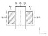
도 9a, 도 9b 및 도 9c에 도시된 반도체 메모리 장치에서, 도 8a, 도 8b 및 도 8c에 도시된 실시예와 실질적으로 동일한 구성 요소에 대해서는 동일한 도면 부호를 사용하며, 해당 구성 요소에 대한 상세한 설명은 생략하기로 한다.In the semiconductor memory device shown in Figs. 9A, 9B and 9C, the same reference numerals are used for components substantially the same as the embodiments shown in Figs. 8A, 8B and 8C, A description thereof will be omitted.
도 9a, 도 9b 및 도 9c를 참조하면, 로컬 비트라인 구조체들(LBLS)이 제 2 방향(D2)으로 서로 이격되어 기판(100) 상에 배치된다. 제 1 수직 워드라인들(VWL1)이 로컬 비트라인 구조체들(LBLS)의 제 1 측벽들에 배치되며, 제 2 수직 워드라인들(VWL2)이 로컬 비트라인 구조체들(LBLS)의 제 2 측벽들에 제 1 수직 워드라인들(VWL1)과 대향하여 배치될 수 있다. 즉, 로컬 비트라인 구조체(LBLS)를 사이에 두고, 제 1 수직 워드라인(VWL1)과 제 2 수직 워드라인(VWL2)이 서로 마주보도록 배치될 수 있다. 나아가, 이 실시예에 따르면, 인접하는 로컬 비트라인 구조체들(LBLS) 사이에 제 1 수직 워드라인(VWL1)과 제 2 수직 워드라인(VWL2)이 서로 이격되어 배치될 수 있다. 다시 말해, 제 2 방향(D2)에서 제 1 및 제 2 수직 워드라인들(VWL1, VWL2) 각각의 폭은 인접하는 로컬 비트라인 구조체들(LBLS) 간의 간격의 1/2 이하일 수 있다. 각각의 제 1 수직 워드라인들(VWL1) 상에 제 1 콘택 플러그(CPL1)가 배치되며, 각각의 제 2 수직 워드라인들(VWL2) 상에 제 2 콘택 플러그(CPL2)가 배치될 수 있다. 이 실시예에서, 제 1 및 제 2 콘택 플러그들(CPL1, CPL2)은 제 2 방향(D2)으로 따라 번갈아 배열되어 하나의 행을 이룰 수 있다.9A, 9B, and 9C, local bit line structures LBLS are disposed on the
복수의 로컬 비트라인 구조체들(LBLS) 상에 제 1 및 제 2 수평 워드라인들(HWL1, HWL2)이 배치될 수 있다. 제 1 수평 워드라인들(HWL1)과 제 2 수평 워드라인들(HWL2)은 기판(100)으로부터 서로 다른 수직적 거리에 배치될 수 있다. 이 실시예에 따르면, 수직적 관점에서, 제 1 수평 워드라인들(HWL1)은 로컬 비트라인 구조체들(LBLS)과 제 2 수평 워드라인들(HWL2) 사이에 배치될 수 있다. 그리고, 평면적 관점에서, 제 1 수평 워드라인들(HWL1)은 로컬 비트라인들(LBL1~LBL4)을 가로지르는 배선부와, 배선부에서 제 2 방향(D2)으로 돌출되어 제 1 콘택 플러그들(CPL1)과 접속되는 콘택부를 포함할 수 있다. 제 2 수평 워드라인들(HWL2)은 평면적 관점에서 제 1 수평 워드라인들(HWL1)의 배선부들 사이에서 제 2 콘택 플러그들(CPL2)과 접속될 수 있다.The first and second horizontal word lines HWL1 and HWL2 may be disposed on the plurality of local bit line structures LBLS. The first horizontal word lines HWL1 and the second horizontal word lines HWL2 may be arranged at different vertical distances from the
도 10a는 본 발명의 제 3 실시예에 따른 메모리 셀 어레이(110)를 나타내는 사시도이다. 도 10b는 도 10a에 도시된 메모리 셀 어레이(110)의 평면도이다. 도 10c는 도 10a에 도시된 메모리 셀 어레이(110)의 단면도로서, 도 10b의 I-I'선을 따라 자른 단면이다.10A is a perspective view showing a
도 10a, 도 10b 및 도 10c에 도시된 반도체 메모리 장치에서, 도 8a, 도 8b 및 도 8c에 도시된 실시예와 실질적으로 동일한 구성 요소에 대해서는 동일한 도면 부호를 사용하며, 해당 구성 요소에 대한 상세한 설명은 생략하기로 한다.In the semiconductor memory device shown in Figs. 10A, 10B, and 10C, the same reference numerals are used for components substantially the same as the embodiments shown in Figs. 8A, 8B, and 8C, A description thereof will be omitted.
도 10a, 도 10b, 및 도 10c를 참조하면, 로컬 비트라인 구조체들(LBLS)이 제 2 방향(D2)으로 서로 이격되어 기판(100) 상에 배치된다. 제 1 수직 워드라인들(VWL1)이 로컬 비트라인 구조체들(LBLS)의 제 1 측벽들에 배치되며, 제 2 수직 워드라인들(VWL2)이 로컬 비트라인 구조체들(LBLS)의 제 2 측벽들에 제 1 수직 워드라인들(VWL1)과 대향하여 배치될 수 있다. 즉, 로컬 비트라인 구조체(LBLS)를 사이에 두고, 제 1 수직 워드라인(VWL1)과 제 2 수직 워드라인(VWL2)이 서로 마주보도록 배치될 수 있다. 그리고, 이 실시예에 따르면, 인접하는 로컬 비트라인 구조체들(LBLS) 사이에 제 1 수직 워드라인(VWL1)과 제 2 수직 워드라인(VWL2)이 배치될 수 있다.10A, 10B, and 10C, the local bit line structures LBLS are disposed on the
이 실시예에 따르면, 수직적 관점에서, 기판(100)과 복수의 로컬 비트라인 구조체들(LBLS) 사이에 제 1 수평 워드라인들(HWL1)이 배치되며, 복수의 로컬 비트라인 구조체들(LBLS) 상에 제 2 수평 워드라인들(HWL2)이 배치될 수 있다. 제 1 및 제 2 수평 워드라인들(HWL1, HWL2)은 복수의 로컬 비트라인 구조체들(LBLS)과 절연된다.According to this embodiment, in a vertical view, first horizontal word lines HWL1 are disposed between a
제 1 수평 워드라인들(HWL1)은 기판(100)의 절연막(101) 상에서 로컬 비트라인들(LBL1~LBL4)을 가로지르는 방향(즉, 제 2 방향(D2))으로 나란히 연장되어 배치될 수 있다. 제 1 수평 워드라인(HWL1) 각각에 제 2 방향(D2)에서 인접하는 제 1 수직 워드라인들(VWL1)이 공통으로 접속될 수 있다. 즉, 제 1 수직 워드라인들(VWL1)은 제 1 수평 워드라인(HWL1) 상에서 제 3 방향(D3)으로 연장될 수 있다.The first horizontal word lines HWL1 may be arranged extending in parallel in the direction (that is, the second direction D2) across the local bit lines LBL1 to LBL4 on the insulating
제 2 수평 워드라인들(HWL2)은 로컬 비트라인들(LBL1~LBL4)을 가로지르는 방향(즉, 제 2 방향(D2))으로 나란히 연장되어 배치되며, 평면적 관점에서, 제 1 수평 워드라인들(HWL1)과 중첩될 수 있다. 제 2 수평 워드라인들(HWL2) 각각은 제 2 방향(D2)에서 인접하는 제 2 수직 워드라인들(VWL2)과 공통으로 접속될 수 있다.The second horizontal word lines HWL2 are arranged extending in a direction transverse to the local bit lines LBL1 through LBL4 (i.e., in the second direction D2), and in plan view, (HWL1). Each of the second horizontal word lines HWL2 may be connected in common with the adjacent second vertical word lines VWL2 in the second direction D2.
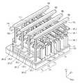
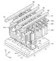
도 11은 본 발명의 제 1 실시예에 따른 반도체 메모리 장치의 메모리 블록을 나타내는 사시도이다. 도 12는 도 11에 도시된 메모리 블록의 수직 셀 그룹 선택부를 설명하기 위한 사시도이다. 도 13 및 도 14는 본 발명의 실시예들에 따른 반도체 메모리 장치에서, 적층된 배선 패턴들의 패드 구조를 설명하기 위한 사시도 및 평면도이다.11 is a perspective view showing a memory block of the semiconductor memory device according to the first embodiment of the present invention. 12 is a perspective view for explaining a vertical cell group selection unit of the memory block shown in FIG. 13 and 14 are a perspective view and a plan view for explaining the pad structure of the stacked wiring patterns in the semiconductor memory device according to the embodiments of the present invention.
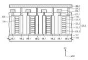
도 11 내지 도 14를 참조하면, 기판(100)은 셀 어레이 영역(10) 및 주변 회로 영역(20)을 포함한다. 그리고, 주변 회로 영역(20)은 수직 셀 그룹 선택 영역(21), 블록 선택 영역(25), 및 이들 사이의 콘택 영역(23)을 포함한다.Referring to Figs. 11 to 14, the
셀 어레이 영역(10)의 기판(100) 상에 본 발명의 실시예들에 따른 메모리 셀 어레이(110)가 배치된다. 즉, 도 8a 내지 도 8c, 도 9a 내지 도 9c 및 도 10a 내지 도 10c에 도시된 메모리 셀 어레이(110)들 중 어느 하나가 형성될 수 있다. 다시 말해, 셀 어레이 영역(10)의 기판(100) 상에 제 1 방향(D1)으로 연장되는 복수의 로컬 비트라인 구조체들(LBLS)이 배치되며, 로컬 비트라인 구조체들(LBLS) 양측에 제 1 및 제 2 수직 워드라인들(VWL1, VWL2)이 배치된다. 그리고, 로컬 비트라인 구조체들(LBLS) 상에 로컬 비트라인들(LBL1~LBL4)을 가로지르는 제 1 및 제 2 수평 워드라인들(HWL1, HWL2)이 배치될 수 있다. 제 1 및 제 2 수평 워드라인들(HWL1, HWL2)은 기판(100)으로부터 서로 다른 수직적 높이에 배치될 수 있다.On the
도 11 및 도 12를 참조하면, 수직 셀 그룹 선택 영역(21)의 기판(100) 상에 수직 셀 그룹 선택부들(도 3의 120 참조)이 배치될 수 있다. 수직 셀 그룹 선택부들(도 3의 120 참조) 각각은 복수의 수직 셀 그룹 선택 트랜지스터들(도 3의 VCST 참조)을 포함한다. 하나의 수직 셀 그룹 선택부(도 3의 120 참조)는 하나의 로컬 비트라인 구조체(LBLS)와 이것 양측의 수직 선택 게이트 전극들(VSG)로 구성될 수 있다. 즉, 수직적으로 적층된 로컬 비트라인들(LBL1~LBL4)과 수직 선택 게이트 전극들(VSG)에 의해 복수의 수직 셀 그룹 선택 트랜지스터들(도 3의 VCST 참조)이 구성될 수 있다.Referring to FIGS. 11 and 12, vertical cell group selectors (see 120 in FIG. 3) may be disposed on the
실시예들에 따르면, 로컬 비트라인 구조체들(LBLS)은 메모리 셀 어레이(110) 영역에서 수직 셀 그룹 선택 영역(21) 및 콘택 영역(23)으로 연장될 수 있다. 실시예들에 따르면, 수직 셀 그룹 선택 영역(21)에서 로컬 비트라인들(LBL1~LBL4)은 반도체 물질로 이루어지며, 수직 셀 그룹 선택 영역(21)에서 로컬 비트라인들(LBL1~LBL4)은 수직 셀 그룹 선택 트랜지스터들의 채널로 이용될 수 있다.According to embodiments, local bit line structures (LBLS) may extend from the
구체적으로, 수직 셀 그룹 선택 영역(21)의 기판(100) 상에 수직 선택 게이트 전극들(VSG)이 배치될 수 있다. 도 12를 참조하여 보다 상세히 설명하면, 수직 선택 게이트 전극들(VSG)은 각각의 로컬 비트라인 구조체들(LBLS) 양측벽에 게이트 절연막(121)을 개재하여 배치될 수 있다. 하나의 로컬 비트라인 구조체(LBLS) 양측에 배치된 수직 선택 게이트 전극들(VSG)은 콘택 플러그(123) 및 도전 패드(125)를 통해 전기적으로 연결될 수 있다. 도전 패드(125)는 각각의 로컬 비트라인 구조체들(LBLS) 상에 배치될 수 있으며, 서로 전기적으로 및 물리적으로 분리된다. 도 11을 참조하면, 도전 패드들(125) 각각에 선택 라인 콘택 플러그(127)가 접속될 수 있으며, 선택 라인 콘택 플러그(127)는 수직 선택 라인(VSL)과 접속될 수 있다. 수직 셀 그룹 선택부들(도 4의 120 참조) 각각에 대응하는 수직 선택 라인들(VSL)은 제 1 방향(D1)으로 나란히 연장될 수 있다. 수직 선택 라인(VSL)에 인가되는 전압에 따라, 이에 인접한 로컬 비트라인들(LBL1~LBL4)의 전위가 제어될 수 있다.Specifically, the vertical selection gate electrodes VSG may be disposed on the
도 13 및 도 14를 참조하면, 로컬 비트라인 구조체들(LBLS)은 셀 어레이 영역(10) 및 수직 셀 그룹 선택 영역(21)에서 콘택 영역(23)의 기판(100) 상으로 연장될 수 있다. 실시예들에 따르면, 로컬 비트라인 구조체들(LBLS)에서 기판(100)으로부터 동일한 수직적 높이에 배치되는 로컬 비트라인들(LBL1~LBL4)은 콘택 영역(23)의 기판(100) 상에서, 서로 연결될 수 있다. 다시 말해, 실시예들에 따르면, 상술한 로컬 비트라인들에 대응하는 배선 패턴들이 기판(100) 상에 수직적으로 적층될 수 있다. 그리고, 배선 패턴들(CP) 각각은 복수의 배선부들(ILP)과 배선부들(ILP)을 수평적으로 연결하는 연결 패드부(ICP), 및 연결 패드부(ICP)로부터 수평적으로 돌출된 콘택 패드부(CCP)를 포함할 수 있다. 연결 패드부(ICP)는 배선부들(ILP)의 장축방향(즉, 제 1 방향(D1)) 수직한 방향으로 연장될 수 있다. 그리고, 콘택 패드부(CCP)의 면적은 기판(100)으로부터의 수직적 거리에 따라 다를 수 있다. 실시예들에서, 콘택 패드부(CCP)의 면적은 기판(100)으로부터 수직적 거리가 증가할수록 감소된다. 이러한 배선 패턴(CP)은 기판(100) 상에 절연막(105)을 개재하여 복수 개 적층될 수 있으며, 적층된 배선 패턴(CP)의 배선부들(ILP)은 로컬 비트라인 구조체들(LBLS)을 구성할 수 있다.13 and 14, the local bit line structures LBLS may extend over the
실시예들에 따르면, 적층된 배선 패턴들(CP)의 콘택 패드부들(CCP1~CCP4)은 콘택 영역(23)에서 계단식 형태로 적층될 수 있다. 상세하게, 수직적으로 인접하는 콘택 패드부들(CCP1~CCP4)에서, 상층에 위치하는 콘택 패드부들은 하층에 위치하는 콘택 패드부들의 일부분을 노출시킨다. 그리고, 적층된 배선 패턴들(CP)에서, 콘택 패드부들(CCP1~CCP4)은 셀 어레이 영역(10)으로부터 실질적으로 동일한 수평적 거리에 배치될 수 있다. 콘택 패드부들(CCP1~CCP4)은, 평면적 관점에서, 배선부들(ILP)의 장축 방향(즉, 제 1 방향(D1))에 수직하는 제 2 방향(D2)으로 배열될 수 있다. 즉, 적층된 콘택 패드부들(CCP1~CCP4)이 차지하는 평면적이 증가되는 것을 방지할 수 있다.According to the embodiments, the contact pad portions CCP1 to CCP4 of the stacked wiring patterns CP can be stacked in the
콘택 패드부들(CCP1~CCP4) 각각에 비트라인 콘택 플러그(BPLG)가 접속될 수 있다. 즉, 기판(100) 상에 적층된 배선 패턴들(CP)의 수만큼 비트라인 콘택 플러그들(BPLG)이 배치될 수 있다. 여기서, 비트라인 콘택 플러그들(BCPL)은 서로 다른 수직적 길이를 가지며, 셀 어레이 영역(10)으로부터 실질적으로 동일한 수평적 거리에 배치될 수 있다. 적층된 배선 패턴들(CP)은 비트라인 콘택 플러그들(BPLG)을 의해 전기적으로 그리고 물리적으로 분리될 수 있다.A bit line contact plug BPLG may be connected to each of the contact pad portions CCP1 to CCP4. That is, the number of bit line contact plugs (BPLG) can be arranged by the number of wiring patterns CP stacked on the
다시, 도 11을 참조하면, 블록 선택 영역(25)의 기판(100) 상에 메모리 블록 선택부(도 3의 130 참조)가 배치될 수 있다. 메모리 블록 선택부(도 3의 130 참조)는 글로벌 비트라인들(GBL) 각각에 대응되는 복수의 블록 선택 트랜지스터들(도 3의 BST 참조)을 포함한다. 메모리 블록 선택부(도 3의 130 참조)는 복수의 활성 영역들(131)과, 활성 영역들(131)을 가로지르는 하나의 블록 선택 라인(BSL)을 포함할 수 있다. 여기서 블록 선택 라인(BSL)은 복수의 블록 선택 트랜지스터들(도 3의 BST 참조)의 게이트 전극으로 이용된다.Referring again to FIG. 11, a memory block selector (see 130 in FIG. 3) may be disposed on the
보다 상세하게, 이 실시예에 따르면, 블록 선택 영역(25)의 기판(100)에 소자 분리막들(132)이 형성될 수 있으며, 소자 분리막들(132)에 의해 활성 영역들(131)이 정의될 수 있다. 활성 영역들(131)은 제 1 방향(D1)으로 나란히 연장될 수 있다.More specifically, according to this embodiment, the
블록 선택 영역(25)의 기판(100) 상에, 게이트 절연막을 개재하여 활성 영역들(131)을 가로지르는 블록 선택 라인(BSL)이 배치될 수 있다. 블록 선택 라인(BSL) 일측의 활성 영역들(131) 내에 제 1 불순물 영역들이 형성될 수 있으며, 블록 선택 라인(BSL) 타측의 활성 영역들(131) 내에 제 2 불순물 영역들이 형성될 수 있다.On the
제 1 불순물 영역들 각각에 제 1 전극 플러그(135)가 접속될 수 있으며, 제 2 불순물 영역들 각각에 제 2 전극 플러그(137)가 접속될 수 있다. 제 1 전극 플러그들(135) 각각에 비트라인 도전 패드(BLCP)가 연결될 수 있으며, 비트라인 도전 패드(BLCP)는 비트라인 콘택 플러그(BPLG)와 연결될 수 있다. 비트라인 도전 패드들(BLCP)은 서로 다른 층에 배치된 콘택 패드부들(도 14의 CCP 참조)에 각각 대응된다. 제 2 전극 플러그들(137) 각각에 글로벌 비트라인(GBL)이 접속될 수 있다. 글로벌 비트라인들(GBL)은 서로 전기적으로 분리되며, 제 1 방향(D1)으로 나란히 연장될 수 있다.The
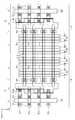
도 15 및 도 16은 본 발명의 제 1 실시예에 따른 반도체 메모리 장치의 메모리 블록들의 배치구조를 설명하기 위한 평면도들이다.15 and 16 are plan views for explaining an arrangement structure of memory blocks of the semiconductor memory device according to the first embodiment of the present invention.
실시예들에 따르면, 반도체 메모리 장치는 복수의 메모리 블록들(BLK)을 포함하며, 메모리 블록들(BLK)은 서로 인접하게 배치될 수 있다. 도 11 내지 도 14에 도시된 실시예와 실질적으로 동일한 구성 요소에 대해서는 동일한 도면 부호를 사용하며, 해당 구성 요소에 대한 상세한 설명은 생략하기로 한다.According to the embodiments, the semiconductor memory device includes a plurality of memory blocks BLK, and the memory blocks BLK may be disposed adjacent to each other. Elements that are substantially the same as those of the embodiment shown in Figs. 11 to 14 are denoted by the same reference numerals, and detailed description thereof will be omitted.
도 15를 참조하면, 인접하는 메모리 블록들(BLK)은 로컬 비트라인 구조체들(LBLS)이 인접하도록 배치될 수 있다. 즉, 인접하는 메모리 블록들(BLK)이 미러(mirror) 대칭으로 배치될 수 있다. 그리고, 서로 다른 메모리 블록들(BLK)의 로컬 비트라인들(LBL1~LBL4)은 전기적으로 분리될 수 있다. 즉, 제 1 방향에서 인접하는 로컬 비트라인 구조체들(LBLS)을 서로 이격되어 배치될 수 있다. 서로 다른 메모리 블록들(BLK) 내의 로컬 비트라인들이 전기적으로 분리될 수 있다.Referring to FIG. 15, adjacent memory blocks BLK may be arranged such that local bit line structures LBLS are adjacent to each other. That is, adjacent memory blocks BLK may be arranged mirror symmetrically. The local bit lines LBL1 to LBL4 of the different memory blocks BLK can be electrically separated. That is, adjacent local bit line structures LBLS in the first direction may be disposed apart from each other. The local bit lines in the different memory blocks BLK can be electrically separated.
복수의 메모리 블록들(BLK)은 수직 선택 라인들(VSL) 및 글로벌 비트라인들(GBL)을 공유할 수 있다. 수직 선택 라인들(VSL)은 각 메모리 블록들(BLK) 내의 선택 라인 콘택 플러그들(127)에 접속될 수 있다. 글로벌 비트라인들(GBL)은 각 메모리 블록들(BLK) 내의 제 2 전극 플러그들(137)에 접속될 수 있다.The plurality of memory blocks BLK may share the vertical selection lines VSL and the global bit lines GBL. Vertical select lines VSL may be connected to select line contact plugs 127 in each memory block BLK. The global bit lines GBL may be connected to the second electrode plugs 137 in the respective memory blocks BLK.
도 16을 참조하면, 인접하는 메모리 블록들(BLK)은 메모리 블록 선택부(도 3의 130 참조)를 공유할 수 있다. 다시 말해, 인접하는 셀 어레이 영역(10)들 사이에 하나의 블록 선택 영역(25)이 배치될 수 있다. 인접하는 메모리 블록들(BLK)은 블록 선택 트랜지스터들(BST)의 제 2 불순물 영역들 및 제 2 전극 플러그들(137)을 공유할 수 있다.Referring to FIG. 16, adjacent memory blocks BLK may share a memory block selector (see 130 in FIG. 3). In other words, one
보다 상세하게, 블록 선택 영역(25)의 기판(100)에 복수의 활성 영역들(131)이 정의될 수 있으며, 활성 영역들(131)을 가로지르는 두 개의 블록 선택 라인들(BSL)이 배치될 수 있다. 그리고, 블록 선택 라인들(BSL) 사이의 활성 영역들(131) 내에 제 2 불순물 영역들이 공통으로 형성될 수 있다.More specifically, a plurality of
도 17은 본 발명의 제 2 실시예에 따른 반도체 메모리 장치의 메모리 블록을 나타내는 사시도이다. 도 18은 도 17에 도시된 메모리 블록의 평면도이다.17 is a perspective view showing a memory block of the semiconductor memory device according to the second embodiment of the present invention. 18 is a plan view of the memory block shown in Fig.
도 17 및 도 18을 참조하면, 기판(100)은 셀 어레이 영역(10)과 주변 회로 영역(20)을 포함한다. 그리고, 주변 회로 영역(20)은 셀 어레이 영역(10)과 인접한 수직 셀 그룹 선택 영역(21), 콘택 영역(23), 및 이들 사이의 블록 선택 영역(25)을 포함한다.Referring to FIGS. 17 and 18, the
이 실시예에 따르면, 로컬 비트라인 구조체들(LBLS)은 셀 어레이 영역(10)에서 수직 셀 그룹 선택 영역(21) 및 블록 선택 영역(25)을 가로질러 콘택 영역(23)으로 연장될 수 있다. 도 13을 참조하여 설명한 것처럼, 기판(100)으로부터 동일한 수직적 높이에 위치하는 로컬 비트라인들(LBL1~LBL4)은, 콘택 영역(23)에서 연결 패드부(도 14의 ICP 참조)에 공통으로 연결될 수 있다.According to this embodiment, the local bit line structures LBLS can extend from the
수직 셀 그룹 선택 영역(21)의 기판(100) 상에, 도 12를 참조하여 설명한 것처럼, 복수의 수직 선택 게이트 전극들(VSG)이 배치될 수 있다. 하나의 로컬 비트라인 구조체(LBLS) 양측에 배치된 수직 선택 게이트 전극들(VSG)은 전기적으로 연결될 수 있다.On the
이 실시예에 따르면, 블록 선택 영역(25)의 기판(100) 상에 복수의 수직 블록 선택 게이트 전극들(VBSG)이 배치될 수 있다. 수직 블록 선택 게이트 전극들(VBSG)은 로컬 비트라인 구조체들(LBLS) 양측에 게이트 절연막을 개재하여 배치될 수 있다. 그리고 블록 선택 영역(25)에 배치된 복수의 수직 블록 선택 게이트 전극들(VBSG)은 블록 선택 라인(BSL)에 공통으로 연결될 수 있다. 블록 선택 라인(BSL)은 로컬 비트라인 구조체들(LBLS) 상에서 제 2 방향(D2)으로 연장될 수 있다.According to this embodiment, a plurality of vertical block select gate electrodes VBSG may be disposed on the
도 17 및 도 18에 도시된 실시예에 따르면, 메모리 블록 선택부(도 3의 130 참조)가 기판(100)에 대해 수직하는 수직 블록 게이트 전극들(VBSG)을 포함하므로, 반도체 메모리 장치의 집적도를 보다 향상시킬 수 있다.17 and 18, since the memory block selection portion 130 (see FIG. 3) includes the vertical block gate electrodes VBSG perpendicular to the
도 19는 본 발명의 제 3 실시예에 따른 반도체 메모리 장치의 메모리 블록을 나타내는 사시도이다. 도 20은 도 19에 도시된 메모리 블록의 평면도이다.19 is a perspective view showing a memory block of a semiconductor memory device according to a third embodiment of the present invention. 20 is a plan view of the memory block shown in Fig.
도 19 및 도 20을 참조하면, 기판(100)은 셀 어레이 영역(10) 및 주변 회로 영역(20)을 포함한다. 주변 회로 영역(20)의 기판(100) 상에 수직 셀 그룹 선택부들(도 3의 120 참조)과, 메모리 블록 선택부(도 2의 130 참조)가 배치될 수 있다. 여기서, 메모리 블록 선택부(도 3의 130 참조) 상에 수직 셀 그룹 선택부들(도 3의 120 참조)이 배치될 수 있다. 다시 말해, 수직적 높이에 있어서, 메모리 블록 선택부(도 3의 130 참조)는 수직 셀 그룹 선택부들(도 3의 120 참조)과 기판(100) 사이에 배치될 수 있다. 즉, 메모리 블록 선택부(도 3의 130 참조)와 수직 셀 그룹 선택부들(도 3의 120 참조)은 수직적으로 서로 다른 높이에 배치될 수 있다.19 and 20, a
보다 상세히 설명하면, 주변 회로 영역(20)의 기판(100)에 활성 영역들(131)을 정의하는 소자 분리막들(132)이 형성될 수 있다. 블록 선택 영역(25)의 기판(100) 상에, 게이트 절연막을 개재하여 활성 영역들(131)을 가로지르는 블록 선택 라인(BSL)이 배치될 수 있다. 블록 선택 라인(BSL)은 제 2 방향(D2)으로 연장될 수 있다. 블록 선택 라인(BSL) 일측의 활성 영역들 내에 제 1 불순물 영역들이 형성될 수 있으며, 블록 선택 라인(BSL) 타측의 활성 영역들(131) 내에 제 2 불순물 영역들이 형성될 수 있다. 제 1 불순물 영역들 각각에 제 1 전극 플러그(135)가 접속될 수 있으며, 제 2 불순물 영역들 각각에 제 2 전극 플러그(137)가 접속될 수 있다.More specifically, the
메모리 블록 선택부(130)가 형성된 기판(100) 상에 도 12에 도시된 구조와 동일한 메모리 셀 어레이(110) 및 수직 셀 그룹 선택부들(120)이 배치될 수 있다. 메모리 셀 어레이(110)의 로컬 비트라인 구조체들(LBLS)은 셀 어레이 영역(10)에서 주변 회로 영역(20)으로 연장되며, 동일한 수직적 높이에 배치된 로컬 비트라인들(LBL1~LBL4)은 연결 패드부(도 14의 ICP 참조)에 공통으로 연결된다. 연결 패드부(도 14의 ICP 참조) 각각에 비트라인 콘택 플러그(BPLG)가 접속된다. 수직 셀 그룹 선택부들(도 3 의 120 참조)의 수직 선택 게이트 전극들(VSG)은, 수직적 관점에서, 블록 선택 라인(BSL) 상에 배치될 수 있다.The
제 1 불순물 영역과 접속된 제 1 전극 플러그(135)는 기판(100)의 상면에 대해 수직적으로 연장되어 비트라인 도전 패드(BLCP)를 통해 비트라인 콘택 플러그(BPLG)와 연결된다. 이 실시예에 따르면, 제 1 불순물 영역들에 대응하는 제 1 전극 플러그들(135)은 평면적 관점에서 로컬 비트라인 구조체들(LBLS) 사이에 배치될 수 있다. 마찬가지로, 제 2 불순물 영역들에 대응하는 제 2 전극 플러그들(137)은 평면적 관점에서 로컬 비트라인 구조체들(LBLS) 사이에 배치될 수 있으며, 수직 선택 게이트 전극(VSG)과 제 1 및 제 2 수직 워드라인들(VWL1, VWL2) 사이에 배치될 수 있다. 제 2 전극 플러그들(137) 각각에 글로벌 비트라인(GBL)이 접속될 수 있다. 글로벌 비트라인들(GBL)은 서로 전기적으로 분리되며, 제 1 방향(D1)으로 나란히 연장될 수 있다.The
나아가, 이 실시예에 따르면, 도면에는 도시하지 않았으나, 블록 선택 라인 디코더(도 1의 1 참조), 워드라인 디코더(도 1의 2 참조), 수직 선택 라인 디코더(도 1의 3 참조) 비트라인 디코더(도 1의 4 참조), 및 제어 회로와 같은 로직 회로들이, 메모리 셀 어레이(110)와 기판(100) 사이에 배치될 수도 있다.1), a word line decoder (see 2 in FIG. 1), a vertical select line decoder (see 3 in FIG. 1), a bit line decoder A decoder (see 4 in FIG. 1), and logic circuits such as a control circuit, may be disposed between the
도 19 및 도 20에 도시된 실시예에 따르면, 메모리 블록 선택부(130)가 수직 셀 그룹 선택부들(120) 아래에 배치되므로, 반도체 메모리 장치의 집적도를 보다 향상시킬 수 있다.According to the embodiment shown in FIGS. 19 and 20, since the memory
상술된 실시예들에 따른 반도체 메모리 장치는 다양한 형태들의 반도체 패키지(semiconductor package)로 구현될 수 있다. 예를 들면, 본 발명의 실시예들에 따른 반도체 메모리 장치는 PoP(Package on Package), Ball grid arrays(BGAs), Chip scale packages(CSPs), Plastic Leaded Chip Carrier(PLCC), Plastic Dual In-Line Package(PDIP), Die in Waffle Pack, Die in Wafer Form, Chip On Board(COB), Ceramic Dual In-Line Package(CERDIP), Plastic Metric Quad Flat Pack(MQFP), Thin Quad Flatpack(TQFP), Small Outline(SOIC), Shrink Small Outline Package(SSOP), Thin Small Outline(TSOP), Thin Quad Flatpack(TQFP), System In Package(SIP), Multi Chip Package(MCP), Wafer-level Fabricated Package(WFP), Wafer-Level Processed Stack Package(WSP) 등의 방식으로 패키징될 수 있다. 본 발명의 실시예들에 따른 반도체 메모리 장치가 실장된 패키지는 반도체 메모리 장치를 제어하는 컨트롤러 및/또는 논리 소자 등을 더 포함할 수도 있다.The semiconductor memory device according to the above-described embodiments may be implemented in various types of semiconductor packages. For example, the semiconductor memory device according to embodiments of the present invention may be implemented as a package on package (PoP), ball grid arrays (BGAs), chip scale packages (CSPs), plastic leaded chip carriers Die in Wafer Form, Chip On Board (COB), Ceramic Dual In-Line Package (CERDIP), Plastic Metric Quad Flat Pack (MQFP), Thin Quad Flatpack (TQFP), Small Outline (SOIC), Shrink Small Outline Package (SSOP), Thin Small Outline (TSOP), Thin Quad Flatpack (TQFP), System In Package (SIP), Multi Chip Package (MCP), Wafer-level Fabricated Package -Level Processed Stack Package (WSP) or the like. The package on which the semiconductor memory device according to the embodiments of the present invention is mounted may further include a controller and / or a logic element for controlling the semiconductor memory device.
도 21은 본 발명의 실시예들에 따른 반도체 메모리 장치를 포함하는 전자 시스템의 블록도이다.21 is a block diagram of an electronic system including a semiconductor memory device in accordance with embodiments of the present invention.
도 21을 참조하면, 본 발명의 실시예에 따른 전자 시스템(1100)은 컨트롤러(1110), 입출력 장치(1120, I/O), 메모리 장치(1130, memory device), 인터페이스(1140) 및 버스(1150, bus)를 포함할 수 있다. 컨트롤러(1110), 입출력 장치(1120), 메모리 장치(1130) 및/또는 인터페이스(1140)는 버스(1150)를 통하여 서로 결합 될 수 있다. 버스(1150)는 데이터들이 이동되는 통로(path)에 해당한다.21, an
컨트롤러(1110)는 마이크로프로세서, 디지털 신호 프로세스, 마이크로 컨트롤러, 및 이들과 유사한 기능을 수행할 수 있는 논리 소자들 중에서 적어도 하나를 포함할 수 있다. 입출력 장치(1120)는 키패드(keypad), 키보드 및 디스플레이 장치 등을 포함할 수 있다. 메모리 장치(1130)는 데이터 및/또는 명령어 등을 저장할 수 있다. 메모리 장치(1130)는 도면들을 참조하여 설명된 본 발명의 실시예들의 반도체 메모리 장치들 중에서 적어도 하나를 포함할 수 있다. 또한, 메모리 장치(1130)는 다른 형태의 반도체 메모리 장치(ex, 디램 소자 및/또는 에스램 소자 등)를 더 포함할 수 있다. 인터페이스(1140)는 통신 네트워크로 데이터를 전송하거나 통신 네트워크로부터 데이터를 수신하는 기능을 수행할 수 있다. 인터페이스(1140)는 유선 또는 무선 형태일 수 있다. 예를 들어, 인터페이스(1140)는 안테나 또는 유무선 트랜시버 등을 포함할 수 있다. 도시하지 않았지만, 전자 시스템(1100)은 컨트롤러(1110)의 동작을 향상시키기 위한 동작 메모리로서, 고속의 디램 및/또는 에스램 등을 더 포함할 수도 있다.The
전자 시스템(1100)은 개인 휴대용 정보 단말기(PDA, personal digital assistant) 포터블 컴퓨터(portable computer), 웹 타블렛(web tablet), 무선 전화기(wireless phone), 모바일 폰(mobile phone), 디지털 뮤직 플레이어(digital music player), 메모리 카드(memory card), 또는 정보를 무선환경에서 송신 및/또는 수신할 수 있는 모든 전자 제품에 적용될 수 있다.
도 22는 본 발명의 실시예들에 따른 반도체 메모리 장치를 포함하는 메모리 카드를 나타내는 블록도이다.22 is a block diagram showing a memory card including a semiconductor memory device according to embodiments of the present invention.
도 22를 참조하면, 본 발명의 일 실시예에 따른 메모리 카드(1200)는 본 발명의 실시예들에 따른 반도체 메모리 장치를 포함할 수 있다. 또한, 메모리 장치(1210)는 다른 형태의 반도체 메모리 장치(ex, 디램 소자 및/또는 에스램 소자 등)를 더 포함할 수 있다. 메모리 카드(1200)는 호스트(Host)와 메모리 장치(1210) 간의 데이터 교환을 제어하는 메모리 컨트롤러(1220)를 포함할 수 있다.Referring to FIG. 22, a
메모리 컨트롤러(1220)는 메모리 카드의 전반적인 동작을 제어하는 프로세싱 유닛(1222)을 포함할 수 있다. 또한, 메모리 컨트롤러(1220)는 프로세싱 유닛(1222)의 동작 메모리로써 사용되는 에스램(1221, SRAM)을 포함할 수 있다. 이에 더하여, 메모리 컨트롤러(1220)는 호스트 인터페이스(1223), 메모리 인터페이스(1225)를 더 포함할 수 있다. 호스트 인터페이스(1223)는 메모리 카드(1200)와 호스트(Host)간의 데이터 교환 프로토콜을 구비할 수 있다. 메모리 인터페이스(1225)는 메모리 컨트롤러(1220)와 메모리 장치(1210)를 접속시킬 수 있다. 더 나아가서, 메모리 컨트롤러(1220)는 에러 정정 블록(1224, Ecc)를 더 포함할 수 있다. 에러 정정 블록(1224)은 메모리 장치(1210)로부터 독출된 데이터의 에러를 검출 및 정정할 수 있다. 도시하지 않았지만, 메모리 카드(1200)는 호스트(Host)와의 인터페이싱을 위한 코드 데이터를 저장하는 롬 장치(ROM device)를 더 포함할 수도 있다. 메모리 카드(1200)는 휴대용 데이터 저장 카드로 사용될 수 있다. 이와는 달리, 메모리 카드(1200)는 컴퓨터시스템의 하드디스크를 대체할 수 있는 고상 디스트(SSD, Solid State Disk)로도 구현될 수 있다.The
이상, 첨부된 도면을 참조하여 본 발명의 실시예를 설명하였지만, 본 발명이 속하는 기술분야에서 통상의 지식을 가진 자는 본 발명이 그 기술적 사상이나 필수적인 특징을 변경하지 않고서 다른 구체적인 형태로 실시될 수 있다는 것을 이해할 수 있을 것이다. 그러므로 이상에서 기술한 실시예에는 모든 면에서 예시적인 것이며 한정적이 아닌 것으로 이해해야만 한다.
While the present invention has been described in connection with what is presently considered to be practical exemplary embodiments, it is to be understood that the invention is not limited to the disclosed embodiments, but, on the contrary, It will be understood. It is therefore to be understood that the above-described embodiments are illustrative and not restrictive in every respect.
Claims (10)
Translated fromKorean상기 메모리 블록들에 공통으로 연결되는 글로벌 비트라인들;
상기 메모리 블록들 중 어느 하나와 상기 글로벌 비트라인들 간의 전기적 연결을 제어하는 블록 선택 라인들;
상기 적층 구조체들 중 어느 하나와 상기 글로벌 비트라인들 간의 연결을 제어하는 수직 선택 라인들;
상기 로컬 비트라인들을 가로지르며, 서로 다른 상기 적층 구조체들의 상기 제 1 수직 워드라인들을 연결하는 제 1 수평 워드라인; 및
상기 로컬 비트라인들을 가로지르며, 서로 다른 상기 적층 구조체들의 상기 제 2 수직 워드라인들을 연결하는 제 2 수평 워드라인을 포함하는 반도체 메모리 장치.A plurality of memory blocks, each of the memory blocks including a plurality of stacked structures including a plurality of local bit lines stacked on a substrate, first vertical word lines crossing between the first sidewalls of the stacked structures, Second vertical word lines crossing between the second sidewalls of the stacked structures opposite to the first sidewalls, first variable resistive elements interposed between the stacked structures and the first vertical word lines, And second variable resistance elements interposed between the stacked structures and the second vertical word lines;
Global bit lines commonly connected to the memory blocks;
Block select lines for controlling an electrical connection between any one of the memory blocks and the global bit lines;
Vertical selection lines for controlling connection between any one of the stacked structures and the global bit lines;
A first horizontal word line crossing the local bit lines and connecting the first vertical word lines of the different stacked structures; And
And a second horizontal word line crossing the local bit lines and connecting the second vertical word lines of the different stacked structures.
상기 수직 선택 라인들은 서로 전기적으로 분리되며, 상기 적층 구조체들의 측벽들을 가로지르는 반도체 메모리 장치.The method according to claim 1,
Wherein the vertical select lines are electrically separated from each other and cross the sidewalls of the stacked structures.
상기 기판은 셀 어레이 영역 및 주변 회로 영역을 포함하고,
상기 로컬 비트라인들 각각은 상기 셀 어레이 영역에 배치되는 복수의 배선부들, 상기 주변 회로 영역에 배치되어 상기 배선부들을 수평적으로 연결하는 연결 패드부, 및 상기 연결 패드부로부터 수평적으로 돌출된 콘택 패드부를 포함하되,
상기 적층 구조체들의 상기 콘택 패드부들은 상기 셀 어레이 영역으로부터 실질적으로 동일한 수평적 거리에 배치되는 반도체 메모리 장치.The method according to claim 1,
Wherein the substrate includes a cell array region and a peripheral circuit region,
Wherein each of the local bit lines includes a plurality of wiring portions arranged in the cell array region, a connection pad portion disposed in the peripheral circuit region and horizontally connecting the wiring portions, And a contact pad portion,
Wherein the contact pad portions of the stacked structures are disposed at substantially the same horizontal distance from the cell array region.
상기 적층 구조체들의 상기 콘택 패드부들은, 평면적 관점에서, 상기 배선부들의 장축 방향에 실질적으로 수직한 방향으로 배열되고,
상기 적층 구조체들의 상기 콘택 패드부들 각각에 접속되는 콘택 플러그들을 더 포함하되, 상기 콘택 플러그들은 상기 셀 어레이 영역으로부터 실질적으로 동일한 수평적 거리에 배치되는 반도체 메모리 장치.5. The method of claim 4,
The contact pad portions of the stacked structures are arranged in a direction substantially perpendicular to the major axis direction of the wiring portions from a plan view point,
Further comprising contact plugs connected to each of the contact pad portions of the stacked structures, wherein the contact plugs are disposed at substantially the same horizontal distance from the cell array region.
상기 셀 어레이 영역의 상기 기판 상에 배치된 복수의 수직 셀 그룹들로서, 상기 수직 셀 그룹들 각각은 상기 기판 상에 적층된 복수의 로컬 비트라인들, 상기 로컬 비트라인들의 제 1 측벽들의 사이를 가로지르는 제 1 수직 워드라인들, 상기 제 1 측벽들과 대향하는 상기 로컬 비트라인들의 제 2 측벽들의 사이를 가로지르는 제 2 수직 워드라인들, 상기 로컬 비트라인들과 상기 제 1 수직 워드라인들 사이에 개재된 제 1 메모리 요소들, 및 상기 로컬 비트라인들과 상기 제 2 수직 워드라인들 사이에 개재된 제 2 메모리 요소들을 포함하는 것;
상기 주변 회로 영역의 상기 기판 상에 배치되며, 상기 수직 셀 그룹들 각각에 연결된 수직 셀 그룹 선택부들; 및
상기 주변 회로 영역의 상기 기판 상에 배치되며, 상기 수직 셀 그룹 선택부들에 공통으로 연결되는 메모리 블록 선택부를 포함하되,
상기 제 1 수직 워드라인들은, 평면적 관점에서, 상기 제 2 수직 워드라인들의 사선방향에 배치되는 반도체 메모리 장치.A substrate including a cell array region and a peripheral circuit region;
A plurality of vertical cell groups disposed on the substrate of the cell array region, each of the vertical cell groups comprising a plurality of local bit lines stacked on the substrate, Second vertical word lines crossing between second sidewalls of the local bit lines opposite to the first sidewalls, first vertical word lines extending between the local bit lines and the first vertical word lines, And second memory elements interposed between the local bit lines and the second vertical word lines;
Vertical cell group selectors arranged on the substrate of the peripheral circuit region and connected to each of the vertical cell groups; And
And a memory block selector disposed on the substrate of the peripheral circuit area and connected in common to the vertical cell group selectors,
Wherein the first vertical word lines are arranged in a diagonal direction of the second vertical word lines in a plan view.
상기 제 1 및 제 2 수직 워드라인들은 수평적으로 인접하는 상기 로컬 비트라인들 간의 거리의 1/2보다 큰 폭을 갖는 반도체 메모리 장치.The method according to claim 6,
Wherein the first and second vertical word lines have a width greater than 1/2 of a distance between the horizontally adjacent local bit lines.
상기 로컬 비트라인들을 가로지르며, 서로 다른 상기 수직 셀 그룹들의 상기 제 1 수직 워드라인들을 연결하는 제 1 수평 워드라인; 및
상기 로컬 비트라인들을 가로지르면, 서로 다른 상기 수직 셀 그룹들의 상기 제 2 수직 워드라인들을 연결하는 제 2 수평 워드라인을 더 포함하는 반도체 메모리 장치.The method according to claim 6,
A first horizontal word line crossing the local bit lines and connecting the first vertical word lines of the different vertical cell groups; And
And a second horizontal word line connecting the second vertical word lines of the different vertical cell groups when crossing the local bit lines.
상기 제 1 및 제 2 수평 워드라인들은 상기 기판으로부터 서로 다른 수직적 거리에 배치되는 반도체 메모리 장치.10. The method of claim 9,
Wherein the first and second horizontal word lines are disposed at different vertical distances from the substrate.
Priority Applications (2)
| Application Number | Priority Date | Filing Date | Title |
|---|---|---|---|
| KR1020120107192AKR101965614B1 (en) | 2012-09-26 | 2012-09-26 | Semiconductor memory device |
| US14/037,547US9183893B2 (en) | 2012-09-26 | 2013-09-26 | Semiconductor memory device |
Applications Claiming Priority (1)
| Application Number | Priority Date | Filing Date | Title |
|---|---|---|---|
| KR1020120107192AKR101965614B1 (en) | 2012-09-26 | 2012-09-26 | Semiconductor memory device |
Publications (2)
| Publication Number | Publication Date |
|---|---|
| KR20140043262A KR20140043262A (en) | 2014-04-09 |
| KR101965614B1true KR101965614B1 (en) | 2019-04-04 |
Family
ID=50338698
Family Applications (1)
| Application Number | Title | Priority Date | Filing Date |
|---|---|---|---|
| KR1020120107192AActiveKR101965614B1 (en) | 2012-09-26 | 2012-09-26 | Semiconductor memory device |
Country Status (2)
| Country | Link |
|---|---|
| US (1) | US9183893B2 (en) |
| KR (1) | KR101965614B1 (en) |
Families Citing this family (22)
| Publication number | Priority date | Publication date | Assignee | Title |
|---|---|---|---|---|
| JP2015176910A (en)* | 2014-03-13 | 2015-10-05 | 株式会社東芝 | semiconductor memory |
| US9455257B2 (en)* | 2014-09-04 | 2016-09-27 | Kabushiki Kaisha Toshiba | Semiconductor memory device and method of manufacturing the same |
| US9349446B2 (en)* | 2014-09-04 | 2016-05-24 | Kabushiki Kaisha Toshiba | Semiconductor memory device and method of controlling the same |
| KR102157359B1 (en)* | 2014-12-16 | 2020-09-17 | 삼성전자 주식회사 | Resistive Memory Device including column decoder and Operating Method thereof |
| KR102275540B1 (en) | 2014-12-18 | 2021-07-13 | 삼성전자주식회사 | Variable Resistance memory device |
| KR20160128731A (en)* | 2015-04-29 | 2016-11-08 | 에스케이하이닉스 주식회사 | Three dimension semiconductor device |
| JP2016225614A (en)* | 2015-05-26 | 2016-12-28 | 株式会社半導体エネルギー研究所 | Semiconductor device |
| US9502103B1 (en)* | 2015-10-06 | 2016-11-22 | Kabushiki Kaisha Toshiba | Semiconductor memory device |
| WO2018180228A1 (en)* | 2017-03-31 | 2018-10-04 | ソニーセミコンダクタソリューションズ株式会社 | Memory device |
| KR102366798B1 (en)* | 2017-06-13 | 2022-02-25 | 삼성전자주식회사 | Semiconductor devices |
| US10490602B2 (en)* | 2017-09-21 | 2019-11-26 | Micron Technology, Inc. | Three dimensional memory arrays |
| US10083734B1 (en) | 2017-11-06 | 2018-09-25 | Micron Technology, Inc. | Memory arrays |
| KR102667899B1 (en)* | 2018-10-02 | 2024-05-23 | 삼성전자주식회사 | Three dimensional semiconductor memory device |
| KR102682131B1 (en) | 2018-11-15 | 2024-07-08 | 삼성전자주식회사 | Nonvolatile memory device and operating method of the same |
| KR102707465B1 (en) | 2018-12-14 | 2024-09-23 | 삼성전자주식회사 | Three-dimensional semiconductor devices |
| KR102710732B1 (en) | 2019-07-30 | 2024-09-27 | 삼성전자주식회사 | Nonvolatile memory device and operating method of the same |
| KR102762975B1 (en) | 2019-09-06 | 2025-02-10 | 삼성전자주식회사 | Semiconductor device including data storage structrue |
| JP2021153080A (en)* | 2020-03-24 | 2021-09-30 | キオクシア株式会社 | Semiconductor storage device |
| KR102831348B1 (en) | 2020-11-19 | 2025-07-07 | 삼성전자주식회사 | Semiconductor memory device |
| US11849655B2 (en) | 2021-04-14 | 2023-12-19 | Taiwan Semiconductor Manufacturing Co., Ltd. | Semiconductor memory devices with electrically isolated stacked bit lines and methods of manufacture |
| CN113903374B (en)* | 2021-09-30 | 2024-11-12 | 武汉新芯集成电路股份有限公司 | Storage device and method for manufacturing the same |
| US20240074142A1 (en)* | 2022-08-29 | 2024-02-29 | Micron Technology, Inc. | Microelectronic devices, related memory devices, electronic systems, and methods |
Family Cites Families (15)
| Publication number | Priority date | Publication date | Assignee | Title |
|---|---|---|---|---|
| JP2009266946A (en) | 2008-04-23 | 2009-11-12 | Toshiba Corp | Three-dimensional stacked nonvolatile semiconductor memory |
| JP5193796B2 (en) | 2008-10-21 | 2013-05-08 | 株式会社東芝 | Three-dimensional stacked nonvolatile semiconductor memory |
| KR20100069391A (en)* | 2008-12-16 | 2010-06-24 | 삼성전자주식회사 | 3d memory architecture of nand-type flash for intersecting gate and multi-layer perpendicularly |
| TWI433302B (en) | 2009-03-03 | 2014-04-01 | Macronix Int Co Ltd | Self-aligned three-dimensional spatial memory array of integrated circuit and manufacturing method thereof |
| US7983065B2 (en) | 2009-04-08 | 2011-07-19 | Sandisk 3D Llc | Three-dimensional array of re-programmable non-volatile memory elements having vertical bit lines |
| KR101036155B1 (en) | 2009-07-09 | 2011-05-23 | 서울대학교산학협력단 | NAND flash memory array with star structure and manufacturing method thereof |
| KR101028994B1 (en) | 2009-09-07 | 2011-04-12 | 주식회사 하이닉스반도체 | Non-volatile memory device having a three-dimensional structure and method of manufacturing the same |
| KR20110040461A (en)* | 2009-10-14 | 2011-04-20 | 삼성전자주식회사 | Nonvolatile Memory Device and Manufacturing Method Thereof |
| KR20110095646A (en) | 2010-02-19 | 2011-08-25 | 충남대학교산학협력단 | Method for preparing saccharide material from algae using solution plasma treatment and method for producing biofuel using the same |
| KR101702060B1 (en)* | 2010-02-19 | 2017-02-02 | 삼성전자주식회사 | Interconnection structure for three-dimensional semiconductor device |
| US20110241077A1 (en) | 2010-04-06 | 2011-10-06 | Macronix International Co., Ltd. | Integrated circuit 3d memory array and manufacturing method |
| US8547720B2 (en)* | 2010-06-08 | 2013-10-01 | Sandisk 3D Llc | Non-volatile memory having 3D array of read/write elements with efficient decoding of vertical bit lines and word lines |
| KR101162197B1 (en) | 2010-06-15 | 2012-07-05 | 서울대학교산학협력단 | 3d stacked nand flash memory array having connection gate and fabrication method of the same |
| US9030859B2 (en)* | 2010-12-14 | 2015-05-12 | Sandisk 3D Llc | Three dimensional non-volatile storage with dual layers of select devices |
| US8824183B2 (en)* | 2010-12-14 | 2014-09-02 | Sandisk 3D Llc | Non-volatile memory having 3D array of read/write elements with vertical bit lines and select devices and methods thereof |
- 2012
- 2012-09-26KRKR1020120107192Apatent/KR101965614B1/enactiveActive
- 2013
- 2013-09-26USUS14/037,547patent/US9183893B2/enactiveActive
Also Published As
| Publication number | Publication date |
|---|---|
| US9183893B2 (en) | 2015-11-10 |
| KR20140043262A (en) | 2014-04-09 |
| US20140085961A1 (en) | 2014-03-27 |
Similar Documents
| Publication | Publication Date | Title |
|---|---|---|
| KR101965614B1 (en) | Semiconductor memory device | |
| US8824184B2 (en) | Semiconductor memory devices | |
| KR101952272B1 (en) | Semiconductor memory devices | |
| KR101567024B1 (en) | Semiconductor device | |
| US8338224B2 (en) | Resistance-type random access memory device having three-dimensional bit line and word line patterning | |
| US9679947B2 (en) | Semiconductor memory device | |
| KR102031187B1 (en) | Vertical type memory device | |
| KR102002802B1 (en) | Semiconductor device | |
| US9337239B2 (en) | Electronic device having flash memory array formed in at different level than variable resistance memory cells | |
| KR20100111165A (en) | Three dimensional memory device | |
| EP2819169A2 (en) | Semiconductor device | |
| KR20100033303A (en) | Non-volatile memory device and method of fabricating the same | |
| US11189630B2 (en) | Memory device and electronic device including insulating patterns with different thermal conductivities | |
| CN103715176B (en) | Semiconductor device | |
| KR20090109804A (en) | Nonvolatile Memory Device and Manufacturing Method Thereof | |
| CN112599159A (en) | Storage device | |
| US11616098B2 (en) | Three-dimensional memory arrays, and methods of forming the same | |
| TWI541827B (en) | High-density semiconductor memory device | |
| US20230284464A1 (en) | Three dimensional stacked semiconductor memory | |
| KR20130091153A (en) | Semiconductor memory device and fabricating the same | |
| KR102666992B1 (en) | Memory device | |
| US20130221487A1 (en) | Method of forming resistor of semiconductor memory device and structure thereof | |
| JP2023091744A (en) | semiconductor equipment |
Legal Events
| Date | Code | Title | Description |
|---|---|---|---|
| PA0109 | Patent application | Patent event code:PA01091R01D Comment text:Patent Application Patent event date:20120926 | |
| PG1501 | Laying open of application | ||
| A201 | Request for examination | ||
| PA0201 | Request for examination | Patent event code:PA02012R01D Patent event date:20170919 Comment text:Request for Examination of Application Patent event code:PA02011R01I Patent event date:20120926 Comment text:Patent Application | |
| E902 | Notification of reason for refusal | ||
| PE0902 | Notice of grounds for rejection | Comment text:Notification of reason for refusal Patent event date:20180814 Patent event code:PE09021S01D | |
| E701 | Decision to grant or registration of patent right | ||
| PE0701 | Decision of registration | Patent event code:PE07011S01D Comment text:Decision to Grant Registration Patent event date:20190218 | |
| PR0701 | Registration of establishment | Comment text:Registration of Establishment Patent event date:20190329 Patent event code:PR07011E01D | |
| PR1002 | Payment of registration fee | Payment date:20190401 End annual number:3 Start annual number:1 | |
| PG1601 | Publication of registration | ||
| PR1001 | Payment of annual fee | Payment date:20220223 Start annual number:4 End annual number:4 | |
| PR1001 | Payment of annual fee | Payment date:20230222 Start annual number:5 End annual number:5 | |
| PR1001 | Payment of annual fee | Payment date:20240227 Start annual number:6 End annual number:6 | |
| PR1001 | Payment of annual fee | Payment date:20250225 Start annual number:7 End annual number:7 |