KR101965256B1 - Organic light emitting display device and the manufacturing method thereof - Google Patents
Organic light emitting display device and the manufacturing method thereofDownload PDFInfo
- Publication number
- KR101965256B1 KR101965256B1KR1020120115610AKR20120115610AKR101965256B1KR 101965256 B1KR101965256 B1KR 101965256B1KR 1020120115610 AKR1020120115610 AKR 1020120115610AKR 20120115610 AKR20120115610 AKR 20120115610AKR 101965256 B1KR101965256 B1KR 101965256B1
- Authority
- KR
- South Korea
- Prior art keywords
- conductive layer
- layer
- conductive
- electrode
- light emitting
- Prior art date
- Legal status (The legal status is an assumption and is not a legal conclusion. Google has not performed a legal analysis and makes no representation as to the accuracy of the status listed.)
- Active
Links
- 238000004519manufacturing processMethods0.000titledescription2
- 239000010410layerSubstances0.000claimsdescription277
- 238000000034methodMethods0.000claimsdescription24
- 239000000758substrateSubstances0.000claimsdescription23
- 239000000463materialSubstances0.000claimsdescription13
- 239000012044organic layerSubstances0.000claims1
- 239000010408filmSubstances0.000description18
- 239000011229interlayerSubstances0.000description14
- 239000010409thin filmSubstances0.000description11
- 239000011368organic materialSubstances0.000description9
- 239000004020conductorSubstances0.000description7
- 230000003071parasitic effectEffects0.000description7
- 239000003990capacitorSubstances0.000description6
- 238000002425crystallisationMethods0.000description6
- PQXKHYXIUOZZFA-UHFFFAOYSA-Mlithium fluorideInorganic materials[Li+].[F-]PQXKHYXIUOZZFA-UHFFFAOYSA-M0.000description6
- VYPSYNLAJGMNEJ-UHFFFAOYSA-NSilicium dioxideChemical compoundO=[Si]=OVYPSYNLAJGMNEJ-UHFFFAOYSA-N0.000description5
- 230000008025crystallizationEffects0.000description5
- 229910052782aluminiumInorganic materials0.000description4
- 238000000151depositionMethods0.000description4
- 229910052751metalInorganic materials0.000description4
- 239000002184metalSubstances0.000description4
- 239000012535impuritySubstances0.000description3
- 229910021420polycrystalline siliconInorganic materials0.000description3
- 229920000642polymerPolymers0.000description3
- 229910004205SiNXInorganic materials0.000description2
- 229910004298SiO 2Inorganic materials0.000description2
- 229910021417amorphous siliconInorganic materials0.000description2
- 229910052681coesiteInorganic materials0.000description2
- 150000001875compoundsChemical class0.000description2
- 229910052906cristobaliteInorganic materials0.000description2
- 238000010586diagramMethods0.000description2
- 238000005530etchingMethods0.000description2
- 239000011521glassSubstances0.000description2
- 238000002347injectionMethods0.000description2
- 239000007924injectionSubstances0.000description2
- 229910010272inorganic materialInorganic materials0.000description2
- 239000011147inorganic materialSubstances0.000description2
- 229910052749magnesiumInorganic materials0.000description2
- 239000011159matrix materialSubstances0.000description2
- 238000000059patterningMethods0.000description2
- 239000002861polymer materialSubstances0.000description2
- 229920005591polysiliconPolymers0.000description2
- 230000008569processEffects0.000description2
- 238000004151rapid thermal annealingMethods0.000description2
- 230000009467reductionEffects0.000description2
- 239000000377silicon dioxideSubstances0.000description2
- 235000012239silicon dioxideNutrition0.000description2
- 229910052814silicon oxideInorganic materials0.000description2
- 229910052682stishoviteInorganic materials0.000description2
- 229910052905tridymiteInorganic materials0.000description2
- AIRCTMFFNKZQPN-UHFFFAOYSA-NAlOInorganic materials[Al]=OAIRCTMFFNKZQPN-UHFFFAOYSA-N0.000description1
- 229910017109AlONInorganic materials0.000description1
- YXTDPLJBZYYNNC-UHFFFAOYSA-NN-[4-[2-naphthalen-1-yl-4-(N-naphthalen-1-ylanilino)phenyl]phenyl]-N-phenylnaphthalen-1-amineChemical compoundC1(=CC=CC2=CC=CC=C12)C1=C(C=CC(=C1)N(C1=CC=CC2=CC=CC=C12)C1=CC=CC=C1)C1=CC=C(C=C1)N(C1=CC=CC=C1)C1=CC=CC2=CC=CC=C12YXTDPLJBZYYNNC-UHFFFAOYSA-N0.000description1
- 229920001609Poly(3,4-ethylenedioxythiophene)Polymers0.000description1
- 239000004642PolyimideSubstances0.000description1
- NIXOWILDQLNWCW-UHFFFAOYSA-Nacrylic acid groupChemical groupC(C=C)(=O)ONIXOWILDQLNWCW-UHFFFAOYSA-N0.000description1
- 230000004913activationEffects0.000description1
- QVGXLLKOCUKJST-UHFFFAOYSA-Natomic oxygenChemical compound[O]QVGXLLKOCUKJST-UHFFFAOYSA-N0.000description1
- 230000005540biological transmissionEffects0.000description1
- 239000002131composite materialSubstances0.000description1
- XCJYREBRNVKWGJ-UHFFFAOYSA-Ncopper(II) phthalocyanineChemical compound[Cu+2].C12=CC=CC=C2C(N=C2[N-]C(C3=CC=CC=C32)=N2)=NC1=NC([C]1C=CC=CC1=1)=NC=1N=C1[C]3C=CC=CC3=C2[N-]1XCJYREBRNVKWGJ-UHFFFAOYSA-N0.000description1
- 238000009792diffusion processMethods0.000description1
- 229920002457flexible plasticPolymers0.000description1
- 230000005484gravityEffects0.000description1
- 238000010438heat treatmentMethods0.000description1
- RBTKNAXYKSUFRK-UHFFFAOYSA-Nheliogen blueChemical compound[Cu].[N-]1C2=C(C=CC=C3)C3=C1N=C([N-]1)C3=CC=CC=C3C1=NC([N-]1)=C(C=CC=C3)C3=C1N=C([N-]1)C3=CC=CC=C3C1=N2RBTKNAXYKSUFRK-UHFFFAOYSA-N0.000description1
- 230000005525hole transportEffects0.000description1
- 238000007641inkjet printingMethods0.000description1
- 239000011810insulating materialSubstances0.000description1
- 150000002500ionsChemical class0.000description1
- 230000001678irradiating effectEffects0.000description1
- 238000005224laser annealingMethods0.000description1
- 238000012986modificationMethods0.000description1
- 230000004048modificationEffects0.000description1
- 229910052760oxygenInorganic materials0.000description1
- 239000001301oxygenSubstances0.000description1
- 229920003023plasticPolymers0.000description1
- 239000002985plastic filmSubstances0.000description1
- 229920002098polyfluorenePolymers0.000description1
- 229920001721polyimidePolymers0.000description1
- 238000007650screen-printingMethods0.000description1
- 238000007789sealingMethods0.000description1
- 239000002356single layerSubstances0.000description1
- 239000007790solid phaseSubstances0.000description1
- 238000007711solidificationMethods0.000description1
- 230000008023solidificationEffects0.000description1
- 239000000126substanceSubstances0.000description1
- TVIVIEFSHFOWTE-UHFFFAOYSA-Ktri(quinolin-8-yloxy)alumaneChemical compound[Al+3].C1=CN=C2C([O-])=CC=CC2=C1.C1=CN=C2C([O-])=CC=CC2=C1.C1=CN=C2C([O-])=CC=CC2=C1TVIVIEFSHFOWTE-UHFFFAOYSA-K0.000description1
- 238000001771vacuum depositionMethods0.000description1
Images


Classifications
- H—ELECTRICITY
- H10—SEMICONDUCTOR DEVICES; ELECTRIC SOLID-STATE DEVICES NOT OTHERWISE PROVIDED FOR
- H10K—ORGANIC ELECTRIC SOLID-STATE DEVICES
- H10K59/00—Integrated devices, or assemblies of multiple devices, comprising at least one organic light-emitting element covered by group H10K50/00
- H10K59/10—OLED displays
- H10K59/12—Active-matrix OLED [AMOLED] displays
- H10K59/131—Interconnections, e.g. wiring lines or terminals
- H10K59/1315—Interconnections, e.g. wiring lines or terminals comprising structures specially adapted for lowering the resistance
- H—ELECTRICITY
- H10—SEMICONDUCTOR DEVICES; ELECTRIC SOLID-STATE DEVICES NOT OTHERWISE PROVIDED FOR
- H10K—ORGANIC ELECTRIC SOLID-STATE DEVICES
- H10K50/00—Organic light-emitting devices
- H10K50/80—Constructional details
- H10K50/805—Electrodes
- H—ELECTRICITY
- H10—SEMICONDUCTOR DEVICES; ELECTRIC SOLID-STATE DEVICES NOT OTHERWISE PROVIDED FOR
- H10K—ORGANIC ELECTRIC SOLID-STATE DEVICES
- H10K59/00—Integrated devices, or assemblies of multiple devices, comprising at least one organic light-emitting element covered by group H10K50/00
- H10K59/10—OLED displays
- H10K59/12—Active-matrix OLED [AMOLED] displays
- H10K59/131—Interconnections, e.g. wiring lines or terminals
- H—ELECTRICITY
- H10—SEMICONDUCTOR DEVICES; ELECTRIC SOLID-STATE DEVICES NOT OTHERWISE PROVIDED FOR
- H10K—ORGANIC ELECTRIC SOLID-STATE DEVICES
- H10K59/00—Integrated devices, or assemblies of multiple devices, comprising at least one organic light-emitting element covered by group H10K50/00
- H10K59/80—Constructional details
- H10K59/805—Electrodes
Landscapes
- Engineering & Computer Science (AREA)
- Microelectronics & Electronic Packaging (AREA)
- Physics & Mathematics (AREA)
- Optics & Photonics (AREA)
- Electroluminescent Light Sources (AREA)
- Devices For Indicating Variable Information By Combining Individual Elements (AREA)
Abstract
Translated fromKoreanDescription
Translated fromKorean본 발명은 유기 발광 표시 장치 및 그 제조방법에 관한 것으로, 스캔 로드를 줄일 수 있는 유기 발광 표시 장치에 관한 것이다.BACKGROUND OF THE
일반적으로 유기 발광 표시 장치는 박막트랜지스터(Thin Film Transistor:TFT)와, 그 박막트랜지스터에 의해 구동되며 화상을 구현하는 유기 전계 발광 소자(이하 EL소자) 등을 구비하고 있다.2. Description of the Related Art Generally, an organic light emitting display device includes a thin film transistor (TFT) and an organic electroluminescent device (hereinafter referred to as an EL element) that is driven by the thin film transistor and realizes an image.
여기서, 상기 박막트랜지스터는 게이트전극과 활성층 및 소스드레인전극 등이 기판 상에 적층된 구조로 이루어진다. 따라서, 기판에 마련된 배선을 통해 게이트전극에 전류가 공급되면, 상기 활성층을 경유하여 소스드레인전극에 전류가 흐르게 되고, 동시에 이 소스드레인전극과 연결된 EL소자의 화소전극에 전류가 흐르게 된다.Here, the thin film transistor has a structure in which a gate electrode, an active layer, a source / drain electrode, and the like are stacked on a substrate. Accordingly, when a current is supplied to the gate electrode through the wiring provided in the substrate, a current flows to the source / drain electrode via the active layer, and at the same time, a current flows to the pixel electrode of the EL element connected to the source / drain electrode.
그리고, 상기 EL소자는 상기 화소전극 및 그와 대면하는 대향전극, 그리고 두 전극 사이에 개재된 발광층을 구비한다. 이와 같은 구조에서 상기한 대로 박막트랜지스터를 통해 화소전극에 전류가 흐르게 되면, 상기 화소전극과 대향전극 사이에 적정 전압이 형성되고, 이에 따라 상기 발광층에서 발광 동작이 일어나면서 화상이 구현된다.The EL element includes the pixel electrode, an opposing electrode facing the pixel electrode, and a light emitting layer interposed between the two electrodes. When a current flows to the pixel electrode through the thin film transistor as described above, an appropriate voltage is formed between the pixel electrode and the counter electrode, thereby realizing an image while the light emitting operation is performed in the light emitting layer.
한편, 유기 발광 표시 장치의 대형화로 인해서 게이트 배선 및 데이터 배선과 같은 배선의 저항이 증가되고 기생 커패시턴스의 증가로 인해 신호 지연이 발생하는 문제점이 있다.On the other hand, there is a problem that the resistance of the wiring such as the gate wiring and the data wiring is increased due to the enlargement of the organic light emitting display device, and the signal delay is caused due to the increase of the parasitic capacitance.
본 발명의 실시예는 배선의 저항을 감소시킬 수 있는 유기 발광 표시 장치를 제공한다.An embodiment of the present invention provides an organic light emitting display device capable of reducing a resistance of a wiring.
그리고, 본 발명의 실시예는 기생 커패시턴스를 감소시킬 수 있는 유기 발광 표시 장치를 제공한다.In addition, embodiments of the present invention provide an organic light emitting display device capable of reducing parasitic capacitance.
본 발명의 실시예에 따른 유기 발광 표시 장치는 제1 방향으로 연장된 복수 개의 제1 배선들; 상기 제1 방향과 교차하는 제2 방향으로 연장된 복수 개의 제2 배선들을 포함하고, 상기 제1 배선들 중 적어도 하나는 제1 도전층 및 상기 제1 도전층의 위에서부터 상기 제1 도전층과 동일한 층 또는 그 아래층상으로 연장된 제2 도전층;을 포함한다.An organic light emitting display according to an embodiment of the present invention includes a plurality of first wirings extending in a first direction; And a plurality of second wirings extending in a second direction intersecting with the first direction, at least one of the first wirings including a first conductive layer and a second conductive layer extending from the top of the first conductive layer to the first conductive layer, And a second conductive layer extending on the same layer or a layer thereunder.
그리고, 상기 제1 배선들과 상기 제2 배선들은 교차하여 복수 개의 화소들을 정의하며, 상기 복수 개의 화소들 각각은 화소 전극, 유기 발광층을 구비하는 중간층 및 대향 전극을 구비하는 유기발광소자과 게이트전극, 소스 및 드레인전극을 구비하는 스위칭소자를 포함하고, 상기 제2 도전층은 제1 도전층의 위에서부터 상기 대향 전극에 대해 멀어지는 방향으로 연장될 수 있다.The first wirings and the second wirings intersect each other to define a plurality of pixels. Each of the plurality of pixels includes an organic light emitting element and a gate electrode each having a pixel electrode, an intermediate layer having an organic light emitting layer, and a counter electrode, And a switching element having a source and a drain electrode, wherein the second conductive layer can extend in a direction away from the counter electrode from above the first conductive layer.
또한, 상기 제2 도전층은 상기 제1 도전층에 대해 멀어질수록 상기 대향 전극에 대해서도 멀어지게 연장될 수 있다.In addition, the second conductive layer can be extended away from the counter electrode as the distance from the first conductive layer increases.
그리고, 상기 제1 배선들은 상기 화소들에 주사 신호를 공급하는 스캔 배선들일 수 있다.The first wirings may be scan wirings for supplying scan signals to the pixels.
또한, 기판; 및 상기 기판상에 배치된 버퍼층;을 더 포함하고, 상기 버퍼층 위에 상기 제1 배선들 및 상기 제2 배선들이 형성될 수 있다.A substrate; And a buffer layer disposed on the substrate, wherein the first wires and the second wires are formed on the buffer layer.
그리고, 상기 제2 도전층의 일부는 상기 버퍼층상에 형성될 수 있다.A part of the second conductive layer may be formed on the buffer layer.
또한, 상기 버퍼층과 상기 제1 도전층 사이에 형성된 제1 절연층;을 더 포함할 수 있다.The first conductive layer may further include a first insulating layer formed between the buffer layer and the first conductive layer.
그리고, 상기 제1 절연층은 상기 제2 도전층의 일부가 상기 버퍼층과 접하도록 제1 개구가 형성될 수 있다.A first opening may be formed in the first insulating layer such that a portion of the second conductive layer contacts the buffer layer.
또한, 상기 제1 절연층 상에 배치되며, 상기 제1 도전층을 덮는 제2 절연층;을 더 포함할 수 있다.The first insulating layer may further include a second insulating layer disposed on the first insulating layer and covering the first conductive layer.
그리고, 상기 제2 절연층은 상기 제2 도전층의 일부가 상기 버퍼층 또는 상기 제1 절연층과 접하도록 제2 개구가 형성될 수 있다.A second opening may be formed in the second insulating layer such that a portion of the second conductive layer contacts the buffer layer or the first insulating layer.
또한, 상기 제1 도전층과 상기 제2 도전층은 상기 제2 절연층에 형성된 컨택홀을 통해 연결될 수 있다.The first conductive layer and the second conductive layer may be connected to each other through a contact hole formed in the second insulating layer.
그리고, 상기 제2 도전층은 상기 제1 도전층의 일부를 덮으면서 상기 버퍼층상에 배치될 수 있다.The second conductive layer may be disposed on the buffer layer while covering a portion of the first conductive layer.
또한, 상기 제1 도전층은 상기 게이트 전극과 동일한 층에 형성될 수 있다.The first conductive layer may be formed on the same layer as the gate electrode.
그리고, 상기 제1 도전층은 상기 게이트 전극과 동일한 물질로 형성될 수 있다.The first conductive layer may be formed of the same material as the gate electrode.
또한, 상기 제2 도전층은 상기 소스 및 드레인 전극과 동일한 물질로 형성될 수 있다.The second conductive layer may be formed of the same material as the source and drain electrodes.
그리고, 상기 제1 도전층은 상호 이격 배치되는 복수 개의 서브 도전층을 포함할 수 있다.The first conductive layer may include a plurality of sub conductive layers spaced apart from each other.
또한, 상기 복수 개의 서브 도전층 각각은 상기 제2 도전층과 연결될 수 있다.Each of the plurality of sub conductive layers may be connected to the second conductive layer.
그리고, 상기 제2 도전층은 상기 복수의 서브 도전층 각각의 일부를 덮을 수 있다.The second conductive layer may cover a part of each of the plurality of sub conductive layers.
또한, 상기 복수의 서브 도전층 사이에 형성된 상기 제2 도전층은 상기 복수의 서브 도전층과 동일한 층 또는 그 아래의 층에 배치될 수 있다.Further, the second conductive layer formed between the plurality of sub conductive layers may be disposed in the same layer as or below the plurality of sub conductive layers.
한편, 본 발명의 다른 실시예에 따른 유기 발광 표시 장치는, 화소 전극, 유기 발광층을 구비하는 중간층 및 대향 전극을 구비하는 유기발광소자과 게이트전극, 소스 및 드레인전극을 구비하는 스위칭소자를 포함하는 복수의 화소들; 상기 화소들 각각에 연결되고, 상기 화소들에 주사 신호를 공급하는 복수의 스캔 배선들; 및 상기 화소들 각각에 연결되고, 상기 화소들에 데이터 신호를 공급하는 복수의 데이터 배선들;을 포함하고, 상기 스캔 배선들 중 적어도 하나는 제1 도전층 및 상기 제1 도전층의 위에서부터 상기 대향 전극에 대해 멀어지는 방향으로 연장된 제2 도전층을 포함한다.According to another aspect of the present invention, there is provided an organic light emitting diode display including a pixel electrode, an intermediate layer including an organic light emitting layer, and a switching element including a gate electrode, a source electrode, and a drain electrode, Pixels; A plurality of scan lines connected to each of the pixels and supplying a scan signal to the pixels; And a plurality of data lines connected to each of the pixels and supplying a data signal to the pixels, wherein at least one of the scan lines includes a first conductive layer, And a second conductive layer extending in a direction away from the counter electrode.
상기한 바와 같은 본 발명의 유기 발광 표시 장치는 이중의 도전층으로 배선을 형성함으로써 배선을 저항을 감소시킬 수 있다.In the organic light emitting diode display of the present invention as described above, the resistance of the wiring can be reduced by forming the wiring with the double conductive layer.
뿐만 아니라, 배선이 이중의 도전층으로 형성된다 하더라도 도전층과 대향 전극간의 거리를 최대한으로 확보함으로써 기생 커패시턴의 증가를 억제할 수 있다.In addition, even if the wiring is formed of the double conductive layer, the distance between the conductive layer and the counter electrode can be maximized to suppress the increase of the parasitic capacitance.
그로 인해 배선의 로드를 감소시킴으로써 대형의 유기 발광 표시 장치의 구현이 가능하다.Therefore, it is possible to realize a large-sized organic light emitting display by reducing the load of the wiring.
도 1은 본 발명의 일 실시예에 관한 유기 발광 표시 장치를 도시한 개략적인 평면도이다.
도 2는 도 1의 일 화소 블록의 배선 구조를 개략적으로 도시한 도면이다.
도 3은 도 2의 하나의 화소에 대한 회로도이다.
도 4는 도 1의 유기 발광 표시 장치의 화소의 일부 구성요소를 개략적으로 도시한 단면도이다.
도 5은 본 발명의 일 실시예에 따른 하나의 화소에 대응하는 스캔 배선의 일 부분을 나타내는 평면도이다.
도 6은 본 발명의 일 실시예에 따른 Ⅱ-Ⅱ 부분의 단면도이다.
도 7은 도 5의 Ⅲ-Ⅲ 부분의 단면도이다.
도 8은 본 발명의 다른 실시예에 따른 하나의 화소에 대응하는 스캔 배선의 일 부분을 나타내는 평면도이다.
도 9는 본 발명의 또 다른 실시예에 따른 하나의 화소에 대응하는 스캔 배선의 일 부분을 나타내는 평면도이다.
도 10는 도 9의 Ⅳ-Ⅳ부분의 단면도이다.1 is a schematic plan view showing an organic light emitting display according to an embodiment of the present invention.
2 is a view schematically showing a wiring structure of one pixel block of FIG.
3 is a circuit diagram for one pixel in Fig.
FIG. 4 is a cross-sectional view schematically showing a part of a pixel of the organic light emitting diode display of FIG. 1. FIG.
5 is a plan view showing a part of a scan wiring corresponding to one pixel according to an embodiment of the present invention.
6 is a cross-sectional view of a portion II-II according to an embodiment of the present invention.
7 is a cross-sectional view of the III-III portion of Fig.
8 is a plan view showing a part of a scan wiring corresponding to one pixel according to another embodiment of the present invention.
9 is a plan view showing a part of a scan wiring corresponding to one pixel according to another embodiment of the present invention.
10 is a cross-sectional view taken along line IV-IV in FIG.
이하, 첨부된 도면들을 참조하여 본 발명의 바람직한 실시예를 상세히 설명하면 다음과 같다.Hereinafter, preferred embodiments of the present invention will be described in detail with reference to the accompanying drawings.
도면상의 동일한 부호는 동일한 요소를 지칭한다. 하기에서 본 발명을 설명함에 있어, 관련된 공지 기능 또는 구성에 대한 구체적인 설명이 본 발명의 요지를 불필요하게 흐릴 수 있다고 판단되는 경우에는 그 상세한 설명을 생략할 것이다.Like reference numbers in the drawings denote like elements. In the following description of the present invention, a detailed description of known functions and configurations incorporated herein will be omitted when it may make the subject matter of the present invention rather unclear.
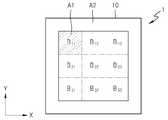
도 1은 본 발명의 일 실시예에 관한 유기 발광 표시 장치를 도시한 개략적인 평면도이고, 도 2는 도 1의 일 화소 블록의 배선 구조를 개략적으로 도시한 도면이다.FIG. 1 is a schematic plan view showing an organic light emitting display according to an embodiment of the present invention, and FIG. 2 is a view schematically showing a wiring structure of one pixel block in FIG.
도 1 및 도 2를 참조하면, 본 실시예에 관한 유기 발광 표시 장치(1)는 기판(10)상에 표시 영역(A1) 및 비표시 영역(A2)이 형성된다.Referring to Figs. 1 and 2, the organic light
표시 영역(A1)은 영상을 표시하는 영역으로서 기판(10)의 중앙을 포함하는 영역에 형성되고, 비표시 영역(A2)은 표시 영역(A1)의 주변에 배치될 수 있다.The display area A1 is formed in an area including the center of the
표시 영역(A1)에는 영상이 구현되는 복수의 화소(P)가 포함된다.The display area A1 includes a plurality of pixels P in which an image is implemented.
각 화소(P)는 제1방향(X)으로 연장된 스캔 배선(S)과, 제1방향(X)에 직교하는 제2방향(Y)으로 연장된 데이터배선(D)으로 정의될 수 있다. 데이터 배선(D)은 비표시 영역(A2)에 구비된 데이터 구동부(미도시)가 제공하는 데이터 신호를 각 화소(P)에 인가하고, 스캔 배선(S)은 비표시 영역(A2)에 구비된 스캔 구동부(미도시)가 제공하는 스캔 신호를 각 화소(P)에 인가한다. 도 2에는 데이터 배선(D)이 제2 방향(Y)으로 연장되고, 스캔 배선(S)이 제1 방향(X)으로 연장된 것으로 도시되어 있으나, 본 발명은 이에 한정되지 않는다. 즉, 데이터 배선(D)과 스캔 배선(S)의 연장 방향은 서로 바뀔 수도 있다.Each pixel P may be defined as a scan line S extending in a first direction X and a data line D extending in a second direction Y perpendicular to the first direction X . The data line D applies a data signal provided by a data driver (not shown) provided in the non-display area A2 to each pixel P, and the scan line S is provided to the non-display area A2 And applies a scan signal provided by a scan driver (not shown) to each pixel P. In FIG. 2, the data line D extends in the second direction Y and the scan line S extends in the first direction X, but the present invention is not limited thereto. That is, the extending direction of the data line D and the scan line S may be mutually different.
각 화소(P)는 제2 방향(Y)으로 연장된 제1 전원 공급선(V1)에 연결된다. 제1 전원 공급선(V1)은 비표시 영역(A2)에 구비된 제1 전원 구동부(미도시)가 제공하는 제1 전원(ELVDD, 도 3 참조)을 각 화소(P)에 인가한다. 한편, 도 2에는 도시되어 있지 않으나, 각 화소(P)는 제2 전원(ELVSS, 도 3 참조)을 공급받는다. 각 화소(P)는 데이터 신호에 대응하여 제1 전원(ELVDD)으로부터 유기 발광 소자(OLED, 도 3 참조)를 경유하여 제2 전원(ELVSS)으로 공급되는 전류량을 제어한다. 그러면, 유기발광소자에서 소정 휘도의 빛이 생성된다.Each pixel P is connected to a first power supply line V1 extending in a second direction Y. The first power supply line V1 applies a first power ELVDD (see FIG. 3) provided by a first power supply unit (not shown) provided in the non-display area A2 to each pixel P. Although not shown in FIG. 2, each pixel P is supplied with a second power ELVSS (see FIG. 3). Each pixel P controls the amount of current supplied from the first power source ELVDD to the second power source ELVSS via the organic light emitting element OLED (see FIG. 3) corresponding to the data signal. Then, light of a predetermined brightness is generated in the organic light emitting element.
도 3은 도 2의 하나의 화소에 대한 회로도이다.3 is a circuit diagram for one pixel in Fig.
도 3을 참조하면, 화소는 유기 발광 소자(organic light emitting device, OLED)와, 유기 발광 소자(OLED)로 전류를 공급하기 위한 화소 회로(C)를 구비한다.Referring to FIG. 3, the pixel includes an organic light emitting device (OLED) and a pixel circuit C for supplying current to the organic light emitting device OLED.
유기 발광 소자(OLED)의 화소 전극은 화소 회로(C)에 접속되고, 대향 전극(20)은 제 2전원(ELVSS)에 접속된다. 유기 발광 소자(OLED)는 화소 회로(C)로부터 공급되는 전류에 대응하여 소정 휘도의 빛을 생성한다.The pixel electrode of the organic light emitting element OLED is connected to the pixel circuit C and the
액티브 매트릭스 방식의 유기 발광 표시 장치는, 적어도 2개의 트랜지스터 및 적어도 1개의 캐패시터를 구비하는데, 구체적으로 데이터 신호를 전달하기 위한 스위칭 트랜지스터, 데이터 신호에 따라 유기 발광 소자를 구동시키기 위한 구동 트랜지스터 및 데이터 전압을 유지시키기 위한 하나의 캐패시터를 포함한다. 여기서, 상기와 같은 박막트랜지스터(21)(23) 및 캐패시터(22)의 개수는 반드시 이에 한정되는 것은 아니며, 이보다 더 많은 수의 박막 트랜지스터(21)(23) 및 캐패시터(22)를 구비할 수 있음은 물론이다.The active matrix type organic light emitting display includes at least two transistors and at least one capacitor. Specifically, the active matrix type organic light emitting display includes a switching transistor for transmitting a data signal, a driving transistor for driving the organic light emitting element according to a data signal, Lt; RTI ID = 0.0 > a < / RTI > capacitor. The number of the thin film transistors 21 and 23 and the number of the
제1 트랜지스터(TR1)의 게이트 전극(214)은 스캔 배선(S)(S, 도 2 참조)에 접속되고, 제1 트랜지스터(TR1)의 제1 전극은 데이터 배선(D, 도 2 참조)에 접속되고, 제1 트랜지스터(TR1)의 제2 전극은 제1 노드(N1)에 접속된다. 즉, 상기 제 1 트랜지스터(TR1)의 게이트 전극(214)에는 스캔 신호(Scan(n))가 입력되고, 제1 트랜지스터(TR1)의 제1 전극으로는 데이터 신호(Data(m))가 입력된다.The
제2 트랜지스터(TR2)의 게이트 전극(214)은 제1 노드(N1)에 접속되고, 제2 트랜지스터(TR2)의 제1 전극은 제1 전원(ELVDD)에 접속되고, 제2 트랜지스터(TR2)의 제2 전극은 유기 발광 소자(OLED)의 화소 전극에 접속된다. 여기서, 상기 제 2 트랜지스터(TR2)는 구동 트랜지스터로서의 역할을 수행한다.The
제1 노드(N1) 및 제2 트랜지스터(TR2)의 제1 전극 즉, 제 1전원(ELVDD) 사이에 제1 캐패시터(Cst)가 접속된다.A first capacitor Cst is connected between a first electrode of the first transistor N1 and the second transistor TR2, that is, the first power source ELVDD.
도 4는 도 1의 유기 발광 표시 장치의 화소의 일부 구성요소를 개략적으로 도시한 단면도이다.FIG. 4 is a cross-sectional view schematically showing a part of a pixel of the organic light emitting diode display of FIG. 1. FIG.
도 4를 참조하면, 기판(10) 상에 구동용 박막트랜지스터인 제2 트랜지스터(TR2), 제1 캐패시터(Cst), 및 유기발광소자(OELD)가 구비되어 있다.Referring to FIG. 4, a second transistor TR2, a first capacitor Cst, and an organic light emitting diode OELD, which are thin film transistors for driving, are provided on a
기판(10)은 SiO2를 주성분으로 하는 투명한 유리 재질로 이루어질 수 있다. 기판(10)은 반드시 이에 한정되는 것은 아니며 투명한 플라스틱 재로 형성할 수도 있다. 유연성이 있는 플렉서블한 기판일 수도 있다. 상기 플렉서블한 기판(10)은 글래스 기판(10)에 비하여 비중이 작아 가볍고, 잘 깨어지지 않으며, 휘어질 수 있는 특성을 가진 소재, 예컨대, 플렉서블 플라스틱 필름과 같은 고분자 소재로 제조하는 것이 바람직하다.The
기판(10) 상에 버퍼층(11)이 더 형성될 수 있다. 상기 버퍼층(11)은 SiOx, SiNx, SiON, AlO, AlON 등의 무기물이나, 아크릴, 폴리이미드 등의 유기물로 이루어지거나, 유기물과 무기물이 교대로 적층될 수 있다. 상기 버퍼층(11)은 산소와 수분을 차단하는 역할을 수행하고, 상기 기판(10)(11)으로부터 발생하는 수분이나, 불순물의 확산을 방지하고, 결정화시 열의 전달 속도를 조절함으로써, 반도체의 결정화가 잘 이루어질 수 있는 역할을 수행한다.A
상기 버퍼층(11)의 상부에는 제2 트랜지스터(TR2)가 형성되어 있다. 본 실시예의 박막 트랜지스터는 바텀 게이트(Bottom gate) 방식의 박막 트랜지스터를 예시하나, 탑 게이트(Top gate) 방식 등 다른 구조의 박막 트랜지스터가 구비될 수 있음은 물론이다.A second transistor TR2 is formed on the
상기 버퍼층(11)의 상부에는 활성층(212)이 형성되어 있다. 상기 활성층(212)이 폴리 실리콘으로 형성될 경우에는 아몰퍼스 실리콘을 형성하고, 이를 결정화시켜 폴리 실리콘으로 변화시키게 된다.An
아몰퍼스 실리콘의 결정화 방법으로는 RTA(Rapid Thermal Annealing)법, SPC(Solid Phase Crystallzation)법, ELA(Eximer Laser Annealing)법, MIC(Metal Induced Crystallization)법, MILC(Metal Induced Lateral Crystallization)법, SLS(Sequential Lateral Solidification)법등 다양한 방법이 적용될 수 있으나, 본 발명에 따른 기판을 적용하기 위해서는 고온의 가열 공정이 요구되지 않는 방법을 이용하는 것이 바람직하다.Examples of the amorphous silicon crystallization method include RTA (Rapid Thermal Annealing), SPC (Solid Phase Crystallization), ELA (Eximer Laser Annealing), MIC (Metal Induced Crystallization), MILC (Metal Induced Lateral Crystallization) Sequential Lateral Solidification) method. However, in order to apply the substrate according to the present invention, it is preferable to use a method that does not require a high-temperature heating process.
예컨대, 저온 폴리 실리콘(Low temperature poly-silicon, LTPS) 공정에 의한 결정화시, 상기 활성층(212)의 활성화를 레이저를 단시간 조사하여 진행함으로써, 기판(10) 이 300℃ 이상의 고온에 노출되는 시간을 제거하여 전체 공정을 300℃ 이하에서 진행가능하다. 이에 따라, 고분자 소재를 적용한 기판(10)을 적용하여 트랜지스터(TR2)를 형성할 수 있다.For example, when crystallization is performed by a low temperature poly-silicon (LTPS) process, the activation of the
상기 활성층(212)에는 N형이나, P형 불순물 이온을 도핑하여 소스 영역(212b)과, 드레인 영역(212a)이 형성되어 있다. 상기 소스 영역(212b)과, 드레인 영역(212a) 사이의 영역은 불순물이 도핑되지 않은 채널 영역(212c)이다.The
상기 활성층(212) 상부에는 게이트 절연막(13)이 형성되어 있다. 상기 게이트 절연막(13)은 SiO2로 된 단일층이나, SiO2와 SiNx의 이중층 구조로 형성되어 있다.A
상기 게이트 절연막(13) 상부의 소정 영역에는 게이트 전극(214)이 형성되어 있다. 상기 게이트 전극(214)은 박막 트랜지스터 온/오프 신호를 인가하는 게이트 라인(미도시)과 연결되어 있다. 상기 게이트 전극(214)은 단일이나, 다중의 도전층으로 형성될 수 있다.A
게이트 전극(214)상에는 층간 절연층(15)을 사이에 두고 활성층(212)의 소스영역(212b) 및 드레인영역(212a)에 각각 접속하는 드레인 전극(216a) 및 소스 전극(216b)이 형성된다. 상기 층간 절연층(15)은 SiO2나, SiNx 등과 같은 절연성 소재로 형성될 수 있으며, 절연성 유기물 등으로도 형성될 수 있다.A
층간 절연층(15) 상에는 드레인 전극(216a) 및 소스 전극(216b)을 덮도록 화소 정의막(18)이 구비된다. 그리고, 버퍼층(11) 및 게이트 절연막(13) 상에 게이트전극(214)과 동일한 투명도전물로 형성된 화소 전극(114)이 형성될 수 있다. 드레인 전극(216a) 및 소스 전극(216b)의 저항은 게이트 전극(214)의 저항보다 작을 수 있다.A
화소 전극(114)는 일 함수가 작은 금속, 즉, Li, Ca, LiF/Ca, LiF/Al, Al, Mg 및 이들의 화합물이 중간층(119) 상에 증착된 후, 그 위에 ITO, IZO, ZnO, In2O3 등의 투명 전극 형성용 물질로 형성된 보조 전극을 형성할 수 있다. 화소 전극(114)는 이에 한정되지 않고, 반사형 전극일 수도 있다.The
화소 전극(114) 상에는 화소 정의막(18)의 일부를 식각하여 중간층(119)이 형성된다. 중간층(119)은 가시 광선을 발광하도록 적어도 유기 발광층을 구비한다.On the
중간층(119) 상에는 공통 전극으로 대향 전극(20)이 형성된다. 상기 중간층(119)에 서로 다른 극성의 전압을 가하여 중간층(119)에서 발광이 이루어지도록 한다.On the
상기 중간층(119)의 유기 발광층은 저분자 유기물이나 고분자 유기물로 구비될 수 있다.The organic light emitting layer of the
상기 중간층(119)의 유기 발광층이 저분자 유기물을 사용할 경우, 상기 중간층(119)은 정공 주입층(Hole injection layer, HIL), 정공 수송층(Hole transport layer, HTL), 유기 발광층(Emissive layer, EML), 전자 수송층(Electron transport layer, ETL), 전자 주입층(Electron injection layer, EIL) 등이 단일이나, 복합의 구조로 적층되어 형성될 수 있다.The
또한, 상기 중간층(119)에 이용 가능한 유기 재료는 구리 프탈로시아닌(Copper phthalocyanine, CuPc), N,N-디(나프탈렌-1-일)-N,N'-디페닐-벤지딘 (N,N'-Di(naphthalene-1-yl)-N,N'-diphenyl-benzidine, NPB), 트리스-8-하이드록시퀴놀린 알루미늄(tris-8-hydroxyquinoline aluminum)(Alq3) 등을 비롯해 다양하게 적용 가능하다. 이들 저분자 유기물은 마스크들을 이용한 진공 증착 등의 방법으로 형성될 수 있다.The organic material that can be used for the
상기 중간층(119)의 유기 발광층이 고분자 유기물을 사용할 경우, 상기 중간층(119)은 정공 수송층(HTL) 및 발광층(EML)을 구비한 구조를 가질 수 있다. 이때, 상기 정공 수송층으로는 PEDOT를 사용하고, 발광층으로는 PPV(Poly-Phenylenevinylene)계 및 폴리플루오렌(Polyfluorene)계 등 고분자 유기물질을 사용한다. 이들 고분자 유기물은 스크린 인쇄법이나 잉크젯 인쇄 방법 등으로 형성할 수 있다.When the organic light emitting layer of the
상기와 같은 중간층(119)은 반드시 이에 한정되는 것은 아니고, 다양한 실시예들이 적용될 수 있음은 물론이다.It is needless to say that the
상기 대향 전극(20)은 화소 전극(114)과 마찬가지로 투명 전극이나, 반사형 전극으로 형성할 수 있다.The
상기 대향 전극(20)이 투명 전극으로 사용될 경우, 상기 대향 전극(20)은 일 함수가 작은 금속, 즉, Li, Ca, LiF/Ca, LiF/Al, Al, Mg 및 이들의 화합물이 중간층(119) 상에 증착된 후, 그 위에 ITO, IZO, ZnO, In2O3 등의 투명 전극 형성용 물질로 형성된 보조 전극을 형성할 수 있다.When the
상기 대향 전극(20)이 반사형 전극으로 사용될 경우, 상기 대향 전극(20)은 Li, Ca, LiF/Ca, LiF/Al, Al, Mg 및 이들의 화합물을 전면 증착하여 형성한다.When the
한편, 상기 화소 전극(114)은 투명 전극이나, 반사형 전극으로 형성시에 각 서브 픽셀의 개구 형태에 대응되는 형태로 형성될 수 있다. 상기 대향 전극(20)은 투명 전극이나, 반사형 전극을 디스플레이 영역 전체에 전면 증착하여 형성될 수 있다. 상기 대향 전극(20)은 반드시 전면 증착될 필요는 없으며, 다양한 패턴으로 형성될 수 있음은 물론이다. 이때, 상기 화소 전극(114)과, 대향 전극(20)은 서로 위치가 반대로 적층될 수 있음은 물론이다.Meanwhile, the
본 실시예에 따른 유기 발광 표시 장치의 경우, 화소 전극(114)은 애노드로 사용되고, 대향 전극(20)은 캐소드로 사용된다. 물론 전극의 극성은 반대로 적용될 수 있음은 물론이다. 도 4에 도시하지 않았으나, 기판(10)의 일 면에 대향하도록 대향 전극(20)의 상부에 밀봉 부재(미도시)가 배치될 수 있다.In the organic light emitting display according to the present embodiment, the
한편, 스캔 배선(S)은 도전층을 이중으로 증착하여 저항을 줄임으로써 신호 및 전압 전달을 용이하게 할 수 있다.On the other hand, the scan wiring S can easily transfer signals and voltages by reducing resistance by doubly depositing a conductive layer.
도 5은 본 발명의 일 실시예에 따른 하나의 화소에 대응하는 스캔 배선의 일 부분을 나타내는 평면도이고, 도 6은 도 5의 Ⅱ-Ⅱ 부분의 단면도이며, 도 7은 도 5의 Ⅲ-Ⅲ 부분의 단면도이다.5 is a plan view showing a part of a scan wiring corresponding to one pixel according to an embodiment of the present invention, FIG. 6 is a cross-sectional view taken along line II-II in FIG. 5, and FIG. 7 is a cross- Fig.
도 5 내지 도 7를 참조하면, 스캔 배선(S)은 버퍼층(11)의 상부에 배치될 수 있다. 구체적으로, 스캔 배선(S)은 게이트 절연막(13)상에 배치되는 제1 도전층(512) 및 제1 도전층(512)과 연결되며 제1 도전층(512)의 위에서부터 기판(10)쪽으로 연장되어 버퍼층(11)상에 배치되는 제2 도전층(516)을 포함할 수 있다.5 to 7, the scan line S may be disposed on the
예를 들어, 제1 도전층(512)은 게이트 절연막(13)상에 배치되고, 제2 도전층(516)은 제1 도전층(512)의 위에서부터 연장되어 버퍼층(11)상에 배치될 수 있다. 그러나, 이에 한정되지 않는다. 제2 도전층(516)은 게이트 절연막(13)상에 배치될 수도 있다. 제2 도전층(516)은 제1 도전층(512)의 위에서부터 대향 전극(20)에 대해 멀어지는 방향으로 연장되는데, 제2 도전층(516)이 제1 도전층(512)에 대해 멀어질수록 제2 도전층(516)은 대향 전극(20)에 대해서도 멀어진다.The first
상기한 제1 도전층(512)은 게이트 전극(214, 도 4 참조)과 동일한 층에 동일한 물질로 형성될 수 있고, 제2 도전층(516)은 소스 및 드레인 전극(212a, 212b, 도 4 참조)과 동일한 물질로 형성될 수 있다.The first
상기한 스캔 배선(S)은 다음과 같이 제조될 수 있다. 기판(10)상에 버퍼층(11), 게이트 절연막(13) 및 도전 물질을 형성한다. 상기한 도전 물질은 게이트 전극(214)과 동일한 층에 동일한 물질로 형성될 수 있다. 그리고, 상기한 도전 물질을 패터닝하여 제1 도전층(512)을 형성할 수 있다.The above-described scan wiring S can be manufactured as follows. A
다음, 게이트 절연막(13)상에 제1 도전층(512)을 덮도록 층간 절연층(13)을 증착한다. 그리고 나서, 제1 도전층(512)의 일부가 노출되도록 층간 절연층(13)을 식각하여 제1 개구(h)를 형성하고, 버퍼층(11)이 노출되도록 게이트 절연막(13) 및 층간 절연층(13)을 식각하여 제2 개구(H)를 형성할 수 있다. 제2 개구(H)는 제1 개구(h)보다 클 수 있다. 다음으로, 제1 도전층(512), 제1 및 제2 개구(h, H)를 덮는 제2 도전층(516)을 증착한다. 제1 개구(h)에 의해 제2 도전층(516)은 제1 도전층(512)과 연결되고, 제2 개구(H)에 의해 제2 도전층(516)의 일부는 제1 도전층(512)보다 아래 층인 버퍼층(11)상에 형성될 수 있다. 상기한 제1 개구(h)는 제1 도전층(512)과 제2 도전층(516)을 연결시키므로 컨택홀이라고 칭할 수 있다.Next, the
이와 같이, 컨택홀을 통해 제1 도전층(512)과 제2 도전층(516)이 전기적으로 연결됨으로써 스캔 배선(S) 전체의 저항을 줄여 신호 및 전압 전달을 용이하게 하는 효과가 있다. 상기한 콘택홀은 하나 이상일 수 있다.As described above, the first
또한, 제2 개구(H)는 제2 도전층(516)의 일부를 제1 도전층(512)보다 아래 층에 형성시킴으로써 대향 전극(20)과 제2 도전층(516)간의 거리를 넓히는 효과가 있다. 그리하여, 대향 전극(20)과 제2 도전층(516)간의 기생 커패시턴스의 증가를 억제할 수 있다. 기생 커패시턴스의 감소를 극대화하기 위해 제2 개구(H)의 크기는 제2 도전층(516)이 제2 개구(H)상에 최대한 많이 형성될 수 있는 크기인 것이 바람직하다.The second opening H is formed by forming a part of the second
한편, 본 실시예에 따른 스캔 배선(S)은 제1 도전층(512)과 제2 도전층(516)의 결합으로 형성되기 때문에 제1 도전층(512)과 제2 도전층(516)의 중첩 영역을 최소화하여 하여 기생 커패시턴의 증가를 억제할 수 있다.Since the scan wiring S according to the present embodiment is formed by the combination of the first
도 8은 본 발명의 다른 실시예에 따른 하나의 화소에 대응하는 스캔 배선의 일 부분을 나타내는 평면도이다. 도 8에 도시된 바와 같이, 제1 도전층(512)은 게이트 절연막(13) 상에 이격 배치되는 제1 서브 도전층(512a) 및 제2 서브 도전층(b)을 포함할 수 있다. 그리고, 제2 도전층(516)은 제1 서브 도전층(512a) 및 제2 서브 도전층(512b)이 연결되도록 형성될 수 있다. 예를 들어, 제2 도전층(516)은 제1 서브 제2 서브 도전층(512a, 512b) 각각의 제1 개구(h)와 제2 개구(H)를 채우면서 형성될 수 있다.8 is a plan view showing a part of a scan wiring corresponding to one pixel according to another embodiment of the present invention. 8, the first
이와 같은 스캔 배선(S)은 다음과 같이 제조될 수 있다. 기판(10)상에 버퍼층(11), 게이트 절연막(13) 및 도전 물질을 형성한다. 상기한 도전 물질은 게이트 전극(214)과 동일한 층에 동일한 물질로 형성될 수 있다. 그리고, 상기한 도전 물질을 패터닝하여 제1 및 제2 서브 도전층(512a, 512b)을 형성할 수 있다.Such a scan wiring S can be manufactured as follows. A
다음, 게이트 절연막(13)상에 제1 및 제2 서브 도전층(512a, 512b)을 덮도록 층간 절연층(13)을 증착한다. 그리고 나서, 제1 및 제2 서브 도전층(512a, 512b) 각각의 일부가 노출되도록 제1 및 제2 서브 도전층(512a, 512b) 각각의 상부에 증착된 층간 절연층(13)을 식각하여 제1 개구(h)를 패터닝한다. 뿐만 아니라, 버퍼층(11)이 노출되도록 게이트 절연막(13) 및 층간 절연층(13)을 식각하여 제2 개구(H)를 형성할 수 있다. 제2 개구(H)는 제1 개구(h)보다 클 수 있다. 다음으로, 제1 및 제2 서브 도전층(512a, 512b), 제1 및 제2 개구(h, H)를 덮는 제2 도전층(516)을 증착한다. 제1 개구(h)에 의해 제2 도전층(516)은 제1 및 제2 서브 도전층(512a, 512b)과 연결되고, 제2 개구(H)에 의해 제2 도전층(516)의 일부는 제1 및 제2 서브 도전층(512a, 512b)보다 아래 층에 형성될 수 있다. 본 실시예에서 제1 도전층(512)가 두 개의 서브 도전층(512a, 512b)로 형성된다고 하였으나, 이에 한정되지 않는다. 서브 도전층은 3개 이상일 수도 있다.Next, the
뿐만 아니라, 제2 개구(H)를 제2 도전층(516)의 크기이상으로 하여 기생 커패시턴스의 감소를 극대화할 수도 있다.In addition, the second opening H can be made larger than the size of the second
도 9는 본 발명의 또 다른 실시예에 따른 하나의 화소에 대응하는 스캔 배선(S)의 일 부분을 나타내는 평면도이고, 도 10는 도 9의 Ⅳ-Ⅳ부분의 단면도이다. 도 9 및 도 10에 도시된 바와 같이, 제1 도전층(512)은 게이트 절연막(13) 상에 이격 배치되는 제1 서브 도전층(512a) 및 제2 서브 도전층(512b)을 포함할 수 있다. 그리고, 제1 서브 도전층(512a) 및 제2 서브 도전층(512b)의 일부가 제1 개구(h) 내에 포함되도록 게이트 절연막(13) 및 층간 절연층(13)을 식각한다. 그리고, 상기한 제2 개구(H)상에 제2 도전층(516)을 형성한다. 이와 같이, 제2 개구(H)내에 제1 서브 도전층(512a) 및 제2 서브 도전층(512b)의 일부가 포함되고, 상기한 제2 개구(H) 상에 제2 도전층(516)이 형성되기 때문에 제1 개구(h)를 형성할 필요가 없다.FIG. 9 is a plan view showing a part of a scan line S corresponding to one pixel according to another embodiment of the present invention, and FIG. 10 is a cross-sectional view of a portion IV-IV of FIG. 9 and 10, the first
이와 같이 스캔 배선(S)을 다중의 도전층으로 형성함으로써 스캔 배선(S) 전체의 저항을 감소시킬 수 있을 뿐만 아니라, 제2 도전층(516)을 대향 전극(20)과 멀어지도록 배치시킴으로써 기생 커패시턴스를 감소시킬 수 있다.By forming the scan interconnections S as multiple conductive layers as described above, the resistance of the entire scan interconnections S can be reduced. In addition, by disposing the second
도면에는 게이트 절연막(13)의 제2 개구(H)와 층간 절연층(13)의 제2 개구(H)가 동일한 크기인 것으로 도시되어 있으나, 이에 한정되지 않는다. 층간 절연층(13)의 제2 개구(H)는 게이트 절연막(13)의 제2 개구(H)이하일 수 있다. 또한, 층간 절연층(13)에만 제2 개구(H)가 형성되고 게이트 절연막(13)에는 제2 개구(H)가 형성되지 않을 수도 있다.In the figure, the second opening H of the
상기한 배선 구조는 스캔 배선 뿐만 아니라 데이터 배선에도 적용될 수 있다. 본 발명은 도면에 도시된 실시예를 참고로 설명되었으나 이는 예시적인 것에 불과하며, 당해 기술 분야에서 통상의 지식을 가진 자라면 이로부터 다양한 변형 및 균등한 다른 실시예가 가능하다는 점을 이해할 것이다. 따라서, 본 발명의 진정한 기술적 보호 범위는 첨부된 특허청구범위의 기술적 사상에 의하여 정해져야 할 것이다.The above-described wiring structure can be applied not only to the scan wiring but also to the data wiring. While the present invention has been described with reference to exemplary embodiments, it is to be understood that the invention is not limited to the disclosed exemplary embodiments, but, on the contrary, is intended to cover various modifications and equivalent arrangements included within the spirit and scope of the invention. Accordingly, the true scope of the present invention should be determined by the technical idea of the appended claims.
10 : 기판 11 : 버퍼층
13: 게이트 절연막 15: 층간 절연층
18: 화소 정의막 20: 대향 전극
S : 스캔 배선 512: 제1 도전층
512a: 제1 서브 도전층 512b: 제2 서브 도전층
h : 제1 개구 H: 제2 개구10: substrate 11: buffer layer
13: gate insulating film 15: interlayer insulating layer
18: pixel defining film 20: counter electrode
S: scan wiring 512: first conductive layer
512a: first
h: first opening H: second opening
Claims (20)
Translated fromKorean상기 제1 방향과 교차하는 제2 방향으로 연장된 복수 개의 제2 배선들;을 포함하고,
상기 제1 배선들 중 적어도 하나는 제1 도전층, 및 상기 제1 도전층 상의 제2 도전층을 포함하며,
상기 제2 도전층은 상기 제1 도전층의 위에서부터 상기 제1 도전층과 동일한 층 상으로 또는 그 아래 층 상으로 연장되되, 상기 제2 도전층 중 상기 제1 도전층의 위의 제1 부분은 상기 제1 도전층과 직접 접촉하고, 상기 제1 도전층과 동일한 층 상으로 또는 그 아래 층 상으로 연장된 상기 제2 도전층의 제2 부분의 바닥면은 상기 제2 부분 아래에 위치하는 절연층과 직접 접촉하는, 유기 발광 표시 장치.A plurality of first wirings extending in a first direction; And
And a plurality of second wirings extending in a second direction intersecting with the first direction,
Wherein at least one of the first wirings includes a first conductive layer and a second conductive layer on the first conductive layer,
Wherein the second conductive layer extends from above the first conductive layer onto or on the same layer as the first conductive layer, wherein a first portion of the second conductive layer above the first conductive layer Is in direct contact with the first conductive layer and a bottom surface of the second portion of the second conductive layer extending on or under the same layer as the first conductive layer is located below the second portion Wherein the organic layer is in direct contact with the insulating layer.
상기 제1 배선들과 상기 제2 배선들은 교차하여 복수 개의 화소들을 정의하며,
상기 복수 개의 화소들 각각은
화소 전극, 유기 발광층을 구비하는 중간층 및 대향 전극을 구비하는 유기발광소자과 게이트 전극, 소스 및 드레인 전극을 구비하는 스위칭소자를 포함하고,
상기 제2 도전층의 상기 제2 부분은 상기 제1 부분 보다 상기 대향 전극으로부터 먼 유기 발광 표시 장치.
The method according to claim 1,
The first wirings and the second wirings intersect to define a plurality of pixels,
Each of the plurality of pixels
An organic light emitting element having a pixel electrode, an intermediate layer having an organic light emitting layer and a counter electrode, a gate electrode, and a switching element having a source and a drain electrode,
And the second portion of the second conductive layer is farther from the counter electrode than the first portion.
상기 제1 배선들은 상기 화소들에 주사 신호를 공급하는 스캔 배선들인 유기 발광 표시 장치.3. The method of claim 2,
Wherein the first wirings are scan wirings for supplying a scan signal to the pixels.
기판; 및
상기 기판 상에 배치된 버퍼층;을 더 포함하고,
상기 버퍼층 위에 상기 제1 배선들 및 상기 제2 배선들이 형성된 유기 발광 표시 장치.The method according to claim 1,
Board; And
And a buffer layer disposed on the substrate,
Wherein the first wirings and the second wirings are formed on the buffer layer.
상기 제2 도전층의 상기 제2 부분은 상기 버퍼층 상에 형성된 유기 발광 표시 장치.6. The method of claim 5,
And the second portion of the second conductive layer is formed on the buffer layer.
상기 버퍼층과 상기 제1 도전층 사이에 형성된 제1 절연층;을 더 포함하는 유기 발광 표시 장치.6. The method of claim 5,
And a first insulating layer formed between the buffer layer and the first conductive layer.
상기 제1 절연층은 상기 제2 도전층의 상기 제2 부분이 상기 버퍼층과 접촉하도록 제1 개구를 구비하는 유기 발광 표시 장치.8. The method of claim 7,
Wherein the first insulating layer has a first opening so that the second portion of the second conductive layer contacts the buffer layer.
상기 제1 절연층 상에 배치되며, 상기 제1 도전층을 덮는 제2 절연층;을 더 포함하는 유기 발광 표시 장치.8. The method of claim 7,
And a second insulating layer disposed on the first insulating layer and covering the first conductive layer.
상기 제2 절연층은 상기 제2 도전층의 상기 제2 부분이 상기 버퍼층 또는 상기 제1 절연층과 접촉하도록 제2 개구를 포함하는, 유기 발광 표시 장치.10. The method of claim 9,
And the second insulating layer includes a second opening so that the second portion of the second conductive layer is in contact with the buffer layer or the first insulating layer.
상기 제1 도전층의 상기 제1 부분은과 상기 제2 도전층은 상기 제2 절연층에 형성된 컨택홀을 통해 연결된 유기 발광 표시 장치.10. The method of claim 9,
Wherein the first portion of the first conductive layer and the second conductive layer are connected through a contact hole formed in the second insulating layer.
상기 제2 도전층의 상기 제1 부분은 상기 제1 도전층의 일부를 덮으면서 상기 제2 부분은 상기 버퍼층 상에 배치되는 유기 발광 표시 장치.6. The method of claim 5,
Wherein the first portion of the second conductive layer covers a portion of the first conductive layer and the second portion is disposed on the buffer layer.
상기 제1 도전층은 상기 게이트 전극과 동일한 층에 형성된 유기 발광 표시 장치.3. The method of claim 2,
Wherein the first conductive layer is formed in the same layer as the gate electrode.
상기 제1 도전층은 상기 게이트 전극과 동일한 물질로 형성된 유기 발광 표시 장치.3. The method of claim 2,
Wherein the first conductive layer is formed of the same material as the gate electrode.
상기 제2 도전층은 상기 소스 및 드레인 전극과 동일한 물질로 형성된 유기 발광 표시 장치.3. The method of claim 2,
And the second conductive layer is formed of the same material as the source and drain electrodes.
상기 제1 도전층은 상호 이격 배치되는 복수 개의 서브 도전층을 포함하는 유기 발광 표시 장치.The method according to claim 1,
Wherein the first conductive layer comprises a plurality of sub-conductive layers spaced apart from each other.
상기 복수 개의 서브 도전층 각각은 상기 제2 도전층과 연결된 유기 발광 표시 장치.17. The method of claim 16,
And each of the plurality of sub conductive layers is connected to the second conductive layer.
상기 제2 도전층은 상기 복수 개의 서브 도전층 각각의 일부를 덮는 유기 발광 표시 장치.17. The method of claim 16,
And the second conductive layer covers a part of each of the plurality of sub conductive layers.
상기 복수 개의 서브 도전층 사이의 상기 제2 도전층의 상기 제2 부분은 상기 복수의 서브 도전층과 동일한 층 또는 그 아래의 층에 배치된 유기 발광 표시 장치.17. The method of claim 16,
And the second portion of the second conductive layer between the plurality of sub conductive layers is disposed in the same layer as or below the plurality of sub conductive layers.
상기 화소들 각각에 연결되고, 상기 화소들에 주사 신호를 공급하는 복수의 스캔 배선들; 및
상기 화소들 각각에 연결되고, 상기 화소들에 데이터 신호를 공급하는 복수의 데이터 배선들;을 포함하고,
상기 스캔 배선들 중 적어도 하나는 제1 도전층, 및 상기 제1 도전층 상의 제2 도전층을 포함하며,
상기 제2도전층 중 상기 제1 도전층의 위의 제1 부분은 상기 제1 도전층과 직접 접촉하고, 상기 제1 도전층과 동일한 층 상으로 또는 그 아래 층 상으로 연장된 상기 제2도전층의 제2 부분의 바닥면은 상기 제2 부분 아래에 위치하는 절연층의 상면과 직접 접촉하며, 상기 제2 부분은 상기 제1 부분 보다 상기 대향 전극에 대해 멀어지는 방향에 위치하는 유기 발광 표시 장치.A plurality of pixels including an organic light emitting element having a pixel electrode, an intermediate layer having an organic light emitting layer and a counter electrode, a gate electrode, and a switching element having a source and a drain electrode;
A plurality of scan lines connected to each of the pixels and supplying a scan signal to the pixels; And
A plurality of data lines connected to each of the pixels and supplying a data signal to the pixels,
Wherein at least one of the scan lines includes a first conductive layer and a second conductive layer on the first conductive layer,
Wherein a first portion of the second conductive layer overlying the first conductive layer is in direct contact with the first conductive layer and the second conductive layer extends over or on the same layer as the first conductive layer, Wherein a bottom surface of the second portion of the layer directly contacts an upper surface of the insulating layer located below the second portion and the second portion is located in a direction away from the counter electrode, .
Priority Applications (2)
| Application Number | Priority Date | Filing Date | Title |
|---|---|---|---|
| KR1020120115610AKR101965256B1 (en) | 2012-10-17 | 2012-10-17 | Organic light emitting display device and the manufacturing method thereof |
| US13/827,231US9349978B2 (en) | 2012-10-17 | 2013-03-14 | Organic light emitting display device and method of manufacturing the same |
Applications Claiming Priority (1)
| Application Number | Priority Date | Filing Date | Title |
|---|---|---|---|
| KR1020120115610AKR101965256B1 (en) | 2012-10-17 | 2012-10-17 | Organic light emitting display device and the manufacturing method thereof |
Publications (2)
| Publication Number | Publication Date |
|---|---|
| KR20140049401A KR20140049401A (en) | 2014-04-25 |
| KR101965256B1true KR101965256B1 (en) | 2019-04-04 |
Family
ID=50474573
Family Applications (1)
| Application Number | Title | Priority Date | Filing Date |
|---|---|---|---|
| KR1020120115610AActiveKR101965256B1 (en) | 2012-10-17 | 2012-10-17 | Organic light emitting display device and the manufacturing method thereof |
Country Status (2)
| Country | Link |
|---|---|
| US (1) | US9349978B2 (en) |
| KR (1) | KR101965256B1 (en) |
Families Citing this family (3)
| Publication number | Priority date | Publication date | Assignee | Title |
|---|---|---|---|---|
| KR102101644B1 (en) | 2014-05-12 | 2020-04-17 | 엘지디스플레이 주식회사 | Organic light emitting device and method for manufacturing the same |
| KR101954821B1 (en) | 2014-05-12 | 2019-05-31 | 엘지디스플레이 주식회사 | Organic light emitting device |
| WO2025160763A1 (en)* | 2024-01-30 | 2025-08-07 | 京东方科技集团股份有限公司 | Display substrate and display apparatus |
Citations (2)
| Publication number | Priority date | Publication date | Assignee | Title |
|---|---|---|---|---|
| JP2005331902A (en) | 2004-04-21 | 2005-12-02 | Sharp Corp | Active matrix substrate for display device and manufacturing method thereof |
| US8067775B2 (en) | 2008-10-24 | 2011-11-29 | Semiconductor Energy Laboratory Co., Ltd. | Thin film transistor with two gate electrodes |
Family Cites Families (28)
| Publication number | Priority date | Publication date | Assignee | Title |
|---|---|---|---|---|
| JPH08250488A (en)* | 1995-01-13 | 1996-09-27 | Seiko Epson Corp | Plasma processing apparatus and method |
| JPH10135270A (en)* | 1996-10-31 | 1998-05-22 | Casio Comput Co Ltd | Semiconductor device and manufacturing method thereof |
| US5812403A (en)* | 1996-11-13 | 1998-09-22 | Applied Materials, Inc. | Methods and apparatus for cleaning surfaces in a substrate processing system |
| JP4095731B2 (en)* | 1998-11-09 | 2008-06-04 | 株式会社ルネサステクノロジ | Semiconductor device manufacturing method and semiconductor device |
| WO2000077844A1 (en)* | 1999-06-15 | 2000-12-21 | Fujikura Ltd. | Semiconductor package, semiconductor device, electronic device, and method of manufacturing semiconductor package |
| JP3996315B2 (en)* | 2000-02-21 | 2007-10-24 | 松下電器産業株式会社 | Semiconductor device and manufacturing method thereof |
| JP3985899B2 (en)* | 2002-03-28 | 2007-10-03 | 株式会社日立国際電気 | Substrate processing equipment |
| JP3855081B2 (en)* | 2002-07-01 | 2006-12-06 | 株式会社日立国際電気 | CVD apparatus equipped with fluorine gas cleaning mechanism and method of cleaning CVD apparatus with fluorine gas |
| JP2004318093A (en)* | 2003-03-31 | 2004-11-11 | Sanyo Electric Co Ltd | Light emitting display, its driving method, electroluminescent display circuit, and electroluminescent display |
| US7701069B2 (en)* | 2003-06-30 | 2010-04-20 | Intel Corporation | Solder interface locking using unidirectional growth of an intermetallic compound |
| WO2008035678A1 (en)* | 2006-09-19 | 2008-03-27 | Tokyo Electron Limited | Plasma cleaning process and plasma cvd method |
| KR101288116B1 (en) | 2006-12-19 | 2013-07-18 | 엘지디스플레이 주식회사 | An Array Substrate of Poly-Silicon Liquid Crystal Display Device and the method for fabricating thereof |
| US7897971B2 (en)* | 2007-07-26 | 2011-03-01 | Semiconductor Energy Laboratory Co., Ltd. | Display device |
| KR100967933B1 (en) | 2008-07-09 | 2010-07-06 | 주식회사 에스에프에이 | Functional film attachment system and method |
| US8227278B2 (en)* | 2008-09-05 | 2012-07-24 | Semiconductor Energy Laboratory Co., Ltd. | Methods for manufacturing thin film transistor and display device |
| KR101914404B1 (en) | 2008-11-21 | 2018-11-01 | 가부시키가이샤 한도오따이 에네루기 켄큐쇼 | Semiconductor device |
| KR101570347B1 (en)* | 2008-11-25 | 2015-11-20 | 삼성디스플레이 주식회사 | film transistor array panel and manufacturing Method thereof |
| KR101518318B1 (en) | 2008-12-10 | 2015-05-07 | 삼성디스플레이 주식회사 | Thin film transistor array panel and method for manufacturing the same |
| KR102097932B1 (en)* | 2009-07-31 | 2020-04-06 | 가부시키가이샤 한도오따이 에네루기 켄큐쇼 | Semiconductor device and manufacturing method thereof |
| US8324738B2 (en)* | 2009-09-01 | 2012-12-04 | Taiwan Semiconductor Manufacturing Company, Ltd. | Self-aligned protection layer for copper post structure |
| KR20110038931A (en)* | 2009-10-09 | 2011-04-15 | 엘지디스플레이 주식회사 | Display device and manufacturing method |
| US8659155B2 (en)* | 2009-11-05 | 2014-02-25 | Taiwan Semiconductor Manufacturing Company, Ltd. | Mechanisms for forming copper pillar bumps |
| KR20110068653A (en)* | 2009-12-16 | 2011-06-22 | 엘지디스플레이 주식회사 | Display |
| TWM397597U (en)* | 2010-04-15 | 2011-02-01 | Di-Quan Hu | Package structure of integrated circuit |
| US20130194528A1 (en)* | 2010-08-06 | 2013-08-01 | Wintek Corporation | Display structure |
| TW201211622A (en)* | 2010-08-06 | 2012-03-16 | Wintek Corp | Display structure |
| KR101348537B1 (en) | 2010-09-29 | 2014-01-07 | 파나소닉 주식회사 | El display panel, el display device and method for manufacturing el display panel |
| KR102080065B1 (en)* | 2013-04-30 | 2020-04-07 | 엘지디스플레이 주식회사 | Thin film transistor array substrate and method for fabricating the same |
- 2012
- 2012-10-17KRKR1020120115610Apatent/KR101965256B1/enactiveActive
- 2013
- 2013-03-14USUS13/827,231patent/US9349978B2/enactiveActive
Patent Citations (2)
| Publication number | Priority date | Publication date | Assignee | Title |
|---|---|---|---|---|
| JP2005331902A (en) | 2004-04-21 | 2005-12-02 | Sharp Corp | Active matrix substrate for display device and manufacturing method thereof |
| US8067775B2 (en) | 2008-10-24 | 2011-11-29 | Semiconductor Energy Laboratory Co., Ltd. | Thin film transistor with two gate electrodes |
Also Published As
| Publication number | Publication date |
|---|---|
| US9349978B2 (en) | 2016-05-24 |
| KR20140049401A (en) | 2014-04-25 |
| US20140103304A1 (en) | 2014-04-17 |
Similar Documents
| Publication | Publication Date | Title |
|---|---|---|
| KR100573132B1 (en) | Organic electroluminescent display and manufacturing method thereof | |
| KR100592273B1 (en) | Flat panel display device | |
| US7420212B2 (en) | Flat panel display | |
| US9006717B2 (en) | Organic light-emitting display apparatus and method of manufacturing organic light-emitting display apparatus | |
| KR102056865B1 (en) | The film for a display apparatus, The organic light emitting display device comprising the film and the manufacturing method thereof | |
| KR100553745B1 (en) | Flat Panel Display | |
| KR100647599B1 (en) | Organic electroluminescent display and manufacturing method thereof | |
| KR20130053053A (en) | Organic light emitting display apparatus and method of manufacturing organic light emitting display apparatus | |
| KR20140020565A (en) | Organic light emitting display apparatus and method of manufacturing organic light emitting display apparatus | |
| KR102116493B1 (en) | Organinc light emitting display device and manufacturing method for the same | |
| KR20120063746A (en) | Organinc light emitting display device and manufacturing method for the same | |
| US20150060784A1 (en) | Organic light emitting display and method for manufacturing the same | |
| KR20120016783A (en) | Organic light emitting display device and manufacturing method thereof | |
| US20060103290A1 (en) | Organic electroluminescence device and method of manufacturing the same | |
| KR100573154B1 (en) | Electroluminescent display device and manufacturing method thereof | |
| KR20140046519A (en) | Organic light emitting diode display | |
| KR20060106209A (en) | Light-emitting display device and manufacturing method | |
| KR101965256B1 (en) | Organic light emitting display device and the manufacturing method thereof | |
| KR100683679B1 (en) | Organic light emitting device | |
| KR100813841B1 (en) | Organic light emitting display device | |
| KR100719599B1 (en) | Flat panel display device | |
| KR100658755B1 (en) | OLED display and manufacturing method thereof | |
| KR100787458B1 (en) | Organic light emitting display device | |
| KR100669709B1 (en) | Organic electroluminescent display and manufacturing method | |
| KR20140105296A (en) | The apparatus for mounting a device and The method for mounting a device |
Legal Events
| Date | Code | Title | Description |
|---|---|---|---|
| PA0109 | Patent application | Patent event code:PA01091R01D Comment text:Patent Application Patent event date:20121017 | |
| PG1501 | Laying open of application | ||
| A201 | Request for examination | ||
| PA0201 | Request for examination | Patent event code:PA02012R01D Patent event date:20171016 Comment text:Request for Examination of Application Patent event code:PA02011R01I Patent event date:20121017 Comment text:Patent Application | |
| E902 | Notification of reason for refusal | ||
| PE0902 | Notice of grounds for rejection | Comment text:Notification of reason for refusal Patent event date:20180918 Patent event code:PE09021S01D | |
| E701 | Decision to grant or registration of patent right | ||
| PE0701 | Decision of registration | Patent event code:PE07011S01D Comment text:Decision to Grant Registration Patent event date:20181230 | |
| PR0701 | Registration of establishment | Comment text:Registration of Establishment Patent event date:20190328 Patent event code:PR07011E01D | |
| PR1002 | Payment of registration fee | Payment date:20190329 End annual number:3 Start annual number:1 | |
| PG1601 | Publication of registration | ||
| PR1001 | Payment of annual fee | Payment date:20220302 Start annual number:4 End annual number:4 | |
| PR1001 | Payment of annual fee | Payment date:20250224 Start annual number:7 End annual number:7 |