KR101962819B1 - Image display device intgrated with antenna and antenna for image display device - Google Patents
Image display device intgrated with antenna and antenna for image display deviceDownload PDFInfo
- Publication number
- KR101962819B1 KR101962819B1KR1020180026380AKR20180026380AKR101962819B1KR 101962819 B1KR101962819 B1KR 101962819B1KR 1020180026380 AKR1020180026380 AKR 1020180026380AKR 20180026380 AKR20180026380 AKR 20180026380AKR 101962819 B1KR101962819 B1KR 101962819B1
- Authority
- KR
- South Korea
- Prior art keywords
- transmission line
- image display
- antenna
- circuit board
- printed circuit
- Prior art date
- Legal status (The legal status is an assumption and is not a legal conclusion. Google has not performed a legal analysis and makes no representation as to the accuracy of the status listed.)
- Active
Links
- 230000005540biological transmissionEffects0.000claimsabstractdescription83
- 239000000758substrateSubstances0.000claimsdescription17
- 238000005538encapsulationMethods0.000claimsdescription9
- 230000005855radiationEffects0.000claimsdescription8
- 230000002093peripheral effectEffects0.000claimsdescription6
- 239000010409thin filmSubstances0.000claimsdescription6
- 238000000034methodMethods0.000claims2
- 239000010410layerSubstances0.000description53
- 239000011810insulating materialSubstances0.000description7
- 239000003990capacitorSubstances0.000description6
- 230000003287optical effectEffects0.000description5
- 239000011347resinSubstances0.000description5
- 229920005989resinPolymers0.000description5
- 238000004891communicationMethods0.000description4
- 239000002184metalSubstances0.000description4
- 239000010408filmSubstances0.000description3
- 230000006870functionEffects0.000description3
- 239000004973liquid crystal related substanceSubstances0.000description3
- 239000004925Acrylic resinSubstances0.000description2
- 229920000178Acrylic resinPolymers0.000description2
- 229910052581Si3N4Inorganic materials0.000description2
- VYPSYNLAJGMNEJ-UHFFFAOYSA-NSilicium dioxideChemical compoundO=[Si]=OVYPSYNLAJGMNEJ-UHFFFAOYSA-N0.000description2
- 229910045601alloyInorganic materials0.000description2
- 239000000956alloySubstances0.000description2
- 230000000052comparative effectEffects0.000description2
- 238000005516engineering processMethods0.000description2
- 150000003949imidesChemical class0.000description2
- 238000010295mobile communicationMethods0.000description2
- 230000035945sensitivityEffects0.000description2
- HQVNEWCFYHHQES-UHFFFAOYSA-Nsilicon nitrideChemical compoundN12[Si]34N5[Si]62N3[Si]51N64HQVNEWCFYHHQES-UHFFFAOYSA-N0.000description2
- 229910052814silicon oxideInorganic materials0.000description2
- 238000002834transmittanceMethods0.000description2
- 239000012790adhesive layerSubstances0.000description1
- 230000015556catabolic processEffects0.000description1
- 238000006731degradation reactionMethods0.000description1
- 239000003822epoxy resinSubstances0.000description1
- 239000011521glassSubstances0.000description1
- 239000000463materialSubstances0.000description1
- 229910044991metal oxideInorganic materials0.000description1
- 150000004706metal oxidesChemical class0.000description1
- 229920000647polyepoxidePolymers0.000description1
- 229920000728polyesterPolymers0.000description1
- 238000004904shorteningMethods0.000description1
- 230000008054signal transmissionEffects0.000description1
- 229910000679solderInorganic materials0.000description1
- 125000006850spacer groupChemical group0.000description1
- 125000003011styrenyl groupChemical class[H]\C(*)=C(/[H])C1=C([H])C([H])=C([H])C([H])=C1[H]0.000description1
Images


Classifications
- H—ELECTRICITY
- H01—ELECTRIC ELEMENTS
- H01Q—ANTENNAS, i.e. RADIO AERIALS
- H01Q21/00—Antenna arrays or systems
- H01Q21/0006—Particular feeding systems
- H—ELECTRICITY
- H01—ELECTRIC ELEMENTS
- H01Q—ANTENNAS, i.e. RADIO AERIALS
- H01Q1/00—Details of, or arrangements associated with, antennas
- H01Q1/36—Structural form of radiating elements, e.g. cone, spiral, umbrella; Particular materials used therewith
- H01Q1/38—Structural form of radiating elements, e.g. cone, spiral, umbrella; Particular materials used therewith formed by a conductive layer on an insulating support
- H—ELECTRICITY
- H01—ELECTRIC ELEMENTS
- H01Q—ANTENNAS, i.e. RADIO AERIALS
- H01Q1/00—Details of, or arrangements associated with, antennas
- H01Q1/12—Supports; Mounting means
- H01Q1/22—Supports; Mounting means by structural association with other equipment or articles
- H01Q1/24—Supports; Mounting means by structural association with other equipment or articles with receiving set
- H01Q1/241—Supports; Mounting means by structural association with other equipment or articles with receiving set used in mobile communications, e.g. GSM
- H01Q1/242—Supports; Mounting means by structural association with other equipment or articles with receiving set used in mobile communications, e.g. GSM specially adapted for hand-held use
- H01Q1/243—Supports; Mounting means by structural association with other equipment or articles with receiving set used in mobile communications, e.g. GSM specially adapted for hand-held use with built-in antennas
- H—ELECTRICITY
- H01—ELECTRIC ELEMENTS
- H01Q—ANTENNAS, i.e. RADIO AERIALS
- H01Q1/00—Details of, or arrangements associated with, antennas
- H01Q1/44—Details of, or arrangements associated with, antennas using equipment having another main function to serve additionally as an antenna, e.g. means for giving an antenna an aesthetic aspect
- H01Q1/46—Electric supply lines or communication lines
- H—ELECTRICITY
- H04—ELECTRIC COMMUNICATION TECHNIQUE
- H04M—TELEPHONIC COMMUNICATION
- H04M1/00—Substation equipment, e.g. for use by subscribers
- H04M1/02—Constructional features of telephone sets
- H04M1/0202—Portable telephone sets, e.g. cordless phones, mobile phones or bar type handsets
- H04M1/0249—Details of the mechanical connection between the housing parts or relating to the method of assembly
- H—ELECTRICITY
- H04—ELECTRIC COMMUNICATION TECHNIQUE
- H04M—TELEPHONIC COMMUNICATION
- H04M1/00—Substation equipment, e.g. for use by subscribers
- H04M1/02—Constructional features of telephone sets
- H04M1/0202—Portable telephone sets, e.g. cordless phones, mobile phones or bar type handsets
- H04M1/026—Details of the structure or mounting of specific components
- H04M1/0266—Details of the structure or mounting of specific components for a display module assembly
- H—ELECTRICITY
- H04—ELECTRIC COMMUNICATION TECHNIQUE
- H04M—TELEPHONIC COMMUNICATION
- H04M1/00—Substation equipment, e.g. for use by subscribers
- H04M1/02—Constructional features of telephone sets
- H04M1/0202—Portable telephone sets, e.g. cordless phones, mobile phones or bar type handsets
- H04M1/026—Details of the structure or mounting of specific components
- H04M1/0277—Details of the structure or mounting of specific components for a printed circuit board assembly
Landscapes
- Engineering & Computer Science (AREA)
- Signal Processing (AREA)
- Computer Networks & Wireless Communication (AREA)
- Devices For Indicating Variable Information By Combining Individual Elements (AREA)
- Liquid Crystal (AREA)
Abstract
Translated fromKoreanDescription
Translated fromKorean본 발명은 안테나가 결합된 화상 표시 장치 및 화상 표시 장치용 안테나에 관한 것이다.The present invention relates to an image display apparatus to which an antenna is coupled and an antenna for an image display apparatus.
최근 정보화 사회가 발전함에 따라 와이 파이(Wi-Fi), 블루투스(Bluetooth) 등과 같은 무선 통신 기술이 디스플레이 장치와 결합되어, 예를 들면 스마트폰 형태로 구현되고 있다. 이 경우, 안테나가 상기 디스플레이 장치에 결합되어 통신 기능이 수행될 수 있다.BACKGROUND ART [0002] With the development of an information society in recent years, wireless communication technologies such as Wi-Fi and Bluetooth have been combined with a display device, for example, in the form of a smart phone. In this case, an antenna may be coupled to the display device to perform a communication function.
최근 이동통신 기술이 진화하면서, 초고주파 대역의 통신을 수행하기 위한 안테나가 상기 디스플레이 장치에 결합될 필요가 있다. 또한, 하나의 디스플레이 장치에 구현되는 통신 기능이 증가함에 따라, 서로 다른 주파수에 감도를 갖는 복수의 안테나들이 상기 디스플레이 장치에 결합될 수 있다.Recently, as the mobile communication technology evolves, an antenna for performing communication in a very high frequency band needs to be coupled to the display device. In addition, as the communication function implemented in one display device increases, a plurality of antennas having sensitivity at different frequencies can be coupled to the display device.
상기 복수의 안테나들은 전송 선로와 같은 안테나 배선들에 의해 서로 연결된다. 그러나, 상기 디스플레이 장치에 각종 구동 회로 칩, 메모리 장치, 센서 칩 등이 집적화됨에 따라, 상기 안테나 배선들이 배열될 수 있는 공간 또는 면적이 감소된다. 이에 따라, 상기 안테나 배선 경로가 우회되거나 길이가 증가하여, 신호 저항을 증가시킬 수 있다.The plurality of antennas are connected to each other by antenna wirings such as a transmission line. However, as various driving circuit chips, memory devices, sensor chips, and the like are integrated in the display device, the space or area in which the antenna wirings can be arranged is reduced. Thus, the antenna wiring path can be bypassed or the length can be increased, and the signal resistance can be increased.
또한, 상기 디스플레이 장치에는 레지스터, 커패시터, 콘덴서 등과 같은 각종 회로 구조물들이 포함되며, 상기 회로 구조물에 의해 발생하는 노이즈에 의해 안테나 신호가 간섭 또는 교란될 수 있다.Also, the display device includes various circuit structures such as a resistor, a capacitor, and a capacitor, and the antenna signal may be interfered or disturbed by noise generated by the circuit structure.
예를 들면, 한국공개특허 제2016-0059291호는 디스플레이 패널에 일체화된 안테나를 개시하고 있으나, 상술한 문제점들에 대한 대안은 제공하지 못하고 있다.For example, Korean Patent Laid-Open Publication No. 2016-0059291 discloses an integrated antenna in a display panel, but does not provide an alternative to the above-mentioned problems.
본 발명의 일 과제는 향상된 신호 효율성 및 신뢰성을 갖는 안테나가 결합된 화상 표시 장치를 제공하는 것이다.An object of the present invention is to provide an image display device in which an antenna having improved signal efficiency and reliability is combined.
본 발명의 일 과제는 향상된 신호 효율성 및 신뢰성으로 화상 표시 장치에 결합되는 안테나를 제공하는 것이다.An object of the present invention is to provide an antenna that is coupled to an image display device with improved signal efficiency and reliability.
1. 인쇄 회로 기판; 상기 인쇄 회로 기판 상에 실장된 안테나; 상기 인쇄 회로 기판 위로 배치되는 디스플레이 패널; 및 상기 디스플레이 패널 상에 배치되며 상기 안테나와 전기적으로 연결되는 전송 선로를 포함하는, 화상 표시 장치.1. printed circuit board; An antenna mounted on the printed circuit board; A display panel disposed over the printed circuit board; And a transmission line disposed on the display panel and electrically connected to the antenna.
2. 위 1에 있어서, 상기 인쇄 회로 기판 상에 실장된 전자 소자를 더 포함하는, 화상 표시 장치.2. The image display apparatus of claim 1, further comprising an electronic element mounted on the printed circuit board.
3. 위 2에 있어서, 상기 전자 소자는 디스플레이 구동 집적 회로(IC) 칩 및 메모리 소자를 포함하는, 화상 표시 장치.3. The image display apparatus of 2 above, wherein the electronic device comprises a display driving integrated circuit (IC) chip and a memory device.
4. 위 2에 있어서, 상기 전자 소자 및 상기 안테나는 상기 인쇄 회로 기판의 동일면 상에 실장된, 화상 표시 장치.4. The image display apparatus according to 2 above, wherein the electronic element and the antenna are mounted on the same surface of the printed circuit board.
5. 위 1에 있어서, 상기 전송 선로 및 상기 안테나를 서로 전기적으로 연결시키는 연결 구조물을 더 포함하는, 화상 표시 장치.5. The image display apparatus of claim 1, further comprising a connection structure for electrically connecting the transmission line and the antenna to each other.
6. 위 5에 있어서, 상기 연결 구조물은 연성 인쇄 회로 기판(FPCB)을 포함하는, 화상 표시 장치.6. The image display device of claim 5, wherein the connection structure includes a flexible printed circuit board (FPCB).
7. 위 5에 있어서, 상기 연결 구조물은 상기 전송 선로의 일단부와 연결되고, 상기 화상 표시 장치의 주변 영역을 통해 상기 인쇄 회로 기판 측으로 연장되어 상기 안테나와 연결되는, 화상 표시 장치.7. The image display apparatus of claim 5, wherein the connection structure is connected to one end of the transmission line and extends toward the printed circuit board through a peripheral region of the image display device, and is connected to the antenna.
8. 위 5에 있어서, 복수의 상기 안테나들이 복수의 상기 연결 구조물들 및 상기 전송 선로를 통해 서로 전기적으로 연결되는, 화상 표시 장치.8. The image display device of claim 5, wherein a plurality of the antennas are electrically connected to each other via the plurality of connection structures and the transmission line.
9. 위 1에 있어서, 상기 전송 선로는 투명 메쉬 구조를 포함하는, 화상 표시 장치.9. The image display apparatus of 1 above, wherein said transmission line includes a transparent mesh structure.
10. 위 9에 있어서, 상기 전송 선로 주변에 배열되며, 상기 전송 선로의 메쉬 구조와 동일한 메쉬 구조를 포함하는 더미 패턴을 더 포함하는, 화상 표시 장치.10. The image display apparatus of claim 9, further comprising a dummy pattern arranged around the transmission line and including the same mesh structure as the mesh structure of the transmission line.
11. 위 1에 있어서, 상기 디스플레이 패널 상에 배치된 유전층을 더 포함하며, 상기 전송 선로는 상기 유전층의 상면 상에 배열된, 화상 표시 장치.11. The image display apparatus of 1 above, further comprising a dielectric layer disposed on the display panel, wherein the transmission line is arranged on an upper surface of the dielectric layer.
12. 위 11에 있어서, 상기 전송 선로는 한 쌍의 그라운드 라인들; 및 상기 그라운드 라인들 사이에 배치된 신호 라인을 포함하는, 화상 표시 장치.12. The transmission line of claim 11, wherein the transmission line includes a pair of ground lines; And a signal line disposed between the ground lines.
13. 위 11에 있어서, 상기 유전층의 저면 상에 배치된 그라운드 층을 더 포함하는, 화상 표시 장치.13. The image display apparatus of claim 11, further comprising a ground layer disposed on a bottom surface of the dielectric layer.
14. 위 13에 있어서, 상기 디스플레이 패널은 박막트랜지스터 어레이 기판, 표시층 및 전극을 포함하며, 상기 디스플레이 패널의 상기 전극이 상기 그라운드 층으로 제공되는, 화상 표시 장치.14. The image display apparatus of claim 13, wherein the display panel comprises a thin film transistor array substrate, a display layer and an electrode, and the electrode of the display panel is provided as the ground layer.
15. 위 1에 있어서, 상기 전송 선로 상에 배치된 상부 인캡슐레이션 층; 및 상기 상부 인캡슐레이션 층 상에 배치된 윈도우 기판을 더 포함하는, 화상 표시 장치.15. The transmission structure of claim 1, further comprising: an upper encapsulation layer disposed on the transmission line; And a window substrate disposed on the upper encapsulation layer.
16. 유전층; 상기 유전층 상에 배치된 전송 선로; 상기 유전층 아래에 배치되며, 디스플레이 패널을 사이에 두고 상기 유전층과 이격된 방사 패턴; 및 상기 방사 패턴 및 상기 전송 선로를 서로 전기적으로 연결시키는 연결 구조물을 포함하는, 화상 표시 장치용 안테나.16. Dielectric layer; A transmission line disposed on the dielectric layer; A radiation pattern disposed below the dielectric layer and spaced apart from the dielectric layer with a display panel therebetween; And a connection structure for electrically connecting the radiation pattern and the transmission line to each other.
본 발명의 실시예들에 따르면, 디스플레이 패널을 사이에 두고 전송 선로 및 안테나가 서로 다른 층 또는 다른 레벨에 이격되어 배치될 수 있다. 따라서, 화상 표시 장치의 인쇄 회로 기판(PCB) 상에 배치되는 디스플레이 구동 집적 회로(IC) 칩, 메모리 소자 등에 의한 공간의 제약 없이 상기 전송 선로를 배열할 수 있다. 그러므로, 상기 전송 선로를 통한 신호 손실을 감소시키고, 상기 인쇄 회로 기판 상의 회로 소자들로부터의 노이즈에 의한 간섭, 교란을 제거 또는 감소시킬 수 있다.According to embodiments of the present invention, the transmission line and the antenna may be disposed at different layers or at different levels with the display panel therebetween. Therefore, the transmission line can be arranged without restriction of a space by a display driving integrated circuit (IC) chip, a memory device, and the like disposed on a printed circuit board (PCB) of an image display apparatus. Therefore, it is possible to reduce signal loss through the transmission line, and to eliminate or reduce disturbance due to noise from the circuit elements on the printed circuit board.
일부 실시예들에 있어서, 상기 안테나 및 상기 전송 선로는 상기 화상 표시 장치의 베젤 영역을 통해 연결 구조물에 의해 서로 전기적으로 연결될 수 있으며, 상기 전송 선로 및 상기 연결 구조물을 통한 신호 경로의 길이를 단축시킬 수 있다.In some embodiments, the antenna and the transmission line may be electrically connected to each other by a connection structure through a bezel region of the image display device, and the length of a signal path through the transmission line and the connection structure may be shortened .
일부 실시예들에 있어서, 상기 전송 선로는 메쉬 구조를 포함하여, 향상된 투과율, 투명성을 가지며 이에 따라 상기 디스플레이 패널에 의해 구현되는 이미지 품질을 향상시킬 수 있다.In some embodiments, the transmission line includes a mesh structure, has improved transmittance, transparency, and thus can improve the image quality realized by the display panel.
도 1 및 도 2는 예시적인 실시예들에 따른 화상 표시 장치를 나타내는 개략적인 단면도들이다.
도 3은 일부 실시예들에 있어서 전송 선로 주변의 더미 패턴을 도시한 개략적인 평면도이다.
도 4 및 도 5는 예시적인 실시예들에 따른 화상 표시 장치를 나타내는 개략적인 평면도들이다,
도 6은 비교예에 따른 화상 표시 장치를 나타내는 개략적인 평면도이다.
도 7 및 도 8은 예시적인 실시예들에 따른 전송 선로 구조를 나타내는 개략적인 단면도들이다.1 and 2 are schematic cross-sectional views showing an image display device according to exemplary embodiments.
3 is a schematic plan view showing a dummy pattern around the transmission line in some embodiments.
4 and 5 are schematic plan views showing an image display device according to exemplary embodiments,
6 is a schematic plan view showing an image display apparatus according to a comparative example.
7 and 8 are schematic cross-sectional views illustrating a transmission line structure according to exemplary embodiments.
본 발명의 실시예들은 디스플레이 패널을 사이에 두고 이격된 전송 선로 및 안테나를 포함하는 화상 표시 장치를 제공한다. 예를 들면, 3G 내지 5G 이동통신을 위한 안테나가 내장된 화상 표시 장치가 제공된다.Embodiments of the present invention provide an image display device including a transmission line and an antenna spaced apart with a display panel interposed therebetween. For example, an image display apparatus having an antenna for 3G to 5G mobile communication is provided.
이하 도면을 참고하여, 본 발명의 실시예들을 보다 구체적으로 설명하도록 한다. 다만, 본 명세서에 첨부되는 다음의 도면들은 본 발명의 바람직한 실시예를 예시하는 것이며, 전술한 발명의 내용과 함께 본 발명의 기술사상을 더욱 이해시키는 역할을 하는 것이므로, 본 발명은 그러한 도면에 기재된 사항에만 한정되어 해석되어서는 아니된다.Hereinafter, embodiments of the present invention will be described in more detail with reference to the drawings. It is to be understood that both the foregoing general description and the following detailed description of the present invention are exemplary and explanatory and are intended to provide further explanation of the invention as claimed. And shall not be construed as limited to such matters.
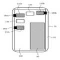
도 1 및 도 2는 예시적인 실시예들에 따른 화상 표시 장치를 나타내는 개략적인 단면도들이다.1 and 2 are schematic cross-sectional views showing an image display device according to exemplary embodiments.
도 1 및 도 2를 참조하면, 상기 화상 표시 장치는 인쇄 회로 기판(100) 및 디스플레이 패널(140)을 포함하며, 인쇄 회로 기판(PCB)(100) 상에 실장된 안테나(110a, 110b) 및 디스플레이 패널(140) 상에 배치된 전송 선로(170)를 포함할 수 있다.1 and 2, the image display apparatus includes a printed
인쇄 회로 기판(100)은 절연층들 및 내부 회로를 형성하는 금속층들이 반복 적층된 구조를 가질 수 있다. 인쇄 회로 기판(100) 상에는 상기 내부 회로와 전자 소자를 연결시키는 솔더(solder)와 같은 연결 패드들이 형성될 수 있다. 예를 들면, 인쇄 회로 기판(100)은 상기 화상 표시 장치의 메인 보드로 제공될 수 있다.The printed
인쇄 회로 기판(100) 상에는 예를 들면, 상기 연결 패드들을 통해 상기 전자 소자 및 안테나(110a, 110b)가 실장될 수 있다. 도 1에 도시된 바와 같이, 상기 전자 소자 및 안테나(110a, 110b)는 인쇄 회로 기판(100)의 상면 상에 배열될 수 있다. 도 2에 도시된 바와 같이, 상기 전자 소자 및 안테나(110a, 110b)는 인쇄 회로 기판(100)의 저면 상에 배열될 수도 있다.On the printed
일 실시예에 있어서, 상기 전자 소자 및 안테나(110a, 110b)는 인쇄 회로 기판(100)의 상기 상면 및 저면 상에 분산 배열될 수도 있다.In one embodiment, the electronic devices and
인쇄 회로 기판(100) 상에는 복수의 안테나들이 실장될 수 있다. 상기 복수의 안테나들은 서로 다른 공진 주파수를 가질 수 있다.A plurality of antennas may be mounted on the printed
예를 들면, 제1 안테나(110a) 및 제2 안테나(110b)가 인쇄 회로 기판(100) 상에 분리되어 실장될 수 있으며, 3개 이상의 안테나들이 실장될 수도 있다.For example, the
안테나들(110a, 110b)은 각각 방사 패턴을 포함하며, 전송 선로(170) 및/또는 인쇄 회로 기판(100)의 내부 회로와 연결을 위한 패드 전극을 포함할 수도 있다. 상기 방사 패턴 및 상기 패드 전극은 금속 또는 합금을 포함할 수 있다.The
안테나들(110a, 110b)은 각각 안테나 패치(patch) 또는 안테나 칩(chip) 형태로 인쇄 회로 기판(100) 상에 실장될 수 있다.The
상기 전자 소자는 예를 들면, 디스플레이 구동 집적 회로(IC) 칩(120), 메모리 소자(130) 등을 포함할 수 있다. 메모리 소자(130)는 예를 들면, 램(RAM) 소자 또는 플래시 메모리 소자 등을 포함할 수 있다.The electronic device may include, for example, a display drive integrated circuit (IC)
상기 전자 소자는 상기 화상 표시 장치에 포함되는 각종 센서 소자 들의 구동을 위한 IC 칩을 포함할 수도 있다. 예를 들면, 상기 전자 소자는 터치 센서 또는 터치 스크린 패널의 구동 IC 칩을 포함할 수도 있다.The electronic device may include an IC chip for driving various sensor elements included in the image display device. For example, the electronic device may include a touch sensor or a driving IC chip of a touch screen panel.
상기 전자 소자는 레지스터, 커패시터, 콘덴서 등과 같은 상기 화상 표시 장치의 각종 회로 구조물을 포함할 수도 있다.The electronic device may include various circuit structures of the image display device such as a resistor, a capacitor, a capacitor, and the like.
인쇄 회로 기판(100) 상에는 디스플레이 패널(140)이 배치될 수 있다. 예시적인 실시예들에 따르면, 인쇄 회로 기판(100) 및 디스플레이 패널(140)은 소정의 거리로 이격될 수 있다.A
예를 들면, 상기 화상 표시 장치의 하우징에 의해 인쇄 회로 기판(100) 및 디스플레이 패널(140)가 각각 고정되어, 인쇄 회로 기판(100) 및 디스플레이 패널(140) 사이에는 이격 공간이 형성될 수 있다.For example, the printed
일 실시예에 있어서, 상기 이격 공간 내에는 접착층, 스페이서 등과 같은 절연성 구조물이 배치될 수도 있다.In one embodiment, an insulating structure such as an adhesive layer, a spacer, or the like may be disposed in the spacing space.
디스플레이 패널(140)의 아래는 상기 화상 표시 장치의 배면부에 해당되며, 상술한 안테나(110a, 110b) 및 상기 전자 소자가 실장된 인쇄 회로 기판(100)이 배치될 수 있다. 디스플레이 패널(140)의 상측은 상기 화상 표시 장치의 이미지가 구현되는 전면부에 해당될 수 있다.The lower portion of the
디스플레이 패널(140)은 예를 들면, 박막 트랜지스터(TFT) 어레이 기판을 포함할 수 있다. 예를 들면, 상기 TFT 어레이 기판은 글래스 기판 혹은 수지 기판과 같은 베이스 기판, 상기 베이스 기판 상에 배열된 박막 트랜지스터, 스캔 라인, 데이터 라인 등을 포함할 수 있다. 도 1 및 도 2에서 참조부호 "140"은 디스플레이 패널 및 TFT 어레이 기판을 함께 지칭하기 위해 교호적으로 사용될 수 있다.The
디스플레이 패널(140)은 상기 TFT 어레이 기판 상에 배열된 화소 정의막(145) 및 표시층(150)을 포함할 수 있다. 예를 들면, 상기 박막 트랜지스터에 포함된 화소 전극이 화소 정의막(145)에 의해 부분적으로 노출되어 각 화소가 정의되며, 노출된 상기 화소 전극의 표면 상에 표시층(150)이 형성될 수 있다.The
화소 정의막(145)은 무기 절연 물질 또는 유기 절연 물질을 포함할 수 있다. 표시층(150)은 예를 들면, 유기 발광층 또는 액정층을 포함할 수 있다. 표시층(150)이 유기 발광층을 포함하는 경우, 상기 화상 표시 장치는 유기 발광 다이오드(OLED) 디스플레이 장치로 제공될 수 있다. 이 경우, 표시층(150)은 정공 수송층, 전자 수송층 등을 더 포함할 수도 있다.The
표시층(150)이 액정층을 포함하는 경우, 상기 화상 표시 장치는 액정 디스플레이(LCD) 장치로 제공될 수 있다. 이 경우, 디스플레이 패널(140) 및 인쇄 회로 기판(100) 사이에 백 라이트, 편광판 등이 더 배치될 수도 있다.When the
표시층(150) 상에는 반사 전극(155)이 배치될 수 있다. 예를 들면, 반사 전극(150)은 복수의 표시층들(150) 또는 화소들 상에서 연장되는 공통 전극으로 제공될 수도 있다.A
반사 전극(155) 및 화소 정의막(145) 상에는 유전층(160)이 형성될 수 있다. 유전층(160)은 디스플레이 패널(140)을 보호하는 하부 인캡슐레이션 층으로 기능할 수도 있다.A
유전층(160) 상에는 전송 선로(170)가 배치될 수 있다. 전송 선로(170)는 예를 들면, 안테나(110a, 110b)와 전기적으로 연결되어 안테나 구동 IC 칩과 안테나(110a, 110b) 사이의 급전 및 신호 송수신 경로로 제공될 수 있다.A
예시적인 실시예들에 따르면, 전송 선로(170)는 메쉬 구조를 포함할 수 있다. 예를 들면, 상기 방사 패턴에서 사용된 금속 또는 합금이 복수의 서로 교차하는 전극 라인 형태로 패터닝되어 전송 선로(170)가 형성될 수 있다. 이에 따라, 디스플레이 패널(140) 상측으로의 투과율이 향상되어 이미지 품질이 향상될 수 있다.According to exemplary embodiments, the
예시적인 실시예들에 따르면, 연결 구조물(180a, 180b)에 의해 디스플레이 패널(140) 상측 및 하측에 각각 위치한 전송 선로(170) 및 안테나(110a, 110b)가 서로 전기적으로 연결될 수 있다.The
일부 실시예들에 있어서, 제1 연결 구조물(180a)에 의해 전송 선로(170) 및 제1 안테나(110a)가 서로 연결될 수 있으며, 제2 연결 구조물(180b)에 의해 전송 선로(170) 및 제2 안테나(110b)가 서로 연결될 수 있다. 이에 따라, 전송 선로(170)를 통해 디스플레이 패널(140) 아래에 배치된 제1 및 제2 안테나들(110a, 110b)이 서로 전기적으로 연결 또는 그룹핑될 수 있다.The
연결 구조물(180a, 180b)은 금속 와이어 또는 연성 회로 기판(FPCB)을 포함할 수 있다.The
도 1에 도시된 바와 같이, 안테나(110a, 110b)가 인쇄 회로 기판(100)의 상면 상에 실장된 경우, 연결 구조물(180a, 180b)의 일단은 디스플레이 패널(140)위로 연장되어 전송 선로(170)의 일단부와 연결될 수 있다. 연결 구조물(180a, 180b)의 타단은 예를 들면, 디스플레이 패널(140) 및 인쇄 회로 기판(100) 사이로 절곡되어 안테나(110a, 110b)와 연결될 수 있다. 예를 들면, 연결 구조물(180a, 180b)의 타단은 안테나(110a, 110b)에 포함된 상기 패드 전극과 전기적으로 연결될 수 있다.1, when the
도 2에 도시된 바와 같이, 안테나(110a, 110b)가 인쇄 회로 기판(100)의 저면 상에 실장된 경우, 연결 구조물(180a, 180b)은 전송 선로(170)의 일단부로부터 인쇄 회로 기판(100)의 상기 저면까지 연장되어 안테나(110a, 110b)와 연결될 수 있다.2, when the
전송 선로(170) 상에는 상부 인캡슐레이션 층(190)이 형성될 수 있다. 상부 인캡슐레이션 층(190)은 실리콘 산화물, 실리콘 질화물과 같은 무기 절연 물질, 아크릴계 수지 또는 이미드계 수지 등과 같은 유기 절연 물질, 또는 유-무기 하이브리드 필름을 포함할 수 있다.An
상부 인캡슐레이션 층(190) 상에는 윈도우 기판(195)이 배치될 수 있다. 윈도우 기판(195)은 상기 화상 표시 장치의 사용자에게 시인면을 제공할 수 있다.A
일부 실시예들에 있어서, 상기 화상 표시 장치는 터치 센서 또는 터치 스크린 패널과 같은 센서 구조물 또는 편광판, 위상차 필름과 같은 광학 구조물등을 더 포함할 수 있다.In some embodiments, the image display device may further include a sensor structure such as a touch sensor or a touch screen panel or an optical structure such as a polarizing plate, a retardation film, and the like.
상기 센서 구조물 또는 광학 구조물은 윈도우 기판(195) 및 전송 선로(170) 사이에 배치될 수 있다. 이와는 달리, 상기 상기 센서 구조물 또는 광학 구조물은 전송 선로(170) 및 디스플레이 패널(140) 사이에 배치될 수 있다.The sensor structure or optical structure may be disposed between the
일 실시예에 있어서, 전송 선로(170)를 통한 신호 경로를 단축하고, 수신 감도를 향상 시키기 위해, 상기 센서 구조물 또는 광학 구조물은 윈도우 기판(195) 및 전송 선로(170) 사이에 배치될 수 있다.In one embodiment, the sensor structure or optical structure may be disposed between the
상술한 바와 같이, 예시적인 실시예들에 따르면 안테나(110a, 110b) 및 전송선로(170)을 디스플레이 패널(140)을 사이에 두고 서로 다른 레벨에 이격되도록 배치할 수 있다. 따라서, 디스플레이 구동 집적 회로(IC) 칩(120), 메모리 소자(130)와 같은 전자 소자에 의한 공간 제약에 무관하게 전송 선로(170)를 배열할 수 있으며, 이에 따라 신호 경로를 단축시켜 전송 선로(170)를 통한 저항 증가 또는 신호 손실을 방지할 수 있다.As described above, according to the exemplary embodiments, the
도 3은 일부 실시예들에 있어서, 전송 선로 주변의 더미 패턴을 도시한 개략적인 평면도이다.3 is a schematic plan view showing a dummy pattern around a transmission line, in some embodiments.
도 3을 참조하면, 도 1 및 도 2를 참조로 설명한 바와 같이, 유전층(160) 상에 전송 선로(170)가 배치되며, 전송 선로(170)는 메쉬 구조를 포함할 수 있다.Referring to FIG. 3, a
예시적인 실시예들에 따르면, 유전층(160) 상에서 전송 선로(170) 주변에 더미 패턴(172)을 포함할 수 있다. 더미 패턴(172)은 전송 선로(170)와 소정의 거리로 이격되어 전송 선로(170)와 전기적, 물리적으로 분리될 수 있다.According to exemplary embodiments, a
더미 패턴(172)은 전송 선로(170)와 실질적으로 동일하거나 유사한 메쉬 구조를 포함할 수 있다.The
예를 들면, 더미 패턴(172)은 전송 선로(170)와 동일한 물질로 형성되며, 전극 라인의 선폭 및 개구율이 전송 선로(170)와 동일한 메쉬 구조를 포함할 수 있다. 따라서, 전송 선로(170)에 의한 광학적 편차가 감소되어, 전송 선로(170)가 화상 표시 장치의 사용자에게 시인되는 것을 방지할 수 있다.For example, the
도 4 및 도 5는 예시적인 실시예들에 따른 화상 표시 장치를 나타내는 개략적인 평면도들이다. 예를 들면, 도 4는 화상 표시 장치의 전면부를 나타내는 평면도이며, 도 5는 화상 표시 장치의 배면 커버가 제거된 배면부를 나타내는 평면도이다.Figs. 4 and 5 are schematic plan views showing an image display device according to exemplary embodiments. Fig. For example, Fig. 4 is a plan view showing the front portion of the image display apparatus, and Fig. 5 is a plan view showing the back portion of the image display apparatus from which the rear cover is removed.
도 4 및 도 5를 참조하면, 상기 화상 표시 장치는 상기 전면부에 표시 영역(50) 및 주변 영역(60)을 포함할 수 있다. 표시 영역(50)을 통해 도 1 또는 도 2에 도시된 디스플레이 패널(140)로부터 생성된 이미지가 사용자에게 표시될 수 있다. 디스플레이 패널(140) 상에는 전송 선로(170)가 배치되며, 전송 선로(170)는 실질적으로 투명한 메쉬 구조를 포함하므로, 이미지 품질의 저하를 방지할 수 있다.4 and 5, the image display apparatus may include a
주변 영역(60)은 표시 영역(50)의 양 단부 및 양 측부에 배치된 영역일 수 있다. 주변 영역(60)은 상기 화상 표시 장치의 하우징(70) 및 인쇄 회로 기판(100)사이의 베젤 영역(65)을 포함할 수 있다.The
인쇄 회로 기판(100) 상에는 안테나들(110a, 110b, 110c)이 실장되며, 전자 소자들(120, 130)이 함께 실장될 수 있다. 또한, 인쇄 회로 기판(100) 상에는 배터리(80)가 결합될 수 있다.The
도 1 및 도 2를 참조로 설명한 바와 같이, 연성 회로 기판(FPCB)과 같은 연결 구조물(180a, 180b, 180c)이 각각 디스플레이 패널(140) 상의 전송 선로(170)와 연결되고, 인쇄회로 기판(100) 쪽으로 연장되어 베젤 영역(65)을 통해 안테나들(110a, 110b, 110c)과 연결될 수 있다. 이에 따라, 안테나들(110a, 110b, 110c)은 전송 선로(170)를 통해 서로 전기적으로 연결되어 예를 들면, 안테나 구동 IC 칩을 통해 함께 제어 및 급전될 수 있다.1 and 2, connecting
또한, 연결 구조물(180a, 180b, 180c)은 베젤 영역(65)을 통해 안테나들(110a, 110b, 110c)과 연결되므로, 표시 영역(50)에서의 이미지 구현을 저해하지 않을 수 있다.Since the
도 6은 비교예에 따른 화상 표시 장치를 나타내는 개략적인 평면도이다.6 is a schematic plan view showing an image display apparatus according to a comparative example.
도 6을 참조하면, 비교예에 있어서 제1 내지 제3 안테나들(110a, 110b, 110c)이 전자 소자들(120, 130)과 함께 인쇄 회로 기판(100) 상에 실장되며, 전송 선로들(90) 역시 안테나들(110a, 110b, 110c)과 함께 인쇄 회로 기판(100) 상에 실장된다.6, the first to
제1 안테나(110a) 및 제2 안테나(110b)를 서로 연결시키기 위한 전송선로(90)는 디스플레이 구동 집적 회로(IC) 칩(120)을 우회하여 배치되고, 제2 안테나(110b) 및 제3 안테나(110c)를 서로 연결시키기 위한 전송선로(90)는 메모리 소자(130)를 우회하여 배치된다.The
따라서, 전송 선로(90)의 길이가 증가되며, 저항 증가로 인한 신호 손실 레벨이 증대될 수 있다. 또한, 인쇄 회로 기판(100)에 내장되거나, 연결된 레지스터, 콘덴서, 커패시터 등에 의한 RLC 노이즈에 의해 안테나 신호가 간섭 또는 교란될 수 있다.Therefore, the length of the
그러나, 도 1 내지 도 5를 참조로 설명한 예시적인 실시예들에 따르면, 전송 선로(170)를 디스플레이 패널(140)을 사이에 두고 안테나(110a, 110b, 110c)와 이격시키고, 베젤 영역(65)을 통해 연결 구조물(180a, 180b, 180c)로 안테나(110a, 110b, 110c) 및 전송선로(170)를 서로 연결시킬 수 있다.However, according to the exemplary embodiments described with reference to Figs. 1 to 5, the
따라서, 인쇄 회로 기판(100) 상에 실장된 각종 전자 소자 및 회로 소자에 의한 노이즈로부터 실질적으로 자유로우며, 신호 경로가 단축된 안테나 구동이 구현될 수 있다.Therefore, antenna driving which is substantially free from noise due to various electronic elements and circuit elements mounted on the printed
도 7 및 도 8은 예시적인 실시예들에 따른 전송 선로 구조를 나타내는 개략적인 단면도들이다.7 and 8 are schematic cross-sectional views illustrating a transmission line structure according to exemplary embodiments.
도 7을 참조하면, 상술한 바와 같이 전송 선로(170)는 디스플레이 패널(140) 상에 형성된 유전층(160) 상에 배열될 수 있다.Referring to FIG. 7, the
유전층(160)은 소정의 유전율을 갖는 절연 물질을 포함할 수 있다. 유전층(160)은 예를 들면, 실리콘 산화물, 실리콘 질화물, 금속 산화물 등과 같은 무기 절연 물질, 또는 에폭시 수지, 아크릴 수지, 이미드 계열 수지, 스티렌계 수지, 폴리에스테르계 수지, 우레탄계 수지 등과 같은 유기 절연 물질을 포함할 수 있다.The
일부 실시예들에 있어서, 유전층(160)의 유전율은 약 1.5 내지 12 범위로 조절될 수 있다. 상기 유전율이 약 12를 초과하는 경우, 구동 주파수가 지나치게 감소하여, 원하는 고주파 대역에서의 구동이 구현되지 않을 수 있다.In some embodiments, the dielectric constant of the
전송 선로(170)는 신호 라인(171) 및 그라운드 라인(173a, 173b)을 포함할 수 있다. 일부 실시예들에 있어서, 신호 라인(171)은 한 쌍의 그라운드 라인들(173a, 173b) 사이에 배치될 수 있다.The
이 경우, 신호 라인(171)은 연결 구조물(180a, 180b, 180c)을 통해 안테나(110a, 110b, 110c)와 전기적으로 연결될 수 있다. 그라운드 라인(173a, 173b)은 연결 구조물(180a, 180b, 180c)에 포함된 그라운드 배선 또는 그라운드 패턴과 연결될 수 있다.In this case, the
도 8을 참조하면, 유전층(160)의 상면 상에 전송선로(170)가 배치되며, 전송 선로(170)의 저면 상에 그라운드 층(165)이 형성될 수 있다.Referring to FIG. 8, a
일부 실시예들에 있어서, 디스플레이 패널(140)에 포함된 도전성 부재가 그라운드 층(165)으로 제공될 수 있다. 상기 도전성 부재는 예를 들면, 디스플레이 패널(140)에 포함된 박막 트랜지스터(TFT)의 게이트 전극, 스캔 라인 또는 데이터 라인과 같은 각종 배선, 또는 화소 전극, 공통 전극과 같은 각종 전극 등을 포함할 수 있다.In some embodiments, a conductive member included in the
일 실시예에 있어서, 디스플레이 패널(140)에 포함된 반사 전극(155)이 그라운드 층(165)으로 제공될 수도 있다.In one embodiment, the
50: 표시 영역60: 주변 영역
65: 베젤 영역70: 하우징
100: 인쇄 회로 기판110a, 110b, 110c: 안테나
120: 디스플레이 구동 IC 칩130: 메모리 소자
140: 디스플레이 패널145: 화소 정의막
150: 표시층160: 유전층
170: 전송 선로180a, 180b, 180c: 연결 구조물
190: 상부 인캡슐레이션 층195: 윈도우 기판50: display area 60: peripheral area
65: Bezel area 70: Housing
100: printed
120: display driving IC chip 130: memory element
140: Display panel 145: Pixel definition film
150: display layer 160: dielectric layer
170:
190: upper encapsulation layer 195: window substrate
Claims (16)
Translated fromKorean상기 인쇄 회로 기판 상에 실장된 안테나;
상기 인쇄 회로 기판 위로 배치되는 디스플레이 패널; 및
상기 디스플레이 패널 상에 배치되며 상기 안테나와 전기적으로 연결되는 전송 선로를 포함하며
상기 안테나와 전송 선로는 상기 디스플레이 패널을 사이에 두고 다른 층에 이격 되어 배치된, 화상 표시 장치.
Printed circuit board;
An antenna mounted on the printed circuit board;
A display panel disposed over the printed circuit board; And
And a transmission line disposed on the display panel and electrically connected to the antenna,
Wherein the antenna and the transmission line are disposed apart from each other with the display panel interposed therebetween.
The image display apparatus according to claim 1, further comprising an electronic element mounted on the printed circuit board.
The image display device according to claim 2, wherein the electronic device includes a display driving integrated circuit (IC) chip and a memory device.
The image display apparatus according to claim 2, wherein the electronic element and the antenna are mounted on the same surface of the printed circuit board.
The image display device according to claim 1, further comprising a connection structure for electrically connecting the transmission line and the antenna to each other.
The image display apparatus according to claim 5, wherein the connection structure includes a flexible printed circuit board (FPCB).
The image display apparatus according to claim 5, wherein the connection structure is connected to one end of the transmission line and extends toward the printed circuit board through a peripheral region of the image display device, and is connected to the antenna.
The image display apparatus according to claim 5, wherein a plurality of the antennas are electrically connected to each other through the plurality of connection structures and the transmission line.
The image display apparatus according to claim 1, wherein the transmission line includes a mesh structure.
The image display apparatus according to claim 9, further comprising a dummy pattern arranged around the transmission line and including the same mesh structure as the mesh structure of the transmission line.
The image display apparatus according to claim 1, further comprising a dielectric layer disposed on the display panel, wherein the transmission line is arranged on an upper surface of the dielectric layer.
한 쌍의 그라운드 라인들; 및
상기 그라운드 라인들 사이에 배치된 신호 라인을 포함하는, 화상 표시 장치.
[12] The method of claim 11,
A pair of ground lines; And
And a signal line disposed between the ground lines.
12. The image display apparatus according to claim 11, further comprising a ground layer disposed on a bottom surface of the dielectric layer.
14. The image display apparatus according to claim 13, wherein the display panel includes a thin film transistor array substrate, a display layer and an electrode, and the electrode of the display panel is provided as the ground layer.
상기 전송 선로 상에 배치된 상부 인캡슐레이션 층; 및
상기 상부 인캡슐레이션 층 상에 배치된 윈도우 기판을 더 포함하는, 화상 표시 장치.
The method according to claim 1,
An upper encapsulation layer disposed on the transmission line; And
And a window substrate disposed on the upper encapsulation layer.
상기 유전층 상에 배치된 전송 선로;
상기 유전층 아래에 배치되며, 디스플레이 패널을 사이에 두고 상기 유전층과 이격된 방사 패턴; 및
상기 방사 패턴 및 상기 전송 선로를 서로 전기적으로 연결시키는 연결 구조물을 포함하며
상기 방사 패턴과 상기 전송 선로는 상기 디스플레이 패널을 사이에 두고 다른 층에 이격되어 배치된, 화상 표시 장치용 안테나.Dielectric layer;
A transmission line disposed on the dielectric layer;
A radiation pattern disposed below the dielectric layer and spaced apart from the dielectric layer with a display panel therebetween; And
And a connection structure for electrically connecting the radiation pattern and the transmission line to each other
Wherein the radiation pattern and the transmission line are disposed apart from each other with the display panel interposed therebetween.
Priority Applications (4)
| Application Number | Priority Date | Filing Date | Title |
|---|---|---|---|
| KR1020180026380AKR101962819B1 (en) | 2018-03-06 | 2018-03-06 | Image display device intgrated with antenna and antenna for image display device |
| CN201980016950.4ACN111801845B (en) | 2018-03-06 | 2019-03-06 | Image display device integrated with antenna and antenna for image display device |
| PCT/KR2019/002565WO2019172630A1 (en) | 2018-03-06 | 2019-03-06 | Image display device integrated with antenna and antenna for image display device |
| US17/012,505US12100887B2 (en) | 2018-03-06 | 2020-09-04 | Image display device integrated with antenna and antenna for image display device |
Applications Claiming Priority (1)
| Application Number | Priority Date | Filing Date | Title |
|---|---|---|---|
| KR1020180026380AKR101962819B1 (en) | 2018-03-06 | 2018-03-06 | Image display device intgrated with antenna and antenna for image display device |
Publications (1)
| Publication Number | Publication Date |
|---|---|
| KR101962819B1true KR101962819B1 (en) | 2019-03-27 |
Family
ID=65906831
Family Applications (1)
| Application Number | Title | Priority Date | Filing Date |
|---|---|---|---|
| KR1020180026380AActiveKR101962819B1 (en) | 2018-03-06 | 2018-03-06 | Image display device intgrated with antenna and antenna for image display device |
Country Status (4)
| Country | Link |
|---|---|
| US (1) | US12100887B2 (en) |
| KR (1) | KR101962819B1 (en) |
| CN (1) | CN111801845B (en) |
| WO (1) | WO2019172630A1 (en) |
Cited By (7)
| Publication number | Priority date | Publication date | Assignee | Title |
|---|---|---|---|---|
| WO2021033806A1 (en)* | 2019-08-22 | 2021-02-25 | 엘지전자 주식회사 | Electronic device equipped with transparent antenna |
| WO2021033805A1 (en)* | 2019-08-22 | 2021-02-25 | 엘지전자 주식회사 | Electronic device having transparent antenna |
| CN113360018A (en)* | 2020-03-05 | 2021-09-07 | 东友精细化工有限公司 | Antenna package and image display device including the same |
| CN113540168A (en)* | 2020-04-13 | 2021-10-22 | 东友精细化工有限公司 | Antenna integrated display panel |
| WO2021221346A1 (en)* | 2020-04-29 | 2021-11-04 | 동우화인켐 주식회사 | Antenna laminate and display device comprising same |
| CN114498010A (en)* | 2020-11-13 | 2022-05-13 | 东友精细化工有限公司 | Antenna elements and display devices |
| US11538889B2 (en) | 2019-10-31 | 2022-12-27 | Samsung Display Co., Ltd. | Display apparatus and electronic apparatus including the same |
Families Citing this family (1)
| Publication number | Priority date | Publication date | Assignee | Title |
|---|---|---|---|---|
| CN113036418B (en)* | 2021-03-23 | 2023-02-21 | 维沃移动通信有限公司 | Display panels and electronics |
Citations (5)
| Publication number | Priority date | Publication date | Assignee | Title |
|---|---|---|---|---|
| JP4300873B2 (en)* | 2003-05-13 | 2009-07-22 | パナソニック株式会社 | Electromagnetic shield mechanism |
| KR20130070247A (en)* | 2011-12-19 | 2013-06-27 | 엘지전자 주식회사 | Touch panel and mobile/portable terminal including the same |
| KR20160059291A (en) | 2014-11-18 | 2016-05-26 | 주식회사 에이치시티엠 | Antenna positioned to display adhesive layer and manufacturing method thereof |
| KR20170073772A (en)* | 2015-12-18 | 2017-06-29 | 엘지디스플레이 주식회사 | Optical Wave-Guiding Film And Organic Light Emitting Diode Display Device Including The Same |
| JP2017175540A (en)* | 2016-03-25 | 2017-09-28 | 大日本印刷株式会社 | antenna |
Family Cites Families (17)
| Publication number | Priority date | Publication date | Assignee | Title |
|---|---|---|---|---|
| CN101098044A (en)* | 2006-06-30 | 2008-01-02 | 佛山市顺德区顺达电脑厂有限公司 | Antenna arrangement and configuration mode |
| KR20080028679A (en)* | 2006-09-27 | 2008-04-01 | 삼성전자주식회사 | Printed circuit board and display device having same |
| KR20110071368A (en)* | 2009-12-21 | 2011-06-29 | (주)파트론 | Diversity Antenna Using Broadband Patch Antenna |
| US20140106684A1 (en)* | 2012-10-15 | 2014-04-17 | Qualcomm Mems Technologies, Inc. | Transparent antennas on a display device |
| KR102168132B1 (en)* | 2013-12-31 | 2020-10-21 | 삼성디스플레이 주식회사 | Organic light emitting device |
| KR20160080444A (en)* | 2014-12-29 | 2016-07-08 | 삼성전자주식회사 | Antenna device and electronic device with the same |
| KR102275318B1 (en)* | 2015-03-02 | 2021-07-13 | 삼성디스플레이 주식회사 | Image display apparatus |
| KR102399741B1 (en)* | 2015-05-22 | 2022-05-20 | 삼성전자주식회사 | Display module and method of manufacturing the same |
| KR102567364B1 (en)* | 2016-01-27 | 2023-08-16 | 삼성전자주식회사 | Antenna Assist Device and Electronic device including the same |
| KR102499120B1 (en)* | 2016-02-17 | 2023-02-15 | 삼성전자주식회사 | Electronic device including antenna |
| KR102466002B1 (en)* | 2016-04-19 | 2022-11-11 | 삼성전자주식회사 | Electronic device including antenna |
| KR102334098B1 (en) | 2016-04-20 | 2021-12-03 | 삼성전자주식회사 | Electronic device including display |
| KR102158304B1 (en)* | 2018-08-30 | 2020-09-22 | 동우 화인켐 주식회사 | High frequency film transmission line, antenna including the same and antenna-integrated image display device |
| KR20220053865A (en)* | 2020-10-23 | 2022-05-02 | 동우 화인켐 주식회사 | Antenna package and image display device including the same |
| KR102755830B1 (en)* | 2020-11-17 | 2025-01-20 | 동우 화인켐 주식회사 | Antenna package and image display device including the same |
| KR20220083150A (en)* | 2020-12-11 | 2022-06-20 | 동우 화인켐 주식회사 | Antenna package and image display device including the same |
| KR102390288B1 (en)* | 2021-07-05 | 2022-04-22 | 동우 화인켐 주식회사 | Antenna structure and image display device including the same |
- 2018
- 2018-03-06KRKR1020180026380Apatent/KR101962819B1/enactiveActive
- 2019
- 2019-03-06WOPCT/KR2019/002565patent/WO2019172630A1/ennot_activeCeased
- 2019-03-06CNCN201980016950.4Apatent/CN111801845B/enactiveActive
- 2020
- 2020-09-04USUS17/012,505patent/US12100887B2/enactiveActive
Patent Citations (5)
| Publication number | Priority date | Publication date | Assignee | Title |
|---|---|---|---|---|
| JP4300873B2 (en)* | 2003-05-13 | 2009-07-22 | パナソニック株式会社 | Electromagnetic shield mechanism |
| KR20130070247A (en)* | 2011-12-19 | 2013-06-27 | 엘지전자 주식회사 | Touch panel and mobile/portable terminal including the same |
| KR20160059291A (en) | 2014-11-18 | 2016-05-26 | 주식회사 에이치시티엠 | Antenna positioned to display adhesive layer and manufacturing method thereof |
| KR20170073772A (en)* | 2015-12-18 | 2017-06-29 | 엘지디스플레이 주식회사 | Optical Wave-Guiding Film And Organic Light Emitting Diode Display Device Including The Same |
| JP2017175540A (en)* | 2016-03-25 | 2017-09-28 | 大日本印刷株式会社 | antenna |
Cited By (17)
| Publication number | Priority date | Publication date | Assignee | Title |
|---|---|---|---|---|
| WO2021033805A1 (en)* | 2019-08-22 | 2021-02-25 | 엘지전자 주식회사 | Electronic device having transparent antenna |
| WO2021033806A1 (en)* | 2019-08-22 | 2021-02-25 | 엘지전자 주식회사 | Electronic device equipped with transparent antenna |
| US12009585B2 (en) | 2019-08-22 | 2024-06-11 | Lg Electronics Inc. | Electronic device equipped with transparent antenna |
| US11538889B2 (en) | 2019-10-31 | 2022-12-27 | Samsung Display Co., Ltd. | Display apparatus and electronic apparatus including the same |
| US11903282B2 (en) | 2019-10-31 | 2024-02-13 | Samsung Display Co., Ltd. | Display apparatus and electronic apparatus including the same |
| KR102703342B1 (en)* | 2020-03-05 | 2024-09-04 | 동우 화인켐 주식회사 | Antenna package and image display device including the same |
| KR20210112600A (en)* | 2020-03-05 | 2021-09-15 | 동우 화인켐 주식회사 | Antenna package and image display device including the same |
| WO2021177717A1 (en)* | 2020-03-05 | 2021-09-10 | 동우화인켐 주식회사 | Antenna package and image display device comprising same |
| CN113360018A (en)* | 2020-03-05 | 2021-09-07 | 东友精细化工有限公司 | Antenna package and image display device including the same |
| US12244054B2 (en) | 2020-03-05 | 2025-03-04 | Dongwoo Fine-Chem Co., Ltd. | Antenna package and image display device including the same |
| CN113540168A (en)* | 2020-04-13 | 2021-10-22 | 东友精细化工有限公司 | Antenna integrated display panel |
| WO2021221346A1 (en)* | 2020-04-29 | 2021-11-04 | 동우화인켐 주식회사 | Antenna laminate and display device comprising same |
| US12374779B2 (en) | 2020-04-29 | 2025-07-29 | Dongwoo Fine-Chem Co., Ltd. | Antenna laminate and display device including the same |
| CN114498010A (en)* | 2020-11-13 | 2022-05-13 | 东友精细化工有限公司 | Antenna elements and display devices |
| KR20220065474A (en)* | 2020-11-13 | 2022-05-20 | 동우 화인켐 주식회사 | Antenna device and display device including the same |
| CN114498010B (en)* | 2020-11-13 | 2025-06-06 | 东友精细化工有限公司 | Antenna element and display device |
| KR102839227B1 (en)* | 2020-11-13 | 2025-07-25 | 동우 화인켐 주식회사 | Antenna device and display device including the same |
Also Published As
| Publication number | Publication date |
|---|---|
| CN111801845A (en) | 2020-10-20 |
| WO2019172630A1 (en) | 2019-09-12 |
| US20200403297A1 (en) | 2020-12-24 |
| CN111801845B (en) | 2024-01-30 |
| US12100887B2 (en) | 2024-09-24 |
Similar Documents
| Publication | Publication Date | Title |
|---|---|---|
| KR101962819B1 (en) | Image display device intgrated with antenna and antenna for image display device | |
| CN110875523B (en) | Film transmission line, antenna and image display device | |
| KR101940798B1 (en) | Film antenna and display device including the same | |
| KR102099830B1 (en) | Antenna-combined module and display device including the same | |
| US9728840B2 (en) | Display panel and manufacturing method thereof, display device | |
| KR100707105B1 (en) | Ic tag mounted liquid crystal indicator and the manufacturing method | |
| KR20200038797A (en) | Touch sensor-antenna module and display device including the same | |
| US20210203056A1 (en) | High frequency film transmission line, antenna comprising same, and image display device having antenna coupled thereto | |
| KR20190021837A (en) | Film antenna and display device including the same | |
| KR102680193B1 (en) | Antenna device and display device including the same | |
| KR102150998B1 (en) | Antenna-combined module and display device including the same | |
| US20220140495A1 (en) | Antenna element, antenna array and display device including the same | |
| KR102541132B1 (en) | Antrnna array, antrnna device and display device including the same | |
| KR20230144796A (en) | Antenna structure and display device including the same | |
| KR102448037B1 (en) | Antenna coupling module and display device including same | |
| KR102703342B1 (en) | Antenna package and image display device including the same | |
| KR102789622B1 (en) | Antenna device and image display device including the same | |
| CN119730596A (en) | Display device | |
| KR102785352B1 (en) | High frequency film transmission line, antenna including the same and antenna-integrated image display device | |
| KR102243537B1 (en) | High frequency film transmission line, antenna including the same and antenna-integrated image display device | |
| KR102702866B1 (en) | Antenna device and display device including the same | |
| US20240055751A1 (en) | Display device | |
| CN115483261B (en) | Display panel, display module and display device | |
| CN120636258A (en) | Display module and display device |
Legal Events
| Date | Code | Title | Description |
|---|---|---|---|
| PA0109 | Patent application | Patent event code:PA01091R01D Comment text:Patent Application Patent event date:20180306 | |
| PA0201 | Request for examination | Patent event code:PA02012R01D Patent event date:20180814 Comment text:Request for Examination of Application Patent event code:PA02011R01I Patent event date:20180306 Comment text:Patent Application | |
| PA0302 | Request for accelerated examination | Patent event date:20180814 Patent event code:PA03022R01D Comment text:Request for Accelerated Examination Patent event date:20180306 Patent event code:PA03021R01I Comment text:Patent Application | |
| PE0902 | Notice of grounds for rejection | Comment text:Notification of reason for refusal Patent event date:20181001 Patent event code:PE09021S01D | |
| E701 | Decision to grant or registration of patent right | ||
| PE0701 | Decision of registration | Patent event code:PE07011S01D Comment text:Decision to Grant Registration Patent event date:20190306 | |
| GRNT | Written decision to grant | ||
| PR0701 | Registration of establishment | Comment text:Registration of Establishment Patent event date:20190321 Patent event code:PR07011E01D | |
| PR1002 | Payment of registration fee | Payment date:20190321 End annual number:3 Start annual number:1 | |
| PG1601 | Publication of registration | ||
| PR1001 | Payment of annual fee | Payment date:20211206 Start annual number:4 End annual number:4 | |
| PR1001 | Payment of annual fee | Payment date:20221207 Start annual number:5 End annual number:5 |