KR101960709B1 - Apparatus for organic layer deposition, method for manufacturing of organic light emitting display apparatus using the same, and organic light emitting display apparatus manufactured by the method - Google Patents
Apparatus for organic layer deposition, method for manufacturing of organic light emitting display apparatus using the same, and organic light emitting display apparatus manufactured by the methodDownload PDFInfo
- Publication number
- KR101960709B1 KR101960709B1KR1020120076940AKR20120076940AKR101960709B1KR 101960709 B1KR101960709 B1KR 101960709B1KR 1020120076940 AKR1020120076940 AKR 1020120076940AKR 20120076940 AKR20120076940 AKR 20120076940AKR 101960709 B1KR101960709 B1KR 101960709B1
- Authority
- KR
- South Korea
- Prior art keywords
- substrate
- deposition
- correction
- unit
- layer deposition
- Prior art date
- Legal status (The legal status is an assumption and is not a legal conclusion. Google has not performed a legal analysis and makes no representation as to the accuracy of the status listed.)
- Active
Links
- 230000008021depositionEffects0.000titleclaimsabstractdescription303
- 239000012044organic layerSubstances0.000titleclaimsabstractdescription160
- 238000000034methodMethods0.000titleclaimsabstractdescription46
- 238000004519manufacturing processMethods0.000titleclaimsabstractdescription19
- 238000012937correctionMethods0.000claimsabstractdescription114
- 238000000151depositionMethods0.000claimsdescription315
- 238000001704evaporationMethods0.000claimsdescription247
- 230000008020evaporationEffects0.000claimsdescription245
- 239000000758substrateSubstances0.000claimsdescription193
- 239000010410layerSubstances0.000claimsdescription139
- 239000000463materialSubstances0.000claimsdescription98
- 238000012546transferMethods0.000claimsdescription64
- 238000000429assemblyMethods0.000claimsdescription59
- 230000000712assemblyEffects0.000claimsdescription59
- 230000000903blocking effectEffects0.000claimsdescription55
- 238000007740vapor depositionMethods0.000claimsdescription8
- 238000000059patterningMethods0.000description112
- 238000005339levitationMethods0.000description18
- 239000010408filmSubstances0.000description12
- 230000000694effectsEffects0.000description9
- 239000011368organic materialSubstances0.000description7
- 230000008569processEffects0.000description7
- 238000000427thin-film depositionMethods0.000description7
- 238000005530etchingMethods0.000description6
- 239000004065semiconductorSubstances0.000description6
- 229910001111Fine metalInorganic materials0.000description5
- 229910052782aluminiumInorganic materials0.000description5
- 238000002347injectionMethods0.000description5
- 239000007924injectionSubstances0.000description5
- 238000005259measurementMethods0.000description5
- 239000011229interlayerSubstances0.000description4
- 230000004048modificationEffects0.000description4
- 238000012986modificationMethods0.000description4
- 238000005137deposition processMethods0.000description3
- 239000002019doping agentSubstances0.000description3
- 239000011521glassSubstances0.000description3
- 238000010438heat treatmentMethods0.000description3
- 239000011159matrix materialSubstances0.000description3
- 239000010409thin filmSubstances0.000description3
- XEEYBQQBJWHFJM-UHFFFAOYSA-NIronChemical compound[Fe]XEEYBQQBJWHFJM-UHFFFAOYSA-N0.000description2
- 150000001875compoundsChemical class0.000description2
- 230000007547defectEffects0.000description2
- 230000002950deficientEffects0.000description2
- 238000005516engineering processMethods0.000description2
- 230000004907fluxEffects0.000description2
- 230000005525hole transportEffects0.000description2
- 229910052749magnesiumInorganic materials0.000description2
- 238000002161passivationMethods0.000description2
- 239000011241protective layerSubstances0.000description2
- 229910052709silverInorganic materials0.000description2
- 229910052779NeodymiumInorganic materials0.000description1
- 230000004888barrier functionEffects0.000description1
- 239000003990capacitorSubstances0.000description1
- 229910052804chromiumInorganic materials0.000description1
- 238000004140cleaningMethods0.000description1
- 239000002131composite materialSubstances0.000description1
- XCJYREBRNVKWGJ-UHFFFAOYSA-Ncopper(II) phthalocyanineChemical compound[Cu+2].C12=CC=CC=C2C(N=C2[N-]C(C3=CC=CC=C32)=N2)=NC1=NC([C]1C=CC=CC1=1)=NC=1N=C1[C]3C=CC=CC3=C2[N-]1XCJYREBRNVKWGJ-UHFFFAOYSA-N0.000description1
- 238000009795derivationMethods0.000description1
- 238000001312dry etchingMethods0.000description1
- 229910052737goldInorganic materials0.000description1
- 230000005484gravityEffects0.000description1
- RBTKNAXYKSUFRK-UHFFFAOYSA-Nheliogen blueChemical compound[Cu].[N-]1C2=C(C=CC=C3)C3=C1N=C([N-]1)C3=CC=CC=C3C1=NC([N-]1)=C(C=CC=C3)C3=C1N=C([N-]1)C3=CC=CC=C3C1=N2RBTKNAXYKSUFRK-UHFFFAOYSA-N0.000description1
- PJXISJQVUVHSOJ-UHFFFAOYSA-Nindium(III) oxideInorganic materials[O-2].[O-2].[O-2].[In+3].[In+3]PJXISJQVUVHSOJ-UHFFFAOYSA-N0.000description1
- 238000007689inspectionMethods0.000description1
- 229910052741iridiumInorganic materials0.000description1
- 229910052742ironInorganic materials0.000description1
- 239000000696magnetic materialSubstances0.000description1
- 239000007769metal materialSubstances0.000description1
- IBHBKWKFFTZAHE-UHFFFAOYSA-Nn-[4-[4-(n-naphthalen-1-ylanilino)phenyl]phenyl]-n-phenylnaphthalen-1-amineChemical compoundC1=CC=CC=C1N(C=1C2=CC=CC=C2C=CC=1)C1=CC=C(C=2C=CC(=CC=2)N(C=2C=CC=CC=2)C=2C3=CC=CC=C3C=CC=2)C=C1IBHBKWKFFTZAHE-UHFFFAOYSA-N0.000description1
- 229910052759nickelInorganic materials0.000description1
- 239000005416organic matterSubstances0.000description1
- 229910052763palladiumInorganic materials0.000description1
- 238000005192partitionMethods0.000description1
- 238000000206photolithographyMethods0.000description1
- IEQIEDJGQAUEQZ-UHFFFAOYSA-NphthalocyanineChemical compoundN1C(N=C2C3=CC=CC=C3C(N=C3C4=CC=CC=C4C(=N4)N3)=N2)=C(C=CC=C2)C2=C1N=C1C2=CC=CC=C2C4=N1IEQIEDJGQAUEQZ-UHFFFAOYSA-N0.000description1
- 229910052697platinumInorganic materials0.000description1
- 239000003507refrigerantSubstances0.000description1
- 230000004044responseEffects0.000description1
- 125000006850spacer groupChemical group0.000description1
- 238000004544sputter depositionMethods0.000description1
- 239000000126substanceSubstances0.000description1
- 239000012780transparent materialSubstances0.000description1
- TVIVIEFSHFOWTE-UHFFFAOYSA-Ktri(quinolin-8-yloxy)alumaneChemical compound[Al+3].C1=CN=C2C([O-])=CC=CC2=C1.C1=CN=C2C([O-])=CC=CC2=C1.C1=CN=C2C([O-])=CC=CC2=C1TVIVIEFSHFOWTE-UHFFFAOYSA-K0.000description1
- 230000000007visual effectEffects0.000description1
- 238000003466weldingMethods0.000description1
Images


Classifications
- C—CHEMISTRY; METALLURGY
- C23—COATING METALLIC MATERIAL; COATING MATERIAL WITH METALLIC MATERIAL; CHEMICAL SURFACE TREATMENT; DIFFUSION TREATMENT OF METALLIC MATERIAL; COATING BY VACUUM EVAPORATION, BY SPUTTERING, BY ION IMPLANTATION OR BY CHEMICAL VAPOUR DEPOSITION, IN GENERAL; INHIBITING CORROSION OF METALLIC MATERIAL OR INCRUSTATION IN GENERAL
- C23C—COATING METALLIC MATERIAL; COATING MATERIAL WITH METALLIC MATERIAL; SURFACE TREATMENT OF METALLIC MATERIAL BY DIFFUSION INTO THE SURFACE, BY CHEMICAL CONVERSION OR SUBSTITUTION; COATING BY VACUUM EVAPORATION, BY SPUTTERING, BY ION IMPLANTATION OR BY CHEMICAL VAPOUR DEPOSITION, IN GENERAL
- C23C14/00—Coating by vacuum evaporation, by sputtering or by ion implantation of the coating forming material
- C23C14/22—Coating by vacuum evaporation, by sputtering or by ion implantation of the coating forming material characterised by the process of coating
- C23C14/24—Vacuum evaporation
- C—CHEMISTRY; METALLURGY
- C23—COATING METALLIC MATERIAL; COATING MATERIAL WITH METALLIC MATERIAL; CHEMICAL SURFACE TREATMENT; DIFFUSION TREATMENT OF METALLIC MATERIAL; COATING BY VACUUM EVAPORATION, BY SPUTTERING, BY ION IMPLANTATION OR BY CHEMICAL VAPOUR DEPOSITION, IN GENERAL; INHIBITING CORROSION OF METALLIC MATERIAL OR INCRUSTATION IN GENERAL
- C23C—COATING METALLIC MATERIAL; COATING MATERIAL WITH METALLIC MATERIAL; SURFACE TREATMENT OF METALLIC MATERIAL BY DIFFUSION INTO THE SURFACE, BY CHEMICAL CONVERSION OR SUBSTITUTION; COATING BY VACUUM EVAPORATION, BY SPUTTERING, BY ION IMPLANTATION OR BY CHEMICAL VAPOUR DEPOSITION, IN GENERAL
- C23C14/00—Coating by vacuum evaporation, by sputtering or by ion implantation of the coating forming material
- C23C14/06—Coating by vacuum evaporation, by sputtering or by ion implantation of the coating forming material characterised by the coating material
- C23C14/12—Organic material
- C—CHEMISTRY; METALLURGY
- C23—COATING METALLIC MATERIAL; COATING MATERIAL WITH METALLIC MATERIAL; CHEMICAL SURFACE TREATMENT; DIFFUSION TREATMENT OF METALLIC MATERIAL; COATING BY VACUUM EVAPORATION, BY SPUTTERING, BY ION IMPLANTATION OR BY CHEMICAL VAPOUR DEPOSITION, IN GENERAL; INHIBITING CORROSION OF METALLIC MATERIAL OR INCRUSTATION IN GENERAL
- C23C—COATING METALLIC MATERIAL; COATING MATERIAL WITH METALLIC MATERIAL; SURFACE TREATMENT OF METALLIC MATERIAL BY DIFFUSION INTO THE SURFACE, BY CHEMICAL CONVERSION OR SUBSTITUTION; COATING BY VACUUM EVAPORATION, BY SPUTTERING, BY ION IMPLANTATION OR BY CHEMICAL VAPOUR DEPOSITION, IN GENERAL
- C23C14/00—Coating by vacuum evaporation, by sputtering or by ion implantation of the coating forming material
- C23C14/22—Coating by vacuum evaporation, by sputtering or by ion implantation of the coating forming material characterised by the process of coating
- C23C14/56—Apparatus specially adapted for continuous coating; Arrangements for maintaining the vacuum, e.g. vacuum locks
- C23C14/568—Transferring the substrates through a series of coating stations
- H—ELECTRICITY
- H10—SEMICONDUCTOR DEVICES; ELECTRIC SOLID-STATE DEVICES NOT OTHERWISE PROVIDED FOR
- H10K—ORGANIC ELECTRIC SOLID-STATE DEVICES
- H10K71/00—Manufacture or treatment specially adapted for the organic devices covered by this subclass
- H—ELECTRICITY
- H10—SEMICONDUCTOR DEVICES; ELECTRIC SOLID-STATE DEVICES NOT OTHERWISE PROVIDED FOR
- H10K—ORGANIC ELECTRIC SOLID-STATE DEVICES
- H10K71/00—Manufacture or treatment specially adapted for the organic devices covered by this subclass
- H10K71/10—Deposition of organic active material
- H10K71/16—Deposition of organic active material using physical vapour deposition [PVD], e.g. vacuum deposition or sputtering
- H10K71/166—Deposition of organic active material using physical vapour deposition [PVD], e.g. vacuum deposition or sputtering using selective deposition, e.g. using a mask
Landscapes
- Chemical & Material Sciences (AREA)
- Engineering & Computer Science (AREA)
- Chemical Kinetics & Catalysis (AREA)
- Materials Engineering (AREA)
- Mechanical Engineering (AREA)
- Metallurgy (AREA)
- Organic Chemistry (AREA)
- Manufacturing & Machinery (AREA)
- Electroluminescent Light Sources (AREA)
- Physical Vapour Deposition (AREA)
Abstract
Translated fromKorean
Description
Translated fromKorean본 발명 실시예들은 상기와 같은 문제점을 포함하여 여러 문제점들을 해결하기 위한 것으로서, 대형 기판의 양산 공정에 더욱 적합하고, 고정세의 패터닝이 가능하도록 하며, 유기층 두께 보정의 시간 및 비용을 절감할 수 있는 유기층 증착 장치, 이를 이용한 유기 발광 디스플레이 장치의 제조 방법 및 이에 따라 제조된 유기 발광 디스플레이 장치를 제공하는 것을 목적으로 한다.The embodiments of the present invention are intended to solve various problems including the above problems and are more suitable for a mass production process of a large substrate and enable patterning of a fixed pattern and can save time and cost of organic layer thickness correction And a method for fabricating the organic light emitting display device using the same, and an organic light emitting display device manufactured thereby.
디스플레이 장치들 중, 유기 발광 디스플레이 장치는 시야각이 넓고 컨트라스트가 우수할 뿐만 아니라 응답속도가 빠르다는 장점을 가지고 있어 차세대 디스플레이 장치로서 주목을 받고 있다.Of the display devices, the organic light emitting display device has a wide viewing angle, excellent contrast, and fast response speed, and is receiving attention as a next generation display device.
유기 발광 디스플레이 장치는 서로 대향된 제1 전극 및 제2 전극 사이에 발광층 및 이를 포함하는 중간층을 구비한다. 이때 상기 전극들 및 중간층은 여러 방법으로 형성될 수 있는데, 그 중 한 방법이 독립 증착 방식이다. 증착 방법을 이용하여 유기 발광 디스플레이 장치를 제작하기 위해서는, 유기층 등이 형성될 기판 면에, 형성될 유기층 등의 패턴과 동일한 패턴을 가지는 파인 메탈 마스크(fine metal mask: FMM)를 밀착시키고 유기층 등의 재료를 증착하여 소정 패턴의 유기층을 형성한다.The organic light emitting display device includes a light emitting layer and an intermediate layer including the light emitting layer between the first electrode and the second electrode facing each other. At this time, the electrodes and the intermediate layer can be formed by various methods, one of which is the independent deposition method. In order to manufacture an organic light emitting display device using a deposition method, a fine metal mask (FMM) having the same pattern as that of an organic layer to be formed is closely contacted to a substrate surface on which an organic layer or the like is to be formed, A material is deposited to form an organic layer of a predetermined pattern.
그러나, 이러한 파인 메탈 마스크를 이용하는 방법은 대형의 마더 글래스(mother-glass)를 사용하여 유기 발광 디스플레이 장치를 대면적화하기에는 부적합하다는 한계가 있다. 왜냐하면, 대면적 마스크를 사용하면 자중에 의해 마스크의 휨 현상이 발생하는데, 이 휨 현상에 의한 패턴의 왜곡이 발생될 수 있기 때문이다. 이는 패턴에 고정세를 요하는 현 경향과도 배치되는 것이다.However, the method using such a fine metal mask has a limitation that it is not suitable for large-sized organic light emitting display device using a large mother-glass. This is because, when a large area mask is used, the mask is warped due to its own weight, and distortion of the pattern due to the warping phenomenon may occur. This is also arranged with the current tendency to require fixed tax on the pattern.
더욱이, 기판과 파인 메탈 마스크를 얼라인하여 밀착시키고, 증착을 수행한 후, 다시 기판과 파인 메탈 마스크를 분리시키는 과정에서 상당한 시간이 소요되어, 제조 시간이 오래 걸리고 생산 효율이 낮다는 문제점이 존재하였다.Further, there is a problem that it takes a considerable time to separate the substrate and the fine metal mask from each other, and then takes a long time to manufacture and lowers the production efficiency .
전술한 배경기술은 발명자가 본 발명의 도출을 위해 보유하고 있었거나, 본 발명의 도출 과정에서 습득한 기술 정보로서, 반드시 본 발명의 출원 전에 일반 공중에게 공개된 공지기술이라 할 수는 없다.The above-described background technology is technical information that the inventor holds for the derivation of the present invention or acquired in the process of deriving the present invention, and can not necessarily be a known technology disclosed to the general public prior to the filing of the present invention.
본 발명 실시예들은 상기와 같은 문제점을 포함하여 여러 문제점들을 해결하기 위한 것으로서, 대형 기판의 양산 공정에 더욱 적합하고, 고정세의 패터닝이 가능하도록 하며, 유기층 두께 보정의 시간 및 비용을 절감할 수 있는 유기층 증착 장치, 이를 이용한 유기 발광 디스플레이 장치의 제조 방법 및 이에 따라 제조된 유기 발광 디스플레이 장치를 제공하는 것을 목적으로 한다.The embodiments of the present invention are intended to solve various problems including the above problems and are more suitable for a mass production process of a large substrate and enable patterning of a fixed pattern and can save time and cost of organic layer thickness correction And a method for fabricating the organic light emitting display device using the same, and an organic light emitting display device manufactured thereby.
본 발명의 일 실시예에 따른 유기층 증착 장치는, 기판을 고정하며 고정된 상기 기판과 함께 이동 가능하도록 형성된 이동부와, 상기 기판이 고정된 상기 이동부를 제1 방향으로 이동시키는 제1 이송부와, 증착이 완료되어 상기 기판이 분리된 상기 이동부를 상기 제1 방향의 반대 방향으로 이동시키는 제2 이송부를 포함하는 이송부와, 상기 이동부에 상기 기판을 고정시키는 로딩부와, 진공으로 유지되는 챔버와, 상기 로딩부로부터 이송된 상기 이동부에 고정된 상기 기판에 유기층을 증착하는 복수 개의 유기층 증착 어셈블리를 포함하는 증착부와, 상기 증착부를 통과하면서 증착이 완료된 상기 기판을 상기 이동부로부터 분리시키는 언로딩부;를 포함하고, 상기 이동부는 상기 제1 이송부와 상기 제2 이송부 사이를 순환가능하도록 형성되고, 상기 이동부에 고정된 기판은 상기 제1 이송부에 의해 이동되는 동안 상기 유기층 증착 어셈블리와 소정 정도 이격되도록 형성되며, 상기 복수 개의 유기층 증착 어셈블리 각각은, 증착 물질을 방사하는 복수 개의 증착원; 및 상기 증착원의 일 측에 배치되며, 하나 또는 그 이상의 증착원 노즐들이 형성되는 증착원 노즐부; 를 구비하며, 상기 복수 개의 유기층 증착 어셈블리는 공통층을 형성하는 복수 개의 공통층 증착 어셈블리와 패턴층을 형성하는 복수 개의 패턴층 증착 어셈블리로 이루어지며, 복수 개의 상기 패턴층 증착 어셈블리 각각은 상기 증착원 노즐부와 대향되게 배치되고, 복수 개의 보정 슬릿들이 형성되는 보정 슬릿 시트를 더 구비하고, 복수 개의 상기 패턴층 증착 어셈블리 각각의 상기 보정 슬릿들은 상기 제1 방향에 대해 오프셋되어 있으며, 상기 기판은 상기 유기층 증착 장치와 소정 정도 이격되도록 형성되어 상기 유기층 증착 장치에 대하여 상대적으로 이동가능하도록 형성되고, 상기 증착원에서 방사된 상기 증착 물질은 상기 패터닝 슬릿 시트를 통과하여 상기 기판상에 패턴을 형성하면서 증착될 수 있다.According to an embodiment of the present invention, there is provided an apparatus for depositing an organic layer, the apparatus including: a moving unit configured to move together with a fixed substrate, the moving unit moving the moving unit in a first direction; A transfer part including a second transfer part for transferring the moving part, in which the substrate is separated, to a direction opposite to the first direction after the deposition is completed, a loading part for fixing the substrate to the moving part, A deposition unit including a plurality of organic layer deposition assemblies for depositing an organic layer on the substrate fixed to the moving unit conveyed from the loading unit, and a plurality of organic layer deposition assemblies for separating the deposited substrate from the moving unit, Wherein the moving unit is configured to be circuable between the first transfer unit and the second transfer unit, The substrate holding portion is formed such that the degree of the organic layer deposition assembly with a predetermined spacing while being moved by said first conveying part, each of the plurality of organic layer deposition assemblies, the plurality of evaporation source for emitting a deposition material; And an evaporation source nozzle unit disposed at one side of the evaporation source and having one or more evaporation source nozzles formed therein; Wherein the plurality of organic layer deposition assemblies comprise a plurality of common layer deposition assemblies forming a common layer and a plurality of pattern layer deposition assemblies forming a pattern layer, Further comprising a correction slit sheet disposed opposite to the nozzle portion and having a plurality of correction slits formed therein, wherein the correction slits of each of the plurality of pattern layer deposition assemblies are offset with respect to the first direction, Wherein the deposition material is formed so as to be spaced apart from the organic layer deposition apparatus by a predetermined distance so as to be relatively movable with respect to the organic layer deposition apparatus and the deposition material emitted from the deposition source passes through the patterning slit sheet to form a pattern on the substrate, .
상기 보정 슬릿들은 상기 제1방향으로 길게 형성될 수 있다.The correction slits may be formed long in the first direction.
서로 다른 상기 패턴층 증착 어셈블리에 배치되는 상기 보정 슬릿 시트들의 보정 슬릿들의 위치는 상기 제1 방향에 대하여 서로 상이할 수 있다.The positions of the correction slits of the correction slit sheets disposed in different pattern layer deposition assemblies may be different from each other with respect to the first direction.
상기 보정 슬릿 시트들을 통해 상기 기판에 증착된 상기 패턴층은 서로 중첩되지 않을 수 있다.The pattern layers deposited on the substrate through the correction slit sheets may not overlap with each other.
상기 보정 슬릿 시트들 각각의 상기 보정 슬릿들은 길이가 모두 동일할 수 있다.The correction slits in each of the correction slit sheets may be all the same length.
상기 보정 슬릿 시트들 각각의 상기 보정 슬릿들은 길이가 상이하도록 형성될 수 있다.The correction slits of each of the correction slit sheets may be formed to have different lengths.
상기 보정 슬릿 시트들 각각의 상기 보정 슬릿들은 상기 보정 슬릿 시트의 중심에서 멀어질수록 그 길이가 길게 형성될 수 있다.The correction slits in each of the correction slit sheets may have a longer length as the distance from the center of the correction slit sheet increases.
상기 보정 슬릿 시트의 일면에 배치되어 상기 증착원으로부터 방사되는 상기 증착 물질 중 적어도 일부를 차단하는 보정판을 더 구비할 수 있다.And a correction plate disposed on one side of the correction slit sheet to block at least part of the evaporation material emitted from the evaporation source.
상기 보정판은 상기 보정 슬릿 시트의 중심에서 멀어질수록 그 높이가 낮게 형성될 수 있다.The height of the correction plate may be reduced as the distance from the center of the correction slit sheet increases.
상기 보정판은 원호 또는 코사인 곡선의 형상으로 형성될 수 있다.The correction plate may be formed in the shape of an arc or a cosine curve.
상기 보정판은 상기 보정 슬릿 시트의 중심에서의 그 높이가 상기 보정판의 단부에서의 그 높이보다 더 크게 형성될 수 있다.The correction plate may be formed such that its height at the center of the correction slit sheet is larger than its height at the end of the correction plate.
상기 보정판은 상기 보정 슬릿 시트의 중심에서의 상기 증착 물질의 차단량이 상기 보정 슬릿 시트의 단부에서의 상기 증착 물질의 차단량보다 많도록 형성될 수 있다.The correction plate may be formed such that a blocking amount of the deposition material at the center of the correction slit sheet is larger than a blocking amount of the deposition material at the end of the correction slit sheet.
상기 제1 이송부와 상기 제2 이송부는 상기 증착부를 통과할 때에 상기 증착부를 관통하도록 구비될 수 있다.The first transfer part and the second transfer part may be provided to penetrate the deposition part when passing through the deposition part.
상기 제1 이송부와 상기 제2 이송부는 상하로 나란히 배치될 수 있다.The first transfer unit and the second transfer unit may be arranged vertically side by side.
상기 제1 이송부는 상기 이동부를 상기 로딩부, 증착부 및 언로딩부로 순차 이동시킬 수 있다.The first transfer unit may sequentially move the moving unit to the loading unit, the deposition unit, and the unloading unit.
상기 제2 이송부는 상기 이동부를 상기 언로딩부, 증착부 및 로딩부로 순차 이동시킬 수 있다.The second transfer unit may sequentially move the moving unit to the unloading unit, the deposition unit, and the loading unit.
상기 박막 증착 어셈블리의 상기 보정 슬릿 시트는 상기 제1 방향 또는 상기 제2 방향 중 적어도 어느 한 방항에 있어서, 상기 기판보다 작게 형성될 수 있다.The correction slit sheet of the thin film deposition assembly may be formed to be smaller than the substrate in at least one of the first direction and the second direction.
본 발명의 일 실시예에 따른 유기 발광 디스플레이 장치의 제조 방법은, 기판상에 유기층을 형성하는 유기층 증착 장치를 이용한 유기 발광 디스플레이 장치의 제조 방법에 있어서, 로딩부에서 상기 기판을 이동부에 고정시키는 단계; 상기 기판이 고정된 이동부를, 챔버를 관통하도록 설치된 제1 이송부를 이용하여 상기 챔버 내로 이송하는 단계; 상기 챔버 내에 배치된 유기층 증착 어셈블리와 상기 기판이 소정 정도 이격된 상태에서, 상기 기판이 상기 유기층 증착 어셈블리에 대해 상대적으로 이동하면서 상기 유기층 증착 어셈블리로부터 발산된 증착 물질이 상기 기판에 증착되어 유기층이 형성되는 단계; 언로딩부에서 증착이 완료된 상기 기판을 상기 이동부로부터 분리시키는 단계; 및 상기 기판과 분리된 상기 이동부를, 챔버를 관통하도록 설치된 제2 이송부를 이용하여 상기 로딩부로 이송하는 단계;를 포함하며, 상기 복수 개의 유기층 증착 어셈블리 각각은, 증착 물질을 방사하는 복수 개의 증착원; 및 상기 증착원의 일 측에 배치되며, 하나 또는 그 이상의 증착원 노즐들이 형성되는 증착원 노즐부; 를 구비하며, 상기 복수 개의 유기층 증착 어셈블리는 공통층을 형성하는 복수 개의 공통층 증착 어셈블리와 패턴층을 형성하는 복수 개의 패턴층 증착 어셈블리로 이루어지며, 복수 개의 상기 패턴층 증착 어셈블리 각각은 상기 증착원 노즐부와 대향되게 배치되고, 복수 개의 보정 슬릿들이 형성되는 보정 슬릿 시트를 더 구비하고, 복수 개의 상기 패턴층 증착 어셈블리 각각의 상기 보정 슬릿들은 상기 기판의 이송 방향인 제1 방향에 대해 오프셋되어 있으며, 상기 기판은 상기 유기층 증착 장치와 소정 정도 이격되도록 형성되어 상기 유기층 증착 장치에 대하여 상대적으로 이동가능하도록 형성되고, 상기 증착원에서 방사된 상기 증착 물질은 상기 패터닝 슬릿 시트를 통과하여 상기 기판상에 패턴을 형성하면서 증착될 수 있다.A method of manufacturing an organic light emitting display device using an organic layer deposition apparatus for forming an organic layer on a substrate includes the steps of fixing the substrate to a moving unit in a loading unit, step; Transferring the moving unit to which the substrate is fixed, into the chamber using a first transfer unit installed to penetrate the chamber; The substrate is moved relative to the organic layer deposition assembly and the deposition material emitted from the organic layer deposition assembly is deposited on the substrate to form an organic layer with the substrate being spaced apart from the organic layer deposition assembly disposed in the chamber ; Separating the substrate from which the deposition is completed in the unloading portion from the moving portion; And transferring the moving unit separated from the substrate to the loading unit using a second transfer unit installed to penetrate the chamber, wherein each of the plurality of organic layer deposition assemblies includes a plurality of evaporation sources for emitting a deposition material, ; And an evaporation source nozzle unit disposed at one side of the evaporation source and having one or more evaporation source nozzles formed therein; Wherein the plurality of organic layer deposition assemblies comprise a plurality of common layer deposition assemblies forming a common layer and a plurality of pattern layer deposition assemblies forming a pattern layer, Further comprising a correction slit sheet disposed opposite the nozzle portion and having a plurality of correction slits formed therein, wherein the correction slits of each of the plurality of pattern layer deposition assemblies are offset with respect to a first direction that is the transport direction of the substrate Wherein the substrate is formed so as to be spaced apart from the organic layer deposition apparatus by a predetermined distance so as to be relatively movable with respect to the organic layer deposition apparatus and the deposition material emitted from the deposition source passes through the patterning slit sheet, Can be deposited while forming a pattern.
상기 챔버 내부에 복수의 박막 증착 어셈블리들이 구비되어 각 박막 증착 어셈블리들에 의해 상기 기판에 연속적으로 증착이 이루어질 수 있다.A plurality of thin film deposition assemblies may be provided within the chamber to allow continuous deposition on the substrate by respective thin film deposition assemblies.
상기 이동부는 상기 제1 이송부와 상기 제2 이송부 사이를 순환할 수 있다.The moving unit may circulate between the first transfer unit and the second transfer unit.
상기 제1 이송부와 상기 제2 이송부는 상하로 나란히 배치될 수 있다.The first transfer unit and the second transfer unit may be arranged vertically side by side.
상기 박막 증착 어셈블리의 상기 패터닝 슬릿 시트는 상기 제1 방향 또는 상기 제1 방향에 수직한 제2 방향 중 적어도 어느 한 방항에 있어서, 상기 기판보다 작게 형성될 수 있다.The patterning slit sheet of the thin film deposition assembly may be formed to be smaller than the substrate in at least one of the first direction or the second direction perpendicular to the first direction.
본 발명의 일 실시예에 따른 유기 발광 디스플레이 장치는, 기판; 상기 기판상에 형성된 것으로, 반도체 활성층과, 상기 반도체 활성층에 절연된 게이트 전극과, 상기 반도체 활성층에 각각 접하는 소스 및 드레인 전극을 구비한 적어도 하나의 박막 트랜지스터; 상기 박막 트랜지스터 상에 형성되는 복수의 화소 전극들; 상기 화소 전극들 상에 형성되는 복수의 유기층들; 및 상기 유기층들 상에 형성되는 대향 전극을 포함하고, 상기 기판상의 적어도 하나의 상기 유기층은 증착 영역의 중심으로부터 먼 쪽의 빗변의 길이가 증착 영역의 중심으로부터 가까운 쪽의 빗변의 길이보다 길게 형성되고, 상기 기판상의 적어도 하나의 상기 유기층은 제 1 항의 유기층 증착 장치를 이용하여 형성된 선형 패턴(linear pattern)일 수 있다.An organic light emitting display device according to an embodiment of the present invention includes a substrate; At least one thin film transistor formed on the substrate, the thin film transistor having a semiconductor active layer, a gate electrode insulated from the semiconductor active layer, and source and drain electrodes respectively contacting the semiconductor active layer; A plurality of pixel electrodes formed on the thin film transistor; A plurality of organic layers formed on the pixel electrodes; And at least one of the organic layers on the substrate is formed so that the length of the hypotenuse farther from the center of the deposition region is longer than the length of the hypotenuse near the center of the deposition region And the at least one organic layer on the substrate may be a linear pattern formed using the organic layer deposition apparatus of claim 1.
상기 기판은 40인치(inch) 이상의 크기를 가질 수 있다.The substrate may have a size of 40 inches or more.
상기 유기층은 적어도 발광층을 포함할 수 있다.The organic layer may include at least a light emitting layer.
상기 유기층은 불균일한 두께(non-uniform thickness)를 가질 수 있다.The organic layer may have a non-uniform thickness.
상기 증착 영역의 중심으로부터 멀리 형성된 유기층일수록, 상기 증착 영역의 중심으로부터 먼 쪽의 빗변의 길이가 길게 형성될 수 있다.An organic layer formed far from the center of the deposition region may have a longer oblique length farther from the center of the deposition region.
상기 증착 영역에 배치된 상기 복수의 유기층들은, 상기 증착 영역의 중심으로부터 멀어질수록 상기 제1 방향으로 연장 형성된 두 변의 중첩 영역의 폭이 좁게 형성될 수 있다.The plurality of organic layers disposed in the deposition region may be formed so that the width of the overlap region of the two sides extended in the first direction becomes narrower as the distance from the center of the deposition region increases.
상기 증착 영역의 중심에 배치된 상기 유기층은, 양 빗변의 길이가 실질적으로 동일하도록 형성될 수 있다.The organic layer disposed at the center of the deposition region may be formed such that the lengths of both hypotenuses are substantially the same.
상기 증착 영역에 배치된 상기 유기층은, 상기 증착 영역의 중심을 기준으로 대칭적으로 배치될 수 있다.The organic layer disposed in the deposition region may be disposed symmetrically with respect to the center of the deposition region.
본 발명의 실시예들에 따르면, 대형 기판의 양산 공정에 더욱 적합하고, 고정세의 패터닝이 가능하도록 하며, 유기층 두께 보정의 시간을 단축하여 유기층 증착 장치의 가동률을 높일 수 있으며, 유기층 두께 보정 비용을 절감하여 유기 발광 디스플레이 장치의 제조 단가를 낮출 수 있는 유기층 증착 장치, 이를 이용한 유기 발광 디스플레이 장치의 제조 방법 및 이에 따라 제조된 유기 발광 디스플레이 장치를 구현할 수 있다.According to the embodiments of the present invention, it is possible to increase the operating rate of the organic layer deposition apparatus by making it possible to pattern a fixed pattern, to shorten the time for correcting the thickness of the organic layer, Can reduce the manufacturing cost of the organic light emitting display device, a method of manufacturing the organic light emitting display device using the same, and an organic light emitting display device manufactured according to the method.
도 1은 본 발명의 일 실시예에 관한 유기층 증착 장치를 개략적으로 도시한 시스템 구성의 평면도이다.
도 2는 도 1의 유기층 증착 장치의 증착부를 개략적으로 도시한 시스템 구성의 측면도이다.
도 3은 도 1의 증착부를 개략적으로 도시한 사시도이다.
도 4는 도 3의 증착부의 개략적인 단면도이다.
도 5는 도 3의 증착부의 증착원의 일 실시예를 나타내는 사시도이다.
도 6은 도 3의 증착부의 증착원의 다른 일 실시예를 나타내는 사시도이다.
도 7은 증착원을 구비한 증착 어셈블리들을 개략적으로 도시한 사시도이다.
도 8은 보정 슬릿 시트의 일 변형예를 개략적으로 도시한 평면도이다.
도 9는 보정 슬릿 시트의 다른 변형예를 개략적으로 도시한 평면도이다.
도 10은 본 발명의 다른 일 실시예에 따른 유기층 증착 어셈블리를 나타내는 도면이다.
도 11은 도 10의 유기층 증착 어셈블리의 개략적인 측단면도이다.
도 12는 도 10의 유기층 증착 어셈블리의 개략적인 평단면도이다.
도 13은 본 발명의 다른 일 실시예에 따른 유기층 증착 어셈블리를 나타내는 도면이다.
도 14는 본 발명의 또 다른 일 실시예에 따른 유기층 증착 어셈블리를 나타내는 도면이다.
도 15는 도 3의 유기층 증착 장치에서 패터닝 슬릿 시트에 패터닝 슬릿들이 등간격으로 형성되어 있는 모습을 나타내는 도면이다.
도 16은 도 15의 패터닝 슬릿 시트를 이용하여 기판상에 형성된 유기층을 나타내는 도면이다.
도 17은 본 발명의 유기층 증착 장치를 이용하여 제조된 액티브 매트릭스형 유기 발광 디스플레이 장치의 단면을 도시한 것이다.1 is a plan view of a system configuration schematically showing an organic layer deposition apparatus according to an embodiment of the present invention.
2 is a side view of a system configuration schematically showing a deposition unit of the organic layer deposition apparatus of FIG.
3 is a perspective view schematically showing the deposition unit of FIG.
Figure 4 is a schematic cross-sectional view of the deposition section of Figure 3;
5 is a perspective view showing an embodiment of an evaporation source of the evaporation unit of FIG.
FIG. 6 is a perspective view showing another embodiment of the evaporation source of the evaporation unit of FIG. 3; FIG.
7 is a perspective view schematically showing deposition assemblies having an evaporation source.
8 is a plan view schematically showing a modification of the correction slit sheet.
9 is a plan view schematically showing another modified example of the correction slit sheet.
10 is a view showing an organic layer deposition assembly according to another embodiment of the present invention.
Figure 11 is a schematic side cross-sectional view of the organic layer deposition assembly of Figure 10;
Figure 12 is a schematic top cross-sectional view of the organic layer deposition assembly of Figure 10;
13 is a view showing an organic layer deposition assembly according to another embodiment of the present invention.
14 is a view showing an organic layer deposition assembly according to another embodiment of the present invention.
FIG. 15 is a view showing a state in which patterning slits are formed at uniform intervals on a patterning slit sheet in the organic layer deposition apparatus of FIG. 3;
16 is a view showing an organic layer formed on a substrate using the patterning slit sheet of FIG. 15. FIG.
17 is a cross-sectional view of an active matrix organic light emitting display device manufactured using the organic layer deposition apparatus of the present invention.
이하, 첨부한 도면을 참고로 하여 본 발명의 실시예에 대하여 본 발명이 속하는 기술 분야에서 통상의 지식을 가진 자가 용이하게 실시할 수 있도록 상세히 설명한다. 본 발명은 여러 가지 상이한 형태로 구현될 수 있으며 여기에서 설명하는 실시예에 한정되지 않는다.Hereinafter, exemplary embodiments of the present invention will be described in detail with reference to the accompanying drawings, which will be readily apparent to those skilled in the art to which the present invention pertains. The present invention may be embodied in many different forms and is not limited to the embodiments described herein.
도 1은 본 발명의 일 실시예에 관한 유기층 증착 장치를 개략적으로 도시한 시스템 구성의 평면도이고, 도 2는 도 1의 유기층 증착 장치의 증착부를 개략적으로 도시한 시스템 구성의 측면도이다.FIG. 1 is a plan view of a system configuration schematically showing an organic layer deposition apparatus according to an embodiment of the present invention, and FIG. 2 is a side view of a system configuration schematically showing a deposition unit of the organic layer deposition apparatus of FIG.
도 1 및 도 2를 참조하면, 본 발명의 일 실시예에 따른 유기층 증착 장치(1)는 증착부(100), 로딩부(200), 언로딩부(300) 및 이송부(400)를 포함한다.1 and 2, an organic layer deposition apparatus 1 according to an embodiment of the present invention includes a
로딩부(200)는 제1 래크(212)와, 도입실(214)과, 제1 반전실(218)과, 버퍼실(219)을 포함할 수 있다.The
제1 래크(212)에는 증착이 이루어지기 전의 기판(2)이 다수 적재되어 있고, 도입실(214)에 구비된 도입로봇은 제1 래크(212)로부터 기판(2)을 잡아 제2 이송부(420)로부터 이송되어 온 이동부(430)에 기판(2)을 얹은 후, 기판(2)이 부착된 이동부(430)를 제1 반전실(218)로 옮긴다.A plurality of
도입실(214)에 인접하게는 제1 반전실(218)이 구비되며, 제1 반전실(218)에 위치한 제1 반전 로봇이 이동부(430)를 반전시켜 이동부(430)를 증착부(100)의 제1 이송부(410)에 장착한다.A
도 1에서 볼 때, 도입실(214)의 도입 로봇은 이동부(430)의 상면에 기판(2)을 얹게 되고, 이 상태에서 이동부(430)는 반전실(218)로 이송되며, 반전실(218)의 제1 반전 로봇이 반전실(218)을 반전시킴에 따라 증착부(100)에서는 기판(2)이 아래를 향하도록 위치하게 된다.1, the introduction robot of the
언로딩부(300)의 구성은 위에서 설명한 로딩부(200)의 구성과 반대로 구성된다. 즉, 증착부(100)를 거친 기판(2) 및 이동부(430)를 제2 반전실(328)에서 제2 반전 로봇이 반전시켜 반출실(324)로 이송하고, 반출 로봇이 반출실(324)에서 기판(2) 및 이동부(430)을 꺼낸 다음, 기판(2)을 이동부(430)에서 분리하여 제2 래크(322)에 적재한다. 기판(2)과 분리된 이동부(430)는 제2 이송부(420)를 통해 로딩부(200)로 회송된다.The configuration of the
그러나, 본 발명은 반드시 이에 한정되는 것은 아니며, 기판(2)이 이동부(430)에 최초 고정될 때부터 이동부(430)의 하면에 기판(2)을 고정시켜 그대로 증착부(100)로 이송시킬 수도 있다. 이 경우, 예컨대 제1 반전실(218)의 제1 반전 로봇과 제2 반전실(328)의 제2 반전 로봇은 필요없게 된다.However, the present invention is not limited thereto. The
증착부(100)는 적어도 하나의 증착용 챔버(101)를 구비한다. 도 1 및 도 2에 따른 본 발명의 일 실시예에 따르면, 상기 증착부(100)는 챔버(101)를 구비하며, 이 챔버(101) 내에 복수의 유기층 증착 어셈블리들(100-1)(100-2)...(100-n)이 배치된다. 도 1에 도시된 본 발명의 일 실시예에 따르면, 상기 챔버(101) 내에 제1 유기층 증착 어셈블리(100-1), 제2 유기층 증착 어셈블리(100-2) ~ 제11 유기층 증착 어셈블리(100-11)의 열한 개의 유기층 증착 어셈블리들이 설치되어 있으나, 그 숫자는 증착 물질 및 증착 조건에 따라 가변 가능하다. 상기 챔버(101)는 증착이 진행되는 동안 진공으로 유지된다. 본 발명의 일 실시예로서, 복수 개의 유기층 증착 어셈블리(도 7의 100-1, 100-2, ..., 100-11)는 공통층을 형성하는 복수 개의 공통층 증착 어셈블리(도 7의 100-1, ..., 100-4, 100-10, 100-11)와 패턴층을 형성하는 복수 개의 패턴층 증착 어셈블리(도 7의 100-5, 100-6, 100-7, 100-8, 100-9)로 이루질 수 있다. 이에 대해서는 후술한다.
The
한편, 도 1에 따른 본 발명의 일 실시예에 따르면, 상기 기판(2)이 고정된 이동부(430)는 제1 이송부(410)에 의해 적어도 증착부(100)로, 바람직하게는 상기 로딩부(200), 증착부(100) 및 언로딩부(300)로 순차 이동되고, 상기 언로딩부(300)에서 기판(2)과 분리된 이동부(430)는 제2 이송부(420)에 의해 로딩부(200)로 환송된다.1, the moving
상기 제1 이송부(410)는 상기 증착부(100)를 통과할 때에 상기 챔버(101)를 관통하도록 구비되고, 상기 제2 이송부(420)는 기판(2)이 분리된 이동부(430)를 이송하도록 구비된다.The
여기서, 본 발명의 일 실시예에 따른 유기층 증착 장치(1)는 제1 이송부(410)와 제2 이송부(420)가 상하로 형성되어, 제1 이송부(410)를 통과하면서 증착을 마친 이동부(430)가 언로딩부(300)에서 기판(2)과 분리된 후, 그 하부에 형성된 제2 이송부(420)를 통해 로딩부(200)로 회송되도록 형성됨으로써, 공간 활용의 효율이 향상되는 효과를 얻을 수 있다.The organic layer deposition apparatus 1 according to an embodiment of the present invention includes a
한편, 도 1의 증착부(100)는 각 유기층 증착 어셈블리(100-1)의 일 측에 증착원 교체부(190)를 더 포함할 수 있다. 도면에는 자세히 도시되지 않았지만, 증착원 교체부(190)는 카세트 형식으로 형성되어, 각각의 유기층 증착 어셈블리(100-1)로부터 외부로 인출되도록 형성될 수 있다. 따라서, 유기층 증착 어셈블리(100-1)의 증착원(도 3의 110 참조)의 교체가 용이해질 수 있다.The
한편, 도 1에는 로딩부(200), 증착부(100), 언로딩부(300) 및 이송부(400)로 구성된 유기층 증착 장치를 구성하기 위한 일련의 세트(set)가 나란히 두 세트가 구비된 것으로 도시되어 있다. 즉, 도 1의 위쪽과 아래쪽에 총 두 개의 유기층 증착 장치(1)가 구비된 것으로 이해할 수 있다. 이 경우, 두 개의 유기층 증착 장치(1) 사이에는 패터닝 슬릿 시트 교체부(500)가 더 구비될 수 있다. 즉, 두 개의 유기층 증착 장치(1) 사이에 패터닝 슬릿 시트 교체부(500)를 구비하여, 두 개의 유기층 증착 장치(1)가 패터닝 슬릿 시트 교체부(500)를 공동으로 사용하도록 함으로써, 각각의 유기층 증착 장치(1)가 패터닝 슬릿 시트 교체부(500)를 구비하는 것에 비하여 공간 활용의 효율성을 향상시킬 수 있는 것이다.
1 shows a set of a plurality of sets for constituting an organic layer deposition apparatus composed of a
도 3은 도 1의 증착부를 개략적으로 도시한 사시도이고, 도 4는 도 3의 증착부의 개략적인 단면도이다.FIG. 3 is a perspective view schematically showing the deposition unit of FIG. 1, and FIG. 4 is a schematic cross-sectional view of the deposition unit of FIG.
먼저, 도 3 및 도 4를 참조하면, 본 발명의 일 실시예에 관한 유기층 증착 장치(1)의 증착부(100)는 하나 이상의 유기층 증착 어셈블리(100-1)와, 이송부(400)를 포함한다.3 and 4, the
이하에서는 전체적인 증착부(100)의 구성에 대하여 설명하도록 한다.Hereinafter, the configuration of the entire
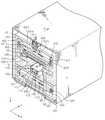
챔버(101)는 속이 빈 상자 형상으로 형성되며, 그 내부에 하나 이상의 유기층 증착 어셈블리(100-1)와 이송부(400)가 수용된다. 이를 다른 측면에서 설명하면, 지면에 고정되도록 풋(foot)(102)이 형성되고, 풋(foot)(102) 상에 하부 하우징(103)이 형성되고, 하부 하우징(103)의 상부에 상부 하우징(104)이 형성된다. 그리고, 챔버(101)는 하부 하우징(103) 및 상부 하우징(104)을 모두 내부에 수용하도록 형성된다. 이때 하부 하우징(103)과 챔버(101)의 연결부는 밀봉처리되어 챔버(101) 내부가 외부와 완전히 차단되도록 할 수 있다. 이와 같이 하부 하우징(103)과 상부 하우징(104)이 지면에 고정된 풋(foot)(102) 상에 형성됨으로써, 챔버(101)가 수축/팽창을 반복하더라도 하부 하우징(103)과 상부 하우징(104)은 고정된 위치를 유지할 수 있으며, 따라서 하부 하우징(103)과 상부 하우징(104)이 증착부(100) 내에서 일종의 기준 프레임(reference frame)의 역할을 수행할 수 있는 것이다.The
한편, 상부 하우징(104)의 내부에는 유기층 증착 어셈블리(100-1)와 이송부(400)의 제1 이송부(410)가 형성되고, 하부 하우징(103)의 내부에는 이송부(400)의 제2 이송부(420)가 형성되는 것으로 기술할 수 있다. 그리고, 이동부(430)가 제1 이송부(410)와 제2 이송부(420) 사이를 순환 이동하면서 연속적으로 증착이 수행되는 것이다.
The organic layer deposition assembly 100-1 and the
이하에서는 유기층 증착 어셈블리(100-1)의 상세 구성에 대하여 설명한다.Hereinafter, the detailed structure of the organic layer deposition assembly 100-1 will be described.
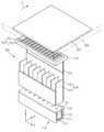
각각의 유기층 증착 어셈블리(100-1)는 증착원(110), 증착원 노즐부(120), 패터닝 슬릿 시트(130), 차단 부재(140), 제1 스테이지(150), 제2 스테이지(160), 촬영 부재(170), 센서(180) 등을 포함한다. 여기서, 도 3 및 도 4의 모든 구성은 적절한 진공도가 유지되는 챔버(101) 내에 배치되는 것이 바람직하다. 이는 증착 물질의 직진성을 확보하기 위함이다.Each organic layer deposition assembly 100-1 includes an
상세히, 증착원(110)에서 방출된 증착 물질(115)이 증착원 노즐부(120) 및 패터닝 슬릿 시트(130)를 통과하여 기판(2)에 원하는 패턴으로 증착되게 하려면, 기본적으로 챔버(미도시) 내부는 FMM 증착 방법과 동일한 고진공 상태를 유지해야 한다. 또한 패터닝 슬릿 시트(130)의 온도가 증착원(110) 온도보다 충분히 낮아야 한다. 왜냐하면, 패터닝 슬릿 시트(130)의 온도가 충분히 낮아야만 온도에 의한 패터닝 슬릿 시트(130)의 열팽창 문제를 최소화할 수 있기 때문이다.In detail, in order for the
이러한 챔버(101) 내에는 피 증착체인 기판(2)이 배치된다. 상기 기판(2)은 평판 표시장치용 기판이 될 수 있는데, 다수의 평판 표시장치를 형성할 수 있는 마더 글라스(mother glass)와 같은 40인치 이상의 대면적 기판이 적용될 수 있다.In this
여기서, 본 발명의 일 실시예에서는, 기판(2)이 유기층 증착 어셈블리(100-1)에 대하여 상대적으로 이동하면서 증착이 진행되는 것을 일 특징으로 한다.Here, in one embodiment of the present invention, the deposition proceeds as the
상세히, 기존 FMM 증착 방법에서는 FMM 크기가 기판 크기와 동일하게 형성되어야 한다. 따라서, 기판 사이즈가 증가할수록 FMM도 대형화되어야 하며, 이로 인해 FMM 제작이 용이하지 않고, FMM을 인장하여 정밀한 패턴으로 얼라인(align) 하기도 용이하지 않다는 문제점이 존재하였다.Specifically, in the conventional FMM deposition method, the FMM size must be formed equal to the substrate size. Therefore, as the substrate size increases, the FMM must be made larger, which makes it difficult to fabricate the FMM, and it is not easy to align the FMM with a precise pattern by pulling the FMM.
이와 같은 문제점을 해결하기 위하여, 본 발명의 일 실시예에 관한 유기층 증착 어셈블리(100-1)는, 유기층 증착 어셈블리(100-1)와 기판(2)이 서로 상대적으로 이동하면서 증착이 이루어지는 것을 일 특징으로 한다. 다시 말하면, 유기층 증착 어셈블리(100-1)와 마주보도록 배치된 기판(2)이 Y축 방향을 따라 이동하면서 연속적으로 증착을 수행하게 된다. 즉, 기판(2)이 도 3의 화살표 A 방향으로 이동하면서 스캐닝(scanning) 방식으로 증착이 수행되는 것이다. 여기서, 도면에는 기판(2)이 챔버(미도시) 내에서 Y축 방향으로 이동하면서 증착이 이루어지는 것으로 도시되어 있으나, 본 발명의 사상은 이에 제한되지 아니하며, 기판(2)은 고정되어 있고 유기층 증착 어셈블리(100-1) 자체가 Y축 방향으로 이동하면서 증착을 수행하는 것도 가능하다 할 것이다.In order to solve such problems, the organic layer deposition assembly 100-1 according to an embodiment of the present invention is configured such that deposition is performed while the organic layer deposition assembly 100-1 and the
따라서, 본 발명의 유기층 증착 어셈블리(100-1)에서는 종래의 FMM에 비하여 훨씬 작게 패터닝 슬릿 시트(130)를 만들 수 있다. 즉, 본 발명의 유기층 증착 어셈블리(100-1)의 경우, 기판(2)이 Y축 방향을 따라 이동하면서 연속적으로, 즉 스캐닝(scanning) 방식으로 증착을 수행하기 때문에, 패터닝 슬릿 시트(130)의 X축 방향 및 Y축 방향의 길이 중 적어도 한 방향의 길이는 기판(2)의 길이보다 훨씬 작게 형성될 수 있는 것이다. 이와 같이, 종래의 FMM에 비하여 훨씬 작게 패터닝 슬릿 시트(130)를 만들 수 있기 때문에, 본 발명의 패터닝 슬릿 시트(130)는 그 제조가 용이하다. 즉, 패터닝 슬릿 시트(130)의 에칭 작업이나, 그 이후의 정밀 인장 및 용접 작업, 이동 및 세정 작업 등 모든 공정에서, 작은 크기의 패터닝 슬릿 시트(130)가 FMM 증착 방법에 비해 유리하다. 또한, 이는 디스플레이 장치가 대형화될수록 더욱 유리하게 된다.Accordingly, the
이와 같이, 유기층 증착 어셈블리(100-1)와 기판(2)이 서로 상대적으로 이동하면서 증착이 이루어지기 위해서는, 유기층 증착 어셈블리(100-1)와 기판(2)이 일정 정도 이격되는 것이 바람직하다. 이에 대하여는 뒤에서 상세히 기술하기로 한다.It is preferable that the organic layer deposition assembly 100-1 and the
한편, 챔버 내에서 상기 기판(2)과 대향하는 측에는, 증착 물질(115)이 수납 및 가열되는 증착원(110)이 배치된다. 상기 증착원(110) 내에 수납되어 있는 증착 물질(115)이 기화됨에 따라 기판(2)에 증착이 이루어진다.On the other hand, on the side facing the
상세히, 증착원(110)은 그 내부에 증착 물질(115)이 채워지는 도가니(111)와, 도가니(111)를 가열시켜 도가니(111) 내부에 채워진 증착 물질(115)을 도가니(111)의 일 측, 상세하게는 증착원 노즐부(120) 측으로 증발시키기 위한 히터(112)를 포함한다.In detail, the
증착원(110)의 일 측, 상세하게는 증착원(110)에서 기판(2)을 향하는 측에는 증착원 노즐부(120)가 배치된다. 여기서, 본 발명에 따른 유기층 증착 어셈블리는 공통층과 패턴층을 증착하는데 있어서 증착원 노즐이 서로 상이하게 형성될 수도 있다. 즉, 도면에는 도시되지 않았지만, 패턴층을 형성하기 위한 증착원 노즐부에는 Y축 방향 즉 기판(2)의 스캔 방향을 따라서 복수 개의 증착원 노즐(121)들이 형성될 수 있다. 이에 따라, X축 방향으로는 증착원 노즐(121)이 하나만 존재하도록 증착원 노즐(121)을 형성함으로써, 음영(shadow)의 발생을 크게 감소시킬 수 있는 것이다. 반면, 공통층을 형성하기 위한 증착원 노즐부에는 X축 방향을 따라서 복수 개의 증착원 노즐(121)들이 형성될 수 있다. 이에 의해 공통층의 두께 균일도를 향상시킬 수 있는 것이다.The evaporation
한편, 증착원(110)과 기판(2) 사이에는 패터닝 슬릿 시트(130)가 더 구비된다. 패터닝 슬릿 시트(130)는 대략 창문 틀과 같은 형태로 형성되는 프레임(135)을 더 포함하며, 패터닝 슬릿 시트(130)에는 X축 방향을 따라서 복수 개의 패터닝 슬릿(131)들이 형성된다. 증착원(110) 내에서 기화된 증착 물질(115)은 증착원 노즐부(120) 및 패터닝 슬릿 시트(130)를 통과하여 피 증착체인 기판(2) 쪽으로 향하게 되는 것이다. 이때, 상기 패터닝 슬릿 시트(130)는 종래의 파인 메탈 마스크(FMM) 특히 스트라이프 타입(stripe type)의 마스크의 제조 방법과 동일한 방법인 에칭을 통해 제작될 수 있다. 이때, 증착원 노즐(121)들의 총 개수보다 패터닝 슬릿(131)들의 총 개수가 더 많게 형성될 수도 있다.A
여기서, 상술한 증착원(110)(및 이와 결합된 증착원 노즐부(120))과 패터닝 슬릿 시트(130)는 서로 일정 정도 이격되도록 형성될 수 있다.Here, the deposition source 110 (and the deposition
상술한 바와 같이, 본 발명의 일 실시예에 관한 유기층 증착 어셈블리(100-1)는 기판(2)에 대하여 상대적으로 이동하면서 증착을 수행하며, 이와 같이 유기층 증착 어셈블리(100-1)가 기판(2)에 대하여 상대적으로 이동하기 위해서 패터닝 슬릿 시트(130)는 기판(2)으로부터 일정 정도 이격되도록 형성된다.As described above, the organic layer deposition assembly 100-1 according to one embodiment of the present invention performs deposition while moving relative to the
상세히, 종래의 FMM 증착 방법에서는 기판에 음영(shadow)이 생기지 않도록 하기 위하여 기판에 마스크를 밀착시켜서 증착 공정을 진행하였다. 그러나, 이와 같이 기판에 마스크를 밀착시킬 경우, 기판과 마스크 간의 접촉에 의한 불량 문제가 발생한다는 문제점이 존재하였다. 또한, 마스크를 기판에 대하여 이동시킬 수 없기 때문에, 마스크가 기판과 동일한 크기로 형성되어야 한다. 따라서, 디스플레이 장치가 대형화됨에 따라 마스크의 크기도 커져야 하는데, 이와 같은 대형 마스크를 형성하는 것이 용이하지 아니하다는 문제점이 존재하였다.In detail, in the conventional FMM deposition method, a mask is closely adhered to a substrate to prevent a shadow from being formed on the substrate, and a deposition process is performed. However, when the mask is brought into close contact with the substrate in this manner, there is a problem that a problem of defective due to contact between the substrate and the mask occurs. Further, since the mask can not be moved relative to the substrate, the mask must be formed to have the same size as the substrate. Therefore, as the size of the display device is increased, the size of the mask must be increased. Thus, there is a problem that it is not easy to form such a large mask.
이와 같은 문제점을 해결하기 위하여, 본 발명의 일 실시예에 관한 유기층 증착 어셈블리(100-1)에서는 패터닝 슬릿 시트(130)가 피 증착체인 기판(2)과 소정 간격을 두고 이격되도록 배치되도록 한다.In order to solve such a problem, in the organic layer deposition assembly 100-1 according to an embodiment of the present invention, the
이와 같은 본 발명에 의해서 마스크를 기판보다 작게 형성한 후, 마스크를 기판에 대하여 이동시키면서 증착을 수행할 수 있게 됨으로써, 마스크 제작이 용이해지는 효과를 얻을 수 있다. 또한, 기판과 마스크 간의 접촉에 의한 불량을 방지하는 효과를 얻을 수 있다. 또한, 공정에서 기판과 마스크를 밀착시키는 시간이 불필요해지기 때문에, 제조 속도가 향상되는 효과를 얻을 수 있다.
According to the present invention, after the mask is formed smaller than the substrate, the deposition can be performed while moving the mask relative to the substrate, so that it is possible to obtain an effect of facilitating the production of the mask. In addition, it is possible to obtain an effect of preventing defects due to contact between the substrate and the mask. Further, since the time required for the substrate and the mask to adhere to each other in the process becomes unnecessary, an effect of improving the manufacturing speed can be obtained.
다음으로, 상부 하우징(104) 내에서의 각 구성요소의 구체적인 배치는 다음과 같다.Next, the specific arrangement of each component in the
먼저, 상부 하우징(104)의 바닥 부분에는 상술한 증착원(110) 및 증착원 노즐부(120)가 배치된다. 그리고, 증착원(110) 및 증착원 노즐부(120)의 양측에는 안착부(104-1)가 돌출 형성되며, 안착부(104-1) 상에는 제1 스테이지(150), 제2 스테이지(160) 및 상술한 패터닝 슬릿 시트(130)가 차례로 형성된다.First, the
여기서, 제1 스테이지(150)는 X축 방향 및 Y축 방향으로 이동 가능하도록 형성되어, 패터닝 슬릿 시트(130)를 X축 방향 및 Y축 방향으로 얼라인 하는 기능을 수행한다. 즉, 제1 스테이지(150)는 복수 개의 액츄에이터를 구비하여, 상부 하우징(104)에 대하여 제1 스테이지(150)가 X축 방향 및 Y축 방향으로 이동하도록 형성되는 것이다.Here, the
한편, 제2 스테이지(160)는 Z축 방향으로 이동 가능하도록 형성되어, 패터닝 슬릿 시트(130)를 Z축 방향으로 얼라인 하는 기능을 수행한다. 즉, 제2 스테이지(160)는 복수 개의 액츄에이터를 구비하여, 제1 스테이지(150)에 대하여 제2 스테이지(160)가 Z축 방향으로 이동하도록 형성되는 것이다.Meanwhile, the
한편, 제2 스테이지(160) 상에는 패터닝 슬릿 시트(130)가 형성된다. 이와 같이, 패터닝 슬릿 시트(130)가 제1 스테이지(150) 및 제2 스테이지(160) 상에 형성되어 패터닝 슬릿 시트(130)가 X축 방향, Y축 방향 및 Z축 방향으로 이동 가능하도록 형성됨으로써, 기판(2)과 패터닝 슬릿 시트(130) 간의 얼라인, 특히 리얼타임 얼라인(real-time align)을 수행할 수 있는 것이다.On the other hand, a
나아가 상부 하우징(104), 제1 스테이지(150) 및 제2 스테이지(160)는 증착원 노즐(121)을 통해 배출되는 증착 물질이 분산되지 않도록 증착 물질의 이동 경로를 가이드 하는 역할을 동시에 수행할 수 있다. 즉, 상부 하우징(104), 제1 스테이지(150) 및 제2 스테이지(160)에 의해 증착 물질의 경로가 밀폐되어 증착 물질의 X축 방향 및 Y축 방향 이동을 동시에 가이드 할 수도 있다.Further, the
한편, 패터닝 슬릿 시트(130)와 증착원(110) 사이에는 차단 부재(140)가 더 구비될 수도 있다. 상세히, 기판(2)의 테두리 부분에는 애노드 전극 또는 캐소드 전극 패턴이 형성되어, 향후 제품 검사용 또는 제품 제작시 단자로 활용하기 위한 영역이 존재한다. 만약 이 영역에 유기물이 성막이 될 경우, 애노드 전극 또는 캐소드 전극이 제 역할을 하기 어렵데 되며, 따라서 이와 같은 기판(2)의 테두리 부분은 유기물 등이 성막되지 않아야 하는 비성막 영역이 되어야 한다. 그러나 상술한 바와 같이, 본 발명의 박막 증착 장치에서는 기판(2)이 박막 증착 장치에 대하여 이동하면서 스캐닝(scanning) 방식으로 증착이 수행되므로, 기판(2)의 비성막 영역에 유기물 증착을 방지하는 것이 용이하지 않았다.A blocking
이와 같이 기판(2)의 비성막 영역에 유기물이 증착되는 것을 방지하기 위하여, 본 발명의 일 실시예에 관한 박막 증착 장치에서는 기판(2)의 테두리 부분에 별도의 차단 부재(140)가 더 구비될 수 있다. 도면에는 상세히 도시되지 않았지만, 차단 부재(140)는 서로 이웃한 두 개의 플레이트로 구성될 수 있다.In order to prevent organic substances from being deposited on the non-deposited region of the
기판(2)이 유기층 증착 어셈블리(100-1)를 통과하지 아니할 때에는, 차단 부재(140)가 증착원(110)을 가림으로써, 증착원(110)에서 발산된 증착 물질(115)이 패터닝 슬릿 시트(130)에 묻지 않도록 한다. 이 상태에서 기판(2)이 유기층 증착 어셈블리(100-1)로 진입하기 시작하면, 증착원(110)을 가리고 있던 전방의 차단 부재(140)가 기판(2)의 이동과 함께 이동하면서 증착 물질의 이동 경로가 오픈되어, 증착원(110)에서 발산된 증착 물질(115)이 패터닝 슬릿 시트(130)를 통과하여 기판(2)에 증착된다. 한편, 기판(2) 전체가 유기층 증착 어셈블리(100-1)를 통과하면, 후방의 차단 부재(140)가 기판(2)의 이동과 함께 이동하면서 증착 물질의 이동 경로를 다시 폐쇄하여 증착원(110)을 가림으로써, 증착원(110)에서 발산된 증착 물질(115)이 패터닝 슬릿 시트(130)에 묻지 않도록 한다.When the
이와 같은 차단 부재(140)에 의해서 기판(2)의 비성막 영역이 가려짐으로써, 별도의 구조물 없이도 간편하게 기판(2)의 비성막 영역에 유기물이 증착되는 것이 방지되는 효과를 얻을 수 있다.
The blocking
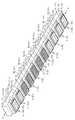
이하에서는 피증착체인 기판(2)을 이송하는 이송부(400)에 대하여 상세히 설명하도록 한다. 도 3 및 도 4를 참조하면, 이송부(400)는 제1 이송부(410)와, 제2 이송부(420)와, 이동부(430)를 포함한다.Hereinafter, the
제1 이송부(410)는 유기층 증착 어셈블리(100-1)에 의해 기판(2) 상에 유기층이 증착될 수 있도록, 캐리어(431) 및 이와 결합된 정전 척(432)을 포함하는 이동부(430)와, 이동부(430)에 부착되어 있는 기판(2)을 인라인(in-line)으로 이송하는 역할을 수행한다. 이와 같은 제1 이송부(410)는 코일(411), 가이드부(412), 상면 자기부상 베어링(413), 측면 자기부상 베어링(414), 갭 센서(415)(416)를 포함한다.The
제2 이송부(420)는 증착부(100)을 통과하면서 1회의 증착이 완료된 후 언로딩부(300)에서 기판(2)이 분리된 이동부(430)를 로딩부(200)로 회송하는 역할을 수행한다. 이와 같은 제2 이송부(420)는 코일(421), 롤러 가이드(422) 및 차징 트랙(charging track)(423)을 포함한다.The
이동부(430)는 제1 이송부(410) 및 제2 이송부(420)를 따라 이송되는 캐리어(431)와, 캐리어(431)의 일 면상에 결합되며 기판(2)이 부착되는 정전 척(432)을 포함한다.The moving
이하에서는 이송부(400)의 각 구성요소에 대하여 더욱 상세히 설명한다.Hereinafter, each component of the
먼저, 이동부(430)의 캐리어(431)에 대해 상세히 설명한다.First, the
캐리어(431)는 본체부(431a), LMS 마그넷(Linear motor system Magnet)(431b), CPS 모듈(Contactless power supply Module)(431c), 전원부(431d) 및 가이드 홈(431e)을 포함한다.The
본체부(431a)는 캐리어(431)의 기저부를 이루며, 철과 같은 자성체로 형성될 수 있다. 이와 같은 캐리어(431)의 본체부(431a)와 후술할 자기부상 베어링(413)(414)과의 척력에 의하여 캐리어(431)가 가이드부(412)에 대해 일정 정도 이격된 상태를 유지할 수 있다.The
본체부(431a)의 양측면에는 가이드 홈(431e)이 형성될 수 있으며, 이와 같은 가이드 홈(431e) 내에는 가이드부(412)의 가이드 돌기(412e)가 수용될 수 있다.Guide grooves 431e may be formed on both sides of the
본체부(431a)의 진행방향의 중심선을 따라 마그네틱 레일(431b)이 형성될 수 있다. 본체부(431a)의 마그네틱 레일(431b)과 후술할 코일(411)이 결합하여 리니어 모터를 구성할 수 있으며, 이와 같은 리니어 모터에 의하여 캐리어(431)가 A방향으로 이송될 수 있는 것이다.A
본체부(431a)에서 마그네틱 레일(431b)의 일 측에는 CPS 모듈(431c) 및 전원부(431d)가 각각 형성될 수 있다. 전원부(431d)는 정전 척(432)이 기판(2)을 척킹(chucking)하고 이를 유지할 수 있도록 전원을 제공하기 위한 일종의 충전용 배터리이며, CPS 모듈(431c)은 전원부(431d)를 충전하기 위한 무선 충전 모듈이다. 상세히, 후술할 제2 이송부(420)에 형성된 차징 트랙(charging track)(423)은 인버터(inverter)(미도시)와 연결되어, 캐리어(431)가 제2 이송부(420) 내에서 이송될 때, 차징 트랙(charging track)(423)과 CPS 모듈(431c) 사이에 자기장이 형성되어 CPS 모듈(431c)에 전력을 공급한다. 그리고, CPS 모듈(431c)에 공급된 전력은 전원부(431d)를 충전하게 되는 것이다.A
한편, 정전척(Electro Static Chuck, 432)은 세라믹으로 구비된 본체의 내부에 전원이 인가되는 전극이 매립된 것으로, 이 전극에 고전압이 인가됨으로써 본체의 표면에 기판(2)을 부착시키는 것이다.
The
다음으로, 이동부(430)의 구동에 대해 상세히 설명한다.Next, the driving of the moving
본체부(431a)의 마그네틱 레일(431b)과 코일(411)이 결합하여 구동부를 구성할 수 있다. 여기서, 구동부는 리니어 모터(Linear Motor)일 수 있다. 리니어 모터는 종래의 미끄럼 안내 시스템에 비하여 마찰 계수가 작고 위치 오차가 거의 발생하지 않아 위치 결정도가 매우 높은 장치이다. 상술한 바와 같이, 리니어 모터는 코일(411)과 마그네틱 레일(431b)로 이루어질 수 있으며, 마그네틱 레일(431b)이 캐리어(431) 상에 일렬로 배치되고, 코일(411)은 마그네틱 레일(431b)과 마주보도록 챔버(101) 내의 일 측에 다수 개가 일정 간격으로 배치될 수 있다. 이와 같이 이동 물체인 캐리어(431)에 코일(411)이 아닌 마그네틱 레일(431b)이 배치되므로 캐리어(431)에 전원을 인가하지 않아도 캐리어(431)의 구동이 가능해질 수 있다. 여기서, 코일(411)은 ATM 상자(atmosphere box) 내에 형성되어 대기 상태에 설치되고, 마그네틱 레일(431b)은 캐리어(431)에 부착되어 진공인 챔버(101) 내에서 캐리어(431)가 주행할 수 있게 되는 것이다.
The
다음으로, 제1 이송부(410) 및 이동부(430)에 대해 상세히 설명한다.Next, the
도 4를 참조하면, 제1 이송부(410)는 기판(2)을 고정하고 있는 정전 척(432) 및 이를 이송하는 캐리어(431)를 이동시키는 역할을 수행한다. 여기서, 제1 이송부(410)는 코일(411), 가이드부(412), 상면 자기부상 베어링(413), 측면 자기부상 베어링(414), 갭 센서(415)(416)를 포함한다.Referring to FIG. 4, the
코일(411)과 가이드부(412)는 각각 상부 하우징(104)의 내부면에 형성되며, 이중 코일(411)은 상부 하우징(104)의 상측 내부면에 형성되고, 가이드부(412)는 상부 하우징(104)의 양측 내부면에 형성된다.The
가이드부(412)는 캐리어(431)가 일 방향으로 이동되도록 가이드하는 역할을 수행한다. 이때, 가이드부(412)는 증착부(100)를 관통하도록 형성된다.The
측면 자기부상 베어링(414)은 캐리어(431)의 양 측면에 대응되도록 가이드부(412) 내에 각각 배치된다. 측면 자기부상 베어링(414)은 캐리어(431)와 가이드부(412) 사이의 간격을 발생시켜, 캐리어(431)가 이동할 때 가이드부(412)와 접촉되지 않고 비접촉 방식으로 가이드부(412)를 따라 이동하도록 하는 역할을 한다. 즉, 좌측의 측면 자기부상 베어링(414)과 자성체인 캐리어(431) 사이에 발생하는 척력과, 우측의 측면 자기부상 베어링(414)과 자성체인 캐리어(431) 사이에 발생하는 척력이 서로 평형을 이루면서 캐리어(431)와 가이드부(412) 사이의 간격을 발생시키는 동시에 그 간격을 일정하게 유지하는 것이다.The side magnetic levitation bearings 414 are respectively disposed in the
한편, 상부 자기부상 베어링(413)은 캐리어(431)의 상부에 위치하도록 가이드부(412) 내에 각각 배치된다. 상부 자기부상 베어링(413)은 캐리어(431)가 제1 수용부(412a) 및 제2 수용부(412b)에 접촉하지 않고 이들과 일정한 간격을 유지하면서 가이드부(412)를 따라 이동하도록 하는 역할을 한다. 즉, 상부 자기부상 베어링(413)과 자성체인 캐리어(431) 사이에 발생하는 척력과 중력이 서로 평행을 이루면서 캐리어(431)와 가이드부(412) 사이의 간격을 발생시키는 동시에 그 간격을 일정하게 유지하는 것이다.On the other hand, the upper magnetic levitation bearings 413 are disposed in the
가이드부(412)는 갭 센서(415)를 더 구비할 수 있다. 갭 센서(415)는 캐리어(431)과 가이드부(412) 사이의 간격을 측정할 수 있다. 또한, 측면 자기부상 베어링(414)의 일 측에도 갭 센서(416)가 배치될 수 있다. 측면 자기부상 베어링(414)에 배치된 갭 센서(416)는 캐리어(431)의 측면과 측면 자기부상 베어링(414) 사이의 간격을 측정할 수 있다.The
갭 센서(415)(416)에 의해 측정된 값에 따라 자기부상 베어링(413)(414)의 자기력이 변경되어 캐리어(431)와 가이드부(412) 사이의 간격이 실시간으로 조절될 수 있다. 즉, 자기부상 베어링(413)(414)과 갭 센서(415)(416)를 이용한 피드백 제어에 의해 캐리어(431)의 정밀 이동이 가능하다.
The magnetic force of the magnetic levitation bearings 413 and 414 is changed in accordance with the value measured by the gap sensors 415 and 416 so that the interval between the
다음으로, 제2 이송부(420) 및 이동부(430)에 대해 상세히 설명한다.Next, the
다시 도 4를 참조하면, 제2 이송부(420)는 언로딩부(300)에서 기판이 분리되고 난 이후의 정전 척(432) 및 이를 이송하는 캐리어(431)를 다시 로딩부(200)로 이동시키는 역할을 수행한다. 여기서, 제2 이송부(420)는 코일(421), 롤러 가이드(422), 차징 트랙(charging track)(423)을 포함한다.4, the
상세히, 코일(421), 롤러 가이드(422) 및 차징 트랙(423)은 각각 하부 하우징(103)의 내부면에 형성되며, 이중 코일(421)과 차징 트랙(423)은 하부 하우징(103)의 상측 내부면에 형성되고, 롤러 가이드(422)는 하부 하우징(103)의 양측 내부면에 형성된다. 여기서, 코일(421)은 제1 이송부(410)의 코일(411)과 마찬가지로 ATM 상자(atmosphere box) 내에 형성될 수 있다.In detail, the
한편, 제1 이송부(410)와 마찬가지로 제2 이송부(420) 역시 코일(421)을 구비하며, 캐리어(431)의 본체부(431a)의 마그네틱 레일(431b)과 코일(421)이 결합하여 구동부를 구성할 수 있으며, 여기서 구동부는 리니어 모터(Linear Motor)일 수 있다. 이와 같은 리니어 모터(Linear Motor)에 의해서 캐리어(431)가 도 3의 A방향의 반대 방향을 따라 이동할 수 있다.Similarly to the
한편, 롤러 가이드(422)는 캐리어(431)가 일 방향으로 이동되도록 가이드하는 역할을 수행한다. 이때, 롤러 가이드(422)는 증착부(100)를 관통하여 형성된다.Meanwhile, the
결과적으로, 제2 이송부(420)는 기판에 유기물을 증착하는 단계가 아닌, 비어있는 캐리어(431)를 회송하는 단계이기 때문에, 제1 이송부(410)에 비해 위치 정밀도가 크게 요구되지 아니한다. 따라서, 높은 위치 정밀도가 요구되는 제1 이송부(410)에는 자기 부상을 적용하여 위치 정밀도를 확보하고, 상대적으로 낮은 위치 정밀도가 요구되는 제2 이송부(420)에는 종래의 롤러 방식을 적용하여 제조 단가를 낮추고 유기층 증착 장치의 구성을 간결하게 하는 것이다. 물론, 도면에는 도시되지 않았지만, 제2 이송부(420)에도 제1 이송부(410)와 마찬가지로 자기 부상을 적용하는 것도 가능하다 할 것이다.
As a result, the position of the
한편, 본 발명의 일 실시예에 따른 유기층 증착 장치(1)의 유기층 증착 어셈블리(100-1)는 얼라인(align)을 위한 카메라(170) 및 센서(180)를 더 구비할 수 있다. 상세히, 카메라(170)는 패터닝 슬릿 시트(130)의 프레임(155)에 형성된 제1마크(미도시)와 기판(2)에 형성된 제2 마크(미도시)를 실시간으로 얼라인할 수 있다. 여기서, 카메라(170)는 증착이 진행중인 진공 챔버(101) 내에서 원활한 시야 확보를 할 수 있도록 구비된다. 이를 위해, 카메라(170)는 카메라 수용부(171) 내에 형성되어 대기 상태에 설치될 수 있다.The organic layer deposition assembly 100-1 of the organic layer deposition apparatus 1 according to an embodiment of the present invention may further include a
한편, 본 발명에서는 기판(2)과 패터닝 슬릿 시트(130)가 일정 정도 이격되어 있는바, 하나의 카메라(170)를 이용하여, 서로 다른 위치에 있는 기판(2)까지의 거리와 패터닝 슬릿 시트(130)까지의 거리를 함께 측정하여야 한다. 이를 위해, 본 발명의 일 실시예에 따른 유기층 증착 장치(1)의 유기층 증착 어셈블리(100-1)는 센서(180)를 구비할 수 있다. 여기서, 센서(180)는 공초점 센서(Confocal sensor)일 수 있다. 공초점 센서는 고속으로 회전하는 스캐닝 미러(scanning mirror)를 이용하여 레이저 빔으로 측정 대상을 스캐닝하고 레이저 빔에 의해 발광된 형광 또는 반사광선을 이용하여 측정대상까지의 거리를 측정할 수 있다. 공초점 센서는 서로 다른 매질 사이의 경계면을 감지하여 거리를 측정할 수 있다.In the present invention, since the
이와 같이 카메라(170) 및 센서(180)를 구비하여, 실시간으로 기판(2)과 패터닝 슬릿 시트(130) 간의 간격을 측정하는 것이 가능해지고 따라서 실시간으로 기판(2)과 패터닝 슬릿 시트(130)를 얼라인 하는 것이 가능해짐으로써, 패턴의 위치 정밀도가 더욱 향상되는 효과를 얻을 수 있다.
The distance between the
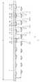
도 5는 패턴층을 형성하기 위한 증착원 노즐을 나타내는 사시도이고, 도 6은 공통층을 형성하기 위한 증착원 노즐을 나타내는 사시도이다. 패턴층을 형성하는 유기층 증착 어셈블리는 패턴층 증착 어셈블리(도 7의 100-5, ..., 100-9)이며, 공통층을 형성하는 유기층 증착 어셈블리는 공통층 증착 어셈블리(100-1, ..., 100-4, 100-10, 100-11)이다.Fig. 5 is a perspective view showing an evaporation source nozzle for forming a pattern layer, and Fig. 6 is a perspective view showing an evaporation source nozzle for forming a common layer. The organic layer deposition assemblies forming the pattern layer are pattern layer deposition assemblies (100-5, ..., 100-9 in FIG. 7), and the organic layer deposition assemblies forming the common layer are the common layer deposition assemblies 100-1,. .., 100-4, 100-10, 100-11).
먼저 도 5를 참조하면, 패턴층 증착 어셈블리(100-5) 내에는 세 개의 증착원(110)과 세 개의 증착원 노즐부(120)가 배치되며, 각각의 증착원 노즐부(120)에는 그 중심부에 하나의 증착원 노즐(121)이 형성된다. 그리고, 이와 같이 증착원(110) 내에서 기화된 증착 물질(115)은 증착원 노즐부(120)를 통과하여 피 증착체인 기판(2) 쪽으로 향하게 되는 것이다. 이와 같이, 증착원 노즐부(120) 상에 하나의 증착원 노즐(121)이 형성되고, 또한 하나의 패턴층 증착 어셈블리(100-5) 내에는 세 개의 증착원(110)이 기판(2)의 스캔 방향을 따라 배치되어, 결과적으로 하나의 패턴층 증착 어셈블리(100-5) 내에는 기판(2)의 스캔 방향을 따라서 복수 개의 증착원 노즐(121)들이 형성된다. 이 경우, X축 방향에 있어서 증착원 노즐(121)이 복수 개 구비된다면, 각 증착원 노즐(121)과 패터닝 슬릿(151)과의 거리가 각각 상이하게 되며, 이때 패터닝 슬릿(151)과 거리가 먼 증착원 노즐(121)에서 발산된 증착 물질에 의해 음영(shadow)이 발생하게 된다. 따라서, 본 발명과 같이 X축 방향으로는 증착원 노즐(121)이 하나만 존재하도록 증착원 노즐(121)을 형성함으로써, 음영(shadow)의 발생을 크게 감소시킬 수 있는 것이다. 또한, 다수 개의 증착원 노즐(121)들이 스캔 방향으로 존재하므로, 개별 증착원 노즐 간 플럭스(flux) 차이가 발생하여도 그 차이가 상쇄되어 증착 균일도가 일정하게 유지되는 효과를 얻을 수 있다.5, three
그리고, 도면에는 도시되지 않았지만, 하나의 패턴층 증착 어셈블리(100-5) 내에 배치된 세 개의 증착원(110) 중 양단의 증착원들은 호스트 물질을 증착하고, 가운데 배치된 증착원은 도펀트 물질을 증착할 수 있다. 이와 같이 본 발명의 유기층 증착 장치는 호스트 물질을 증착하는 증착원과 도펀트 물질을 증착하는 증착원을 함께 구비하여, 기판(2)상에 호스트 물질과 도펀트 물질을 동시에 증착할 수 있도록 함으로써, 공정이 더욱 간단하고 빨라지며, 소자 효율 또한 향상되는 효과를 얻을 수 있다.Although not shown in the drawing, the evaporation sources at both ends of the three
한편, 도 6을 참조하면, 증착원(110')의 일 측, 상세하게는 증착원(110')에서 기판(2)을 향하는 측에는 증착원 노즐부(120')가 배치된다. 그리고, 증착원 노즐부(120')에는, X축 방향(즉 기판(2)의 스캔 방향과 수직인 방향)을 따라서 복수 개의 증착원 노즐(121')들이 형성된다. 여기서, 상기 복수 개의 증착원 노즐(121')들은 등 간격으로 형성될 수도 있고, 양단부로 갈수록 간격이 좁아지도록 형성될 수도 있다. 증착원(110') 내에서 기화된 증착 물질은 이와 같은 증착원 노즐부(120')의 증착원 노즐(121')들을 통과하여 피 증착체인 기판(2) 쪽으로 향하게 되는 것이다. 이와 같이 공통층을 증착하는데 있어서는 X축 방향(즉 기판(2)의 스캔 방향과 수직인 방향)을 따라서 복수 개의 증착원 노즐(121')들을 형성함으로써, 공통층의 두께 균일도를 향상시킬 수 있는 것이다.
Referring to FIG. 6, an evaporation source nozzle unit 120 'is disposed on one side of the evaporation source 110', specifically, on a side of the evaporation source 110 'that faces the
한편, 증착원(110)과 기판(2) 사이에는 패터닝 슬릿 시트(130)가 더 구비된다. 패터닝 슬릿 시트(130)는 대략 창문 틀과 같은 형태로 형성되는 프레임(135)을 더 포함하며, 패터닝 슬릿 시트(130)에는 X축 방향을 따라서 복수 개의 패터닝 슬릿(131)들이 형성된다. 증착원(110) 내에서 기화된 증착 물질(115)은 증착원 노즐부(120) 및 패터닝 슬릿 시트(130)를 통과하여 피 증착체인 기판(2) 쪽으로 향하게 되는 것이다. 이때, 상기 패터닝 슬릿 시트(130)는 종래의 파인 메탈 마스크(FMM) 특히 스트라이프 타입(stripe type)의 마스크의 제조 방법과 동일한 방법인 에칭을 통해 제작될 수 있다. 이때, 증착원 노즐(121)들의 총 개수보다 패터닝 슬릿(131)들의 총 개수가 더 많게 형성될 수도 있다.A
여기서, 상술한 증착원(110) 및 이와 결합된 증착원 노즐부(120))과 패터닝 슬릿 시트(130)는 서로 일정 정도 이격되도록 형성될 수 있다.Here, the
상술한 바와 같이, 본 발명의 일 실시예에 관한 유기층 증착 어셈블리(100-1)는 기판(2)에 대하여 상대적으로 이동하면서 증착을 수행하며, 이와 같이 유기층 증착 어셈블리(100-1)가 기판(2)에 대하여 상대적으로 이동하기 위해서 패터닝 슬릿 시트(130)는 기판(2)으로부터 일정 정도 이격되도록 형성된다.As described above, the organic layer deposition assembly 100-1 according to one embodiment of the present invention performs deposition while moving relative to the
상세히, 종래의 FMM 증착 방법에서는 기판에 음영(shadow)이 생기지 않도록 하기 위하여 기판에 마스크를 밀착시켜서 증착 공정을 진행하였다. 그러나, 이와 같이 기판에 마스크를 밀착시킬 경우, 기판과 마스크 간의 접촉에 의한 불량 문제가 발생한다는 문제점이 존재하였다. 또한, 마스크를 기판에 대하여 이동시킬 수 없기 때문에, 마스크가 기판과 동일한 크기로 형성되어야 한다. 따라서, 디스플레이 장치가 대형화됨에 따라 마스크의 크기도 커져야 하는데, 이와 같은 대형 마스크를 형성하는 것이 용이하지 아니하다는 문제점이 존재하였다.In detail, in the conventional FMM deposition method, a mask is closely adhered to a substrate to prevent a shadow from being formed on the substrate, and a deposition process is performed. However, when the mask is brought into close contact with the substrate in this manner, there is a problem that a problem of defective due to contact between the substrate and the mask occurs. Further, since the mask can not be moved relative to the substrate, the mask must be formed to have the same size as the substrate. Therefore, as the size of the display device is increased, the size of the mask must be increased. Thus, there is a problem that it is not easy to form such a large mask.
이와 같은 문제점을 해결하기 위하여, 본 발명의 일 실시예에 관한 유기층 증착 어셈블리(100-1)에서는 패터닝 슬릿 시트(130)가 피 증착체인 기판(2)과 소정 간격을 두고 이격되도록 배치되도록 한다.In order to solve such a problem, in the organic layer deposition assembly 100-1 according to an embodiment of the present invention, the
이와 같은 본 발명에 의해서 마스크를 기판보다 작게 형성한 후, 마스크를 기판에 대하여 이동시키면서 증착을 수행할 수 있게 됨으로써, 마스크 제작이 용이해지는 효과를 얻을 수 있다. 또한, 기판과 마스크 간의 접촉에 의한 불량을 방지하는 효과를 얻을 수 있다. 또한, 공정에서 기판과 마스크를 밀착시키는 시간이 불필요해지기 때문에, 제조 속도가 향상되는 효과를 얻을 수 있다.
According to the present invention, after the mask is formed smaller than the substrate, the deposition can be performed while moving the mask relative to the substrate, so that it is possible to obtain an effect of facilitating the production of the mask. In addition, it is possible to obtain an effect of preventing defects due to contact between the substrate and the mask. Further, since the time required for the substrate and the mask to adhere to each other in the process becomes unnecessary, an effect of improving the manufacturing speed can be obtained.
도 7은 증착원을 구비한 증착 어셈블리들을 개략적으로 도시한 사시도이다.7 is a perspective view schematically showing deposition assemblies having an evaporation source.
도 7을 참조하면, 본 발명의 일 실시예에 따른 유기층 증착 장치는 11개의 유기층 증착 어셈블리들(100-1, 100-2, ..., 100-11)로 이루어질 수 있다. 또한, 각각의 증착 어셈블리들(100-1, 100-2, ..., 100-11)은 3개의 증착원으로 이루어질 수 있다. 예를 들면, 증착 어셈블리(100-1)는 3개의 증착원(110-1a, 110-1b, 110-1c)을 포함하며, 증착 어셈블리(100-2)는 3개의 증착원(110-2a, 110-2b, 110-2c)을 포함할 수 있다.Referring to FIG. 7, an organic layer deposition apparatus according to an embodiment of the present invention may include eleven organic layer deposition assemblies 100-1, 100-2,..., 100-11. Further, each of the deposition assemblies 100-1, 100-2, ..., and 100-11 may be formed of three evaporation sources. For example, the deposition assembly 100-1 includes three evaporation sources 110-1a, 110-1b, and 110-1c, and the deposition assembly 100-2 includes three evaporation sources 110-2a, 110-2b, 110-2c.
유기층 증착 어셈블리들(100-1, 100-2, ..., 100-11)은 상술한 바와 같이 공통층 증착 어셈블리(100-1, ..100-4, 100-10, 100-11)와 패턴층 증착 어셈블리(100-5, ..., 100-9)로 이루어질 수 있다.Organic layer deposition assemblies 100-1, 100-2, ..., 100-11 may be fabricated using common layer deposition assemblies 100-1, 100-4, 100-10, 100-11, Pattern layer deposition assemblies 100-5, ..., 100-9.
공통층 증착 어셈블리들(100-1, 100-2, 100-3, 100-4, 100-5, 100-10, 100-11) 각각은 유기층(도 15의 63)에서 공통층을 형성할 수 있다. 즉, 공통층 증착 어셈블리(100-1)의 증착원들(110-1a, 110-1b, 110-1c)는 홀 주입층을 형성하는 증착 물질을 구비할 수 있으며, 공통층 증착 어셈블리(100-2)의 증착원들(110-2a, 110-2b, 110-2c)는 버퍼층을 형성하는 증착 물질을 구비할 수 있으며, 공통층 증착 어셈블리(100-3)의 증착원들(110-3a, 110-3b, 110-3c)는 홀 수송층을 형성하는 증착 물질을 구비할 수 있으며, 공통층 증착 증착 어셈블리(100-4)의 증착원들(110-4a, 110-4b, 110-4c)는 홀 주입층을 형성하는 증착 물질을 구비할 수 있다. 또한, 공통층 증착 어셈블리(100-10)의 증착원들(110-10a, 110-10b, 110-10c)는 전공 수송층을 형성하는 증착 물질을 구비할 수 있으며, 공통층 증착 어셈블리(100-11)의 증착원들(110-11a, 110-11b, 110-11c)는 전공 주입층을 형성하는 증착 물질을 구비할 수 있다. 공통층 증착 어셈블리들(100-1, 100-2, 100-3, 100-4, 100-5, 100-10, 100-11)에 의해 형성되는 증착층들은 서브 픽셀에 관계없이 모두 공통적으로 형성될 수 있다. 따라서, 일부 증착 어셈블리들(100-1, 100-2, 100-3, 100-4, 100-5, 100-10, 100-11)의 증착원들 상에는 패터닝 슬릿이 한 개 형성된 패터닝 슬릿 시트, 즉 오픈 마스크(136)가 배치될 수 있다.Each of the common layer deposition assemblies 100-1, 100-2, 100-3, 100-4, 100-5, 100-10, and 100-11 can form a common layer in the organic layer (63 in FIG. 15) have. That is, the evaporation sources 110-1a, 110-1b, and 110-1c of the common layer deposition assembly 100-1 may include evaporation materials forming the hole injection layer, and the common layer deposition assembly 100- The evaporation sources 110-2a, 110-2b, and 110-2c of the common layer deposition assembly 100-3 may include evaporation materials that form a buffer layer, and the evaporation sources 110-3a, 110-3b and 110-3c may comprise a deposition material forming a hole transport layer and the deposition sources 110-4a, 110-4b, 110-4c of the common layer deposition deposition assembly 100-4 And a deposition material for forming a hole injection layer. In addition, the evaporation sources 110-10a, 110-10b, 110-10c of the common layer deposition assembly 100-10 may include evaporation materials that form a major transport layer, and common layer deposition assemblies 100-11 The deposition sources 110-11a, 110-11b, and 110-11c may include a deposition material for forming a precursory injection layer. The deposition layers formed by the common layer deposition assemblies 100-1, 100-2, 100-3, 100-4, 100-5, 100-10, and 100-11 are all commonly formed regardless of subpixels . Therefore, on the evaporation sources of some of the deposition assemblies 100-1, 100-2, 100-3, 100-4, 100-5, 100-10, and 100-11, a patterning slit sheet having a single patterning slit, That is, the
패턴층 증착 어셈블리들(100-5, 100-6, 100-7, 100-8, 100-9) 각각은 유기층(63)에서 서브픽셀 별 패터닝된 층을 형성할 수 있다. 즉, 패턴층 증착 어셈블리(100-5)의 증착원들(110-5a, 110-5b, 110-5c)은 적색 및 녹색 서브 픽셀의 보조층을 형성하는 증착 물질을 구비할 수 있으며, 증착 어셈블리(100-6)의 증착원들(110-6a, 110-6b, 110-6c)은 적색 서브 픽셀의 보조층을 형성하는 증착 물질을 구비할 수 있으며, 패턴층 증착 어셈블리(100-7)의 증착원들(110-7a, 110-7b, 110-7c)은 적색 발광층을 형성하는 증착 물질을 구비할 수 있으며, 패턴층 증착 어셈블리(100-8)의 증착원들(110-8a, 110-8b, 110-8c)은 녹색 발광층을 형성하는 증착 물질을 구비할 수 있으며, 패턴층 증착 어셈블리(100-9)의 증착원들(110-9a, 110-9b, 110-9c)은 청색 발광층을 형성하는 증착 물질을 구비할 수 있다.Each of the pattern layer deposition assemblies 100-5, 100-6, 100-7, 100-8, and 100-9 may form a patterned layer for each subpixel in the
패턴층 증착 어셈블리들(100-5, 100-6, 100-7, 100-8, 100-9)의 증착원들 상에는 복수 개의 패터닝 슬릿(131)들이 형성된 패터닝 슬릿 시트(130)이 배치될 수 있다.A
본 발명은 이에 한정되는 것은 아니며, 본 발명의 일 실시예에 따른 유기층 증착 장치는 2개의 이상의 증착 어셈블리를 구비할 수 있으며, 각각의 증착 어셈블리는 하나 또는 그 이상의 증착원을 구비할 수 있다. 또한, 소자 구조에 따라 다양한 종류의 증착 물질이 증착원에 포함될 수 있다.
The present invention is not limited thereto. An organic layer deposition apparatus according to an embodiment of the present invention may include two or more deposition assemblies, and each of the deposition assemblies may include one or more evaporation sources. Also, various types of deposition materials may be included in the deposition source depending on the device structure.
도 8은 보정 슬릿 시트의 일 변형예를 개략적으로 도시한 평면도이다. 보정 슬릿 시트(231, 232, 233, 234, 235)는 패턴층의 두께를 측정하는 경우, 패턴층 증착 어셈블리(도 7의 100-5, 100-6, 100-7, 100-8, 100-9)의 패터닝 슬릿 시트(도 4의 130)와 교체되어 제2 스테이지(도 4의 160) 상에 배치될 수 있다. 즉, 보정 슬릿 시트(231, 232, 233, 234, 235) 각각은 패턴층 증착 어셈블리(도 7의 100-5, 100-6, 100-7, 100-8, 100-9) 각각의 제2 스테이지(160) 상에 배치될 수 있다.8 is a plan view schematically showing a modification of the correction slit sheet. The correction slit
보정 슬릿 시트(231, 232, 233, 234, 235) 각각은 복수 개의 보정 슬릿(231a, 232a, 233a, 234a, 235a)을 구비할 수 있다. 보정 슬릿(231a, 232a, 233a, 234a, 235a)은 그 길이 방향이 기판의 이송방향인 제1 방향(A)과 평행하지만, 그 위치는 서로 상이하다. 즉, 보정 슬릿(231a, 232a, 233a, 234a, 235a)은 제1 방향(A)의 수직한 방향(제2 방향)에 따라 서로 오프셋이 되도록 형성될 수 있다. 다시 말하면, 서로 다른 패턴층 증착 어셈블리(100-5, 100-6, 100-7, 100-8, 100-9)에 배치되는 보정 슬릿 시트(231, 232, 233, 234, 235)들의 보정 슬릿(231a, 232a, 233a, 234a, 235a)들의 위치는 제1 방향(A)에 대하여 서로 상이하게 형성될 수 있다. 이에 따라, 보정 슬릿(231a, 232a, 233a, 234a, 235a)들을 통과한 증착 물질이 기판에 증착되어 패턴층을 형성하는 경우, 상기 패턴층은 서로 중첩되지 않는다.Each of the correction slit
패턴층의 두께를 측정하는 경우, 패턴층 증착 어셈블리(100-5, 100-6, 100-7, 100-8, 100-9)의 증착원 중 첫 번째 증착원(110-5a, 110-6a, 110-7a, 110-8a, 110-9a)을 가동하고, 다른 증착원(110-5b, 110-5c. 110-6b, 110-7b, 110-7c, 110-8b, 110-8c, 110-9b, 110-9c)들의 가동을 중지하거나 셔터(미도시)로 그들의 증착 물질이 보정용 기판에 도달하는 것을 막은 상태에서 제1 보정용 기판을 제1 방향(A)으로 이송시키면서 가동된 첫 번째 증착원(110-5a, 110-6a, 110-7a, 110-8a, 110-9a)으로부터의 증착 물질이 제1 보정용 기판에 증착되도록 한다. 제1 보정용 기판이 증착부를 빠져나간 후에는, 두 번째 증착원(110-5b, 110-6b, 110-7b, 110-8b, 110-9b)을 가동하고, 두 번째 증착원(110-5b, 110-6b, 110-7b, 110-8b, 110-9b)을 제외한 다른 증착원들의 증착 물질이 제2 보정용 기판에 도달하는 것을 막은 상태에서 제2 보정용 기판을 제1 방향(A)으로 이송시키면서 가동된 두 번째 증착원으로부터의 증착 물질이 제2 보정용 기판에 증착될 수 있다. 제2 보정용 기판이 증착부를 빠져나간 후에는, 세 번째 증착원(110-5c, 110-6c, 110-7c, 110-8c, 110-9c)을 가동하고, 세 번째 증착원(110-5c, 110-6c, 110-7c, 110-8c, 110-9c)을 제외한 다른 증착원들의 증착 물질이 제2 보정용 기판에 도달하는 것을 막은 상태에서 제3 보정용 기판을 제1 방향(A)으로 이송시키면서 가동된 세 번째 증착원으로부터의 증착 물질이 제3 보정용 기판에 증착될 수 있다.When measuring the thickness of the pattern layer, the first evaporation sources 110-5a, 110-6a (110-5a, 100-6, 100-8, 100-9) among the evaporation sources of the pattern layer deposition assemblies 100-5, 100-6, 110-7c, 110-8b, 110-8c, and 110-9a are operated and the other evaporation sources 110-5b, 110-5c, 110-6b, 110-7b, 110-7c, -9b and 110-9c of the first correction substrate in the first direction (A) while stopping the operation of the first correction substrate (1), or stopping the evaporation material from reaching the correction substrate by a shutter (not shown) So that the deposition material from the circles 110-5a, 110-6a, 110-7a, 110-8a, 110-9a is deposited on the first correction substrate. The second evaporation sources 110-5b, 110-6b, 110-7b, 110-8b, and 110-9b are activated and the second evaporation sources 110-5b, 110-8b, and 110-9b are activated after the first correction substrate exits the evaporation unit. The second correction substrate is transported in the first direction A while the evaporation materials of the evaporation sources other than the evaporation sources 110-6b, 110-7b, 110-8b, and 110-9b are prevented from reaching the second correction substrate The deposition material from the second activated evaporation source can be deposited on the second correction substrate. The third evaporation sources 110-5c, 110-6c, 110-7c, 110-8c, and 110-9c are activated and the third evaporation sources 110-5c, 110-8c, and 110-9c are activated after the second correction substrate exits the evaporation unit. While the third correction substrate is transported in the first direction A while the evaporation materials of the evaporation sources other than the
상술한 바와 같이 보정 슬릿 시트(231, 232, 233, 234, 235)를 이용하여 패턴층 두께 측정을 위한 증착이 진행되는 경우에는 패턴층의 두께를 측정하기 위해서는 보정용 기판이 하나의 패턴층 증착 어셈블리에 구비되는 증착원의 개수만큼만 요구된다. 예를 들면, 도 7과 같은 경우에는 하나의 패턴층 증착 어셈블리(100-5, 100-6, 100-7, 100-8, 100-9)에 3개의 증착원이 구비되므로 3개의 보정용 기판이면 증착원들(110-5a, 110-5b, 110-5c; ...; 110-9a, 110-9b, 110-9c) 각각에 의해 형성되는 패턴층의 두께를 측정할 수 있다.As described above, when deposition for pattern layer thickness measurement proceeds using the correction slit
보다 상세하게는, 보정 슬릿 시트(231, 232, 233, 234, 235)를 이용함으로써 3장의 보정용 기판으로 증착원 각각에 의한 패턴층의 두께를 확인할 수 있다. 즉, 서로 오프셋된 보정 슬릿(231a, 232a, 233a, 234a, 235a)을 갖는 보정 슬릿 시트(231, 232, 233, 234, 235)를 사용하지 않는 경우, 증착원 각각에 의한 패턴층의 두께를 측정하기 위해서는 증착원(110-5a, 110-5b, 110-5c; ...; 110-9a, 110-9b, 110-9c)의 개수만큼, 총 15개의 보정용 기판이 요구된다. 그러나, 본 발명의 보정 슬릿 시트(231, 232, 233, 234, 235)는 서로 오프셋된 보정 슬릿(231a, 232a, 233a, 234a, 235a)을 갖고 있으므로 패턴층 증착 어셈블리(100-5, 100-6, 100-7, 100-8, 100-9)의 증착원에 의해 형성되는 패턴층이 서로 중첩되지 않는바, 패턴층 증착 어셈블리(100-5, 100-6, 100-7, 100-8, 100-9)이 구비하는 증착원의 개수(도 7에 도시된 실시예에서는 3개)만큼의 보정용 기판만 있으면 패턴층 증착 어셈블리(100-5, 100-6, 100-7, 100-8, 100-9)의 모든 증착원에 의해 형성되는 패턴층의 두께를 측정할 수 있다. 이로써 패턴층 두께 측정 및 보정 시간을 단축시킬 수 있으며, 패턴층 두께 측정 및 보정의 비용도 절감할 수 있다.More specifically, by using the correction slit
보정 슬릿(231a, 232a, 233a, 234a, 235a)의 길이는 모두 동일하게 형성될 수 있다.The lengths of the
도 9는 보정용 마스크의 다른 변형예를 개략적으로 도시한 평면도이다.9 is a plan view schematically showing another modification of the correction mask.
보정판(231b, 232b, 233b, 234b, 235b)는 보정 슬릿 시트(231, 232, 233, 234, 235)의 일면에 배치되어 증착원들로부터 방사되는 증착 물질 중 적어도 일부를 차단할 수 있다.The
보정판(231b, 232b, 233b, 234b, 235b)은 보정 슬릿 시트(231, 232, 233, 234, 235)의 중심에서 멀어질수록 그 높이가 낮게 형성될 수 있으며, 다시 말하면, 보정판(231b, 232b, 233b, 234b, 235b)은 보정 슬릿 시트(231, 232, 233, 234, 235)의 중심에서의 그 높이가 보정판의 단부에서의 그 높이보다 더 크게 형성될 수 있다. 도 9에 도시된 바와 같이 보정판(231b, 232b, 233b, 234b, 235b)은 원호 또는 코사인 곡선의 형상으로 형성될 수 있다.The
이와 같은 형상의 보정판(231b, 232b, 233b, 234b, 235b)은 보정 슬릿 시트의 중심에서의 증착 물질의 차단량이 보정 슬릿 시트의 단부에서의 증착 물질의 차단량보다 많을 수 있다.
본 발명의 다른 변형예로서, 보정판(231b, 232b, 233b, 234b, 235b)을 이용하여 증착 물질을 차단하는 것이 아니라 보정 슬릿 시트의 보정 슬릿의 길이를 상이하게 형성하여 증착 물질을 차단할 수 있다. 즉, 보정 슬릿 시트들 각각의 보정 슬릿들은 보정 슬릿 시트의 중심에서 멀어질수록 그 길이가 길게 형성될 수도 있다.
As another modification of the present invention, the evaporation material may be blocked by forming the correction slit length of the correction slit sheet differently than by using the
도 10은 본 발명의 다른 일 실시예에 따른 유기층 증착 어셈블리를 개략적으로 도시한 사시도이고, 도 11은 도 10의 유기층 증착 어셈블리의 개략적인 측단면도이고, 도 12은 도 10의 유기층 증착 어셈블리의 개략적인 평단면도이다.10 is a schematic perspective view of an organic layer deposition assembly in accordance with another embodiment of the present invention, FIG. 11 is a schematic side cross-sectional view of the organic layer deposition assembly of FIG. 10, and FIG. 12 is a schematic FIG.
도 10 내지 도 12을 참조하면, 본 발명의 일 실시예에 관한 유기층 증착 어셈블리(700)는 증착원(710), 증착원 노즐부(720), 차단판 어셈블리(730) 및 패터닝 슬릿 시트(750)를 포함한다.10 to 12, an organic
여기서, 증착원(710)은 그 내부에 증착 물질(715)이 채워지는 도가니(711)와, 도가니(711)를 가열시켜 도가니(711) 내부에 채워진 증착 물질(715)을 증착원 노즐부(720) 측으로 증발시키기 위한 히터(712)를 포함한다. 한편, 증착원(710)의 일 측에는 증착원 노즐부(720)가 배치되고, 증착원 노즐부(720)에는 X축 방향을 따라서 복수 개의 증착원 노즐(721)들이 형성된다.The
한편, 증착원 노즐부(720)의 일 측에는 차단판 어셈블리(730)가 구비된다. 상기 차단판 어셈블리(730)는 복수 개의 차단판(731)들과, 차단판(731)들 외측에 구비되는 차단판 프레임(732)을 포함한다. 상기 복수 개의 차단판(731)들은 X축 방향을 따라서 서로 나란하게 배치될 수 있다. 여기서, 상기 복수 개의 차단판(731)들은 등 간격으로 형성될 수 있다. 또한, 각각의 차단판(731)들은 도면에서 보았을 때 YZ평면을 따라 연장되어 있고, 바람직하게는 직사각형으로 구비될 수 있다. 이와 같이 배치된 복수 개의 차단판(731)들은 증착원 노즐부(720)와 패터닝 슬릿(750) 사이의 공간을 복수 개의 증착 공간(S)으로 구획한다. 즉, 본 발명의 일 실시예에 관한 유기층 증착 어셈블리(700)는 상기 차단판(731)들에 의하여, 도 8에서 볼 수 있듯이, 증착 물질이 분사되는 각각의 증착원 노즐(721) 별로 증착 공간(S)이 분리된다. 이와 같이, 차단판(731)이 증착원 노즐부(720)와 패터닝 슬릿 시트(750) 사이의 공간을 복수 개의 증착 공간(S)으로 구획함으로써, 하나의 증착원 노즐(721)로부터 배출되는 증착 물질은 다른 증착원 노즐(721)로부터 배출된 증착 물질들과 혼합되지 않고, 패터닝 슬릿(751)을 통과하여 기판(2)에 증착되는 것이다. 즉, 상기 차단판(731)들은 각 증착원 노즐(721)을 통해 배출되는 증착 물질이 분산되지 않고 Z축 방향으로 직진하도록 증착 물질의 이동 경로를 가이드 하는 역할을 수행한다.Meanwhile, a blocking
이와 같이, 차단판(731)들을 구비하여 증착 물질의 직진성을 확보함으로써, 기판에 형성되는 음영(shadow)의 크기를 대폭적으로 줄일 수 있으며, 따라서 유기층 증착 어셈블리(700)와 기판(2)을 일정 정도 이격시키는 것이 가능해진다.Thus, the size of the shadow formed on the substrate can be greatly reduced by providing the blocking
한편, 증착원(710)과 기판(2) 사이에는 패터닝 슬릿 시트(750)가 더 구비된다. 패터닝 슬릿 시트(750)는 대략 창문 틀과 같은 형태로 형성되는 프레임(755)을 더 포함하며, 패터닝 슬릿 시트(750)에는 X축 방향을 따라서 복수 개의 패터닝 슬릿(751)들이 형성된다. 증착원(710) 내에서 기화된 증착 물질(715)은 증착원 노즐부(720) 및 패터닝 슬릿 시트(750)를 통과하여 피 증착체인 기판(2) 쪽으로 향하게 되는 것이다.
A
도 13은 본 발명의 다른 일 실시예에 관한 유기층 증착 어셈블리를 개략적으로 도시한 사시도이다.13 is a perspective view schematically showing an organic layer deposition assembly according to another embodiment of the present invention.
도 13에 도시된 실시예에 관한 유기층 증착 어셈블리(800)는 증착원(810), 증착원 노즐부(820), 제1 차단판 어셈블리(830), 제2 차단판 어셈블리(840), 패터닝 슬릿 시트(850)를 포함한다. 여기서, 증착원(810), 제1 차단판 어셈블리(830) 및 패터닝 슬릿 시트(850)의 상세한 구성은 전술한 도 8에 따른 실시예와 동일하므로 상세한 설명을 생략한다. 본 실시예에서는 제1 차단판 어셈블리(830)의 일 측에 제2 차단판 어셈블리(840)가 구비된다는 점에서 전술한 실시예와 구별된다.13 includes an
상세히, 상기 제2 차단판 어셈블리(840)는 복수 개의 제2 차단판(841)들과, 제2 차단판(841)들 외측에 구비되는 제2 차단판 프레임(842)을 포함한다. 상기 복수 개의 제2 차단판(841)들은 X축 방향을 따라서 서로 나란하게 구비될 수 있다. 그리고, 상기 복수 개의 제2 차단판(841)들은 등 간격으로 형성될 수 있다. 또한, 각각의 제2 차단판(841)은 도면에서 보았을 때 YZ평면과 나란하도록, 다시 말하면 X축 방향에 수직이 되도록 형성된다.In detail, the second blocking plate assembly 840 includes a plurality of second blocking plates 841 and a second
이와 같이 배치된 복수 개의 제1 차단판(831) 및 제2 차단판(841)들은 증착원 노즐부(820)과 패터닝 슬릿 시트(850) 사이의 공간을 구획하는 역할을 수행한다. 즉, 상기 제1 차단판(831) 및 제2 차단판(841)에 의하여, 증착 물질이 분사되는 각각의 증착원 노즐(821) 별로 증착 공간이 분리되는 것을 일 특징으로 한다.The plurality of
여기서, 각각의 제2 차단판(841)들은 각각의 제1 차단판(831)들과 일대일 대응하도록 배치될 수 있다. 다시 말하면, 각각의 제2 차단판(841)들은 각각의 제1 차단판(831)들과 얼라인(align) 되어 서로 나란하게 배치될 수 있다. 즉, 서로 대응하는 제1 차단판(831)과 제2 차단판(841)은 서로 동일한 평면상에 위치하게 되는 것이다. 도면에는, 제1 차단판(831)의 길이와 제2 차단판(841)의 X축 방향의 폭이 동일한 것으로 도시되어 있지만, 본 발명의 사상은 이에 제한되지 아니한다. 즉, 패터닝 슬릿(851)과의 정밀한 얼라인(align)이 요구되는 제2 차단판(841)은 상대적으로 얇게 형성되는 반면, 정밀한 얼라인이 요구되지 않는 제1 차단판(831)은 상대적으로 두껍게 형성되어, 그 제조가 용이하도록 하는 것도 가능하다 할 것이다.
Here, each of the second blocking plates 841 may be disposed so as to correspond one-to-one with the respective
도 14는 본 발명의 또 다른 일 실시예에 따른 유기층 증착 어셈블리를 개략적으로 도시한 사시도이다.14 is a perspective view schematically illustrating an organic layer deposition assembly according to another embodiment of the present invention.
도 14를 참조하면, 본 발명의 또 다른 일 실시예에 따른 유기층 증착 어셈블리(900)는 증착원(910), 증착원 노즐부(920) 및 패터닝 슬릿 시트(950)를 포함한다.Referring to FIG. 14, an organic
여기서, 증착원(910)은 그 내부에 증착 물질(915)이 채워지는 도가니(911)와, 도가니(911)를 가열시켜 도가니(911) 내부에 채워진 증착 물질(915)을 증착원 노즐부(920) 측으로 증발시키기 위한 히터(912)를 포함한다. 한편, 증착원(910)의 일 측에는 증착원 노즐부(920)가 배치되고, 증착원 노즐부(920)에는 Y축 방향을 따라서 복수 개의 증착원 노즐(921)들이 형성된다. 한편, 증착원(910)과 기판(2) 사이에는 패터닝 슬릿 시트(950) 및 프레임(955)이 더 구비되고, 패터닝 슬릿 시트(950)에는 X축 방향을 따라서 복수 개의 패터닝 슬릿(951)들 및 스페이서(952)들이 형성된다. 그리고, 증착원(910) 및 증착원 노즐부(920)와 패터닝 슬릿 시트(950)는 연결 부재(935)에 의해서 결합된다.The
본 실시예는 전술한 실시예들에 비하여 증착원 노즐부(920)에 구비된 복수 개의 증착원 노즐(921)들의 배치가 상이한바, 이에 대하여 상세히 설명한다.The present embodiment differs from the above-described embodiments in the arrangement of the plurality of evaporation source nozzles 921 provided in the evaporation
증착원(910)의 일 측, 상세하게는 증착원(910)에서 기판(2)을 향하는 측에는 증착원 노즐부(920)가 배치된다. 그리고, 증착원 노즐부(920)에는, Y축 방향 즉 기판(2)의 스캔 방향을 따라서 복수 개의 증착원 노즐(921)들이 형성된다. 여기서, 상기 복수 개의 증착원 노즐(921)들은 등 간격으로 형성될 수 있다. 증착원(910) 내에서 기화된 증착 물질(915)은 이와 같은 증착원 노즐부(920)를 통과하여 피 증착체인 기판(2) 쪽으로 향하게 되는 것이다. 결과적으로 하나의 유기층 증착 어셈블리(900-1) 내에는 기판(2)의 스캔 방향을 따라서 복수 개의 증착원 노즐(921)들이 형성된다. 이 경우, X축 방향에 있어서 증착원 노즐(921)이 복수 개 구비된다면, 각 증착원 노즐(921)과 패터닝 슬릿(951)과의 거리가 각각 상이하게 되며, 이때 패터닝 슬릿(951)과 거리가 먼 증착원 노즐(921)에서 발산된 증착 물질에 의해 음영(shadow)이 발생하게 된다. 따라서, 본 발명과 같이 X축 방향으로는 증착원 노즐(921)이 하나만 존재하도록 증착원 노즐(921)을 형성함으로써, 음영(shadow)의 발생을 크게 감소시킬 수 있는 것이다. 또한, 다수 개의 증착원 노즐(921)들이 스캔 방향으로 존재하므로, 개별 증착원 노즐 간 플럭스(flux) 차이가 발생하여도 그 차이가 상쇄되어 증착 균일도가 일정하게 유지되는 효과를 얻을 수 있다.
An evaporation
이하에서는, 본 발명의 일 실시예에 관한 유기층 증착 장치에 의해서 형성된 유기층의 구성에 대하여 상세히 설명한다.Hereinafter, the structure of the organic layer formed by the organic layer deposition apparatus according to one embodiment of the present invention will be described in detail.
도 15는 유기층 증착 장치에서 패터닝 슬릿 시트에 패터닝 슬릿들이 등 간격으로 형성되어 있는 모습을 나타내는 도면이고, 도 16은 도 15의 패터닝 슬릿 시트를 이용하여 기판상에 형성된 유기층을 나타내는 도면이다.FIG. 15 is a view showing a state where patterning slits are formed at regular intervals in a patterning slit sheet in an organic layer deposition apparatus, and FIG. 16 is a view showing an organic layer formed on a substrate using the patterning slit sheet of FIG.
도 15 및 도 16에는 패터닝 슬릿(131)들이 등간격으로 배치된 패터닝 슬릿 시트(130)가 도시되어 있다. 즉, 도 10에서 l1 = l2 = l3 = l4의 관계가 성립한다.15 and 16 show a
이 경우, 증착 공간(S)의 중심선(C)을 지나는 증착 물질의 입사 각도는 기판(2)에 거의 수직이 된다. 따라서, 따라서 패터닝 슬릿(131a)을 통과한 증착 물질에 의하여 형성되는 유기층(P1)은 그 음영(shadow)의 크기는 최소가 되며, 우측 음영(SR1)과 좌측 음영(SL1)이 대칭을 이루도록 형성된다.In this case, the angle of incidence of the deposition material passing through the center line C of the deposition space S is almost perpendicular to the
그러나, 증착 공간(S)의 중심선(C)으로부터 멀리 배치된 패터닝 슬릿을 지나는 증착 물질의 임계 입사 각도(θ)는 점점 커지게 되어서, 가장 끝 부분의 패터닝 슬릿(131e)을 지나는 증착 물질의 임계 입사 각도(θ)는 약 55°가 된다. 따라서, 증착 물질이 패터닝 슬릿(131e)에 대해 기울어져서 입사하게 되고, 패터닝 슬릿(131e)을 통과한 증착 물질에 의하여 형성된 유기층(P5)은 그 음영(shadow)의 크기가 최대가 되며, 특히 좌측 음영(SR5)이 우측 음영(SR5)보다 더 길게 형성된다.However, the critical incident angle [theta] of the deposition material passing through the patterning slit disposed away from the center line C of the deposition space S gradually becomes larger so that the critical value of the deposition material passing through the
즉, 증착 물질의 임계 입사 각도(θ)가 커짐에 따라 음영(shadow)의 크기도 커지게 되며, 특히 증착 공간(S)의 중심선(C)로부터 먼 쪽의 음영(shadow)의 크기가 커지게 된다. 그리고, 증착 물질의 임계 입사 각도(θ)는 증착 공간(S)의 중심부로부터 패터닝 슬릿까지의 거리가 멀수록 커지게 된다. 따라서, 증착 공간(S)의 중심선(C)으로부터 패터닝 슬릿까지의 거리가 먼 유기층일수록 음영(shadow)의 크기가 커지게 되며, 특히 유기층의 양단부의 음영(shadow) 중 증착 공간(S)의 중심선(C)으로부터 먼 쪽의 음영(shadow)의 크기가 더 커지게 되는 것이다.That is, as the critical incident angle? Of the evaporation material increases, the size of the shadow increases. Particularly, the size of the shadow far from the center line C of the deposition space S is increased do. The critical incidence angle? Of the evaporation material increases as the distance from the central portion of the deposition space S to the patterning slit increases. Therefore, the shadow of the organic layer becomes larger as the distance from the center line C of the deposition space S to the patterning slit increases. Particularly, the shadow of both ends of the organic layer increases. The size of the shadow farther from the point C becomes larger.
즉, 도 16에서 보았을 때, 증착 공간(S)의 중심선(C)을 기준으로 왼쪽에 형성된 유기층들은 좌측 빗변이 우측 빗변보다 더 길도록 형성되며, 증착 공간(S)의 중심선(C)을 기준으로 오른쪽에 형성된 유기층들은 우측 빗변이 좌측 빗변보다 더 길도록 형성된다.16, the organic layers formed on the left side with respect to the center line C of the deposition space S are formed so that the left hypotenuse is longer than the right side hypotenuse, and the center line C of the deposition space S is defined as a reference The organic layers formed on the right side are formed so that the right hypotenuse is longer than the left hypotenuse.
또한, 증착 공간(S)의 중심선(C)을 기준으로 왼쪽에 형성된 유기층들은, 왼쪽에 형성된 유기층일수록 좌측 빗변의 길이가 더 길게 형성되며, 증착 공간(S)의 중심선(C)을 기준으로 오른쪽에 형성된 유기층들은, 오른쪽에 형성된 유기층일수록 우측 빗변의 길이가 더 길게 형성된다. 그리고, 결과적으로 증착 공간(S) 내에 형성된 유기층들은 증착 공간(S)의 중심선을 기준으로 대칭을 이루도록 형성될 수 있다.The organic layers formed on the left side with respect to the center line C of the deposition space S are formed such that the length of the left hypotenuse is longer as the organic layer formed on the left side is longer, The longer the right hypotenuse is formed in the organic layer formed on the right side. As a result, the organic layers formed in the deposition space S may be formed to be symmetrical with respect to the center line of the deposition space S.
이를 더욱 상세히 설명하면 다음과 같다.This will be described in more detail as follows.
패터닝 슬릿(131b)을 통과하는 증착 물질들은 θb의 임계 입사각으로 패터닝 슬릿(131b)을 통과하게 되고, 이 경우 패터닝 슬릿(131b)을 통과한 증착 물질에 의하여 형성된 유기층(P2)의 좌측 음영(shadow)은 SL2의 크기로 형성된다. 마찬가지로, 패터닝 슬릿(131c)을 통과하는 증착 물질들은 θc의 임계 입사각으로 패터닝 슬릿(131c)을 통과하게 되고, 이 경우 패터닝 슬릿(131c)을 통과한 증착 물질에 의하여 형성된 유기층(P3)의 좌측 음영(shadow)은 SL3의 크기로 형성된다. 마찬가지로, 패터닝 슬릿(131d)을 통과하는 증착 물질들은 θd의 임계 입사각으로 패터닝 슬릿(131d)을 통과하게 되고, 이 경우 패터닝 슬릿(131d)을 통과한 증착 물질에 의하여 형성된 유기층(P4)의 좌측 음영(shadow)은 SL4의 크기로 형성된다. 마지막으로, 패터닝 슬릿(131e)을 통과하는 증착 물질들은 θe의 임계 입사각으로 패터닝 슬릿(131e)을 통과하게 되고, 이 경우 패터닝 슬릿(131e)을 통과한 증착 물질에 의하여 형성된 유기층(P5)의 좌측 음영(shadow)은 SL5의 크기로 형성된다.Deposition material passing through the patterning slit (131b) are to pass through the patterning slit (131b) into the critical angle of incidence of θb, the left shade in this case the organic layer (P2) formed by the deposited material that has passed through the patterning slit (131b) the shadow is formed in the size of SL2 . Similarly, the deposition material passing through the patterning slits (131c) are to pass through the patterning slit (131c) to the threshold angle of incidence of θc, in this case the organic layer (P3) formed by the deposited material that has passed through the patterning slits (131c) The left shadow is formed with the size of SL3 . Similarly, the deposition material passing through the patterning slit (131d) are to pass through the patterning slit (131d) to the threshold angle of incidence of θd, the case of the organic layer (P4) formed by the deposited material that has passed through the patterning slit (131d) The left shadow is formed with a size of SL4 . Finally, the deposition material passing through the patterning slit (131e) are to pass through the patterning slit (131e) the critical angle of incidence of θe, in this case the organic layer formed by the vapor deposition material that has passed through the patterning slit (131e) (P5) The left shadow of the pixel is formed with the size of SL5 .
여기서, θb < θc < θd < θe의 관계가 성립하므로, 각각의 패터닝 슬릿들을 통과한 유기층들의 음영(shadow) 크기 사이에는, SL1 < SL2 < SL3 < SL4 < SL5 의 관계가 성립하게 된다.
Here, θb <θc <Between θd <θe is, each of the shades of the organic layer was passed through the patterning slit (shadow), so establishing the sizerelationship, SL 1 <SL 2 <SL 3 <SL 4 <SL 5 .
도 17은 본 발명의 유기층 증착 장치를 이용하여 제조된 액티브 매트릭스형 유기 발광 디스플레이 장치의 단면을 도시한 것이다.17 is a cross-sectional view of an active matrix organic light emitting display device manufactured using the organic layer deposition apparatus of the present invention.
도 17을 참조하면, 상기 액티브 매트리스형의 유기 발광 디스플레이 장치(10)는 기판(2) 상에 형성된다. 상기 기판(2)은 투명한 소재, 예컨대 글래스재, 플라스틱재, 또는 금속재로 형성될 수 있다. 상기 기판(2)상에는 전체적으로 버퍼층과 같은 절연막(31)이 형성되어 있다.Referring to FIG. 17, the active matrix type organic light emitting display device 10 is formed on a
상기 절연막(31) 상에는 도 12에서 볼 수 있는 바와 같은 TFT(40)와, 커패시터(50)와, 유기 발광 소자(60)가 형성된다.A TFT 40, a
상기 절연막(31)의 윗면에는 소정 패턴으로 배열된 반도체 활성층(41)이 형성되어 있다. 상기 반도체 활성층(41)은 게이트 절연막(32)에 의하여 매립되어 있다. 상기 활성층(41)은 p형 또는 n형의 반도체로 구비될 수 있다.On the upper surface of the insulating film 31, a semiconductor active layer 41 arranged in a predetermined pattern is formed. The semiconductor active layer 41 is buried in the gate insulating film 32. The active layer 41 may be formed of a p-type or n-type semiconductor.
상기 게이트 절연막(32)의 윗면에는 상기 활성층(41)과 대응되는 곳에 TFT(40)의 게이트 전극(42)이 형성된다. 그리고, 상기 게이트 전극(42)을 덮도록 층간 절연막(33)이 형성된다. 상기 층간 절연막(33)이 형성된 다음에는 드라이 에칭 등의 식각 공정에 의하여 상기 게이트 절연막(32)과 층간 절연막(33)을 식각하여 콘택 홀을 형성시켜서, 상기 활성층(41)의 일부를 드러나게 한다.A gate electrode 42 of the TFT 40 is formed on the upper surface of the gate insulating film 32 to correspond to the active layer 41. An interlayer insulating film 33 is formed so as to cover the gate electrode 42. After the interlayer insulating film 33 is formed, a contact hole is formed by etching the gate insulating film 32 and the interlayer insulating film 33 by an etching process such as dry etching so that a part of the active layer 41 is exposed.
그 다음으로, 상기 층간 절연막(33) 상에 소스/드레인 전극(43)이 형성되는 데, 콘택 홀을 통해 노출된 활성층(41)에 접촉되도록 형성된다. 상기 소스/드레인 전극(43)을 덮도록 보호막(34)이 형성되고, 식각 공정을 통하여 상기 드레인 전극(43)의 일부가 드러나도록 한다. 상기 보호막(34) 위로는 보호막(34)의 평탄화를 위해 별도의 절연막을 더 형성할 수도 있다.Next, a source / drain electrode 43 is formed on the interlayer insulating film 33 and is formed to contact the active layer 41 exposed through the contact hole. A protective layer 34 is formed to cover the source / drain electrode 43 and a portion of the drain electrode 43 is exposed through an etching process. A separate insulating layer may be further formed on the passivation layer 34 to planarize the passivation layer 34.
한편, 상기 유기 발광 소자(60)는 전류의 흐름에 따라 적,녹,청색의 빛을 발광하여 소정의 화상 정보를 표시하기 위한 것으로서, 상기 보호막(34) 상에 제1 전극(61)을 형성한다. 상기 제1 전극(61)은 TFT(40)의 드레인 전극(43)과 전기적으로 연결된다.The organic
그리고, 상기 제1 전극(61)을 덮도록 화소 정의막(35)이 형성된다. 이 화소 정의막(35)에 소정의 개구를 형성한 후, 이 개구로 한정된 영역 내에 발광층을 포함하는 유기층(63)을 형성한다. 그리고 유기층(63) 위로는 제2 전극(62)을 형성한다.A pixel defining layer 35 is formed to cover the
상기 화소 정의막(35)은 각 화소를 구획하는 것으로, 유기물로 형성되어, 제1 전극(61)이 형성되어 있는 기판의 표면, 특히, 보호층(34)의 표면을 평탄화한다.The pixel defining layer 35 divides each pixel and is formed of an organic material to flatten the surface of the substrate on which the
상기 제1 전극(61)과 제2 전극(62)은 서로 절연되어 있으며, 발광층을 포함하는 유기층(63)에 서로 다른 극성의 전압을 가해 발광이 이뤄지도록 한다.The
상기 발광층을 포함하는 유기층(63)은 저분자 또는 고분자 유기물이 사용될 수 있는 데, 저분자 유기물을 사용할 경우 홀 주입층(HIL: Hole Injection Layer), 홀 수송층(HTL: Hole Transport Layer), 발광층(EML: Emission Layer), 전자 수송층(ETL: Electron Transport Layer), 전자 주입층(EIL: Electron Injection Layer) 등이 단일 혹은 복합의 구조로 적층되어 형성될 수 있으며, 사용 가능한 유기 재료도 구리 프탈로시아닌(CuPc: copper phthalocyanine), N,N-디(나프탈렌-1-일)-N,N'-디페닐-벤지딘 (N,N'-Di(naphthalene-1-yl)-N,N'-diphenyl-benzidine: NPB) , 트리스-8-하이드록시퀴놀린 알루미늄(tris-8-hydroxyquinoline aluminum)(Alq3) 등을 비롯해 다양하게 적용 가능하다.When a low-molecular organic material is used, a hole injection layer (HIL), a hole transport layer (HTL), a light emitting layer (EML), a light emitting layer An electron transport layer (ETL), and an electron injection layer (EIL) may be stacked in a single or a composite structure. The usable organic material may include copper phthalocyanine (CuPc) phthalocyanine, N, N'-di (naphthalen-1-yl) -N, N'-diphenyl-benzidine ), Tris-8-hydroxyquinoline aluminum (Alq3), and the like.
여기서, 상기 발광층을 포함하는 유기층(63)은 도 1에 도시된 유기층 증착 장치(도 1의 1 참조)에 의해서 증착될 수 있다. 즉, 증착 물질을 방사하는 증착원, 증착원의 일 측에 배치되며 복수 개의 증착원 노즐들이 형성되는 증착원 노즐부 및 증착원 노즐부와 대향되게 배치되고 복수 개의 패터닝 슬릿들이 형성되는 패터닝 슬릿 시트를 포함하는 유기층 증착 장치가, 피증착용 기판과 소정 정도 이격되도록 배치된 후, 유기층 증착 장치(도 1의 1 참조)와 기판(도 1의 2 참조) 중 어느 일 측이 타 측에 대하여 상대적으로 이동하면서, 유기층 증착 장치(도 1의 1 참조)에서 방사되는 증착 물질이 기판(도 1의 2 참조)상에 증착되는 것이다.Here, the
이러한 유기 발광막을 형성한 후에는 제2 전극(62)을 역시 동일한 증착 공정으로 형성할 수 있다.After the organic light emitting layer is formed, the
한편, 상기 제1 전극(61)은 애노드 전극의 기능을 하고, 상기 제2 전극(62)은 캐소드 전극의 기능을 할 수 있는 데, 물론, 이들 제1 전극(61)과 제2 전극(62)의 극성은 반대로 되어도 무방하다. 그리고, 제1 전극(61)은 각 화소의 영역에 대응되도록 패터닝될 수 있고, 제2 전극(62)은 모든 화소를 덮도록 형성될 수 있다.The
상기 제1 전극(61)은 투명 전극 또는 반사형 전극으로 구비될 수 있는 데, 투명전극으로 사용될 때에는 ITO, IZO, ZnO, 또는 In2O3로 구비될 수 있고, 반사형 전극으로 사용될 때에는 Ag, Mg, Al, Pt, Pd, Au, Ni, Nd, Ir, Cr, 및 이들의 화합물 등으로 반사층을 형성한 후, 그 위에 ITO, IZO, ZnO, 또는 In2O3로 투명전극층을 형성할 수 있다. 이러한 제1 전극(61)은 스퍼터링 방법 등에 의해 성막된 후, 포토 리소그래피법 등에 의해 패터닝된다.The
한편, 상기 제2 전극(62)도 투명 전극 또는 반사형 전극으로 구비될 수 있는 데, 투명전극으로 사용될 때에는 이 제2 전극(62)이 캐소오드 전극으로 사용되므로, 일함수가 작은 금속 즉, Li, Ca, LiF/Ca, LiF/Al, Al, Ag, Mg, 및 이들의 화합물이 발광층을 포함하는 유기층(63)의 방향을 향하도록 증착한 후, 그 위에 ITO, IZO, ZnO, 또는 In2O3 등으로 보조 전극층이나 버스 전극 라인을 형성할 수 있다. 그리고, 반사형 전극으로 사용될 때에는 위 Li, Ca, LiF/Ca, LiF/Al, Al, Ag, Mg, 및 이들의 화합물을 전면 증착하여 형성한다. 이때, 증착은 전술한 발광층을 포함하는 유기층(63)의 경우와 마찬가지의 방법으로 행할 수 있다.The
본 발명은 이 외에도, 유기 TFT의 유기층 또는 무기막 등의 증착에도 사용할 수 있으며, 기타, 다양한 소재의 성막 공정에 적용 가능하다.In addition, the present invention can be used for deposition of an organic layer or an inorganic film of an organic TFT, and the present invention is applicable to other various film forming processes.
본 명세서에서는 본 발명을 한정된 실시예를 중심으로 설명하였으나, 본 발명의 범위 내에서 다양한 실시예가 가능하다. 또한 설명되지는 않았으나, 균등한 수단도 또한 본 발명에 그대로 결합되는 것이라 할 것이다. 따라서 본 발명의 진정한 보호범위는 아래의 특허청구범위에 의하여 정해져야 할 것이다.Although the present invention has been described with reference to the limited embodiments, various embodiments are possible within the scope of the present invention. It will also be understood that, although not described, equivalent means are also incorporated into the present invention. Therefore, the true scope of protection of the present invention should be defined by the following claims.
1: 유기층 증착 장치
100: 증착부
200: 로딩부
300: 언로딩부
400: 이송부1: Organic layer deposition apparatus
100:
200: loading section
300: Unloading section
400:
Claims (30)
Translated fromKorean상기 이동부에 상기 기판을 고정시키는 로딩부;
진공으로 유지되는 챔버와, 상기 로딩부로부터 이송된 상기 이동부에 고정된 상기 기판에 패터닝된 층인 패턴층을 증착하는 복수 개의 패턴층 증착 어셈블리들을 포함하는 증착부; 및
상기 증착부를 통과하면서 증착이 완료된 상기 기판을 상기 이동부로부터 분리시키는 언로딩부;를 포함하고,
상기 이동부는 상기 제1 이송부와 상기 제2 이송부 사이를 순환가능하도록 배치되고,
상기 이동부에 고정된 기판은 상기 제1 이송부에 의해 이동되는 동안 상기 복수 개의 패턴층 증착 어셈블리들과 소정 정도 이격되어 상기 복수 개의 패턴층 증착 어셈블리들에 대해 상대적으로 이동가능하며,
상기 복수 개의 패턴층 증착 어셈블리들 각각은,
증착 물질을 방사하는 복수 개의 증착원; 및
상기 증착원의 일 측에 배치되며, 하나 또는 그 이상의 증착원 노즐들을 갖는, 증착원 노즐부;를 구비하며,
상기 복수 개의 패턴층 증착 어셈블리들 각각은, 상기 증착원 노즐부와 대향되게 배치될 수 있고 보정 슬릿들을 갖는 보정 슬릿 시트를 더 구비하고,
상기 복수 개의 패턴층 증착 어셈블리들 각각의 상기 보정 슬릿들은 상기 제1 방향에 대해 오프셋되어 있는, 유기층 증착 장치.A first transfer section for moving the moving section in which the substrate is fixed in a first direction and a second transfer section for moving the moving section in which the substrate is separated from the first moving section, A second conveying part for conveying the second conveying part in a direction opposite to the first conveying direction;
A loading unit for fixing the substrate to the moving unit;
A deposition unit including a chamber maintained in vacuum and a plurality of pattern layer deposition assemblies for depositing a pattern layer as a patterned layer on the substrate fixed to the moving unit transferred from the loading unit; And
And an unloading unit for separating the substrate from the moving unit after the vapor deposition is completed while passing through the vapor deposition unit,
Wherein the moving unit is arranged to circulate between the first conveying unit and the second conveying unit,
Wherein the substrate fixed to the moving unit is relatively movable with respect to the plurality of pattern layer deposition assemblies to a predetermined distance from the plurality of pattern layer deposition assemblies while being moved by the first transfer unit,
Wherein each of the plurality of pattern layer deposition assemblies includes:
A plurality of evaporation sources for emitting evaporation material; And
And an evaporation source nozzle portion disposed at one side of the evaporation source and having one or more evaporation source nozzles,
Wherein each of said plurality of pattern layer deposition assemblies further comprises a correction slit sheet which can be disposed opposite to said evaporation source nozzle portion and has correction slits,
Wherein the correction slits in each of the plurality of pattern layer deposition assemblies are offset with respect to the first direction.
상기 보정 슬릿들은 상기 제1방향으로 길게 형성된, 유기층 증착 장치.The method according to claim 1,
Wherein the correction slits are elongated in the first direction.
상기 복수 개의 패턴층 증착 어셈블리들에 배치되는 상기 보정 슬릿 시트들의 상기 보정 슬릿들의 위치는 상기 제1 방향에 대하여 서로 상이한, 유기층 증착 장치.The method according to claim 1,
Wherein positions of the correction slits in the correction slit sheets disposed in the plurality of pattern layer deposition assemblies are different from each other in the first direction.
상기 보정 슬릿 시트들을 통해 상기 기판에 증착된 패턴층은 서로 중첩되지 않는, 유기층 증착 장치.The method according to claim 1,
Wherein the pattern layers deposited on the substrate through the correction slit sheets do not overlap with each other.
상기 보정 슬릿 시트들 각각의 상기 보정 슬릿들은 길이가 모두 동일한, 유기층 증착 장치.The method according to claim 1,
Wherein the correction slits of each of the correction slit sheets are all the same in length.
상기 보정 슬릿 시트들 각각의 상기 보정 슬릿들은 길이가 상이한, 유기층 증착 장치.The method according to claim 1,
Wherein the correction slits of each of the correction slit sheets have different lengths.
상기 보정 슬릿 시트들 각각의 상기 보정 슬릿들은 상기 보정 슬릿 시트의 중심에서 멀어질수록 그 길이가 긴, 유기층 증착 장치.The method according to claim 1,
Wherein the correction slits in each of the correction slit sheets are longer in length than the center of the correction slit sheet.
상기 보정 슬릿 시트들 각각은, 일면에 배치되어 상기 증착원으로부터 방사되는 상기 증착 물질 중 적어도 일부를 차단하는 보정판을 더 구비하는, 유기층 증착 장치.The method according to claim 1,
Wherein each of the correction slit sheets further comprises a correction plate disposed on one surface of the correction slit sheet for blocking at least a part of the evaporation material emitted from the evaporation source.
상기 보정판은 상기 보정 슬릿 시트의 중심에서 멀어질수록 그 높이가 낮아지는, 유기층 증착 장치.9. The method of claim 8,
And the height of the correction plate is lowered as the distance from the center of the correction slit sheet increases.
상기 보정판은 원호 또는 코사인 곡선의 형상을 갖는, 유기층 증착 장치.10. The method of claim 9,
Wherein the compensation plate has a shape of an arc or a cosine curve.
상기 보정판은 상기 보정 슬릿 시트의 중심에서의 그 높이가 상기 보정판의 단부에서의 그 높이보다 더 큰, 유기층 증착 장치.9. The method of claim 8,
Wherein the correction plate is larger in height at the center of the correction slit sheet than its height at the end of the correction plate.
상기 보정판은 상기 보정 슬릿 시트의 중심에서의 상기 증착 물질의 차단량이 상기 보정 슬릿 시트의 단부에서의 상기 증착 물질의 차단량보다 많은, 유기층 증착 장치.9. The method of claim 8,
Wherein the correction plate is configured such that a blocking amount of the deposition material at the center of the correction slit sheet is larger than a blocking amount of the deposition material at the end of the correction slit sheet.
상기 제1 이송부와 상기 제2 이송부는 상기 증착부를 통과할 때에 상기 증착부를 관통하는, 유기층 증착 장치.The method according to claim 1,
Wherein the first transferring part and the second transferring part pass through the vapor deposition part when passing through the vapor deposition part.
상기 제1 이송부와 상기 제2 이송부는 상하로 나란히 배치되는, 유기층 증착 장치.The method according to claim 1,
Wherein the first transfer part and the second transfer part are arranged vertically side by side.
상기 제1 이송부는 상기 이동부를 상기 로딩부, 증착부 및 언로딩부로 순차 이동시키는, 유기층 증착 장치.The method according to claim 1,
And the first transfer unit sequentially moves the moving unit to the loading unit, the deposition unit, and the unloading unit.
상기 제2 이송부는 상기 이동부를 상기 언로딩부, 증착부 및 로딩부로 순차 이동시키는, 유기층 증착 장치.The method according to claim 1,
And the second transfer unit sequentially moves the moving unit to the unloading unit, the deposition unit, and the loading unit.
상기 패턴층 증착 어셈블리의 상기 보정 슬릿 시트는 상기 제1 방향 또는 상기 제1 방향에 수직한 제2 방향 중 적어도 어느 한 방항에 있어서, 상기 기판보다 작은, 유기층 증착 장치.The method according to claim 1,
Wherein the correction slit sheet of the pattern layer deposition assembly is smaller than the substrate in at least one of the first direction or the second direction perpendicular to the first direction.
로딩부에서 상기 기판을 이동부에 고정시키는 단계;
상기 기판이 고정된 이동부를, 챔버를 관통하도록 설치된 제1 이송부를 이용하여 제1방향을 따라 상기 챔버 내로 이송하는 단계;
상기 챔버 내에 배치된 복수 개의 패턴층 증착 어셈블리들과 상기 기판이 소정 정도 이격된 상태에서, 상기 기판을 상기 복수 개의 패턴층 증착 어셈블리들에 대해 상대적으로 이동시키면서 상기 복수 개의 패턴층 증착 어셈블리들로부터 발산된 증착 물질을 상기 기판에 증착시켜 패터닝된 층인 패턴층을 형성하는 단계;
언로딩부에서 증착이 완료된 상기 기판을 상기 이동부로부터 분리시키는 단계; 및
상기 기판과 분리된 상기 이동부를, 챔버를 관통하도록 설치된 제2 이송부를 이용하여 상기 로딩부로 이송하는 단계;를 포함하며,
상기 복수 개의 패턴층 증착 어셈블리들 각각은, 증착 물질을 방사하는 복수 개의 증착원; 및
상기 증착원의 일 측에 배치되며, 하나 또는 그 이상의 증착원 노즐들을 갖는, 증착원 노즐부;를 구비하며,
상기 복수 개의 패턴층 증착 어셈블리들 각각은, 상기 증착원 노즐부와 대향되게 배치될 수 있고 보정 슬릿들을 갖는 보정 슬릿 시트를 더 구비하고,
상기 복수 개의 패턴층 증착 어셈블리들 각각의 상기 보정 슬릿들은 상기 제1 방향에 대해 오프셋되어 있는, 유기 발광 디스플레이 장치의 제조 방법.A method of manufacturing an organic light emitting display device using an organic layer deposition apparatus for forming an organic layer on a substrate,
Fixing the substrate to a moving part at a loading part;
Transferring the moving unit to which the substrate is fixed into the chamber along a first direction using a first transfer unit provided to penetrate the chamber;
A plurality of pattern layer deposition assemblies disposed within the chamber and a plurality of pattern layer deposition assemblies, the substrate being spaced a predetermined distance away from the plurality of pattern layer deposition assemblies while relatively moving the substrate relative to the plurality of pattern layer deposition assemblies, Depositing a deposited material on the substrate to form a patterned layer, which is a patterned layer;
Separating the substrate from which the deposition is completed in the unloading portion from the moving portion; And
And transferring the moving unit separated from the substrate to the loading unit using a second transfer unit installed to penetrate the chamber,
Wherein each of the plurality of pattern layer deposition assemblies includes: a plurality of evaporation sources emitting a deposition material; And
And an evaporation source nozzle portion disposed at one side of the evaporation source and having one or more evaporation source nozzles,
Wherein each of said plurality of pattern layer deposition assemblies further comprises a correction slit sheet which can be disposed opposite to said evaporation source nozzle portion and has correction slits,
Wherein the correction slits of each of the plurality of pattern layer deposition assemblies are offset with respect to the first direction.
상기 복수 개의 패턴층 증착 어셈블리들에 의해 상기 기판에 연속적으로 증착이 이루어지는, 유기 발광 디스플레이 장치의 제조 방법.19. The method of claim 18,
Wherein a plurality of pattern layer deposition assemblies are continuously deposited on the substrate.
상기 이동부는 상기 제1 이송부와 상기 제2 이송부 사이를 순환하는, 유기 발광 디스플레이 장치의 제조 방법.19. The method of claim 18,
Wherein the moving part circulates between the first transfer part and the second transfer part.
상기 제1 이송부와 상기 제2 이송부는 상하로 나란히 배치되는, 유기 발광 디스플레이 장치의 제조 방법.19. The method of claim 18,
Wherein the first transfer part and the second transfer part are arranged vertically side by side.
상기 패턴층 증착 어셈블리의 상기 보정 슬릿 시트는 상기 제1 방향 또는 상기 제1 방향에 수직한 제2 방향 중 적어도 어느 한 방항에 있어서, 상기 기판보다 작은, 유기 발광 디스플레이 장치의 제조 방법.19. The method of claim 18,
Wherein the correction slit sheet of the pattern layer deposition assembly is smaller than the substrate in at least one of the first direction or the second direction perpendicular to the first direction.
상기 기판상에 배치된 복수의 화소 전극들;
상기 복수의 화소 전극들 상에 상호 이격되도록 배치된 복수의 유기층들; 및
상기 복수의 유기층들 상에 배치된 대향 전극;
을 포함하고,
상기 복수의 유기층들에 있어서, 증착 영역의 중심으로부터 먼 쪽의 빗변의 길이가 증착 영역의 중심으로부터 가까운 쪽의 빗변의 길이보다 길고,
상기 복수의 유기층들 각각은 제 1 항의 유기층 증착 장치를 이용하여 형성된 선형 패턴(linear pattern)인, 유기 발광 디스플레이 장치.Board;
A plurality of pixel electrodes disposed on the substrate;
A plurality of organic layers arranged to be spaced apart from each other on the plurality of pixel electrodes; And
An opposing electrode disposed on the plurality of organic layers;
/ RTI >
The length of the hypotenuse farther from the center of the deposition region in the plurality of organic layers is longer than the length of the hypotenuse near the center of the deposition region,
Wherein each of the plurality of organic layers is a linear pattern formed by using the organic layer deposition apparatus of claim 1.
상기 기판은 40인치(inch) 이상의 크기를 갖는, 유기 발광 디스플레이 장치.24. The method of claim 23,
Wherein the substrate has a size of 40 inches or more.
상기 복수의 유기층들 각각은 적어도 발광층을 포함하는, 유기 발광 디스플레이 장치.24. The method of claim 23,
Wherein each of the plurality of organic layers includes at least a light emitting layer.
상기 복수의 유기층들은 불균일한 두께(non-uniform thickness)를 갖는, 유기 발광 디스플레이 장치.24. The method of claim 23,
Wherein the plurality of organic layers have a non-uniform thickness.
상기 복수의 유기층들에 있어서, 상기 증착 영역의 중심으로부터 멀리 형성된 것일수록, 상기 증착 영역의 중심으로부터 먼 쪽의 빗변의 길이가 더 긴, 유기 발광 디스플레이 장치.24. The method of claim 23,
In the plurality of organic layers, the longer the distance from the center of the deposition region is, the longer the distance from the center of the deposition region is.
상기 복수의 유기층들에 있어서, 상기 증착 영역의 중심으로부터 멀어질수록 상기 제1 방향으로 연장 형성된 두 변의 중첩 영역의 폭이 더 좁은, 유기 발광 디스플레이 장치.24. The method of claim 23,
Wherein the width of the overlapping region of the two sides extending in the first direction is narrower as the distance from the center of the deposition region is narrower in the plurality of organic layers.
상기 복수의 유기층들 중 상기 증착 영역의 중심에 배치된 것에 있어서, 양 빗변의 길이가 동일한, 하는 유기 발광 디스플레이 장치.24. The method of claim 23,
Wherein a length of each of the oblique sides is the same as that of the plurality of organic layers disposed at the center of the deposition region.
상기 복수의 유기층들은, 상기 증착 영역의 중심을 기준으로 대칭적으로 배치된, 유기 발광 디스플레이 장치.
24. The method of claim 23,
Wherein the plurality of organic layers are symmetrically arranged with respect to a center of the deposition region.
Priority Applications (5)
| Application Number | Priority Date | Filing Date | Title |
|---|---|---|---|
| KR1020120076940AKR101960709B1 (en) | 2012-07-13 | 2012-07-13 | Apparatus for organic layer deposition, method for manufacturing of organic light emitting display apparatus using the same, and organic light emitting display apparatus manufactured by the method |
| US13/938,173US9496524B2 (en) | 2012-07-10 | 2013-07-09 | Organic layer deposition apparatus, method of manufacturing organic light-emitting display apparatus using the same, and organic light-emitting display apparatus manufactured using the method |
| CN201310285678.4ACN103545460B (en) | 2012-07-10 | 2013-07-09 | Organic light-emitting display device, organic light-emitting display apparatus, and method of manufacturing organic light-emitting display apparatus |
| TW102124630ATWI586822B (en) | 2012-07-10 | 2013-07-10 | Method for manufacturing organic light-emitting display device using organic layer deposition device and organic light-emitting display device manufactured using the same |
| US15/236,218US10431779B2 (en) | 2012-07-10 | 2016-08-12 | Organic layer deposition apparatus, method of manufacturing organic light-emitting display apparatus using the same, and organic light-emitting display apparatus manufactured using the method |
Applications Claiming Priority (1)
| Application Number | Priority Date | Filing Date | Title |
|---|---|---|---|
| KR1020120076940AKR101960709B1 (en) | 2012-07-13 | 2012-07-13 | Apparatus for organic layer deposition, method for manufacturing of organic light emitting display apparatus using the same, and organic light emitting display apparatus manufactured by the method |
Publications (2)
| Publication Number | Publication Date |
|---|---|
| KR20140008962A KR20140008962A (en) | 2014-01-22 |
| KR101960709B1true KR101960709B1 (en) | 2019-03-25 |
Family
ID=50142600
Family Applications (1)
| Application Number | Title | Priority Date | Filing Date |
|---|---|---|---|
| KR1020120076940AActiveKR101960709B1 (en) | 2012-07-10 | 2012-07-13 | Apparatus for organic layer deposition, method for manufacturing of organic light emitting display apparatus using the same, and organic light emitting display apparatus manufactured by the method |
Country Status (1)
| Country | Link |
|---|---|
| KR (1) | KR101960709B1 (en) |
Families Citing this family (2)
| Publication number | Priority date | Publication date | Assignee | Title |
|---|---|---|---|---|
| KR102291488B1 (en)* | 2014-12-11 | 2021-08-20 | 삼성디스플레이 주식회사 | Organic layer deposition assembly, apparatus for organic layer deposition comprising the same, and method for manufacturing of organic light emitting display apparatus using the same |
| KR102466686B1 (en) | 2015-04-15 | 2022-11-14 | 삼성디스플레이 주식회사 | Light emitting display device |
Citations (1)
| Publication number | Priority date | Publication date | Assignee | Title |
|---|---|---|---|---|
| JP2011047035A (en) | 2009-08-25 | 2011-03-10 | Samsung Mobile Display Co Ltd | Thin film vapor deposition apparatus and method for manufacturing organic emission display by using the same |
- 2012
- 2012-07-13KRKR1020120076940Apatent/KR101960709B1/enactiveActive
Patent Citations (1)
| Publication number | Priority date | Publication date | Assignee | Title |
|---|---|---|---|---|
| JP2011047035A (en) | 2009-08-25 | 2011-03-10 | Samsung Mobile Display Co Ltd | Thin film vapor deposition apparatus and method for manufacturing organic emission display by using the same |
Also Published As
| Publication number | Publication date |
|---|---|
| KR20140008962A (en) | 2014-01-22 |
Similar Documents
| Publication | Publication Date | Title |
|---|---|---|
| KR101959975B1 (en) | Apparatus for organic layer deposition, method for manufacturing of organic light emitting display apparatus using the same, and organic light emitting display apparatus manufactured by the method | |
| KR101959974B1 (en) | Apparatus for organic layer deposition, method for manufacturing of organic light emitting display apparatus using the same, and organic light emitting display apparatus manufactured by the method | |
| US10431779B2 (en) | Organic layer deposition apparatus, method of manufacturing organic light-emitting display apparatus using the same, and organic light-emitting display apparatus manufactured using the method | |
| KR102015872B1 (en) | Apparatus for organic layer deposition, method for manufacturing of organic light emitting display apparatus using the same, and organic light emitting display apparatus manufactured by the method | |
| KR101944918B1 (en) | Organic layer deposition assembly, apparatus for organic layer deposition, organic light emitting display apparatus and method for manufacturing the same | |
| KR102052069B1 (en) | Apparatus for organic layer deposition, method for manufacturing of organic light emitting display apparatus using the same, and organic light emitting display apparatus manufactured by the method | |
| KR20140050994A (en) | Organic light emitting display apparatus and method for manufacturing the same | |
| KR101971199B1 (en) | Apparatus for organic layer deposition, organic light emitting display apparatus and method for manufacturing the same | |
| KR102013315B1 (en) | Method for manufacturing of organic light emitting display apparatus and organic light emitting display apparatus manufactured by the method | |
| KR20140010303A (en) | Organic layer deposition apparatus, manufacturing method of organic light emitting display apparatus using the same, and organic light emitting display apparatus manufactured thereby | |
| KR101632298B1 (en) | Flat panel display device and manufacturing method thereof | |
| KR20150011236A (en) | Organic light emitting display apparatus and method for manufacturing the same | |
| KR102107104B1 (en) | Apparatus for organic layer deposition, and method for manufacturing of organic light emitting display apparatus using the same | |
| KR102075525B1 (en) | Deposition apparatus for organic layer, method for manufacturing organic light emitting display apparatus using the same, and organic light emitting display apparatus manufactured by the method | |
| KR102069189B1 (en) | Apparatus for organic layer deposition, and method for manufacturing of organic light emitting display apparatus using the same | |
| KR20140141377A (en) | Apparatus for organic layer deposition, and method for manufacturing of organic light emitting display apparatus using the same | |
| KR101960709B1 (en) | Apparatus for organic layer deposition, method for manufacturing of organic light emitting display apparatus using the same, and organic light emitting display apparatus manufactured by the method | |
| KR102009726B1 (en) | Organic light emitting display apparatus and method for manufacturing the same | |
| KR102044865B1 (en) | Apparatus for organic layer deposition and method for manufacturing of organic light emitting display apparatus using the same | |
| KR20140130972A (en) | Apparatus for organic layer deposition, and method for manufacturing of organic light emitting display apparatus using the same | |
| KR20150042759A (en) | Flat panel display device | |
| KR101958344B1 (en) | Apparatus for organic layer deposition, method for manufacturing of organic light emitting display apparatus using the same, and organic light emitting display apparatus manufactured by the method | |
| KR102291488B1 (en) | Organic layer deposition assembly, apparatus for organic layer deposition comprising the same, and method for manufacturing of organic light emitting display apparatus using the same | |
| KR101996435B1 (en) | Organic light emitting display apparatus and method for manufacturing of the same |
Legal Events
| Date | Code | Title | Description |
|---|---|---|---|
| PA0109 | Patent application | Patent event code:PA01091R01D Comment text:Patent Application Patent event date:20120713 | |
| PG1501 | Laying open of application | ||
| A201 | Request for examination | ||
| PA0201 | Request for examination | Patent event code:PA02012R01D Patent event date:20170712 Comment text:Request for Examination of Application Patent event code:PA02011R01I Patent event date:20120713 Comment text:Patent Application | |
| E902 | Notification of reason for refusal | ||
| PE0902 | Notice of grounds for rejection | Comment text:Notification of reason for refusal Patent event date:20180612 Patent event code:PE09021S01D | |
| E701 | Decision to grant or registration of patent right | ||
| PE0701 | Decision of registration | Patent event code:PE07011S01D Comment text:Decision to Grant Registration Patent event date:20181220 | |
| PR0701 | Registration of establishment | Comment text:Registration of Establishment Patent event date:20190315 Patent event code:PR07011E01D | |
| PR1002 | Payment of registration fee | Payment date:20190318 End annual number:3 Start annual number:1 | |
| PG1601 | Publication of registration | ||
| PR1001 | Payment of annual fee | Payment date:20220302 Start annual number:4 End annual number:4 | |
| PR1001 | Payment of annual fee | Payment date:20250224 Start annual number:7 End annual number:7 |