KR101958024B1 - Semiconductor device and method for manufacturing the same - Google Patents
Semiconductor device and method for manufacturing the sameDownload PDFInfo
- Publication number
- KR101958024B1 KR101958024B1KR1020110143278AKR20110143278AKR101958024B1KR 101958024 B1KR101958024 B1KR 101958024B1KR 1020110143278 AKR1020110143278 AKR 1020110143278AKR 20110143278 AKR20110143278 AKR 20110143278AKR 101958024 B1KR101958024 B1KR 101958024B1
- Authority
- KR
- South Korea
- Prior art keywords
- oxide semiconductor
- film
- region
- transistor
- pair
- Prior art date
- Legal status (The legal status is an assumption and is not a legal conclusion. Google has not performed a legal analysis and makes no representation as to the accuracy of the status listed.)
- Expired - Fee Related
Links
Images


Classifications
- H—ELECTRICITY
- H10—SEMICONDUCTOR DEVICES; ELECTRIC SOLID-STATE DEVICES NOT OTHERWISE PROVIDED FOR
- H10D—INORGANIC ELECTRIC SEMICONDUCTOR DEVICES
- H10D99/00—Subject matter not provided for in other groups of this subclass
- H—ELECTRICITY
- H10—SEMICONDUCTOR DEVICES; ELECTRIC SOLID-STATE DEVICES NOT OTHERWISE PROVIDED FOR
- H10D—INORGANIC ELECTRIC SEMICONDUCTOR DEVICES
- H10D30/00—Field-effect transistors [FET]
- H10D30/60—Insulated-gate field-effect transistors [IGFET]
- H10D30/67—Thin-film transistors [TFT]
- H10D30/674—Thin-film transistors [TFT] characterised by the active materials
- H10D30/6755—Oxide semiconductors, e.g. zinc oxide, copper aluminium oxide or cadmium stannate
- H—ELECTRICITY
- H10—SEMICONDUCTOR DEVICES; ELECTRIC SOLID-STATE DEVICES NOT OTHERWISE PROVIDED FOR
- H10D—INORGANIC ELECTRIC SEMICONDUCTOR DEVICES
- H10D30/00—Field-effect transistors [FET]
- H10D30/01—Manufacture or treatment
- H10D30/021—Manufacture or treatment of FETs having insulated gates [IGFET]
- H10D30/031—Manufacture or treatment of FETs having insulated gates [IGFET] of thin-film transistors [TFT]
- H—ELECTRICITY
- H10—SEMICONDUCTOR DEVICES; ELECTRIC SOLID-STATE DEVICES NOT OTHERWISE PROVIDED FOR
- H10D—INORGANIC ELECTRIC SEMICONDUCTOR DEVICES
- H10D30/00—Field-effect transistors [FET]
- H10D30/60—Insulated-gate field-effect transistors [IGFET]
- H10D30/67—Thin-film transistors [TFT]
- H10D30/6704—Thin-film transistors [TFT] having supplementary regions or layers in the thin films or in the insulated bulk substrates for controlling properties of the device
- H10D30/6713—Thin-film transistors [TFT] having supplementary regions or layers in the thin films or in the insulated bulk substrates for controlling properties of the device characterised by the properties of the source or drain regions, e.g. compositions or sectional shapes
- H—ELECTRICITY
- H10—SEMICONDUCTOR DEVICES; ELECTRIC SOLID-STATE DEVICES NOT OTHERWISE PROVIDED FOR
- H10D—INORGANIC ELECTRIC SEMICONDUCTOR DEVICES
- H10D30/00—Field-effect transistors [FET]
- H10D30/60—Insulated-gate field-effect transistors [IGFET]
- H10D30/67—Thin-film transistors [TFT]
- H10D30/674—Thin-film transistors [TFT] characterised by the active materials
- H10D30/6755—Oxide semiconductors, e.g. zinc oxide, copper aluminium oxide or cadmium stannate
- H10D30/6756—Amorphous oxide semiconductors
- H—ELECTRICITY
- H10—SEMICONDUCTOR DEVICES; ELECTRIC SOLID-STATE DEVICES NOT OTHERWISE PROVIDED FOR
- H10D—INORGANIC ELECTRIC SEMICONDUCTOR DEVICES
- H10D30/00—Field-effect transistors [FET]
- H10D30/60—Insulated-gate field-effect transistors [IGFET]
- H10D30/67—Thin-film transistors [TFT]
- H10D30/6757—Thin-film transistors [TFT] characterised by the structure of the channel, e.g. transverse or longitudinal shape or doping profile
- H—ELECTRICITY
- H10—SEMICONDUCTOR DEVICES; ELECTRIC SOLID-STATE DEVICES NOT OTHERWISE PROVIDED FOR
- H10D—INORGANIC ELECTRIC SEMICONDUCTOR DEVICES
- H10D62/00—Semiconductor bodies, or regions thereof, of devices having potential barriers
- H10D62/40—Crystalline structures
- H—ELECTRICITY
- H10—SEMICONDUCTOR DEVICES; ELECTRIC SOLID-STATE DEVICES NOT OTHERWISE PROVIDED FOR
- H10D—INORGANIC ELECTRIC SEMICONDUCTOR DEVICES
- H10D62/00—Semiconductor bodies, or regions thereof, of devices having potential barriers
- H10D62/40—Crystalline structures
- H10D62/402—Amorphous materials
- H—ELECTRICITY
- H10—SEMICONDUCTOR DEVICES; ELECTRIC SOLID-STATE DEVICES NOT OTHERWISE PROVIDED FOR
- H10D—INORGANIC ELECTRIC SEMICONDUCTOR DEVICES
- H10D62/00—Semiconductor bodies, or regions thereof, of devices having potential barriers
- H10D62/80—Semiconductor bodies, or regions thereof, of devices having potential barriers characterised by the materials
- H—ELECTRICITY
- H10—SEMICONDUCTOR DEVICES; ELECTRIC SOLID-STATE DEVICES NOT OTHERWISE PROVIDED FOR
- H10D—INORGANIC ELECTRIC SEMICONDUCTOR DEVICES
- H10D86/00—Integrated devices formed in or on insulating or conducting substrates, e.g. formed in silicon-on-insulator [SOI] substrates or on stainless steel or glass substrates
- H10D86/01—Manufacture or treatment
- H10D86/021—Manufacture or treatment of multiple TFTs
- H10D86/0221—Manufacture or treatment of multiple TFTs comprising manufacture, treatment or patterning of TFT semiconductor bodies
- H—ELECTRICITY
- H01—ELECTRIC ELEMENTS
- H01L—SEMICONDUCTOR DEVICES NOT COVERED BY CLASS H10
- H01L21/00—Processes or apparatus adapted for the manufacture or treatment of semiconductor or solid state devices or of parts thereof
- H01L21/02—Manufacture or treatment of semiconductor devices or of parts thereof
- H01L21/02104—Forming layers
- H01L21/02365—Forming inorganic semiconducting materials on a substrate
- H01L21/02436—Intermediate layers between substrates and deposited layers
- H01L21/02439—Materials
- H01L21/02469—Group 12/16 materials
- H01L21/02472—Oxides
- H—ELECTRICITY
- H01—ELECTRIC ELEMENTS
- H01L—SEMICONDUCTOR DEVICES NOT COVERED BY CLASS H10
- H01L21/00—Processes or apparatus adapted for the manufacture or treatment of semiconductor or solid state devices or of parts thereof
- H01L21/02—Manufacture or treatment of semiconductor devices or of parts thereof
- H01L21/02104—Forming layers
- H01L21/02365—Forming inorganic semiconducting materials on a substrate
- H01L21/02436—Intermediate layers between substrates and deposited layers
- H01L21/02439—Materials
- H01L21/02488—Insulating materials
- H—ELECTRICITY
- H01—ELECTRIC ELEMENTS
- H01L—SEMICONDUCTOR DEVICES NOT COVERED BY CLASS H10
- H01L21/00—Processes or apparatus adapted for the manufacture or treatment of semiconductor or solid state devices or of parts thereof
- H01L21/02—Manufacture or treatment of semiconductor devices or of parts thereof
- H01L21/02104—Forming layers
- H01L21/02365—Forming inorganic semiconducting materials on a substrate
- H01L21/02436—Intermediate layers between substrates and deposited layers
- H01L21/02494—Structure
- H01L21/02496—Layer structure
- H01L21/02502—Layer structure consisting of two layers
Landscapes
- Thin Film Transistor (AREA)
- Physical Vapour Deposition (AREA)
- Semiconductor Integrated Circuits (AREA)
- Semiconductor Memories (AREA)
Abstract
Translated fromKoreanDescription
Translated fromKorean본 발명은 트랜지스터 등의 반도체 소자를 포함하는 회로를 갖는 반도체 장치 및 그의 제조 방법에 관한 것이다. 예를 들어, 전원 회로에 탑재되는 파워 디바이스, 메모리, 사이리스터(thyristor), 컨버터, 이미지 센서 등을 포함하는 반도체 집적 회로, 액정 표시 패널로 대표되는 전기 광학 장치, 발광 소자를 갖는 발광 표시 장치 등을 부품으로서 탑재한 전자 기기에 관한 것이다.The present invention relates to a semiconductor device having a circuit including a semiconductor element such as a transistor and a manufacturing method thereof. For example, a semiconductor integrated circuit including a power device, a memory, a thyristor, a converter, and an image sensor mounted on a power supply circuit, an electro-optical device typified by a liquid crystal display panel, a light emitting display device having a light emitting element, And relates to an electronic device mounted as a component.
또한, 본 명세서에 있어서 반도체 장치란 반도체 특성을 이용함으로써 기능할 수 있는 장치 전반을 가리키고, 전기 광학 장치, 발광 표시 장치, 반도체 회로 및 전자 기기는 모두 반도체 장치이다.In the present specification, the term " semiconductor device " refers to the entire device capable of functioning by utilizing semiconductor characteristics, and the electro-optical device, the light emitting display device, the semiconductor circuit, and the electronic device are all semiconductor devices.
액정 표시 장치로 대표되는 바와 같이, 유리 기판 등에 형성되는 트랜지스터는 비정질 실리콘, 다결정 실리콘 등으로 구성되어 있다. 비정질 실리콘을 사용한 트랜지스터는 전계 효과 이동도가 낮지만 유리 기판의 대면적화에 대응할 수 있다. 또한, 다결정 실리콘을 사용한 트랜지스터의 전계 효과 이동도는 높지만 유리 기판의 대면적화에는 적합하지 않다는 결점을 갖고 있다.As typified by a liquid crystal display device, a transistor formed on a glass substrate or the like is formed of amorphous silicon, polycrystalline silicon, or the like. A transistor using amorphous silicon has a low electric field effect mobility but can cope with a large-sized glass substrate. In addition, the transistor using polycrystalline silicon has a drawback that the field effect mobility of the transistor is high, but it is not suitable for large-sized glass substrate.
실리콘을 사용한 트랜지스터에 대하여, 산화물 반도체를 사용하여 트랜지스터를 제작하고, 전자 디바이스나 광 디바이스에 응용하는 기술이 주목받고 있다. 예를 들어, 산화물 반도체로서, 산화아연, In-Ga-Zn-O계 산화물을 사용하여 트랜지스터를 제작하고, 표시 장치의 화소의 스위칭 소자 등에 사용하는 기술이 특허문헌 1 및 특허문헌 2에서 개시되어 있다.BACKGROUND ART [0002] Technologies for producing transistors using silicon oxide and using oxide semiconductors and applying them to electronic devices and optical devices are attracting attention. For example, a technique of using a zinc oxide or an In-Ga-Zn-O-based oxide as an oxide semiconductor to fabricate a transistor and using the same for a switching element of a pixel of a display device is disclosed in
특허문헌 3에서는, 산화물 반도체를 사용한 스태거형의 트랜지스터에 있어서, 소스 영역 및 드레인 영역과, 소스 전극 및 드레인 전극 사이에 완충층으로서 도전성이 높은 질소를 포함하는 산화물 반도체를 형성하고, 산화물 반도체와, 소스 전극 및 드레인 전극과의 콘택트 저항을 저감하는 기술이 개시되어 있다.
비특허문헌 1에서는, 노출된 산화물 반도체에 아르곤 플라즈마 처리를 행함으로써 그 부분의 산화물 반도체의 저항률을 저하시켜, 자기정합적(self-aligned)으로 채널 영역, 소스 영역 및 드레인 영역을 형성한 톱 게이트 구조의 산화물 반도체 트랜지스터가 개시되어 있다.In
그러나, 이 방법에서는, 산화물 반도체 표면을 노출시키고, 아르곤 플라즈마 처리를 행함으로써 소스 영역 및 드레인 영역이 되어야 할 부분의 산화물 반도체도 동시에 에칭되어, 소스 영역 및 드레인 영역이 박층화한다(비특허문헌 1의 도 8 참조). 그 결과, 소스 영역 및 드레인 영역의 저항이 증가하고 또한 박층화에 수반하는 오버에칭에 의한 불량품 발생의 확률도 증가한다.However, in this method, the oxide semiconductor surface is exposed and the argon plasma treatment is performed to simultaneously etch the oxide semiconductor in the portion to be the source region and the drain region, so that the source region and the drain region are thinned (see Non-Patent
이 현상은 산화물 반도체에의 플라즈마 처리에 사용하는 이온종의 원자 반경이 큰 경우에 현저해진다.This phenomenon becomes conspicuous when the atomic radius of the ion species used for the plasma treatment on the oxide semiconductor is large.
물론, 산화물 반도체층이 충분한 두께이면 문제는 되지 않지만, 채널 길이를 200 nm 이하로 하는 경우에는, 단채널 효과를 방지함과 동시에, 채널이 될 부분의 산화물 반도체층의 두께는 20 nm 이하, 바람직하게는 10 nm 이하일 것이 요구된다. 그러한 얇은 산화물 반도체층을 취급하는 경우에는 상기와 같은 플라즈마 처리는 바람직하지 않다.Needless to say, it is not a problem if the oxide semiconductor layer has a sufficient thickness. However, when the channel length is 200 nm or less, the short channel effect is prevented and the thickness of the oxide semiconductor layer in the portion to be a channel is 20 nm or less Is required to be 10 nm or less. In the case of handling such a thin oxide semiconductor layer, such a plasma treatment is not preferable.
단채널 효과에 의한 전기 특성의 변동이 발생하기 어려운 트랜지스터를 사용한 반도체 장치를 제공하는 것을 과제의 하나로 한다.It is an object to provide a semiconductor device using a transistor in which variations in electric characteristics due to a short channel effect are unlikely to occur.
또한, 미세화한 반도체 장치를 제공하는 것을 과제의 하나로 한다.Another object of the present invention is to provide a miniaturized semiconductor device.
또한, 온 전류를 향상시킨 반도체 장치를 제공하는 것을 과제의 하나로 한다.It is another object of the present invention to provide a semiconductor device with improved on current.
본 발명의 일 형태는 비정질 영역인 한 쌍의 제2 산화물 반도체 영역과, 한 쌍의 제2 산화물 반도체 영역에 끼워져 있었던 제1 산화물 반도체 영역을 갖는 산화물 반도체막과, 게이트 절연막과, 게이트 절연막을 개재하여 제1 산화물 반도체 영역 상에 형성되는 게이트 전극을 갖는 반도체 장치이다.One aspect of the present invention is a semiconductor device comprising an oxide semiconductor film having a pair of second oxide semiconductor regions which are amorphous regions, a first oxide semiconductor region sandwiched between the pair of second oxide semiconductor regions, a gate insulating film, And a gate electrode formed on the first oxide semiconductor region.
상기 제1 산화물 반도체 영역은 비단결정이며, ab면에 수직인 방향으로부터 보아, 삼각형 또는 육각형의 원자 배열을 갖고 또한 c축에 수직인 방향으로부터 보아, 금속 원자가 층상 또는 금속 원자와 산소 원자가 층상으로 배열한 상을 포함하는 재료이다.The first oxide semiconductor region is non-crystalline and has a triangular or hexagonal atomic arrangement when viewed from a direction perpendicular to the ab plane and has a metal atom layered or a metal atom and an oxygen atom arranged in layers in a direction perpendicular to the c axis It is a material containing one phase.
또한, 본 명세서에서는, 비단결정이며, ab면에 수직인 방향으로부터 보아, 삼각형 또는 육각형의 원자 배열을 갖고 또한 c축에 수직인 방향으로부터 보아, 금속 원자가 층상 또는 금속 원자와 산소 원자가 층상으로 배열한 상을 포함하는 산화물 반도체막을 CAAC-OS(C Axis Aligned Crystalline Oxide Semiconductor)막이라고 한다.In the present specification, the metal atoms are arranged in layers or in the form of a layer in which metal atoms and oxygen atoms are arranged in layers as viewed from the direction perpendicular to the c-axis and having a triangular or hexagonal atomic arrangement when viewed from the direction perpendicular to the ab- Is referred to as a CA Axis Aligned Crystalline Oxide Semiconductor (CAAC-OS) film.
CAAC-OS는 단결정이 아니지만 또한 비정질만으로 형성되어 있는 것도 아니다. 또한, CAAC-OS는 결정화한 부분(결정 부분)을 포함하는데, 1개의 결정 부분과 다른 결정 부분의 경계를 명확하게 판별할 수 없는 경우도 있다. CAAC-OS를 구성하는 산소의 일부는 질소로 치환되어도 된다. 또한, CAAC-OS를 구성하는 개개의 결정 부분의 c축은 일정한 방향(예를 들어, CAAC-OS를 지지하는 기판면이나 CAAC-OS의 표면이나 막면, 계면 등에 수직인 방향)으로 정렬되어 있어도 된다. 또는, CAAC-OS를 구성하는 개개의 결정 부분의 ab면의 법선은 일정한 방향(예를 들어, 기판면, 표면, 막면, 계면 등에 수직인 방향)을 향하고 있어도 된다.The CAAC-OS is not a single crystal, nor is it formed by amorphous. In addition, the CAAC-OS includes a crystallized portion (a crystal portion), and sometimes the boundary between one crystal portion and another crystal portion can not be clearly discriminated. Some of the oxygen constituting the CAAC-OS may be replaced with nitrogen. The c-axis of each crystal part constituting the CAAC-OS may be aligned in a certain direction (for example, the direction perpendicular to the surface of the CAAC-OS, the surface of the CAAC-OS, the interface, etc.) . Alternatively, the ab-plane normal of each crystal part constituting the CAAC-OS may be directed to a certain direction (for example, a direction perpendicular to the substrate surface, the surface, the film surface, the interface, etc.).
CAAC-OS는 그의 조성 등에 따라, 도체이거나, 반도체이거나, 절연체이거나 한다. 또한, 그의 조성 등에 따라, 가시광에 대하여 투명하거나 불투명하거나 한다. 이러한 CAAC-OS의 예로서, 막 형상으로 형성되고, 막 표면, 또는, 기판면, 또는, 계면에 수직인 방향으로부터 관찰하면 삼각형 또는 육각형의 원자 배열이 보이고 또한 그의 막 단면을 관찰하면 금속 원자 또는 금속 원자와 산소 원자(또는 질소 원자)의 층상 배열이 보이는 재료를 들 수도 있다.The CAAC-OS may be a conductor, a semiconductor, or an insulator depending on its composition. Further, depending on its composition, it may be transparent or opaque to visible light. As an example of such a CAAC-OS, when viewed from the film surface, the substrate surface, or the direction perpendicular to the interface, an atomic arrangement of a triangular or hexagonal shape is observed, Or a material in which a layered arrangement of metal atoms and oxygen atoms (or nitrogen atoms) is visible.
상기 산화물 반도체막은 In, Ga, Sn 및 Zn 중에서 선택된 2종 이상의 원소를 포함할 수 있다.The oxide semiconductor film may include two or more elements selected from In, Ga, Sn, and Zn.
한 쌍의 제2 산화물 반도체 영역은 트랜지스터의 소스 영역 및 드레인 영역이 되고, 제1 산화물 반도체 영역은 트랜지스터의 채널 영역이 된다.The pair of second oxide semiconductor regions become the source region and the drain region of the transistor, and the first oxide semiconductor region becomes the channel region of the transistor.
산화물 반도체막을 채널 영역에 사용한 톱 게이트 구조의 트랜지스터에 있어서, 소스 영역 및 드레인 영역은 게이트 전극을 마스크로 하여 산화물 반도체막에 이온을 첨가함으로써 형성할 수 있다. 게이트 전극을 마스크로 하여 소스 영역 및 드레인 영역을 형성함으로써 소스 영역 및 드레인 영역과, 게이트 전극과의 겹침이 발생하지 않는다. 그로 인해, 기생 용량을 저감할 수 있기 때문에, 트랜지스터를 고속 동작시킬 수 있다.In the transistor of the top gate structure in which the oxide semiconductor film is used as the channel region, the source region and the drain region can be formed by adding ions to the oxide semiconductor film using the gate electrode as a mask. The source region and the drain region are formed using the gate electrode as a mask so that overlapping of the source region and the drain region with the gate electrode does not occur. Therefore, since the parasitic capacitance can be reduced, the transistor can be operated at a high speed.
산화물 반도체막을 채널 영역에 사용한 보텀 게이트 구조의 트랜지스터에 있어서, 소스 영역 및 드레인 영역은 채널 보호막이 될 절연막을 마스크로 하여, 산화물 반도체막에 이온을 첨가함으로써 형성할 수 있다. 채널 보호막이 될 절연막은 산화물 반도체막의 백채널 부분을 보호하기 위하여 형성되고, 산화실리콘, 질화실리콘, 산화알루미늄, 또는 질화알루미늄 등 중에서 선택되는 재료를 단층 또는 적층시켜서 사용하는 것이 바람직하다.In the transistor of the bottom gate structure in which the oxide semiconductor film is used as the channel region, the source region and the drain region can be formed by adding ions to the oxide semiconductor film using the insulating film to be the channel protective film as a mask. The insulating film to be the channel protective film is formed to protect the back channel portion of the oxide semiconductor film, and it is preferable to use a material selected from silicon oxide, silicon nitride, aluminum oxide, aluminum nitride or the like as a single layer or a stacked layer.
또한, 상기와 같이 소스 영역 및 드레인 영역을 형성함으로써 산화물 반도체막과 소스 전극 및 드레인 전극 등의 배선 재료와의 콘택트 저항을 저감시킬 수 있다. 그에 의해, 트랜지스터의 온 전류를 향상시킬 수 있다.In addition, by forming the source region and the drain region as described above, the contact resistance between the oxide semiconductor film and the wiring material such as the source electrode and the drain electrode can be reduced. Thereby, the ON current of the transistor can be improved.
트랜지스터의 소스 영역 및 드레인 영역을 형성하기 위한 이온 첨가는 이온 도핑법 또는 이온 주입법 등을 사용할 수 있다. 또한, 첨가하는 이온으로서는, 산화물 반도체막을 덮고, 절연막 등이 형성되어 있는 상태에서의 이온 첨가에 있어서는, 수소 또는 희가스 중에서 선택할 수 있다. 또한, 산화물 반도체막이 노출되어 있는 상태에서의 이온 첨가에 있어서는, 수소를 사용할 수 있다.The ion doping method, the ion implantation method, or the like can be used for ion addition for forming the source region and the drain region of the transistor. As the ions to be added, hydrogen or a rare gas can be selected for ion addition in a state in which the oxide semiconductor film is covered and an insulating film or the like is formed. Hydrogen can be used for ion addition in a state in which the oxide semiconductor film is exposed.
또한, 상기 이온을 첨가함으로써 소스 영역 및 드레인 영역에 포함되는 상기 이온의 양이, 5×10¹⁸ atoms/cm3 이상 1×10²² atoms/cm3 이하가 되는 것이 바람직하다. 첨가하는 이온의 농도가 증가하면 제2 산화물 반도체 영역의 캐리어 밀도를 증가시킬 수 있지만, 첨가하는 이온의 농도가 너무 높으면 캐리어의 이동을 저해하여, 오히려 도전성을 저하시키게 된다.In addition, it is preferable that the amount of the ions contained in the source region and the drain region is 5 x 10¹⁸ atoms / cm3 or more and 1 x 10²² atoms / cm3 or less by adding the ions. If the concentration of the added ions increases, the carrier density of the second oxide semiconductor region can be increased. However, if the concentration of the added ions is too high, the movement of the carrier is inhibited and the conductivity is lowered.
또한, 상기 이온 첨가는 이온 도핑법 또는 이온 주입법 등을 이용한 주입 이외의 방법으로도 행할 수 있다. 예를 들어, 첨가하는 원소를 포함하는 가스 분위기에서 플라즈마를 발생시켜서 피첨가물에 대하여 플라즈마 처리를 행함으로써 이온을 첨가할 수 있다. 상기 플라즈마를 발생시키는 장치로서는 건식 에칭 장치나 플라즈마 CVD 장치, 고밀도 플라즈마 CVD 장치 등을 사용할 수 있다.The ion addition may be performed by a method other than implantation using an ion doping method or an ion implantation method. For example, ions can be added by generating a plasma in a gas atmosphere containing an element to be added and subjecting the additive to a plasma treatment. As the apparatus for generating the plasma, a dry etching apparatus, a plasma CVD apparatus, a high density plasma CVD apparatus, or the like can be used.
상기 이온 첨가한 후에 열처리를 행해도 된다. 상기 열처리는 소스 영역 및 드레인 영역이 결정화하지 않는 온도가 바람직하다.The heat treatment may be performed after the ion addition. The heat treatment is preferably performed at a temperature at which the source region and the drain region are not crystallized.
또한, 이온 첨가한 제2 산화물 반도체 영역을, 트랜지스터의 소스 영역 및 드레인 영역으로서 형성함으로써 소스 영역 및 드레인 영역과, 배선과의 콘택트 저항을 저감할 수 있기 때문에, 트랜지스터의 온 전류를 증대시킬 수 있다.Further, since the ion-doped second oxide semiconductor region is formed as the source region and the drain region of the transistor, the contact resistance between the source region and the drain region and the wiring can be reduced, and thus the ON current of the transistor can be increased .
본 발명의 일 형태에 의해, 단채널 효과에 의한 전기 특성의 변동이 발생하기 어려운 트랜지스터를 사용한 반도체 장치를 제공할 수 있다. 또한, 미세화한 반도체 장치를 제공할 수 있다. 또한, 온 전류를 향상시킨 반도체 장치를 제공할 수 있다.According to one aspect of the present invention, it is possible to provide a semiconductor device using a transistor in which fluctuation of electric characteristics due to the short channel effect hardly occurs. In addition, a miniaturized semiconductor device can be provided. Further, it is possible to provide a semiconductor device with improved on-current.
상기한 바와 같이 희가스 등 원자 반경이 큰 원소를 사용하여, 산화물 반도체 내에 이온을 첨가하는 경우에는, 절연막 등의 보호막을 통하여 행함으로써 산화물 반도체막이 오버에칭될 일 없이, 소스 영역 및 드레인 영역을 형성할 수 있다.When ions are added to the oxide semiconductor using an element having a large atomic radius, such as rare gas, as described above, the oxide semiconductor film is not overetched by a protective film such as an insulating film to form a source region and a drain region .
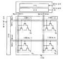
도 1은 본 발명의 일 형태인 반도체 장치의 일례를 나타내는 상면도 및 단면도이다.
도 2는 본 발명의 일 형태인 반도체 장치의 제작 공정의 일례를 도시하는 단면도이다.
도 3은 본 발명의 일 형태인 반도체 장치의 일례를 도시하는 단면도이다.
도 4는 본 발명의 일 형태인 반도체 장치의 제작 공정의 일례를 도시하는 단면도이다.
도 5는 본 발명의 일 형태인 반도체 장치의 일례를 도시하는 단면도이다.
도 6은 본 발명의 일 형태인 반도체 장치의 제작 공정의 일례를 도시하는 단면도이다.
도 7은 본 발명의 일 형태인 반도체 장치의 일례를 도시하는 단면도이다.
도 8은 본 발명의 일 형태인 반도체 장치의 일례를 도시하는 단면도이다.
도 9는 산화물 반도체 및 금속 재료의 밴드 구조를 설명하는 도면이다.
도 10은 본 발명의 일 형태를 도시하는 회로도의 일례이다.
도 11은 본 발명의 일 형태를 도시하는 회로도의 일례이다.
도 12는 본 발명의 일 형태를 도시하는 회로도의 일례이다.
도 13은 본 발명의 일 형태를 도시하는 회로도의 일례이다.
도 14는 CPU의 구체예를 도시하는 블록도 및 그의 일부의 회로도이다.1 is a top view and a cross-sectional view showing an example of a semiconductor device which is one embodiment of the present invention.
2 is a cross-sectional view showing an example of a manufacturing process of a semiconductor device which is one embodiment of the present invention.
3 is a cross-sectional view showing an example of a semiconductor device which is one embodiment of the present invention.
4 is a cross-sectional view showing an example of a manufacturing process of a semiconductor device which is one embodiment of the present invention.
5 is a cross-sectional view showing an example of a semiconductor device which is one embodiment of the present invention.
6 is a cross-sectional view showing an example of a manufacturing process of a semiconductor device which is one embodiment of the present invention.
7 is a cross-sectional view showing an example of a semiconductor device which is one embodiment of the present invention.
8 is a cross-sectional view showing an example of a semiconductor device which is one embodiment of the present invention.
9 is a view for explaining band structures of an oxide semiconductor and a metal material.
10 is an example of a circuit diagram showing an embodiment of the present invention.
11 is an example of a circuit diagram showing an embodiment of the present invention.
12 is an example of a circuit diagram showing an embodiment of the present invention.
13 is an example of a circuit diagram showing an embodiment of the present invention.
14 is a block diagram showing a specific example of the CPU and a circuit diagram of a part thereof.
본 발명의 실시 형태에 대해서 도면을 사용하여 상세하게 설명한다. 단, 본 발명은 이하의 설명에 한정되지 않고, 본 발명의 취지 및 그의 범위로부터 일탈하지 않고 그의 형태 및 상세 사항을 다양하게 변경할 수 있는 것은 당업자라면 용이하게 이해된다. 따라서, 본 발명은 이하에 나타내는 실시 형태의 기재 내용에 한정하여 해석되는 것이 아니다. 또한, 이하에 설명하는 본 발명의 구성에 있어서, 동일 부분 또는 동일 기능을 갖는 부분에는 동일한 부호를 서로 다른 도면 간에 공통되어서 사용하고, 그의 반복의 설명은 생략한다.BEST MODE FOR CARRYING OUT THE INVENTION Embodiments of the present invention will be described in detail with reference to the drawings. However, the present invention is not limited to the following description, and it is easily understood by those skilled in the art that various changes can be made in form and details without departing from the spirit and scope of the present invention. Therefore, the present invention is not construed as being limited to the description of the embodiments described below. In the following description of the present invention, the same reference numerals are used for the same parts or portions having the same functions, and description of their repetition is omitted.
또한, 본 명세서에서 설명하는 각 도면에 있어서, 각 구성의 크기, 막의 두께, 또는 영역은 명료화를 위하여 과장되어 있는 경우가 있다. 따라서, 반드시 그의 스케일에 한정되는 것은 아니다.In each of the drawings described in this specification, the size of each constitution, the thickness or the area of the film may be exaggerated for clarity. Therefore, it is not necessarily limited to his scale.
또한, 본 명세서에서 사용하는 제1, 제2, 제3 등의 용어는 구성 요소의 혼동을 피하기 위하여 붙인 것이며, 수적으로 한정하는 것이 아니다. 그로 인해, 예를 들어, 「제1」를 「제2」 또는 「제3」 등과 적절히 치환하여 설명할 수 있다.The terms of the first, second, third, etc. used in the present specification are added to avoid confusion of components, and are not limited to numerical values. Therefore, for example, " first " can be explained by appropriately substituting " second "
(실시 형태 1)(Embodiment 1)
본 실시 형태에서는 도 1 및 도 2를 사용하여, 이온 첨가되어 있지 않은 제1 산화물 반도체 영역으로 이루어지는 채널 영역을 갖는 톱 게이트 구조의 트랜지스터에 있어서, 채널 영역과 동일층에 형성되는 이온 첨가된 제2 산화물 반도체 영역에서 소스 영역 및 드레인 영역을 구성한 예를 설명한다.1 and 2, in the transistor of the top gate structure having a channel region composed of the first oxide semiconductor region which is not doped with ions, An example in which the source region and the drain region are formed in the oxide semiconductor region will be described.
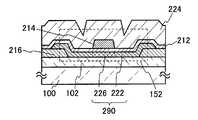
도 1은 톱 게이트 구조의 트랜지스터의 상면도 및 단면도이다. 여기서, 도 1의 (A)는 상면도이며, 도 1의 (B) 및 도 1의 (C)는 각각, 도 1의 (A)에 있어서의 A-B 단면 및 C-D 단면에 있어서의 단면도이다. 또한, 도 1의 (A)에서는 복잡해지지 않도록, 트랜지스터(151)의 구성 요소의 일부(예를 들어, 게이트 절연막(112), 층간 절연막(124) 등)을 생략하고 있다.1 is a top view and a cross-sectional view of a top gate structure transistor. 1 (A) is a top view, and FIGS. 1 (B) and 1 (C) are cross-sectional views taken along the line A-B and the line C-D in FIG. 1 (A), a part of the constituent elements of the transistor 151 (for example, the
도 1에 도시하는 트랜지스터(151)는 절연 표면 위의 제1 산화물 반도체 영역(126) 및 한 쌍의 제2 산화물 반도체 영역(122)을 포함하는 산화물 반도체막(190)과, 산화물 반도체막(190) 위의 게이트 절연막(112)과, 게이트 절연막(112) 위의 게이트 전극(114)과, 게이트 절연막(112) 및 게이트 전극(114)을 덮는 층간 절연막(124)과, 층간 절연막(124)에 형성된 콘택트 홀(130)에 있어서, 한 쌍의 제2 산화물 반도체 영역(122)과 접속된 배선(116)을 갖는 트랜지스터이다. 본 실시 형태에서는 절연 표면으로서 기판(100) 위에 하지 절연막(102)을 형성한 경우에 대하여 설명한다.The
여기서, 한 쌍의 제2 산화물 반도체 영역(122)은 트랜지스터(151)의 소스 영역 및 드레인 영역이 되고, 제1 산화물 반도체 영역(126)은 트랜지스터(151)의 채널 영역이 된다.Here, the pair of second
제1 산화물 반도체 영역(126) 및 한 쌍의 제2 산화물 반도체 영역(122)을 포함하는 산화물 반도체막(190)은 In, Ga, Sn 및 Zn 중에서 선택된 2종 이상의 원소를 포함하는 재료로 하면 된다. 예를 들어, 산화물 반도체막(190)은 In-Ga-Zn-O계 산화물 반도체로 한다.The
또한, 제1 산화물 반도체 영역(126)은 CAAC-OS이다.Also, the first
한 쌍의 제2 산화물 반도체 영역(122)은 비정질 영역이다. 또한, 제2 산화물 반도체 영역(122)은 수소 또는 희가스 중 임의의 1 이상의 원소가 포함되어 있고, 그의 농도는, 5×10¹⁸ atoms/cm3 이상 1×10²² atoms/cm3 이하인 것이 바람직하다.The pair of second
또한, 한 쌍의 제2 산화물 반도체 영역(122)은 도전율이 10 S/cm 이상 1000 S/cm 이하, 바람직하게는 100 S/cm 이상 1000 S/cm 이하로 한다. 도전율이 너무 낮으면 트랜지스터의 온 전류가 저하해 버린다. 또한, 도전율이 너무 높지 않도록 함으로써 한 쌍의 제2 산화물 반도체 영역(122)에서 발생하는 전계의 영향을 완화하여, 단채널 효과를 억제할 수 있다.The conductivity of the pair of second
층간 절연막(124)의 재료는, 예를 들어 산화실리콘, 산화질화실리콘, 질화산화실리콘, 질화실리콘, 산화알루미늄 등을 사용하면 되고, 적층 또는 단층으로 형성할 수 있다. 예를 들어, 열산화법, CVD법 또는 스퍼터링법 등으로 형성하면 된다. 바람직하게는, 층간 절연막(124)은 질화실리콘막 또는 질화산화실리콘막을 사용한다.The material of the
배선(116)은 후술하는 게이트 전극(114)과 동일한 구성으로 하면 된다.The
이러한 구조를 가짐으로써 게이트 전극(114)과 한 쌍의 제2 산화물 반도체 영역(122)과의 사이에 발생하는 기생 용량이 거의 없고, 트랜지스터를 미세화하고, 채널 길이를 축소한 경우에도 임계값의 변동을 저감할 수 있다. 또한, 한 쌍의 제2 산화물 반도체 영역(122)과 배선(116)의 콘택트 저항이 저감되어, 트랜지스터의 온 전류를 증대할 수 있다. 또한, 제1 산화물 반도체 영역(126) 내의 수소 농도가 저감되어, 트랜지스터의 전기 특성 및 신뢰성을 높일 수 있다.By virtue of such a structure, there is almost no parasitic capacitance generated between the
또한, 특별히 도시하지 않지만, 게이트 절연막(112)이 제1 산화물 반도체 영역(126) 위에만 형성되고, 한 쌍의 제2 산화물 반도체 영역(122)을 덮고 있지 않은 구조이어도 상관없다.Although not particularly shown, the structure may be such that the
<트랜지스터의 제조 방법의 일례>≪ Example of a method of manufacturing a transistor &
이어서, 도 1에 도시한 트랜지스터의 제조 방법에 대해서 도 2를 사용하여 설명한다.Next, a method of manufacturing the transistor shown in Fig. 1 will be described with reference to Fig.
우선, 도 2의 (A)에 도시한 바와 같이, 기판(100) 위에 하지 절연막(102)을 형성한다.First, as shown in Fig. 2A, a
기판(100)의 재질 등에 큰 제한은 없지만, 적어도 나중의 열처리에 견딜 수 있을 정도의 내열성을 갖고 있을 필요가 있다. 예를 들어, 유리 기판, 세라믹 기판, 석영 기판, 사파이어 기판 등을 사용해도 된다. 또한, 실리콘이나 탄화 실리콘 등의 단결정 반도체 기판, 다결정 반도체 기판, 실리콘 게르마늄, 질화갈륨 등의 화합물 반도체 기판, SOI 기판 등을 적용하는 것도 가능하고, 이들 기판 상에 반도체 소자가 형성된 것을 기판(100)으로서 사용해도 된다.There is no particular limitation on the material of the
또한, 기판(100)으로서 가요성 기판을 사용해도 된다. 가요성 기판 상에 트랜지스터를 형성하는 경우, 가요성 기판 상에 직접 트랜지스터를 제작해도 되고, 다른 기판에 트랜지스터를 제작한 후, 이것을 박리하고, 가요성 기판에 전치해도 된다. 또한, 트랜지스터를 박리하고, 가요성 기판에 전치하기 위해서는, 상기 다른 기판과 트랜지스터 사이에 박리층을 형성하면 된다.Further, a flexible substrate may be used as the
하지 절연막(102)은 산화실리콘막, 산화질화실리콘막, 질화산화실리콘막, 질화실리콘막 또는 산화알루미늄막의 단층 또는 적층으로 하면 된다.The underlying
여기서, 산화질화실리콘이란 그의 조성에 있어서, 질소보다 산소의 함유량이 많은 것을 나타내고, 예를 들어, 산소가 50 원자% 이상 70 원자% 이하, 질소가 0.5 원자% 이상 15 원자% 이하, 규소가 25 원자% 이상 35 원자% 이하, 수소가 0 원자% 이상 10 원자% 이하의 범위로 포함되는 것을 말한다. 또한, 질화산화실리콘이란 그의 조성에 있어서, 산소보다 질소의 함유량이 많은 것을 나타내고, 예를 들어, 산소가 5 원자% 이상 30 원자% 이하, 질소가 20 원자% 이상 55 원자% 이하, 규소가 25 원자% 이상 35 원자% 이하, 수소가 10 원자% 이상 25 원자% 이하의 범위로 포함되는 것을 말한다. 단, 상기 범위는 러더포드 후방 산란법(RBS: Rutherford Backscattering Spectrometry)이나, 수소 전방 산란법(HFS: Hydrogen Forward Scattering)을 사용하여 측정한 경우의 것이다. 또한, 구성 원소의 함유 비율은 그의 합계가 100 원자%를 초과하지 않는 값을 취한다.For example, oxygen is contained in an amount of 50 atomic% or more and 70 atomic% or less, nitrogen is contained in an amount of 0.5 atomic% or more and 15 atomic% or less, silicon is 25 To 35 atomic% or less, and hydrogen to 0 atomic% or more and 10 atomic% or less. For example, oxygen is contained in an amount of 5 atomic% or more and 30 atomic% or less, nitrogen is contained in an amount of 20 atomic% or more and 55 atomic% or less, silicon is 25 To 35 atomic% or less, and hydrogen to 10 atomic% or more and 25 atomic% or less. However, the range is measured by Rutherford Backscattering Spectrometry (RBS) or Hydrogen Forward Scattering (HFS). Further, the content ratio of the constituent elements takes a value such that the total thereof does not exceed 100 atomic%.
하지 절연막(102)은 열처리에 의해 산소 방출되는 막을 사용해도 된다.The underlying
「열처리에 의해 산소 방출되는」이란 TDS(Thermal Desorption Spectroscopy: 승온 탈리 가스 분광법) 분석에서, 산소 원자로 환산한 산소의 방출량이 1.0×10¹⁸ atoms/cm3 이상, 바람직하게는 3.0×10²⁰ atoms/cm3 이상인 것을 말한다.The term " oxygen released by heat treatment " means that in the case of TDS (Thermal Desorption Spectroscopy) analysis, the amount of released oxygen in terms of oxygen atoms is 1.0 x 10¹⁸ atoms / cm3 or more, preferably 3.0 x 10²⁰ atoms / cm <3 & gt ;.
여기서, TDS 분석에서, 산소 원자로 환산한 산소의 방출량의 측정 방법에 대해서 이하에 설명한다.Here, in the TDS analysis, a method of measuring the amount of released oxygen in terms of oxygen atoms will be described below.
TDS 분석했을 때의 기체의 방출량은 스펙트럼의 적분값에 비례한다. 이로 인해, 절연막의 스펙트럼의 적분값과, 표준 시료의 기준값에 대한 비에 의해 기체의 방출량을 계산할 수 있다. 표준 시료의 기준값이란 소정의 원자를 포함하는 시료의, 스펙트럼의 적분값에 대한 원자의 밀도의 비율이다.The emission of gas when analyzed by TDS is proportional to the integral of the spectrum. Therefore, the emission amount of the gas can be calculated by the ratio of the integral value of the spectrum of the insulating film to the reference value of the standard sample. The reference value of a standard sample is the ratio of the atomic density to the integral value of the spectrum of a sample containing a predetermined atom.
예를 들어, 표준 시료인 소정의 밀도의 수소를 포함하는 실리콘 웨이퍼의 TDS 분석 결과, 및 절연막의 TDS 분석 결과로부터, 절연막의 산소 분자의 방출량(NO2)은 수학식 1로 구할 수 있다. 여기서, TDS 분석에서 얻어지는 질량수 32로 검출되는 스펙트럼의 모두가 산소 분자에서 유래한다고 가정한다. 질량수 32의 것으로서 CH3OH가 있지만, 존재할 가능성이 낮은 것으로서 여기에서는 고려하지 않는다. 또한, 산소 원자의 동위체인 질량수 17의 산소 원자 및 질량수 18의 산소 원자를 포함하는 산소 분자에 대해서도, 자연계에 있어서의 존재 비율이 극미량이기 때문에 고려하지 않는다.For example, from the results of TDS analysis of a silicon wafer containing hydrogen of a predetermined density, which is a standard sample, and of TDS analysis of an insulating film, the emission amount (NO2 ) of oxygen molecules of the insulating film can be found by the following equation (1). Here, it is assumed that all of the spectra detected as the mass number 32 obtained from the TDS analysis comes from the oxygen molecule. Examples of the mass number 32 is CH3 OH, but, are not considered here as a low potential is present. In addition, regarding oxygen molecules containing an oxygen atom having a mass number of 17 and an oxygen atom having a mass number of 18, which are isotopes of oxygen atoms, the existence ratio in the natural world is negligible.

NH2는 표준 시료로부터 탈리된 수소 분자를 밀도로 환산한 값이다. SH2는 표준 시료를 TDS 분석했을 때의 스펙트럼의 적분값이다. 여기서, 표준 시료의 기준값을 NH2/SH2로 한다. SO2는 절연막을 TDS 분석했을 때의 스펙트럼의 적분값이다. α는 TDS 분석에 있어서의 스펙트럼 강도에 영향을 미치는 계수이다. 수학식 1의 상세 사항에 대해서는, 일본 특허 공개 평6-275697 공보를 참조한다. 또한, 상기 절연막의 산소의 방출량은 전자 과학 주식회사 제조의 승온 탈리 분석 장치 EMD-WA1000S/W를 사용하고, 표준 시료로서 1×10¹⁶ atoms/cm3의 수소 원자를 포함하는 실리콘 웨이퍼를 사용하여 측정하였다.NH2 is a value obtained by converting the hydrogen molecules desorbed from the standard sample to the density. SH2 is the integral value of the spectrum when TDS analysis of the standard sample is performed. Here, the reference value of the standard sample is NH2 / SH2 . SO2 is the integrated value of the spectrum when the insulating film is analyzed by TDS. α is a coefficient affecting the spectral strength in TDS analysis. Regarding the details of the formula (1), reference is made to Japanese Patent Application Laid-Open No. 6-275697. The amount of oxygen released from the insulating film was measured using a temperature-rising desorption analyzer EMD-WA1000S / W manufactured by Electronics Science Co., Ltd. and using a silicon wafer containing hydrogen atoms at 1 x 10¹⁶ atoms / cm3 as a standard sample Respectively.
또한, TDS 분석에 있어서, 산소의 일부는 산소 원자로서 검출된다. 산소 분자와 산소 원자의 비율은 산소 분자의 이온화율로부터 산출할 수 있다. 또한, 상술한 α는 산소 분자의 이온화율을 포함하기 때문에, 산소 분자의 방출량을 평가함으로써 산소 원자의 방출량에 대해서도 어림잡을 수 있다.Further, in the TDS analysis, a part of oxygen is detected as an oxygen atom. The ratio of oxygen molecules to oxygen atoms can be calculated from the ionization rate of oxygen molecules. In addition, since? Includes the ionization rate of oxygen molecules, it is also possible to estimate the amount of released oxygen atoms by evaluating the release amount of oxygen molecules.
또한, NO2는 산소 분자의 방출량이다. 절연막에 있어서는, 산소 원자로 환산했을 때의 산소의 방출량은 산소 분자의 방출량의 2배가 된다.In addition, NO2 is a discharge amount of the molecular oxygen. In the insulating film, the amount of oxygen released in terms of oxygen atoms is twice the amount of oxygen molecules released.
상기 구성에 있어서, 열처리에 의해 산소 방출되는 절연막은 산소가 과잉인 산화실리콘(SiOX(X>2))이어도 된다. 산소가 과잉인 산화실리콘(SiOX(X>2))이란 실리콘 원자수의 2배보다 많은 산소 원자를 단위 체적당에 포함하는 것이다. 단위 체적당의 실리콘 원자수 및 산소 원자수는 러더포드 후방 산란법에 의해 측정한 값이다.In the above structure, the insulating film that is oxygen-released by the heat treatment may be silicon oxide (SiOx (X > 2)) in which oxygen is excessive. The silicon oxide (SiOx (X > 2)) in which oxygen is excessively contained contains oxygen atoms in an amount more than twice the number of silicon atoms. The number of silicon atoms and the number of oxygen atoms per unit volume are values measured by the Rutherford back scattering method.
하지 절연막으로부터 산화물 반도체막에 산소가 공급됨으로써 하지 절연막 및 산화물 반도체막의 계면 준위를 저감할 수 있다. 이 결과, 트랜지스터의 동작 등에 기인하여 발생할 수 있는 전하 등이, 상술한 하지 절연막 및 산화물 반도체막의 계면에 포획되는 것을 억제할 수 있고, 전기 특성의 열화가 적은 트랜지스터를 얻을 수 있다.The interface level of the underlying insulating film and the oxide semiconductor film can be reduced by supplying oxygen from the underlying insulating film to the oxide semiconductor film. As a result, it is possible to suppress a charge or the like which may be caused due to the operation of the transistor or the like from being trapped at the interface between the grounding insulating film and the oxide semiconductor film, and to obtain a transistor with little deterioration in electrical characteristics.
또한, 산화물 반도체막의 산소 결손에 기인하여 전하가 발생하는 경우가 있다. 일반적으로 산화물 반도체막의 산소 결손은, 일부가 도너가 되어 캐리어인 전자를 발생한다. 이 결과, 트랜지스터의 임계값 전압이 마이너스 방향으로 시프트해 버린다. 이 경향은 백채널측에서 발생하는 산소 결손에 있어서 현저하다. 또한, 본 실시 형태에 있어서의 백채널이란 산화물 반도체막에 있어서 하지 절연막측의 계면 근방을 가리킨다. 하지 절연막으로부터 산화물 반도체막에 산소가 충분히 방출됨으로써 임계값 전압이 마이너스 방향으로 시프트하는 요인인, 산화물 반도체막의 산소 결손을 보충할 수 있다.Further, charge may be generated due to oxygen deficiency of the oxide semiconductor film. Generally, the oxygen deficiency of the oxide semiconductor film becomes a donor part, and electrons which are carriers are generated. As a result, the threshold voltage of the transistor shifts in the minus direction. This tendency is remarkable in oxygen defects occurring on the back channel side. The back channel in the present embodiment refers to the vicinity of the interface on the bottom insulating film side in the oxide semiconductor film. The oxygen deficiency of the oxide semiconductor film which is a factor that the threshold voltage is shifted in the minus direction by sufficiently releasing oxygen from the underlying insulating film into the oxide semiconductor film can be compensated.
즉, 산화물 반도체막에 산소 결손이 발생하면, 하지 절연막과 산화물 반도체막과의 계면에 있어서의 전하의 포획을 억제하는 것이 곤란해지는 바, 하지 절연막에 열처리에 의해 산소 방출되는 절연막을 형성함으로써 산화물 반도체막 및 하지 절연막의 계면 준위, 및 산화물 반도체막의 산소 결손을 저감하고, 산화물 반도체막 및 하지 절연막의 계면에 있어서의 전하 포획의 영향을 작게 할 수 있다.That is, when oxygen deficiency occurs in the oxide semiconductor film, it is difficult to suppress the trapping of charges at the interface between the base insulating film and the oxide semiconductor film. As a result, by forming an insulating film that releases oxygen to the base insulating film by heat treatment, The interface level of the film and the underlying insulating film and the oxygen vacancy in the oxide semiconductor film can be reduced and the influence of charge trapping at the interface between the oxide semiconductor film and the underlying insulating film can be reduced.
이어서, 하지 절연막(102) 위에 산화물 반도체막(140)을 형성한다.Then, an
산화물 반도체막(140)은 스퍼터링법에 의해, 두께 1 nm 이상 50 nm 이하의 산화물 반도체막을 성막하고, 상기 산화물 반도체막 위에 마스크를 형성한 후, 상기 마스크를 사용하여 산화물 반도체막을 선택적으로 에칭하여 형성된다.The
산화물 반도체막을 에칭하기 위한 마스크는 포토리소그래피 공정, 잉크젯법, 인쇄법 등을 적절히 사용할 수 있다. 또한, 산화물 반도체막의 에칭은 습식 에칭 또는 건식 에칭을 적절히 사용할 수 있다.As the mask for etching the oxide semiconductor film, a photolithography process, an inkjet process, a printing process, or the like can be suitably used. Further, the etching of the oxide semiconductor film can suitably use wet etching or dry etching.
여기서, 산화물 반도체막을 성막하는 스퍼터링 장치에 대해서 이하에 상세 사항을 설명한다.Hereinafter, the sputtering apparatus for forming the oxide semiconductor film will be described in detail.
산화물 반도체막을 성막하는 처리실은 누설률을 1×10⁻¹⁰ Pa·m3/초 이하로 하는 것이 바람직하고, 그것에 의해 스퍼터링법에 의해 성막할 때, 막 내로의 불순물의 혼입을 저감할 수 있다.The treatment chamber for forming the oxide semiconductor film preferably has a leakage rate of 1 x 10 <-10 > Pa <3 > / sec or less.
누설률을 낮추기 위해서는, 외부 누설뿐만아니라 내부 누설을 저감 할 필요가 있다. 외부 누설이란 미소한 구멍이나 밀봉 불량 등에 의해 진공계의 밖으로부터 기체가 유입되는 것이다. 내부 누설이란 진공계 내의 밸브 등의 구획으로부터의 누설이나 내부의 부재로부터의 방출 가스에 기인한다. 누설률을 1×10⁻¹⁰ Pa·m3/초 이하로 하기 위해서는, 외부 누설 및 내부 누설의 양면으로부터 대책을 마련할 필요가 있다.In order to lower the leakage rate, it is necessary to reduce the internal leakage as well as the external leakage. The external leakage means that the gas is introduced from the outside of the vacuum system due to a minute hole or poor sealing. Internal leakage is caused by leakage from a compartment of a valve or the like in a vacuum system or released gas from an internal member. In order to set the leak rate to 1 × 10⁻¹⁰ Pa · m3 / sec or less, countermeasures must be prepared from both external leakage and internal leakage.
외부 누설을 저감시키기 위해서는, 처리실의 개폐 부분은 메탈 가스킷으로 밀봉하면 된다. 메탈 가스킷은 불화철, 산화알루미늄, 또는 산화크롬에 의해 피복된 금속 재료를 사용하면 바람직하다. 메탈 가스킷은 O링과 비교하여 밀착성이 높아 외부 누설을 저감할 수 있다. 또한, 불화철, 산화알루미늄, 산화크롬 등의 부동태에 의해 피복된 금속 재료를 사용함으로써 메탈 가스킷으로부터 발생하는 수소를 포함하는 방출 가스가 억제되고, 내부 누설도 저감할 수 있다.In order to reduce the external leakage, the opening and closing portions of the processing chamber may be sealed with a metal gasket. The metal gasket is preferably made of a metal material coated with iron fluoride, aluminum oxide, or chromium oxide. Compared with O-rings, the metal gasket has high adhesion and can reduce external leakage. Further, by using a metal material coated with passivation such as iron fluoride, aluminum oxide, or chromium oxide, the release gas containing hydrogen generated from the metal gasket is suppressed, and the internal leakage can also be reduced.
처리실의 내벽을 구성하는 부재로서, 수소를 포함하는 방출 가스가 적은 알루미늄, 크롬, 티타늄, 지르코늄, 니켈 또는 바나듐을 사용한다. 또한, 전술한 재료를 철, 크롬 및 니켈 등을 포함하는 합금 재료에 피복하여 사용해도 된다. 철, 크롬 및 니켈 등을 포함하는 합금 재료는 강성이 있고, 열에 강하고, 또한 가공에 적합하다. 여기서, 표면적을 작게 하기 위하여 부재의 표면 요철을 연마 등에 의해 저감해 두면, 방출 가스를 저감할 수 있다. 또는, 전술한 성막 장치의 부재를 불화철, 산화알루미늄, 산화크롬 등의 부동태로 피복해도 된다.As the member constituting the inner wall of the treatment chamber, aluminum, chromium, titanium, zirconium, nickel, or vanadium, which has a low emission gas containing hydrogen, is used. Further, the above-described material may be used by being coated on an alloy material containing iron, chromium, nickel, or the like. Alloy materials including iron, chromium, nickel, and the like are rigid, resistant to heat, and suitable for processing. Here, if the surface irregularities of the member are reduced by polishing or the like in order to reduce the surface area, the emission gas can be reduced. Alternatively, the members of the above-described film forming apparatus may be coated with passivate such as iron fluoride, aluminum oxide, or chromium oxide.
또한, 스퍼터링 가스를 처리실에 도입하기 직전에 스퍼터링 가스의 정제기를 설치하는 것이 바람직하다. 이때, 정제기로부터 처리실까지의 배관의 길이를 5m 이하, 바람직하게는 1m 이하로 한다. 배관의 길이를 5m 이하 또는 1m 이하로 함으로써 배관으로부터의 방출 가스의 영향을 길이에 따라서 저감할 수 있다.It is also preferable that a purifier for sputtering gas be provided immediately before introducing the sputtering gas into the processing chamber. At this time, the length of the pipe from the purifier to the treatment chamber is set to 5 m or less, preferably 1 m or less. By reducing the length of the pipe to 5 m or less or 1 m or less, the influence of the discharged gas from the pipe can be reduced according to the length.
처리실의 배기는 드라이 펌프 등의 러핑 진공 펌프와, 스퍼터 이온 펌프, 터보 분자 펌프 및 크라이오 펌프 등의 고진공 펌프를 적절히 조합하여 행하면 된다. 터보 분자 펌프는 큰 크기의 분자의 배기가 우수한 한편, 수소나 물의 배기 능력이 낮다. 따라서, 물의 배기 능력이 높은 크라이오 펌프 및 수소의 배기 능력이 높은 스퍼터 이온 펌프를 조합하는 것이 유효하다.The exhaust of the treatment chamber may be performed by appropriately combining a roughing vacuum pump such as a dry pump and a high vacuum pump such as a sputter ion pump, a turbo molecular pump, and a cryo pump. The turbo molecular pump is excellent in exhausting molecules of large size, but also has a low ability to evacuate water or water. Therefore, it is effective to combine a cryopump having a high water discharging ability and a sputter ion pump having a high hydrogen discharging ability.
처리실의 내측에 존재하는 흡착물은 내벽에 흡착하고 있기 때문에 처리실의 압력에 영향을 미치지 않지만, 처리실을 배기했을 때의 가스 방출의 원인이 된다. 그러므로, 누설률과 배기 속도에 상관은 없지만, 배기 능력이 높은 펌프를 사용하여 처리실에 존재하는 흡착물을 가능한 한 탈리하여 미리 배기해 두는 것이 중요하다. 또한, 흡착물의 탈리를 촉진하기 위해서 처리실을 베이킹해도 된다. 베이킹함으로써 흡착물의 탈리 속도를 10배 정도 크게 할 수 있다. 베이킹은 100℃ 이상 450℃ 이하에서 행하면 된다. 이때, 불활성 가스를 도입하면서 흡착물의 제거를 행하면, 배기하기만 해서는 탈리하기 어려운 물 등의 탈리 속도를 더 빠르게 할 수 있다.Since the adsorbate existing inside the treatment chamber is adsorbed on the inner wall, it does not affect the pressure of the treatment chamber, but causes release of gas when the treatment chamber is evacuated. Therefore, although there is no relation to the leakage rate and the exhaust speed, it is important to exhaust the adsorbent present in the treatment chamber as much as possible by using a pump having a high exhausting ability and exhaust it in advance. Further, the treatment chamber may be baked to promote desorption of the adsorbed matter. By baking, the desorption rate of the adsorbate can be increased by about 10 times. The baking may be performed at a temperature of 100 ° C or more and 450 ° C or less. At this time, if the adsorbate is removed while introducing the inert gas, it is possible to accelerate the desorption rate of water or the like which is difficult to desorb only by exhausting.
스퍼터링법에 있어서, 플라즈마를 발생시키기 위한 전원 장치는 RF 전원 장치, AC 전원 장치, DC 전원 장치 등을 적절히 사용할 수 있다.In the sputtering method, an RF power source device, an AC power source device, a DC power source device, or the like can be suitably used as a power source device for generating plasma.
타깃으로서는, 아연을 포함하는 금속 산화물 타깃을 사용할 수 있다. 타깃으로 하여는, 4원계 금속 산화물인 In-Sn-Ga-Zn-O계 금속 산화물이나, 3원계 금속 산화물인 In-Ga-Zn-O계 금속 산화물, In-Sn-Zn-O계 금속 산화물, In-Al-Zn-O계 금속 산화물, Sn-Ga-Zn-O계 금속 산화물, Al-Ga-Zn-O계 금속 산화물, Sn-Al-Zn-O계 금속 산화물이나, 2원계 금속 산화물인 In-Zn-O계 금속 산화물, Sn-Zn-O계 금속 산화물 등의 타깃을 사용할 수 있다.As the target, a metal oxide target including zinc can be used. As the target, an In-Sn-Zn-O-based metal oxide which is a quaternary metal oxide, an In-Ga-Zn-O-based metal oxide which is a ternary metal oxide, an In- Al-Zn-O-based metal oxide, Sn-Al-Zn-O-based metal oxide, Sn-Ga-Zn-O-based metal oxide, Al- In-Zn-O-based metal oxide, Sn-Zn-O-based metal oxide, or the like can be used.
타깃의 일례로서, In, Ga, 및 Zn을 포함하는 금속 산화물 타깃을 In2O3:Ga2O3:ZnO=1:1:1[mol수 비율]의 조성비로 한다. 또한, In2O3:Ga2O3:ZnO=1:1:2[mol수 비율]의 조성비를 갖는 타깃, 또는 In2O3:Ga2O3:ZnO=1:1:4[mol수 비율]의 조성비를 갖는 타깃, In2O3:Ga2O3:ZnO=2:1:8[mol수 비율]의 조성비를 갖는 타깃을 사용할 수도 있다.As a target, a metal oxide target containing In, Ga, and Zn is set to a composition ratio of In2 O3 : Ga2 O3 : ZnO = 1: 1: 1 [molar ratio]. A target having a composition ratio of In2 O3 : Ga2 O3 : ZnO = 1: 1: 2 [molar ratio] or a target having a composition ratio of In2 O3 : Ga2 O3 : ZnO = 1: 1: 4 [mol Number ratio], and a target having a composition ratio of In2 O3 : Ga2 O3 : ZnO = 2: 1: 8 [number of moles] may be used.
또한, 스퍼터링 가스는, 희가스(대표적으로는 아르곤), 산소, 희가스 및 산소의 혼합 가스를 적절히 사용한다. 또한, 스퍼터링 가스에는 수소, 물, 수산기 또는 수소화물 등의 불순물이 제거된 고순도 가스를 사용하는 것이 바람직하다.As the sputtering gas, a mixed gas of rare gas (typically argon), oxygen, rare gas and oxygen is suitably used. In addition, it is preferable to use a high-purity gas from which impurities such as hydrogen, water, hydroxyl, or hydride are removed as the sputtering gas.
또한, 성막 시의 기판 온도는 150℃ 이상 450℃ 이하, 바람직하게는 200℃ 이상 350℃ 이하이다. 150℃ 이상 450℃ 이하, 바람직하게는 200℃ 이상 350℃ 이하에 기판을 열처리하면서 성막을 함으로써 막 내로의 수분(수소를 포함함) 등의 혼입을 방지할 수 있다. 또한, 결정을 포함하는 산화물 반도체막인 CAAC-OS막을 형성할 수 있다.The substrate temperature at the time of film formation is 150 占 폚 or higher and 450 占 폚 or lower, preferably 200 占 폚 or higher and 350 占 폚 or lower. It is possible to prevent moisture (including hydrogen) and the like from being mixed into the film by performing film formation while the substrate is heat-treated at 150 ° C or more and 450 ° C or less, preferably 200 ° C or more and 350 ° C or less. Further, a CAAC-OS film which is an oxide semiconductor film containing crystals can be formed.
또한, 산화물 반도체막 성막 후에, 기판(100)에 열처리를 실시하고, 산화물 반도체막으로부터 수소를 방출시킴과 함께, 하지 절연막(102)에 포함되는 산소의 일부를, 산화물 반도체막과, 하지 절연막(102)에 있어서의 산화물 반도체막의 계면 근방으로 확산시키는 것이 바람직하다. 또한, 상기 열처리를 행함으로써 보다 결정성이 높은 CAAC-OS막을 형성할 수 있다.After the oxide semiconductor film is formed, the
상기 열처리의 온도는 산화물 반도체막으로부터 수소를 방출시킴과 함께, 하지 절연막(102)에 포함되는 산소의 일부를 방출시키고, 나아가 산화물 반도체막으로 확산시키는 온도가 바람직하고, 대표적으로는, 200℃ 이상 기판(100)의 변형점 미만, 바람직하게는 250℃ 이상 450℃ 이하로 한다.The temperature for the heat treatment is preferably a temperature at which hydrogen is emitted from the oxide semiconductor film and a part of oxygen contained in the
또한 상기 열처리는 RTA(Rapid Thermal Anneal) 장치를 사용할 수 있다. RTA 장치를 사용함으로써 단시간에 한하여 기판의 변형점 이상의 온도에서 열처리를 행할 수 있다. 그로 인해, 비정질 영역보다 결정 영역의 비율이 많은 산화물 반도체막을 형성하기 위한 시간을 단축할 수 있다.The heat treatment may be performed using a RTA (Rapid Thermal Anneal) apparatus. By using the RTA apparatus, the heat treatment can be performed at a temperature higher than the strain point of the substrate within a short time. As a result, the time for forming the oxide semiconductor film having a larger crystal region ratio than the amorphous region can be shortened.
열처리는 불활성 가스 분위기에서 행할 수 있고, 대표적으로는, 헬륨, 네온, 아르곤, 크세논, 크립톤 등의 희가스, 또는 질소 분위기에서 행하는 것이 바람직하다. 또한, 산소 분위기 및 감압 분위기에서 행해도 된다. 처리 시간은 3분 내지 24시간으로 한다. 처리 시간을 길게 할수록 비정질 영역보다 결정 영역의 비율이 많은 산화물 반도체막을 형성할 수 있지만, 24시간을 초과하는 열처리는 생산성의 저하를 초래하기 때문에 바람직하지 않다.The heat treatment can be performed in an inert gas atmosphere. Typically, the heat treatment is preferably performed in a rare gas such as helium, neon, argon, xenon, krypton, or a nitrogen atmosphere. It may also be performed in an oxygen atmosphere and a reduced pressure atmosphere. The treatment time is 3 minutes to 24 hours. An oxide semiconductor film having a larger crystal region ratio than the amorphous region can be formed with a longer processing time, but a heat treatment exceeding 24 hours is not preferable because it causes a decrease in productivity.
또한, 상기 CAAC-OS막의 제조 방법은, 본 실시 형태에 나타내는 형성 방법에 한정되는 것은 아니다.The method of producing the CAAC-OS film is not limited to the forming method described in this embodiment.
이와 같이, 산화물 반도체막의 성막 공정에 있어서, 처리실의 압력, 처리실의 누설률 등에 있어서, 불순물의 혼입을 최대한 억제함으로써 산화물 절연막 및 산화물 반도체막에 포함되는 수소 등 불순물의 혼입을 저감할 수 있다. 또한, 산화물 절연막으로부터 산화물 반도체막에의 수소 등 불순물의 확산을 저감할 수 있다. 산화물 반도체에 포함되는 수소는 금속 원자와 결합하는 산소와 반응하여 물이 됨과 동시에, 산소가 탈리한 격자(또는 산소가 탈리한 부분)에는 결함이 형성되어 버린다.As described above, mixing of impurities such as hydrogen contained in the oxide insulating film and the oxide semiconductor film can be reduced by suppressing the mixing of impurities to the maximum in the process chamber forming pressure, the leakage rate of the processing chamber, and the like in the process of forming the oxide semiconductor film. In addition, diffusion of impurities such as hydrogen from the oxide insulating film to the oxide semiconductor film can be reduced. Hydrogen contained in the oxide semiconductor reacts with oxygen bonded to the metal atoms to form water, and defects are formed in the lattice in which oxygen has been eliminated (or in the portion where oxygen is eliminated).
이로 인해, 산화물 반도체막의 성막 공정에 있어서, 불순물을 극도로 저감시킴으로써 산화물 반도체막의 결함을 저감하는 것이 가능하다. 이러한 점에서, 불순물을 가능한 한 제거하고, 고순도화시킨 CAAC-OS를 채널 영역으로 함으로써 트랜지스터에 대한 광 조사나 BT 시험 전후에서의 임계값 전압의 변화량이 적기 때문에 안정된 전기적 특성을 가질 수 있다.Therefore, it is possible to reduce the defects of the oxide semiconductor film by extremely reducing the impurities in the process of forming the oxide semiconductor film. In this respect, since the impurity is removed as much as possible and the high-purity CAAC-OS is used as the channel region, stable electrical characteristics can be obtained because the amount of change in the threshold voltage before and after the light irradiation or BT test for the transistor is small.
또한, 산화물 반도체막에 사용하는 것이 가능한 금속 산화물은 밴드 갭이 2 eV 이상, 바람직하게는 2.5 eV 이상, 보다 바람직하게는 3 eV 이상이다. 이와 같이, 밴드 갭이 넓은 금속 산화물을 사용함으로써 트랜지스터의 오프 전류를 저감할 수 있다.The metal oxide that can be used for the oxide semiconductor film has a band gap of 2 eV or more, preferably 2.5 eV or more, and more preferably 3 eV or more. As described above, by using a metal oxide having a wide band gap, the off current of the transistor can be reduced.
이어서, 산화물 반도체막(140) 위에 게이트 절연막(112), 게이트 전극(114)을 형성한다. 게이트 전극(114)은 도전막을 성막하고, 상기 도전막 위에 마스크를 형성한 후, 상기 마스크를 사용하여 도전막을 선택적으로 에칭하여 형성된다.Then, a
게이트 절연막(112)은 예를 들어 산화실리콘, 산화질화실리콘, 질화산화실리콘, 질화실리콘, 산화알루미늄, 산화하프늄 또는 산화갈륨 등을 사용하면 되고, 적층 또는 단층으로 형성한다. 예를 들어, 열산화법, CVD법, 스퍼터링법 등으로 형성하면 된다. 게이트 절연막(112)은 열처리에 의해 산소 방출되는 막을 사용해도 된다. 게이트 절연막(112)에 열처리에 의해 산소 방출되는 막을 사용함으로써 산화물 반도체에 발생하는 산소 결손을 수복할 수 있고, 트랜지스터의 전기 특성의 열화를 억제할 수 있다.The
또한, 게이트 절연막(112)로서, 하프늄실리케이트(HfSiOx), 질소가 첨가된 하프늄실리케이트(HfSixOyNz), 질소가 첨가된 하프늄알루미네이트(HfAlxOyNz), 산화하프늄, 산화이트륨 등의 high-k 재료를 사용함으로써 게이트 누설을 저감할 수 있다. 나아가, high-k 재료와, 산화실리콘, 산화질화실리콘, 질화실리콘, 질화산화실리콘, 산화알루미늄, 산화질화알루미늄, 또는 산화갈륨 중 어느 하나 이상과의 적층 구조로 할 수 있다. 게이트 절연막(112)의 두께는 1 nm 이상 300 nm 이하, 보다 바람직하게는 5 nm 이상 50 nm 이하로 하면 된다.As the
게이트 전극(114)은 알루미늄, 크롬, 구리, 탄탈, 티타늄, 몰리브덴, 텅스텐으로 선택된 금속 원소, 또는 상술한 금속 원소를 성분으로 하는 합금이나, 상술한 금속 원소를 조합한 합금 등을 사용하여 형성할 수 있다. 또한, 망간, 지르코늄 중 어느 하나 또는 복수 중에서 선택된 금속 원소를 사용해도 된다. 또한, 게이트 전극(114)은 단층 구조나, 2층 이상의 적층 구조로 해도 된다. 예를 들어, 실리콘을 포함하는 알루미늄막의 단층 구조, 알루미늄막 위에 티타늄막을 적층하는 2층 구조, 질화티타늄막 위에 티타늄막을 적층하는 2층 구조, 질화티타늄막 위에 텅스텐막을 적층하는 2층 구조, 질화탄탈막 위에 텅스텐막을 적층하는 2층 구조, 티타늄막과, 그 티타늄막 위에 알루미늄막을 적층하고, 또한 그 위에 티타늄막을 형성하는 3층 구조 등이 있다.The
또한, 게이트 전극(114)은 인듐 주석 산화물, 산화텅스텐을 포함하는 인듐 산화물, 산화텅스텐을 포함하는 인듐 아연 산화물, 산화티타늄을 포함하는 인듐 산화물, 산화티타늄을 포함하는 인듐 주석 산화물, 인듐 아연 산화물, 산화규소를 첨가한 인듐 주석 산화물 등의 투광성을 갖는 도전성 재료를 적용할 수도 있다. 또한, 상기 투광성을 갖는 도전성 재료와, 상기 금속 원소의 적층 구조로 할 수도 있다.The
또한, 게이트 전극(114)과 게이트 절연막(112) 사이에 게이트 절연막(112)에 접하는 재료층으로서 질소를 포함하는 In-Ga-Zn-O막이나, 질소를 포함하는 In-Sn-O막이나, 질소를 포함하는 In-Ga-O막이나, 질소를 포함하는 In-Zn-O막이나, 질소를 포함하는 Sn-O막이나, 질소를 포함하는 In-O막이나, 금속 질화막(InN, ZnN 등)을 형성하는 것이 바람직하다. 이들 막은 5 eV, 바람직하게는 5.5 eV 이상의 일함수를 갖고, 트랜지스터의 전기 특성의 임계값 전압을 플러스로 할 수 있어, 소위 노멀리 오프의 스위칭 소자를 실현할 수 있다. 예를 들어, 질소를 포함하는 In-Ga-Zn-O막을 사용하는 경우, 적어도 산화물 반도체막(140)보다 높은 질소 농도, 구체적으로는 7 원자% 이상의 In-Ga-Zn-O막을 사용한다.An In-Ga-Zn-O film containing nitrogen or an In-Sn-O film containing nitrogen as a material layer in contact with the
이어서, 도 2의 (B)에 도시한 바와 같이, 산화물 반도체막(140)에 이온(150)을 첨가하는 처리를 행한다.Next, as shown in FIG. 2B, a process of adding
산화물 반도체막(140)에 이온(150)을 첨가하는 방법으로서 이온 도핑법 또는 이온 주입법을 사용할 수 있다. 또한, 첨가하는 이온(150)로서는, 산화물 반도체막을 덮고, 절연막 등이 형성되어 있는 상태에서의 이온 첨가에 있어서는, 수소 또는 희가스 중에서 선택할 수 있다. 또한, 산화물 반도체막이 노출되어 있는 상태에서의 이온 첨가에 있어서는 수소를 사용할 수 있다. 도 2의 (B)에 도시한 바와 같이 이온(150)의 첨가를 행함으로써 게이트 전극(114)이 마스크가 되기 때문에, 자기정합적으로 이온(150)이 첨가되는 영역인 제2 산화물 반도체 영역(122) 및 이온이 첨가되지 않은 영역인 제1 산화물 반도체 영역(126)이 형성된다(도 2의 (C)참조.).As a method of adding the
또한, 이온(150)이 첨가된 제2 산화물 반도체 영역(122)은 이온 첨가의 데미지에 의해 결정성이 저감함으로써 비정질 영역이 된다. 또한, 이온의 첨가량 등의 첨가 조건을 조절함으로써 산화물 반도체에의 데미지량을 저감시킴으로써 완전한 비정질 영역이 되지 않도록 형성할 수도 있다. 그 경우, 제2 산화물 반도체 영역(122)은 적어도 제1 산화물 반도체 영역(126)보다 비정질 영역의 비율이 큰 영역이 된다.In addition, the second
또한, 상기 이온(150)의 첨가는 이온 도핑법 또는 이온 주입법 등을 이용한 주입 이외의 방법으로도 행할 수 있다. 예를 들어, 첨가하는 원소를 포함하는 가스 분위기에서 플라즈마를 발생시켜서 피첨가물에 대하여 플라즈마 처리를 행함으로써 이온을 첨가할 수 있다. 상기 플라즈마를 발생시키는 장치로서는 건식 에칭 장치나 플라즈마 CVD 장치, 고밀도 플라즈마 CVD 장치 등을 사용할 수 있다.The
또한, 상기 이온(150)을 첨가한 후에 열처리를 행해도 된다. 상기 열처리는 제2 산화물 반도체 영역(122)이 결정화하지 않는 온도가 바람직하다.Further, the heat treatment may be performed after the
이어서, 도 2의 (D)에 도시한 바와 같이, 게이트 절연막(112) 및 게이트 전극(114) 위에 층간 절연막(124)을 형성하고, 상기 층간 절연막(124)에 콘택트 홀(130)을 형성한다. 상기 콘택트 홀(130)에 있어서, 한 쌍의 제2 산화물 반도체 영역(122)과 접속하는 배선(116)을 형성한다.2 (D), an
층간 절연막(124)의 재료는, 산화실리콘, 산화질화실리콘, 질화산화실리콘, 질화실리콘, 산화알루미늄, 질화알루미늄을 단층 또는 적층시켜서 사용할 수 있고, 스퍼터링법, CVD법 등에서 성막하면 된다. 이때, 열처리에 의해 산소를 방출하기 어려운 재료를 사용하는 것이 바람직하다. 이것은, 한 쌍의 제2 산화물 반도체 영역(122)의 도전율을 저하시키지 않기 위해서이다. 구체적으로는, CVD법에 의해, 실란 가스를 주재료로 하고, 산화질소 가스, 질소 가스, 수소 가스 및 희가스로부터 적절한 원료 가스를 혼합하여 성막하면 된다. 또한, 기판 온도를 300℃ 이상 550℃ 이하로 하면 된다. CVD법을 사용함으로써 열처리에 의해 산소를 방출하기 어려운 재료로 할 수 있다. 또한, 실란 가스를 주재료로 함으로써 막 내에 수소가 잔류하고, 상기 수소가 확산함으로써 한 쌍의 제2 산화물 반도체 영역(122)의 도전율을 더 높일 수 있다. 층간 절연막(124) 중의 수소 농도는 0.1 원자% 이상 25 원자% 이하로 하면 된다.The material of the
배선(116)의 재료는 게이트 전극(114)과 동일한 구성으로 하면 된다.The
이상과 같은 공정에 의해 트랜지스터를 미세화하고, 채널 길이를 축소한 때에도 전기 특성이 양호하고, 또한 신뢰성이 높은 산화물 반도체를 사용한 트랜지스터를 제작할 수 있다.A transistor using an oxide semiconductor having good electric characteristics and high reliability can be manufactured even when the transistor is miniaturized and the channel length is reduced by the above process.
본 실시 형태는 다른 실시 형태와 적절히 조합할 수 있다.This embodiment can be combined with other embodiments as appropriate.
(실시 형태 2)(Embodiment 2)
본 실시 형태에서는 실시 형태 1에서 나타낸 트랜지스터와 상이한 트랜지스터의 예에 대하여 도 3 및 도 4를 사용하여 설명한다.In the present embodiment, an example of a transistor different from the transistor shown in the first embodiment will be described with reference to Figs. 3 and 4. Fig.
도 3에 도시하는 트랜지스터(152)는 기판(100) 위의 하지 절연막(102)과, 하지 절연막(102) 위의 소스 전극 및 드레인 전극(216)과, 하지 절연막(102) 위의 제1 산화물 반도체 영역(226), 소스 전극 및 드레인 전극(216)과 접속된 한 쌍의 제2 산화물 반도체 영역(222)을 포함하는 산화물 반도체막(290)과, 산화물 반도체막(290) 위의 게이트 절연막(212)과, 게이트 절연막(212) 위의 게이트 전극(214)과, 게이트 절연막(212) 및 게이트 전극(214) 위의 층간 절연막(224)을 갖는 트랜지스터이다.The
트랜지스터의 채널 길이는 한 쌍의 제2 산화물 반도체 영역(222)의 간격으로 정해진다. 채널 길이와 게이트 전극(214)의 폭이 일치하는 경우, 한 쌍의 제2 산화물 반도체 영역(222)과 게이트 전극(214)의 겹침이 없어지기 때문에 바람직한데, 채널 길이와 게이트 전극(214)의 폭이 일치하지 않아도 상관없다. 예를 들어, 채널 길이 보다 게이트 전극(214)의 폭이 좁을 경우, 전계의 집중이 완화되는 효과에 의해 단채널 효과를 저감할 수 있다.The channel length of the transistor is determined by the interval of the pair of second
<트랜지스터의 제조 방법의 일례>≪ Example of a method of manufacturing a transistor &
이어서, 도 3에 도시한 트랜지스터의 제조 방법에 대해서 도 4를 사용하여 설명한다.Next, a method of manufacturing the transistor shown in Fig. 3 will be described with reference to Fig.
도 4의 (A)에 도시한 바와 같이, 기판(100) 위에 하지 절연막(102)을 형성한다.As shown in Fig. 4 (A), the
이어서, 하지 절연막(102) 위에 소스 전극 및 드레인 전극(216)을 형성하고, 하지 절연막(102) 및 소스 전극 및 드레인 전극(216) 위에 산화물 반도체막(240)을 형성한다. 산화물 반도체막(240)은 실시 형태 1의 산화물 반도체막(140)과 마찬가지로 형성할 수 있다.A source electrode and a
이어서, 소스 전극 및 드레인 전극(216) 및 산화물 반도체막(240)을 덮는 게이트 절연막(212)을 형성하고, 게이트 절연막(212) 위에 게이트 전극(214)을 형성한다.A
이어서, 도 4의 (B)에 도시한 바와 같이, 산화물 반도체막(240)에 이온(150)을 첨가하는 처리를 행한다. 이온(150)의 첨가는 실시 형태 1과 동일한 처리를 행할 수 있다. 게이트 전극(214)을 마스크로 하여 이온(150)을 첨가함으로써 자기정합적으로 이온(150)이 첨가된 제2 산화물 반도체 영역(222) 및 이온(150)이 첨가되지 않은 제1 산화물 반도체 영역(226)을 형성할 수 있다(도 4의 (C)참조.).Then, as shown in FIG. 4B, the
또한, 상기 이온(150)을 첨가한 후에 열처리를 행해도 된다. 상기 열처리는 제2 산화물 반도체 영역(222)이 결정화하지 않는 온도가 바람직하다.Further, the heat treatment may be performed after the
이어서, 도 4의 (D)에 도시한 바와 같이, 게이트 절연막(212) 및 게이트 전극(214) 위에 층간 절연막(224)을 형성한다. 또한, 특별히 도시하지 않지만, 층간 절연막(224)에 콘택트 홀을 형성하고, 상기 콘택트 홀에 있어서, 소스 전극 및 드레인 전극(216)과 접속하는 배선을 형성해도 된다.4D, an
이상과 같은 공정에 의해, 트랜지스터를 미세화하고, 채널 길이를 축소한 때에도 전기 특성이 양호하고, 또한 신뢰성이 높은 산화물 반도체를 사용한 트랜지스터를 제작할 수 있다.By the above-described process, a transistor using an oxide semiconductor having good electric characteristics and high reliability can be manufactured even when the transistor is miniaturized and the channel length is reduced.
본 실시 형태는 다른 실시 형태와 적절히 조합할 수 있다.This embodiment can be combined with other embodiments as appropriate.
(실시 형태 3)(Embodiment 3)
본 실시 형태에서는 실시 형태 1 및 실시 형태 2에서 나타낸 트랜지스터와 다른 트랜지스터의 예에 대하여 도 5 및 도 6을 사용하여 설명한다.In this embodiment, examples of transistors different from those described in the first and second embodiments will be described with reference to Figs. 5 and 6. Fig.
도 5에 도시하는 트랜지스터(153)은 절연 표면을 갖는 기판(100)과, 기판(100) 위의 게이트 전극(314)과, 게이트 전극(314) 위의 게이트 절연막(312)과, 게이트 절연막(312)을 개재하여 게이트 전극(314) 위에 형성된 제1 산화물 반도체 영역(326) 및 한 쌍의 제2 산화물 반도체 영역(322)을 포함하는 산화물 반도체막(390)과, 제1 산화물 반도체 영역(326) 위에 중첩하여 형성된 절연막(319)과, 한 쌍의 제2 산화물 반도체 영역(322)과 접속된 소스 전극 및 드레인 전극(316)과, 절연막(319) 및 소스 전극 및 드레인 전극(316) 위의 층간 절연막(324)을 갖는 트랜지스터이다. 또한, 기판(100) 위에 하지 절연막(102)을 갖는 구조로 해도 상관없다.5 includes a
트랜지스터의 채널 길이는 한 쌍의 제2 산화물 반도체 영역(322)의 간격으로 정해진다. 채널 길이와 게이트 전극(314)의 폭이 일치하는 경우, 한 쌍의 제2 산화물 반도체 영역(322)과 게이트 전극(314)과의 겹침이 없어지기 때문에 바람직한데, 채널 길이와 게이트 전극(314)의 폭이 일치하지 않아도 상관없다. 예를 들어, 채널 길이 보다 게이트 전극(314)의 폭이 좁을 경우, 전계의 집중이 완화되는 효과에 의해 단채널 효과를 저감할 수 있다.The channel length of the transistor is determined by the interval of the pair of second
<트랜지스터의 제조 방법의 일례>≪ Example of a method of manufacturing a transistor &
이어서, 도 5에 도시한 트랜지스터의 제조 방법에 대해서 도 6을 사용하여 설명한다.Next, a method of manufacturing the transistor shown in Fig. 5 will be described with reference to Fig.
도 6의 (A)에 도시한 바와 같이, 기판(100) 위에 하지 절연막(102)을 형성한다.6A, the
이어서, 하지 절연막(102) 위에 게이트 전극(314)을 형성하고, 게이트 전극(314)을 덮는 게이트 절연막(312)을 형성한다.Next, a
이어서, 게이트 절연막(312) 위에 산화물 반도체막(340)을 형성한다. 산화물 반도체막(340)은 실시 형태 1의 산화물 반도체막(140)과 마찬가지로 형성할 수 있다. 이어서, 산화물 반도체막(340) 위에 게이트 전극(314)과 중첩하는 절연막(319)을 형성한다.Then, an
이어서, 도 6의 (B)에 도시한 바와 같이, 산화물 반도체막(340)에 이온(150)을 첨가하는 처리를 행한다. 이온(150)에는 수소를 사용할 수 있다. 절연막(319)을 마스크로 하여 이온(150)을 첨가함으로써 자기정합적으로 이온(150)이 첨가된 제2 산화물 반도체 영역(322) 및 이온(150)이 첨가되지 않은 제1 산화물 반도체 영역(326)을 형성할 수 있다. 이어서, 제2 산화물 반도체 영역(322) 위에 소스 전극 및 드레인 전극(316)을 형성한다(도 6의 (C)참조.).Then, as shown in Fig. 6B, the
또한, 상기 이온(150)의 첨가는 이온 도핑법 또는 이온 주입법 등을 이용한 주입 이외의 방법으로도 행할 수 있다. 예를 들어, 첨가하는 원소를 포함하는 가스 분위기에서 플라즈마를 발생시켜서 피첨가물에 대하여 플라즈마 처리를 행함으로써 이온을 첨가할 수 있다. 상기 플라즈마를 발생시키는 장치로서는 건식 에칭 장치나 플라즈마 CVD 장치, 고밀도 플라즈마 CVD 장치 등을 사용할 수 있다.The
또한, 상기 이온(150)을 첨가한 후에 열처리를 행해도 된다. 상기 열처리는 제2 산화물 반도체 영역(322)이 결정화하지 않는 온도가 바람직하다.Further, the heat treatment may be performed after the
이어서, 도 6의 (D)에 도시한 바와 같이, 절연막(319), 제2 산화물 반도체 영역(322), 소스 전극 및 드레인 전극(316) 위에 층간 절연막(324)을 형성한다. 또한, 특별히 도시하지 않지만, 층간 절연막(324)에 콘택트 홀을 형성하고, 상기 콘택트 홀에 있어서, 소스 전극 및 드레인 전극(316)과 접속하는 배선을 형성해도 된다.6D, an
이상과 같은 공정에 의해, 트랜지스터를 미세화하고, 채널 길이를 축소한 때에도 전기 특성이 양호하고, 또한 신뢰성이 높은 산화물 반도체를 사용한 트랜지스터를 제작할 수 있다.By the above-described process, a transistor using an oxide semiconductor having good electric characteristics and high reliability can be manufactured even when the transistor is miniaturized and the channel length is reduced.
본 실시 형태는 다른 실시 형태와 적절히 조합할 수 있다.This embodiment can be combined with other embodiments as appropriate.
(실시 형태 4)(Fourth Embodiment)
본 실시 형태에서는 도 7을 사용하여 이온 첨가한 산화물 반도체를 사용한 저항 소자에 대하여 설명한다.In this embodiment, a resistance element using an oxide semiconductor doped with ions is described with reference to FIG.
도 7의 (A)는 절연 표면을 갖는 기판(100)과, 기판(100) 위에 형성되는 이온 첨가한 산화물 반도체막(401)을 저항으로 하고, 상기 산화물 반도체막(401)과 접하여 도전막(403)을 형성함으로써 형성한 저항 소자(410)을 나타내고 있다. 이온 첨가한 산화물 반도체막(401)은 실시 형태 2에서 나타낸 제2 산화물 반도체 영역(222)과 마찬가지로 형성할 수 있다. 또한, 도전막(403)은 소스 전극 및 드레인 전극(216)과 마찬가지의 재료로 형성할 수 있다. 또한, 본 실시 형태에서는 기판(100) 위에 하지 절연막(102)이 형성되어 있다.7A shows a structure in which a
도 7의 (B)는 절연 표면을 갖는 기판(100)과, 기판(100) 위에 형성되는 이온 첨가한 산화물 반도체막(421)을 저항으로 하고, 상기 산화물 반도체막(421)과 접하여 절연막(425)이 형성되어 있고, 상기 절연막(425)과, 상기 산화물 반도체막(421)의 일부가 접하여 도전막(423)을 형성함으로써 형성한 저항 소자(420)를 나타내고 있다. 이온 첨가한 산화물 반도체막(421)은 실시 형태 2에서 나타낸 제2 산화물 반도체 영역(222)과 마찬가지로 형성할 수 있다. 또한, 절연막(425)은 게이트 절연막(212)과 마찬가지의 재료로 형성할 수 있다. 또한, 도전막(423)은 소스 전극 및 드레인 전극(216)과 마찬가지의 재료로 형성할 수 있다. 이와 같이 하여 저항 소자(420)를 형성함으로써 저항 소자에 있어서의 도전막 간의 거리를 일정하게 할 수 있고, 저항 소자의 저항값을 보다 정밀도가 좋은 것으로 할 수 있다. 또한, 본 실시 형태에서는 기판(100) 위에 하지 절연막(102)이 형성되어 있다.7B shows a structure in which a
(실시 형태 5)(Embodiment 5)
본 실시 형태에서는 CAAC-OS막인 산화물 반도체막의 형성 방법에 대해서 실시 형태 1 내지 실시 형태 4에서 사용한 이외의 방법에 대해서 이하에 설명한다.In the present embodiment, a method for forming an oxide semiconductor film which is a CAAC-OS film will be described below in addition to the methods used in the first to fourth embodiments.
우선, 기판 상의 절연막에 접하는 제1 산화물 반도체막을 형성한다. 제1 산화물 반도체막은 1 원자층 이상 10 nm 이하, 바람직하게는 2 nm 이상 5 nm 이하로 한다.First, a first oxide semiconductor film in contact with an insulating film on a substrate is formed. The thickness of the first oxide semiconductor film is not less than 1 atomic layer and not more than 10 nm, preferably not less than 2 nm and not more than 5 nm.
제1 산화물 반도체막의 형성 시, 기판 온도를 150℃ 이상 450℃ 이하, 바람직하게는 200℃ 이상 350℃ 이하로 하는 것이 바람직하다. 그에 의해, 형성한 제1 산화물 반도체막 내에 포함되는 수분(수소를 포함함) 등의 불순물의 혼입을 저감시킬 수 있다. 또한, 제1 산화물 반도체막의 결정성을 향상시킬 수 있고, CAAC-OS막인 산화물 반도체막을 형성할 수 있다.At the time of forming the first oxide semiconductor film, the substrate temperature is preferably 150 占 폚 or higher and 450 占 폚 or lower, preferably 200 占 폚 or higher and 350 占 폚 or lower. Thereby, impurities such as moisture (including hydrogen) contained in the formed first oxide semiconductor film can be reduced. Further, the crystallinity of the first oxide semiconductor film can be improved, and an oxide semiconductor film which is a CAAC-OS film can be formed.
이어서, 제1 산화물 반도체막 형성 후, 제1 열처리를 행해도 된다. 상기 제1 열처리에 의해, 제1 산화물 반도체막으로부터 수분(수소 포함함)을 탈리시킬 수 있고, 또한 결정성도 향상시킬 수 있다. 상기 제1 열처리를 행함으로써 결정성이 높은 CAAC-OS막을 형성할 수 있다. 또한, 상기 제1 열처리는 200℃ 이상 기판의 변형점 미만, 바람직하게는 250℃ 이상 450℃ 이하로 한다.Then, after the first oxide semiconductor film is formed, the first heat treatment may be performed. By the first heat treatment, moisture (including hydrogen) can be desorbed from the first oxide semiconductor film, and crystallinity can also be improved. By performing the first heat treatment, a highly crystalline CAAC-OS film can be formed. The first heat treatment is performed at a temperature of 200 DEG C or higher and lower than the strain point of the substrate, preferably 250 DEG C or higher and 450 DEG C or lower.
또한 상기 제1 열처리는 RTA(Rapid Thermal Anneal) 장치를 사용할 수 있다. RTA 장치를 사용함으로써 단시간에 한하여, 기판의 변형점 이상의 온도에서 열처리를 행할 수 있다. 그로 인해, 비정질 영역보다 결정 영역의 비율이 많은 산화물 반도체막을 형성하기 위한 시간을 단축할 수 있다.Also, a RTA (Rapid Thermal Anneal) apparatus may be used for the first heat treatment. By using the RTA apparatus, the heat treatment can be performed at a temperature equal to or higher than the deformation point of the substrate within a short time. As a result, the time for forming the oxide semiconductor film having a larger crystal region ratio than the amorphous region can be shortened.
상기 제1 열처리는 불활성 가스 분위기에서 행할 수 있고, 대표적으로는, 헬륨, 네온, 아르곤, 크세논, 크립톤 등의 희가스, 또는 질소 분위기에서 행하는 것이 바람직하다. 또한, 산소 분위기 및 감압 분위기에서 행해도 된다. 처리 시간은 3분 내지 24시간으로 한다. 처리 시간을 길게 할수록 비정질 영역보다 결정 영역의 비율이 많은 산화물 반도체막을 형성할 수 있지만, 24시간을 초과하는 열처리는 생산성의 저하를 초래하기 때문에 바람직하지 않다.The first heat treatment can be performed in an inert gas atmosphere. Typically, the first heat treatment is preferably performed in a rare gas such as helium, neon, argon, xenon, krypton, or a nitrogen atmosphere. It may also be performed in an oxygen atmosphere and a reduced pressure atmosphere. The treatment time is 3 minutes to 24 hours. An oxide semiconductor film having a larger crystal region ratio than the amorphous region can be formed with a longer processing time, but a heat treatment exceeding 24 hours is not preferable because it causes a decrease in productivity.
이어서, 제1 산화물 반도체막 위에 제2 산화물 반도체막을 성막하여 산화물 반도체 적층체를 형성한다. 제2 산화물 반도체막은 제1 산화물 반도체막과 마찬가지의 방법으로 성막할 수 있다.Then, a second oxide semiconductor film is formed on the first oxide semiconductor film to form an oxide semiconductor stacked body. The second oxide semiconductor film can be formed by a method similar to that of the first oxide semiconductor film.
제2 산화물 반도체막을 성막할 때, 기판 열처리하면서 성막함으로써 제1 산화물 반도체막을 종결정으로, 제2 산화물 반도체막을 결정화시킬 수 있다. 이때, 제1 산화물 반도체막과 제2 산화물 반도체막이 동일한 원소로 구성되는 것을 호모에피택셜 성장이라고 한다. 또는, 제1 산화물 반도체막과 제2 산화물 반도체막이 적어도 1종 이상 서로 다른 원소로 구성되는 것을 헤테로에피택셜 성장이라고 한다.When the second oxide semiconductor film is formed, the first oxide semiconductor film can be used as the seed crystal and the second oxide semiconductor film can be crystallized by forming the film while performing the substrate heat treatment. At this time, the first oxide semiconductor film and the second oxide semiconductor film are made of the same elements and are referred to as homoepitaxial growth. Alternatively, a structure in which the first oxide semiconductor film and the second oxide semiconductor film are composed of at least one or more different elements is called hetero epitaxial growth.
또한, 제2 산화물 반도체막을 성막한 후, 제2 열처리를 행해도 된다. 제2 열처리는 제1 열처리와 마찬가지의 방법으로 행하면 된다. 제2 열처리를 행함으로써 비정질 영역보다 결정 영역의 비율이 많은 산화물 반도체 적층체로 할 수 있다. 또는, 제2 열처리를 행함으로써 제1 산화물 반도체막을 종결정으로, 제2 산화물 반도체막을 결정화시킬 수 있다. 이때, 제1 산화물 반도체막과 제2 산화물 반도체막이 동일한 원소로 구성되는 호모에피택셜 성장으로 하여도 상관없다. 또는, 제1 산화물 반도체막과 제2 산화물 반도체막이 적어도 1종 이상 서로 다른 원소로 구성되는 헤테로에피택셜 성장으로 하여도 상관없다.Further, after the second oxide semiconductor film is formed, the second heat treatment may be performed. The second heat treatment may be performed in the same manner as the first heat treatment. The second heat treatment can be performed to form an oxide semiconductor laminate having a larger crystal region ratio than the amorphous region. Alternatively, the second oxide semiconductor film can be used as the seed crystal and the second oxide semiconductor film can be crystallized by performing the second heat treatment. At this time, homoepitaxial growth in which the first oxide semiconductor film and the second oxide semiconductor film are made of the same element may be used. Alternatively, heteroepitaxial growth in which the first oxide semiconductor film and the second oxide semiconductor film are composed of at least one or more different elements may be used.
이상의 방법으로 CAAC-OS막인 산화물 반도체막을 형성할 수 있다.In this way, an oxide semiconductor film which is a CAAC-OS film can be formed.
(실시 형태 6)(Embodiment 6)
본 실시 형태에서는 실시 형태 1 내지 실시 형태 3에 나타낸 산화물 반도체막을 사용한 트랜지스터의 전기 특성에의 영향에 대해서 밴드도를 사용하여 설명한다.In the present embodiment, the influence of the transistor using the oxide semiconductor film shown in
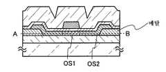
도 9는, 도 8에 도시하는 트랜지스터의 A-B 단면에 있어서의 에너지 밴드도(모식도)를 도시한다. 또한, 도 8은 실시 형태 2로 도시한 도 3과 동일한 또는 동 등한 것이다. 또한, 도 9의 (B)는 소스와 드레인 사이의 전압을 등전위(Vd=0V)로 한 경우를 도시하고 있다. 도 8은 제1 산화물 반도체 영역(OS1로 함) 및 한 쌍의 제2 산화물 반도체 영역(OS2로 함)으로 이루어지는 산화물 반도체막과, 소스 전극 및 드레인 전극(메탈(metal)로 함)에 의해 형성되는 트랜지스터이다.Fig. 9 shows an energy band diagram (schematic diagram) on the section A-B of the transistor shown in Fig. 8 is the same as or equivalent to Fig. 3 shown in the second embodiment. 9B shows a case where the voltage between the source and the drain is made equal potential (Vd = 0V). 8 shows an example in which an oxide semiconductor film composed of a first oxide semiconductor region (referred to as OS1) and a pair of second oxide semiconductor regions (referred to as OS2), and a source electrode and a drain electrode Lt; / RTI >
도 8에 있어서의 트랜지스터의 채널은 OS1에 의해 형성되어 있고, OS1은 막 내에서 수분(수소를 포함함) 등의 불순물을 가능한 한 제거, 탈리시켜서 고순도화함으로써 진성(I형)으로 한 것, 또는 한없이 진성에 접근한 산화물 반도체에 의해 형성되어 있다. 그렇게 함으로써 페르미 준위(Ef)는 진성 페르미 준위(Ei)와 동일한 레벨로 할 수 있다.The channel of the transistor in Fig. 8 is formed by OS1, OS1 is intrinsic (I type) by removing impurities such as moisture (including hydrogen) in the film as much as possible, Or oxide semiconductors approaching infinitely intrinsic. By doing so, the Fermi level Ef can be at the same level as the intrinsic Fermi level Ei.
또한, 도 8에 있어서의 트랜지스터의 소스 영역 및 드레인 영역은 한 쌍의 OS2에 의해 형성되어 있고, OS2는 상기 OS1과 마찬가지로, 막 중으로부터 수분(수소를 포함함) 등의 불순물을 가능한 한 제거, 탈리시켜서 고순도화함으로써 진성(I형)으로 한 것, 또는 한없이 진성에 접근한 산화물 반도체로 하고, 그 후, 수소 또는 희가스 중, 적어도 어느 하나 중에서 선택된 이온을 첨가함으로써 도너 또는 산소 결손을 발생하여 형성된다. 그에 의해, OS2는 OS1과 비교하여 캐리어 밀도가 높아지고, 페르미 준위의 위치가 전도대에 가깝게 된다.The source region and the drain region of the transistor in Fig. 8 are formed by a pair of OS2. OS2, like OS1, removes impurities such as moisture (including hydrogen) from the film as much as possible, (I-type) by making it high in purity or by making an oxide semiconductor approaching intrinsic nature infinitely, and then adding ions selected from at least one of hydrogen and rare gas to generate donor or oxygen deficiency do. As a result, the carrier density of the OS2 is higher than that of the OS1, and the position of the Fermi level is close to the conduction band.
도 9의 (A)는 진공 준위(Evac로 함), 제1 산화물 반도체 영역(OS1로 함), 제2 산화물 반도체 영역(OS2로 함), 및 소스 전극 및 드레인 전극(메탈로 함)의 밴드 구조의 관계이다. 여기서, IP는 이온화 포텐셜, Ea는 전자 친화력, Eg는 밴드 갭, Wf는 일함수를 나타낸다. 또한, Ec는 전도대의 하단부, Ev는 가전자대의 상단부, Ef는 페르미 준위를 나타낸다. 또한, 각 부호의 말미에 나타내는 기호는 1이 OS1을, 2가 OS2를, m이 메탈을 각각 나타낸다. 여기서 메탈로서 Wf_m이 4.1 eV(티타늄 등)를 상정하고 있다.9A shows a state in which a band of a vacuum level (referred to as Evac), a first oxide semiconductor region (referred to as OS1), a second oxide semiconductor region (referred to as OS2), and a source electrode and a drain electrode Structure. Here, IP denotes an ionization potential, Ea denotes an electron affinity, Eg denotes a band gap, and Wf denotes a work function. Ec represents the lower end of the conduction band, Ev represents the upper end of the valence band, and Ef represents the Fermi level. Symbols at the end of each symbol indicate OS1, OS2, and metal, respectively. Here, Wf_m is assumed to be 4.1 eV (such as titanium) as the metal.
OS1은 고순도화된 산화물 반도체이며, 지극히 캐리어 밀도가 낮기 때문에 Ef_1은 Ec 및 Ev의 대략 중앙에 있는 것으로 한다. 또한, OS2는 캐리어 밀도가 높은 n형의 산화물 반도체이며, Ec_2와 Ef_2가 대략 일치한다. OS1 및 OS2에 나타내는 산화물 반도체는 밴드 갭(Eg)이 3.15 eV, 전자 친화력(Ea)은 4.3 eV라고 말해지고 있다.Since OS1 is a high-purity oxide semiconductor and has extremely low carrier density, Ef_1 is assumed to be approximately at the center of Ec and Ev. OS2 is an n-type oxide semiconductor having a high carrier density, and Ec_2 and Ef_2 substantially coincide with each other. It is said that the bandgap Eg of the oxide semiconductor represented by OS1 and OS2 is 3.15 eV and the electron affinity Ea is 4.3 eV.
도 9의 (B)에 도시한 바와 같이, 채널인 OS1과, 소스 영역 및 드레인 영역인 OS2가 접촉하면, 페르미 준위가 일치하도록 캐리어의 이동이 일어나고, OS1 및 OS2의 밴드 단부가 구부러진다. 또한, OS2와, 소스 전극 및 드레인 전극인 메탈이 접촉한 경우에도, 페르미 준위가 일치하도록 캐리어의 이동이 일어나고, OS2의 밴드 단부가 구부러진다.As shown in Fig. 9B, when the channel OS1 is in contact with the OS2 serving as the source region and the drain region, the carriers move so that the Fermi levels coincide with each other, and the band ends of the OS1 and OS2 are bent. Further, even when the OS2 is in contact with the metal serving as the source electrode and the drain electrode, the carriers move so that the Fermi levels coincide with each other, and the band ends of the OS2 are bent.
이와 같이, 채널이 되는 OS1과 소스 전극 및 드레인 전극이 되는 메탈과의 사이에 n형의 산화물 반도체인 OS2가 형성됨으로써 산화물 반도체와 금속의 콘택트를 오믹으로 할 수 있고, 또한 콘택트 저항을 저감시킬 수 있다. 그 결과로서 트랜지스터의 온 전류를 증가시킬 수 있다. 또한, OS1의 밴드 단부의 구부러짐을 작게 할 수 있기 때문에, 트랜지스터의 단채널 효과를 저감할 수 있다.As described above, since the OS2, which is an n-type oxide semiconductor, is formed between the OS1 serving as a channel and the metal serving as the source electrode and the drain electrode, the contact between the oxide semiconductor and the metal can be made ohmic and the contact resistance can be reduced have. As a result, the ON current of the transistor can be increased. In addition, since the bend of the band end of the OS1 can be reduced, the short channel effect of the transistor can be reduced.
(실시 형태 7)(Seventh Embodiment)
도 10의 (A)에 반도체 장치를 구성하는 기억 소자(이하, 메모리 셀이라고도 기재함)의 회로도의 일례를 도시한다. 메모리 셀은 산화물 반도체 이외의 재료를 채널 형성 영역에 사용한 트랜지스터(1160)와 산화물 반도체를 채널 형성 영역에 사용한 트랜지스터(1162)로 구성된다.FIG. 10A shows an example of a circuit diagram of a memory element (hereinafter also referred to as a memory cell) constituting a semiconductor device. The memory cell is composed of a
산화물 반도체를 채널 형성 영역에 사용한 트랜지스터(1162)는 실시 형태 1 및 실시 형태 2에 따라서 제작할 수 있다.The
도 10의 (A)에 도시한 바와 같이, 트랜지스터(1160)의 게이트 전극과, 트랜지스터(1162)의 소스 전극 또는 드레인 전극 중 하나는 전기적으로 접속되어 있다. 또한, 제1 배선(1st Line: 소스선이라고도 칭함)이라고 트랜지스터(1160)의 소스 전극은 전기적으로 접속되고, 제2 배선(2nd Line: 비트선이라고도 칭함)과 트랜지스터(1160)의 드레인 전극은 전기적으로 접속되어 있다. 그리고, 제3 배선(3rd Line: 제1 신호선이라고도 칭함)과 트랜지스터(1162)의 소스 전극 또는 드레인 전극 중 다른 하나는 전기적으로 접속되고, 제4 배선(4th Line: 제2 신호선이라고도 칭함)과, 트랜지스터(1162)의 게이트 전극은 전기적으로 접속되어 있다.As shown in Fig. 10A, one of the gate electrode of the
산화물 반도체 이외의 재료, 예를 들어 단결정 실리콘을 채널 형성 영역에 사용한 트랜지스터(1160)는 충분한 고속 동작이 가능하기 때문에, 트랜지스터(1160)를 사용함으로써 기억 내용의 판독 등을 고속으로 행하는 것이 가능하다. 또한, 산화물 반도체를 채널 형성 영역에 사용한 트랜지스터(1162)는 트랜지스터(1160)에 비하여 오프 전류가 작다는 특징을 갖고 있다. 이로 인해, 트랜지스터(1162)를 오프 상태로 함으로써 트랜지스터(1160)의 게이트 전극의 전위를 지극히 장시간에 걸쳐 유지하는 것이 가능하다.Since the
게이트 전극의 전위가 유지 가능하다고 하는 특징을 살림으로써 다음과 같이, 정보의 기입, 유지, 판독이 가능하다.By storing the characteristic that the potential of the gate electrode is sustainable, it is possible to write, maintain and read information as follows.
처음에, 정보의 기입 및 유지에 대하여 설명한다. 우선, 제4 배선의 전위를 트랜지스터(1162)가 온 상태로 되는 전위로 하여 트랜지스터(1162)를 온 상태로 한다. 이에 의해, 제3 배선의 전위가 트랜지스터(1160)의 게이트 전극에 인가된다(기입). 그 후, 제4 배선의 전위를 트랜지스터(1162)가 오프 상태로 되는 전위로 하여 트랜지스터(1162)를 오프 상태로 함으로써 트랜지스터(1160)의 게이트 전극의 전위가 유지된다(유지).First, the writing and maintenance of information will be described. First, the potential of the fourth wiring is set to the potential at which the
트랜지스터(1162)의 오프 전류는 트랜지스터(1160)에 비하여 작기 때문에, 트랜지스터(1160)의 게이트 전극의 전위는 장시간에 걸쳐 유지된다. 예를 들어, 트랜지스터(1160)의 게이트 전극의 전위가 트랜지스터(1160)를 온 상태로 하는 전위이면, 트랜지스터(1160)의 온 상태가 장시간에 걸쳐 유지되게 된다. 또한, 트랜지스터(1160)의 게이트 전극의 전위가 트랜지스터(1160)를 오프 상태로 하는 전위이면, 트랜지스터(1160)의 오프 상태가 장시간에 걸쳐 유지된다.Since the off current of the
이어서, 정보의 판독에 대하여 설명한다. 상술한 바와 같이, 트랜지스터(1160)의 온 상태 또는 오프 상태가 유지된 상태에 있어서, 제1 배선에 소정의 전위(저전위)가 인가되면, 트랜지스터(1160)의 온 상태 또는 오프 상태에 따라 제2 배선의 전위는 상이한 값을 취한다. 예를 들어, 트랜지스터(1160)가 온 상태인 경우에는 제1 배선의 전위에 대하여 제2 배선의 전위가 저하하게 된다. 또한, 트랜지스터(1160)가 오프 상태인 경우에는 제2 배선의 전위는 변화하지 않는다.Next, the reading of information will be described. As described above, when a predetermined potential (low potential) is applied to the first wiring in the ON state or OFF state of the
이와 같이, 정보가 유지된 상태에 있어서, 제2 배선의 전위와 소정의 전위를 비교함으로써 정보를 판독할 수 있다.Thus, in a state in which information is held, information can be read by comparing the potential of the second wiring with a predetermined potential.
이어서, 정보의 재기입에 대하여 설명한다. 정보의 재기입은 상기 정보의 기입 및 유지와 마찬가지로 행해진다. 즉, 제4 배선의 전위를 트랜지스터(1162)가 온 상태로 되는 전위로 하여 트랜지스터(1162)를 온 상태로 한다. 이에 의해, 제3 배선의 전위(새로운 정보에 관한 전위)가 트랜지스터(1160)의 게이트 전극에 인가된다. 그 후, 제4 배선의 전위를 트랜지스터(1162)가 오프 상태로 되는 전위로 하여 트랜지스터(1162)를 오프 상태로 함으로써 새로운 정보가 유지된 상태로 된다.Next, rewriting of information will be described. The rewriting of information is performed in the same manner as the writing and maintenance of the information. That is, the potential of the fourth wiring is set to the potential at which the
이와 같이, 개시하는 발명에 따른 메모리 셀은, 다시 정보의 기입에 의해 직접 정보를 재기입하는 것이 가능하다. 이 때문에 플래시 메모리 등에 있어서 필요해지는 소거 동작이 불필요해서, 소거 동작에 기인하는 동작 속도의 저하를 억제할 수 있다. 즉, 메모리 셀을 갖는 반도체 장치의 고속 동작이 실현된다.As described above, the memory cell according to the disclosed invention can rewrite information directly by writing information again. Therefore, the erasing operation required in the flash memory or the like is unnecessary, and the lowering of the operating speed due to the erasing operation can be suppressed. That is, a high-speed operation of the semiconductor device having the memory cell is realized.
또한, 도 10의 (A)의 메모리 셀을 발전시킨 메모리 셀의 회로도의 일례를 도 10의 (B)에 도시하였다.FIG. 10 (B) shows an example of a circuit diagram of a memory cell in which the memory cell of FIG. 10 (A) is developed.
도 10의 (B)에 도시하는 메모리 셀(1100)은 제1 배선 SL(소스선)과, 제2 배선 BL(비트선)과, 제3 배선 S1(제1 신호선)과, 제4 배선 S2(제2 신호선)과, 제5 배선 WL(워드선)과, 트랜지스터(1164)(제1 트랜지스터)와, 트랜지스터(1161)(제2 트랜지스터)와, 트랜지스터(1163)(제3 트랜지스터)로 구성되어 있다. 트랜지스터(1164) 및 트랜지스터(1163)는 산화물 반도체 이외의 재료를 채널 형성 영역에 사용하고 있고, 트랜지스터(1161)는 산화물 반도체를 채널 형성 영역에 사용하고 있다.The
여기서, 트랜지스터(1164)의 게이트 전극과, 트랜지스터(1161)의 소스 전극 또는 드레인 전극 중 하나는 전기적으로 접속되어 있다. 또한, 제1 배선 SL과, 트랜지스터(1164)의 소스 전극은 전기적으로 접속되고, 트랜지스터(1164)의 드레인 전극과, 트랜지스터(1163)의 소스 전극은 전기적으로 접속되어 있다. 그리고, 제2 배선 BL과, 트랜지스터(1163)의 드레인 전극은 전기적으로 접속되고, 제3 배선 S1과, 트랜지스터(1161)의 소스 전극 또는 드레인 전극 중 다른 하나는 전기적으로 접속되고, 제4 배선 S2와, 트랜지스터(1161)의 게이트 전극은 전기적으로 접속되고, 제5 배선 WL과, 트랜지스터(1163)의 게이트 전극은 전기적으로 접속되어 있다.Here, the gate electrode of the
이어서, 회로의 동작에 대하여 구체적으로 설명한다.Next, the operation of the circuit will be described in detail.
메모리 셀(1100)에의 기입을 행하는 경우에는 제1 배선 SL을 0V, 제5 배선 WL을 0V, 제2 배선 BL을 0V, 제4 배선 S2를 2V로 한다. 데이터 "1"을 기입하는 경우에는 제3 배선 S1을 2V, 데이터 "0"을 기입하는 경우에는 제3 배선 S1을 0V로 한다. 이때, 트랜지스터(1163)는 오프 상태, 트랜지스터(1161)는 온 상태로 된다. 또한, 기입 종료에 있어서는, 제3 배선 S1의 전위가 변화하기 전에, 제4 배선 S2를 0V로 하여 트랜지스터(1161)를 오프 상태로 한다.In the case of writing in the
그 결과, 데이터 "1" 기입 후에는 트랜지스터(1164)의 게이트 전극에 접속되는 노드(이하, 노드 A)의 전위가 약 2V, 데이터 "0" 기입 후에는 노드 A의 전위가 약 0V가 된다. 노드 A에는 제3 배선 S1의 전위에 따른 전하가 축적되는데, 트랜지스터(1161)의 오프 전류는 단결정 실리콘을 채널 형성 영역에 사용한 트랜지스터와 비교하여 작고, 트랜지스터(1164)의 게이트 전극의 전위는 장시간에 걸쳐 유지된다.As a result, the potential of the node (hereinafter referred to as node A) connected to the gate electrode of the
이어서, 메모리 셀의 판독을 행하는 경우에는 제1 배선 SL을 0V, 제5 배선 WL을 2V, 제4 배선 S2를 0V, 제3 배선 S1을 0V로 하고, 제2 배선 BL에 접속되어 있는 판독 회로를 동작 상태로 한다. 이때, 트랜지스터(1163)는 온 상태, 트랜지스터(1161)는 오프 상태로 된다.Next, in the case of reading the memory cell, the first wiring SL is set to 0V, the fifth wiring WL is set to 2V, the fourth wiring S2 is set to 0V, the third wiring S1 is set to 0V, As shown in Fig. At this time, the
데이터 "0", 즉 노드 A가 약 0V의 상태이면 트랜지스터(1164)는 오프 상태이기 때문에, 제2 배선 BL과 제1 배선 SL간의 저항은 높은 상태가 된다. 한편, 데이터 "1", 즉 노드 A가 약 2V의 상태이면 트랜지스터(1164)가 온 상태이기 때문에, 제2 배선 BL과 제1 배선 SL 간의 저항은 낮은 상태가 된다. 판독 회로는 메모리 셀의 저항 상태의 차이로부터 데이터 "0", "1"을 판독할 수 있다. 또한, 기입 시의 제2 배선 BL은 0V로 했지만, 플로팅 상태나 0V 이상의 전위로 충전되어 있어도 상관없다. 판독 시의 제3 배선 S1은 0V로 했지만, 플로팅 상태나 0V 이상의 전위로 충전되어 있어도 상관없다.When the data "0 ", that is, when the node A is in the state of about 0 V, the
또한, 데이터 "1"과 데이터 "0"은 편의상의 정의이며, 반대이어도 상관없다. 또한, 상술한 동작 전압은 일례이다. 동작 전압은 데이터 "0"의 경우에 트랜지스터(1164)가 오프 상태로 되고, 데이터 "1"의 경우에 트랜지스터(1164)가 온 상태로 되도록, 또한 기입 시에 트랜지스터(1161)가 온 상태, 기입 시 이외에서는 오프 상태로 되도록, 또한 판독 시에 트랜지스터(1163)가 온 상태로 되도록 선택하면 된다. 특히 2V 대신에 주변의 논리 회로의 전원 전위 VDD를 사용해도 된다.The data "1" and the data "0" are definitions for convenience and may be reversed. The above-described operating voltage is an example. The operation voltage is set so that the
본 실시 형태에서는 이해하기 쉽게 하기 위하여, 최소 기억 단위(1비트)의 메모리 셀에 대하여 설명했지만, 메모리 셀의 구성은 이것에 한정되는 것은 아니다. 복수의 메모리 셀을 적절히 접속하여, 보다 고도의 반도체 장치를 구성할 수도 있다. 예를 들어, 상기 메모리 셀을 복수 사용하여, NAND형이나 NOR형의 반도체 장치를 구성하는 것이 가능하다. 배선의 구성도 도 10의 (A)이나 도 10의 (B)에 한정되지 않고, 적절히 변경할 수 있다.In this embodiment, a memory cell having a minimum memory unit (1 bit) has been described for easy understanding. However, the configuration of the memory cell is not limited to this. A plurality of memory cells may be suitably connected to constitute a higher-level semiconductor device. For example, it is possible to configure a NAND type or NOR type semiconductor device by using a plurality of the memory cells. The configuration of the wiring is not limited to those shown in Fig. 10 (A) or 10 (B), and can be appropriately changed.
도 11에 m×n 비트의 기억 용량을 갖는 본 발명의 일 형태에 따른 반도체 장치의 블록 회로도를 도시한다.11 shows a block circuit diagram of a semiconductor device according to an embodiment of the present invention having a storage capacity of m x n bits.
도 11에 도시하는 반도체 장치는, m개의 제5 배선 및 제4 배선과, n개의 제2 배선 및 제3 배선과, 복수의 메모리 셀(1100)(1, 1) 내지 (1100)(m, n)이 세로 m개행×가로 n개열(m, n은 자연수)의 매트릭스 형상으로 배치된 메모리 셀 어레이(1110)와, 제2 배선 및 제3 배선 구동 회로(1111)나, 제4 배선 및 제5 배선 구동 회로(1113)나, 판독 회로(1112)와 같은 주변 회로로 구성되어 있다. 다른 주변 회로로서 리프레시 회로 등이 형성되어도 된다.11 includes m fifth wiring and fourth wiring, n second wiring and third wiring, and a plurality of memory cells 1100 (1, 1) through 1100 (m, a
각 메모리 셀의 대표로서, 메모리 셀(1100)(i, j)을 생각한다. 여기서, 메모리 셀(1100)(i, j)(i는 1 이상 m 이하의 정수, j는 1 이상 n 이하의 정수)은 제2 배선 BL(j), 제3 배선 S1(j), 제5 배선 WL(i) 및 제4 배선 S2(i), 및 제1 배선에 각각 접속되어 있다. 제1 배선에는 제1 배선 전위 Vs가 인가되어 있다. 또한, 제2 배선 BL(1) 내지 BL(n) 및 제3 배선 S1(1) 내지 S1(n)은 제2 배선 및 제3 배선 구동 회로(1111) 및 판독 회로(1112)에, 제5 배선 WL(1) 내지 WL(m) 및 제4 배선 S2(1) 내지 S2(m)은 제4 배선 및 제5 배선 구동 회로(1113)에 각각에 접속되어 있다.As a representative of each memory cell, a memory cell 1100 (i, j) is considered. Here, the memory cell 1100 (i, j) (i is an integer equal to or greater than 1 and equal to or smaller than m, and j is an integer equal to or greater than 1 and equal to or less than n) is referred to as a second wiring BL (j) The wirings WL (i), the fourth wirings S2 (i), and the first wirings. The first wiring potential Vs is applied to the first wiring. The second wirings BL (1) to BL (n) and the third wirings S1 (1) to S1 (n) are connected to the second wiring and the third
도 11에 도시한 반도체 장치의 동작에 대하여 설명한다. 본 구성에서는, 행 마다의 기입 및 판독을 행한다.The operation of the semiconductor device shown in Fig. 11 will be described. In this configuration, writing and reading are performed for each row.
제i행의 메모리 셀(1100)(i, 1) 내지 (1100)(i, n)에 기입을 행하는 경우에는 제1 배선 전위 Vs를 0V, 제5 배선 WL(i)을 0V, 제2 배선 BL(1) 내지 BL(n)을 0V, 제4 배선 S2(i)을 2V로 한다. 이때 트랜지스터(1161)는 온 상태로 된다. 제3 배선 S1(1) 내지 S1(n)은 데이터 "1"을 기입하는 열은 2V, 데이터 "0"을 기입하는 열은 0V로 한다. 또한, 기입 종료에 있어서는, 제3 배선 S1(1) 내지 S1(n)의 전위가 변화하기 전에, 제4 배선 S2(i)을 0V로 하여 트랜지스터(1161)를 오프 상태로 한다. 또한, 비선택의 제5 배선 WL은 0V, 비선택의 제4 배선 S2는 0V로 한다.The first wiring potential Vs is 0 V, the fifth wiring WL (i) is 0 V, and the first wiring potential Vs is 0 V. When writing is performed to the memory cells 1100 (i, 1) to 1100 BL (1) to BL (n) are set to 0V, and the fourth wiring S2 (i) is set to 2V. At this time, the
그 결과, 데이터 "1"의 기입을 행한 메모리 셀의 트랜지스터(1164)의 게이트 전극에 접속되는 노드(이하, 노드 A)의 전위는 약 2V, 데이터 "0"의 기입을 행한 메모리 셀의 노드 A의 전위는 약 0V가 된다. 또한, 비선택 메모리 셀의 노드 A의 전위는 변함없다.As a result, the potential of the node (hereinafter node A) connected to the gate electrode of the
제i행의 메모리 셀(1100)(i, 1) 내지 (1100)(i, n)의 판독을 행하는 경우에는 제1 배선 전위 Vs를 0V, 제5 배선 WL(i)을 2V, 제4 배선 S2(i)을 0V, 제3 배선 S1(1) 내지 S1(n)을 0V로 하고, 제2 배선 BL(1) 내지 BL(n)에 접속되어 있는 판독 회로를 동작 상태로 한다. 판독 회로에서는, 예를 들어, 메모리 셀의 저항 상태의 차이로, 데이터 "0", "1"을 판독할 수 있다. 또한, 비선택의 제5 배선 WL은 0V, 비선택의 제4 배선은 0V로 한다. 또한, 기입 시의 제2 배선 BL은 0V로 했지만, 플로팅 상태나 0V 이상의 전위로 충전되어 있어도 상관없다. 판독 시의 제3 배선 S1은 0V로 했지만, 플로팅 상태나 0V 이상의 전위로 충전되어 있어도 상관없다.In the case of reading the memory cells 1100 (i, 1) to 1100 (i, n) in the i-th row, the first wiring potential Vs is 0 V, the fifth wiring WL (i) S2 (i) is 0 V, the third wirings S1 (1) to S1 (n) are 0 V, and the reading circuit connected to the second wirings BL (1) to BL (n) is put into an operating state. In the reading circuit, for example, data "0" and "1" can be read out due to the difference in the resistance state of the memory cell. The non-selected fifth wiring WL is set to 0 V, and the unselected fourth wiring is set to 0 V. [ Although the second wiring BL at the time of writing is set to 0 V, it may be filled in a floating state or a potential higher than 0 V. [ Although the third wiring S1 at the time of reading is set to 0 V, it may be filled in a floating state or a potential higher than 0V.
또한, 데이터 "1"과 데이터 "0"은 편의상의 정의이며, 반대이어도 상관없다. 또한, 상술한 동작 전압은 일례이다. 동작 전압은 데이터 "0"의 경우에 트랜지스터(1164)가 오프 상태로 되고, 데이터 "1"의 경우에 트랜지스터(1164)가 온 상태로 되도록, 또한 기입 시에 트랜지스터(1161)가 온 상태, 기입 시 이외에서는 오프 상태로 되도록, 또한 판독 시에 트랜지스터(1163)가 온 상태로 되도록 선택하면 된다. 특히 2V 대신에 주변의 논리 회로의 전원 전위 VDD를 사용해도 된다.The data "1" and the data "0" are definitions for convenience and may be reversed. The above-described operating voltage is an example. The operation voltage is set so that the
(실시 형태 8)(Embodiment 8)
본 실시 형태에서는 용량 소자를 갖는 메모리 셀의 회로도의 일례를 도시한다. 도 12의 (A)에 도시하는 메모리 셀(1170)은 제1 배선 SL, 제2 배선 BL, 제3 배선 S1, 제4 배선 S2와, 제5 배선 WL과, 트랜지스터(1171)(제1 트랜지스터)와, 트랜지스터(1172)(제2 트랜지스터)와, 용량 소자(1173)로 구성되어 있다. 트랜지스터(1171)는 산화물 반도체 이외의 재료를 채널 형성 영역에 사용하고 있고, 트랜지스터(1172)는 채널 형성 영역에 산화물 반도체를 사용하고 있다.In the present embodiment, an example of a circuit diagram of a memory cell having a capacitor element is shown. The
여기서, 트랜지스터(1171)의 게이트 전극과, 트랜지스터(1172)의 소스 전극 또는 드레인 전극의 한쪽과, 용량 소자(1173)의 한쪽의 전극은 전기적으로 접속되어 있다. 또한, 제1 배선 SL과, 트랜지스터(1171)의 소스 전극은 전기적으로 접속되고, 제2 배선 BL과, 트랜지스터(1171)의 드레인 전극은 전기적으로 접속되고, 제3 배선 S1과, 트랜지스터(1172)의 소스 전극 또는 드레인 전극의 다른쪽은 전기적으로 접속되고, 제4 배선 S2와, 트랜지스터(1172)의 게이트 전극은 전기적으로 접속되고, 제5 배선 WL과, 용량 소자(1173)의 다른쪽의 전극은 전기적으로 접속되어 있다.Here, the gate electrode of the
이어서, 회로의 동작에 대하여 구체적으로 설명한다.Next, the operation of the circuit will be described in detail.
메모리 셀(1170)에의 기입을 행하는 경우에는 제1 배선 SL을 0V, 제5 배선 WL을 0V, 제2 배선 BL을 0V, 제4 배선 S2를 2V로 한다. 데이터 "1"을 기입하는 경우에는 제3 배선 S1을 2V, 데이터 "0"을 기입하는 경우에는 제3 배선 S1을 0V로 한다. 이때, 트랜지스터(1172)는 온 상태로 된다. 또한, 기입 종료에 있어서는, 제3 배선 S1의 전위가 변화하기 전에, 제4 배선 S2를 0V로 하여 트랜지스터(1172)을 오프 상태로 한다.In the case of writing in the
그 결과, 데이터 "1"의 기입 후에는 트랜지스터(1171)의 게이트 전극에 접속되는 노드(이하, 노드 A)의 전위가 약 2V, 데이터 "0"의 기입 후에는 노드 A의 전위가 약 0V가 된다.As a result, after the writing of the data " 1 ", the potential of the node (hereinafter, node A) connected to the gate electrode of the
메모리 셀(1170)의 판독을 행하는 경우에는 제1 배선 SL을 0V, 제5 배선 WL을 2V, 제4 배선 S2를 0V, 제3 배선 S1을 0V로 하고, 제2 배선 BL에 접속되어 있는 판독 회로를 동작 상태로 한다. 이때, 트랜지스터(1172)는 오프 상태로 된다.When the
제5 배선 WL을 2V로 한 경우의 트랜지스터(1171)의 상태에 대하여 설명한다. 트랜지스터(1171)의 상태를 정하는 노드 A의 전위는 제5 배선 WL-노드 A 간의 용량 C1과, 트랜지스터(1171)의 게이트 전극- 소스 전극과 드레인 전극 간의 용량 C2에 의존한다.The state of the
또한, 판독 시의 제3 배선 S1은 0V로 했지만, 플로팅 상태나 0V 이상의 전위로 충전되어 있어도 상관없다. 데이터 "1"과 데이터 "0"은 편의상의 정의이며, 반대이어도 상관없다.Further, although the third wiring S1 at the time of reading is set to 0 V, it may be filled in a floating state or a potential higher than 0V. Data "1" and data "0" are defined for convenience and may be reversed.
기입 시의 제3 배선 S1의 전위는 기입 후에 트랜지스터(1172)가 오프 상태로 되고 또한 제5 배선 WL의 전위가 0V인 경우에 트랜지스터(1171)가 오프 상태인 범위에서 데이터 "0", "1"의 전위를 각각 선택하면 된다. 판독 시의 제5 배선 WL 전위는 데이터 "0"의 경우에 트랜지스터(1171)이 오프 상태로 되고, 데이터 "1"의 경우에 트랜지스터(1171)이 온 상태로 되도록 선택하면 된다. 또한, 트랜지스터(1171)의 임계값 전압도 일례이다. 상술한 트랜지스터(1171)의 상태를 바꾸지 않는 범위이면, 어떤 임계값이어도 상관없다.0 ", "1 ", and " 1 " in the range where the
또한, 제1 게이트 전극, 및 제2 게이트 전극을 갖는 선택 트랜지스터와, 용량 소자를 갖는 메모리 셀을 사용하는 NOR형의 반도체 기억 장치의 예에 대하여 도 12의 (B)를 사용하여 설명한다.An example of a NOR type semiconductor memory device using a selection transistor having a first gate electrode and a second gate electrode and a memory cell having a capacitor element will be described with reference to FIG. 12 (B).
도 12의 (B)에 도시하는 본 발명의 일 형태에 따른 반도체 장치는 i행(i는 2 이상의 자연수) j열(j는 자연수)로 매트릭스 형상으로 배열된 복수의 메모리 셀을 구비한 메모리 셀 어레이를 구비한다.A semiconductor device according to an embodiment of the present invention shown in Fig. 12B includes a memory cell having a plurality of memory cells arranged in a matrix with i rows (i is a natural number of 2 or more) j columns (j is a natural number) Array.
도 12의 (B)에 도시하는 메모리 셀 어레이는, i행(i는 3 이상의 자연수) j열(j는 3 이상의 자연수)에 매트릭스 형상으로 배열된 복수의 메모리 셀(1180)과, i개의 워드선 WL(워드선 WL_1 내지 워드선 WL_i)과, i개의 용량선 CL(용량선 CL_1 내지 용량선 CL_i)과, i개의 게이트선 BGL(게이트선 BGL_1 내지 게이트선 BGL_i)과, j개의 비트선 BL(비트선 BL_1 내지 비트선 BL_j)과, 소스선 SL을 구비한다.The memory cell array shown in Fig. 12B includes a plurality of
또한, 복수의 메모리 셀(1180)의 각각(메모리 셀(1180)(M, N)(단, N은 1 이상 j 이하의 자연수, M은 1 이상 i 이하의 자연수)이라고도 함)은 트랜지스터(1181)(M, N)와, 용량 소자(1183)(M, N)와, 트랜지스터(1182)(M, N)를 구비한다.Each of the plurality of memory cells 1180 (also referred to as a memory cell 1180 (M, N) (where N is a natural number of 1 or more and j or less and M is a natural number of 1 or more and i or less) (M, N), capacitive elements 1183 (M, N), and transistors 1182 (M, N).
또한, 반도체 기억 장치에 있어서, 용량 소자는 제1 용량 전극, 제2 용량 전극, 및 제1 용량 전극 및 제2 용량 전극에 중첩하는 유전체층으로 구성된다. 용량 소자는 제1 용량 전극 및 제2 용량 전극 간에 인가되는 전압에 따라서 전하가 축적된다.In the semiconductor memory device, the capacitor element is composed of a first capacitor electrode, a second capacitor electrode, and a dielectric layer overlapping the first capacitor electrode and the second capacitor electrode. Charges are accumulated in accordance with the voltage applied between the first capacitor electrode and the second capacitor electrode.
트랜지스터(1181)(M, N)은 N 채널형 트랜지스터이며, 소스 전극, 드레인 전극, 제1 게이트 전극, 및 제2 게이트 전극을 갖는다. 또한, 본 실시 형태의 반도체 기억 장치에 있어서, 반드시 트랜지스터(1181)를 N 채널형 트랜지스터로 하지 않아도 된다.The transistor 1181 (M, N) is an N-channel transistor and has a source electrode, a drain electrode, a first gate electrode, and a second gate electrode. In the semiconductor memory device of the present embodiment, the
트랜지스터(1181)(M, N)의 소스 전극 및 드레인 전극 중 하나는 비트선 BL_N에 접속되고, 트랜지스터(1181)(M, N)의 제1 게이트 전극은 워드선 WL_M에 접속되고, 트랜지스터(1181)(M, N)의 제2 게이트 전극은 게이트선 BGL_M에 접속된다. 트랜지스터(1181)(M, N)의 소스 전극 및 드레인 전극 중 하나가 비트선 BL_N에 접속되는 구성으로 함으로써 메모리 셀마다 선택적으로 데이터를 판독할 수 있다.One of the source electrode and the drain electrode of the transistor 1181 (M, N) is connected to the bit line BL_N, the first gate electrode of the transistor 1181 (M, N) is connected to the word line WL_M, ) (M, N) is connected to the gate line BGL_M. And one of the source electrode and the drain electrode of the transistor 1181 (M, N) is connected to the bit line BL_N, whereby data can be selectively read for each memory cell.
트랜지스터(1181)(M, N)은 메모리 셀(1180)(M, N)에 있어서 선택 트랜지스터로서의 기능을 갖는다.Transistors 1181 (M, N) have a function as select transistors in memory cells 1180 (M, N).
트랜지스터(1181)(M, N)로서는, 산화물 반도체를 채널 형성 영역에 사용한 트랜지스터를 사용할 수 있다.As the transistor 1181 (M, N), a transistor using an oxide semiconductor as a channel forming region can be used.
트랜지스터(1182)(M, N)은 P 채널형 트랜지스터이다. 또한, 본 실시 형태의 반도체 기억 장치에 있어서, 반드시 트랜지스터(1182)을 P 채널형 트랜지스터로 하지 않아도 된다.Transistors 1182 (M, N) are P-channel transistors. In the semiconductor memory device of the present embodiment, the
트랜지스터(1182)(M, N)의 소스 전극 및 드레인 전극 중 하나는 소스선 SL에 접속되고, 트랜지스터(1182)(M, N)의 소스 전극 및 드레인 전극 중 다른 하나는 비트선 BL_N에 접속되고, 트랜지스터(1182)(M, N)의 게이트 전극은 트랜지스터(1181)(M, N)의 소스 전극 및 드레인 전극 중 다른 하나에 접속된다.One of the source electrode and the drain electrode of the transistor 1182 (M, N) is connected to the source line SL, and the other of the source electrode and the drain electrode of the transistor 1182 (M, N) is connected to the bit line BL_N , The gate electrode of transistor 1182 (M, N) is connected to the other of the source electrode and the drain electrode of transistor 1181 (M, N).
트랜지스터(1182)(M, N)은 메모리 셀(1180)(M, N)에 있어서, 출력 트랜지스터로서의 기능을 갖는다. 트랜지스터(1182)(M, N)로서는, 예를 들어 단결정 실리콘을 채널 형성 영역에 사용하는 트랜지스터를 사용할 수 있다.Transistor 1182 (M, N) has a function as an output transistor in memory cell 1180 (M, N). As the transistor 1182 (M, N), for example, a transistor using a single crystal silicon in a channel forming region can be used.
용량 소자(1183)(M, N)의 제1 용량 전극은 용량선 CL_M에 접속되고, 용량 소자(1183)(M, N)의 제2 용량 전극은 트랜지스터(1181)(M, N)의 소스 전극 및 드레인 전극의 다른쪽에 접속된다. 또한, 용량 소자(1183)(M, N)은 유지 용량으로서의 기능을 갖는다.The first capacitive electrode of the capacitive element 1183 (M, N) is connected to the capacitive line CL_M and the second capacitive electrode of the capacitive element 1183 (M, N) is connected to the source of the
워드선 WL_1 내지 워드선 WL_i 각각의 전압은 예를 들어 디코더를 사용한 구동 회로에 의해 제어된다.The voltage of each of the word lines WL_1 to WL_i is controlled by, for example, a driving circuit using a decoder.
비트선 BL_1 내지 비트선 BL_j 각각의 전압은 예를 들어 디코더를 사용한 구동 회로에 의해 제어된다.The voltages of the bit lines BL_1 to BL_j are controlled by, for example, a driving circuit using a decoder.
용량선 CL_1 내지 용량선 CL_i 각각의 전압은 예를 들어 디코더를 사용한 구동 회로에 의해 제어된다.The voltage of each of the capacitance lines CL_1 to CL_i is controlled by, for example, a driving circuit using a decoder.
게이트선 BGL_1 내지 게이트선 BGL_i 각각의 전압은 예를 들어 게이트선 구동 회로를 사용하여 제어된다.The voltages of the gate lines BGL_1 to BGL_i are controlled using, for example, a gate line driving circuit.
게이트선 구동 회로는 예를 들어 다이오드 및 제1 용량 전극이 다이오드의 애노드 및 게이트선 BGL에 전기적으로 접속되는 용량 소자를 구비하는 회로로 구성된다.The gate line driving circuit is constituted by, for example, a circuit including a diode and a capacitor element in which the first capacitor electrode is electrically connected to the anode and the gate line BGL of the diode.
트랜지스터(1181)의 제2 게이트 전극의 전압을 조정함으로써 트랜지스터(1181)의 임계값 전압을 조정할 수 있다. 따라서, 선택 트랜지스터로서 기능하는 트랜지스터(1181)의 임계값 전압을 조정하여, 오프 상태에 있어서의 트랜지스터(1181)의 소스 전극 및 드레인 전극 사이에 흐르는 전류를 최대한 작게 할 수 있다. 따라서, 기억 회로에 있어서의 데이터의 유지 기간을 길게 할 수 있다. 또한, 데이터의 기입 및 판독에 필요한 전압을 종래의 반도체 장치보다 낮게 할 수 있기 때문에, 소비 전력을 저감할 수 있다.The threshold voltage of the
(실시 형태 9)(Embodiment 9)
본 실시 형태에서는 상기한 실시 형태에 나타내는 트랜지스터를 사용한 반도체 장치의 예에 대해서 도 13을 참조하여 설명한다.In this embodiment, an example of a semiconductor device using the transistor shown in the above embodiment will be described with reference to Fig.
도 13의 (A)에는 소위 DRAM(Dynamic Random Access Memory)에 상당하는 구성의 반도체 장치의 일례를 도시한다. 도 13의 (A)에 도시하는 메모리 셀 어레이(1120)는 복수의 메모리 셀(1130)이 매트릭스 형상으로 배열된 구성을 갖고 있다. 또한, 메모리 셀 어레이(1120)은 m개의 제1 배선, 및 n개의 제2 배선을 갖는다. 또한, 본 실시 형태에 있어서는, 제1 배선을 비트선 BL이라 칭하고, 제2 배선을 워드선 WL이라 칭한다.FIG. 13A shows an example of a semiconductor device having a configuration corresponding to a so-called DRAM (Dynamic Random Access Memory). A
메모리 셀(1130)은 트랜지스터(1131)와, 용량 소자(1132)로 구성되어 있다. 트랜지스터(1131)의 게이트 전극은 제1 배선(워드선 WL)과 접속되어 있다. 또한, 트랜지스터(1131)의 소스 전극 또는 드레인 전극 중 하나는 제2 배선(비트선 BL)과 접속되어 있고, 트랜지스터(1131)의 소스 전극 또는 드레인 전극 중 다른 하나는 용량 소자의 한쪽 전극과 접속되어 있다. 또한, 용량 소자의 다른쪽 전극은 용량선 CL과 접속되고, 일정한 전위가 인가되어 있다. 트랜지스터(1131)에는 전번의 실시 형태에 나타내는 트랜지스터가 적용된다.The
전번의 실시 형태에 있어서 나타낸 산화물 반도체를 채널 형성 영역에 사용하는 트랜지스터는 단결정 실리콘을 채널 형성 영역에 사용한 트랜지스터에 비하여 오프 전류가 작다는 특징을 갖는다. 이로 인해, 소위 DRAM으로서 인식되어 있는 도 13의 (A)에 도시하는 반도체 장치에 상기 트랜지스터를 적용하는 경우, 실질적인 불휘발성 메모리를 얻는 것이 가능하다.The transistor using the oxide semiconductor in the channel forming region shown in the previous embodiment is characterized in that the off current is smaller than that of the transistor using single crystal silicon in the channel forming region. Therefore, when the transistor is applied to the semiconductor device shown in Fig. 13A which is recognized as a so-called DRAM, it is possible to obtain a substantial nonvolatile memory.
도 13의 (B)에는 소위 SRAM(Static Random Access Memory)에 상당하는 구성의 반도체 장치의 일례를 도시한다. 도 13의 (B)에 도시하는 메모리 셀 어레이(1140)는 복수의 메모리 셀(1150)이 매트릭스 형상으로 배열된 구성으로 할 수 있다. 또한, 메모리 셀 어레이(1140)는 제1 배선(워드선 WL), 제2 배선(비트선 BL) 및 제3 배선(반전 비트선/BL)을 각각 복수개 갖는다.FIG. 13B shows an example of a semiconductor device having a configuration corresponding to a so-called static random access memory (SRAM). The
메모리 셀(1150)은 제1 트랜지스터(1151), 제2 트랜지스터(1152), 제3 트랜지스터(1153), 제4 트랜지스터(1154), 제5 트랜지스터(1155), 및 제6 트랜지스터(1156)를 갖고 있다. 제1 트랜지스터(1151)와 제2 트랜지스터(1152)는 선택 트랜지스터로서 기능한다. 또한, 제3 트랜지스터(1153)와 제4 트랜지스터(1154) 중, 한쪽은 n채널형 트랜지스터(여기서는, 제4 트랜지스터(1154))이며, 다른쪽은 p채널형 트랜지스터(여기서는, 제3 트랜지스터(1153))이다. 즉, 제3 트랜지스터(1153)와 제4 트랜지스터(1154)에 의해 CMOS 회로가 구성되어 있다. 마찬가지로, 제5 트랜지스터(1155)과 제6 트랜지스터(1156)에 의해 CMOS 회로가 구성되어 있다.The
제1 트랜지스터(1151), 제2 트랜지스터(1152), 제4 트랜지스터(1154), 제6 트랜지스터(1156)는 n채널형의 트랜지스터이며, 전번의 실시 형태에 있어서 나타낸 트랜지스터를 적용할 수 있다. 제3 트랜지스터(1153)와 제5 트랜지스터(1155)는 p채널형의 트랜지스터이며, 산화물 반도체 이외의 재료(예를 들어, 단결정 실리콘 등)를 채널 형성 영역에 사용한다.The
본 실시 형태에 나타내는 구성, 방법 등은 다른 실시 형태에 나타내는 구성, 방법 등과 적절히 조합하여 사용할 수 있다.The configurations, methods, and the like described in this embodiment can be appropriately combined with the configurations, methods, and the like described in the other embodiments.
(실시 형태 10)(Embodiment 10)
산화물 반도체를 채널 형성 영역에 사용한 트랜지스터를 적어도 일부에 사용하여 CPU(Central Processing Unit)를 구성할 수 있다.A CPU (Central Processing Unit) can be constituted by using at least a part of the transistor in which the oxide semiconductor is used as the channel forming region.
도 14의 (A)는 CPU의 구체적인 구성을 도시하는 블록도이다. 도 14의 (A)에 도시하는 CPU는 기판(1190) 위에 연산 회로(ALU: Arithmetic logic unit)(1191), ALU 컨트롤러(1192), 인스트럭션 디코더(1193), 인터럽트 컨트롤러(1194), 타이밍 컨트롤러(1195), 레지스터(1196), 레지스터 컨트롤러(1197), 버스 인터페이스(Bus I/F)(1198), 재기입 가능한 ROM (1199), 및 ROM 인터페이스(ROM I/F)(1189)를 갖고 있다. 기판(1190)은 반도체 기판, SOI 기판, 유리 기판 등을 사용한다. ROM (1199) 및 ROM I/F(1189)는 별도의 칩에 실장해도 된다. 물론, 도 14의 (A)에 도시하는 CPU는 그의 구성을 간략화하여 나타낸 일례에 지나지 않고, 실제의 CPU는 그의 용도에 따라 다종다양한 구성을 갖고 있다.14 (A) is a block diagram showing a specific configuration of a CPU. The CPU shown in Fig. 14A includes an arithmetic logic unit (ALU) 1191, an
버스 인터페이스(1198)을 통하여 CPU에 입력된 명령은, 인스트럭션 디코더(1193)에 입력되고, 디코드된 후, ALU 컨트롤러(1192), 인터럽트 컨트롤러(1194), 레지스터 컨트롤러(1197), 타이밍 컨트롤러(1195)에 입력된다.The instruction input to the CPU via the
ALU 컨트롤러(1192), 인터럽트 컨트롤러(1194), 레지스터 컨트롤러(1197), 타이밍 컨트롤러(1195)는 디코드된 명령에 기초하여 각종 제어를 행한다. 구체적으로 ALU 컨트롤러(1192)은 ALU(1191)의 동작을 제어하기 위한 신호를 생성한다. 또한, 인터럽트 컨트롤러(1194)은 CPU의 프로그램 실행 중에, 외부의 입출력 장치나, 주변 회로로부터의 인터럽트 요구를, 그의 우선도나 마스크 상태로부터 판단하여 처리한다. 레지스터 컨트롤러(1197)는 레지스터(1196)의 어드레스를 생성하고, CPU의 상태에 따라서 레지스터(1196)의 판독이나 기입을 행한다.The
또한, 타이밍 컨트롤러(1195)는 ALU(1191), ALU 컨트롤러(1192), 인스트럭션 디코더(1193), 인터럽트 컨트롤러(1194), 및 레지스터 컨트롤러(1197)의 동작의 타이밍을 제어하는 신호를 생성한다. 예를 들어 타이밍 컨트롤러(1195)는 기준 클록 신호 CLK1을 바탕으로, 내부 클록 신호 CLK2를 생성하는 내부 클록 생성부를 구비하고 있고, 클록 신호 CLK2를 상기 각종 회로에 공급한다.The
도 14의 (A)에 도시하는 CPU에서는 레지스터(1196)에 기억 소자가 형성되어 있다. 레지스터(1196)의 기억 소자에는 실시 형태 7에 기재되어 있는 기억 소자를 사용할 수 있다.A memory element is formed in the
도 14의 (A)에 도시하는 CPU에 있어서, 레지스터 컨트롤러(1197)는 ALU(1191)로부터의 지시에 따라, 레지스터(1196)에 있어서의 유지 동작의 선택을 행한다. 즉, 레지스터(1196)가 갖는 기억 소자에 있어서, 위상 반전 소자에 의한 데이터의 유지를 행할 것인가, 용량 소자에 의한 데이터의 유지를 행할 것인가를 선택한다. 위상 반전 소자에 의한 데이터의 유지가 선택되어 있는 경우, 레지스터(1196) 내의 기억 소자에의 전원 전압의 공급이 행해진다. 용량 소자에 있어서의 데이터의 유지가 선택되어 있는 경우, 용량 소자에의 데이터의 재기입이 행해지고, 레지스터(1196) 내의 기억 소자에의 전원 전압의 공급을 정지할 수 있다.In the CPU shown in FIG. 14A, the
전원 정지에 대해서는, 도 14의 (B) 또는 도 14의 (C)에 도시한 바와 같이, 기억 소자군과, 전원 전위 VDD 또는 전원 전위 VSS가 인가되어 있는 노드 사이에 스위칭 소자를 설치함으로써 행할 수 있다. 이하에 도 14의 (B) 및 도 14의 (C)의 회로의 설명을 행한다.As for the power supply stop, as shown in Fig. 14B or 14C, a switching element can be provided between the memory element group and the node to which the power source potential VDD or the power source potential VSS is applied have. The circuit of Fig. 14 (B) and Fig. 14 (C) will be described below.
도 14의 (B) 및 도 14의 (C)에서는 기억 소자에의 전원 전위의 공급을 제어하는 스위칭 소자에, 산화물 반도체를 채널 형성 영역에 사용한 트랜지스터를 포함하는 기억 회로의 구성의 일례를 도시한다.14B and 14C show an example of a configuration of a memory circuit including a transistor in which an oxide semiconductor is used as a channel forming region in a switching element for controlling supply of a power source potential to a memory element .
도 14의 (B)에 도시하는 기억 장치는 스위칭 소자(1141)와, 기억 소자(1142)를 복수 갖는 기억 소자군(1143)을 갖고 있다. 구체적으로, 각 기억 소자(1142)에는 실시 형태 7에 기재되어 있는 기억 소자를 사용할 수 있다. 기억 소자군(1143)이 갖는 각 기억 소자(1142)에는 스위칭 소자(1141)를 통하여 하이 레벨의 전원 전위 VDD가 공급되고 있다. 또한, 기억 소자군(1143)이 갖는 각 기억 소자(1142)에는 신호 IN의 전위와, 로우 레벨의 전원 전위 VSS의 전위가 인가되어 있다.14 (B) has a
도 14의 (B)에서는 스위칭 소자(1141)로서, 산화물 반도체를 채널 형성 영역에 갖는 트랜지스터를 사용하고 있고, 상기 트랜지스터는 그의 게이트 전극에 인가되는 신호 SigA에 의해 스위칭이 제어된다.14B, a transistor having an oxide semiconductor in a channel forming region is used as the
또한, 도 14의 (B)에서는 스위칭 소자(1141)가 트랜지스터를 하나만 갖는 구성을 나타내고 있지만, 특별히 한정되지 않고 트랜지스터를 복수 갖고 있어도 된다. 스위칭 소자(1141)가 스위칭 소자로서 기능하는 트랜지스터를 복수 갖고 있는 경우, 상기 복수의 트랜지스터는 병렬로 접속되어 있어도 되고, 직렬로 접속되어 있어도 되고, 직렬과 병렬이 조합되어서 접속되어 있어도 된다.14B shows a configuration in which the
또한, 도 14의 (B)에서는 스위칭 소자(1141)에 의해, 기억 소자군(1143)이 갖는 각 기억 소자(1142)에의, 하이 레벨의 전원 전위 VDD의 공급이 제어되고 있지만, 스위칭 소자(1141)에 의해, 로우 레벨의 전원 전위 VSS의 공급이 제어되고 있어도 된다.14B, the supply of the high-level power supply potential VDD to each
또한, 도 14의 (C)에는 기억 소자군(1143)이 갖는 각 기억 소자(1142)에 스위칭 소자(1141)를 통하여 로우 레벨의 전원 전위 VSS가 공급되고 있는 기억 장치의 일례를 도시한다. 스위칭 소자(1141)에 의해 기억 소자군(1143)이 갖는 각 기억 소자(1142)에의, 로우 레벨의 전원 전위 VSS의 공급을 제어할 수 있다.14C shows an example of a storage device in which a low-level power supply potential VSS is supplied to each
기억 소자군과, 전원 전위 VDD 또는 전원 전위 VSS가 인가되어 있는 노드 사이에 스위칭 소자를 설치하여, 일시적으로 CPU의 동작을 정지하여, 전원 전압의 공급을 정지한 경우에 있어서도 데이터를 유지하는 것이 가능하여, 소비 전력의 저감을 행할 수 있다. 구체적으로는, 예를 들어, 퍼스널 컴퓨터의 유저가 키보드 등의 입력 장치에의 정보의 입력을 정지하고 있는 동안에도 CPU의 동작을 정지할 수 있고, 그것에 의해 소비 전력을 저감할 수 있다.It is possible to maintain the data even when the switching element is provided between the memory element group and the node to which the power source potential VDD or the power source potential VSS is applied to temporarily stop the operation of the CPU to stop the supply of the power source voltage So that the power consumption can be reduced. Specifically, for example, while the user of the personal computer stops inputting information to an input device such as a keyboard, the operation of the CPU can be stopped, thereby reducing power consumption.
여기에서는, CPU를 예로 들어 설명했지만, DSP(Digital Signal Processor), 커스텀 LSI, FPGA(Field Programmable Gate Array) 등의 LSI로도 응용가능하다.Although the CPU has been described as an example here, it can be applied to an LSI such as a DSP (Digital Signal Processor), a custom LSI, and an FPGA (Field Programmable Gate Array).
본 실시 형태는 상기 실시 형태와 적절히 조합하여 실시하는 것이 가능하다.The present embodiment can be implemented in appropriate combination with the above embodiment.
100: 기판
102: 하지 절연막
112: 게이트 절연막
114: 게이트 전극
116: 배선
122: 산화물 반도체 영역
124: 층간 절연막
126: 산화물 반도체 영역
130: 콘택트 홀
140: 산화물 반도체막
150: 이온
151: 트랜지스터
152: 트랜지스터
153: 트랜지스터
190: 산화물 반도체막
212: 게이트 절연막
214: 게이트 전극
216: 드레인 전극
222: 산화물 반도체 영역
224: 층간 절연막
226: 산화물 반도체 영역
240: 산화물 반도체막
290: 산화물 반도체막
312: 게이트 절연막
314: 게이트 전극
316: 드레인 전극
319: 절연막
322: 산화물 반도체 영역
324: 층간 절연막
326: 산화물 반도체 영역
340: 산화물 반도체막
390: 산화물 반도체막
401: 산화물 반도체막
403: 도전막
410: 저항 소자
420: 저항 소자
421: 산화물 반도체막
423: 도전막
425: 절연막
1100: 메모리 셀
1110: 메모리 셀 어레이
1111: 배선 구동 회로
1112: 회로
1113: 배선 구동 회로
1120: 메모리 셀 어레이
1130: 메모리 셀
1131: 트랜지스터
1132: 용량 소자
1140: 메모리 셀 어레이
1141: 스위칭 소자
1142: 기억 소자
1143: 기억 소자군
1150: 메모리 셀
1151: 트랜지스터
1152: 트랜지스터
1153: 트랜지스터
1154: 트랜지스터
1155: 트랜지스터
1156: 트랜지스터
1160: 트랜지스터
1161: 트랜지스터
1162: 트랜지스터
1163: 트랜지스터
1164: 트랜지스터
1170: 메모리 셀
1171: 트랜지스터
1172: 트랜지스터
1173: 용량 소자
1180: 메모리 셀
1181: 트랜지스터
1182: 트랜지스터
1183: 용량 소자
1189: ROM 인터페이스
1190: 기판
1191: ALU
1192: ALU 컨트롤러
1193: 인스트럭션 디코더
1194: 인터럽트 컨트롤러
1195: 타이밍 컨트롤러
1196: 레지스터
1197: 레지스터 컨트롤러
1198: 버스 인터페이스
1199: ROM100: substrate
102:
112: gate insulating film
114: gate electrode
116: Wiring
122: oxide semiconductor region
124: interlayer insulating film
126: oxide semiconductor region
130: contact hole
140: oxide semiconductor film
150: ion
151: transistor
152: transistor
153: transistor
190: oxide semiconductor film
212: gate insulating film
214: gate electrode
216: drain electrode
222: oxide semiconductor region
224: Interlayer insulating film
226: oxide semiconductor region
240: oxide semiconductor film
290: oxide semiconductor film
312: gate insulating film
314: gate electrode
316: drain electrode
319: Insulating film
322: oxide semiconductor region
324: Interlayer insulating film
326: oxide semiconductor region
340: oxide semiconductor film
390: oxide semiconductor film
401: oxide semiconductor film
403: conductive film
410: Resistor element
420: Resistor element
421: oxide semiconductor film
423: conductive film
425: Insulating film
1100: memory cell
1110: memory cell array
1111: Wiring drive circuit
1112:
1113: Wiring drive circuit
1120: memory cell array
1130: memory cell
1131: transistor
1132: Capacitive element
1140: memory cell array
1141: Switching element
1142: memory element
1143: memory element group
1150: memory cell
1151: Transistor
1152: transistor
1153: Transistor
1154: Transistor
1155: Transistor
1156: transistor
1160: transistor
1161: transistor
1162: transistor
1163: Transistor
1164: transistor
1170: memory cell
1171: Transistor
1172: Transistor
1173: Capacitive element
1180: memory cell
1181: transistor
1182: transistor
1183: Capacitive element
1189: ROM interface
1190: substrate
1191: ALU
1192: ALU controller
1193: Instruction decoder
1194: Interrupt controller
1195: Timing controller
1196: Registers
1197: Register controller
1198: Bus Interface
1199: ROM
Claims (28)
Translated fromKorean제1 산화물 반도체 영역 및 한 쌍의 제2 산화물 반도체 영역을 포함하는, 절연 표면 위의 산화물 반도체막;
상기 산화물 반도체막 아래의 게이트 전극;
상기 게이트 전극과 상기 산화물 반도체막 사이의 게이트 절연막;
상기 게이트 전극과 상기 게이트 절연막 사이에서 상기 게이트 전극과 상기 게이트 절연막과 접하는 재료층; 및
상기 산화물 반도체막 위의 소스 전극 및 드레인 전극
을 포함하고,
상기 제1 산화물 반도체 영역은 상기 한 쌍의 제2 산화물 반도체 영역 사이에 위치하고,
상기 한 쌍의 제2 산화물 반도체 영역은 상기 제1 산화물 반도체 영역보다 낮은 결정성을 가지고,
상기 제1 산화물 반도체 영역은 c축 배향을 포함하는 결정 영역을 포함하며,
상기 재료층은 질소를 포함하는 In-Ga-Zn-O막, 질소를 포함하는 In-Sn-O막, 질소를 포함하는 In-Ga-O막, 질소를 포함하는 In-Zn-O막, 질소를 포함하는 Sn-O막, 질소를 포함하는 In-O막, 및 5 eV 이상의 일함수를 갖는 금속 질화막 중 어느 하나를 포함하고,
상기 절연 표면 위에서 바라보았을 때, 상기 게이트 전극의 엣지와, 상기 소스 전극의 제1 산화물 반도체 영역 측의 엣지 및 상기 드레인 전극의 제1 산화물 반도체 영역 측의 엣지가 상호 중첩되고,
상기 소스 전극의 제1 산화물 반도체 영역 측의 엣지 및 상기 드레인 전극의 제1 산화물 반도체 영역 측의 엣지와, 상기 제1 산화물 반도체 영역이 상호 중첩되지 않는, 반도체 장치.A semiconductor device comprising:
An oxide semiconductor film on an insulating surface, the oxide semiconductor film including a first oxide semiconductor region and a pair of second oxide semiconductor regions;
A gate electrode under the oxide semiconductor film;
A gate insulating film between the gate electrode and the oxide semiconductor film;
A material layer in contact with the gate electrode and the gate insulating film between the gate electrode and the gate insulating film; And
The source electrode and the drain electrode on the oxide semiconductor film
/ RTI >
Wherein the first oxide semiconductor region is located between the pair of second oxide semiconductor regions,
Wherein the pair of second oxide semiconductor regions have crystallinity lower than that of the first oxide semiconductor region,
Wherein the first oxide semiconductor region includes a crystalline region including a c-axis orientation,
The material layer may include an In-Zn-O film including nitrogen, an In-Sn-O film containing nitrogen, an In-Ga-O film containing nitrogen, an In- An Sn-O film containing nitrogen, an In-O film containing nitrogen, and a metal nitride film having a work function of 5 eV or more,
An edge of the gate electrode, an edge of the source electrode on the side of the first oxide semiconductor region, and an edge of the drain electrode on the side of the first oxide semiconductor region are overlapped with each other,
The edge of the source electrode on the side of the first oxide semiconductor region and the edge of the drain electrode on the side of the first oxide semiconductor region and the first oxide semiconductor region do not overlap with each other.
기판;
제1 산화물 반도체 영역 및 한 쌍의 제2 산화물 반도체 영역을 포함하는, 상기 기판 위의 산화물 반도체막;
상기 산화물 반도체막 위의 게이트 절연막;
상기 게이트 절연막 위에서 상기 게이트 절연막과 접하는 재료층; 및
상기 재료층 위에서 상기 재료층과 접하는 게이트 전극
을 포함하고,
상기 재료층은 질소를 포함하는 In-Ga-Zn-O막, 질소를 포함하는 In-Sn-O막, 질소를 포함하는 In-Ga-O막, 질소를 포함하는 In-Zn-O막, 질소를 포함하는 Sn-O막, 질소를 포함하는 In-O막, 및 5 eV 이상의 일함수를 갖는 금속 질화막 중 어느 하나를 포함하며,
상기 제1 산화물 반도체 영역은 상기 한 쌍의 제2 산화물 반도체 영역 사이에 위치하고,
상기 한 쌍의 제2 산화물 반도체 영역 각각은 비정질 영역이며,
상기 제1 산화물 반도체 영역은 c축 배향을 포함하는 결정 영역을 포함하는, 반도체 장치.A semiconductor device comprising:
Board;
An oxide semiconductor film on the substrate, the oxide semiconductor film including a first oxide semiconductor region and a pair of second oxide semiconductor regions;
A gate insulating film on the oxide semiconductor film;
A material layer in contact with the gate insulating film on the gate insulating film; And
A gate electrode < RTI ID = 0.0 >
/ RTI >
The material layer may include an In-Zn-O film including nitrogen, an In-Sn-O film containing nitrogen, an In-Ga-O film containing nitrogen, an In- An Sn-O film containing nitrogen, an In-O film containing nitrogen, and a metal nitride film having a work function of 5 eV or more,
Wherein the first oxide semiconductor region is located between the pair of second oxide semiconductor regions,
Each of the pair of second oxide semiconductor regions is an amorphous region,
Wherein the first oxide semiconductor region comprises a crystalline region including a c-axis orientation.
기판;
상기 기판 위의 게이트 전극;
상기 게이트 전극 위의 게이트 절연막;
상기 게이트 전극 및 상기 게이트 절연막 사이에서 상기 게이트 전극 및 상기 게이트 절연막과 접하는 재료층; 및
제1 산화물 반도체 영역 및 한 쌍의 제2 산화물 반도체 영역을 포함하는, 상기 게이트 절연막 위의 산화물 반도체막
을 포함하고,
상기 재료층은 질소를 포함하는 In-Ga-Zn-O막, 질소를 포함하는 In-Sn-O막, 질소를 포함하는 In-Ga-O막, 질소를 포함하는 In-Zn-O막, 질소를 포함하는 Sn-O막, 질소를 포함하는 In-O막, 및 5 eV 이상의 일함수를 갖는 금속 질화막 중 어느 하나를 포함하며,
상기 제1 산화물 반도체 영역은 상기 한 쌍의 제2 산화물 반도체 영역 사이에 위치하고,
상기 한 쌍의 제2 산화물 반도체 영역 각각은 비정질 영역이며,
상기 제1 산화물 반도체 영역은 c축 배향을 포함하는 결정 영역을 포함하는, 반도체 장치.A semiconductor device comprising:
Board;
A gate electrode on the substrate;
A gate insulating film on the gate electrode;
A material layer in contact with the gate electrode and the gate insulating film between the gate electrode and the gate insulating film; And
The oxide semiconductor film on the gate insulating film, including the first oxide semiconductor region and the pair of second oxide semiconductor regions,
/ RTI >
The material layer may include an In-Zn-O film including nitrogen, an In-Sn-O film containing nitrogen, an In-Ga-O film containing nitrogen, an In- An Sn-O film containing nitrogen, an In-O film containing nitrogen, and a metal nitride film having a work function of 5 eV or more,
Wherein the first oxide semiconductor region is located between the pair of second oxide semiconductor regions,
Each of the pair of second oxide semiconductor regions is an amorphous region,
Wherein the first oxide semiconductor region comprises a crystalline region including a c-axis orientation.
상기 한 쌍의 제2 산화물 반도체 영역은 소스 영역 및 드레인 영역으로서 기능하고,
상기 제1 산화물 반도체 영역은 채널 영역으로서 기능하는, 반도체 장치.4. The method according to any one of claims 1 to 3,
The pair of second oxide semiconductor regions function as a source region and a drain region,
And the first oxide semiconductor region functions as a channel region.
상기 산화물 반도체막은 In, Ga, Sn 및 Zn 중에서 선택된 적어도 2종의 원소를 포함하는, 반도체 장치.4. The method according to any one of claims 1 to 3,
Wherein the oxide semiconductor film contains at least two elements selected from the group consisting of In, Ga, Sn and Zn.
상기 한 쌍의 제2 산화물 반도체 영역 각각은 수소 또는 희가스 원소 중에서 선택된 적어도 1종의 원소를 포함하는, 반도체 장치.4. The method according to any one of claims 1 to 3,
Wherein each of said pair of second oxide semiconductor regions includes at least one element selected from hydrogen or a rare gas element.
상기 수소 또는 희가스 원소 중에서 선택된 적어도 1종의 원소의 농도는 5×10¹⁸ atoms/㎤ 이상 1×10²² atoms/㎤ 이하인, 반도체 장치.The method according to claim 6,
And the concentration of at least one element selected from the hydrogen or the rare gas element is 5 x 10¹⁸ atoms / cm 3 to 1 x 10²² atoms / cm 3.
상기 게이트 전극은 상기 제1 산화물 반도체 영역과만 중첩되는, 반도체 장치.3. The method of claim 2,
And the gate electrode overlaps only the first oxide semiconductor region.
상기 산화물 반도체막과 상기 기판 사이에 소스 전극 및 드레인 전극을 더 포함하고,
상기 소스 전극 및 상기 드레인 전극은 상기 한 쌍의 제2 산화물 반도체 영역에 전기적으로 접속되는, 반도체 장치.3. The method of claim 2,
Further comprising a source electrode and a drain electrode between the oxide semiconductor film and the substrate,
And the source electrode and the drain electrode are electrically connected to the pair of second oxide semiconductor regions.
상기 한 쌍의 제2 산화물 반도체 영역 위에 있고, 상기 한 쌍의 제2 산화물 반도체 영역에 전기적으로 접속되는 소스 전극 및 드레인 전극; 및
상기 제1 산화물 반도체 영역 위에서 접촉하고, 상기 게이트 전극과 중첩되는 절연막
을 더 포함하는, 반도체 장치.The method of claim 3,
A source electrode and a drain electrode that are on the pair of second oxide semiconductor regions and are electrically connected to the pair of second oxide semiconductor regions; And
An insulating film which is in contact with the first oxide semiconductor region and overlaps with the gate electrode,
Further comprising:
상기 절연막은 상기 제1 산화물 반도체 영역과만 중첩되는, 반도체 장치.11. The method of claim 10,
Wherein the insulating film overlaps only the first oxide semiconductor region.
절연 표면 위에 산화물 반도체막을 형성하는 단계;
상기 산화물 반도체막이 c축 배향을 포함하는 결정 영역을 포함하도록 열처리를 행하는 단계;
상기 산화물 반도체막의 측면을 덮는 게이트 절연막을 형성하는 단계;
상기 게이트 절연막 위에서 접하도록 재료층을 형성하는 단계;
상기 재료층 위에 게이트 전극을 형성하는 단계; 및
제1 산화물 반도체 영역 및 한 쌍의 제2 산화물 반도체 영역을 형성하는 단계
를 포함하고,
상기 한 쌍의 제2 산화물 반도체 영역은 상기 게이트 전극을 마스크로 하여, 상기 산화물 반도체막에 이온을 첨가함으로써 형성되고,
상기 재료층은 질소를 포함하는 In-Ga-Zn-O막, 질소를 포함하는 In-Sn-O막, 질소를 포함하는 In-Ga-O막, 질소를 포함하는 In-Zn-O막, 질소를 포함하는 Sn-O막, 질소를 포함하는 In-O막, 및 5 eV 이상의 일함수를 갖는 금속 질화막 중 어느 하나를 포함하며,
상기 한 쌍의 제2 산화물 반도체 영역 각각은 비정질 영역인, 반도체 장치의 제조 방법.A method of manufacturing a semiconductor device,
Forming an oxide semiconductor film on the insulating surface;
Subjecting the oxide semiconductor film to a heat treatment so as to include a crystal region including a c-axis orientation;
Forming a gate insulating film covering a side surface of the oxide semiconductor film;
Forming a material layer in contact with the gate insulating film;
Forming a gate electrode over the material layer; And
Forming a first oxide semiconductor region and a pair of second oxide semiconductor regions
Lt; / RTI >
Wherein the pair of second oxide semiconductor regions are formed by adding ions to the oxide semiconductor film using the gate electrode as a mask,
The material layer may include an In-Zn-O film including nitrogen, an In-Sn-O film containing nitrogen, an In-Ga-O film containing nitrogen, an In- An Sn-O film containing nitrogen, an In-O film containing nitrogen, and a metal nitride film having a work function of 5 eV or more,
Wherein each of the pair of second oxide semiconductor regions is an amorphous region.
상기 한 쌍의 제2 산화물 반도체 영역은 소스 영역 및 드레인 영역으로서 기능하고,
상기 제1 산화물 반도체 영역은 채널 영역으로서 기능하는, 반도체 장치의 제조 방법.13. The method of claim 12,
The pair of second oxide semiconductor regions function as a source region and a drain region,
Wherein the first oxide semiconductor region functions as a channel region.
상기 산화물 반도체막은 In, Ga, Sn 및 Zn 중에서 선택된 적어도 2종의 원소를 포함하는, 반도체 장치의 제조 방법.13. The method of claim 12,
Wherein the oxide semiconductor film contains at least two elements selected from the group consisting of In, Ga, Sn and Zn.
상기 이온은 수소 또는 희가스 원소 중에서 선택된 적어도 1종의 원소인, 반도체 장치의 제조 방법.13. The method of claim 12,
Wherein the ion is at least one element selected from hydrogen or a rare gas element.
상기 한 쌍의 제2 산화물 반도체 영역에서의 수소 또는 희가스 원소 중에서 선택된 적어도 1종의 원소의 농도는 5×10¹⁸atoms/㎤ 이상 1×10²²atoms/㎤ 이하인, 반도체 장치의 제조 방법.17. The method of claim 16,
Wherein a concentration of at least one element selected from hydrogen or a rare gas element in the pair of second oxide semiconductor regions is 5 x 10¹⁸ atoms / cm 3 or more and 1 x 10²² atoms / cm 3 or less.
상기 게이트 전극은 상기 제1 산화물 반도체 영역과만 중첩되는, 반도체 장치의 제조 방법.13. The method of claim 12,
Wherein the gate electrode overlaps only the first oxide semiconductor region.
상기 산화물 반도체막을 형성하기 전에, 상기 절연 표면 위에 소스 전극 및 드레인 전극을 형성하는 단계를 더 포함하고,
상기 산화물 반도체막은 상기 절연 표면, 상기 소스 전극 및 상기 드레인 전극 위에 형성되는, 반도체 장치의 제조 방법.13. The method of claim 12,
Forming a source electrode and a drain electrode on the insulating surface before forming the oxide semiconductor film,
Wherein the oxide semiconductor film is formed on the insulating surface, the source electrode, and the drain electrode.
Applications Claiming Priority (2)
| Application Number | Priority Date | Filing Date | Title |
|---|---|---|---|
| JPJP-P-2010-292404 | 2010-12-28 | ||
| JP2010292404 | 2010-12-28 |
Publications (2)
| Publication Number | Publication Date |
|---|---|
| KR20120075412A KR20120075412A (en) | 2012-07-06 |
| KR101958024B1true KR101958024B1 (en) | 2019-07-04 |
Family
ID=46315541
Family Applications (1)
| Application Number | Title | Priority Date | Filing Date |
|---|---|---|---|
| KR1020110143278AExpired - Fee RelatedKR101958024B1 (en) | 2010-12-28 | 2011-12-27 | Semiconductor device and method for manufacturing the same |
Country Status (4)
| Country | Link |
|---|---|
| US (2) | US8829512B2 (en) |
| JP (1) | JP5975635B2 (en) |
| KR (1) | KR101958024B1 (en) |
| TW (1) | TWI545775B (en) |
Families Citing this family (32)
| Publication number | Priority date | Publication date | Assignee | Title |
|---|---|---|---|---|
| KR101396096B1 (en) | 2009-10-09 | 2014-05-15 | 가부시키가이샤 한도오따이 에네루기 켄큐쇼 | Semiconductor device and manufacturing method thereof |
| US9202822B2 (en)* | 2010-12-17 | 2015-12-01 | Semiconductor Energy Laboratory Co., Ltd. | Semiconductor device and manufacturing method thereof |
| WO2012090799A1 (en) | 2010-12-28 | 2012-07-05 | Semiconductor Energy Laboratory Co., Ltd. | Semiconductor device and method for manufacturing the same |
| US9911858B2 (en) | 2010-12-28 | 2018-03-06 | Semiconductor Energy Laboratory Co., Ltd. | Semiconductor device and method for manufacturing the same |
| US8883556B2 (en) | 2010-12-28 | 2014-11-11 | Semiconductor Energy Laboratory Co., Ltd. | Semiconductor device and manufacturing method thereof |
| TWI866652B (en) | 2011-01-26 | 2024-12-11 | 日商半導體能源研究所股份有限公司 | Semiconductor device and manufacturing method thereof |
| US20120298998A1 (en) | 2011-05-25 | 2012-11-29 | Semiconductor Energy Laboratory Co., Ltd. | Method for forming oxide semiconductor film, semiconductor device, and method for manufacturing semiconductor device |
| WO2013039126A1 (en) | 2011-09-16 | 2013-03-21 | Semiconductor Energy Laboratory Co., Ltd. | Semiconductor device |
| US9082663B2 (en) | 2011-09-16 | 2015-07-14 | Semiconductor Energy Laboratory Co., Ltd. | Semiconductor device and manufacturing method thereof |
| US8952379B2 (en) | 2011-09-16 | 2015-02-10 | Semiconductor Energy Laboratory Co., Ltd. | Semiconductor device |
| US9431545B2 (en) | 2011-09-23 | 2016-08-30 | Semiconductor Energy Laboratory Co., Ltd. | Semiconductor device and method for manufacturing the same |
| TWI613822B (en) | 2011-09-29 | 2018-02-01 | 半導體能源研究所股份有限公司 | Semiconductor device and method of manufacturing same |
| JP5912394B2 (en) | 2011-10-13 | 2016-04-27 | 株式会社半導体エネルギー研究所 | Semiconductor device |
| US8637864B2 (en) | 2011-10-13 | 2014-01-28 | Semiconductor Energy Laboratory Co., Ltd. | Semiconductor device and method of manufacturing the same |
| JP6053490B2 (en) | 2011-12-23 | 2016-12-27 | 株式会社半導体エネルギー研究所 | Method for manufacturing semiconductor device |
| JP5917385B2 (en)* | 2011-12-27 | 2016-05-11 | 株式会社半導体エネルギー研究所 | Method for manufacturing semiconductor device |
| US9653614B2 (en) | 2012-01-23 | 2017-05-16 | Semiconductor Energy Laboratory Co., Ltd. | Semiconductor device and method for manufacturing the same |
| GB2499606B (en)* | 2012-02-21 | 2016-06-22 | Pragmatic Printing Ltd | Substantially planar electronic devices and circuits |
| US8860023B2 (en) | 2012-05-01 | 2014-10-14 | Semiconductor Energy Laboratory Co., Ltd. | Semiconductor device |
| KR20130136063A (en) | 2012-06-04 | 2013-12-12 | 삼성디스플레이 주식회사 | Thin film transistor, thin film transistor array panel including the same and manufacturing method thereof |
| KR102107591B1 (en)* | 2012-07-18 | 2020-05-07 | 가부시키가이샤 한도오따이 에네루기 켄큐쇼 | Memory element and programmable logic device |
| JP6325229B2 (en)* | 2012-10-17 | 2018-05-16 | 株式会社半導体エネルギー研究所 | Manufacturing method of oxide film |
| KR102014197B1 (en)* | 2012-10-25 | 2019-08-26 | 삼성전자주식회사 | Semiconductor structure and method of manufacturing the same |
| KR101980196B1 (en)* | 2012-12-10 | 2019-05-21 | 삼성전자주식회사 | Transistor, method of manufacturing the same and electronic device including transistor |
| TWI469272B (en)* | 2012-12-20 | 2015-01-11 | Winbond Electronics Corp | Method of manufacturing damascene structue for nand flash memory |
| US9190527B2 (en)* | 2013-02-13 | 2015-11-17 | Semiconductor Energy Laboratory Co., Ltd. | Semiconductor device and manufacturing method of semiconductor device |
| KR102080065B1 (en) | 2013-04-30 | 2020-04-07 | 엘지디스플레이 주식회사 | Thin film transistor array substrate and method for fabricating the same |
| US9882058B2 (en)* | 2013-05-03 | 2018-01-30 | Semiconductor Energy Laboratory Co., Ltd. | Semiconductor device |
| KR102281300B1 (en) | 2013-09-11 | 2021-07-26 | 삼성디스플레이 주식회사 | Thin film transistor, method of manufacturing the same, and display device including the same |
| KR20160114511A (en) | 2015-03-24 | 2016-10-05 | 가부시키가이샤 한도오따이 에네루기 켄큐쇼 | Method for manufacturing semiconductor device |
| US9837547B2 (en)* | 2015-05-22 | 2017-12-05 | Semiconductor Energy Laboratory Co., Ltd. | Semiconductor device comprising oxide conductor and display device including the semiconductor device |
| CN110190085B (en)* | 2019-06-05 | 2021-03-23 | 京东方科技集团股份有限公司 | Light emitting diode driving back plate, preparation method thereof and display device |
Citations (4)
| Publication number | Priority date | Publication date | Assignee | Title |
|---|---|---|---|---|
| JP3210196B2 (en)* | 1994-12-22 | 2001-09-17 | シャープ株式会社 | Thin film transistor and manufacturing method thereof |
| JP2007123861A (en)* | 2005-09-29 | 2007-05-17 | Semiconductor Energy Lab Co Ltd | Semiconductor device and manufacturing method thereof |
| JP2007220816A (en)* | 2006-02-15 | 2007-08-30 | Kochi Prefecture Sangyo Shinko Center | Thin film transistor and manufacturing method thereof |
| JP2007220820A (en)* | 2006-02-15 | 2007-08-30 | Kochi Prefecture Sangyo Shinko Center | Thin film transistor array and manufacturing method thereof |
Family Cites Families (178)
| Publication number | Priority date | Publication date | Assignee | Title |
|---|---|---|---|---|
| JPS60198861A (en) | 1984-03-23 | 1985-10-08 | Fujitsu Ltd | Thin film transistor |
| JPH0244256B2 (en) | 1987-01-28 | 1990-10-03 | Kagaku Gijutsucho Mukizaishitsu Kenkyushocho | INGAZN2O5DESHIMESARERUROTSUHOSHOKEINOSOJOKOZOOJUSURUKAGOBUTSUOYOBISONOSEIZOHO |
| JPH0244260B2 (en) | 1987-02-24 | 1990-10-03 | Kagaku Gijutsucho Mukizaishitsu Kenkyushocho | INGAZN5O8DESHIMESARERUROTSUHOSHOKEINOSOJOKOZOOJUSURUKAGOBUTSUOYOBISONOSEIZOHO |
| JPH0244258B2 (en) | 1987-02-24 | 1990-10-03 | Kagaku Gijutsucho Mukizaishitsu Kenkyushocho | INGAZN3O6DESHIMESARERUROTSUHOSHOKEINOSOJOKOZOOJUSURUKAGOBUTSUOYOBISONOSEIZOHO |
| JPS63210023A (en) | 1987-02-24 | 1988-08-31 | Natl Inst For Res In Inorg Mater | Compound having a hexagonal layered structure represented by InGaZn↓4O↓7 and its manufacturing method |
| JPH0244262B2 (en) | 1987-02-27 | 1990-10-03 | Kagaku Gijutsucho Mukizaishitsu Kenkyushocho | INGAZN6O9DESHIMESARERUROTSUHOSHOKEINOSOJOKOZOOJUSURUKAGOBUTSUOYOBISONOSEIZOHO |
| JPH0244263B2 (en) | 1987-04-22 | 1990-10-03 | Kagaku Gijutsucho Mukizaishitsu Kenkyushocho | INGAZN7O10DESHIMESARERUROTSUHOSHOKEINOSOJOKOZOOJUSURUKAGOBUTSUOYOBISONOSEIZOHO |
| JPH05251705A (en) | 1992-03-04 | 1993-09-28 | Fuji Xerox Co Ltd | Thin-film transistor |
| JP3298974B2 (en) | 1993-03-23 | 2002-07-08 | 電子科学株式会社 | Thermal desorption gas analyzer |
| JP3479375B2 (en) | 1995-03-27 | 2003-12-15 | 科学技術振興事業団 | Metal oxide semiconductor device in which a pn junction is formed with a thin film transistor made of a metal oxide semiconductor such as cuprous oxide, and methods for manufacturing the same |
| KR100394896B1 (en) | 1995-08-03 | 2003-11-28 | 코닌클리케 필립스 일렉트로닉스 엔.브이. | A semiconductor device including a transparent switching element |
| JP3402030B2 (en) | 1995-11-10 | 2003-04-28 | ソニー株式会社 | Thin-film semiconductor device manufacturing method |
| US5817548A (en) | 1995-11-10 | 1998-10-06 | Sony Corporation | Method for fabricating thin film transistor device |
| JP3625598B2 (en) | 1995-12-30 | 2005-03-02 | 三星電子株式会社 | Manufacturing method of liquid crystal display device |
| JP4318768B2 (en) | 1997-07-23 | 2009-08-26 | 株式会社半導体エネルギー研究所 | Method for manufacturing semiconductor device |
| JP2000026119A (en) | 1998-07-09 | 2000-01-25 | Hoya Corp | Article having transparent conductive oxide thin film and method for producing the same |
| JP4170454B2 (en) | 1998-07-24 | 2008-10-22 | Hoya株式会社 | Article having transparent conductive oxide thin film and method for producing the same |
| JP2000150861A (en) | 1998-11-16 | 2000-05-30 | Tdk Corp | Oxide thin film |
| JP3276930B2 (en) | 1998-11-17 | 2002-04-22 | 科学技術振興事業団 | Transistor and semiconductor device |
| JP3423896B2 (en) | 1999-03-25 | 2003-07-07 | 科学技術振興事業団 | Semiconductor devices |
| TW460731B (en) | 1999-09-03 | 2001-10-21 | Ind Tech Res Inst | Electrode structure and production method of wide viewing angle LCD |
| WO2002016679A1 (en)* | 2000-08-18 | 2002-02-28 | Tohoku Techno Arch Co., Ltd. | Polycrystalline semiconductor material and method of manufacture thereof |
| JP4089858B2 (en) | 2000-09-01 | 2008-05-28 | 国立大学法人東北大学 | Semiconductor device |
| KR20020038482A (en) | 2000-11-15 | 2002-05-23 | 모리시타 요이찌 | Thin film transistor array, method for producing the same, and display panel using the same |
| JP2003050405A (en) | 2000-11-15 | 2003-02-21 | Matsushita Electric Ind Co Ltd | Thin film transistor array, method of manufacturing the same, and display panel using the same |
| JP3997731B2 (en) | 2001-03-19 | 2007-10-24 | 富士ゼロックス株式会社 | Method for forming a crystalline semiconductor thin film on a substrate |
| JP2002289859A (en) | 2001-03-23 | 2002-10-04 | Minolta Co Ltd | Thin film transistor |
| JP4090716B2 (en) | 2001-09-10 | 2008-05-28 | 雅司 川崎 | Thin film transistor and matrix display device |
| JP3925839B2 (en) | 2001-09-10 | 2007-06-06 | シャープ株式会社 | Semiconductor memory device and test method thereof |
| WO2003040441A1 (en) | 2001-11-05 | 2003-05-15 | Japan Science And Technology Agency | Natural superlattice homologous single crystal thin film, method for preparation thereof, and device using said single crystal thin film |
| JP4164562B2 (en) | 2002-09-11 | 2008-10-15 | 独立行政法人科学技術振興機構 | Transparent thin film field effect transistor using homologous thin film as active layer |
| JP4083486B2 (en) | 2002-02-21 | 2008-04-30 | 独立行政法人科学技術振興機構 | Method for producing LnCuO (S, Se, Te) single crystal thin film |
| CN1445821A (en) | 2002-03-15 | 2003-10-01 | 三洋电机株式会社 | Forming method of ZnO film and ZnO semiconductor layer, semiconductor element and manufacturing method thereof |
| JP3933591B2 (en) | 2002-03-26 | 2007-06-20 | 淳二 城戸 | Organic electroluminescent device |
| US7339187B2 (en) | 2002-05-21 | 2008-03-04 | State Of Oregon Acting By And Through The Oregon State Board Of Higher Education On Behalf Of Oregon State University | Transistor structures |
| CN100369267C (en) | 2002-05-22 | 2008-02-13 | 夏普株式会社 | Semiconductor device and display device using the same |
| JP2004022625A (en) | 2002-06-13 | 2004-01-22 | Murata Mfg Co Ltd | Semiconductor device and method of manufacturing the semiconductor device |
| US7105868B2 (en) | 2002-06-24 | 2006-09-12 | Cermet, Inc. | High-electron mobility transistor with zinc oxide |
| US7067843B2 (en) | 2002-10-11 | 2006-06-27 | E. I. Du Pont De Nemours And Company | Transparent oxide semiconductor thin film transistors |
| JP4166105B2 (en) | 2003-03-06 | 2008-10-15 | シャープ株式会社 | Semiconductor device and manufacturing method thereof |
| JP2004273732A (en) | 2003-03-07 | 2004-09-30 | Sharp Corp | Active matrix substrate and manufacturing method thereof |
| US7002179B2 (en)* | 2003-03-14 | 2006-02-21 | Rohm Co., Ltd. | ZnO system semiconductor device |
| JP4108633B2 (en) | 2003-06-20 | 2008-06-25 | シャープ株式会社 | THIN FILM TRANSISTOR, MANUFACTURING METHOD THEREOF, AND ELECTRONIC DEVICE |
| US7262463B2 (en) | 2003-07-25 | 2007-08-28 | Hewlett-Packard Development Company, L.P. | Transistor including a deposited channel region having a doped portion |
| CN1998087B (en) | 2004-03-12 | 2014-12-31 | 独立行政法人科学技术振兴机构 | Amorphous oxide and thin film transistor |
| US7282782B2 (en) | 2004-03-12 | 2007-10-16 | Hewlett-Packard Development Company, L.P. | Combined binary oxide semiconductor device |
| US7145174B2 (en) | 2004-03-12 | 2006-12-05 | Hewlett-Packard Development Company, Lp. | Semiconductor device |
| US7297977B2 (en) | 2004-03-12 | 2007-11-20 | Hewlett-Packard Development Company, L.P. | Semiconductor device |
| US7211825B2 (en) | 2004-06-14 | 2007-05-01 | Yi-Chi Shih | Indium oxide-based thin film transistors and circuits |
| US7378286B2 (en) | 2004-08-20 | 2008-05-27 | Sharp Laboratories Of America, Inc. | Semiconductive metal oxide thin film ferroelectric memory transistor |
| JP2006100760A (en) | 2004-09-02 | 2006-04-13 | Casio Comput Co Ltd | Thin film transistor and manufacturing method thereof |
| US7285501B2 (en) | 2004-09-17 | 2007-10-23 | Hewlett-Packard Development Company, L.P. | Method of forming a solution processed device |
| US7298084B2 (en) | 2004-11-02 | 2007-11-20 | 3M Innovative Properties Company | Methods and displays utilizing integrated zinc oxide row and column drivers in conjunction with organic light emitting diodes |
| KR100953596B1 (en) | 2004-11-10 | 2010-04-21 | 캐논 가부시끼가이샤 | Light emitting device |
| US7453065B2 (en) | 2004-11-10 | 2008-11-18 | Canon Kabushiki Kaisha | Sensor and image pickup device |
| EP2453481B1 (en) | 2004-11-10 | 2017-01-11 | Canon Kabushiki Kaisha | Field effect transistor with amorphous oxide |
| US7829444B2 (en) | 2004-11-10 | 2010-11-09 | Canon Kabushiki Kaisha | Field effect transistor manufacturing method |
| AU2005302964B2 (en) | 2004-11-10 | 2010-11-04 | Canon Kabushiki Kaisha | Field effect transistor employing an amorphous oxide |
| US7863611B2 (en) | 2004-11-10 | 2011-01-04 | Canon Kabushiki Kaisha | Integrated circuits utilizing amorphous oxides |
| US7791072B2 (en) | 2004-11-10 | 2010-09-07 | Canon Kabushiki Kaisha | Display |
| US7579224B2 (en) | 2005-01-21 | 2009-08-25 | Semiconductor Energy Laboratory Co., Ltd. | Method for manufacturing a thin film semiconductor device |
| TWI505473B (en) | 2005-01-28 | 2015-10-21 | Semiconductor Energy Lab | Semiconductor device, electronic device, and method of manufacturing semiconductor device |
| TWI445178B (en) | 2005-01-28 | 2014-07-11 | Semiconductor Energy Lab | Semiconductor device, electronic device, and method of manufacturing semiconductor device |
| US7858451B2 (en) | 2005-02-03 | 2010-12-28 | Semiconductor Energy Laboratory Co., Ltd. | Electronic device, semiconductor device and manufacturing method thereof |
| US7948171B2 (en) | 2005-02-18 | 2011-05-24 | Semiconductor Energy Laboratory Co., Ltd. | Light emitting device |
| US20060197092A1 (en) | 2005-03-03 | 2006-09-07 | Randy Hoffman | System and method for forming conductive material on a substrate |
| US8681077B2 (en) | 2005-03-18 | 2014-03-25 | Semiconductor Energy Laboratory Co., Ltd. | Semiconductor device, and display device, driving method and electronic apparatus thereof |
| US7544967B2 (en) | 2005-03-28 | 2009-06-09 | Massachusetts Institute Of Technology | Low voltage flexible organic/transparent transistor for selective gas sensing, photodetecting and CMOS device applications |
| US8030643B2 (en) | 2005-03-28 | 2011-10-04 | Semiconductor Energy Laboratory Co., Ltd. | Memory device and manufacturing method the same |
| US7645478B2 (en) | 2005-03-31 | 2010-01-12 | 3M Innovative Properties Company | Methods of making displays |
| US8300031B2 (en) | 2005-04-20 | 2012-10-30 | Semiconductor Energy Laboratory Co., Ltd. | Semiconductor device comprising transistor having gate and drain connected through a current-voltage conversion element |
| JP2006344849A (en) | 2005-06-10 | 2006-12-21 | Casio Comput Co Ltd | Thin film transistor |
| US7691666B2 (en) | 2005-06-16 | 2010-04-06 | Eastman Kodak Company | Methods of making thin film transistors comprising zinc-oxide-based semiconductor materials and transistors made thereby |
| US7402506B2 (en) | 2005-06-16 | 2008-07-22 | Eastman Kodak Company | Methods of making thin film transistors comprising zinc-oxide-based semiconductor materials and transistors made thereby |
| US7507618B2 (en) | 2005-06-27 | 2009-03-24 | 3M Innovative Properties Company | Method for making electronic devices using metal oxide nanoparticles |
| KR100711890B1 (en) | 2005-07-28 | 2007-04-25 | 삼성에스디아이 주식회사 | OLED display and manufacturing method thereof |
| JP2007059128A (en) | 2005-08-23 | 2007-03-08 | Canon Inc | Organic EL display device and manufacturing method thereof |
| JP2007073705A (en) | 2005-09-06 | 2007-03-22 | Canon Inc | Oxide semiconductor channel thin film transistor and method for manufacturing the same |
| JP4850457B2 (en) | 2005-09-06 | 2012-01-11 | キヤノン株式会社 | Thin film transistor and thin film diode |
| JP4280736B2 (en) | 2005-09-06 | 2009-06-17 | キヤノン株式会社 | Semiconductor element |
| JP5116225B2 (en) | 2005-09-06 | 2013-01-09 | キヤノン株式会社 | Manufacturing method of oxide semiconductor device |
| JP5078246B2 (en) | 2005-09-29 | 2012-11-21 | 株式会社半導体エネルギー研究所 | Semiconductor device and manufacturing method of semiconductor device |
| EP1770788A3 (en) | 2005-09-29 | 2011-09-21 | Semiconductor Energy Laboratory Co., Ltd. | Semiconductor device having oxide semiconductor layer and manufacturing method thereof |
| JP5037808B2 (en) | 2005-10-20 | 2012-10-03 | キヤノン株式会社 | Field effect transistor using amorphous oxide, and display device using the transistor |
| CN101577231B (en) | 2005-11-15 | 2013-01-02 | 株式会社半导体能源研究所 | Semiconductor device and method of manufacturing the same |
| US7998372B2 (en) | 2005-11-18 | 2011-08-16 | Idemitsu Kosan Co., Ltd. | Semiconductor thin film, method for manufacturing the same, thin film transistor, and active-matrix-driven display panel |
| JP5376750B2 (en) | 2005-11-18 | 2013-12-25 | 出光興産株式会社 | Semiconductor thin film, manufacturing method thereof, thin film transistor, active matrix drive display panel |
| TWI292281B (en) | 2005-12-29 | 2008-01-01 | Ind Tech Res Inst | Pixel structure of active organic light emitting diode and method of fabricating the same |
| US7867636B2 (en) | 2006-01-11 | 2011-01-11 | Murata Manufacturing Co., Ltd. | Transparent conductive film and method for manufacturing the same |
| JP4977478B2 (en) | 2006-01-21 | 2012-07-18 | 三星電子株式会社 | ZnO film and method of manufacturing TFT using the same |
| US7576394B2 (en) | 2006-02-02 | 2009-08-18 | Kochi Industrial Promotion Center | Thin film transistor including low resistance conductive thin films and manufacturing method thereof |
| US7977169B2 (en) | 2006-02-15 | 2011-07-12 | Kochi Industrial Promotion Center | Semiconductor device including active layer made of zinc oxide with controlled orientations and manufacturing method thereof |
| JP5110803B2 (en) | 2006-03-17 | 2012-12-26 | キヤノン株式会社 | FIELD EFFECT TRANSISTOR USING OXIDE FILM FOR CHANNEL AND METHOD FOR MANUFACTURING THE SAME |
| KR20070101595A (en) | 2006-04-11 | 2007-10-17 | 삼성전자주식회사 | ZnO TFT |
| US20070252928A1 (en) | 2006-04-28 | 2007-11-01 | Toppan Printing Co., Ltd. | Structure, transmission type liquid crystal display, reflection type display and manufacturing method thereof |
| WO2007142167A1 (en) | 2006-06-02 | 2007-12-13 | Kochi Industrial Promotion Center | Semiconductor device including an oxide semiconductor thin film layer of zinc oxide and manufacturing method thereof |
| US20070287221A1 (en)* | 2006-06-12 | 2007-12-13 | Xerox Corporation | Fabrication process for crystalline zinc oxide semiconductor layer |
| JP5028033B2 (en) | 2006-06-13 | 2012-09-19 | キヤノン株式会社 | Oxide semiconductor film dry etching method |
| JP5328083B2 (en) | 2006-08-01 | 2013-10-30 | キヤノン株式会社 | Oxide etching method |
| JP4609797B2 (en) | 2006-08-09 | 2011-01-12 | Nec液晶テクノロジー株式会社 | Thin film device and manufacturing method thereof |
| JP4999400B2 (en) | 2006-08-09 | 2012-08-15 | キヤノン株式会社 | Oxide semiconductor film dry etching method |
| JP4332545B2 (en) | 2006-09-15 | 2009-09-16 | キヤノン株式会社 | Field effect transistor and manufacturing method thereof |
| JP5164357B2 (en) | 2006-09-27 | 2013-03-21 | キヤノン株式会社 | Semiconductor device and manufacturing method of semiconductor device |
| JP4274219B2 (en) | 2006-09-27 | 2009-06-03 | セイコーエプソン株式会社 | Electronic devices, organic electroluminescence devices, organic thin film semiconductor devices |
| US7622371B2 (en) | 2006-10-10 | 2009-11-24 | Hewlett-Packard Development Company, L.P. | Fused nanocrystal thin film semiconductor and method |
| US7511343B2 (en)* | 2006-10-12 | 2009-03-31 | Xerox Corporation | Thin film transistor |
| KR101416876B1 (en) | 2006-11-17 | 2014-07-08 | 가부시키가이샤 한도오따이 에네루기 켄큐쇼 | Semiconductor device and method for manufacturing the same |
| US7772021B2 (en) | 2006-11-29 | 2010-08-10 | Samsung Electronics Co., Ltd. | Flat panel displays comprising a thin-film transistor having a semiconductive oxide in its channel and methods of fabricating the same for use in flat panel displays |
| JP2008140684A (en) | 2006-12-04 | 2008-06-19 | Toppan Printing Co Ltd | Color EL display and manufacturing method thereof |
| KR101303578B1 (en) | 2007-01-05 | 2013-09-09 | 삼성전자주식회사 | Etching method of thin film |
| JP4616359B2 (en) | 2007-01-09 | 2011-01-19 | 韓國電子通信研究院 | Method for forming ZnO semiconductor film for electronic device and thin film transistor including the semiconductor film |
| KR100877153B1 (en) | 2007-01-09 | 2009-01-09 | 한국전자통신연구원 | A method of forming a nano semiconductor film for an electronic device and a thin film transistor including the semiconductor film |
| US8207063B2 (en) | 2007-01-26 | 2012-06-26 | Eastman Kodak Company | Process for atomic layer deposition |
| KR100851215B1 (en) | 2007-03-14 | 2008-08-07 | 삼성에스디아이 주식회사 | Thin film transistor and organic light emitting display device using same |
| US7795613B2 (en) | 2007-04-17 | 2010-09-14 | Toppan Printing Co., Ltd. | Structure with transistor |
| KR101325053B1 (en) | 2007-04-18 | 2013-11-05 | 삼성디스플레이 주식회사 | Thin film transistor substrate and manufacturing method thereof |
| KR20080094300A (en) | 2007-04-19 | 2008-10-23 | 삼성전자주식회사 | Thin film transistors and methods of manufacturing the same and flat panel displays comprising thin film transistors |
| KR101334181B1 (en) | 2007-04-20 | 2013-11-28 | 삼성전자주식회사 | Thin Film Transistor having selectively crystallized channel layer and method of manufacturing the same |
| CN101663762B (en) | 2007-04-25 | 2011-09-21 | 佳能株式会社 | Oxynitride semiconductor |
| JP5043499B2 (en) | 2007-05-02 | 2012-10-10 | 財団法人高知県産業振興センター | Electronic device and method for manufacturing electronic device |
| KR101345376B1 (en) | 2007-05-29 | 2013-12-24 | 삼성전자주식회사 | Fabrication method of ZnO family Thin film transistor |
| US7935964B2 (en) | 2007-06-19 | 2011-05-03 | Samsung Electronics Co., Ltd. | Oxide semiconductors and thin film transistors comprising the same |
| KR20090002841A (en) | 2007-07-04 | 2009-01-09 | 삼성전자주식회사 | Oxide semiconductor, thin film transistor comprising same, and method of manufacturing |
| US8334537B2 (en) | 2007-07-06 | 2012-12-18 | Semiconductor Energy Laboratory Co., Ltd. | Light-emitting device |
| US8202365B2 (en)* | 2007-12-17 | 2012-06-19 | Fujifilm Corporation | Process for producing oriented inorganic crystalline film, and semiconductor device using the oriented inorganic crystalline film |
| JP5264197B2 (en) | 2008-01-23 | 2013-08-14 | キヤノン株式会社 | Thin film transistor |
| JP5704790B2 (en) | 2008-05-07 | 2015-04-22 | キヤノン株式会社 | Thin film transistor and display device |
| KR101461127B1 (en) | 2008-05-13 | 2014-11-14 | 삼성디스플레이 주식회사 | Semiconductor device and method for manufacturing the same |
| KR101496148B1 (en) | 2008-05-15 | 2015-02-27 | 삼성전자주식회사 | Semiconductor device and manufacturing method thereof |
| JP5584960B2 (en) | 2008-07-03 | 2014-09-10 | ソニー株式会社 | Thin film transistor and display device |
| US9082857B2 (en) | 2008-09-01 | 2015-07-14 | Semiconductor Energy Laboratory Co., Ltd. | Semiconductor device comprising an oxide semiconductor layer |
| KR101657957B1 (en) | 2008-09-12 | 2016-09-20 | 가부시키가이샤 한도오따이 에네루기 켄큐쇼 | Display device |
| WO2010029865A1 (en) | 2008-09-12 | 2010-03-18 | Semiconductor Energy Laboratory Co., Ltd. | Display device |
| JP4623179B2 (en) | 2008-09-18 | 2011-02-02 | ソニー株式会社 | Thin film transistor and manufacturing method thereof |
| CN102160184B (en) | 2008-09-19 | 2014-07-09 | 株式会社半导体能源研究所 | Display device |
| KR101670695B1 (en) | 2008-09-19 | 2016-10-31 | 가부시키가이샤 한도오따이 에네루기 켄큐쇼 | Semiconductor device |
| EP2172977A1 (en) | 2008-10-03 | 2010-04-07 | Semiconductor Energy Laboratory Co., Ltd. | Display device |
| JP5430113B2 (en) | 2008-10-08 | 2014-02-26 | キヤノン株式会社 | Field effect transistor and manufacturing method thereof |
| JP5451280B2 (en) | 2008-10-09 | 2014-03-26 | キヤノン株式会社 | Wurtzite crystal growth substrate, manufacturing method thereof, and semiconductor device |
| JP5361651B2 (en) | 2008-10-22 | 2013-12-04 | 株式会社半導体エネルギー研究所 | Method for manufacturing semiconductor device |
| WO2010047288A1 (en) | 2008-10-24 | 2010-04-29 | Semiconductor Energy Laboratory Co., Ltd. | Method for manufacturing semiconductordevice |
| JP5616012B2 (en) | 2008-10-24 | 2014-10-29 | 株式会社半導体エネルギー研究所 | Method for manufacturing semiconductor device |
| US8741702B2 (en) | 2008-10-24 | 2014-06-03 | Semiconductor Energy Laboratory Co., Ltd. | Method for manufacturing semiconductor device |
| EP2180518B1 (en) | 2008-10-24 | 2018-04-25 | Semiconductor Energy Laboratory Co, Ltd. | Method for manufacturing semiconductor device |
| KR101667909B1 (en) | 2008-10-24 | 2016-10-28 | 가부시키가이샤 한도오따이 에네루기 켄큐쇼 | Method for manufacturing semiconductor device |
| EP2184783B1 (en) | 2008-11-07 | 2012-10-03 | Semiconductor Energy Laboratory Co, Ltd. | Semiconductor device and method for manufacturing the same |
| KR20170021903A (en) | 2008-11-07 | 2017-02-28 | 가부시키가이샤 한도오따이 에네루기 켄큐쇼 | Method of manufacturing a semiconductor device |
| CN103456794B (en) | 2008-12-19 | 2016-08-10 | 株式会社半导体能源研究所 | How Transistors Are Made |
| KR20100075026A (en) | 2008-12-24 | 2010-07-02 | 삼성전자주식회사 | Thin film transistor array substrate and method of fabricating the same |
| JP2010205987A (en) | 2009-03-04 | 2010-09-16 | Sony Corp | Thin film transistor, method for manufacturing the same, and display |
| JP5564331B2 (en) | 2009-05-29 | 2014-07-30 | 株式会社半導体エネルギー研究所 | Method for manufacturing semiconductor device |
| KR101638978B1 (en) | 2009-07-24 | 2016-07-13 | 삼성전자주식회사 | Thin film transistor and manufacturing method of the same |
| JP5500907B2 (en) | 2009-08-21 | 2014-05-21 | 株式会社日立製作所 | Semiconductor device and manufacturing method thereof |
| KR20190045396A (en) | 2009-09-16 | 2019-05-02 | 가부시키가이샤 한도오따이 에네루기 켄큐쇼 | Transistor |
| KR20230165355A (en) | 2009-09-16 | 2023-12-05 | 가부시키가이샤 한도오따이 에네루기 켄큐쇼 | Display device |
| KR102246127B1 (en) | 2009-10-08 | 2021-04-29 | 가부시키가이샤 한도오따이 에네루기 켄큐쇼 | Semiconductor device |
| KR101396096B1 (en) | 2009-10-09 | 2014-05-15 | 가부시키가이샤 한도오따이 에네루기 켄큐쇼 | Semiconductor device and manufacturing method thereof |
| CN102687400B (en) | 2009-10-30 | 2016-08-24 | 株式会社半导体能源研究所 | Logic circuit and semiconductor device |
| KR101849321B1 (en) | 2009-11-06 | 2018-04-16 | 가부시키가이샤 한도오따이 에네루기 켄큐쇼 | Semiconductor device and manufacturing method thereof |
| KR101523358B1 (en) | 2009-12-04 | 2015-05-27 | 가부시키가이샤 한도오따이 에네루기 켄큐쇼 | Display device |
| WO2011074407A1 (en) | 2009-12-18 | 2011-06-23 | Semiconductor Energy Laboratory Co., Ltd. | Semiconductor device and method for manufacturing the same |
| CN102656801B (en) | 2009-12-25 | 2016-04-27 | 株式会社半导体能源研究所 | Memory device, semiconductor device and electronic device |
| KR101675113B1 (en) | 2010-01-08 | 2016-11-11 | 삼성전자주식회사 | Transistor and method of manufacturing the same |
| KR20180043383A (en) | 2010-01-22 | 2018-04-27 | 가부시키가이샤 한도오따이 에네루기 켄큐쇼 | Method for manufacturing semiconductor device |
| KR20120121931A (en) | 2010-02-19 | 2012-11-06 | 가부시키가이샤 한도오따이 에네루기 켄큐쇼 | Semiconductor device and method for manufacturing the same |
| JP5705559B2 (en) | 2010-06-22 | 2015-04-22 | ルネサスエレクトロニクス株式会社 | Semiconductor device and method for manufacturing semiconductor device |
| JP2012015436A (en) | 2010-07-05 | 2012-01-19 | Sony Corp | Thin film transistor and display device |
| JP2012033836A (en) | 2010-08-03 | 2012-02-16 | Canon Inc | Top gate type thin film transistor and display device including the same |
| US8530273B2 (en) | 2010-09-29 | 2013-09-10 | Guardian Industries Corp. | Method of making oxide thin film transistor array |
| CN102130009B (en) | 2010-12-01 | 2012-12-05 | 北京大学深圳研究生院 | Manufacturing method of transistor |
| US9443984B2 (en) | 2010-12-28 | 2016-09-13 | Semiconductor Energy Laboratory Co., Ltd. | Semiconductor device and manufacturing method thereof |
| US8883556B2 (en) | 2010-12-28 | 2014-11-11 | Semiconductor Energy Laboratory Co., Ltd. | Semiconductor device and manufacturing method thereof |
| US8941112B2 (en) | 2010-12-28 | 2015-01-27 | Semiconductor Energy Laboratory Co., Ltd. | Semiconductor device and method for manufacturing the same |
| WO2012090799A1 (en) | 2010-12-28 | 2012-07-05 | Semiconductor Energy Laboratory Co., Ltd. | Semiconductor device and method for manufacturing the same |
| US9911858B2 (en) | 2010-12-28 | 2018-03-06 | Semiconductor Energy Laboratory Co., Ltd. | Semiconductor device and method for manufacturing the same |
| US8797303B2 (en) | 2011-03-21 | 2014-08-05 | Qualcomm Mems Technologies, Inc. | Amorphous oxide semiconductor thin film transistor fabrication method |
| US20130037793A1 (en) | 2011-08-11 | 2013-02-14 | Qualcomm Mems Technologies, Inc. | Amorphous oxide semiconductor thin film transistor fabrication method |
| US9379254B2 (en) | 2011-11-18 | 2016-06-28 | Qualcomm Mems Technologies, Inc. | Amorphous oxide semiconductor thin film transistor fabrication method |
- 2011
- 2011-12-20JPJP2011278588Apatent/JP5975635B2/enactiveActive
- 2011-12-20USUS13/330,778patent/US8829512B2/enactiveActive
- 2011-12-22TWTW100148065Apatent/TWI545775B/enactive
- 2011-12-27KRKR1020110143278Apatent/KR101958024B1/ennot_activeExpired - Fee Related
- 2014
- 2014-07-22USUS14/337,599patent/US9129997B2/enactiveActive
Patent Citations (4)
| Publication number | Priority date | Publication date | Assignee | Title |
|---|---|---|---|---|
| JP3210196B2 (en)* | 1994-12-22 | 2001-09-17 | シャープ株式会社 | Thin film transistor and manufacturing method thereof |
| JP2007123861A (en)* | 2005-09-29 | 2007-05-17 | Semiconductor Energy Lab Co Ltd | Semiconductor device and manufacturing method thereof |
| JP2007220816A (en)* | 2006-02-15 | 2007-08-30 | Kochi Prefecture Sangyo Shinko Center | Thin film transistor and manufacturing method thereof |
| JP2007220820A (en)* | 2006-02-15 | 2007-08-30 | Kochi Prefecture Sangyo Shinko Center | Thin film transistor array and manufacturing method thereof |
Also Published As
| Publication number | Publication date |
|---|---|
| US8829512B2 (en) | 2014-09-09 |
| US20140335652A1 (en) | 2014-11-13 |
| TW201244109A (en) | 2012-11-01 |
| KR20120075412A (en) | 2012-07-06 |
| TWI545775B (en) | 2016-08-11 |
| JP5975635B2 (en) | 2016-08-23 |
| JP2012151457A (en) | 2012-08-09 |
| US20120161123A1 (en) | 2012-06-28 |
| US9129997B2 (en) | 2015-09-08 |
Similar Documents
| Publication | Publication Date | Title |
|---|---|---|
| JP7528133B2 (en) | Semiconductor Device | |
| KR101958024B1 (en) | Semiconductor device and method for manufacturing the same | |
| JP7508666B2 (en) | Semiconductor Device | |
| JP7575563B2 (en) | Semiconductor Device | |
| JP6333330B2 (en) | Semiconductor device | |
| JP2025090792A (en) | Semiconductor Device | |
| JP2025146880A (en) | Semiconductor Devices |
Legal Events
| Date | Code | Title | Description |
|---|---|---|---|
| PA0109 | Patent application | St.27 status event code:A-0-1-A10-A12-nap-PA0109 | |
| PG1501 | Laying open of application | St.27 status event code:A-1-1-Q10-Q12-nap-PG1501 | |
| A201 | Request for examination | ||
| AMND | Amendment | ||
| E13-X000 | Pre-grant limitation requested | St.27 status event code:A-2-3-E10-E13-lim-X000 | |
| P11-X000 | Amendment of application requested | St.27 status event code:A-2-2-P10-P11-nap-X000 | |
| P13-X000 | Application amended | St.27 status event code:A-2-2-P10-P13-nap-X000 | |
| PA0201 | Request for examination | St.27 status event code:A-1-2-D10-D11-exm-PA0201 | |
| E902 | Notification of reason for refusal | ||
| PE0902 | Notice of grounds for rejection | St.27 status event code:A-1-2-D10-D21-exm-PE0902 | |
| AMND | Amendment | ||
| E13-X000 | Pre-grant limitation requested | St.27 status event code:A-2-3-E10-E13-lim-X000 | |
| P11-X000 | Amendment of application requested | St.27 status event code:A-2-2-P10-P11-nap-X000 | |
| P13-X000 | Application amended | St.27 status event code:A-2-2-P10-P13-nap-X000 | |
| E601 | Decision to refuse application | ||
| PE0601 | Decision on rejection of patent | St.27 status event code:N-2-6-B10-B15-exm-PE0601 | |
| AMND | Amendment | ||
| E13-X000 | Pre-grant limitation requested | St.27 status event code:A-2-3-E10-E13-lim-X000 | |
| P11-X000 | Amendment of application requested | St.27 status event code:A-2-2-P10-P11-nap-X000 | |
| P13-X000 | Application amended | St.27 status event code:A-2-2-P10-P13-nap-X000 | |
| PX0901 | Re-examination | St.27 status event code:A-2-3-E10-E12-rex-PX0901 | |
| PX0701 | Decision of registration after re-examination | St.27 status event code:A-3-4-F10-F13-rex-PX0701 | |
| X701 | Decision to grant (after re-examination) | ||
| GRNT | Written decision to grant | ||
| PR0701 | Registration of establishment | St.27 status event code:A-2-4-F10-F11-exm-PR0701 | |
| PR1002 | Payment of registration fee | St.27 status event code:A-2-2-U10-U11-oth-PR1002 Fee payment year number:1 | |
| PG1601 | Publication of registration | St.27 status event code:A-4-4-Q10-Q13-nap-PG1601 | |
| PR1001 | Payment of annual fee | St.27 status event code:A-4-4-U10-U11-oth-PR1001 Fee payment year number:4 | |
| PR1001 | Payment of annual fee | St.27 status event code:A-4-4-U10-U11-oth-PR1001 Fee payment year number:5 | |
| PC1903 | Unpaid annual fee | St.27 status event code:A-4-4-U10-U13-oth-PC1903 Not in force date:20240308 Payment event data comment text:Termination Category : DEFAULT_OF_REGISTRATION_FEE | |
| PC1903 | Unpaid annual fee | St.27 status event code:N-4-6-H10-H13-oth-PC1903 Ip right cessation event data comment text:Termination Category : DEFAULT_OF_REGISTRATION_FEE Not in force date:20240308 | |
| P22-X000 | Classification modified | St.27 status event code:A-4-4-P10-P22-nap-X000 |