KR101951260B1 - Thin Film Transistor, display apparatus comprising the thin film transistor, and organic light emitting display apparatus comprising the thin film transistor - Google Patents
Thin Film Transistor, display apparatus comprising the thin film transistor, and organic light emitting display apparatus comprising the thin film transistorDownload PDFInfo
- Publication number
- KR101951260B1 KR101951260B1KR1020120026602AKR20120026602AKR101951260B1KR 101951260 B1KR101951260 B1KR 101951260B1KR 1020120026602 AKR1020120026602 AKR 1020120026602AKR 20120026602 AKR20120026602 AKR 20120026602AKR 101951260 B1KR101951260 B1KR 101951260B1
- Authority
- KR
- South Korea
- Prior art keywords
- active layer
- gate electrode
- electrode
- width
- thin film
- Prior art date
- Legal status (The legal status is an assumption and is not a legal conclusion. Google has not performed a legal analysis and makes no representation as to the accuracy of the status listed.)
- Active
Links
- 239000010409thin filmSubstances0.000titleclaimsdescription74
- 239000004065semiconductorSubstances0.000claimsabstractdescription14
- 239000012535impuritySubstances0.000claimsdescription5
- GYHNNYVSQQEPJS-UHFFFAOYSA-NGalliumChemical compound[Ga]GYHNNYVSQQEPJS-UHFFFAOYSA-N0.000claimsdescription3
- ATJFFYVFTNAWJD-UHFFFAOYSA-NTinChemical compound[Sn]ATJFFYVFTNAWJD-UHFFFAOYSA-N0.000claimsdescription3
- QVGXLLKOCUKJST-UHFFFAOYSA-Natomic oxygenChemical compound[O]QVGXLLKOCUKJST-UHFFFAOYSA-N0.000claimsdescription3
- 229910052733galliumInorganic materials0.000claimsdescription3
- 229910052735hafniumInorganic materials0.000claimsdescription3
- VBJZVLUMGGDVMO-UHFFFAOYSA-Nhafnium atomChemical compound[Hf]VBJZVLUMGGDVMO-UHFFFAOYSA-N0.000claimsdescription3
- 229910052738indiumInorganic materials0.000claimsdescription3
- APFVFJFRJDLVQX-UHFFFAOYSA-Nindium atomChemical compound[In]APFVFJFRJDLVQX-UHFFFAOYSA-N0.000claimsdescription3
- 229910052760oxygenInorganic materials0.000claimsdescription3
- 239000001301oxygenSubstances0.000claimsdescription3
- JBQYATWDVHIOAR-UHFFFAOYSA-NtellanylidenegermaniumChemical compound[Te]=[Ge]JBQYATWDVHIOAR-UHFFFAOYSA-N0.000claimsdescription3
- 239000010410layerSubstances0.000description105
- 230000000052comparative effectEffects0.000description9
- 239000000758substrateSubstances0.000description9
- VYPSYNLAJGMNEJ-UHFFFAOYSA-NSilicium dioxideChemical compoundO=[Si]=OVYPSYNLAJGMNEJ-UHFFFAOYSA-N0.000description8
- 239000011368organic materialSubstances0.000description8
- GWEVSGVZZGPLCZ-UHFFFAOYSA-NTitan oxideChemical compoundO=[Ti]=OGWEVSGVZZGPLCZ-UHFFFAOYSA-N0.000description4
- MCMNRKCIXSYSNV-UHFFFAOYSA-NZirconium dioxideChemical compoundO=[Zr]=OMCMNRKCIXSYSNV-UHFFFAOYSA-N0.000description4
- 229910052681coesiteInorganic materials0.000description4
- 229910052906cristobaliteInorganic materials0.000description4
- 239000000463materialSubstances0.000description4
- 239000000377silicon dioxideSubstances0.000description4
- 235000012239silicon dioxideNutrition0.000description4
- 229910052682stishoviteInorganic materials0.000description4
- 229910052905tridymiteInorganic materials0.000description4
- 229910004205SiNXInorganic materials0.000description3
- 239000010408filmSubstances0.000description3
- 239000004973liquid crystal related substanceSubstances0.000description3
- 229920000642polymerPolymers0.000description3
- PNEYBMLMFCGWSK-UHFFFAOYSA-Naluminium oxideInorganic materials[O-2].[O-2].[O-2].[Al+3].[Al+3]PNEYBMLMFCGWSK-UHFFFAOYSA-N0.000description2
- 229910052593corundumInorganic materials0.000description2
- CJNBYAVZURUTKZ-UHFFFAOYSA-Nhafnium(IV) oxideInorganic materialsO=[Hf]=OCJNBYAVZURUTKZ-UHFFFAOYSA-N0.000description2
- 238000002347injectionMethods0.000description2
- 239000007924injectionSubstances0.000description2
- 150000002500ionsChemical class0.000description2
- -1naphthalene-1-ylChemical group0.000description2
- 229920000767polyanilinePolymers0.000description2
- 229910052814silicon oxideInorganic materials0.000description2
- PBCFLUZVCVVTBY-UHFFFAOYSA-Ntantalum pentoxideInorganic materialsO=[Ta](=O)O[Ta](=O)=OPBCFLUZVCVVTBY-UHFFFAOYSA-N0.000description2
- 229910001845yogo sapphireInorganic materials0.000description2
- 229910016048MoWInorganic materials0.000description1
- 229910052779NeodymiumInorganic materials0.000description1
- 229910007717ZnSnOInorganic materials0.000description1
- 229910052782aluminiumInorganic materials0.000description1
- 229910021417amorphous siliconInorganic materials0.000description1
- 229910052791calciumInorganic materials0.000description1
- 229910052804chromiumInorganic materials0.000description1
- 239000000470constituentSubstances0.000description1
- 239000010949copperSubstances0.000description1
- XCJYREBRNVKWGJ-UHFFFAOYSA-Ncopper(II) phthalocyanineChemical compound[Cu+2].C12=CC=CC=C2C(N=C2[N-]C(C3=CC=CC=C32)=N2)=NC1=NC([C]1C=CC=CC1=1)=NC=1N=C1[C]3C=CC=CC3=C2[N-]1XCJYREBRNVKWGJ-UHFFFAOYSA-N0.000description1
- 230000007547defectEffects0.000description1
- 239000011521glassSubstances0.000description1
- 229910052737goldInorganic materials0.000description1
- RBTKNAXYKSUFRK-UHFFFAOYSA-Nheliogen blueChemical compound[Cu].[N-]1C2=C(C=CC=C3)C3=C1N=C([N-]1)C3=CC=CC=C3C1=NC([N-]1)=C(C=CC=C3)C3=C1N=C([N-]1)C3=CC=CC=C3C1=N2RBTKNAXYKSUFRK-UHFFFAOYSA-N0.000description1
- 230000005525hole transportEffects0.000description1
- 239000011229interlayerSubstances0.000description1
- 229910052741iridiumInorganic materials0.000description1
- 229910052744lithiumInorganic materials0.000description1
- 229910052749magnesiumInorganic materials0.000description1
- 230000004048modificationEffects0.000description1
- 238000012986modificationMethods0.000description1
- 229910052750molybdenumInorganic materials0.000description1
- 229910052759nickelInorganic materials0.000description1
- 229910052763palladiumInorganic materials0.000description1
- 230000035515penetrationEffects0.000description1
- 229920003023plasticPolymers0.000description1
- 239000004033plasticSubstances0.000description1
- 229910052697platinumInorganic materials0.000description1
- 229920002098polyfluorenePolymers0.000description1
- 238000007789sealingMethods0.000description1
- 229910052709silverInorganic materials0.000description1
- OGIDPMRJRNCKJF-UHFFFAOYSA-Ntitanium oxideInorganic materials[Ti]=OOGIDPMRJRNCKJF-UHFFFAOYSA-N0.000description1
- TVIVIEFSHFOWTE-UHFFFAOYSA-Ktri(quinolin-8-yloxy)alumaneChemical compound[Al+3].C1=CN=C2C([O-])=CC=CC2=C1.C1=CN=C2C([O-])=CC=CC2=C1.C1=CN=C2C([O-])=CC=CC2=C1TVIVIEFSHFOWTE-UHFFFAOYSA-K0.000description1
- 229910052727yttriumInorganic materials0.000description1
- YSRUGFMGLKANGO-UHFFFAOYSA-Nzinc hafnium(4+) indium(3+) oxygen(2-)Chemical compound[O-2].[Zn+2].[In+3].[Hf+4]YSRUGFMGLKANGO-UHFFFAOYSA-N0.000description1
- XLOMVQKBTHCTTD-UHFFFAOYSA-Nzinc oxideInorganic materials[Zn]=OXLOMVQKBTHCTTD-UHFFFAOYSA-N0.000description1
- 239000011787zinc oxideSubstances0.000description1
Images


Classifications
- H—ELECTRICITY
- H10—SEMICONDUCTOR DEVICES; ELECTRIC SOLID-STATE DEVICES NOT OTHERWISE PROVIDED FOR
- H10D—INORGANIC ELECTRIC SEMICONDUCTOR DEVICES
- H10D30/00—Field-effect transistors [FET]
- H10D30/60—Insulated-gate field-effect transistors [IGFET]
- H10D30/67—Thin-film transistors [TFT]
- H10D30/6729—Thin-film transistors [TFT] characterised by the electrodes
- H10D30/673—Thin-film transistors [TFT] characterised by the electrodes characterised by the shapes, relative sizes or dispositions of the gate electrodes
- H—ELECTRICITY
- H10—SEMICONDUCTOR DEVICES; ELECTRIC SOLID-STATE DEVICES NOT OTHERWISE PROVIDED FOR
- H10D—INORGANIC ELECTRIC SEMICONDUCTOR DEVICES
- H10D30/00—Field-effect transistors [FET]
- H10D30/60—Insulated-gate field-effect transistors [IGFET]
- H10D30/67—Thin-film transistors [TFT]
- H10D30/674—Thin-film transistors [TFT] characterised by the active materials
- H10D30/6755—Oxide semiconductors, e.g. zinc oxide, copper aluminium oxide or cadmium stannate
- H—ELECTRICITY
- H10—SEMICONDUCTOR DEVICES; ELECTRIC SOLID-STATE DEVICES NOT OTHERWISE PROVIDED FOR
- H10D—INORGANIC ELECTRIC SEMICONDUCTOR DEVICES
- H10D30/00—Field-effect transistors [FET]
- H10D30/60—Insulated-gate field-effect transistors [IGFET]
- H10D30/67—Thin-film transistors [TFT]
- H10D30/6757—Thin-film transistors [TFT] characterised by the structure of the channel, e.g. transverse or longitudinal shape or doping profile
- H—ELECTRICITY
- H10—SEMICONDUCTOR DEVICES; ELECTRIC SOLID-STATE DEVICES NOT OTHERWISE PROVIDED FOR
- H10D—INORGANIC ELECTRIC SEMICONDUCTOR DEVICES
- H10D86/00—Integrated devices formed in or on insulating or conducting substrates, e.g. formed in silicon-on-insulator [SOI] substrates or on stainless steel or glass substrates
- H10D86/40—Integrated devices formed in or on insulating or conducting substrates, e.g. formed in silicon-on-insulator [SOI] substrates or on stainless steel or glass substrates characterised by multiple TFTs
- H10D86/60—Integrated devices formed in or on insulating or conducting substrates, e.g. formed in silicon-on-insulator [SOI] substrates or on stainless steel or glass substrates characterised by multiple TFTs wherein the TFTs are in active matrices
- H—ELECTRICITY
- H10—SEMICONDUCTOR DEVICES; ELECTRIC SOLID-STATE DEVICES NOT OTHERWISE PROVIDED FOR
- H10K—ORGANIC ELECTRIC SOLID-STATE DEVICES
- H10K50/00—Organic light-emitting devices
- H10K50/30—Organic light-emitting transistors
- H—ELECTRICITY
- H10—SEMICONDUCTOR DEVICES; ELECTRIC SOLID-STATE DEVICES NOT OTHERWISE PROVIDED FOR
- H10K—ORGANIC ELECTRIC SOLID-STATE DEVICES
- H10K59/00—Integrated devices, or assemblies of multiple devices, comprising at least one organic light-emitting element covered by group H10K50/00
- H10K59/10—OLED displays
- H10K59/12—Active-matrix OLED [AMOLED] displays
- H10K59/121—Active-matrix OLED [AMOLED] displays characterised by the geometry or disposition of pixel elements
- H10K59/1213—Active-matrix OLED [AMOLED] displays characterised by the geometry or disposition of pixel elements the pixel elements being TFTs
Landscapes
- Physics & Mathematics (AREA)
- Optics & Photonics (AREA)
- Geometry (AREA)
- Engineering & Computer Science (AREA)
- Microelectronics & Electronic Packaging (AREA)
- Thin Film Transistor (AREA)
- Electroluminescent Light Sources (AREA)
- Devices For Indicating Variable Information By Combining Individual Elements (AREA)
Abstract
Translated fromKoreanDescription
Translated fromKorean본 발명은 박막트랜지스터 및 상기 박막트랜지스터를 포함하는 표시 장치 및 유기 발광 표시 장치에 관한 것이다.The present invention relates to a thin film transistor, a display device including the thin film transistor, and an organic light emitting display device.
박막트랜지스터(thin film transistor)는 액정 표시 장치 또는 유기 발광 표시 장치의 스위칭 소자 또는 구동 소자로 사용된다. 박막 트랜지스터의 소자 특성은 채널층의 재질 및 상태에 영향을 받는다.A thin film transistor is used as a switching element or a driving element of a liquid crystal display device or an organic light emitting display device. The device characteristics of the thin film transistor are influenced by the material and state of the channel layer.
비정질 실리콘(amorphous silicon)은 이동도가 낮기 때문에, 이동도가 크고 저온에서 공정 진행이 가능한 산화물 반도체를 박막트랜지스터의 채널층으로 사용하는 경우가 증가하고 있다.Since amorphous silicon has a low mobility, an oxide semiconductor, which has a high mobility and can be processed at a low temperature, is increasingly used as a channel layer of a thin film transistor.
본 발명은 소자 특정이 우수한 박막트랜지스터 및 상기 박막트랜지스터를 포함하는 표시 장치 및 유기 발광 표시 장치를 제공하는 것을 목적으로 한다.It is an object of the present invention to provide a thin film transistor having excellent device characteristics, a display device including the thin film transistor, and an organic light emitting display device.
본 발명의 일 측면에 의하면, 제1방향으로 제1길이를 갖고 제2방향으로 제1폭을 갖는 게이트 전극; 상기 제1방향으로 상기 게이트 전극의 제1길이 보다 긴 제2길이, 및 상기 제2방향으로 상기 게이트 전극의 제1폭보다 큰 제2폭을 갖는 활성층; 및 상기 활성층에 접속하는 소스 전극과 드레인 전극;을 포함하고, 상기 게이트 전극의 상기 제1방향으로의 양측 경계 중 적어도 하나는 상기 활성층의 상기 제1방향으로의 경계와 이격되어 배치된 박막트랜지스터를 제공한다.According to an aspect of the present invention, there is provided a semiconductor device comprising: a gate electrode having a first length in a first direction and a first width in a second direction; An active layer having a second length longer than the first length of the gate electrode in the first direction and a second width larger than the first width of the gate electrode in the second direction; And a source electrode and a drain electrode connected to the active layer, wherein at least one of the two side boundaries in the first direction of the gate electrode is spaced apart from a boundary in the first direction of the active layer, to provide.
상기 게이트 전극의 상기 제1방향으로의 양측 경계는 상기 활성층의 상기 제1방향으로의 양측 경계와 이격되어 배치될 수 있다.And both side edges of the gate electrode in the first direction may be spaced apart from both side edges of the active layer in the first direction.
상기 게이트 전극의 상기 제1방향으로의 양측 경계는 상기 활성층의 상기 제1방향으로의 양측 경계와 동일한 간격으로 이격되어 배치될 수 있다.And both side edges of the gate electrode in the first direction may be spaced apart from each other at the same interval as both side edges of the active layer in the first direction.
상기 게이트 전극의 상기 제1방향으로의 양측 경계는 상기 활성층의 상기 제1방향으로의 양측 경계의 내부에 위치할 수 있다.And both side boundaries of the gate electrode in the first direction may be located inside both side boundaries of the active layer in the first direction.
상기 게이트 전극의 상기 제1방향으로의 양측 경계 중 하나는, 상기 게이트 전극의 제1길이보다 작은 폭을 가진 배선에 상기 제2방향으로 연결되고, 상기 배선은 상기 활성층의 제1방향의 일측 경계에서 상기 활성층과 오버랩 될 수 있다.Wherein one of the two side boundaries in the first direction of the gate electrode is connected in the second direction to a wiring having a width smaller than the first length of the gate electrode, May overlap the active layer.
상기 게이트 전극의 상기 제1길이는 상기 제1폭보다 길 수 있다.The first length of the gate electrode may be longer than the first width.
상기 소스 전극과 드레인 전극은 상기 제1방향으로 마주보며 연장될 수 있다.The source electrode and the drain electrode may extend in the first direction.
상기 활성층은 산화물 반도체를 포함할 수 있다.The active layer may include an oxide semiconductor.
상기 활성층은 갈륨(Ga), 인듐(In), 아연(Zn), 하프늄(Hf) 및 주석(Sn) 군에서 선택된 하나 이상의 원소와, 산소(O)를 포함할 수 있다.The active layer may include at least one element selected from the group consisting of gallium (Ga), indium (In), zinc (Zn), hafnium (Hf), and tin (Sn) and oxygen (O).
상기 소스 전극과 드레인 전극은 각각 콘택홀을 통하여 상기 활성층에 접속할 수 있다.The source electrode and the drain electrode may be connected to the active layer through a contact hole, respectively.
상기 활성층은 이온 불순물이 도핑된 영역을 포함하고, 상기 소스 전극과 드레인 전극은 상기 콘택홀을 통하여 상기 도핑된 영역에 접속할 수 있다.The active layer may include a region doped with an ion impurity, and the source electrode and the drain electrode may be connected to the doped region through the contact hole.
상기 소스 전극과 드레인 전극은 각각 오믹콘택층을 통하여 상기 활성층에 접속할 수 있다.The source electrode and the drain electrode may be connected to the active layer through the ohmic contact layer, respectively.
상기 게이트 전극은 상기 활성층 아래에 배치될 수 있다.The gate electrode may be disposed under the active layer.
상기 게이트 전극은 상기 활성층 위에 배치될 수 있다.The gate electrode may be disposed on the active layer.
본 발명의 다른 측면에 의하면, 제1방향으로 제1길이를 갖고 제2방향으로 제1폭을 갖는 게이트 전극과, 상기 제1방향으로 상기 게이트 전극의 제1길이 보다 긴 제2길이, 및 상기 제2방향으로 상기 게이트 전극의 제1폭보다 큰 제2폭을 갖는 활성층과, 상기 활성층에 접속하는 소스 전극과 드레인 전극을 포함하고, 상기 게이트 전극의 상기 제1방향으로의 양측 경계 중 적어도 하나는 상기 활성층의 상기 제1방향으로의 경계와 이격되어 배치된 박막트랜지스터; 및 상기 박막트랜지스터에 의해 구동되는 표시 소자를 구비한 표시 장치를 제공한다.According to another aspect of the present invention, there is provided a semiconductor device comprising: a gate electrode having a first length in a first direction and a first width in a second direction; a second length longer than a first length of the gate electrode in the first direction; An active layer having a second width larger than a first width of the gate electrode in a second direction; and a source electrode and a drain electrode connected to the active layer, wherein at least one of the two side boundaries in the first direction A thin film transistor arranged so as to be spaced apart from a boundary of the active layer in the first direction; And a display device driven by the thin film transistor.
본 발명의 또 다른 측면에 의하면, 제1방향으로 제1길이를 갖고 제2방향으로 제1폭을 갖는 게이트 전극과, 상기 제1방향으로 상기 게이트 전극의 제1길이 보다 긴 제2길이, 및 상기 제2방향으로 상기 게이트 전극의 제1폭보다 큰 제2폭을 갖는 활성층과, 상기 활성층에 접속하는 소스 전극과 드레인 전극을 포함하고, 상기 게이트 전극의 상기 제1방향으로의 양측 경계 중 적어도 하나는 상기 활성층의 상기 제1방향으로의 경계와 이격되어 배치된 박막트랜지스터; 상기 박막트랜지스터의 상기 소스 전극과 드레인 전극 중 하나와 연결된 화소 전극; 상기 화소 전극에 대향 배치된 대향 전극; 및 상기 화소 전극과 대향 전극 사이에 배치된 유기 발광층;을 포함하는 유기 발광 표시 장치를 제공한다.According to another aspect of the present invention, there is provided a semiconductor device comprising: a gate electrode having a first length in a first direction and a first width in a second direction; a second length longer than the first length of the gate electrode in the first direction; An active layer having a second width larger than the first width of the gate electrode in the second direction; and a source electrode and a drain electrode connected to the active layer, wherein at least two of the two side boundaries in the first direction One of the thin film transistors being spaced apart from the boundary of the active layer in the first direction; A pixel electrode connected to one of the source electrode and the drain electrode of the thin film transistor; A counter electrode disposed opposite to the pixel electrode; And an organic light emitting layer disposed between the pixel electrode and the counter electrode.
상기와 같은 본 발명에 따른 박막트랜지스터, 상기 박막트랜지스터를 포함하는 표시 장치 및 상기 박막트랜지스터를 포함하는 유기 발광 표시 장치는, 게이트 전극이 활성층의 경계에서 오버랩되는 부분이 줄어들어, 문턱전압의 변화가 거의 일어나지 않으므로, 안정적인 소자 특성을 구현할 수 있다.In the thin film transistor, the display device including the thin film transistor, and the organic light emitting diode display including the thin film transistor according to the present invention, the overlapping portion of the gate electrode at the boundary of the active layer is reduced, So that stable device characteristics can be realized.
도 1은 본 발명의 제1 실시예에 따른 박막트랜지스터(1)를 개략적으로 도시한 도면이다.
도 2는 본 발명의 제1 실시예에 따른 박막트랜지스터(1)의 드레인 전압(Vd)에 대한 게이트 전압(Vg)-드레인 전류(Id)의 관계를 나타낸 그래프이다.
도 3은 본 발명의 비교예에 따른 박막트랜지스터(2)를 개략적으로 도시한 평면도이다.
도 4는 도 3의 비교예에 따른 박막트랜지스터(2)의 드레인 전압(Vd)에 대한 게이트 전압(Vg)-드레인 전류(Id)의 관계를 나타낸 그래프이다.
도 5는 본 발명의 제2 실시예에 따른 박막트랜지스터(3)를 개략적으로 도시한 단면도이다.
도 6은 본 발명의 제3 실시예에 따른 박막트랜지스터(4)를 개략적으로 도시한 단면도이다.
도 7은 본 발명의 제4 실시예에 따른 박막트랜지스터(3)를 개략적으로 도시한 단면도이다.
도 8은 본 발명의 제5 실시예에 따른 박막트랜지스터(6)를 개략적으로 도시한 단면도이다.
도 9는 도 1의 박막트랜지스터가 포함된 유기 발광 표시 장치(7)를 개략적으로 도시한 단면도이다.1 is a view schematically showing a
2 is a graph showing the relationship between the gate voltage Vg and the drain current Id versus the drain voltage Vd of the
3 is a plan view schematically showing a
4 is a graph showing the relationship between the gate voltage Vg and the drain current Id versus the drain voltage Vd of the
5 is a cross-sectional view schematically showing a
6 is a cross-sectional view schematically showing a
7 is a cross-sectional view schematically showing a
8 is a cross-sectional view schematically showing a
9 is a cross-sectional view schematically showing an organic light
이하, 첨부된 도면들에 도시된 본 발명의 바람직한 실시예들을 상세히 설명한다.Hereinafter, preferred embodiments of the present invention will be described in detail with reference to the accompanying drawings.
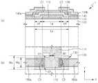
도 1은 본 발명의 제1 실시예에 따른 박막트랜지스터(1)를 개략적으로 도시한 도면이다.1 is a view schematically showing a
도 1의 (a)는 제1 실시예에 따른 박막트랜지스터(1)의 단면도이고, 도 1의 (b)는 제1 실시예에 따른 박막트랜지스터(1)의 평면도이다.1 (a) is a cross-sectional view of the
도 1을 참조하면, 제1 실시예에 따른 박막트랜지스터(1)는 기판(100) 상에 게이트 전극(110), 활성층(130) 및 소스 전극(150a)과 드레인 전극(150b)이 순차로 형성된 바텀(bottom) 게이트 구조이다.1, a
기판(100)은 SiO2를 주성분으로 하는 투명 재질의 글라스재로 형성될 수 있다. 물론 불투명 재질도 가능하며, 플라스틱재와 같은 다른 재질로 이루어질 수도 있다.The
기판(100) 상에는 기판(100)의 평활성과 불순 원소의 침투를 차단하기 위하여 SiO2 및/또는 SiNx 등을 포함하는 버퍼층(미도시)이 더 구비될 수 있다.A buffer layer (not shown) including SiO2 and / or SiNx may be further provided on the
게이트 전극(110)은 제1방향(X)으로 제1길이(Lg)를 가지고, 제2방향(Y)으로 제1폭(Wg)을 갖도록 형성된다. 즉, 게이트 전극(110)은 제1방향(X)으로 제1길이(Lg)를 갖는 양 측 경계와, 제2방향(Y)으로 제1폭(Wg)을 갖는 양 측 경계로 정의될 수 있다. 여기서, 게이트 전극(110)의 제1방향(X)으로의 제1길이(Lg)는 제2방향(Y)으로의 제1폭(Wg)보다 길게 형성된다.The
게이트 전극(110)의 제1방향(X)으로의 양 측 경계 중 하나는, 상기 게이트 전극(110)에 주사 신호를 인가하기 위한 배선(111)에 연결된다.One of the two side boundaries in the first direction X of the
본 실시예에서 상기 배선(111)은 상기 게이트 전극(110)의 제1길이(Lg)보다 작은 폭(W1)을 가지고, 상기 게이트 전극(110)에 제2방향(Y)으로 연장되어 배치된다. 상기 도면에는 게이트 전극(110)과 상기 배선(111)이 티(┬)자 형상으로 연결된 것으로 도시되어 있으나, 이는 일 예시이며 본 발명은 이에 한정되지 않는다.The
게이트 전극(110) 및 상기 게이트 전극(110)에 연장된 배선(111)은 Ag, Mg, Al, Pt, Pd, Au, Ni, Nd, Ir, Cr, Li, Ca, Mo, Ti, W, MoW, 및 Al/Cu 가운데 선택된 하나 이상의 도전성 물질이 사용될 수 있다.The
게이트 전극(110) 상에 상기 게이트 전극(110)을 덮도록 제1절연층(120)이 구비된다. 제1절연층(120)은 게이트 절연막으로 기능한다. 제1절연층(120)은 SiO2, SiNx, SiON, Al2O3, TiO2, Ta2O5, HfO2, 및 ZrO2 가운데 선택된 하나 이상의 무기 절연막이 사용될 수 있다.A first
제1절연층(120) 상에 산화물 반도체를 포함하는 활성층(130)이 구비된다. 산화물 반도체는 갈륨(Ga), 인듐(In), 아연(Zn), 하프늄(Hf) 및 주석(Sn) 군에서 선택된 하나 이상의 원소를 포함할 수 있다. 예를 들어, 활성층(130)은 InGaZnO, ZnSnO, InZnO, InGaO, ZnO, TiO, 및 HIZO(hafnium-indium-zinc oxide)에서 선택될 수 있다.An
본 실시예에서 활성층(130)은 제1방향(X)으로 제2길이(La)를 가지고, 제2방향(Y)으로 제2폭(Wa)을 갖도록 형성된다. 여기서, 활성층(130)의 제1방향(X)으로 제2길이(La)는 제2방향(Y)으로 제2폭(Wa)보다 길게 형성될 수 있다.The
활성층(130) 상에 층간 절연막인 제2절연층(140)이 구비된다. 제2절연층(140)은 SiO2, SiNx, SiON, Al2O3, TiO2, Ta2O5, HfO2, 및 ZrO2 가운데 선택된 하나 이상의 무기 절연막이 사용될 수 있다.A second
제2절연층(140) 상에는 상기 제2절연층(140)에 형성된 콘택홀(C1, C2)을 통하여 상기 활성층(130)에 각각 접속하는 소스 전극(150a)과 드레인 전극(150b)이 구비된다.A
소스 전극(150a)과 드레인 전극(150b)은 각각 제1방향(X)으로 연장되어 배치된다. 상기 도면에는 소스 전극(150a)과 드레인 전극(150b)의 제2방향(Y)으로의 폭이 게이트 전극(110)의 제2방향으로의 폭(Wg)보다 작게 도시되어 있으나, 이는 예시일 뿐 본 발명은 이에 한정되지 않는다.The
한편, 도 1에는 상세히 도시되어 있지 않으나, 활성층(130)의 외곽에는 n+ 타입 또는 p+ 타입의 이온 불순물이 도핑 된 영역이 형성될 수 있다. 이 경우, 전술한 콘택홀(C1, C2)은 소스 전극(150a)과 드레인 전극(150b)을 이온 불순물이 도핑된 영역에 접속시킬 수 있다.Although not shown in detail in FIG. 1, a region doped with n + type or p + type ion impurities may be formed on the outer side of the
활성층(130)과, 게이트 전극(110)과 상기 게이트 전극(110)에 연결된 배선(111)과 오버랩 되는 영역에 채널(channel)이 형성된다. 일반적인 박막트랜지스터는 게이트 전극(110)의 제1방향(X)으로의 제1길이(Lg)가 활성층(130)의 제2길이(La)보다 작고, 게이트 전극(110)의 제2방향(Y)으로의 제1폭(Wg)이 활성층(130)의 제2폭(Wa)보다 크게 형성된다.A channel is formed in an area overlapping the
그러나, 본 실시예에 따른 박막트랜지스터(1)는 전술하였듯이, 게이트 전극(110)의 제1방향(X)으로의 제1길이(Lg)가 활성층(130)의 제2길이(La)보다 작게 형성되고, 동시에 게이트 전극(110)의 제2방향(Y)으로의 제1폭(Wg)도 활성층(130)의 제2폭(Wa)보다 작게 형성된다.However, in the
더욱 상세하게는, 게이트 전극(110)의 제1방향(X)으로의 양 측 경계는 활성층(130)의 제1방향(X)으로의 양측 경계로부터 이격되어 상기 활성층(130)의 제1방향(X)의 경계로부터 ΔY만큼 이격되어 제1방향(X)으로의 양측 경계의 내부에 위치하고, 게이트 전극(110)의 제2방향(Y)으로의 양측 경계는 활성층(130)의 제2방향(Y)으로의 양측 경계로부터 ΔX만큼 이격되어 상기 활성층(130)의 제2방향(Y)으로의 양측 경계의 내부에 위치한다.More specifically, both side boundaries in the first direction X of the
또한, 게이트 전극(110)에 제2방향(Y)으로 연결된 배선(111)은, 활성층(130)의 제1방향(X)의 양측 경계 중 일측 경계에서 부분적으로 오버랩된다. 따라서, 상기 배선(111)과 활성층(130)은 채널의 제1방향(X)의 경계에서 상기 배선(111)의 폭(W1)만큼 오버랩된다.The
여기서, 채널의 경계에서 게이트 전극(110)과 연결되는 부분의 배선 폭(W1)은 채널의 경계와 오버랩되는 영역을 줄이기 위한 것이므로, 채널의 경계로부터 떨어진 곳에 위치하는 배선(111)의 폭은 채널의 경계에서 오버랩되는 배선 폭(W1)보다 더 넓게 형성될 수 있다. 도 1에는 채널의 경계로부터 떨어진 곳에 위치하는 배선(111)의 폭이 게이트 전극(110)의 제1방향(X)의 길이(Lg)와 동일하게 도시되어 있으나 이는 일 예시이며 이와 다른 폭을 가져도 무방하다.Since the width W1 of the portion connected to the
상술한 바와 같이, 본 실시예에 따른 박막트랜지스터(1)는 채널의 경계에서 게이트 전극(110) 및/또는 배선(11)과, 활성층(130)의 제1방향(X)의 경계에서 오버랩되는 부분이 작기 때문에, 드레인 전압에 따른 박막트랜지스터의 문턱전압(threshold voltage: Vth)의 변화가 거의 없어 안정적인 소자 특성을 구현할 수 있다.As described above, the
도 2는 본 발명의 제1 실시예에 따른 박막트랜지스터(1)의 드레인 전압(Vd)에 대한 게이트 전압(Vg)-드레인 전류(Id)의 관계를 나타낸 그래프이다.2 is a graph showing the relationship between the gate voltage Vg and the drain current Id versus the drain voltage Vd of the
도 2의 그래프는 게이트 전극(110)의 제1방향(X)으로의 제1길이(Lg)가 40㎛, 제2방향(Y)으로의 제1폭(Wg)이 20㎛이고, 게이트 전극(110)의 제1방향(X)으로의 양 측 경계가 활성층(130)의 제1방향(X)의 경계로부터 2㎛(=ΔY) 이격되고, 채널의 제1방향(X)의 경계에 오버랩되는 배선(111)의 폭(W1)이 4㎛인 박막트랜지스터에 대한 것이다.2, the first length Lg of the
여기서, G0는 바이어스 전압(VD=0.1V)에 대한 게이트 전압(Vg)-드레인 전류(Id)의 관계를 나타낸 것이고, G1는 드레인 전압(VD)이 5.1V 일 때 게이트 전압(Vg)-드레인 전류(Id)의 관계를 나타낸 것이다.G0 represents the relationship between the gate voltage Vg and the drain current Id with respect to the bias voltage VD = 0.1 V. G1 indicates the relationship between the gate voltage Vg and the drain current Id when the drain voltage VD is 5.1 V. [ And the current Id.
G0와 G1을 참조하면, 본 실시예에 따른 박막트랜지스터(1)는 드레인 전압을 증가시키더라도 박막트랜지스터의 문턱전압(threshold voltage: Vth)에 대한 변화가 거의 없음을 알 수 있다.Referring to G0 and G1, it can be seen that the threshold voltage (Vth) of the thin film transistor is almost unchanged even if the drain voltage is increased in the
드레인 전압을 증가시키면 채널의 경계에서 결함(defect)이 발생하여 박막트랜지스터의 문턱전압을 변화시킬 수 있는데, 본 실시예에 따른 박막트랜지스터는 게이트 전극(110)과 활성층(130)이 채널 경계에서 오버랩되는 부분을 줄임으로써 문턱전압의 변화가 거의 없는 안정적인 소자를 구현할 수 있다.The
한편, 이러한 결함은 채널의 길이가 폭보다 크게 형성되는 소자에서 더욱 뚜렷하게 증가하는 경향이 있다. 게이트 전극(110)의 제1방향(X)으로의 제1길이(Lg)가 제2방향(Y)으로의 제2폭(Wg)보다 길게 형성되는 박막트랜지스터에, 상술한 본 실시예에 따른 채널 경계에서 게이트 전극(110)과 오버랩되는 부분을 최소화한 구조를 적용시킬 때, 박막트랜지스터의 문턱전압의 변화를 최소화 할 수 있다.On the other hand, such defects tend to increase more markedly in the device in which the channel length is formed larger than the width. The first length Lg of the
도 3은 본 발명의 비교예에 따른 박막트랜지스터(2)를 개략적으로 도시한 평면도이다.3 is a plan view schematically showing a
도 3을 참조하면, 본 비교예에 따른 박막트랜지스터(2)는 게이트 전극(10), 활성층(30), 및 소스 전극(50a)과 드레인 전극(50b)을 구비한다.Referring to FIG. 3, the
본 비교예에서 활성층(30)은 전술한 실시예와 마찬가지로 제1방향(X)으로 제2길이(La)를 가지고, 제2방향(Y)으로 제2폭(Wa)을 갖도록 형성된다. 그러나, 본 비교예에 따른 게이트 전극(10)은 제1방향(X)으로는 활성층(30)의 제2길이(La)보다 작은 제1길이(Lg)를 가지지만, 제2방향(Y)으로는 활성층(30)의 제2폭(Wa)보다 큰 제1폭(Wg)을 갖는다.In this comparative example, the active layer 30 is formed to have a second length La in the first direction X and a second width Wa in the second direction Y, as in the above-described embodiment. However, the
즉, 게이트 전극(10)의 제1방향(X)으로의 양측 경계는 활성층(30)의 제1방향(X)으로의 양측 경계로부터 이격되어 활성층(30)의 제1방향(X)으로의 양측 경계 내부에 위치하지만, 게이트 전극(110)의 제2방향(Y)으로의 양 측 경계는 활성층(130)의 제2방향(Y)으로의 양측 경계와 오버랩되면서 활성층(30)의 제2방향(Y)으로의 양측 경계 외부에 위치한다. 즉, 상기 게이트 전극(10)과 활성층(30)은 채널의 제1방향(X)으로의 경계에서 상기 게이트 전극(10)의 제1방향(X)으로의 제1길이(Lg)만큼 오버랩된다.That is, the both side boundaries in the first direction X of the
따라서, 도 3의 비교예에 따른 박막트랜지스터(2)는 게이트 전극(10)과 활성층(30)은 도 1의 제1실시예에 따른 박막트랜지스터(1)에 비하여 채널의 경계에서 오버랩되는 부분이 증가하기 때문에, 드레인 전압에 따른 박막트랜지스터(2)의 문턱전압(Vth)의 변화로 안정적인 소자 특성을 구현할 수 없다.3, the
도 4는 도 3의 비교예에 따른 박막트랜지스터(2)의 드레인 전압(Vd)에 대한 게이트 전압(Vg)-드레인 전류(Id)의 관계를 나타낸 그래프이다.4 is a graph showing the relationship between the gate voltage Vg and the drain current Id versus the drain voltage Vd of the
도 4의 그래프는 게이트 전극(10)의 제1방향(X)으로의 제1길이(Lg)가 50㎛, 제2방향(Y)으로의 제1폭(Wg)이 25㎛이고, 채널의 제1방향(X)의 경계에 오버랩되는 배선(11)의 폭이 게이트 전극(10)의 제1길이(Lg)(=50㎛)과 같은 박막트랜지스터에 대한 것이다.4 shows that the first length Lg of the
여기서, G0는 바이어스 전압(VD=0.1V)에 대한 게이트 전압(Vg)-드레인 전류(Id)의 관계를 나타낸 것이고, G2는 드레인 전압(VD)이 5.1V 일 때 게이트 전압(Vg)-드레인 전류(Id)의 관계를 나타낸 것이다.G0 represents the relationship between the gate voltage Vg and the drain current Id with respect to the bias voltage VD = 0.1 V and G2 represents the relationship between the gate voltage Vg and the drain current Id when the drain voltage VD is 5.1 V. [ And the current Id.
G0와 G2를 참조하면, 본 비교예에 따른 박막트랜지스터(2)는 드레인 전압이 증가함에 따라 G2가 오른쪽으로 ΔV 만큼 시프트(shift) 되었음을 알 수 있다. 따라서, 본 비교예에 따른 박막트랜지스터(2)눈 채널의 경계에서 오버랩되는 부분이 증가하기 때문에, 드레인 전압에 따른 박막트랜지스터(2)의 문턱전압(Vth)의 변화로 안정적인 소자 특성을 구현할 수 없는 문제가 있다.
Referring to G0 and G2, it can be seen that G2 is shifted to the right by DELTA V as the drain voltage increases in the
도 5 내지 8은 본 발명의 다른 실시예에 따른 박막트랜지스터의 개략적인 구조를 도시한 단면도들이다.5 to 8 are cross-sectional views illustrating a schematic structure of a thin film transistor according to another embodiment of the present invention.
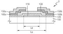
도 5는 본 발명의 제2 실시예에 따른 박막트랜지스터(3)를 개략적으로 도시한 단면도이다.5 is a cross-sectional view schematically showing a
도 5를 참조하면, 제2 실시예에 따른 박막트랜지스터(3)는 제1 실시예와 마찬가지로 기판(100) 상에 게이트 전극(110), 활성층(130) 및 소스 전극(150a)과 드레인 전극(150b)이 순차로 형성된 바텀(bottom) 게이트 구조이다. 다만, 제1 실시예와는 달리 소스 전극(150a)과 드레인 전극(150b)이 콘택홀(C1, C2, 도 1 참조)을 통하여 활성층(130)에 접속하는 것이 아니라, 활성층(130)과 소스/드레인 전극(150a, 150b) 사이에 오믹콘택층(160a, 160b)이 각각 구비된다.5, the
도 6은 본 발명의 제3 실시예에 따른 박막트랜지스터(4)를 개략적으로 도시한 단면도이다.6 is a cross-sectional view schematically showing a
도 6을 참조하면, 제3 실시예에 따른 박막트랜지스터(4)는 기판(100) 상에 활성층(130), 소스 전극(150a)과 드레인 전극(150b), 및 게이트 전극(110)이 순차로 형성된 탑(top) 게이트 구조이다. 소스 전극(150a)과 드레인 전극(150b)은 제1절연층(120)에 형성된 콘택홀(C1, C2)을 통하여 활성층(130)에 접속한다.6, the
도 7은 본 발명의 제4 실시예에 따른 박막트랜지스터(3)를 개략적으로 도시한 단면도이다.7 is a cross-sectional view schematically showing a
도 7을 참조하면, 제4 실시예에 따른 박막트랜지스터(5)는 전술한 제3실시예와 같이 기판(100) 상에 활성층(130), 소스 전극(150a)과 드레인 전극(150b), 및 게이트 전극(110)이 순차로 형성된 탑(top) 게이트 구조이다. 다만, 제3 실시예와는 달리 소스 전극(150a)과 드레인 전극(150b)이 콘택홀(C1, C2, 도 6 참조)을 통하여 활성층(130)에 접속하는 것이 아니라, 활성층(130)과 소스/드레인 전극(150a, 150b) 사이에 오믹콘택층(160a, 160b)이 각각 구비된다.7, the
도 8은 본 발명의 제5 실시예에 따른 박막트랜지스터(6)를 개략적으로 도시한 단면도이다.8 is a cross-sectional view schematically showing a
도 8을 참조하면, 제5 실시예에 따른 박막트랜지스터(3)는 기판(100) 상에 활성층(130), 게이트 전극(110), 및 소스 전극(150a)과 드레인 전극(150b)이 순차로 형성된 탑(top) 게이트 구조이다. 전술한 제1 실시예와 비교할 때, 게이트 전극(110)과 활성층(130)의 순서가 달라진 것이다.Referring to FIG. 8, the
상술한 도 5 내지 8의 실시예에 따른 박막트랜지스터들(3~6)은 게이트 전극(110)의 제1길이(Lg)가 활성층(130)의 제2길이(La)보다 짧은 것을 도시한 단면만 도시되어 있으나, 상기 실시예들은 전술한 제1 실시예와 마찬가지로 게이트 전극(110)의 제1폭(Wg)이 활성층(130)의 제2폭(Wa)보다 작게 형성된 것이다. 따라서, 채널의 경계에서 게이트 전극(110)과 오버랩되는 부분이 작아 드레인 전압에 따른 박막트랜지스터의 문턱전압(Vth)의 변화가 거의 없어 안정적인 소자 특성을 구현할 수 있다.The
한편, 도 5 내지 8에 도시된 박막트랜지스터들은 본 발명의 일 예시이며, 본 발명은 상술한 상기 도면에 한정되지 않고 더 다양한 구조의 박막트랜지스터에 적용될 수 있음은 물론이다.Meanwhile, the thin film transistors shown in FIGS. 5 to 8 are examples of the present invention, and the present invention is not limited to the above-described drawings, and it goes without saying that the present invention can be applied to thin film transistors having various structures.
도 9는 도 1의 박막트랜지스터가 포함된 유기 발광 표시 장치(7)를 개략적으로 도시한 단면도이다.9 is a cross-sectional view schematically showing an organic light emitting
도 9에 도시된 유기 발광 표시 장치(7)는 산화물 반도체를 포함하는 박막트랜지스터를 포함한다. 도 9에는 제1 실시예에 따른 박막트랜지스터(1)가 도시되어 있으나 본 발명은 이에 한정되지 않으며, 전술한 제2 내지 제5 실시예에 따른 박막트랜지스터(3~6)을 포함할 수 있음은 물론이다.The organic light emitting
본 실시예에 따른 유기 발광 표시 장치(7)는 기판(100) 상에 게이트 전극(110), 제1절연층(120), 활성층(130), 제2절연층(140) 및 소스 전극(150a)과 드레인 전극(150b)이 차례로 구비되고, 소스 전극(150a)과 드레인 전극(150b) 상에 제3절연층(180)이 형성된다. 여기서, 박막트랜지스터의 각 구성요소는 전술한 제1 실시예와 동일하므로 자세한 설명은 생략한다.The organic light emitting
제3절연층(180)에 형성된 콘택홀(C3)을 통하여 화소 전극(190)은 드레인 전극(150b)과 접속한다. 한편, 본 도 9는 소스 전극(150a)과 드레인 전극(150b) 중 하나가 화소 전극(190)에 직접 접속된 구동 박막트랜지스터)를 도시하고 있으나, 전술한 바와 같이 본 발명은 스위칭 박막트랜지스터에도 적용될 수 있음은 물론이다.The
화소 전극(190) 상에는 유기 발광층(210)이 형성되고, 유기 발광층(210) 상에는 공통 전극으로 대향 전극(220)이 형성된다. 본 실시예에 따른 유기 발광 표시 장치(7)의 경우, 화소 전극(190)은 애노드로 사용되고, 대향 전극(220)은 캐소드로 사용된다. 물론 전극의 극성은 반대로 적용될 수 있음은 물론이다.An organic
유기 발광층(210)은 저분자 유기물 또는 고분자 유기물일 수 있다. 유기 발광층(210)이 저분자 유기물일 경우, 유기 발광층(210)을 중심으로 홀 수송층(hole transport layer: HTL), 홀 주입층(hole injection layer: HIL), 전자 수송층(electron transport layer: ETL) 및 전자 주입층(electron injection layer: EIL) 등이 적층될 수 있다. 이외에도 필요에 따라 다양한 층들이 적층 될 수 있다. 이때, 사용 가능한 유기 재료로 구리 프탈로시아닌(CuPc: copper phthalocyanine), N'-디(나프탈렌-1-일)-N(N'-Di(naphthalene-1-yl)-N), N'-디페닐-벤지딘(N'-diphenyl-benzidine: NPB), 트리스-8-하이드록시퀴놀린 알루미늄(tris-8-hydroxyquinoline aluminum)(Alq3) 등을 비롯하여 다양하게 적용 가능하다. 한편, 유기 발광층(120)이 고분자 유기물일 경우, 유기 발광층(120) 외에 홀 수송층(HTL)이 포함될 수 있다. 홀 수송층은 폴리에틸렌 디히드록시티오펜 (PEDOT: poly-(3,4)-ethylene-dihydroxy thiophene)이나, 폴리아닐린(PANI: polyaniline) 등을 사용할 수 있다. 이때, 사용 가능한 유기 재료로 PPV(Poly-Phenylenevinylene)계 및 폴리플루오렌(Polyfluorene)계 등의 고분자 유기물을 사용할 수 있다.The organic
화소 전극(190)이 투명 전극으로 사용될 경우, 대향 전극(220)은 반사 전극으로 사용될 수 있다. 또한, 반대로 화소 전극(190)이 반사 전극으로, 대향 전극(220)이 투명 전극으로 사용될 수도 있다. 이와 같이 유기 발광층(210)에서 방출된 광은 투명 전극을 통하여 외부로 방출되어 영상을 표시한다.When the
한편, 도 9에는 도시되어 있지 않으나 대향 전극 상에는 상기 유기 발광층(210)을 외부의 산소와 수분으로부터 보호하는 봉지 부재(미도시)가 더 구비될 수 있다.Although not shown in FIG. 9, a sealing member (not shown) for protecting the organic
산화물 반도체를 포함하는 박막트랜지스터는 소자 특성이 우수하고 저온공정이 가능하여 평판 표시용 백플레인(backplane)에 최적인 소자로 평가되고 있다. 뿐만 아니라 산화물 반도체를 포함하는 박막트랜지스터는 가사광선 영역에서 투명한 특성을 가질 뿐 아니라 유연하기 때문에 투명 표시 장치나 플렉서블 표시 장치에도 적용될 수 있다. 또한, 전술한 바와 같이, 본 발명에 따른 산화물 반도체를 포함하는 박막트랜지스터는 드레인 전압에 따른 박막트랜지스터의 문턱전압(Vth)의 변화가 거의 없어 안정적인 소자 특성을 구현할 수 있어서, 평판 표시용 백플레인에 스위칭 트랜지스터 및/또는 구동 트랜지스터로 사용될 수 있다.Thin film transistors including oxide semiconductors are excellent in device characteristics and can be processed at a low temperature, and thus they are evaluated to be the most suitable for a backplane for flat panel display. In addition, a thin film transistor including an oxide semiconductor can be applied to a transparent display device or a flexible display device because it is transparent as well as transparent in the visible light region. In addition, as described above, since the thin film transistor including the oxide semiconductor according to the present invention hardly changes the threshold voltage (Vth) of the thin film transistor according to the drain voltage, stable device characteristics can be realized, Transistors and / or driving transistors.
한편, 유기 발광 표시 장치는 투명하고 유연하여 전술한 산화물 반도체를 포함하는 박막트랜지스터와 함께 투명 표시 장치나 플렉서블 표시 장치에 많이 활용되고 있다.On the other hand, the organic light emitting display device is transparent and flexible and is widely used in a transparent display device or a flexible display device together with a thin film transistor including the above-described oxide semiconductor.
상술한 설명들은 유기 발광 표시 장치를 중심으로 기술되었으나, 본 발명은 이에 한정되지 않는다. 예를 들어, 본 발명은 유기 발광층 대신에 액정이 구비된 액정 표시 장치에 적용될 수 있음은 물론이다. 이외 다른 표시 장치에도 적용될 수 있다.Although the above description has been made with reference to the organic light emitting diode display, the present invention is not limited thereto. For example, the present invention can be applied to a liquid crystal display having a liquid crystal instead of the organic light emitting layer. But may be applied to other display devices.
본 발명은 도면에 도시된 실시 예를 참고로 설명되었으나 이는 예시적인 것에 불과하며, 당해 기술 분야에서 통상의 지식을 가진 자라면 이로부터 다양한 변형 및 균등한 다른 실시 예가 가능하다는 점을 이해할 것이다. 따라서, 본 발명의 진정한 기술적 보호 범위는 첨부된 특허청구범위의 기술적 사상에 의하여 정해져야 할 것이다.While the present invention has been described with reference to exemplary embodiments, it is to be understood that the invention is not limited to the disclosed exemplary embodiments, but, on the contrary, is intended to cover various modifications and equivalent arrangements included within the spirit and scope of the invention. Accordingly, the true scope of the present invention should be determined by the technical idea of the appended claims.
1: 박막트랜지스터 100: 기판
110: 게이트 전극120: 제1 절연층
111: 배선130: 활성층
140: 제2 절연층150a: 소스 전극
150b: 드레인 전극Lg: 제1길이
Wg: 제1폭La: 제2길이
Wa: 제2폭C1~C3: 개구1: thin film transistor 100: substrate
110: gate electrode 120: first insulating layer
111: wiring 130: active layer
140: second insulating
150b: drain electrode Lg: first length
Wg: first width La: second length
Wa: second width C1 to C3: opening
Claims (16)
Translated fromKorean상기 제1방향으로 상기 게이트 전극의 제1길이 보다 긴 제2길이, 및 상기 제2방향으로 상기 게이트 전극의 제1폭보다 큰 제2폭을 갖는 활성층;
상기 활성층과 중첩된 영역에서 상기 제2방향으로 상기 게이트 전극과 연결되어 상기 활성층 외부로 연장된 배선; 및
상기 활성층에 접속하는 소스 전극과 드레인 전극;을 포함하고,
상기 게이트 전극의 상기 제1방향으로의 양측 경계 중 적어도 하나는 상기 활성층의 상기 제1방향으로의 경계와 이격되어 배치되고,
상기 활성층과 중첩된 영역에서 상기 배선의 상기 제1방향으로의 폭은, 상기 활성층 외부의 상기 배선의 상기 제1방향으로서의 폭 및 상기 게이트 전극의 제1길이보다 좁은, 박막트랜지스터.A gate electrode having a first length in a first direction and a first width in a second direction different from the first direction;
An active layer having a second length longer than the first length of the gate electrode in the first direction and a second width larger than the first width of the gate electrode in the second direction;
A wiring connected to the gate electrode in the second direction in a region overlapping with the active layer and extending to the outside of the active layer; And
And a source electrode and a drain electrode connected to the active layer,
At least one of the two side boundaries in the first direction of the gate electrode is disposed apart from a boundary in the first direction of the active layer,
The width of the wiring in the first direction in the region overlapping the active layer is narrower than the width of the wiring in the first direction outside the active layer and the first length of the gate electrode.
상기 게이트 전극의 상기 제1방향으로의 양측 경계는 상기 활성층의 상기 제1방향으로의 양측 경계와 이격되어 배치된 박막트랜지스터.The method according to claim 1,
And both side edges of the gate electrode in the first direction are spaced apart from both side edges of the active layer in the first direction.
상기 게이트 전극의 상기 제1방향으로의 양측 경계는 상기 활성층의 상기 제1방향으로의 양측 경계와 동일한 간격으로 이격되어 배치된 박막트랜지스터.3. The method of claim 2,
And both side edges of the gate electrode in the first direction are spaced apart at equal intervals from both sides of the active layer in the first direction.
상기 게이트 전극의 상기 제1방향으로의 양측 경계는 상기 활성층의 상기 제1방향으로의 양측 경계의 내부에 위치하는 박막트랜지스터3. The method of claim 2,
Wherein the gate electrode has a gate electrode and a gate electrode,
상기 게이트 전극의 상기 제1길이는 상기 제1폭보다 긴 박막트랜지스터.The method according to claim 1,
Wherein the first length of the gate electrode is longer than the first width.
상기 소스 전극과 드레인 전극은 상기 제1방향으로 마주보며 연장된 박막트랜지스터.The method according to claim 1,
Wherein the source electrode and the drain electrode extend in opposition to each other in the first direction.
상기 활성층은 산화물 반도체를 포함하는 박막트랜지스터.The method according to claim 1,
Wherein the active layer includes an oxide semiconductor.
상기 활성층은 갈륨(Ga), 인듐(In), 아연(Zn), 하프늄(Hf) 및 주석(Sn) 군에서 선택된 하나 이상의 원소와, 산소(O)를 포함하는 박막트랜지스터.9. The method of claim 8,
Wherein the active layer comprises at least one element selected from the group consisting of gallium (Ga), indium (In), zinc (Zn), hafnium (Hf), and tin (Sn) and oxygen (O).
상기 소스 전극과 드레인 전극은 각각 콘택홀을 통하여 상기 활성층에 접속하는 박막트랜지스터.The method according to claim 1,
Wherein the source electrode and the drain electrode are connected to the active layer through a contact hole, respectively.
상기 활성층은 이온 불순물이 도핑된 영역을 포함하고, 상기 소스 전극과 드레인 전극은 상기 콘택홀을 통하여 상기 도핑된 영역에 접속하는 박막트랜지스터.11. The method of claim 10,
Wherein the active layer includes a region doped with an ion impurity, and the source electrode and the drain electrode are connected to the doped region through the contact hole.
상기 소스 전극과 드레인 전극은 각각 오믹콘택층을 통하여 상기 활성층에 접속하는 박막트랜지스터.The method according to claim 1,
And the source electrode and the drain electrode are connected to the active layer through the ohmic contact layer, respectively.
상기 게이트 전극은 상기 활성층 아래에 배치된 박막트랜지스터.The method according to claim 1,
And the gate electrode is disposed under the active layer.
상기 게이트 전극은 상기 활성층 위에 배치된 박막트랜지스터.The method according to claim 1,
And the gate electrode is disposed on the active layer.
상기 박막트랜지스터에 의해 구동되는 표시 소자를 구비한 표시 장치.A gate electrode having a first length in a first direction and a first width in a second direction different from the first direction, a second length longer than a first length of the gate electrode in the first direction, An active layer having a second width larger than a first width of the gate electrode in two directions; a wiring connected to the gate electrode in the second direction in a region overlapping the active layer and extending to the outside of the active layer; Wherein at least one of both sides of the gate electrode in the first direction is disposed apart from a boundary of the active layer in the first direction and a region overlapping with the active layer in a region overlapping the active layer Wherein a width of the wiring in the first direction is narrower than a width of the wiring in the first direction outside the active layer and a first length of the gate electrode; And
And a display element driven by the thin film transistor.
상기 박막트랜지스터의 상기 소스 전극과 드레인 전극 중 하나와 연결된 화소 전극;
상기 화소 전극에 대향 배치된 대향 전극; 및
상기 화소 전극과 대향 전극 사이에 배치된 유기 발광층;을 포함하는 유기 발광 표시 장치.A gate electrode having a first length in a first direction and a first width in a second direction different from the first direction, a second length longer than a first length of the gate electrode in the first direction, An active layer having a second width larger than a first width of the gate electrode in two directions; a wiring connected to the gate electrode in the second direction in a region overlapping the active layer and extending to the outside of the active layer; Wherein at least one of both sides of the gate electrode in the first direction is disposed apart from a boundary of the active layer in the first direction and a region overlapping with the active layer in a region overlapping the active layer Wherein a width of the wiring in the first direction is narrower than a width of the wiring in the first direction outside the active layer and a first length of the gate electrode;
A pixel electrode connected to one of the source electrode and the drain electrode of the thin film transistor;
A counter electrode disposed opposite to the pixel electrode; And
And an organic light emitting layer disposed between the pixel electrode and the counter electrode.
Priority Applications (4)
| Application Number | Priority Date | Filing Date | Title |
|---|---|---|---|
| KR1020120026602AKR101951260B1 (en) | 2012-03-15 | 2012-03-15 | Thin Film Transistor, display apparatus comprising the thin film transistor, and organic light emitting display apparatus comprising the thin film transistor |
| US13/688,313US8723170B2 (en) | 2012-03-15 | 2012-11-29 | TFT, display apparatus including TFT, and organic light-emitting display apparatus including TFT |
| TW101145573ATWI581437B (en) | 2012-03-15 | 2012-12-05 | Thin film transistor, display device including thin film transistor, and organic light emitting display device including thin film transistor |
| CN201310009071.3ACN103311309B (en) | 2012-03-15 | 2013-01-10 | Thin film transistor (TFT), display device and oganic light-emitting display device |
Applications Claiming Priority (1)
| Application Number | Priority Date | Filing Date | Title |
|---|---|---|---|
| KR1020120026602AKR101951260B1 (en) | 2012-03-15 | 2012-03-15 | Thin Film Transistor, display apparatus comprising the thin film transistor, and organic light emitting display apparatus comprising the thin film transistor |
Publications (2)
| Publication Number | Publication Date |
|---|---|
| KR20130104770A KR20130104770A (en) | 2013-09-25 |
| KR101951260B1true KR101951260B1 (en) | 2019-02-25 |
Family
ID=49136321
Family Applications (1)
| Application Number | Title | Priority Date | Filing Date |
|---|---|---|---|
| KR1020120026602AActiveKR101951260B1 (en) | 2012-03-15 | 2012-03-15 | Thin Film Transistor, display apparatus comprising the thin film transistor, and organic light emitting display apparatus comprising the thin film transistor |
Country Status (4)
| Country | Link |
|---|---|
| US (1) | US8723170B2 (en) |
| KR (1) | KR101951260B1 (en) |
| CN (1) | CN103311309B (en) |
| TW (1) | TWI581437B (en) |
Families Citing this family (9)
| Publication number | Priority date | Publication date | Assignee | Title |
|---|---|---|---|---|
| KR102091663B1 (en)* | 2013-06-28 | 2020-03-23 | 삼성디스플레이 주식회사 | Thin film transistor and organic light emitting diode display |
| CN103545378B (en)* | 2013-11-05 | 2016-09-07 | 京东方科技集团股份有限公司 | Oxide thin film transistor and preparation method thereof, array base palte, display device |
| CN104376813B (en)* | 2013-11-26 | 2017-09-08 | 苹果公司 | Display picture element unit |
| US9647048B2 (en) | 2013-11-26 | 2017-05-09 | Apple Inc. | Capacitor structures for display pixel threshold voltage compensation circuits |
| US10283645B2 (en)* | 2015-07-27 | 2019-05-07 | Sharp Kabushiki Kaisha | Semiconductor device and method for manufacturing same |
| WO2018150962A1 (en)* | 2017-02-15 | 2018-08-23 | シャープ株式会社 | Active matrix substrate |
| CN107403841A (en)* | 2017-07-27 | 2017-11-28 | 武汉华星光电半导体显示技术有限公司 | Low-temperature polysilicon film transistor and preparation method thereof, display device |
| CN109920922B (en)* | 2017-12-12 | 2020-07-17 | 京东方科技集团股份有限公司 | Organic light-emitting device, preparation method thereof, display substrate and display driving method |
| KR102859780B1 (en)* | 2019-12-10 | 2025-09-15 | 삼성디스플레이 주식회사 | Light emitting element and display device comprising the same |
Citations (1)
| Publication number | Priority date | Publication date | Assignee | Title |
|---|---|---|---|---|
| JP2011071440A (en)* | 2009-09-28 | 2011-04-07 | Hitachi Displays Ltd | Organic el display device |
Family Cites Families (15)
| Publication number | Priority date | Publication date | Assignee | Title |
|---|---|---|---|---|
| US6316808B1 (en) | 1998-08-07 | 2001-11-13 | International Business Machines Corporation | T-Gate transistor with improved SOI body contact structure |
| JP3420201B2 (en)* | 1999-12-22 | 2003-06-23 | 日本電気株式会社 | Liquid crystal display |
| JP3522216B2 (en)* | 2000-12-19 | 2004-04-26 | シャープ株式会社 | Thin film transistor, method of manufacturing the same, and liquid crystal display |
| KR101034744B1 (en)* | 2004-06-25 | 2011-05-17 | 엘지디스플레이 주식회사 | Thin film transistor structure of liquid crystal display device |
| KR101087993B1 (en)* | 2005-11-02 | 2011-12-01 | 엘지디스플레이 주식회사 | Polycrystalline Silicon Thin Film Transistor |
| TWI336945B (en)* | 2006-06-15 | 2011-02-01 | Au Optronics Corp | Dual-gate transistor and pixel structure using the same |
| KR20080030799A (en)* | 2006-10-02 | 2008-04-07 | 삼성전자주식회사 | Thin film transistor substrate |
| KR101410926B1 (en)* | 2007-02-16 | 2014-06-24 | 삼성전자주식회사 | Thin film transistor and manufacturing method thereof |
| KR20080114262A (en) | 2007-06-27 | 2008-12-31 | 엘지전자 주식회사 | Thin film transistor and display device including same |
| KR100973642B1 (en) | 2008-04-21 | 2010-08-02 | 광주과학기술원 | Method of forming bottom gate type zinc oxide thin film transistor |
| US8247276B2 (en)* | 2009-02-20 | 2012-08-21 | Semiconductor Energy Laboratory Co., Ltd. | Thin film transistor, method for manufacturing the same, and semiconductor device |
| US9312156B2 (en) | 2009-03-27 | 2016-04-12 | Semiconductor Energy Laboratory Co., Ltd. | Thin film transistor |
| JP5532803B2 (en)* | 2009-09-30 | 2014-06-25 | ソニー株式会社 | Semiconductor device and display device |
| JPWO2011043300A1 (en)* | 2009-10-09 | 2013-03-04 | シャープ株式会社 | Semiconductor device and manufacturing method thereof |
| US9012904B2 (en)* | 2011-03-25 | 2015-04-21 | Semiconductor Energy Laboratory Co., Ltd. | Semiconductor device and method for manufacturing the same |
- 2012
- 2012-03-15KRKR1020120026602Apatent/KR101951260B1/enactiveActive
- 2012-11-29USUS13/688,313patent/US8723170B2/enactiveActive
- 2012-12-05TWTW101145573Apatent/TWI581437B/enactive
- 2013
- 2013-01-10CNCN201310009071.3Apatent/CN103311309B/enactiveActive
Patent Citations (1)
| Publication number | Priority date | Publication date | Assignee | Title |
|---|---|---|---|---|
| JP2011071440A (en)* | 2009-09-28 | 2011-04-07 | Hitachi Displays Ltd | Organic el display device |
Also Published As
| Publication number | Publication date |
|---|---|
| TWI581437B (en) | 2017-05-01 |
| TW201338172A (en) | 2013-09-16 |
| CN103311309B (en) | 2017-08-25 |
| US20130240846A1 (en) | 2013-09-19 |
| KR20130104770A (en) | 2013-09-25 |
| US8723170B2 (en) | 2014-05-13 |
| CN103311309A (en) | 2013-09-18 |
Similar Documents
| Publication | Publication Date | Title |
|---|---|---|
| KR101951260B1 (en) | Thin Film Transistor, display apparatus comprising the thin film transistor, and organic light emitting display apparatus comprising the thin film transistor | |
| US11937456B2 (en) | Display apparatus | |
| US10580800B2 (en) | Thin film transistor and organic light emitting diode display including the same | |
| KR101108176B1 (en) | Double gate type thin film transistor and organic light emitting display device having same | |
| KR101885329B1 (en) | Substrate comprising thin film transistors and organic light emitting display apparatus comprising the same | |
| KR101912406B1 (en) | Backplane for flat panel display apparatus, the method of manufacturing for the backplane, and organic light emitting display apparatus comprising the backplane | |
| KR101842538B1 (en) | Backplane for flat panel display apparatus, flat panel display apparatus comprising the same, and manufacturing method of the backplane for flat panel display apparatus | |
| KR101074809B1 (en) | Organic light emitting display apparatus | |
| US10224435B2 (en) | Transistor, manufacturing method thereof, and display device including the same | |
| KR20180069974A (en) | Transistor array panel and display device including the same | |
| KR20130016938A (en) | Organic light emitting display device and manufacturing method of the same | |
| KR20160081100A (en) | Manufacturing method for organic light-emitting display apparatus and the Organic light-emitting display apparatus manufactured by the same method | |
| US20220093804A1 (en) | Thin film transistor array panel | |
| US9502574B2 (en) | Thin film transistor and manufacturing method thereof | |
| KR20150017193A (en) | Organic light emitting diode display | |
| US20140312315A1 (en) | Back plane of flat panel display and method of manufacturing the same | |
| US12408511B2 (en) | Thin-film transistor substrate and display apparatus including the same | |
| KR20220148993A (en) | Display Apparatus | |
| KR20150016785A (en) | Thin film transistor device and organic light emitting display including the same |
Legal Events
| Date | Code | Title | Description |
|---|---|---|---|
| PA0109 | Patent application | Patent event code:PA01091R01D Comment text:Patent Application Patent event date:20120315 | |
| N231 | Notification of change of applicant | ||
| PN2301 | Change of applicant | Patent event date:20120725 Comment text:Notification of Change of Applicant Patent event code:PN23011R01D | |
| PG1501 | Laying open of application | ||
| PA0201 | Request for examination | Patent event code:PA02012R01D Patent event date:20170131 Comment text:Request for Examination of Application Patent event code:PA02011R01I Patent event date:20120315 Comment text:Patent Application | |
| PE0902 | Notice of grounds for rejection | Comment text:Notification of reason for refusal Patent event date:20180511 Patent event code:PE09021S01D | |
| E701 | Decision to grant or registration of patent right | ||
| PE0701 | Decision of registration | Patent event code:PE07011S01D Comment text:Decision to Grant Registration Patent event date:20181120 | |
| GRNT | Written decision to grant | ||
| PR0701 | Registration of establishment | Comment text:Registration of Establishment Patent event date:20190218 Patent event code:PR07011E01D | |
| PR1002 | Payment of registration fee | Payment date:20190219 End annual number:3 Start annual number:1 | |
| PG1601 | Publication of registration | ||
| PR1001 | Payment of annual fee | Payment date:20220127 Start annual number:4 End annual number:4 | |
| PR1001 | Payment of annual fee | Payment date:20230125 Start annual number:5 End annual number:5 | |
| PR1001 | Payment of annual fee | Payment date:20240125 Start annual number:6 End annual number:6 |