KR101950349B1 - Method for gapfilling void―free polysilicon and mehto for fabricating semiconductor device using the same - Google Patents
Method for gapfilling void―free polysilicon and mehto for fabricating semiconductor device using the sameDownload PDFInfo
- Publication number
- KR101950349B1 KR101950349B1KR1020120153822AKR20120153822AKR101950349B1KR 101950349 B1KR101950349 B1KR 101950349B1KR 1020120153822 AKR1020120153822 AKR 1020120153822AKR 20120153822 AKR20120153822 AKR 20120153822AKR 101950349 B1KR101950349 B1KR 101950349B1
- Authority
- KR
- South Korea
- Prior art keywords
- forming
- layer
- contact plug
- air gap
- registration fee
- Prior art date
- Legal status (The legal status is an assumption and is not a legal conclusion. Google has not performed a legal analysis and makes no representation as to the accuracy of the status listed.)
- Active
Links
- 229910021420polycrystalline siliconInorganic materials0.000titleclaimsabstractdescription77
- 229920005591polysiliconPolymers0.000titleclaimsabstractdescription77
- 238000000034methodMethods0.000titleclaimsabstractdescription76
- 239000004065semiconductorSubstances0.000titleclaimsabstractdescription32
- 125000006850spacer groupChemical group0.000claimsabstractdescription71
- 239000000758substrateSubstances0.000claimsabstractdescription39
- 238000005530etchingMethods0.000claimsabstractdescription17
- 229910052751metalInorganic materials0.000claimsdescription47
- 239000002184metalSubstances0.000claimsdescription47
- 238000003860storageMethods0.000claimsdescription38
- NRTOMJZYCJJWKI-UHFFFAOYSA-NTitanium nitrideChemical compound[Ti]#NNRTOMJZYCJJWKI-UHFFFAOYSA-N0.000claimsdescription26
- VYPSYNLAJGMNEJ-UHFFFAOYSA-NSilicium dioxideChemical compoundO=[Si]=OVYPSYNLAJGMNEJ-UHFFFAOYSA-N0.000claimsdescription22
- 229910052814silicon oxideInorganic materials0.000claimsdescription22
- 239000000463materialSubstances0.000claimsdescription16
- 229910052582BNInorganic materials0.000claimsdescription9
- PZNSFCLAULLKQX-UHFFFAOYSA-NBoron nitrideChemical compoundN#BPZNSFCLAULLKQX-UHFFFAOYSA-N0.000claimsdescription9
- 239000003292glueSubstances0.000claims1
- 238000004519manufacturing processMethods0.000abstractdescription7
- 239000010410layerSubstances0.000description228
- 229910052581Si3N4Inorganic materials0.000description24
- HQVNEWCFYHHQES-UHFFFAOYSA-Nsilicon nitrideChemical compoundN12[Si]34N5[Si]62N3[Si]51N64HQVNEWCFYHHQES-UHFFFAOYSA-N0.000description24
- WFKWXMTUELFFGS-UHFFFAOYSA-NtungstenChemical compound[W]WFKWXMTUELFFGS-UHFFFAOYSA-N0.000description18
- 229910052721tungstenInorganic materials0.000description18
- 239000010937tungstenSubstances0.000description18
- 229910021332silicideInorganic materials0.000description16
- FVBUAEGBCNSCDD-UHFFFAOYSA-Nsilicide(4-)Chemical compound[Si-4]FVBUAEGBCNSCDD-UHFFFAOYSA-N0.000description16
- 230000004888barrier functionEffects0.000description14
- 238000007789sealingMethods0.000description14
- XUIMIQQOPSSXEZ-UHFFFAOYSA-NSiliconChemical compound[Si]XUIMIQQOPSSXEZ-UHFFFAOYSA-N0.000description13
- 239000010936titaniumSubstances0.000description13
- 238000002955isolationMethods0.000description12
- 229910052710siliconInorganic materials0.000description11
- 239000010703siliconSubstances0.000description11
- 229910052719titaniumInorganic materials0.000description11
- RTAQQCXQSZGOHL-UHFFFAOYSA-NTitaniumChemical compound[Ti]RTAQQCXQSZGOHL-UHFFFAOYSA-N0.000description10
- 239000000126substanceSubstances0.000description10
- 239000011800void materialSubstances0.000description9
- 239000011810insulating materialSubstances0.000description8
- MZLGASXMSKOWSE-UHFFFAOYSA-Ntantalum nitrideChemical compound[Ta]#NMZLGASXMSKOWSE-UHFFFAOYSA-N0.000description8
- 239000011229interlayerSubstances0.000description7
- 238000010030laminatingMethods0.000description7
- 239000010941cobaltSubstances0.000description6
- 229910017052cobaltInorganic materials0.000description6
- GUTLYIVDDKVIGB-UHFFFAOYSA-Ncobalt atomChemical compound[Co]GUTLYIVDDKVIGB-UHFFFAOYSA-N0.000description6
- 230000000052comparative effectEffects0.000description6
- KRHYYFGTRYWZRS-UHFFFAOYSA-NFluoraneChemical compoundFKRHYYFGTRYWZRS-UHFFFAOYSA-N0.000description4
- QAOWNCQODCNURD-UHFFFAOYSA-NSulfuric acidChemical compoundOS(O)(=O)=OQAOWNCQODCNURD-UHFFFAOYSA-N0.000description4
- IVHJCRXBQPGLOV-UHFFFAOYSA-NazanylidynetungstenChemical compound[W]#NIVHJCRXBQPGLOV-UHFFFAOYSA-N0.000description4
- 238000010586diagramMethods0.000description4
- 230000000694effectsEffects0.000description4
- 230000015572biosynthetic processEffects0.000description3
- 239000003990capacitorSubstances0.000description3
- 238000010438heat treatmentMethods0.000description3
- 150000004767nitridesChemical class0.000description3
- 229910019001CoSiInorganic materials0.000description2
- 206010010144Completed suicideDiseases0.000description2
- 229910019142PO4Inorganic materials0.000description2
- 229910000577Silicon-germaniumInorganic materials0.000description2
- LEVVHYCKPQWKOP-UHFFFAOYSA-N[Si].[Ge]Chemical compound[Si].[Ge]LEVVHYCKPQWKOP-UHFFFAOYSA-N0.000description2
- 238000000137annealingMethods0.000description2
- 238000004140cleaningMethods0.000description2
- 239000004020conductorSubstances0.000description2
- 238000000151depositionMethods0.000description2
- 230000008021depositionEffects0.000description2
- 230000009977dual effectEffects0.000description2
- 238000005468ion implantationMethods0.000description2
- 239000007769metal materialSubstances0.000description2
- 229910021421monocrystalline siliconInorganic materials0.000description2
- 230000003071parasitic effectEffects0.000description2
- NBIIXXVUZAFLBC-UHFFFAOYSA-KphosphateChemical compound[O-]P([O-])([O-])=ONBIIXXVUZAFLBC-UHFFFAOYSA-K0.000description2
- 239000010452phosphateSubstances0.000description2
- 229920000642polymerPolymers0.000description2
- 229910052715tantalumInorganic materials0.000description2
- GUVRBAGPIYLISA-UHFFFAOYSA-Ntantalum atomChemical compound[Ta]GUVRBAGPIYLISA-UHFFFAOYSA-N0.000description2
- 229910004298SiO 2Inorganic materials0.000description1
- 230000002159abnormal effectEffects0.000description1
- 238000005229chemical vapour depositionMethods0.000description1
- 239000013078crystalSubstances0.000description1
- 238000013500data storageMethods0.000description1
- 238000005516engineering processMethods0.000description1
- 238000009413insulationMethods0.000description1
- 239000012212insulatorSubstances0.000description1
- -1metal nitrideChemical class0.000description1
- 238000012986modificationMethods0.000description1
- 230000004048modificationEffects0.000description1
- 238000010079rubber tappingMethods0.000description1
- 239000007787solidSubstances0.000description1
- 230000003068static effectEffects0.000description1
- 150000003608titaniumChemical class0.000description1
- XLYOFNOQVPJJNP-UHFFFAOYSA-NwaterChemical compoundOXLYOFNOQVPJJNP-UHFFFAOYSA-N0.000description1
Images


Classifications
- H—ELECTRICITY
- H10—SEMICONDUCTOR DEVICES; ELECTRIC SOLID-STATE DEVICES NOT OTHERWISE PROVIDED FOR
- H10B—ELECTRONIC MEMORY DEVICES
- H10B12/00—Dynamic random access memory [DRAM] devices
- H—ELECTRICITY
- H01—ELECTRIC ELEMENTS
- H01L—SEMICONDUCTOR DEVICES NOT COVERED BY CLASS H10
- H01L21/00—Processes or apparatus adapted for the manufacture or treatment of semiconductor or solid state devices or of parts thereof
- H01L21/70—Manufacture or treatment of devices consisting of a plurality of solid state components formed in or on a common substrate or of parts thereof; Manufacture of integrated circuit devices or of parts thereof
- H01L21/71—Manufacture of specific parts of devices defined in group H01L21/70
- H01L21/768—Applying interconnections to be used for carrying current between separate components within a device comprising conductors and dielectrics
- H01L21/76897—Formation of self-aligned vias or contact plugs, i.e. involving a lithographically uncritical step
- H—ELECTRICITY
- H01—ELECTRIC ELEMENTS
- H01L—SEMICONDUCTOR DEVICES NOT COVERED BY CLASS H10
- H01L21/00—Processes or apparatus adapted for the manufacture or treatment of semiconductor or solid state devices or of parts thereof
- H01L21/02—Manufacture or treatment of semiconductor devices or of parts thereof
- H01L21/04—Manufacture or treatment of semiconductor devices or of parts thereof the devices having potential barriers, e.g. a PN junction, depletion layer or carrier concentration layer
- H01L21/18—Manufacture or treatment of semiconductor devices or of parts thereof the devices having potential barriers, e.g. a PN junction, depletion layer or carrier concentration layer the devices having semiconductor bodies comprising elements of Group IV of the Periodic Table or AIIIBV compounds with or without impurities, e.g. doping materials
- H01L21/28—Manufacture of electrodes on semiconductor bodies using processes or apparatus not provided for in groups H01L21/20 - H01L21/268
- H01L21/28008—Making conductor-insulator-semiconductor electrodes
- H01L21/28017—Making conductor-insulator-semiconductor electrodes the insulator being formed after the semiconductor body, the semiconductor being silicon
- H01L21/28026—Making conductor-insulator-semiconductor electrodes the insulator being formed after the semiconductor body, the semiconductor being silicon characterised by the conductor
- H01L21/28079—Making conductor-insulator-semiconductor electrodes the insulator being formed after the semiconductor body, the semiconductor being silicon characterised by the conductor the final conductor layer next to the insulator being a single metal, e.g. Ta, W, Mo, Al
- H—ELECTRICITY
- H01—ELECTRIC ELEMENTS
- H01L—SEMICONDUCTOR DEVICES NOT COVERED BY CLASS H10
- H01L21/00—Processes or apparatus adapted for the manufacture or treatment of semiconductor or solid state devices or of parts thereof
- H01L21/02—Manufacture or treatment of semiconductor devices or of parts thereof
- H01L21/04—Manufacture or treatment of semiconductor devices or of parts thereof the devices having potential barriers, e.g. a PN junction, depletion layer or carrier concentration layer
- H01L21/18—Manufacture or treatment of semiconductor devices or of parts thereof the devices having potential barriers, e.g. a PN junction, depletion layer or carrier concentration layer the devices having semiconductor bodies comprising elements of Group IV of the Periodic Table or AIIIBV compounds with or without impurities, e.g. doping materials
- H01L21/28—Manufacture of electrodes on semiconductor bodies using processes or apparatus not provided for in groups H01L21/20 - H01L21/268
- H01L21/28008—Making conductor-insulator-semiconductor electrodes
- H01L21/28017—Making conductor-insulator-semiconductor electrodes the insulator being formed after the semiconductor body, the semiconductor being silicon
- H01L21/28026—Making conductor-insulator-semiconductor electrodes the insulator being formed after the semiconductor body, the semiconductor being silicon characterised by the conductor
- H01L21/28088—Making conductor-insulator-semiconductor electrodes the insulator being formed after the semiconductor body, the semiconductor being silicon characterised by the conductor the final conductor layer next to the insulator being a composite, e.g. TiN
- H—ELECTRICITY
- H01—ELECTRIC ELEMENTS
- H01L—SEMICONDUCTOR DEVICES NOT COVERED BY CLASS H10
- H01L21/00—Processes or apparatus adapted for the manufacture or treatment of semiconductor or solid state devices or of parts thereof
- H01L21/02—Manufacture or treatment of semiconductor devices or of parts thereof
- H01L21/04—Manufacture or treatment of semiconductor devices or of parts thereof the devices having potential barriers, e.g. a PN junction, depletion layer or carrier concentration layer
- H01L21/18—Manufacture or treatment of semiconductor devices or of parts thereof the devices having potential barriers, e.g. a PN junction, depletion layer or carrier concentration layer the devices having semiconductor bodies comprising elements of Group IV of the Periodic Table or AIIIBV compounds with or without impurities, e.g. doping materials
- H01L21/30—Treatment of semiconductor bodies using processes or apparatus not provided for in groups H01L21/20 - H01L21/26
- H01L21/31—Treatment of semiconductor bodies using processes or apparatus not provided for in groups H01L21/20 - H01L21/26 to form insulating layers thereon, e.g. for masking or by using photolithographic techniques; After treatment of these layers; Selection of materials for these layers
- H01L21/3105—After-treatment
- H01L21/311—Etching the insulating layers by chemical or physical means
- H01L21/31105—Etching inorganic layers
- H01L21/31111—Etching inorganic layers by chemical means
- H01L21/31116—Etching inorganic layers by chemical means by dry-etching
- H—ELECTRICITY
- H01—ELECTRIC ELEMENTS
- H01L—SEMICONDUCTOR DEVICES NOT COVERED BY CLASS H10
- H01L21/00—Processes or apparatus adapted for the manufacture or treatment of semiconductor or solid state devices or of parts thereof
- H01L21/02—Manufacture or treatment of semiconductor devices or of parts thereof
- H01L21/04—Manufacture or treatment of semiconductor devices or of parts thereof the devices having potential barriers, e.g. a PN junction, depletion layer or carrier concentration layer
- H01L21/18—Manufacture or treatment of semiconductor devices or of parts thereof the devices having potential barriers, e.g. a PN junction, depletion layer or carrier concentration layer the devices having semiconductor bodies comprising elements of Group IV of the Periodic Table or AIIIBV compounds with or without impurities, e.g. doping materials
- H01L21/30—Treatment of semiconductor bodies using processes or apparatus not provided for in groups H01L21/20 - H01L21/26
- H01L21/31—Treatment of semiconductor bodies using processes or apparatus not provided for in groups H01L21/20 - H01L21/26 to form insulating layers thereon, e.g. for masking or by using photolithographic techniques; After treatment of these layers; Selection of materials for these layers
- H01L21/3105—After-treatment
- H01L21/311—Etching the insulating layers by chemical or physical means
- H01L21/31144—Etching the insulating layers by chemical or physical means using masks
- H—ELECTRICITY
- H01—ELECTRIC ELEMENTS
- H01L—SEMICONDUCTOR DEVICES NOT COVERED BY CLASS H10
- H01L21/00—Processes or apparatus adapted for the manufacture or treatment of semiconductor or solid state devices or of parts thereof
- H01L21/02—Manufacture or treatment of semiconductor devices or of parts thereof
- H01L21/04—Manufacture or treatment of semiconductor devices or of parts thereof the devices having potential barriers, e.g. a PN junction, depletion layer or carrier concentration layer
- H01L21/18—Manufacture or treatment of semiconductor devices or of parts thereof the devices having potential barriers, e.g. a PN junction, depletion layer or carrier concentration layer the devices having semiconductor bodies comprising elements of Group IV of the Periodic Table or AIIIBV compounds with or without impurities, e.g. doping materials
- H01L21/30—Treatment of semiconductor bodies using processes or apparatus not provided for in groups H01L21/20 - H01L21/26
- H01L21/324—Thermal treatment for modifying the properties of semiconductor bodies, e.g. annealing, sintering
- H—ELECTRICITY
- H01—ELECTRIC ELEMENTS
- H01L—SEMICONDUCTOR DEVICES NOT COVERED BY CLASS H10
- H01L21/00—Processes or apparatus adapted for the manufacture or treatment of semiconductor or solid state devices or of parts thereof
- H01L21/70—Manufacture or treatment of devices consisting of a plurality of solid state components formed in or on a common substrate or of parts thereof; Manufacture of integrated circuit devices or of parts thereof
- H01L21/71—Manufacture of specific parts of devices defined in group H01L21/70
- H01L21/768—Applying interconnections to be used for carrying current between separate components within a device comprising conductors and dielectrics
- H01L21/76801—Applying interconnections to be used for carrying current between separate components within a device comprising conductors and dielectrics characterised by the formation and the after-treatment of the dielectrics, e.g. smoothing
- H01L21/76802—Applying interconnections to be used for carrying current between separate components within a device comprising conductors and dielectrics characterised by the formation and the after-treatment of the dielectrics, e.g. smoothing by forming openings in dielectrics
- H—ELECTRICITY
- H01—ELECTRIC ELEMENTS
- H01L—SEMICONDUCTOR DEVICES NOT COVERED BY CLASS H10
- H01L21/00—Processes or apparatus adapted for the manufacture or treatment of semiconductor or solid state devices or of parts thereof
- H01L21/70—Manufacture or treatment of devices consisting of a plurality of solid state components formed in or on a common substrate or of parts thereof; Manufacture of integrated circuit devices or of parts thereof
- H01L21/71—Manufacture of specific parts of devices defined in group H01L21/70
- H01L21/768—Applying interconnections to be used for carrying current between separate components within a device comprising conductors and dielectrics
- H01L21/76801—Applying interconnections to be used for carrying current between separate components within a device comprising conductors and dielectrics characterised by the formation and the after-treatment of the dielectrics, e.g. smoothing
- H01L21/7682—Applying interconnections to be used for carrying current between separate components within a device comprising conductors and dielectrics characterised by the formation and the after-treatment of the dielectrics, e.g. smoothing the dielectric comprising air gaps
- H—ELECTRICITY
- H01—ELECTRIC ELEMENTS
- H01L—SEMICONDUCTOR DEVICES NOT COVERED BY CLASS H10
- H01L21/00—Processes or apparatus adapted for the manufacture or treatment of semiconductor or solid state devices or of parts thereof
- H01L21/70—Manufacture or treatment of devices consisting of a plurality of solid state components formed in or on a common substrate or of parts thereof; Manufacture of integrated circuit devices or of parts thereof
- H01L21/71—Manufacture of specific parts of devices defined in group H01L21/70
- H01L21/768—Applying interconnections to be used for carrying current between separate components within a device comprising conductors and dielectrics
- H01L21/76801—Applying interconnections to be used for carrying current between separate components within a device comprising conductors and dielectrics characterised by the formation and the after-treatment of the dielectrics, e.g. smoothing
- H01L21/76829—Applying interconnections to be used for carrying current between separate components within a device comprising conductors and dielectrics characterised by the formation and the after-treatment of the dielectrics, e.g. smoothing characterised by the formation of thin functional dielectric layers, e.g. dielectric etch-stop, barrier, capping or liner layers
- H01L21/76831—Applying interconnections to be used for carrying current between separate components within a device comprising conductors and dielectrics characterised by the formation and the after-treatment of the dielectrics, e.g. smoothing characterised by the formation of thin functional dielectric layers, e.g. dielectric etch-stop, barrier, capping or liner layers in via holes or trenches, e.g. non-conductive sidewall liners
- H—ELECTRICITY
- H01—ELECTRIC ELEMENTS
- H01L—SEMICONDUCTOR DEVICES NOT COVERED BY CLASS H10
- H01L21/00—Processes or apparatus adapted for the manufacture or treatment of semiconductor or solid state devices or of parts thereof
- H01L21/70—Manufacture or treatment of devices consisting of a plurality of solid state components formed in or on a common substrate or of parts thereof; Manufacture of integrated circuit devices or of parts thereof
- H01L21/71—Manufacture of specific parts of devices defined in group H01L21/70
- H01L21/768—Applying interconnections to be used for carrying current between separate components within a device comprising conductors and dielectrics
- H01L21/76838—Applying interconnections to be used for carrying current between separate components within a device comprising conductors and dielectrics characterised by the formation and the after-treatment of the conductors
- H01L21/76841—Barrier, adhesion or liner layers
- H01L21/76843—Barrier, adhesion or liner layers formed in openings in a dielectric
- H01L21/76847—Barrier, adhesion or liner layers formed in openings in a dielectric the layer being positioned within the main fill metal
- H—ELECTRICITY
- H01—ELECTRIC ELEMENTS
- H01L—SEMICONDUCTOR DEVICES NOT COVERED BY CLASS H10
- H01L21/00—Processes or apparatus adapted for the manufacture or treatment of semiconductor or solid state devices or of parts thereof
- H01L21/70—Manufacture or treatment of devices consisting of a plurality of solid state components formed in or on a common substrate or of parts thereof; Manufacture of integrated circuit devices or of parts thereof
- H01L21/71—Manufacture of specific parts of devices defined in group H01L21/70
- H01L21/768—Applying interconnections to be used for carrying current between separate components within a device comprising conductors and dielectrics
- H01L21/76838—Applying interconnections to be used for carrying current between separate components within a device comprising conductors and dielectrics characterised by the formation and the after-treatment of the conductors
- H01L21/76877—Filling of holes, grooves or trenches, e.g. vias, with conductive material
- H01L21/76883—Post-treatment or after-treatment of the conductive material
- H—ELECTRICITY
- H10—SEMICONDUCTOR DEVICES; ELECTRIC SOLID-STATE DEVICES NOT OTHERWISE PROVIDED FOR
- H10B—ELECTRONIC MEMORY DEVICES
- H10B12/00—Dynamic random access memory [DRAM] devices
- H10B12/01—Manufacture or treatment
- H10B12/02—Manufacture or treatment for one transistor one-capacitor [1T-1C] memory cells
- H10B12/03—Making the capacitor or connections thereto
- H—ELECTRICITY
- H10—SEMICONDUCTOR DEVICES; ELECTRIC SOLID-STATE DEVICES NOT OTHERWISE PROVIDED FOR
- H10B—ELECTRONIC MEMORY DEVICES
- H10B12/00—Dynamic random access memory [DRAM] devices
- H10B12/01—Manufacture or treatment
- H10B12/02—Manufacture or treatment for one transistor one-capacitor [1T-1C] memory cells
- H10B12/05—Making the transistor
- H10B12/053—Making the transistor the transistor being at least partially in a trench in the substrate
- H—ELECTRICITY
- H10—SEMICONDUCTOR DEVICES; ELECTRIC SOLID-STATE DEVICES NOT OTHERWISE PROVIDED FOR
- H10B—ELECTRONIC MEMORY DEVICES
- H10B12/00—Dynamic random access memory [DRAM] devices
- H10B12/30—DRAM devices comprising one-transistor - one-capacitor [1T-1C] memory cells
- H10B12/48—Data lines or contacts therefor
- H10B12/482—Bit lines
- H—ELECTRICITY
- H10—SEMICONDUCTOR DEVICES; ELECTRIC SOLID-STATE DEVICES NOT OTHERWISE PROVIDED FOR
- H10B—ELECTRONIC MEMORY DEVICES
- H10B12/00—Dynamic random access memory [DRAM] devices
- H10B12/30—DRAM devices comprising one-transistor - one-capacitor [1T-1C] memory cells
- H10B12/48—Data lines or contacts therefor
- H10B12/485—Bit line contacts
- H—ELECTRICITY
- H10—SEMICONDUCTOR DEVICES; ELECTRIC SOLID-STATE DEVICES NOT OTHERWISE PROVIDED FOR
- H10B—ELECTRONIC MEMORY DEVICES
- H10B61/00—Magnetic memory devices, e.g. magnetoresistive RAM [MRAM] devices
- H10B61/20—Magnetic memory devices, e.g. magnetoresistive RAM [MRAM] devices comprising components having three or more electrodes, e.g. transistors
- H10B61/22—Magnetic memory devices, e.g. magnetoresistive RAM [MRAM] devices comprising components having three or more electrodes, e.g. transistors of the field-effect transistor [FET] type
- H—ELECTRICITY
- H10—SEMICONDUCTOR DEVICES; ELECTRIC SOLID-STATE DEVICES NOT OTHERWISE PROVIDED FOR
- H10B—ELECTRONIC MEMORY DEVICES
- H10B63/00—Resistance change memory devices, e.g. resistive RAM [ReRAM] devices
- H10B63/30—Resistance change memory devices, e.g. resistive RAM [ReRAM] devices comprising selection components having three or more electrodes, e.g. transistors
- H—ELECTRICITY
- H10—SEMICONDUCTOR DEVICES; ELECTRIC SOLID-STATE DEVICES NOT OTHERWISE PROVIDED FOR
- H10B—ELECTRONIC MEMORY DEVICES
- H10B99/00—Subject matter not provided for in other groups of this subclass
- H—ELECTRICITY
- H01—ELECTRIC ELEMENTS
- H01L—SEMICONDUCTOR DEVICES NOT COVERED BY CLASS H10
- H01L2221/00—Processes or apparatus adapted for the manufacture or treatment of semiconductor or solid state devices or of parts thereof covered by H01L21/00
- H01L2221/10—Applying interconnections to be used for carrying current between separate components within a device
- H01L2221/1005—Formation and after-treatment of dielectrics
- H01L2221/1052—Formation of thin functional dielectric layers
- H01L2221/1057—Formation of thin functional dielectric layers in via holes or trenches
- H01L2221/1063—Sacrificial or temporary thin dielectric films in openings in a dielectric
Landscapes
- Engineering & Computer Science (AREA)
- Manufacturing & Machinery (AREA)
- Microelectronics & Electronic Packaging (AREA)
- General Physics & Mathematics (AREA)
- Condensed Matter Physics & Semiconductors (AREA)
- Computer Hardware Design (AREA)
- Physics & Mathematics (AREA)
- Power Engineering (AREA)
- Chemical & Material Sciences (AREA)
- Chemical Kinetics & Catalysis (AREA)
- General Chemical & Material Sciences (AREA)
- Inorganic Chemistry (AREA)
- Composite Materials (AREA)
- Semiconductor Memories (AREA)
Abstract
Translated fromKoreanDescription
Translated fromKorean본 발명은 반도체장치 제조 방법에 관한 것으로서, 상세하게는 보이드 프리 폴리실리콘 갭필 방법 및 그를 이용한 반도체장치 제조 방법에 관한 것이다.BACKGROUND OF THE
비트라인콘택플러그, 스토리지노드콘택플러그 등의 콘택플러그 형성시 폴리실리콘을 이용하고 있다.Polysilicon is used to form contact plugs such as bit line contact plugs and storage node contact plugs.
그러나, 고종횡비를 갖는 콘택홀에 폴리실리콘을 갭필할 때, 폴리실리콘 내에 슬릿(Slit)이 발생한다. 슬릿은 폴리실리콘이 콘택홀의 저면에서부터 증착되면서 각각 성장하는 표면이 만나서 발생하는 것으로 후속 열공정에서 슬릿의 표면적을 최소화하는 방향으로 뭉쳐 보이드(Void)로 발전하게 된다. 슬릿은 콘택홀의 크기가 작을수록 차지하는 체적이 증가하게 된다. 따라서, 반도체장치가 고집적화될수록 콘택플러그 내에 존재하는 보이드의 크기는 더욱 커진다.However, when polysilicon is applied to a contact hole having a high aspect ratio, a slit is generated in the polysilicon. The slits are formed by the deposition of polysilicon from the bottom of the contact hole and the growth of the surface, respectively. The slit is then developed into a void in the direction of minimizing the surface area of the slit in the subsequent thermal process. The volume of the slit increases as the size of the contact hole is smaller. Therefore, as the semiconductor device is highly integrated, the size of the voids existing in the contact plug becomes larger.
이러한 보이드는 콘택플러그 내에서 무작위(Random)로 존재하지만 후속 열공정이 진행됨에 따라 상하부 계면이나 측면 계면으로 이동하여 콘택플러그의 계면 저항을 증가시키는 문제가 있다. 또한, 폴리실리콘 내에 보이드가 존재하더라도 벌크 저항을 증가시켜 저항성 페일(Fail)을 유발시킨다.Such voids exist in the contact plugs in a random manner, but as the subsequent thermal processing proceeds, the voids move to the upper or lower interface or the side interface, thereby increasing the interface resistance of the contact plug. In addition, even in the presence of voids in the polysilicon, the bulk resistance is increased to induce a resistive Fail.
본 발명의 실시예들은 폴리실리콘의 보이드를 방지할 수 있는 폴리실리콘층 형성 방법 및 그를 이용한 반도체장치 제조 방법을 제공한다.Embodiments of the present invention provide a method of forming a polysilicon layer capable of preventing voids in polysilicon and a method of manufacturing a semiconductor device using the same.
본 발명의 실시예에 따른 반도체장치 제조 방법은 제1층 상에 제2층을 형성하는 단계, 상기 제2층을 식각하여 오픈부를 형성하는 단계, 상기 오픈부의 측벽에 희생스페이서를 형성하는 단계, 상기 오픈부에 리세스된 폴리실리콘층패턴을 형성하는 단계, 상기 희생스페이서를 제거하여 에어갭을 형성하는 단계, 및 열공정을 실시하여 상기 폴리실리콘층패턴 내에 존재하는 심을 제거하는 단계를 포함할 수 있다.A method of fabricating a semiconductor device according to an embodiment of the present invention includes the steps of forming a second layer on a first layer, etching the second layer to form an open portion, forming a sacrificial spacer on a sidewall of the open portion, Forming a recessed polysilicon layer pattern in the open portion, removing the sacrificial spacers to form an air gap, and performing a thermal process to remove shims present in the polysilicon layer pattern .
본 발명의 실시예에 따른 반도체장치 제조 방법은 반도체기판에 매립게이트전극을 형성하는 단계, 상기 매립게이트전극의 상부에 절연층을 형성하는 단계, 상기 절연층을 식각하여 상기 반도체기판을 노출시키는 콘택홀을 형성하는 단계, 상기 콘택홀의 측벽에 희생스페이서를 형성하는 단계, 상기 콘택홀에 리세스된 폴리실리콘층패턴을 형성하는 단계, 상기 희생스페이서를 제거하여 에어갭을 형성하는 단계, 및 열공정을 실시하여 상기 폴리실리콘층패턴 내에 존재하는 심을 제거하는 단계를 포함할 수 있다.A method of manufacturing a semiconductor device according to an embodiment of the present invention includes forming a buried gate electrode on a semiconductor substrate, forming an insulating layer on the buried gate electrode, etching the insulating layer, Forming a sacrificial spacer on a sidewall of the contact hole, forming a recessed polysilicon layer pattern in the contact hole, removing the sacrificial spacer to form an air gap, To remove the shims present in the polysilicon layer pattern.
본 발명의 실시예에 따른 반도체장치 제조 방법은 반도체기판 상에 복수의 비트라인구조물을 형성하는 단계, 상기 복수의 비트라인구조물 사이에 스토리지노드콘택홀을 형성하는 단계, 상기 스토리지노드콘택홀의 측벽에 희생스페이서를 형성하는 단계, 상기 스토리지노드콘택홀 내에 폴리실리콘층을 이용하여 리세스된 제1콘택플러그를 형성하는 단계, 상기 희생스페이서를 제거하여 에어갭을 형성하는 단계, 열공정을 실시하여 상기 제1콘택플러그 내에 존재하는 심을 제거하는 단계, 상기 에어갭을 캡핑하는 캡핑스페이서를 형성하는 단계, 및 상기 제1콘택플러그 상에 제2콘택플러그를 형성하는 단계를 포함할 수 있다.A method for fabricating a semiconductor device according to an embodiment of the present invention includes the steps of forming a plurality of bit line structures on a semiconductor substrate, forming storage node contact holes between the plurality of bit line structures, Forming a recessed first contact plug using a polysilicon layer in the storage node contact hole; forming an air gap by removing the sacrificial spacer; Removing the shims present in the first contact plug, forming a capping spacer to cap the air gap, and forming a second contact plug on the first contact plug.
본 발명의 실시예에 따른 반도체장치는 기판의 일부 표면을 노출시키는 콘택홀을 갖는 제1절연층, 상기 콘택홀에 형성된 콘택플러그, 상기 콘택플러그와 콘택홀의 측벽 사이에 형성된 에어갭, 및 상기 에어갭을 갭필하는 제2절연층을 포함하고, 상기 콘택플러그는 상기 에어갭이 오픈된 상태에서 열처리된 폴리실리콘층을 포함할 수 있다.A semiconductor device according to an embodiment of the present invention includes a first insulating layer having a contact hole exposing a surface of a substrate, a contact plug formed in the contact hole, an air gap formed between the contact plug and the sidewall of the contact hole, And a second insulating layer to fill the gap, wherein the contact plug may include a polysilicon layer heat-treated with the air gap open.
본 기술은 콘택홀에 폴리실리콘층패턴을 리세싱시키고 에어갭을 형성한 후 열공정을 실시하므로써 보이드가 없는 폴리실리콘층패턴을 형성할 수 있는 효과가 있다.The present technology has the effect of forming a void-free polysilicon layer pattern by recessing the polysilicon layer pattern in the contact hole, forming an air gap, and then performing a thermal process.
도 1a 내지 도 1g는 일실시예에 따른 보이드 프리 폴리실리콘층의 형성 방법을 도시한 도면이다.
도 2a 및 도 2b는 일실시예의 비교예를 설명하기 위한 도면이다.
도 2c는 일실시예와 비교예에 따른 보이드 형성 정도를 도시한 도면이다.
도 2c는 일실시예와 비교예에 따른 보이드 형성 정도를 도시한 도면이다.
도 3a 내지 도 3h는 일실시예에 따른 보이드 프리 폴리실리콘층 형성 방법을 적용하여 반도체장치를 형성하는 방법의 일례를 나타낸 도면이다.
도 4a 내지 도 4k는 일실시예에 따른 보이드 프리 폴리실리콘층 형성 방법을 적용하여 반도체장치를 형성하는 방법의 다른예를 나타낸 도면이다.
도 5a는 DRAM의 메모리셀을 도시한 배치도이다.
도 5b는 도 5a의 A-A'선에 따른 단면도이다.
도 5c는 도 5a의 B-B'선에 따른 단면도이다.
도 6은 메모리 카드를 보여주는 개략도이다.
도 7은 전자 시스템을 보여주는 블록도이다.1A to 1G are views showing a method of forming a void-free polysilicon layer according to an embodiment.
2A and 2B are views for explaining a comparative example of the embodiment.
2C is a view showing the degree of void formation according to an embodiment and a comparative example.
2C is a view showing the degree of void formation according to an embodiment and a comparative example.
3A to 3H are views showing an example of a method of forming a semiconductor device by applying a method of forming a void-free polysilicon layer according to an embodiment.
4A to 4K are views showing another example of a method of forming a semiconductor device by applying a method of forming a void-free polysilicon layer according to an embodiment.
5A is a layout diagram showing a memory cell of a DRAM.
5B is a cross-sectional view taken along the line A-A 'in FIG. 5A.
5C is a cross-sectional view taken along the line B-B 'in FIG. 5A.
6 is a schematic view showing a memory card;
7 is a block diagram showing an electronic system.
이하, 본 발명이 속하는 기술 분야에서 통상의 지식을 가진 자가 본 발명의 기술적 사상을 용이하게 실시할 수 있을 정도로 상세히 설명하기 위하여, 본 발명의 가장 바람직한 실시예를 첨부 도면을 참조하여 설명하기로 한다.DETAILED DESCRIPTION OF THE PREFERRED EMBODIMENTS Hereinafter, preferred embodiments of the present invention will be described in detail with reference to the accompanying drawings in order to facilitate a person skilled in the art to easily carry out the technical idea of the present invention. .
도 1a 내지 도 1g는 일실시예에 따른 보이드 프리 폴리실리콘층의 형성 방법을 도시한 도면이다.1A to 1G are views showing a method of forming a void-free polysilicon layer according to an embodiment.
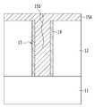
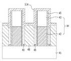
도 1a에 도시된 바와 같이, 제1층(11) 상에 제2층(12)을 형성한다. 제1층(11)은 반도체 기판을 포함할 수 있다. 제1층(11)은 도전물질 또는 절연물질을 포함할 수 있다. 제1층(11)은 실리콘을 함유할 수 있다. 제1층(11)은 실리콘기판, 실리콘저마늄기판을 포함할 수 있다. 또한, 제1층(11)은 SOI 기판을 포함할 수도 있다. 제2층(12)은 도전물질 또는 절연물질을 포함할 수 있다. 제1층(11)과 제2층(12)은 선택비를 갖는 서로 다른 절연물질을 포함할 수 있다. 제2층(12)은 실리콘산화물 또는 실리콘질화물을 포함할 수 있다.A
다음으로, 제2층(12)을 식각하여 오픈부(13)를 형성한다. 오픈부(13)는 비트라인콘택홀, 스토리지노드콘택홀 등의 홀형태의 콘택홀(Hole type contact hole)을 포함할 수 있다. 또한, 오픈부(23)는 라인 형태의 콘택홀(Line type contact hole)을 포함할 수도 있다. 다른 실시예에서, 오픈부(13)가 반도체기판을 식각하므로써 형성될 수 있고, 이때, 오픈부(13)는 콘택플러그, 매립게이트전극 또는 매립 캐패시터의 전극이 형성될 공간을 포함할 수 있다.Next, the
도 1b에 도시된 바와 같이, 오픈부(13)를 포함한 제2층(12) 상에 희생층(14A)을 형성한다. 희생층(14A)은 제2층(12)에 대해 식각선택비를 갖는 물질을 포함할 수 있다. 제2층(12)이 실리콘산화물을 포함하는 경우, 희생층(14A)은 실리콘산화물에 대해 식각선택비를 갖는 물질을 포함할 수 있다. 예를 들어, 희생층(14A)은 실리콘질화물, 보론질화물 또는 티타늄질화물을 포함할 수 있다. 제2층(12)이 실리콘질화물 또는 보론질화물을 포함하는 경우, 희생층(14A)은 실리콘산화물 또는 티타늄질화물을 포함할 수 있다.A sacrifice layer 14A is formed on the
도 1c에 도시된 바와 같이, 희생스페이서(14)를 형성한다. 희생스페이서(14)는 희생층(14A)을 식각하므로써 형성될 수 있다. 에치백 공정을 통해 희생층(14A)을 식각할 수 있다. 희생스페이서(14)는 오픈부(13)의 측벽에 형성되는 스페이서 형태가 될 수 있다.As shown in Fig. 1C,
다음으로, 오픈부(13)를 갭필하도록 전면에 폴리실리콘층(15A)을 형성한다. 폴리실리콘층(15A)을 형성하기 전에 전세정을 실시할 수 있다. 폴리실리콘층(15A)을 형성할 때, 심(Seam, 15B)이 발생될 수 있다.Next, a
도 1d에 도시된 바와 같이, 폴리실리콘층패턴(15C)을 형성한다. 폴리실리콘층패턴(15C)을 형성하기 위해 제2층(12)의 표면으로부터 폴리실리콘층(15A)을 선택적으로 제거할 수 있다. 폴리실리콘층패턴(15C)을 형성하더라도 폴리실리콘층패턴(15C) 내에 심(15B)이 여전히 존재할 수 있다.As shown in Fig. 1D, a
도 1e에 도시된 바와 같이, 희생스페이서(14)를 선택적으로 제거한다. 이에 따라, 에어갭(16)이 형성될 수 있다. 에어갭(16)은 폴리실리콘층패턴(15C)의 측벽과 제2층(12) 사이에 형성될 수 있다. 희생스페이서(14)는 습식식각을 이용하여 제거할 수 있다. 희생스페이서(14)가 실리콘질화물을 포함하는 경우, 인산 계열의 케미컬을 이용하여 제거할 수 있다. 희생스페이서(14)가 실리콘산화물을 포함하는 경우, 불산 계열의 케미컬을 이용하여 제거할 수 있다. 희생스페이서(14)가 티타늄질화물 또는 보론질화물을 포함하는 경우, 황산 계열의 케미컬을 이용하여 제거할 수 있다.As shown in FIG. 1E, the
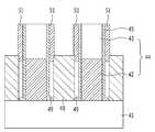
도 1f에 도시된 바와 같이, 열공정(17)을 실시한다. 이에 따라, 폴리실리콘층패턴(15C) 내에 존재하는 심(15B)이 제거된다. 부연하면, 심(15B)이 에어갭(16)쪽으로 빠져나가게 되어 모두 제거된다. 열공정(17)은 적어도 500℃ 이상의 온도에서 진행될 수 있다. 열공정(17)은 퍼니스(Furnace)를 이용한 열처리를 포함할 수 있다.As shown in Fig. 1F, a
상술한 바와 같이, 에어갭(16)이 형성된 상태에서 열공정(17)을 진행하므로서 심(15B)이 제거된다. 폴리실리콘층패턴(15C)의 측벽에 에어갭(16)이 형성되어 있음과 동시에 폴리실리콘패턴(15C)의 상부표면 또한 공기 중에 노출되어 있으므로, 심(15B)의 제거효과가 증대된다. 즉, 심(15B)은 에어갭(16)쪽으로 확산되면서 동시에 폴리실리콘층패턴(15C)의 상부 표면밖으로 확산되어 제거될 수 있다.As described above, the
본 실시예는 폴리실리콘층패턴(15C)의 주변이 에어갭(16) 및 공기와 접촉하도록 하므로써, 폴리실리콘층패턴(15C) 내에 존재하는 심(15B)이 보이드로 발전하지 않고 심(15B) 자체가 제거된다. 심(15B) 자체가 제거되는 이유는, 에어갭(16)과 폴리실리콘층패턴(15C)간의 표면장력과 제2층(12)과 폴리실리콘층패턴(15C)간의 표면장력 차이 때문이다.The present embodiment allows the periphery of the
결국, 본 실시예에 따르면, 보이드 프리 폴리실리콘층패턴(15)을 형성할 수 있다.As a result, according to this embodiment, the void-free
도 1g에 도시된 바와 같이, 열공정(17)이 진행된 후, 제3층(18)을 이용하여 에어갭(16)을 갭필할 수 있다. 제3층(18)은 절연물질을 포함할 수 있다. 제3층(18)은 실리콘산화물 또는 실리콘질화물을 포함할 수 있다.As shown in FIG. 1G, after the
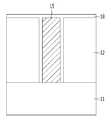
도 2a 및 도 2b는 일실시예의 비교예를 설명하기 위한 도면이다.2A and 2B are views for explaining a comparative example of the embodiment.
도 2a를 참조하면, 폴리실리콘층패턴(15C)의 측벽에 희생스페이서(14)가 잔류하는 경우에, 후속 열공정(17)을 실시하면 실리콘원자들의 이동에 의해 결정립성장이 일어나며 심(15B)의 표면적을 최소화시키는 방향으로 실리콘원자들의 이동이 일어나 보이드(15D)가 발생한다. 따라서, 희생스페이서(14)와 폴리실리콘층패턴(15C)의 계면에 보이드(15D)가 확산되어 존재하게 된다. 또한, 도 2b를 참조하면, 에어갭(16) 형성 이후에 폴리실리콘층패턴(15C) 상에 제3층(18)을 형성하는 열공정을 진행하는 경우, 폴리실리콘층패턴(15C)과 제3층(18)의 계면에 보이드(15D)가 확산되어 존재하게 된다.2A, when the
결국, 이러한 비교예들에 의해서는 보이드가 없는 폴리실리콘층패턴을 형성하기 어렵다.As a result, it is difficult to form a void-free polysilicon layer pattern by these comparative examples.
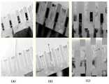
도 2c는 일실시예와 비교예에 따른 보이드 형성 정도를 도시한 도면이다.2C is a view showing the degree of void formation according to an embodiment and a comparative example.
도 2c를 참조하면, 열공정을 실시한 경우(A)에는 보이드가 관찰되지 않으나, 희생스페이서가 형성된 이후 열공정을 실시한 경우들(B, C)은 보이드(도면부호 'v' 참조)가 다발하고 있음을 알 수 있다. 도면부호 (B)는 티타늄질화물을 희생스페이서로 사용한 경우이고, 도면부호 (C)는 실리콘질화물을 희생스페이서로 사용한 경우이다.Referring to FIG. 2C, voids are not observed in the case of the thermal process (A), but cases where the thermal process is performed after the sacrificial spacer is formed are voids (see the reference symbol 'v' . Reference numeral (B) denotes a case where titanium nitride is used as a sacrificial spacer, and reference character (C) denotes a case where silicon nitride is used as a sacrificial spacer.
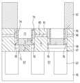
도 3a 내지 도 3h는 일실시예에 따른 보이드 프리 폴리실리콘층 형성 방법을 적용하여 반도체장치를 형성하는 방법의 일예를 나타낸 도면이다.3A to 3H are views showing an example of a method of forming a semiconductor device by applying a method of forming a void-free polysilicon layer according to an embodiment.
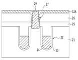
도 3a에 도시된 바와 같이, 반도체기판(21)을 식각하여 트렌치(22)를 형성한다. 트렌치(22)의 표면 상에 게이트절연층(23)을 형성한다. 반도체기판(21)은 반도체 물질을 포함할 수 있다. 반도체기판(21)은 실리콘 기판을 포함할 수 있으며, 예를 들어, 단결정 실리콘 기판을 포함할 수 있다. 도시하지 않았으나, 반도체기판(21)에 소자분리영역이 형성될 수 있다. 소자분리영역은 STI(Shallow Trench Isolation) 공정을 통해 형성할 수 있다.As shown in FIG. 3A, the
게이트절연층(23) 상에 트렌치(22)를 리세싱하는 매립게이트전극(24)을 형성한다. 매립게이트전극(24)은 트렌치(22)를 갭필하도록 금속함유층을 형성한 후 에치백하여 형성할 수 있다. 금속함유층은 티타늄, 탄탈륨, 텅스텐 등의 금속을 주성분으로 하는 물질을 포함할 수 있다. 금속함유층은 탄탈륨질화물(TaN), 티타늄질화물(TiN), 텅스텐질화물(WN) 및 텅스텐(W)으로 이루어진 그룹 중에서 선택된 적어도 어느 하나를 포함할 수 있다. 예를 들어, 매립게이트전극(24)은 티타늄질화물, 탄탈륨질화물 또는 텅스텐을 단독으로 포함하거나, 티타늄질화물(TiN) 또는 탄탈륨질화물(TaN) 상에 텅스텐(W)을 적층하는 TiN/W 또는 TaN/W과 같은 2층 구조로 형성할 수 있다. 또한, 텅스텐질화물(WN) 상에 텅스텐(W)을 적층하는 WN/W의 2층 구조를 포함할 수 있으며, 이 외에 낮은 저항의 금속물질을 포함할 수 있다.A buried
매립게이트전극(24) 상에 실링층(Sealing layer, 25A)을 형성한다. 실링층(25A)은 매립게이트전극(24) 상에서 트렌치(22)를 갭필할 수 있다. 실링층(25A)은 후속 공정으로부터 매립게이트전극(24)을 보호하는 역할을 수행할 수 있다. 실링층(25A)은 절연물질을 포함할 수 있다. 실링층(25A)은 실리콘질화물을 포함할 수 있다.A
실링층(25A) 상에 절연층(26A)을 형성한다. 절연층(26A)은 실리콘산화물을 포함할 수 있다.An insulating
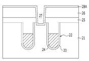
도 3b에 도시된 바와 같이, 절연층(26A)과 캡핑층(25A)을 식각하여 콘택홀(27)을 형성한다. 콘택홀(27) 형성시 반도체기판(21)의 표면을 일정 깊이 리세스시킬 수 있다. 이로써, 후속 콘택플러그의 접촉면적을 증대시킬 수 있다. 콘택홀(27)이 형성되므로써 캡핑층과 절연층은 각각 도면부호 '25'와 '26'의 형태가 된다.As shown in FIG. 3B, the insulating
도 3c에 도시된 바와 같이, 콘택홀(27)을 포함한 전면에 희생층(28A)을 형성한다. 희생층(28A)은 실리콘산화물, 실리콘질화물, 보론질화물 또는 티타늄질화물을 포함할 수 있다.A
도 3d에 도시된 바와 같이, 콘택홀(27)의 저면이 노출되도록 희생층을 식각할 수 있다. 이로써, 희생스페이서(28)가 형성된다.The sacrificial layer may be etched so that the bottom surface of the
다음으로, 콘택홀(27)을 갭필하는 콘택플러그(29A)를 형성한다. 콘택플러그(29A)를 형성하기 위해 콘택홀(27)을 갭필하도록 전면에 폴리실리콘층을 형성한 후, 절연층(26)의 표면으로부터 폴리실리콘층을 선택적으로 제거할 수 있다. 폴리실리콘층을 형성하기 전에 전세정을 실시할 수 있다. 폴리실리콘층을 형성할 때, 심(Seam, 29B)이 발생될 수 있고, 콘택플러그(29A)를 형성하더라도 콘택플러그(29A) 내에 심(29B)이 여전히 존재할 수 있다. 콘택플러그(29A)는 비트라인콘택플러그를 포함할 수 있다.Next, a
도 3e에 도시된 바와 같이, 희생스페이서(28)를 선택적으로 제거한다. 이에 따라, 에어갭(30)이 형성될 수 있다. 에어갭(30)은 콘택플러그(29A)의 측벽과 콘택홀(27)의 측벽 사이에 형성될 수 있다. 희생스페이서(28)는 습식식각을 이용하여 제거할 수 있다. 희생스페이서(28)가 실리콘질화물을 포함하는 경우, 인산 계열의 케미컬을 이용하여 제거할 수 있다. 희생스페이서(28)가 실리콘산화물을 포함하는 경우, 불산 계열의 케미컬을 이용하여 제거할 수 있다. 희생스페이서(28)가 티타늄질화물 또는 보론질화물을 포함하는 경우, 황산 계열의 케미컬을 이용하여 제거할 수 있다.As shown in FIG. 3E, the
도 3f에 도시된 바와 같이, 열공정(31)을 실시한다. 이에 따라, 콘택플러그(29A) 내에 존재하는 심(29B)이 제거된다. 부연하면, 심(29B)이 에어갭(30)쪽으로 빠져나가게 되어 모두 제거된다. 열공정(31)은 적어도 500℃ 이상의 온도에서 진행될 수 있다. 열공정(31)은 퍼니스(Furnace)를 이용한 열처리를 포함할 수 있다.As shown in FIG. 3F, a
상술한 바와 같이, 에어갭(30)이 형성된 상태에서 열공정(31)을 진행하므로서 심(29B)이 제거된다. 콘택플러그(29A)의 측벽에 에어갭(30)이 형성되어 있음과 동시에 콘택플러그(29A)의 상부표면 또한 공기 중에 노출되어 있으므로, 심(29B)의 제거효과가 증대된다. 즉, 심(29B)은 에어갭(30)쪽으로 확산되면서 동시에 콘택플러그(29A)의 상부 표면밖으로 확산되어 제거될 수 있다.As described above, the
본 실시예는 콘택플러그(29A)의 주변이 에어갭(16) 및 공기와 접촉하도록 하므로써, 콘택플러그(29A) 내에 존재하는 심(29B)이 보이드로 발전하지 않고 심(29B) 자체가 제거된다. 심(29B) 자체가 제거되는 이유는, 에어갭(30)과 콘택플러그(29A)간의 표면장력과 콘택플러그(29A)와 절연층(26) 및 캡핑층(25)간의 표면장력 차이 때문이다.The present embodiment allows the periphery of the contact plug 29A to contact the
결국, 본 실시예에 따르면, 보이드 프리 콘택플러그(29)를 형성할 수 있다.As a result, according to the present embodiment, the void-
도 3g에 도시된 바와 같이, 캡핑층(32A)을 이용하여 에어갭(30)을 갭필할 수 있다. 캡핑층(32A)은 절연물질을 포함할 수 있다. 캡핑층(32A)은 실리콘산화물 또는 실리콘질화물을 포함할 수 있다.As shown in FIG. 3G, the
도 3h에 도시된 바와 같이, 콘택플러그(29)의 표면이 노출되도록 캡핑층(32A)을 선택적으로 식각한다. 이에 따라, 캡핑층패턴(32)이 형성된다.The
콘택플러그(29) 상에 비트라인(33) 및 비트라인하드마스크층(34)을 포함하는 비트라인구조물을 형성한다. 비트라인(33)은 텅스텐층을 포함할 수 있고, Ti/TiN 등의 배리어층과 배리어층 상의 텅스텐층을 포함할 수도 있다. 비트라인하드마스크층(34)은 실리콘질화물을 포함할 수 있다.A bit line structure is formed that includes a
도 4a 내지 도 4k는 일실시예에 따른 보이드 프리 폴리실리콘층 형성 방법을 적용하여 반도체장치를 형성하는 방법의 다른예를 나타낸 도면이다.4A to 4K are views showing another example of a method of forming a semiconductor device by applying a method of forming a void-free polysilicon layer according to an embodiment.
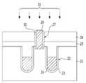
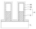
도 4a에 도시된 바와 같이, 기판(41) 상에 복수의 비트라인구조물(44)을 형성한다. 기판(41)은 실리콘을 함유할 수 있다. 기판(41)은 실리콘기판, 실리콘저마늄기판을 포함할 수 있다. 또한, 기판(41)은 SOI 기판을 포함할 수도 있다.As shown in Fig. 4A, a plurality of
기판(41) 상에 형성되는 비트라인구조물(44)은 일정 간격을 가지면서 규칙적으로 배치되는 라인 형상을 가질 수 있다. 비트라인구조물(44)을 형성하기 위해 제1도전층 상에 하드마스크패턴(43)을 형성한다. 하드마스크패턴(43)을 식각 마스크로 사용하여 제1도전층을 식각하므로써 비트라인(42)이 형성된다. 비트라인(42)과 하드마스크패턴(43)이 적층된 비트라인구조물(44)이 형성된다. 비트라인(42)은 실리콘함유층, 금속함유층을 포함할 수 있다. 예를 들어, 비트라인(42)은 폴리실리콘층 또는 텅스텐층을 포함할 수 있다. 또한, 비트라인(42)은 배리어층과 금속층을 적층하여 형성할 수 있다. 비트라인(42)은 티타늄함유층 및 텅스텐층의 적층구조물을 포함할 수 있다. 티타늄함유층은 배리어층으로서, 티타늄층과 티타늄질화물이 적층될 수 있다.The
도 4b에 도시된 바와 같이, 비트라인구조물(44)을 포함한 전면에 절연층(45A)을 형성한다. 절연층(45A)은 질화물 또는 산화물을 포함할 수 있다. 절연층(45A)은 실리콘질화물, 실리콘산화물을 포함할 수 있다. 절연층(45A)은 스페이서가 되는 물질이다.As shown in FIG. 4B, an insulating
절연층(45A) 상에 희생층(46A)을 형성한다. 희생층(46A)은 후속 공정에서 제거되어 에어갭을 형성하는 물질이다. 희생층(46A)은 절연층(45A)과 식각선택비를 갖는 물질을 포함할 수 있다. 희생층(46A)은 실리콘산화물, 실리콘질화물, 금속질화물을 포함할 수 있다. 절연층(45A)이 실리콘산화물을 포함하는 경우, 희생층(46A)은 금속질화물 또는 실리콘질화물을 포함할 수 있다. 절연층(45A)이 실리콘질화물을 포함하는 경우, 희생층(46A)은 실리콘산화물 또는 금속질화물을 포함할 수 있다. 희생층(46A)은 실리콘산화물, 실리콘질화물, 티타늄질화물(TiN)을 포함할 수 있다. 또한, 희생층(46A)은 보론질화물을 포함할 수도 있다.A
도 4c에 도시된 바와 같이, 비트라인구조물(44)의 양측벽에 이중 스페이서(Double spacer)를 형성한다. 이중 스페이서는 스페이서(45)와 희생스페이서(46)를 포함할 수 있다. 스페이서(45)는 절연층(45A)을 식각하므로써 형성될 수 있다. 스페이서(45)의 측벽에는 희생스페이서(46)가 형성될 수 있다. 희생스페이서(46)는 희생층(46A)을 식각하므로써 형성될 수 있다. 스페이서(45)와 희생스페이서(46)를 형성하기 위해, 에치백 공정이 적용될 수 있다.As shown in FIG. 4C, double spacers are formed on both side walls of the
이와 같이, 스페이서(45)과 희생스페이서(46)를 형성하므로써 비트라인구조물(44) 사이에 기판(41)을 노출시키는 스토리지노드콘택홀(47)이 형성될 수 있다. 다른 실시예에서, 스페이서(45)를 형성한 후, 층간절연층(미도시)을 형성한다. 이후, 층간절연층을 식각하여 스토리지노드콘택홀(47)을 형성한 후, 희생층 증착 및 에치백을 실시하여 스토리지노드콘택홀(47)의 측벽에 희생스페이서(46)를 형성할 수도 있다. 스토리지노드콘택홀(47)은 희생스페이서(46)의 측벽을 노출시키면서 형성될 수 있다. 스토리지노드콘택홀(47)은 라인 형상을 갖거나, 콘택홀 형상을 가질 수 있다.In this manner, the storage
도 4d에 도시된 바와 같이, 스토리지노드콘택홀(47)을 갭필하는 제2도전층(48A)을 형성한다. 제2도전층(48A)은 실리콘함유층을 포함할 수 있다. 제2도전층(48A)은 폴리실리콘층을 포함할 수 있다. 폴리실리콘층은 화학기상증착법을 이용하여 형성할 수 있다. 폴리실리콘층을 갭필할 때, 심(48B)이 발생한다.As shown in FIG. 4D, a second
도 4e에 도시된 바와 같이, 제2도전층(48A)을 선택적으로 제거한다. 이에 따라, 비트라인구조물(44) 사이에 제1콘택플러그(48C)가 리세싱된다. 제1콘택플러그(48C)를 형성하기 위해 에치백 공정이 적용될 수 있다. 제1콘택플러그(48C)는 비트라인구조물(44)의 표면보다 낮게 리세스된 표면을 갖는다. 제1콘택플러그(48C)의 리세스된 표면은 적어도 비트라인(42)의 상부 표면보다 높게 제어할 수 있다. 제1콘택플러그(48C)의 높이는 비트라인(42)과의 대향면적을 최소화시키는 높이를 가질 수 있다. 이로써, 비트라인(42)과 제1콘택플러그(48C)간의 기생캐패시턴스를 감소시킬 수 있다. 제1콘택플러그(48C)는 스토리지노드콘택플러그의 일부가 된다.As shown in FIG. 4E, the second
도 4f에 도시된 바와 같이, 희생스페이서(46)를 선택적으로 제거한다. 이에 따라, 에어갭(49)이 형성된다. 에어갭(49)은 제1콘택플러그(48C)의 측벽에 형성될 수 있다. 제1콘택플러그(48C)와 비트라인(42) 사이에 에어갭(49)이 형성된다. 비트라인(42)과 제1콘택플러그(48C) 사이에는 '에어갭(49)-스페이서(45)'의 절연구조가 형성된다.As shown in FIG. 4F, the
희생스페이서(46)를 제거하기 위해 습식식각(Wet Etch) 또는 건식식각(Dry Etch)이 적용될 수 있다. 희생스페이서(46)를 제거할 때, 스페이서(45), 제1콘택플러그(48C) 및 하드마스크패턴(43)은 선택비를 가져 손상되지 않는다. 희생스페이서(46)가 티타늄질화물인 경우, H2SO4와 H2O2가 혼합된 용액을 이용한 습식세정을 진행할 수 있다.Wet Etch or Dry Etch may be applied to remove the
위와 같이, 에어갭(49)을 형성하므로써 비트라인(42)과 제1콘택플러그(48C) 사이의 기생캐패시턴스가 감소한다.As described above, by forming the
도 4g에 도시된 바와 같이, 열공정(50)을 실시한다. 이에 따라, 제1콘택플러그(48C) 내에 존재하는 심(48B)이 제거된다. 부연하면, 심(48B)이 에어갭(49)쪽으로 빠져나가게 되어 모두 제거된다. 열공정(50)은 적어도 500℃ 이상의 온도에서 진행될 수 있다. 열공정(50)은 퍼니스(Furnace)를 이용한 열처리를 포함할 수 있다.As shown in FIG. 4g, a
상술한 바와 같이, 에어갭(49)이 형성된 상태에서 열공정(50)을 진행하므로서 심(48B)이 제거된다. 제1콘택플러그(48C)의 측벽에 에어갭(49)이 형성되어 있음과 동시에 제1콘택플러그(48C)의 상부표면 또한 공기 중에 노출되어 있으므로, 심(48B)의 제거효과가 증대된다. 즉, 심(48B)은 에어갭(49)쪽으로 확산되면서 동시에 콘택플러그(48C)의 상부 표면밖으로 확산되어 제거될 수 있다.As described above, the
본 실시예는 제1콘택플러그(48C)의 주변이 에어갭(49) 및 공기와 접촉하도록 하므로써, 제1콘택플러그(48C) 내에 존재하는 심(48B)이 보이드로 발전하지 않고 심(48B) 자체가 제거된다. 이로써 보이드가 없는(Void-free) 제1콘택플러그(48)가 형성된다.The present embodiment allows the periphery of the first contact plug 48C to be in contact with the
도 4h에 도시된 바와 같이, 제1콘택플러그(48) 상에 에어갭(49)을 캡핑하는 캡핑층(51A)을 형성한다. 캡핑층(51A)은 절연물질을 포함할 수 있다. 캡핑층(51A)은 실리콘산화물 또는 실리콘질화물을 포함할 수 있다. 캡핑층(51A)은 에어갭(49)을 갭필하지 않는 두께로 형성할 수 있다.A
도 4i에 도시된 바와 같이, 캡핑층(51A)을 선택적으로 제거한다. 이에 따라, 캡핑스페이서(51)가 형성된다. 캡핑스페이서(51)는 에어갭(49)을 캡핑함과 동시에 제1콘택플러그(48) 상에서 오픈부의 상부 측벽을 캡핑한다.As shown in Fig. 4I, the
도시하지 않았으나, 캡핑스페이서(51) 형성 이후에 후속공정으로서 이온주입을 실시할 수 있다. 이온주입은 콘택저항 개선을 위해 실시한다.Although not shown, after the capping
도 4j에 도시된 바와 같이, 제1콘택플러그(48) 상에 금속실리사이드(52)를 형성한다. 금속실리사이드(52)를 형성하기 위해 금속층(미도시)을 전면에 형성한 후, 어닐을 실시할 수 있다. 금속층은 실리사이드화가능물질을 포함할 수 있다. 금속층은 코발트를 포함할 수 있다. 어닐에 의해 금속층과 제1콘택플러그(48)의 실리콘이 반응하여 금속실리사이드(52)가 형성될 수 있다. 금속실리사이드(52)는 코발트실리사이드를 포함할 수 있다. 본 실시예에서, 금속실리사이드(52)는 'CoSi2상'의 코발트실리사이드를 포함할 수 있다.A
금속실리사이드(52)로서 CoSi2상의 코발트실리사이드를 형성하므로써 콘택저항을 개선시킴과 동시에 미세 선폭을 갖는 스토리지노드콘택홀(47)의 작은 면적에서도 충분히 저저항의 코발트실리사이드를 형성할 수 있다. 금속실리사이드(52)는 오믹콘택층의 역할을 수행할 수 있다.By forming cobalt silicide on the CoSi2 phase as the
도 4k에 도시된 바와 같이, 미반응 금속층을 스트립한다. 미반응 금속층을 제거하지 않으면, 후속 공정에서 미반응 금속층의 금속원자가 하부로 확산하거나, 금속실리사이드(52)의 이상 반응을 일으킬 수 있다. 따라서, 미반응 금속층을 제거한다. 미반응 금속층은 습식케미컬을 이용한 세정 공정을 통해 제거할 수 있다. 예를 들어, 미반응 금속층이 코발트인 경우, H2SO4(SPM)과 NH4OH(SC-1) 계열의 케미컬을 이용할 수 있다. 부연하면, 탈이온수(DI Water)를 이용하여 미반응 금속층을 산화시키고, H2SO4(SPM)과를 이용하여 1차 제거를 하고, 잔류하는 금속성폴리머 계열의 잔류물(Residue)을 NH4OH 계열의 케미컬을 이용하여 2차 제거한다.As shown in Figure 4K, the unreacted metal layer is stripped. Unless the unreacted metal layer is removed, the metal atoms of the unreacted metal layer may diffuse downward in the subsequent process, or an abnormal reaction of the
이와 같이, 습식케미컬을 이용하므로써 미반응 금속층은 물론 금속성 폴리머를 깨끗하게 제거할 수 있다.Thus, by using the wet chemical, the unreacted metal layer as well as the metallic polymer can be cleanly removed.
다음으로, 금속실리사이드(52) 상에 제2콘택플러그(53)를 형성할 수 있다. 제2콘택플러그(53)를 형성하기 위해 금속실리사이드(52)의 상부를 갭필하는 제3도전층을 형성한 후, 평탄화 공정을 진행할 수 있다. 제2콘택플러그(53)는 금속함유층을 포함할 수 있다. 제2콘택플러그(53)는 텅스텐층을 포함할 수 있다. 도시하지 않았으나, 제2콘택플러그(53)는 배리어층을 더 포함할 수 있다. 따라서, 제2콘택플러그(53)는 배리어층과 금속함유층을 적층하여 형성할 수 있다. 배리어층은 티타늄을 함유하는 물질을 포함할 수 있다. 배리어층은 티타늄을 단독으로 형성하거나 또는 티타늄과 티타늄질화물을 적층하여 형성할 수 있다.Next, a
위와 같이, 제2콘택플러그(53)를 형성하면, 제1콘택플러그(48), 금속실리사이드(52) 및 제2콘택플러그(53)를 포함하는 스토리지노드콘택플러그(54)이 형성된다. 비트라인구조물(44)과 스토리지노드콘택플러그(54) 사이에는 에어갭(49)이 형성된다. 제1콘택플러그(48)는 스토리지노드콘택플러그(54)의 하부 플러그(Bottom plug)가 되고, 제2콘택플러그(53)는 스토리지노드콘택플러그(54)의 상부 플러그(Top plug)가 될 수 있다. 제1콘택플러그(48)가 실리콘함유층을 포함하고, 제2콘택플러그(53)가 금속함유층을 포함하므로, 실리콘함유층과 금속함유층을 포함하는 콘택플러그, 즉, 세미메탈 콘택플러그 구조가 형성될 수 있다. 다른 실시예에서, 스토리지노드콘택플러그(54)는 폴리실리콘층을 이용한 이중 플러그 구조를 가질 수도 있다. 이때는 금속실리사이드가 필요없을 수 있다.As described above, when the
에어갭(49)은 비트라인(42)과 제1콘택플러그(48) 사이에 형성될 수 있다.An
도 5a는 DRAM의 메모리셀을 도시한 배치도이고, 도 5b는 도 5a의 A-A'선에 따른 단면도이다. 도 5c는 도 5a의 B-B'선에 따른 단면도이다.5A is a layout diagram showing a memory cell of a DRAM, and FIG. 5B is a cross-sectional view taken along line A-A 'of FIG. 5A. 5C is a cross-sectional view taken along the line B-B 'in FIG. 5A.
도 5a, 도 5b 및 도 5c를 참조하면, 기판(61)에 소자분리영역(62)에 의해 활성영역(63)이 정의된다. 활성영역(63)과 소자분리영역(62)을 가로지르는 트렌치(64)에 매립게이트전극(66)이 형성된다. 매립게이트전극(66)과 교차하는 방향으로 연장된 비트라인(72)이 기판(61) 상부에 형성되며, 비트라인(72)은 비트라인콘택플러그(70)를 통해 활성영역(63)과 연결된다. 활성영역(63)에 연결되는 스토리지노드콘택플러그가 형성된다. 스토리지노드콘택플러그는 제1콘택플러그(77), 금속실리사이드(80) 및 제2콘택플러그(81)가 적층될 수 있다. 스토리지노드콘택플러그의 제2플러그(81) 상에 캐패시터의 스토리지노드(82)가 형성된다.5A, 5B and 5C, the
스토리지노드콘택플러그는 본 실시예들에 따른 스토리지노드콘택플러그에 대응할 수 있고, 비트라인(72)은 비트라인구조물의 비트라인에 대응할 수 있다. 따라서, 스토리지노드콘택플러그와 비트라인(72) 사이에 에어갭(78)이 형성될 수 있다. 스토리지노드콘택플러그는 제1콘택플러그(77)와 제2콘택플러그(81)를 포함할 수 있다. 캡핑스페이서(79)는 제1콘택플러그(77) 및 에어갭(78)을 캡핑할 수 있다. 캡핑스페이서(79)는 본 실시예들에 따른 캡핑스페이서에 대응될 수 있다.The storage node contact plug may correspond to the storage node contact plug according to the embodiments, and the
도 5a, 도 5b 및 도 5c를 참조하여 메모리셀의 제조 방법을 살펴보면 다음과 같다.A method of manufacturing a memory cell will be described with reference to FIGS. 5A, 5B, and 5C.
기판(61)은 반도체 물질을 포함할 수 있다. 기판(61)은 반도체기판을 포함할 수 있다. 기판(61)은 실리콘 기판을 포함할 수 있으며, 예를 들어, 단결정 실리콘 기판을 포함할 수 있다. 소자분리영역(62)은 STI(Shallow Trench Isolation) 공정을 통해 형성할 수 있다. 소자분리영역(62)에 의해 활성영역(63)이 정의될 수 있다. 소자분리영역(62)은 측벽산화물(Wall oxide), 라이너(liner) 및 갭필물질(Gapfill material)을 순차적으로 형성할 수 있다. 라이너는 실리콘질화물(Silicon nitride), 실리콘산화물(Silicon oxide)을 포함할 수 있다. 실리콘질화물은 Si3N4를 포함할 수 있고, 실리콘산화물은 SiO2를 포함할 수 있다. 갭필물질은 스핀온절연물(SOD) 등의 실리콘산화물을 포함할 수 있다. 또한, 갭필물질은 실리콘질화물을 포함할 수 있으며, 이때, 실리콘질화물은 라이너로 사용되는 실리콘질화물을 이용하여 갭필할 수 있다.The
트렌치(64)는 활성영역(63)과 소자분리영역(62)에서 동시에 형성될 수 있다. 활성영역(63)과 소자분리영역(62)의 식각률 차이에 의해 소자분리영역(62)에서 더 깊게 형성될 수 있다.The
매립게이트전극(66)을 형성하기 전에 트렌치(64)의 표면에 게이트절연층(65)을 형성할 수 있다. 매립게이트전극(66)은 트렌치(64)를 갭필하도록 금속함유층을 형성한 후 에치백하여 형성할 수 있다. 금속함유층은 티타늄, 탄탈륨, 텅스텐 등의 금속을 주성분으로 하는 물질을 포함할 수 있다. 금속함유층은 탄탈륨질화물(TaN), 티타늄질화물(TiN), 텅스텐질화물(WN) 및 텅스텐(W)으로 이루어진 그룹 중에서 선택된 적어도 어느 하나를 포함할 수 있다. 예를 들어, 매립게이트전극(57)은 티타늄질화물, 탄탈륨질화물 또는 텅스텐을 단독으로 포함하거나, 티타늄질화물(TiN) 또는 탄탈륨질화물(TaN) 상에 텅스텐(W)을 적층하는 TiN/W 또는 TaN/W과 같은 2층 구조로 형성할 수 있다. 또한, 텅스텐질화물(WN) 상에 텅스텐(W)을 적층하는 WN/W의 2층 구조를 포함할 수 있으며, 이 외에 낮은 저항의 금속물질을 포함할 수 있다.The
매립게이트전극(66) 상에 실링층(Sealing layer, 67)을 형성한다. 실링층(67)은 매립게이트전극(66) 상에서 트렌치(64)를 갭필할 수 있다. 실링층(67)은 후속 공정으로부터 매립게이트전극(66)을 보호하는 역할을 수행할 수 있다. 실링층(67)은 절연물질을 포함할 수 있다. 실링층(67)은 실리콘질화물을 포함할 수 있다.A
제1층간절연층(68)을 형성한 후 제1층간절연층(68)과 실링층(67)을 식각하여 비트라인콘택홀(69)을 형성한다. 비트라인콘택홀(69)에 폴리실리콘층을 형성하여 비트라인콘택플러그(70)를 형성한다. 비트라인콘택플러그(70) 상에 비트라인(72)과 비트라인하드마스크층(73)을 포함하는 비트라인구조물을 형성한다. 비트라인콘택플러그(70)는 보이드 프리 폴리실리콘층을 포함할 수 있으며, 보이드 프리 폴리실리콘층 형성 방법은 상술한 실시예들을 참고하기로 한다. 비트라인콘택플러그(70)의 측벽에 캡핑층(71)이 형성될 수 있다. 비트라인(72)은 텅스텐층을 포함할 수 있고, Ti/TiN 등의 배리어층과 배리어층 상의 텅스텐층을 포함할 수도 있다. 비트라인하드마스크층(73)은 실리콘질화물을 포함할 수 있다.After forming the first
비트라인구조물의 양측벽에 스페이서(74)를 형성한다. 이후, 제2층간절연층(75)을 형성한 후, 제2층간절연층(75), 제1층간절연층(68) 및 실링층(67)을 식각하여 스토리지노드콘택홀(76)을 형성한다. 스토리지노드콘택홀(76)에 폴리실리콘층을 이용하여 제1콘택플러그(77)를 리세싱시킨 후, 희생스페이서를 제거하여 에어갭(78)을 형성한다.
다음으로, 열공정을 실시하여 제1콘택플러그(77)의 심을 제거하므로써 보이드 프리 제1콘택플러그(77)을 형성한다.Next, a thermal process is performed to remove the shim of the
캡핑스페이서(79)를 이용하여 에어갭(78)을 캡핑한다.The capping
제1콘택플러그(77) 상에 금속실리사이드(80) 및 제2콘택플러그(81)를 형성한다. 제2콘택플러그(81)는 금속함유층을 포함할 수 있다. 제2콘택플러그(81)은 텅스텐층을 포함할 수 있다. 도시하지 않았으나, 제2콘택플러그(81)은 배리어층을 더 포함할 수 있다. 따라서, 제2콘택플러그(81)은 배리어층과 금속함유층을 적층하여 형성할 수 있다. 배리어층은 티타늄을 함유하는 물질을 포함할 수 있다. 배리어층은 티타늄을 단독으로 형성하거나 또는 티타늄과 티타늄질화물을 적층하여 형성할 수 있다.A
제2콘택플러그(81) 상에 캐패시터의 스토리지노드(82)를 형성한다. 스토리지노드(82)는 실린더형태일 수 있고, 다른 실시예에서 필라 형태를 가질 수도 있다. 도시하지 않았지만, 스토리지노드(82) 상에 유전층 및 플레이트노드를 더 형성할 수 있다.And the
상술한 실시예들에 따른 콘택구조물은 DRAM(Dynamic Random Access Memory)에 적용될 수 있으며, 이에 한정되지 않고 SRAM(Static Random Access Memory), 플래시메모리(Flash Memory), FeRAM(Ferroelectric Random Access Memory), MRAM(Magnetic Random Access Memory), PRAM(Phase Change Random Access Memory) 등의 메모리에 적용될 수 있다.The contact structure according to the above embodiments may be applied to a dynamic random access memory (DRAM), and the contact structure is not limited thereto, and may be a static random access memory (SRAM), a flash memory, a ferroelectric random access memory (FeRAM) (Magnetic Random Access Memory), and a PRAM (Phase Change Random Access Memory).
도 6은 메모리 카드를 보여주는 개략도이다. 도 6을 참조하면, 메모리 카드(300)는 제어기(310) 및 메모리(320)를 포함할 수 있다. 제어기(310) 및 메모리(320)는 전기적인 신호를 교환할 수 있다. 예를 들면, 제어기(310)의 명령에 따라서 메모리(320) 및 제어기(310)는 데이터를 주고받을 수 있다. 이에 따라, 메모리 카드(300)는 메모리(320)에 데이터를 저장하거나 또는 메모리(320)로부터 데이터를 외부로 출력할 수 있다. 메모리(320)의 특정 부분에는 앞서 설명한 바와 같은 콘택구조물들을 포함할 수 있다. 이러한 메모리 카드(300)는 다양한 휴대용 기기의 데이터 저장 매체로 이용될 수 있다. 예를 들면, 메모리 카드(300)는 메모리 스틱 카드(memory stick card), 스마트 미디어 카드(smart media card, SM), 씨큐어 디지털 카드(secure digital, SD), 미니 씨큐어 디지털 카드(mini secure digital card, mini SD), 또는 멀티 미디어 카드(multi media card, MMC) 등을 포함할 수 있다.6 is a schematic view showing a memory card; Referring to FIG. 6, the
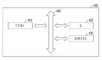
도 7은 전자 시스템을 보여주는 블록도이다. 도 7을 참조하면, 전자 시스템(400)은 프로세서(410), 입/출력 장치(430) 및 칩(420)을 포함할 수 있고, 이들은 버스(440)를 이용하여 서로 데이터 통신을 할 수 있다. 프로세서(410)는 프로그램을 실행하고, 전자 시스템(400)을 제어하는 역할을 할 수 있다. 입/출력 장치(430)는 전자 시스템(400)의 데이터를 입력 또는 출력하는데 이용될 수 있다. 전자 시스템(400)은 입/출력 장치(430)를 이용하여 외부 장치, 예를 들면 개인용 컴퓨터 또는 네트워크에 연결되어, 외부 장치와 서로 데이터를 교환할 수 있다. 칩(420)은 프로세서(410)의 동작을 위한 코드 및 데이터를 저장할 수 있고, 프로세스(410)에서 주어지는 동작을 일부 처리할 수 있다. 예를 들면, 칩(420)은 앞서 설명한 콘택구조물들을 포함할 수 있다. 전자 시스템(400)은 칩(420)을 필요로 하는 다양한 전자 제어 장치를 구성할 수 있으며, 예를 들면 모바일 폰(mobile phone), MP3 플레이어, 네비게이션(navigation), 고상 디스크 (solid state disk: SSD), 가전 제품(household appliances) 등에 이용될 수 있다.7 is a block diagram showing an electronic system. 7, the
전술한 본 발명은 전술한 실시예 및 첨부된 도면에 의해 한정되는 것이 아니고, 본 발명의 기술적 사상을 벗어나지 않는 범위 내에서 여러 가지 치환, 변형 및 변경이 가능하다는 것이 본 발명이 속하는 기술분야에서 통상의 지식을 가진 자에게 있어 명백할 것이다.It will be apparent to those skilled in the art that various modifications and variations can be made in the present invention without departing from the spirit or scope of the invention as defined by the appended claims. Will be clear to those who have knowledge of.
21 : 반도체 기판 22 : 트렌치
23 : 게이트절연층 24 : 매립게이트전극
25 : 실링층 26 : 절연층
29 : 비트라인콘택플러그 30 : 에어갭
32 : 캡핑층 33 : 비트라인
34 : 비트라인하드마스크층21: semiconductor substrate 22: trench
23: gate insulating layer 24: buried gate electrode
25: sealing layer 26: insulating layer
29: bit line contact plug 30: air gap
32: capping layer 33: bit line
34: bit line hardmask layer
Claims (23)
Translated fromKorean상기 제2층을 식각하여 오픈부를 형성하는 단계;
상기 오픈부의 측벽에 희생스페이서를 형성하는 단계;
상기 오픈부에 리세스된 폴리실리콘층패턴을 형성하는 단계;
상기 희생스페이서를 제거하여 상기 오픈부의 측벽과 상기 폴리실리콘층패턴의 측벽 사이에 에어갭을 형성하는 단계; 및
열공정을 실시하여 상기 폴리실리콘층패턴 내에 존재하는 심을 제거하는 단계
를 포함하는 반도체장치 제조 방법.
Forming a second layer on the first layer;
Etching the second layer to form an open portion;
Forming a sacrificial spacer on a sidewall of the open portion;
Forming a recessed polysilicon layer pattern in the open portion;
Removing the sacrificial spacers to form an air gap between a sidewall of the open portion and a sidewall of the polysilicon layer pattern; And
Performing a thermal process to remove shims present in the polysilicon layer pattern
≪ / RTI >
상기 열공정 단계 이후에,
상기 에어갭을 갭필하는 캡핑층을 형성하는 단계를 더 포함하는 반도체장치 제조 방법.
The method according to claim 1,
After the thermal processing step,
Further comprising forming a capping layer to cover the air gap.
상기 열공정은, 적어도 500℃ 이상의 온도에서 진행하는 반도체장치 제조 방법.
The method according to claim 1,
Wherein the thermal processing is performed at a temperature of at least 500 캜.
상기 열공정은, 퍼니스 어닐 또는 급속어닐을 포함하는 반도체장치 제조 방법.
The method according to claim 1,
Wherein the thermal processing includes a furnace anneal or a rapid anneal.
상기 오픈부에 리세스된 폴리실리콘층패턴을 형성하는 단계는,
상기 오픈부를 갭필하도록 상기 제2층 상에 폴리실리콘층을 형성하는 단계;
상기 폴리실리콘층을 에치백하는 단계
를 포함하는 반도체장치 제조 방법.
The method according to claim 1,
Wherein forming the recessed polysilicon layer pattern in the open portion comprises:
Forming a polysilicon layer on the second layer to fill the opening;
Etching back the polysilicon layer
≪ / RTI >
상기 희생스페이서는 티타늄질화물, 실리콘산화물 또는 보론질화물을 포함하는 반도체장치 제조 방법.
The method according to claim 1,
Wherein the sacrificial spacer comprises titanium nitride, silicon oxide or boron nitride.
상기 매립게이트전극의 상부에 절연층을 형성하는 단계;
상기 절연층을 식각하여 상기 반도체기판을 노출시키는 콘택홀을 형성하는 단계;
상기 콘택홀의 측벽에 희생스페이서를 형성하는 단계;
상기 콘택홀에 리세스된 폴리실리콘층패턴을 형성하는 단계;
상기 희생스페이서를 제거하여 상기 콘택홀의 측벽과 상기 폴리실리콘층패턴의 측벽 사이에 에어갭을 형성하는 단계; 및
열공정을 실시하여 상기 폴리실리콘층패턴 내에 존재하는 심을 제거하는 단계
를 포함하는 반도체장치 제조 방법.
Forming a buried gate electrode on a semiconductor substrate;
Forming an insulating layer on the buried gate electrode;
Etching the insulating layer to form a contact hole exposing the semiconductor substrate;
Forming a sacrificial spacer on a sidewall of the contact hole;
Forming a recessed polysilicon layer pattern in the contact hole;
Removing the sacrificial spacers to form an air gap between a sidewall of the contact hole and a sidewall of the polysilicon layer pattern; And
Performing a thermal process to remove shims present in the polysilicon layer pattern
≪ / RTI >
상기 열공정 단계 이후에,
상기 에어갭을 갭필하는 캡핑층을 형성하는 단계를 더 포함하는 반도체장치 제조 방법.
8. The method of claim 7,
After the thermal processing step,
Further comprising forming a capping layer to cover the air gap.
상기 열공정은, 적어도 500℃ 이상의 온도에서 진행하는 반도체장치 제조 방법.
8. The method of claim 7,
Wherein the thermal processing is performed at a temperature of at least 500 캜.
상기 열공정은, 퍼니스 어닐 또는 급속어닐을 포함하는 반도체장치 제조 방법.
8. The method of claim 7,
Wherein the thermal processing includes a furnace anneal or a rapid anneal.
상기 희생스페이서는 티타늄질화물, 실리콘산화물 또는 보론질화물을 포함하는 반도체장치 제조 방법.
8. The method of claim 7,
Wherein the sacrificial spacer comprises titanium nitride, silicon oxide or boron nitride.
상기 폴리실리콘층패턴은 비트라인콘택플러그 또는 스토리지노드콘택플러그를 포함하는 반도체장치 제조 방법.
8. The method of claim 7,
Wherein the polysilicon layer pattern comprises a bit line contact plug or a storage node contact plug.
상기 복수의 비트라인구조물 사이에 스토리지노드콘택홀을 형성하는 단계;
상기 스토리지노드콘택홀의 측벽에 희생스페이서를 형성하는 단계;
상기 스토리지노드콘택홀 내에 폴리실리콘층을 이용하여 리세스된 제1콘택플러그를 형성하는 단계;
상기 희생스페이서를 제거하여 상기 스토리지노드콘택홀의 측벽과 상기 제1콘택플러그의 측벽 사이에 에어갭을 형성하는 단계;
열공정을 실시하여 상기 제1콘택플러그 내에 존재하는 심을 제거하는 단계;
상기 에어갭을 캡핑하는 캡핑스페이서를 형성하는 단계; 및
상기 제1콘택플러그 상에 제2콘택플러그를 형성하는 단계
를 포함하는 반도체장치 제조 방법.
Forming a plurality of bit line structures on a semiconductor substrate;
Forming a storage node contact hole between the plurality of bit line structures;
Forming a sacrificial spacer on a sidewall of the storage node contact hole;
Forming a recessed first contact plug using a polysilicon layer in the storage node contact hole;
Removing the sacrificial spacers to form an air gap between a sidewall of the storage node contact hole and a sidewall of the first contact plug;
Performing a thermal process to remove shims present in the first contact plug;
Forming a capping spacer to cap the air gap; And
Forming a second contact plug on the first contact plug
≪ / RTI >
상기 희생스페이서를 형성하는 단계는,
상기 스토리지노드콘택홀을 포함한 전면에 희생층을 형성하는 단계; 및
상기 희생층을 식각하여 상기 희생스페이서를 형성하는 단계
를 포함하는 반도체장치 제조 방법.
14. The method of claim 13,
Wherein forming the sacrificial spacer comprises:
Forming a sacrificial layer on the entire surface including the storage node contact hole; And
Etching the sacrificial layer to form the sacrificial spacer
≪ / RTI >
상기 리세스된 제1콘택플러그를 형성하는 단계는,
상기 스토리지노드콘택홀을 갭필하는 폴리실리콘층을 형성하는 단계; 및
상기 폴리실리콘층을 에치백하는 단계
를 포함하는 반도체장치 제조 방법.
14. The method of claim 13,
Wherein forming the recessed first contact plug comprises:
Forming a polysilicon layer to glue the storage node contact holes; And
Etching back the polysilicon layer
≪ / RTI >
상기 열공정은, 적어도 500℃ 이상의 온도에서 진행하는 반도체장치 제조 방법.
14. The method of claim 13,
Wherein the thermal processing is performed at a temperature of at least 500 캜.
상기 열공정은, 퍼니스 어닐 또는 급속어닐을 포함하는 반도체장치 제조 방법.
14. The method of claim 13,
Wherein the thermal processing includes a furnace anneal or a rapid anneal.
상기 희생스페이서는 티타늄질화물, 실리콘산화물 또는 보론질화물을 포함하는 반도체장치 제조 방법.
14. The method of claim 13,
Wherein the sacrificial spacer comprises titanium nitride, silicon oxide or boron nitride.
상기 제2콘택플러그는 금속함유물질을 포함하는 반도체장치 제조 방법.
14. The method of claim 13,
Wherein the second contact plug comprises a metal-containing material.
상기 캡핑스페이서를 형성하는 단계는,
상기 제1콘택플러그 및 에어갭을 덮는 절연층을 형성하는 단계;
상기 제1콘택플러그의 표면을 노출시키고 상기 에어갭을 캡핑하도록 상기 절연층을 에치백하는 단계
를 포함하는 반도체장치 제조 방법.
14. The method of claim 13,
Wherein forming the capping spacer comprises:
Forming an insulating layer covering the first contact plug and the air gap;
Etching the insulating layer to expose a surface of the first contact plug and to cap the air gap
≪ / RTI >
상기 콘택홀에 형성된 콘택플러그;
상기 콘택플러그의 측벽과 상기 콘택홀의 측벽 사이에 형성된 에어갭; 및
상기 에어갭을 갭필하는 제2절연층을 포함하고,
상기 콘택플러그는 상기 에어갭이 오픈된 상태에서 열처리된 폴리실리콘층을 포함하는 반도체장치.
A first insulating layer having a contact hole exposing a part of the surface of the substrate;
A contact plug formed in the contact hole;
An air gap formed between a side wall of the contact plug and a side wall of the contact hole; And
And a second insulating layer for gripping the air gap,
Wherein the contact plug comprises a polysilicon layer heat-treated with the air gap open.
상기 콘택플러그는 스토리지노드콘택플러그를 포함하는 반도체장치.
22. The method of claim 21,
Wherein the contact plug comprises a storage node contact plug.
상기 콘택플러그는, 제1플러그, 오믹콘택층 및 제2플러그의 순서로 적층되고, 상기 제1플러그와 콘택홀의 측벽 사이에 상기 에어갭이 형성된 반도체장치.22. The method of claim 21,
The contact plug is stacked in the order of the first plug, the ohmic contact layer, and the second plug, and the air gap is formed between the first plug and the side wall of the contact hole.
Priority Applications (3)
| Application Number | Priority Date | Filing Date | Title |
|---|---|---|---|
| KR1020120153822AKR101950349B1 (en) | 2012-12-26 | 2012-12-26 | Method for gapfilling void―free polysilicon and mehto for fabricating semiconductor device using the same |
| US13/845,414US9287163B2 (en) | 2012-12-26 | 2013-03-18 | Method for forming void-free polysilicon and method for fabricating semiconductor device using the same |
| US15/013,389US9460964B2 (en) | 2012-12-26 | 2016-02-02 | Method for forming void-free polysilicon and method for fabricating semiconductor device using the same |
Applications Claiming Priority (1)
| Application Number | Priority Date | Filing Date | Title |
|---|---|---|---|
| KR1020120153822AKR101950349B1 (en) | 2012-12-26 | 2012-12-26 | Method for gapfilling void―free polysilicon and mehto for fabricating semiconductor device using the same |
Publications (2)
| Publication Number | Publication Date |
|---|---|
| KR20140083746A KR20140083746A (en) | 2014-07-04 |
| KR101950349B1true KR101950349B1 (en) | 2019-02-20 |
Family
ID=50975098
Family Applications (1)
| Application Number | Title | Priority Date | Filing Date |
|---|---|---|---|
| KR1020120153822AActiveKR101950349B1 (en) | 2012-12-26 | 2012-12-26 | Method for gapfilling void―free polysilicon and mehto for fabricating semiconductor device using the same |
Country Status (2)
| Country | Link |
|---|---|
| US (2) | US9287163B2 (en) |
| KR (1) | KR101950349B1 (en) |
Families Citing this family (279)
| Publication number | Priority date | Publication date | Assignee | Title |
|---|---|---|---|---|
| US20130023129A1 (en) | 2011-07-20 | 2013-01-24 | Asm America, Inc. | Pressure transmitter for a semiconductor processing environment |
| US10714315B2 (en) | 2012-10-12 | 2020-07-14 | Asm Ip Holdings B.V. | Semiconductor reaction chamber showerhead |
| US20160376700A1 (en) | 2013-02-01 | 2016-12-29 | Asm Ip Holding B.V. | System for treatment of deposition reactor |
| US10497776B2 (en)* | 2013-06-19 | 2019-12-03 | Taiwan Semiconductor Manufacturing Co., Ltd. | Narrow gap device with parallel releasing structure |
| JP2015122471A (en)* | 2013-11-20 | 2015-07-02 | マイクロン テクノロジー, インク. | Semiconductor device and manufacturing method of the same |
| US10941490B2 (en) | 2014-10-07 | 2021-03-09 | Asm Ip Holding B.V. | Multiple temperature range susceptor, assembly, reactor and system including the susceptor, and methods of using the same |
| KR102334110B1 (en)* | 2014-10-24 | 2021-12-02 | 삼성전자주식회사 | Method of forming a semiconductor device |
| KR102321390B1 (en)* | 2014-12-18 | 2021-11-04 | 에스케이하이닉스 주식회사 | Semiconductor device with air gap and method for fabricating the same |
| US10276355B2 (en) | 2015-03-12 | 2019-04-30 | Asm Ip Holding B.V. | Multi-zone reactor, system including the reactor, and method of using the same |
| KR102352232B1 (en) | 2015-06-15 | 2022-01-17 | 삼성전자주식회사 | Method of fabricating semiconductor device having contact structures |
| US10458018B2 (en) | 2015-06-26 | 2019-10-29 | Asm Ip Holding B.V. | Structures including metal carbide material, devices including the structures, and methods of forming same |
| TWI567752B (en)* | 2015-08-07 | 2017-01-21 | 華邦電子股份有限公司 | Memory device and method of fabricating the same |
| US10211308B2 (en) | 2015-10-21 | 2019-02-19 | Asm Ip Holding B.V. | NbMC layers |
| US9716154B2 (en) | 2015-12-17 | 2017-07-25 | Taiwan Semiconductor Manufacturing Co., Ltd. | Semiconductor structure having a gas-filled gap |
| US11139308B2 (en) | 2015-12-29 | 2021-10-05 | Asm Ip Holding B.V. | Atomic layer deposition of III-V compounds to form V-NAND devices |
| US9583400B1 (en)* | 2016-01-15 | 2017-02-28 | International Business Machines Corporation | Gate stack with tunable work function |
| US10529554B2 (en) | 2016-02-19 | 2020-01-07 | Asm Ip Holding B.V. | Method for forming silicon nitride film selectively on sidewalls or flat surfaces of trenches |
| US10343920B2 (en) | 2016-03-18 | 2019-07-09 | Asm Ip Holding B.V. | Aligned carbon nanotubes |
| US11453943B2 (en) | 2016-05-25 | 2022-09-27 | Asm Ip Holding B.V. | Method for forming carbon-containing silicon/metal oxide or nitride film by ALD using silicon precursor and hydrocarbon precursor |
| US9812319B1 (en)* | 2016-07-06 | 2017-11-07 | Asm Ip Holding B.V. | Method for forming film filled in trench without seam or void |
| US9859151B1 (en) | 2016-07-08 | 2018-01-02 | Asm Ip Holding B.V. | Selective film deposition method to form air gaps |
| US10612137B2 (en) | 2016-07-08 | 2020-04-07 | Asm Ip Holdings B.V. | Organic reactants for atomic layer deposition |
| US9887082B1 (en) | 2016-07-28 | 2018-02-06 | Asm Ip Holding B.V. | Method and apparatus for filling a gap |
| US9812320B1 (en) | 2016-07-28 | 2017-11-07 | Asm Ip Holding B.V. | Method and apparatus for filling a gap |
| US9941352B1 (en) | 2016-10-05 | 2018-04-10 | International Business Machines Corporation | Transistor with improved air spacer |
| US11532757B2 (en) | 2016-10-27 | 2022-12-20 | Asm Ip Holding B.V. | Deposition of charge trapping layers |
| US10714350B2 (en) | 2016-11-01 | 2020-07-14 | ASM IP Holdings, B.V. | Methods for forming a transition metal niobium nitride film on a substrate by atomic layer deposition and related semiconductor device structures |
| KR102546317B1 (en) | 2016-11-15 | 2023-06-21 | 에이에스엠 아이피 홀딩 비.브이. | Gas supply unit and substrate processing apparatus including the same |
| KR102762543B1 (en) | 2016-12-14 | 2025-02-05 | 에이에스엠 아이피 홀딩 비.브이. | Substrate processing apparatus |
| US11581186B2 (en) | 2016-12-15 | 2023-02-14 | Asm Ip Holding B.V. | Sequential infiltration synthesis apparatus |
| US11447861B2 (en) | 2016-12-15 | 2022-09-20 | Asm Ip Holding B.V. | Sequential infiltration synthesis apparatus and a method of forming a patterned structure |
| US10269558B2 (en) | 2016-12-22 | 2019-04-23 | Asm Ip Holding B.V. | Method of forming a structure on a substrate |
| US11390950B2 (en) | 2017-01-10 | 2022-07-19 | Asm Ip Holding B.V. | Reactor system and method to reduce residue buildup during a film deposition process |
| US10468261B2 (en) | 2017-02-15 | 2019-11-05 | Asm Ip Holding B.V. | Methods for forming a metallic film on a substrate by cyclical deposition and related semiconductor device structures |
| WO2018187546A1 (en) | 2017-04-07 | 2018-10-11 | Applied Materials, Inc. | Gapfill using reactive anneal |
| CN108766969B (en)* | 2017-04-13 | 2023-10-13 | 三星电子株式会社 | Method of manufacturing semiconductor memory device |
| US10770286B2 (en) | 2017-05-08 | 2020-09-08 | Asm Ip Holdings B.V. | Methods for selectively forming a silicon nitride film on a substrate and related semiconductor device structures |
| US12040200B2 (en) | 2017-06-20 | 2024-07-16 | Asm Ip Holding B.V. | Semiconductor processing apparatus and methods for calibrating a semiconductor processing apparatus |
| US11306395B2 (en) | 2017-06-28 | 2022-04-19 | Asm Ip Holding B.V. | Methods for depositing a transition metal nitride film on a substrate by atomic layer deposition and related deposition apparatus |
| KR20190009245A (en) | 2017-07-18 | 2019-01-28 | 에이에스엠 아이피 홀딩 비.브이. | Methods for forming a semiconductor device structure and related semiconductor device structures |
| US11374112B2 (en) | 2017-07-19 | 2022-06-28 | Asm Ip Holding B.V. | Method for depositing a group IV semiconductor and related semiconductor device structures |
| US10590535B2 (en) | 2017-07-26 | 2020-03-17 | Asm Ip Holdings B.V. | Chemical treatment, deposition and/or infiltration apparatus and method for using the same |
| TWI815813B (en) | 2017-08-04 | 2023-09-21 | 荷蘭商Asm智慧財產控股公司 | Showerhead assembly for distributing a gas within a reaction chamber |
| US10770336B2 (en) | 2017-08-08 | 2020-09-08 | Asm Ip Holding B.V. | Substrate lift mechanism and reactor including same |
| US10692741B2 (en) | 2017-08-08 | 2020-06-23 | Asm Ip Holdings B.V. | Radiation shield |
| CN107492550B (en)* | 2017-08-08 | 2018-07-20 | 睿力集成电路有限公司 | Memory, its manufacturing method, and semiconductor device |
| US11769682B2 (en) | 2017-08-09 | 2023-09-26 | Asm Ip Holding B.V. | Storage apparatus for storing cassettes for substrates and processing apparatus equipped therewith |
| US11830730B2 (en) | 2017-08-29 | 2023-11-28 | Asm Ip Holding B.V. | Layer forming method and apparatus |
| US11295980B2 (en) | 2017-08-30 | 2022-04-05 | Asm Ip Holding B.V. | Methods for depositing a molybdenum metal film over a dielectric surface of a substrate by a cyclical deposition process and related semiconductor device structures |
| US10658205B2 (en) | 2017-09-28 | 2020-05-19 | Asm Ip Holdings B.V. | Chemical dispensing apparatus and methods for dispensing a chemical to a reaction chamber |
| US10403504B2 (en) | 2017-10-05 | 2019-09-03 | Asm Ip Holding B.V. | Method for selectively depositing a metallic film on a substrate |
| KR102410013B1 (en)* | 2017-10-20 | 2022-06-16 | 삼성전자주식회사 | Integrated circuit device and method of manufacturing the same |
| US10923344B2 (en) | 2017-10-30 | 2021-02-16 | Asm Ip Holding B.V. | Methods for forming a semiconductor structure and related semiconductor structures |
| KR102396583B1 (en) | 2017-11-09 | 2022-05-11 | 삼성전자주식회사 | Memory device and method of manufacturing the same |
| WO2019103613A1 (en) | 2017-11-27 | 2019-05-31 | Asm Ip Holding B.V. | A storage device for storing wafer cassettes for use with a batch furnace |
| CN111344522B (en) | 2017-11-27 | 2022-04-12 | 阿斯莫Ip控股公司 | Including clean mini-environment device |
| KR102422249B1 (en)* | 2017-12-11 | 2022-07-19 | 에스케이하이닉스 주식회사 | Electronic device and method for fabricating the same |
| US10872771B2 (en) | 2018-01-16 | 2020-12-22 | Asm Ip Holding B. V. | Method for depositing a material film on a substrate within a reaction chamber by a cyclical deposition process and related device structures |
| TWI799494B (en) | 2018-01-19 | 2023-04-21 | 荷蘭商Asm 智慧財產控股公司 | Deposition method |
| KR102695659B1 (en) | 2018-01-19 | 2024-08-14 | 에이에스엠 아이피 홀딩 비.브이. | Method for depositing a gap filling layer by plasma assisted deposition |
| US11081345B2 (en) | 2018-02-06 | 2021-08-03 | Asm Ip Holding B.V. | Method of post-deposition treatment for silicon oxide film |
| WO2019158960A1 (en) | 2018-02-14 | 2019-08-22 | Asm Ip Holding B.V. | A method for depositing a ruthenium-containing film on a substrate by a cyclical deposition process |
| US10896820B2 (en) | 2018-02-14 | 2021-01-19 | Asm Ip Holding B.V. | Method for depositing a ruthenium-containing film on a substrate by a cyclical deposition process |
| US10731249B2 (en) | 2018-02-15 | 2020-08-04 | Asm Ip Holding B.V. | Method of forming a transition metal containing film on a substrate by a cyclical deposition process, a method for supplying a transition metal halide compound to a reaction chamber, and related vapor deposition apparatus |
| KR102636427B1 (en) | 2018-02-20 | 2024-02-13 | 에이에스엠 아이피 홀딩 비.브이. | Substrate processing method and apparatus |
| US10975470B2 (en) | 2018-02-23 | 2021-04-13 | Asm Ip Holding B.V. | Apparatus for detecting or monitoring for a chemical precursor in a high temperature environment |
| US11473195B2 (en) | 2018-03-01 | 2022-10-18 | Asm Ip Holding B.V. | Semiconductor processing apparatus and a method for processing a substrate |
| US11629406B2 (en) | 2018-03-09 | 2023-04-18 | Asm Ip Holding B.V. | Semiconductor processing apparatus comprising one or more pyrometers for measuring a temperature of a substrate during transfer of the substrate |
| CN110299360B (en)* | 2018-03-22 | 2022-04-26 | 联华电子股份有限公司 | Semiconductor structure and method of making the same |
| KR102646467B1 (en) | 2018-03-27 | 2024-03-11 | 에이에스엠 아이피 홀딩 비.브이. | Method of forming an electrode on a substrate and a semiconductor device structure including an electrode |
| US11230766B2 (en) | 2018-03-29 | 2022-01-25 | Asm Ip Holding B.V. | Substrate processing apparatus and method |
| KR102600229B1 (en) | 2018-04-09 | 2023-11-10 | 에이에스엠 아이피 홀딩 비.브이. | Substrate supporting device, substrate processing apparatus including the same and substrate processing method |
| TWI649838B (en) | 2018-04-10 | 2019-02-01 | 華邦電子股份有限公司 | Semiconductor device and method of manufacturing same |
| US12025484B2 (en) | 2018-05-08 | 2024-07-02 | Asm Ip Holding B.V. | Thin film forming method |
| TWI811348B (en) | 2018-05-08 | 2023-08-11 | 荷蘭商Asm 智慧財產控股公司 | Methods for depositing an oxide film on a substrate by a cyclical deposition process and related device structures |
| US12272527B2 (en) | 2018-05-09 | 2025-04-08 | Asm Ip Holding B.V. | Apparatus for use with hydrogen radicals and method of using same |
| KR102596988B1 (en) | 2018-05-28 | 2023-10-31 | 에이에스엠 아이피 홀딩 비.브이. | Method of processing a substrate and a device manufactured by the same |
| US11718913B2 (en) | 2018-06-04 | 2023-08-08 | Asm Ip Holding B.V. | Gas distribution system and reactor system including same |
| TWI840362B (en) | 2018-06-04 | 2024-05-01 | 荷蘭商Asm Ip私人控股有限公司 | Wafer handling chamber with moisture reduction |
| US11286562B2 (en) | 2018-06-08 | 2022-03-29 | Asm Ip Holding B.V. | Gas-phase chemical reactor and method of using same |
| US10797133B2 (en) | 2018-06-21 | 2020-10-06 | Asm Ip Holding B.V. | Method for depositing a phosphorus doped silicon arsenide film and related semiconductor device structures |
| KR102568797B1 (en) | 2018-06-21 | 2023-08-21 | 에이에스엠 아이피 홀딩 비.브이. | Substrate processing system |
| KR102854019B1 (en) | 2018-06-27 | 2025-09-02 | 에이에스엠 아이피 홀딩 비.브이. | Periodic deposition method for forming a metal-containing material and films and structures comprising the metal-containing material |
| TWI873894B (en) | 2018-06-27 | 2025-02-21 | 荷蘭商Asm Ip私人控股有限公司 | Cyclic deposition methods for forming metal-containing material and films and structures including the metal-containing material |
| US10612136B2 (en) | 2018-06-29 | 2020-04-07 | ASM IP Holding, B.V. | Temperature-controlled flange and reactor system including same |
| US10755922B2 (en) | 2018-07-03 | 2020-08-25 | Asm Ip Holding B.V. | Method for depositing silicon-free carbon-containing film as gap-fill layer by pulse plasma-assisted deposition |
| US10388513B1 (en) | 2018-07-03 | 2019-08-20 | Asm Ip Holding B.V. | Method for depositing silicon-free carbon-containing film as gap-fill layer by pulse plasma-assisted deposition |
| US11430674B2 (en) | 2018-08-22 | 2022-08-30 | Asm Ip Holding B.V. | Sensor array, apparatus for dispensing a vapor phase reactant to a reaction chamber and related methods |
| KR102707956B1 (en) | 2018-09-11 | 2024-09-19 | 에이에스엠 아이피 홀딩 비.브이. | Method for deposition of a thin film |
| US11024523B2 (en) | 2018-09-11 | 2021-06-01 | Asm Ip Holding B.V. | Substrate processing apparatus and method |
| CN110970344B (en) | 2018-10-01 | 2024-10-25 | Asmip控股有限公司 | Substrate holding apparatus, system comprising the same and method of using the same |
| US11232963B2 (en) | 2018-10-03 | 2022-01-25 | Asm Ip Holding B.V. | Substrate processing apparatus and method |
| KR102592699B1 (en) | 2018-10-08 | 2023-10-23 | 에이에스엠 아이피 홀딩 비.브이. | Substrate support unit and apparatuses for depositing thin film and processing the substrate including the same |
| KR102546322B1 (en) | 2018-10-19 | 2023-06-21 | 에이에스엠 아이피 홀딩 비.브이. | Substrate processing apparatus and substrate processing method |
| KR102605121B1 (en) | 2018-10-19 | 2023-11-23 | 에이에스엠 아이피 홀딩 비.브이. | Substrate processing apparatus and substrate processing method |
| US12378665B2 (en) | 2018-10-26 | 2025-08-05 | Asm Ip Holding B.V. | High temperature coatings for a preclean and etch apparatus and related methods |
| US11087997B2 (en) | 2018-10-31 | 2021-08-10 | Asm Ip Holding B.V. | Substrate processing apparatus for processing substrates |
| KR102748291B1 (en) | 2018-11-02 | 2024-12-31 | 에이에스엠 아이피 홀딩 비.브이. | Substrate support unit and substrate processing apparatus including the same |
| US11572620B2 (en) | 2018-11-06 | 2023-02-07 | Asm Ip Holding B.V. | Methods for selectively depositing an amorphous silicon film on a substrate |
| CN111180383A (en)* | 2018-11-13 | 2020-05-19 | 长鑫存储技术有限公司 | Manufacturing method of semiconductor structure, semiconductor structure, and semiconductor device |
| US11362277B2 (en)* | 2018-11-14 | 2022-06-14 | Taiwan Semiconductor Manufacturing Co., Ltd. | Sidewall protection for PCRAM device |
| US10818758B2 (en) | 2018-11-16 | 2020-10-27 | Asm Ip Holding B.V. | Methods for forming a metal silicate film on a substrate in a reaction chamber and related semiconductor device structures |
| US12040199B2 (en) | 2018-11-28 | 2024-07-16 | Asm Ip Holding B.V. | Substrate processing apparatus for processing substrates |
| US11217444B2 (en) | 2018-11-30 | 2022-01-04 | Asm Ip Holding B.V. | Method for forming an ultraviolet radiation responsive metal oxide-containing film |
| KR102636428B1 (en) | 2018-12-04 | 2024-02-13 | 에이에스엠 아이피 홀딩 비.브이. | A method for cleaning a substrate processing apparatus |
| US11158513B2 (en) | 2018-12-13 | 2021-10-26 | Asm Ip Holding B.V. | Methods for forming a rhenium-containing film on a substrate by a cyclical deposition process and related semiconductor device structures |
| TWI874340B (en) | 2018-12-14 | 2025-03-01 | 荷蘭商Asm Ip私人控股有限公司 | Method of forming device structure, structure formed by the method and system for performing the method |
| TWI866480B (en) | 2019-01-17 | 2024-12-11 | 荷蘭商Asm Ip 私人控股有限公司 | Methods of forming a transition metal containing film on a substrate by a cyclical deposition process |
| KR102727227B1 (en) | 2019-01-22 | 2024-11-07 | 에이에스엠 아이피 홀딩 비.브이. | Semiconductor processing device |
| TWI838458B (en) | 2019-02-20 | 2024-04-11 | 荷蘭商Asm Ip私人控股有限公司 | Apparatus and methods for plug fill deposition in 3-d nand applications |
| TWI873122B (en) | 2019-02-20 | 2025-02-21 | 荷蘭商Asm Ip私人控股有限公司 | Method of filling a recess formed within a surface of a substrate, semiconductor structure formed according to the method, and semiconductor processing apparatus |
| KR102626263B1 (en) | 2019-02-20 | 2024-01-16 | 에이에스엠 아이피 홀딩 비.브이. | Cyclical deposition method including treatment step and apparatus for same |
| TWI845607B (en) | 2019-02-20 | 2024-06-21 | 荷蘭商Asm Ip私人控股有限公司 | Cyclical deposition method and apparatus for filling a recess formed within a substrate surface |
| TWI842826B (en) | 2019-02-22 | 2024-05-21 | 荷蘭商Asm Ip私人控股有限公司 | Substrate processing apparatus and method for processing substrate |
| KR102858005B1 (en) | 2019-03-08 | 2025-09-09 | 에이에스엠 아이피 홀딩 비.브이. | Method for Selective Deposition of Silicon Nitride Layer and Structure Including Selectively-Deposited Silicon Nitride Layer |
| US11742198B2 (en) | 2019-03-08 | 2023-08-29 | Asm Ip Holding B.V. | Structure including SiOCN layer and method of forming same |
| US10872811B2 (en)* | 2019-03-27 | 2020-12-22 | Winbond Electronics Corp. | Memory device and manufacturing method thereof |
| JP2020167398A (en) | 2019-03-28 | 2020-10-08 | エーエスエム・アイピー・ホールディング・ベー・フェー | Door openers and substrate processing equipment provided with door openers |
| KR102809999B1 (en) | 2019-04-01 | 2025-05-19 | 에이에스엠 아이피 홀딩 비.브이. | Method of manufacturing semiconductor device |
| KR20200123380A (en) | 2019-04-19 | 2020-10-29 | 에이에스엠 아이피 홀딩 비.브이. | Layer forming method and apparatus |
| KR20200125453A (en) | 2019-04-24 | 2020-11-04 | 에이에스엠 아이피 홀딩 비.브이. | Gas-phase reactor system and method of using same |
| US11289326B2 (en) | 2019-05-07 | 2022-03-29 | Asm Ip Holding B.V. | Method for reforming amorphous carbon polymer film |
| KR20200130121A (en) | 2019-05-07 | 2020-11-18 | 에이에스엠 아이피 홀딩 비.브이. | Chemical source vessel with dip tube |
| KR20200130652A (en) | 2019-05-10 | 2020-11-19 | 에이에스엠 아이피 홀딩 비.브이. | Method of depositing material onto a surface and structure formed according to the method |
| JP7612342B2 (en) | 2019-05-16 | 2025-01-14 | エーエスエム・アイピー・ホールディング・ベー・フェー | Wafer boat handling apparatus, vertical batch furnace and method |
| JP7598201B2 (en) | 2019-05-16 | 2024-12-11 | エーエスエム・アイピー・ホールディング・ベー・フェー | Wafer boat handling apparatus, vertical batch furnace and method |
| USD975665S1 (en) | 2019-05-17 | 2023-01-17 | Asm Ip Holding B.V. | Susceptor shaft |
| USD947913S1 (en) | 2019-05-17 | 2022-04-05 | Asm Ip Holding B.V. | Susceptor shaft |
| KR20200141002A (en) | 2019-06-06 | 2020-12-17 | 에이에스엠 아이피 홀딩 비.브이. | Method of using a gas-phase reactor system including analyzing exhausted gas |
| KR20200141931A (en) | 2019-06-10 | 2020-12-21 | 에이에스엠 아이피 홀딩 비.브이. | Method for cleaning quartz epitaxial chambers |
| KR20200143254A (en) | 2019-06-11 | 2020-12-23 | 에이에스엠 아이피 홀딩 비.브이. | Method of forming an electronic structure using an reforming gas, system for performing the method, and structure formed using the method |
| USD944946S1 (en) | 2019-06-14 | 2022-03-01 | Asm Ip Holding B.V. | Shower plate |
| KR20210005515A (en) | 2019-07-03 | 2021-01-14 | 에이에스엠 아이피 홀딩 비.브이. | Temperature control assembly for substrate processing apparatus and method of using same |
| JP7499079B2 (en) | 2019-07-09 | 2024-06-13 | エーエスエム・アイピー・ホールディング・ベー・フェー | Plasma device using coaxial waveguide and substrate processing method |
| CN112216646A (en) | 2019-07-10 | 2021-01-12 | Asm Ip私人控股有限公司 | Substrate supporting assembly and substrate processing device comprising same |
| KR20210010307A (en) | 2019-07-16 | 2021-01-27 | 에이에스엠 아이피 홀딩 비.브이. | Substrate processing apparatus |
| KR102860110B1 (en) | 2019-07-17 | 2025-09-16 | 에이에스엠 아이피 홀딩 비.브이. | Methods of forming silicon germanium structures |
| KR20210010816A (en) | 2019-07-17 | 2021-01-28 | 에이에스엠 아이피 홀딩 비.브이. | Radical assist ignition plasma system and method |
| US11643724B2 (en) | 2019-07-18 | 2023-05-09 | Asm Ip Holding B.V. | Method of forming structures using a neutral beam |
| KR20210010817A (en) | 2019-07-19 | 2021-01-28 | 에이에스엠 아이피 홀딩 비.브이. | Method of Forming Topology-Controlled Amorphous Carbon Polymer Film |
| TWI839544B (en) | 2019-07-19 | 2024-04-21 | 荷蘭商Asm Ip私人控股有限公司 | Method of forming topology-controlled amorphous carbon polymer film |
| TWI851767B (en) | 2019-07-29 | 2024-08-11 | 荷蘭商Asm Ip私人控股有限公司 | Methods for selective deposition utilizing n-type dopants and/or alternative dopants to achieve high dopant incorporation |
| CN112309899A (en) | 2019-07-30 | 2021-02-02 | Asm Ip私人控股有限公司 | Substrate processing apparatus |
| US12169361B2 (en) | 2019-07-30 | 2024-12-17 | Asm Ip Holding B.V. | Substrate processing apparatus and method |
| CN112309900A (en) | 2019-07-30 | 2021-02-02 | Asm Ip私人控股有限公司 | Substrate processing apparatus |
| US11587815B2 (en) | 2019-07-31 | 2023-02-21 | Asm Ip Holding B.V. | Vertical batch furnace assembly |
| US11227782B2 (en) | 2019-07-31 | 2022-01-18 | Asm Ip Holding B.V. | Vertical batch furnace assembly |
| US11587814B2 (en) | 2019-07-31 | 2023-02-21 | Asm Ip Holding B.V. | Vertical batch furnace assembly |
| CN112323048B (en) | 2019-08-05 | 2024-02-09 | Asm Ip私人控股有限公司 | Liquid level sensor for chemical source container |
| US11145540B2 (en)* | 2019-08-08 | 2021-10-12 | Nanya Technology Corporation | Semiconductor structure having air gap dielectric and the method of preparing the same |
| CN112342526A (en) | 2019-08-09 | 2021-02-09 | Asm Ip私人控股有限公司 | Heater assembly including cooling device and method of using same |
| USD965524S1 (en) | 2019-08-19 | 2022-10-04 | Asm Ip Holding B.V. | Susceptor support |
| USD965044S1 (en) | 2019-08-19 | 2022-09-27 | Asm Ip Holding B.V. | Susceptor shaft |
| JP2021031769A (en) | 2019-08-21 | 2021-03-01 | エーエスエム アイピー ホールディング ビー.ブイ. | Production apparatus of mixed gas of film deposition raw material and film deposition apparatus |
| KR20210024423A (en) | 2019-08-22 | 2021-03-05 | 에이에스엠 아이피 홀딩 비.브이. | Method for forming a structure with a hole |
| USD979506S1 (en) | 2019-08-22 | 2023-02-28 | Asm Ip Holding B.V. | Insulator |
| USD940837S1 (en) | 2019-08-22 | 2022-01-11 | Asm Ip Holding B.V. | Electrode |
| USD949319S1 (en) | 2019-08-22 | 2022-04-19 | Asm Ip Holding B.V. | Exhaust duct |
| US11286558B2 (en) | 2019-08-23 | 2022-03-29 | Asm Ip Holding B.V. | Methods for depositing a molybdenum nitride film on a surface of a substrate by a cyclical deposition process and related semiconductor device structures including a molybdenum nitride film |
| KR20210024420A (en) | 2019-08-23 | 2021-03-05 | 에이에스엠 아이피 홀딩 비.브이. | Method for depositing silicon oxide film having improved quality by peald using bis(diethylamino)silane |
| KR102806450B1 (en) | 2019-09-04 | 2025-05-12 | 에이에스엠 아이피 홀딩 비.브이. | Methods for selective deposition using a sacrificial capping layer |
| KR102733104B1 (en) | 2019-09-05 | 2024-11-22 | 에이에스엠 아이피 홀딩 비.브이. | Substrate processing apparatus |
| US11562901B2 (en) | 2019-09-25 | 2023-01-24 | Asm Ip Holding B.V. | Substrate processing method |
| CN112593212B (en) | 2019-10-02 | 2023-12-22 | Asm Ip私人控股有限公司 | Method for forming topologically selective silicon oxide film by cyclic plasma enhanced deposition process |
| TWI846953B (en) | 2019-10-08 | 2024-07-01 | 荷蘭商Asm Ip私人控股有限公司 | Substrate processing device |
| KR20210042810A (en) | 2019-10-08 | 2021-04-20 | 에이에스엠 아이피 홀딩 비.브이. | Reactor system including a gas distribution assembly for use with activated species and method of using same |
| TW202128273A (en) | 2019-10-08 | 2021-08-01 | 荷蘭商Asm Ip私人控股有限公司 | Gas injection system, reactor system, and method of depositing material on surface of substratewithin reaction chamber |
| TWI846966B (en) | 2019-10-10 | 2024-07-01 | 荷蘭商Asm Ip私人控股有限公司 | Method of forming a photoresist underlayer and structure including same |
| US12009241B2 (en) | 2019-10-14 | 2024-06-11 | Asm Ip Holding B.V. | Vertical batch furnace assembly with detector to detect cassette |
| TWI834919B (en) | 2019-10-16 | 2024-03-11 | 荷蘭商Asm Ip私人控股有限公司 | Method of topology-selective film formation of silicon oxide |
| US11637014B2 (en) | 2019-10-17 | 2023-04-25 | Asm Ip Holding B.V. | Methods for selective deposition of doped semiconductor material |
| KR102845724B1 (en) | 2019-10-21 | 2025-08-13 | 에이에스엠 아이피 홀딩 비.브이. | Apparatus and methods for selectively etching films |
| KR20210050453A (en) | 2019-10-25 | 2021-05-07 | 에이에스엠 아이피 홀딩 비.브이. | Methods for filling a gap feature on a substrate surface and related semiconductor structures |
| US11646205B2 (en) | 2019-10-29 | 2023-05-09 | Asm Ip Holding B.V. | Methods of selectively forming n-type doped material on a surface, systems for selectively forming n-type doped material, and structures formed using same |
| KR20210054983A (en) | 2019-11-05 | 2021-05-14 | 에이에스엠 아이피 홀딩 비.브이. | Structures with doped semiconductor layers and methods and systems for forming same |
| US11501968B2 (en) | 2019-11-15 | 2022-11-15 | Asm Ip Holding B.V. | Method for providing a semiconductor device with silicon filled gaps |
| KR102861314B1 (en) | 2019-11-20 | 2025-09-17 | 에이에스엠 아이피 홀딩 비.브이. | Method of depositing carbon-containing material on a surface of a substrate, structure formed using the method, and system for forming the structure |
| CN112951697B (en) | 2019-11-26 | 2025-07-29 | Asmip私人控股有限公司 | Substrate processing apparatus |
| US11450529B2 (en) | 2019-11-26 | 2022-09-20 | Asm Ip Holding B.V. | Methods for selectively forming a target film on a substrate comprising a first dielectric surface and a second metallic surface |
| CN112885692B (en) | 2019-11-29 | 2025-08-15 | Asmip私人控股有限公司 | Substrate processing apparatus |
| CN120432376A (en) | 2019-11-29 | 2025-08-05 | Asm Ip私人控股有限公司 | Substrate processing apparatus |
| JP7527928B2 (en) | 2019-12-02 | 2024-08-05 | エーエスエム・アイピー・ホールディング・ベー・フェー | Substrate processing apparatus and substrate processing method |
| KR20210070898A (en) | 2019-12-04 | 2021-06-15 | 에이에스엠 아이피 홀딩 비.브이. | Substrate processing apparatus |
| KR20210078405A (en) | 2019-12-17 | 2021-06-28 | 에이에스엠 아이피 홀딩 비.브이. | Method of forming vanadium nitride layer and structure including the vanadium nitride layer |
| KR20210080214A (en) | 2019-12-19 | 2021-06-30 | 에이에스엠 아이피 홀딩 비.브이. | Methods for filling a gap feature on a substrate and related semiconductor structures |
| JP7730637B2 (en) | 2020-01-06 | 2025-08-28 | エーエスエム・アイピー・ホールディング・ベー・フェー | Gas delivery assembly, components thereof, and reactor system including same |
| JP7636892B2 (en) | 2020-01-06 | 2025-02-27 | エーエスエム・アイピー・ホールディング・ベー・フェー | Channeled Lift Pins |
| US11993847B2 (en) | 2020-01-08 | 2024-05-28 | Asm Ip Holding B.V. | Injector |
| KR20210093163A (en) | 2020-01-16 | 2021-07-27 | 에이에스엠 아이피 홀딩 비.브이. | Method of forming high aspect ratio features |
| KR102675856B1 (en) | 2020-01-20 | 2024-06-17 | 에이에스엠 아이피 홀딩 비.브이. | Method of forming thin film and method of modifying surface of thin film |
| TWI889744B (en) | 2020-01-29 | 2025-07-11 | 荷蘭商Asm Ip私人控股有限公司 | Contaminant trap system, and baffle plate stack |
| TW202513845A (en) | 2020-02-03 | 2025-04-01 | 荷蘭商Asm Ip私人控股有限公司 | Semiconductor structures and methods for forming the same |
| KR20210100010A (en) | 2020-02-04 | 2021-08-13 | 에이에스엠 아이피 홀딩 비.브이. | Method and apparatus for transmittance measurements of large articles |
| US11776846B2 (en) | 2020-02-07 | 2023-10-03 | Asm Ip Holding B.V. | Methods for depositing gap filling fluids and related systems and devices |
| TW202146691A (en) | 2020-02-13 | 2021-12-16 | 荷蘭商Asm Ip私人控股有限公司 | Gas distribution assembly, shower plate assembly, and method of adjusting conductance of gas to reaction chamber |
| KR20210103956A (en) | 2020-02-13 | 2021-08-24 | 에이에스엠 아이피 홀딩 비.브이. | Substrate processing apparatus including light receiving device and calibration method of light receiving device |
| TWI855223B (en) | 2020-02-17 | 2024-09-11 | 荷蘭商Asm Ip私人控股有限公司 | Method for growing phosphorous-doped silicon layer |
| CN113410160A (en) | 2020-02-28 | 2021-09-17 | Asm Ip私人控股有限公司 | System specially used for cleaning parts |
| KR20210113043A (en) | 2020-03-04 | 2021-09-15 | 에이에스엠 아이피 홀딩 비.브이. | Alignment fixture for a reactor system |
| KR20210116240A (en) | 2020-03-11 | 2021-09-27 | 에이에스엠 아이피 홀딩 비.브이. | Substrate handling device with adjustable joints |
| US11876356B2 (en) | 2020-03-11 | 2024-01-16 | Asm Ip Holding B.V. | Lockout tagout assembly and system and method of using same |
| KR102775390B1 (en) | 2020-03-12 | 2025-02-28 | 에이에스엠 아이피 홀딩 비.브이. | Method for Fabricating Layer Structure Having Target Topological Profile |
| US12173404B2 (en) | 2020-03-17 | 2024-12-24 | Asm Ip Holding B.V. | Method of depositing epitaxial material, structure formed using the method, and system for performing the method |
| KR102755229B1 (en) | 2020-04-02 | 2025-01-14 | 에이에스엠 아이피 홀딩 비.브이. | Thin film forming method |
| TWI887376B (en) | 2020-04-03 | 2025-06-21 | 荷蘭商Asm Ip私人控股有限公司 | Method for manufacturing semiconductor device |
| TWI888525B (en) | 2020-04-08 | 2025-07-01 | 荷蘭商Asm Ip私人控股有限公司 | Apparatus and methods for selectively etching silcon oxide films |
| KR20210127620A (en) | 2020-04-13 | 2021-10-22 | 에이에스엠 아이피 홀딩 비.브이. | method of forming a nitrogen-containing carbon film and system for performing the method |
| KR20210128343A (en) | 2020-04-15 | 2021-10-26 | 에이에스엠 아이피 홀딩 비.브이. | Method of forming chromium nitride layer and structure including the chromium nitride layer |
| US11821078B2 (en) | 2020-04-15 | 2023-11-21 | Asm Ip Holding B.V. | Method for forming precoat film and method for forming silicon-containing film |
| US11996289B2 (en) | 2020-04-16 | 2024-05-28 | Asm Ip Holding B.V. | Methods of forming structures including silicon germanium and silicon layers, devices formed using the methods, and systems for performing the methods |
| KR20210130646A (en) | 2020-04-21 | 2021-11-01 | 에이에스엠 아이피 홀딩 비.브이. | Method for processing a substrate |
| KR20210132600A (en) | 2020-04-24 | 2021-11-04 | 에이에스엠 아이피 홀딩 비.브이. | Methods and systems for depositing a layer comprising vanadium, nitrogen, and a further element |
| KR102866804B1 (en) | 2020-04-24 | 2025-09-30 | 에이에스엠 아이피 홀딩 비.브이. | Vertical batch furnace assembly comprising a cooling gas supply |
| CN113555279A (en) | 2020-04-24 | 2021-10-26 | Asm Ip私人控股有限公司 | Methods of forming vanadium nitride-containing layers and structures comprising the same |
| TW202208671A (en) | 2020-04-24 | 2022-03-01 | 荷蘭商Asm Ip私人控股有限公司 | Methods of forming structures including vanadium boride and vanadium phosphide layers |
| KR20210132612A (en) | 2020-04-24 | 2021-11-04 | 에이에스엠 아이피 홀딩 비.브이. | Methods and apparatus for stabilizing vanadium compounds |
| KR102783898B1 (en) | 2020-04-29 | 2025-03-18 | 에이에스엠 아이피 홀딩 비.브이. | Solid source precursor vessel |
| KR20210134869A (en) | 2020-05-01 | 2021-11-11 | 에이에스엠 아이피 홀딩 비.브이. | Fast FOUP swapping with a FOUP handler |
| JP7726664B2 (en) | 2020-05-04 | 2025-08-20 | エーエスエム・アイピー・ホールディング・ベー・フェー | Substrate processing system for processing a substrate |
| KR20210137395A (en) | 2020-05-07 | 2021-11-17 | 에이에스엠 아이피 홀딩 비.브이. | Apparatus and methods for performing an in-situ etch of reaction chambers with fluorine-based radicals |
| KR102788543B1 (en) | 2020-05-13 | 2025-03-27 | 에이에스엠 아이피 홀딩 비.브이. | Laser alignment fixture for a reactor system |
| TW202146699A (en) | 2020-05-15 | 2021-12-16 | 荷蘭商Asm Ip私人控股有限公司 | Method of forming a silicon germanium layer, semiconductor structure, semiconductor device, method of forming a deposition layer, and deposition system |
| KR20210143653A (en) | 2020-05-19 | 2021-11-29 | 에이에스엠 아이피 홀딩 비.브이. | Substrate processing apparatus |
| KR20210145079A (en) | 2020-05-21 | 2021-12-01 | 에이에스엠 아이피 홀딩 비.브이. | Flange and apparatus for processing substrates |
| KR102795476B1 (en) | 2020-05-21 | 2025-04-11 | 에이에스엠 아이피 홀딩 비.브이. | Structures including multiple carbon layers and methods of forming and using same |
| TWI873343B (en) | 2020-05-22 | 2025-02-21 | 荷蘭商Asm Ip私人控股有限公司 | Reaction system for forming thin film on substrate |
| KR20210146802A (en) | 2020-05-26 | 2021-12-06 | 에이에스엠 아이피 홀딩 비.브이. | Method for depositing boron and gallium containing silicon germanium layers |
| TWI876048B (en) | 2020-05-29 | 2025-03-11 | 荷蘭商Asm Ip私人控股有限公司 | Substrate processing device |
| TW202212620A (en) | 2020-06-02 | 2022-04-01 | 荷蘭商Asm Ip私人控股有限公司 | Apparatus for processing substrate, method of forming film, and method of controlling apparatus for processing substrate |
| TW202208659A (en) | 2020-06-16 | 2022-03-01 | 荷蘭商Asm Ip私人控股有限公司 | Method for depositing boron containing silicon germanium layers |
| TW202218133A (en) | 2020-06-24 | 2022-05-01 | 荷蘭商Asm Ip私人控股有限公司 | Method for forming a layer provided with silicon |
| TWI873359B (en) | 2020-06-30 | 2025-02-21 | 荷蘭商Asm Ip私人控股有限公司 | Substrate processing method |
| US12431354B2 (en) | 2020-07-01 | 2025-09-30 | Asm Ip Holding B.V. | Silicon nitride and silicon oxide deposition methods using fluorine inhibitor |
| TW202202649A (en) | 2020-07-08 | 2022-01-16 | 荷蘭商Asm Ip私人控股有限公司 | Substrate processing method |
| KR20220010438A (en) | 2020-07-17 | 2022-01-25 | 에이에스엠 아이피 홀딩 비.브이. | Structures and methods for use in photolithography |
| TWI878570B (en) | 2020-07-20 | 2025-04-01 | 荷蘭商Asm Ip私人控股有限公司 | Method and system for depositing molybdenum layers |
| KR20220011092A (en) | 2020-07-20 | 2022-01-27 | 에이에스엠 아이피 홀딩 비.브이. | Method and system for forming structures including transition metal layers |
| US12322591B2 (en) | 2020-07-27 | 2025-06-03 | Asm Ip Holding B.V. | Thin film deposition process |
| KR102840442B1 (en) | 2020-07-29 | 2025-07-29 | 삼성전자주식회사 | Semiconductor device and method for fabricating the same |
| KR20220021863A (en) | 2020-08-14 | 2022-02-22 | 에이에스엠 아이피 홀딩 비.브이. | Method for processing a substrate |
| US12040177B2 (en) | 2020-08-18 | 2024-07-16 | Asm Ip Holding B.V. | Methods for forming a laminate film by cyclical plasma-enhanced deposition processes |
| TW202228863A (en) | 2020-08-25 | 2022-08-01 | 荷蘭商Asm Ip私人控股有限公司 | Method for cleaning a substrate, method for selectively depositing, and reaction system |
| US11725280B2 (en) | 2020-08-26 | 2023-08-15 | Asm Ip Holding B.V. | Method for forming metal silicon oxide and metal silicon oxynitride layers |
| TW202229601A (en) | 2020-08-27 | 2022-08-01 | 荷蘭商Asm Ip私人控股有限公司 | Method of forming patterned structures, method of manipulating mechanical property, device structure, and substrate processing system |
| TW202217045A (en) | 2020-09-10 | 2022-05-01 | 荷蘭商Asm Ip私人控股有限公司 | Methods for depositing gap filing fluids and related systems and devices |
| USD990534S1 (en) | 2020-09-11 | 2023-06-27 | Asm Ip Holding B.V. | Weighted lift pin |
| KR20220036866A (en) | 2020-09-16 | 2022-03-23 | 에이에스엠 아이피 홀딩 비.브이. | Silicon oxide deposition method |
| USD1012873S1 (en) | 2020-09-24 | 2024-01-30 | Asm Ip Holding B.V. | Electrode for semiconductor processing apparatus |
| TWI889903B (en) | 2020-09-25 | 2025-07-11 | 荷蘭商Asm Ip私人控股有限公司 | Semiconductor processing method |
| US12009224B2 (en) | 2020-09-29 | 2024-06-11 | Asm Ip Holding B.V. | Apparatus and method for etching metal nitrides |
| KR20220045900A (en) | 2020-10-06 | 2022-04-13 | 에이에스엠 아이피 홀딩 비.브이. | Deposition method and an apparatus for depositing a silicon-containing material |
| CN114293174A (en) | 2020-10-07 | 2022-04-08 | Asm Ip私人控股有限公司 | Gas supply unit and substrate processing apparatus including the same |
| TW202229613A (en) | 2020-10-14 | 2022-08-01 | 荷蘭商Asm Ip私人控股有限公司 | Method of depositing material on stepped structure |
| TW202232565A (en) | 2020-10-15 | 2022-08-16 | 荷蘭商Asm Ip私人控股有限公司 | Method of manufacturing semiconductor device, and substrate treatment apparatus using ether-cat |
| TW202217037A (en) | 2020-10-22 | 2022-05-01 | 荷蘭商Asm Ip私人控股有限公司 | Method of depositing vanadium metal, structure, device and a deposition assembly |
| TW202223136A (en) | 2020-10-28 | 2022-06-16 | 荷蘭商Asm Ip私人控股有限公司 | Method for forming layer on substrate, and semiconductor processing system |
| TW202229620A (en) | 2020-11-12 | 2022-08-01 | 特文特大學 | Deposition system, method for controlling reaction condition, method for depositing |
| TW202229795A (en) | 2020-11-23 | 2022-08-01 | 荷蘭商Asm Ip私人控股有限公司 | A substrate processing apparatus with an injector |
| TW202235649A (en) | 2020-11-24 | 2022-09-16 | 荷蘭商Asm Ip私人控股有限公司 | Methods for filling a gap and related systems and devices |
| TW202235675A (en) | 2020-11-30 | 2022-09-16 | 荷蘭商Asm Ip私人控股有限公司 | Injector, and substrate processing apparatus |
| US12255053B2 (en) | 2020-12-10 | 2025-03-18 | Asm Ip Holding B.V. | Methods and systems for depositing a layer |
| TW202233884A (en) | 2020-12-14 | 2022-09-01 | 荷蘭商Asm Ip私人控股有限公司 | Method of forming structures for threshold voltage control |
| US11946137B2 (en) | 2020-12-16 | 2024-04-02 | Asm Ip Holding B.V. | Runout and wobble measurement fixtures |
| TW202232639A (en) | 2020-12-18 | 2022-08-16 | 荷蘭商Asm Ip私人控股有限公司 | Wafer processing apparatus with a rotatable table |
| TW202231903A (en) | 2020-12-22 | 2022-08-16 | 荷蘭商Asm Ip私人控股有限公司 | Transition metal deposition method, transition metal layer, and deposition assembly for depositing transition metal on substrate |
| TW202242184A (en) | 2020-12-22 | 2022-11-01 | 荷蘭商Asm Ip私人控股有限公司 | Precursor capsule, precursor vessel, vapor deposition assembly, and method of loading solid precursor into precursor vessel |
| TW202226899A (en) | 2020-12-22 | 2022-07-01 | 荷蘭商Asm Ip私人控股有限公司 | Plasma treatment device having matching box |
| CN115223945B (en)* | 2021-04-16 | 2024-07-02 | 长鑫存储技术有限公司 | Method for manufacturing semiconductor structure, semiconductor structure and memory |
| USD980813S1 (en) | 2021-05-11 | 2023-03-14 | Asm Ip Holding B.V. | Gas flow control plate for substrate processing apparatus |
| USD1023959S1 (en) | 2021-05-11 | 2024-04-23 | Asm Ip Holding B.V. | Electrode for substrate processing apparatus |
| USD981973S1 (en) | 2021-05-11 | 2023-03-28 | Asm Ip Holding B.V. | Reactor wall for substrate processing apparatus |
| USD980814S1 (en) | 2021-05-11 | 2023-03-14 | Asm Ip Holding B.V. | Gas distributor for substrate processing apparatus |
| US20230017800A1 (en)* | 2021-07-13 | 2023-01-19 | SK Hynix Inc. | Semiconductor device and method for fabricating the same |
| USD990441S1 (en) | 2021-09-07 | 2023-06-27 | Asm Ip Holding B.V. | Gas flow control plate |
| US12108685B2 (en) | 2021-09-20 | 2024-10-01 | International Business Machines Corporation | Multi-diameter magnetic random-access memory pillar structure |
| USD1060598S1 (en) | 2021-12-03 | 2025-02-04 | Asm Ip Holding B.V. | Split showerhead cover |
| TWI806330B (en)* | 2022-01-04 | 2023-06-21 | 華邦電子股份有限公司 | Semiconductor memory structure |
| CN117832162A (en)* | 2022-09-27 | 2024-04-05 | 长鑫存储技术有限公司 | Semiconductor structure preparation method and semiconductor structure |
| CN116013854B (en)* | 2023-03-28 | 2023-06-30 | 长鑫存储技术有限公司 | Semiconductor structure and manufacturing method thereof |
Citations (2)
| Publication number | Priority date | Publication date | Assignee | Title |
|---|---|---|---|---|
| KR101164972B1 (en)* | 2010-12-31 | 2012-07-12 | 에스케이하이닉스 주식회사 | Semiconductor device with air gap spacer and method for manufacturing the same |
| JP2012156451A (en)* | 2011-01-28 | 2012-08-16 | Elpida Memory Inc | Semiconductor device and manufacturing method thereof |
Family Cites Families (22)
| Publication number | Priority date | Publication date | Assignee | Title |
|---|---|---|---|---|
| US6309975B1 (en)* | 1997-03-14 | 2001-10-30 | Micron Technology, Inc. | Methods of making implanted structures |
| US6495900B1 (en) | 1997-11-12 | 2002-12-17 | Micron Technology, Inc. | Insulator for electrical structure |
| DE10143997B4 (en)* | 2001-09-07 | 2006-12-14 | Infineon Technologies Ag | Method for producing a semiconductor integrated circuit with an isolation trench |
| US20070158200A1 (en)* | 2002-10-29 | 2007-07-12 | Microfabrica Inc. | Electrochemical fabrication processes incorporating non-platable metals and/or metals that are difficult to plate on |
| US6903001B2 (en)* | 2002-07-18 | 2005-06-07 | Micron Technology Inc. | Techniques to create low K ILD for BEOL |
| US7611996B2 (en)* | 2004-03-31 | 2009-11-03 | Applied Materials, Inc. | Multi-stage curing of low K nano-porous films |
| US20050227502A1 (en)* | 2004-04-12 | 2005-10-13 | Applied Materials, Inc. | Method for forming an ultra low dielectric film by forming an organosilicon matrix and large porogens as a template for increased porosity |
| US7157327B2 (en) | 2004-07-01 | 2007-01-02 | Infineon Technologies Ag | Void free, silicon filled trenches in semiconductors |
| KR100597646B1 (en)* | 2004-10-01 | 2006-07-05 | 삼성전자주식회사 | Floating gate manufacturing method of flash memory |
| US7351656B2 (en)* | 2005-01-21 | 2008-04-01 | Kabushiki Kaihsa Toshiba | Semiconductor device having oxidized metal film and manufacture method of the same |
| JP4291343B2 (en)* | 2006-08-23 | 2009-07-08 | エルピーダメモリ株式会社 | Manufacturing method of semiconductor device |
| JP5459899B2 (en)* | 2007-06-01 | 2014-04-02 | 株式会社半導体エネルギー研究所 | Method for manufacturing semiconductor device |
| US7838390B2 (en)* | 2007-10-12 | 2010-11-23 | Samsung Electronics Co., Ltd. | Methods of forming integrated circuit devices having ion-cured electrically insulating layers therein |
| US7611963B1 (en)* | 2008-04-29 | 2009-11-03 | Taiwan Semiconductor Manufacturing Company, Ltd. | Method for forming a multi-layer shallow trench isolation structure in a semiconductor device |
| US8354751B2 (en)* | 2008-06-16 | 2013-01-15 | International Business Machines Corporation | Interconnect structure for electromigration enhancement |
| KR101564052B1 (en) | 2009-05-11 | 2015-10-28 | 삼성전자주식회사 | Semiconductor device and manufacturing method thereof. |
| US7985654B2 (en)* | 2009-09-14 | 2011-07-26 | International Business Machines Corporation | Planarization stop layer in phase change memory integration |
| US20120074485A1 (en)* | 2009-12-30 | 2012-03-29 | Hynix Semiconductor Inc. | Nonvolatile Memory Device and Manufacturing Method Thereof |
| US8241991B2 (en)* | 2010-03-05 | 2012-08-14 | Asm Japan K.K. | Method for forming interconnect structure having airgap |
| KR101724084B1 (en)* | 2011-03-03 | 2017-04-07 | 삼성전자 주식회사 | Methods of fabricating a semiconductor device |
| KR101887414B1 (en)* | 2012-03-20 | 2018-08-10 | 삼성전자 주식회사 | Semiconductor device and method for manufacturing the device |
| KR20150007520A (en)* | 2013-07-11 | 2015-01-21 | 에스케이하이닉스 주식회사 | Phase-change random access memory device and method of manufacturing the same |
- 2012
- 2012-12-26KRKR1020120153822Apatent/KR101950349B1/enactiveActive
- 2013
- 2013-03-18USUS13/845,414patent/US9287163B2/enactiveActive
- 2016
- 2016-02-02USUS15/013,389patent/US9460964B2/enactiveActive
Patent Citations (2)
| Publication number | Priority date | Publication date | Assignee | Title |
|---|---|---|---|---|
| KR101164972B1 (en)* | 2010-12-31 | 2012-07-12 | 에스케이하이닉스 주식회사 | Semiconductor device with air gap spacer and method for manufacturing the same |
| JP2012156451A (en)* | 2011-01-28 | 2012-08-16 | Elpida Memory Inc | Semiconductor device and manufacturing method thereof |
Also Published As
| Publication number | Publication date |
|---|---|
| KR20140083746A (en) | 2014-07-04 |
| US20160163594A1 (en) | 2016-06-09 |
| US20140179092A1 (en) | 2014-06-26 |
| US9287163B2 (en) | 2016-03-15 |
| US9460964B2 (en) | 2016-10-04 |
Similar Documents
| Publication | Publication Date | Title |
|---|---|---|
| KR101950349B1 (en) | Method for gapfilling void―free polysilicon and mehto for fabricating semiconductor device using the same | |
| KR102001511B1 (en) | Semiconductor device with air gap and method for fabricating the same | |
| KR102001493B1 (en) | Semiconductor device with air gap and method for fabricating the same | |
| KR102014950B1 (en) | Semiconductor device with air gap and method for fabricating the same | |
| US9337202B2 (en) | Semiconductor device with air gap and method for fabricating the same | |
| US9640426B2 (en) | Semiconductor device with self-aligned air gap and method for fabricating the same | |
| KR102044275B1 (en) | Semiconductor device with air gap and method for fabricating the same | |
| US9514980B2 (en) | Semiconductor device with air gap and method for fabricating the same | |
| US8999797B2 (en) | Semiconductor device with air gaps and method for fabricating the same | |
| US8822335B2 (en) | Semiconductor device with air gap and method for fabricating the same | |
| KR20140083737A (en) | Semiconductor device with air gap and method for fabricating the same | |
| KR20140083756A (en) | Semiconductor device with air gap and method for fabricating the same |
Legal Events
| Date | Code | Title | Description |
|---|---|---|---|
| PA0109 | Patent application | Patent event code:PA01091R01D Comment text:Patent Application Patent event date:20121226 | |
| PG1501 | Laying open of application | ||
| A201 | Request for examination | ||
| PA0201 | Request for examination | Patent event code:PA02012R01D Patent event date:20170808 Comment text:Request for Examination of Application Patent event code:PA02011R01I Patent event date:20121226 Comment text:Patent Application | |
| E902 | Notification of reason for refusal | ||
| PE0902 | Notice of grounds for rejection | Comment text:Notification of reason for refusal Patent event date:20180712 Patent event code:PE09021S01D | |
| E701 | Decision to grant or registration of patent right | ||
| PE0701 | Decision of registration | Patent event code:PE07011S01D Comment text:Decision to Grant Registration Patent event date:20190121 | |
| GRNT | Written decision to grant | ||
| PR0701 | Registration of establishment | Comment text:Registration of Establishment Patent event date:20190214 Patent event code:PR07011E01D | |
| PR1002 | Payment of registration fee | Payment date:20190215 End annual number:3 Start annual number:1 | |
| PG1601 | Publication of registration | ||
| PR1001 | Payment of annual fee | Payment date:20220125 Start annual number:4 End annual number:4 | |
| PR1001 | Payment of annual fee | Payment date:20230126 Start annual number:5 End annual number:5 | |
| PR1001 | Payment of annual fee | Payment date:20240124 Start annual number:6 End annual number:6 | |
| PR1001 | Payment of annual fee | Payment date:20250122 Start annual number:7 End annual number:7 |