KR101943077B1 - A transistor hanving nano layer structured oxides and method of manufacturing the same - Google Patents
A transistor hanving nano layer structured oxides and method of manufacturing the sameDownload PDFInfo
- Publication number
- KR101943077B1 KR101943077B1KR1020120144276AKR20120144276AKR101943077B1KR 101943077 B1KR101943077 B1KR 101943077B1KR 1020120144276 AKR1020120144276 AKR 1020120144276AKR 20120144276 AKR20120144276 AKR 20120144276AKR 101943077 B1KR101943077 B1KR 101943077B1
- Authority
- KR
- South Korea
- Prior art keywords
- layer
- nanolayer
- nano
- oxide semiconductor
- semiconductor layer
- Prior art date
- Legal status (The legal status is an assumption and is not a legal conclusion. Google has not performed a legal analysis and makes no representation as to the accuracy of the status listed.)
- Expired - Fee Related
Links
Images


Classifications
- H—ELECTRICITY
- H10—SEMICONDUCTOR DEVICES; ELECTRIC SOLID-STATE DEVICES NOT OTHERWISE PROVIDED FOR
- H10D—INORGANIC ELECTRIC SEMICONDUCTOR DEVICES
- H10D30/00—Field-effect transistors [FET]
- H10D30/60—Insulated-gate field-effect transistors [IGFET]
- H10D30/67—Thin-film transistors [TFT]
- H10D30/674—Thin-film transistors [TFT] characterised by the active materials
- H10D30/6755—Oxide semiconductors, e.g. zinc oxide, copper aluminium oxide or cadmium stannate
- H—ELECTRICITY
- H10—SEMICONDUCTOR DEVICES; ELECTRIC SOLID-STATE DEVICES NOT OTHERWISE PROVIDED FOR
- H10D—INORGANIC ELECTRIC SEMICONDUCTOR DEVICES
- H10D62/00—Semiconductor bodies, or regions thereof, of devices having potential barriers
- H10D62/10—Shapes, relative sizes or dispositions of the regions of the semiconductor bodies; Shapes of the semiconductor bodies
- H10D62/117—Shapes of semiconductor bodies
- H10D62/118—Nanostructure semiconductor bodies
- H—ELECTRICITY
- H10—SEMICONDUCTOR DEVICES; ELECTRIC SOLID-STATE DEVICES NOT OTHERWISE PROVIDED FOR
- H10D—INORGANIC ELECTRIC SEMICONDUCTOR DEVICES
- H10D99/00—Subject matter not provided for in other groups of this subclass
- H—ELECTRICITY
- H01—ELECTRIC ELEMENTS
- H01L—SEMICONDUCTOR DEVICES NOT COVERED BY CLASS H10
- H01L21/00—Processes or apparatus adapted for the manufacture or treatment of semiconductor or solid state devices or of parts thereof
- H01L21/02—Manufacture or treatment of semiconductor devices or of parts thereof
- H01L21/02104—Forming layers
- H01L21/02365—Forming inorganic semiconducting materials on a substrate
- H01L21/02518—Deposited layers
- H01L21/02521—Materials
- H01L21/02551—Group 12/16 materials
- H01L21/02554—Oxides
- H—ELECTRICITY
- H01—ELECTRIC ELEMENTS
- H01L—SEMICONDUCTOR DEVICES NOT COVERED BY CLASS H10
- H01L21/00—Processes or apparatus adapted for the manufacture or treatment of semiconductor or solid state devices or of parts thereof
- H01L21/02—Manufacture or treatment of semiconductor devices or of parts thereof
- H01L21/02104—Forming layers
- H01L21/02365—Forming inorganic semiconducting materials on a substrate
- H01L21/02518—Deposited layers
- H01L21/02521—Materials
- H01L21/02565—Oxide semiconducting materials not being Group 12/16 materials, e.g. ternary compounds
- H—ELECTRICITY
- H01—ELECTRIC ELEMENTS
- H01L—SEMICONDUCTOR DEVICES NOT COVERED BY CLASS H10
- H01L21/00—Processes or apparatus adapted for the manufacture or treatment of semiconductor or solid state devices or of parts thereof
- H01L21/02—Manufacture or treatment of semiconductor devices or of parts thereof
- H01L21/02104—Forming layers
- H01L21/02365—Forming inorganic semiconducting materials on a substrate
- H01L21/02612—Formation types
- H01L21/02617—Deposition types
- H01L21/02631—Physical deposition at reduced pressure, e.g. MBE, sputtering, evaporation
- H—ELECTRICITY
- H10—SEMICONDUCTOR DEVICES; ELECTRIC SOLID-STATE DEVICES NOT OTHERWISE PROVIDED FOR
- H10D—INORGANIC ELECTRIC SEMICONDUCTOR DEVICES
- H10D30/00—Field-effect transistors [FET]
- H10D30/60—Insulated-gate field-effect transistors [IGFET]
- H10D30/67—Thin-film transistors [TFT]
- H10D30/6757—Thin-film transistors [TFT] characterised by the structure of the channel, e.g. transverse or longitudinal shape or doping profile
Landscapes
- Thin Film Transistor (AREA)
Abstract
Translated fromKoreanDescription
Translated fromKorean본 발명은 트렌지스터에 관한 것으로, 보다 구체적으로는 산화물 반도체 박막 트렌지스터에 관한 것이다.The present invention relates to a transistor, and more particularly to an oxide semiconductor thin film transistor.
전자기기의 형태가 다양화되고 소형화됨에 따라 이러한 전자기기를 동작시키기 위한 트랜지스터의 형태 역시 다양화되고 있다. 예를 들어, 전자기기에 적용될 수 있는 박막형 트랜지스터에 대한 연구가 활발하게 진행되고 있다.As the form of electronic devices is diversified and miniaturized, the form of transistors for operating these electronic devices is also diversified. For example, thin film transistors that can be applied to electronic devices are actively studied.
대면적, 고해상도, 및 높은 프레임 수를 가지는 차세대 디스플레이의 개발이 요구됨에 따라, 트렌지스터가 높은 전자이동도를 가질 것이 요구되고 있다. 트렌지스터는 활성층의 물질 및 구성 등에 따라 다른 특성을 가질 수 있다. 산화물 반도체 트렌지스터는 전자이동도가 높아 디스플레이 구동회로 집적에 유리하고, 고속 구동 회로 구현이 가능하며, 저온 진공 공정에서 제조 가능한 특징을 가지고 있다. 산화물 반도체 트렌지스터는 차세대 디스플레이 소자로서 주목받고 있다.As the development of next generation displays with large area, high resolution, and high frame count is required, transistors are required to have high electron mobility. The transistor may have different characteristics depending on the material and configuration of the active layer. The oxide semiconductor transistor has high electron mobility and is advantageous for integration in a display driving circuit, can realize a high-speed driving circuit, and can be manufactured in a low-temperature vacuum process. The oxide semiconductor transistor is attracting attention as a next generation display device.
본 발명의 해결하고자 하는 기술적 과제는 높은 신뢰도를 가지는 나노 층상구조의 산화물 트렌지스터 및 그 제조방법에 관한 것이다.The present invention is directed to a nano-layered oxide transistor having high reliability and a method of manufacturing the same.
본 발명이 해결하고자 하는 과제는 이상에서 언급한 과제에 제한되지 않으며, 언급되지 않은 또 다른 과제들은 아래의 기재로부터 당업자에게 명확하게 이해될 수 있을 것이다.The problems to be solved by the present invention are not limited to the above-mentioned problems, and other problems not mentioned can be clearly understood by those skilled in the art from the following description.
본 발명은 산화물 반도체 트렌지스터에 관한 것이다. 일 실시예에 따르면, 트렌지스터는 기판 상의 소스/드레인 전극들, 상기 소스/드레인 전극들 사이의 반도체 산화물층, 상기 반도체 산화물층에 대응하는 게이트 전극, 및 상기 반도체 산화물층 및 게이트 전극 사이에 개재된 게이트 절연막을 포함하되, 상기 산화물 반도체층은 다층의 나노 층상 구조를 가지며, 적어도 하나의 제1 나노층 및 적어도 하나의 제2 나노층을 포함할 수 있다.The present invention relates to an oxide semiconductor transistor. According to one embodiment, the transistor comprises a source / drain electrodes on the substrate, a semiconductor oxide layer between the source / drain electrodes, a gate electrode corresponding to the semiconductor oxide layer, and a gate electrode interposed between the semiconductor oxide layer and the gate electrode And a gate insulating layer, wherein the oxide semiconductor layer has a multi-layer nano-layer structure, and may include at least one first nano-layer and at least one second nano-layer.
일 실시예에 따르면, 상기 제2 나노층은 상기 제1 나노층 상에 제공되며, 상기 제1 나노층과 다른 물질을 포함할 수 있다.According to one embodiment, the second nanolayer is provided on the first nanolayer and may include a material different from the first nanolayer.
일 실시예에 따르면, 상기 제1 나노층 및 상기 제2 나노층은 번갈아가며 적층될 수 있다.According to one embodiment, the first nano-layer and the second nano-layer may be stacked alternately.
일 실시예에 따르면, 상기 제1 나노층은 BaTiO3, SrTiO3, BaSnO3, ZnO, CuO, NiO, SnO2, TiO2, CoO, In2O3, WO3, MgO, CaO, La2O3, Nd2O3, Y2O3, CeO2, PbO, ZrO2, Fe2O3, Bi2O3, V2O5, VO2, Nb2O5, Co3O4 및 Al2O3로 이루어진 군에서 선택된 하나를 포함하며, 상기 제2 나노층은 BaTiO3, SrTiO3, BaSnO3, ZnO, CuO, NiO, SnO2, TiO2, CoO, In2O3, WO3, MgO, CaO, La2O3, Nd2O3, Y2O3, CeO2, PbO, ZrO2, Fe2O3, Bi2O3, V2O5, VO2, Nb2O5, Co3O4 및 Al2O3로 이루어진 군에서 선택된 다른 하나를 포함할 수 있다.According to one embodiment, the first nano-layer is BaTiO3, SrTiO3, BaSnO3, ZnO, CuO, NiO, SnO2, TiO2, CoO, In2 O3, WO3, MgO, CaO, La2 O3, Nd 2 O 3, Y 2
일 실시예에 따르면, 상기 산화물 반도체층은 상기 제2 나노층 상의 제3 나노층을 더 포함하되, 상기 제3 나노층은 상기 제1 나노층 및 상기 제2 나노층과 다른 물질을 포함할 수 있다.According to one embodiment, the oxide semiconductor layer further comprises a third nanolayer on the second nanolayer, wherein the third nanolayer may comprise a material other than the first nanolayer and the second nanolayer have.
일 실시예에 따르면,상기 제1 나노층, 상기 제2 나노층, 및 상기 제3 나노층은 번갈아가며 적층될 수 있다.According to one embodiment, the first nanolayer, the second nanolayer, and the third nanolayer may be alternately stacked.
일 실시예에 따르면, 상기 산화물 반도체층은 0.1 내지 100nm의 두께를 가질 수 있다.According to one embodiment, the oxide semiconductor layer may have a thickness of 0.1 to 100 nm.
본 발명에 따른 트렌지스터 제조방법은 기판 상에 산화물 반도체를 포함하는 제1 나노층을 형성하는 것, 상기 제1 나노층 상에 상기 제1 나노층과 다른 물질을 포함하는 제2 나노층을 형성하는 것, 그리고 상기 기판 상에 소스/드레인 전극, 게이트 절연막, 및 게이트 전극을 형성하는 것을 포함 할 수 있다.A method of fabricating a transistor according to the present invention includes forming a first nano-layer including an oxide semiconductor on a substrate, forming a second nano-layer including the first nano-layer on the first nano-layer And forming a source / drain electrode, a gate insulating film, and a gate electrode on the substrate.
일 실시예에 따르면,상기 제2 나노층 상에 제3 나노층을 형성하는 것을 더 포함하되, 상기 제3 나노층은 상기 제1 나노층 및 상기 제2 나노층과 다른 물질을 포함할 수 있다.According to one embodiment, the method may further comprise forming a third nanolayer on the second nanolayer, wherein the third nanolayer comprises a material different from the first nanolayer and the second nanolayer .
일 실시예에 따르면,상기 제1 나노층은 BaTiO3, SrTiO3, BaSnO3, ZnO, CuO, NiO, SnO2, TiO2, CoO, In2O3, WO3, MgO, CaO, La2O3, Nd2O3, Y2O3, CeO2, PbO, ZrO2, Fe2O3, Bi2O3, V2O5, VO2, Nb2O5, Co3O4 및 Al2O3로 이루어진 군에서 선택된 하나를 포함하며, 상기 제2 나노층은 BaTiO3, SrTiO3, BaSnO3, ZnO, CuO, NiO, SnO2, TiO2, CoO, In2O3, WO3, MgO, CaO, La2O3, Nd2O3, Y2O3, CeO2, PbO, ZrO2, Fe2O3, Bi2O3, V2O5, VO2, Nb2O5, Co3O4 및 Al2O3로 이루어진 군에서 선택된 다른 하나를 포함할 수 있다.According to one embodiment, the first nano-layer is BaTiO3, SrTiO3, BaSnO3, ZnO, CuO, NiO, SnO2, TiO2, CoO, In2 O3, WO3, MgO, CaO, La2 O3, Nd 2 O 3, Y 2
본 발명에 따른 트렌지스터는 나노 층상구조를 가지는 산화물 반도체층을 포함할 수 있다. 산화물 반도체층은 적어도 하나의 제1 나노층 및 적어도 하나의 제2 나노층을 포함할 수 있다. 제1 나노층 및 제2 나노층이 서로 다른 물질을 포함함에 따라, 제1 나노층 및 제2 나노층의 계면에서 불포화 결합(dangling bond) 및/또는 불완전한 원자배위가 제공될 수 있다. 제1 나노층 및 제2 나노층의 계면에서 높은 전자 이동도를 가지는 채널이 구현될 수 있다. 본 발명의 트렌지스터는 높은 신뢰도를 가질 수 있다.The transistor according to the present invention may include an oxide semiconductor layer having a nano-layer structure. The oxide semiconductor layer may include at least one first nanolayer and at least one second nanolayer. As the first and second nanolayers comprise different materials, dangling bonds and / or imperfect atomic coordination may be provided at the interfaces of the first and second nanolayers. A channel having a high electron mobility at the interface between the first and second nano layers can be realized. The transistor of the present invention can have high reliability.
본 발명의 보다 완전한 이해와 도움을 위해, 참조가 아래의 설명에 첨부도면과 함께 주어져 있고 참조번호가 아래에 나타나 있다.
도 1은 본 발명의 일 실시예에 따른 트렌지스터를 도시한 단면도이다.
도 2는 본 발명의 다른 실시예에 따른 트렌지스터를 도시한 단면도이다.
도 3은 본 발명의 또 다른 실시예에 따른 트렌지스터를 도시한 단면도이다.
도 4는 본 발명의 또 다른 실시예에 따른 트렌지스터를 도시한 단면도이다.
도 5는 본 발명의 또 다른 실시예에 따른 트렌지스터를 도시한 단면도이다.
도 6은 실험예의 전송특성을 평가한 그래프이다.BRIEF DESCRIPTION OF THE DRAWINGS For a more complete understanding and assistance of the invention, reference is made to the following description, taken in conjunction with the accompanying drawings, in which:
1 is a cross-sectional view illustrating a transistor according to an embodiment of the present invention.
2 is a cross-sectional view illustrating a transistor according to another embodiment of the present invention.
3 is a cross-sectional view illustrating a transistor according to another embodiment of the present invention.
4 is a cross-sectional view illustrating a transistor according to another embodiment of the present invention.
5 is a cross-sectional view illustrating a transistor according to another embodiment of the present invention.
6 is a graph showing the evaluation of the transmission characteristics in the experimental example.
본 발명의 구성 및 효과를 충분히 이해하기 위하여, 첨부한 도면을 참조하여 본 발명의 바람직한 실시예들을 설명한다. 그러나 본 발명은, 이하에서 개시되는 실시예들에 한정되는 것이 아니라, 여러가지 형태로 구현될 수 있고 다양한 변경을 가할 수 있다. 단지, 본 실시예들의 설명을 통해 본 발명의 개시가 완전하도록 하며, 본 발명이 속하는 기술 분야의 통상의 지식을 가진 자에게 발명의 범주를 완전하게 알려주기 위하여 제공되는 것이다. 당해 기술분야에서 통상의 기술을 가진 자는 본 발명의 개념이 어떤 적합한 환경에서 수행될 수 있다는 것을 이해할 것이다.In order to fully understand the structure and effects of the present invention, preferred embodiments of the present invention will be described with reference to the accompanying drawings. The present invention may, however, be embodied in many different forms and should not be construed as limited to the embodiments set forth herein. It will be apparent to those skilled in the art that the present invention may be embodied in many other specific forms without departing from the spirit or essential characteristics thereof. Those of ordinary skill in the art will understand that the concepts of the present invention may be practiced in any suitable environment.
본 명세서에서 사용된 용어는 실시예들을 설명하기 위한 것이며 본 발명을 제한하고자 하는 것은 아니다. 본 명세서에서, 단수형은 문구에서 특별히 언급하지 않는 한 복수형도 포함한다. 명세서에서 사용되는 ‘포함한다(comprises)’ 및/또는 ‘포함하는(comprising)’은 언급된 구성요소, 단계, 동작 및/또는 소자는 하나 이상의 다른 구성요소, 단계, 동작 및/또는 소자의 존재 또는 추가를 배제하지 않는다.The terminology used herein is for the purpose of illustrating embodiments and is not intended to be limiting of the present invention. In the present specification, the singular form includes plural forms unless otherwise specified in the specification. As used herein, the terms 'comprises' and / or 'comprising' mean that the stated element, step, operation and / or element does not imply the presence of one or more other elements, steps, operations and / Or additions.
본 명세서에서 어떤 막(또는 층)이 다른 막(또는 층) 또는 기판 상에 있다고 언급되는 경우에 그것은 다른 막(또는 층) 또는 기판 상에 직접 형성될 수 있거나 또는 그들 사이에 제 3의 막(또는 층)이 개재될 수도 있다.When a film (or layer) is referred to herein as being on another film (or layer) or substrate it may be formed directly on another film (or layer) or substrate, or a third film Or layer) may be interposed.
본 명세서의 다양한 실시예들에서 제1, 제2, 제3 등의 용어가 다양한 영역, 막들(또는 층들) 등을 기술하기 위해서 사용되었지만, 이들 영역, 막들이 이 같은 용어들에 의해서 한정되어서는 안 된다. 이들 용어들은 단지 어느 소정 영역 또는 막(또는 층)을 다른 영역 또는 막(또는 층)과 구별시키기 위해서 사용되었을 뿐이다. 따라서, 어느 한 실시예에의 제1막질로 언급된 막질이 다른 실시예에서는 제2막질로 언급될 수도 있다. 여기에 설명되고 예시되는 각 실시예는 그것의 상보적인 실시예도 포함한다. 명세서 전체에 걸쳐서 동일한 참조번호로 표시된 부분들은 동일한 구성요소들을 나타낸다 Although the terms first, second, third, etc. have been used in various embodiments herein to describe various regions, films (or layers), etc., it is to be understood that these regions, Can not be done. These terms are merely used to distinguish any given region or film (or layer) from another region or film (or layer). Thus, the membrane referred to as the first membrane in one embodiment may be referred to as the second membrane in another embodiment. Each embodiment described and exemplified herein also includes its complementary embodiment. Like numbers refer to like elements throughout the specification.
본 발명의 실시예들에서 사용되는 용어들은 다르게 정의되지 않는 한, 해당 기술 분야에서 통상의 지식을 가진 자에게 통상적으로 알려진 의미로 해석될 수 있다.
The terms used in the embodiments of the present invention may be construed as commonly known to those skilled in the art unless otherwise defined.
이하, 첨부한 도면들을 참조하여 본 발명에 따른 트렌지스터를 설명한다.Hereinafter, a transistor according to the present invention will be described with reference to the accompanying drawings.
도 1은 본 발명의 일 실시예에 따른 트렌지스터를 도시한 단면도이다.1 is a cross-sectional view illustrating a transistor according to an embodiment of the present invention.
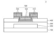
도 1을 참조하면, 트렌지스터(1)는 기판(100) 상의 게이트 전극(200), 게이트 절연막(300), 소스/드레인 전극들(400), 및 산화물 반도체층(500)을 포함할 수 있다.Referring to FIG. 1, a
게이트 전극(200)이 기판(100) 상에 배치될 수 있다. 기판(100)은 실리콘 반도체(Si, SiO2), 유리, 석영, 및/또는 폴리머를 포함하며, 대략 0.1 내지 1mm의 두께를 가질 수 있다. 게이트 전극(200)은 백금(Pt), 금(Au), 은(Ag), 알루미늄(Al), 니켈(Ni), 티타늄(Ti), 구리(Cu), 크롬(Cr), 텡스텐(W), 몰리브덴(Mo), 및 산화물 전도체(ITO, IGO 등)로 이루어진 군에서 선택되는 적어도 하나를 포함할 수 있다.A
게이트 절연막(300)이 기판(100) 상에서 제공되며, 게이트 전극(200)을 덮을 수 있다. 게이트 절연막(300)은 게이트 전극(200) 및 산화물 반도체층(500) 사이에 배치될 수 있다. 게이트 절연막(300)은 산화물 유전체, 예를 들어, Al2O3, SiO2, HfO2, Ta2O5, ZrO2, BaTiO3, SrTiO3, 및 BaSnO3중에서 선택된 적어도 하나를 포함할 수 있다.A
소스/드레인 전극들(400)이 게이트 절연막(300) 상에 배치되어, 게이트 절연막(300)의 일부를 덮을 수 있다. 소스/드레인 전극들(400)은 상기 게이트 전극(200)의 예로써 설명한 물질 중에서 적어도 하나를 포함할 수 있다.The source /
산화물 반도체층(500)이 게이트 절연막(300) 상에서 게이트 전극(200)과 대응되는 위치에 배치될 수 있다. 산화물 반도체층(500)은 소스/드레인 전극들(400) 사이에 개재될 수 있다. 산화물 반도체층(500)은 소스/드레인 전극들(400) 상으로 연장되어, 소스/드레인 전극들(400)의 가장자리를 덮을 수 있다. 산화물 반도체층(500)은 활성층으로서 트렌지스터(1)의 동작시 채널을 제공하는 역할을 할 수 있다. 산화물 반도체층(500)은 BaTiO3, SrTiO3, BaSnO3, ZnO, CuO, NiO, SnO2, TiO2, CoO, In2O3, WO3, MgO, CaO, La2O3, Nd2O3, Y2O3, CeO2, PbO, ZrO2, Fe2O3, Bi2O3, V2O5, VO2, Nb2O5, Co3O4 및 Al2O3로 이루어진 군에서 적어도 2개를 포함할 수 있다. 산화물 반도체층(500)은 나노층상 구조를 가질 수 있다. 나노 층상구조란 서로 다른 층들이 나노사이즈 두께로 적층된 구조를 의미할 수 있다. 예를 들어, 산화물 반도체층(500)은 적어도 하나의 제1 나노층(510) 및 적어도 하나의 제2 나노층(520)을 포함할 수 있다. 산화물 반도체층(500)은 1 내지 100nm의 두께를 가질 수 있다. 제1 나노층(510) 및 제2 나노층(520)은 각각 1 내지 10nm의 두께를 가질 수 있다. 제2 나노층(520)은 제1 나노층(510) 상에 배치되며, 제1 나노층(510)과 번갈아가며 적층될 수 있다. 다른 예로, 제2 나노층(520)은 제1 나노층(510)과 무작위 순서로 적층될 수 있다. 제2 나노층(520)은 제1 나노층(510)과 다른 물질을 포함할 수 있다. 예를 들어, 제1 나노층(510)은 산화물 반도체층(500)의 예로써 설명한 물질 중에서 적어도 하나를 포함하며, 제2 나노층(520)은 다른 하나를 포함할 수 있다. 제1 나노층(510) 및 제2 나노층(520)이 서로 다른 물질을 포함함에 따라, 제1 나노층(510) 및 제2 나노층(520)의 계면에서 불포화 결합(dangling bond) 및/또는 불완전한 원자배위가 제공될 수 있다. 이에 따라, 제1 나노층(510) 및 제2 나노층(520)의 계면에서 전자 이동 채널층이 형성되어 높은 전자이동도가 나타날 수 있다. 일 예로, 산화물 반도체층(500)은 InZnO를 포함할 수 있다. 산화물 반도체층(500)이 In2O3를 포함하는 제1 나노층(510) 및 ZnO를 포함하는 제2 나노층(520)이 교대로 적층되어 제공된 InZnO를 포함하는 경우, 단층 구조를 가지는 InZnO를 포함하 경우보다 더 높은 전자 이동도를 가지는 채널을 구현할 수 있다. 본 발명의 트렌지스터(1)는 높은 신뢰도를 가질 수 있다.The
도 2는 본 발명의 다른 실시예에 따른 트렌지스터를 도시한 단면도이다. 이하 도 1을 참조하여 중복되는 내용은 생략한다.2 is a cross-sectional view illustrating a transistor according to another embodiment of the present invention. Hereinafter, redundant description will be omitted with reference to FIG.
도 2를 참조하면, 트렌지스터(2)는 기판(100) 상의 게이트 전극(200), 게이트 절연막(300), 소스/드레인 전극들(400), 및 산화물 반도체층(500)을 포함할 수 있다. 게이트 전극(200), 게이트 절연막(300), 및 소스/드레인 전극들(400)은 도 1의 예로써 설명한 바와 같다.Referring to FIG. 2, the
산화물 반도체층(500)이 게이트 절연막(300) 상에서 게이트 전극(200)과 대응되는 위치에 배치될 수 있다. 산화물 반도체층(500)은 나노층상 구조를 가질 수 있다. 산화물 반도체층(500)은 적어도 하나의 제1 나노층(510), 제2 나노층(520), 및 제3 나노층(530)을 포함할 수 있다. 제2 나노층(520), 및 제3 나노층(530)이 제1 나노층(510) 상에 차례로 적층될 수 있다. 일 예로, 제1 나노층(510), 제2 나노층(520), 및 제3 나노층(530)은 번갈아가며 적층될 수 있다. 다른 예로, 제1 나노층(510), 제2 나노층(520), 및 제3 나노층(530)은 무작위로 적층될 수 있으나 이에 한정되지 않는다. 제3 나노층(530)은 제1 나노층(510) 및 제2 나노층(520)과 다른 물질을 포함할 수 있다. 예를 들어, 제3 나노층(530)은 BaTiO3, SrTiO3, BaSnO3, ZnO, CuO, NiO, SnO2, TiO2, CoO, In2O3, WO3, MgO, CaO, La2O3, Nd2O3, Y2O3, CeO2, PbO, ZrO2, Fe2O3, Bi2O3, V2O5, VO2, Nb2O5, Co3O4 및 Al2O3로 이루어진 군에서 선택된 적어도 하나를 포함할 수 있다. 산화물 반도체층(500)은 1 내지 100nm의 두께를 가질 수 있다. 제1 나노층(510), 제2 나노층(520) 및 제3 나노층(530)은 각각 1 내지 10nm의 두께를 가질 수 있다. 제1 나노층(510)과 제2 나노층(520)의 계면, 제2 나노층(520)과 제3 나노층(530)의 계면, 및/또는 제1 나노층(510)과 제3 나노층(530)의 계면에서 불포화 결합(dangling bond) 및/또는 불완전한 원자배위가 제공되어, 산화물 반도체층(500)은 높은 전하이동도를 가지는 채널을 구현할 수 있다.
The
도 3은 본 발명의 또 다른 실시예에 따른 트렌지스터를 도시한 단면도이다. 이하 앞서 설명한 바와 중복되는 내용은 생략한다.3 is a cross-sectional view illustrating a transistor according to another embodiment of the present invention. Hereinafter, the same elements as those described above will be omitted.
도 3을 참조하면, 트렌지스터(3)는 기판(100) 상의 게이트 전극(200), 게이트 절연막(300), 소스/드레인 전극들(400), 및 산화물 반도체층(500)을 포함할 수 있다. 기판(100), 게이트 전극(200) 및 게이트 절연막(300)은 도 1의 예에서 설명한 바와 동일할 수 있다. 이와 달리, 소스/드레인 전극들(400) 및 산화물 반도체층(500)은 다른 형태로도 배치될 수 있다.Referring to FIG. 3, the
산화물 반도체층(500)이 게이트 절연막(300) 상에 제공되며, 소스/드레인 전극들(400) 에 의해 일부가 덮일 수 있다. 산화물 반도체층(500)은 나노층상 구조를 가질 수 있다. 산화물 반도체층(500)은 적어도 하나의 제1 나노층(510) 및 적어도 하나의 제2 나노층(520)을 포함할 수 있다. 제1 나노층(510) 및 제2 나노층(520)은 도 1의 예로써 설명한 바와 동일하거나 유사할 수 있다. 산화물 반도체층(500)은 도 2의 예로써 설명한 제3 나노층(530)을 더 포함할 수 있으나, 이에 한정되지 않는다. 소스/드레인 전극들(400)이 게이트 절연막(300) 상에 제공될 수 있다. 소스/드레인 전극들(400)은 산화물 반도체층(500) 상으로 연장되어, 산화물 반도체층(500)의 가장자리를 덮을 수 있다.
An
도 4는 본 발명의 또 다른 실시예에 따른 트렌지스터를 도시한 단면도이다.4 is a cross-sectional view illustrating a transistor according to another embodiment of the present invention.
도 4를 참조하면, 트렌지스터(4)는 기판(100) 상의 산화물 반도체층(500), 소스/드레인 전극들(400), 게이트 절연막(300), 및 게이트 전극(200)을 포함할 수 있다.Referring to FIG. 4, the
도 4를 참조하면, 소스/드레인 전극들(400)이 기판(100) 상에 배치되어, 기판(100)의 일부를 덮을 수 있다. 산화물 반도체층(500)은 기판(100) 상에 소스/드레인 전극들(400) 사이에 개재될 수 있다. 산화물 반도체층(500)은 소스/드레인 전극들(400)의 가장자리와 접하며, 소스/드레인 전극들(400) 상으로 연장될 수 있다. 산화물 반도체층(500)은 나노층상 구조를 가질 수 있다. 산화물 반도체층(500)은 적어도 하나의 제1 나노층(510) 및 적어도 하나의 제2 나노층(520)을 포함할 수 있다. 제1 나노층(510) 및 제2 나노층(520)은 도 1의 예로써 설명한 바와 동일하거나 유사할 수 있다. 산화물 반도체층(500)은 도 2의 예로써 설명한 제3 나노층(530)을 더 포함할 수 있으나, 이에 한정되지 않는다. 게이트 절연막(300)이 산화물 반도체층(500) 및 게이트 전극(200) 사이에 개재될 수 있다. 게이트 절연막(300)은 산화물 반도체층(500)을 덮을 수 있다. 게이트 전극(200)이 게이트 절연막(300) 상에 제공되며, 산화물 반도체층(500)과 대응되는 위치에 배치될 수 있다.
Referring to FIG. 4, source /
도 5는 본 발명의 또 다른 실시예에 따른 트렌지스터를 도시한 단면도이다.5 is a cross-sectional view illustrating a transistor according to another embodiment of the present invention.
도 5를 참조하면, 트렌지스터(5)는 기판(100) 상의 산화물 반도체층(500), 소스/드레인 전극들(400), 게이트 절연막(300), 및 게이트 전극(200)을 포함할 수 있다. 기판(100), 게이트 전극(200) 및 게이트 절연막(300)은 도 4의 예에서 설명한 바와 동일할 수 있다. 이와 달리, 소스/드레인 전극들(400) 및 산화물 반도체층(500)은 다른 형태로도 배치될 수 있다.5, the transistor 5 may include an
산화물 반도체층(500)이 기판(100) 상에 배치되어, 기판(100)의 일부를 덮을 수 있다. 산화물 반도체층(500)의 일부가 소스/드레인 전극들(400)에 의하여 덮일 수 있다. 산화물 반도체층(500)은 나노층상 구조를 가질 수 있다. 산화물 반도체층(500)은 적어도 하나의 제1 나노층(510) 및 적어도 하나의 제2 나노층(520)을 포함할 수 있다. 제1 나노층(510) 및 제2 나노층(520)은 도 1의 예로써 설명한 바와 동일하거나 유사할 수 있다. 제1 나노층(510) 및 제2 나노층(520)은 번갈아가며 적층될 수 있으나, 이에 한정되지 않는다. 산화물 반도체층(500)은 도 2의 예로써 설명한 제3 나노층(미도시)을 더 포함할 수 있다. 소스/드레인 전극들(400)이 기판(100)의 일부를 덮을 수 있다. 소스/드레인 전극들(400)은 산화물 반도체층(500) 상으로 연장되어, 산화물 반도체층(500)의 가장자리를 덮을 수 있다.
The
이하, 첨부한 도면들을 참조하여 본 발명에 따른 트렌지스터의 제조방법을 설명한다.Hereinafter, a method of manufacturing a transistor according to the present invention will be described with reference to the accompanying drawings.
도 1을 다시 참조하면, 산화물 반도체층(500)이 기판(100) 상에 형성될 수 있다. 기판(100)은 도 1의 예로써 설명한 게이트 전극(200), 게이트 절연막(300), 및 소스/드레인 전극들(400)이 형성된 기판(100)일 수 있다. 제1 나노층(510)이 도 1의 예로써 설명한 물질을 기판(100) 상에 증착하여 1 내지 10nm의 두께를 가지도록 형성될 수 있다. 예를 들어, 제1 나노층(510)은 펄스레이저 증착법, 스퍼터링(sputtering), 원자층 증착(atomic layer deposition, ALD) 또는 졸-겔 법에 의하여 형성될 수 있다. 제2 나노층(520)이 도 1의 예로써 설명한 물질(BaTiO3, SrTiO3, BaSnO3, ZnO, CuO, NiO, SnO2, TiO2, CoO, In2O3, WO3, MgO, CaO, La2O3, Nd2O3, Y2O3, CeO2, PbO, ZrO2, Fe2O3, Bi2O3, V2O5, VO2, Nb2O5, Co3O4 및 Al2O3로 이루어진 군에서 선택된 적어도 하나)을 제1 나노층(510) 상에 증착하여 1 내지 10nm의 두께를 가지도록 형성될 수 있다. 제2 나노층(520)은 제1 나노층(510)과 다른 물질을 증착하여 형성될 수 있다. 제2 나노층(520)은 제1 나노층(510)의 예로써 설명한 증착법 중 어느 하나에 의하여 형성될 수 있다. 제1 나노층(510) 및 제2 나노층(520)은 반복하여 증착될 수 있다. 이 후, 제1 나노층(510) 및 제2 나노층(520)을 패터닝하여 산화물 반도체층(500)이 제조될 수 있다. 이에 따라, 본 발명의 트렌지스터(1)의 제조가 완성될 수 있다.
Referring again to FIG. 1, an
이하, 본 발명의 실험예를 참조하여, 본 발명에 따른 트렌지스터의 제조 및 상기 트렌지스터의 특성평가 결과를 보다 상세하게 설명한다.
Hereinafter, the production of the transistor according to the present invention and the evaluation result of the characteristics of the transistor will be described in more detail with reference to the experimental examples of the present invention.
트렌지스터의Of the transistor 제조 Produce
<실험예><Experimental Example>
(산화물 반도체층의 제조)(Preparation of oxide semiconductor layer)
펄스레이저 증착법을 사용하여 나노 층상구조의 ZnSnO 산화물 반도체 박막을 제조하였다. ZnO타겟을 사용한 펄스레이저 증착법에 의하여 0.8nm의 두께를 가지는 ZnO나노박막이 증착될 수 있다. ZnO박막 상에 SnO2타겟을 사용한 펄스레이저 증착법에 의하여 0.8nm의 두께를 가지는 SnO2나노박막이 증착될 수 있다. ZnO와 SnO2 나노박막을 교대로 반복하여 증착하여 나노 층상구조가 형성할 수 있다. 예를 들어, ZnO와 SnO2 나노 박막은 20층의 나노 층상구조를 가지도록 반복적으로 증착될 수 있다. 이에 따라, 나노 층상구조의 ZnSnO산화물 반도체층의 제조가 완성될 수 있다. 나노 층상 구조의 ZnSnO산화물 반도체층은 32nm의 두께를 가지도록 형성될 수 있다.A nano - layered ZnSnO oxide semiconductor thin film was fabricated by pulsed laser deposition. ZnO nanotubes having a thickness of 0.8 nm can be deposited by pulsed laser deposition using a ZnO target. On the ZnO thin film, SnO2 A SnO2 nano thin film having a thickness of 0.8 nm can be deposited by pulsed laser deposition using a target. ZnO and SnO2 nanotubes may be alternately deposited repeatedly to form a nano-layered structure. For example, ZnO and SnO2 nanotubes can be repeatedly deposited to have a 20-layer nano-layer structure. Thus, the production of a ZnSnO oxide semiconductor layer having a nano-layer structure can be completed. The nano-layered ZnSnO oxide semiconductor layer may be formed to have a thickness of 32 nm.
(트렌지스터의 제조)(Manufacture of a transistor)
산화물 반도체층이 형성된 유리기판이 제공될 수 있다. 산화물 반도체층은 앞서 설명한 나노 층상구조의 ZnSnO 산화물 반도체층일 수 있다. 유리기판 상에 ITO로부터 게이트 전극(ITO), 게이트 절연막(Al2O3), 소스/드레인 전극(ITO)을 형성하여, 도 5의 구조를 가지는 트렌지스터(5)가 제조될 수 있다.
A glass substrate on which an oxide semiconductor layer is formed may be provided. The oxide semiconductor layer may be a ZnSnO oxide semiconductor layer having the nano-layer structure as described above. A transistor 5 having the structure of FIG. 5 can be manufactured by forming a gate electrode (ITO), a gate insulating film (Al2 O3 ), and a source / drain electrode (ITO) from ITO on a glass substrate.
트렌지스터의Of the transistor 특성 평가 결과 Characteristic evaluation result
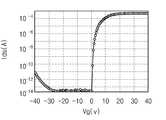
도 6은 실험예의 나노층상 구조의 ZnSnO 박막을 사용하여 제조한 트랜지스터의 전송특성을 평가한 그래프이다. 전송특성은 소스/드레인 전극 사이에 15V의 드레인 전압(Vd) 하에서 게이트 전압(Vg)에 따른 드레인 전류(Ids)를 측정하였다. 이하 도 5를 함께 참조하여 설명한다.FIG. 6 is a graph illustrating a transmission characteristic of a transistor manufactured using a ZnSnO thin film having a nano-layer structure according to an experimental example. The transfer characteristics measured the drain current (Ids) according to the gate voltage (Vg) under a drain voltage (Vd) of 15 V between the source / drain electrodes. Hereinafter, Fig. 5 will be described together.
도 6을 참조하면, 실험예는 16.4 cm2/Vs의 포화 전자 이동도(msat)를 가지는 것을 관찰할 수 있다. 실험예는 108이상의 Ion/Ioff 전류비를, 0.25 V/dec의 문턱전압 이하에서의 기울기 값(Subthreshold swing, ss)을 가진다. 실험예는 제1 나노층(510) 및 제1 나노층(510)과 다른 물질을 포함하는 제2 나노층(520)을 포함함에 따라, 제1 나노층(510) 및 제2 나노층(520)의 계면에서 높은 전자이동도가 나타날 수 있다. 이에 따라, 트렌지스터(5)는 양호한 전송특성을 나타낼 수 있다.
Referring to FIG. 6, it can be seen that the experimental example has a saturation electron mobility (msat ) of 16.4 cm2 / Vs. The experimental example has an Ion / Ioff current ratio of 108 or more and a slope value (subthreshold swing, ss) at a threshold voltage of 0.25 V / dec or less. Experimental examples include a
이상, 본 발명을 바람직한 실시예를 들어 상세하게 설명하였으나, 본 발명은 상기 실시예에 한정되지 않고, 본 발명의 기술적 사상 및 범위 내에서 당 분야에서 통상의 지식을 가진 자에 의하여 여러 가지 변형 및 변경이 가능하다.While the present invention has been particularly shown and described with reference to exemplary embodiments thereof, it is to be understood that the present invention is not limited to the disclosed exemplary embodiments, and various changes and modifications may be made by those skilled in the art without departing from the scope and spirit of the invention. Change is possible.
Claims (10)
Translated fromKorean상기 소스/드레인 전극들 사이의 반도체 산화물층;
상기 반도체 산화물층에 대응하는 게이트 전극; 및
상기 반도체 산화물층 및 게이트 전극 사이에 개재된 게이트 절연막을 포함하되,
상기 반도체 산화물층은 나노 층상구조를 가지며, 적어도 하나의 제1 나노층 및 적어도 하나의 제2 나노층을 포함하고,
상기 제2 나노층은 상기 제1 나노층 상에 제공되며, 상기 제1 나노층과 다른 물질을 포함하고,
상기 제1 나노층 및 상기 제2 나노층 사이의 계면에 불포화 결합(dangling bond) 및 불완전한 원자배위 중에서 적어도 하나가 제공되어, 상기 계면에서 전자 이동 채널층이 제공되는 트렌지스터.
Source / drain electrodes on the substrate;
A semiconductor oxide layer between the source / drain electrodes;
A gate electrode corresponding to the semiconductor oxide layer; And
And a gate insulating film interposed between the semiconductor oxide layer and the gate electrode,
Wherein the semiconductor oxide layer has a nano-layer structure and includes at least one first nanolayer and at least one second nanolayer,
Wherein the second nanolayer is provided on the first nanolayer and comprises a material different from the first nanolayer,
Wherein at least one of a dangling bond and an imperfect atomic coordination is provided at an interface between the first nanolayer and the second nanolayer to provide an electron transport channel layer at the interface.
상기 제1 나노층 및 상기 제2 나노층은 번갈아가며 적층되는 트렌지스터.
The method according to claim 1,
Wherein the first nano layer and the second nano layer are alternately stacked.
상기 제1 나노층은 BaTiO3, SrTiO3, BaSnO3, ZnO, CuO, NiO, SnO2, TiO2, CoO, In2O3, WO3, MgO, CaO, La2O3, Nd2O3, Y2O3, CeO2, PbO, ZrO2, Fe2O3, Bi2O3, V2O5, VO2, Nb2O5, Co3O4 및 Al2O3로 이루어진 군에서 선택된 하나를 포함하며,
상기 제2 나노층은 BaTiO3, SrTiO3, BaSnO3, ZnO, CuO, NiO, SnO2, TiO2, CoO, In2O3, WO3, MgO, CaO, La2O3, Nd2O3, Y2O3, CeO2, PbO, ZrO2, Fe2O3, Bi2O3, V2O5, VO2, Nb2O5, Co3O4 및 Al2O3로 이루어진 군에서 선택된 다른 하나를 포함하는 트렌지스터.
The method according to claim 1,
The first nano-layer may be formed of BaTiO3 , SrTiO3 , BaSnO3 , ZnO, CuO, NiO, SnO2 , TiO2 , CoO, In2 O3 , WO3 , MgO, CaO, La2 O3 , Nd2 O3 , Y2 O3 , CeO2 , PbO, ZrO2 , Fe2 O3 , Bi2 O3 , V2 O5 , VO2 , Nb2 O5 , Co3 O4 and Al2 O3 Selected < / RTI >
The second nano-layer may be formed of BaTiO3 , SrTiO3 , BaSnO3 , ZnO, CuO, NiO, SnO2 , TiO2 , CoO, In2 O3 , WO3 , MgO, CaO, La2 O3 , Nd2 O3 , Y2 O3 , CeO2 , PbO, ZrO2 , Fe2 O3 , Bi2 O3 , V2 O5 , VO2 , Nb2 O5 , Co3 O4 and Al2 O3 A transistor comprising another selected one.
상기 반도체 산화물층은 상기 제2 나노층 상의 제3 나노층을 더 포함하되,
상기 제3 나노층은 상기 제1 나노층 및 상기 제2 나노층과 다른 물질을 포함하는 트렌지스터.
The method according to claim 1,
Wherein the semiconductor oxide layer further comprises a third nanolayer on the second nanolayer,
Wherein the third nanolayer comprises a material different from the first nanolayer and the second nanolayer.
상기 제1 나노층, 상기 제2 나노층, 및 상기 제3 나노층은 번갈아가며 적층되는 트렌지스터.
6. The method of claim 5,
Wherein the first nano layer, the second nano layer, and the third nano layer are alternately stacked.
상기 반도체 산화물층은 0.1 내지 100nm의 두께를 가지는 트렌지스터.
The method according to claim 1,
Wherein the semiconductor oxide layer has a thickness of 0.1 to 100 nm.
상기 제1 나노층 상에 상기 제1 나노층과 다른 물질을 포함하는 제2 나노층을 형성하는 것; 그리고
상기 기판 상에 소스/드레인 전극, 게이트 절연막, 및 게이트 전극을 형성하는 것을 포함하되,
상기 제1 나노층 및 상기 제2 나노층 사이의 계면에 불포화 결합 및 불완전한 원자배위 중에서 적어도 하나가 제공되어, 상기 계면에서 전자 이동 채널층이 형성되는 트렌지스터 제조방법.
Forming a first nanolayer including an oxide semiconductor on a substrate;
Forming a second nano-layer on the first nano-layer including a material different from the first nano-layer; And
Forming a source / drain electrode, a gate insulating film, and a gate electrode on the substrate,
Wherein at least one of an unsaturated bond and an imperfect atomic coordination is provided at an interface between the first nano layer and the second nano layer to form an electron transport channel layer at the interface.
상기 제2 나노층 상에 제3 나노층을 형성하는 것을 더 포함하되,
상기 제3 나노층은 상기 제1 나노층 및 상기 제2 나노층과 다른 물질을 포함하는 트렌지스터 제조방법.
9. The method of claim 8,
Further comprising forming a third nanolayer on the second nanolayer,
Wherein the third nanolayer comprises a material different from the first nanolayer and the second nanolayer.
상기 제1 나노층은 BaTiO3, SrTiO3, BaSnO3, ZnO, CuO, NiO, SnO2, TiO2, CoO, In2O3, WO3, MgO, CaO, La2O3, Nd2O3, Y2O3, CeO2, PbO, ZrO2, Fe2O3, Bi2O3, V2O5, VO2, Nb2O5, Co3O4 및 Al2O3로 이루어진 군에서 선택된 하나를 포함하며,
상기 제2 나노층은 BaTiO3, SrTiO3, BaSnO3, ZnO, CuO, NiO, SnO2, TiO2, CoO, In2O3, WO3, MgO, CaO, La2O3, Nd2O3, Y2O3, CeO2, PbO, ZrO2, Fe2O3, Bi2O3, V2O5, VO2, Nb2O5, Co3O4 및 Al2O3로 이루어진 군에서 선택된 다른 하나를 포함하는 트렌지스터 제조방법.9. The method of claim 8,
The first nano-layer may be formed of BaTiO3 , SrTiO3 , BaSnO3 , ZnO, CuO, NiO, SnO2 , TiO2 , CoO, In2 O3 , WO3 , MgO, CaO, La2 O3 , Nd2 O3 , Y2 O3 , CeO2 , PbO, ZrO2 , Fe2 O3 , Bi2 O3 , V2 O5 , VO2 , Nb2 O5 , Co3 O4 and Al2 O3 Selected < / RTI >
The second nano-layer may be formed of BaTiO3 , SrTiO3 , BaSnO3 , ZnO, CuO, NiO, SnO2 , TiO2 , CoO, In2 O3 , WO3 , MgO, CaO, La2 O3 , Nd2 O3 , Y2 O3 , CeO2 , PbO, ZrO2 , Fe2 O3 , Bi2 O3 , V2 O5 , VO2 , Nb2 O5 , Co3 O4 and Al2 O3 And the other one selected.
Priority Applications (2)
| Application Number | Priority Date | Filing Date | Title |
|---|---|---|---|
| KR1020120144276AKR101943077B1 (en) | 2012-12-12 | 2012-12-12 | A transistor hanving nano layer structured oxides and method of manufacturing the same |
| US14/020,498US9263592B2 (en) | 2012-12-12 | 2013-09-06 | Oxide transistor with nano-layered structure |
Applications Claiming Priority (1)
| Application Number | Priority Date | Filing Date | Title |
|---|---|---|---|
| KR1020120144276AKR101943077B1 (en) | 2012-12-12 | 2012-12-12 | A transistor hanving nano layer structured oxides and method of manufacturing the same |
Publications (2)
| Publication Number | Publication Date |
|---|---|
| KR20140076111A KR20140076111A (en) | 2014-06-20 |
| KR101943077B1true KR101943077B1 (en) | 2019-04-17 |
Family
ID=50879975
Family Applications (1)
| Application Number | Title | Priority Date | Filing Date |
|---|---|---|---|
| KR1020120144276AExpired - Fee RelatedKR101943077B1 (en) | 2012-12-12 | 2012-12-12 | A transistor hanving nano layer structured oxides and method of manufacturing the same |
Country Status (2)
| Country | Link |
|---|---|
| US (1) | US9263592B2 (en) |
| KR (1) | KR101943077B1 (en) |
Families Citing this family (6)
| Publication number | Priority date | Publication date | Assignee | Title |
|---|---|---|---|---|
| KR20160115076A (en) | 2015-03-25 | 2016-10-06 | 서울대학교산학협력단 | BaSnO3 thin film transistor with high field-effect mobility and producing method thereof |
| KR101914835B1 (en)* | 2016-11-18 | 2018-11-02 | 아주대학교산학협력단 | Metal oxide heterojunction structure, method of manufacturing the metal oxide heterojunction structure, and thin film transistor having the metal oxide heterojunction structure |
| US10868191B2 (en) | 2018-12-07 | 2020-12-15 | Cornell University | Patterning electronic devices using reactive-ion etching of tin oxides |
| CN109950319B (en)* | 2019-03-04 | 2020-07-14 | 华东师范大学 | Vacuum gauge and working method thereof |
| US12342566B2 (en) | 2019-09-11 | 2025-06-24 | Seoul National University R&Db Foundation | Two-dimensional electron gas at interface between BASNO3 and LAINO3 |
| US11973141B2 (en) | 2021-08-09 | 2024-04-30 | International Business Machines Corporation | Nanosheet transistor with ferroelectric region |
Citations (4)
| Publication number | Priority date | Publication date | Assignee | Title |
|---|---|---|---|---|
| US20080296650A1 (en) | 2007-06-04 | 2008-12-04 | Micron Technology, Inc. | High-k dielectrics with gold nano-particles |
| JP2010515828A (en) | 2007-01-11 | 2010-05-13 | スリーエム イノベイティブ プロパティズ カンパニー | Thin-film electronic device and electronic circuit manufacturing apparatus and manufacturing method |
| US20120012840A1 (en) | 2009-03-31 | 2012-01-19 | Vincent Korthuis | Thin-film Transistor (TFT) With A Bi-layer Channel |
| US20130256653A1 (en) | 2012-04-02 | 2013-10-03 | Samsung Display Co., Ltd. | Thin film transistor having plural semiconductive oxides, thin film transistor array panel and display device including the same, and manufacturing method of thin film transistor |
Family Cites Families (4)
| Publication number | Priority date | Publication date | Assignee | Title |
|---|---|---|---|---|
| KR101600051B1 (en)* | 2009-03-23 | 2016-03-07 | 삼성전자주식회사 | Oxide Semiconductor and Thin Film Transistor comprising the same |
| KR101669953B1 (en)* | 2010-03-26 | 2016-11-09 | 삼성전자 주식회사 | Oxide thin film and method of forming the oxide thin film and an electronic device including the oxide thin film |
| KR101778224B1 (en)* | 2010-10-12 | 2017-09-15 | 삼성전자주식회사 | Transistor, method of manufacturing the same and electronic device comprising transistor |
| KR101198874B1 (en)* | 2010-11-24 | 2012-11-07 | 연세대학교 산학협력단 | Method of improving performance of carbon nano tube for transparent metal oxide thin film field effect transistor and the same transistor |
- 2012
- 2012-12-12KRKR1020120144276Apatent/KR101943077B1/ennot_activeExpired - Fee Related
- 2013
- 2013-09-06USUS14/020,498patent/US9263592B2/ennot_activeExpired - Fee Related
Patent Citations (4)
| Publication number | Priority date | Publication date | Assignee | Title |
|---|---|---|---|---|
| JP2010515828A (en) | 2007-01-11 | 2010-05-13 | スリーエム イノベイティブ プロパティズ カンパニー | Thin-film electronic device and electronic circuit manufacturing apparatus and manufacturing method |
| US20080296650A1 (en) | 2007-06-04 | 2008-12-04 | Micron Technology, Inc. | High-k dielectrics with gold nano-particles |
| US20120012840A1 (en) | 2009-03-31 | 2012-01-19 | Vincent Korthuis | Thin-film Transistor (TFT) With A Bi-layer Channel |
| US20130256653A1 (en) | 2012-04-02 | 2013-10-03 | Samsung Display Co., Ltd. | Thin film transistor having plural semiconductive oxides, thin film transistor array panel and display device including the same, and manufacturing method of thin film transistor |
Also Published As
| Publication number | Publication date |
|---|---|
| KR20140076111A (en) | 2014-06-20 |
| US20140159036A1 (en) | 2014-06-12 |
| US9263592B2 (en) | 2016-02-16 |
Similar Documents
| Publication | Publication Date | Title |
|---|---|---|
| KR101943077B1 (en) | A transistor hanving nano layer structured oxides and method of manufacturing the same | |
| TWI612584B (en) | Field effect transistor manufacturing method and field effect transistor | |
| KR101675113B1 (en) | Transistor and method of manufacturing the same | |
| JP5434000B2 (en) | Field effect transistor and manufacturing method thereof | |
| US8466462B2 (en) | Thin film transistor and method of fabricating the same | |
| KR101016266B1 (en) | Transparent memory for transparent electronic devices. | |
| TWI493723B (en) | Thin film transistor, method and device for manufacturing thin film transistor | |
| JP2013030681A (en) | Method of manufacturing semiconductor element, and method of manufacturing field-effect transistor | |
| TW200915577A (en) | Manufacturing method of thin film transistor using oxide semiconductor | |
| JP2010186860A (en) | Field effect transistor, and method of manufacturing the same | |
| JP2009010348A (en) | Channel layer and method for forming the same, thin film transistor including the channel layer, and method for manufacturing the same | |
| KR20190129223A (en) | Oxide semiconductor thin film photo transistor and method of manufacturing the same | |
| KR20140144388A (en) | Thin film transistor array panel | |
| US20220293591A1 (en) | Electronic circuits and circuit elements | |
| JP6121149B2 (en) | Oxide semiconductor element, manufacturing method of oxide semiconductor element, display device, and image sensor | |
| US12432982B2 (en) | Multi-channel transistor and manufacturing method by the same | |
| KR102385114B1 (en) | Multi-channel thin film transistor and manufacturing method by the same | |
| KR20110080118A (en) | A thin film transistor having a multilayer etch stop layer and a method of manufacturing the same | |
| CN108346702A (en) | Thin film transistor (TFT) and its active layer and application | |
| CN111129150B (en) | Ferroelectric thin film transistor and manufacturing method thereof | |
| KR101249091B1 (en) | Thin film transistor having enhanced charge carrier mobility and method for manufacturing the same | |
| KR101318418B1 (en) | Thin film transistor and the manufacturing method thereof | |
| KR102537352B1 (en) | Thin film trnasistor having doped oxide semiconductor layer, method for manufacturing the same and display device comprising the same | |
| CN120018578A (en) | Semiconductor devices | |
| CN119605351A (en) | Array substrate and display device |
Legal Events
| Date | Code | Title | Description |
|---|---|---|---|
| PA0109 | Patent application | St.27 status event code:A-0-1-A10-A12-nap-PA0109 | |
| P11-X000 | Amendment of application requested | St.27 status event code:A-2-2-P10-P11-nap-X000 | |
| P13-X000 | Application amended | St.27 status event code:A-2-2-P10-P13-nap-X000 | |
| PG1501 | Laying open of application | St.27 status event code:A-1-1-Q10-Q12-nap-PG1501 | |
| R17-X000 | Change to representative recorded | St.27 status event code:A-3-3-R10-R17-oth-X000 | |
| PN2301 | Change of applicant | St.27 status event code:A-3-3-R10-R13-asn-PN2301 St.27 status event code:A-3-3-R10-R11-asn-PN2301 | |
| A201 | Request for examination | ||
| P11-X000 | Amendment of application requested | St.27 status event code:A-2-2-P10-P11-nap-X000 | |
| P13-X000 | Application amended | St.27 status event code:A-2-2-P10-P13-nap-X000 | |
| PA0201 | Request for examination | St.27 status event code:A-1-2-D10-D11-exm-PA0201 | |
| PE0902 | Notice of grounds for rejection | St.27 status event code:A-1-2-D10-D21-exm-PE0902 | |
| P11-X000 | Amendment of application requested | St.27 status event code:A-2-2-P10-P11-nap-X000 | |
| P13-X000 | Application amended | St.27 status event code:A-2-2-P10-P13-nap-X000 | |
| E902 | Notification of reason for refusal | ||
| PE0902 | Notice of grounds for rejection | St.27 status event code:A-1-2-D10-D21-exm-PE0902 | |
| E13-X000 | Pre-grant limitation requested | St.27 status event code:A-2-3-E10-E13-lim-X000 | |
| P11-X000 | Amendment of application requested | St.27 status event code:A-2-2-P10-P11-nap-X000 | |
| P13-X000 | Application amended | St.27 status event code:A-2-2-P10-P13-nap-X000 | |
| E701 | Decision to grant or registration of patent right | ||
| PE0701 | Decision of registration | St.27 status event code:A-1-2-D10-D22-exm-PE0701 | |
| GRNT | Written decision to grant | ||
| PR0701 | Registration of establishment | St.27 status event code:A-2-4-F10-F11-exm-PR0701 | |
| PR1002 | Payment of registration fee | St.27 status event code:A-2-2-U10-U11-oth-PR1002 Fee payment year number:1 | |
| PG1601 | Publication of registration | St.27 status event code:A-4-4-Q10-Q13-nap-PG1601 | |
| PC1903 | Unpaid annual fee | St.27 status event code:A-4-4-U10-U13-oth-PC1903 Not in force date:20220123 Payment event data comment text:Termination Category : DEFAULT_OF_REGISTRATION_FEE | |
| PC1903 | Unpaid annual fee | St.27 status event code:N-4-6-H10-H13-oth-PC1903 Ip right cessation event data comment text:Termination Category : DEFAULT_OF_REGISTRATION_FEE Not in force date:20220123 | |
| P22-X000 | Classification modified | St.27 status event code:A-4-4-P10-P22-nap-X000 |