KR101942489B1 - Thin film transistor array panel and organic light emitting diode display including the same - Google Patents
Thin film transistor array panel and organic light emitting diode display including the sameDownload PDFInfo
- Publication number
- KR101942489B1 KR101942489B1KR1020120115358AKR20120115358AKR101942489B1KR 101942489 B1KR101942489 B1KR 101942489B1KR 1020120115358 AKR1020120115358 AKR 1020120115358AKR 20120115358 AKR20120115358 AKR 20120115358AKR 101942489 B1KR101942489 B1KR 101942489B1
- Authority
- KR
- South Korea
- Prior art keywords
- insulating film
- transistor
- electrode
- signal line
- interlayer insulating
- Prior art date
- Legal status (The legal status is an assumption and is not a legal conclusion. Google has not performed a legal analysis and makes no representation as to the accuracy of the status listed.)
- Active
Links
- 239000010409thin filmSubstances0.000titleabstractdescription46
- 239000011229interlayerSubstances0.000claimsabstractdescription52
- 239000000758substrateSubstances0.000claimsabstractdescription29
- 239000003990capacitorSubstances0.000claimsdescription42
- 239000004020conductorSubstances0.000claimsdescription40
- 239000010410layerSubstances0.000claimsdescription35
- 239000000463materialSubstances0.000claimsdescription11
- 238000000034methodMethods0.000claimsdescription9
- 239000010408filmSubstances0.000abstractdescription69
- 239000004065semiconductorSubstances0.000abstractdescription42
- 239000010936titaniumSubstances0.000description14
- 239000011810insulating materialSubstances0.000description12
- 229910052751metalInorganic materials0.000description12
- 239000002184metalSubstances0.000description12
- VYPSYNLAJGMNEJ-UHFFFAOYSA-NSilicium dioxideChemical compoundO=[Si]=OVYPSYNLAJGMNEJ-UHFFFAOYSA-N0.000description11
- RTAQQCXQSZGOHL-UHFFFAOYSA-NTitaniumChemical compound[Ti]RTAQQCXQSZGOHL-UHFFFAOYSA-N0.000description8
- 229910052814silicon oxideInorganic materials0.000description8
- 229910052719titaniumInorganic materials0.000description8
- 229910052581Si3N4Inorganic materials0.000description6
- 239000011651chromiumSubstances0.000description6
- APFVFJFRJDLVQX-UHFFFAOYSA-Nindium atomChemical compound[In]APFVFJFRJDLVQX-UHFFFAOYSA-N0.000description6
- 150000002739metalsChemical class0.000description6
- HQVNEWCFYHHQES-UHFFFAOYSA-Nsilicon nitrideChemical compoundN12[Si]34N5[Si]62N3[Si]51N64HQVNEWCFYHHQES-UHFFFAOYSA-N0.000description6
- 229910052782aluminiumInorganic materials0.000description5
- XAGFODPZIPBFFR-UHFFFAOYSA-NaluminiumChemical compound[Al]XAGFODPZIPBFFR-UHFFFAOYSA-N0.000description5
- 239000010949copperSubstances0.000description5
- RYGMFSIKBFXOCR-UHFFFAOYSA-NCopperChemical compound[Cu]RYGMFSIKBFXOCR-UHFFFAOYSA-N0.000description4
- ZOKXTWBITQBERF-UHFFFAOYSA-NMolybdenumChemical compound[Mo]ZOKXTWBITQBERF-UHFFFAOYSA-N0.000description4
- ATJFFYVFTNAWJD-UHFFFAOYSA-NTinChemical compound[Sn]ATJFFYVFTNAWJD-UHFFFAOYSA-N0.000description4
- 229910021417amorphous siliconInorganic materials0.000description4
- 229910052802copperInorganic materials0.000description4
- 238000010586diagramMethods0.000description4
- 229910052738indiumInorganic materials0.000description4
- 229910052750molybdenumInorganic materials0.000description4
- 239000011733molybdenumSubstances0.000description4
- 229910021420polycrystalline siliconInorganic materials0.000description4
- 239000002356single layerSubstances0.000description4
- JBQYATWDVHIOAR-UHFFFAOYSA-NtellanylidenegermaniumChemical compound[Te]=[Ge]JBQYATWDVHIOAR-UHFFFAOYSA-N0.000description4
- 229910000838Al alloyInorganic materials0.000description3
- VYZAMTAEIAYCRO-UHFFFAOYSA-NChromiumChemical compound[Cr]VYZAMTAEIAYCRO-UHFFFAOYSA-N0.000description3
- BQCADISMDOOEFD-UHFFFAOYSA-NSilverChemical compound[Ag]BQCADISMDOOEFD-UHFFFAOYSA-N0.000description3
- XLOMVQKBTHCTTD-UHFFFAOYSA-NZinc monoxideChemical compound[Zn]=OXLOMVQKBTHCTTD-UHFFFAOYSA-N0.000description3
- 229910052804chromiumInorganic materials0.000description3
- 238000002347injectionMethods0.000description3
- 239000007924injectionSubstances0.000description3
- 238000004519manufacturing processMethods0.000description3
- 238000001039wet etchingMethods0.000description3
- YVTHLONGBIQYBO-UHFFFAOYSA-Nzinc indium(3+) oxygen(2-)Chemical compound[O--].[Zn++].[In+3]YVTHLONGBIQYBO-UHFFFAOYSA-N0.000description3
- GYHNNYVSQQEPJS-UHFFFAOYSA-NGalliumChemical compound[Ga]GYHNNYVSQQEPJS-UHFFFAOYSA-N0.000description2
- XUIMIQQOPSSXEZ-UHFFFAOYSA-NSiliconChemical compound[Si]XUIMIQQOPSSXEZ-UHFFFAOYSA-N0.000description2
- 239000011575calciumSubstances0.000description2
- 230000007423decreaseEffects0.000description2
- 229910052733galliumInorganic materials0.000description2
- 239000011521glassSubstances0.000description2
- 239000010931goldSubstances0.000description2
- HRHKULZDDYWVBE-UHFFFAOYSA-Nindium;oxozinc;tinChemical compound[In].[Sn].[Zn]=OHRHKULZDDYWVBE-UHFFFAOYSA-N0.000description2
- 239000004973liquid crystal related substanceSubstances0.000description2
- 239000011777magnesiumSubstances0.000description2
- 229910044991metal oxideInorganic materials0.000description2
- 150000004706metal oxidesChemical class0.000description2
- NQBRDZOHGALQCB-UHFFFAOYSA-NoxoindiumChemical compound[O].[In]NQBRDZOHGALQCB-UHFFFAOYSA-N0.000description2
- KYKLWYKWCAYAJY-UHFFFAOYSA-Noxotin;zincChemical compound[Zn].[Sn]=OKYKLWYKWCAYAJY-UHFFFAOYSA-N0.000description2
- 230000003071parasitic effectEffects0.000description2
- 230000000704physical effectEffects0.000description2
- 239000004033plasticSubstances0.000description2
- 229910052710siliconInorganic materials0.000description2
- 239000010703siliconSubstances0.000description2
- 229910052709silverInorganic materials0.000description2
- 239000004332silverSubstances0.000description2
- 238000004544sputter depositionMethods0.000description2
- 229910052715tantalumInorganic materials0.000description2
- GUVRBAGPIYLISA-UHFFFAOYSA-Ntantalum atomChemical compound[Ta]GUVRBAGPIYLISA-UHFFFAOYSA-N0.000description2
- OGIDPMRJRNCKJF-UHFFFAOYSA-Ntitanium(II) oxideChemical compound[Ti]=OOGIDPMRJRNCKJF-UHFFFAOYSA-N0.000description2
- 229910001316Ag alloyInorganic materials0.000description1
- OYPRJOBELJOOCE-UHFFFAOYSA-NCalciumChemical compound[Ca]OYPRJOBELJOOCE-UHFFFAOYSA-N0.000description1
- 229910000881Cu alloyInorganic materials0.000description1
- WHXSMMKQMYFTQS-UHFFFAOYSA-NLithiumChemical compound[Li]WHXSMMKQMYFTQS-UHFFFAOYSA-N0.000description1
- FYYHWMGAXLPEAU-UHFFFAOYSA-NMagnesiumChemical compound[Mg]FYYHWMGAXLPEAU-UHFFFAOYSA-N0.000description1
- 229910001182Mo alloyInorganic materials0.000description1
- 239000004642PolyimideSubstances0.000description1
- 230000015572biosynthetic processEffects0.000description1
- 229910052791calciumInorganic materials0.000description1
- 239000000919ceramicSubstances0.000description1
- 239000013078crystalSubstances0.000description1
- ZGHDMISTQPRNRG-UHFFFAOYSA-NdimolybdenumChemical compound[Mo]#[Mo]ZGHDMISTQPRNRG-UHFFFAOYSA-N0.000description1
- PCHJSUWPFVWCPO-UHFFFAOYSA-NgoldChemical compound[Au]PCHJSUWPFVWCPO-UHFFFAOYSA-N0.000description1
- 229910052737goldInorganic materials0.000description1
- 239000012535impuritySubstances0.000description1
- AMGQUBHHOARCQH-UHFFFAOYSA-Nindium;oxotinChemical compound[In].[Sn]=OAMGQUBHHOARCQH-UHFFFAOYSA-N0.000description1
- 229910010272inorganic materialInorganic materials0.000description1
- 239000011147inorganic materialSubstances0.000description1
- 229910052744lithiumInorganic materials0.000description1
- 229910052749magnesiumInorganic materials0.000description1
- 229920000058polyacrylatePolymers0.000description1
- 229920001721polyimidePolymers0.000description1
- 239000010453quartzSubstances0.000description1
- 239000011347resinSubstances0.000description1
- 229920005989resinPolymers0.000description1
- 239000000377silicon dioxideSubstances0.000description1
- 239000010935stainless steelSubstances0.000description1
- 229910001220stainless steelInorganic materials0.000description1
- 238000002834transmittanceMethods0.000description1
Images


Classifications
- H—ELECTRICITY
- H10—SEMICONDUCTOR DEVICES; ELECTRIC SOLID-STATE DEVICES NOT OTHERWISE PROVIDED FOR
- H10D—INORGANIC ELECTRIC SEMICONDUCTOR DEVICES
- H10D86/00—Integrated devices formed in or on insulating or conducting substrates, e.g. formed in silicon-on-insulator [SOI] substrates or on stainless steel or glass substrates
- H10D86/40—Integrated devices formed in or on insulating or conducting substrates, e.g. formed in silicon-on-insulator [SOI] substrates or on stainless steel or glass substrates characterised by multiple TFTs
- H10D86/60—Integrated devices formed in or on insulating or conducting substrates, e.g. formed in silicon-on-insulator [SOI] substrates or on stainless steel or glass substrates characterised by multiple TFTs wherein the TFTs are in active matrices
- H—ELECTRICITY
- H10—SEMICONDUCTOR DEVICES; ELECTRIC SOLID-STATE DEVICES NOT OTHERWISE PROVIDED FOR
- H10D—INORGANIC ELECTRIC SEMICONDUCTOR DEVICES
- H10D86/00—Integrated devices formed in or on insulating or conducting substrates, e.g. formed in silicon-on-insulator [SOI] substrates or on stainless steel or glass substrates
- H10D86/40—Integrated devices formed in or on insulating or conducting substrates, e.g. formed in silicon-on-insulator [SOI] substrates or on stainless steel or glass substrates characterised by multiple TFTs
- H10D86/421—Integrated devices formed in or on insulating or conducting substrates, e.g. formed in silicon-on-insulator [SOI] substrates or on stainless steel or glass substrates characterised by multiple TFTs having a particular composition, shape or crystalline structure of the active layer
- H10D86/423—Integrated devices formed in or on insulating or conducting substrates, e.g. formed in silicon-on-insulator [SOI] substrates or on stainless steel or glass substrates characterised by multiple TFTs having a particular composition, shape or crystalline structure of the active layer comprising semiconductor materials not belonging to the Group IV, e.g. InGaZnO
- G—PHYSICS
- G02—OPTICS
- G02F—OPTICAL DEVICES OR ARRANGEMENTS FOR THE CONTROL OF LIGHT BY MODIFICATION OF THE OPTICAL PROPERTIES OF THE MEDIA OF THE ELEMENTS INVOLVED THEREIN; NON-LINEAR OPTICS; FREQUENCY-CHANGING OF LIGHT; OPTICAL LOGIC ELEMENTS; OPTICAL ANALOGUE/DIGITAL CONVERTERS
- G02F1/00—Devices or arrangements for the control of the intensity, colour, phase, polarisation or direction of light arriving from an independent light source, e.g. switching, gating or modulating; Non-linear optics
- G02F1/01—Devices or arrangements for the control of the intensity, colour, phase, polarisation or direction of light arriving from an independent light source, e.g. switching, gating or modulating; Non-linear optics for the control of the intensity, phase, polarisation or colour
- G02F1/13—Devices or arrangements for the control of the intensity, colour, phase, polarisation or direction of light arriving from an independent light source, e.g. switching, gating or modulating; Non-linear optics for the control of the intensity, phase, polarisation or colour based on liquid crystals, e.g. single liquid crystal display cells
- G02F1/133—Constructional arrangements; Operation of liquid crystal cells; Circuit arrangements
- G02F1/136—Liquid crystal cells structurally associated with a semi-conducting layer or substrate, e.g. cells forming part of an integrated circuit
- G02F1/1362—Active matrix addressed cells
- G02F1/136213—Storage capacitors associated with the pixel electrode
- G—PHYSICS
- G02—OPTICS
- G02F—OPTICAL DEVICES OR ARRANGEMENTS FOR THE CONTROL OF LIGHT BY MODIFICATION OF THE OPTICAL PROPERTIES OF THE MEDIA OF THE ELEMENTS INVOLVED THEREIN; NON-LINEAR OPTICS; FREQUENCY-CHANGING OF LIGHT; OPTICAL LOGIC ELEMENTS; OPTICAL ANALOGUE/DIGITAL CONVERTERS
- G02F1/00—Devices or arrangements for the control of the intensity, colour, phase, polarisation or direction of light arriving from an independent light source, e.g. switching, gating or modulating; Non-linear optics
- G02F1/01—Devices or arrangements for the control of the intensity, colour, phase, polarisation or direction of light arriving from an independent light source, e.g. switching, gating or modulating; Non-linear optics for the control of the intensity, phase, polarisation or colour
- G02F1/13—Devices or arrangements for the control of the intensity, colour, phase, polarisation or direction of light arriving from an independent light source, e.g. switching, gating or modulating; Non-linear optics for the control of the intensity, phase, polarisation or colour based on liquid crystals, e.g. single liquid crystal display cells
- G02F1/133—Constructional arrangements; Operation of liquid crystal cells; Circuit arrangements
- G02F1/136—Liquid crystal cells structurally associated with a semi-conducting layer or substrate, e.g. cells forming part of an integrated circuit
- G02F1/1362—Active matrix addressed cells
- G02F1/13624—Active matrix addressed cells having more than one switching element per pixel
- H—ELECTRICITY
- H10—SEMICONDUCTOR DEVICES; ELECTRIC SOLID-STATE DEVICES NOT OTHERWISE PROVIDED FOR
- H10D—INORGANIC ELECTRIC SEMICONDUCTOR DEVICES
- H10D30/00—Field-effect transistors [FET]
- H10D30/60—Insulated-gate field-effect transistors [IGFET]
- H10D30/67—Thin-film transistors [TFT]
- H10D30/674—Thin-film transistors [TFT] characterised by the active materials
- H10D30/6755—Oxide semiconductors, e.g. zinc oxide, copper aluminium oxide or cadmium stannate
- H10D30/6756—Amorphous oxide semiconductors
- H—ELECTRICITY
- H10—SEMICONDUCTOR DEVICES; ELECTRIC SOLID-STATE DEVICES NOT OTHERWISE PROVIDED FOR
- H10D—INORGANIC ELECTRIC SEMICONDUCTOR DEVICES
- H10D86/00—Integrated devices formed in or on insulating or conducting substrates, e.g. formed in silicon-on-insulator [SOI] substrates or on stainless steel or glass substrates
- H10D86/40—Integrated devices formed in or on insulating or conducting substrates, e.g. formed in silicon-on-insulator [SOI] substrates or on stainless steel or glass substrates characterised by multiple TFTs
- H10D86/441—Interconnections, e.g. scanning lines
- H—ELECTRICITY
- H10—SEMICONDUCTOR DEVICES; ELECTRIC SOLID-STATE DEVICES NOT OTHERWISE PROVIDED FOR
- H10D—INORGANIC ELECTRIC SEMICONDUCTOR DEVICES
- H10D86/00—Integrated devices formed in or on insulating or conducting substrates, e.g. formed in silicon-on-insulator [SOI] substrates or on stainless steel or glass substrates
- H10D86/40—Integrated devices formed in or on insulating or conducting substrates, e.g. formed in silicon-on-insulator [SOI] substrates or on stainless steel or glass substrates characterised by multiple TFTs
- H10D86/481—Integrated devices formed in or on insulating or conducting substrates, e.g. formed in silicon-on-insulator [SOI] substrates or on stainless steel or glass substrates characterised by multiple TFTs integrated with passive devices, e.g. auxiliary capacitors
- H—ELECTRICITY
- H10—SEMICONDUCTOR DEVICES; ELECTRIC SOLID-STATE DEVICES NOT OTHERWISE PROVIDED FOR
- H10K—ORGANIC ELECTRIC SOLID-STATE DEVICES
- H10K59/00—Integrated devices, or assemblies of multiple devices, comprising at least one organic light-emitting element covered by group H10K50/00
- H10K59/10—OLED displays
- H10K59/12—Active-matrix OLED [AMOLED] displays
- H10K59/121—Active-matrix OLED [AMOLED] displays characterised by the geometry or disposition of pixel elements
- H10K59/1213—Active-matrix OLED [AMOLED] displays characterised by the geometry or disposition of pixel elements the pixel elements being TFTs
- H—ELECTRICITY
- H10—SEMICONDUCTOR DEVICES; ELECTRIC SOLID-STATE DEVICES NOT OTHERWISE PROVIDED FOR
- H10K—ORGANIC ELECTRIC SOLID-STATE DEVICES
- H10K59/00—Integrated devices, or assemblies of multiple devices, comprising at least one organic light-emitting element covered by group H10K50/00
- H10K59/10—OLED displays
- H10K59/12—Active-matrix OLED [AMOLED] displays
- H10K59/131—Interconnections, e.g. wiring lines or terminals
Landscapes
- Physics & Mathematics (AREA)
- Engineering & Computer Science (AREA)
- Microelectronics & Electronic Packaging (AREA)
- Nonlinear Science (AREA)
- Mathematical Physics (AREA)
- Crystallography & Structural Chemistry (AREA)
- Chemical & Material Sciences (AREA)
- General Physics & Mathematics (AREA)
- Optics & Photonics (AREA)
- Power Engineering (AREA)
- Geometry (AREA)
- Electroluminescent Light Sources (AREA)
- Devices For Indicating Variable Information By Combining Individual Elements (AREA)
- Thin Film Transistor (AREA)
Abstract
Translated fromKoreanDescription
Translated fromKorean본 발명은 박막 트랜지스터 기판 및 이를 포함하는 유기 발광 표시 장치에 관한 것이다.The present invention relates to a thin film transistor substrate and an organic light emitting display including the same.
박막 트랜지스터(thin film transistor; TFT)는 평판 표시 장치 등 다양한 전자 장치에 사용되고 있다. 예를 들어, 박막 트랜지스터는 액정 표시 장치(liquid crystal display; LCD), 유기 발관 표시 장치(organic light emitting diode display; OLED Display), 전기 영동 표시 장치(electrophoretic display) 등의 평판 표시 장치에서 스위칭 소자 또는 구동 소자로서 이용되고 있다.BACKGROUND ART Thin film transistors (TFT) are used in various electronic devices such as flat panel display devices. For example, the thin film transistor may be a switching element or a switching element in a flat panel display such as a liquid crystal display (LCD), an organic light emitting diode display (OLED display), and an electrophoretic display And is used as a driving element.
박막 트랜지스터는 주사 신호를 전달하는 게이트선에 연결되어 있는 게이트 전극, 화소 전극에 인가될 신호를 전달하는 데이터선에 연결되어 있는 소스 전극, 소스 전극과 마주하는 드레인 전극, 그리고 소스 전극 및 드레인 전극에 전기적으로 연결되어 있는 반도체를 포함한다.The thin film transistor includes a gate electrode connected to a gate line for transmitting a scan signal, a source electrode connected to a data line for transmitting a signal to be applied to the pixel electrode, a drain electrode facing the source electrode, And includes an electrically connected semiconductor.
이 중 반도체는 박막 트랜지스터의 특성을 결정하는 중요한 요소이다. 이러한 반도체로는 규소(Si)가 가장 많이 사용되고 있다. 규소는 결정 형태에 따라 비정질 규소 및 다결정 규소로 나누어지는데, 비정질 규소는 제조 공정이 단순한 반면 전하 이동도가 낮아 고성능 박막 트랜지스터를 제조하는데 한계가 있고 다결정 규소는 전하 이동도가 높은 반면 규소를 결정화하는 단계가 요구되어 제조 비용 및 공정이 복잡하다.Of these, semiconductors are important factors in determining the characteristics of thin film transistors. Silicon (Si) is the most commonly used semiconductor. Silicon is divided into amorphous silicon and polycrystalline silicon depending on the crystal form. Amorphous silicon has a simple manufacturing process and low charge mobility, which limits the fabrication of high performance thin film transistors. Polycrystalline silicon has a high charge mobility, Step is required and the manufacturing cost and process are complicated.
이러한 비정질 규소와 다결정 규소를 보완하기 위하여 비정질 실리콘보다 전자 이동도가 높고 ON/OFF 비율이 높으며 다결정 실리콘보다 원가가 저렴하고 균일도가 높은 산화물 반도체(oxide semiconductor)를 이용하는 박막 트랜지스터에 대한 연구가 진행되고 있다.In order to compensate for such amorphous silicon and polycrystalline silicon, a thin film transistor using an oxide semiconductor having higher electron mobility and higher ON / OFF ratio than amorphous silicon and having lower cost and uniformity than polycrystalline silicon is being studied have.
또한, 낮은 비저항(resistivity)을 갖는 금속을 이용하여 배선을 형성하여, 전류 이동 속도를 높이는 방법에 대한 필요성이 높아지고 있다.Further, there is a growing need for a method of forming a wiring using a metal having a low resistivity to increase the current transfer speed.
그러나, 저저항 배선을 형성하기 위해서 금속 배선의 두께가 두꺼워지고 이로 인해서 습식 식각시 스큐(skew)로 인한 언더컷이 발생한다. 이러한 언더컷은 배선의 구동 전류를 감소시키고, 줄어든 언더컷만큼 배선의 크기를 증가시켜야 하기 때문에 트랜지스터의 크기가 증가하는 문제점이 있다.However, in order to form the low-resistance wiring, the thickness of the metal wiring becomes thick, thereby causing an undercut due to skew in the wet etching. Such an undercut has a problem in that the size of the transistor is increased because the driving current of the wiring is reduced and the size of the wiring is increased by the reduced undercut.
이처럼, 트랜지스터의 크기가 증가하면 기생 용량이 증가하고 이에 비례하여 회로 내의 축전기 용량을 증가시켜야 하므로, 필요로 하는 축전기의 면적이 증가하는 문제점이 있다.As the size of the transistor increases, the parasitic capacitance increases. Accordingly, the capacitor capacity in the circuit must be increased in proportion to the increase in the parasitic capacitance, which increases the area of the capacitor required.
이처럼 트랜지스터의 크기가 증가하고, 축전기의 면적이 증가할 경우 화소의 개구율이 감소되는 문제점이 있다.As the size of the transistor increases and the area of the capacitor increases, the aperture ratio of the pixel decreases.
따라서 본 발명이 해결하고자 하는 과제는 산화물 반도체를 포함하는 트랜지스터의 특성을 감소시키지 않으면서도, 트랜지스터의 크기를 줄여 화소의 개구율이 증가된 박막 트랜지스터 기판 및 유기 발광 표시 장치를 제공하는 것이다.SUMMARY OF THE INVENTION Accordingly, it is an object of the present invention to provide a thin film transistor substrate and an organic light emitting display device in which the aperture ratio of a pixel is reduced by reducing the size of a transistor without reducing the characteristics of the transistor including the oxide semiconductor.
또한, 본 발명이 해결하고자 하는 과제는 축전기의 면적을 증가시키지 않으면서도 축전기의 용량을 증가시킬 수 있는 박막 트랜지스터 기판 및 유기 발광 표시 장치를 제공하는 것이다.It is another object of the present invention to provide a thin film transistor substrate and an OLED display device capable of increasing the capacity of a capacitor without increasing the area of the capacitor.
본 발명의 한 실시예에 따른 박막 트랜지스터 기판은 기판, 기판 위에 위치하는 게이트 전극, 게이트 전극 위에 위치하는 게이트 절연막, 게이트 절연막 위에 위치하는 산화물 반도체, 산화물 반도체 위에 위치하는 제1 층간 절연막, 제1 층간 절연막 위에 위치하는 데이터선, 데이터선 위에 위치하는 제2 층간 절연막, 제2 층간 절연막 위에 위치하며 제2 층간 절연막의 제1 접촉 구멍을 통해서 산화물 반도체 및 데이터선과 연결되어 있는 소스 전극, 제2 층간 절연막 위에 위치하며 제2 층간 절연막의 제2 접촉 구멍을 통해서 반도체와 연결되어 있는 드레인 전극을 포함한다.A thin film transistor substrate according to an embodiment of the present invention includes a substrate, a gate electrode disposed on the substrate, a gate insulating film disposed on the gate electrode, an oxide semiconductor disposed on the gate insulating film, a first interlayer insulating film disposed on the oxide semiconductor, A second interlayer insulating film located on the data line, a source electrode connected to the oxide semiconductor and the data line through the first contact hole of the second interlayer insulating film and located on the second interlayer insulating film, And a drain electrode connected to the semiconductor through the second contact hole of the second interlayer insulating film.
상기 제2 층간 절연막 위에 위치하는 화소 전극을 더 포함하고, 화소 전극은 드레인 전극과 일체형으로 이루어질 수 있다.And a pixel electrode disposed on the second interlayer insulating film. The pixel electrode may be integrated with the drain electrode.
상기 소스 전극, 드레인 전극 및 화소 전극은 투명한 도전 물질로 이루어질 수 있다.The source electrode, the drain electrode, and the pixel electrode may be formed of a transparent conductive material.
상기 소스 전극, 드레인 전극 및 화소 전극은 ITO 및 IZO 중 적어도하나로 이루어질 수 있다.The source electrode, the drain electrode, and the pixel electrode may be formed of at least one of ITO and IZO.
상기 소스 전극, 드레인 전극 및 화소 전극은 데이터선보다 얇은 두께로 형성될 수 있다.The source electrode, the drain electrode, and the pixel electrode may be formed to be thinner than the data line.
상기한 다른 과제를 달성하기 위한 본 발명의 실시예에 따른 유기 발광 표시 장치는 기판, 기판 위에 위치하는 제1 신호선, 제1 신호선과 교차하는 제2 신호선 및 제3 신호선, 제1 신호선 및 제2 신호선과 연결되어 있는 제1 트랜지스터, 제1 트랜지스터 및 제3 신호선과 연결되어 있는 제2 트랜지스터, 제2 트랜지스터와 연결되어 있는 유기 발광 소자를 포함하고, 제1 트랜지스터 및 제2 트랜지스터의 소스 전극 및 드레인 전극과 제2 트랜지스터와 연결되어 있는 유기 발광 소자의 제1 전극은 동일한 층에 동일한 물질로 형성되어 있다.According to another aspect of the present invention, there is provided an OLED display including a substrate, a first signal line disposed on the substrate, a second signal line crossing the first signal line, and a third signal line, a first signal line, A first transistor connected to the signal line, a second transistor connected to the first transistor and the third signal line, and an organic light emitting diode connected to the second transistor, wherein the source electrode and the drain of the first transistor and the second transistor, And the first electrode of the organic light emitting element connected to the electrode and the second transistor are formed of the same material in the same layer.
상기 제1 트랜지스터 및 제2 트랜지스터 중 적어도 하나의 소스 전극 및 드레인 전극과 제2 트랜지스터와 연결되어 있는 유기 발광 소자의 제1 전극은 투명한 도전 물질로 이루어질 수 있다.The source electrode and the drain electrode of at least one of the first transistor and the second transistor and the first electrode of the organic light emitting diode connected to the second transistor may be made of a transparent conductive material.
상기 제1 트랜지스터 및 제2 트랜지스터의 소스 전극 및 드레인 전극은 제2 신호선 및 제3 신호선보다 얇은 두께로 형성될 수 있다.The source electrode and the drain electrode of the first transistor and the second transistor may be formed to be thinner than the second signal line and the third signal line.
상기 투명한 도전 물질은 ITO 및 IZO 중 적어도 하나를 포함할 수 있다.The transparent conductive material may include at least one of ITO and IZO.
상기 제2 신호선 및 제3 신호선 위에 위치하는 층간 절연막을 더 포함하고, 제1 트랜지스터 및 제2 트랜지스터 중 적어도 하나의 소스 전극 및 드레인 전극과 제2 트랜지스터와 연결되어 있는 유기 발광 소자의 제1 전극은 층간 절연막 위에 위치할 수 있다.And a first electrode of the organic light emitting device connected to the source and drain electrodes of at least one of the first transistor and the second transistor and the second transistor is connected to the first signal line and the third signal line, May be placed on the interlayer insulating film.
상기 제1 트랜지스터의 소스 전극은 층간 절연막의 제1 접촉 구멍을 통해서 제2 신호선과 연결되고, 제2 트랜지스터의 소스 전극은 층간 절연막의 제2 접촉 구멍을 통해서 제3 신호선과 연결될 수 있다.The source electrode of the first transistor may be connected to the second signal line through the first contact hole of the interlayer insulating film and the source electrode of the second transistor may be connected to the third signal line through the second contact hole of the interlayer insulating film.
상기 제2 신호선은 데이터 신호가 인가되는 데이터선이고, 제3 신호선은 정전압이 인가되는 공통 전원선일 수 있다.The second signal line may be a data line to which a data signal is applied, and the third signal line may be a common power line to which a constant voltage is applied.
상기 기판 위에 위치하는 축전기용 제1 도전체, 축전기용 제1 도전체 위에 위치하는 게이트 절연막, 게이트 절연막 위에 위치하는 제1 층간 절연막, 제1 층간 절연막 위에 위치하는 축전기용 제2 도전체, 축전기용 제2 도전체 위에 위치하는 제2 층간 절연막, 제2 층간 절연막 위에 위치하는 축전기용 제3 도전체로 이루어지는 축전기를 포함할 수 있다.A first interlayer insulating film located on the gate insulating film, a second conductor for a capacitor located on the first interlayer insulating film, and a second interlayer insulating film disposed on the first interlayer insulating film, A second interlayer insulating film located on the second conductor, and a capacitor formed by the third conductor for the capacitor located on the second interlayer insulating film.
상기 제1 도전체는 제1 신호선과 동일한 물질로 이루어지고, 제2 도전체는 제2 신호선 및 제3 신호선과 동일한 물질로 이루어지고, 제3 도전체는 제1 전극과 동일한 물질로 이루어질 수 있다.The first conductor may be made of the same material as the first signal line, the second conductor may be made of the same material as the second signal line and the third signal line, and the third conductor may be made of the same material as the first electrode. .
상기 제1 도전체는 게이트 절연막, 제1 층간 절연막 및 제2 층간 절연막에 형성된 제3 접촉 구멍을 통해서 제3 도전체와 전기적으로 연결될 수 있다.The first conductor may be electrically connected to the third conductor through a third contact hole formed in the gate insulating film, the first interlayer insulating film, and the second interlayer insulating film.
본 발명의 실시예에 따르면 박막 트랜지스터의 전기적 특성을 감소시키지 않으면서도, 트랜지스터의 크기를 줄일 수 있는 박막 트랜지스터 및 박막 트랜지스터 기판을 제공할 수 있다.According to the embodiments of the present invention, it is possible to provide a thin film transistor and a thin film transistor substrate which can reduce the size of a transistor without reducing the electrical characteristics of the thin film transistor.
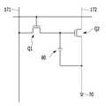
도 1은 본 발명의 한 실시예에 따른 박막 트랜지스터 기판의 배치도이다.
도 2는 도 1의 II-II선을 따라 잘라 도시한 단면도이다.
도 3 은 본 발명의 한 실시예에 따른 유기 발광 표시 장치의 한 화소를 나타낸 등가 회로도이다.
도 4는 도 3의 유기 발광 표시 장치의 한 화소의 배치도이다.
도 5는 도 4의 V-V선을 따라 잘라 도시한 단면도이다.
도 6은 도 4의 VI-VI선을 따라 잘라 도시한 단면도이다.1 is a layout diagram of a thin film transistor substrate according to an embodiment of the present invention.
2 is a cross-sectional view taken along the line II-II in FIG.
3 is an equivalent circuit diagram illustrating a pixel of an organic light emitting display according to an exemplary embodiment of the present invention.
4 is a layout diagram of one pixel of the OLED display of FIG.
5 is a cross-sectional view cut along the line VV in Fig.
6 is a cross-sectional view taken along the line VI-VI in Fig.
그러면 첨부한 도면을 참고로 하여 본 발명의 실시예에 대하여 본 발명이 속하는 기술 분야에서 통상의 지식을 가진 자가 용이하게 실시할 수 있도록 상세히 설명한다. 그러나 본 발명은 여러 가지 상이한 형태로 구현될 수 있으며 여기에서 설명하는 실시예에 한정되지 않는다.Hereinafter, embodiments of the present invention will be described in detail with reference to the accompanying drawings so that those skilled in the art can easily carry out the present invention. The present invention may, however, be embodied in many different forms and should not be construed as limited to the embodiments set forth herein.
도면에서 여러 층 및 영역을 명확하게 표현하기 위하여 두께를 확대하여 나타내었다. 명세서 전체를 통하여 유사한 부분에 대해서는 동일한 도면 부호를 붙였다. 층, 막, 영역, 판 등의 부분이 다른 부분 "위에" 있다고 할 때, 이는 다른 부분 "바로 위에" 있는 경우 뿐만 아니라 그 중간에 또 다른 부분이 있는 경우도 포함한다. 반대로 어떤 부분이 다른 부분 "바로 위에" 있다고 할 때에는 중간에 다른 부분이 없는 것을 뜻한다.In the drawings, the thickness is enlarged to clearly represent the layers and regions. Like parts are designated with like reference numerals throughout the specification. Whenever a portion of a layer, film, region, plate, or the like is referred to as being "on" another portion, it includes not only the case where it is "directly on" another portion, but also the case where there is another portion in between. Conversely, when a part is "directly over" another part, it means that there is no other part in the middle.
먼저, 도 1을 참조하여 본 발명의 한 실시예에 따른 박막 트랜지스터 기판에 대하여 설명한다.First, a thin film transistor substrate according to an embodiment of the present invention will be described with reference to FIG.
도 1은 본 발명의 한 실시예에 따른 박막 트랜지스터 기판의 배치도이고, 도 2는 도 1의 II-II선을 따라 잘라 도시한 단면도이다.FIG. 1 is a layout view of a thin film transistor substrate according to an embodiment of the present invention, and FIG. 2 is a cross-sectional view taken along a line II-II in FIG.
도 1에 도시한 바와 같이, 투명한 유리 또는 플라스틱 따위로 만들어진 절연 기판(100) 위에 복수의 게이트선(gate line)(121)이 형성되어 있다.As shown in FIG. 1, a plurality of
게이트선(121)은 게이트 신호를 전달하며 주로 가로 방향으로 뻗어 있다. 각 게이트선(121)은 게이트선(121)으로부터 돌출한 복수의 게이트 전극(124)과 다른 층 또는 외부 구동 회로와의 접속을 위하여 면적이 넓은 끝 부분(도시하지 않음)을 포함한다.The
게이트선(121)은 알루미늄(Al)이나 알루미늄 합금 등 알루미늄 계열 금속, 은(Ag)이나 은 합금 등 은계열 금속, 구리(Cu)나 구리 합금 등 구리 계열 금속, 몰리브덴(Mo)이나 몰리브덴 합금 등 몰리브덴 계열 금속, 크롬(Cr), 탄탈륨(Ta) 및 티타늄(Ti) 따위로 만들어질 수 있다. 그러나 게이트 전극(124)은 물리적 성질이 다른 적어도 두 개의 도전막을 포함하는 다중막 구조를 가질 수도 있다.The
게이트선(121) 위에는 게이트 절연막(140)이 형성되어 있다.A
게이트 절연막(140)은 산화 규소(SiOx), 질화 규소(SiNx), 또는 산질화 실리콘(SiON) 등의 절연 물질을 포함할 수 있다. 게이트 절연막(140)은 스퍼터링 방법 등을 사용하여 형성할 수 있다.The
게이트 절연막(140) 위에는 산화물 반도체로 이루어진 복수의 반도체(154)가 형성되어 있다.A plurality of
산화물 반도체는 금속 산화물 반도체로서, 아연(Zn), 인듐(In), 갈륨(Ga), 주석(Sn), 티타늄(Ti) 등의 금속의 산화물 또는 아연(Zn), 인듐(In), 갈륨(Ga), 주석(Sn), 티타늄(Ti) 등의 금속과 이들의 산화물의 조합으로 이루어질 수 있다. 예를 들어, 산화물 반도체는 산화 아연(ZnO), 아연-주석 산화물(ZTO), 아연-인듐 산화물(ZIO), 인듐 산화물(InO), 티타늄 산화물(TiO), 인듐-갈륨-아연 산화물(IGZO), 인듐-아연-주석 산화물(IZTO) 중 적어도 하나를 포함할 수 있다.Oxide semiconductors are metal oxide semiconductors. They are oxides of metals such as zinc (Zn), indium (In), gallium (Ga), tin (Sn), titanium (Ti), or oxides of zinc (Zn), indium Ga, tin (Sn), titanium (Ti), and oxides thereof. For example, the oxide semiconductors may be formed of at least one selected from the group consisting of zinc oxide (ZnO), zinc-tin oxide (ZTO), zinc-indium oxide (ZIO), indium oxide (InO), titanium oxide (TiO), indium- , And indium-zinc-tin oxide (IZTO).
반도체(154) 위에는 제1 층간 절연막(160)이 형성되어 있다. 제1 층간 절연막(160)은 질화 규소 또는 산화 규소로 단층 또는 복수층으로 형성될 수 있다.A first interlayer
제1 층간 절연막(160) 및 반도체(154) 위에는 복수의 데이터선(data line)(171)이 형성되어 있다.A plurality of
데이터선(171)은 데이터 신호를 전달하며 주로 세로 방향으로 뻗어 게이트선(121)과 교차한다. 각 데이터선(171)은 다른 층 또는 외부 구동 회로와의 접속을 위하여 면적이 넓은 끝 부분(도시하지 않음)을 포함한다.The
데이터선(171)은 저저항 금속인 구리, 티타늄, 몰리브덴, 알루미늄 따위로 단층 또는 복수층으로 이루어질 수 있다. 이때, 데이터선(171)은 5,000Å이상의 두께일 수 있다.The
데이터선(171) 위에는 제2 층간 절연막(180)이 형성되어 있다.On the
제2 층간 절연막(180)은 질화규소나 산화규소 따위의 무기 절연물, 유기 절연물, 저유전율 절연물 따위로 만들어진다. 유기 절연물 및 저유전율 절연물은 두껍게 형성되어 기판을 평탄하게 할 수 있다.The second
제1 층간 절연막(160) 및 제2 층간 절연막(180)에는 반도체(154)를 드러내는 복수의 접촉 구멍(contact hole)(183, 185)이 형성되어 있고, 제2 층간 절연막(180)에는 데이터선(171)을 드러내는 접촉 구멍(181)이 형성되어 있다.A plurality of
제2 층간 절연막(180) 위에는 소스 전극(173) 및 화소 전극(pixel electrode)(191)이 형성되어 있다.On the second
소스 전극(173)은 접촉 구멍(181, 183)을 통해서 데이터선(171)과 반도체(154)의 소스부를 연결한다.The
그리고 화소 전극(191)은 접촉 구멍(185)을 통해서 반도체(154)의 드레인부와 연결되며, 소스 전극(173)과 마주하는 부분을 포함한다. 소스 전극(173)과 마주하는 부분은 트랜지스터의 드레인 전극(175)이 된다.The
화소 전극(191) 및 소스 전극(173)은 ITO 및 IZO 중 적어도 하나를 포함하는 투명 도전 물질로 만들어질 수 있으며, 500Å이하의 두께로 형성될 수 있다.The
하나의 게이트 전극(124), 하나의 소스 전극(173) 및 하나의 드레인 전극은 반도체(154)와 함께 하나의 박막 트랜지스터(thin film transistor, TFT)를 이루며, 박막 트랜지스터의 채널은 소스 전극(173)과 드레인 전극 (175)사이의 반도체(154)에 형성된다.One
소스 전극(173) 및 드레인 전극(175)과 반도체(154)가 접촉하는 영역에는 오믹 접촉(ohmic contact)을 위해서 불순물이 도핑된 산화물 반도체가 위치할 수 있다.An oxide semiconductor doped with an impurity may be positioned in an area where the
본 발명의 한 실시예에서는 소스 전극(173) 및 드레인 전극(175)을 화소 전극(191)과 동일한 층에 동일한 물질로 형성함으로써, 드레인 전극과 화소 전극을 연결하기 위해서 접촉 구멍을 형성하는 공정을 생략할 수 있다.The
그리고 본 발명의 한 실시예에서는, 데이터선(171)은 저저항 금속으로 두껍게 형성하나, 소스 전극(173) 및 드레인 전극(175)은 화소 전극(191)과 같이 투명한 도전 물질로 데이터선(171)보다 얇게 형성하므로 습식 식각시 발생하는 스큐로 인한 언더컷 형성을 최소화할 수 있다. 즉, 습식 식각시 두께가 증가할수록 스큐로 인한 언더컷의 크기가 증가할 수 있으나, 본 발명의 실시예에서와 같이 소스 전극 및 드레인 전극을 데이터선보다 얇은 두께로 형성하면 스큐로 인한 언더컷의 크기를 최소화할 수 있다.The
따라서 언터컷으로 감소되는 폭만큼 크게 설계하지 않아도 되므로 소스 전극 및 드레인 전극의 크기를 줄일 수 있으므로, 트랜지스터의 크기가 작아지고 이로 인한 개구율 감소를 최소화할 수 있다.Therefore, the sizes of the source and drain electrodes can be reduced, so that the sizes of the transistors can be reduced and the decrease in the aperture ratio can be minimized.
또한, 본 발명의 한 실시예에서는 데이터선은 저저항 배선으로 형성하고, 트랜지스터의 소스 전극 및 드레인 전극은 투명한 도전 물질로 형성하므로 데이터선의 저항으로 인한 신호 지연이 발생하지 않는다.Also, in one embodiment of the present invention, the data line is formed of a low resistance wiring, and the source and drain electrodes of the transistor are formed of a transparent conductive material, so that no signal delay due to the resistance of the data line occurs.
이상의 박막 트랜지스터 기판은 액정 표시 장치의 하부 기판 및 유기 발광 표시 장치의 기판으로 사용될 수 있다.The thin film transistor substrate can be used as a lower substrate of a liquid crystal display device and a substrate of an organic light emitting display device.
이하에서는 도 1 및 도 2의 박막 트랜지스터 기판을 포함하는 유기 발광 표시 장치에 대해서 도 3 내지 도 6을 참조하여 구체적으로 설명한다.Hereinafter, an OLED display device including the thin film transistor substrate of FIGS. 1 and 2 will be described in detail with reference to FIGS. 3 to 6. FIG.
도 3 은 본 발명의 한 실시예에 따른 유기 발광 표시 장치의 한 화소를 나타낸 등가 회로도이다.3 is an equivalent circuit diagram illustrating a pixel of an organic light emitting display according to an exemplary embodiment of the present invention.
도 3에 도시한 바와 같이, 본 발명에 따른 하나의 화소(PE)는 유기 발광 소자(organic light emitting diode)(70), 두 개의 박막 트랜지스터(thin film transistor, TFT)(Q1, Q2), 그리고 하나의 축전기(capacitor)(80)를 구비하는 2Tr-1Cap 구조를 갖는다. 하지만, 본 발명의 한 실시예가 이에 한정되는 것은 아니다. 따라서 유기 발광 표시 장치(1000)는 하나의 화소(PE)에 셋 이상의 박막 트랜지스터와 둘 이상의 축전기를 구비할 수 있으며, 별도의 배선이 더 형성되어 다양한 구조를 갖도록 형성할 수도 있다. 이와 같이 추가로 형성되는 박막 트랜지스터 및 축전기는 보상 회로의 구성이 될 수 있다.As shown in FIG. 3, one pixel PE according to the present invention includes an organic
보상 회로는 각 화소(PE)마다 형성된 유기 발광 소자(70)의 균일성을 향상시켜 화질에 편차가 생기는 것을 억제한다. 일반적으로 보상 회로는 2개 내지 8개의 박막 트랜지스터를 포함한다.The compensation circuit improves the uniformity of the organic
유기 발광 소자(70)는 정공 주입 전극인 애노드(anode) 전극과 전자 주입 전극인 캐소드(cathode) 전극, 그리고 애노드 전극과 캐소드 전극 사이에 배치된 유기 발광층을 포함한다.The organic
본 발명의 한 실시예에서 하나의 화소(PE)는 제1 박막 트랜지스터(Q1)와 제2 박막 트랜지스터(Q2)를 포함한다.In one embodiment of the present invention, one pixel PE includes a first thin film transistor Q1 and a second thin film transistor Q2.
제1 박막 트랜지스터(Q1) 및 제2 박막 트랜지스터(Q2)는 각각 게이트 전극, 반도체, 소스 전극 및 드레인 전극을 포함한다. 그리고 제1 박막 트랜지스터(Q1) 및 제2 박막 트랜지스터(Q2) 중 하나 이상의 박막 트랜지스터의 반도체는 산화물 반도체로 이루어진다. 그리고 제1 박막 트랜지스터 및 제2 박막 트랜지스터 중 하나 이상의 소스 전극 및 드레인 전극은 투명한 도전성 물질인 ITO 및 IZO 중 적어도 하나를 포함할 수 있으며, 유기 발광 소자의 애노드 전극과 동일한 물질일 수 있다.The first thin film transistor Q1 and the second thin film transistor Q2 each include a gate electrode, a semiconductor, a source electrode, and a drain electrode. The semiconductor of at least one of the first thin film transistor Q1 and the second thin film transistor Q2 is made of an oxide semiconductor. At least one of the source electrode and the drain electrode of the first thin film transistor and the second thin film transistor may include at least one of ITO and IZO which are transparent conductive materials and may be the same material as the anode electrode of the organic light emitting device.
데이터선(171)에는 제1 박막 트랜지스터(Q1)의 소스 전극이 연결되고, 게이트선(121)에는 제1 박막 트랜지스터(Q1)의 게이트 전극이 연결된다. 그리고 제1 박막 트랜지스터(Q1)의 드레인 전극은 축전기(80)와 연결된다. 제1 박막 트랜지스터(Q1)의 드레인 전극과 축전기(80) 사이에 노드가 형성되어 제2 박막 트랜지스터(Q2)의 게이트 전극이 연결된다. 그리고 제2 박막 트랜지스터(Q2)의 소스 전극에는 공통 전원선(172)이 연결되며, 드레인 전극에는 유기 발광 소자(70)의 애노드 전극이 연결된다. A source electrode of the first thin film transistor Q1 is connected to the
제1 박막 트랜지스터(Q1)는 발광시키고자 하는 화소를 선택하는 스위칭 소자로 사용된다. 제1 박막 트랜지스터(Q1)가 순간적으로 턴온되며 축전기(80)는 충전되고, 이때 충전되는 전하량은 데이터선(171)으로부터 인가되는 전압의 전위에 비례한다. 그리고 제1 박막 트랜지스터(Q1)가 턴오프된 상태에서 축전기 선(도시하지 않음)에 한 프레임 주기로 전압이 증가하는 신호가 입력되면, 제2 박막 트랜지스터(Q2)의 게이트 전위는 축전기(80)에 충전된 전위를 기준으로 인가되는 전압의 레벨이 축전기 선을 통하여 인가되는 전압을 따라서 상승한다. 그리고 제2 박막 트랜지스터(Q2)는 게이트 전위가 문턱 전압을 넘으면 턴온된다. 그러면 공통 전원선(172)에 인가되던 전압이 제2 박막 트랜지스터(Q2)를 통하여 유기 발광 소자(70)에 인가되고, 유기 발광 소자(70)는 발광한다.The first thin film transistor Q1 is used as a switching element for selecting a pixel to emit light. The first thin film transistor Q1 is instantaneously turned on and the
이하, 도 4 내지 도 6을 참조하여, 본 발명의 한 실시예에 따른 유기 발광 표시 장치를 구체적으로 설명한다.Hereinafter, an organic light emitting display according to an embodiment of the present invention will be described in detail with reference to FIGS. 4 to 6. FIG.
도 4는 도 3의 유기 발광 표시 장치의 한 화소의 배치도이고, 도 5는 도 4의 V-V선을 따라 잘라 도시한 단면도이고, 도 6은 도 4의 VI-VI선을 따라 잘라 도시한 단면도이다.4 is a cross-sectional view taken along the line VV in FIG. 4, and FIG. 6 is a cross-sectional view taken along the line VI-VI in FIG. 4 .
도 4 내지 도 6을 참조하면, 기판(100) 위에는 게이트선(121), 제2 게이트 전극(128) 및 축전기용 제1 도전체(123)가 형성되어 있다.4 to 6, a
기판(100)은 유리, 석영, 세라믹 또는 플라스틱 등으로 이루어진 절연성 기판 일 수 있으며, 기판(100)은 스테인리스 강 등으로 이루어진 금속성 기판일 수 있다.The
게이트선(121)은 게이트선으로부터 돌출한 제1 게이트 전극(126)을 포함한다. 게이트선(121), 제2 게이트 전극(128) 및 축전기용 제1 도전체(123)은 알루미늄(Al)이나 알루미늄 합금 등 알루미늄 계열 금속, 은(Ag)이나 은 합금 등 은계열 금속, 구리(Cu)나 구리 합금 등 구리 계열 금속, 몰리브덴(Mo)이나 몰리브덴 합금 등 몰리브덴 계열 금속, 크롬(Cr), 탄탈륨(Ta) 및 티타늄(Ti) 따위로 만들어질 수 있다. 그러나 게이트선(121), 제2 게이트 전극(128) 및 축전기용 제1 도전체(123)은 물리적 성질이 다른 적어도 두 개의 도전막을 포함하는 다중막 구조를 가질 수도 있다.The
게이트선(121), 제2 게이트 전극(128) 및 축전기용 제1 도전체(123) 위에는 게이트 절연막(140)이 형성되어 있다.A
게이트 절연막(140)은 산화 규소(SiOx), 질화 규소(SiNx), 또는 산질화 실리콘(SiON) 등의 절연 물질을 포함할 수 있다. 게이트 절연막(140)은 스퍼터링 방법 등을 사용하여 형성할 수 있다.The
게이트 절연막(140) 위에는 산화물 반도체로 이루어진 복수의 제1 반도체(157) 및 제2 반도체(159)가 형성되어 있다.A plurality of
산화물 반도체는 금속 산화물 반도체로서, 아연(Zn), 인듐(In), 갈륨(Ga), 주석(Sn), 티타늄(Ti) 등의 금속의 산화물 또는 아연(Zn), 인듐(In), 갈륨(Ga), 주석(Sn), 티타늄(Ti) 등의 금속과 이들의 산화물의 조합으로 이루어질 수 있다. 예를 들어, 산화물 반도체는 산화 아연(ZnO), 아연-주석 산화물(ZTO), 아연-인듐 산화물(ZIO), 인듐 산화물(InO), 티타늄 산화물(TiO), 인듐-갈륨-아연 산화물(IGZO), 인듐-아연-주석 산화물(IZTO) 중 적어도 하나를 포함할 수 있다.Oxide semiconductors are metal oxide semiconductors. They are oxides of metals such as zinc (Zn), indium (In), gallium (Ga), tin (Sn), titanium (Ti), or oxides of zinc (Zn), indium Ga, tin (Sn), titanium (Ti), and oxides thereof. For example, the oxide semiconductors may be formed of at least one selected from the group consisting of zinc oxide (ZnO), zinc-tin oxide (ZTO), zinc-indium oxide (ZIO), indium oxide (InO), titanium oxide (TiO), indium- , And indium-zinc-tin oxide (IZTO).
반도체(157, 159) 위에는 제1 층간 절연막(160)이 형성되어 있다. 제1 층간 절연막(160)은 질화 규소 또는 산화 규소로 단층 또는 복수층으로 이루어질 수 있다.A first
제1 층간 절연막(160) 및 반도체(157, 159) 위에는 복수의 데이터선(171) 및 공통 전원선(172)이 형성되어 있다.A plurality of
데이터선(171)은 데이터 신호를 전달하며 게이트선(121)과 교차하는 방향으로 뻗어 있다.The
공통 전원선(172)은 일정 전압을 전달하며 데이터선(171)과 분리되어 같은 방향으로 뻗어 있다.The
데이터선(171) 및 공통 전원선(172)은 저저항 금속인 구리, 티타늄, 몰리브덴, 알루미늄 따위로 단층 또는 복수층으로 이루어질 수 있다. 데이터선(171) 및 공통 전원선(172)은 5,000Å이상의 두께로 형성되어 있다.The
데이터선(171) 및 공통 전원선(172) 위에는 제2 층간 절연막(180)이 형성되어 있다.A second
제2 층간 절연막(180)은 질화규소나 산화규소 따위의 무기 절연물, 유기 절연물, 저유전율 절연물 따위로 만들어진다. 유기 절연물 및 저유전율 절연물은 두껍게 형성되어 기판을 평탄하게 할 수 있다.The second
제1 층간 절연막(160) 및 제2 층간 절연막(180)에는 반도체(157, 159)를 노출하는 접촉 구멍(183, 185, 163, 165)이 형성되어 있고, 제2 층간 절연막(180)에는 데이터선(171), 공통 전원선(172) 및 축전기용 제2 도전체(95)를 드러내는 복수의 접촉 구멍(181, 167, 187)이 형성되어 있고, 제1 층간 절연막(160) 및 게이트 절연막(140)에는 제2 게이트 전극(128)을 노출하는 접촉 구멍(161)이 형성되어 있다.Contact holes 183, 185, 163 and 165 for exposing the
제2 층간 절연막(180) 위에는 제1 소스 전극(93), 제1 드레인 전극(95), 축전기용 제3 도전체(97), 제2 소스 전극(99), 제1 드레인 전극(91) 및 제1 전극(710)이 형성되어 있다.A
제1 소스 전극(93)은 접촉 구멍(181, 183)을 통해서 데이터선(171) 및 제1 반도체(157)의 소스부와 연결되어 데이터선(171)으로부터 전달되는 데이터 신호를 제1 드레인 전극(95)으로 전달한다.The
제1 드레인 전극(95)은 접촉 구멍(185, 187)을 통해서 제1 반도체(157)의 드레인부 및 축전기용 제2 도전체(75)와 연결되어 있고, 축전기용 제2 도전체(75)는 접촉 구멍(187, 161)을 통해서 제1 드레인 전극(95) 및 제2 게이트 전극(128)과 연결되어 있다.The
따라서, 제1 드레인 전극(95)으로 전달된 신호는 축전기용 제2 도전체(75)를 통해서 제2 게이트 전극(128)으로 전달된다.Accordingly, the signal transmitted to the
그리고 축전기용 제1 도전체(123)와 제3 도전체(97)는 접촉 구멍(189)을 통해서 전기적으로 연결된다. 따라서, 축전기용 제2 도전체(75)는 게이트 절연막(140) 및 제1 층간 절연막(160)을 유전체로 제1 도전체(123)와 하부 축전기를 이루고, 제2 층간 절연막(180)을 유전체로 제3 도전체(75)와 상부 축전기를 이룬다. 하부 축전기와 상부 축전기는 병렬 연결되어 축전기의 정전 용량을 증가시킨다.The
제2 소스 전극(99)은 접촉 구멍(167,163)을 통해서 공통 전원선(172) 및 제2 반도체(159)의 소스부와 연결되어 있으며, 공통 전원선으로부터 전달되는 신호를 제2 드레인 전극(91)으로 전달한다.The
제2 드레인 전극(91)은 접촉 구멍(165)을 통해서 제2 반도체(159)의 드레인부와 연결된다. 제2 드레인 전극(91)은 제1 전극(710)과 일체형으로 형성될 수 있으며, 제2 드레인 전극(91)으로부터 전달되는 신호를 제1 전극(710)에 전달한다. 제1 전극(710)은 유기 발광 소자(70)의 애노드 전극이 된다.The
제1 소스 전극(93), 제1 드레인 전극(95), 축전기용 제3 도전체(97), 제2 소스 전극(99), 제2 드레인 전극(91) 및 제1 전극(710)은 ITO 및 IZO 를 적어도 하나 포함하는 투명 도전 물질로 만들어질 수 있으며, 500Å이하의 두께로 형성될 수 있다.The
유기 발광 소자(70)의 제1 전극(710) 위에는 화소 정의막(810)이 형성되어 있다.A
화소 정의막(810)은 제1 전극(710)을 노출하는 개구부(195)를 가진다. 화소 정의막(810)은 폴리아크릴계(polyacrylates) 또는 폴리이미드계(polyimides) 등의 수지와 실리카 계열의 무기물 등을 포함하여 이루어질 수 있다.The
화소 정의막(810)의 개구부(195)에는 유기 발광층(720)이 형성되어 있다.An
유기 발광층(720)은 발광층, 정공 수송층(hole-injection layer, HIL), 정공 수송층(hole-transporting layer, HTL), 전자 수송층(electron-transporting layer, ETL) 및 전자 주입층(electron-injection layer, EIL) 중 하나 이상을 포함하는 복수층으로 형성된다.The organic
유기 발광층(720)이 이들 모두를 포함할 경우 정공 주입층이 애노드 전극인 제1 전극(710) 위에 위치하고 그 위로 정공 수송층, 발광층, 전자 수송층, 전자 주입층이 차례로 적층될 수 있다.When the organic
화소 정의막(810) 및 유기 발광층(720) 위에는 제2 전극(730)이 형성된다.A
제2 전극(730)은 유기 발광 소자의 캐소드 전극이 된다. 따라서 제1 전극(710), 유기 발광층(720) 및 제2 전극(730)은 유기 발광 소자(70)를 이룬다.The
제2 전극(730)은 반사막, 투명막 또는 반투과막으로 형성한다.The
반사막 및 반투과막은 마그네슘(Mg), 은(Ag), 금(Au), 칼슘(Ca), 리튬(Li), 크롬(Cr) 및 알루미늄(Al) 중 하나 이상의 금속 또는 이들의 합금을 사용하여 만들어진다. 반사막과 반투과막은 두께로 결정되며, 반투과막은 200nm 이하의 두께로 형성될 수 있다. 두께가 얇아질수록 빛의 투과율이 높아지나, 너무 얇으면 저항이 증가한다.The reflective film and the semi-transparent film may be formed using at least one of magnesium (Mg), silver (Ag), gold (Au), calcium (Ca), lithium (Li), chromium (Cr) Is made. The reflective film and the semi-transmissive film are determined to have a thickness, and the semi-transmissive film can be formed to a thickness of 200 nm or less. The thinner the thickness, the higher the transmittance of light, but if it is too thin, the resistance increases.
투명막은 ITO(indium tin oxide), IZO(indium zinc oxide), ZnO(산화 아연) 등의 물질로 이루어진다.The transparent film is made of a material such as indium tin oxide (ITO), indium zinc oxide (IZO), or zinc oxide (ZnO).
이상에서 본 발명의 바람직한 실시예에 대하여 상세하게 설명하였지만 본 발명의 권리범위는 이에 한정되는 것은 아니고 다음의 청구범위에서 정의하고 있는 본 발명의 기본 개념을 이용한 당업자의 여러 변형 및 개량 형태 또한 본 발명의 권리범위에 속하는 것이다.While the present invention has been particularly shown and described with reference to exemplary embodiments thereof, it is to be understood that the invention is not limited to the disclosed exemplary embodiments, Of the right.
Claims (15)
Translated fromKorean상기 기판 위에 위치하는 제1 신호선,
상기 제1 신호선과 교차하는 제2 신호선 및 제3 신호선,
상기 제1 신호선 및 제2 신호선과 연결되어 있는 제1 트랜지스터,
상기 제1 트랜지스터 및 상기 제3 신호선과 연결되어 있는 제2 트랜지스터,
상기 제2 트랜지스터와 연결되어 있는 유기 발광 소자
를 포함하고,
상기 제1 트랜지스터 및 제2 트랜지스터의 소스 전극 및 드레인 전극과 상기 제2 트랜지스터와 연결되어 있는 상기 유기 발광 소자의 제1 전극은 동일한 층에 동일한 물질로 형성되어 있고,
상기 기판 위에 위치하는 축전기용 제1 도전체,
상기 축전기용 제1 도전체 위에 위치하는 게이트 절연막,
상기 게이트 절연막 위에 위치하는 제1 층간 절연막,
상기 제1 층간 절연막 위에 위치하는 축전기용 제2 도전체,
상기 축전기용 제2 도전체 위에 위치하는 제2 층간 절연막,
상기 제2 층간 절연막 위에 위치하는 축전기용 제3 도전체
로 이루어지는 축전기를 더 포함하고,
상기 제1 도전체는 상기 제1 신호선과 동일한 물질로 이루어지고,
상기 제2 도전체는 상기 제2 신호선 및 제3 신호선과 동일한 물질로 이루어지고,
상기 제3 도전체는 상기 제1 전극과 동일한 물질로 이루어지는 유기 발광 표시 장치.Board,
A first signal line located on the substrate,
A second signal line and a third signal line crossing the first signal line,
A first transistor connected to the first signal line and the second signal line,
A second transistor connected to the first transistor and the third signal line,
And the organic light emitting diode
Lt; / RTI >
Wherein a source electrode and a drain electrode of the first transistor and the second transistor and a first electrode of the organic light emitting element connected to the second transistor are formed of the same material in the same layer,
A first conductor for a capacitor located on the substrate,
A gate insulating film located on the first conductor for the capacitor,
A first interlayer insulating film located above the gate insulating film,
A second conductor for a capacitor located on the first interlayer insulating film,
A second interlayer insulating film located on the second conductor for the capacitor,
A third capacitor for a capacitor located on the second interlayer insulating film
Further comprising a capacitor,
Wherein the first conductor is made of the same material as the first signal line,
The second conductor is made of the same material as the second signal line and the third signal line,
And the third conductive material is made of the same material as the first electrode.
상기 제1 트랜지스터 및 제2 트랜지스터 중 적어도 하나의 소스 전극 및 드레인 전극과 상기 제2 트랜지스터와 연결되어 있는 상기 유기 발광 소자의 제1 전극은 투명한 도전 물질로 이루어지는 유기 발광 표시 장치.The method of claim 6,
Wherein a source electrode and a drain electrode of at least one of the first transistor and the second transistor and a first electrode of the organic light emitting element connected to the second transistor are made of a transparent conductive material.
상기 제1 트랜지스터 및 제2 트랜지스터의 소스 전극 및 드레인 전극은 상기 제2 신호선 및 제3 신호선보다 얇은 두께로 형성되어 있는 유기 발광 표시 장치.8. The method of claim 7,
And a source electrode and a drain electrode of the first transistor and the second transistor are formed to be thinner than the second signal line and the third signal line.
상기 투명한 도전 물질은 ITO 및 IZO 중 적어도 하나를 포함하는 유기 발광 표시 장치.9. The method of claim 8,
Wherein the transparent conductive material comprises at least one of ITO and IZO.
상기 제2 신호선 및 제3 신호선 위에 위치하는 층간 절연막을 더 포함하고,
상기 제1 트랜지스터 및 제2 트랜지스터 중 적어도 하나의 소스 전극 및 드레인 전극과 상기 제2 트랜지스터와 연결되어 있는 상기 유기 발광 소자의 제1 전극은 상기 층간 절연막 위에 위치하는 유기 발광 표시 장치.8. The method of claim 7,
Further comprising an interlayer insulating film located over the second signal line and the third signal line,
Wherein a source electrode and a drain electrode of at least one of the first transistor and the second transistor and a first electrode of the organic light emitting element connected to the second transistor are located on the interlayer insulating film.
상기 제1 트랜지스터의 소스 전극은 상기 층간 절연막의 제1 접촉 구멍을 통해서 상기 제2 신호선과 연결되고,
상기 제2 트랜지스터의 소스 전극은 상기 층간 절연막의 제2 접촉 구멍을 통해서 상기 제3 신호선과 연결되는 유기 발광 표시 장치.11. The method of claim 10,
A source electrode of the first transistor is connected to the second signal line through a first contact hole of the interlayer insulating film,
And a source electrode of the second transistor is connected to the third signal line through a second contact hole of the interlayer insulating film.
상기 제2 신호선은 데이터 신호가 인가되는 데이터선이고,
상기 제3 신호선은 정전압이 인가되는 공통 전원선인 유기 발광 표시 장치.12. The method of claim 11,
The second signal line is a data line to which a data signal is applied,
And the third signal line is a common power line to which a constant voltage is applied.
상기 제1 도전체는 상기 게이트 절연막, 상기 제1 층간 절연막 및 상기 제2 층간 절연막에 형성된 제3 접촉 구멍을 통해서 상기 제3 도전체와 전기적으로 연결되는 유기 발광 표시 장치.The method of claim 6,
Wherein the first conductor is electrically connected to the third conductor through a third contact hole formed in the gate insulating film, the first interlayer insulating film, and the second interlayer insulating film.
Priority Applications (4)
| Application Number | Priority Date | Filing Date | Title |
|---|---|---|---|
| KR1020120115358AKR101942489B1 (en) | 2012-10-17 | 2012-10-17 | Thin film transistor array panel and organic light emitting diode display including the same |
| CN201310365525.0ACN103779355B (en) | 2012-10-17 | 2013-08-21 | Thin film transistor base plate and organic light-emitting display device comprising this |
| TW102130381ATW201417268A (en) | 2012-10-17 | 2013-08-26 | Thin film transistor array panel and organic light emitting diode display therewith |
| US14/055,253US9391212B2 (en) | 2012-10-17 | 2013-10-16 | Thin film transistor array panel and organic light emitting diode display including the same |
Applications Claiming Priority (1)
| Application Number | Priority Date | Filing Date | Title |
|---|---|---|---|
| KR1020120115358AKR101942489B1 (en) | 2012-10-17 | 2012-10-17 | Thin film transistor array panel and organic light emitting diode display including the same |
Publications (2)
| Publication Number | Publication Date |
|---|---|
| KR20140049285A KR20140049285A (en) | 2014-04-25 |
| KR101942489B1true KR101942489B1 (en) | 2019-01-28 |
Family
ID=50474578
Family Applications (1)
| Application Number | Title | Priority Date | Filing Date |
|---|---|---|---|
| KR1020120115358AActiveKR101942489B1 (en) | 2012-10-17 | 2012-10-17 | Thin film transistor array panel and organic light emitting diode display including the same |
Country Status (4)
| Country | Link |
|---|---|
| US (1) | US9391212B2 (en) |
| KR (1) | KR101942489B1 (en) |
| CN (1) | CN103779355B (en) |
| TW (1) | TW201417268A (en) |
Families Citing this family (16)
| Publication number | Priority date | Publication date | Assignee | Title |
|---|---|---|---|---|
| US20150316804A1 (en)* | 2012-12-28 | 2015-11-05 | Sharp Kabushiki Kaisha | Conductive structure, method for producing conductive structure, and display device |
| KR102049443B1 (en)* | 2013-05-15 | 2019-11-28 | 삼성디스플레이 주식회사 | Organic light emitting display device and method of manufacturing thereof |
| KR102097023B1 (en)* | 2013-06-17 | 2020-04-06 | 삼성디스플레이 주식회사 | Display device and method for manufacturing display device |
| KR101640192B1 (en) | 2014-08-05 | 2016-07-18 | 삼성디스플레이 주식회사 | Display apparatus |
| CN104362127A (en)* | 2014-11-21 | 2015-02-18 | 深圳市华星光电技术有限公司 | Manufacturing method and device for thin film transistor substrate |
| KR102297760B1 (en)* | 2014-12-31 | 2021-09-03 | 엘지디스플레이 주식회사 | Liquid crystal display device with oxide thin film transistor |
| KR102403194B1 (en) | 2015-06-26 | 2022-05-27 | 삼성디스플레이 주식회사 | Display apparatus |
| KR102620018B1 (en)* | 2016-09-30 | 2024-01-02 | 삼성디스플레이 주식회사 | Organic light emitting display device and test method of open short thereof |
| CN106876415B (en)* | 2017-03-20 | 2019-09-10 | 上海天马微电子有限公司 | Thin film transistor array substrate and manufacturing method thereof |
| KR102569929B1 (en)* | 2018-07-02 | 2023-08-24 | 삼성디스플레이 주식회사 | Display apparatus |
| CN109148480B (en)* | 2018-08-21 | 2021-03-16 | 武汉华星光电半导体显示技术有限公司 | Array substrate |
| KR102722115B1 (en) | 2019-12-31 | 2024-10-28 | 엘지디스플레이 주식회사 | Organic light emitting diode display device and method of manufacturing the same |
| KR20210088045A (en)* | 2020-01-03 | 2021-07-14 | 삼성디스플레이 주식회사 | Display device |
| KR20210104213A (en)* | 2020-02-14 | 2021-08-25 | 삼성디스플레이 주식회사 | Display device and method for manufacturing the same |
| WO2021240584A1 (en)* | 2020-05-25 | 2021-12-02 | シャープ株式会社 | Display device and production method for display device |
| KR20220016373A (en)* | 2020-07-30 | 2022-02-09 | 삼성디스플레이 주식회사 | Display apparatus and manufacturing the same |
Citations (1)
| Publication number | Priority date | Publication date | Assignee | Title |
|---|---|---|---|---|
| KR100739649B1 (en)* | 2006-10-16 | 2007-07-13 | 삼성에스디아이 주식회사 | Organic electroluminescent display and manufacturing method thereof |
Family Cites Families (12)
| Publication number | Priority date | Publication date | Assignee | Title |
|---|---|---|---|---|
| JP3391343B2 (en)* | 1999-10-26 | 2003-03-31 | 日本電気株式会社 | Active matrix substrate and manufacturing method thereof |
| KR100699995B1 (en)* | 2004-09-02 | 2007-03-26 | 삼성에스디아이 주식회사 | Organic electroluminescent device and manufacturing method thereof |
| KR100953596B1 (en) | 2004-11-10 | 2010-04-21 | 캐논 가부시끼가이샤 | Light emitting device |
| US7576354B2 (en)* | 2005-12-20 | 2009-08-18 | Samsung Mobile Display Co., Ltd. | Organic light emitting diode display and method of fabricating the same |
| JP2008257086A (en)* | 2007-04-09 | 2008-10-23 | Sony Corp | Display device, display device manufacturing method, and electronic apparatus |
| KR100922063B1 (en) | 2008-02-04 | 2009-10-16 | 삼성모바일디스플레이주식회사 | Organic electroluminescent display |
| KR20090105561A (en) | 2008-04-03 | 2009-10-07 | 삼성모바일디스플레이주식회사 | Semiconductor device and flat panel display device having same |
| KR101533391B1 (en)* | 2008-08-06 | 2015-07-02 | 삼성디스플레이 주식회사 | Thin film transistor substrate and manufacturing method thereof |
| EP2172804B1 (en)* | 2008-10-03 | 2016-05-11 | Semiconductor Energy Laboratory Co, Ltd. | Display device |
| JP4844617B2 (en)* | 2008-11-05 | 2011-12-28 | ソニー株式会社 | Thin film transistor substrate and display device |
| KR101015850B1 (en) | 2009-02-09 | 2011-02-24 | 삼성모바일디스플레이주식회사 | Organic light emitting display device manufacturing method |
| JP2010206154A (en)* | 2009-02-09 | 2010-09-16 | Hitachi Displays Ltd | Display device |
- 2012
- 2012-10-17KRKR1020120115358Apatent/KR101942489B1/enactiveActive
- 2013
- 2013-08-21CNCN201310365525.0Apatent/CN103779355B/enactiveActive
- 2013-08-26TWTW102130381Apatent/TW201417268A/enunknown
- 2013-10-16USUS14/055,253patent/US9391212B2/enactiveActive
Patent Citations (1)
| Publication number | Priority date | Publication date | Assignee | Title |
|---|---|---|---|---|
| KR100739649B1 (en)* | 2006-10-16 | 2007-07-13 | 삼성에스디아이 주식회사 | Organic electroluminescent display and manufacturing method thereof |
Also Published As
| Publication number | Publication date |
|---|---|
| US9391212B2 (en) | 2016-07-12 |
| US20140103317A1 (en) | 2014-04-17 |
| CN103779355B (en) | 2019-01-11 |
| CN103779355A (en) | 2014-05-07 |
| TW201417268A (en) | 2014-05-01 |
| KR20140049285A (en) | 2014-04-25 |
Similar Documents
| Publication | Publication Date | Title |
|---|---|---|
| KR101942489B1 (en) | Thin film transistor array panel and organic light emitting diode display including the same | |
| KR102699702B1 (en) | Array Substrate For Thin Film Transistor | |
| KR101073542B1 (en) | Organic light emitting diode display and method for manufacturing the same | |
| US10644165B2 (en) | Thin-film transistor, method of fabricating thin-film transistor, and display device | |
| US9768310B2 (en) | Thin film transistor, organic light-emitting diode display including the same, and manufacturing method thereof | |
| CN108172595B (en) | Thin Film Transistor Substrate | |
| CN102097486B (en) | Thin film transistor, method of manufacturing the same, and organic electroluminescent device | |
| KR101147414B1 (en) | Organic light emitting diode display and method for manufacturing the same | |
| EP2009695A2 (en) | Thin film transistor method of fabricating the same organic light emitting diode display device including the same and method of fabricating the same | |
| US10204973B2 (en) | Display device and thin-film transistors substrate | |
| KR102530003B1 (en) | Transistor array panel and display device including the same | |
| US11374027B2 (en) | Manufacturing method of thin film transistor substrate and thin film transistor substrate | |
| US9893193B2 (en) | Thin-film transistor including a gate electrode with a side wall insulating layer and display device | |
| KR20150011219A (en) | Thin film transistor and thin film transistor array panel including the same | |
| US9177971B2 (en) | Thin film transistor array panel and method for manufacturing the same | |
| KR20180021958A (en) | Thin film transistor, manufacturing method thereof, and display device including thereof | |
| CN113658958B (en) | Display panel and preparation method thereof | |
| JP6209918B2 (en) | THIN FILM TRANSISTOR AND METHOD FOR MANUFACTURING THIN FILM TRANSISTOR | |
| KR20160049172A (en) | Thin film transistor array substrate and display device comprising the same | |
| JP6264015B2 (en) | THIN FILM TRANSISTOR AND METHOD FOR PRODUCING THIN FILM TRANSISTOR | |
| KR20150098699A (en) | Thin film transistor and display substrate comprising the thin film transistor | |
| KR20080052919A (en) | Method of manufacturing thin film transistor array panel and thin film transistor array panel |
Legal Events
| Date | Code | Title | Description |
|---|---|---|---|
| PA0109 | Patent application | Patent event code:PA01091R01D Comment text:Patent Application Patent event date:20121017 | |
| PG1501 | Laying open of application | ||
| PA0201 | Request for examination | Patent event code:PA02012R01D Patent event date:20171013 Comment text:Request for Examination of Application Patent event code:PA02011R01I Patent event date:20121017 Comment text:Patent Application | |
| E902 | Notification of reason for refusal | ||
| PE0902 | Notice of grounds for rejection | Comment text:Notification of reason for refusal Patent event date:20180625 Patent event code:PE09021S01D | |
| E701 | Decision to grant or registration of patent right | ||
| PE0701 | Decision of registration | Patent event code:PE07011S01D Comment text:Decision to Grant Registration Patent event date:20181022 | |
| GRNT | Written decision to grant | ||
| PR0701 | Registration of establishment | Comment text:Registration of Establishment Patent event date:20190121 Patent event code:PR07011E01D | |
| PR1002 | Payment of registration fee | Payment date:20190121 End annual number:3 Start annual number:1 | |
| PG1601 | Publication of registration | ||
| PR1001 | Payment of annual fee | Payment date:20211228 Start annual number:4 End annual number:4 | |
| PR1001 | Payment of annual fee | Payment date:20221226 Start annual number:5 End annual number:5 |