KR101932576B1 - Semiconductor device and method for manufacturing the same - Google Patents
Semiconductor device and method for manufacturing the sameDownload PDFInfo
- Publication number
- KR101932576B1 KR101932576B1KR1020110088976AKR20110088976AKR101932576B1KR 101932576 B1KR101932576 B1KR 101932576B1KR 1020110088976 AKR1020110088976 AKR 1020110088976AKR 20110088976 AKR20110088976 AKR 20110088976AKR 101932576 B1KR101932576 B1KR 101932576B1
- Authority
- KR
- South Korea
- Prior art keywords
- film
- layer
- oxide semiconductor
- insulating layer
- oxide
- Prior art date
- Legal status (The legal status is an assumption and is not a legal conclusion. Google has not performed a legal analysis and makes no representation as to the accuracy of the status listed.)
- Expired - Fee Related
Links
Images


Classifications
- H—ELECTRICITY
- H01—ELECTRIC ELEMENTS
- H01L—SEMICONDUCTOR DEVICES NOT COVERED BY CLASS H10
- H01L21/00—Processes or apparatus adapted for the manufacture or treatment of semiconductor or solid state devices or of parts thereof
- H01L21/02—Manufacture or treatment of semiconductor devices or of parts thereof
- H01L21/02104—Forming layers
- H01L21/02365—Forming inorganic semiconducting materials on a substrate
- H01L21/02436—Intermediate layers between substrates and deposited layers
- H01L21/02439—Materials
- H01L21/02488—Insulating materials
- H—ELECTRICITY
- H01—ELECTRIC ELEMENTS
- H01L—SEMICONDUCTOR DEVICES NOT COVERED BY CLASS H10
- H01L21/00—Processes or apparatus adapted for the manufacture or treatment of semiconductor or solid state devices or of parts thereof
- H01L21/02—Manufacture or treatment of semiconductor devices or of parts thereof
- H01L21/02104—Forming layers
- H01L21/02365—Forming inorganic semiconducting materials on a substrate
- H01L21/02518—Deposited layers
- H01L21/02521—Materials
- H01L21/02551—Group 12/16 materials
- H01L21/02554—Oxides
- H—ELECTRICITY
- H01—ELECTRIC ELEMENTS
- H01L—SEMICONDUCTOR DEVICES NOT COVERED BY CLASS H10
- H01L21/00—Processes or apparatus adapted for the manufacture or treatment of semiconductor or solid state devices or of parts thereof
- H01L21/02—Manufacture or treatment of semiconductor devices or of parts thereof
- H01L21/02104—Forming layers
- H01L21/02365—Forming inorganic semiconducting materials on a substrate
- H01L21/02518—Deposited layers
- H01L21/02521—Materials
- H01L21/02565—Oxide semiconducting materials not being Group 12/16 materials, e.g. ternary compounds
- H—ELECTRICITY
- H10—SEMICONDUCTOR DEVICES; ELECTRIC SOLID-STATE DEVICES NOT OTHERWISE PROVIDED FOR
- H10D—INORGANIC ELECTRIC SEMICONDUCTOR DEVICES
- H10D30/00—Field-effect transistors [FET]
- H10D30/60—Insulated-gate field-effect transistors [IGFET]
- H10D30/67—Thin-film transistors [TFT]
- H10D30/674—Thin-film transistors [TFT] characterised by the active materials
- H10D30/6755—Oxide semiconductors, e.g. zinc oxide, copper aluminium oxide or cadmium stannate
- H—ELECTRICITY
- H10—SEMICONDUCTOR DEVICES; ELECTRIC SOLID-STATE DEVICES NOT OTHERWISE PROVIDED FOR
- H10D—INORGANIC ELECTRIC SEMICONDUCTOR DEVICES
- H10D30/00—Field-effect transistors [FET]
- H10D30/60—Insulated-gate field-effect transistors [IGFET]
- H10D30/67—Thin-film transistors [TFT]
- H10D30/6757—Thin-film transistors [TFT] characterised by the structure of the channel, e.g. transverse or longitudinal shape or doping profile
- H—ELECTRICITY
- H10—SEMICONDUCTOR DEVICES; ELECTRIC SOLID-STATE DEVICES NOT OTHERWISE PROVIDED FOR
- H10D—INORGANIC ELECTRIC SEMICONDUCTOR DEVICES
- H10D30/00—Field-effect transistors [FET]
- H10D30/60—Insulated-gate field-effect transistors [IGFET]
- H10D30/67—Thin-film transistors [TFT]
- H10D30/6758—Thin-film transistors [TFT] characterised by the insulating substrates
- H—ELECTRICITY
- H10—SEMICONDUCTOR DEVICES; ELECTRIC SOLID-STATE DEVICES NOT OTHERWISE PROVIDED FOR
- H10D—INORGANIC ELECTRIC SEMICONDUCTOR DEVICES
- H10D62/00—Semiconductor bodies, or regions thereof, of devices having potential barriers
- H10D62/40—Crystalline structures
- H—ELECTRICITY
- H10—SEMICONDUCTOR DEVICES; ELECTRIC SOLID-STATE DEVICES NOT OTHERWISE PROVIDED FOR
- H10D—INORGANIC ELECTRIC SEMICONDUCTOR DEVICES
- H10D62/00—Semiconductor bodies, or regions thereof, of devices having potential barriers
- H10D62/80—Semiconductor bodies, or regions thereof, of devices having potential barriers characterised by the materials
Landscapes
- Engineering & Computer Science (AREA)
- Physics & Mathematics (AREA)
- Condensed Matter Physics & Semiconductors (AREA)
- General Physics & Mathematics (AREA)
- Manufacturing & Machinery (AREA)
- Computer Hardware Design (AREA)
- Microelectronics & Electronic Packaging (AREA)
- Power Engineering (AREA)
- Thin Film Transistor (AREA)
- Liquid Crystal (AREA)
- Electroluminescent Light Sources (AREA)
- Recrystallisation Techniques (AREA)
- Chemical & Material Sciences (AREA)
- Crystallography & Structural Chemistry (AREA)
- Physical Deposition Of Substances That Are Components Of Semiconductor Devices (AREA)
- Formation Of Insulating Films (AREA)
Abstract
Translated fromKoreanDescription
Translated fromKorean본 발명은 산화물 반도체를 이용하는 반도체 장치 및 그 제작 방법에 관한 것이다.The present invention relates to a semiconductor device using an oxide semiconductor and a manufacturing method thereof.
또한, 본 명세서에서 반도체 장치란, 반도체 특성을 이용함으로써 기능할 수 있는 장치 전반을 나타내고, 전기 광학 장치, 반도체 회로 및 전자 기기는 모두 반도체 장치이다.
In the present specification, the semiconductor device refers to the entire device capable of functioning by using semiconductor characteristics, and the electro-optical device, the semiconductor circuit, and the electronic device are both semiconductor devices.
최근 절연 표면을 갖는 기판 상에 형성된 반도체 박막(두께 수십~수백nm 정도)을 이용하여 박막 트랜지스터(TFT)를 구성하는 기술이 주목을 받고 있다. 박막 트랜지스터는 IC나 전기 광학 장치와 같은 전자 디바이스에 널리 응용되고, 특히 화상표시 장치의 스위칭 소자로서 시급히 개발되고 있다. 금속 산화물은 다양하게 존재하여 다양한 용도로 이용되고 있다.BACKGROUND ART [0002] Recently, a technique of forming a thin film transistor (TFT) by using a semiconductor thin film (having a thickness of several tens to several hundreds of nm) formed on a substrate having an insulating surface has attracted attention. BACKGROUND ART Thin film transistors are widely used in electronic devices such as ICs and electro-optical devices, and are being developed particularly as switching devices for image display devices. Metal oxides exist in various forms and are used for various purposes.
금속 산화물 중에는 반도체 특성을 나타내는 것이 있다. 반도체 특성을 나타내는 금속 산화물로서는, 예를 들어 산화 텅스텐, 산화주석, 산화인듐, 산화아연 등이 있으며, 이와 같은 반도체 특성을 나타내는 금속 산화물을 채널 형성 영역에 이용하는 박막 트랜지스터가 이미 알려져 있다(일본국 특개2007-123861호 공보 및 특개2007-96055호 공보).Some metal oxides exhibit semiconductor properties. As a metal oxide showing semiconductor characteristics, for example, there are tungsten oxide, tin oxide, indium oxide, zinc oxide and the like, and a thin film transistor using a metal oxide showing such a semiconductor characteristic in a channel forming region is already known 2007-123861 and 2007-96055).
이와 같은 트랜지스터에 이용하는 산화물 반도체에 대해서 "산화물 반도체는 불순물에 대해서 둔감하며, 막 속에는 상당히 많은 금속 불순물이 포함되어 있어도 문제가 없으며, 나트륨과 같은 알칼리 금속이 다량으로 포함되는 저렴한 소다 석회 유리도 사용할 수 있다."라고 언급되어 있다("비정질 산화물 반도체의 물성과 디바이스 개발의 현상" 참조).
As for oxide semiconductors used in such transistors, "oxide semiconductors are insensitive to impurities, and even if the film contains a considerable amount of metal impurities, there is no problem, and a cheap soda lime glass containing a large amount of alkali metal such as sodium can be used Quot; (see " Physical Properties of Amorphous Oxide Semiconductor and the Development of Devices ").
산화물 반도체는 디바이스 제작 공정에서 전자 공여체를 형성하는 수소나 물의 혼입 등이 발생하면, 그 전기 전도도가 변화될 우려가 있다. 이와 같은 현상은 산화물 반도체를 이용한 트랜지스터에 있어서 전기적 특성의 변동 요인이 된다.When the oxide semiconductor is mixed with hydrogen or water to form an electron donor in the device fabrication process, the electric conductivity of the oxide semiconductor may change. Such a phenomenon is a factor of variation of electrical characteristics in a transistor using an oxide semiconductor.
또한, 산화물 반도체를 이용한 반도체 장치는 가시광이나 자외광을 조사함으로써 전기적 특성이 변화될 우려가 있다.Further, in a semiconductor device using an oxide semiconductor, electrical characteristics may be changed by irradiating visible light or ultraviolet light.
이와 같은 문제를 감안하여, 산화물 반도체막을 이용한 반도체 장치에 안정된 전기적 특성을 부여하고, 신뢰성이 높은 반도체 장치를 제작하는 것을 하나의 과제로 한다.In view of such a problem, it is a problem to manufacture a semiconductor device with high reliability by giving a stable electric characteristic to the semiconductor device using the oxide semiconductor film.
또한, 모유리와 같은 큰 기판을 이용하여 신뢰성이 높은 반도체 장치의 대량생산을 행할 수 있는 반도체 장치의 제작 프로세스를 제공하는 것을 하나의 과제로 한다.
Another object of the present invention is to provide a manufacturing process of a semiconductor device capable of mass production of a highly reliable semiconductor device by using a large substrate such as a mother glass.
개시하는 발명의 일 양태는 절연 표면 상에 제 1 재료막(육방정 결정 구조를 갖는 막)을 형성하고, 제 1 재료막을 핵으로 하여 육방정 결정 구조를 갖는 제 2 재료막(결정성 산화물 반도체막)을 형성하고, 제 1 재료막과 제 2 재료막의 적층을 형성하는 반도체 장치의 제작 방법이다. 또한, 제 1 재료막과 제 2 재료막은 다른 재료로 형성된다.In one aspect of the disclosed invention, a first material film (film having a hexagonal crystal structure) is formed on an insulating surface, and a second material film having a hexagonal crystal structure (a crystalline oxide semiconductor Film) is formed, and a lamination of the first material film and the second material film is formed. Further, the first material film and the second material film are formed of different materials.
구체적으로, 제 1 재료막은 섬유아연석형 결정 구조를 갖는 재료막(예를 들어, 질화 갈륨 또는 질화 알루미늄), 또는 코런덤형 결정 구조를 갖는 재료막(α-Al2O3, α-Ga2O3, In2O3, Ti2O3, V2O3, Cr2O3, 또는 α-Fe2O3)을 이용할 수 있다. 또한, 양호한 결정 구조를 얻기 위해서 이들 재료막을 적층시켜서 이용해도 되며, 예를 들어 질화 알루미늄막 상에 질화 갈륨막을 적층시킨 것을 이용해도 된다.Specifically, the first material a material having a film fiber zinc seokhyeong crystal structure film (for example, gallium nitride or aluminum nitride) material film having, or koreon deomhyeong crystal structure(α-Al 2 O 3, α-Ga 2 O3 , In2 O3 , Ti2 O3 , V2 O3 , Cr2 O3 , or α-Fe2 O3 ). In order to obtain a good crystal structure, these material films may be laminated or used. For example, a laminate of a gallium nitride film on an aluminum nitride film may be used.
또한, 섬유아연석형 결정 구조는 음이온과 양이온이 1:1로 결합하여 이루어질 수 있는 이온 결정에 보여지는 결정 구조의 하나이다. 도 6(A) 및 도 6(B)는 섬유아연석형 결정 구조를 도시한 도면이며, 검은색 동그라미가 갈륨 또는 알루미늄, 하얀색 동그라미가 산소를 나타낸다. 도 6(A)는 a-b면에서의 섬유아연석형 결정 구조의 모식도이며, 도 6(B)는 c축방향을 세로방향으로 한 섬유아연석형 결정 구조의 모식도이다.In addition, the fiber-zinc-zoned crystal structure is one of the crystal structures shown in ionic crystals that can be formed by combining anions and cations in a ratio of 1: 1. Figs. 6 (A) and 6 (B) are diagrams showing a fiberglass type crystal structure in which black circles represent gallium or aluminum, and white circles represent oxygen. Fig. 6A is a schematic view of a fiber-zinc-zonate crystal structure on the a-b plane, and Fig. 6B is a schematic diagram of a fiber-zinc-zonate crystal structure having a c-axis direction as a longitudinal direction.
또한, 도 7(A) 및 도 7(B)는 코런덤형 결정 구조를 도시한 도면이며, 검은색 동그라미가 인듐, 갈륨, 티탄, 바나듐, 크롬, 철 또는 알루미늄, 하얀색 동그라미가 산소를 나타낸다. 도 7(A)은 a-b면에서의 코런덤형 결정 구조의 모식도이며, 도 7(B)은 c축방향을 세로방향으로 한 코런덤형 결정 구조의 모식도이다.7 (A) and 7 (B) are diagrams showing a corundum-type crystal structure in which black circles represent indium, gallium, titanium, vanadium, chromium, iron or aluminum, and white circles represent oxygen. 7 (A) is a schematic view of a corundum-type crystal structure on the a-b plane, and Fig. 7 (B) is a schematic view of a corundum-type crystal structure having a c-axis direction as a longitudinal direction.
제 2 재료막은 아연, 인듐 또는 갈륨을 포함하는 결정성 산화물 반도체막이다. 예를 들어, 사원계 금속 산화물인 In-Al-Ga-Zn-O계 재료, In-Sn-Ga-Zn-O계 재료, 삼원계 금속 산화물인 In-Ga-Zn-O계 재료, In-Al-Zn-O계 재료, In-Sn-Zn-O계 재료, Sn-Ga-Zn-O계 재료, Al-Ga-Zn-O계 재료, Sn-Al-Zn-O계 재료, 이원계 금속 산화물인 In-Zn-O계 재료, In-Ga-O계 재료, Sn-Zn-O계 재료, Al-Zn-O계 재료 등이 있다. 또한, In-Si-Ga-Zn-O계 재료나 In-Ga-B-Zn-O계 재료나 In-B-Zn-O계 재료를 이용해도 된다. 또한, 상기 재료에 SiO2를 포함시켜도 된다. 여기서, 예를 들어 In-Ga-Zn-O계 재료는 인듐(In), 갈륨(Ga), 아연(Zn)을 갖는 산화물을 의미하며, 그 조성비는 특별히 문제시하지 않는다. 또한, In과 Ga와 Zn 이외의 원소를 포함하고 있어도 된다.The second material film is a crystalline oxide semiconductor film containing zinc, indium or gallium. In-Ga-Zn-O-based materials, In-Sn-Zn-O-based materials, In-Ga-Zn-O-based materials, ternary metal oxides, In- Al-Zn-O based materials, In-Sn-Zn-O based materials, Sn-Ga-Zn-O based materials, Al-Ga-Zn-O based materials, In-Zn-O-based materials, In-Ga-O-based materials, Sn-Zn-O-based materials, and Al-Zn-O-based materials. In-Si-Ga-Zn-O-based materials, In-Ga-B-Zn-O-based materials, or In-B-Zn-O-based materials may also be used. In addition, the inclusion of SiO2 to the material. Here, for example, the In-Ga-Zn-O-based material means an oxide having indium (In), gallium (Ga) and zinc (Zn), and its composition ratio is not particularly limited. In addition, it may contain elements other than In, Ga and Zn.
제 2 재료막의 형성은 스퍼터링법을 이용하여 행하고, 그 성막시의 기판 온도는 200℃ 이상 400℃ 이하로 한다. 성막시의 기판 온도를 200℃ 이상 400℃ 이하로 함으로써, 제 1 재료막의 표면상에 접하여 성막하는 제 2 재료막에 육방정 결정 구조를 부여할 수 있다.The formation of the second material film is carried out by using a sputtering method, and the temperature of the substrate at the time of film formation is set to 200 ° C or higher and 400 ° C or lower. By setting the substrate temperature at the time of film formation to 200 ° C or more and 400 ° C or less, a hexagonal crystal structure can be imparted to the second material film formed in contact with the surface of the first material film.
또한, 제 2 재료막을 형성하는 스퍼터링법에 의한 성막시에, 피성막면의 온도는 250℃ 이상, 바람직하게는 기판의 열처리 상한 온도 이하로 한다. 250℃는 물, 수소 등의 불순물의 피성막물 속으로의 혼입을 방지하고, 챔버 내의 기상으로 불순물을 방출하는 온도이다. 또한, 스퍼터링법에 의한 성막시의 피성막면의 온도의 상한은, 기판의 열처리 상한 온도, 또한, 성막물의 상한 온도(그 온도를 초과하면 크게 성막 속의 성분이 변화되는 온도)로 한다. 성막시의 기판 온도를 250℃ 이상으로 함으로써, 제 1 재료막의 표면 상에 접하여 성막하는 제 2 재료막에 육방정 결정 구조를 부여할 수 있다.Further, at the time of film formation by the sputtering method for forming the second material film, the temperature of the film formation surface is set to 250 deg. C or higher, preferably the upper limit of the heat treatment temperature of the substrate. 250 ° C is a temperature at which impurities such as water and hydrogen are prevented from entering into the film forming water and impurities are released into the gas phase in the chamber. The upper limit of the temperature of the film formation surface during the film formation by the sputtering method is the upper limit of the heat treatment temperature of the substrate and the upper limit temperature of the film (the temperature at which the component in the film is changed when the temperature is exceeded). By setting the substrate temperature at the time of film formation to 250 占 폚 or more, a hexagonal crystal structure can be imparted to the second material film formed in contact with the surface of the first material film.
또한, 제 2 재료막을 형성하는 스퍼터링 장치의 처리실의 압력을 0.4Pa 이하로 함으써 피성막면 및 피성막물로의 알칼리 금속, 수소 등의 불순물의 혼입을 저감시킬 수 있다. 또한, 피성막물에 포함되는 수소는, 수소 원자 외에 수소 분자, 물, 수산기, 또는 수소화물로서 포함되는 경우도 있다.In addition, by setting the pressure in the treatment chamber of the sputtering apparatus for forming the second material film to 0.4 Pa or lower, it is possible to reduce impurities such as alkali metals and hydrogen into the film formation surface and the film formation. In addition, the hydrogen contained in the film-forming material may be contained as a hydrogen molecule, water, a hydroxyl group, or a hydride in addition to a hydrogen atom.
또한, 스퍼터링 장치의 처리실의 누설량을 1×10⁻¹⁰Paㆍ㎥/초 이하로 함으로써, 스퍼터링법에 의한 성막 도중의 결정성 산화물 반도체막으로의 알칼리 금속, 수소화물 등의 불순물의 혼입을 저감시킬 수 있다.In addition, by setting the leakage amount of the treatment chamber of the sputtering apparatus to be 1 x 10 <-10 > Pa < 3 > / m < 3 > / sec or less, impurities such as alkali metals, hydrides and the like in the crystalline oxide semiconductor film during the film formation by the sputtering method are reduced .
누설량을 낮추기 위해서는, 외부 누설뿐 아니라 내부 누설도 저감시킬 필요가 있다. 외부 누설이란 미소한 구멍이나 밀봉 불량 등에 의해 진공계의 외부로부터 기체가 유입되는 것을 말한다. 내부 누설이란 진공계 내의 밸브 등의 칸막이로부터의 누설이나 내부의 부재로부터의 방출 가스에 기인하는 것을 말한다. 누설량을 1×10⁻¹⁰Paㆍ㎥/초 이하로 하기 위해서는 외부 누설 및 내부 누설 전체에 대한 대책을 마련할 필요가 있다.In order to lower the leakage amount, it is necessary to reduce the internal leakage as well as the external leakage. External leakage refers to the inflow of gas from the outside of a vacuum system due to minute holes or poor sealing. Internal leakage refers to leakage from a partition of a valve or the like in a vacuum system or gas released from an internal member. In order to set the leakage amount to 1 x 10 <-10 > Pa < 3 > / sec / sec or less, measures against external leakage and internal leakage must be prepared.
외부 누설을 감소시키기 위해서는, 처리실의 개폐 부분은 메탈 가스켓으로 밀봉해도 된다. 메탈 가스켓은 불화철, 산화 알루미늄, 또는 산화 크롬에 의해 피복된 금속 재료를 이용하면 바람직하다. 메탈 카스켓은 O링과 비교하여 밀착성이 높고, 외부 누설을 저감시킬 수 있다. 또한, 불화철, 산화 알루미늄, 산화 크롬 등의 부동태에 의해 피복된 금속 재료를 이용함으로써, 메탈 가스켓으로부터 발생하는 수소를 포함하는 방출 가스가 억제되어, 내부 누설도 저감시킬 수 있다.In order to reduce external leakage, the opening and closing portions of the treatment chamber may be sealed with a metal gasket. The metal gasket is preferably made of a metal material coated with iron fluoride, aluminum oxide, or chromium oxide. Compared with O-rings, metal casket has high adhesion and can reduce external leakage. Further, by using a metal material coated with passivation such as iron fluoride, aluminum oxide, or chromium oxide, the release gas containing hydrogen generated from the metal gasket is suppressed, and the internal leakage can also be reduced.
스퍼터링 장치의 처리실의 내벽을 구성하는 부재로서, 수소를 포함하는 방출 가스가 적은 알루미늄, 크롬, 티탄, 지그코늄, 니켈 또는 바나듐을 이용한다. 또한, 전술한 재료를 철, 크롬 및 니켈 등을 포함하는 합금 재료에 피복하여 이용해도 된다. 철, 크롬 및 니켈 등을 포함하는 합금 재료는 강성이 있으며, 열에 강하고, 또한, 가공에 적합하다. 여기서, 표면적을 작게 하기 위해서 부재의 표면 요철을 연마 등에 의해 저감시키면, 방출 가스를 저감시킬 수 있다. 또는, 전술한 스퍼터링 장치의 부재를 불화철, 산화 알루미늄, 산화 크롬 등의 부동태로 피복해도 된다.As the member constituting the inner wall of the treatment chamber of the sputtering apparatus, aluminum, chromium, titanium, zigonium, nickel or vanadium, which has a low emission gas containing hydrogen, is used. Further, the above-described material may be coated on an alloy material containing iron, chromium, nickel, or the like. Alloy materials including iron, chromium, nickel, and the like are rigid, resistant to heat, and suitable for processing. Here, if the surface roughness of the member is reduced by polishing or the like in order to reduce the surface area, the emission gas can be reduced. Alternatively, the member of the above-described sputtering apparatus may be coated with passivation such as iron fluoride, aluminum oxide, or chromium oxide.
스퍼터링 장치의 처리실의 내부에 마련하는 부재는 가능한 한 금속 재료만으로 구성하는 것이 바람직하고, 예를 들어 석영 등으로 구성되는 관찰 창 등을 설치하는 경우에도, 방출 가스를 억제하기 위해서 표면을 불화철, 산화 알루미늄, 산화 크롬 등의 부동태로 얇게 피복하는 것이 좋다.It is preferable that the member provided inside the treatment chamber of the sputtering apparatus is made of only a metal material as much as possible. For example, even when an observation window made of quartz or the like is provided, Aluminum oxide, chromium oxide, or the like.
또한, 스퍼터 가스를 스퍼터링 장치의 처리실에 도입하기 직전에, 스퍼터 가스의 정제기를 마련하는 것이 바람직하다. 이때, 정제기로부터 처리실까지의 배관의 길이를 5m 이하, 바람직하게는 1m 이하로 한다. 배관의 길이를 5m 이하 또는 1m 이하로 함으로써, 배관으로부터의 방출 가스의 영향을 길이에 따라서 저감시킬 수 있다.It is also preferable to provide a purifier for sputter gas immediately before introducing the sputter gas into the processing chamber of the sputtering apparatus. At this time, the length of the pipe from the purifier to the treatment chamber is set to 5 m or less, preferably 1 m or less. By setting the length of the pipe to 5 m or less or 1 m or less, the influence of the discharged gas from the pipe can be reduced according to the length.
실린더로부터 스퍼터링 장치의 처리실까지 스퍼터 가스를 유입시키기 위한 배관에는 불화철, 산화 알루미늄, 산화 크롬 등의 부동태로 내부가 피복된 금속 배관을 이용하는 것이 바람직하다. 전술한 배관은, 예를 들어 SUS316L-EP배관과 비교하여, 수소를 포함하는 방출 가스의 양이 적고, 성막 가스에의 불순물의 혼입을 저감시킬 수 있다. 또한, 배관의 이음매에는 고성능 초소형 메탈 가스켓 이음매(UPG 이음매)를 이용하면 된다. 또한, 배관의 재료를 모두 금속 재료로 구성함으로써, 수지 등을 이용한 경우와 비교하여, 발생하는 방출 가스 및 외부 누설의 영향을 저감시킬 수 있기 때문에 바람직하다.It is preferable to use a metal pipe covered with passivation such as iron fluoride, aluminum oxide, or chromium oxide for the pipe for introducing the sputter gas from the cylinder to the treatment chamber of the sputtering apparatus. The piping described above has a smaller amount of hydrogen-containing discharge gas than the SUS316L-EP piping, for example, and can reduce impurities in the deposition gas. Also, a high performance miniature metal gasket joint (UPG joint) can be used for the joint of the piping. In addition, since all the materials of the piping are made of a metal material, the influence of the generated gas and the external leakage can be reduced as compared with the case of using a resin or the like.
스퍼터링 장치의 처리실의 배기는 드라이 펌프 등의 러핑 펌프와, 스퍼터 이온 펌프, 터보 분자 펌프 및 크라이오 펌프 등의 고진공 펌프를 적절히 조합시켜서 행하면 된다. 터보 분자 펌프는 큰 사이즈의 분자의 배기가 우수한 반면, 수소나 물의 배기능력이 낮다. 그러므로, 물의 배기 능력이 높은 크라이오 펌프 및 수소의 배기 능력이 높은 스퍼터 이온 펌프를 조합시키면 유효하게 된다.The exhaust of the treatment chamber of the sputtering apparatus may be carried out by suitably combining a roughing pump such as a dry pump and a high vacuum pump such as a sputter ion pump, a turbo molecular pump and a cryopump. The turbo-molecular pump has excellent exhaust of large-sized molecules, but has a low ability to evacuate hydrogen or water. Therefore, it is effective to combine a cryopump having a high water discharge capability and a sputter ion pump having a high hydrogen discharge capability.
스퍼터링 장치의 처리실의 내측에 존재하는 흡착물은 내벽에 흡착되어 있기 때문에 처리실의 압력에 영향을 미치지 않으나, 처리실을 배기했을 때의 가스방출의 원인이 된다. 그렇기 때문에, 누설량과 배기속도에 상관은 없으나, 배기능력이 높은 펌프를 이용하여 처리실에 존재하는 흡착물을 가능한 한 이탈시키고, 미리 배기해두는 것이 중요하다. 또한, 흡착물의 이탈을 촉진하기 위해서 처리실을 베이킹해도 된다. 베이킹함으로써 흡착물의 이탈 속도를 10배 정도 증가시킬 수 있다. 베이킹은 100℃ 이상 450℃ 이하에서 행하면 된다. 이때 비활성 가스를 도입하면서 흡착물의 제거를 행하면, 배기하는 것만으로는 이탈시키기 어려운 물 등의 이탈속도를 더 증가시킬 수 있다.Since the adsorbate existing inside the treatment chamber of the sputtering apparatus is adsorbed on the inner wall, it does not affect the pressure of the treatment chamber, but causes release of gas when the treatment chamber is evacuated. Therefore, although there is no relation to the leakage amount and the exhausting speed, it is important that the adsorbent present in the treatment chamber is removed as much as possible by using a pump having a high exhausting ability and exhausted in advance. Further, the treatment chamber may be baked to promote the desorption of the adsorbate. By baking, the removal rate of the adsorbate can be increased by about 10 times. The baking may be performed at a temperature of 100 ° C or more and 450 ° C or less. At this time, if the adsorbate is removed while introducing the inert gas, it is possible to further increase the removal rate of water or the like which is difficult to be removed simply by discharging the inert gas.
또한, 타겟의 순도를 99.99% 이상으로 함으로써, 결정성 산화물 반도체막에 혼입되는 알칼리금속, 수소원자, 수소분자, 물, 수산기, 또는 수소화물 등을 저감시킬 수 있다. 또한, 이 타겟을 이용함으로써, 결정성 산화물 반도체막에서 리튬, 나트륨, 칼륨 등의 알칼리금속의 농도를 저감시킬 수 있다.Further, by setting the purity of the target to 99.99% or more, alkali metals, hydrogen atoms, hydrogen molecules, water, hydroxyl groups, hydrides and the like incorporated into the crystalline oxide semiconductor film can be reduced. Further, by using this target, the concentration of alkali metals such as lithium, sodium, and potassium can be reduced in the crystalline oxide semiconductor film.
이상의 성막 조건에 의해 결정성 산화물 반도체막을 형성함으로써, 성막 중에 재료의 정제가 행해지고, 알칼리금속의 농도가 5×10¹⁶atoms/㎤ 이하, 수소의 농도가 1×10¹⁹atoms/㎤ 이하인, 불순물을 최대한 저감시킨 결정성 산화물 반도체막을 형성할 수 있다.By forming the crystalline oxide semiconductor film under the above-described film forming conditions, the material is refined during the film formation, and the impurity in which the concentration of the alkali metal is 5 x 10¹⁶ atoms / cm 3 or less and the concentration of hydrogen is 1 x 10¹⁹ atoms / It is possible to form a crystalline oxide semiconductor film which is reduced as much as possible.
이렇게 하여 얻어진 제 1 재료막과 제 2 재료막의 적층을 트랜지스터에 이용함으로써, 안정된 전기적 특성을 가지고, 또한, 신뢰성이 높은 트랜지스터를 실현할 수 있다. 또한, 트랜지스터의 프로세스에서의 최고의 가열온도를 450℃ 이하로 함으로써, 모유리와 같은 큰 기판을 이용하여 신뢰성이 높은 반도체 장치의 대량생산을 행할 수 있다.By using the lamination of the first material film and the second material film thus obtained in the transistor, a transistor having stable electrical characteristics and high reliability can be realized. Further, by setting the maximum heating temperature in the transistor process to 450 DEG C or less, it is possible to mass-produce highly reliable semiconductor devices using a large substrate such as a mother glass.
또한, 상기 반도체 장치의 제작 방법에 있어서, 제 1 재료막, 및/또는 제 2 재료막, 및/또는 게이트 절연층을 제작할 때에 처리실의 배기는 흡착형 진공 펌프를 이용하여 행하는 것이 바람직하다. 예를 들어 크라이오 펌프, 이온 펌프, 티탄 서블리메이션 펌프를 이용하는 것이 바람직하다. 상기 흡착형 진공 펌프는 제 1 재료막, 및/또는 제 2 재료막, 및/또는 게이트 절연층에 포함되는 수소, 물, 수산기 또는 수소화물의 양을 저감시키도록 작용한다.In the manufacturing method of the semiconductor device, it is preferable that the process chamber is evacuated by using an adsorption-type vacuum pump when the first material film and / or the second material film and / or the gate insulating layer is produced. For example, it is preferable to use a cryo pump, an ion pump, and a titanium sublimation pump. The adsorption type vacuum pump serves to reduce the amount of hydrogen, water, hydroxyl or hydride contained in the first material film, and / or the second material film, and / or the gate insulating layer.
또한, 수소, 물, 수산기 또는 수소화물은 산화물 반도체막의 결정화를 저해하는 요인 중 하나가 될 수 있기 때문에, 성막시, 기판 반송시 등에 이들 불순물이 충분히 저감된 분위기에서 제작 공정을 진행시키는 것이 바람직하다.In addition, since hydrogen, water, a hydroxyl group, or a hydride can be one of the factors inhibiting the crystallization of the oxide semiconductor film, it is preferable to proceed the production step in an atmosphere in which these impurities are sufficiently reduced at the time of film formation, .
또한, 상기 제작 방법으로 얻어지는 반도체 장치도 발명의 일 양태이며, 그 발명의 일 양태는 절연 표면 상에 육방정 결정 구조를 갖는 제 1 재료막과, 제 1 재료막 상에 접하는 육방정 결정 구조를 갖는 제 2 재료막과, 제 2 재료막 상의 게이트 절연층과, 게이트 절연층 상의 게이트 전극층을 갖고, 제 2 재료막은 제 1 재료막보다 막 두께가 두껍고, 제 2 재료막은 결정성 산화물 반도체막인 반도체 장치이다.In addition, a semiconductor device obtained by the manufacturing method is also an aspect of the invention. One aspect of the invention is a semiconductor device comprising a first material film having a hexagonal crystal structure on an insulating surface and a second material film having a hexagonal crystal structure A gate insulating layer on the second material film, and a gate electrode layer on the gate insulating layer, wherein the second material film is thicker than the first material film and the second material film is a crystalline oxide semiconductor film Semiconductor device.
또한, 다른 발명의 일 양태는, 절연 표면 상의 게이트 전극층과, 게이트 전극층 상의 게이트 절연층과, 게이트 절연층 상에 육방정 결정 구조를 갖는 제 1 재료막과, 제 1 재료막 상에 접하는 육방정 결정 구조를 갖는 제 2 재료막을 갖고, 제 2 재료막은 제 1 재료막보다 막 두께가 두껍고, 제 2 재료막은 결정성 산화물 반도체막인 반도체 장치이다.According to another aspect of the present invention, there is provided a semiconductor device comprising a gate electrode layer on an insulating surface, a gate insulating layer on the gate electrode layer, a first material film having a hexagonal crystal structure on the gate insulating layer, The second material film is thicker than the first material film, and the second material film is a crystalline oxide semiconductor film.
a-b면에서 육각형의 격자를 갖는 결합을 갖고, a-b면에 대략 평행인 기판 평면에 대략 수직인 c축을 갖고 있는 육방정 구조의 결정을 갖는 결정성 산화물 반도체막을 채널 영역에 갖는 트랜지스터를 제작함으로써, 트랜지스터에 광 조사가 행해지고, 또는 바이어스-열 스트레스(BT) 시험 전후에도 트랜지스터의 문턱값 전압의 변화량이 저감될 수 있어, 안정된 전기적 특성을 갖는 트랜지스터를 제작할 수 있다.By fabricating a transistor having a crystalline oxide semiconductor film having a hexagonal crystal structure having a c-axis substantially perpendicular to the substrate plane substantially parallel to the ab-plane and having a bond having a hexagonal lattice on the ab-plane, The amount of change in the threshold voltage of the transistor can be reduced even before and after the bias-thermal stress (BT) test, and a transistor having stable electrical characteristics can be manufactured.
결정성 산화물 반도체막을 갖는 트랜지스터의 신뢰성이 높은 이유의 하나를 이하에 설명한다.One of the reasons why the transistor having the crystalline oxide semiconductor film has high reliability will be described below.
결정성 산화물 반도체는 비정질 산화물 반도체와 비교하여, 금속과 산소의 결합(-M-O-M-, O는 산소원자, M은 금속원자)이 질서화되어 있다. 즉, 산화물 반도체가 비정질 구조인 경우에는 개개의 금속 원자에 따라서 배위 수가 달라질 수도 있으나, 결정성 산화물 반도체에서는 거의 일정하게 된다. 그러므로, 미시적인 산소의 결손이 감소되고, 후술하는 바와 같은 "공간"에서의 수소 원자(수소 이온을 포함함)나 알칼리 금속 원자의 탈착에 의한 전하의 이동이나 불안정성을 감소시키는 효과가 있다.In the crystalline oxide semiconductor, a metal-oxygen bond (-M-O-M-, O is an oxygen atom, and M is a metal atom) is ordered compared with an amorphous oxide semiconductor. That is, when the oxide semiconductor is an amorphous structure, the number of coordination may be varied according to the individual metal atoms, but it is almost constant in the crystalline oxide semiconductor. Therefore, micro-oxygen deficiency is reduced, and there is an effect of reducing charge transfer or instability due to desorption of hydrogen atoms (including hydrogen ions) or alkali metal atoms in " space "
한편, 비정질 구조의 경우에는 개개의 금속 원자에 따라서 배위 수가 다르기 때문에, 금속 원자나 산소 원자의 농도가 미시적으로 불균일하게 되어, 장소에 따라서는 원소가 존재하지 않는 부분("공간")이 존재할 수 있다. 그와 같은 "공간"에는 예를 들어 수소 원자(수소 이온을 포함함)나 알칼리 금속 원자가 포획되고, 경우에 따라서는 산소와 결합되는 것도 고려된다. 또한, 그와 같은 "공간"을 통해서 그들 원자가 이동되는 경우도 발생할 수 있다.On the other hand, in the case of the amorphous structure, since the coordination number differs according to the individual metal atoms, the concentration of the metal atom or oxygen atom becomes microscopically uneven, and depending on the place, there may exist a portion have. It is also considered that such a " space " is, for example, a hydrogen atom (including a hydrogen ion) or an alkali metal atom, which is occasionally bound to oxygen. It is also possible that the atoms are moved through such "spaces".
이와 같은 원자의 이동은 산화물 반도체의 특성 변동을 불러 일으키게 되므로, 이들 원자의 존재는 신뢰성의 면에서 큰 문제가 된다. 특히, 그와 같은 원자의 이동은 높은 전계나 광 에너지를 인가함으로써 발생하므로, 산화물 반도체를 그와 같은 조건에서 사용하는 경우에는 특성이 불안정하게 된다. 즉, 비정질 산화물 반도체의 신뢰성은 결정성 산화물 반도체보다 떨어지게 된다.Since the movement of atoms causes fluctuation in the characteristics of the oxide semiconductor, the presence of these atoms poses a serious problem in terms of reliability. Particularly, such movement of atoms occurs by applying a high electric field or light energy, so that when the oxide semiconductor is used under such conditions, the characteristics become unstable. That is, the reliability of the amorphous oxide semiconductor becomes lower than that of the crystalline oxide semiconductor.
이하에 실제로 얻어진 트랜지스터(샘플 1, 2)의 다른 신뢰성 결과를 이용하여 설명한다. 단, 이하에 설명하고, 실제로 얻은 샘플 2는 성막 온도 200℃에서 제 1 재료막을 성막한 후, 질소 분위기하에서 450℃ 가열을 행하고, 성막 온도 200℃에서 제 2 재료막을 성막한 후, 드라이 에어 분위기하에서 450℃ 가열을 행하여 결정성 산화물 반도체막을 얻은 것이다. 샘플 2는 제 1 재료막과 제 2 재료막이 동일한 결정성 산화물 반도체막을 포함하는 것이나, 물론 이와 다른 경우에도 동일한 것을 말할 수 있다. 비교에 이용한 샘플 1은 단층의 재료막을 RTA에 의해 650℃ 가열한 후, 드라이 에어 분위기하에서 450℃ 가열을 행하여 결정성 산화물 반도체막을 얻은 것이다.Other reliability results of the actually obtained transistors (
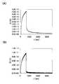
신뢰성을 조사하는 검사 방법으로서, 광을 조사하면서 트랜지스터의 게이트 전극과 소스 전극 사이의 전압(Vg)을 변화시켰을 때의 트랜지스터의 드레인 전극과 소스 전극 사이의 전류(Id)를 측정하여 얻어지는 트랜지스터의 Id-Vg 곡선을 측정한다. 또한, 산화물 반도체막을 이용한 트랜지스터에 있어서, 광을 조사하면서 -BT시험을 행하는, 즉 마이너스 게이트 스트레스를 인가하면 트랜지스터의 문턱값이 변화되는 열화가 있다. 이 열화를 광 네거티브 바이어스 열화라고도 부른다.(Id) of a transistor obtained by measuring a current (Id) between a drain electrode and a source electrode of the transistor when a voltage (Vg) between the gate electrode and the source electrode of the transistor is changed while irradiating light, Measure the -Vg curve. Further, in a transistor using an oxide semiconductor film, there is a deterioration in which the threshold value of the transistor is changed when -BT test is performed while light is applied, that is, negative gate stress is applied. This deterioration is also referred to as optical negative bias deterioration.
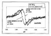
샘플 1, 2에 대한 광 네거티브 바이어스 열화를 도 11에 도시한다.The optical negative bias deterioration for
도 11에서 샘플 2는 샘플 1보다 Vth의 변화량이 작다.In Fig. 11, the variation of Vth is smaller than that of the
다음에, 샘플 1의 트랜지스터(L/W=3㎛/50㎛)에 600초간의 광(파장 400nm, 조사강도 3.5mW/㎠)을 조사하기 전후의 광응답성을 측정한 결과를 기초로 하여 광응답성의 그래프(광전류 시간의존성 그래프)를 작성한 결과를 도 12(A)에 도시한다. 또한, Vd는 0.1V이다.Next, on the basis of the result of measuring the light responsiveness before and after the irradiation of light (wavelength 400 nm, irradiation intensity 3.5 mW / cm 2) to the transistor (L / W = 3 탆 / 50 탆) of the
또한, 샘플 2의 트랜지스터(L/W=3㎛/50㎛)에 600초간의 광(파장 400nm, 조사강도 3.5mW/㎠)을 조사하기 전후의 광응답성을 측정한 결과를 기초로 하여 광응답성의 그래프(광전류 시간의존성 그래프)를 작성한 결과를 도 12(B)에 도시한다. 또한, Vd는 0.1V이다.On the basis of the result of measuring the light responsiveness before and after the irradiation of light (wavelength 400 nm, irradiation intensity 3.5 mW / cm 2) to the transistor (L / W = 3 탆 / 50 탆) of the
또한, 샘플 2와 제작 조건이 동일한 트랜지스터의 W폭을 크게 한 조건(L/W=30㎛/10000㎛)이나 샘플 2와 제작 조건이 동일한 트랜지스터의 W폭을 크게 한 조건에서 더 Vd를 더 크게 한 조건(Vd=15V)에서도 측정을 행하고, 피팅을 행하여 각각 2종류의 완화 시간(τ1과 τ2)을 표 1에 도시한다.Further, under the condition that the W width of the transistor having the same fabrication conditions as the
Vd=0.1VSample 1: L / W = 3/50,
Vd = 0.1 V
Vd=0.1VSample 2: L / W = 3/50,
Vd = 0.1 V
Vd=0.1VL / W = 30 / 100,000 mu m,
Vd = 0.1 V
Vd=15VL / W = 30 / 100,000 mu m,
Vd = 15V
또한, 2종류의 완화 시간(τ1과 τ2)은 트랩 밀도에 의존하고 있는 값이다. τ1과 τ2을 산출하는 방법을 광응답 결함 평가법이라고 부른다.The relaxation times (?1 and?2 ) of the two kinds depend on the trap density. The method of calculating τ1 and τ2 is called the optical response defect evaluation method.
표 1로부터, 샘플 1에 비해서 광 네거티브 바이어스 열화가 작은 샘플 2에서 광응답성이 빠른 것을 알 수 있다. 이로 인해, 광 네거티브 바이어스 열화가 작을수록 광응답성도 빠르다는 관계를 발견할 수 있다.It can be seen from Table 1 that
그 이유 중 하나를 설명한다. 만약 깊은 도너 준위가 존재하고, 도너 준위에 정공이 트랩되는 경우라면, 광 네거티브 바이어스 열화에서는 게이트에 인가된 마이너스 바이어스에 의해 고정 전하가 되고, 광응답에 있어서는 전류값의 완화시간을 증가시킬 가능성이 있다. 결정성 산화물 반도체막을 이용한 트랜지스터에서 광 네거티브 바이어스 열화가 작고 열응답성도 빠른 것은, 상기 정공을 트랩하는 도너 준위의 밀도가 작아져 있는 것에 기인하는 것으로 예상된다. 도 13에 예상되는 도너 준위의 모식도를 도시한다.Explain one of the reasons. If there is a deep donor level and holes are trapped in the donor level, the deterioration of the optical negative bias results in a fixed charge due to the negative bias applied to the gate, and the possibility of increasing the relaxation time of the current value in the optical response have. It is expected that the deterioration of the optical negative bias in the transistor using the crystalline oxide semiconductor film is small and the thermal response is also high because the density of the donor level trapping the holes is small. 13 shows a schematic diagram of the donor level expected in Fig.
또한, 도너 준위의 깊이나 밀도의 변화를 조사하기 위해서 저온 PL에 의해 측정을 행했다. 산화물 반도체막의 성막시의 기판 온도가 400℃인 경우와 산화물 반도체막의 성막시의 기판 온도가 200℃인 경우를 도 14에 도시한다.Further, in order to investigate the change of the depth or the density of the donor level, measurement was performed by low temperature PL. FIG. 14 shows the case where the substrate temperature at the time of forming the oxide semiconductor film is 400 ° C and the case where the substrate temperature at the time of forming the oxide semiconductor film is 200 ° C.
도 14에 의하면, 산화물 반도체막의 성막시의 기판 온도가 400℃인 경우에는 약 1.8eV 부근의 피크 강도가 기판 온도 200℃인 경우에 비해서 대폭적으로 감소되었다. 이 측정 결과는, 도너 준위의 깊이는 변하지 않고, 밀도가 대폭적으로 감소되어 있는 것을 시사하고 있다.According to Fig. 14, when the substrate temperature at the time of forming the oxide semiconductor film was 400 캜, the peak intensity around 1.8 eV was drastically reduced as compared with the case where the substrate temperature was 200 캜. This measurement result indicates that the depth of the donor level is not changed and the density is greatly reduced.
또한, 산화물 반도체막의 성막시의 기판 온도의 조건을 바꾸어서 각각 비교하여, 단일막에서의 평가를 행했다.The conditions of the substrate temperature at the time of film formation of the oxide semiconductor film were changed and compared with each other, and evaluation was performed on a single film.
샘플 A는 석영 기판(두께 0.5mm) 상에 50nm의 막 두께의 산화물 반도체막을 성막한 것이다. 또한, 산화물 반도체막의 성막 조건은 산화물 반도체용 타겟(In-Ga-Zn-O계 산화물 반도체용 타겟(In2O3 : Ga2O3 : ZnO = 1 : 1 : 2[mol수비])을 이용하여 기판과 타겟 사이의 거리를 170mm, 기판 온도 200℃, 압력 0.4Pa, 직류(DC) 전원 0.5kW, 아르곤(30sccm) 및 산소(15sccm)의 혼합 분위기하로 한다.Sample A was obtained by forming an oxide semiconductor film having a film thickness of 50 nm on a quartz substrate (thickness 0.5 mm). The oxide semiconductor film was formed under the same conditions as in the case of using a target for an oxide semiconductor (In2 O3 : Ga2 O3 : ZnO = 1: 1: 2 [molar ratio]) for In-Ga-Zn- And a distance between the substrate and the target is 170 mm, a substrate temperature is 200 占 폚, a pressure is 0.4 Pa, a direct current (DC) power is 0.5 kW, argon (30 sccm) and oxygen (15 sccm).
ESR(전자스핀 공명)을 실온(300K)에서 측정하고, 마이크로파(주파수 9.5GHz)의 흡수가 일어나는 자기장의 값(H0)으로부터 식 g=hv/βH0을 이용하여 g값이라는 파라미터가 얻어진다. 또한, h는 플랭크 정수이고, β는 보어 마그네톤이며, 이들은 모두 정수이다.The ESR (Electron Spin Resonance), the room temperature (300K) measurement, microwave (frequency 9.5GHz) parameters of g values using the equation g = hv / βH0 from a value (H0) of the magnetic field takes place in the absorption can be obtained. Also, h is the flange constant and beta is the bore magnetite, all of which are integers.
샘플 A의 g값을 나타내는 그래프를 도 15(A)에 도시한다.A graph showing the g value of the sample A is shown in Fig. 15 (A).
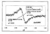
또한, 샘플 A와 동일한 조건에서 성막을 행한 후, 질소 분위기하에서 450℃로 1시간 가열한 것을 샘플 B라고 한다. 샘플 B의 g값을 나타내는 그래프를 도 15(B)에 도시한다.Further, after film formation was performed under the same conditions as Sample A, the sample was heated at 450 占 폚 for 1 hour under a nitrogen atmosphere. A graph showing the g value of the sample B is shown in Fig. 15 (B).
또한, 샘플 A와 동일한 조건에서 성막을 행한 후, 질소와 산소의 혼합분위기하에서 450℃로 1시간 가열한 것을 샘플 C라고 한다. 샘플 C의 g값을 나타내는 그래프를 도 15(C)에 도시한다.Sample C was obtained by performing film formation under the same conditions as Sample A and then heating it at 450 占 폚 for 1 hour in a mixed atmosphere of nitrogen and oxygen. A graph showing the g value of the sample C is shown in Fig. 15 (C).
샘플 B의 g값의 그래프에서 g=1.93의 시그널을 확인할 수 있고, 스핀 밀도는 1.8×10¹⁸[spins/㎤]로 되어 있었다. 한편, 샘플 C의 ESR의 결과에서는 g=1.93의 시그널을 확인할 수 없었으므로, g=1.93의 시그널은 산화물 반도체막 속의 메탈의 댕글링 본드에 기인한다.In the graph of the g value of the sample B, a signal of g = 1.93 was confirmed, and the spin density was 1.8 × 10¹⁸ [spins / cm 3]. On the other hand, since the signal of g = 1.93 was not confirmed in the result of the ESR of the sample C, the signal of g = 1.93 is caused by the dangling bond of the metal in the oxide semiconductor film.
또한, 샘플 D, E, F, G는 석영 기판(두께 0.5mm) 상에 막 두께 100nm의 산화물 반도체막을 성막한 것이다. 또한, 산화물 반도체막의 성막 조건은, 산화물 반도체용 타겟(In-Ga-Zn-O계 산화물 반도체용 타겟(In2O3 : Ga2O3 : ZnO = 1 : 1 : 2[mol수비])을 이용하여 기판과 타겟 사이의 거리를 170mm, 압력 0.4Pa, 직류(DC) 전원 0.5kW, 아르곤(30sccm) 및 산소(15sccm)의 혼합 분위기하로 한다. 또한, 샘플D, E, F, G는 각각 성막시의 기판 온도가 다르며, 샘플 D는 실온, 샘플 E는 200℃, 샘플 F는 300℃, 샘플 G는 400℃이다.Samples D, E, F, and G are obtained by forming an oxide semiconductor film having a thickness of 100 nm on a quartz substrate (thickness: 0.5 mm). The conditions for forming the oxide semiconductor film were as follows: a target for an oxide semiconductor (In2 O3 : Ga2 O3 : ZnO = 1: 1: 2 [molar ratio]) for an In-Ga-Zn- The distance between the substrate and the target is 170 mm, the pressure is 0.4 Pa, the direct current (DC) power is 0.5 kW, argon (30 sccm) and oxygen (15 sccm) The substrate temperature at the time of film formation is different, Sample D is room temperature, Sample E is 200 占 폚, Sample F is 300 占 폚, and Sample G is 400 占 폚.
샘플 D, E, F, G의 g값의 그래프를 나열하여 도 16에 도시했다.The graphs of the g values of the samples D, E, F and G are listed and shown in Fig.
성막시의 기판 온도가 400℃인 샘플 G에서는 g=1.93의 시그널을 확인할 수 있고, 스핀 밀도는 1.3×10¹⁸[spins/㎤]로 되어 있었다. 그 스핀 밀도는 샘플 B에서 얻어진 g=1.93의 시그널의 스핀 밀도와 동일한 정도이다.In the substrate temperature in film formation 400 ℃ Sample G can identify the signal of g = 1.93, the spin density was set to1.3 × 10 18 [spins / ㎤ ]. The spin density is about the same as the spin density of the signal of g = 1.93 obtained in the sample B. [
이들 결과로부터, 성막시의 기판 온도가 높아지면, 결정성의 향상이 원인인 것으로 생각되어지는 g값의 이방성의 증대가 확인되었다. 또한, g=1.93 시그널이 일어나는 원인이 되는 댕글링 본드는 막 두께 의존성을 가지며, IGZO의 벌크에 의존하고 있는 것이 시사된다.From these results, it was confirmed that an increase in the anisotropy of g value, which is considered to be the cause of the improvement in crystallinity, was confirmed when the substrate temperature at the time of film formation was increased. It is also suggested that the dangling bonds which cause g = 1.93 signals have film thickness dependence and depend on the bulk of IGZO.
샘플 B의 ESR 측정을 행한 것을 도시한 도 17에서는, 자기장을 기판표면에 대해서 수직으로 인가한 경우와 기판표면에 대해서 평행으로 인가한 경우의 g값의 차이(이방성)도 나타낸다.In Fig. 17 showing the ESR measurement of the sample B, there is also shown a difference (anisotropy) in g value when the magnetic field is applied perpendicularly to the substrate surface and when it is applied parallel to the substrate surface.
또한, 샘플 G와 동일한 조건에서 성막을 행한 후, 질소분위기하에서 450℃로 1시간 가열한 샘플 H의 ESR 측정을 행한 것을 도시한 도 18에서는, 자기장을 기판표면에 대해서 수직으로 인가한 경우와 기판표면에 대해서 평행으로 인가한 경우의 g값의 차이(이방성)도 나타낸다.18 showing the ESR measurement of the sample H heated at 450 DEG C for one hour in the nitrogen atmosphere after the film formation was performed under the same conditions as those of the sample G was compared with the case where the magnetic field was applied perpendicularly to the substrate surface, The difference in g value (anisotropy) when applied parallel to the surface is also shown.
도 17과 도 18을 비교한 결과, 기판 온도 200℃에서는 이방성에 의한 g값의 변화(Δg)가 0.001이하였던 것에 비해서, 기판 온도 400℃에서는 Δg가 0.003으로 증가되는 것을 알 수 있다. 일반적으로 결정성이 좋을수록(궤도의 방향이 일치할수록) 이방성이 커지는 것으로 알려져 있으며, 기판 온도 400℃의 막은 기판 온도 200℃의 막과 비교하여, 질소분위기하에서 450℃로 1시간 가열하여 발생하는 댕글링 본드의 방향이 일치하고 있다는 결론, 즉 결정성이 좋다는 결론에 이른다.As a result of comparison between Fig. 17 and Fig. 18, it can be seen that? G is increased to 0.003 at a substrate temperature of 400 占 폚, compared with a change in g value due to anisotropy (? G) of 0.001 or less at a substrate temperature of 200 占 폚. Generally, it is known that the better the crystallinity (the more the direction of the orbit coincides), the larger the anisotropy becomes. The film having a substrate temperature of 400 ° C is generated by heating for 1 hour at 450 ° C under a nitrogen atmosphere It is concluded that the directions of the dangling bonds are consistent, that is, the crystallinity is good.
또한, 산화물 반도체막의 막 두께 조건을 바꾸어서 ESR 측정을 행하여, g=1.93 시그널의 강도변화를 도 19 및 도 20에 도시한다. 도 19 및 도 20의 결과로부터, g=1.93 시그널의 강도는 산화물 반도체막의 막 두께의 증가에 따라서 증가되는 것이 확인되었다. 이것은, g=1.93 시그널을 일으키는 원인이 되는 댕글링 본드가 석영기판과 산화물 반도체막의 계면이나 산화물 반도체막 표면이 아니라 벌크에 존재하고 있는 것을 시사하고 있다.19 and 20 show changes in the intensity of the signal g = 1.93 by performing the ESR measurement while changing the film thickness condition of the oxide semiconductor film. From the results shown in Figs. 19 and 20, it was confirmed that the intensity of the signal of g = 1.93 increases with the increase of the film thickness of the oxide semiconductor film. This suggests that dangling bonds causing g = 1.93 signals are present in the bulk, rather than the interface between the quartz substrate and the oxide semiconductor film or the surface of the oxide semiconductor film.
이들 결과로부터, 메탈의 댕글링 본드는 이방성을 가지며, 그 이방성은, 성막온도가 높을수록 결정성이 좋기 때문에 커지는 것을 알 수 있다. 또한, 메탈의 댕글링 본드는 계면이나 표면이 아니라 벌크에 존재하는 것을 알 수 있다.From these results, it can be seen that the dangling bonds of the metal have anisotropy, and the anisotropy thereof becomes larger because the crystallinity is better the higher the film forming temperature. It can also be seen that the dangling bonds of the metal are present in the bulk, not the interface or the surface.
또한, 육방정 결정 구조를 갖는 제 1 재료막의 형성 프로세스 온도가 450℃ 이하인 경우에는 그 위에 형성하는 결정성 산화물 반도체막도 450℃ 이하로 형성할 수 있기 때문에 모유리와 같은 큰 기판을 이용하여 신뢰성이 높은 반도체 장치의 대량 생산을 행할 수 있다.
When the forming temperature of the first material film having the hexagonal crystal structure is 450 캜 or lower, the crystalline oxide semiconductor film to be formed thereon can also be formed at 450 캜 or lower. Therefore, a reliable substrate It is possible to mass-produce this high semiconductor device.
본 발명에 의하면, 산화물 반도체막을 이용한 반도체 장치에 안정된 전기적 특성을 부여하고, 신뢰성이 높은 반도체 장치를 제작할 수 있다.
According to the present invention, it is possible to manufacture a semiconductor device with high reliability by giving stable electrical characteristics to the semiconductor device using the oxide semiconductor film.
도 1은 본 발명의 일 양태를 도시한 단면도이다.
도 2는 본 발명의 일 양태를 도시한 단면도이다.
도 3은 본 발명의 일 양태를 도시한 단면도이다.
도 4는 본 발명의 일 양태를 도시한 단면도이다.
도 5는 본 발명의 일 양태를 도시한 단면도 및 상면도이다.
도 6은 섬유아연석형 결정 구조의 모식도이다.
도 7은 코런덤형 결정 구조의 모식도이다.
도 8은 본 발명의 일 양태를 제작하는 제조장치의 상면도의 일례이다.
도 9는 본 발명의 일 양태를 도시한 블록도 및 등가회로도이다.
도 10은 본 발명의 일 양태를 도시한 전자 기기의 외관도이다.
도 11은 광 네거티브 바이어스 열화를 설명하는 도면이다.
도 12는 광전류 시간의존성 그래프를 설명하는 도면이다.
도 13은 도너 준위를 설명하는 모식도이다.
도 14는 저온 PL의 측정결과를 설명하는 도면이다.
도 15는 ESR의 측정결과를 설명하는 도면이다.
도 16은 ESR의 측정결과를 설명하는 도면이다.
도 17은 ESR의 측정결과를 설명하는 도면이다.
도 18은 ESR의 측정결과를 설명하는 도면이다.
도 19는 ESR의 측정결과를 설명하는 도면이다.
도 20은 ESR로부터 얻어진 전체 스핀 수와 산화물 반도체층의 막 두께와의 관계를 설명하는 그래프이다.1 is a cross-sectional view showing one embodiment of the present invention.
2 is a cross-sectional view showing one embodiment of the present invention.
3 is a cross-sectional view showing one embodiment of the present invention.
4 is a cross-sectional view showing one embodiment of the present invention.
5 is a cross-sectional view and a top view showing one embodiment of the present invention.
Fig. 6 is a schematic diagram of a fibrous zinc silicate type crystal structure.
7 is a schematic diagram of a corundum-type crystal structure.
8 is an example of a top view of a manufacturing apparatus for manufacturing an embodiment of the present invention.
9 is a block diagram and an equivalent circuit diagram showing an embodiment of the present invention.
10 is an external view of an electronic device showing an embodiment of the present invention.
11 is a view for explaining optical negative bias deterioration.
12 is a diagram for explaining a photocurrent time dependency graph.
13 is a schematic diagram for explaining the donor level.
14 is a view for explaining measurement results of the low temperature PL.
15 is a view for explaining the measurement results of the ESR.
16 is a view for explaining the measurement results of the ESR.
17 is a view for explaining the measurement results of the ESR.
18 is a view for explaining the measurement result of the ESR.
19 is a view for explaining the measurement result of the ESR.
20 is a graph for explaining the relationship between the total spin number obtained from the ESR and the film thickness of the oxide semiconductor layer.
이하에서는 본 발명의 실시형태에 대해서 도면을 이용하여 상세하게 설명한다. 단, 본 발명은 이하의 설명에 한정되지 않고, 그 형태 및 상세를 다양하게 변경할 수 있는 것은 당업자라면 용이하게 이해할 수 있다. 또한, 본 발명은 이하에 나타내는 실시형태의 기재 내용에 한정되어 해석되는 것이 아니다.
Hereinafter, embodiments of the present invention will be described in detail with reference to the drawings. However, the present invention is not limited to the following description, and it is easily understood by those skilled in the art that various changes can be made in form and detail. The present invention is not limited to the description of the embodiments described below.
(실시형태 1)(Embodiment 1)
본 실시형태에서는 반도체 장치의 구조 및 제작 방법에 대해서 도 1을 이용하여 설명한다.In the present embodiment, a structure and a manufacturing method of a semiconductor device will be described with reference to Fig.
도 1(E)는 탑 게이트형 트랜지스터(120)의 단면도이며, 트랜지스터(120)는 절연 표면을 갖는 기판(100) 상에 산화물 절연층(101), 채널 형성 영역을 포함하는 반도체 적층, 소스 전극층(104a), 드레인 전극층(104b), 게이트 절연층(102), 게이트 전극층(112), 절연막(110a)을 포함한다. 반도체 적층의 단부를 덮어서 소스 전극층(104a) 및 드레인 전극층(104b)이 마련되고, 소스 전극층(104a) 및 드레인 전극층(104b)을 덮는 게이트 절연층(102)은 반도체 적층의 일부에 접한다. 이 반도체 적층의 일부 상에 게이트 절연층(102)을 사이에 두고 게이트 절연층(112)이 마련된다.1 (E) is a cross-sectional view of a top
또한, 절연막(110a)을 덮어서 절연막(110b)이 마련되어 있다.Further, an insulating
이하에 도 1(A) 내지 도 1(E)를 이용하여 기판 상에 트랜지스터(120)를 제작하는 공정을 설명한다.Hereinafter, the process of manufacturing the
우선, 기판(100) 상에 산화물 절연층(101)을 형성한다.First, an
기판(100)은 퓨전법이나 플로트법으로 제작되는 무알칼리 유리 기판, 본 제작 공정의 처리 온도에 견딜 수 있는 내열성을 갖는 플라스틱 기판 등을 이용할 수 있다. 또한, 스테인리스 등의 금속 기판의 표면에 절연막을 마련한 기판이나, 반도체 기판의 표면에 절연막을 마련한 기판을 적용해도 된다. 기판(100)이 모유리인 경우, 기판의 크기는 제 1 세대(320mm×400mm), 제 2 세대(400mm×500mm), 제 3 세대(550mm×650mm), 제 4 세대(680mm×880mm 또는 730mm×920mm), 제 5 세대(1000mm×1200mm 또는 1100mm×1250mm), 제 6 세대(1500mm×1800mm), 제 7 세대(1900mm×2200mm), 제 8 세대(2160mm×2460mm), 제 9 세대(2400mm×2800mm 또는 2450mm×3050mm), 제 10 세대(2950mm×3400mm) 등을 이용할 수 있다. 모유리는 처리 온도가 높고 처리 시간이 길면 대폭적으로 수축되기 때문에, 모유리를 사용하여 대량 생산을 행하는 경우, 제작 공정의 가열 처리는 600℃ 이하, 바람직하게는 450℃ 이하에서 행하는 것이 바람직하다.The
산화물 절연층(101)은 PCVD법 또는 스퍼터링법을 이용하여 50nm 이상 600nm 이하의 막 두께로 산화 실리콘막, 산화 갈륨막, 산화 알루미늄막, 산화질화 실리콘막, 산화질화 알루미늄막 또는 질화산화 실리콘막으로부터 선택된 한 층 또는 이들의 적층을 이용한다. 하지 절연층으로서 이용되는 산화물 절연층(101)은 막 속(벌크 속)에 적어도 화학양론비를 초과하는 양의 산소가 존재하는 것이 바람직하고, 예를 들어 산화 실리콘막을 이용하는 경우에는 SiO2+α(단 α>0)으로 한다. 산화물 절연층(101)의 막 두께를 두껍게 함으로써, 추후에 행해지는 가열 처리에서의 산화물 절연층(101)의 산소방출량을 증가시킬 수 있음과 동시에, 그 증가에 의해 산화물 절연층(101)과 추후에 형성되는 산화물 반도체막의 계면에서의 결함을 저감시킬 수 있다.The
또한, 알칼리 금속 등의 불순물을 포함하는 유리 기판을 이용하는 경우, 알칼리 금속의 침입을 방지하기 위해서, 산화물 절연층(101)과 기판(100) 사이에 질화물 절연층으로서 PCVD법 또는 스퍼터링법으로 얻어지는 질화 실리콘막, 질화 알루미늄막 등을 형성해도 된다. Li이나 Na 등의 알칼리 금속은 불순물이기 때문에 함유량을 감소시키는 것이 바람직하다.When a glass substrate containing an impurity such as an alkali metal is used, it is preferable to form a nitride (nitride) insulating layer between the
다음에, 산화물 절연층(101) 상에 막 두께 1nm 이상 10nm 이하의 제 1 재료막(118)을 형성한다(도 1(A) 참조).Next, a
본 실시형태에서는, 제 1 재료막(118)으로서 분자선 에피택시법(MBE법)을 이용하여 갈륨과 플라즈마에 의해 생성한 활성 질소를 이용하여 육방정 구조의 질화 갈륨막을 얻는다. 또한, 육방정 구조의 질화 갈륨막이 얻어지는 것이면 MBE법에 한정되지 않고, 트리메틸갈륨과 암모니아 가스를 원료로 하고, 질소 가스 등을 캐리어 가스로 하여 유기금속기상 에피택시법(MOCVD법)을 이용하여 육방정 구조의 질화 갈륨막을 형성할 수도 있다. 이 제 1 재료막(118)은 a-b면에서 육각형의 격자를 갖는 결합을 갖고, a-b면에 대략 평행한 기판 평면에 대략 수직인 c축을 가지고 있는 육방정 구조의 질화 갈륨 결정을 가지고 있으며, 종결정이 된다. 또한, 종결정은 a-b면에서 육각형의 격자를 갖는 결합을 갖는 층을 c축 방향으로 1원자층 이상 포함한다.In this embodiment, a gallium nitride film having a hexagonal crystal structure is obtained by using active nitrogen generated by gallium and plasma using a molecular beam epitaxy method (MBE method) as the
다음에, 대기에 접촉하지 않으며, 이 제 1 재료막(118)을 종결정으로서 이용하고, 그 위에 제 2 재료막, 즉 육방정 구조의 결정을 갖는 결정성 산화물 반도체막(108)을 형성한다(도 1(B) 참조). 제 2 재료막의 막 두께는 제 1 재료막의 막 두께보다 두껍게 하고, 예를 들어 10nm보다 두꺼운 막 두께로 한다.Next, the
본 실시형태에서는, 제 2 재료막을 산화물 반도체용 타겟(In-Ga-Zn-O계 산화물 반도체용 타겟(In2O3 : Ga2O3 : ZnO = 1 : 1 : 2[mol수비])을 이용하여 기판과 타겟 사이의 거리를 170mm, 기판 온도 400℃, 압력 0.4Pa, 직류(DC) 전원 0.5kW, 산소만, 아르곤만, 또는 아르곤 및 산소의 분위기하에서 형성하고, 막 두께 25nm의 결정성 산화물 반도체막(108)을 얻는다.In this embodiment, the second material film is an oxide semiconductor for a target (In-Ga-ZnO based oxide semiconductor target for(In 2 O 3: Ga 2 O 3: ZnO = 1: 1: 2 [mol defense]) for , A distance between the substrate and the target was 170 mm, the substrate temperature was 400 占 폚, the pressure was 0.4 Pa, the direct current (DC) power was 0.5 kW, oxygen alone, argon alone or argon and oxygen. An
제 2 재료막의 성막에 있어서, 스퍼터링 가스는 희가스(대표적으로는 아르곤), 산소, 희가스 및 산소의 혼합 가스를 적절히 이용한다. 또한, 스퍼터링 가스에는 수소, 물, 수산기 또는 수소화물 등의 불순물이 제거된 고순도 가스를 이용하는 것이 바람직하다. 또한, 제 2 재료막을 성막하는 처리실의 압력을 0.4Pa 이하로 함으로써, 결정성 산화물 반도체막의 표면 및 막 속으로의 알칼리 금속, 수소 등의 불순물의 혼입을 저감시킬 수 있다. 또한, 제 2 재료막을 성막하는 처리실의 누설량을 1×10⁻¹⁰Paㆍ㎥/초 이하로 함으로써, 스퍼터링법에 의한 성막 도중의 결정성 산화물 반도체막으로의 알칼리 금속, 수소, 물, 수산기 또는 수소화물 등의 불순물의 혼입을 저감시킬 수 있다. 또한, 배기계로서 흡착형 진공 펌프를 이용함으로써, 배기계로부터 알칼리 금속, 수소, 물, 수산기 또는 수소화물 등의 불순물의 역류를 저감시킬 수 있다. 또한, 제 2 재료막을 성막하기 위한 타겟의 순도를 99.99% 이상으로 함으로써, 결정성 산화물 반도체막에 혼입되는 알칼리 금속, 수소, 물, 수산기 또는 수소화물 등을 저감시킬 수 있다. 또한, 이 타겟을 이용함으로써, 결정성 산화물 반도체막에서 리튬의 농도를 5×1015cm-3 이하, 바람직하게는 1×1015cm-3 이하로 하고, 나트륨의 농도를 5×1016cm-3 이하, 바람직하게는 1×1016cm-3 이하, 더 바람직하게는 1×1015cm-3 이하로 하고, 칼륨의 농도를 5×1015cm-3 이하, 바람직하게는 1×1015cm-3 이하로 할 수 있다.In the film formation of the second material film, a mixed gas of rare gas (typically argon), oxygen, rare gas and oxygen is suitably used as the sputtering gas. It is also preferable to use a high-purity gas from which impurities such as hydrogen, water, hydroxyl, or hydride are removed from the sputtering gas. In addition, mixing of impurities such as alkali metals and hydrogen into the surface of the crystalline oxide semiconductor film and the film can be reduced by setting the pressure in the treatment chamber for forming the second material film to 0.4 Pa or less. Further, by setting the leakage amount of the processing chamber for forming the second material film to 1 10 <-10 > Pa < 3 > / sec / second or less, alkali metal, hydrogen, water, It is possible to reduce the incorporation of impurities such as pyrolysis. Further, by using an adsorption-type vacuum pump as the exhaust system, backflow of impurities such as alkali metal, hydrogen, water, hydroxyl, or hydride from the exhaust system can be reduced. Further, by setting the purity of the target for film formation of the second material film to 99.99% or more, the alkali metal, hydrogen, water, hydroxyl group, hydride, etc. mixed into the crystalline oxide semiconductor film can be reduced. Further, by using this target, the concentration of lithium in the crystalline oxide semiconductor film is set to 5 × 1015 cm-3 or less, preferably 1 × 1015 cm-3 or less, and the concentration of sodium is set to 5 × 1016 cm-3 or less, preferably 1 × 1016 cm-3 or less, more preferably 1 × 1015 cm-3 or less, and the concentration of potassium is 5 × 1015 cm-3 or less, preferably 1 × 1015 cm-3 or less, It can be less than15 cm-3.
알칼리 금속 및 알칼리 토류 금속은 결정성 산화물 반도체막에 있어서 악성의 불순물이므로 적은 것이 좋다. 특히 알칼리 금속 중 나트륨은 결정성 산화물 반도체에 접하는 산화물 절연막으로 확산되어 Na+가 된다. 또한, 결정성 산화물 반도체 내에서 금속과 산소의 결합을 분단시키거나 결합 속으로 들어간다. 그 결과, 트랜지스터 특성의 열화(예를 들어 노멀리 온화(문턱값의 마이너스로의 시프트), 이동도의 저하 등)를 초래한다. 아울러, 특성의 변동의 원인이 되기도 한다. 이와 같은 문제는 특히 결정성 산화물 반도체막 속의 수소의 농도가 충분히 낮은 경우에 현저해진다. 따라서, 결정성 산화물 반도체막 속의 수소의 농도가 5×1019cm-3 이하, 특히 5×1018cm-3 이하인 경우에는 알칼리 금속의 농도를 상기와 같은 값으로 하는 것이 강하게 요구되어진다.It is preferable that the alkali metal and alkaline earth metal are malignant impurities in the crystalline oxide semiconductor film. Particularly, sodium in the alkali metal diffuses into the oxide insulating film in contact with the crystalline oxide semiconductor and becomes Na+ . In addition, it breaks the bond of the metal and oxygen in the crystalline oxide semiconductor or enters into the bond. As a result, deterioration of the transistor characteristics (for example, normalization (shift to a negative value of the threshold), decrease of mobility, etc.) is caused. In addition, it may cause fluctuation of characteristics. This problem becomes conspicuous particularly when the concentration of hydrogen in the crystalline oxide semiconductor film is sufficiently low. Therefore, when the concentration of hydrogen in the crystalline oxide semiconductor film is not more than 5 × 1019 cm-3 , particularly not more than 5 × 1018 cm-3 , it is strongly required to set the concentration of alkali metal to the same value as described above.
또한, 제 2 재료막의 성막시에 기판을 기판 지지체에 마련되는 히터에 의해 250℃ 이상 기판의 열처리 상한 온도 이하로 가열한다. 따라서, 성막 중에 종결정을 핵으로 이용하여, 피성막 표면에 퇴적되는 원자가 산화되면서 결정 성장을 하기 때문에 결정성 산화물 반도체막(108)을 제작할 수 있다.Further, at the time of forming the second material film, the substrate is heated to a temperature not higher than the upper limit of the heat treatment temperature of the substrate by not less than 250 占 폚 by a heater provided on the substrate support. Therefore, the crystalline
이상의 조건에 의해, 결정성 산화물 반도체막을 형성함으로써, 알칼리 금속의 농도를 5×10¹⁶ atoms/㎤ 이하, 수소의 농도를 1×10¹⁹ atoms/㎤ 이하로 한, 불순물을 극히 저감시킨 결정성 산화물 반도체막을 형성할 수 있다. 결정성 산화물 반도체막의 불순물을 저감시킴으로써, 종결정 및 결정성 산화물 반도체막의 결정성장이 촉진되어, 단결정 또는 실질적으로 단결정인 결정성 산화물 반도체막을 형성할 수 있다. 이 결정성 산화물 반도체막(108)은 비정질 구조가 아니며, 결정성 구조, 이상적으로는 단결정 구조이며, 기판평면에 대략 수직인 c축을 가진 구조(C Axis Alligned Crystal : CAAC라고도 부른다.)를 포함하는 산화물을 갖는다.By forming the crystalline oxide semiconductor film by the above-described conditions, a crystalline oxide having an extremely low impurity concentration with an alkali metal concentration of 5 x 10¹⁶ atoms / cm 3 or less and a hydrogen concentration of 1 x 10¹⁹ atoms / A semiconductor film can be formed. By reducing the impurities of the crystalline oxide semiconductor film, the crystal growth of the seed crystal and the crystalline oxide semiconductor film is promoted, and a single crystal or substantially single crystal crystalline oxide semiconductor film can be formed. The crystalline
다음에, 기판을 배치하는 챔버 분위기를 질소 또는 건조 공기로 하여 가열 처리를 행한다. 가열 처리의 온도는 400℃ 이상 750℃ 이하로 한다. 또한, 가열 처리의 가열 시간은 1분 이상 24시간 이하로 한다.Next, the chamber atmosphere in which the substrate is placed is subjected to heat treatment with nitrogen or dry air. The temperature of the heat treatment should be 400 ° C or more and 750 ° C or less. The heating time for the heat treatment is 1 minute to 24 hours.
또한, 산화물 절연층(101)의 형성으로부터 가열 처리까지의 공정을 대기에 접촉하지 않고 연속적으로 행하는 것이 바람직하다. 예를 들어 도 8의 상면도에 도시한 제조 장치를 이용하면 된다. 도 8에 도시한 제조 장치는 매엽식 멀티 챔버장치이며, 3개의 성막 장치(10a, 10b, 10c)나, 피처리기판을 수용하는 카세트 포트(14)를 3개 갖는 기판 공급실(11)이나, 로드 로크실(12a, 12b)이나, 반송실(13)이나, 기판 가열실(15) 등을 가지고 있다. 또한, 기판 공급실(11) 및 반송실(13)에는 피처리기판을 반송하기 위한 반송 로봇이 각각 배치되어 있다. 성막장치(10a, 10b, 10c), 반송실(13) 및 기판 가열실(15)은 수소 및 수분을 거의 포함하지 않는 분위기(비활성분위기, 감압분위기, 건조 공기 분위기 등)하에서 제어하는 것이 바람직하고, 예를 들어 수분에 대해서는 이슬점 -40℃ 이하, 바람직하게는 이슬점 -50℃ 이하의 건조 질소 분위기로 한다. 도 8의 제조 장치를 이용한 제작 공정의 절차의 일례는, 우선 기판 공급실(11)로부터 피처리기판을 반송하고, 로드 로크실(12a)과 반송실(13)을 거쳐서 기판 가열실(15)로 이동시키고, 기판 가열실(15)에서 피처리기판에 부착되어 있는 수분을 진공 베이크 등으로 제거하고, 그 후에 반송실(13)을 거쳐서 성막장치(10c)에 피처리기판을 이동시키고, 성막 장치(10c) 내에서 산화물 절연층(101)을 성막한다. 그리고, 대기에 접촉하지 않으며, 반송실(13)을 거쳐서 성막 장치(10a)에 피처리기판을 이동시키고, 성막 장치(10a) 내에서 막 두께 5nm의 제 1 재료막(118)을 성막한다. 그리고 대기에 접촉하지 않으며, 반송실(13)을 거쳐서 성막 장치(10b)에 피처리기판을 이동시키고, 성막 장치(10b) 내에서 막 두께 10nm보다 두꺼운 결정성 산화물 반도체막(108)을 성막한다. 그리고, 대기에 접촉하지 않으며, 반송실(13)을 거쳐서 기판 가열실(15)에 피처리기판을 이동시켜서 가열 처리를 행한다. 이와 같이, 도 8의 제조 장치를 이용함으로써 대기에 접촉하지 않으며, 제작프로세스를 진행시킬 수 있다.Further, it is preferable that the steps from the formation of the
다음에, 제 1 재료막(118)과 결정성 산화물 반도체막(108)으로 이루어진 반도체 적층을 가공하여 섬형의 반도체 적층을 형성한다. 도면에서는, 제 1 재료막(118)과 결정성 산화물 반도체막(108)은 재료가 다르기 때문에, 계면을 실선으로 나타내고, 적층으로 설명하고 있으나, 추후의 열처리 등에 의해 계면이 불명료해지는 경우도 있다. 또한, 제 1 재료막으로서 α-Ga2O3, In2O3를 이용하는 경우에는 결정성 산화물 반도체막(108)과 재료가 일부 동일하기 때문에, 계면이 불명료해지는 경우도 있다.Next, a semiconductor laminate composed of the
반도체 적층의 가공은 원하는 형상의 마스크를 반도체 적층 상에 형성한 후, 이 반도체 적층을 에칭함으로써 행할 수 있다. 상술한 마스크는 포토리소그래피 등의 방법을 이용하여 형성할 수 있다. 또는 잉크젯법 등의 방법을 이용하여 마스크를 형성해도 된다.Semiconductor stacking can be performed by forming a mask of a desired shape on a semiconductor stack, and then etching the semiconductor stack. The above-described mask can be formed by a method such as photolithography. Alternatively, a mask may be formed by a method such as an inkjet method.
또한, 반도체 적층의 에칭은 드라이 에칭이어도 웨트 에칭이어도 된다. 물론 이들을 조합시켜서 이용해도 된다.The etching of the semiconductor laminate may be dry etching or wet etching. Of course, they may be used in combination.
다음에, 반도체 적층 상에 소스 전극층 및 드레인 전극층(이와 동일한 층으로 형성되는 배선을 포함함)을 형성하기 위한 도전막을 형성하고, 이 도전막을 가공하여 소스 전극층(104a) 및 드레인 전극층(104b)을 형성한다(도 1(C) 참조). 소스 전극층(104a) 및 드레인 전극층(104b)은 스퍼터링법 등에 의해 몰리브덴, 티탄, 탄탈, 텅스텐, 알루미늄, 구리, 네오듐, 스칸듐 등의 금속 재료 또는 이들을 주성분으로 하는 합금 재료를 이용하여 단층으로 또는 적층하여 형성할 수 있다.Next, a conductive film for forming a source electrode layer and a drain electrode layer (including wirings formed of the same layer) is formed on the semiconductor laminate, and the conductive film is processed to form the
다음에, 반도체 적층의 일부와 접하고, 또한, 소스 전극층(104a) 및 드레인 전극층(104b)을 덮는 게이트 절연층(102)을 형성한다(도 1(D) 참조). 게이트 절연층(102)은 플라즈마 CVD법 또는 스퍼터링법 등을 이용하여 형성한 산화물 절연층이며, 산화 실리콘, 산화질화 실리콘, 질화산화 실리콘, 산화 알루미늄, 산화 갈륨, 산화질화 알루미늄, 질화산화 알루미늄, 산화 하프늄, 또는 이들의 혼합 재료를 이용하여 단층으로 또는 적층하여 형성한다. 게이트 절연층(102)의 막 두께는 10nm 이상 200nm 이하이다.Next, a
본 실시형태에서는, 게이트 절연층(102)로서, 스퍼터링법을 이용하여 100nm의 산화 실리콘막을 형성한다. 그리고 게이트 절연층(102)의 형성 후에 제 2 가열 처리를 행한다. 제 2 가열 처리의 조건은, 비활성 분위기, 산소 분위기, 산소와 질소의 혼합 분위기하에서 200℃ 이상 400℃ 이하로 한다. 또한, 제 2 가열 처리의 가열 시간은 1분 이상 24시간 이하로 한다. 제 2 가열 처리에 의해 게이트 절연층(102)으로부터 반도체 적층으로의 산소 공급이 행해지고, 가열 처리 온도가 높을수록 광을 조사하면서 -BT시험을 행했을 때의 문턱값의 변화량은 억제된다.In this embodiment, as the
다음에, 게이트 절연층(102) 상에 도전막을 형성한 후, 포토리소그래피 공정에 의해 게이트 전극층(112)을 형성한다. 게이트 전극층(112)은 게이트 절연층(102)을 사이에 두고 반도체 적층의 일부와 겹쳐진다. 게이트 전극층(112)을 형성하기 위한 도전막은, 스퍼터링법 등에 의해 몰리브덴, 티탄, 탄탈, 텅스텐, 알루미늄, 구리, 네오듐, 스칸듐 등의 금속 재료 또는 이들을 주성분으로 하는 합금재료를 이용하여 단층으로 또는 적층하여 형성할 수 있다.Next, a conductive film is formed on the
다음에, 게이트 전극층(112) 및 게이트 절연층(102)을 덮는 절연막(110a), 절연막(110b)을 형성한다(도 1(E) 참조).Next, an insulating
절연막(110a) 및 절연막(110b)은 산화 실리콘, 질화 실리콘, 산화 갈륨, 산화질화 실리콘, 질화산화 실리콘, 산화 알루미늄, 질화 알루미늄, 산화질화 알루미늄, 질화산화 알루미늄, 산화 하프늄, 또는 이들의 혼합 재료를 이용하여 단층으로 또는 적층하여 형성할 수 있다. 본 실시형태에서는 절연막(110a)으로서 스퍼터링법으로 얻어지는 300nm의 산화 실리콘막을 이용하여 질소 분위기하에서 250℃로 1시간 가열 처리를 행한다. 그 후, 수분의 침입 방지나 알칼리 금속의 침입방지를 위해서, 절연막(110b)으로서 스퍼터링법으로 얻어지는 질화 실리콘막을 형성한다. Li이나 Na 등의 알칼리 금속은 불순물이기 때문에 함유량을 적게 하는 것이 바람직하며, 반도체 적층 속에 2×1016cm-3 이하, 바람직하게는 1×1015cm-3 이하의 농도로 한다. 또한, 본 실시형태에서는 절연막(110a) 및 절연막(110b)의 2층구조로 하는 예를 도시했으나, 단층 구조로 해도 된다.The insulating
이상의 공정으로 탑 게이트형 트랜지스터(120)가 형성된다. a-b면에서 육각형의 격자를 갖는 결합을 갖고, a-b면에 대략 평행인 기판 평면에 대략 수직인 c축을 갖는 육방정 구조의 결정을 포함하는 결정성 산화물 반도체막을 채널 영역에 갖는 트랜지스터(120)는 광조사나 BT 시험 전후의 문턱값 전압의 변화량이 적기 때문에 안정된 전기적 특성을 갖는다.
The top
(실시형태 2)(Embodiment 2)
본 실시형태에서는 실시형태 1과 일부 다른 공정예를 도 2를 사용하여 설명한다. 또한, 도 2에서 도 1과 동일한 부분에는 동일한 부호를 사용하고, 동일한 부호의 상세한 설명은 여기서는 생략한다.In this embodiment, a process example that is different from the first embodiment will be described with reference to Fig. In Fig. 2, the same reference numerals are used for the same parts as those in Fig. 1, and detailed descriptions of the same reference numerals are omitted here.
도 2(D)는 탑 게이트형 트랜지스터(130)의 단면도이며, 트랜지스터(130)는 절연 표면을 갖는 기판(100) 상에 산화물 절연층(101), 소스 전극층(104a), 드레인 전극층(104b), 채널 형성 영역을 포함하는 반도체 적층, 게이트 절연층(102), 게이트 전극층(112), 절연막(110a)을 포함한다. 소스 전극층(104a) 및 드레인 전극층(104b)을 덮어서 반도체 적층이 마련된다. 이 반도체 적층의 일부 상에 게이트 절연층(102)을 사이에 두고 게이트 절연층(112)이 마련된다.2 (D) is a cross-sectional view of the top
또한, 절연막(110a)을 덮어서 절연막(110b)이 마련되어 있다.Further, an insulating
이하에 도 2(A) 내지 도 2(D)를 이용하여, 기판 상에 트랜지스터(130)를 제작하는 공정을 설명한다.Hereinafter, the steps of fabricating the
우선, 기판(100) 상에 산화물 절연층(101)을 형성한다.First, an
다음에, 산화물 절연층(101) 상에 소스 전극층 및 드레인 전극층(이와 동일한 층에서 형성되는 배선을 포함함)을 형성하기 위한 도전막을 형성하고, 이 도전막을 가공하여 소스 전극층(104a) 및 드레인 전극층(104b)을 형성한다.Next, a conductive film for forming a source electrode layer and a drain electrode layer (including wiring formed in the same layer) is formed on the
다음에, 소스 전극층(104a) 및 드레인 전극층(104b) 상에 막 두께 1nm 이상 10nm 이하의 제 1 재료막(118)을 형성한다(도 2(A) 참조).Next, a
다음에, 제 1 재료막(118) 상에 10nm보다 두꺼운 결정성 산화물 반도체막(108)을 형성한다(도 2(B) 참조).Next, a crystalline
다음에, 기판을 배치하는 분위기를 질소 또는 건조 공기로 하여 가열 처리를 행한다. 가열 처리의 온도는 400℃ 이상 750℃ 이하로 한다.Next, the atmosphere in which the substrate is placed is subjected to heat treatment with nitrogen or dry air. The temperature of the heat treatment should be 400 ° C or more and 750 ° C or less.
다음에, 필요하다면 제 1 재료막(118)과 결정성 산화물 반도체막(108)으로 이루어진 반도체 적층을 가공하여 섬형의 반도체 적층을 형성한다.Next, if necessary, a semiconductor laminate composed of the
다음에, 반도체 적층 상에 게이트 절연층(102)을 형성한다(도 2(C) 참조).Next, a
다음에, 게이트 절연층(102) 상에 도전막을 형성한 후, 포토리소그래피 공정에 의해 게이트 전극층(112)을 형성한다. 게이트 전극층(112)은 게이트 절연층(102)을 사이에 두고 반도체 적층의 일부와 겹쳐진다.Next, a conductive film is formed on the
다음에, 게이트 전극층(112) 및 게이트 절연층(102)을 덮는 절연막(110a), 절연막(110b)을 형성한다(도 2(D) 참조).Next, an insulating
이상의 공정으로 탑 게이트형 트랜지스터(130)가 형성된다.The top
도 2(D)에 도시한 트랜지스터(130)에 있어서도, a-b면에서 육각형의 격자를 갖는 결합을 갖고, a-b면에 대략 평행인 기판 평면에 대략 수직인 c축을 갖는 육방정 구조의 결정을 포함하는 결정성 산화물 반도체막을 채널 영역에 가지므로, 트랜지스터(130)는 광조사나 BT 시험 전후의 문턱값 전압의 변화량이 적기 때문에 안정된 전기적 특성을 갖는다.The
본 실시형태는 실시형태 1과 자유롭게 조합시킬 수 있다.
This embodiment mode can be freely combined with the first embodiment mode.
(실시형태 3)(Embodiment 3)
본 실시형태에서는 실시형태 1과 일부 다른 공정예를 도 3을 이용하여 설명한다. 또한, 도 3에서 도 1과 동일한 부분에는 동일한 부호를 이용하고, 동일한 부호의 상세한 설명은 여기서는 생략한다.In this embodiment, a process example that is different from the first embodiment will be described with reference to Fig. In Fig. 3, the same reference numerals are used for the same parts as in Fig. 1, and the detailed description of the same reference numerals is omitted here.
도 3(F)는 보텀 게이트형 트랜지스터(140)의 단면도이며, 트랜지스터(140)는 절연 표면을 갖는 기판(100) 상에 산화물 절연층(101), 게이트 전극층(112), 게이트 절연층(102), 소스 전극층(104a), 드레인 전극층(104b), 채널 형성 영역을 포함하는 반도체 적층, 절연막(110a)을 포함한다. 소스 전극층(104a) 및 드레인 전극층(104b)을 덮어서 반도체 적층이 마련된다. 이 반도체 적층에서, 게이트 절연층(102)을 사이에 두고 게이트 전극층(112)과 겹쳐지는 영역의 일부가 채널 형성 영역으로서 기능한다.3 (F) is a cross-sectional view of the bottom
또한, 절연막(110a)을 덮어서 절연막(110b)이 마련되어 있다.Further, an insulating
이하에 도 3(A) 내지 도 3(F)를 이용하여, 기판 상에 트랜지스터(140)를 제작하는 공정을 설명한다.Hereinafter, the steps of manufacturing the
우선, 기판(100) 상에 산화물 절연층(101)을 형성한다.First, an
다음에, 산화물 절연층(101) 상에 도전막을 형성한 후, 포토리소그래피공정에 의해 게이트 전극층(112)을 형성한다.Next, a conductive film is formed on the
다음에, 게이트 전극층(112) 상에 게이트 절연층(102)을 형성한다(도 3(A) 참조).Next, a
다음에, 게이트 절연층(102) 상에 소스 전극층 및 드레인 전극층(이와 동일한 층으로 형성되는 배선을 포함함)을 형성하기 위한 도전막을 형성하고, 이 도전막을 가공하여 소스 전극층(104a) 및 드레인 전극층(104b)을 형성한다(도 3(B) 참조).Next, a conductive film is formed on the
다음에, 소스 전극층(104a) 및 드레인 전극층(104b) 상에 막 두께 1nm 이상 10nm 이하의 제 1 재료막(118)을 형성한다(도 3(C) 참조).Next, a
다음에, 제 1 재료막(118) 상에 10nm보다 두꺼운 결정성 산화물 반도체막(108)을 형성한다(도 3(D) 참조).Next, a crystalline
다음에, 기판을 배치하는 분위기를 질소 또는 건조 공기로 하여 가열 처리를 행한다. 가열 처리의 온도는 400℃ 이상 750℃ 이하로 한다. 또한, 가열 처리의 가열 시간은 1분 이상 24시간 이하로 한다.Next, the atmosphere in which the substrate is placed is subjected to heat treatment with nitrogen or dry air. The temperature of the heat treatment should be 400 ° C or more and 750 ° C or less. The heating time for the heat treatment is 1 minute to 24 hours.
다음에, 제 1 재료막(118)과 결정성 산화물 반도체막(108)으로 이루어진 반도체 적층을 가공하여 섬형의 반도체 적층을 형성한다(도 3(E) 참조).Next, a semiconductor laminate composed of the
반도체 적층의 가공은 원하는 형상의 마스크를 반도체 적층 상에 형성한 후, 이 반도체 적층을 에칭함으로써 행할 수 있다. 상술한 마스크는 포토리소그래피 등의 방법을 이용하여 형성할 수 있다. 또는, 잉크젯법 등의 방법을 이용하여 마스크를 형성해도 된다.Semiconductor stacking can be performed by forming a mask of a desired shape on a semiconductor stack, and then etching the semiconductor stack. The above-described mask can be formed by a method such as photolithography. Alternatively, a mask may be formed by a method such as an inkjet method.
또한, 반도체 적층의 에칭은 드라이 에칭이어도 웨트 에칭이어도 된다. 물론 이들을 조합시켜서 이용해도 된다.The etching of the semiconductor laminate may be dry etching or wet etching. Of course, they may be used in combination.
다음에, 반도체 적층, 소스 전극층(104a) 및 드레인 전극층(104b)을 덮는 절연막(110a), 절연막(110b)을 형성한다(도 3(F) 참조).Next, an insulating
이상의 공정으로 보텀 게이트형 트랜지스터(140)가 형성된다.The bottom
도 3(F)에 도시한 트랜지스터(140)에 있어서도, a-b면에서 육각형의 격자를 갖는 결합을 갖고, a-b면에 대략 평행인 기판 평면에 대략 수직인 c축을 갖는 육방정 구조의 결정을 포함하는 결정성 산화물 반도체막을 채널 영역에 가지므로, 트랜지스터(140)는 광조사나 BT 시험 전후의 문턱값 전압의 변화량이 적기 때문에 안정된 전기적 특성을 갖는다.The
본 실시형태는 실시형태 1과 자유롭게 조합시킬 수 있다.
This embodiment mode can be freely combined with the first embodiment mode.
(실시형태 4)(Fourth Embodiment)
본 실시형태에서는 실시형태 3과 일부 다른 공정예를 도 4를 이용하여 설명한다. 또한, 도 4에서 도 3과 동일한 부분에는 동일한 부호를 이용하고, 동일한 부호의 상세한 설명은 여기서는 생략한다.In this embodiment, a process example that is different from the third embodiment will be described with reference to Fig. In Fig. 4, the same reference numerals are used for the same parts as those in Fig. 3, and detailed descriptions of the same reference numerals are omitted here.
도 4(E)는 보텀 게이트형 트랜지스터(150)의 단면도이며, 트랜지스터(150)는 절연 표면을 갖는 기판(100) 상에 산화물 절연층(101), 게이트 전극층(112), 게이트 절연층(102), 채널 형성 영역을 포함하는 반도체 적층, 소스 전극층(104a), 드레인 전극층(104b), 절연막(110a)을 포함한다. 반도체 적층을 덮어서 소스 전극층(104a) 및 드레인 전극층(104b)이 마련된다. 반도체 적층에서, 게이트 절연층(102)을 사이에 두고 게이트 전극층(112)과 겹쳐지는 영역의 일부가 채널 형성 영역으로서 기능한다.4E is a cross-sectional view of the bottom
또한, 절연막(110a)을 덮어서 절연막(110b)이 마련되어 있다.Further, an insulating
이하에 도 4(A) 내지 도 4(F)를 이용하여, 기판 상에 트랜지스터(150)를 제작하는 공정을 설명한다.Hereinafter, the steps of fabricating the
우선, 기판(100) 상에 산화물 절연층(101)을 형성한다.First, an
다음에, 산화물 절연층(101) 상에 도전막을 형성한 후, 포토리소그래피공정에 의해 게이트 전극층(112)을 형성한다.Next, a conductive film is formed on the
다음에, 게이트 전극층(112) 상에 게이트 절연층(102)을 형성한다(도 4(A) 참조).Next, a
다음에, 게이트 절연층(102) 상에 막 두께 1nm 이상 10nm 이하의 제 1 재료막(118)을 형성한다(도 4(B) 참조).Next, a
다음에, 제 1 재료막(118) 상에 10nm보다 두꺼운 결정성 산화물 반도체막(108)을 형성한다(도 4(C) 참조).Next, a crystalline
다음에, 제 1 재료막(118)과 결정성 산화물 반도체막(108)으로 이루어진 반도체 적층을 가공하여 섬형의 반도체 적층을 형성한다(도 4(D) 참조).Next, a semiconductor laminate composed of the
반도체 적층의 가공은 원하는 형상의 마스크를 반도체 적층 상에 형성한 후, 이 반도체 적층을 에칭함으로써 행할 수 있다. 상술한 마스크는 포토리소그래피 등의 방법을 이용하여 형성할 수 있다. 또는, 잉크젯법 등의 방법을 이용하여 마스크를 형성해도 된다.Semiconductor stacking can be performed by forming a mask of a desired shape on a semiconductor stack, and then etching the semiconductor stack. The above-described mask can be formed by a method such as photolithography. Alternatively, a mask may be formed by a method such as an inkjet method.
또한, 반도체 적층의 에칭은 드라이 에칭이어도 웨트 에칭이어도 된다. 물론 이들을 조합시켜서 이용해도 된다.The etching of the semiconductor laminate may be dry etching or wet etching. Of course, they may be used in combination.
다음에, 반도체 적층 상에 소스 전극층 및 드레인 전극층(이와 동일한 층으로 형성되는 배선을 포함함)을 형성하기 위한 도전막을 형성하고, 이 도전막을 가공하여 소스 전극층(104a) 및 드레인 전극층(104b)을 형성한다.Next, a conductive film for forming a source electrode layer and a drain electrode layer (including wirings formed of the same layer) is formed on the semiconductor laminate, and the conductive film is processed to form the
다음에, 반도체 적층, 소스 전극층(104a) 및 드레인 전극층(104b)을 덮는 절연막(110a), 절연막(110b)을 형성한다(도 4(E) 참조). 절연막(110a)은 산화물 절연재료를 이용하여 형성하고, 성막 후에 가열 처리를 행하는 것이 바람직하다. 가열 처리에 의해 절연막(110a)으로부터 반도체 적층으로의 산소 공급이 행해진다. 가열 처리의 조건은 비활성 분위기, 산소 분위기, 산소와 질소의 혼합 분위기하에서 200℃ 이상 400℃ 이하로 한다. 또한, 이 가열 처리의 가열 시간은 1분 이상 24시간 이하로 한다.Next, an insulating
이상의 공정으로 보텀 게이트형 트랜지스터(150)가 형성된다.The bottom
도 4(E)에 도시한 트랜지스터(150)에 있어서도, a-b면에서 육각형의 격자를 갖는 결합을 갖고, a-b면에 대략 평행인 기판 평면에 대략 수직인 c축을 갖는 육방정 구조의 결정을 포함하는 결정성 산화물 반도체막을 채널 영역에 가지므로, 트랜지스터(150)는 광조사나 BT 시험 전후의 문턱값 전압의 변화량이 적기 때문에 안정된 전기적 특성을 갖는다.The
본 실시형태는 실시형태 1과 자유롭게 조합시킬 수 있다.
This embodiment mode can be freely combined with the first embodiment mode.
(실시형태 5)(Embodiment 5)
본 실시형태에서는 실시형태 1과 일부 다른 구조예를 도 5를 이용하여 설명한다. 또한, 도 5에서 도 1과 동일한 부분에는 동일한 부호를 이용하고, 동일한 부호의 상세한 설명은 여기서는 생략한다.In this embodiment, a structural example that is different from
실시형태 1에서는 제 1 재료막으로서 질화 갈륨막을 이용하는 예를 나타냈으나, 본 실시형태에서는 육방정 결정 구조를 갖는 다른 재료를 이용하는 예를 이하에 나타낸다.In
질화 갈륨막과 동일한 섬유아연석형 결정 구조인 질화 알루미늄막을 이용하는 경우, 질화 알루미늄막은 절연 재료이기 때문에 반도체층으로서 기능하는 것이 아니라 하지 절연층의 일부로서 기능하게 된다.In the case of using an aluminum nitride film which is the same fiber zincate crystal structure as the gallium nitride film, the aluminum nitride film functions as a part of the underlying insulating layer instead of functioning as a semiconductor layer because it is an insulating material.
또한, 코런덤형 결정 구조인 α-Al2O3막을 이용할 수도 있다. α-Al2O3막은 화학증착법을 이용하여 형성할 수 있다. α-Al2O3막을 이용하는 경우에도 α-Al2O3막은 절연재료이기 때문에 반도체층으로서 기능하는 것이 아니라, 하지 절연층의 일부로서 기능한다.An? -Al2 O3 film which is a corundum-type crystal structure may also be used. The α-Al2 O3 film can be formed by chemical vapor deposition. Since Al2 O3 film is-α insulating material film is α-Al2 O3 in the case where, rather than functioning as a semiconductor layer, and functions as a portion of the insulating base layer.
도 5(C)는 상면도인 도 5(D)의 쇄선 C1-C2로 절단한 단면도이며, 탑 게이트형 트랜지스터(160)의 단면구조를 도시하고 있다. 트랜지스터(160)는 절연 표면을 갖는 기판(100) 상에 산화물 절연층(101), 제 1 재료막(118), 채널 형성 영역을 포함하는 결정성 산화물 반도체막(108), n+층(113a, 113b), 소스 전극층(104a), 드레인 전극층(104b), 게이트 절연층(102), 게이트 전극층(112), 절연층(114), 절연막(110a)을 포함한다. 결정성 산화물 반도체막(108)의 단부 및 n+층(113a, 113b)의 단부를 덮어서 소스 전극층(104a) 및 드레인 전극층(104b)이 마련되고, 소스 전극층(104a) 및 드레인 전극층(104b)을 덮는 게이트 절연층(102)은 결정성 산화물 반도체막(108)의 일부에 접한다. 이 결정성 산화물 반도체막(108)의 일부 상에 게이트 절연층(102)을 사이에 두고 게이트 전극층(112)이 마련된다.5C is a cross-sectional view taken along a dashed line C1-C2 in FIG. 5D which is a top view, and shows a cross-sectional structure of the top
또한, 게이트 전극층(112)과 소스 전극층(104a) 사이에 형성되는 기생 용량, 및 게이트 전극층(112)과 드레인 전극층(104b) 사이에 형성되는 기생 용량을 저감시키기 위해서, 게이트 절연층(102) 상에 소스 전극층(104a) 및 드레인 전극층(104b)과 겹쳐지는 절연층(114)이 형성되어 있다. 또한, 게이트 전극층(112) 및 절연층(114)은 절연막(110a)으로 덮이고, 절연막(110a)을 덮는 절연막(110b)이 마련되어 있다.In order to reduce the parasitic capacitance formed between the
이하, 도 5(A) 및 도 5(C)를 이용하여, 기판 상에 트랜지스터(160)를 제작하는 공정을 설명한다.Hereinafter, the steps of manufacturing the
우선, 기판(100) 상에 산화물 절연층(101)을 형성한다. 산화물 절연층(101)은 산화 실리콘막, 산화 갈륨막, 산화 알루미늄막, 산화질화 실리콘막, 산화질화 알루미늄막, 또는 질화산화 실리콘막으로 형성한다.First, an
다음에, 산화물 절연층(101) 상에 막 두께 1nm 이상 10nm 이하의 제 1 재료막(118)을 형성한다(도 5(A) 참조).Next, a
본 실시형태에서는 기판으로서 석영 기판을 이용하고, 제 1 재료막(118)으로서 승화법을 이용하여 형성되는 질화 알루미늄막을 이용한다.In the present embodiment, a quartz substrate is used as the substrate, and an aluminum nitride film formed by using the sublimation method is used as the
다음에, 제 1 재료막(118) 상에 10nm보다 두꺼운 결정성 산화물 반도체막(108)을 형성한다(도 5(B) 참조).Next, a crystalline
본 실시형태에서는 산화물 반도체용 타겟(In-Ga-Zn-O계 산화물 반도체용 타겟(In2O3 : Ga2O3 : ZnO = 1 : 1 : 2[mol수비])을 이용하여 기판과 타겟 사이의 거리를 170mm, 기판 온도 400℃, 압력 0.4Pa, 직류(DC) 전원 0.5kW, 산소만, 아르곤만 또는 아르곤 및 산소의 분위기하에서 막 두께 25nm의 결정성 산화물 반도체막을 성막한다.In this embodiment, a target for an oxide semiconductor (In-Ga-Zn-O-based oxide semiconductor target (In2 O3 : Ga2 O3 : ZnO = 1: 1: 2 [molar ratio] A crystalline oxide semiconductor film having a film thickness of 25 nm is formed under the atmosphere of oxygen alone, argon alone or argon and oxygen at a distance of 170 mm, a substrate temperature of 400 占 폚, a pressure of 0.4 Pa, a direct current (DC) power of 0.5 kW.
다음에, 기판을 배치하는 분위기를 질소 또는 건조공기로 하여 가열 처리를 행한다. 가열 처리의 온도는 400℃ 이상 650℃ 이하로 한다. 또한, 가열 처리의 가열 시간은 1분 이상 24시간 이하로 한다.Next, the atmosphere in which the substrate is placed is subjected to heat treatment with nitrogen or dry air. The temperature of the heat treatment is set to 400 ° C or higher and 650 ° C or lower. The heating time for the heat treatment is 1 minute to 24 hours.
다음에, In-Zn-O계 재료, In-Sn-O계 재료, In-O계 재료, Sn-O계 재료를 이용하여, n+층으로서 기능하는 막을 1nm 이상 10nm 이하의 막 두께로 형성한다. 또한, n+층으로서 상기 재료에 SiO2를 포함시켜도 된다. 본 실시형태에서는, SiO2를 포함하는 In-Sn-O막을 막 두께 5nm으로 성막한다.Next, a film functioning as an n+ layer is formed to a thickness of 1 nm or more and 10 nm or less using an In-Zn-O-based material, an In-Sn-O-based material, an In- do. SiO2 may be included in the above material as the n+ layer. In the present embodiment, an In-Sn-O film containing SiO2 is formed to a film thickness of 5 nm.
다음에, 제 1 재료막(118)과 결정성 산화물 반도체막(108)과 n+층으로서 기능하는 막을 가공한다.Next, a film functioning as the
다음에, n+층으로서 기능하는 막 상에, 소스 전극층 및 드레인 전극층(이와 동일한 층으로 형성되는 배선을 포함함)을 형성하기 위한 도전막을 형성하고, 이 도전막을 가공하여 소스 전극층(104a) 및 드레인 전극층(104b)을 형성한다. 그리고 도전막의 가공시 또는 그 후에 에칭을 행하여, n+층으로서 기능하는 막을 선택적으로 에칭하여, 결정성 산화물 반도체막(108)의 일부를 노출시킨다. 또한, n+층으로서 기능하는 막을 선택적으로 에칭함으로써, 소스 전극층(104a)과 겹쳐지는 n+층(113a)과, 드레인 전극층(104b)과 겹쳐지는 n+층(113b)이 형성된다. n+층(113a, 113b)의 단부는 테이퍼형상으로 하는 것이 바람직하다.Next, a conductive film for forming a source electrode layer and a drain electrode layer (including wirings formed of the same layer) is formed on the film serving as the n+ layer, and the conductive film is processed to form the
소스 전극층(104a) 및 드레인 전극층(104b)은 스퍼터링법 등에 의해 몰리브덴, 티탄, 탄탈, 텅스텐, 알루미늄, 구리, 네오듐, 스칸듐 등의 금속 재료 또는 이들을 주성분으로 하는 합금재료를 이용하여 단층으로 또는 적층하여 형성할 수 있다.The
결정성 산화물 반도체막(108)과 소스 전극층(104a)(또는 드레인 전극층(104b)) 사이에 n+층(113a, 113b)을 형성함으로써, 결정성 산화물 반도체막(108)과 소스 전극층(104a)의 접촉 저항, 및 결정성 산화물 반도체막(108)과 드레인 전극층(104b)의 접촉 저항보다 저감된 접촉 저항을 실현할 수 있다. 또한, n+층(113a, 113b)을 형성함으로써 기생 저항을 저감시킬 수 있고, 나아가서 BT시험에서 마이너스 게이트 스트레스를 인가하기 전후의 온 전류의 변화량(Ion 열화)을 억제할 수 있다.The crystalline
다음에, 노출시킨 결정성 산화물 반도체막(108)의 일부와 접하고, 또한, 소스 전극층(104a) 및 드레인 전극층(104b)을 덮는 게이트 절연층(102)을 형성한다. 게이트 절연층(102)은 산화물 절연 재료를 이용하여 형성하고, 성막 후에 가열 처리를 행하는 것이 바람직하다. 이 가열 처리에 의해, 게이트 절연층(102)으로부터 결정성 산화물 반도체막(108)으로의 산소 공급이 행해진다. 이 가열 처리의 조건은 비활성 분위기, 산소 분위기, 산소와 질소의 혼합 분위기하에서 200℃ 이상 400℃ 이하로 한다. 또한, 이 가열 처리의 가열 시간은 1분 이상 24시간 이하로 한다.Next, a
다음에, 게이트 절연층(102) 상에 절연막을 형성한 후, 게이트 절연층(102)이 결정성 산화물 반도체막(108)과 접하고 있는 영역과 겹쳐지는 절연막을 선택적으로 제거하여, 게이트 절연층(102)의 일부를 노출시킨다.Next, after an insulating film is formed on the
절연막(114)은 추후에 형성되는 게이트 전극층(112)과 소스 전극층(104a) 사이에 형성되는 기생 용량, 또는 게이트 전극층(112)과 드레인 전극층(104b) 사이에 형성되는 기생 용량을 저감시키는 역할을 하고 있다. 또한, 절연막(114)은, 예를 들어 산화 실리콘, 질화 실리콘, 산화 알루미늄, 산화 갈륨, 이들의 혼합 재료 등을 이용하여 형성할 수 있다.The insulating
다음에, 게이트 절연층(102) 상에 도전막을 형성한 후, 포토리소그래피 공정에 의해 게이트 전극층(112)을 형성한다. 게이트 전극층(112)은 스퍼터링법 등에 의해 몰리브덴, 티탄, 탄탈, 텅스텐, 알루미늄, 구리, 네오듐, 스칸듐 등의 금속 재료 또는 이들을 주성분으로 하는 합금 재료를 이용하여 단층으로 또는 적층하여 형성할 수 있다.Next, a conductive film is formed on the
다음에, 게이트 전극층(112) 및 절연막(114)을 덮는 절연막(110a), 절연막(110b)을 형성한다(도 5(C) 참조).Next, an insulating
절연막(110a) 및 절연막(110b)은 산화 실리콘, 질화 실리콘, 산화 갈륨, 산화질화 실리콘, 질화산화 실리콘, 산화 알루미늄, 질화 알루미늄, 산화질화 알루미늄, 질화산화 알루미늄, 산화 하프늄, 또는 이들의 혼합 재료를 이용하여 단층으로 또는 적층하여 형성할 수 있다.The insulating
이상의 공정으로 탑 게이트형 트랜지스터(160)가 형성된다.The top
도 5(C)에 도시한 트랜지스터(160)에 있어서도, a-b면에서 육각형의 격자를 갖는 결합을 갖고, a-b면에 대략 평행인 기판 평면에 대략 수직인 c축을 갖는 육방정 구조의 결정을 포함하는 결정성 산화물 반도체막을 채널 영역에 가지므로, 트랜지스터(160)는 광조사나 BT 시험 전후의 문턱값 전압의 변화량이 적기 때문에 안정된 전기적 특성을 갖는다.The
본 실시형태는 실시형태 1 내지 4 중 어느 하나와 자유롭게 조합시킬 수 있다.This embodiment can be freely combined with any one of
또한, 실시형태 3, 또는 실시형태 4에 조합시키는 경우, 제 1 재료막으로서 질화 알루미늄막이나 α-Al2O3막을 이용하는 경우, 제 1 재료막은 반도체층으로서 기능하지 않고, 게이트 절연층의 일부로서 기능한다.
When an aluminum nitride film or an? -Al2 O3 film is used as the first material film in combination with Embodiment Mode 3 or Embodiment Mode 4, the first material film does not function as a semiconductor layer, and a part of the gate insulating layer .
(실시형태 6)(Embodiment 6)
본 실시형태에서는 동일한 기판 상에 적어도 구동 회로의 일부와, 화소부에 배치하는 트랜지스터를 제작하는 예에 대해서 이하에 설명한다.In the present embodiment, at least a part of the driving circuit and an example of manufacturing the transistor arranged in the pixel portion on the same substrate will be described below.
화소부에 배치하는 트랜지스터는 실시형태 1 내지 5 중 어느 하나에 따라서 형성한다. 또한, 실시형태 1 내지 5에 나타내는 트랜지스터는 n채널형 TFT이기 때문에, 구동 회로 중 n채널형 TFT로 구성할 수 있는 구동 회로의 일부를 화소부의 트랜지스터와 동일 기판 상에 형성한다.The transistor to be disposed in the pixel portion is formed according to any one of
액티브 매트릭스형 표시 장치의 블록도의 일례를 도 9(A)에 도시한다. 표시 장치의 기판(5300) 상에는 화소부(5301), 제 1 주사선 구동 회로(5302), 제 2 주사선 구동 회로(5303), 신호선 구동 회로(5304)를 갖는다. 화소부(5301)에는 복수의 신호선이 신호선 구동 회로(5304)로부터 연신되어 배치되고, 복수의 주사선이 제 1 주사선 구동 회로(5302) 및 주사선 구동 회로(5303)로부터 연신되어 배치되어 있다. 또한, 주사선과 신호선과의 교차영역에는 각각 표시 소자를 갖는 화소가 매트릭스형상으로 마련되어 있다. 또한, 표시 장치의 기판(5300)은 FPC(Flexible Printed Circuit) 등의 접속부를 통해서 타이밍 제어 회로(컨트롤러, 제어 IC라고도 한다.)에 접속되어 있다.An example of a block diagram of an active matrix display device is shown in Fig. 9 (A). On the
도 9(A)에서는 제 1 주사선 구동 회로(5302), 제 주사선 구동 회로(5303), 신호선 구동 회로(5304)는 화소부(5301)와 동일한 기판(5300) 상에 형성된다. 그렇기 때문에, 외부에 마련하는 구동 회로 등의 부품의 수가 감소되므로 비용의 저감을 도모할 수 있다. 또한, 기판(5300)의 외부에 구동 회로를 마련한 경우, 배선을 연신시킬 필요가 생겨서, 배선간의 접속 수가 증가된다. 동일한 기판(5300) 상에 구동 회로를 마련한 경우, 그 배선간의 접속 수를 감소시킬 수 있어, 신뢰성의 향상 또는 수율의 향상을 도모할 수 있다.9A, the first scanning
또한, 화소부의 회로구성의 일례를 도 9(B)에 도시한다. 여기서는 VA형 액정표시패널의 화소구조를 도시한다.An example of the circuit configuration of the pixel portion is shown in Fig. 9 (B). Here, the pixel structure of the VA type liquid crystal display panel is shown.
이 화소 구조는 하나의 화소에 복수의 화소 전극층이 있고, 각각의 화소 전극층에 트랜지스터가 접속되어 있다. 각 TFT는 다른 게이트 신호로 구동되도록 구성되어 있다. 즉, 멀티 도메인이 설계된 화소에 있어서, 개개의 화소 전극층에 인가하는 신호를 독립적으로 제어하는 구성을 가지고 있다.This pixel structure has a plurality of pixel electrode layers in one pixel, and transistors are connected to each pixel electrode layer. Each TFT is configured to be driven by a different gate signal. That is, in a pixel in which a multi-domain is designed, a signal applied to each pixel electrode layer is independently controlled.
트랜지스터(628)의 게이트 배선(602)과 트랜지스터(629)의 게이트 배선(603)은 다른 게이트 신호를 부여할 수 있도록 분리되어 있다. 한편, 데이터선으로서 기능하는 소스 전극층 또는 드레인 전극층(616)은 트랜지스터(628)와 트랜지스터(629)에서 공통적으로 이용되고 있다. 트랜지스터(628)와 트랜지스터(629)는 실시형태 1 내지 5 중 어느 하나의 트랜지스터를 적절히 이용할 수 있다.The
트랜지스터(628) 또는 트랜지스터(629)와 전기적으로 접속하는 제 1 화소 전극층과 제 2 화소 전극층의 형상은 다르며, 이들은 슬릿에 의해 분리되어 있다. V자형으로 벌어지는 제 1 화소 전극층의 외측을 둘러싸도록 제 2 화소 전극층이 형성되어 있다. 제 1 화소 전극층과 제 2 화소 전극층에 인가하는 전압의 타이밍을 트랜지스터(628) 및 트랜지스터(629)에 의해 달리함으로써 액정의 배향을 제어하고 있다. 트랜지스터(628)는 게이트 배선(602)과 접속하고, 트랜지스터(629)는 게이트 배선(603)과 접속하고 있다. 게이트 배선(602)과 게이트 배선(603)은 다른 게이트 신호를 부여함으로써, 트랜지스터(628)와 트랜지스터(629)의 동작 타이밍을 달리 할 수 있다.The shapes of the first pixel electrode layer and the second pixel electrode layer that are electrically connected to the
또한, 용량 배선(690)과, 유전체로서 기능하는 게이트 절연층과, 제 1 화소 전극층 또는 제 2 화소 전극층과 전기적으로 접속하는 용량 전극으로 보유 용량을 형성한다.A storage capacitor is formed by a
제 1 화소 전극층과 액정층과 대향 전극층이 서로 겹쳐짐으로써, 제 1 액정소자(651)가 형성되어 있다. 또한, 제 2 화소 전극층과 액정층과 대향 전극층이 서로 겹쳐짐으로써, 제 2 액정소자(652)가 형성되어 있다. 또한, 한 화소에 제 1 액정소자(651)와 제 2 액정소자(652)가 마련된 멀티 도메인 구조이다.The first pixel electrode layer, the liquid crystal layer, and the counter electrode layer are overlapped with each other, thereby forming the first
또한, 도 9(B)에 도시한 화소 구성은 이에 한정되지 않는다. 예를 들어, 도 9(B)에 도시한 화소에 새롭게 스위치, 저항 소자, 용량 소자, 트랜지스터, 센서 또는 논리 회로 등을 추가해도 된다.Note that the pixel configuration shown in Fig. 9B is not limited to this. For example, a switch, a resistance element, a capacitor, a transistor, a sensor, or a logic circuit may be newly added to the pixel shown in Fig. 9B.
또한, 화소부의 회로 구성의 다른 일례를 도 9(C)에 도시한다. 여기서는 유기 EL소자를 이용한 표시 패널의 화소 구조를 도시한다.Another example of the circuit configuration of the pixel portion is shown in Fig. 9 (C). Here, a pixel structure of a display panel using an organic EL element is shown.
유기 EL소자는 발광 소자에 전압을 인가함으로써, 한쌍의 전극으로부터 전자 및 정공이 각각 발광성 유기 화합물을 포함하는 층에 주입되고, 전류가 흐른다. 그리고 그들 캐리어(전자 및 정공)가 재결합함으로써, 발광성 유기 화합물이 여기상태를 형성하고, 그 여기상태가 기저상태로 돌아갈 때에 발광한다. 이와 같은 메카니즘으로부터, 이와 같은 발광 소자는 전류여기형 발광 소자라고 불린다.In the organic EL element, electrons and holes from a pair of electrodes are respectively injected into a layer containing a luminous organic compound by applying a voltage to the luminous element, and a current flows. Then, the carriers (electrons and holes) are recombined to emit light when the luminous organic compound forms an excited state and the excited state returns to the ground state. From such a mechanism, such a light emitting element is called a current-excited light emitting element.
도 9(C)는 반도체 장치의 예로서 디지털 시간 계조 구동을 적용 가능한 화소 구성의 일례를 도시한 도면이다.9 (C) is a diagram showing an example of a pixel configuration to which digital time grayscale driving can be applied as an example of a semiconductor device.
디지털 시간 계조 구동을 적용 가능한 화소의 구성 및 화소의 동작에 대해서 설명한다. 여기서는 산화물 반도체층을 채널 형성 영역에 이용하는 n채널형 트랜지스터를 하나의 화소에 2개 이용하는 예를 도시한다.The configuration of a pixel to which digital time grayscale driving can be applied and the operation of a pixel will be described. Here, an example in which two n-channel transistors using an oxide semiconductor layer in a channel forming region are used for one pixel is shown.
화소(6400)는 스위칭용 트랜지스터(6401), 구동용 트랜지스터(6402), 발광 소자(6404) 및 용량 소자(6403)를 가지고 있다. 스위칭용 트랜지스터(6401)는 게이트 전극층이 주사선(6406)에 접속되고, 제 1 전극(소스 전극층 및 드레인 전극층의 한쪽)이 신호선(6405)에 접속되고, 제 2 전극(소스 전극층 및 드레인 전극층의 다른 쪽)이 구동용 트랜지스터(6402)의 게이트 전극층에 접속되어 있다. 구동용 트랜지스터(6402)는 게이트 전극층이 용량 소자(6403)를 사이에 두고 전원선(6407)에 접속되고, 제 1 전극이 전원선(6407)에 접속되고, 제 2 전극이 발광 소자(6404)의 제 1 전극(화소전극)에 접속되어 있다. 발광 소자(6404)의 제 2 전극은 공통전극(6408)에 상당한다. 공통 전극(6408)은 동일한 기판 상에 형성되는 공통 전위선과 전기적으로 접속된다.The
또한, 발광 소자(6404)의 제 2 전극(공통 전극(6408))에는 저전원 전위가 설정되어 있다. 또한, 저전원 전위란 전원선(6407)에 설정되는 고전원 전위를 기준으로 하여 저전원 전위 < 고전원 전위를 만족하는 전위이며, 저전원 전위로서는 예를 들어 GND, 0V 등이 설정되어 있어도 된다. 이 고전원 전위와 저전원 전위의 전위차를 발광 소자(6404)에 인가하여, 발광 소자(6404)에 전류를 유입시켜서 발광 소자(6404)를 발광시키기 때문에, 고전위 전위와 저전원 전위의 전위차가 발광 소자(6404)의 순방향 문턱값 전압 이상이 되도록 각각의 전위를 설정한다.Further, a low power source potential is set to the second electrode (common electrode 6408) of the light emitting element 6404. The low power source potential is a potential that satisfies the low power source potential < the high power source potential with reference to the high power source potential set in the
또한, 용량 소자(6403)는 구동용 트랜지스터(6402)의 게이트 용량을 대용하는 것으로서 생략할 수도 있다. 구동용 트랜지스터(6402)의 게이트 용량은 채널 형성 영역과 게이트 전극층 사이에 형성되어 있어도 된다.Note that the
여기서, 전압 입력 전압 구동 방식의 경우에는 구동용 트랜지스터(6402)의 게이트 전극층에는 구동용 트랜지스터(6402)가 충분히 온 또는 오프되는 두 가지 상태가 되도록 하는 비디오 신호를 입력한다. 즉, 구동용 트랜지스터(6402)는 선형영역에서 동작시킨다. 구동용 트랜지스터(6402)를 선형영역에서 동작시키기 위해서, 전원선(6407)의 전압보다 높은 전압을 구동용 트랜지스터(6402)의 게이트 전극층에 인가한다. 또한, 신호선(6405)에는 (전원선 전압 + 구동용 트랜지스터(6402)의 Vth) 이상의 전압을 인가한다.Here, in the case of the voltage input voltage driving method, a video signal is inputted to the gate electrode layer of the driving
또한, 디지털 시간 계조 구동 대신에 아날로그 계조 구동을 행하는 경우, 신호의 입력을 달리 함으로써, 도 9(C)와 동일한 화소 구성을 이용할 수 있다.Further, when analog gradation driving is performed instead of digital time gradation driving, the same pixel configuration as that shown in Fig. 9C can be used by changing input of signals.
아날로그 계조 구동을 행하는 경우, 구동용 트랜지스터(6402)의 게이트 전극층에 발광 소자(6404)의 순방향 전압 + 구동용 트랜지스터(6402)의 Vth 이상의 전압을 인가한다. 발광 소자(6404)의 순방향 전압이란, 원하는 휘도로 하는 경우의 전압을 나타내고 있으며, 적어도 순방향 문턱값 전압을 포함한다. 또한, 구동용 트랜지스터(6402)가 포화 영역에서 동작되도록 하는 비디오 신호를 입력함으로써, 발광 소자(6404)에 전류를 유입시킬 수 있다. 구동용 트랜지스터(6402)의 포화 영역에서 동작시키기 위해서, 전원선(6407)의 전위는 구동용 트랜지스터(6402)의 게이트 전위보다 높게 한다. 비디오 신호를 아날로그로 함으로써, 발광 소자(6404)에 비디오 신호에 따른 전류를 유입시키고, 아날로그 계조 구동을 행할 수 있다.When analog gradation driving is performed, the forward voltage of the light emitting element 6404 + the voltage equal to or higher than Vth of the driving
또한, 도 9(C)에 도시한 화소 구성은 이에 한정되지 않는다. 예를 들어, 도 9(C)에 도시한 화소에 새롭게 스위치, 저항 소자, 용량 소자, 센서, 트랜지스터 또는 논리 회로 등을 추가해도 된다.
Note that the pixel structure shown in Fig. 9C is not limited to this. For example, a switch, a resistance element, a capacitance element, a sensor, a transistor or a logic circuit may be newly added to the pixel shown in Fig. 9C.
(실시형태 7)(Seventh Embodiment)
본 명세서에 개시하는 반도체 장치는 다양한 전자 기기(게임기도 포함함)에 적용할 수 있다. 전자 기기로서는, 예를 들어 텔레비전 장치(텔레비전 또는 텔레비전 수신기라고도 한다.), 컴퓨터용 등의 모니터, 디지털 카메라, 디지털 비디오 카메라 등의 카메라, 디지털 포트 프레임, 휴대 전화기(휴대 전화, 휴대 전화장치라고도 한다.), 휴대형 게임기, 휴대정보단말, 음향재생장치, 파친코기 등의 대형 게임기 등을 들 수 있다. 상기 실시형태에서 설명한 표시 장치를 구비하는 전자 기기의 예에 대해서 설명한다.The semiconductor device disclosed in this specification can be applied to various electronic devices (including game devices). Examples of the electronic device include a television (such as a television or a television receiver), a monitor such as a computer, a camera such as a digital camera or a digital video camera, a digital port frame, a mobile phone .), Portable game machines, portable information terminals, sound reproducing devices, and pachislot machines. An example of an electronic apparatus having the display device described in the above embodiment will be described.
도 10(A)는 휴대형 정보 단말이며, 본체(3001), 하우징(3002), 표시부(3003a, 3003b) 등에 의해 구성되어 있다. 표시부(3003b)는 터치 패널로 되어 있으며, 표시부(3003b)에 표시되는 키보드 버튼(3004)에 접촉함으로써 화면 조작이나 문자 입력을 행할 수 있다. 물론 표시부(3003a)를 터치 패널로서 구성해도 된다. 실시형태 1에서 나타낸 트랜지스터를 스위칭 소자로 하여 액정 패널이나 유기발광 패널을 제작하여 표시부(3003a, 3003b)에 적용함으로써, 신뢰성이 높은 휴대형 정보 단말로 할 수 있다.10A is a portable information terminal, which is composed of a
도 10(A)는 다양한 정보(정지 화상, 동화상, 텍스트 화상 등)를 표시하는 기능, 캘린더, 날짜 또는 시각 등을 표시부에 표시하는 기능, 표시부에 표시한 정보를 조작 또는 편집하는 기능, 다양한 소프트웨어(프로그램)에 의해 처리를 제어하는 기능 등을 가질 수 있다. 또한, 하우징의 이면이나 측면에 외부 접속용 단자(이어폰 단자, USB 단자 등), 기록 매체 삽입부 등을 구비하는 구성으로 해도 된다.10A shows a function of displaying various information (still image, moving image, text image, etc.), a function of displaying a calendar, a date or a time on a display unit, a function of manipulating or editing information displayed on the display unit, And a function of controlling the process by a program (program). Further, the external connection terminal (earphone terminal, USB terminal, etc.) and recording medium insertion portion may be provided on the back surface or the side surface of the housing.
또한, 도 10(A)에 도시한 휴대형 정보 단말은 무선으로 정보를 송수신할 수 있는 구성으로 해도 된다. 무선에 의해 전자 서적 서버로부터 원하는 서적 데이터 등을 구입하여 다운 로드하는 구성으로 하는 것도 가능하다.In addition, the portable information terminal shown in Fig. 10 (A) may be configured to transmit and receive information wirelessly. The desired book data or the like may be purchased and downloaded from the electronic book server by wireless.
도 10(B)는 휴대 음악 플레이어이며, 본체(3021)에는 표시부(3023)와, 귀에 장착하기 위한 고정부(3022)와, 스피커, 조작 버튼(3024), 외부 메모리 슬롯(3025) 등이 마련되어 있다. 실시형태 1에서 나타낸 트랜지스터를 스위칭 소자로 하여 액정 패널이나 유기 발광 패널을 제작하여 표시부(3023)에 적용함으로써, 보다 신뢰성이 높은 휴대 음악 플레이어로 할 수 있다.10B is a portable music player. The
또한, 도 10(B)에 도시한 휴대 음악 플레이어에 안네나나 마이크 기능이나 무선기능을 부여하고, 휴대 전화와 연계시키면, 승용차 등을 운전하면서 와이어리스에 의한 핸즈프리 대화도 가능하다.In addition, when the portable music player shown in Fig. 10 (B) is provided with an antenna or microphone function and a wireless function and is linked with a cellular phone, hands-free conversation by wireless can be performed while driving a passenger car or the like.
도 10(C)는 휴대 전화이며, 하우징(2800) 및 하우징(2801)의 두 개의 하우징으로 구성되어 있다. 하우징(2801)에는 표시 패널(2802), 스피커(2803), 마이크로폰(2804), 포인팅 디바이스(2806), 카메라용 렌즈(2807), 외부접속단자(2808) 등을 구비하고 있다. 또한, 하우징(2800)에는 휴대형 정보 단말의 충전을 행하는 태양전지셀(2810), 외부 메모리 슬롯(2811) 등을 구비하고 있다. 또한, 안테나는 하우징(2801) 내부에 내장되어 있다. 실시형태 1에서 나타낸 트랜지스터를 표시패널(2802)에 적용함으로써, 신뢰성이 높은 휴대 전화로 할 수 있다.10 (C) is a cellular phone, which is composed of two housings, a
또한, 표시 패널(2802)은 터치 패널을 구비하고 있으며, 도 10(C)에는 영상으로 표시되어 있는 복수의 조작 키(2805)를 점선으로 나타내고 있다. 또한, 태양 전지셀(2810)에서 출력되는 전압을 각 회로에 필요한 전압으로 승압시키기 위한 승압 회로도 실장하고 있다.The
예를 들어, 승압 회로 등의 전원 회로에 이용되는 파워 트랜지스터도 실시형태 1에 나타낸 트랜지스터(120)의 결정성 산화물 반도체막(108)의 막 두께를 2㎛ 이상 50㎛ 이하로 함으로써 형성할 수 있다.For example, a power transistor used in a power supply circuit such as a step-up circuit can also be formed by setting the thickness of the crystalline
표시 패널(2802)은 사용 형태에 따라서 표시의 방향이 적절히 변화된다. 또한, 표시 패널(2802)과 동일한 면 상에 카메라용 렌즈(2807)를 구비하고 있기 때문에, 텔레비전 전화가 가능하다. 스피커(2803) 및 마이크로폰(2804)은 음성 통화에 한정되지 않고, 텔레비전 전화, 녹음, 재생 등이 가능하다. 또한, 하우징(2800)과 하우징(2801)은 슬라이드되어, 도 10(C)와 같이 전개되어 있는 상태에서 서로 겹쳐진 상태로 할 수 있어, 휴대에 적합한 소형화가 가능하다.The
외부접속단자(2808)는 AC 어댑터 및 USB 케이블 등의 각종 케이블과 접속 가능하며, 충전 및 퍼스널 컴퓨터 등과의 데이터 통신이 가능하다. 또한, 외부 메모리 슬롯(2811)에 기록 매체를 삽입하여, 보다 다량의 데이터 저장 및 이동에 대응할 수 있다.The
또한, 상기 기능과 더불어, 적외선 통신 기능, 텔레비전 수신 기능 등을 구비한 것이어도 된다.In addition to the above functions, an infrared communication function, a television receiving function, and the like may be provided.
도 10(D)는 텔레비전 장치의 일례를 도시하고 있다. 텔레비전 장치(9600)는 하우징(9601)에 표시부(9603)가 통합되어 있다. 표시부(9603)에 의해 영상을 표시할 수 있다. 또한, 여기서는 CPU를 내장한 스탠드(9605)에 의해 하우징(9601)을 지지한 구성을 도시하고 있다. 실시형태 1에서 나타낸 트랜지스터를 표시부(9603)에 적용함으로써, 신뢰성이 높은 텔레비전 장치(9600)로 할 수 있다.Fig. 10D shows an example of a television apparatus. The
텔레비전 장치(9600)의 조작은 하우징(9601)이 구비하는 조작 스위치나, 별체의 리모콘 조작기에 의해 행할 수 있다. 또한, 리모콘 조작기에 이 리모콘 조작기로부터 출력하는 정보를 표시하는 표시부를 마련하는 구성으로 해도 된다.The operation of the
또한, 텔레비전 장치(9600)는 수신기나 모뎀 등을 구비한 구성으로 한다. 수신기에 의해 일반적인 텔레비전 방송의 수신을 행할 수 있고, 나아가 모뎀을 통해서 유선 또는 무선에 의한 통신 네트워크에 접속함으로써, 일방향(송신자로부터 수신자) 또는 쌍방향(송신자와 수신자 사이, 또는 각 수신자 사이 등)의 전보통신을 행하는 것도 가능하다.Also, the
또한, 텔레비전 장치(9600)는 외부 접속 단자(9604)나 기억 매체 재생 녹화부(9602), 외부 메모리 슬롯을 구비하고 있다. 외부 접속 단자(9604)는 USB 케이블 등의 각종 케이블과 접속 가능하며, 퍼스널 컴퓨터 등과의 데이터 통신이 가능하다. 기억 매체 재생 녹화부(9602)에서는 디스크 형상의 기록 매체를 삽입하고, 기록 매체에 기억되어 있는 데이터의 독출, 기록 매체로의 기입이 가능하다. 또한, 외부 메모리 슬롯에 끼워 넣어진 외부 메모리(9606)에 데이터로 저장되어 있는 화상이나 영상 등을 표시부(9603)에 투영시키는 것도 가능하다.
In addition, the
10a : 성막장치10b : 성막장치
10c : 성막장치11 : 기판공급실
12a : 로드 로크실12b : 로드 로크실
13 : 반송실14 : 카세트 포트
15 : 기판가열실100 : 기판
101 : 산화물 절연층102 : 게이트 절연층
103 : 제 2 게이트 절연층104a : 소스 전극층
104b : 드레인 전극층108 : 결정성 산화물 반도체막
110a : 절연막110b : 절연막
113a : n+층113b : n+층
112 : 게이트 전극층114 : 절연막
118 : 제 1 재료막120 : 트랜지스터
130 : 트랜지스터140 : 트랜지스터
150 : 트랜지스터160 : 트랜지스터10a: Film forming
10c: Deposition apparatus 11: Substrate supply chamber
12a: a
13: Transport chamber 14: Cassette port
15: substrate heating chamber 100: substrate
101: oxide insulating layer 102: gate insulating layer
103: second
104b: drain electrode layer 108: crystalline oxide semiconductor film
110a: Insulating
113a: n+ layer 113b: n+ layer
112: gate electrode layer 114: insulating film
118: first material film 120: transistor
130: transistor 140: transistor
150: transistor 160: transistor
Claims (31)
Translated fromKorean절연 표면 위의 육방정 결정 구조를 갖는 제 1 재료막;
상기 제 1 재료막 상에 있고, 상기 제 1 재료막과 접촉하는 육방정 결정 구조를 갖는 제 2 재료막;
상기 제 2 재료막 위의 소스 전극 및 드레인 전극;
상기 소스 전극 및 상기 드레인 전극 위의 게이트 절연층;
상기 게이트 절연층 위에 있고, 개구 부분을 포함하는 절연층; 및
상기 절연층 위에 있고, 상기 개구 부분을 통해 상기 게이트 절연층과 접촉하는 게이트 전극층을 포함하고,
상기 제 2 재료막은 상기 제 1 재료막보다 두꺼운, 반도체 장치.
A semiconductor device comprising:
A first material film having a hexagonal crystal structure on an insulating surface;
A second material film on the first material film and having a hexagonal crystal structure in contact with the first material film;
A source electrode and a drain electrode on the second material film;
A gate insulating layer on the source electrode and the drain electrode;
An insulating layer on the gate insulating layer, the insulating layer including an opening portion; And
A gate electrode layer over the insulating layer and in contact with the gate insulating layer through the opening portion,
Wherein the second material film is thicker than the first material film.
상기 제 1 재료막은 산화 갈륨 또는 산화 알루미늄을 포함하는, 반도체 장치.
The method according to claim 1,
Wherein the first material film comprises gallium oxide or aluminum oxide.
상기 제 1 재료막은 α-Al2O3, α-Ga2O3, In2O3, Ti2O3, V2O3, Cr2O3, 또는 α-Fe2O3 를 포함하는, 반도체 장치.
The method according to claim 1,
Said first material film isα-Al 2 O 3, α -Ga 2 O 3, In 2 O 3, Ti 2 O 3, V 2 O 3, Cr 2 O 3, or comprising the α-Fe2 O3, A semiconductor device.
상기 제 2 재료막은 아연, 인듐, 또는 갈륨을 포함하는, 반도체 장치.
The method according to claim 1,
Wherein the second material film comprises zinc, indium, or gallium.
상기 게이트 절연층은 산화 실리콘, 산화질화 실리콘, 질화산화 실리콘, 산화 알루미늄, 산화질화 알루미늄, 또는 질화산화 알루미늄을 포함하는, 반도체 장치.
The method according to claim 1,
Wherein the gate insulating layer comprises silicon oxide, silicon oxynitride, silicon nitride oxide, aluminum oxide, aluminum oxynitride, or aluminum nitride oxide.
상기 제 2 재료막 위에 n+층을 더 포함하고, 상기 n+층 위에 상기 소스 전극 및 상기 드레인 전극을 더 포함하는, 반도체 장치.
The method according to claim 1,
Further comprising an n + layer over the second material film, and further comprising the source electrode and the drain electrode over the n + layer.
기판 위의 제 1 절연층;
상기 제 1 절연층 위의 산화물 반도체층;
상기 산화물 반도체층 위의 제 1 n+층 및 제 2 n+층;
상기 제 1 n+층 위의 소스 전극 및 상기 제 2 n+층 위의 드레인 전극;
상기 산화물 반도체층 위의 제 2 절연층;
상기 제 2 절연층 위에 있고, 개구 부분을 포함하는 제 3 절연층; 및
상기 제 3 절연층 위에 있고, 상기 개구 부분을 통해 상기 제 2 절연층과 접촉하는 게이트 전극층을 포함하고,
상기 제 1 절연층은 코런덤형 결정 구조를 갖는, 반도체 장치.
A semiconductor device comprising:
A first insulating layer on the substrate;
An oxide semiconductor layer on the first insulating layer;
A first n + layer and a second n + layer over the oxide semiconductor layer;
A source electrode over the first n + layer and a drain electrode over the second n + layer;
A second insulating layer on the oxide semiconductor layer;
A third insulating layer on the second insulating layer, the third insulating layer including an opening portion; And
And a gate electrode layer over the third insulating layer and in contact with the second insulating layer through the opening portion,
Wherein the first insulating layer has a corundum-type crystal structure.
상기 제 1 절연층은 질화 알루미늄 또는 산화 알루미늄을 포함하는, 반도체 장치.
8. The method of claim 7,
Wherein the first insulating layer comprises aluminum nitride or aluminum oxide.
상기 산화물 반도체층은 아연, 인듐, 또는 갈륨을 포함하는, 반도체 장치.
8. The method of claim 7,
Wherein the oxide semiconductor layer comprises zinc, indium, or gallium.
상기 제 2 절연층은 산화 실리콘, 산화질화 실리콘, 질화산화 실리콘, 산화 알루미늄, 산화질화 알루미늄, 또는 질화산화 알루미늄을 포함하는, 반도체 장치.
8. The method of claim 7,
Wherein the second insulating layer comprises silicon oxide, silicon oxynitride, silicon nitride oxide, aluminum oxide, aluminum oxynitride, or aluminum nitride oxide.
상기 게이트 전극층 위에 절연층을 더 포함하는, 반도체 장치.
8. The method of claim 7,
And an insulating layer over the gate electrode layer.
상기 제 1 n+층 및 상기 제 2 n+층은 산화 인듐, 산화 인듐 아연, 산화 주석, 또는 산화 인듐 주석을 포함하는, 반도체 장치.
8. The method of claim 7,
Wherein the first n + layer and the second n + layer comprise indium oxide, indium zinc oxide, tin oxide, or indium tin oxide.
기판 위의 제 1 산화물 반도체층;
상기 제 1 산화물 반도체층 위의 제 2 산화물 반도체층;
상기 제 2 산화물 반도체층 위의 제 3 산화물 반도체층;
상기 제 3 산화물 반도체층 위의 제 1 절연층;
상기 제 1 절연층 위에 있고, 개구 부분을 포함하는 제 2 절연층; 및
상기 제 2 절연층 위에 있고, 상기 개구 부분을 통해 상기 제 1 절연층과 접촉하는 게이트 전극층을 포함하고,
상기 제 1 산화물 반도체층은 코런덤형 결정 구조를 갖는, 반도체 장치.
A semiconductor device comprising:
A first oxide semiconductor layer on the substrate;
A second oxide semiconductor layer on the first oxide semiconductor layer;
A third oxide semiconductor layer on the second oxide semiconductor layer;
A first insulating layer on the third oxide semiconductor layer;
A second insulating layer over the first insulating layer, the second insulating layer including an opening portion; And
And a gate electrode layer over the second insulating layer and in contact with the first insulating layer through the opening portion,
Wherein the first oxide semiconductor layer has a corundum-type crystal structure.
상기 제 1 산화물 반도체층은 산화 갈륨을 포함하는, 반도체 장치.
15. The method of claim 14,
Wherein the first oxide semiconductor layer comprises gallium oxide.
상기 제 2 산화물 반도체층은 아연, 인듐, 또는 갈륨을 포함하는, 반도체 장치.
15. The method of claim 14,
Wherein the second oxide semiconductor layer comprises zinc, indium, or gallium.
상기 제 3 산화물 반도체층 위에 소스 전극 및 드레인 전극을 더 포함하는, 반도체 장치.
15. The method of claim 14,
And a source electrode and a drain electrode on the third oxide semiconductor layer.
상기 제 3 산화물 반도체층은 산화 인듐, 산화 인듐 아연, 산화 주석, 또는 산화 인듐 주석을 포함하는, 반도체 장치.
15. The method of claim 14,
Wherein the third oxide semiconductor layer comprises indium oxide, indium zinc oxide, tin oxide, or indium tin oxide.
기판 위의 α-Ga2O3를 포함하는 제 1 재료막;
상기 제 1 재료막 상의 인듐을 포함하는 산화물 반도체막;
상기 산화물 반도체막에 인접한 게이트 절연층; 및
상기 게이트 절연층을 사이에 두고 상기 산화물 반도체막에 인접한 게이트 전극층을 포함하고,
상기 산화물 반도체막은 상기 제 1 재료막보다 두꺼운, 반도체 장치.
A semiconductor device comprising:
A first material layer that includes a substrate above the α-Ga2 O3;
An oxide semiconductor film containing indium on the first material film;
A gate insulating layer adjacent to the oxide semiconductor film; And
And a gate electrode layer adjacent to the oxide semiconductor film with the gate insulating layer interposed therebetween,
Wherein the oxide semiconductor film is thicker than the first material film.
기판 위의 α-Ga2O3를 포함하는 제 1 재료막;
상기 제 1 재료막 상의 인듐을 포함하는 산화물 반도체막;
상기 산화물 반도체막 위의 게이트 절연층; 및
상기 게이트 절연층을 사이에 두고 상기 산화물 반도체막 위에 있는 게이트 전극층을 포함하고,
상기 산화물 반도체막은 상기 제 1 재료막보다 두꺼운, 반도체 장치.
A semiconductor device comprising:
A first material layer that includes a substrate above the α-Ga2 O3;
An oxide semiconductor film containing indium on the first material film;
A gate insulating layer on the oxide semiconductor film; And
And a gate electrode layer on the oxide semiconductor film with the gate insulating layer interposed therebetween,
Wherein the oxide semiconductor film is thicker than the first material film.
상기 산화물 반도체막 위에 소스 전극층 및 드레인 전극층을 더 포함하고,
상기 게이트 절연층은 상기 소스 전극층 및 상기 드레인 전극층 위에 형성되는, 반도체 장치.
21. The method of claim 20,
Further comprising a source electrode layer and a drain electrode layer on the oxide semiconductor film,
Wherein the gate insulating layer is formed on the source electrode layer and the drain electrode layer.
기판 위의 Ga2O3를 포함하는 제 1 재료막;
상기 제 1 재료막 상의 인듐을 포함하는 산화물 반도체막;
상기 산화물 반도체막에 인접한 게이트 절연층; 및
상기 게이트 절연층을 사이에 두고, 상기 산화물 반도체막에 인접한 게이트 전극층을 포함하고,
상기 산화물 반도체막은 상기 제 1 재료막보다 두꺼운, 반도체 장치.
A semiconductor device comprising:
A first material film containing Ga2 O3 on the substrate;
An oxide semiconductor film containing indium on the first material film;
A gate insulating layer adjacent to the oxide semiconductor film; And
And a gate electrode layer adjacent to the oxide semiconductor film with the gate insulating layer interposed therebetween,
Wherein the oxide semiconductor film is thicker than the first material film.
기판 위의 Ga2O3를 포함하는 제 1 재료막;
상기 제 1 재료막 상의 인듐을 포함하는 산화물 반도체막;
상기 산화물 반도체막 위의 게이트 절연층; 및
상기 게이트 절연층을 사이에 두고 상기 산화물 반도체막 위에 있는 게이트 전극층을 포함하고,
상기 산화물 반도체막은 상기 제 1 재료막보다 두꺼운, 반도체 장치.
A semiconductor device comprising:
A first material film containing Ga2 O3 on the substrate;
An oxide semiconductor film containing indium on the first material film;
A gate insulating layer on the oxide semiconductor film; And
And a gate electrode layer on the oxide semiconductor film with the gate insulating layer interposed therebetween,
Wherein the oxide semiconductor film is thicker than the first material film.
상기 산화물 반도체막 위에 소스 전극층 및 드레인 전극층을 더 포함하고,
상기 게이트 절연층은 상기 소스 전극층 및 상기 드레인 전극층 위에 형성되는, 반도체 장치.
26. The method of claim 25,
Further comprising a source electrode layer and a drain electrode layer on the oxide semiconductor film,
Wherein the gate insulating layer is formed on the source electrode layer and the drain electrode layer.
상기 산화물 반도체막은 육방정 결정 구조를 갖는, 반도체 장치.
The method of any one of claims 19, 20, 24, and 25,
Wherein the oxide semiconductor film has a hexagonal crystal structure.
상기 산화물 반도체막은 주석과 아연을 더 포함하는, 반도체 장치.
The method of any one of claims 19, 20, 24, and 25,
Wherein the oxide semiconductor film further comprises tin and zinc.
상기 산화물 반도체막은 아연과 갈륨을 더 포함하는, 반도체 장치.The method of any one of claims 19, 20, 24, and 25,
Wherein the oxide semiconductor film further comprises zinc and gallium.
Applications Claiming Priority (2)
| Application Number | Priority Date | Filing Date | Title |
|---|---|---|---|
| JP2010204968 | 2010-09-13 | ||
| JPJP-P-2010-204968 | 2010-09-13 |
Publications (2)
| Publication Number | Publication Date |
|---|---|
| KR20120028228A KR20120028228A (en) | 2012-03-22 |
| KR101932576B1true KR101932576B1 (en) | 2018-12-26 |
Family
ID=45805761
Family Applications (1)
| Application Number | Title | Priority Date | Filing Date |
|---|---|---|---|
| KR1020110088976AExpired - Fee RelatedKR101932576B1 (en) | 2010-09-13 | 2011-09-02 | Semiconductor device and method for manufacturing the same |
Country Status (4)
| Country | Link |
|---|---|
| US (3) | US8901552B2 (en) |
| JP (2) | JP6009747B2 (en) |
| KR (1) | KR101932576B1 (en) |
| TW (2) | TWI527126B (en) |
Cited By (1)
| Publication number | Priority date | Publication date | Assignee | Title |
|---|---|---|---|---|
| KR20150053149A (en)* | 2013-11-07 | 2015-05-15 | 삼성디스플레이 주식회사 | Thin film transistor substrate and display apparatus including the same, and fabrication method thereof |
Families Citing this family (56)
| Publication number | Priority date | Publication date | Assignee | Title |
|---|---|---|---|---|
| US8890555B2 (en)* | 2010-04-28 | 2014-11-18 | Semiconductor Energy Laboratory Co., Ltd. | Method for measuring transistor |
| US9012905B2 (en)* | 2011-04-08 | 2015-04-21 | Semiconductor Energy Laboratory Co., Ltd. | Semiconductor device including transistor comprising oxide semiconductor and method for manufacturing the same |
| US8932913B2 (en) | 2011-04-22 | 2015-01-13 | Semiconductor Energy Laboratory Co., Ltd. | Manufacturing method of semiconductor device |
| US8878288B2 (en) | 2011-04-22 | 2014-11-04 | Semiconductor Energy Laboratory Co., Ltd. | Semiconductor device |
| US8916868B2 (en) | 2011-04-22 | 2014-12-23 | Semiconductor Energy Laboratory Co., Ltd. | Semiconductor device and method for manufacturing semiconductor device |
| US8809854B2 (en) | 2011-04-22 | 2014-08-19 | Semiconductor Energy Laboratory Co., Ltd. | Semiconductor device |
| US8847233B2 (en) | 2011-05-12 | 2014-09-30 | Semiconductor Energy Laboratory Co., Ltd. | Semiconductor device having a trenched insulating layer coated with an oxide semiconductor film |
| KR20140003315A (en) | 2011-06-08 | 2014-01-09 | 가부시키가이샤 한도오따이 에네루기 켄큐쇼 | Sputtering target, method for manufacturing sputtering target, and method for forming thin film |
| US9735280B2 (en) | 2012-03-02 | 2017-08-15 | Semiconductor Energy Laboratory Co., Ltd. | Semiconductor device, method for manufacturing semiconductor device, and method for forming oxide film |
| JP6087672B2 (en)* | 2012-03-16 | 2017-03-01 | 株式会社半導体エネルギー研究所 | Semiconductor device |
| JP6059566B2 (en)* | 2012-04-13 | 2017-01-11 | 株式会社半導体エネルギー研究所 | Method for manufacturing semiconductor device |
| KR20230004930A (en)* | 2012-04-13 | 2023-01-06 | 가부시키가이샤 한도오따이 에네루기 켄큐쇼 | Semiconductor device |
| US8860022B2 (en) | 2012-04-27 | 2014-10-14 | Semiconductor Energy Laboratory Co., Ltd. | Oxide semiconductor film and semiconductor device |
| KR20210109658A (en) | 2012-05-10 | 2021-09-06 | 가부시키가이샤 한도오따이 에네루기 켄큐쇼 | Semiconductor device |
| KR20250009548A (en) | 2012-05-10 | 2025-01-17 | 가부시키가이샤 한도오따이 에네루기 켄큐쇼 | Semiconductor device |
| DE102013207324A1 (en)* | 2012-05-11 | 2013-11-14 | Semiconductor Energy Laboratory Co., Ltd. | Semiconductor device and electronic device |
| US8995607B2 (en) | 2012-05-31 | 2015-03-31 | Semiconductor Energy Laboratory Co., Ltd. | Pulse signal output circuit and shift register |
| KR102113160B1 (en) | 2012-06-15 | 2020-05-20 | 가부시키가이샤 한도오따이 에네루기 켄큐쇼 | Semiconductor device |
| US9885108B2 (en) | 2012-08-07 | 2018-02-06 | Semiconductor Energy Laboratory Co., Ltd. | Method for forming sputtering target |
| WO2014024808A1 (en) | 2012-08-10 | 2014-02-13 | Semiconductor Energy Laboratory Co., Ltd. | Semiconductor device and manufacturing method thereof |
| KR20140031671A (en) | 2012-09-05 | 2014-03-13 | 삼성디스플레이 주식회사 | Thin film transistor and manufacturing method thereof |
| JP5343224B1 (en)* | 2012-09-28 | 2013-11-13 | Roca株式会社 | Semiconductor device and crystal |
| TWI661553B (en) | 2012-11-16 | 2019-06-01 | 日商半導體能源研究所股份有限公司 | Semiconductor device |
| WO2014104265A1 (en) | 2012-12-28 | 2014-07-03 | Semiconductor Energy Laboratory Co., Ltd. | Semiconductor device and manufacturing method thereof |
| TWI611566B (en) | 2013-02-25 | 2018-01-11 | 半導體能源研究所股份有限公司 | Display device and electronic device |
| JP6141777B2 (en) | 2013-02-28 | 2017-06-07 | 株式会社半導体エネルギー研究所 | Method for manufacturing semiconductor device |
| TWI664731B (en)* | 2013-05-20 | 2019-07-01 | 半導體能源研究所股份有限公司 | Semiconductor device |
| DE102014019794B4 (en)* | 2013-05-20 | 2024-10-24 | Semiconductor Energy Laboratory Co., Ltd. | semiconductor device |
| JP5397795B1 (en)* | 2013-06-21 | 2014-01-22 | Roca株式会社 | Semiconductor device and manufacturing method thereof, crystal and manufacturing method thereof |
| JP6459001B2 (en)* | 2013-07-09 | 2019-01-30 | 株式会社Flosfia | Method for manufacturing semiconductor device or crystal structure |
| JP6406926B2 (en) | 2013-09-04 | 2018-10-17 | 株式会社半導体エネルギー研究所 | Semiconductor device |
| JP2015079946A (en)* | 2013-09-13 | 2015-04-23 | 株式会社半導体エネルギー研究所 | Semiconductor device manufacturing method |
| KR102263827B1 (en)* | 2014-03-21 | 2021-06-14 | 삼성디스플레이 주식회사 | Oxide semiconductor depositing apparatus and method of manufacturing oxide semiconductor using the same |
| US10109707B2 (en)* | 2014-03-31 | 2018-10-23 | Flosfia Inc. | Crystalline multilayer oxide thin films structure in semiconductor device |
| EP2942804B1 (en)* | 2014-05-08 | 2017-07-12 | Flosfia Inc. | Crystalline multilayer structure and semiconductor device |
| EP2942803B1 (en)* | 2014-05-08 | 2019-08-21 | Flosfia Inc. | Crystalline multilayer structure and semiconductor device |
| CN103956325B (en)* | 2014-05-19 | 2016-06-01 | 青岛大学 | The preparation method of a kind of MULTILAYER COMPOSITE oxide compound high K medium thin film transistor |
| KR20150146409A (en) | 2014-06-20 | 2015-12-31 | 가부시키가이샤 한도오따이 에네루기 켄큐쇼 | Semiconductor device, display device, input/output device, and electronic device |
| JP6945119B2 (en)* | 2014-11-26 | 2021-10-06 | 株式会社Flosfia | Crystalline laminated structure and its manufacturing method |
| US9633710B2 (en) | 2015-01-23 | 2017-04-25 | Semiconductor Energy Laboratory Co., Ltd. | Method for operating semiconductor device |
| TWI542715B (en)* | 2015-09-21 | 2016-07-21 | 友達光電股份有限公司 | Method for producing crystalline indium gallium zinc semiconductor layer and thin film transistor |
| JP6692439B2 (en) | 2015-10-13 | 2020-05-13 | アモルフィックス・インコーポレイテッド | Amorphous metal thin film Non-linear resistance |
| CN105826250B (en)* | 2016-05-17 | 2018-11-30 | 京东方科技集团股份有限公司 | Thin film transistor (TFT), array substrate, display device and thin film transistor (TFT) production method |
| JP6981289B2 (en)* | 2017-06-16 | 2021-12-15 | 富士通株式会社 | Compound semiconductor devices, their manufacturing methods, and receivers |
| US11031167B2 (en)* | 2017-11-21 | 2021-06-08 | University Of New Hampshire | Giant perpendicular magnetic anisotropy in Fe/GaN thin films for data storage and memory devices |
| JP2021520060A (en)* | 2018-03-30 | 2021-08-12 | アモルフィックス・インコーポレイテッド | Amorphous metal thin film transistor |
| TW202006945A (en)* | 2018-07-12 | 2020-02-01 | 日商Flosfia股份有限公司 | Semiconductor device and semiconductor system |
| TWI859146B (en)* | 2018-07-12 | 2024-10-21 | 日商Flosfia股份有限公司 | Semiconductor devices and semiconductor systems |
| CN113677833B (en)* | 2019-04-24 | 2024-08-23 | 日本碍子株式会社 | Semiconductor film |
| US11379231B2 (en) | 2019-10-25 | 2022-07-05 | Semiconductor Energy Laboratory Co., Ltd. | Data processing system and operation method of data processing system |
| JP7733284B2 (en)* | 2019-11-29 | 2025-09-03 | 株式会社Flosfia | Semiconductor device and semiconductor system having the semiconductor device |
| KR20230041683A (en) | 2020-06-12 | 2023-03-24 | 아모르픽스, 인크 | Circuits for electronic devices with non-linear components |
| JP2022051290A (en)* | 2020-09-18 | 2022-03-31 | キオクシア株式会社 | Semiconductor storage device |
| CN113053730B (en)* | 2021-03-05 | 2024-05-03 | 中国科学院苏州纳米技术与纳米仿生研究所 | Porous gallium oxide epitaxial layer and preparation method thereof |
| CN113555462B (en)* | 2021-07-05 | 2023-01-17 | 浙江芯科半导体有限公司 | A double-junction Ga2O3 device and its preparation method |
| CN116417520B (en)* | 2023-06-01 | 2023-10-17 | 湖北九峰山实验室 | A gallium oxide field effect transistor and its preparation method |
Citations (9)
| Publication number | Priority date | Publication date | Assignee | Title |
|---|---|---|---|---|
| JP2004103957A (en) | 2002-09-11 | 2004-04-02 | Japan Science & Technology Corp | Transparent thin film field effect transistor using homologous thin film as active layer |
| JP2005033172A (en) | 2003-06-20 | 2005-02-03 | Sharp Corp | Semiconductor device, manufacturing method thereof, and electronic device |
| JP2007123861A (en) | 2005-09-29 | 2007-05-17 | Semiconductor Energy Lab Co Ltd | Semiconductor device and manufacturing method thereof |
| JP2007194628A (en) | 2006-01-21 | 2007-08-02 | Samsung Electronics Co Ltd | ZnO film and method of manufacturing TFT using the same |
| JP2009275236A (en) | 2007-04-25 | 2009-11-26 | Canon Inc | Semiconductor of oxynitride |
| US20100032665A1 (en)* | 2008-08-08 | 2010-02-11 | Semiconductor Energy Laboratory Co., Ltd. | Semiconductor device and method for manufacturing the same |
| JP2010040552A (en)* | 2008-07-31 | 2010-02-18 | Idemitsu Kosan Co Ltd | Thin film transistor and manufacturing method thereof |
| JP2010074061A (en) | 2008-09-22 | 2010-04-02 | Fujifilm Corp | Thin-film field effect transistor |
| JP2010114423A (en) | 2008-10-09 | 2010-05-20 | Canon Inc | Substrate for growing wurtzite type crystal and method for manufacturing the same and semiconductor device |
Family Cites Families (169)
| Publication number | Priority date | Publication date | Assignee | Title |
|---|---|---|---|---|
| JPS60198861A (en) | 1984-03-23 | 1985-10-08 | Fujitsu Ltd | Thin film transistor |
| JPH0244256B2 (en) | 1987-01-28 | 1990-10-03 | Kagaku Gijutsucho Mukizaishitsu Kenkyushocho | INGAZN2O5DESHIMESARERUROTSUHOSHOKEINOSOJOKOZOOJUSURUKAGOBUTSUOYOBISONOSEIZOHO |
| JPS63210023A (en) | 1987-02-24 | 1988-08-31 | Natl Inst For Res In Inorg Mater | Compound having a hexagonal layered structure represented by InGaZn↓4O↓7 and its manufacturing method |
| JPH0244258B2 (en) | 1987-02-24 | 1990-10-03 | Kagaku Gijutsucho Mukizaishitsu Kenkyushocho | INGAZN3O6DESHIMESARERUROTSUHOSHOKEINOSOJOKOZOOJUSURUKAGOBUTSUOYOBISONOSEIZOHO |
| JPH0244260B2 (en) | 1987-02-24 | 1990-10-03 | Kagaku Gijutsucho Mukizaishitsu Kenkyushocho | INGAZN5O8DESHIMESARERUROTSUHOSHOKEINOSOJOKOZOOJUSURUKAGOBUTSUOYOBISONOSEIZOHO |
| JPH0244262B2 (en) | 1987-02-27 | 1990-10-03 | Kagaku Gijutsucho Mukizaishitsu Kenkyushocho | INGAZN6O9DESHIMESARERUROTSUHOSHOKEINOSOJOKOZOOJUSURUKAGOBUTSUOYOBISONOSEIZOHO |
| JPH0244263B2 (en) | 1987-04-22 | 1990-10-03 | Kagaku Gijutsucho Mukizaishitsu Kenkyushocho | INGAZN7O10DESHIMESARERUROTSUHOSHOKEINOSOJOKOZOOJUSURUKAGOBUTSUOYOBISONOSEIZOHO |
| JPH05251705A (en) | 1992-03-04 | 1993-09-28 | Fuji Xerox Co Ltd | Thin-film transistor |
| JP3079509B2 (en)* | 1992-03-11 | 2000-08-21 | 日立建機株式会社 | Thin film laminated crystal and manufacturing method thereof |
| US5626715A (en)* | 1993-02-05 | 1997-05-06 | Lsi Logic Corporation | Methods of polishing semiconductor substrates |
| JP3298974B2 (en) | 1993-03-23 | 2002-07-08 | 電子科学株式会社 | Thermal desorption gas analyzer |
| JP3479375B2 (en) | 1995-03-27 | 2003-12-15 | 科学技術振興事業団 | Metal oxide semiconductor device in which a pn junction is formed with a thin film transistor made of a metal oxide semiconductor such as cuprous oxide, and methods for manufacturing the same |
| KR100394896B1 (en) | 1995-08-03 | 2003-11-28 | 코닌클리케 필립스 일렉트로닉스 엔.브이. | A semiconductor device including a transparent switching element |
| JP3625598B2 (en) | 1995-12-30 | 2005-03-02 | 三星電子株式会社 | Manufacturing method of liquid crystal display device |
| JP2000026119A (en) | 1998-07-09 | 2000-01-25 | Hoya Corp | Article having transparent conductive oxide thin film and method for producing the same |
| JP4170454B2 (en) | 1998-07-24 | 2008-10-22 | Hoya株式会社 | Article having transparent conductive oxide thin film and method for producing the same |
| JP2000150861A (en) | 1998-11-16 | 2000-05-30 | Tdk Corp | Oxide thin film |
| JP3276930B2 (en) | 1998-11-17 | 2002-04-22 | 科学技術振興事業団 | Transistor and semiconductor device |
| TW460731B (en) | 1999-09-03 | 2001-10-21 | Ind Tech Res Inst | Electrode structure and production method of wide viewing angle LCD |
| JP4089858B2 (en) | 2000-09-01 | 2008-05-28 | 国立大学法人東北大学 | Semiconductor device |
| KR20020038482A (en) | 2000-11-15 | 2002-05-23 | 모리시타 요이찌 | Thin film transistor array, method for producing the same, and display panel using the same |
| JP3997731B2 (en) | 2001-03-19 | 2007-10-24 | 富士ゼロックス株式会社 | Method for forming a crystalline semiconductor thin film on a substrate |
| JP2002289859A (en) | 2001-03-23 | 2002-10-04 | Minolta Co Ltd | Thin film transistor |
| JP4232363B2 (en)* | 2001-08-30 | 2009-03-04 | 信越半導体株式会社 | ZnO-based semiconductor light emitting device |
| TW541723B (en) | 2001-04-27 | 2003-07-11 | Shinetsu Handotai Kk | Method for manufacturing light-emitting element |
| JP4647131B2 (en)* | 2001-05-08 | 2011-03-09 | 独立行政法人科学技術振興機構 | Method for forming thin film crystals |
| JP3694737B2 (en)* | 2001-07-27 | 2005-09-14 | 独立行政法人物質・材料研究機構 | Method for producing zinc oxide-based homologous compound thin film |
| JP3925839B2 (en) | 2001-09-10 | 2007-06-06 | シャープ株式会社 | Semiconductor memory device and test method thereof |
| JP4090716B2 (en) | 2001-09-10 | 2008-05-28 | 雅司 川崎 | Thin film transistor and matrix display device |
| WO2003040441A1 (en) | 2001-11-05 | 2003-05-15 | Japan Science And Technology Agency | Natural superlattice homologous single crystal thin film, method for preparation thereof, and device using said single crystal thin film |
| JP4298194B2 (en)* | 2001-11-05 | 2009-07-15 | 独立行政法人科学技術振興機構 | A method for producing a natural superlattice homologous single crystal thin film. |
| JP4083486B2 (en) | 2002-02-21 | 2008-04-30 | 独立行政法人科学技術振興機構 | Method for producing LnCuO (S, Se, Te) single crystal thin film |
| CN1445821A (en) | 2002-03-15 | 2003-10-01 | 三洋电机株式会社 | Forming method of ZnO film and ZnO semiconductor layer, semiconductor element and manufacturing method thereof |
| JP3933591B2 (en) | 2002-03-26 | 2007-06-20 | 淳二 城戸 | Organic electroluminescent device |
| JP2003298062A (en) | 2002-03-29 | 2003-10-17 | Sharp Corp | Thin film transistor and method of manufacturing the same |
| US7339187B2 (en) | 2002-05-21 | 2008-03-04 | State Of Oregon Acting By And Through The Oregon State Board Of Higher Education On Behalf Of Oregon State University | Transistor structures |
| JP2004022625A (en) | 2002-06-13 | 2004-01-22 | Murata Mfg Co Ltd | Semiconductor device and method of manufacturing the semiconductor device |
| US7105868B2 (en) | 2002-06-24 | 2006-09-12 | Cermet, Inc. | High-electron mobility transistor with zinc oxide |
| US7067843B2 (en) | 2002-10-11 | 2006-06-27 | E. I. Du Pont De Nemours And Company | Transparent oxide semiconductor thin film transistors |
| JP4166105B2 (en) | 2003-03-06 | 2008-10-15 | シャープ株式会社 | Semiconductor device and manufacturing method thereof |
| JP2004273732A (en) | 2003-03-07 | 2004-09-30 | Sharp Corp | Active matrix substrate and manufacturing method thereof |
| US7262463B2 (en)* | 2003-07-25 | 2007-08-28 | Hewlett-Packard Development Company, L.P. | Transistor including a deposited channel region having a doped portion |
| CN100568457C (en) | 2003-10-02 | 2009-12-09 | 株式会社半导体能源研究所 | Manufacturing method of semiconductor device |
| US7297977B2 (en) | 2004-03-12 | 2007-11-20 | Hewlett-Packard Development Company, L.P. | Semiconductor device |
| US7145174B2 (en) | 2004-03-12 | 2006-12-05 | Hewlett-Packard Development Company, Lp. | Semiconductor device |
| CN1998087B (en) | 2004-03-12 | 2014-12-31 | 独立行政法人科学技术振兴机构 | Amorphous oxide and thin film transistor |
| US8314420B2 (en)* | 2004-03-12 | 2012-11-20 | Hewlett-Packard Development Company, L.P. | Semiconductor device with multiple component oxide channel |
| US7282782B2 (en) | 2004-03-12 | 2007-10-16 | Hewlett-Packard Development Company, L.P. | Combined binary oxide semiconductor device |
| US7250627B2 (en)* | 2004-03-12 | 2007-07-31 | Hewlett-Packard Development Company, L.P. | Semiconductor device |
| JP4476691B2 (en)* | 2004-05-13 | 2010-06-09 | 日本軽金属株式会社 | Gallium oxide single crystal composite, method for producing the same, and method for producing nitride semiconductor film using gallium oxide single crystal composite |
| US7211825B2 (en) | 2004-06-14 | 2007-05-01 | Yi-Chi Shih | Indium oxide-based thin film transistors and circuits |
| JP2006100760A (en) | 2004-09-02 | 2006-04-13 | Casio Comput Co Ltd | Thin film transistor and manufacturing method thereof |
| US7285501B2 (en) | 2004-09-17 | 2007-10-23 | Hewlett-Packard Development Company, L.P. | Method of forming a solution processed device |
| US7298084B2 (en) | 2004-11-02 | 2007-11-20 | 3M Innovative Properties Company | Methods and displays utilizing integrated zinc oxide row and column drivers in conjunction with organic light emitting diodes |
| KR100953596B1 (en) | 2004-11-10 | 2010-04-21 | 캐논 가부시끼가이샤 | Light emitting device |
| US7453065B2 (en) | 2004-11-10 | 2008-11-18 | Canon Kabushiki Kaisha | Sensor and image pickup device |
| US7863611B2 (en) | 2004-11-10 | 2011-01-04 | Canon Kabushiki Kaisha | Integrated circuits utilizing amorphous oxides |
| US7829444B2 (en)* | 2004-11-10 | 2010-11-09 | Canon Kabushiki Kaisha | Field effect transistor manufacturing method |
| EP2453481B1 (en) | 2004-11-10 | 2017-01-11 | Canon Kabushiki Kaisha | Field effect transistor with amorphous oxide |
| US7791072B2 (en) | 2004-11-10 | 2010-09-07 | Canon Kabushiki Kaisha | Display |
| AU2005302964B2 (en)* | 2004-11-10 | 2010-11-04 | Canon Kabushiki Kaisha | Field effect transistor employing an amorphous oxide |
| US7579224B2 (en) | 2005-01-21 | 2009-08-25 | Semiconductor Energy Laboratory Co., Ltd. | Method for manufacturing a thin film semiconductor device |
| TWI505473B (en)* | 2005-01-28 | 2015-10-21 | Semiconductor Energy Lab | Semiconductor device, electronic device, and method of manufacturing semiconductor device |
| TWI445178B (en) | 2005-01-28 | 2014-07-11 | Semiconductor Energy Lab | Semiconductor device, electronic device, and method of manufacturing semiconductor device |
| US7858451B2 (en) | 2005-02-03 | 2010-12-28 | Semiconductor Energy Laboratory Co., Ltd. | Electronic device, semiconductor device and manufacturing method thereof |
| US7948171B2 (en) | 2005-02-18 | 2011-05-24 | Semiconductor Energy Laboratory Co., Ltd. | Light emitting device |
| US20060197092A1 (en) | 2005-03-03 | 2006-09-07 | Randy Hoffman | System and method for forming conductive material on a substrate |
| US8681077B2 (en) | 2005-03-18 | 2014-03-25 | Semiconductor Energy Laboratory Co., Ltd. | Semiconductor device, and display device, driving method and electronic apparatus thereof |
| US20080210934A1 (en) | 2005-03-25 | 2008-09-04 | Tokyo Institute Of Technology | Semiconductor Device Using Titanium Dioxide as Active Layer and Method for Producing Semiconductor Device |
| US7544967B2 (en) | 2005-03-28 | 2009-06-09 | Massachusetts Institute Of Technology | Low voltage flexible organic/transparent transistor for selective gas sensing, photodetecting and CMOS device applications |
| US7645478B2 (en) | 2005-03-31 | 2010-01-12 | 3M Innovative Properties Company | Methods of making displays |
| US8300031B2 (en) | 2005-04-20 | 2012-10-30 | Semiconductor Energy Laboratory Co., Ltd. | Semiconductor device comprising transistor having gate and drain connected through a current-voltage conversion element |
| JP2006344849A (en) | 2005-06-10 | 2006-12-21 | Casio Comput Co Ltd | Thin film transistor |
| US7402506B2 (en) | 2005-06-16 | 2008-07-22 | Eastman Kodak Company | Methods of making thin film transistors comprising zinc-oxide-based semiconductor materials and transistors made thereby |
| US7691666B2 (en) | 2005-06-16 | 2010-04-06 | Eastman Kodak Company | Methods of making thin film transistors comprising zinc-oxide-based semiconductor materials and transistors made thereby |
| US7507618B2 (en) | 2005-06-27 | 2009-03-24 | 3M Innovative Properties Company | Method for making electronic devices using metal oxide nanoparticles |
| KR100711890B1 (en) | 2005-07-28 | 2007-04-25 | 삼성에스디아이 주식회사 | OLED display and manufacturing method thereof |
| JP2007059128A (en) | 2005-08-23 | 2007-03-08 | Canon Inc | Organic EL display device and manufacturing method thereof |
| JP2007073705A (en) | 2005-09-06 | 2007-03-22 | Canon Inc | Oxide semiconductor channel thin film transistor and method for manufacturing the same |
| JP4280736B2 (en) | 2005-09-06 | 2009-06-17 | キヤノン株式会社 | Semiconductor element |
| JP5116225B2 (en) | 2005-09-06 | 2013-01-09 | キヤノン株式会社 | Manufacturing method of oxide semiconductor device |
| JP4850457B2 (en) | 2005-09-06 | 2012-01-11 | キヤノン株式会社 | Thin film transistor and thin film diode |
| EP1770788A3 (en) | 2005-09-29 | 2011-09-21 | Semiconductor Energy Laboratory Co., Ltd. | Semiconductor device having oxide semiconductor layer and manufacturing method thereof |
| JP5078246B2 (en) | 2005-09-29 | 2012-11-21 | 株式会社半導体エネルギー研究所 | Semiconductor device and manufacturing method of semiconductor device |
| JP5037808B2 (en) | 2005-10-20 | 2012-10-03 | キヤノン株式会社 | Field effect transistor using amorphous oxide, and display device using the transistor |
| CN101577231B (en)* | 2005-11-15 | 2013-01-02 | 株式会社半导体能源研究所 | Semiconductor device and method of manufacturing the same |
| TWI292281B (en) | 2005-12-29 | 2008-01-01 | Ind Tech Res Inst | Pixel structure of active organic light emitting diode and method of fabricating the same |
| US7867636B2 (en) | 2006-01-11 | 2011-01-11 | Murata Manufacturing Co., Ltd. | Transparent conductive film and method for manufacturing the same |
| JP5177954B2 (en) | 2006-01-30 | 2013-04-10 | キヤノン株式会社 | Field effect transistor |
| US7576394B2 (en) | 2006-02-02 | 2009-08-18 | Kochi Industrial Promotion Center | Thin film transistor including low resistance conductive thin films and manufacturing method thereof |
| US7977169B2 (en) | 2006-02-15 | 2011-07-12 | Kochi Industrial Promotion Center | Semiconductor device including active layer made of zinc oxide with controlled orientations and manufacturing method thereof |
| JP2007250982A (en)* | 2006-03-17 | 2007-09-27 | Canon Inc | Thin film transistor and display device using oxide semiconductor |
| JP5196813B2 (en)* | 2006-03-20 | 2013-05-15 | キヤノン株式会社 | Field effect transistor using amorphous oxide film as gate insulating layer |
| KR20070101595A (en)* | 2006-04-11 | 2007-10-17 | 삼성전자주식회사 | ZnO TFT |
| KR101206033B1 (en)* | 2006-04-18 | 2012-11-28 | 삼성전자주식회사 | Fabrication method of ZnO Thin Film and ZnO Transistor, and Thin Film Transistor adopting the same |
| US20070252928A1 (en) | 2006-04-28 | 2007-11-01 | Toppan Printing Co., Ltd. | Structure, transmission type liquid crystal display, reflection type display and manufacturing method thereof |
| US20070287221A1 (en) | 2006-06-12 | 2007-12-13 | Xerox Corporation | Fabrication process for crystalline zinc oxide semiconductor layer |
| JP5028033B2 (en) | 2006-06-13 | 2012-09-19 | キヤノン株式会社 | Oxide semiconductor film dry etching method |
| JP4999400B2 (en) | 2006-08-09 | 2012-08-15 | キヤノン株式会社 | Oxide semiconductor film dry etching method |
| JP4609797B2 (en) | 2006-08-09 | 2011-01-12 | Nec液晶テクノロジー株式会社 | Thin film device and manufacturing method thereof |
| JP4332545B2 (en) | 2006-09-15 | 2009-09-16 | キヤノン株式会社 | Field effect transistor and manufacturing method thereof |
| JP5164357B2 (en) | 2006-09-27 | 2013-03-21 | キヤノン株式会社 | Semiconductor device and manufacturing method of semiconductor device |
| JP4274219B2 (en) | 2006-09-27 | 2009-06-03 | セイコーエプソン株式会社 | Electronic devices, organic electroluminescence devices, organic thin film semiconductor devices |
| US7622371B2 (en) | 2006-10-10 | 2009-11-24 | Hewlett-Packard Development Company, L.P. | Fused nanocrystal thin film semiconductor and method |
| JP2008108985A (en) | 2006-10-26 | 2008-05-08 | Kochi Prefecture Sangyo Shinko Center | Manufacturing method of semiconductor elements |
| US7772021B2 (en) | 2006-11-29 | 2010-08-10 | Samsung Electronics Co., Ltd. | Flat panel displays comprising a thin-film transistor having a semiconductive oxide in its channel and methods of fabricating the same for use in flat panel displays |
| JP2008140684A (en) | 2006-12-04 | 2008-06-19 | Toppan Printing Co Ltd | Color EL display and manufacturing method thereof |
| JP5305630B2 (en) | 2006-12-05 | 2013-10-02 | キヤノン株式会社 | Manufacturing method of bottom gate type thin film transistor and manufacturing method of display device |
| KR101146574B1 (en) | 2006-12-05 | 2012-05-16 | 캐논 가부시끼가이샤 | Method for manufacturing thin film transistor using oxide semiconductor and display apparatus |
| KR101303578B1 (en) | 2007-01-05 | 2013-09-09 | 삼성전자주식회사 | Etching method of thin film |
| US8207063B2 (en) | 2007-01-26 | 2012-06-26 | Eastman Kodak Company | Process for atomic layer deposition |
| KR101410926B1 (en)* | 2007-02-16 | 2014-06-24 | 삼성전자주식회사 | Thin film transistor and manufacturing method thereof |
| KR100851215B1 (en) | 2007-03-14 | 2008-08-07 | 삼성에스디아이 주식회사 | Thin film transistor and organic light emitting display device using same |
| US7795613B2 (en) | 2007-04-17 | 2010-09-14 | Toppan Printing Co., Ltd. | Structure with transistor |
| KR101325053B1 (en) | 2007-04-18 | 2013-11-05 | 삼성디스플레이 주식회사 | Thin film transistor substrate and manufacturing method thereof |
| KR20080094300A (en) | 2007-04-19 | 2008-10-23 | 삼성전자주식회사 | Thin film transistors and methods of manufacturing the same and flat panel displays comprising thin film transistors |
| KR101334181B1 (en) | 2007-04-20 | 2013-11-28 | 삼성전자주식회사 | Thin Film Transistor having selectively crystallized channel layer and method of manufacturing the same |
| JP5245287B2 (en) | 2007-05-18 | 2013-07-24 | ソニー株式会社 | Semiconductor device manufacturing method, thin film transistor substrate manufacturing method, and display device manufacturing method |
| KR101345376B1 (en) | 2007-05-29 | 2013-12-24 | 삼성전자주식회사 | Fabrication method of ZnO family Thin film transistor |
| US8330887B2 (en)* | 2007-07-27 | 2012-12-11 | Semiconductor Energy Laboratory Co., Ltd. | Liquid crystal display device and electronic device |
| JP5354999B2 (en)* | 2007-09-26 | 2013-11-27 | キヤノン株式会社 | Method for manufacturing field effect transistor |
| US8202365B2 (en) | 2007-12-17 | 2012-06-19 | Fujifilm Corporation | Process for producing oriented inorganic crystalline film, and semiconductor device using the oriented inorganic crystalline film |
| KR101412761B1 (en) | 2008-01-18 | 2014-07-02 | 삼성디스플레이 주식회사 | Thin film transistor substrate and manufacturing method thereof |
| US20110006368A1 (en)* | 2008-03-01 | 2011-01-13 | Sumitomo Chemical Company, Limited | Semiconductor wafer, method of manufacturing a semiconductor wafer, and electronic device |
| JP4555358B2 (en) | 2008-03-24 | 2010-09-29 | 富士フイルム株式会社 | Thin film field effect transistor and display device |
| KR101441542B1 (en)* | 2008-03-26 | 2014-09-18 | 삼성디스플레이 주식회사 | Thin film transistor substrate, display device including same, and method of manufacturing thin film transistor substrate |
| KR100941850B1 (en) | 2008-04-03 | 2010-02-11 | 삼성모바일디스플레이주식회사 | Thin film transistor, its manufacturing method, and flat panel display device comprising thin film transistor |
| US20090278125A1 (en)* | 2008-04-17 | 2009-11-12 | Xiangfeng Duan | Crystalline semiconductor films, growth of such films and devices including such films |
| JP5436017B2 (en)* | 2008-04-25 | 2014-03-05 | 株式会社半導体エネルギー研究所 | Semiconductor device |
| US7893468B2 (en)* | 2008-05-30 | 2011-02-22 | International Business Machines Corporation | Optical sensor including stacked photodiodes |
| KR100963026B1 (en) | 2008-06-30 | 2010-06-10 | 삼성모바일디스플레이주식회사 | Thin film transistor, its manufacturing method, and flat panel display device comprising thin film transistor |
| KR100963027B1 (en) | 2008-06-30 | 2010-06-10 | 삼성모바일디스플레이주식회사 | Thin film transistor, its manufacturing method, and flat panel display device comprising thin film transistor |
| TWI469354B (en)* | 2008-07-31 | 2015-01-11 | Semiconductor Energy Lab | Semiconductor device and method of manufacturing same |
| JP5345456B2 (en) | 2008-08-14 | 2013-11-20 | 富士フイルム株式会社 | Thin film field effect transistor |
| US9082857B2 (en) | 2008-09-01 | 2015-07-14 | Semiconductor Energy Laboratory Co., Ltd. | Semiconductor device comprising an oxide semiconductor layer |
| JP4623179B2 (en) | 2008-09-18 | 2011-02-02 | ソニー株式会社 | Thin film transistor and manufacturing method thereof |
| CN102160184B (en)* | 2008-09-19 | 2014-07-09 | 株式会社半导体能源研究所 | Display device |
| JP5552753B2 (en)* | 2008-10-08 | 2014-07-16 | ソニー株式会社 | Thin film transistor and display device |
| EP2180518B1 (en)* | 2008-10-24 | 2018-04-25 | Semiconductor Energy Laboratory Co, Ltd. | Method for manufacturing semiconductor device |
| KR101547325B1 (en)* | 2008-10-27 | 2015-08-26 | 삼성전자주식회사 | Transistor and semiconductor device comprising the same |
| TWI567829B (en)* | 2008-10-31 | 2017-01-21 | 半導體能源研究所股份有限公司 | Semiconductor device and method of manufacturing same |
| TWI487104B (en)* | 2008-11-07 | 2015-06-01 | Semiconductor Energy Lab | Semiconductor device and method of manufacturing same |
| KR20170021903A (en)* | 2008-11-07 | 2017-02-28 | 가부시키가이샤 한도오따이 에네루기 켄큐쇼 | Method of manufacturing a semiconductor device |
| TWI501319B (en)* | 2008-12-26 | 2015-09-21 | Semiconductor Energy Lab | Semiconductor device and manufacturing method thereof |
| KR101648927B1 (en)* | 2009-01-16 | 2016-08-17 | 가부시키가이샤 한도오따이 에네루기 켄큐쇼 | Semiconductor device and manufacturing method thereof |
| JP5606682B2 (en) | 2009-01-29 | 2014-10-15 | 富士フイルム株式会社 | Thin film transistor, method for manufacturing polycrystalline oxide semiconductor thin film, and method for manufacturing thin film transistor |
| JP2010182819A (en)* | 2009-02-04 | 2010-08-19 | Sony Corp | Thin-film transistor, and display device |
| US8704216B2 (en)* | 2009-02-27 | 2014-04-22 | Semiconductor Energy Laboratory Co., Ltd. | Semiconductor device and manufacturing method thereof |
| JP5760298B2 (en)* | 2009-05-21 | 2015-08-05 | ソニー株式会社 | Thin film transistor, display device, and electronic device |
| JP4415062B1 (en) | 2009-06-22 | 2010-02-17 | 富士フイルム株式会社 | THIN FILM TRANSISTOR AND METHOD FOR PRODUCING THIN FILM TRANSISTOR |
| KR101945171B1 (en) | 2009-12-08 | 2019-02-07 | 가부시키가이샤 한도오따이 에네루기 켄큐쇼 | Semiconductor device |
| WO2011074506A1 (en) | 2009-12-18 | 2011-06-23 | Semiconductor Energy Laboratory Co., Ltd. | Semiconductor device and method for manufacturing the same |
| KR101768433B1 (en) | 2009-12-18 | 2017-08-16 | 가부시키가이샤 한도오따이 에네루기 켄큐쇼 | Method for manufacturing semiconductor device |
| KR101603768B1 (en)* | 2009-12-22 | 2016-03-15 | 삼성전자주식회사 | Transistor, method of manufacturing the same and electronic device comprising transistor |
| KR102111309B1 (en)* | 2009-12-25 | 2020-05-15 | 가부시키가이샤 한도오따이 에네루기 켄큐쇼 | Method for manufacturing semiconductor device |
| CN102903758B (en) | 2009-12-28 | 2015-06-03 | 株式会社半导体能源研究所 | Semiconductor device |
| JP2011138934A (en) | 2009-12-28 | 2011-07-14 | Sony Corp | Thin film transistor, display device, and electronic equipment |
| KR101074813B1 (en)* | 2010-01-07 | 2011-10-19 | 삼성모바일디스플레이주식회사 | Organic light emitting devices and method of manufacturing the same |
| US9190522B2 (en) | 2010-04-02 | 2015-11-17 | Semiconductor Energy Laboratory Co., Ltd. | Semiconductor device having an oxide semiconductor |
| US9196739B2 (en) | 2010-04-02 | 2015-11-24 | Semiconductor Energy Laboratory Co., Ltd. | Semiconductor device including oxide semiconductor film and metal oxide film |
| KR102436902B1 (en) | 2010-04-02 | 2022-08-25 | 가부시키가이샤 한도오따이 에네루기 켄큐쇼 | Semiconductor device |
| US8884282B2 (en) | 2010-04-02 | 2014-11-11 | Semiconductor Energy Laboratory Co., Ltd. | Semiconductor device |
| US9147768B2 (en) | 2010-04-02 | 2015-09-29 | Semiconductor Energy Laboratory Co., Ltd. | Semiconductor device having an oxide semiconductor and a metal oxide film |
| KR102276768B1 (en) | 2010-04-02 | 2021-07-13 | 가부시키가이샤 한도오따이 에네루기 켄큐쇼 | Semiconductor device |
| KR101803730B1 (en) | 2010-04-09 | 2017-12-01 | 가부시키가이샤 한도오따이 에네루기 켄큐쇼 | Semiconductor device |
| US8629438B2 (en) | 2010-05-21 | 2014-01-14 | Semiconductor Energy Laboratory Co., Ltd. | Semiconductor device and manufacturing method thereof |
| US8871565B2 (en) | 2010-09-13 | 2014-10-28 | Semiconductor Energy Laboratory Co., Ltd. | Method for manufacturing semiconductor device |
| US8809852B2 (en) | 2010-11-30 | 2014-08-19 | Semiconductor Energy Laboratory Co., Ltd. | Semiconductor film, semiconductor element, semiconductor device, and method for manufacturing the same |
| US8686416B2 (en) | 2011-03-25 | 2014-04-01 | Semiconductor Energy Laboratory Co., Ltd. | Oxide semiconductor film and semiconductor device |
- 2011
- 2011-09-02KRKR1020110088976Apatent/KR101932576B1/ennot_activeExpired - Fee Related
- 2011-09-07USUS13/226,713patent/US8901552B2/enactiveActive
- 2011-09-09TWTW100132649Apatent/TWI527126B/enactive
- 2011-09-09TWTW104144232Apatent/TWI582856B/ennot_activeIP Right Cessation
- 2011-09-13JPJP2011199019Apatent/JP6009747B2/enactiveActive
- 2014
- 2014-05-15USUS14/278,634patent/US9117919B2/enactiveActive
- 2015
- 2015-08-06USUS14/819,772patent/US9343584B2/enactiveActive
- 2016
- 2016-09-15JPJP2016180588Apatent/JP6683576B2/ennot_activeExpired - Fee Related
Patent Citations (9)
| Publication number | Priority date | Publication date | Assignee | Title |
|---|---|---|---|---|
| JP2004103957A (en) | 2002-09-11 | 2004-04-02 | Japan Science & Technology Corp | Transparent thin film field effect transistor using homologous thin film as active layer |
| JP2005033172A (en) | 2003-06-20 | 2005-02-03 | Sharp Corp | Semiconductor device, manufacturing method thereof, and electronic device |
| JP2007123861A (en) | 2005-09-29 | 2007-05-17 | Semiconductor Energy Lab Co Ltd | Semiconductor device and manufacturing method thereof |
| JP2007194628A (en) | 2006-01-21 | 2007-08-02 | Samsung Electronics Co Ltd | ZnO film and method of manufacturing TFT using the same |
| JP2009275236A (en) | 2007-04-25 | 2009-11-26 | Canon Inc | Semiconductor of oxynitride |
| JP2010040552A (en)* | 2008-07-31 | 2010-02-18 | Idemitsu Kosan Co Ltd | Thin film transistor and manufacturing method thereof |
| US20100032665A1 (en)* | 2008-08-08 | 2010-02-11 | Semiconductor Energy Laboratory Co., Ltd. | Semiconductor device and method for manufacturing the same |
| JP2010074061A (en) | 2008-09-22 | 2010-04-02 | Fujifilm Corp | Thin-film field effect transistor |
| JP2010114423A (en) | 2008-10-09 | 2010-05-20 | Canon Inc | Substrate for growing wurtzite type crystal and method for manufacturing the same and semiconductor device |
Cited By (2)
| Publication number | Priority date | Publication date | Assignee | Title |
|---|---|---|---|---|
| KR20150053149A (en)* | 2013-11-07 | 2015-05-15 | 삼성디스플레이 주식회사 | Thin film transistor substrate and display apparatus including the same, and fabrication method thereof |
| KR102084177B1 (en) | 2013-11-07 | 2020-03-04 | 삼성디스플레이 주식회사 | Thin film transistor substrate and display apparatus including the same, and fabrication method thereof |
Also Published As
| Publication number | Publication date |
|---|---|
| JP2017055120A (en) | 2017-03-16 |
| TW201612988A (en) | 2016-04-01 |
| JP6009747B2 (en) | 2016-10-19 |
| US20140246674A1 (en) | 2014-09-04 |
| TWI582856B (en) | 2017-05-11 |
| US9117919B2 (en) | 2015-08-25 |
| US8901552B2 (en) | 2014-12-02 |
| US20150340509A1 (en) | 2015-11-26 |
| US9343584B2 (en) | 2016-05-17 |
| JP6683576B2 (en) | 2020-04-22 |
| TWI527126B (en) | 2016-03-21 |
| US20120061663A1 (en) | 2012-03-15 |
| JP2012084867A (en) | 2012-04-26 |
| KR20120028228A (en) | 2012-03-22 |
| TW201232668A (en) | 2012-08-01 |
Similar Documents
| Publication | Publication Date | Title |
|---|---|---|
| KR101932576B1 (en) | Semiconductor device and method for manufacturing the same | |
| JP7739573B2 (en) | Semiconductor Devices | |
| JP7506819B2 (en) | Liquid crystal display device | |
| KR102091996B1 (en) | Semiconductor device | |
| JP2023181500A (en) | semiconductor equipment |
Legal Events
| Date | Code | Title | Description |
|---|---|---|---|
| PA0109 | Patent application | St.27 status event code:A-0-1-A10-A12-nap-PA0109 | |
| PG1501 | Laying open of application | St.27 status event code:A-1-1-Q10-Q12-nap-PG1501 | |
| A201 | Request for examination | ||
| P11-X000 | Amendment of application requested | St.27 status event code:A-2-2-P10-P11-nap-X000 | |
| P13-X000 | Application amended | St.27 status event code:A-2-2-P10-P13-nap-X000 | |
| PA0201 | Request for examination | St.27 status event code:A-1-2-D10-D11-exm-PA0201 | |
| D13-X000 | Search requested | St.27 status event code:A-1-2-D10-D13-srh-X000 | |
| D14-X000 | Search report completed | St.27 status event code:A-1-2-D10-D14-srh-X000 | |
| E902 | Notification of reason for refusal | ||
| PE0902 | Notice of grounds for rejection | St.27 status event code:A-1-2-D10-D21-exm-PE0902 | |
| E13-X000 | Pre-grant limitation requested | St.27 status event code:A-2-3-E10-E13-lim-X000 | |
| P11-X000 | Amendment of application requested | St.27 status event code:A-2-2-P10-P11-nap-X000 | |
| P13-X000 | Application amended | St.27 status event code:A-2-2-P10-P13-nap-X000 | |
| E902 | Notification of reason for refusal | ||
| PE0902 | Notice of grounds for rejection | St.27 status event code:A-1-2-D10-D21-exm-PE0902 | |
| T11-X000 | Administrative time limit extension requested | St.27 status event code:U-3-3-T10-T11-oth-X000 | |
| E13-X000 | Pre-grant limitation requested | St.27 status event code:A-2-3-E10-E13-lim-X000 | |
| P11-X000 | Amendment of application requested | St.27 status event code:A-2-2-P10-P11-nap-X000 | |
| P13-X000 | Application amended | St.27 status event code:A-2-2-P10-P13-nap-X000 | |
| E701 | Decision to grant or registration of patent right | ||
| PE0701 | Decision of registration | St.27 status event code:A-1-2-D10-D22-exm-PE0701 | |
| GRNT | Written decision to grant | ||
| PR0701 | Registration of establishment | St.27 status event code:A-2-4-F10-F11-exm-PR0701 | |
| PR1002 | Payment of registration fee | St.27 status event code:A-2-2-U10-U11-oth-PR1002 Fee payment year number:1 | |
| PG1601 | Publication of registration | St.27 status event code:A-4-4-Q10-Q13-nap-PG1601 | |
| PC1903 | Unpaid annual fee | St.27 status event code:A-4-4-U10-U13-oth-PC1903 Not in force date:20211220 Payment event data comment text:Termination Category : DEFAULT_OF_REGISTRATION_FEE | |
| PC1903 | Unpaid annual fee | St.27 status event code:N-4-6-H10-H13-oth-PC1903 Ip right cessation event data comment text:Termination Category : DEFAULT_OF_REGISTRATION_FEE Not in force date:20211220 | |
| P22-X000 | Classification modified | St.27 status event code:A-4-4-P10-P22-nap-X000 |