KR101924174B1 - Near-infrared filter and method of fabricating the same - Google Patents
Near-infrared filter and method of fabricating the sameDownload PDFInfo
- Publication number
- KR101924174B1 KR101924174B1KR1020180039369AKR20180039369AKR101924174B1KR 101924174 B1KR101924174 B1KR 101924174B1KR 1020180039369 AKR1020180039369 AKR 1020180039369AKR 20180039369 AKR20180039369 AKR 20180039369AKR 101924174 B1KR101924174 B1KR 101924174B1
- Authority
- KR
- South Korea
- Prior art keywords
- filter
- glass substrate
- sio
- dummy
- silicon dioxide
- Prior art date
- Legal status (The legal status is an assumption and is not a legal conclusion. Google has not performed a legal analysis and makes no representation as to the accuracy of the status listed.)
- Expired - Fee Related
Links
Images


Classifications
- G—PHYSICS
- G02—OPTICS
- G02B—OPTICAL ELEMENTS, SYSTEMS OR APPARATUS
- G02B5/00—Optical elements other than lenses
- G02B5/20—Filters
- G02B5/28—Interference filters
- G02B5/281—Interference filters designed for the infrared light
- G02B5/282—Interference filters designed for the infrared light reflecting for infrared and transparent for visible light, e.g. heat reflectors, laser protection
- C—CHEMISTRY; METALLURGY
- C03—GLASS; MINERAL OR SLAG WOOL
- C03B—MANUFACTURE, SHAPING, OR SUPPLEMENTARY PROCESSES
- C03B27/00—Tempering or quenching glass products
- C03B27/02—Tempering or quenching glass products using liquid
- C03B27/03—Tempering or quenching glass products using liquid the liquid being a molten metal or a molten salt
- C—CHEMISTRY; METALLURGY
- C03—GLASS; MINERAL OR SLAG WOOL
- C03C—CHEMICAL COMPOSITION OF GLASSES, GLAZES OR VITREOUS ENAMELS; SURFACE TREATMENT OF GLASS; SURFACE TREATMENT OF FIBRES OR FILAMENTS MADE FROM GLASS, MINERALS OR SLAGS; JOINING GLASS TO GLASS OR OTHER MATERIALS
- C03C15/00—Surface treatment of glass, not in the form of fibres or filaments, by etching
- C—CHEMISTRY; METALLURGY
- C03—GLASS; MINERAL OR SLAG WOOL
- C03C—CHEMICAL COMPOSITION OF GLASSES, GLAZES OR VITREOUS ENAMELS; SURFACE TREATMENT OF GLASS; SURFACE TREATMENT OF FIBRES OR FILAMENTS MADE FROM GLASS, MINERALS OR SLAGS; JOINING GLASS TO GLASS OR OTHER MATERIALS
- C03C17/00—Surface treatment of glass, not in the form of fibres or filaments, by coating
- C03C17/34—Surface treatment of glass, not in the form of fibres or filaments, by coating with at least two coatings having different compositions
- C03C17/3411—Surface treatment of glass, not in the form of fibres or filaments, by coating with at least two coatings having different compositions with at least two coatings of inorganic materials
- C03C17/3417—Surface treatment of glass, not in the form of fibres or filaments, by coating with at least two coatings having different compositions with at least two coatings of inorganic materials all coatings being oxide coatings
- G—PHYSICS
- G02—OPTICS
- G02B—OPTICAL ELEMENTS, SYSTEMS OR APPARATUS
- G02B5/00—Optical elements other than lenses
- G02B5/20—Filters
- G02B5/208—Filters for use with infrared or ultraviolet radiation, e.g. for separating visible light from infrared and/or ultraviolet radiation
- G—PHYSICS
- G02—OPTICS
- G02B—OPTICAL ELEMENTS, SYSTEMS OR APPARATUS
- G02B5/00—Optical elements other than lenses
- G02B5/20—Filters
- G02B5/22—Absorbing filters
- G02B5/223—Absorbing filters containing organic substances, e.g. dyes, inks or pigments
- G—PHYSICS
- G02—OPTICS
- G02B—OPTICAL ELEMENTS, SYSTEMS OR APPARATUS
- G02B5/00—Optical elements other than lenses
- G02B5/20—Filters
- G02B5/22—Absorbing filters
- G02B5/226—Glass filters
- G—PHYSICS
- G02—OPTICS
- G02B—OPTICAL ELEMENTS, SYSTEMS OR APPARATUS
- G02B5/00—Optical elements other than lenses
- G02B5/20—Filters
- G02B5/28—Interference filters
- G02B5/281—Interference filters designed for the infrared light
- G—PHYSICS
- G03—PHOTOGRAPHY; CINEMATOGRAPHY; ANALOGOUS TECHNIQUES USING WAVES OTHER THAN OPTICAL WAVES; ELECTROGRAPHY; HOLOGRAPHY
- G03F—PHOTOMECHANICAL PRODUCTION OF TEXTURED OR PATTERNED SURFACES, e.g. FOR PRINTING, FOR PROCESSING OF SEMICONDUCTOR DEVICES; MATERIALS THEREFOR; ORIGINALS THEREFOR; APPARATUS SPECIALLY ADAPTED THEREFOR
- G03F7/00—Photomechanical, e.g. photolithographic, production of textured or patterned surfaces, e.g. printing surfaces; Materials therefor, e.g. comprising photoresists; Apparatus specially adapted therefor
- G03F7/20—Exposure; Apparatus therefor
- G03F7/2002—Exposure; Apparatus therefor with visible light or UV light, through an original having an opaque pattern on a transparent support, e.g. film printing, projection printing; by reflection of visible or UV light from an original such as a printed image
- G—PHYSICS
- G02—OPTICS
- G02B—OPTICAL ELEMENTS, SYSTEMS OR APPARATUS
- G02B5/00—Optical elements other than lenses
- G02B5/20—Filters
- G02B5/28—Interference filters
- G02B5/285—Interference filters comprising deposited thin solid films
Landscapes
- Physics & Mathematics (AREA)
- General Physics & Mathematics (AREA)
- Optics & Photonics (AREA)
- Chemical & Material Sciences (AREA)
- Toxicology (AREA)
- Health & Medical Sciences (AREA)
- Materials Engineering (AREA)
- Organic Chemistry (AREA)
- Engineering & Computer Science (AREA)
- Life Sciences & Earth Sciences (AREA)
- Geochemistry & Mineralogy (AREA)
- General Chemical & Material Sciences (AREA)
- Chemical Kinetics & Catalysis (AREA)
- Thermal Sciences (AREA)
- Optical Filters (AREA)
Abstract
Translated fromKoreanDescription
Translated fromKorean본 발명은 쉬트 컷팅 공정(sheet like process; SLP)에서 유리 기판에 복수의 구조물로 정의되어 유리 기판으로부터 복수의 구조물을 대량으로 분리 가능하도록 개별 구조물에 대응되는 근적외선 필터 및 그 필터의 제조방법에 관한 것이다.BACKGROUND OF THE INVENTION 1. Field of the Invention The present invention relates to a near-infrared ray filter corresponding to an individual structure, which is defined as a plurality of structures on a glass substrate in a sheet-like process (SLP) will be.
일반적으로, 적외선 필터(infrared filter)는 디지털 카메라, 캠코더, 감시용 카메라, 적외선 감시카메라, 차량용 후방감시 카메라 등의 디지털 영상 장치에 구비되어 사용되나 요즈음 이동통신기기의 급격한 발달로 인하여 모바일 폰의 카메라 모듈에 적용되고 있다.2. Description of the Related Art In general, an infrared filter is used in digital image devices such as a digital camera, a camcorder, a surveillance camera, an infrared surveillance camera, and a rearward surveillance camera for a vehicle. However, due to the rapid development of mobile communication devices, Module.
여기서, 상기 적외선 필터는 적외선 패스(pass) 필터와 적외선 컷오프(cut off) 필터로 구분된다. 상기 적외선 패스 필터는 사용자의 안경 또는 렌즈의 착용 여부에 관계없이 사용자의 홍채로부터 적외선을 입사받아 사용자의 홍채 인식을 가능하게 하기 위해 모바일 폰의 홍채 인식 카메라 모듈에 구비된다.Here, the infrared filter is divided into an infrared pass filter and an infrared cutoff filter. The infrared pass filter is provided in the iris recognition camera module of the mobile phone to receive the infrared rays from the iris of the user irrespective of whether the user wears the glasses or the lens, thereby enabling the iris recognition of the user.
상기 적외선 컷오프 필터는 촬상 소자(CCD 또는 CMOS 또는 렌즈를 통해 생긴 영상을 디지털로 바꾸는 칩)에 적외선의 입사를 차단하고 가시광선만을 입사받아 적외선의 고스트 이미지없이 사용자의 시각 경험과 가까운 영상을 촬상 소자에 촬상하기 위해 모바일 폰의 디지털 카메라 모듈에 구비된다.The infrared cutoff filter blocks infrared rays from entering an image pickup device (a CCD or a CMOS or a lens that converts an image formed through a lens into a digital signal) and receives only visible rays. The infrared cutoff filter removes ghost images of infrared rays, The digital camera module of the mobile phone.
최근에, 상기 적외선 패스 필터 또는 적외선 컷오프 필터는 모바일 폰의 수요에 적극적으로 대응하기 위해 유리 기판에 쉬트 컷팅 공법(sheet like process; SLP)을 적용하여 유리 기판으로부터 대량으로 제작되고 있다. 상기 쉬트 컷팅 공법은 유리 기판의 구조 변경 관점에서 볼 때 유리 기판에 적용되는 레이저 조사 단계와 증착 단계와 분리 단계로 대략적으로 이루어진다. In recent years, the infrared pass filter or infrared cutoff filter has been mass-produced from a glass substrate by applying a sheet like process (SLP) to a glass substrate in order to positively respond to the demand of a mobile phone. The sheet cutting method roughly consists of a laser irradiation step, a deposition step and a separation step, which are applied to a glass substrate, from the viewpoint of structural change of the glass substrate.
상기 레이저 조사 단계는 유리 기판에 레이저를 조사하여 유리 기판에 걸친 채로 복수의 셀 영역을 본뜨도록 수행된다. 상기 증착 단계는 유리 기판의 전면과 배면에 광 기능층을 증착하여 광 기능층을 통해 적외선을 통과시키거나 차단시키도록 수행된다.The laser irradiation step is performed to irradiate a laser beam onto the glass substrate so as to cover the plurality of cell regions over the glass substrate. The deposition is performed by depositing a photo-functional layer on the front and back sides of the glass substrate to pass or block infrared light through the photo-functional layer.
상기 분리 단계는 유리 기판으로부터 개별 셀 영역을 분리시키면서 개별 셀 영역을 따라 개별 셀 영역의 전면 및 배면의 면적에 맞게 광 기능층을 세분하여 분리시키도록 수행된다. 그러나, 상기 광 기능 세분층은 개별 셀 영역을 따라 유리 기판으로부터 분리 되는 동안 유리 기판의 두께를 크게 가질수록 유리 기판의 두께 방향에서 유리 기판의 레이저 가공면에 접촉하는 시간을 길게 가지기 때문에 광 기능 세분층의 가장 자리에서 뜯김 확률을 크게 갖는다.The separation step is performed to separate and separate the optically functional layers in accordance with the area of the front and back surfaces of the individual cell areas along the individual cell areas while separating the individual cell areas from the glass substrate. However, since the optical functional sub-layer has a longer contact time with the laser-processed surface of the glass substrate in the thickness direction of the glass substrate as the thickness of the glass substrate increases while the optical functional sub-layer is separated from the glass substrate along the individual cell area, At the edge of the layer, it has a high probability of tearing.
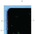
이에 따르는 종래 기술의 반증으로, 도 1에 도시된 바와 같이, 근적외선 필터(8)는 유리 기판으로부터 개별 셀 영역의 분리시 개별 셀 영역(2) 상에서 광 기능 세분층(4)의 가장자리에 뜯김 자국(6)을 갖는다. 상기 광 기능 세분층(4)의 뜯김 자국(6)은 광 기능 세분층(4)의 가장 자리에서 가시 광선과 근적외선의 광학적 조절 기능을 상실시켜 광 기능 세분층(4)의 중앙 영역에도 광학적 악 영향을 주어 광 기능 세분층(4)의 광학적 특성을 전체적으로 열악하게 하며 미세 이물이나 크랙의 발생 원인으로 작용한다.1, the near-
본 발명은, 종래의 문제점을 해결하기 위해 안출된 것으로, 강화된 유리 기판을 일정한 피치로 천공시켜 강화된 유리 기판에 복수의 필터 지지 안착체를 형성하고 강화된 유리 기판에 복수의 필터 지지 안착체를 걸친 채로 강화된 유리 기판 상에 광 필터층을 증착한 후, 강화된 유리 기판으로부터 복수의 필터 지지 안착체를 분리시, 개별 필터 지지 안착체 상에서 광 필터 세분층의 가장 자리에 뜯김 자국을 갖지 않도록 하는데 적합한 근적외선 필터 및 그 필터의 제조방법을 제공하는데 그 목적이 있다.SUMMARY OF THE INVENTION The present invention has been conceived to solve the conventional problems, and it is an object of the present invention to provide a glass substrate having a plurality of filter support supports on a reinforced glass substrate, To separate the plurality of filter support assemblies from the reinforced glass substrate and to avoid tearing marks at the edges of the optical filter granular layer on the individual filter support assemblies after deposition of the optical filter layer on the reinforced glass substrate And a method of manufacturing the filter.
본 발명에 따른 근적외선 필터는, 사각 기둥의 셀 영역, 그리고 상기 셀 영역의 사방을 둘러싸고 상기 셀 영역으로부터 점차적으로 작아지는 형상을 갖는 더미 영역으로 이루어지는 필터 지지 안착체; 및 상기 필터 지지 안착체에서 전면에 입사하여 배면을 투과하는 광선의 경로를 기준으로 볼 때, 상기 필터 지지 안착체의 상기 전면과 상기 배면에서 상기 셀 영역과 상기 더미 영역을 덮는 광 필터 세분층을 포함하고, 상기 더미 영역은 상기 필터 지지 안착체의 상기 전면과 상기 배면 중 적어도 한 쪽에서 비스듬하게 기울어지는 챔퍼 면을 가지고, 상기 광 필터 세분층은 상기 셀 영역과 상기 더미 영역에서 근적외선을 통과(pass)시키거나 상기 근적외선을 차단(cut-off)시키고, 상기 더미 영역에서 상기 필터 지지 안착체의 외부와 접촉하는 더미 내부 투영 면 상에 매끈한 면을 가지며, 상기 매끈한 면은 상기 더미 영역의 상기 더미 내부 투명 면과 동일한 일직선 상에 위치되는 것을 특징으로 한다.A near infrared ray filter according to the present invention comprises: a filter supporting seat comprising a cell region of a quadrangular pole, and a dummy region surrounding the cell region and having a shape gradually becoming smaller from the cell region; And an optical filter sub-layer covering the cell area and the dummy area on the front surface and the back surface of the filter support mount, with reference to a path of a light ray incident on the front surface of the filter support surface and transmitted through the rear surface, Wherein the dummy region has a chamfered surface that tapers obliquely from at least one of the front surface and the back surface of the filter support seat, and wherein the optical filter sub-layer passes near infrared rays in the cell region and the dummy region ) Or cut off the near infrared rays and has a smooth surface on the dummy inner projection surface that contacts the outside of the filter support seat in the dummy area and the smooth surface is in the dummy area And is located on the same straight line as the transparent surface.
상기 필터 지지 안착체는, 소다라임 유리(sodalime glass) 또는 알루미노 실리케이트 유리(alumino silicate glass)를 포함할 수 있다.The filter support seat may include sodalime glass or alumino silicate glass.
상기 필터 지지 안착체는, 상기 광 필터 세분층 아래에서, 상기 셀 영역의 표면과 상기 더미 영역의 표면과 상기 더미 영역의 상기 더미 내부 투영 면을 따라 상기 필터 지지 안착체의 내부와 다른 종류의 원소를 갖는 강화층을 더 포함할 수 있다.Wherein the filter support seat has, under the optical filter sub-layer, a surface of the cell region, a surface of the dummy region, and an interior of the filter support seat along the dummy inner projection surface of the dummy region, The reinforcing layer having a thickness of less than about < RTI ID = 0.0 >
상기 필터 지지 안착체는, 질산칼륨(KNO3)을 포함하는 용탕조에서, 상기 필터 지지 안착체의 알칼리 이온(Na+)과 질산칼륨(KNO3)의 알칼리 이온(K+)의 상호 확산을 통해 표면에 압축 응력을 가지도록 강화 처리될 수 있다.The filter support seat body is in a molten metal bath comprising potassium nitrate (KNO3), through the inter-diffusion of alkali ions (K+) of alkali ions (Na+) and potassium nitrate (KNO3) of the filter support mounting member It can be reinforced to have compressive stress on the surface.
상기 필터 지지 안착체는, 상기 더미 영역의 상기 챔퍼 면에서, 상기 셀 영역으로부터 상기 더미 내부 투영 면을 향해 비스듬하게 기울어질 수 있다.The filter support seat can be inclined at an angle from the cell area toward the dummy inner projection surface, at the chamfered surface of the dummy area.
상기 셀 영역과 상기 더미 영역은 상기 필터 지지 안착체의 상기 전면과 상기 배면 중 상기 적어도 한 쪽의 상기 챔퍼 면 주변에서 상기 셀 영역의 모서리 마다 대각선으로 마주하는 라운드된 형상을 가질 수 있다.The cell region and the dummy region may have a rounded shape that diagonally faces each corner of the cell region at the periphery of the chamfer surface of the at least one of the front surface and the back surface of the filter support seat.
상기 더미 내부 투영 면의 길이는, 상기 광선의 상기 경로를 기준으로 볼 때, 상기 광 필터 세분층의 두께보다 더 큰 크기를 가질 수 있다.The length of the dummy internal projection surface may be larger than the thickness of the optical filter sub-layer when viewed from the path of the light beam.
상기 광 필터 세분층은, 상기 필터 지지 안착체의 상기 전면과 상기 배면 중 하나의 면에서 작은 적층 횟수를 가지고, 상기 필터 지지 안착체의 상기 전면과 상기 배면에서 적층 물질로 이루어질 수 있다.The optical filter fine layer may have a small number of times of lamination on one of the front surface and the rear surface of the filter supporting seat and may be formed of a laminated material on the front surface and the rear surface of the filter supporting seat.
상기 광 필터 세분층은, 상기 적층 물질로써, 교대로 그리고 반복적으로 적층되는 이산화 규소(SiO2)와 산화티탄늄(TiO2 또는 Ti3O5) 또는 이산화 규소(SiO2)와 산화탄탈륨(Ta2O5) 또는 이산화 규소(SiO2)와 오산화니오븀(Nb2O5)을 포함할 수 있다.The optical filter sub-layer may be formed of a material selected from the group consisting of silicon dioxide (SiO2 ), titanium oxide (TiO2 or Ti3 O5 ) or silicon dioxide (SiO2 ) and tantalum oxide (Ta2 O5 ) or silicon dioxide (SiO2 ) and niobium pentoxide (Nb2 O5 ).
상기 광 필터 세분층은, 상기 필터 지지 안착체의 상기 하나의 면에서 교대로 그리고 반복적으로 이산화 규소(SiO2)와 산화티탄늄(TiO2 또는 Ti3O5) 또는 이산화 규소(SiO2)와 산화탄탈륨(Ta2O5) 또는 이산화 규소(SiO2)와 오산화니오븀(Nb2O5)을 적층시켜 이루어지고, 상기 필터 지지 안착체의 상기 하나의 면 상에 위치되는 상기 적층 물질을 동일하게 가지거나 상기 적층 물질과 다르게 가지도록, 상기 필터 지지 안착체의 상기 나머지 면에서 교대로 그리고 반복적으로 이산화 규소(SiO2)와 산화티탄늄(TiO2 또는 Ti3O5) 또는 이산화 규소(SiO2)와 산화탄탈륨(Ta2O5) 또는 이산화 규소(SiO2)와 오산화니오븀(Nb2O5)을 적층시켜 이루어질 수 있다.The optical filter sub-layer may be formed by alternating and repeatedly depositing silicon dioxide (SiO2 ) and titanium oxide (TiO2 or Ti3 O5 ) or silicon dioxide (SiO2 ) on the one surface of the filter support The laminated material which is formed by laminating tantalum oxide (Ta2 O5 ) or silicon dioxide (SiO2 ) and niobium pentoxide (Nb2 O5 ) on the one surface of the filter supporting seat have or to have different from the laminate material, wherein the filter support alternately at the second side of the seat body and repeatedly silicon dioxide (SiO2) and titanium (TiO2 or Ti3 O5) or silicon dioxide oxide (SiO2 ), Tantalum oxide (Ta2 O5 ), silicon dioxide (SiO2 ) and niobium pentoxide (Nb2 O5 ).
상기 광 필터 세분층은, 상기 필터 지지 안착체의 상기 전면과 상기 배면 중 하나의 면에서 작은 두께를 가지고, 상기 필터 지지 안착체의 나머지 면에서 다른 물질로 이루어질 수 있다.The optical filter sub-layer may have a small thickness on one of the front and back surfaces of the filter support seat and may be made of another material on the other side of the filter support seat.
상기 광 필터 세분층은, 상기 필터 지지 안착체의 상기 하나의 면에 수지층; 및 상기 수지층 상에 그리고 상기 필터 지지 안착체의 상기 나머지 면에, 교대로 그리고 반복적으로 적층되는 이산화 규소(SiO2)와 산화티탄늄(TiO2 또는 Ti3O5) 또는 이산화 규소(SiO2)와 산화탄탈륨(Ta2O5) 또는 이산화 규소(SiO2)와 오산화니오븀(Nb2O5)을 포함하고, 상기 수지층은 우레탄 및 아크릴을 포함하는 고분자수지에 근적외선 흡수 색소를 포함할 수 있다.Wherein the optical filter sub-layer comprises: a resin layer on the one surface of the filter support seat; And the resin layer on, and the filter support mounting member of the second side, are alternately and silicon dioxide being repeatedly stacked in the (SiO2) and titanium oxide titanium (TiO2 or Ti3 O5) or silicon dioxide (SiO2 ), Tantalum oxide (Ta2 O5 ) or silicon dioxide (SiO2 ) and niobium pentoxide (Nb2 O5 ), and the resin layer may contain a near infrared absorbing dye in a polymer resin containing urethane and acrylic have.
상기 광 필터 세분층은, 상기 수지층 상에서 교대로 그리고 반복적으로 이산화 규소(SiO2)와 산화티탄늄(TiO2 또는 Ti3O5) 또는 이산화 규소(SiO2)와 산화탄탈륨(Ta2O5) 또는 이산화 규소(SiO2)와 오산화니오븀(Nb2O5)을 적층시켜 이루어지고, 상기 수지층 상에서 보다 더 작은 두께를 가지면서 상기 수지층 상에 위치되는 적층물질을 동일하게 가지도록, 상기 필터 지지 안착체의 상기 나머지 면에서 교대로 그리고 반복적으로 이산화 규소(SiO2)와 산화티탄늄(TiO2 또는 Ti3O5) 또는 이산화 규소(SiO2)와 산화탄탈륨(Ta2O5) 또는 이산화 규소(SiO2)와 오산화니오븀(Nb2O5)을 적층시켜 이루어질 수 있다.The optical filter three minutes layer, alternately on the resin layer and repeatedly silicon dioxide (SiO2) and titanium oxide titanium (TiO2 or Ti3 O5) or silicon dioxide (SiO2) and tantalum (Ta2 O5 oxide ) Or silicon dioxide (SiO2 ) and niobium pentoxide (Nb2 O5 ), and has a thickness smaller than that on the resin layer and has the same laminate material positioned on the resin layer (SiO2 ) and titanium oxide (TiO2 or Ti3 O5 ) or silicon dioxide (SiO2 ) and tantalum oxide (Ta2 O5 ) or alternately and repeatedly in the remaining surface of the filter support- (SiO2 ) and niobium pentoxide (Nb2 O5 ).
상기 광 필터 세분층은 상기 필터 지지 안착체의 외부에 상기 더미 영역의 상기 더미 내부 투영 면을 노출시킬 수 있다.The optical filter sub-layer may expose the dummy interior projection surface of the dummy area outside the filter support seat.
삭제delete
본 발명에 따르는 근적외선 필터의 제조방법은, 유리 기판을 준비하는 제1 단계; 상기 유리 기판의 전면과 배면 상에 2차원 배열의 복수의 포토레지스트 패턴을 형성하는 제2 단계; 상기 유리 기판에 개별 포토레지스트 패턴 주변에서 복수의 균열 발생 기공을 천공하여 상기 유리 기판의 상기 전면과 상기 배면 중 적어도 한 쪽에서 상기 개별 포토레지스트 패턴 주변에 더미 예정 영역을 한정하는 필터 예정 받침대를 형성하는 제3 단계; 상기 천공된 유리 기판에서 상기 복수의 균열 발생 기공과 함께 상기 더미 예정 영역에 습식 식각 공정을 수행하여 상기 더미 예정 영역을 더미 한정 영역으로 변경하면서 상기 더미 한정 영역에 챔퍼 면을 형성하는 제4 단계; 상기 식각된 유리 기판으로부터 상기 복수의 포토레지스트 패턴을 제거하여 상기 복수의 식각된 균열 발생 기공에 의해 한정되는 필터 지지 중간물을 형성하는 제5 단계; 상기 식각된 유리 기판에 화학 강화 공정을 수행하여 상기 필터 지지 중간물을 필터 지지 안착체로 변경시키는 제6 단계; 및 상기 강화된 유리 기판을 덮어 상기 필터 지지 안착체에 근적외선을 통과(pass)시키거나 상기 필터 지지 안착체에 대해 상기 근적외선을 차단(cut-off)시키는 광 필터층을 형성하는 제7 단계를 수행하는 것을 포함한다.A method of manufacturing a near-infrared light filter according to the present invention includes: a first step of preparing a glass substrate; A second step of forming a plurality of photoresist patterns in a two-dimensional array on the front and back surfaces of the glass substrate; A plurality of crack generating pores are perforated around the individual photoresist patterns on the glass substrate so as to form a filter scheduled pedestal which defines a predetermined dummy area around the individual photoresist patterns on at least one of the front surface and the back surface of the glass substrate A third step; A fourth step of performing a wet etching process on the dummy predetermined region together with the plurality of crack generating pores in the perforated glass substrate to form a chamfered surface in the dummy limited region while changing the dummy predetermined region to a dummy limited region; A fifth step of removing the plurality of photoresist patterns from the etched glass substrate to form a filter support intermediate defined by the plurality of etched crack generating pores; A sixth step of performing a chemical strengthening process on the etched glass substrate to change the filter supporting intermediate to a filter supporting member; And a seventh step of forming an optical filter layer covering the reinforced glass substrate to pass near infrared rays to the filter support seat or to cut off the near infrared rays to the filter support seat .
상기 유리 기판에 상기 복수의 균열 발생 기공을 천공하는 것은, 상기 유리 기판에 레이저 빔의 빔 스팟(beam spot)을 반복적으로 조사하여 하나의 빔 스팟에 개별 균열 발생 기공을 대응시키고, 상기 레이저 빔의 조사 동안 상기 개별 포토레지스트 패턴의 둘레를 따라 상기 복수의 균열 발생 기공 사이에 균열을 야기시키는 것을 포함할 수 있다.The step of puncturing the plurality of crack generating pores on the glass substrate may include repeatedly irradiating the glass substrate with a beam spot of the laser beam to correspond individual crack generating pores to one beam spot, And causing cracks between the plurality of crack generating pores along the periphery of the individual photoresist patterns during irradiation.
상기 필터 예정 받침대는, 상기 천공된 유리 기판에서, 상기 개별 포토레지스트 패턴의 점유 영역과 함께 상기 더미 예정 영역을 포함할 수 있다.The filter scheduled pedestal may include the dummy predeterminate region with the occupied area of the individual photoresist pattern in the perforated glass substrate.
상기 천공된 유리 기판에 상기 습식 식각 공정을 수행하는 것은, 25℃? 내지 30℃?로 유지되어 불산(HF)을 포함하는 습식 식각조에 상기 천공된 유리 기판을 침지시키고, 상기 개별 포토레지스트 패턴을 식각 마스크로 사용하여, 상기 천공된 유리 기판에서 상기 복수의 균열 발생 기공에 상기 불산을 침투시키고, 상기 불산을 사용하여 상기 복수의 균열 발생 기공과 함께 상기 복수의 균열 발생 기공 사이의 균열을 통해 상기 더미 예정 영역의 선택적인 식각으로 상기 더미 한정 영역을 형성하는 것을 포함할 수 있다.The wet etching process is performed on the perforated glass substrate at 25 ° C? To 30 占 폚, so as to immerse the perforated glass substrate in a wet etching bath containing hydrofluoric acid (HF), and using the individual photoresist pattern as an etching mask, the plurality of crack generating pores And forming the dummy confinement region by selective etching of the dummy predetermined region through cracks between the plurality of crack generating pores together with the plurality of crack generating pores using the hydrofluoric acid .
상기 챔퍼 면은, 상기 개별 포토레지스트 패턴의 측벽으로부터 복수의 식각된 균열 발생 기공을 향해 점차적으로 낮아져 비스듬하게 기울어지도록, 직각 삼각형으로 이루어진 단면 구도에서 볼 때, 상기 면을 상기 직각 삼각형의 밑면에 투영시 상기 개별 포토레지스트 패턴의 측벽을 기준으로 하여 50㎛ 내지 200㎛의 수평 길이를 가지고, 상기 면을 상기 직각 삼각형의 높이에 투영시 상기 개별 포토레지스트 패턴의 바닥을 기준으로 하여 2㎛ 내지 10㎛ 의 수직 길이를 가질 수 있다.Wherein the chamfered surface is projected on the underside of the right triangle in a cross-sectional view of a right triangle so that the chamfered surface is inclined obliquely from the side walls of the individual photoresist pattern toward the plurality of etched crack generating pores. Wherein the photoresist pattern has a horizontal length of 50 mu m to 200 mu m with respect to the side wall of the individual photoresist pattern, and when the surface is projected on the height of the right triangle, 2 mu m to 10 mu m Lt; / RTI >
상기 필터 지지 중간물은, 상기 식각된 유리 기판에서, 상기 더미 한정 영역과 상기 더미 한정 영역으로 둘러싸인 예비 셀 영역을 포함할 수 있다.The filter support intermediate may include, in the etched glass substrate, a spare cell region surrounded by the dummy confinement region and the dummy confinement region.
상기 식각된 유리 기판에 화학 강화 공정을 수행하는 것은, 350℃? 내지 450℃?로 유지되어 질산 칼륨(KNO3)을 포함하는 용탕조에 상기 식각된 유리 기판을 침지시키고, 상기 용탕조에서 상기 질산 칼륨(KNO3)과 상기 식각된 유리 기판의 화학 반응 동안 상기 식각된 유리 기판의 알칼리 이온(Na+)과 상기 질산칼륨(KNO3)의 알칼리 이온(K+)을 상호 확산시켜 상기 식각된 유리 기판의 표면에 알칼리 이온(K+)을 침투시키고, 상기 식각된 유리 기판을 냉각시켜 상기 식각된 유리 기판의 표면에 압축 응력을 가지도록 상기 식각된 유리 기판의 상기 표면에 강화층을 형성하는 것을 포함할 수 있다.To perform the chemical strengthening process on the etched glass substrate, (KNO 3) and the etched glass substrate during the chemical reaction of the etched glass substrate with the potassium nitrate (KNO 3) in the molten bath, Alkali ions (K+ ) penetrate the surface of the etched glass substrate by interdiffusion of alkaline ions (Na+ ) of the substrate and alkali ions (K+ ) of the potassium nitrate (KNO3 ) And forming an enhancement layer on the etched surface of the glass substrate so as to have compressive stress on the surface of the etched glass substrate.
상기 필터 지지 안착체는, 상기 화학 강화 공정의 수행 동안, 상기 필터 지지 중간물에서 상기 더미 한정 영역과 상기 예비 셀 영역의 표면에 강화층을 포함시켜 상기 더미 한정 영역과 상기 예비 셀 영역을 상기 더미 영역과 상기 셀 영역으로 변경하여 형성될 수 있다.Wherein the filter support seat includes an enhancement layer on the surface of the dummy confinement region and the preliminary cell region in the filter support intermediate during the performance of the chemical reinforcement process to form the dummy confinement region and the preliminary cell region in the dummy confinement region, Region and the cell region.
상기 광 필터층은, 상기 강화된 유리 기판의 전면과 배면 중 하나의 면 상에 교대로 그리고 반복적으로 이산화 규소(SiO2)와 산화티탄늄(TiO2 또는 Ti3O5) 또는 이산화 규소(SiO2)와 산화탄탈륨(Ta2O5) 또는 이산화 규소(SiO2)와 오산화니오븀(Nb2O5)을 적층시키고, 상기 강화된 유리 기판의 상기 하나의 면 보다 작은 적층 횟수를 가지면서 동일하거나 다른 적층 물질을 가지도록, 상기 강화된 유리 기판의 나머지 면 상에 교대로 그리고 반복적으로 이산화 규소(SiO2)와 산화티탄늄(TiO2 또는 Ti3O5) 또는 이산화 규소(SiO2)와 산화탄탈륨(Ta2O5) 또는 이산화 규소(SiO2)와 오산화니오븀(Nb2O5)을 적층시켜 형성될 수 있다.The optical filter layer may be formed by alternately and repeatedly depositing silicon dioxide (SiO2 ) and titanium oxide (TiO2 or Ti3 O5 ) or silicon dioxide (SiO2 ) on one of the front and back surfaces of the reinforced glass substrate ) and tantalum oxide (Ta2 O5) or silicon dioxide (SiO2) and phosphorus pentoxide and niobium (Nb2 O5) a stack and, wherein the hardened glass substrate having a more equal while having a small lamination number, or the other side of the so as to have a layered material, alternately on the second side of said glass substrate and repeatedly silicon dioxide (SiO2) and titanium oxide titanium (TiO2 or Ti3 O5) or silicon dioxide (SiO2) and tantalum oxide (Ta2 O5 ) or silicon dioxide (SiO2 ) and niobium pentoxide (Nb2 O5 ).
상기 광 필터층은, 상기 강화된 유리 기판의 전면과 배면 중 하나의 면 상에 수지층; 상기 수지층 상에, 교대로 그리고 반복적으로 적층되는 이산화 규소(SiO2)와 산화티탄늄(TiO2 또는 Ti3O5) 또는 이산화 규소(SiO2)와 산화탄탈륨(Ta2O5) 또는 이산화 규소(SiO2)와 오산화니오븀(Nb2O5); 및 상기 수지층 상에서 보다 더 작은 두께를 가지면서 상기 수지층 상에 위치되는 적층물질을 동일하게 가지도록, 상기 강화된 유리 기판의 나머지 면 상에, 교대로 그리고 반복적으로 적층되는 이산화 규소(SiO2)와 산화티탄늄(TiO2 또는 Ti3O5) 또는 이산화 규소(SiO2)와 산화탄탈륨(Ta2O5) 또는 이산화 규소(SiO2)와 오산화니오븀(Nb2O5)으로 형성되고, 상기 수지층은 우레탄 및 아크릴을 포함하는 고분자수지에 근적외선 흡수 색소를 포함할 수 있다.Wherein the optical filter layer comprises: a resin layer on one of a front surface and a back surface of the reinforced glass substrate; (SiO2 ) and titanium oxide (TiO2 or Ti3 O5 ) or silicon dioxide (SiO2 ) and tantalum oxide (Ta2 O5 ) or dioctic oxide (SiO2 ) which are alternately and repeatedly stacked on the resin layer. Silicon (SiO2 ) and niobium pentoxide (Nb2 O5 ); And while having a smaller thickness than over the resin layer on a surface of the remainder of said glass substrate so that the same kinds of the laminated material that is formed on the resin layer, are alternately and repeatedly silicon dioxide (SiO2 stacked in the (TiO2 or Ti3 O5 ) or silicon dioxide (SiO2 ), tantalum oxide (Ta2 O5 ) or silicon dioxide (SiO2 ) and niobium pentoxide (Nb2 O5 ) The resin layer may include a near infrared absorbing dye in a polymer resin containing urethane and acrylic.
상기 근적외선 필터의 제조방법은, 상기 제5 단계와 상기 제6 단계 사이에 또는 상기 제6 단계와 상기 제7 단계 사이에 습식 처리 단계를 수행하는 것을 더 포함하고, 상기 습식 처리 단계는 상기 제5 단계와 상기 제6 단계 사이에서 비불산 또는 불산을 포함하는 습식 식각액을 상기 식각된 유리 기판에 적용하여 상기 식각된 유리 기판의 표면을 부분적으로 식각하거나, 상기 제6 단계와 상기 제7 단계 사이에서 상기 비불산 또는 불산을 포함하는 습식 식각액을 상기 강화된 유리 기판에 적용하여 상기 강화된 유리 기판의 표면을 부분적으로 식각할 수 있다.The method of manufacturing a near-infrared ray filter according to claim 1, further comprising performing a wet processing step between the fifth step and the sixth step or between the sixth step and the seventh step, Between the sixth step and the sixth step, a wet etchant containing a non-hydrofluoric acid or a hydrofluoric acid is applied to the etched glass substrate to partially etch the surface of the etched glass substrate, or between the sixth step and the seventh step A wet etchant containing the non-hydrofluoric acid or hydrofluoric acid may be applied to the reinforced glass substrate to partially etch the surface of the reinforced glass substrate.
상기 근적외선 필터의 제조방법은, 상기 제7 단계를 수행한 후, 상기 강화된 유리 기판으로부터 상기 복수의 식각된 균열 발생 기공을 따라 상기 복수의 필터 지지 안착체를 분리하면서, 상기 복수의 식각된 균열 발생 기공을 균열 전사체로 이용하여 상기 복수의 필터 지지 안착체 상에서 상기 광 필터층을 세분해서 상기 개별 필터 지지 안착체 상에 광 필터 세분층을 형성하는 제8 단계를 수행하는 것을 더 포함할 수 있다.The manufacturing method of the near-infrared ray filter may further include, after performing the seventh step, separating the plurality of filter supporting seams from the reinforced glass substrate along the plurality of etched crack generating pores, And performing an eighth step of forming an optical filter sub-layer on the individual filter supporting member by using the generated pores as a crack transfer member to subdivide the optical filter sub-layer on the plurality of filter supporting sub-assemblies.
본 발명에 따르면, 강화된 유리 기판을 일정한 피치로 천공시켜 강화된 유리 기판에 걸쳐진 복수의 필터 지지 안착체 상에 광 필터층을 적층시킨 상태에서 볼 때, 개별 필터 지지 안착체에 사각 기둥의 셀 영역과 셀 영역의 사방을 둘러싸는 더미 영역을 가지고, 개별 필터 지지 안착체의 전면과 배면에서 더미 영역에 서로에 대해 기울어지는 챔퍼 면을 가지므로,According to the present invention, when the reinforced glass substrate is perforated at a constant pitch and the optical filter layer is laminated on the plurality of filter support substrates laid over the reinforced glass substrate, And a dummy area enclosing all sides of the cell area and having chamfered surfaces that are inclined relative to each other in the dummy area on the front surface and the back surface of the individual filter supporting seat,
본 발명은, 강화된 유리 기판으로부터 복수의 필터 지지 안착체의 분리시, 광 필터층을 세분하기 위해 개별 필터 지지 안착체 주변에 위치되는 복수의 균열 발생 기공을 균열 전사체로 이용하여 형성되고, 개별 필터 지지 안착체 상에서 개별 필터 지지 안착체의 전면과 배면의 면적과 동일한 크기를 가지며 가장 자리에서 뜯김 자국이 없는 광 필터 세분층을 가질 수 있다.The present invention relates to a method for separating a plurality of filter support deposits from an enhanced glass substrate using a plurality of crack generating pores located around individual filter support deposits to subdivide the optical filter layer, It may have an optical filter sub-layer having a size equal to the area of the front and back surfaces of the individual filter support body on the support body and free of tear marks at the edges.
도 1은 종래 기술에 따른 근적외선 필터를 보여주는 이미지이다.
도 2는 본 발명에 따른 근적외선 필터를 보여주는 평면도이다.
도 3은 도 2의 절단선 Ⅰ - Ⅰ' 를 따라 취해 근적외선 필터를 보여주는 부분 단면도이다.
도 4는 도 2의 화살표 'Ⅱ' 방향에서 볼 때 근적외선 필터를 보여주는 측면도이다.
도 5는 도 2의 지시 영역 'A' 에서 근적외선 필터를 평면적으로 보여주는 이미지이다.
도 6 내지 도 17은 도 1의 근적외선 필터의 제조방법을 설명하는 개략도이다.1 is an image showing a near infrared ray filter according to the prior art.
2 is a plan view showing a near-infrared filter according to the present invention.
3 is a partial cross-sectional view of the near-infrared filter taken along the section line I-I 'of FIG.
FIG. 4 is a side view showing a near-infrared filter in the direction of arrow II in FIG. 2. FIG.
FIG. 5 is an image showing a near-infrared filter in a plan view in the indicating area 'A' in FIG.
Figs. 6 to 17 are schematic views for explaining a manufacturing method of the near-infrared ray filter of Fig.
후술하는 본 발명에 대한 상세한 설명은, 본 발명이 실시될 수 있는 특정 실시 예를 예시로서 도시하는 첨부 도면을 참조한다. 이들 실시 예는 당업자가 본 발명을 실시할 수 있기에 충분하도록 상세히 설명된다. 본 발명의 다양한 실시 예는 서로 다르지만 상호 배타적일 필요는 없음이 이해되어야 한다. 예를 들어, 여기에 기재되어 있는 특정 형상, 구조 및 특성은 일 실시 예에 관련하여 본 발명의 정신 및 범위를 벗어나지 않으면서 다른 실시 예로 구현될 수 있다. 또한, 각각의 개시된 실시예 내의 개별 구성요소의 위치 또는 배치는 본 발명의 정신 및 범위를 벗어나지 않으면서 변경될 수 있음이 이해되어야 한다. 따라서, 후술하는 상세한 설명은 한정적인 의미로서 취하려는 것이 아니며, 본 발명의 범위는, 적절하게 설명된다면, 그 청구항들이 주장하는 것과 균등한 모든 범위와 더불어 첨부된 청구항에 의해서만 한정된다. 도면에서 유사한 참조부호는 여러 측면에 걸쳐서 동일하거나 유사한 기능을 지칭하며, 길이 및 면적, 두께 등과 그 형태는 편의를 위하여 과장되어 표현될 수도 있다.The following detailed description of the invention refers to the accompanying drawings, which illustrate, by way of illustration, specific embodiments in which the invention may be practiced. These embodiments are described in sufficient detail to enable those skilled in the art to practice the invention. It should be understood that the various embodiments of the present invention are different, but need not be mutually exclusive. For example, certain features, structures, and characteristics described herein may be implemented in other embodiments without departing from the spirit and scope of the invention in connection with one embodiment. It is also to be understood that the position or arrangement of the individual components within each disclosed embodiment may be varied without departing from the spirit and scope of the invention. The following detailed description is, therefore, not to be taken in a limiting sense, and the scope of the present invention is to be limited only by the appended claims, along with the full scope of equivalents to which such claims are entitled, if properly explained. In the drawings, like reference numerals refer to the same or similar functions throughout the several views, and length and area, thickness, and the like may be exaggerated for convenience.
이하에서는, 본 발명이 속하는 기술분야에서 통상의 지식을 가진 자가 본 발명을 용이하게 실시할 수 있도록 하기 위하여, 본 발명의 바람직한 실시 예(들)에 관하여 첨부된 도면을 참조하여 상세히 설명하기로 한다.Hereinafter, preferred embodiments (s) of the present invention will be described in detail with reference to the accompanying drawings so that those skilled in the art can easily carry out the present invention .
도 2는 본 발명에 따른 근적외선 필터를 보여주는 평면도이고, 도 3은 도 2의 절단선 Ⅰ - Ⅰ' 를 따라 취해 근적외선 필터를 보여주는 부분 단면도이다.FIG. 2 is a plan view showing a near-infrared filter according to the present invention, and FIG. 3 is a partial cross-sectional view showing a near-infrared filter taken along a cutting line I-I 'of FIG.
또한, 도 4는 도 2의 화살표 'Ⅱ' 방향에서 볼 때 근적외선 필터를 보여주는 측면도이고, 도 5는 도 2의 지시 영역 'A' 에서 근적외선 필터를 평면적으로 보여주는 이미지이다.FIG. 4 is a side view showing the near-infrared filter in the direction of arrow 'II' in FIG. 2, and FIG. 5 is an image showing the near-infrared filter in a plan view in the indicating area 'A' in FIG.
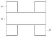
도 2 내지 도 5를 참조하면, 본 발명에 따른 근적외선 필터(110)는, 필터 지지 안착체(95)와 광 필터 세분층(105)을 도 2 내지 도 4와 같이 포함한다. 상기 필터 지지 안착체(95)는, 소다라임 유리(sodalime glass) 또는 알루미노 실리케이트 유리(alumino silicate glass)를 포함한다. 상기 필터 지지 안착체(95)는, 사각 기둥의 셀 영역(90), 그리고 셀 영역(90)의 사방을 둘러싸고 셀 영역(90)으로부터 점차적으로 작아지는 형상을 갖는 더미 영역(18)을 포함한다.2 to 5, the near
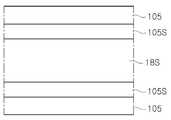
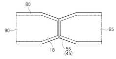
또한, 상기 필터 지지 안착체(95)는, 도 3과 같이, 광 필터 세분층(105) 아래에서, 셀 영역(90)의 표면과 더미 영역(18)의 표면을 따라 필터 지지 안착체(95)의 내부와 다른 종류의 원소를 갖는 강화층(80)을 더 포함한다. 좀 더 상세하게는, 상기 필터 지지 안착체(95)는, 질산칼륨(KNO3)을 포함하는 용탕조(도면에 미 도시)에서, 필터 지지 안착체(95)의 알칼리 이온(Na+)과 질산칼륨(KNO3)의 알칼리 이온(K+)의 상호 확산을 통해 표면에 압축 응력을 가지도록 강화 처리된다.3, the
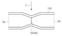
상기 필터 지지 안착체(95)는, 도 3(a) 및 도 3(b)와 같이, 더미 영역(18)의 챔퍼 면(60)에서, 셀 영역(90)으로부터 더미 내부 투영 면(18S)을 향해 비스듬하게 기울어진다. 좀 더 상세하게는, 상기 필터 지지 안착체(95)에서 전면에 입사하여 배면을 투과하는 광선의 경로를 기준으로 볼 때, 상기 더미 영역(18)의 챔퍼면(60)은 필터 지지 안착체(95)의 전면과 배면 중 적어도 한 쪽에서 비스듬하게 기울어진다.The
즉, 상기 더미 영역(18)의 챔퍼 면(60)은, 도 3(a)에서 필터 지지 안착체(95)의 전면 및 배면에 위치되고, 도 3(b)에서, 필터 지지 안착체(95)의 전면에만 위치된다. 여기서, 상기 챔퍼면(60)은, 도 3(b)와 다르게, 필터 지지 안착체(95)의 전면이 아닌 배면에만 위치될 수도 있다.3 (b), the chamfered
상기 셀 영역(90)과 더미 영역(18)은 필터 지지 안착체(95)의 전면과 배면 중 적어도 한 쪽에서 셀 영역(90)의 모서리 마다 대각선으로 마주하는 라운드된 형상을 도 1과 같이 갖는다. 상기 더미 내부 투영 면(18S)의 길이(L)는, 도 3과 같이, 광선의 경로를 기준으로 볼 때, 광 필터 세분층(105)의 두께(T)보다 더 큰 크기를 갖는다.The
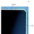
한편, 상기 광 필터 세분층(105)은, 필터 지지 안착체(95)의 전면과 배면에서 셀 영역(90)과 더미 영역(18)을 도 3 및 도 4와 같이 덮는다. 상기 광 필터 세분층(105)은, 셀 영역(90)과 더미 영역(18)에서 근적외선을 통과(pass)시키거나 근적외선을 차단(cut-off)시키고, 더미 영역(18)에서 필터 지지 안착체(95)의 외부와 접촉하는 더미 내부 투영 면(18S) 상에 매끈한 면(105S)을 도 3과 같이 갖는다.3 and 4, the optical filter
상기 광 필터 세분층(105)의 매끈한 면(105S)은, 도 5에 도시된 바와 같이, 광 필터 세분층(105)의 가장 자리에 도 1의 뜯김 자국(6)을 갖지 않게 한다. 본 발명의 일 실시예로써, 상기 광 필터 세분층(105)은, 필터 지지 안착체(95)와 함께 근적외선 패스(pass) 필터를 구현하기 위해, 필터 지지 안착체(95)의 전면과 배면 중 하나의 면에서 작은 적층 횟수를 가지고, 필터 지지 안착체(95)의 전면과 배면에서 적층 물질로 이루어진다.The
여기서, 상기 광 필터 세분층(105)은, 적층 물질로써, 교대로 그리고 반복적으로 적층되는 이산화 규소(SiO2)와 산화티탄늄(TiO2 또는 Ti3O5) 또는 이산화 규소(SiO2)와 산화탄탈륨(Ta2O5) 또는 이산화 규소(SiO2)와 오산화니오븀(Nb2O5)을 포함한다. 좀 더 상세하게는, 상기 광 필터 세분층(105)은, 필터 지지 안착체(95)의 하나의 면에서 교대로 그리고 반복적으로 이산화 규소(SiO2)와 산화티탄늄(TiO2 또는 Ti3O5) 또는 이산화 규소(SiO2)와 산화탄탈륨(Ta2O5) 또는 이산화 규소(SiO2)와 오산화니오븀(Nb2O5)을 적층시켜 이루어지고, 상기 필터 지지 안착체의 상기 하나의 면 상에 위치되는 적층 물질을 동일하게 가지거나 적층 물질과 다르게 가지도록, 필터 지지 안착체(95)의 나머지 면에서 교대로 그리고 반복적으로 이산화 규소(SiO2)와 산화티탄늄(TiO2 또는 Ti3O5) 또는 이산화 규소(SiO2)와 산화탄탈륨(Ta2O5) 또는 이산화 규소(SiO2)와 오산화니오븀(Nb2O5)을 적층시켜 이루어진다.Here, the optical filter
이와 유사하게, 본 발명의 다른 실시예로써, 상기 광 필터 세분층(105)은, 필터 지지 안착체(95)와 함께 근적외선 컷오프(cut off) 필터를 구현하기 위해, 필터 지지 안착체(95)의 전면과 배면 중 하나의 면에서 작은 두께를 가지고, 필터 지지 안착체(95)의 나머지 면에서 다른 물질로 이루어질 수 있다. 여기서, 상기 광 필터 세분층(105)은, 필터 지지 안착체(95)의 하나의 면에 수지층; 및 수지층 상에 그리고 필터 지지 안착체(95)의 나머지 면에, 교대로 그리고 반복적으로 적층되는 이산화 규소(SiO2)와 산화티탄늄(TiO2 또는 Ti3O5) 또는 이산화 규소(SiO2)와 산화탄탈륨(Ta2O5) 또는 이산화 규소(SiO2)와 오산화니오븀(Nb2O5)을 포함한다.Similarly, in another embodiment of the present invention, the
상기 수지층은 우레탄 및 아크릴을 포함하는 고분자수지에 근적외선 흡수 색소를 포함한다. 좀 더 상세하게는, 상기 광 필터 세분층(105)은, 수지층 상에서 교대로 그리고 반복적으로 이산화 규소(SiO2)와 산화티탄늄(TiO2 또는 Ti3O5) 또는 이산화 규소(SiO2)와 산화탄탈륨(Ta2O5) 또는 이산화 규소(SiO2)와 오산화니오븀(Nb2O5)을 적층시켜 이루어지고, 상기 수지층 상에서 보다 더 작은 두께를 가지면서 상기 수지층 상에 위치되는 적층물질을 동일하게 가지도록, 필터 지지 안착체(95)의 나머지 면에서 교대로 그리고 반복적으로 이산화 규소(SiO2)와 산화티탄늄(TiO2 또는 Ti3O5) 또는 이산화 규소(SiO2)와 산화탄탈륨(Ta2O5) 또는 이산화 규소(SiO2)와 오산화니오븀(Nb2O5)을 적층시켜 이루어진다.The resin layer includes a near infrared absorbing dye in a polymer resin containing urethane and acryl. More specifically, the
상기 광 필터 세분층(105)은 필터 지지 안착체(95)의 외부에 더미 영역(18)의 더미 내부 투영 면(18S)을 도 3(a), 도 3(b) 및 도 4와 같이 노출시킨다. 상기 광 필터 세분층(105)의 매끈한 면(105S)은 더미 영역(18)의 더미 내부 투영 면(18S)과 동일한 일직선 상에 도 3 및 도 5와 같이 위치된다.The optical
다음으로, 본 발명에 따른 근적외선 필터의 제조방법은 도 6 내지 도 17을 참조하여 상세하게 설명하기로 한다.Next, a manufacturing method of the near-infrared ray filter according to the present invention will be described in detail with reference to FIG. 6 to FIG.
도 6 내지 도 17은 도 1의 근적외선 필터의 제조방법을 설명하는 개략도이다. 여기서, 도 7, 도 9, 12, 15 또는 도 17은 도 6, 도 8, 도 11, 도 14 또는 도 16의 절단선 Ⅲ - Ⅲ' 를 따라 취해 도면 별로 형성되는 구조물을 설명하는 부분 단면도이다. 또한, 도 10은 도 8의 절단선 Ⅲ - Ⅲ' 주변에서 구조물의 형상을 평면적으로 보여주는 개략도이다.Figs. 6 to 17 are schematic views for explaining a manufacturing method of the near-infrared ray filter of Fig. 7, 9, 12, 15, or 17 is a partial cross-sectional view illustrating a structure formed along the line III-III 'of FIG. 6, FIG. 11, FIG. 14, . 10 is a schematic view showing the shape of the structure in a plan view around the cutting line III-III 'in FIG.
또한, 도 6, 도 8, 도 11, 도 14 또는 도 16은 유리 기판(20), 천공된 유리 기판(23), 식각된 유리 기판(26) 또는 강화된 유리 기판(29)에서 가장자리의 변형 형상에 관심을 갖지 않아 공정 단계 별로 변형 형상을 도시하지 않는다.6, Fig. 8, Fig. 11, Fig. 14 or Fig. 16 shows the deformation of the edge in the
도 6 내지 도 17을 참조하면, 본 발명에 따르는 근적외선 필터의 제조방법은, 본 발명의 이해를 빠르게 돕기 위해 도 3(a)를 바탕으로 설명될 수 있다. 이를 위해, 본 발명에 따르는 근적외선 필터의 제조방법은, 유리 기판(20)을 준비하는 제1 단계를 도 6과 같이 수행하는 것을 포함할 수 있다.Referring to Figs. 6 to 17, a method of manufacturing a near-infrared light filter according to the present invention can be described on the basis of Fig. 3 (a) to help the understanding of the present invention. To this end, the manufacturing method of the near-infrared light filter according to the present invention may include performing the first step of preparing the
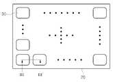
상기 유리 기판(20)은 도 1 내지 도 5의 필터 지지 안착체(95)에서 상세히 설명되었다. 계속해서, 상기 근적외선 필터의 제조방법은, 유리 기판(20)의 전면과 배면 상에 2차원 배열의 복수의 포토레지스트 패턴(30)을 형성하는 제2 단계를 도 6 및 도 7과 같이 수행하는 것을 포함할 수 있다.The
계속해서, 상기 근적외선 필터의 제조방법은, 유리 기판(20)에 개별 포토레지스트 패턴(30) 주변에서 복수의 균열 발생 기공(40)을 천공하여 개별 포토레지스트 패턴(30) 주변에 더미 예정 영역(10)을 한정하는 필터 예정 받침대(35)를 형성하는 제3 단계를 도 8 내지 도 10과 같이 수행하는 것을 포함할 수 있다.The near infrared ray filter manufacturing method is characterized in that a plurality of
좀 더 구체적으로, 상기 유리 기판(20)에 복수의 균열 발생 기공(40)을 천공하는 것은, 유리 기판(20)에 레이저 빔(도면에 미 도시)의 빔 스팟(beam spot)을 반복적으로 조사하여 하나의 빔 스팟에 개별 균열 발생 기공(40)을 대응시키고, 레이저 빔의 조사 동안 개별 포토레지스트 패턴(30)의 둘레를 따라 복수의 균열 발생 기공(40) 사이에 균열(도 10의 50)을 야기시키는 것을 포함할 수 있다.More specifically, puncturing the plurality of
상기 필터 예정 받침대(35)는, 천공된 유리 기판(23)의 전면 및 배면에서, 개별 포토레지스트 패턴(30)의 점유 영역과 함께 더미 예정 영역(10)을 포함한다. 계속해서, 상기 근적외선 필터의 제조방법은, 천공된 유리 기판(23)에서 복수의 균열 발생 기공(40)과 함께 더미 예정 영역(10)에 습식 식각 공정을 수행하여 더미 예정 영역(10)을 더미 한정 영역(14)으로 변경하면서 더미 한정 영역(14)에 챔퍼 면(60)을 형성하는 제4 단계를 도 11 및 도 12와 같이 수행하는 것을 포함할 수 있다.The filter predetermined
상기 천공된 유리 기판(23)에 습식 식각 공정을 수행하는 것은, 25℃ 내지 30℃로 유지되어 불산(HF)을 포함하는 습식 식각조에 천공된 유리 기판(23)을 침지시키고, 개별 포토레지스트 패턴(30)을 식각 마스크로 사용하여, 천공된 유리 기판(23)에서 복수의 균열 발생 기공(40)에 불산을 침투시키고, 불산을 사용하여 복수의 균열 발생 기공(40)과 함께 복수의 균열 발생 기공(40) 사이의 균열(도 10의 50)을 통해 더미 예정 영역(10)의 선택적인 식각으로 더미 한정 영역(14)을 형성하는 것을 포함한다.The wet etching process is performed on the
상기 더미 예정 영역(10)의 선택적인 식각은 식각된 유리 기판(26)에 복수의 식각된 균열 발생 기공(45)과 함께 복수의 식각된 균열 발생 기공(45) 사이에 식각된 균열(55)을 형성하도록 수행될 수 있다.The selective etching of the
상기 챔퍼 면(60)은, 개별 포토레지스트 패턴(30)의 측벽으로부터 복수의 식각된 균열 발생 기공(45)을 향해 점차적으로 낮아져 비스듬하게 기울어지도록, 도 12와 같이, 직각 삼각형으로 이루어진 단면 구도에서 볼 때, 챔퍼 면(60)을 직각 삼각형의 밑변에 투영시 개별 포토레지스트 패턴(30)의 측벽을 기준으로 하여 50㎛ 내지 200㎛의 수평 길이(W)를 가지고, 챔퍼 면(60)을 직각 삼각형의 높이에 투영시 개별 포토레지스트 패턴(30)의 바닥을 기준으로 하여 2㎛ 내지 10㎛ 의 수직 길이(D)를 갖는다.The chamfered
다음으로, 상기 근적외선 필터의 제조방법은, 식각된 유리 기판(26)으로부터 복수의 포토레지스트 패턴(30)을 제거하여 복수의 식각된 균열 발생 기공(45)에 의해 한정되는 필터 지지 중간물(75)을 형성하는 제5 단계를 도 13과 같이 수행하는 것을 포함할 수 있다. 여기서, 상기 필터 지지 중간물(75)은, 식각된 유리 기판(26)에서, 더미 한정 영역(14)과 더미 한정 영역(14)으로 둘러싸인 예비 셀 영역(70)을 포함할 수 있다. 이어서, 상기 근적외선 필터의 제조방법은, 식각된 유리 기판(26)에 화학 강화 공정을 수행하여 필터 지지 중간물(75)을 필터 지지 안착체(95)로 변경시키는 제6 단계를 도 14 및 도 15와 같이 수행하는 것을 포함할 수 있다.Next, the manufacturing method of the near-infrared ray filter is to remove the plurality of
상기 식각된 유리 기판(26)에 화학 강화 공정을 수행하는 것은, 350℃ 내지 450℃로 유지되어 질산 칼륨(KNO3)을 포함하는 용탕조에 식각된 유리 기판(26)을 침지시키고, 용탕조에서 질산 칼륨(KNO3)과 식각된 유리 기판(26)의 화학 반응 동안 식각된 유리 기판(26)의 알칼리 이온(Na+)과 질산칼륨(KNO3)의 알칼리 이온(K+)을 상호 확산시켜 식각된 유리 기판(26)의 표면에 알칼리 이온(K+)을 침투시키고, 식각된 유리 기판(26)을 냉각시켜 식각된 유리 기판(26)의 표면에 압축 응력을 가지도록 식각된 유리 기판(26)의 표면에 강화층(80)을 형성하는 것을 포함할 수 있다.The chemical strengthening process is performed on the etched
상기 필터 지지 안착체(95)는, 화학 강화 공정의 수행 동안, 필터 지지 중간물(75)에서 더미 한정 영역(14)과 예비 셀 영역(70)의 표면에 강화층(80)을 포함시켜 더미 한정 영역(14)과 예비 셀 영역(70)을 더미 영역(18)과 셀 영역(90)으로 변경하여 형성된다. 이어서, 상기 근적외선 필터의 제조방법은, 강화된 유리 기판(29)을 덮어 필터 지지 안착체(95)에 근적외선을 통과(pass)시키거나 필터 지지 안착체(95)에 대해 근적외선을 차단(cut-off)시키는 광 필터층(100)을 형성하는 제7 단계를 도 16 및 도 17과 같이 수행하는 것을 포함할 수 있다.The
상기 광 필터층(100)은, 도 1 내지 도 5에서 개시되는 근적외선 패스 필터를 형성하기 위해, 강화된 유리 기판(29)의 전면과 배면 중 하나의 면 상에 교대로 그리고 반복적으로 이산화 규소(SiO2)와 산화티탄늄(TiO2 또는 Ti3O5) 또는 이산화 규소(SiO2)와 산화탄탈륨(Ta2O5) 또는 이산화 규소(SiO2)와 오산화니오븀(Nb2O5)을 적층시키고, 상기 강화된 유리 기판의 하나의 면 보다 작은 적층 횟수를 가지면서 동일하거나 다른 적층 물질을 가지도록, 강화된 유리 기판(29)의 나머지 면 상에 교대로 그리고 반복적으로 이산화 규소(SiO2)와 산화티탄늄(TiO2 또는 Ti3O5) 또는 이산화 규소(SiO2)와 산화탄탈륨(Ta2O5) 또는 이산화 규소(SiO2)와 오산화니오븀(Nb2O5)을 적층시켜 형성될 수 있다.The
이와 유사하게, 상기 광 필터층(100)은, 도 1 내지 도 5에서 개시되는 근적외선 컷오프 필터를 형성하기 위해, 강화된 유리 기판(29)의 전면과 배면 중 하나의 면 상에 수지층; 수지층 상에, 교대로 그리고 반복적으로 적층되는 이산화 규소(SiO2)와 산화티탄늄(TiO2 또는 Ti3O5) 또는 이산화 규소(SiO2)와 산화탄탈륨(Ta2O5) 또는 이산화 규소(SiO2)와 오산화니오븀(Nb2O5); 및 상기 수지층 상에서 보다 더 작은 두께를 가지면서 상기 수지층 상에 위치되는 적층물질을 동일하게 가지도록, 강화된 유리 기판(29)의 나머지 면 상에, 교대로 그리고 반복적으로 적층되는 이산화 규소(SiO2)와 산화티탄늄(TiO2 또는 Ti3O5) 또는 이산화 규소(SiO2)와 산화탄탈륨(Ta2O5) 또는 이산화 규소(SiO2)와 오산화니오븀(Nb2O5)으로 형성될 수 있다. 상기 수지층은 우레탄 및 아크릴을 포함하는 고분자수지에 근적외선 흡수 색소를 포함할 수 있다.Similarly, the
한편, 상기 근적외선 필터의 제조방법은, 제5 단계와 제6 단계 사이에 또는 제6 단계와 제7 단계 사이에 습식 처리 단계를 수행하는 것을 더 포함할 수 있다. 상기 습식 처리 단계는, 제5 단계와 제6 단계 사이에서 비불산 또는 불산을 포함하는 습식 식각액을 식각된 유리 기판(26)에 적용하여 식각된 유리 기판(26)의 표면을 부분적으로 식각하거나, 제6 단계와 제7 단계 사이에서 비불산 또는 불산을 포함하는 습식 식각액을 강화된 유리 기판(29)에 적용하여 강화된 유리 기판(29)의 표면을 부분적으로 식각하도록 수행하는 것을 더 포함할 수 있다.Meanwhile, the manufacturing method of the near-infrared ray filter may further include performing a wet processing step between the fifth and sixth steps or between the sixth and seventh steps. The wet processing step may be performed by applying a wet etchant containing non-hydrofluoric acid or hydrofluoric acid between the fifth and sixth steps to the etched
상기 습식 처리 단계는, 근적외선 필터의 제조방법을 제1 내지 제7 단계에서 단계 별로 실시하는 동안, 유리 기판(20)의 표면으로부터 유리 기판(20)의 가공전 격자 결함을 제거하거나 천공된 유리 기판(23), 식각된 유리 기판(26) 또는 강화된 유리 기판(29)의 표면에 노출된 유리 기판(20)의 가공후 격자 결함을 제거하도록 수행될 수 있다.The wet processing step removes the lattice defects of the
이어서, 상기 근적외선 필터의 제조방법은, 제7 단계의 수행후, 강화된 유리 기판(29)과 광 필터층(100)에 외부 힘(F)을 적용하는 동안, 강화된 유리 기판(29)으로부터 복수의 식각된 균열 발생 기공(45)을 따라 복수의 필터 지지 안착체(95)를 분리하면서, 복수의 식각된 균열 발생 기공(45)을 균열 전사체로 이용하여 복수의 필터 지지 안착체(95) 상에서 광 필터층(100)을 세분해서 개별 필터 지지 안착체(95) 상에 광 필터 세분층(도 1의 105)을 형성하는 제8 단계를 수행하는 것을 더 포함할 수 있다.The method of manufacturing the near-infrared light filter further comprises a step of removing a plurality (from the reinforced glass substrate 29) from the reinforced
상기 개별 필터 지지 안착체(95)와 광 필터 세분층(105)은 도 1의 근적외선 필터(110)를 구성할 수 있다. 상기 근적외선 필터(110)는 근적외선 패스 필터 또는 근적외선 컷오프 필터일 수 있다.The individual
본 발명의 변형 예로써, 본 발명에 따르는 근적외선 필터의 제조방법은, 도 3(b)의 구조를 구현하기 위해, 상기 근적외선 필터의 제조방법은, 유리 기판(20)의 전면과 배면 상에 2차원 배열의 복수의 포토레지스트 패턴(30)을 형성하는 제2 단계를 도 6 및 도 7과 같이 유사하게 수행하는 것을 포함할 수도 있다. 즉, 상기 전면 상에 위치되는 복수의 포토레지스트 패턴(30)은 도 8 내지 도 10의 더미 예정 영역(10)을 미리 설정한다.3 (b), the manufacturing method of the near-infrared light filter according to the present invention is a method of manufacturing a near-infrared light filter, A second step of forming a plurality of
그러나, 상기 배면 상에 위치되는 복수의 포토레지스트 패턴(30)은 유리 기판 상에 도 8 내지 도 10의 더미 예정 영역(10)을 설정하지 않는다. 이후로, 상기 근적외선 필터의 제조방법은, 유리 기판(20)에 도 11 내지 도 17의 제3 내지 제8 단계를 순차적으로 수행할 수도 있다.However, the plurality of
18; 더미 영역, 18S; 더미 내부 투영 면
60; 챔퍼 부, 80; 강화층
90; 셀 영역, 95; 필터 지지 안착체
105; 광 필터 세분층, 105S; 매끈한 면
110; 근적외선 필터18; Dummy area, 18S; Dummy Inside Projection Surface
60; Chamfer portion, 80; Reinforced layer
90; Cell region, 95; Filter support seat
105; Optical filter sublayer, 105S; Smooth surface
110; Near-infrared filter
Claims (27)
Translated fromKorean상기 필터 지지 안착체에서 전면에 입사하여 배면을 투과하는 광선의 경로를 기준으로 볼 때, 상기 필터 지지 안착체의 상기 전면과 상기 배면에서 상기 셀 영역과 상기 더미 영역을 덮는 광 필터 세분층을 포함하고,
상기 더미 영역은 상기 필터 지지 안착체의 상기 전면과 상기 배면 중 적어도 한 쪽에서 비스듬하게 기울어지는 챔퍼 면을 가지고,
상기 광 필터 세분층은,
상기 셀 영역과 상기 더미 영역에서 근적외선을 통과(pass)시키거나 상기 근적외선을 차단(cut-off)시키고,
상기 더미 영역에서 상기 필터 지지 안착체의 외부와 접촉하는 더미 내부 투영 면에 대해 매끈한 면을 가지며,
상기 매끈한 면은 상기 더미 영역의 상기 더미 내부 투영 면과 동일한 일직선 상에 위치되는 것을 특징으로 하는 근적외선 필터.A filter supporting member comprising a cell region of a rectangular column and a dummy region surrounding the cell region and having a shape gradually becoming smaller from the cell region; And
And an optical filter sub-layer covering the cell area and the dummy area on the front surface and the back surface of the filter supporting seat, when viewed from a path of a light ray incident on the front surface of the filter supporting seat and passing through the rear surface, and,
Wherein the dummy region has a chamfered surface inclined obliquely from at least one of the front surface and the back surface of the filter supporting seat,
The optical filter sub-
Pass the near-infrared rays in the cell region and the dummy region, cut off the near-infrared rays,
And a smooth surface with respect to the dummy inner projection surface in contact with the outside of the filter support seat in the dummy area,
Wherein the smooth surface is located on the same straight line as the dummy inner projection surface of the dummy area.
상기 필터 지지 안착체는, 소다라임 유리(sodalime glass) 또는 알루미노 실리케이트 유리(alumino silicate glass)를 포함하는 근적외선 필터.
The method according to claim 1,
Wherein the filter support seat includes sodalime glass or alumino silicate glass.
상기 필터 지지 안착체는, 상기 광 필터 세분층 아래에서, 상기 셀 영역의 표면과 상기 더미 영역의 표면과 상기 더미 영역의 상기 더미 내부 투영 면을 따라 상기 필터 지지 안착체의 내부와 다른 종류의 원소를 갖는 강화층을 더 포함하는 근적외선 필터.
The method according to claim 1,
Wherein the filter support seat has, under the optical filter sub-layer, a surface of the cell region, a surface of the dummy region, and an interior of the filter support seat along the dummy inner projection surface of the dummy region, And a reinforcing layer having a refractive index greater than that of said reinforcing layer.
상기 필터 지지 안착체는, 질산칼륨(KNO3)을 포함하는 용탕조에서, 상기 필터 지지 안착체의 알칼리 이온(Na+)과 질산칼륨(KNO3)의 알칼리 이온(K+)의 상호 확산을 통해 표면에 압축 응력을 가지도록 강화 처리된 근적외선 필터.
The method according to claim 1,
The filter support seat body is in a molten metal bath comprising potassium nitrate (KNO3), through the inter-diffusion of alkali ions (K+) of alkali ions (Na+) and potassium nitrate (KNO3) of the filter support mounting member Near-infrared filter reinforced to have compressive stress on the surface.
상기 필터 지지 안착체는, 상기 더미 영역의 상기 챔퍼 면에서, 상기 셀 영역으로부터 상기 더미 내부 투영 면을 향해 비스듬하게 기울어지는 근적외선 필터.
The method according to claim 1,
Wherein the filter support seat slants obliquely from the cell area toward the dummy inner projection surface on the chamfered surface of the dummy area.
상기 셀 영역과 상기 더미 영역은 상기 필터 지지 안착체의 상기 전면과 상기 배면 중 상기 적어도 한 쪽의 상기 챔퍼 면 주변에서 상기 셀 영역의 모서리 마다 대각선으로 마주하는 라운드된 형상을 가지는 근적외선 필터.
The method according to claim 1,
Wherein the cell region and the dummy region have a rounded shape diagonally facing each corner of the cell region at the periphery of the chamfer surface of the at least one of the front surface and the back surface of the filter supporting seat.
상기 더미 내부 투영 면의 길이는, 상기 광선의 상기 경로를 기준으로 볼 때, 상기 광 필터 세분층의 두께보다 더 큰 크기를 가지는 근적외선 필터.
The method according to claim 1,
Wherein the length of the dummy inner projection surface has a size larger than the thickness of the optical filter sub-layer when viewed from the path of the light.
상기 광 필터 세분층은,
상기 필터 지지 안착체의 상기 전면 대비 상기 배면 중 하나의 면에서 작은 적층 횟수를 가지고,
상기 필터 지지 안착체의 상기 전면과 상기 배면에서 적층 물질로 이루어지는 근적외선 필터.
The method according to claim 1,
The optical filter sub-
And a plurality of times of lamination on one surface of the back surface with respect to the front surface of the filter supporting seat,
And a laminated material on the front surface and the rear surface of the filter supporting seat.
상기 광 필터 세분층은, 상기 적층 물질로써, 교대로 그리고 반복적으로 적층되는 이산화 규소(SiO2)와 산화티탄늄(TiO2 또는 Ti3O5) 또는 이산화 규소(SiO2)와 산화탄탈륨(Ta2O5) 또는 이산화 규소(SiO2)와 오산화니오븀(Nb2O5)을 포함하는 근적외선 필터.
9. The method of claim 8,
The optical filter sub-layer may be formed of a material selected from the group consisting of silicon dioxide (SiO2 ), titanium oxide (TiO2 or Ti3 O5 ) or silicon dioxide (SiO2 ) and tantalum oxide (Ta2 O5 ) or silicon dioxide (SiO2 ) and niobium pentoxide (Nb2 O5 ).
상기 광 필터 세분층은,
상기 필터 지지 안착체의 상기 하나의 면에서 교대로 그리고 반복적으로 이산화 규소(SiO2)와 산화티탄늄(TiO2 또는 Ti3O5) 또는 이산화 규소(SiO2)와 산화탄탈륨(Ta2O5) 또는 이산화 규소(SiO2)와 오산화니오븀(Nb2O5)을 적층시켜 이루어지고,
상기 필터 지지 안착체의 상기 하나의 면 상에 위치되는 상기 적층 물질을 동일하게 가지거나 상기 적층 물질과 다르게 가지도록, 상기 필터 지지 안착체의 나머지 면에서 교대로 그리고 반복적으로 이산화 규소(SiO2)와 산화티탄늄(TiO2 또는 Ti3O5) 또는 이산화 규소(SiO2)와 산화탄탈륨(Ta2O5) 또는 이산화 규소(SiO2)와 오산화니오븀(Nb2O5)을 적층시켜 이루어지는 근적외선 필터.
9. The method of claim 8,
The optical filter sub-
The filter support alternately at the surface of the one of the seating member and repeatedly silicon dioxide (SiO2) and titanium oxide titanium (TiO2 or Ti3 O5) or silicon dioxide (SiO2) and tantalum (Ta2 O5 oxide ) Or silicon dioxide (SiO2 ) and niobium pentoxide (Nb2 O5 )
(SiO2 ) alternately and repeatedly on the other side of the filter support seat so as to have the same or different from the lamination material located on the one side of the filter support seat, (TiO2 or Ti3 O5 ) or silicon dioxide (SiO2 ) and tantalum oxide (Ta2 O5 ) or silicon dioxide (SiO2 ) and niobium pentoxide (Nb2 O5 ) filter.
상기 광 필터 세분층은,
상기 필터 지지 안착체의 상기 전면과 상기 배면 중 하나의 면에서 작은 두께를 가지고,
상기 필터 지지 안착체의 상기 전면과 상기 배면 중 하나의 면에서 다른 물질로 이루어지는 근적외선 필터.
The method according to claim 1,
The optical filter sub-
The filter support seat has a small thickness on one of the front surface and the rear surface of the filter support seat,
Wherein the filter support is made of a different material from one of the front surface and the back surface of the filter support seat.
상기 광 필터 세분층은,
상기 필터 지지 안착체의 상기 전면과 상기 배면 중 하나의 면에 수지층; 및
상기 수지층 상에 그리고 상기 필터 지지 안착체의 상기 전면과 상기 배면 중 나머지 면에, 교대로 그리고 반복적으로 적층되는 이산화 규소(SiO2)와 산화티탄늄(TiO2 또는 Ti3O5) 또는 이산화 규소(SiO2)와 산화탄탈륨(Ta2O5) 또는 이산화 규소(SiO2)와 오산화니오븀(Nb2O5)을 포함하고,
상기 수지층은 우레탄 및 아크릴을 포함하는 고분자수지에 근적외선 흡수 색소를 포함하는 근적외선 필터.
12. The method of claim 11,
The optical filter sub-
A resin layer on one of the front surface and the rear surface of the filter supporting seat; And
(SiO2 ) and titanium oxide (TiO2 or Ti3 O5 ) or dioctic oxide (TiO2 or Ti3 O5 ) which are alternately and repeatedly stacked on the resin layer and on the front and back surfaces of the filter support seat, (SiO2 ), tantalum oxide (Ta2 O5 ) or silicon dioxide (SiO2 ) and niobium pentoxide (Nb2 O5 )
Wherein the resin layer comprises a near infrared absorbing dye in a polymer resin containing urethane and acrylic.
상기 광 필터 세분층은,
상기 수지층 상에서 교대로 그리고 반복적으로 이산화 규소(SiO2)와 산화티탄늄(TiO2 또는 Ti3O5) 또는 이산화 규소(SiO2)와 산화탄탈륨(Ta2O5) 또는 이산화 규소(SiO2)와 오산화니오븀(Nb2O5)을 적층시켜 이루어지고,
상기 수지층 보다 더 작은 두께를 가지면서 상기 수지층 상에 위치되는 적층물질을 동일하게 가지도록, 상기 필터 지지 안착체의 상기 전면과 상기 배면 중 나머지 면에서 교대로 그리고 반복적으로 이산화 규소(SiO2)와 산화티탄늄(TiO2 또는 Ti3O5) 또는 이산화 규소(SiO2)와 산화탄탈륨(Ta2O5) 또는 이산화 규소(SiO2)와 오산화니오븀(Nb2O5)을 적층시켜 이루어지는 근적외선 필터.
13. The method of claim 12,
The optical filter sub-
Alternately on the resin layer and repeatedly silicon dioxide (SiO2) and titanium (TiO2 or Ti3 O5) or silicon dioxide (SiO2) and tantalum oxide (Ta2 O5) or silicon dioxide oxide (SiO2 ) And niobium pentoxide (Nb2 O5 )
(SiO2) is alternately and repeatedly formed on the front surface and the other surface of the rear surface of the filter support member so as to have a laminate material having a thickness smaller than that of the resin layer and located on the resin layer, (TiO2 or Ti3 O5 ) or silicon dioxide (SiO2 ) and tantalum oxide (Ta2 O5 ) or silicon dioxide (SiO2 ) and niobium pentoxide (Nb2 O5 ) Near infrared filter.
상기 광 필터 세분층은 상기 필터 지지 안착체의 외부에 상기 더미 영역의 상기 더미 내부 투영 면을 노출시키는 근적외선 필터.
The method according to claim 1,
Wherein the optical filter sub-layer exposes the dummy inner projected surface of the dummy area outside the filter support mount.
상기 유리 기판의 전면과 배면 상에 2차원 배열의 복수의 포토레지스트 패턴을 형성하는 제2 단계;
상기 유리 기판에 개별 포토레지스트 패턴 주변에서 복수의 균열 발생 기공을 천공하여 상기 유리 기판의 상기 전면과 상기 배면 중 적어도 한 쪽에서 상기 개별 포토레지스트 패턴 주변에 더미 예정 영역을 한정하는 필터 예정 받침대를 형성하는 제3 단계;
상기 천공된 유리 기판에서 상기 복수의 균열 발생 기공과 함께 상기 더미 예정 영역에 습식 식각 공정을 수행하여 상기 더미 예정 영역을 더미 한정 영역으로 변경하면서 상기 더미 한정 영역에 챔퍼 면을 형성하는 제4 단계;
상기 식각된 유리 기판으로부터 상기 복수의 포토레지스트 패턴을 제거하여 상기 복수의 식각된 균열 발생 기공에 의해 한정되는 복수의 필터 지지 중간물을 형성하는 제5 단계;
상기 식각된 유리 기판에 화학 강화 공정을 수행하여 상기 필터 지지 중간물을 필터 지지 안착체로 변경시키는 제6 단계; 및
상기 강화된 유리 기판을 덮어 상기 필터 지지 안착체에 근적외선을 통과(pass)시키거나 상기 필터 지지 안착체에 대해 상기 근적외선을 차단(cut-off)시키는 광 필터층을 형성하는 제7 단계를 수행하는 것을 포함하는 근적외선 필터의 제조방법.
A first step of preparing a glass substrate;
A second step of forming a plurality of photoresist patterns in a two-dimensional array on the front and back surfaces of the glass substrate;
A plurality of crack generating pores are perforated around the individual photoresist patterns on the glass substrate so as to form a filter scheduled pedestal which defines a predetermined dummy area around the individual photoresist patterns on at least one of the front surface and the back surface of the glass substrate A third step;
A fourth step of performing a wet etching process on the dummy predetermined region together with the plurality of crack generating pores in the perforated glass substrate to form a chamfered surface in the dummy limited region while changing the dummy predetermined region to a dummy limited region;
A fifth step of removing the plurality of photoresist patterns from the etched glass substrate to form a plurality of filter support intermediates defined by the plurality of etched crack generating pores;
A sixth step of performing a chemical strengthening process on the etched glass substrate to change the filter supporting intermediate to a filter supporting member; And
Forming an optical filter layer covering the reinforced glass substrate to pass near infrared rays to the filter support seat or to cut off the near infrared rays to the filter support seat; Wherein the near-infrared filter comprises a plurality of filters.
상기 유리 기판에 상기 복수의 균열 발생 기공을 천공하는 것은,
상기 유리 기판에 레이저 빔의 빔 스팟(beam spot)을 반복적으로 조사하여 하나의 빔 스팟에 개별 균열 발생 기공을 대응시키고,
상기 레이저 빔의 조사 동안 상기 개별 포토레지스트 패턴의 둘레를 따라 상기 복수의 균열 발생 기공 사이에 균열을 야기시키는 것을 포함하는 근적외선 필터의 제조방법.
17. The method of claim 16,
The punching of the plurality of crack generating pores on the glass substrate may include:
The glass substrate is repeatedly irradiated with a beam spot of a laser beam to correspond to a single crack spot in each beam spot,
And causing cracks between the plurality of crack generating pores along the circumference of the individual photoresist pattern during irradiation of the laser beam.
상기 필터 예정 받침대는, 상기 천공된 유리 기판에서, 상기 개별 포토레지스트 패턴의 점유 영역과 함께 상기 더미 예정 영역을 포함하는 근적외선 필터의 제조방법.
17. The method of claim 16,
Wherein the filter predetermined pedestal includes the dummy predetermined region together with the occupied region of the individual photoresist pattern in the perforated glass substrate.
상기 천공된 유리 기판에 상기 습식 식각 공정을 수행하는 것은,
25℃ 내지 30℃로 유지되어 불산(HF)을 포함하는 습식 식각조에 상기 천공된 유리 기판을 침지시키고,
상기 개별 포토레지스트 패턴을 식각 마스크로 사용하여, 상기 천공된 유리 기판에서 상기 복수의 균열 발생 기공에 상기 불산을 침투시키고,
상기 불산을 사용하여 상기 복수의 균열 발생 기공과 함께 상기 복수의 균열 발생 기공 사이의 균열을 통해 상기 더미 예정 영역의 선택적인 식각으로 상기 더미 한정 영역을 형성하는 것을 포함하는 근적외선 필터의 제조방법.
17. The method of claim 16,
Performing the wet etching process on the perforated glass substrate,
The perforated glass substrate is immersed in a wet etching bath containing hydrofluoric acid (HF) while being maintained at 25 to 30 DEG C,
Using the individual photoresist pattern as an etching mask to penetrate the plurality of crack generating pores in the perforated glass substrate,
And forming the dummy confinement region by selective etching of the dummy predetermined region through cracks between the plurality of crack generating pores together with the plurality of crack generating pores using the hydrofluoric acid.
상기 챔퍼 면은,
상기 개별 포토레지스트 패턴의 측벽으로부터 복수의 식각된 균열 발생 기공을 향해 점차적으로 낮아져 비스듬하게 기울어지도록,
직각 삼각형으로 이루어진 단면 구도에서 볼 때,
상기 챔퍼 면을 상기 직각 삼각형의 밑면에 투영시 상기 개별 포토레지스트 패턴의 측벽을 기준으로 하여 50㎛ 내지 200㎛의 수평 길이를 가지고,
상기 챔퍼 면을 상기 직각 삼각형의 높이에 투영시 상기 개별 포토레지스트 패턴의 바닥을 기준으로 하여 2㎛ 내지 10㎛ 의 수직 길이를 가지는 근적외선 필터의 제조방법.
17. The method of claim 16,
The chamfered surface
And a plurality of etched crack generating pores are formed on the sidewalls of the individual photoresist patterns so as to be inclined obliquely downward,
In the cross-section of a right triangle,
Wherein when the chamfered surface is projected on the bottom surface of the right triangle, the horizontal length of the chamfered surface is 50 μm to 200 μm based on the side walls of the individual photoresist patterns,
Wherein the chamfer surface has a vertical length of 2 占 퐉 to 10 占 퐉 with respect to the bottom of the individual photoresist pattern when projecting the chamfered surface at a height of the right triangle.
상기 필터 지지 중간물은, 상기 식각된 유리 기판에서, 상기 더미 한정 영역과 상기 더미 한정 영역으로 둘러싸인 예비 셀 영역을 포함하는 근적외선 필터의 제조방법.
17. The method of claim 16,
Wherein the filter support intermediate comprises a preliminary cell region surrounded by the dummy defining region and the dummy defining region in the etched glass substrate.
상기 식각된 유리 기판에 화학 강화 공정을 수행하는 것은,
350℃ 내지 450℃로 유지되어 질산 칼륨(KNO3)을 포함하는 용탕조에 상기 식각된 유리 기판을 침지시키고,
상기 용탕조에서 상기 질산 칼륨(KNO3)과 상기 식각된 유리 기판의 화학 반응 동안 상기 식각된 유리 기판의 알칼리 이온(Na+)과 상기 질산칼륨(KNO3)의 알칼리 이온(K+)을 상호 확산시켜 상기 식각된 유리 기판의 표면에 알칼리 이온(K+)을 침투시키고,
상기 식각된 유리 기판을 냉각시켜 상기 식각된 유리 기판의 표면에 압축 응력을 가지도록 상기 식각된 유리 기판의 상기 표면에 강화층을 형성하는 것을 포함하는 근적외선 필터의 제조방법.
17. The method of claim 16,
Performing the chemical strengthening process on the etched glass substrate,
The etched glass substrate was immersed in a molten bath containing potassium nitrate (KNO 3) while being maintained at 350 ° C to 450 ° C,
(Na+ ) of the etched glass substrate and the alkali ion (K+ ) of the potassium nitrate (KNO3 ) are mutually diffused during the chemical reaction between the potassium nitrate (KNO3 ) and the etched glass substrate in the molten bath (K+ ) is penetrated into the surface of the etched glass substrate,
And cooling the etched glass substrate to form a reinforcing layer on the surface of the etched glass substrate so as to have compressive stress on the surface of the etched glass substrate.
상기 필터 지지 안착체는, 상기 화학 강화 공정의 수행 동안, 상기 필터 지지 중간물에서 상기 더미 한정 영역과 상기 예비 셀 영역의 표면에 강화층을 포함시켜 상기 더미 한정 영역과 상기 예비 셀 영역을 더미 영역과 셀 영역으로 변경하여 형성되는 근적외선 필터의 제조방법.
22. The method of claim 21,
Wherein the filter support seat comprises an enhancement layer on the surface of the dummy confinement region and the preliminary cell region in the filter support intermediate during the performance of the chemical strengthening process to form the dummy confinement region and the pre- And a cell region.
상기 광 필터층은,
상기 강화된 유리 기판의 전면과 배면 중 하나의 면 상에 교대로 그리고 반복적으로 이산화 규소(SiO2)와 산화티탄늄(TiO2 또는 Ti3O5) 또는 이산화 규소(SiO2)와 산화탄탈륨(Ta2O5) 또는 이산화 규소(SiO2)와 오산화니오븀(Nb2O5)을 적층시키고,
상기 강화된 유리 기판의 상기 하나의 면 보다 작은 적층 횟수를 가지면서 동일하거나 다른 적층 물질을 가지도록, 상기 강화된 유리 기판의 나머지 면 상에 교대로 그리고 반복적으로 이산화 규소(SiO2)와 산화티탄늄(TiO2 또는 Ti3O5) 또는 이산화 규소(SiO2)와 산화탄탈륨(Ta2O5) 또는 이산화 규소(SiO2)와 오산화니오븀(Nb2O5)을 적층시켜 형성되는 근적외선 필터의 제조방법.
17. The method of claim 16,
The optical filter layer includes:
Wherein a of the glass substrate front surface and alternately on one side of the back face and repeatedly silicon dioxide (SiO2) and titanium (TiO2 or Ti3 O5) or silicon dioxide oxide (SiO2) and tantalum oxide ( Ta2 O5 ) or silicon dioxide (SiO2 ) and niobium pentoxide (Nb2 O5 )
(SiO2 ) and titanium oxide (SiO2 ) alternately and repeatedly on the other side of the reinforced glass substrate so as to have the same or different lamination materials having a smaller number of times of lamination than the one side of the reinforced glass substrate Infrared ray filter formed by laminating silicon oxide (TiO2 or Ti3 O5 ) or silicon dioxide (SiO2 ) and tantalum oxide (Ta2 O5 ) or silicon dioxide (SiO2 ) and niobium pentoxide (Nb2 O5 ) Gt;
상기 광 필터층은,
상기 강화된 유리 기판의 전면과 배면 중 하나의 면 상에 수지층;
상기 수지층 상에, 교대로 그리고 반복적으로 적층되는 이산화 규소(SiO2)와 산화티탄늄(TiO2 또는 Ti3O5) 또는 이산화 규소(SiO2)와 산화탄탈륨(Ta2O5) 또는 이산화 규소(SiO2)와 오산화니오븀(Nb2O5); 및
상기 수지층 상에서 보다 더 작은 두께를 가지면서 상기 수지층 상에서와 동일한 적층물질을 가지도록, 상기 강화된 유리 기판의 나머지 면 상에, 교대로 그리고 반복적으로 적층되는 이산화 규소(SiO2)와 산화티탄늄(TiO2 또는 Ti3O5) 또는 이산화 규소(SiO2)와 산화탄탈륨(Ta2O5) 또는 이산화 규소(SiO2)와 오산화니오븀(Nb2O5)으로 형성되고,
상기 수지층은 우레탄 및 아크릴을 포함하는 고분자수지에 근적외선 흡수 색소를 포함하는 근적외선 필터의 제조방법.
17. The method of claim 16,
The optical filter layer includes:
A resin layer on one of a front surface and a back surface of the reinforced glass substrate;
(SiO2 ) and titanium oxide (TiO2 or Ti3 O5 ) or silicon dioxide (SiO2 ) and tantalum oxide (Ta2 O5 ) or dioctic oxide (SiO2 ) which are alternately and repeatedly stacked on the resin layer. Silicon (SiO2 ) and niobium pentoxide (Nb2 O5 ); And
(SiO2 ) and titanium oxide (SiO2 ) which are alternately and repeatedly stacked on the other side of the reinforced glass substrate so as to have the same lamination material as that on the resin layer while having a thickness smaller than that on the resin layer (TiO2 or Ti3 O5 ) or silicon dioxide (SiO2 ) and tantalum oxide (Ta2 O5 ) or silicon dioxide (SiO2 ) and niobium pentoxide (Nb2 O5 )
Wherein the resin layer contains a near infrared absorbing dye in a polymer resin containing urethane and acrylic.
상기 제5 단계와 상기 제6 단계 사이에 또는 상기 제6 단계와 상기 제7 단계 사이에 습식 처리 단계를 수행하는 것을 더 포함하고,
상기 습식 처리 단계는,
상기 제5 단계와 상기 제6 단계 사이에서 비불산 또는 불산을 포함하는 습식 식각액을 상기 식각된 유리 기판에 적용하여 상기 식각된 유리 기판의 표면을 부분적으로 식각하거나,
상기 제6 단계와 상기 제7 단계 사이에서 상기 비불산 또는 불산을 포함하는 습식 식각액을 상기 강화된 유리 기판에 적용하여 상기 강화된 유리 기판의 표면을 부분적으로 식각하는 근적외선 필터의 제조방법.
17. The method of claim 16,
Further comprising performing a wet treatment step between the fifth step and the sixth step or between the sixth step and the seventh step,
Wherein the wet treatment step comprises:
Between the fifth step and the sixth step, a wet etchant containing non-hydrofluoric acid or hydrofluoric acid is applied to the etched glass substrate to partially etch the surface of the etched glass substrate,
And applying a wet etching solution containing the non-hydrofluoric acid or hydrofluoric acid to the reinforced glass substrate between the sixth step and the seventh step to partially etch the surface of the reinforced glass substrate.
상기 제7 단계를 수행한 후,
상기 강화된 유리 기판과 상기 광 필터층에 외부 힘을 적용하는 동안,
상기 강화된 유리 기판으로부터 상기 복수의 식각된 균열 발생 기공을 따라 상기 복수의 필터 지지 안착체를 분리하면서,
상기 복수의 식각된 균열 발생 기공을 균열 전사체로 이용하여 상기 복수의 필터 지지 안착체 상에서 상기 광 필터층을 세분해서 상기 개별 필터 지지 안착체 상에 광 필터 세분층을 형성하는 제8 단계를 수행하는 것을 더 포함하는 근적외선 필터의 제조방법.
17. The method of claim 16,
After performing the seventh step,
During application of an external force to the reinforced glass substrate and the optical filter layer,
Separating the plurality of filter support seats from the reinforced glass substrate along the plurality of etched crack generating pores,
And performing an eighth step of forming an optical filter sub-layer on the individual filter supporting sub-body by subdividing the optical filter sub-layer on the plurality of filter supporting sub-bodies using the etched crack generating pores as a crack transfer body Further comprising the steps of:
Priority Applications (4)
| Application Number | Priority Date | Filing Date | Title |
|---|---|---|---|
| KR1020180039369AKR101924174B1 (en) | 2018-04-04 | 2018-04-04 | Near-infrared filter and method of fabricating the same |
| US16/357,974US11079524B2 (en) | 2018-04-04 | 2019-03-19 | Near-infrared filter having chamfered dummy region and method of manufacturing the same |
| CN201910235626.3ACN110342830B (en) | 2018-04-04 | 2019-03-27 | Near-infrared filter and method for manufacturing the same |
| TW108111558ATWI696002B (en) | 2018-04-04 | 2019-04-01 | Near-infrared filter and method of manufacturing the same |
Applications Claiming Priority (1)
| Application Number | Priority Date | Filing Date | Title |
|---|---|---|---|
| KR1020180039369AKR101924174B1 (en) | 2018-04-04 | 2018-04-04 | Near-infrared filter and method of fabricating the same |
Publications (1)
| Publication Number | Publication Date |
|---|---|
| KR101924174B1true KR101924174B1 (en) | 2019-02-22 |
Family
ID=65584718
Family Applications (1)
| Application Number | Title | Priority Date | Filing Date |
|---|---|---|---|
| KR1020180039369AExpired - Fee RelatedKR101924174B1 (en) | 2018-04-04 | 2018-04-04 | Near-infrared filter and method of fabricating the same |
Country Status (4)
| Country | Link |
|---|---|
| US (1) | US11079524B2 (en) |
| KR (1) | KR101924174B1 (en) |
| CN (1) | CN110342830B (en) |
| TW (1) | TWI696002B (en) |
Families Citing this family (1)
| Publication number | Priority date | Publication date | Assignee | Title |
|---|---|---|---|---|
| US11302741B2 (en)* | 2020-02-02 | 2022-04-12 | Himax Imaging Limited | Image sensor structure and method of forming the same |
Citations (4)
| Publication number | Priority date | Publication date | Assignee | Title |
|---|---|---|---|---|
| JP2006128943A (en)* | 2004-10-27 | 2006-05-18 | Olympus Corp | Digital camera system and interchangeable lens |
| KR20060050451A (en)* | 2004-08-13 | 2006-05-19 | 에이에스엠엘 네델란즈 비.브이. | Lithographic Apparatus and Device Manufacturing Method |
| KR20070020166A (en)* | 2003-08-26 | 2007-02-20 | 레드시프트 시스템즈 코포레이션 | Infrared camera system |
| KR20070088630A (en)* | 2004-11-25 | 2007-08-29 | 스미토모 오사카 세멘토 가부시키가이샤 | Optical filter |
Family Cites Families (10)
| Publication number | Priority date | Publication date | Assignee | Title |
|---|---|---|---|---|
| WO2009139282A1 (en)* | 2008-05-12 | 2009-11-19 | Semiconductor Energy Laboratory Co., Ltd. | Semiconductor device and method for manufacturing semiconductor device |
| KR101564925B1 (en)* | 2009-01-14 | 2015-11-03 | 삼성디스플레이 주식회사 | Color filter substrate and manufacturing method thereof |
| TW201032081A (en)* | 2009-02-20 | 2010-09-01 | Univ Lunghwa Sci & Technology | Method of making plant layout using computer aided approach |
| JP5288018B2 (en)* | 2011-03-30 | 2013-09-11 | ダイキン工業株式会社 | Curable resin composition and cured product |
| CN105764863B (en)* | 2013-11-26 | 2018-04-10 | 旭硝子株式会社 | Glass part and glass part manufacturing method |
| TWM509973U (en)* | 2015-01-27 | 2015-10-01 | Xintec Inc | A separation apparatus |
| KR101570658B1 (en)* | 2014-12-18 | 2015-11-23 | (주)유티아이 | manufacturing method of window glass with tempered side edge using sheet cutting |
| KR20170110619A (en)* | 2015-02-06 | 2017-10-11 | 아사히 가라스 가부시키가이샤 | Optically selective transmission type glass and laminated substrate |
| TW201800459A (en)* | 2015-12-18 | 2018-01-01 | 富士軟片股份有限公司 | Near-infrared absorption composition, near-infrared cut filter, near-infrared cut filter manufacturing method, solid-state imaging device, camera module, and image display device |
| KR101749598B1 (en)* | 2016-04-19 | 2017-06-22 | (주)유티아이 | manufacturing method of camera window with prominent pattern and camera window with prominent pattern thereby |
- 2018
- 2018-04-04KRKR1020180039369Apatent/KR101924174B1/ennot_activeExpired - Fee Related
- 2019
- 2019-03-19USUS16/357,974patent/US11079524B2/ennot_activeExpired - Fee Related
- 2019-03-27CNCN201910235626.3Apatent/CN110342830B/ennot_activeExpired - Fee Related
- 2019-04-01TWTW108111558Apatent/TWI696002B/ennot_activeIP Right Cessation
Patent Citations (4)
| Publication number | Priority date | Publication date | Assignee | Title |
|---|---|---|---|---|
| KR20070020166A (en)* | 2003-08-26 | 2007-02-20 | 레드시프트 시스템즈 코포레이션 | Infrared camera system |
| KR20060050451A (en)* | 2004-08-13 | 2006-05-19 | 에이에스엠엘 네델란즈 비.브이. | Lithographic Apparatus and Device Manufacturing Method |
| JP2006128943A (en)* | 2004-10-27 | 2006-05-18 | Olympus Corp | Digital camera system and interchangeable lens |
| KR20070088630A (en)* | 2004-11-25 | 2007-08-29 | 스미토모 오사카 세멘토 가부시키가이샤 | Optical filter |
Also Published As
| Publication number | Publication date |
|---|---|
| TWI696002B (en) | 2020-06-11 |
| TW202004229A (en) | 2020-01-16 |
| CN110342830B (en) | 2022-03-25 |
| US20190310401A1 (en) | 2019-10-10 |
| US11079524B2 (en) | 2021-08-03 |
| CN110342830A (en) | 2019-10-18 |
Similar Documents
| Publication | Publication Date | Title |
|---|---|---|
| US8354293B2 (en) | Method of making an imaging tablet-lens structure comprising an index of refraction that varies directionally | |
| KR101749598B1 (en) | manufacturing method of camera window with prominent pattern and camera window with prominent pattern thereby | |
| CN204536580U (en) | Transparency carrier | |
| KR20130093072A (en) | Method of manufacturing a plurality of optical devices | |
| US20120257292A1 (en) | Wafer Level Lens Module and Method for Manufacturing the Wafer Level Lens Module | |
| KR101924174B1 (en) | Near-infrared filter and method of fabricating the same | |
| US7508604B2 (en) | Optical lens and optical lens manufacturing method | |
| US5670384A (en) | Process for forming solid state imager with microlenses | |
| US5876642A (en) | Process for making a mold for the manufacture of microlenses | |
| TWI804634B (en) | Liquid crystal panel manufacturing method | |
| KR20060049738A (en) | Method for manufacturing substrate with recess for microlens and transmissive screen | |
| JP2006047562A (en) | Manufacturing method of substrate with recess for microlens and transmissive screen | |
| KR100961425B1 (en) | Method for manufacturing grayscale reticle using multistage lithography to form microlenses | |
| KR100820505B1 (en) | Integrated circuits and manufacturing methods thereof | |
| KR102377477B1 (en) | Lens Spacer And Lens Module Comprising The Same | |
| JP5344530B2 (en) | Etching mask formation method, three-dimensional structure manufacturing method, and three-dimensional photonic crystal laser element manufacturing method | |
| JP7098889B2 (en) | Mask for charged particle beam exposure and its manufacturing method | |
| JP4164888B2 (en) | Microlens and microlens array manufacturing method | |
| JP2005294467A (en) | Solid-state imaging device | |
| KR20180045119A (en) | manufacturing method of camera window with top pattern and camera window with top pattern thereby | |
| CN110596803B (en) | Manufacturing method of parallel inclined hole structure grating plate and grating plate | |
| JP2011170176A (en) | Method of manufacturing wafer level lens module | |
| JP2006351855A (en) | Solid state imaging device and manufacturing method thereof | |
| CN117558683A (en) | Chip dividing method | |
| JP2014022103A (en) | Process of manufacturing substrate for microstructure processing and process of manufacturing electrode for charged particle beam lens |
Legal Events
| Date | Code | Title | Description |
|---|---|---|---|
| PA0109 | Patent application | St.27 status event code:A-0-1-A10-A12-nap-PA0109 | |
| PA0201 | Request for examination | St.27 status event code:A-1-2-D10-D11-exm-PA0201 | |
| PA0302 | Request for accelerated examination | St.27 status event code:A-1-2-D10-D17-exm-PA0302 St.27 status event code:A-1-2-D10-D16-exm-PA0302 | |
| PE0902 | Notice of grounds for rejection | St.27 status event code:A-1-2-D10-D21-exm-PE0902 | |
| E13-X000 | Pre-grant limitation requested | St.27 status event code:A-2-3-E10-E13-lim-X000 | |
| P11-X000 | Amendment of application requested | St.27 status event code:A-2-2-P10-P11-nap-X000 | |
| P13-X000 | Application amended | St.27 status event code:A-2-2-P10-P13-nap-X000 | |
| PE0902 | Notice of grounds for rejection | St.27 status event code:A-1-2-D10-D21-exm-PE0902 | |
| P11-X000 | Amendment of application requested | St.27 status event code:A-2-2-P10-P11-nap-X000 | |
| P13-X000 | Application amended | St.27 status event code:A-2-2-P10-P13-nap-X000 | |
| PE0701 | Decision of registration | St.27 status event code:A-1-2-D10-D22-exm-PE0701 | |
| PR0701 | Registration of establishment | St.27 status event code:A-2-4-F10-F11-exm-PR0701 | |
| PR1002 | Payment of registration fee | St.27 status event code:A-2-2-U10-U11-oth-PR1002 Fee payment year number:1 | |
| PG1601 | Publication of registration | St.27 status event code:A-4-4-Q10-Q13-nap-PG1601 | |
| PR1001 | Payment of annual fee | St.27 status event code:A-4-4-U10-U11-oth-PR1001 Fee payment year number:4 | |
| PR1001 | Payment of annual fee | St.27 status event code:A-4-4-U10-U11-oth-PR1001 Fee payment year number:5 | |
| PC1903 | Unpaid annual fee | St.27 status event code:A-4-4-U10-U13-oth-PC1903 Not in force date:20231127 Payment event data comment text:Termination Category : DEFAULT_OF_REGISTRATION_FEE | |
| PC1903 | Unpaid annual fee | St.27 status event code:N-4-6-H10-H13-oth-PC1903 Ip right cessation event data comment text:Termination Category : DEFAULT_OF_REGISTRATION_FEE Not in force date:20231127 |