KR101919554B1 - Touch display device and method of manufacturing the same - Google Patents
Touch display device and method of manufacturing the sameDownload PDFInfo
- Publication number
- KR101919554B1 KR101919554B1KR1020160052152AKR20160052152AKR101919554B1KR 101919554 B1KR101919554 B1KR 101919554B1KR 1020160052152 AKR1020160052152 AKR 1020160052152AKR 20160052152 AKR20160052152 AKR 20160052152AKR 101919554 B1KR101919554 B1KR 101919554B1
- Authority
- KR
- South Korea
- Prior art keywords
- pixel
- pixels
- touch electrode
- touch
- spaced apart
- Prior art date
- Legal status (The legal status is an assumption and is not a legal conclusion. Google has not performed a legal analysis and makes no representation as to the accuracy of the status listed.)
- Active
Links
Images


Classifications
- G—PHYSICS
- G06—COMPUTING OR CALCULATING; COUNTING
- G06F—ELECTRIC DIGITAL DATA PROCESSING
- G06F3/00—Input arrangements for transferring data to be processed into a form capable of being handled by the computer; Output arrangements for transferring data from processing unit to output unit, e.g. interface arrangements
- G06F3/01—Input arrangements or combined input and output arrangements for interaction between user and computer
- G06F3/03—Arrangements for converting the position or the displacement of a member into a coded form
- G06F3/041—Digitisers, e.g. for touch screens or touch pads, characterised by the transducing means
- G06F3/0412—Digitisers structurally integrated in a display
- G—PHYSICS
- G06—COMPUTING OR CALCULATING; COUNTING
- G06F—ELECTRIC DIGITAL DATA PROCESSING
- G06F3/00—Input arrangements for transferring data to be processed into a form capable of being handled by the computer; Output arrangements for transferring data from processing unit to output unit, e.g. interface arrangements
- G06F3/01—Input arrangements or combined input and output arrangements for interaction between user and computer
- G06F3/03—Arrangements for converting the position or the displacement of a member into a coded form
- G06F3/041—Digitisers, e.g. for touch screens or touch pads, characterised by the transducing means
- G06F3/044—Digitisers, e.g. for touch screens or touch pads, characterised by the transducing means by capacitive means
- G06F3/0445—Digitisers, e.g. for touch screens or touch pads, characterised by the transducing means by capacitive means using two or more layers of sensing electrodes, e.g. using two layers of electrodes separated by a dielectric layer
- G—PHYSICS
- G06—COMPUTING OR CALCULATING; COUNTING
- G06F—ELECTRIC DIGITAL DATA PROCESSING
- G06F3/00—Input arrangements for transferring data to be processed into a form capable of being handled by the computer; Output arrangements for transferring data from processing unit to output unit, e.g. interface arrangements
- G06F3/01—Input arrangements or combined input and output arrangements for interaction between user and computer
- G06F3/03—Arrangements for converting the position or the displacement of a member into a coded form
- G06F3/041—Digitisers, e.g. for touch screens or touch pads, characterised by the transducing means
- G06F3/044—Digitisers, e.g. for touch screens or touch pads, characterised by the transducing means by capacitive means
- G06F3/0446—Digitisers, e.g. for touch screens or touch pads, characterised by the transducing means by capacitive means using a grid-like structure of electrodes in at least two directions, e.g. using row and column electrodes
- G—PHYSICS
- G06—COMPUTING OR CALCULATING; COUNTING
- G06F—ELECTRIC DIGITAL DATA PROCESSING
- G06F3/00—Input arrangements for transferring data to be processed into a form capable of being handled by the computer; Output arrangements for transferring data from processing unit to output unit, e.g. interface arrangements
- G06F3/01—Input arrangements or combined input and output arrangements for interaction between user and computer
- G06F3/03—Arrangements for converting the position or the displacement of a member into a coded form
- G06F3/041—Digitisers, e.g. for touch screens or touch pads, characterised by the transducing means
- G06F3/044—Digitisers, e.g. for touch screens or touch pads, characterised by the transducing means by capacitive means
- G06F3/0448—Details of the electrode shape, e.g. for enhancing the detection of touches, for generating specific electric field shapes, for enhancing display quality
- H—ELECTRICITY
- H10—SEMICONDUCTOR DEVICES; ELECTRIC SOLID-STATE DEVICES NOT OTHERWISE PROVIDED FOR
- H10K—ORGANIC ELECTRIC SOLID-STATE DEVICES
- H10K59/00—Integrated devices, or assemblies of multiple devices, comprising at least one organic light-emitting element covered by group H10K50/00
- H10K59/40—OLEDs integrated with touch screens
- G—PHYSICS
- G06—COMPUTING OR CALCULATING; COUNTING
- G06F—ELECTRIC DIGITAL DATA PROCESSING
- G06F2203/00—Indexing scheme relating to G06F3/00 - G06F3/048
- G06F2203/041—Indexing scheme relating to G06F3/041 - G06F3/045
- G06F2203/04103—Manufacturing, i.e. details related to manufacturing processes specially suited for touch sensitive devices
- G—PHYSICS
- G06—COMPUTING OR CALCULATING; COUNTING
- G06F—ELECTRIC DIGITAL DATA PROCESSING
- G06F2203/00—Indexing scheme relating to G06F3/00 - G06F3/048
- G06F2203/041—Indexing scheme relating to G06F3/041 - G06F3/045
- G06F2203/04111—Cross over in capacitive digitiser, i.e. details of structures for connecting electrodes of the sensing pattern where the connections cross each other, e.g. bridge structures comprising an insulating layer, or vias through substrate
- H—ELECTRICITY
- H10—SEMICONDUCTOR DEVICES; ELECTRIC SOLID-STATE DEVICES NOT OTHERWISE PROVIDED FOR
- H10K—ORGANIC ELECTRIC SOLID-STATE DEVICES
- H10K59/00—Integrated devices, or assemblies of multiple devices, comprising at least one organic light-emitting element covered by group H10K50/00
- H10K59/30—Devices specially adapted for multicolour light emission
- H10K59/35—Devices specially adapted for multicolour light emission comprising red-green-blue [RGB] subpixels
- H10K59/352—Devices specially adapted for multicolour light emission comprising red-green-blue [RGB] subpixels the areas of the RGB subpixels being different
- H—ELECTRICITY
- H10—SEMICONDUCTOR DEVICES; ELECTRIC SOLID-STATE DEVICES NOT OTHERWISE PROVIDED FOR
- H10K—ORGANIC ELECTRIC SOLID-STATE DEVICES
- H10K59/00—Integrated devices, or assemblies of multiple devices, comprising at least one organic light-emitting element covered by group H10K50/00
- H10K59/30—Devices specially adapted for multicolour light emission
- H10K59/35—Devices specially adapted for multicolour light emission comprising red-green-blue [RGB] subpixels
- H10K59/353—Devices specially adapted for multicolour light emission comprising red-green-blue [RGB] subpixels characterised by the geometrical arrangement of the RGB subpixels
Landscapes
- Engineering & Computer Science (AREA)
- General Engineering & Computer Science (AREA)
- Theoretical Computer Science (AREA)
- Human Computer Interaction (AREA)
- Physics & Mathematics (AREA)
- General Physics & Mathematics (AREA)
- Quality & Reliability (AREA)
- Electroluminescent Light Sources (AREA)
- Devices For Indicating Variable Information By Combining Individual Elements (AREA)
Abstract
Translated fromKorean
Description
Translated fromKorean본 발명은 터치 표시 장치 및 터치 표시 장치의 제조 방법에 관한 것으로, 보다 상세하게는 불량을 감소시킬 수 있는 터치 표시 장치 및 터치 표시 장치의 제조 방법에 관한 것이다.The present invention relates to a touch display apparatus and a method of manufacturing a touch display apparatus, and more particularly, to a touch display apparatus and a method of manufacturing a touch display apparatus capable of reducing defects.
유기발광표시장치는 정공 주입 전극과 전자 주입 전극 그리고 이들 사이에 형성되어 있는 유기발광층을 포함하는 유기발광소자를 구비하며, 정공 주입 전극에서 주입되는 정공과 전자 주입 전극에서 주입되는 전자가 유기발광층에서 결합하여 생성된 엑시톤(exiton)이 여기 상태(exited state)로부터 기저 상태(ground state)로 떨어지면서 빛을 발생시키는 자발광형 표시 장치이다.The organic light emitting display includes a hole injecting electrode, an electron injecting electrode, and an organic light emitting element including an organic light emitting layer formed therebetween, wherein holes injected from the hole injecting electrode and electrons injected from the electron injecting electrode are injected into the organic light emitting layer Emitting type display device in which excitons generated in association with each other drop from an excited state to a ground state to generate light.
자발광형 표시장치인 유기발광표시장치는 별도의 광원이 불필요하므로 저전압으로 구동이 가능하고 경량의 박형으로 구성할 수 있으며, 넓은 시야각, 높은 콘트라스트(contrast) 및 빠른 응답 속도 등의 고품위 특성으로 인해 차세대 표시 장치로 주목받고 있다.Since an organic light emitting display device which is a self-emission type display device does not require a separate light source, it can be driven at a low voltage and can be configured as a light and thin type. Due to its high quality characteristics such as wide viewing angle, high contrast, It is attracting attention as a next generation display device.
일반적으로 유기발광표시장치는 각각이 서로 다른 색의 빛을 발광하는 복수의 화소들을 포함하며, 이 복수의 화소들이 발광하여 이미지(image)를 표시한다.Generally, an organic light emitting display includes a plurality of pixels each emitting light of a different color, and the plurality of pixels emit light to display an image.
여기서, 화소란 이미지를 표시하는 최소 단위를 의미하며, 이웃하는 화소 사이에는 각 화소를 구동하기 위한 게이트 라인, 데이터 라인, 구동 전원 라인 등의 전원 라인 및 각 화소의 면적 또는 형태 등을 정의하기 위한 화소 정의막 등의 절연층 등이 위치할 수 있다.Here, a pixel means a minimum unit for displaying an image, and between adjacent pixels, a power supply line such as a gate line, a data line, a driving power supply line, etc. for driving each pixel and an area or a shape of each pixel An insulating layer such as a pixel defining layer or the like may be located.
최근, 이러한 표시 장치에 터치 스크린 패널 기능을 적용하는 연구가 진행중에 있다. 터치 스크린 패널은 손가락 또는 펜과 같은 물체로 표시 장치의 화면을 터치하는 방법에 의하여 명령을 입력할 수 있도록 한 입력 장치이다. 이러한 터치 스크린 패널은 키보드 및 마우스와 같은 표시 장치에 장착되어 동작하는 별도의 입력 장치를 대체할 수 있기 때문에 사용자의 편의성을 향상시키고자 그 이용 범위가 점차 확장되고 있다.Recently, research is being conducted to apply a touch screen panel function to such a display device. The touch screen panel is an input device for inputting a command by a method of touching a screen of a display device with an object such as a finger or a pen. Such a touch screen panel can be replaced with a separate input device that is mounted on a display device such as a keyboard and a mouse. Therefore, the range of use of the touch screen panel is being expanded to improve user's convenience.
터치 스크린 패널을 구현하는 방식으로는 저항막 방식, 광감지 방식 및 정전용량 방식 등이 알려져 있다. 이중 정전용량 방식의 터치 스크린 패널은 사람의 손 또는 펜과 같은 물체가 접촉될 때 도전성 감지 패턴이 주변의 다른 감지 패턴 또는 접지 전극 등과 형성하는 정전용량의 변화를 감지함으로써 접촉 위치를 전기적 신호로 변환한다.As a method of implementing a touch screen panel, a resistive film type, a light sensing type, and a capacitive type are known. The dual capacitive touch screen panel converts the contact position into an electrical signal by sensing the change in capacitance that the conductive sensing pattern forms with other surrounding sensing patterns or ground electrodes when an object such as a human hand or a pen is touched do.
그러나, 터치 스크린 패널의 터치 전극이 표시 장치의 화소와 중첩될 때, 터치 전극과 각 화소가 중첩되는 면적이 달라 각 화소별 휘도비 변화가 달라질 수 있다. 또한, 각 화소별 휘도비 변화가 달라지므로 표시 장치에 얼룩이 발생될 수 있다.However, when the touch electrode of the touch screen panel is overlapped with the pixel of the display device, the overlap area of the touch electrode and each pixel is different, and the change of the luminance ratio of each pixel may be changed. Further, since the change in the luminance ratio of each pixel is changed, the display device may be unevenly formed.
이에 본 발명의 기술적 과제는 이러한 점에서 착안된 것으로, 본 발명의 목적은 불량을 감소시킬 수 있는 터치 표시 장치를 제공하는 것이다.Accordingly, it is an object of the present invention to provide a touch display device capable of reducing defects.
본 발명의 다른 목적은 상기 터치 표시 장치의 제조 방법을 제공하는 것이다.Another object of the present invention is to provide a manufacturing method of the touch display device.
상기한 본 발명의 목적을 실현하기 위한 일 실시예에 따른 터치 표시 장치는 비화소 영역에 의해 구분된 복수의 화소 영역을 포함하는 표시 패널 및 상기 표시 패널 상에 배치되는 터치 스크린 패널을 포함한다. 상기 터치 스크린 패널은 지그재그 형상으로 제1 방향으로 연장되고, 평면도 상에서 상기 화소 영역들 사이에 배치되는 제1 터치 전극 및 지그 재그 형상으로 상기 제1 방향과 교차하는 제2 방향으로 연장되고, 평면도 상에서 상기 화소 영역들 사이에 배치되는 제2 터치 전극을 포함한다.According to another aspect of the present invention, there is provided a touch display device including a display panel including a plurality of pixel regions separated by a non-pixel region, and a touch screen panel disposed on the display panel. Wherein the touch screen panel extends in a zigzag shape in a first direction and extends in a second direction intersecting the first direction in a first touch electrode and a jig jig shape disposed between the pixel regions in plan view, And a second touch electrode disposed between the pixel regions.
본 발명의 일 실시예에 있어서, 상기 복수의 화소 영역은 제1 화소, 상기 제1 화소와 이격되어 있으며, 상기 제1 화소의 중심점을 사각형의 중심점으로하는 가상의 사각형의 제1 꼭지점에 중심점이 위치하는 제2 화소 및 상기 제2 화소와 이격되어 있으며, 상기 가상의 사각형의 상기 제1 꼭지점과 이웃하는 제2 꼭지점에 중심점이 위치하는 제3 화소를 포함할 수 있다.In one embodiment of the present invention, the plurality of pixel regions are spaced apart from the first pixel and the first pixel, and the center point of the first vertex of the virtual rectangle having the center point of the first pixel as the center point of the rectangle, And a third pixel spaced apart from the second pixel and having a center point at a second vertex adjacent to the first vertex of the virtual quadrangle.
본 발명의 일 실시예에 있어서, 상기 제1 터치 전극 및 상기 제2 터치 전극은 상기 제1 화소와 제1 간격만큼 이격되고, 상기 제2 화소 또는 제3 화소와 상기 제1 간격과 다른 제2 간격만큼 이격될 수 있다.In one embodiment of the present invention, the first touch electrode and the second touch electrode are spaced apart from the first pixel by a first distance, and the second pixel or the third pixel and the second Spaced apart.
본 발명의 일 실시예에 있어서, 상기 제2 터치 전극은 제1 가지부 및 상기 제1 가지부에 연결되고 상기 제1 화소를 둘러싸는 제2 가지부를 포함할 수 있다.In one embodiment of the present invention, the second touch electrode may include a first branch portion and a second branch portion connected to the first branch portion and surrounding the first pixel.
본 발명의 일 실시예에 있어서, 상기 제2 화소는 복수일 수 있다. 상기 복수의 제2 화소는 상기 제1 화소를 사이에 두로 상호 이격되어 있을 수 있다.In one embodiment of the present invention, the second pixel may be a plurality of pixels. The plurality of second pixels may be spaced apart from each other by the first pixel.
본 발명의 일 실시예에 있어서, 상기 제3 화소는 복수일 수 있다. 상기 복수의 제3 화소는 상기 제1 화소를 사이에 두로 상호 이격되어 있을 수 있다.In an embodiment of the present invention, the third pixel may be a plurality of pixels. The plurality of third pixels may be spaced apart from each other by the first pixel.
본 발명의 일 실시예에 있어서, 상기 제2 화소 및 상기 제3 화소는 복수일 수 있다. 상기 복수의 제2 화소 및 상기 복수의 제3 화소는 상기 제1 화소를 둘러싸도록 가상의 직선상에서 서로 교호적으로 배열될 수 있다.In one embodiment of the present invention, the second pixel and the third pixel may be plural. The plurality of second pixels and the plurality of third pixels may be alternately arranged on an imaginary straight line so as to surround the first pixels.
본 발명의 일 실시예에 있어서, 상기 제2 화소 및 상기 제3 화소는 상기 제1 화소보다 큰 면적을 가질 수 있다.In one embodiment of the present invention, the second pixel and the third pixel may have a larger area than the first pixel.
본 발명의 일 실시예에 있어서, 상기 제1 화소, 상기 제2 화소 및 상기 제3 화소는 각각 서로 다른 색의 빛을 발광할 수 있다.In an embodiment of the present invention, the first pixel, the second pixel, and the third pixel may emit light of different colors, respectively.
본 발명의 일 실시예에 있어서, 상기 제1 화소는 녹색의 빛을 발광할 수 있다. 상기 제2 화소는 청색의 빛을 발광할 수 있다. 상기 제3 화소는 적색의 빛을 발광할 수 있다.In one embodiment of the present invention, the first pixel may emit green light. The second pixel may emit blue light. The third pixel may emit red light.
상기한 본 발명의 다른 목적을 실현하기 위한 일 실시예에 따른 터치 표시 장치의 제조 방법은 비화소 영역에 의해 구분된 복수의 화소 영역을 포함하는 표시 패널을 형성하는 단계, 지그재그 형상으로 제1 방향으로 연장되고, 평면도 상에서 상기 화소 영역들 사이에 배치되는 제1 터치 전극을 형성하는 단계 및 지그 재그 형상으로 상기 제1 방향과 교차하는 제2 방향으로 연장되고, 평면도 상에서 상기 화소 영역들 사이에 배치되는 제2 터치 전극을 형성하는 단계를 포함한다.According to another aspect of the present invention, there is provided a method of manufacturing a touch display device, including: forming a display panel including a plurality of pixel regions divided by non-pixel regions; Forming a first touch electrode disposed between the pixel regions on a plan view and extending in a second direction intersecting with the first direction in a jig jig shape and disposed between the pixel regions on a plan view; And the second touch electrode is formed.
본 발명의 일 실시예에 있어서, 상기 표시 패널을 형성하는 단계는 제1 화소를 형성하는 단계, 상기 제1 화소와 이격되어 있으며, 상기 제1 화소의 중심점을 사각형의 중심점으로하는 가상의 사각형의 제1 꼭지점에 중심점이 위치하는 제2 화소를 형성하는 단계 및 상기 제2 화소와 이격되어 있으며, 상기 가상의 사각형의 상기 제1 꼭지점과 이웃하는 제2 꼭지점에 중심점이 위치하는 제3 화소를 형성하는 단계를 포함할 수 있다.In one embodiment of the present invention, the step of forming the display panel may include forming a first pixel, separating the first pixel from the first pixel, forming a virtual rectangle having a center point of the first pixel as a center of the rectangle Forming a second pixel having a center point at a first vertex and a third pixel spaced apart from the second pixel and having a center point at a second vertex adjacent to the first vertex of the virtual quadrangle, .
본 발명의 일 실시예에 있어서, 상기 제1 터치 전극 및 상기 제2 터치 전극은 상기 제1 화소와 제1 간격만큼 이격되고, 상기 제2 화소 또는 제3 화소와 상기 제1 간격과 다른 제2 간격만큼 이격될 수 있다.In one embodiment of the present invention, the first touch electrode and the second touch electrode are spaced apart from the first pixel by a first distance, and the second pixel or the third pixel and the second Spaced apart.
본 발명의 일 실시예에 있어서, 상기 제2 터치 전극은 제1 가지부 및 상기 제1 가지부에 연결되고 상기 제1 화소를 둘러싸는 제2 가지부를 포함할 수 있다.In one embodiment of the present invention, the second touch electrode may include a first branch portion and a second branch portion connected to the first branch portion and surrounding the first pixel.
본 발명의 일 실시예에 있어서, 상기 제2 화소는 복수일 수 있다. 상기 복수의 제2 화소는 상기 제1 화소를 사이에 두로 상호 이격되어 있을 수 있다.In one embodiment of the present invention, the second pixel may be a plurality of pixels. The plurality of second pixels may be spaced apart from each other by the first pixel.
본 발명의 일 실시예에 있어서, 상기 제3 화소는 복수일 수 있다. 상기 복수의 제3 화소는 상기 제1 화소를 사이에 두로 상호 이격되어 있을 수 있다.In an embodiment of the present invention, the third pixel may be a plurality of pixels. The plurality of third pixels may be spaced apart from each other by the first pixel.
본 발명의 일 실시예에 있어서, 상기 제2 화소 및 상기 제3 화소는 복수일 수 있다. 상기 복수의 제2 화소 및 상기 복수의 제3 화소는 상기 제1 화소를 둘러싸도록 가상의 직선상에서 서로 교호적으로 배열될 수 있다.In one embodiment of the present invention, the second pixel and the third pixel may be plural. The plurality of second pixels and the plurality of third pixels may be alternately arranged on an imaginary straight line so as to surround the first pixels.
본 발명의 일 실시예에 있어서, 상기 제2 화소 및 상기 제3 화소는 상기 제1 화소보다 큰 면적을 가질 수 있다.In one embodiment of the present invention, the second pixel and the third pixel may have a larger area than the first pixel.
본 발명의 일 실시예에 있어서, 상기 제1 화소, 상기 제2 화소 및 상기 제3 화소는 각각 서로 다른 색의 빛을 발광할 수 있다.In an embodiment of the present invention, the first pixel, the second pixel, and the third pixel may emit light of different colors, respectively.
본 발명의 일 실시예에 있어서, 상기 제1 화소는 녹색의 빛을 발광할 수 있다. 상기 제2 화소는 청색의 빛을 발광할 수 있다. 상기 제3 화소는 적색의 빛을 발광할 수 있다.In one embodiment of the present invention, the first pixel may emit green light. The second pixel may emit blue light. The third pixel may emit red light.
본 발명의 실시예들에 따르면, 화소 배열 구조는 같은 빛을 발광하는 화소 사이의 간격은 넓게 배치되어 증착 신뢰도는 향상되며, 서브 화소를 이루는 적색, 녹색, 청색 화소 사이의 간격은 좁게 배치되어 개구율은 향상될 수 있다.According to the embodiments of the present invention, the pixel arrangement structure is arranged such that the intervals between the pixels emitting the same light are wide so that the deposition reliability is improved, and the spacing between the red, green and blue pixels constituting the sub- Can be improved.
또한, 터치 스크린 패널의 터치 전극들은 각각 다른 개구율을 갖는 각 화소들에 대응하여, 서로 다른 간격으로 배치되어, 각 화소별로 화소와 터치 전극이 중첩하는 면적이 조절될 수 있으므로 각 화소의 시야각 증가에 따른 휘도 감소율이 조절될 수 있다. 따라서, 표시 패널의 얼룩 등과 같은 불량을 감소시킬 수 있다.In addition, since the touch electrodes of the touch screen panel are arranged at different intervals corresponding to the respective pixels having different aperture ratios, and the overlapping area of the pixels and the touch electrodes can be adjusted for each pixel, The luminance reduction rate can be adjusted. Therefore, defects such as unevenness of the display panel can be reduced.
도 1은 본 발명의 일 실시예에 따른 터치 표시 장치를 나타낸 평면도이다.
도 2는 도 1의 제1 터치 전극을 나타내는 평면도이다.
도 3은 도 1의 제2 터치 전극을 나타내는 평면도이다.
도 4는 도 1의 I-I'라인을 따라 절단한 단면도이다.
도 5 내지 도 6은 도 4의 터치 스크린 패널의 제조 방법을 설명하기 위한 단면도들이다.
도 7은 본 발명의 일 실시예에 따른 표시 패널을 나타낸 평면도이다.
도 8은 본 발명의 일 실시예에 따른 터치 표시 장치를 나타낸 평면도이다.
도 9는 도 8의 제1 터치 전극을 나타내는 평면도이다.
도 10은 도 8의 제2 터치 전극을 나타내는 평면도이다.1 is a plan view of a touch display device according to an embodiment of the present invention.
Fig. 2 is a plan view showing the first touch electrode of Fig. 1. Fig.
3 is a plan view showing the second touch electrode of FIG.
4 is a cross-sectional view taken along the line I-I 'of FIG.
5 to 6 are cross-sectional views illustrating a method of manufacturing the touch screen panel of FIG.
7 is a plan view of a display panel according to an embodiment of the present invention.
8 is a plan view of a touch display device according to an embodiment of the present invention.
9 is a plan view showing the first touch electrode of FIG.
10 is a plan view showing the second touch electrode of FIG.
이하, 도면들을 참조하여 본 발명의 바람직한 실시예들을 보다 상세하게 설명하기로 한다.Hereinafter, preferred embodiments of the present invention will be described in more detail with reference to the drawings.
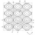
도 1은 본 발명의 일 실시예에 따른 터치 표시 장치를 나타낸 평면도이다. 도 2는 도 1의 제1 터치 전극을 나타내는 평면도이다. 도 3은 도 1의 제2 터치 전극을 나타내는 평면도이다.1 is a plan view of a touch display device according to an embodiment of the present invention. Fig. 2 is a plan view showing the first touch electrode of Fig. 1. Fig. 3 is a plan view showing the second touch electrode of FIG.
도 1 내지 도 3을 참조하면, 본 발명의 일 실시예에 따른 터치 표시장치는 복수의 화소 영역 및 상기 복수의 화소 영역들 사이에 배치되는 제1 터치 전극(320) 및 제2 터치 전극(340)을 포함한다.Referring to FIGS. 1 to 3, a touch display apparatus according to an exemplary embodiment of the present invention includes a plurality of pixel regions, a
상기 복수의 화소 영역은 복수의 제1 화소(10), 복수의 제2 화소(20) 및 복수의 제3 화소(30)를 포함한다.The plurality of pixel regions include a plurality of first pixels (10), a plurality of second pixels (20), and a plurality of third pixels (30).
상기 제1 화소(10)는이웃한 상기 제2 화소(20) 및 상기 제3 화소(30) 대비 작은 면적을 가질 수 있으며, 다각형의 형태 중 사각형의 형태를 가질 수 있다. 본 명세서에서 다각형 내지 사각형은 꼭지점이 라운드진 형태도 포함한다. 즉, 상기 제1 화소(10)는 꼭지점이 라운드진 사각형의 형태를 가질 수 있다.The
상기 제1 화소(10)는 복수이며, 복수의 상기 제1 화소(10)는 서로 동일한 사각형 형태를 가질 수 있다. 복수의 상기 제1 화소(10)는 상호 이격되어 가상의 제1 직선(VL1) 상에 배열되어 있다. 상기 제1 화소(10)는 녹색의 빛을 발광할 수 있으며, 녹색의 빛을 발광하는 유기 발광층을 포함할 수 있다.The
상기 제1 화소(10)의 중심점을 정사각형의 중심점으로 하는 가상의 사각형(VS)의 제1 꼭지점(P1)에 상기 제2 화소(20)가 위치하고 있으며, 가상의 사각형(VS)의 제2 꼭지점(P2)에 상기 제3 화소(30)가 위치하고 있다. 상기 사각형(VS)는 정사각형일 수 있다.The
상기 제2 화소(20)는 상기 제1 화소(10)와 이격되어 있으며, 가상의 정사각형(VS)의 제1 꼭지점(P1)에 중심점이 위치하고 있다. 상기 제2 화소(20)는 이웃하는 상기 제1 화소(10) 대비 더 큰 면적을 가질 수 있으며, 다각형의 형태 중 사각형의 형태를 가질 수 있다. 상기 제2 화소(20)는 복수이며, 복수의 상기 제2 화소(20)는 서로 동일한 사각형의 형태를 가질 수 있다. 상기 제2 화소(20)는 상기 제1 화소(10)를 두고 상호 이격되어 있다. 상기 제2 화소(20)는 청색의 빛을 발광할 수 있으며, 청색의 빛을 발광하는 유기 발광층을 포함할 수 있다.The
상기 제3 화소(30)는상기 제1 화소(10) 및 상기 제2 화소(20)와 이격되어 있으며, 가상의 정사각형(VS)의 제1 꼭지점(P1)과 이웃하는 제2 꼭지점(P2)에 중심점이 위치하고 있다. 상기 제3 화소(30)는 이웃하는 상기 제1 화소(10) 대비 더 큰 면적을 가질 수 있다.The
또한, 상기 제3 화소(30)는 상기 제2 화소(20)와동일한 면적을 가질 수 있으며, 다각형의 형태 중 사각형의 형태를 가질 수 있다. 상기 제3 화소(30)는 복수이며, 복수의 상기 제3 화소(30)는 서로 동일한 사각형의 형태를 가질 수 있다. 복수의 상기 제3 화소(30)는 상기 제1 화소(10)를 두고 상호 이격되어 있다. 상기 제3 화소(30)는 적색의 빛을 발광할 수 있으며, 적색의 빛을 발광하는 유기 발광층을 포함할 수 있다. 그러나, 본 발명은 이에 한정되는 것은 아니며, 상기 제3 화소(30)는 상기 제2 화소(20)와 다른 면적을 가질 수도 있다.In addition, the
복수의 상기 제3 화소(30) 및 복수의 상기 제2 화소(20) 각각은 가상의 제2 직선(VL2) 상에서 상호 교호적으로 배열되며, 이로 인해 제1 꼭지점(P1)에 중심점이 위치하는 복수의 상기 제2 화소(20) 및 제2 꼭지점(P2)에 중심점이 위치하는 복수의 상기 제3 화소(30) 각각은 상기 제1 화소(10)를 둘러싸고 있다.The plurality of
복수의 상기 제2 화소(20) 및 복수의 상기 제3 화소(30) 각각이 상기제1 화소(10)를 둘러싸도록 배열됨으로써, 상기 제1 화소(10), 상기 제2 화소(20) 및 상기 제3 화소(30) 각각의 개구율을 향상시킬 수 있다. 이는 전체적인 유기 발광 표시 장치의 제조 시간 및 제조 비용을 절감하는 동시에 유기 발광 표시 장치가 표시하는 이미지의 품질을 향상시키는 요인으로서 작용된다.The plurality of
즉, 본 발명의 일 실시예에 따른 터치 표시 장치의 화소 배열 구조는 같은 빛을 발광하는 화소 사이의 간격은 넓게 배치되어 증착 신뢰도는 향상되며, 서브 화소를 이루는 적색, 녹색, 청색 화소 사이의 간격은 좁게 배치되어 개구율은 향상되는 구조일 수 있다.That is, in the pixel arrangement structure of the touch display device according to an embodiment of the present invention, the intervals between the pixels emitting the same light are widely arranged to improve the deposition reliability, and the spacing between the red, May be narrowly arranged so that the aperture ratio is improved.
상기 표시 패널 상에는 터치 스크린 패널이 배치된다. 상기 터치 스크린 패널은 제1 터치 전극(320) 및 제2 터치 전극(340)을 포함할 수 있다.A touch screen panel is disposed on the display panel. The touch screen panel may include a
상기 제1 터치 전극(320)은 제1 방향(D1)으로 연장된다. 상기 제1 터치 전극(320)은 지그 재그 형상을 가질 수 있다. 상기 제1 터치 전극(320)은 상기 표시 패널의 화소들 사이에 배치된다. 상기 제1 터치 전극(320)은 상기 제1 화소(10)와 제1 간격(d1)만큼 이격된다. 또한, 제1 터치 전극(320)은 상기 제3 화소(30)와 제2 간격(d2)만큼 이격된다. 즉, 상기 제1 터치 전극(320)과 인접하는 제1 화소(10)의 간격은 상기 제1 터치 전극(320)과 인접하는 제3 화소(30)의 간격과 다른 값을 갖는다. 또한, 상기 제1 터치 전극(320)과 인접하는 제1 화소(10)의 간격은 상기 제1 터치 전극(320)과 인접하는 제2 화소(20)의 간격과 다른 값을 갖는다.The
본 발명의 일 실시예에 따른 표시 패널의 각 화소들은 각각 다른 개구율을 갖는다. 그러나, 이와 중첩하는 터치 전극이 등간격으로 배치되는 경우, 패널을 바라보는 시야각이 증가하게 되면, 각 화소와 터치 전극이 중첩하는 면적비가 달라지게 되고, 이에 따라, 시야각에 따른 각 화소별 휘도비 변화가 달라질 수 있다. 이는 표시 패널의 얼룩 등의 불량으로 나타날 수 있다.Each pixel of the display panel according to an embodiment of the present invention has a different aperture ratio. However, if the overlapping touch electrodes are disposed at equal intervals, the area ratio of overlapping each pixel and the touch electrode becomes different as the viewing angle of the panel increases, and accordingly, the luminance ratio The change can be different. This may be indicated as defects such as stains on the display panel.
그러나, 본 발명의 일 실시예에 따른 터치 스크린 패널의 제1 터치 전극(320)은 각각 다른 개구율을 갖는 각 화소들에 대응하여 다른 간격으로 배치되어, 각 화소별로 화소와 터치 전극이 중첩하는 면적이 조절될 수 있으므로 각 화소의 시야각 증가에 따른 휘도 감소율이 조절될 수 있다. 따라서, 표시 패널의 얼룩 등과 같은 불량을 감소시킬 수 있다.However, the
상기 제2 터치 전극(340)은 상기 제1 방향(D1)과 교차하는 제2 방향(D2)으로 연장된다. 상기 제2 터치 전극(340)은 지그 재그 형상을 가질 수 있다. 상기 제2 터치 전극(340)은 상기 표시 패널의 화소들 사이에 배치된다. 상기 제2 터치 전극(340)은 상기 제1 화소(10)와 제3 간격(d3)만큼 이격된다. 또한, 제1 터치 전극(340)은 상기 제3 화소(30)와 제4 간격(d4)만큼 이격된다. 즉, 상기 제2 터치 전극(340)과 인접하는 제1 화소(10)의 간격은 상기 제2 터치 전극(340)과 인접하는 제3 화소(30)의 간격과 다른 값을 갖는다. 또한, 상기 제2 터치 전극(340)과 인접하는 제1 화소(10)의 간격은 상기 제2 터치 전극(340)과 인접하는 제2 화소(20)의 간격과 다른 값을 갖는다.The
본 발명의 일 실시예에 따른 표시 패널의 각 화소들은 각각 다른 개구율을 갖는다. 그러나, 이와 중첩하는 터치 전극이 등간격으로 배치되는 경우, 패널을 바라보는 시야각이 증가하게 되면, 각 화소와 터치 전극이 중첩하는 면적비가 달라지게 되고, 이에 따라, 시야각에 따른 각 화소별 휘도비 변화가 달라질 수 있다. 이는 표시 패널의 얼룩 등의 불량으로 나타날 수 있다.Each pixel of the display panel according to an embodiment of the present invention has a different aperture ratio. However, if the overlapping touch electrodes are disposed at equal intervals, the area ratio of overlapping each pixel and the touch electrode becomes different as the viewing angle of the panel increases, and accordingly, the luminance ratio The change can be different. This may be indicated as defects such as stains on the display panel.
그러나, 본 발명의 일 실시예에 따른 터치 스크린 패널의 제2 터치 전극(340)은 각각 다른 개구율을 갖는 각화소들에 대응하여 다른 간격으로 배치되어, 각 화소별로 화소와 터치 전극이 중첩하는 면적이 조절될 수 있으므로 각 화소의 시야각 증가에 따른 휘도 감소율이 조절될 수 있다. 따라서, 표시 패널의 얼룩 등과 같은 불량을 감소시킬 수 있다.However, the
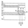
도 4는 도 1의 I-I'라인을 따라 절단한 단면도이다.4 is a cross-sectional view taken along the line I-I 'of FIG.
도 4를 참조하면, 본 발명의 일 실시예에 따른 터치 스크린 패널(300)은 베이스 기판(310), 제1 터치 전극(320), 제1 절연층(330), 제2 터치 전극(340) 및 제2 절연층(350)을 포함한다.4, a touch screen panel 300 according to an exemplary embodiment of the present invention includes a
상기 베이스 기판(310)은 투명 기판일 수 있다. 상기 베이스 기판(310)은 플렉시블(flexible)한 폴리에틸렌테레프탈레이트(PE), 폴리카보네이트(PC), 폴리에틸렌(PE), 폴리비닐클로라이드(PVC), 폴리프로필렌(PP), 폴리스티렌(PS) 또는 폴리메틸메타크릴레이트 메틸에스테르(PMMA)로 이루어진 그룹으로부터 선택된 물질로 제조된 것과 같은 플렉시블(flexible)한 재료로 제조될 수 있다.The
상기 베이스 기판(310)은 터치 표시 장치의 표시 패널을 구성하는 상부 기판일 수 있다. 또는 상기 베이스 기판(310)은 표시 패널 상에 부착되는 별도의 기판일 수 있다. 본 실시예에서는 상기 베이스 기판(310)이 표시 패널 상에 부착되는 별도의 기판으로 도시하였으나, 본 발명은 이에 한정되는 것은 아니다.The
상기 베이스 기판(320) 상에는 제1 터치 전극(320)이 배치된다. 상기 제1 터치 전극(320)은 구리(Cu), 알루미늄(Ti), 몰리브덴(Mo), 티타늄(Ti), 은(Ag), 금(Au), 니켈(Ni), 크롬(Cr), 철(Fe), 인듐(In) 및 갈륨(GA) 등의 저저항 금속 물질을 포함할 수 있다. 그러나, 본 발명은 이에 한정되는 것은 아니며, 상기 제1 터치 전극(320)은 다양한 전도성 물질을 포함할 수 있다.A
상기 제1 터치 전극(320) 상에는 제1 절연층(330)이 배치된다. 상기제1 절연층(330)은 무기 절연 물질을 포함할 수 있다. 예를 들면, 상기 제1 절연층(330)은 실리콘 산화물(SiOx) 또는 실리콘 질화물(SiNx)를 포함할 수 있다. 예를 들면, 상기 제1 절연층(330)은 서로 다른 물질을 포함하는 다층 구조를 가질 수 있다.A first insulating
상기 제1 절연층(330) 상에는 제2 터치 전극(340)이 배치된다. 상기 제2 터치 전극(340)은 구리(Cu), 알루미늄(Ti), 몰리브덴(Mo), 티타늄(Ti), 은(Ag), 금(Au), 니켈(Ni), 크롬(Cr), 철(Fe), 인듐(In) 및 갈륨(GA) 등의 저저항 금속 물질을 포함할 수 있다. 그러나, 본 발명은 이에 한정되는 것은 아니며, 상기 제2 터치 전극(340)은 다양한 전도성 물질을 포함할 수 있다.A
상기 제2 터치 전극(340) 상에는 제2 절연층(350)이 배치된다. 상기제2 절연층(350)은 무기 절연 물질을 포함할 수 있다. 예를 들면, 상기 제2 절연층(350)은 실리콘 산화물(SiOx) 또는 실리콘 질화물(SiNx)를 포함할 수 있다. 예를 들면, 상기 제2 절연층(350)은 서로 다른 물질을 포함하는 다층 구조를 가질 수 있다.A second insulating layer 350 is disposed on the
도 5 내지 도 6은 도 4의 터치 스크린 패널의 제조 방법을 설명하기 위한 단면도들이다.5 to 6 are cross-sectional views illustrating a method of manufacturing the touch screen panel of FIG.
도 5를 참조하면, 베이스 기판(310) 상에 제1 터치 전극(320) 및 제1 절연층(330)이 형성된다.Referring to FIG. 5, a
상기 베이스 기판(310)은 터치 표시 장치의 표시 패널을 구성하는 상부 기판일 수 있다. 또는 상기 베이스 기판(310)은 표시 패널 상에 부착되는 별도의 기판일 수 있다. 본 실시예에서는 상기 베이스 기판(310)이 표시 패널 상에 부착되는 별도의 기판으로 도시하였으나, 본 발명은 이에 한정되는 것은 아니다.The
상기 베이스 기판(320) 상에는 제1 터치 전극(320)이 형성된다. 상기 제1 터치 전극(320)은 구리(Cu), 알루미늄(Ti), 몰리브덴(Mo), 티타늄(Ti), 은(Ag), 금(Au), 니켈(Ni), 크롬(Cr), 철(Fe), 인듐(In) 및 갈륨(GA)등의 저저항 금속 물질을 포함할 수 있다. 그러나, 본 발명은 이에 한정되는 것은 아니며, 상기 제1 터치 전극(320)은 다양한 전도성 물질을 포함할 수 있다.A
상기 제1 터치 전극(320) 상에는 제1 절연층(330)이 형성된다. 상기제1 절연층(330)은 무기 절연 물질을 포함할 수 있다. 예를 들면, 상기 제1 절연층(330)은 실리콘 산화물(SiOx) 또는 실리콘 질화물(SiNx)를 포함할 수 있다. 예를 들면, 상기 제1 절연층(330)은 서로 다른 물질을 포함하는 다층 구조를 가질 수 있다.A
도 6을 참조하면, 상기 제1 절연층(330)이 형성된 상기 베이스 기판(310) 상에 제2 터치 전극이 형성된다.Referring to FIG. 6, a second touch electrode is formed on the
상기 제1 절연층(330) 상에는 제2 터치 전극(340)이 형성된다. 상기 제2 터치 전극(340)은 구리(Cu), 알루미늄(Ti), 몰리브덴(Mo), 티타늄(Ti), 은(Ag), 금(Au), 니켈(Ni), 크롬(Cr), 철(Fe), 인듐(In) 및 갈륨(GA)등의 저저항 금속 물질을 포함할 수 있다. 그러나, 본 발명은 이에 한정되는 것은 아니며, 상기 제2 터치 전극(340)은 다양한 전도성 물질을 포함할 수 있다.A
도 4를 참조하면, 상기 제2 터치 전극(340)이 형성된 베이스 기판(310) 상에 제2 절연층(350)이 형성된다.Referring to FIG. 4, a second insulating layer 350 is formed on a
상기 제2 터치 전극(340) 상에는 제2 절연층(350)이 배치된다. 상기제2 절연층(350)은 무기 절연 물질을 포함할 수 있다. 예를 들면, 상기 제2 절연층(350)은 실리콘 산화물(SiOx) 또는 실리콘 질화물(SiNx)를 포함할 수 있다. 예를 들면, 상기 제2 절연층(350)은 서로 다른 물질을 포함하는 다층 구조를 가질 수 있다.A second insulating layer 350 is disposed on the
상기 터치 스크린 패널(300)은 표시 패널에 부착된다. 그러나, 상기 베이스 기판(310)이 터치 표시 장치의 표시 패널을 구성하는 상부 기판인 경구, 표시 패널 상에 상기 터치 스크린 패널(300)이 직접 형성될 수 도 있다.The touch screen panel 300 is attached to the display panel. However, the touch screen panel 300 may be formed directly on the display panel, which is the upper substrate, on which the
도 7은 본 발명의 일 실시예에 따른 표시 패널을 나타낸 평면도이다.7 is a plan view of a display panel according to an embodiment of the present invention.
도 7을 참조하면, 본 발명의 일 실시예에 따른 터치 표시 장치는 표시 패널(DP) 및 터치 스크린 패널(300)을 포함한다. 본 실시예에서 상기 터치 표시 장치는 유기발광 터치 표시 장치일 수 있다.Referring to FIG. 7, a touch display apparatus according to an embodiment of the present invention includes a display panel DP and a touch screen panel 300. In this embodiment, the touch display device may be an organic light emitting touch display device.
상기 표시 패널(DP)은 하부 기판(100), 버퍼층(102), 게이트 절연막(104), 층간절연막(106), 평탄절연막(108), 화소정의막(112), 박막트랜지스터(130), 제1 전극(146), 제2 전극(148), 유기 발광 소자(200) 및 밀봉 기판(150)을 포함한다.The display panel DP includes a lower substrate 100, a buffer layer 102, a
하부 기판(100)은 투명 절연 기판을 포함할 수 있다. 예를 들면, 제1 기판(100)은 유리 기판, 석영 기판, 투명 수지 기판 등으로 구성될 수 있다. 여기서, 상기 투명 수지 기판은 폴리이미드계 수지, 아크릴계 수지, 폴리아크릴레이트계 수지, 폴리카보네이트계 수지, 폴리에테르계 수지, 폴리에틸렌 테레프탈레이트계 수지, 술폰산계 수지 등을 포함할 수 있다.The lower substrate 100 may include a transparent insulating substrate. For example, the first substrate 100 may be composed of a glass substrate, a quartz substrate, a transparent resin substrate, or the like. Here, the transparent resin substrate may include a polyimide resin, an acrylic resin, a polyacrylate resin, a polycarbonate resin, a polyether resin, a polyethylene terephthalate resin, a sulfonic acid resin, or the like.
버퍼층(102)은 하부 기판(100) 상에 배치되고, 절연물질을 포함한다. 버퍼층(102)에 사용될 수 있는 절연물질의 예로는, 실리콘 산화물(SiOx), 실리콘 질화물(SiNx), 실리콘 산질화물(SiOxNy), 실리콘 산탄화물(SiOxCy), 실리콘 탄질화물(SiCxNy) 등의 무기절연물질을 포함한다. 상기 무기 절연물질들은 단독으로, 서로 조합된 화합물, 혼합물, 또는 적층구조물로 사용될 수 있다. 상기 버퍼층(102)이 적층구조물을 포함하는 경우, 실리콘 산화막, 실리콘 질화막, 실리콘 산질화막, 실리콘 산탄화막 및/또는 실리콘 탄질화막을 포함하는 다층 구조로 형성될 수 있다.The buffer layer 102 is disposed on the lower substrate 100 and includes an insulating material. Examples of the insulating material that can be used for the buffer layer 102 include inorganic insulating materials such as silicon oxide (SiOx), silicon nitride (SiNx), silicon oxynitride (SiOxNy), silicon oxycarbide (SiOxCy), silicon carbonitride (SiCxNy) ≪ / RTI > The inorganic insulating materials may be used alone, as a compound, a mixture, or a laminated structure mutually combined. When the buffer layer 102 includes a stacked structure, the buffer layer 102 may be formed in a multi-layer structure including a silicon oxide layer, a silicon nitride layer, a silicon oxynitride layer, a silicon oxynitride layer, and / or a silicon carbide layer.
상기 버퍼층(102)은 하부 기판(100)으로부터 금속 원자들이나 불순물들이 확산되는 현상을 방지하며, 후속하여 액티브 패턴(132, 134, 136)을 형성하기 위한 결정화 공정 동안 열의 전달 속도를 조절하여 액티브 패턴의 전기적 특성을 향상시킨다. 또한, 상기 버퍼층(102)은 하부 기판(100)의 표면을 평탄화시킨다.The buffer layer 102 prevents the diffusion of metal atoms or impurities from the lower substrate 100 and subsequently controls the heat transfer rate during the crystallization process to form the
상기 액티브 패턴(135)은 상기 버퍼층(102) 상에 배치된다. 본 실시예에서, 상기 액티브 패턴(135)은 폴리실리콘을 포함한다. 상기 액티브 패턴(135)은 박막트랜지스터(130)의 드레인 전극(142)과 콘택되는 드레인 콘택부(132), 박막트랜지스터(130)의 소스 전극(144)과 콘택되는 소스 콘택부(136) 및 드레인 콘택부(132)와 소스 콘택부(136)의 사이에 배치되는 채널부(134)를 포함한다.The
게이트 절연막(104)은 상기 액티브 패턴(135)이 형성된 버퍼층(102) 상에 배치되어 액티브 패턴(135)을 게이트 전극(138) 및 게이트 라인(도시되지 않음)과 전기적으로 절연시킨다. 게이트 절연막(104)은 실리콘 산화물, 금속 산화물 등을 사용하여 형성될 수 있다. 예를 들면, 게이트 절연막(115)을 구성하는 금속 산화물은 하프늄 산화물(HfOx), 알루미늄 산화물(AlOx), 지르코늄 산화물(ZrOx), 티타늄 산화물(TiOx), 탄탈륨 산화물(TaOx) 등을 포함할 수 있다. 이들은 단독으로 또는 서로 조합되거나 적층되어 사용될 수 있다. 게이트 절연막(104)은 액티브 패턴(135)은 소스 콘택부(136) 및 드레인 콘택부(132)를 노출하는 콘택홀들을 포함한다.The
게이트 전극(138)은 게이트 절연막(104) 상에 배치된다. 게이트 전극(138)은 액티브 패턴(135)의 채널부(134) 상에 배치된다. 게이트 전극(138)과 소스 전극(144) 사이에 전압차가 형성되는 경우, 박막 트랜지스터(130)가 턴온되어 채널부(134)를 통하여 드레인 전극(142)으로 전류가 흐른다.The
게이트 전극(138)은 금속, 합금, 금속 질화물, 도전성 금속 산화물, 투명 도전성 물질 등을 사용하여 형성될 수 있다. 예를 들면, 게이트 전극(138)은 알루미늄(Al), 알루미늄을 함유하는 합금, 알루미늄 질화물(AlNx), 은(Ag), 은을 함유하는 합금, 텅스텐(W), 텅스텐 질화물(WNx), 구리(Cu), 구리를 함유하는 합금, 니켈(Ni), 크롬(Cr), 크롬 질화물(CrNx), 몰리브데늄(Mo), 몰리브데늄을 함유하는 합금, 티타늄(Ti), 티타늄 질화물(TiNx), 백금(Pt), 탄탈륨(Ta), 탄탈륨 질화물(TaNx), 네오디뮴(Nd), 스칸듐(Sc), 스트론튬 루테늄 산화물(SRO), 아연 산화물(ZnOx), 인듐 주석 산화물(ITO), 주석 산화물(SnOx), 인듐 산화물(InOx), 갈륨 산화물(GaOx), 인듐 아연 산화물(IZO) 등을 포함할 수 있다. 이들은 단독으로 또는 서로 조합되어 사용될 수 있다. 또한, 게이트 전극(138)은 금속막, 합금막, 금속 질화물막, 도전성 금속 산화물막 및/또는 투명 도전성 물질막을 포함하는 단층 구조 또는 다층 구조로 형성될 수 있다.The
층간절연막(106)은 게이트 전극(138) 및 게이트 라인(도시되지 않음)이 형성된 게이트 절연막(104) 상에 형성된다. 층간절연막(106)은 게이트 전극(138) 및 게이트 라인(도시되지 않음)을 소스 전극(144) 및 드레인 전극(142)과 절연시킨다.An interlayer insulating
상기 층간 절연막(106)은 실리콘 화합물을 포함할 수 있다. 예를 들면, 층간 절연막(125)은 실리콘 산화물, 실리콘 질화물, 실리콘 산질화물, 실리콘 탄질화물, 실리콘 산탄화물 등을 사용하여 형성될 수 있다. 이들은 단독으로 또는 서로 조합되어 사용될 수 있다. 층간 절연막(106)은 액티브 패턴(135)의 소스부(136) 및 드레인부(132)를 노출하는 콘택홀들을 포함한다.The interlayer insulating
상기 소스 전극(144) 및 상기 드레인 전극(142)은 층간 절연막(106) 상에 형성된다. 상기 소스 전극(144) 및 상기 드레인 전극(142)은 상기 콘택홀들을 관통하여 액티브 패턴(132)의 소스부(136) 및 드레인부(132)에 각각 콘택된다.The
상기 소스 및 드레인 전극(144, 142)은 각기 금속, 합금, 금속 질화물, 도전성 금속 산화물, 투명 도전성 물질 등을 사용하여 형성될 수 있다. 예를 들면, 소스 및 드레인 전극(144, 142)은 각기 알루미늄, 알루미늄을 함유하는 합금, 알루미늄 질화물, 은, 은을 함유하는 합금, 텅스텐, 텅스텐 질화물, 구리, 구리를 함유하는 합금, 니켈, 크롬, 크롬 질화물, 몰리브데늄, 몰리브데늄을 함유하는 합금, 티타늄, 티타늄 질화물, 백금, 탄탈륨, 탄탈륨 질화물, 네오디뮴, 스칸듐, 스트론튬 루테늄 산화물, 아연 산화물, 인듐 주석 산화물, 주석 산화물, 인듐 산화물, 갈륨 산화물, 인듐 아연 산화물 등을 포함할 수 있다. 이들은 단독으로 또는 서로 조합되어 사용될 수 있다.Each of the source and drain
평탄 절연막(108)은 소스 및 드레인 전극(144, 142) 및 데이터 라인(도시되지 않음)이 형성된 층간절연막(106) 상에 형성되어 소스전극(144)을 제1 전극(146)과 절연시킨다.The flat
상기 평탄 절연막(108)은 유기절연물질 또는 무기절연물질을 포함한다. 예를 들면, 평탄 절연막(108)은 포토레지스트, 아크릴계 수지, 폴리이미드계 수지, 폴리아미드계 수지, 실록산계 수지, 감광성 아크릴 카르복실기를 포함하는 수지, 노볼락 수지, 알칼리 가용성 수지, 실리콘 산화물, 실리콘 질화물, 실리콘 산질화물, 실리콘 산탄화물, 실리콘 탄질화물 등을 포함할 수 있다. 이들은 단독으로 또는 서로 조합되어 사용될 수 있다.The flat
상기 평탄 절연막(108)은 드레인 전극(142)을 노출시키는 콘택홀을 포함한다.The flat
제1 전극(146)은 화소 영역에 대응되는 평탄절연막(108) 상에 배치되고 평탄절연막(108)의 콘택홀을 통하여 드레인 전극(142)에 전기적으로 연결된다.The
상기 유기 발광 표시 장치가 전면 발광 방식을 가질 경우, 제1 전극(146)은 반사성을 갖는 금속, 반사성을 갖는 합금 등을 사용하여 형성될 수 있다. 예를 들면, 제1 전극(146)은 알루미늄, 은, 백금, 금(Au), 크롬, 텅스텐, 몰리브데늄, 티타늄, 팔라듐(Pd), 이리듐(Ir), 이들 금속의 합금 등을 포함할 수 있다. 이들은 단독으로 또는 서로 조합되어 사용될 수 있다. 다른 실시예에서, 제1 전극(146)은 인듐 주석 산화물, 주석 산화물, 인듐 아연 산화물, 아연 산화물, 인듐 갈륨 산화물, 갈륨 산화물 등과 같은 투명 도전성 물질을 사용하여 형성될 수 있다. 이들은 단독으로 또는 서로 조합되어 사용될 수 있다.When the organic light emitting display device has a top emission type, the
화소정의막(112)은 제1 전극(146)이 형성된 평탄 절연막(108) 상에 배치되어 제1 전극(146)의 일부를 노출시킨다. 화소 정의막(112)은 유기물질이나 무기 물질을 사용하여 형성될 수 있다. 예를 들면, 화소 정의막(112)은 포토레지스트, 폴리아크릴계 수지, 폴리이미드계 수지, 아크릴계 수지, 실리콘 화합물 등을 사용하여 형성될 수 있다. 화소 정의막(112)에 의해 제1 전극(146)이 노출된 부분에 의해 상기 유기 발광 표시 장치의 표시 영역과 비표시 영역이 정의될 수 있다. 예를 들면, 화소 정의막(112)에 의해 제1 전극(146)이 노출된 부분이 위치하는 부분이 상기 표시 영역에 해당될 수 있다.The
유기 발광 소자(200)는 화소 정의막(112)에 의해 노출된 제1 전극(146) 상에 배치되고, 제2 전극은 유기 발광 소자(200) 및 화소정의막(112)을 커버한다.The organic light emitting diode 200 is disposed on the
상기 유기 발광 표시 장치가 전면 발광 방식을 가질 경우, 제2 전극(148)은 인듐 주석 산화물, 주석 산화물, 인듐 아연 산화물, 아연 산화물, 인듐 갈륨 산화물, 갈륨 산화물 등과 같은 투명 도전성 물질을 사용하여 형성될 수 있다. 이들은 단독으로 또는 서로 조합되어 사용될 수 있다.The second electrode 148 may be formed using a transparent conductive material such as indium tin oxide, tin oxide, indium zinc oxide, zinc oxide, indium gallium oxide, gallium oxide, or the like . These may be used alone or in combination with each other.
도 8은 본 발명의 일 실시예에 따른 터치 표시 장치를 나타낸 평면도이다. 도 9는 도 8의 제1 터치 전극을 나타내는 평면도이다. 도 10은 도 8의 제2 터치 전극을 나타내는 평면도이다.8 is a plan view of a touch display device according to an embodiment of the present invention. 9 is a plan view showing the first touch electrode of FIG. 10 is a plan view showing the second touch electrode of FIG.
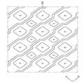
도 8 내지 도 10을 참조하면, 본 발명의 일 실시예에 따른 터치 표시장치는 복수의 화소 영역 및 상기 복수의 화소 영역들 사이에 배치되는 제1 터치 전극(1320) 및 제2 터치 전극(1340)을 포함한다.8-10, a touch display device according to an embodiment of the present invention includes a plurality of pixel regions, a
상기 복수의 화소 영역은 복수의 제1 화소(10), 복수의 제2 화소(20) 및 복수의 제3 화소(30)를 포함한다.The plurality of pixel regions include a plurality of first pixels (10), a plurality of second pixels (20), and a plurality of third pixels (30).
상기 제1 화소(10)는 이웃한 상기 제2 화소(20) 및 상기 제3 화소(30) 대비 작은 면적을 가질 수 있으며, 다각형의 형태 중 사각형의 형태를 가질 수 있다. 본 명세서에서 다각형 내지 사각형은 꼭지점이 라운드진 형태도 포함한다. 즉, 상기 제1 화소(10)는 꼭지점이 라운드진 사각형의 형태를 가질 수 있다.The
상기 제1 화소(10)는 복수이며, 복수의 상기 제1 화소(10)는 서로 동일한 사각형 형태를 가질 수 있다. 복수의 상기 제1 화소(10)는 상호 이격되어 가상의 제1 직선(VL1) 상에 배열되어 있다. 상기 제1 화소(10)는 녹색의 빛을 발광할 수 있으며, 녹색의 빛을 발광하는 유기 발광층을 포함할 수 있다.The
상기 제1 화소(10)의 중심점을 정사각형의 중심점으로 하는 가상의 사각형(VS)의 제1 꼭지점(P1)에 상기 제2 화소(20)가 위치하고 있으며, 가상의 사각형(VS)의 제2 꼭지점(P2)에 상기 제3 화소(30)가 위치하고 있다. 상기 사각형(VS)는 정사각형일 수 있다.The
상기 제2 화소(20)는 상기 제1 화소(10)와 이격되어 있으며, 가상의 정사각형(VS)의 제1 꼭지점(P1)에 중심점이 위치하고 있다. 상기 제2 화소(20)는 이웃하는 상기 제1 화소(10) 대비 더 큰 면적을 가질 수 있으며, 다각형의 형태 중 사각형의 형태를 가질 수 있다. 상기 제2 화소(20)는 복수이며, 복수의 상기 제2 화소(20)는 서로 동일한 사각형의 형태를 가질 수 있다. 상기 제2 화소(20)는 상기 제1 화소(10)를 두고 상호 이격되어 있다. 상기 제2 화소(20)는 청색의 빛을 발광할 수 있으며, 청색의 빛을 발광하는 유기 발광층을 포함할 수 있다.The
상기 제3 화소(30)는 상기 제1 화소(10) 및 상기 제2 화소(20)와 이격되어 있으며, 가상의 정사각형(VS)의 제1 꼭지점(P1)과 이웃하는 제2 꼭지점(P2)에 중심점이 위치하고 있다. 상기 제3 화소(30)는 이웃하는 상기 제1 화소(10) 대비 더 큰 면적을 가질 수 있다.The
또한, 상기 제3 화소(30)는 상기 제2 화소(20)와 동일한 면적을 가질 수 있으며, 다각형의 형태 중 사각형의 형태를 가질 수 있다. 상기 제3 화소(30)는 복수이며, 복수의 상기 제3 화소(30)는 서로 동일한 사각형의 형태를 가질 수 있다. 복수의 상기 제3 화소(30)는 상기 제1 화소(10)를 두고 상호 이격되어 있다. 상기 제3 화소(30)는 적색의 빛을 발광할 수 있으며, 적색의 빛을 발광하는 유기 발광층을 포함할 수 있다. 그러나, 본 발명은 이에 한정되는 것은 아니며, 상기 제3 화소(30)는 상기 제2 화소(20)와 다른 면적을 가질 수도 있다.Also, the
복수의 상기 제3 화소(30) 및 복수의 상기 제2 화소(20) 각각은 가상의 제2 직선(VL2) 상에서 상호 교호적으로 배열되며, 이로 인해 제1 꼭지점(P1)에 중심점이 위치하는 복수의 상기 제2 화소(20) 및 제2 꼭지점(P2)에 중심점이 위치하는 복수의 상기 제3 화소(30) 각각은 상기 제1 화소(10)를 둘러싸고 있다.The plurality of
복수의 상기 제2 화소(20) 및 복수의 상기 제3 화소(30) 각각이 상기제1 화소(10)를 둘러싸도록 배열됨으로써, 상기 제1 화소(10), 상기 제2 화소(20) 및 상기 제3 화소(30) 각각의 개구율을 향상시킬 수 있다. 이는 전체적인 유기 발광 표시 장치의 제조 시간 및 제조 비용을 절감하는 동시에 유기 발광 표시 장치가 표시하는 이미지의 품질을 향상시키는 요인으로서 작용된다.The plurality of
즉, 본 발명의 일 실시예에 따른 터치 표시 장치의 화소 배열 구조는 같은 빛을 발광하는 화소 사이의 간격은 넓게 배치되어 증착 신뢰도는 향상되며, 서브 화소를 이루는 적색, 녹색, 청색 화소 사이의 간격은 좁게 배치되어 개구율은 향상되는 구조일 수 있다.That is, in the pixel arrangement structure of the touch display device according to an embodiment of the present invention, the intervals between the pixels emitting the same light are widely arranged to improve the deposition reliability, and the spacing between the red, May be narrowly arranged so that the aperture ratio is improved.
상기 표시 패널 상에는 터치 스크린 패널이 배치된다. 상기 터치 스크린 패널은 제1 터치 전극(320) 및 제2 터치 전극(340)을 포함할 수 있다.A touch screen panel is disposed on the display panel. The touch screen panel may include a
상기 제1 터치 전극(320)은 제1 방향(D1)으로 연장된다. 상기 제1 터치 전극(320)은 지그 재그 형상을 가질 수 있다. 상기 제1 터치 전극(320)은 상기 표시 패널의 화소들 사이에 배치된다. 상기 제1 터치 전극(320)은 상기 제1 화소(10)와 제1 간격(d1)만큼 이격된다. 또한, 제1 터치 전극(320)은 상기 제3 화소(30)와 제2 간격(d2)만큼 이격된다. 즉, 상기 제1 터치 전극(320)과 인접하는 제1 화소(10)의 간격은 상기 제1 터치 전극(320)과 인접하는 제3 화소(30)의 간격과 다른 값을 갖는다. 또한, 상기 제1 터치 전극(320)과 인접하는 제1 화소(10)의 간격은 상기 제1 터치 전극(320)과 인접하는 제2 화소(20)의 간격과 다른 값을 갖는다.The
상기 표시 패널 상에는 터치 스크린 패널이 배치된다. 상기 터치 스크린 패널은 제1 터치 전극(1320) 및 제2 터치 전극(1340)을 포함할 수 있다.A touch screen panel is disposed on the display panel. The touch screen panel may include a
상기 제1 터치 전극(1320)은 제1 방향(D1)으로 연장된다. 상기 제1 터치 전극(1320)은 지그 재그 형상을 가질 수 있다. 상기 제1 터치 전극(1320)은 상기 표시 패널의 화소들 사이에 배치된다. 상기 제1 터치 전극(1320)은 상기 제1 화소(10)와 제1 간격(d1)만큼 이격된다. 또한, 제1 터치 전극(1320)은 상기 제3 화소(30)와 제2 간격(d2)만큼 이격된다. 즉, 상기 제1 터치 전극(1320)과 인접하는 제1 화소(10)의 간격은 상기 제1 터치 전극(1320)과 인접하는 제3 화소(30)의 간격과 다른 값을 갖는다. 또한, 상기 제1 터치 전극(1320)과 인접하는 제1 화소(10)의 간격은 상기 제1 터치 전극(1320)과 인접하는 제2 화소(20)의 간격과 다른 값을 갖는다.The
본 발명의 일 실시예에 따른 표시 패널의 각 화소들은 각각 다른 개구율을 갖는다. 그러나, 이와 중첩하는 터치 전극이 등간격으로 배치되는 경우, 패널을 바라보는 시야각이 증가하게 되면, 각 화소와 터치 전극이 중첩하는 면적비가 달라지게 되고, 이에 따라, 시야각에 따른 각 화소별 휘도비 변화가 달라질 수 있다. 이는 표시 패널의 얼룩 등의 불량으로 나타날 수 있다.Each pixel of the display panel according to an embodiment of the present invention has a different aperture ratio. However, if the overlapping touch electrodes are disposed at equal intervals, the area ratio of overlapping each pixel and the touch electrode becomes different as the viewing angle of the panel increases, and accordingly, the luminance ratio The change can be different. This may be indicated as defects such as stains on the display panel.
그러나, 본 발명의 일 실시예에 따른 터치 스크린 패널의 제1 터치 전극(1320)은 각각 다른 개구율을 갖는 각 화소들에 대응하여 다른 간격으로 배치되어, 각 화소별로 화소와 터치 전극이 중첩하는 면적이 조절될 수 있으므로 각 화소의 시야각 증가에 따른 휘도 감소율이 조절될 수 있다. 따라서, 표시 패널의 얼룩 등과 같은 불량을 감소시킬 수 있다.However, the
상기 제2 터치 전극(1340)은 상기 제1 방향(D1)과 교차하는 제2 방향(D2)으로 연장된다. 상기 제2 터치 전극(1340)은 지그 재그 형상을 가질 수 있다. 상기 제2 터치 전극(1340)은 상기 표시 패널의 화소들 사이에 배치된다. 상기 제2 터치 전극(1340)은 제1 가지부(1341) 및 상기 제1 가지부(1341)에 연결되고 상기 제1 화소(10)를 둘러싸는 제2 가지부(1343)를 포함한다. 상기 제2 터치 전극(1340)은 상기 제1 화소(10)와 제3 간격(d3)만큼 이격된다. 또한, 제1 터치 전극(1340)은 상기 제3 화소(30)와 제4 간격(d4)만큼 이격된다. 즉, 상기 제2 터치 전극(1340)과 인접하는 제1 화소(10)의 간격은 상기 제2 터치 전극(1340)과 인접하는 제3 화소(30)의 간격과 다른 값을 갖는다. 또한, 상기 제2 터치 전극(1340)과 인접하는 제1 화소(10)의 간격은 상기 제2 터치 전극(1340)과 인접하는 제2 화소(20)의 간격과 다른 값을 갖는다.The
본 발명의 일 실시예에 따른 표시 패널의 각 화소들은 각각 다른 개구율을 갖는다. 그러나, 이와 중첩하는 터치 전극이 등간격으로 배치되는 경우, 패널을 바라보는 시야각이 증가하게 되면, 각 화소와 터치 전극이 중첩하는 면적비가 달라지게 되고, 이에 따라, 시야각에 따른 각 화소별 휘도비 변화가 달라질 수 있다. 이는 표시 패널의 얼룩 등의 불량으로 나타날 수 있다.Each pixel of the display panel according to an embodiment of the present invention has a different aperture ratio. However, if the overlapping touch electrodes are disposed at equal intervals, the area ratio of overlapping each pixel and the touch electrode becomes different as the viewing angle of the panel increases, and accordingly, the luminance ratio The change can be different. This may be indicated as defects such as stains on the display panel.
그러나, 본 발명의 일 실시예에 따른 터치 스크린 패널의 제2 터치 전극(1340)은 각각 다른 개구율을 갖는 각 화소들에 대응하여 다른 간격으로 배치되어, 각 화소별로 화소와 터치 전극이 중첩하는 면적이 조절될 수 있으므로 각 화소의 시야각 증가에 따른 휘도 감소율이 조절될 수 있다. 따라서, 표시 패널의 얼룩 등과 같은 불량을 감소시킬 수 있다.However, the
본 발명의 실시예들에 따르면, 화소 배열 구조는 같은 빛을 발광하는 화소 사이의 간격은 넓게 배치되어 증착 신뢰도는 향상되며, 서브 화소를 이루는 적색, 녹색, 청색 화소 사이의 간격은 좁게 배치되어 개구율은 향상될 수 있다.According to the embodiments of the present invention, the pixel arrangement structure is arranged such that the intervals between the pixels emitting the same light are wide so that the deposition reliability is improved, and the spacing between the red, green and blue pixels constituting the sub- Can be improved.
또한, 터치 스크린 패널의 터치 전극들은 각각 다른 개구율을 갖는 각 화소들에 대응하여, 서로 다른 간격으로 배치되어, 각 화소별로 화소와 터치 전극이 중첩하는 면적이 조절될 수 있으므로 각 화소의 시야각 증가에 따른 휘도 감소율이 조절될 수 있다. 따라서, 표시 패널의 얼룩 등과 같은 불량을 감소시킬 수 있다.In addition, since the touch electrodes of the touch screen panel are arranged at different intervals corresponding to the respective pixels having different aperture ratios, and the overlapping area of the pixels and the touch electrodes can be adjusted for each pixel, The luminance reduction rate can be adjusted. Therefore, defects such as unevenness of the display panel can be reduced.
이상에서는 실시예들을 참조하여 설명하였지만, 해당 기술 분야의 숙련된 통상의 기술자는 하기의 특허 청구의 범위에 기재된 본 발명의 사상 및 영역으로부터 벗어나지 않는 범위 내에서 본 발명을 다양하게 수정 및 변경시킬 수 있음을 이해할 수 있을 것이다.While the present invention has been particularly shown and described with reference to exemplary embodiments thereof, it will be understood by those skilled in the art that various changes and modifications may be made therein without departing from the spirit and scope of the invention as defined by the appended claims. It can be understood that.
310: 베이스 기판310: 제1 터치 전극
330: 제1 절연층340: 제2 터치 전극
350: 제2 절연층310: base substrate 310: first touch electrode
330: first insulating layer 340: second touch electrode
350: second insulating layer
Claims (20)
Translated fromKorean상기 표시 패널 상에 배치되는 터치 스크린 패널을 포함하고,
상기 터치 스크린 패널은,
제1 방향으로 연장되고, 평면도 상에서 상기 화소 영역들 사이에 배치되는 제1 터치 전극; 및
상기 제1 방향과 교차하는 제2 방향으로 연장되고, 평면도 상에서 상기 화소 영역들 사이에 배치되는 제2 터치 전극을 포함하고,
상기 복수의 화소 영역은,
제1 화소;
상기 제1 화소와 이격되어 있으며, 상기 제1 화소의 중심점을 사각형의 중심점으로 하는 가상의 사각형의 제1 꼭지점에 중심점이 위치하는 제2 화소; 및
상기 제2 화소와 이격되어 있으며, 상기 가상의 사각형의 상기 제1 꼭지점과 이웃하는 제2 꼭지점에 중심점이 위치하는 제3 화소를 포함하며,
상기 제1 화소는 제1 면적을 갖고, 상기 제2 화소 및 상기 제3 화소는 상기 제1 면적보다 큰 제2 면적을 가지고,
상기 제1 터치 전극 및 상기 제2 터치 전극은 상기 제1 화소와 제1 간격만큼 이격되고, 상기 제2 화소 또는 상기 제3 화소와 상기 제1 간격보다 큰 제2 간격만큼 이격되는 것을 특징으로 하는 터치 표시 장치.A display panel including a plurality of pixel regions separated by a non-pixel region; And
And a touch screen panel disposed on the display panel,
The touch screen panel includes:
A first touch electrode extending in a first direction and arranged between the pixel regions in a plan view; And
And a second touch electrode extending in a second direction intersecting with the first direction and disposed between the pixel regions in a plan view,
Wherein the plurality of pixel regions include:
A first pixel;
A second pixel spaced apart from the first pixel and having a center point at a first vertex of a virtual rectangle having a center point of the first pixel as a center point of the rectangle; And
A third pixel spaced apart from the second pixel and having a center point at a second vertex adjacent to the first vertex of the virtual quadrilateral,
Wherein the first pixel has a first area, the second pixel and the third pixel have a second area larger than the first area,
Wherein the first touch electrode and the second touch electrode are spaced apart from each other by a first gap and a second gap larger than the first gap from the second pixel or the third pixel, Touch display device.
상기 제2 터치 전극은,
제1 가지부; 및
상기 제1 가지부에 연결되고 상기 제1 화소를 둘러싸는 제2 가지부를 포함하는 것을 특징으로 하는 터치 표시 장치.The method according to claim 1,
The second touch electrode includes:
A first branch; And
And a second branch portion connected to the first branch portion and surrounding the first pixel.
상기 제2 화소는 복수이며,
상기 복수의 제2 화소는 상기 제1 화소를 사이에 두로 상호 이격되어 있는 것을 특징으로 하는 터치 표시 장치.The method according to claim 1,
Wherein the second pixel includes a plurality of pixels,
Wherein the plurality of second pixels are spaced apart from each other by the first pixel.
상기 제3 화소는 복수이며,
상기 복수의 제3 화소는 상기 제1 화소를 사이에 두로 상호 이격되어 있는 것을 특징으로 하는 터치 표시 장치.The method according to claim 1,
The third pixel is a plurality of pixels,
Wherein the plurality of third pixels are spaced apart from each other by the first pixel.
상기 제2 화소 및 상기 제3 화소는 복수이며,
상기 복수의 제2 화소 및 상기 복수의 제3 화소는 상기 제1 화소를 둘러싸도록 가상의 직선상에서 서로 교호적으로 배열되는 것을 특징으로 하는 터치 표시 장치.The method according to claim 1,
The second pixel and the third pixel are plural,
Wherein the plurality of second pixels and the plurality of third pixels are alternately arranged on an imaginary straight line so as to surround the first pixels.
상기 제1 화소, 상기 제2 화소 및 상기 제3 화소는 각각 서로 다른 색의 빛을 발광하는 것을 특징으로 하는 터치 표시 장치.The method according to claim 1,
Wherein the first pixel, the second pixel, and the third pixel emit light of different colors, respectively.
상기 제1 화소는 녹색, 상기 제2 화소는 청색, 상기 제3 화소는 적색의 빛을 발광하는 것을 특징으로 하는 터치 표시 장치.The method according to claim 1,
Wherein the first pixel emits green light, the second pixel emits blue light, and the third pixel emits red light.
제1 방향으로 연장되고, 평면도 상에서 상기 화소 영역들 사이에 배치되는 제1 터치 전극을 형성하는 단계; 및
상기 제1 방향과 교차하는 제2 방향으로 연장되고, 평면도 상에서 상기 화소 영역들 사이에 배치되는 제2 터치 전극을 형성하는 단계를 포함하고,
상기 표시 패널을 형성하는 단계는,
제1 화소를 형성하는 단계;
상기 제1 화소와 이격되어 있으며, 상기 제1 화소의 중심점을 사각형의 중심점으로 하는 가상의 사각형의 제1 꼭지점에 중심점이 위치하는 제2 화소를 형성하는 단계; 및
상기 제2 화소와 이격되어 있으며, 상기 가상의 사각형의 상기 제1 꼭지점과 이웃하는 제2 꼭지점에 중심점이 위치하는 제3 화소를 형성하는 단계를 포함하며,
상기 제1 화소는 제1 면적을 갖고, 상기 제2 화소 및 상기 제3 화소는 상기 제1 면적보다 큰 제2 면적을 가지고,
상기 제1 터치 전극 및 상기 제2 터치 전극은 상기 제1 화소와 제1 간격만큼 이격되고, 상기 제2 화소 또는 상기 제3 화소와 상기 제1 간격보다 큰 제2 간격만큼 이격되는 것을 특징으로 하는 터치 표시 장치의 제조 방법.Forming a display panel including a plurality of pixel regions separated by a non-pixel region;
Forming a first touch electrode extending in a first direction and being disposed between the pixel regions in a plan view; And
Forming a second touch electrode extending in a second direction intersecting with the first direction and disposed between the pixel regions in a plan view,
The forming of the display panel may include:
Forming a first pixel;
Forming a second pixel spaced apart from the first pixel and having a center point at a first vertex of a virtual rectangle having a center point of the first pixel as a center point of the rectangle; And
And forming a third pixel spaced apart from the second pixel and having a center point at a second vertex adjacent to the first vertex of the virtual quadrilateral,
Wherein the first pixel has a first area, the second pixel and the third pixel have a second area larger than the first area,
Wherein the first touch electrode and the second touch electrode are spaced apart from each other by a first gap and a second gap larger than the first gap from the second pixel or the third pixel, A manufacturing method of a touch display device.
상기 제2 터치 전극은
제1 가지부; 및
상기 제1 가지부에 연결되고 상기 제1 화소를 둘러싸는 제2 가지부를 포함하는 것을 특징으로 하는 터치 표시 장치의 제조 방법.12. The method of claim 11,
The second touch electrode
A first branch; And
And a second branch portion connected to the first branch portion and surrounding the first pixel.
상기 제2 화소는 복수이며,
상기 복수의 제2 화소는 상기 제1 화소를 사이에 두로 상호 이격되어 있는 것을 특징으로 하는 터치 표시 장치의 제조 방법.12. The method of claim 11,
Wherein the second pixel includes a plurality of pixels,
Wherein the plurality of second pixels are spaced apart from each other by the first pixel.
상기 제3 화소는 복수이며,
상기 복수의 제3 화소는 상기 제1 화소를 사이에 두로 상호 이격되어 있는 것을 특징으로 하는 터치 표시 장치의 제조 방법.12. The method of claim 11,
The third pixel is a plurality of pixels,
Wherein the plurality of third pixels are spaced apart from each other by the first pixel.
상기 제2 화소 및 상기 제3 화소는 복수이며,
상기 복수의 제2 화소 및 상기 복수의 제3 화소는 상기 제1 화소를 둘러싸도록 가상의 직선상에서 서로 교호적으로 배열되는 것을 특징으로 하는 터치 표시 장치의 제조 방법.12. The method of claim 11,
The second pixel and the third pixel are plural,
Wherein the plurality of second pixels and the plurality of third pixels are alternately arranged on an imaginary straight line so as to surround the first pixel.
상기 제1 화소, 상기 제2 화소 및 상기 제3 화소는 각각 서로 다른 색의 빛을 발광하는 것을 특징으로 하는 터치 표시 장치의 제조 방법.12. The method of claim 11,
Wherein the first pixel, the second pixel, and the third pixel emit light of different colors, respectively.
상기 제1 화소는 녹색, 상기 제2 화소는 청색, 상기 제3 화소는 적색의 빛을 발광하는 것을 특징으로 하는 터치 표시 장치의 제조 방법.12. The method of claim 11,
Wherein the first pixel emits green light, the second pixel emits blue light, and the third pixel emits red light.
Priority Applications (6)
| Application Number | Priority Date | Filing Date | Title |
|---|---|---|---|
| KR1020160052152AKR101919554B1 (en) | 2016-04-28 | 2016-04-28 | Touch display device and method of manufacturing the same |
| US15/275,963US10957745B2 (en) | 2016-04-28 | 2016-09-26 | Touch display device |
| CN201710016769.6ACN107340905B (en) | 2016-04-28 | 2017-01-10 | touch display device |
| US17/177,440US11282903B2 (en) | 2016-04-28 | 2021-02-17 | Touch display device |
| US17/700,420US11687184B2 (en) | 2016-04-28 | 2022-03-21 | Touch display device |
| US18/213,591US12093478B2 (en) | 2016-04-28 | 2023-06-23 | Touch display device |
Applications Claiming Priority (1)
| Application Number | Priority Date | Filing Date | Title |
|---|---|---|---|
| KR1020160052152AKR101919554B1 (en) | 2016-04-28 | 2016-04-28 | Touch display device and method of manufacturing the same |
Related Child Applications (1)
| Application Number | Title | Priority Date | Filing Date |
|---|---|---|---|
| KR1020180138207ADivisionKR102037727B1 (en) | 2018-11-12 | 2018-11-12 | Touch display device and method of manufacturing the same |
Publications (2)
| Publication Number | Publication Date |
|---|---|
| KR20170123379A KR20170123379A (en) | 2017-11-08 |
| KR101919554B1true KR101919554B1 (en) | 2018-11-19 |
Family
ID=60158552
Family Applications (1)
| Application Number | Title | Priority Date | Filing Date |
|---|---|---|---|
| KR1020160052152AActiveKR101919554B1 (en) | 2016-04-28 | 2016-04-28 | Touch display device and method of manufacturing the same |
Country Status (3)
| Country | Link |
|---|---|
| US (4) | US10957745B2 (en) |
| KR (1) | KR101919554B1 (en) |
| CN (1) | CN107340905B (en) |
Cited By (3)
| Publication number | Priority date | Publication date | Assignee | Title |
|---|---|---|---|---|
| US11462718B2 (en) | 2019-10-23 | 2022-10-04 | Samsung Display Co., Ltd. | Display device |
| US11925068B2 (en) | 2020-02-11 | 2024-03-05 | Samsung Display Co., Ltd. | Display device |
| US12032794B2 (en) | 2021-10-21 | 2024-07-09 | Samsung Display Co., Ltd. | Display device |
Families Citing this family (25)
| Publication number | Priority date | Publication date | Assignee | Title |
|---|---|---|---|---|
| KR101919554B1 (en) | 2016-04-28 | 2018-11-19 | 삼성디스플레이 주식회사 | Touch display device and method of manufacturing the same |
| CN108089760B (en)* | 2018-01-02 | 2022-03-04 | 武汉天马微电子有限公司 | Touch display panel and touch display device |
| CN109994509B (en)* | 2018-01-02 | 2025-01-03 | 京东方科技集团股份有限公司 | A pixel arrangement structure and related device |
| CN108182883B (en)* | 2018-01-31 | 2020-06-19 | 厦门天马微电子有限公司 | Display panel and display device |
| US11889719B2 (en)* | 2018-02-01 | 2024-01-30 | Wuhan China Star Optoelectronics Semiconductor Display Technology Co., Ltd. | Display panel |
| CN110137211A (en)* | 2018-02-09 | 2019-08-16 | 京东方科技集团股份有限公司 | A kind of pixel arrangement structure, high-precision metal mask plate and display device |
| WO2019153356A1 (en)* | 2018-02-12 | 2019-08-15 | 深圳市柔宇科技有限公司 | Touch-control display panel and touch-control display device |
| KR102402682B1 (en) | 2018-02-13 | 2022-05-27 | 삼성디스플레이 주식회사 | Display apparatus |
| KR102461365B1 (en)* | 2018-04-04 | 2022-10-31 | 엘지디스플레이 주식회사 | Touch display panel and touch display device |
| CN108829293A (en)* | 2018-09-10 | 2018-11-16 | 业成科技(成都)有限公司 | Touch panel and preparation method thereof |
| CN208753326U (en)* | 2018-11-05 | 2019-04-16 | 北京京东方技术开发有限公司 | Display substrate and display device |
| CN110767835B (en)* | 2019-03-29 | 2021-01-26 | 昆山国显光电有限公司 | Transparent display panel, display screen, display device and mask plate |
| KR20200133123A (en)* | 2019-05-17 | 2020-11-26 | 삼성디스플레이 주식회사 | Display apparatus |
| US20200365099A1 (en)* | 2019-05-19 | 2020-11-19 | Innolux Corporation | Display device and driving method thereof |
| CN110277436A (en)* | 2019-06-28 | 2019-09-24 | 云谷(固安)科技有限公司 | Pixel arrangement structure and display panel |
| KR102663897B1 (en) | 2019-07-10 | 2024-05-08 | 삼성디스플레이 주식회사 | Display Apparatus |
| CN110310977A (en)* | 2019-07-16 | 2019-10-08 | 武汉华星光电半导体显示技术有限公司 | OLED display device |
| US11822748B2 (en) | 2019-07-16 | 2023-11-21 | Wuhan China Star Optoelectronics Semiconductor Display Technology Co., Ltd. | Touch display device |
| JP6881535B2 (en)* | 2019-09-26 | 2021-06-02 | セイコーエプソン株式会社 | Image light generation module and image display device |
| KR20210041675A (en)* | 2019-10-07 | 2021-04-16 | 삼성디스플레이 주식회사 | Display device |
| KR20210070466A (en) | 2019-12-04 | 2021-06-15 | 삼성디스플레이 주식회사 | Electronic device with display portion |
| US11500433B2 (en)* | 2020-01-14 | 2022-11-15 | Au Optronics Corporation | Flexible electronic device |
| US12114544B2 (en)* | 2020-09-29 | 2024-10-08 | Chengdu Boe Optoelectronics Technology Co., Ltd. | Display panel and display device with sub-pixel anodes having notches |
| US11848360B2 (en)* | 2021-06-17 | 2023-12-19 | Micron Technology, Inc. | Integrated assemblies and methods of forming integrated assemblies |
| CN117255985A (en)* | 2021-08-30 | 2023-12-19 | 京东方科技集团股份有限公司 | Haptic feedback device, display apparatus, and haptic feedback method |
Family Cites Families (41)
| Publication number | Priority date | Publication date | Assignee | Title |
|---|---|---|---|---|
| JPH11110115A (en)* | 1997-09-30 | 1999-04-23 | Fujitsu General Ltd | Digitizer device |
| JP5284036B2 (en) | 2007-11-14 | 2013-09-11 | キヤノン株式会社 | Light emitting device |
| US20090273577A1 (en)* | 2008-04-30 | 2009-11-05 | Apple Inc. | Moire-Free Touch Screen with Tilted or Curved ITO Pattern |
| US9342176B2 (en) | 2008-07-21 | 2016-05-17 | Samsung Display Co., Ltd. | Organic light emitting display device |
| KR101033997B1 (en)* | 2008-11-11 | 2011-05-11 | 주식회사 애트랩 | Touch panel and input device having the same |
| CN102213852B (en) | 2010-04-09 | 2015-07-08 | 上海天马微电子有限公司 | Touch display device and method of manufacturing the same |
| JP5620193B2 (en) | 2010-08-23 | 2014-11-05 | 株式会社ジャパンディスプレイ | Display device with touch detection function, touch detection device, and electronic device |
| KR101295535B1 (en) | 2010-11-22 | 2013-08-12 | 엘지디스플레이 주식회사 | Liquid crystal display device and Method for manufacturing the same |
| KR101328979B1 (en)* | 2011-06-30 | 2013-11-13 | 삼성디스플레이 주식회사 | Organic light emitting display device |
| JP5777094B2 (en)* | 2011-07-14 | 2015-09-09 | 株式会社ワコム | Position detection sensor and position detection device |
| JP6205598B2 (en)* | 2011-07-25 | 2017-10-04 | 株式会社Joled | Display device |
| KR101805923B1 (en)* | 2011-08-04 | 2017-12-08 | 엘지디스플레이 주식회사 | Touch sensor integrated display device |
| KR20130027747A (en)* | 2011-09-08 | 2013-03-18 | 삼성전기주식회사 | Touch pannel |
| JP5967664B2 (en)* | 2011-09-13 | 2016-08-10 | グンゼ株式会社 | Touch panel |
| JP5831262B2 (en)* | 2012-02-01 | 2015-12-09 | 三菱電機株式会社 | Touch screen, touch panel, and display device including the same |
| KR101615332B1 (en) | 2012-03-06 | 2016-04-26 | 삼성디스플레이 주식회사 | Pixel arrangement structure for organic light emitting display device |
| JP5734504B2 (en)* | 2012-03-06 | 2015-06-17 | 三菱電機株式会社 | Touch screen, touch panel, display device and electronic device |
| US9477352B2 (en)* | 2012-08-10 | 2016-10-25 | Eastman Kodak Company | Making display device with pixel-aligned micro-wire electrode |
| KR101932126B1 (en) | 2012-09-24 | 2018-12-24 | 엘지디스플레이 주식회사 | Touch-type organic light-emitting diode display device |
| TW201421332A (en)* | 2012-11-30 | 2014-06-01 | Wintek Corp | Touch panel |
| US9052766B2 (en)* | 2013-02-14 | 2015-06-09 | Synaptics Incorporated | Mesh sensor design for reduced visibility in touch screen devices |
| CN105144056B (en)* | 2013-03-07 | 2018-01-23 | 三菱电机株式会社 | Display device |
| CN203178977U (en)* | 2013-04-10 | 2013-09-04 | 北京京东方光电科技有限公司 | Built-in touch screen and display device |
| KR102061792B1 (en)* | 2013-05-06 | 2020-01-03 | 삼성디스플레이 주식회사 | Liquid crystal display apparatus and method for manufacturing the same |
| KR102107107B1 (en)* | 2013-07-25 | 2020-05-07 | 삼성디스플레이 주식회사 | Touch screen panel and Flat Display apparatus integrated touch screen panel and method for manufacturing the same |
| KR20150067624A (en) | 2013-12-10 | 2015-06-18 | 삼성디스플레이 주식회사 | Organic light emitting display |
| KR102118920B1 (en)* | 2014-01-28 | 2020-06-05 | 삼성디스플레이 주식회사 | Organic light emitting display device and manufacturing method thereof |
| JP6225793B2 (en)* | 2014-03-28 | 2017-11-08 | 凸版印刷株式会社 | Touch sensor electrode, touch panel, and display device |
| US10411078B2 (en)* | 2014-04-14 | 2019-09-10 | Industrial Technology Research Institute | Sensing display apparatus |
| EP2958000B1 (en)* | 2014-05-30 | 2018-04-11 | Marvell World Trade Ltd. | Touch panel and touch detection circuit |
| KR101605622B1 (en)* | 2014-07-15 | 2016-03-23 | 하이디스 테크놀로지 주식회사 | Touch panel |
| US9639221B2 (en)* | 2014-09-25 | 2017-05-02 | Eastman Kodak Company | Method of designing a conductive pattern with reduced channel break visibility |
| US20160109977A1 (en)* | 2014-10-17 | 2016-04-21 | Innolux Corporation | Touch display panel and touch display apparatus |
| KR102416567B1 (en) | 2015-04-29 | 2022-07-04 | 삼성디스플레이 주식회사 | Liquid crystal display |
| CN104865728A (en)* | 2015-04-29 | 2015-08-26 | 重庆京东方光电科技有限公司 | Color film substrate, manufacturing method of color film substrate, touch screen and display device |
| KR102456050B1 (en)* | 2015-09-16 | 2022-10-20 | 삼성디스플레이 주식회사 | Touch panel |
| KR102477813B1 (en)* | 2015-11-30 | 2022-12-19 | 삼성디스플레이 주식회사 | Touch pane and display apparatus including the same |
| US20170177124A1 (en)* | 2015-12-17 | 2017-06-22 | Innolux Corporation | Display apparatus with touch detection function |
| KR102501142B1 (en)* | 2015-12-31 | 2023-02-17 | 엘지디스플레이 주식회사 | Foldable Display Device |
| KR101919554B1 (en)* | 2016-04-28 | 2018-11-19 | 삼성디스플레이 주식회사 | Touch display device and method of manufacturing the same |
| KR102698761B1 (en)* | 2016-08-02 | 2024-08-26 | 삼성디스플레이 주식회사 | Touch panel and display device including the same |
- 2016
- 2016-04-28KRKR1020160052152Apatent/KR101919554B1/enactiveActive
- 2016-09-26USUS15/275,963patent/US10957745B2/enactiveActive
- 2017
- 2017-01-10CNCN201710016769.6Apatent/CN107340905B/enactiveActive
- 2021
- 2021-02-17USUS17/177,440patent/US11282903B2/enactiveActive
- 2022
- 2022-03-21USUS17/700,420patent/US11687184B2/enactiveActive
- 2023
- 2023-06-23USUS18/213,591patent/US12093478B2/enactiveActive
Cited By (5)
| Publication number | Priority date | Publication date | Assignee | Title |
|---|---|---|---|---|
| US11462718B2 (en) | 2019-10-23 | 2022-10-04 | Samsung Display Co., Ltd. | Display device |
| US11800743B2 (en) | 2019-10-23 | 2023-10-24 | Samsung Display Co., Ltd. | Display device |
| US12185613B2 (en) | 2019-10-23 | 2024-12-31 | Samsung Display Co., Ltd. | Display device |
| US11925068B2 (en) | 2020-02-11 | 2024-03-05 | Samsung Display Co., Ltd. | Display device |
| US12032794B2 (en) | 2021-10-21 | 2024-07-09 | Samsung Display Co., Ltd. | Display device |
Also Published As
| Publication number | Publication date |
|---|---|
| CN107340905A (en) | 2017-11-10 |
| CN107340905B (en) | 2021-07-06 |
| US20230333681A1 (en) | 2023-10-19 |
| US11687184B2 (en) | 2023-06-27 |
| KR20170123379A (en) | 2017-11-08 |
| US12093478B2 (en) | 2024-09-17 |
| US10957745B2 (en) | 2021-03-23 |
| US20220285451A1 (en) | 2022-09-08 |
| US20170317145A1 (en) | 2017-11-02 |
| US20210167137A1 (en) | 2021-06-03 |
| US11282903B2 (en) | 2022-03-22 |
Similar Documents
| Publication | Publication Date | Title |
|---|---|---|
| KR101919554B1 (en) | Touch display device and method of manufacturing the same | |
| US11594581B2 (en) | Organic light emitting display device | |
| CN108666345B (en) | Organic light emitting display device | |
| KR102245511B1 (en) | Flexible organic light emitting display device and method for manufacturing the same | |
| US9978824B2 (en) | Organic light emitting display device | |
| US20170207285A1 (en) | Organic light emitting display device | |
| US9634288B2 (en) | Organic light emitting display device | |
| CN106997893B (en) | Organic light emitting display device and method of manufacturing the same | |
| CN106887448B (en) | Reflective Display Device | |
| JP7376597B2 (en) | display device | |
| KR102037727B1 (en) | Touch display device and method of manufacturing the same | |
| KR20170070335A (en) | Touch screen panel, method of manufacturing the same and touch display apparatus | |
| US9991318B2 (en) | Organic light emitting display device | |
| US6541910B2 (en) | Organic el display | |
| KR102591727B1 (en) | Electrostatic protection diode and organic light emitting display device including electrostatic protection structure | |
| US10224511B2 (en) | Organic light emitting display device | |
| JP7086610B2 (en) | Display device | |
| JP2015141808A (en) | Organic electroluminescent device and electronic device | |
| CN118475181A (en) | Display device and method of manufacturing the same |
Legal Events
| Date | Code | Title | Description |
|---|---|---|---|
| PA0109 | Patent application | Patent event code:PA01091R01D Comment text:Patent Application Patent event date:20160428 | |
| A201 | Request for examination | ||
| PA0201 | Request for examination | Patent event code:PA02012R01D Patent event date:20170412 Comment text:Request for Examination of Application Patent event code:PA02011R01I Patent event date:20160428 Comment text:Patent Application | |
| PG1501 | Laying open of application | ||
| E902 | Notification of reason for refusal | ||
| PE0902 | Notice of grounds for rejection | Comment text:Notification of reason for refusal Patent event date:20180309 Patent event code:PE09021S01D | |
| E701 | Decision to grant or registration of patent right | ||
| PE0701 | Decision of registration | Patent event code:PE07011S01D Comment text:Decision to Grant Registration Patent event date:20180817 | |
| A107 | Divisional application of patent | ||
| GRNT | Written decision to grant | ||
| PA0107 | Divisional application | Comment text:Divisional Application of Patent Patent event date:20181112 Patent event code:PA01071R01D | |
| PR0701 | Registration of establishment | Comment text:Registration of Establishment Patent event date:20181112 Patent event code:PR07011E01D | |
| PR1002 | Payment of registration fee | Payment date:20181113 End annual number:3 Start annual number:1 | |
| PG1601 | Publication of registration | ||
| PR1001 | Payment of annual fee | Payment date:20211027 Start annual number:4 End annual number:4 | |
| PR1001 | Payment of annual fee | Payment date:20221025 Start annual number:5 End annual number:5 | |
| PR1001 | Payment of annual fee | Payment date:20231023 Start annual number:6 End annual number:6 | |
| PR1001 | Payment of annual fee | Payment date:20241022 Start annual number:7 End annual number:7 |