KR101918751B1 - Organic light emitting display device - Google Patents
Organic light emitting display deviceDownload PDFInfo
- Publication number
- KR101918751B1 KR101918751B1KR1020170167765AKR20170167765AKR101918751B1KR 101918751 B1KR101918751 B1KR 101918751B1KR 1020170167765 AKR1020170167765 AKR 1020170167765AKR 20170167765 AKR20170167765 AKR 20170167765AKR 101918751 B1KR101918751 B1KR 101918751B1
- Authority
- KR
- South Korea
- Prior art keywords
- region
- electrode
- light emitting
- subpixels
- thin film
- Prior art date
- Legal status (The legal status is an assumption and is not a legal conclusion. Google has not performed a legal analysis and makes no representation as to the accuracy of the status listed.)
- Active
Links
- 239000010410layerSubstances0.000claimsabstractdescription57
- 239000010409thin filmSubstances0.000claimsabstractdescription34
- 239000000758substrateSubstances0.000claimsabstractdescription18
- 239000012044organic layerSubstances0.000claimsabstractdescription7
- 239000010408filmSubstances0.000claimsdescription39
- 238000000034methodMethods0.000claimsdescription17
- 238000002161passivationMethods0.000claimsdescription17
- 230000005540biological transmissionEffects0.000claimsdescription10
- 239000000463materialSubstances0.000claimsdescription7
- 239000003086colorantSubstances0.000claims3
- 239000004065semiconductorSubstances0.000abstractdescription11
- 238000002834transmittanceMethods0.000description12
- 238000007789sealingMethods0.000description7
- 239000011229interlayerSubstances0.000description5
- 238000002347injectionMethods0.000description4
- 239000007924injectionSubstances0.000description4
- 239000003990capacitorSubstances0.000description3
- 230000000694effectsEffects0.000description3
- 239000011368organic materialSubstances0.000description3
- 230000000052comparative effectEffects0.000description2
- 230000005525hole transportEffects0.000description2
- 229910010272inorganic materialInorganic materials0.000description2
- 239000011147inorganic materialSubstances0.000description2
- 1250000016371-naphthyl groupChemical group[H]C1=C([H])C([H])=C2C(*)=C([H])C([H])=C([H])C2=C1[H]0.000description1
- 229910052779NeodymiumInorganic materials0.000description1
- 239000004642PolyimideSubstances0.000description1
- 229910052581Si3N4Inorganic materials0.000description1
- VYPSYNLAJGMNEJ-UHFFFAOYSA-NSilicium dioxideChemical compoundO=[Si]=OVYPSYNLAJGMNEJ-UHFFFAOYSA-N0.000description1
- XUIMIQQOPSSXEZ-UHFFFAOYSA-NSiliconChemical compound[Si]XUIMIQQOPSSXEZ-UHFFFAOYSA-N0.000description1
- GWEVSGVZZGPLCZ-UHFFFAOYSA-NTitan oxideChemical compoundO=[Ti]=OGWEVSGVZZGPLCZ-UHFFFAOYSA-N0.000description1
- NRTOMJZYCJJWKI-UHFFFAOYSA-NTitanium nitrideChemical compound[Ti]#NNRTOMJZYCJJWKI-UHFFFAOYSA-N0.000description1
- 230000002745absorbentEffects0.000description1
- 239000002250absorbentSubstances0.000description1
- 229910045601alloyInorganic materials0.000description1
- 239000000956alloySubstances0.000description1
- 229910052782aluminiumInorganic materials0.000description1
- 238000000149argon plasma sinteringMethods0.000description1
- 229910052791calciumInorganic materials0.000description1
- 230000001413cellular effectEffects0.000description1
- 229910052804chromiumInorganic materials0.000description1
- 239000002131composite materialSubstances0.000description1
- PMHQVHHXPFUNSP-UHFFFAOYSA-Mcopper(1+);methylsulfanylmethane;bromideChemical compoundBr[Cu].CSCPMHQVHHXPFUNSP-UHFFFAOYSA-M0.000description1
- 230000000994depressogenic effectEffects0.000description1
- QZQVBEXLDFYHSR-UHFFFAOYSA-Ngallium(III) oxideInorganic materialsO=[Ga]O[Ga]=OQZQVBEXLDFYHSR-UHFFFAOYSA-N0.000description1
- 229910052737goldInorganic materials0.000description1
- RBTKNAXYKSUFRK-UHFFFAOYSA-Nheliogen blueChemical compound[Cu].[N-]1C2=C(C=CC=C3)C3=C1N=C([N-]1)C3=CC=CC=C3C1=NC([N-]1)=C(C=CC=C3)C3=C1N=C([N-]1)C3=CC=CC=C3C1=N2RBTKNAXYKSUFRK-UHFFFAOYSA-N0.000description1
- 239000012535impuritySubstances0.000description1
- PJXISJQVUVHSOJ-UHFFFAOYSA-Nindium(III) oxideInorganic materials[O-2].[O-2].[O-2].[In+3].[In+3]PJXISJQVUVHSOJ-UHFFFAOYSA-N0.000description1
- 239000011810insulating materialSubstances0.000description1
- 229910052741iridiumInorganic materials0.000description1
- 239000004973liquid crystal related substanceSubstances0.000description1
- 229910052744lithiumInorganic materials0.000description1
- 229910052749magnesiumInorganic materials0.000description1
- 229910052751metalInorganic materials0.000description1
- 239000002184metalSubstances0.000description1
- 238000012986modificationMethods0.000description1
- 230000004048modificationEffects0.000description1
- 229910052759nickelInorganic materials0.000description1
- TWNQGVIAIRXVLR-UHFFFAOYSA-Noxo(oxoalumanyloxy)alumaneChemical compoundO=[Al]O[Al]=OTWNQGVIAIRXVLR-UHFFFAOYSA-N0.000description1
- 229910052763palladiumInorganic materials0.000description1
- 230000035515penetrationEffects0.000description1
- 229910052697platinumInorganic materials0.000description1
- 229910021420polycrystalline siliconInorganic materials0.000description1
- 229920000728polyesterPolymers0.000description1
- 229920001721polyimidePolymers0.000description1
- 229920000642polymerPolymers0.000description1
- 239000000565sealantSubstances0.000description1
- 229910052710siliconInorganic materials0.000description1
- 239000010703siliconSubstances0.000description1
- HQVNEWCFYHHQES-UHFFFAOYSA-Nsilicon nitrideChemical compoundN12[Si]34N5[Si]62N3[Si]51N64HQVNEWCFYHHQES-UHFFFAOYSA-N0.000description1
- 229910052814silicon oxideInorganic materials0.000description1
- 229910052709silverInorganic materials0.000description1
- OGIDPMRJRNCKJF-UHFFFAOYSA-Ntitanium oxideInorganic materials[Ti]=OOGIDPMRJRNCKJF-UHFFFAOYSA-N0.000description1
- 239000012780transparent materialSubstances0.000description1
- 238000001771vacuum depositionMethods0.000description1
Images


Classifications
- H—ELECTRICITY
- H10—SEMICONDUCTOR DEVICES; ELECTRIC SOLID-STATE DEVICES NOT OTHERWISE PROVIDED FOR
- H10K—ORGANIC ELECTRIC SOLID-STATE DEVICES
- H10K59/00—Integrated devices, or assemblies of multiple devices, comprising at least one organic light-emitting element covered by group H10K50/00
- H10K59/10—OLED displays
- H10K59/12—Active-matrix OLED [AMOLED] displays
- H10K59/121—Active-matrix OLED [AMOLED] displays characterised by the geometry or disposition of pixel elements
- H01L27/326—
- H01L51/5221—
- H—ELECTRICITY
- H10—SEMICONDUCTOR DEVICES; ELECTRIC SOLID-STATE DEVICES NOT OTHERWISE PROVIDED FOR
- H10K—ORGANIC ELECTRIC SOLID-STATE DEVICES
- H10K50/00—Organic light-emitting devices
- H10K50/80—Constructional details
- H10K50/805—Electrodes
- H10K50/82—Cathodes
Landscapes
- Physics & Mathematics (AREA)
- Geometry (AREA)
- Engineering & Computer Science (AREA)
- Microelectronics & Electronic Packaging (AREA)
- Optics & Photonics (AREA)
- Electroluminescent Light Sources (AREA)
Abstract
Translated fromKoreanDescription
Translated fromKorean본 발명은 유기 발광 표시 장치에 관한 것으로, 보다 상세하게는 투명한 유기 발광 표시 장치에 관한 것이다.BACKGROUND OF THE
유기 발광 표시 장치는 시야각, 콘트라스트(contrast), 응답 속도, 소비 전력 등의 측면에서 우수하기 때문에 MP3 플레이어나 휴대폰 등과 같은 개인용 휴대기기에서 텔레비젼(TV)에 이르기까지 응용 범위가 확대되고 있다.Since the organic light emitting display device is superior in view angle, contrast, response speed, power consumption, and the like, the range of applications ranging from personal portable devices such as MP3 players and cellular phones to televisions (TVs) is expanding.
유기 발광 표시 장치는 자발광 특성을 가지며, 액정 표시 장치와 달리 별도의 광원을 필요로 하지 않으므로 두께와 무게를 줄일 수 있다.The organic light emitting display device has self-emission characteristics, and unlike a liquid crystal display device, a separate light source is not required, so that the thickness and weight can be reduced.
이러한 유기 발광 표시 장치는 내부의 박막 트랜지스터나 유기 발광 소자를 투명한 형태로 만들어 줌으로써 투명 표시 장치로 형성할 수 있다.Such an organic light emitting display device can be formed as a transparent display device by making a thin film transistor or an organic light emitting element therein transparent.
그런데, 이와 같은 투명 표시 장치에서는 스위치 오프 상태일 때, 반대편에 위치한 사물 또는 이미지가 유기 발광 소자뿐만 아니라 박막 트랜지스터 및 여러 배선 등의 패턴 및 이들 사이의 공간을 투과해 사용자에게 전달되는 데, 비록 투명 표시 장치라 하더라도 전술한 유기 발광 소자, 박막 트랜지스터 및 배선들 자체의 투과율이 그리 높지 않고, 이들 사이 공간도 매우 적어 전체 디스플레이의 투과율은 높지 못하다.However, in such a transparent display device, when a switch-off state, an object or an image located on the opposite side is transmitted to a user through a pattern of a thin film transistor, various wirings and the like as well as an organic light emitting element and a space therebetween, The transmissivity of the organic light emitting element, the thin film transistor, and the wirings themselves is not so high, the space between them is also very small, and the transmissivity of the entire display is not high.
본 발명은 외광의 투과도가 높고, 빛의 산란을 억제하여 투과 이미지의 왜곡 현상이 방지된 투명한 유기 발광 표시 장치를 제공하는데 그 목적이 있다.An object of the present invention is to provide a transparent organic light emitting display device in which the transmittance of external light is high and light scattering is suppressed to prevent transmission image distortion.
본 발명의 일 측면에 의하면, 기판; 상기 기판 상에 형성되고, 발광되는 제1 영역과 외광이 투과되는 제2 영역을 포함하고, 상기 제1 영역과 제2 영역은 서로 인접하는 단위 픽셀 간에 서로 대칭적으로 형성되며, 상기 제2 영역은 서로 연결되도록 형성된 복수의 픽셀; 상기 각 픽셀의 제1 영역에 배치되는 복수의 박막 트랜지스터; 상기 각 픽셀의 제1 영역에 배치되고 상기 각 박막 트랜지스터와 전기적으로 연결된 복수의 제1 전극; 상기 제1 전극에 대향되고 상기 복수의 픽셀에 공통으로 배치되는 제2 전극; 및 상기 제1 전극과 제2 전극 사이에 개재되고 발광층을 포함하는 유기막;을 포함하는 유기 발광 표시 장치를 제공한다.According to an aspect of the present invention, there is provided a semiconductor device comprising: a substrate; Wherein the first region and the second region are formed symmetrically with respect to each other between unit pixels adjacent to each other, the first region and the second region being formed on the substrate, A plurality of pixels formed to be connected to each other; A plurality of thin film transistors arranged in a first region of each pixel; A plurality of first electrodes disposed in a first region of each pixel and electrically connected to the thin film transistors; A second electrode facing the first electrode and disposed in common to the plurality of pixels; And an organic layer interposed between the first electrode and the second electrode and including a light emitting layer.
본 발명의 다른 특징에 의하면, 상기 제1 영역과 제2 영역은 서로 인접하는 두 개의 단위 픽셀 간에 서로 대칭되도록 형성될 수 있다.According to another aspect of the present invention, the first region and the second region may be formed to be symmetrical with respect to each other between two adjacent unit pixels.
본 발명의 또 다른 특징에 의하면, 상기 제1 영역과 제2 영역은 서로 인접하는 네 개의 단위 픽셀 간에 서로 대칭되도록 형성되는 것을 특징으로 하는 유기 발광 표시 장치.According to still another aspect of the present invention, the first region and the second region are formed to be symmetrical to each other between four unit pixels adjacent to each other.
본 발명의 또 다른 특징에 의하면, 상기 제2 전극은 상기 제2 영역에 대응되는 영역이 개구된 형태의 투과 창을 가질 수 있다.According to another aspect of the present invention, the second electrode may have a transmission window in which a region corresponding to the second region is opened.
본 발명의 또 다른 특징에 의하면, 상기 투과창은 서로 인접하는 두 개의 단위 픽셀들에 대해 연결되도록 형성될 수 있다.According to another aspect of the present invention, the transmissive window may be formed to be connected to two adjacent unit pixels.
본 발명의 또 다른 특징에 의하면, 상기 투과창은 서로 인접하는 네 개의 단위 픽셀들에 대해 연결되도록 형성될 수 있다.According to another aspect of the present invention, the transmission window may be formed to be connected to four unit pixels adjacent to each other.
본 발명의 또 다른 특징에 의하면, 상기 제2 전극은 광반사 물질로 구비될 수 있다.According to another aspect of the present invention, the second electrode may be formed of a light reflecting material.
본 발명의 또 다른 특징에 의하면, 상기 제1 전극은 광투과 물질로 구비될 수 있다.According to another aspect of the present invention, the first electrode may be formed of a light transmitting material.
본 발명의 또 다른 특징에 의하면, 상기 박막 트랜지스터는 상기 제1 전극에 중첩될 수 있다.According to another aspect of the present invention, the thin film transistor may overlap the first electrode.
본 발명의 또 다른 특징에 의하면, 상기 각 픽셀의 제1 영역은 발광 영역과 회로 영역을 포함하고, 상기 박막 트랜지스터는 상기 회로 영역에 배치되며, 상기 제1 전극은 상기 발광 영역에 배치될 수 있다.According to another aspect of the present invention, a first region of each pixel includes a light emitting region and a circuit region, the thin film transistor is disposed in the circuit region, and the first electrode may be disposed in the light emitting region .
*본 발명의 또 다른 특징에 의하면, 상기 각 픽셀의 상기 발광 영역과 상기 회로 영역은 서로 인접하게 배치될 수 있다.According to still another aspect of the present invention, the light emitting region and the circuit region of each pixel may be disposed adjacent to each other.
본 발명의 또 다른 특징에 의하면, 상기 발광 영역과 회로 영역을 전기적으로 연결하는 배선부를 더 포함하고, 상기 배선부는 상기 제2 영역 외곽에 배치될 수 있다.According to still another aspect of the present invention, a wiring portion for electrically connecting the light emitting region and the circuit region may be further included, and the wiring portion may be disposed outside the second region.
본 발명의 또 다른 특징에 의하면, 상기 복수의 박막 트랜지스터를 덮는 패시베이션막; 및 상기 패시베이션막 상에 상기 제1 전극의 가장자리를 덮도록 형성된 화소 정의막;을 더 포함할 수 있다.According to another aspect of the present invention, there is provided a semiconductor device comprising: a passivation film covering the plurality of thin film transistors; And a pixel defining layer formed on the passivation layer so as to cover an edge of the first electrode.
본 발명의 또 다른 특징에 의하면, 상기 화소 정의막은 상기 제2 영역에 대응되도록 개구를 가질 수 있다.According to still another aspect of the present invention, the pixel defining layer may have openings corresponding to the second regions.
본 발명의 또 다른 특징에 의하면, 상기 화소 정의막의 개구는 서로 인접하는 두 개의 단위 픽셀들에 대해 연결되도록 형성될 수 있다.According to another aspect of the present invention, the opening of the pixel defining layer may be formed to be connected to two adjacent unit pixels.
상기 화소 정의막의 개구는 서로 인접하는 네 개의 단위 픽셀들에 대해 연결되도록 형성될 수 있다.The opening of the pixel defining layer may be formed to be connected to four unit pixels adjacent to each other.
본 발명의 또 다른 특징에 의하면, 상기 패시베이션막은 상기 제2 영역에 대응되도록 개구를 가질 수 있다.According to still another aspect of the present invention, the passivation film may have openings corresponding to the second regions.
본 발명의 또 다른 특징에 의하면, 상기 기판 상에 버퍼층이 더 포함될 수 있다.According to another aspect of the present invention, a buffer layer may be further included on the substrate.
본 발명의 또 다른 특징에 의하면, 상기 버퍼층은 상기 제2 영역에 대응되도록 개구를 가질 수 있다.According to still another aspect of the present invention, the buffer layer may have an opening corresponding to the second region.
상기와 같은 본 발명에 따르면, 외광이 투과되는 제2 영역의 면적을 극대화하여 제2 영역에서의 투과율 저하를 최대한 줄일 수 있고, 빛의 산란이 억제되어 투과 이미지의 왜곡 현상을 획기적으로 줄일 수 있다.According to the present invention as described above, the area of the second region through which the external light is transmitted is maximized, the decrease in the transmittance in the second region can be minimized, the scattering of light can be suppressed, and the distortion of the transmitted image can be remarkably reduced .
도 1은 본 발명의 바람직한 일 실시예에 따른 유기 발광 표시 장치의 개략적인 단면도,
도 2는 본 발명의 바람직한 일 실시예에 따른 유기 발광 표시 장치의 개략적인 평면도,
도 3은 본 발명의 바람직한 일 실시예에 따른 유기 발광 표시 장치의 인접한 두 개의 픽셀을 도시한 단면도,
도 4 및 도 5는 본 발명의 비교예에 따른 유기 발광 표시 장치의 개략적인 평면도,
도 6은 본 발명의 바람직한 다른 일 실시예에 따른 유기 발광 표시 장치의 개략적인 평면도,
도 7은 본 발명의 바람직한 다른 일 실시예에 따른 유기 발광 표시 장치의 인접한 두 개의 픽셀을 도시한 단면도.1 is a schematic cross-sectional view of an organic light emitting diode display according to a preferred embodiment of the present invention,
2 is a schematic plan view of an OLED display according to an exemplary embodiment of the present invention,
FIG. 3 is a cross-sectional view of two adjacent pixels of an organic light emitting diode display according to a preferred embodiment of the present invention,
4 and 5 are schematic plan views of an organic light emitting display according to a comparative example of the present invention,
6 is a schematic plan view of an OLED display according to another embodiment of the present invention,
7 is a cross-sectional view illustrating two adjacent pixels of an OLED display according to another embodiment of the present invention.
이하, 첨부된 도면들을 참조하여 본 발명의 바람직한 실시예들에 대하여 보다 상세히 설명한다.Hereinafter, preferred embodiments of the present invention will be described in detail with reference to the accompanying drawings.
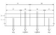
도 1은 본 발명의 바람직한 일 실시예에 따른 유기 발광 표시 장치를 개략적으로 도시한 단면도이다.FIG. 1 is a cross-sectional view schematically showing an organic light emitting diode display according to a preferred embodiment of the present invention. Referring to FIG.
도 1을 참조하면, 본 발명의 바람직한 일 실시예에 따른 유기 발광 표시 장치는 기판(1) 상에 디스플레이부(2)가 구비된다.Referring to FIG. 1, an OLED display according to an embodiment of the present invention includes a
이러한 유기 발광 표시 장치에서 외광은 기판(1) 및 디스플레이부(2)를 투과하여 입사된다.In such an OLED display, external light is transmitted through the
그리고 디스플레이부(2)는 후술하는 바와 같이 외광이 투과 가능하도록 구비된 것으로, 도 1에서 볼 때, 화상이 구현되는 측에 위치한 사용자가 디스플레이부(2) 외측의 이미지를 관찰 가능하도록 구비된다.As shown in FIG. 1, the
도 1은 본 발명의 유기 발광 표시 장치의 서로 인접한 두 개의 단위 픽셀들인 제1 픽셀(P1)과 제2 픽셀(P2)을 도시한 것으로, 각 단위 픽셀들(P1)(P2)은 제1 영역(31)과 제2 영역(32)을 구비하고 있다.FIG. 1 shows a first pixel P1 and a second pixel P2 which are two unit pixels adjacent to each other in the organic light emitting display according to the present invention. Each unit pixel P1 and P2 includes a first region P1, (31) and a second region (32).
각 단위 픽셀들(P1)(P2)의 제1 영역(31)을 통해서는 디스플레이부(2)로부터 화상이 구현되고, 제2 영역(32)을 통해서는 외광이 투과된다.An image is realized from the
즉, 본 발명은 각 단위 픽셀들(P1)(P2)이 모두 화상을 구현하는 제1 영역(31)과 외광이 투과되는 제2 영역(32)이 구비되어 사용자가 화상에서 구현되는 이미지를 보지 않고자 할 때에는 외부 이미지를 볼 수 있게 된다.That is, according to the present invention, a
이때, 제2 영역(32)은 박막 트랜지스터, 커패시터, 유기 발광 소자 등의 소자들을 형성하지 않음으로써 외광 투과율을 극대화할 수 있고, 투과 이미지가 박막 트랜지스터, 커패시터, 유기 발광 소자 등의 소자들에 의해 간섭을 받아 왜곡이 일어나는 것을 최대한 줄일 수 있다.At this time, since the
한편, 본 실시예에서 각 단위 픽셀들(P1)(P2)에 형성된 제1 영역(31)과 제2 영역(32)은 서로 인접하는 단위 픽셀들(P1)(P2) 간에 서로 대칭적으로 형성된다.The
특히, 외광이 투과되는 각 단위 픽셀들(P1)(P2)에 형성된 제2 영역(32)은 서로 연결되도록 형성된다.In particular, the
따라서, 외광이 투과되는 제2 영역(32)이 각 단위 픽셀들(P1)(P2) 간에 연결되어 제2 영역(32)의 면적이 증가되므로, 외광 투과율을 극대화할 수 있고 투과 이미지의 왜곡을 더욱 줄일 수 있다.Accordingly, since the
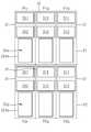
도 2는 적색(P1r)(P2r), 녹색(P1g)(P2g) 및 청색(P1b)(P2b)의 서브 픽셀들을 구비한 서로 인접한 단위 픽셀들(P1)(P2)을 도시한 평면도이다.2 is a plan view showing mutually adjacent unit pixels P1 (P2) with subpixels of red (P1r), P2r, green (P1g), and blue (P1b)
제1 단위 픽셀(P1)은 적색의 서브 픽셀(P1r), 녹색의 서브 픽셀(P1g) 및 청색의 서브 픽셀(P1b)을 구비하고, 각 적색의 서브 픽셀(P1r), 녹색의 서브 픽셀(P1g) 및 청색의 서브 픽셀(P1b)은 제1 영역(31)에 회로 영역(311)과 발광 영역(312)를 구비한다. 이들 회로 영역(311)과 발광 영역(312)은 서로 인접하게 배치된다.The first unit pixel P1 includes a red subpixel P1r, a green subpixel P1g and a blue subpixel P1b, and each red subpixel P1r, green subpixel P1g And the blue subpixel P1b have a
제2 단위 픽셀(P2)은 적색의 서브 픽셀(P2r), 녹색의 서브 픽셀(P2g) 및 청색의 서브 픽셀(P2b)을 구비하고, 각 적색의 서브 픽셀(P2r), 녹색의 서브 픽셀(P2g) 및 청색의 서브 픽셀(P2b)은 제1 영역(31)에 회로 영역(311)과 발광 영역(312)를 구비한다. 이들 회로 영역(311)과 발광 영역(312)은 서로 인접하게 배치된다.The second unit pixel P2 includes a red subpixel P2r, a green subpixel P2g and a blue subpixel P2b, and each red subpixel P2r, green subpixel P2g And the blue subpixel P2b have a
그리고, 제1 영역(31)과 제2 영역(32)은 제1 단위 픽셀(P1)과 제2 단위 픽셀(P2) 간에 대칭적으로 형성된다. 즉, 제1 영역(31)과 제2 영역(32)은 L1을 기준으로 대칭적으로 형성된다.The
그 결과, 제2 영역(32)은 제1 단위 픽셀(P1)과 제2 단위 픽셀(P2)에 걸쳐서 연속적으로 배치되어, 외광이 투과되는 제2 영역(32)의 면적이 증가된다.As a result, the
반면, 본 발명의 비교예인 도 4에 도시된 유기 발광 표시 장치에서는 제2 영역(32)이 각 서브 픽셀별(P1r)(P2r)(P1g)(P2g)(P1b)(P2b)로 독립되게 구비되거나, 도 5에 도시된 유기 발광 표시 장치에서는 제2 영역(32)이 각 단위 픽셀별(P1)(P2)로 독립되게 구비된다.In contrast, in the organic light emitting display shown in FIG. 4, which is a comparative example of the present invention, the
따라서, 본 발명에 따른 유기 발광 표시 장치는 상기 도 4 및 도 5에 도시된 유기 발광 표시 장치에 비하여, 외광이 투과하는 영역의 면적을 극대화할 수 있으므로, 외광 투과율을 극대화할 수 있고 투과 이미지의 왜곡을 더욱 줄일 수 있다.Therefore, the organic light emitting display according to the present invention can maximize the area of the region through which the external light is transmitted as compared with the organic light emitting display shown in FIGS. 4 and 5, thereby maximizing the external light transmittance, Distortion can be further reduced.
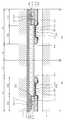
도 3은 도 1 및 도 2에 도시된 인접한 두 단위 픽셀들(P1)(P2)의 단면을 도시한 것이다.Fig. 3 shows a cross section of two adjacent unit pixels P1 (P2) shown in Figs. 1 and 2.
도 3을 참조하면, 각 단위 픽셀들(P1)(P2)의 회로 영역(311)에는 박막 트랜지스터(TR1)(TR2)가 배치되는데, 도면에 도시된 바와 같이 각 단위 픽셀(P1)(P1)에는 반드시 하나의 박막 트랜지스터(TR1)(TR2)가 배치되는 것에 한정되지 않으며, 이 박막 트랜지스터(TR1)(TR2)를 포함한 픽셀 회로가 구비될 수 있다.Referring to FIG. 3, thin film transistors TR1 and TR2 are disposed in a
이 픽셀 회로에는 박막 트랜지스터(TR1)(TR2) 외에도 다수의 박막 트랜지스터 및 스토리지 커패시터가 더 포함될 수 있으며, 이들과 연결된 스캔 라인, 데이터 라인 및 Vdd 라인 등의 배선이 더 구비될 수 있다. 여기서, 스캔 라인, 데이터 라인 및 Vdd 라인 등의 배선은 외광이 투과되는 제2 영역(32) 외곽에 배치되는 것이 바람직하다.In addition to the thin film transistors TR1 and TR2, a plurality of thin film transistors and storage capacitors may be further included in the pixel circuit, and wirings such as a scan line, a data line, and a Vdd line may be further provided. Here, the wirings such as the scan line, the data line, and the Vdd line are preferably disposed outside the
각 단위 픽셀들(P1)(P2)의 발광 영역(312)에는 발광 소자인 유기 발광 소자(EL1)(EL2)가 배치된다. 각 유기 발광 소자(EL1)(EL2)는 픽셀 회로의 박막 트랜지스터(TR1)(TR2)와 전기적으로 연결되어 있다.The organic light emitting elements EL1 and EL2 as light emitting elements are disposed in the
상기 기판(1) 상에는 버퍼막(211)이 형성되고, 이 버퍼막(211) 상에 박막 트랜지스터(TR1)(TR2)를 포함한 픽셀 회로가 형성된다.A
먼저, 상기 버퍼막(211) 상에는 반도체 활성층(212)이 형성된다.First, a semiconductor
상기 버퍼막(211)은 불순 원소의 침투를 방지하며 표면을 평탄화하는 역할을 하는 것으로, 이러한 역할을 수행할 수 있는 다양한 물질로 형성될 수 있다. 일례로, 상기 버퍼막(211)은 실리콘 옥사이드, 실리콘 나이트라이드, 실리콘 옥시나이트라이드, 알루미늄옥사이드, 알루미늄나이트라이드, 티타늄옥사이드 또는 티타늄나이트라이드 등의 무기물이나, 폴리이미드, 폴리에스테르, 아크릴 등의 유기물 또는 이들의 적층체로 형성될 수 있다. 상기 버퍼막(211)은 필수 구성요소는 아니며, 필요에 따라 구비되지 않을 수 있다.The
상기 반도체 활성층(212)은 다결정 실리콘으로 형성될 수 있는 데, 반드시 이에 한정되는 것은 아니며, 산화물 반도체로 형성될 수 있다. 예를 들면 G-I-Z-O층[(In2O3)a(Ga2O3)b(ZnO)c층](a, b, c는 각각 a≥0, b≥0, c>0의 조건을 만족시키는 실수)일 수 있다. 이렇게 반도체 활성층(212)을 산화물 반도체로 형성할 경우에는 광투과도가 더욱 높아질 수 있게 되고, 이에 따라 디스플레이부(2) 전체의 외광 투과도를 상승시킬 수 있다.The semiconductor
상기 반도체 활성층(212)을 덮도록 게이트 절연막(213)이 버퍼막(211) 상에 형성되고, 게이트 절연막(213) 상에 게이트 전극(214)이 형성된다.A
게이트 전극(214)을 덮도록 게이트 절연막(213) 상에 층간 절연막(215)이 형성되고, 이 층간 절연막(215) 상에 소스 전극(216)과 드레인 전극(217)이 형성되어 각각 반도체 활성층(212)과 콘택 홀을 통해 콘택된다.An interlayer insulating
상기와 같은 박막 트랜지스터(TR1)(TR2)의 구조는 반드시 이에 한정되는 것은 아니며, 다양한 형태의 박막 트랜지스터의 구조가 적용 가능함은 물론이다.The structures of the thin film transistors TR1 and TR2 are not limited thereto, and various structures of thin film transistors may be applied.
이러한 박막 트랜지스터(TR1)(TR2)를 덮도록 패시베이션막(218)이 형성된다. 상기 패시베이션막(218)은 상면이 평탄화된 단일 또는 복수층의 절연막이 될 수 있다. 이 패시베이션막(218)은 무기물 및/또는 유기물로 형성될 수 있다.A
상기 패시베이션막(218) 상에는 제1 단위 픽셀(P1) 및 제2 단위 픽셀(P2)에 배치된 박막 트랜지스터(TR1)(TR2)와 전기적으로 연결된 유기 발광 소자(EL1)(EL2)의 제1 전극(221)이 각각 형성된다. 상기 제1 전극(221)은 모든 서브 픽셀별로 독립된 아일랜드 형태로 형성된다.A first electrode of the organic light emitting device EL1 EL2 electrically connected to the thin film transistors TR1 and TR2 arranged in the first unit pixel P1 and the second unit pixel P2 is formed on the
상기 패시베이션막(218) 상에는 유기 및/또는 무기 절연물로 구비된 화소 정의막(219)이 형성된다.On the
상기 화소 정의막(219)은, 상기 제1 전극(221)의 가장자리를 덮고 중앙부는 노출시킨다. 이 화소 정의막(219)은 제1 영역(31)을 덮도록 구비될 수 있는데, 반드시 제1 영역(31) 전체를 덮도록 구비되는 것은 아니며, 적어도 일부, 특히 제1 전극(221)의 가장자리를 덮도록 하면 충분하다.The
도 3을 참조하면, 본 실시예에 따른 화소 정의막(219)은 각 단위 픽셀(P1)(P2)의 제2 영역(32)에 대응되는 개구를 갖는 것을 알 수 있다. 즉, 상기 화소 정의막(219)의 개구는 인접하는 두 개의 단위 픽셀들(P1)(P2)에 대해 서로 연결되어 형성될 수 있다. 이 개구는 후술하겠지만 제2 전극(222)에 형성된 투과창(224)에 대응되도록 형성될 수 있다. 한편, 본 실시예에서는 화소 정의막(219)이 제2영역(32)에 대응되는 개구를 갖도록 형성되었지만, 본 발명은 이에 한정되지 않는다. 즉, 화소 정의막(219)이 소정의 투과도를 가지는 경우에 개구를 형성하지 않을 수 있으며, 제2영역(32)에 대응되는 영역에 음각을 형성하여 제2영역(32)에 대응되는 영역을 얇게 형성할 수도 있다.Referring to FIG. 3, it is understood that the
상기 제1 전극(221) 상에는 유기막(223)과 제2 전극(222)이 순차로 적층된다. 상기 제2 전극(222)은 유기막(223)과 화소 정의막(219)을 덮으며, 모든 픽셀들에 걸쳐서 서로 전기적으로 연결되어 있다.An
상기 유기막(223)은 저분자 또는 고분자 유기막이 사용될 수 있다. 저분자 유기막을 사용할 경우, 홀 주입층(HIL: Hole Injection Layer), 홀 수송층(HTL: Hole Transport Layer), 발광층(EML: Emission Layer), 전자 수송층(ETL: Electron Transport Layer), 전자 주입층(EIL: Electron Injection Layer) 등이 단일 혹은 복합의 구조로 적층되어 형성될 수 있으며, 사용 가능한 유기 재료도 구리 프탈로시아닌(CuPc: copper phthalocyanine), N,N-디(나프탈렌-1-일)-N,N'-디페닐-벤지딘 (N,N'-Di(naphthalene-1-yl)-N,N'-diphenyl-benzidine: NPB) , 트리스-8-하이드록시퀴놀린 알루미늄(tris-8-hydroxyquinoline aluminum)(Alq3) 등을 비롯해 다양하게 적용 가능하다. 이들 저분자 유기막은 진공증착의 방법 등으로 형성될 수 있다. 이때, 상기 발광층은 적, 녹, 청색의 화소마다 독립되게 형성되고, 홀 주입층, 홀 수송층, 전자 수송층, 및 전자 주입층 등은 공통층으로서, 적, 녹, 청색의 화소에 공통으로 적용될 수 있다.The
상기 제1 전극(221)은 애노드 전극의 기능을 하고, 상기 제2 전극(222)은 캐소드 전극의 기능을 할 수 있는데, 물론 이들 제1 전극(221) 및 제2 전극(222)의 극성은 서로 반대로 되어도 무방하다.The
본 발명의 일 실시예에 따르면, 상기 제1 전극(221)은 투명 전극이 될 수 있고, 상기 제2 전극(222)은 반사 전극이 될 수 있다. 상기 제1 전극(221)은 일함수가 높은 ITO, IZO, ZnO, 또는 In2O3 등을 포함하여 구비될 수 있다. 그리고 상기 제2 전극(222)은 일함수가 작은 금속, 즉, Ag, Mg, Al, Pt, Pd, Au, Ni, Nd, Ir, Cr, Li, Ca 또는 이들의 합금으로 형성될 수 있다. 따라서, 본 실시예에 따른 유기 발광 소자(EL1)(EL2)는 제1 전극(221) 방향으로 화상을 구현하는 배면 발광형(bottom emission type)이 된다.According to an embodiment of the present invention, the
그러나 본 발명은 반드시 이에 한정되는 것은 아니며, 상기 제1전극(221)이 반사 전극, 상기 제2 전극(222)이 투명 전극으로 구비될 수 있다.However, the present invention is not limited thereto, and the
패시베이션막(218)은 투명한 절연막으로 형성하는 것이 바람직하다. 패시베이션막(218)이 투명할 경우, 도 3에 도시된 바와 같이, 제2영역(32)에 대응되는 부부에 별도의 개구를 형성할 필요는 없다. 그러나, 본 발명은 반드시 이에 한정되는 것은 아니며, 외광 투과 효과를 높이기 위하여 제2영역(32)에 대응되는 영역의 패시베이션막(218)에 개구를 형성할 수 있으며, 이때, 패시베이션막(218)은 투과도가 낮은 재료로 구비될 수도 있다.The
버퍼막(211), 게이트 절연막(213), 및 층간 절연막(215)은 투명한 절연막으로 형성하는 것이 바람직하다. 그러나, 본 발명은 이에 한정되는 것은 아니며, 전술한 패시베이션막(218)과 마찬가지로, 외광 투과 효과를 높이기 위하여 제2영역(32)에 대응되는 영역에 개구를 형성할 수 있으며, 이때, 버퍼막(211), 게이트 절연막(213), 및 층간 절연막(215)은 투과도가 낮은 재료로 구비될 수도 있다.The
상기 제2 전극(222) 상부에는 밀봉 기판(4)이 배치될 수 있다. 이 밀봉 기판(4)은 디스플레이부(2) 외곽에서 별도의 실런트(미도시)에 의해 기판(1)과 접합되어 디스플레이부(2)를 외기에 대해 밀봉하도록 할 수 있다.A sealing
밀봉 기판(4)과 제2 전극(222) 사이 공간에는 별도의 충진재(미도시)가 충진될 수 있고, 흡습제도 개재될 수 있다. 디스플레이부(2)에 대한 밀봉 구조는 반드시 밀봉 기판(4)을 사용하는 것에 한정되는 것은 아니며, 필름 형태의 밀봉 구조도 적용 가능하다.(Not shown) may be filled in the space between the sealing
한편, 본 실시예에 있어서, 상기 제2 전극(222) 및 화소 정의막(219)에는 투과창(224)이 더 형성될 수 있다.Meanwhile, in this embodiment, a
그러나, 본 발명은 이에 한정되는 것은 아니며, 제2영역(32)이 외광을 투과할 수 있는 한, 전술한 바와 같이 제2 전극(222)을 투명 재료로 얇게 형성하는 경우에는 제2 전극(222)에 투과 창을 형성하기 위한 별도의 패터닝을 하지 않을 수 있으며, 투명한 제2전극(222)을 소정 두께로 형성한 경우, 투과창(224) 영역에 대응되는 부분을 음각으로 패터닝하여 얇게 형성할 수도 있다.However, the present invention is not limited thereto. When the
투과 창(224)은 각 단위 픽셀(P1)(P2)의 제2 영역(32)에 대응되는 위치에 형성된다. 본 실시예에서 투과 창(224)은 도 2에 도시된 것과 같이 제2전극 및 화소정의막이 개구된 형태로 형성될 수 있다. 즉, 인접하는 제1 단위 픽셀(P1) 및 제2 단위 픽셀(P2)에 대해 연결되어 형성될 수 있다. 따라서, 외광이 투과하는 영역의 면적 및 외광 투과율을 더욱 높여 투과 이미지의 왜곡을 더욱 줄일 수 있다.The
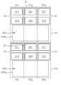
도 6은 본 발명의 바람직한 다른 일 실시예에 따른 유기 발광 표시 장치의 개략적인 평면도로, 네 개의 단위 픽셀들(P1)(P2)(P3)(P4)을 도시한 평면도이다.FIG. 6 is a schematic plan view of an organic light emitting display according to another embodiment of the present invention, and is a plan view showing four unit pixels P1, P2, P3, and P4.
제1 내지 제4 단위 픽셀(P1)(P2)(P3)(P4)은 각각 적색의 서브 픽셀(P1r)(P2r)(P3r)(P4r), 녹색의 서브 픽셀(P1g)(P2g)(P3g)(P4g) 및 청색의 서브 픽셀(P1b)(P2b)(P3b)(P4b)을 구비하고, 각 적색의 서브 픽셀(P1r)(P2r)(P3r)(P4r), 녹색의 서브 픽셀(P1g)(P2g)(P3g)(P4g) 및 청색의 서브 픽셀(P1b)(P2b)(P3b)(P4b)은 제1 영역(31)에 회로 영역(311)과 발광 영역(312)를 구비한다. 이들 회로 영역(311)과 발광 영역(312)은 서로 인접하게 배치된다.The first through fourth unit pixels P1, P2, P3 and P4 are red subpixels P1r, P2r, P3r, P4r, green subpixels P1g, P2g, P3g, ) P4g and blue subpixels P1b and P2b and P3b and P4b and the red subpixels P1r, P2r, P3r and P4r, the green subpixel P1g, The first sub-pixel P2g, the third sub-pixel P3g and the blue sub-pixels P1b, P2b, P3b and P4b have a
그리고, 제1 영역(31) 및 제2 영역(32)은 각 단위 픽셀들(P1)(P2)(P3)(P4) 간에 대칭적으로 형성된다. 즉, 제1 영역(31)과 제2 영역(32)은 L1 및 L2에 대하여 대칭적으로 형성된다.The
그 결과, 제2 영역(32)은 네 개의 단위 픽셀(P1)(P2)(P3)(P4)에 걸쳐서 연속적으로 배치되어, 외광이 투과되는 제2 영역(32)의 면적이 전술한 실시예에 따른 유기 발광 표시 장치보다 두 배로 증가된다.As a result, the
따라서, 본 실시예에 따른 유기 발광 표시 장치는 외광이 투과하는 영역의 면적을 극대화할 수 있으므로, 외광 투과율을 극대화할 수 있고 투과 이미지의 왜곡을 더욱 줄일 수 있다.Therefore, the organic light emitting display according to the present embodiment can maximize the area of the region through which the external light is transmitted, thereby maximizing the external light transmittance and further reducing the distortion of the transmitted image.
이상 설명한 본 발명은 도 3에서와 같이 박막 트랜지스터(TR1)(TR2)를 포함한 회로부가 제1 전극(221)과 중첩되지 않는 구조에만 적용되는 것은 아니며, 도 7에서 볼 수 있듯이. 박막 트랜지스터(TR1)(TR2)를 포함한 회로부가 제1 전극(221)과 중첩되는 구조에도 적용될 수 있다.3, the present invention is not limited to the structure in which the circuit portion including the thin film transistors TR1 and TR2 does not overlap with the
도 7과 같은 구조의 경우, 제1 전극(221)을 반사 전극으로 형성하면 제1 전극(221)에 의해 회로부의 도전 패턴이 가리워지는 효과를 얻을 수 있기 때문에 외광이 회로부의 도전 패턴에 의해 산란되어 투과 이미지 왜곡이 발생하는 것을 줄 일수 있다.7, when the
한편, 상기 도면들에 도시된 구성요소들은 설명의 편의상 확대 또는 축소되어 표시될 수 있으므로, 도면에 도시된 구성요소들의 크기나 형상에 본 발명이 구속되는 것은 아니며, 본 기술 분야의 통상의 지식을 가진 자라면 이로부터 다양한 변형 및 균등한 다른 실시예가 가능하다는 점을 이해할 것이다. 따라서 본 발명의 진정한 기술적 보호범위는 첨부된 특허청구범위의 기술적 사상에 의하여 정해져야 할 것이다.It is to be understood that both the foregoing general description and the following detailed description are exemplary and explanatory and are not restrictive of the invention, Those skilled in the art will appreciate that various modifications and equivalent embodiments are possible. Accordingly, the true scope of the present invention should be determined by the technical idea of the appended claims.
1: 기판2: 디스플레이부
4: 밀봉 기판31: 제1 영역
32: 제2 영역211: 버퍼막
212: 반도체 활성층213: 게이트 절연막
214: 게이트 전극215: 층간 절연막
216: 소스 전극217: 드레인 전극
218: 패시베이션막219: 화소 정의막
221: 제1 전극222: 제2 전극
223: 유기막224: 투과 창
311: 회로 영역312: 발광 영역
P1~P4: 단위 픽셀1: substrate 2: display portion
4: sealing substrate 31: first region
32: second region 211: buffer film
212: semiconductor active layer 213: gate insulating film
214: gate electrode 215: interlayer insulating film
216: source electrode 217: drain electrode
218: passivation film 219: pixel defining film
221: first electrode 222: second electrode
223: Organic film 224: Transmission window
311: Circuit area 312: Light emitting area
P1 to P4: unit pixel
Claims (18)
Translated fromKorean상기 기판 상에 형성되고, 발광되는 제1 영역과 외광이 투과되는 제2 영역을 포함하는 복수의 서브 픽셀;
상기 복수의 서브 픽셀의 제1 영역에 배치되는 복수의 박막 트랜지스터와 상기 박막 트랜지스터와 전기적으로 연결된 배선부;
상기 복수의 서브 픽셀의 제1 영역에 배치되고 상기 각 박막 트랜지스터와 전기적으로 연결되고 광반사 물질을 포함하는 복수의 제1 전극;
상기 제1 전극에 대향되고 상기 복수의 서브 픽셀에 공통으로 배치되고 광투과 물질을 포함하는 제2 전극;
상기 제1 전극과 제2 전극 사이에 개재되고 발광층을 포함하는 유기막; 및
상기 제1 전극의 가장자리를 덮는 화소 정의막;을 포함하고,
상기 복수의 서브 픽셀의 상기 발광층의 서로 다른 발광색을 최소 단위로 포함하는 복수의 단위 픽셀을 포함하고,
상기 외광이 투과하는 제2 영역은 서브 픽셀 간 및 단위 픽셀 간에 공유되고,
상기 화소 정의막은 상기 서브 픽셀 간 및 상기 단위 픽셀 간에 공유되는 개구를 가지고,
상기 박막 트랜지스터, 상기 제1 전극, 상기 배선부 및 상기 화소 정의막은 상기 제2 영역과 중첩되지 않는 유기 발광 표시 장치.Board;
A plurality of subpixels formed on the substrate and including a first region that emits light and a second region that transmits external light;
A plurality of thin film transistors arranged in a first region of the plurality of subpixels and a wiring portion electrically connected to the thin film transistors;
A plurality of first electrodes disposed in a first region of the plurality of subpixels and electrically connected to the respective thin film transistors and including a light reflecting material;
A second electrode opposing the first electrode and disposed in common to the plurality of subpixels and including a light transmissive material;
An organic layer interposed between the first electrode and the second electrode and including a light emitting layer; And
And a pixel defining layer covering an edge of the first electrode,
A plurality of unit pixels including a plurality of different emission colors of the emission layers of the plurality of subpixels as a minimum unit,
The second region through which the external light passes is shared between the sub-pixels and between the unit pixels,
Wherein the pixel defining layer has an opening shared between the sub-pixels and the unit pixel,
Wherein the thin film transistor, the first electrode, the wiring portion, and the pixel defining layer are not overlapped with the second region.
상기 제1 영역과 제2 영역은 서로 인접하는 두 개의 단위 픽셀 간에 서로 대칭되도록 형성되는 것을 특징으로 하는 유기 발광 표시 장치.The method according to claim 1,
Wherein the first region and the second region are formed to be symmetrical to each other between two unit pixels adjacent to each other.
상기 제1 영역과 제2 영역은 서로 인접하는 네 개의 단위 픽셀 간에 서로 대칭되도록 형성되는 것을 특징으로 하는 유기 발광 표시 장치.The method according to claim 1,
Wherein the first region and the second region are formed to be symmetrical to each other between four unit pixels adjacent to each other.
상기 제2 전극은 상기 제2 영역에 대응되는 부분이 개구된 형태의 투과 창을 갖는 것을 특징으로 하는 유기 발광 표시 장치.The method according to claim 1,
And the second electrode has a transmission window in which a portion corresponding to the second region is opened.
상기 투과창은 서로 인접하는 두 개의 단위 픽셀들에 대해 연결되도록 형성된 것을 특징으로 하는 유기 발광 표시 장치.5. The method of claim 4,
Wherein the transmissive window is formed to be connected to two unit pixels adjacent to each other.
상기 투과창은 서로 인접하는 네 개의 단위 픽셀들에 대해 연결되도록 형성된 것을 특징으로 하는 유기 발광 표시 장치.5. The method of claim 4,
Wherein the transmissive window is formed to be connected to four unit pixels adjacent to each other.
상기 박막 트랜지스터는 상기 제1 전극에 중첩된 것을 특징으로 하는 유기 발광 표시 장치.The method according to claim 1,
Wherein the thin film transistor is overlapped with the first electrode.
상기 복수의 서브 픽셀의 제1 영역은 발광 영역과 회로 영역을 포함하고, 상기 박막 트랜지스터는 상기 회로 영역에 배치되며, 상기 제1 전극은 상기 발광 영역에 배치되는 것을 특징으로 하는 유기 발광 표시 장치.The method according to claim 1,
Wherein the first region of the plurality of subpixels includes a light emitting region and a circuit region, the thin film transistor is disposed in the circuit region, and the first electrode is disposed in the light emitting region.
상기 복수의 서브 픽셀의 상기 발광 영역과 상기 회로 영역은 서로 인접하게 배치되는 것을 특징으로 하는 유기 발광 표시 장치.9. The method of claim 8,
Wherein the light emitting region and the circuit region of the plurality of subpixels are disposed adjacent to each other.
상기 배선부는 상기 발광 영역과 상기 회로 영역을 전기적으로 연결하고,
상기 배선부는 상기 제2 영역 외곽에 배치되는 것을 특징으로 하는 유기 발광 표시 장치.9. The method of claim 8,
Wherein the wiring portion electrically connects the light emitting region and the circuit region,
And the wiring portion is disposed outside the second region.
상기 복수의 박막 트랜지스터를 덮는 패시베이션막을 더 포함하고,
상기 화소 정의막은 상기 패시베이션막 상에 형성된 것을 특징으로 하는 유기 발광 표시 장치.The method according to claim 1,
Further comprising a passivation film covering the plurality of thin film transistors,
Wherein the pixel defining layer is formed on the passivation layer.
상기 화소 정의막은 상기 제2 영역에 대응되도록 개구를 갖는 것을 특징으로 하는 유기 발광 표시 장치.12. The method of claim 11,
Wherein the pixel defining layer has an opening corresponding to the second region.
상기 화소 정의막의 개구는 서로 인접하는 두 개의 단위 픽셀들에 대해 연결되도록 형성된 것을 특징으로 하는 유기 발광 표시 장치.13. The method of claim 12,
Wherein the opening of the pixel defining layer is formed to be connected to two unit pixels adjacent to each other.
상기 화소 정의막의 개구는 서로 인접하는 네 개의 단위 픽셀들에 대해 연결되도록 형성된 것을 특징으로 하는 유기 발광 표시 장치.13. The method of claim 12,
Wherein an opening of the pixel defining layer is formed to be connected to four unit pixels adjacent to each other.
상기 패시베이션막은 상기 제2 영역에 대응되도록 개구를 갖는 것을 특징으로 하는 유기 발광 표시 장치.12. The method of claim 11,
Wherein the passivation film has openings corresponding to the second regions.
상기 기판 상에 버퍼층이 더 포함된 것을 특징으로 하는 유기 발광 표시 장치.The method according to claim 1,
And a buffer layer is further formed on the substrate.
상기 버퍼층은 상기 제2 영역에 대응되도록 개구를 갖는 것을 특징으로 하는 유기 발광 표시 장치.17. The method of claim 16,
And the buffer layer has an opening corresponding to the second region.
상기 기판 상에 형성되고, 서로 다른 색을 발광하는 복수의 서브 픽셀;
상기 복수의 서브 픽셀의 서로 다른 발광색을 최소 단위로 포함하는 복수의 단위픽셀;을 포함하고,
하나의 단위 픽셀에 포함된 복수의 서브 픽셀은,
각 서브 픽셀마다 위치하는 발광 영역과, 상기 발광 영역에 연결된 적어도 하나의 박막 트랜지스터를 구비한 회로 영역을 포함하는 제1영역,
상기 발광 영역의 가장자리를 덮는 화소 정의막; 및
상기 하나의 단위 픽셀에 포함된 복수의 서브 픽셀 간에 공유된 화소 정의막에 형성된 개구를 갖는, 외광이 투과되는 제2영역을 포함하고,
상기 제2영역은 서로 인접한 단위 픽셀 간에도 공유되는 상기 화소 정의막의 개구를 가지고,
상기 발광 영역과 회로 영역을 연결하는 배선부는 상기 제2영역 외곽에 배치되는 유기 발광 표시 장치.
Board;
A plurality of subpixels formed on the substrate and emitting different colors;
A plurality of unit pixels including a plurality of different emission colors of the plurality of subpixels as a minimum unit,
A plurality of subpixels included in one unit pixel,
A first region including a light emitting region located for each sub-pixel, and a circuit region including at least one thin film transistor connected to the light emitting region,
A pixel defining layer covering an edge of the light emitting region; And
And a second region through which external light is transmitted, the second region having an opening formed in a pixel defining film shared between a plurality of subpixels included in the one unit pixel,
The second region having an opening in the pixel defining layer that is also shared between adjacent unit pixels,
And a wiring portion connecting the light emitting region and the circuit region is disposed outside the second region.
Priority Applications (1)
| Application Number | Priority Date | Filing Date | Title |
|---|---|---|---|
| KR1020170167765AKR101918751B1 (en) | 2017-12-07 | 2017-12-07 | Organic light emitting display device |
Applications Claiming Priority (1)
| Application Number | Priority Date | Filing Date | Title |
|---|---|---|---|
| KR1020170167765AKR101918751B1 (en) | 2017-12-07 | 2017-12-07 | Organic light emitting display device |
Related Parent Applications (1)
| Application Number | Title | Priority Date | Filing Date |
|---|---|---|---|
| KR1020100096513ADivisionKR20120035039A (en) | 2010-10-04 | 2010-10-04 | Organic light emitting display |
Publications (2)
| Publication Number | Publication Date |
|---|---|
| KR20170140136A KR20170140136A (en) | 2017-12-20 |
| KR101918751B1true KR101918751B1 (en) | 2019-02-11 |
Family
ID=60931696
Family Applications (1)
| Application Number | Title | Priority Date | Filing Date |
|---|---|---|---|
| KR1020170167765AActiveKR101918751B1 (en) | 2017-12-07 | 2017-12-07 | Organic light emitting display device |
Country Status (1)
| Country | Link |
|---|---|
| KR (1) | KR101918751B1 (en) |
Cited By (1)
| Publication number | Priority date | Publication date | Assignee | Title |
|---|---|---|---|---|
| US11569316B2 (en) | 2020-01-22 | 2023-01-31 | Samsung Display Co., Ltd. | Display device |
Families Citing this family (3)
| Publication number | Priority date | Publication date | Assignee | Title |
|---|---|---|---|---|
| CN110021640B (en) | 2018-01-08 | 2025-02-11 | 三星显示有限公司 | Electroluminescent device |
| KR20210002232A (en) | 2019-06-28 | 2021-01-07 | 삼성디스플레이 주식회사 | Display panel and display device |
| KR102669163B1 (en)* | 2019-07-12 | 2024-05-28 | 삼성디스플레이 주식회사 | Pixel, display device including the same and method of fabricating the display device |
Citations (2)
| Publication number | Priority date | Publication date | Assignee | Title |
|---|---|---|---|---|
| JP2006128241A (en)* | 2004-10-27 | 2006-05-18 | Seiko Epson Corp | Display device and electronic device |
| JP2008112112A (en)* | 2006-10-31 | 2008-05-15 | Optrex Corp | Light emitting device |
- 2017
- 2017-12-07KRKR1020170167765Apatent/KR101918751B1/enactiveActive
Patent Citations (2)
| Publication number | Priority date | Publication date | Assignee | Title |
|---|---|---|---|---|
| JP2006128241A (en)* | 2004-10-27 | 2006-05-18 | Seiko Epson Corp | Display device and electronic device |
| JP2008112112A (en)* | 2006-10-31 | 2008-05-15 | Optrex Corp | Light emitting device |
Cited By (3)
| Publication number | Priority date | Publication date | Assignee | Title |
|---|---|---|---|---|
| US11569316B2 (en) | 2020-01-22 | 2023-01-31 | Samsung Display Co., Ltd. | Display device |
| US11812641B2 (en) | 2020-01-22 | 2023-11-07 | Samsung Display Co., Ltd. | Display device |
| US12161023B2 (en) | 2020-01-22 | 2024-12-03 | Samsung Display Co., Ltd. | Display device |
Also Published As
| Publication number | Publication date |
|---|---|
| KR20170140136A (en) | 2017-12-20 |
Similar Documents
| Publication | Publication Date | Title |
|---|---|---|
| KR101097338B1 (en) | Organic light emitting display | |
| KR101156435B1 (en) | Organic light emitting display device | |
| KR101084189B1 (en) | Organic light emitting display | |
| KR20120035039A (en) | Organic light emitting display | |
| US8797239B2 (en) | Organic light-emitting display device | |
| KR101146984B1 (en) | Organic light emitting display device | |
| KR101146988B1 (en) | Organic light emitting display device | |
| KR101223722B1 (en) | Organic light emitting display device | |
| KR101923173B1 (en) | Organic light emitting display device | |
| US8421342B2 (en) | Organic light-emitting display device | |
| US9099674B2 (en) | Organic light-emitting display device | |
| JP5687865B2 (en) | Organic light-emitting display device and method for manufacturing the same | |
| US8664848B2 (en) | Organic light emitting display device | |
| KR101223727B1 (en) | Organic light emitting display device and manufacturing method thereof | |
| KR101097346B1 (en) | Organic light emitting display device | |
| KR20120019026A (en) | Organic light emitting display device | |
| US11903267B2 (en) | Organic light-emitting display apparatus | |
| KR20120124222A (en) | Organic light emitting display device | |
| JP2012015092A (en) | Organic light emitting display device | |
| KR20120019025A (en) | Organic light emitting display device | |
| KR101918751B1 (en) | Organic light emitting display device | |
| KR101801912B1 (en) | Organic light emitting display device |
Legal Events
| Date | Code | Title | Description |
|---|---|---|---|
| A107 | Divisional application of patent | ||
| A201 | Request for examination | ||
| PA0107 | Divisional application | Comment text:Divisional Application of Patent Patent event date:20171207 Patent event code:PA01071R01D Filing date:20101004 Application number text:1020100096513 | |
| PA0201 | Request for examination | ||
| PG1501 | Laying open of application | ||
| E902 | Notification of reason for refusal | ||
| PE0902 | Notice of grounds for rejection | Comment text:Notification of reason for refusal Patent event date:20180207 Patent event code:PE09021S01D | |
| E701 | Decision to grant or registration of patent right | ||
| PE0701 | Decision of registration | Patent event code:PE07011S01D Comment text:Decision to Grant Registration Patent event date:20180906 | |
| GRNT | Written decision to grant | ||
| PR0701 | Registration of establishment | Comment text:Registration of Establishment Patent event date:20181108 Patent event code:PR07011E01D | |
| PR1002 | Payment of registration fee | Payment date:20181109 End annual number:3 Start annual number:1 | |
| PG1601 | Publication of registration | ||
| PR1001 | Payment of annual fee | Payment date:20211027 Start annual number:4 End annual number:4 | |
| PR1001 | Payment of annual fee | Payment date:20221025 Start annual number:5 End annual number:5 | |
| PR1001 | Payment of annual fee | Payment date:20231023 Start annual number:6 End annual number:6 | |
| PR1001 | Payment of annual fee | Payment date:20241022 Start annual number:7 End annual number:7 |