KR101916653B1 - Socket for a lamp having an oled illuminant - Google Patents
Socket for a lamp having an oled illuminantDownload PDFInfo
- Publication number
- KR101916653B1 KR101916653B1KR1020137012668AKR20137012668AKR101916653B1KR 101916653 B1KR101916653 B1KR 101916653B1KR 1020137012668 AKR1020137012668 AKR 1020137012668AKR 20137012668 AKR20137012668 AKR 20137012668AKR 101916653 B1KR101916653 B1KR 101916653B1
- Authority
- KR
- South Korea
- Prior art keywords
- socket
- connection
- housing
- supply
- light emitting
- Prior art date
- Legal status (The legal status is an assumption and is not a legal conclusion. Google has not performed a legal analysis and makes no representation as to the accuracy of the status listed.)
- Expired - Fee Related
Links
Images


Classifications
- F—MECHANICAL ENGINEERING; LIGHTING; HEATING; WEAPONS; BLASTING
- F21—LIGHTING
- F21V—FUNCTIONAL FEATURES OR DETAILS OF LIGHTING DEVICES OR SYSTEMS THEREOF; STRUCTURAL COMBINATIONS OF LIGHTING DEVICES WITH OTHER ARTICLES, NOT OTHERWISE PROVIDED FOR
- F21V19/00—Fastening of light sources or lamp holders
- F21V19/001—Fastening of light sources or lamp holders the light sources being semiconductors devices, e.g. LEDs
- F21V19/0015—Fastening arrangements intended to retain light sources
- F21V19/0025—Fastening arrangements intended to retain light sources the fastening means engaging the conductors of the light source, i.e. providing simultaneous fastening of the light sources and their electric connections
- F—MECHANICAL ENGINEERING; LIGHTING; HEATING; WEAPONS; BLASTING
- F21—LIGHTING
- F21K—NON-ELECTRIC LIGHT SOURCES USING LUMINESCENCE; LIGHT SOURCES USING ELECTROCHEMILUMINESCENCE; LIGHT SOURCES USING CHARGES OF COMBUSTIBLE MATERIAL; LIGHT SOURCES USING SEMICONDUCTOR DEVICES AS LIGHT-GENERATING ELEMENTS; LIGHT SOURCES NOT OTHERWISE PROVIDED FOR
- F21K9/00—Light sources using semiconductor devices as light-generating elements, e.g. using light-emitting diodes [LED] or lasers
- F—MECHANICAL ENGINEERING; LIGHTING; HEATING; WEAPONS; BLASTING
- F21—LIGHTING
- F21S—NON-PORTABLE LIGHTING DEVICES; SYSTEMS THEREOF; VEHICLE LIGHTING DEVICES SPECIALLY ADAPTED FOR VEHICLE EXTERIORS
- F21S2/00—Systems of lighting devices, not provided for in main groups F21S4/00 - F21S10/00 or F21S19/00, e.g. of modular construction
- F21S2/005—Systems of lighting devices, not provided for in main groups F21S4/00 - F21S10/00 or F21S19/00, e.g. of modular construction of modular construction
- F—MECHANICAL ENGINEERING; LIGHTING; HEATING; WEAPONS; BLASTING
- F21—LIGHTING
- F21V—FUNCTIONAL FEATURES OR DETAILS OF LIGHTING DEVICES OR SYSTEMS THEREOF; STRUCTURAL COMBINATIONS OF LIGHTING DEVICES WITH OTHER ARTICLES, NOT OTHERWISE PROVIDED FOR
- F21V21/00—Supporting, suspending, or attaching arrangements for lighting devices; Hand grips
- F21V21/02—Wall, ceiling, or floor bases; Fixing pendants or arms to the bases
- F—MECHANICAL ENGINEERING; LIGHTING; HEATING; WEAPONS; BLASTING
- F21—LIGHTING
- F21V—FUNCTIONAL FEATURES OR DETAILS OF LIGHTING DEVICES OR SYSTEMS THEREOF; STRUCTURAL COMBINATIONS OF LIGHTING DEVICES WITH OTHER ARTICLES, NOT OTHERWISE PROVIDED FOR
- F21V23/00—Arrangement of electric circuit elements in or on lighting devices
- F21V23/06—Arrangement of electric circuit elements in or on lighting devices the elements being coupling devices, e.g. connectors
- H—ELECTRICITY
- H01—ELECTRIC ELEMENTS
- H01R—ELECTRICALLY-CONDUCTIVE CONNECTIONS; STRUCTURAL ASSOCIATIONS OF A PLURALITY OF MUTUALLY-INSULATED ELECTRICAL CONNECTING ELEMENTS; COUPLING DEVICES; CURRENT COLLECTORS
- H01R13/00—Details of coupling devices of the kinds covered by groups H01R12/70 or H01R24/00 - H01R33/00
- H01R13/02—Contact members
- H01R13/10—Sockets for co-operation with pins or blades
- H01R13/14—Resiliently-mounted rigid sockets
- F—MECHANICAL ENGINEERING; LIGHTING; HEATING; WEAPONS; BLASTING
- F21—LIGHTING
- F21Y—INDEXING SCHEME ASSOCIATED WITH SUBCLASSES F21K, F21L, F21S and F21V, RELATING TO THE FORM OR THE KIND OF THE LIGHT SOURCES OR OF THE COLOUR OF THE LIGHT EMITTED
- F21Y2105/00—Planar light sources
- F—MECHANICAL ENGINEERING; LIGHTING; HEATING; WEAPONS; BLASTING
- F21—LIGHTING
- F21Y—INDEXING SCHEME ASSOCIATED WITH SUBCLASSES F21K, F21L, F21S and F21V, RELATING TO THE FORM OR THE KIND OF THE LIGHT SOURCES OR OF THE COLOUR OF THE LIGHT EMITTED
- F21Y2115/00—Light-generating elements of semiconductor light sources
- F21Y2115/10—Light-emitting diodes [LED]
- F21Y2115/15—Organic light-emitting diodes [OLED]
- Y—GENERAL TAGGING OF NEW TECHNOLOGICAL DEVELOPMENTS; GENERAL TAGGING OF CROSS-SECTIONAL TECHNOLOGIES SPANNING OVER SEVERAL SECTIONS OF THE IPC; TECHNICAL SUBJECTS COVERED BY FORMER USPC CROSS-REFERENCE ART COLLECTIONS [XRACs] AND DIGESTS
- Y02—TECHNOLOGIES OR APPLICATIONS FOR MITIGATION OR ADAPTATION AGAINST CLIMATE CHANGE
- Y02B—CLIMATE CHANGE MITIGATION TECHNOLOGIES RELATED TO BUILDINGS, e.g. HOUSING, HOUSE APPLIANCES OR RELATED END-USER APPLICATIONS
- Y02B20/00—Energy efficient lighting technologies, e.g. halogen lamps or gas discharge lamps
- Y02B20/30—Semiconductor lamps, e.g. solid state lamps [SSL] light emitting diodes [LED] or organic LED [OLED]
Landscapes
- Engineering & Computer Science (AREA)
- General Engineering & Computer Science (AREA)
- Physics & Mathematics (AREA)
- Microelectronics & Electronic Packaging (AREA)
- Optics & Photonics (AREA)
- Non-Portable Lighting Devices Or Systems Thereof (AREA)
- Fastening Of Light Sources Or Lamp Holders (AREA)
- Arrangement Of Elements, Cooling, Sealing, Or The Like Of Lighting Devices (AREA)
- Connecting Device With Holders (AREA)
Abstract
Translated fromKorean
Description
Translated fromKorean본 발명은 반도체 발광 요소, 예로서 발광 다이오드(LED) 및 특히 유기 발광 다이오드(organic light-emitting diode;OLED)를 포함하는 램프에 관한 것이다. 발광체는 평면형 발광체로 설계된다. 평면형 램프들에 대한 수요가 증가하고 있다. 예로서, 이러한 평면형 램프들은 발광체를 위한 벽 또는 천장에 설치되고 그들의 발광 특성 및 시각적인 전체 외형 모두로 인하여 그리고 그 낮은 에너지 소모량으로 인하여 관심의 대상이다.
The present invention relates to a lamp comprising a semiconductor light-emitting element, for example a light-emitting diode (LED) and in particular an organic light-emitting diode (OLED). The luminous body is designed as a flat luminous body. Demand for flat lamps is increasing. By way of example, these planar lamps are installed in a wall or ceiling for the illuminant and are of interest due to both their luminescent characteristics and their overall visual appearance and their low energy consumption.
OLED 발광체를 포함하는 램프 및 소켓은 종래 기술에서 공지되어 있다. 예로서, 공보 DE 603 06 720 T2는 기판 상에 위치한 유기 발광 다이오드 층을 공개하고 있다. 기판은 플레이트로서 설계되고 좁은 측부 상의 전기 스트립 도체를 갖는 탭(tab)을 포함한다. 이러한 탭을 이용해서, 기판은 소켓의 대응 삽입 개방부 안으로 삽입될 수 있고 기판은 스트립 도체들과 접촉한다. 이를 고려하면, 인접하게 배열된 벽 또는 천장 상의 평면형 설치는 어렵다. 서로 이웃하는 공통 평면 상에서의 기판들의 정확한 정렬은 소켓 및 발광체 사이의 이러한 연결 시에 원하는 정확성으로 달성될 수 없다는 것이 또한 확인되었다.Lamps and sockets comprising OLED luminaires are known in the art. As an example, publication DE 603 06 720 T2 discloses an organic light emitting diode layer located on a substrate. The substrate comprises a tab designed as a plate and having an electrical strip conductor on the narrow side. With this tab, the substrate can be inserted into the corresponding insertion opening of the socket and the substrate contacts the strip conductors. Taking this into consideration, it is difficult to provide a planar installation on adjacently arranged walls or ceilings. It has also been verified that the precise alignment of substrates on neighboring common planes can not be achieved with the desired accuracy during this connection between the socket and the emitter.
DE 603 06 720 T2는 발광체와 소켓 사이의 추가 연결 가능성들을 개시하고 있다. 예로서, 브라켓형 소켓이 사용될 수 있고, 상기 소켓은 2개의 대향 위치들에서 상기 기판들을 동봉하고 있다. 브라켓형 소켓 및 발광체 사이의 전기 접촉은 기판의 한 평탄 측부 상에 제공된 도체들을 통해서 또는 2개의 대향 좁은 측부들에 제공되는 2개의 기판 탭들을 통해서 이루어지고, 각 기판 탭에는 각 전기 도체들이 제공된다. 이러한 램프들은 그들의 장착성 또는 원하는 시각적 호소력 효과에 관한 모든 필요조건을 충족하지 못한다. 브라켓형 소켓은 발광체가 일 측부로부터 소켓 안으로 삽입되어야 한다는 단점을 가진다. 횡열 및/또는 종열의 여러 발광체들의 이러한 배열을 고려하면, 적어도 중심 발광체의 재배치는 노동 및 시간 소모적이다.DE 603 06 720 T2 discloses additional connections between the light emitter and the socket. By way of example, a bracket-type socket may be used, the socket enclosing the substrates at two opposed locations. Electrical contact between the bracket type socket and the illuminant is made through conductors provided on one planar side of the substrate or through two substrate tabs provided on two opposing narrow sides, and each substrate tab is provided with respective electrical conductors . These lamps do not meet all the requirements for their mountability or desired visual appeal effect. The bracket-type socket has a drawback that the light emitting body must be inserted into the socket from one side. Considering this arrangement of the various luminous bodies of the row and / or column, at least the relocation of the central illuminant is labor and time consuming.
다른 램프는 공보 DE 10 2008 024 776 A1로부터 공지되어 있다. 발광 다이오드는 하우징 안으로 플러그결합되고 또한 하우징과 연결되는 반사체(reflector)에 의해서 동봉된다. 전기 접촉을 위하여, 자기 접촉면 상에 배치될 수 있는 자기 접촉부가 제공된다. 공급 전압이 자기 접촉면에 인가된다. 역전압(voltage reversal)을 피하기 위하여 접촉면들의 자기 극성 및 LED 램프의 접촉 다리부들은 정합 전기 접촉부들이 자기적으로 당겨지고, 비정합 전기 접촉부들은 자기적으로 밀쳐지는 방식으로 선택된다. 전기 전도성 부분들에 대해서 우연한 접촉에 대한 보호부가 제공되지 않는다.
Other lamps are known from the publication DE 10 2008 024 776 A1. The light emitting diode is enclosed by a reflector that is plugged into the housing and connected to the housing. For electrical contact, a magnetic contact is provided which can be placed on the magnetic contact surface. A supply voltage is applied to the magnetic contact surface. To avoid voltage reversal, the magnetic poles of the contact surfaces and the contact legs of the LED lamp are selected in such a way that the mating electrical contacts are magnetically pulled, and the mismatched electrical contacts are magnetically pushed. No protection against accidental contact is provided for electrically conductive parts.
종래 기술을 고려할 때, 본 발명의 목적은 발광체를 위한 개선된 소켓을 제공하는 것이며, 여기서 램프의 단순한 모듈형 디자인이 제조될 수 있다.In view of the prior art, it is an object of the present invention to provide an improved socket for a light emitter, wherein a simple modular design of the lamp can be manufactured.
이 목적은 특허 청구항 1에 따른 소켓에 의해서 달성된다. 소켓은 발광체와 연계된 접속 측부에서 소켓 접속 디바이스를 포함하는 소켓 하우징을 포함한다. 소켓 접속 디바이스에 의해서, 발광체와의 기계적 뿐 아니라 전기적 접속을 이룰 수 있다. 이렇게 할 때, 소켓 접속 디바이스 및 발광체의 발광체 접속 디바이스는 양호하게는 함께 작용한다. 소켓 하우징의 장착 측부에 대향하는 접속 측부는 양호하게는 소켓 하우징을 장착면에 장착하기 위해 배치된다. 소켓 하우징 측부는 소켓 하우징의 접속 측부 및 장착 측부를 접속한다. 적어도 하나의 소켓 하우징 측부에는, 소켓과 공급 라인과의 전기 접속을 위한 하나 이상의 공급 접속부를 포함하는 공급 접속 영역이 있다. 양호하게는, 이러한 공급 접속 영역들은 램프와 여러 소켓들과의 전기 배선이 간단하게 되도록 여러 소켓 하우징 측부들에 제공된다. 결과적으로, 결과는 여러 소켓들을 포함하는 램프의 임의의 팽창가능하고 단순한 모듈형 디자인이다.This object is achieved by a socket according to
소켓의 공급 접속부들은 양극 또는 음극에 할당된다. 유리한 실시예에서, 동일 극성을 나타내는 모든 공급 접속부들은 서로 단락된다. 이는 램프의 여러 소켓들의 직렬 또는 병렬 접속을 단순화한다. 소켓을 추가로 단순화하기 위하여, 공급 접속부들을 포함하는 각 소켓 하우징에는 양극성을 나타내는 하나의 공급 접속부와 음극성을 나타내는 하나의 공급 접속부가 제공될 수 있다. 모든 소켓 하우징 측부들이 양극성 및 음극성을 나타내는 공급 접속부들을 갖는 경우에, 특히 양호하다. 특히, 소켓 하우징의 대향 모서리 영역들에서 동일 극성을 나타내는 공급 접속부들을 제공할 수 있다.The supply connections of the socket are assigned to the anode or cathode. In an advantageous embodiment, all supply connections exhibiting the same polarity are shorted together. This simplifies the serial or parallel connection of several sockets of the lamp. To further simplify the socket, each socket housing including the supply connections may be provided with one supply connection, which indicates polarity, and one supply connection, which indicates negative polarity. Particularly where all socket housing sides have supply connections that exhibit positive and negative polarity. In particular, it is possible to provide supply connections that exhibit the same polarity in opposite corner areas of the socket housing.
양호하게는, 특히 소켓 하우징에 2개의 전기 전도성 단락 커넥터들이 제공된다. 각 단락 커넥터는 결합 또는 접속 지점들 없이 균일 재료의 펀칭된 단일 부재 및/또는 굽힘 부분으로서 제조될 수 있다. 각 단락 커넥터는 여러 접속면들을 포함한다. 단락 커넥터에 의해서 단락되는 각 공급 접속부는 공유 단락 커넥터의 접속면들 중 하나에 할당된다. 공급 라인들의 전기 공급 도체들은 소켓이 공급 라인에 접속될 때 상기 접속면들에 대해서 접한다.Preferably, two electrically conductive short-circuiting connectors are provided, particularly in the socket housing. Each shorting connector may be manufactured as a single punched member and / or a bent portion of a uniform material without coupling or attachment points. Each shorting connector includes a plurality of connecting surfaces. Each supply connection shorted by the shorting connector is assigned to one of the connection faces of the shared shorting connector. The electrical supply conductors of the supply lines contact the connection surfaces when the socket is connected to the supply line.
양호한 예시적인 실시예에서, 소켓 접속 디바이스는 발광체의 전기 접속을 위해 배치되는 전기 소켓 접속부들을 포함한다. 이렇게 할 때, 특히 멈춤쇠 수단 및/또는 플러그 수단을 통해서 추가의 기계적 접속이 이루어질 수 있다. 예로서, 소켓 접속은 관련 발광체의 발광체 접속부들과 상호작용한다.In a preferred exemplary embodiment, the socket connection device includes electrical socket connections arranged for electrical connection of the illuminant. In doing so, additional mechanical connections can be made, in particular via detent means and / or plug means. By way of example, the socket connection interacts with the illuminant connections of the associated illuminant.
양호하게는, 동일 극성을 나타내는 소켓 접속부들은 또한 서로에 대해서 전기 단락된다. 특히, 이 단락 접속은 단락 커넥터에 의해서 달성된다. 이 방식에서, 소켓에서 동일 극성을 나타내는 여러 소켓 접속부들을 제공할 수 있으며, 상기 모든 소켓 접속부들은 동일 전위에 있다. 발광체에 제공된 발광체 접속부들은 그에 따라 동일 극성을 나타내는 하나 이상의 소켓 접속부들에 선택적으로 접속될 수 있다. 이렇게 할 때, 발광체를 소켓과의 다양한 방위들 또는 정렬들로 접속하는 선택이 있다.Preferably, the socket connections exhibiting the same polarity are also electrically shorted to each other. Particularly, this short-circuit connection is achieved by the short-circuit connector. In this way, it is possible to provide several socket connections that exhibit the same polarity at the socket, and all of the socket connections are at the same potential. The light emitter connections provided in the light emitting body can be selectively connected to one or more socket connections thus exhibiting the same polarity. In doing so, there is a choice of connecting the illuminant to various orientations or alignments with the socket.
또한, 음극과 연계된 단락 커넥터 및 양극과 연계된 단락 커넥터가 동일 형태를 가지면 유리하다. 이렇게 할 때, 한 형태의 단락 커넥터를 단지 제조하고, 따라서 소켓의 비용을 감소시키는 것으로 충분하다. 각 단락 커넥터는 접속 섹션에 대한 각도에서 접속 섹션 및 접촉면을 가질 수 있다. 일반적인 사용 위치에서, 단락 커넥터들은 서로 교차할 수 있으므로, 절연 거리 만큼 서로로부터 분리되어 배열된다. 이러한 격리 거리는 소켓 하우징 내의 역전 위치에서 양자의 단락 부재들이 양호하게 삽입되는 경우에 달성될 수 있다. 양호하게는, 2개의 접속 섹션들 사이에 있는 교차 지점에는 절연 부재가 제공되지 않는다. 이 위치에서의 공기 갭(gap)은 전기 절연에 충분하다. 이 절연 거리를 달성하기 위하여, 2개의 단락 부재들은 접촉면들을 갖는 섹션들이 교차 지점에서 절연 거리를 생성하는 이격 수단(spacing means)으로서 작용하도록 소켓 하우징에 있는 역전 위치에서 양호하게 설치된다.It is also advantageous if the short-circuit connector associated with the cathode and the short-circuit connector associated with the anode have the same configuration. In doing so, it is sufficient to just manufacture one type of shorting connector, thus reducing the cost of the socket. Each shorting connector may have a connecting section and a contact surface at an angle to the connecting section. In a typical use position, the shorting connectors may intersect one another and therefore are arranged separately from one another by an insulation distance. This isolation distance can be achieved when both shorting members are well inserted in the inverted position in the socket housing. Preferably, an insulating member is not provided at the intersection point between the two connection sections. The air gap at this location is sufficient for electrical insulation. To achieve this insulation distance, the two shorting members are preferably installed in the inverted position in the socket housing so that the sections with contact surfaces serve as spacing means to create an insulation distance at the intersection points.
소켓은 공급 접속부의 영역에 제공되는 스트레인 경감 수단(strain relief means)을 포함할 수 있다. 양호하게는, 이는 소켓 하우징 측부에 분리가능하게 접속될 수 있는 개별 스트레인 경감 부재일 수 있다. 스트레인 경감은 제자리에서 넌 포지티브 방식(non-positive manner)으로 공급 접속부들 안으로 플러그 결합된 전기 케이블을 클램프함으로써 달성된다.The socket may include strain relief means provided in the region of the supply connection. Preferably, it may be a separate strain relief member that may be releasably connected to the socket housing side. Strain relief is accomplished by clamping an electrical cable plugged into supply contacts in a non-positive manner in place.
소켓에 적합한 발광체는 반도체 발광 요소를 갖는 캐리어 요소를 포함한다. 캐리어 요소는 반도체 발광 요소를 유지하거나 또는 대안으로 또한 반도체 발광 요소의 구성요소일 수 있다. 고려될 수 있는 반도체 발광 요소들은 모든 평면형 반도체 발광 요소들이다. 특히 반도체 발광 요소는 캐리어 요소의 캐리어 면에 평면형 방식으로 다층으로 적용된 유기 발광 다이오드(OLED)이다. 캐리어 요소는 플레이트형 또는 포일형(foil-like) 형태를 가진다. 캐리어 요소는 여러 층들로 구성될 수 있고, 예로서 2개의 유리 플레이트들을 포함하며, 상기 플레이트들 사이에는 반도체 발광 소자가 배열된다.A suitable illuminant for a socket includes a carrier element having a semiconductor light emitting element. The carrier element may hold a semiconductor light emitting element or alternatively it may also be a component of a semiconductor light emitting element. Semiconductor light emitting elements that may be considered are all planar semiconductor light emitting elements. In particular, the semiconductor light emitting element is an organic light emitting diode (OLED) which is applied to the carrier surface of the carrier element in a multi-layered manner in a planar manner. The carrier element has a plate-like or foil-like shape. The carrier element may be composed of several layers, for example two glass plates, between which the semiconductor light emitting elements are arranged.
플레이트형 또는 포일형 캐리어 요소는 발광체 하우징 내에 배열된다. 발광체 하우징은 광 출구 개방부를 가지며, 상기 개방부를 통해서 반도체 발광 요소가 광을 방출할 수 있다. 양호하게는, 발광체 하우징은 광 출구 개방부로부터 이격된 캐리어 요소를 완전하게 동봉한다. 발광체 하우징은 전기 절연체이다. 이러한 방식에서, 우연한 접촉에 대한 보호부가 제공되므로, 발광체는 저전압 램프 뿐 아니라 고전압 램프에 대해서 사용될 수 있다. 특히, 발광체 하우징은 프레임을 포함하고, 상기 프레임은 광 출구 개방부를 하우징 후방벽 주위로 모든 방식으로 한정한다.A plate or foil carrier element is arranged in the emitter housing. The light emitter housing has a light outlet opening through which the semiconductor light emitting element can emit light. Preferably, the emitter housing completely encloses the carrier element spaced from the light outlet opening. The illuminant housing is an electrical insulator. In this way, since the protection against accidental contact is provided, the luminous body can be used for a low-voltage lamp as well as a high-voltage lamp. In particular, the emitter housing comprises a frame, which defines the light outlet opening in all manner around the rear wall of the housing.
발광체 접속 디바이스는 하우징 후방벽 상의 발광체 하우징의 후방면에 제공된다. 이 발광체 접속 디바이스는 소켓과의 기계적 연결 뿐 아니라 전기적 연결을 이루도록 배치된다. 전방 측부에 대향하는 발광체의 후방 측부 상에 접속 디바이스를 배열함으로써, 일단 연결이 이루어지면 소켓을 완전히 커버할 수 있다. 이로 인해, 램프의 전체 외형에 대한 특정한 시각적 만족이 얻어질 수 있다. 예로서, 발광체 접속 디바이스는 멈춤쇠 수단 및/또는 플러그 수단을 포함하고 있다는 점에서, 발광체 및 소켓 사이의 접속에 대한 단순한 선택이 이루어질 수 있다. 이렇게 할 때, 발광체는 그 양호하게는 평면형 발광면의 평면에 대해서 직각으로 양호하게는 스냅(snap)되거나 또는 슬립(slip)될 수 있다. 따라서, 발광체를 장착 및 교체하는 작업은 특히 용이하고, 특히 공구 없이 이루어질 수 있다.The luminous body connecting device is provided on the rear face of the luminous body housing on the housing rear wall. This luminous body connecting device is arranged to make an electrical connection as well as a mechanical connection with the socket. By arranging the connecting device on the rear side portion of the light emitting body facing the front side portion, once the connection is made, the socket can be completely covered. Thereby, a specific visual satisfaction of the overall contour of the lamp can be obtained. As an example, a simple selection for the connection between the emitter and the socket can be made in that the emitter connection device comprises detent means and / or plug means. In doing so, the light emitter can preferably be snap or slip at a right angle to the plane of the planar light emitting surface. Therefore, the operation of mounting and replacing the light emitting body is particularly easy, and in particular, can be performed without a tool.
양호하게는, 발광체 하우징의 후방면은 소켓의 적어도 부분적인 수용을 위해서 배치되는 리세스를 가진다. 결과적으로, 일단 접속이 이루어지면, 소켓은 발광체 하우징의 리세스 안으로 연장된다. 특히, 발광체 접속 디바이스는 리세스 내에 배열된다. 이 방식에서, 발광체 및 소켓 사이의 접속 위치에서 우연한 접촉에 대한 보호부를 개선할 수 있고 추가로 평면형 발광체에 대한 평탄한 설계를 달성할 수 있다.Preferably, the back surface of the emitter housing has a recess disposed for at least partial containment of the socket. As a result, once the connection is made, the socket extends into the recess of the emitter housing. In particular, the luminous body connecting device is arranged in the recess. In this way, it is possible to improve the protection against accidental contact at the connection position between the light emitter and the socket, and furthermore to achieve a flat design for a planar light emitter.
양호한 예시적인 실시예에서, 발광체 하우징의 프레임은 특히 평면형 방식으로 캐리어 요소의 발광 측부와 접하는 접대면(abutment surface)을 가진다. 접대면 및 발광 측부 모두는 특히, 평면으로서 구성된다.In a preferred exemplary embodiment, the frame of the emitter housing has an abutment surface in contact with the light emitting side of the carrier element, in particular in a planar manner. Both the reception surface and the light-emitting side are particularly configured as planar.
발광체 및 소켓 사이에서 특히 양호한 정렬을 달성하기 위하여 여러개의 이격된 접속 지점들이 제공되고, 상기 접속 위치들은 소켓 상의 발광체의 더욱 정확한 위치 고정을 허용한다. 양호하게는, 발광체 하우징의 후방면은 일단 접속이 이루어지면 소켓의 카운터 면(counter-face)에 대해서 접하는 표면을 또한 가진다.Several spaced apart attachment points are provided to achieve particularly good alignment between the illuminant and the sockets, which allow for more accurate position fixation of the illuminants on the sockets. Preferably, the back surface of the light emitter housing also has a surface that is in contact with the counter-face of the socket once the connection is made.
탄성적인 베어링 요소들은 캐리어 요소 및 커버 사이의 발광체 하우징 내에 배열될 수 있고, 상기 요소는 프레임 상의 접대면에 대해서 캐리어 요소의 발광 측부를 가압한다.The elastic bearing elements can be arranged in a light emitter housing between the carrier element and the cover, which presses the light emitting side of the carrier element against the receiving face on the frame.
소켓과 전기 접속을 제공하기 위하여, 발광체 접속 디바이스는 양호하게는 전기 발광체 접속부를 통해서 접근가능하고, 상기 전기 발광체 접속부는 발광체 하우징의 후방면 상에 제공되고 멈춤쇠 수단 및/또는 플러그 수단에 추가하여 제공될 수 있다.In order to provide electrical connection with the socket, the luminous means connecting device is preferably accessible via the electrical luminous means connection, said electrical luminous means connection being provided on the rear face of the luminous body housing and in addition to the detent means and / Can be provided.
반도체 접촉면들은 캐리어 요소 상에 제공될 수 있고, 상기 표면들은 반도체 발광체 요소의 아노드 또는 캐소드에 전기 접속된다. 하나 보다 많은 반도체 발광체 요소가 캐리어 요소에 제공되면, 2개의 반도체 접촉면들 보다 대응하게 많이 제공될 수 있다. 양호하게는, 반도체 접촉면들이 발광 측부에 대향하는 캐리어 요소의 접촉 측부 상에 위치한다. 반도체 접촉면들은 전기절연의 발광체 하우징 내에 배열되고 따라서 우연한 접촉으로부터 보호된다.Semiconductor contact surfaces may be provided on the carrier element and the surfaces are electrically connected to the anode or cathode of the semiconductor light emitting element. If more than one semiconductor light emitter element is provided to the carrier element, more correspondingly than two semiconductor contact surfaces can be provided. Preferably, the semiconductor contact surfaces are located on the contact side of the carrier element opposite the light emitting side. The semiconductor contact surfaces are arranged in the electrically insulated emitter housing and thus protected from accidental contact.
발광체 접속 디바이스의 각 발광체 접속부는 발광체 접촉부에 전기 접속된다. 이 전기 접속은 발광체 하우징 내에 제공된다. 각 발광체 접촉부는 반도체 접촉면들 중 하나에 대해서 접한다. 이를 달성하기 위하여, 전기 전도성 발광체 접촉 부분이 양호하게는 발광체 하우징 내에 배열되고, 상기 발광체 접촉 부분은 발광체 접촉부 뿐 아니라 발광체 접속부를 포함한다. 발광체 접촉 부분은 조인트 또는 접속 지점들이 없이 단일 부재로 펀칭되거나 그리고/또는 굽혀진 부분으로서 단일 재료로 제조될 수 있다. 이러한 발광체 접촉 부분은 간단하고 경제적인 방식으로 제조될 수 있다. 양호한 예시적인 실시예를 참조하면, 발광체 접촉 부분은 스프링 탄성 구역을 가진다. 이 스프링 탄성 구역을 통해서, 캐리어 요소는 프레임의 접대면에 대해서 탄성적으로 편향된다.Each of the light emitting unit connection portions of the light emitting device connection device is electrically connected to the light emitting unit contact portion. This electrical connection is provided in the illuminator housing. Each emitter contact abuts against one of the semiconductor contact surfaces. To achieve this, the electrically conductive emitter contact portion is preferably arranged in the emitter housing, and the emitter contact portion includes an emitter contact as well as an emitter contact. The emitter contact portion may be made of a single material as a single member punched and / or bent portion without joints or connection points. Such an emitter contact portion can be manufactured in a simple and economical manner. Referring to a preferred exemplary embodiment, the emitter contact portion has a spring elastic region. Through this springy resilient zone, the carrier element is biased elastically with respect to the receiving surface of the frame.
본 발명에 따른 램프는 발광체 뿐 아니라 소켓을 포함한다. 양호하게는, 여러 소켓들은 장착면 상에서 예로서 횡열 및/또는 종열로 서로 이웃하게 배열된다. 이렇게 할 때, 소켓들에 장착된 발광체들은 일반적인 전체 발광면을 가진다. 양호하게는, 발광체 하우징은 일반적인 전체 발광면을 형성하는 여러 발광체들이 발광체의 길이방향 측부 또는 가로방향 측부를 따라 서로에 대해서 단단하게 끼워지도록 직사각형 윤곽을 가질 수 있다.The lamp according to the present invention includes a socket as well as a light emitting body. Preferably, the plurality of sockets are arranged adjacent to one another on the mounting surface, for example in the form of a row heat and / or a longitudinal heat. In doing so, the luminaires mounted on the sockets have a general overall luminous surface. Preferably, the luminous body housing may have a rectangular contour such that the various luminous bodies forming the general overall luminous surface are tightly fitted to one another along the longitudinal side or transverse side of the luminous body.
유리한 실시예들은 종속 특허 청구항 뿐 아니라 상세한 설명에서 인용될 수 있다. 상세한 설명은 본 발명의 본질적인 형태들 뿐 아니라 잡다한 상황들에 국한되지 않는다. 도면은 보충 참고자료로서 제시된 것이다.Advantageous embodiments are recited in the detailed description as well as the dependent patent claims. The detailed description is not limited to the essential aspects of the present invention, but also to the various situations. The drawings are presented as supplementary reference material.
도 1은 여러 발광체들 및 여러 소켓들을 포함하는 램프의 블록 회로도와 유사한 개략도.
도 2는 발광체의 예시적인 실시예의 전개 사시도.
도 2a는 도 2에서 발광체의 발광체 접촉 부분의 사시도.
도 3은 도 2에 도시된 발광체의 사시도로서, 소켓의 예시적인 실시예의 후방도 뿐 아니라 사시도를 도시한 도면.
도 4는 접속이 이루어진 도 3에 도시된 발광체 및 소켓을 도시한 도면.
도 5는 도 4에 도시된 발광체 및 소켓의 사시도로서, 발광체의 하우징 후방벽 뿐 아니라 소켓의 장착면이 전기 접속부를 도시하기 위하여 제거된 도면.
도 6은 도 3 내지 도 5에 도시된 소켓의 전개 사시도.
도 7은 부분적으로 장착된 상태의 도 6에 도시된 소켓을 도시한 도면.
도 8은 장착 측부에서 투시한 개방된 소켓 하우징의 평면도.
도 9는 도 3에 도시된 발광체 및 소켓의 사시도로서, 발광체의 전방 측부 및 소켓의 접속 측부에서 경사지게 투시한 도면.
도 10은 접속이 이루어진 상태의, 발광체 및 소켓을 도시한 측면도.BRIEF DESCRIPTION OF THE DRAWINGS Figure 1 is a schematic view similar to the block circuit diagram of a lamp comprising several illuminants and several sockets;
2 is an exploded perspective view of an exemplary embodiment of an illuminant.
Fig. 2 (a) is a perspective view of the illuminant contacting portion of the illuminant in Fig. 2;
Fig. 3 is a perspective view of the illuminant shown in Fig. 2, showing a rear view as well as a perspective view of an exemplary embodiment of a socket; Fig.
4 is a view showing the light emitter and socket shown in Fig. 3 in which connection is made; Fig.
Fig. 5 is a perspective view of the illuminator and the socket shown in Fig. 4, in which the mounting rear face of the socket as well as the housing rear wall of the luminous body are removed to show the electrical connection;
FIG. 6 is an exploded perspective view of the socket shown in FIGS. 3 to 5; FIG.
Figure 7 shows the socket shown in Figure 6 in a partially mounted state;
8 is a plan view of the open socket housing viewed from the mounting side;
Fig. 9 is a perspective view of the illuminator and the socket shown in Fig. 3, obliquely viewed from the front side of the luminous body and the connection side of the socket; Fig.
10 is a side view showing the light emitting body and the socket in a state in which they are connected;
도 1은 공급 라인(16)을 통해서 전압 소스(17)에 접속되는 램프(15)의 블록 회로도와 유사한 개략도를 도시한다. 전압 소스(17)는 램프(15)에 공급되는 DC 전압을 제공한다. 전압 소스(17)는 예로서 밸러스트 디바이스(ballast device)일 수 있다. 단지 상징적인 목적을 위해서만, 스위치(18)가 공급 라인(16)에 존재하고, 상기 스위치는 램프(15)를 스위치 온 및 스위치 오프하기 위하여 배치된다. 전압 소스(17) 대신에, 점선들로 개략적으로 표시된 전력 소스(17')를 사용하는 것을 또한 예상할 수 있다. 전력 소스(17')는 밸러스트 디바이스의 구성요소일 수 있다. 전력 소스(17')는 또한 소켓(20) 내에 구동 드라이버로서 배열될 수 있고 종래의 전력 네트워크에 접속될 수 있다. 소켓(20)은 양호하게는 전력 소스(17')에 직렬로 접속된다.Figure 1 shows a schematic view similar to the block circuit diagram of a
램프(15)는 적어도 하나의 소켓(20)을 포함한다. 도 1의 예시적인 실시예에서, 여러 소켓들(20)이 제공되며, 상기 소켓들은 여러 횡열들(21) 또는 여러 종열들(22)로 서로로부터 규칙적인 간격을 두고 매트릭스형 방식으로 배열된다. 각 소켓(20)은 발광체(23)에 기계적 뿐 아니라 전기적으로 접속된다. 예시적인 실시예에서, 발광체(23)는 직사각형 디자인을 가진다. 발광체(23)의 발광면(24)은 램프(15)의 공통적인 전체 발광면을 형성한다. 이렇게 할 때, 이들은 양호하게는 길이방향 에지들 또는 가로방향 에지들을 따라 서로 접한다. 서로로부터 소켓들(20)의 간격은 따라서 고정된다. 발광체(23)를 소켓(20)과 연결하기 위하여, 상기 발광체는 공구를 사용하지 않고 그 발광면(24)에 대해서 직각으로 슬립 온(slip-on) 방향으로 연계 소켓(20) 상으로 슬립되거나 또는 스냅된다. 대향하는 슬립 오프 방향으로, 발광체(23)는 또한 양호하게는 공구들을 사용하지 않고 소켓(20)으로부터 당겨질 수 있다.The lamp (15) includes at least one socket (20). In the exemplary embodiment of FIG. 1,
한편으로, 본 발명은 발광체(23)의 디자인에 관한 것이고, 독립적으로 소켓(20)의 디자인에 관한 것이다. 추가로, 소켓(20) 및 발광체(23)는 조합되어서 램프(15)를 형성할 수 있다.On the other hand, the present invention relates to the design of the
도 2는 발광체(23)의 예시적인 실시예의 전개 사시도를 도시한다. 발광체(23)는 플레이트 또는 포일 형태를 가지는 캐리어 요소(25)를 포함한다. 캐리어 요소(25)는 반도체 발광 요소를 포함하거나 또는 반도체 발광 요소의 구성요소이다. 예시적인 실시예에서, 캐리어 요소(25)는 스위치형 방식으로 여러 층들로 구성된다. 이렇게 할 때, 반도체 발광 요소는 투명한 전방 플레이트 또는 포일(26)과 후방 플레이트 또는 포일(27) 사이에 배열된다. 예시적인 실시예에서, 플레이트들(26,27)은 유리 플레이트들이다. 전방 플레이트 또는 포일(26)은 후방 플레이트 또는 포일(27) 보다 크고, 예시적인 실시예에서, 2개의 대향하는 측부들 상에 있는 후방 플레이트 또는 포일(27) 위로 연장된다. 반도체 발광 요소로부터 멀리 대면하는 전방 플레이트 또는 포일(26)의 전방면은 발광체(23)의 발광면(24)이다. 전기 접촉면들(28)은 전방 플레이트(26)의 접촉 측부 상에 제공되고, 상기 접촉 측부는 상기 발광면(24)으로부터 멀리 대면한다. 하나 이상의 쌍의 접촉면(28)을 제공할 수 있다. 예시적인 실시예에서, 2쌍의 접촉면(28)이 전방 플레이트(26)의 2개의 돌출부들 상에 제공된다. 따라서, 반도체 발광 요소는 비록 큰 발광면(24)이 계획될 때에도 더욱 균일한 발광 형상을 달성하기 위하여 여러 지점들에서 접촉될 수 있다. 한 쌍의 하나의 접촉면(28)이 발광 요소의 아노드에 접속되고 동일 쌍의 다른 접촉면(28)이 캐소드에 접속된다. 도 5는 접촉면(28)을 도시한다. 예시적인 실시예에서, 접촉면(28)은 반도체 발광 요소의 2개의 대향 측부들 상에 배열된다.Fig. 2 shows an exploded perspective view of an exemplary embodiment of the
양호한 예시적인 실시예에서, 발광면(24)은 평면형 면이 되도록 설계된다. 도 1에 도시된 램프(15)에서, 발광체(23)의 평면형 발광면(24)은 공통 평면 상에 위치된다. 이 방식에서, 천장 또는 벽 위에 발광체(23)의 개별 발광면(24)의 큰 전체 발광면을 모듈식으로 조립할 수 있다.In a preferred exemplary embodiment, the
또한, 발광체(23)는 전기 절연 재료로 구성되는 발광체 하우징(30)을 포함한다. 이렇게 할 때, 본원에서 용어 전기 절연은 일반적으로 램프(15)에 인가된 200 V까지의 DC 전압 및 2 내지 3까지의 직류 전류가 서로로부터 절연되는 것을 의미하는 것으로 이해해야 한다. 발광체 하우징(30)은 그 사이에 캐리어 요소(25)가 지지되는 프레임(31) 및 하우징 후방벽(32)으로 구성된다. 프레임(31)은 예시적인 실시예에서 직사각형 윤곽을 가지는 광 출구 개방부(33)를 구비한다. 발광면(24)의 광은 광 출구 개방부(33)를 통해서 방출된다. 결과적으로, 발광면(24)은 캐리어 요소(25)의 발광 측부를 나타낸다. 발광체 하우징(30)은 양호하게는 플라스틱 재료, 예로서 폴리카보네이트(polycarbonate)로 이루어진다. 이 하우징은 사출 성형에 의해서 매우 단순하고 비용 효과적인 방식으로 제조될 수 있다. 폴리카보네이트는 무정형이고 최소의 비틀림을 가진다.Further, the
양호하게는, 발광체 하우징(30)은 사각형 또는 직사각형 윤곽을 가진다. 양호한 예시적인 실시예에서, 발광체 하우징은 150 ×150mm의 크기를 가진다. 600mm의 정수 약수(integer divisor)에 대응하는 측부 길이가 바람직한데, 이는 사무실 또는 공장 빌딩의 천장이 종종 600 ×600mm의 그리드로 분할되기 때문이다. 이는 결과적으로 예로서, 300 ×300mm, 150 ×300mm, 200 ×150mm, 100 ×100mm. 100 ×200mm 등의 빌딩 치수(길이 대 폭 또는 폭 대 길이)가 얻어지게 한다.Preferably, the
하우징 벽(32)의 후방면(66) 및 발광면(24) 사이에 있는 발광체 하우징(30)의 두께 또는 깊이는 중심 구역으로부터 외향 방향으로 모든 측부들을 향하여 감소된다. 이러한 테이퍼진 하우징 형상의 결과로서, 특히 유리한 시각적 만족을 주는 외형이 얻어진다. 발광체 하우징(30)의 평탄성이 강조된다. 동시에, 중심 구역에서 소켓(20)의 수용을 위한 충분한 공간이 제공된다.The thickness or depth of the
둘러싸는 스트립(34)은 광 출구 개방부(33)를 동봉한다. 발광면(24)을 대면하는 측부에는, 스트립(34)이 접대면(35)을 가지며, 캐리어 요소(25)의 발광 측부의 외부 에지는 상기 접대면(35)에 대해서 접한다. 접대면(35)은 평탄한 표면으로서 구성된다. 예시적인 실시예의 변형에서, 접대면(35)은 또한 광 출구 개방부(33)의 대향 측부 상에 제공되는 2개의 스트립 섹션(36) 상에 단지 제공될 수 있다. 특히, 스트립 섹션(36)은 접촉면(28)이 동시에 우연한 접촉에 대한 충분한 보호작용을 보장하기 위하여 캐리어 요소(25) 또는 전방 플레이트(26)에 배열되는 위치에 제공된다. 접대면(35)의 각 실시예 그리고 모든 모든 실시예를 고려할 때, 상기 표면은 발광체 하우징(30)에 대한 발광면(24)의 바람직한 방위가 설정되는 방식으로 구성되어야 한다. 기본적으로, 이는 이미 3개의 이격된 접대 지점들에서 달성될 수 있다.The surrounding strips (34) enclose the light outlet openings (33). On the side facing the light emitting surface 24 a
반도체 발광 요소와 전기적으로 접촉하기 위한 발광체 접촉 부분(39)이 하우징 후방벽(32) 및 캐리어 요소(25) 사이에 제공된다. 도 2a는 발광체 접촉 부분(39)의 확대도를 도시한다. 발광체 접촉 부분(39)은 단일 부재로 제조되고 임의의 조인트 또는 이음매를 갖지 않으며 균일한 재료로 이루어진다. 양호하게는, 펀칭 또는 굽힘 부분으로서 구성되고 시트 재료를 펀칭함으로써 그리고 차후에 원하는 형상으로 구부림으로써 제조된다.An
발광체 접촉 부분(39)은 발광체 접촉부(40)를 포함하고, 상기 발광체 접촉 부분(39)은 상기 발광체 접촉부(40)에 의해서 캐리어 요소(25) 상의 관련 접촉면(28)에 대해서 접한다. 발광체 접촉부(40)는 관련 접촉면(28) 상의 발광체 접촉부(40)에 대해서 접하는 여러개의 접촉 지점들(41)을 가질 수 있다. 예시적인 실시예를 참조할 때, 양호하게는, 3개의 접촉 탭들(42)이 제공되고, 상기 탭은 각각 동일 형상을 가진다. 각 접촉 탭(42)은 접촉 지점(41)을 갖는 자유 단부 섹션(42b)이 인접하는 평면형 섹션(42a)을 가진다. 단부 섹션(42b)은 평면형 섹션(42a)에 대해 각도가 형성되고 곡선형 프로파일을 가진다. 접촉 탭(42)은 서로를 향하여 이동할 수 있고 슬릿(43) 만큼 서로로부터 분리된다. 결과적으로, 일반적인 사용 위치에서, 접촉 탭(42)의 스프링 작용은 접촉 지점(41)이 특정 스프링 편향에 의해서 접촉면(28)에 대해서 접하도록 생성된다.The
도 2에 도시된 양호한 예시적인 실시예에서, 발광체(23)는 아노드 및 캐소드에 대해서 각각 2개의 접촉면(28)을 가진다. 따라서, 발광체(23)는 3개의 발광체 접촉 부분(39)을 가진다.In the preferred exemplary embodiment shown in Fig. 2, the
발광체 접촉부(40)는 발광체 접촉 부분(39)의 제 1 단부(44)를 형성한다. 대향 제 2 단부(45)에서, 발광체 접촉 부분(39)은 소켓(20)과 전기 접속되도록 배치되는 발광체 접속부(46)를 가진다. 발광체 접속부(46)는 멈춤쇠-플러그 접속부로서 구성된다. 이는 교차부재(crosspiece;47)를 통해서 서로 접속되는 2개의 접촉 날개부(48)를 포함하고, 상기 접촉 날개부는 동일 형태이다. 접촉 날개부(48)는 교차부재(47)로부터 가로방향으로 연장되고, 이 경우 날개부들은 먼저 굽힘 지점(49)까지 서로 접근하고 그후 굽힘 지점(49)에서 시작하여 서로로부터 멀리 그 각각의 자유 단부(50)를 향하여 연장된다. 2개의 접촉 날개부(48)는 대향하는 굽힘 지점(49)에서 서로로부터 최소 간격에 있다. 접촉 날개부(48)는 접촉 부분(40)의 굽힘 단부(42b)에 대향하는 방향으로 교차부재로부터 멀리 연장된다. 교차부재(47)는 접촉 탭(42)의 평면형 섹션(42a)과 대략 동일 평면에 위치한다.The light
발광체 접촉 부분(39)의 제 1 단부(45)는 유지 클램프(52)가 제공되는 유지 섹션(51)에서 종결된다. 예에 따라서, 유지 섹션(51)은 유지 클램프(52)가 위치하는 오프셋(53)을 가진다. 유지 클램프는 유지 섹션(51)에서 유지 리세스(25)의 대향 측부 상에 탄성적으로 지지되는 2개의 대향 클램핑 탭(54)에 의해서 형성된다. 2개의 리드(reed;54)는 그 자유 단부들이 오프셋(43)에서 서로 이웃하게 배열되도록 오프셋(53) 내의 보유 개방부(55) 위에서 서로를 향하여 경사지게 연장된다. 일반적인 사용 위치에서, 발광체 접촉 부분(39)은 하우징 후방벽(32) 상의 보유 돌출부 상으로 슬립되고, 상기 돌출부는 보유 개방부(55)를 통해서 연장되고, 이렇게 할 때, 클램핑 탭(54)에 의해서 양 측부들 상에 클램핑 방식으로 작용된다.The
발광체 접촉 부분(39)은 보유 섹션(51) 및 제 1 단부(44) 사이에 있는 스프링 탄성 구역(57)을 가진다. 스프링 탄성 구역(57)은 스프링 탄성 구역(57)의 탭 유지 부분(58) 상에 배열되는 탄성적으로 탄력적인 스프링 탭(59)을 가진다. 특히, 상기 스프링 탭은 탭 유지 부분(58)으로부터 펀칭되고 펀칭된 개방부의 에지에 각도형성된다. 스프링 탭(59)은 탭 유지 부분(58)으로부터 멀리 경사지게 연장된다. 예시적인 실시예에서, 탭 유지 부분(58)은 접촉 탭(42)의 평면형 섹션(42a)의 평면형 연장부이다. 일반적인 사용 위치에서, 스프링 탄성 구역(57)의 스프링 탭(59)은 베어링 요소(60)로서 작용한다. 하나 이상의 탄성적인 베어링 요소(60)는 프레임(31)의 접대면(35)에 대해서 캐리어 요소(25)를 가압하기 위하여 하우징 후방벽(32) 및 캐리어 요소(25) 사이에 제공되므로, 상기 캐리어 요소는 원하는 위치를 선택한다. 도 2에 도시된 바와 같이, 이러한 경우에는 4개의 베어링 요소(60)가 제공된다. 양호한 예시적인 실시예에서, 베어링 요소들은 스프링 탄성 구역(57) 그리고 특히 스프링 탭(59)에 의해서 제공된다. 일반적인 사용 위치에서, 스프링 탭(59)은 스프링 편향 방식으로 캐리어 요소(25)에 대해서 접한다.The
장착 조건에서, 발광체 접촉 부분(39)은 캐리어 요소와 연계된 하우징 후방벽(32)의 측부(64) 상에 있는 수용 영역(63)에 각각 좌정된다. 각 수용 영역(63)은 발광체 접속부(46)에 대한 발광체 접속 개방부(65)를 가지며, 상기 개방부는 하우징 후방벽(32)을 통해서 완전히 연장된다. 이 결과로서, 발광체 접속부(46) 및 접촉 날개부(48)는 하우징 후방벽(32)의 후방면(66)으로부터 접근가능하다.In the mounting condition, the luminous
발광체(23)의 확립된 일반적인 사용 위치에서, 프레임(31)은 하우징 후방벽(32)의 외부 원주 주위를 완전히 동봉한다. 이렇게 할 때, 양호하게는 멈춤쇠 접속부는 프레임(31) 및 하우징 후방벽(32) 사이에 생성된다. 이를 달성하기 위하여, 예시적인 실시예는 적어도 2개의 대향하는 측부 에지들 상에 로킹 고리(67)를 가지며, 상기 로킹 고리는 프레임 측부(68)의 내측 상의 톱니형체들과 맞물린다.At an established general use position of the
발광체(23) 또는 발광체 하우징(30)의 후방면(66)에서, 발광체 접속 디바이스(70)가 제공되고, 상기 디바이스는 소켓(20)과의 전기적 뿐 아니라 기계적 접속을 이루기 위하여 배치된다. 발광체 접속 디바이스(70)는 적어도 2개 그리고 예에 따라서 4개의 발광체 접속부(46)를 포함한다. 이들 발광체 접속부(46)는 각각 발광체 접속 부분(39)을 통해서 발광체 접촉부(40)와 전기 전도성 방식으로 접속되고 따라서 반도체 발광 요소의 각 아노드 또는 캐소드에 전기 접속을 제공한다.At the
발광체 접속 디바이스(70)는 발광체(23) 및 소켓(20) 사이의 기계적인 접속을 이루거나 또는 보조하도록 배타적으로 배치되는 멈춤쇠 수단(71)을 추가로 포함한다. 기술된 예시적인 실시예에서, 멈춤쇠 수단(71)은 여러 개의 멈춤쇠 돌출부(72)에 의해서 제공된다. 멈춤쇠 돌출부(72)는 발광체 하우징(30)의 후방면(66)으로부터 멀리 연장된다. 그 자유 단부에는, 측방향 멈춤쇠 벌지(bulge;73)가 있다. 스냅 온(snapped-on) 위치에서, 멈춤쇠 돌출부(72)는 소켓에 있는 멈춤쇠 리세스(74)를 통해서 연장되고 멈춤쇠 벌지(73)는 소켓(20)에 있는 각각의 연계된 멈춤쇠 에지 뒤로 연장된다. 예시적인 실시예에서, 멈춤쇠 돌출부(72)는 서로로부터 거리를 두고 쌍으로 서로 이웃하게 배열된다. 멈춤쇠 벌지(73)는 각각의 인접한 멈춤쇠 돌출부(72)로부터 멀리 있는 대향 방향으로 연장된다.The luminous
멈춤쇠 돌출부(72) 및 특히 멈춤쇠 벌지(73)의 형태 및/또는 크기는 멈춤쇠 접속부의 충분한 보유를 보장하고 또한 멈춤쇠 접속부를 확립하거나 그리고/또는 분리하기 위한 힘이 너무 과도하지 않는 방식으로 선택될 수 있다. 예로서, 멈춤쇠 돌출부(72)의 자유 단부와 인접하는 멈춤쇠 벌지(73)의 경사면(74a)의 경사도 및/또는 크기는 멈춤쇠 접속이 이루어질 때 원하는 슬립 온 힘을 조정하기 위하여 사전규정될 수 있다. 유사하게, 멈춤쇠 벌지(73)가 멈춤쇠 접속이 이루어진 상태에서 소켓(20)의 관련 멈춤쇠 에지에 대해서 접하는 멈춤쇠 접대면(74b)의 경사도 및/또는 크기는 멈춤쇠 접속부를 분리시킬 때 원하는 풀-오프 힘을 조정하기 위하여 사전규정될 수 있다. 표면들(74a,74b)의 경사도 및 크기는 발광체(23)의 슬립 온 그리고/또는 풀 오프 힘에 대해서 가로방향인 멈춤쇠 벌지(73)의 연장 방향에 관한 것이다. 슬립 온 그리고/또는 풀 오프 힘은 발광체가 슬립 온 되고 풀 오프될 때 발광체를 손상시키지 않기 위하여 발광체(23)의 안정성에 적응된다.The shape and / or size of the
발광체 접속 디바이스(70)는 하우징 후방벽(32)의 리세스(75) 내에 배열된다. 발광체 접속부(46) 및 멈춤쇠 돌출부(72)는 리세스(75) 또는 후방면(66)의 중심(M)에 대해서 점 대칭이 되도록 배열된다. 멈춤쇠 돌출부(72)는 하우징 후방벽(32)에 있는 중심(M)을 통해서 반경방향의 직선을 따라 정렬되도록 배열된다. 예시적인 실시예에서, 발광체(23)는 따라서 180도 만큼 회전할 수 있고 양 회전 위치에서 소켓(20)에 접속될 수 있다.The luminous
변형된 실시예에 있어서, 키잉 배열체(keying arrangement)가 제공될 수 있다. 발광체 접속 디바이스(70)는 소켓(20)의 키잉 요소와 상호작용하고 단지 허용가능한 상대 위치에서 발광체(23) 및 소켓 사이의 접속을 허용하는 키잉 요소(80)를 포함한다. 이 방식에서, 소켓(20) 및 발광체(23) 사이의 전기 오접속이 방지될 수 있다. 또한, 여러 개의 키잉 요소(80)를 제공할 수 있다. 각 키잉 요소(80)는 할당된 소켓(20)의 키잉 요소이다. 키잉 요소(80) 및 관련된 보완 키잉 요소는 임의의 바람직한 형태를 가질 수 있다. 예로서, 키잉 요소(80)는 또한 멈춤쇠 돌출부(72)이거나 또는 멈춤쇠 돌출부(72) 상에 배열될 수 있다. 예시적인 실시예에서, 멈춤쇠 돌출부(72)는 그 위치에서 기초하여 소켓(20)과의 접속이 이루어질 때 발광체(23)의 상술한 2개의 방위들만을 허용하는 키잉 요소(80)로서 작용한다. 대안으로, 키잉 배열체는 또한 접속이 이루어질 때 발광체(23) 및 소켓(20) 사이의 2개 보다 단지 하나 이상의 가능한 상대 위치들을 허용할 수 있다.In a modified embodiment, a keying arrangement may be provided. The light
이 경우에, 리세스(75)는 직사각형, 특히 사각형 윤곽을 가진다. 리세스(75)는 하우징 후방벽(32)에서 중심설정된다. 모든 4개의 측부에서, 리세스(75)는 각각의 한 공급 채널(76)로 연장된다. 채널(76) 및 리세스(75)는 공급 채널 및 리세스(75) 내에 있는 하우징 후방벽(32)의 후방면(66)을 형성하는 공통의, 양호하게는 평면형 저부(77)를 가진다. 소켓(20) 및 발광체(23) 사이에 접속이 이루어진 상태에서, 공급 채널(76)이 소켓(20)과 접속된 공급 라인(16)의 케이블(78)을 수용하기 위해 배치된다(도 4). 공급 채널(76) 및 리세스(75)의 영역에서, 하우징 후방벽(32)의 내부는 본질적으로 평면이다. 이 본질적으로 평면형 영역 옆에 있는, 하우징 후방벽(32)은 각 모서리 영역에서 강직성 리브(79)의 배열을 가진다. 각각의 발광체 접촉 부분(39)에 대한 수용 영역(63)은 강직성 리브(79)를 갖는 각 모서리 영역에 제공된다. 강직성 리브(79)는 수용 영역(63)에서 발광체 접촉 부분(39)의 수용을 위한 리세스를 가진다.In this case, the
예시적인 실시예에서, 발광체(23)는 단지 몇개의 개별 부분들 즉, 발광체 하우징(30), 하나 이상의 반도체 발광 요소들을 갖는 캐리어 요소(25) 및 각 기존의 반도체 발광 요소에 대한 2개의 발광체 접촉 부분들(39)을 포함한다. 발광체 접촉 부분들(39)은 동일하다. 결과적으로, 발광체(23)는 비용 효과적인 방식으로 제조될 수 있다. 여러 개의 발광체(23)는 단순한 방식으로 그룹으로 묶어질 수 있고, 발광면(24)은 한 평면에서 용이하게 배향될 수 있다. 큰 전체 발광면을 갖는 램프(15)가 구성될 수 있다. 발광체 하우징(30)에서 전기 접속부의 캡슐화로 인하여, 발광체(23)는 또한 200V의 범위 내에 있는 높은 DC 전압들에 대해서 적당하다.In an exemplary embodiment, the
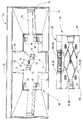
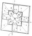
도 6은 본 발명에 따른 소켓(20)의 전개 사시도를 도시한다. 소켓(20)은 예시적인 실시예에서 2개의 연결가능한 하우징 쉘(91)로 이루어지는 소켓 하우징(90)을 포함한다. 소켓 하우징(90)은 2개의 인접한 소켓 하우징 측부(93)가 서로 인접하는 4개의 직사각형 모서리(92)를 포함한다. 적어도 하나, 양호하게는 여러 개 그리고 예시적인 실시예에서, 모든 소켓 하우징 측부(93)에는 적어도 하나의 공급 접속부(95)를 갖는 접속 영역(94)이 있다.6 shows an exploded perspective view of a
공급 접속 영역(94)은 소켓 하우징(90)에 있는 접속 리세스(96)에 의해서 제시된다. 소켓 하우징(90)의 평면도에서, 접속 리세스는 삼각형 형상을 가지며 각 소켓 하우징 측부(93)에서 노치(notch)를 제공한다. 모서리(92)에 인접하는 측부 섹션에서 개시하는, 접속 리세스(96)는 아래 방향으로 2개의 대향 클램핑 측부(97)를 통해서 안으로 테이퍼진다. 클램핑 측부는 중심 측부 섹션(98)을 경유하여 서로 접속된다. 이 중심 측부 섹션(98)에서, 접속 개방부(99)가 각 공급 접속부(95)에 대해서 제공된다. 예시적인 실시예에서, 접속 개방부(99)의 각 절반이 2개의 하우징 쉘(91) 중 하나에 제공된다. 예시적인 실시예에서, 하나 이상의 돌출 클램핑 스트립(100)이 클램핑 측부(97)에 제공된다.The supply connection area 94 is indicated by the connection recess 96 in the
소켓(20)은 상이한 극성을 나타내는 여러 개의 공급 접속부(95)를 포함한다. 공급 접속부들(95) 중 한 부분은 공급 DC 전압의 음극에 할당되고, 다른 부분은 양극에 할당된다. 각 소켓 하우징 측부(93)에는 양극과 연계된 적어도 하나의 공급 접속부(95) 뿐 아니라 음극과 연계된 공급 접속부(95)가 있다. 본원에 기술된 소켓(20)의 예시적인 실시예에 있어서, 양극과 연계된 적어도 하나의 공급 접속부(95) 및 음극과 연계된 공급 접속부(95)는 공급 접속 영역(94)에 배열된다. 발광체(23)와의 접속이 이루어진 상태에서, 공급 접속 영역(94)은 공급 채널(76)이 리세스(75)에서 종결되는 리세스(75) 내의 지점에 위치한다. 이렇게 할 때, 접속 리세스(96)의 최대 폭은 공급 채널(76)의 폭에 대략 대응한다.
각 공급 접속 영역(94)은 예로서 중심 스크류(104)의 도움으로, 소켓 하우징(90)에 분리가능하게 고정될 수 있는 스트레인 경감 수단(strain relief means;103)과 연계된다. 암나사(105)는 소켓 하우징(90) 상에 제공되고 중심 측부 섹션(98)을 향하여 개방된다. 스트레인 경감 수단(103)은 접속 리세스(96)에 적응된 윤곽을 가지는 클램핑 부재(106)이다. 평면도에서, 이는 또한 사다리꼴 윤곽을 가진다. 중심 측부 섹션(98)과 연계된 내측에서, 상기 클램핑 부재는 또한 소켓 하우징(90) 상에 있는 연계된 삽입 슬릿(108) 안으로 삽입될 수 있는 2개의 평탄한 삽입 탭(107)을 가진다. 삽입 슬릿들(108)은 각각 암나사(105) 및 접속 개방부(99) 사이에 위치한다.Each supply connection area 94 is associated with strain relief means 103 that can be releasably secured to the
클램핑 측부(97)와 연계된 측부에는, 클램핑 부재(106)가 클램핑 에지(109)를 가지며, 상기 클램핑 에지는 클램핑 부재(106)가 소켓 하우징(90)에 고정된 상태에서, 연계된 클램핑 측부(97)의 2개의 클램핑 스트립(100)에 대향하는 거리에 위치한다. 클램핑 에지(109)와 클램핑 스트립(100) 사이에 제공된 케이블(78)은 넌-포지티브 방식으로 제자리에 클램핑되고 따라서 스트레인 경감된다. 스크류형 접속부(104,105)의 결과로서, 스트레인 경감은 케이블(78) 상에 있는 당김력을 충분히 흡수할 수 있다. 케이블 클램핑을 위한 클램핑 에지(109) 및 클램핑 스트립(100)의 수는 변화될 수 있다.The clamping
2개의 하우징 쉘(91) 사이의 기계적인 접속은 멈춤쇠 접속에 의해서 이루어질 수 있고, 이러한 경우에 멈춤쇠 후크(110)가 하나의 하우징 쉘(91)에 제공되고, 상기 멈춤쇠 후크는 2개의 하우징 쉘(91)이 함께 스냅될 때, 다른 하우징 쉘(91)에 있는 구체적으로 도시되지 않은 멈춤쇠 카운터 수단(detent counter means)과 멈춤쇠 접속된다.The mechanical connection between the two
공급 접속부(95)는 전기 클램핑 접속부로서 구성된다. 각 공급 접속부(95)는 전기 전도성 접속면(114)을 포함한다. 각 접속면(114)은 그 자유 단부가 안착 위치에서 접속면(114)에 접하거나 또는 적어도 상기 접속면에 대향하는 최소 거리에 위치하는 탄력적인 접속 클램프(115)와 연계된다. 접속면(114)은 적어도 삽입 개방부(99)에 이웃하는 삽입 방향(E)에 평행하게 배열된다. 삽입 개방부(99)의 대향 측부에는, 접속 클램프(115)가 탄력적으로 피봇가능한 방식으로 접속된다. 홈 위치(home position)에서, 접속 클램프(115)는 따라서 접속면(114)에 대해서 경사지는 방식으로 연계된 접속 개방부(99) 뒤로 연장된다. 케이블(78)의 와이어 단부가 삽입될 때, 접속 클램프(115)는 삽입 방향(E)으로 삽입된 와이어 단부에 의해서 관련 접속면(114)으로부터 멀리 피봇되고 절연되지 않은 와이어 단부를 접속면(114)에 대해서 탄력적으로 누르므로, 케이블(78)의 와이어 및 접속면(114) 사이에 안전한 전기 접속이 이루어진다. 이 방식에서, 램프(15)가 장착될 때, 소켓(20)의 매우 단순한 케이블 결합이 달성될 수 있다. 소켓(20)이 여러 개 그리고 예로서 모든 소켓 하우징 측부(93)에서 공급 접속부들(95)을 포함한다면, 공급 라인(16)은 모든 측부로부터 소켓(20)으로 접속될 수 있다.The
소켓 하우징(90)에서, 동일 극성을 나타내는 모든 공급 접속부(95)는 서로에대해서 단락되고 따라서 동일 전위가 된다. 이 결과로서, 여러 개의 소켓(20) 또는 관련 발광체(23)의 매우 단순한 직렬 또는 병렬 접속이 가능해지는데, 그 이유는 공급 접속부(95) 중 하나에 있는 소켓 하우징(90)이 다른 소켓 하우징(90)의 공급 접속부(95)에 선택적으로 전기 접속될 수 있기 때문이다. 도 1에 도시된 램프(15)의 예시적인 실시예에서, 소켓(20)은 서로 직렬로 접속된다[실선 및 띄선으로 공급 라인(16)]. 공급 라인(16)은 모든 소켓(20)을 통해서 직렬로 전압 소스(17)의 양극으로부터 통로가 형성되고(route) 최종 소켓(20)에서 시작하여 양호하게는 전압 소스(17)의 음극으로 뒤로 직접 통로가 형성된다. 이는 도 1에서 점선 공급 라인(16)에서 대안으로 표시된 바와 같이 소켓(20)의 병렬 접속과 동일하게 단순한 방식으로 달성될 수 있다. 소켓(20)은 모든 측부들로부터 공급 접속부(95)를 갖는다는 사실로 인해서, 램프(15)와 여러 소켓(20)과의 배선연결을 위해 필요한 노력이 극히 작아진다.In the
소켓(20)은 또한 각각 할당된 전압 소스(17) 또는 전력 소스(17')에 그룹으로 접속될 수 있고 양호하게는 직렬로 또는 또한 병렬로 접속될 수 있다.The
동일 극성을 나타내는 공급 접속부(95)의 접속면(114)이 공통 단락 커넥터(116)에 제공된다는 점에서, 동일 극성을 나타내는 공급 접속부(95)의 단락이 달성된다. 단락 커넥터(116)는 전기 전도성 구성요소로서 구성된다. 예시적인 실시예에서, 이는 연결 또는 접합 지점들 없이 단일 부재로 균일 재료로서 제조되고 특히 펀칭 굽힘 부분으로서 구성된다. 예로서, 단락 커넥터(116)는 전기 전도성 시트 금속으로부터 펀칭될 수 있고 원하는 형태로 굽혀지며, 따라서 비용 효과적이고 단순한 방식으로 제조될 수 있다. 모든 단락 커넥터(116)는 동일하다. 따라서,소켓(20)에 대해서 단지 하나의 유형 및 단일 형태의 단락 커넥터(116)가 제조될 필요가 있다.A short circuit of the
추가로, 단락 커넥터(116)는 관련 발광체(23)와 전기 접속되기 위해 배치되는 하나 이상의 소켓 접속부(117)를 포함한다. 예시적인 실시예에서, 2개의 소켓 접속부(117)는 각 단락 커넥터(116)에 제공되고, 상기 소켓 접속부는 따라서 단락 커넥터(116)를 통해서 전기적으로 단락된다. 이 결과로서, 동일 극성을 나타내는 공급 접속부(95) 뿐 아니라 동일 극성을 나타내는 소켓 접속부(118)는 예에 따라서 공통 단락 커넥터(116)를 통해서 전기적으로 단락된다. 예시적인 실시예에서, 소켓(20)은 하나의 발광체를 각각 아노드 및 캐소드를 구비하는 2개의 반도체 발광 요소들과 접속하기 위해서 배치된다. 결과적으로, 양극성을 나타내는 2개의 소켓 접속부(117) 및 음극성을 나타내는 2개의 소켓 접속부(117)가 제공된다. 상이한 극성을 갖는 소켓 접속부(117)의 쌍들의 수는 따라서 발광체(23)에서 반도체 발광 요소들의 수에 따라 좌우될 수 있다.Additionally, the shorting
각 단락 커넥터(116)는 필수적으로 하나의 평면에서 연장되는 베이스 섹션(118)을 포함한다. 이 베이스 섹션(118)은 여러 개의 개방부들(119)을 구비할 수 있다. 소켓 하우징(90)에 제공되는 상이한 배치 및 접속 수단은 예로서 도 7에 도시된 바와 같이, 개방부(19)를 통해서 연장될 수 있다.Each shorting
소켓 접속부(117)는 베이스 섹션(118)의 2개의 대향 단부들 각각에 제공된다. 소켓 접속부(117)는 베이스 섹션(118)으로부터 멀리 가로방향으로 연장되는 대향으로 배열된 2개의 접속 탭(120)을 포함한다. 베이스 섹션(118)에서 개시되는, 2개의 접속 탭(120)은 초기에는 서로로부터 멀리 킹크 지점(kink point;121)까지 연장되고, 킹크 지점에서 개시되어서 다시 서로를 향하여 그들의 각 자유 단부까지 연장되고, 자유 단부들은 서로로부터 거리를 두고 있다. 2개의 접속 탭(121)은 동일하게 구성된다. 소켓 접속부는 중심 평면에 대해서 대칭이다. 단락 커넥터(116)의 소켓 접속부(117)를 통과하는 각 중심 평면은 평행 방향으로 거리를 두고 연장한다. 소켓 접속부(117)의 중심 평면은 베이스 섹션(118)을 통해서 길이방향 중심축에 대해서 대략 45도 각도가 형성된다.A
단락 커넥터(116)에 제공된 접속면(114)은 필수적으로 평면형 접속 부분(122)에 제공된다. 접속면(114)은 베이스 섹션(118)을 통해서 길이방향 축에 대하여 대략 45도의 각도로 기울어진다. 상기 접속면들은 소켓 접속부(117)의 중심 평면에 평행하거나 또는 그에 직각으로 연장된다. 접속면(114)을 갖는 접속 부분(122)은 필수적으로 베이스 섹션(118)으로부터 직각으로 연장된다. 접속 탭(120)의 자유 단부 및 접속 부분(122)의 자유 단부 에지는 베이스 섹션(118)으로부터 거리를 두고 동일 측부에 배열되고 바람직하게는 약 하나의 평면에서 위치할 수 있다. 소켓 접속부(117)로부터 분리되는, 단락 커넥터(116)는 길이방향 중심 평면에 대칭이 되도록 설계된다.The
단락 커넥터(116)의 각 접속면(114)은 다른 공급 접속 영역(94)에 할당된다. 단락 커넥터(116) 중 하나는 양극성을 나타내는 공급 접속부(95)의 접속면(114)을 가지며, 다른 단락 커넥터(116)는 음극성을 나타내는 공급 접속부(95)의 접속면(114)을 가진다.Each
동일 극성을 나타내는 직접 인접한 공급 접속 영역(94)의 공급 접속부(95)는 원주방향에서 볼 때 소켓 하우징(90) 주위로 서로 이웃하게 배열된다. 즉, 모서리(92)에서 시작하고 동일 극성을 나타내는 공급 접속부(95)는 양 소켓 하우징 측부(93)를 따른다. 이들 2개의 공급 접속부(95)는 상이한 공급 접속부(95)에 대해서 접속 클램프(115)를 형성하는 단부 섹션을 갖는 공통 클램핑 부재(125)에 할당된다. 2개의 접속 클램프(115)는 중심 부재(126)를 통해서 서로 접속된다. 접속 클램프(115)는 중심 부재(126)로부터 멀리 가로 방향으로 연장되고, 이 경우에 그 거리가 증가한다. 중심 부재(126) 및 접속 클램프(115)는 100 내지 110 도의 범위에 있는 각도에서 마주 본다. 예시적인 실시예에서, 접속 클램프(115) 및 중심 부재(126) 사이의 변이는 2개의 각도가 형성되도록 구성된다. 접대 부분(127)은 중심 부재(126)의 하나의 길이방향 에지에서 직각으로 구부려지고, 상기 접대 부분은 일반적인 사용 위치에서 2개의 하우징 절반부(91) 중 하나의 베이스 면에 의해서 지지된다. 중심 부재(126) 및 클램핑 요소(115) 사이의 변이 영역에서, 접속 클램핑 부재(125)는 소켓 하우징(90)의 각각의 하나의 지지 돌출부(128)에 대해서 접한다. 지지 돌출부(128)는 2개의 하우징 절반부(91) 중 하나에서 접속 개방부(99)에 이웃하는 접속면(114)에 대향하게 배열된다. 접대 부분(127)은 2개의 지지 돌출부(128) 사이에 배열된다.The
예에 따라서, 4개의 접속 클램프 부재(125) 중 2개 그리고 전체는 양극성을 나타내는 4개의 공급 접속부(95) 및 음극성을 나타내는 4개의 공급 접속부에 대해서 제공된다.According to the example, two and all four of the four
일반적인 사용 위치에서, 2개의 단락 커넥터(116)는 소켓 하우징(90)에서 교차하고, 이들은 교차 지점에서 절연 거리(A)에서 서로에 대해서 연장된다. 교차 지점에서, 2개의 단락 커넥터(116) 사이에 절연 재료가 제공되지 않는다. 교차 지점에서 2개의 단락 커넥터(116) 사이의 영역은 자유 공간으로서 구성된다. 교차 지점에서 절연 거리(A)를 달성하기 위하여, 2개의 단락 부재(116) 중 하나는 후방 위치에 배열되고, 예로서 소켓 하우징(90)에서 각각의 다른 단락 부재(116)에 대해서 90 만큼 회전한다. 접속 부분(122)의 자유 단부 및/또는 하나의 단락 부재(116) 중 접속 탭(120)은 양호하게는 각각의 다른 단락 부재(116)의 베이스 섹션(118)이 위치하는 평면에서 위치한다. 접속 부분(122)의 자유 단부 및/또는 하나의 단락 부재(116)의 접속 탭(120)이 위치하는- 다른 단락 부재(116)의 베이스 섹션(118)으로부터의- 적어도 평면의 거리는 2개의 단락 부재들(116) 사이의 거리 보다 작다. 하나의 단락 커넥터들의 베이스 섹션(118)은 하나의 하우징 절반부(91)의 내측에 대해서 접하고, 각각의 다른 단락 커넥터(116)의 베이스 섹션(118)은 각각의 다른 하우징 쉘(91)의 내측에 대해서 접한다. 다시 말해서, 2개의 단락 커넥터(116)의 베이스 섹션(118)은 소켓 하우징(90)에 있는 필수적으로 평행한 평면들에서 절연 거리(A)에서 배열된다.In a general use position, the two shorting
소켓(20)은 관련 발광체(23)와의 소켓의 기계적 및 전기적 접속을 위해서 배치된 소켓 접속 디바이스(130)를 포함한다. 소켓 접속 디바이스(130)는 예에 따라서 단락 커넥터(116)에 제공되는 소켓 접속부(117)를 포함한다. 또한, 소켓 접속 디바이스(130)는 단독으로 또는 소켓 접속부(117)와 함께 발광체(23)와의 기계적인 접속을 보장하는 기계적 접속 수단을 포함한다. 소켓 접속 디바이스(130)는 소켓 하우징(90)의 접속 측부(131)에 제공되고 이 접속 측부(131)로부터 접근될 수 있다. 접속 측부(131)에 대향하는 장착 측부(132)는 소켓 하우징을 장착면, 예로서 실내의 벽 또는 천장 또는 임의의 다른 표면에 장착하기 위하여 배치된다.The
본원에 기술된 예시적인 실시예에서, 소켓 접속 디바이스(130)의 기계적인 접속 수단은 소켓 하우징 개방부(134)에 인접하는 소켓 하우징(90)에 배열되는 멈춤쇠 에지(133)에 의해서 형성된다. 탄력적으로 지지되는 유지 요소(135)는 소켓 하우징 개방부(134)의 2개의 대향 측부들에 몰딩되고, 상기 유지 요소는 소켓 하우징 개방부(134)에 인접하는 탄성적으로 피봇가능한 방식으로 힌지결합된다. 그들의 각 자유 단부에서, 유지 요소는 각각의 대향 유지 요소(135)를 향하여 돌출하는 멈춤쇠 에지(133)를 지지한다. 멈춤쇠 벌지(73)를 구비하는 멈춤쇠 돌출부(72)는 소켓(20) 및 발광체(23) 사이의 기계적 연결을 형성하기 위하여 소켓 하우징 개방부(134)를 통해서 소켓 하우징(90) 안으로 연장될 수 있고 멈춤쇠 에지(133) 주위로 연장된다.The mechanical connection means of the
또한, 소켓 접속부(117)가 경유하여 접근할 수 있는 소켓 접속 개방부(135)는 소켓 하우징(90)의 접속 측부(131)에 제공된다. 예시적인 실시예에서, 각각의 소켓 접속부(117)에는 2개의 소켓 접속 개방부(135)가 할당되므로, 소켓 접속부(117)의 양 접속 탭(120)은 각각의 하나의 소켓 하우징 개방부(135)를 경유하여 접근할 수 있다. 소켓 접속 개방부(135)는 우연한 접촉에 대한 보호 이유로 인하여 슬릿 형태를 가지므로, 소켓 접속부(117)를 손가락으로 접촉하는 것은 불가능하게 된다.A
발광체 접속부(46)가 소켓 접속부(117)에 접하게 된다는 점에서, 발광체(23) 및 소켓(20) 사이의 전기 접촉이 보장된다. 본원에 기술된 실시예에서, 발광체 접속부(46)는 소켓 접속부(117) 주위로 연장된다. 이렇게 할 때, 소켓 접속부(117)의 2개의 접속 탭(120)은 관련 발광체 접속부(46)의 2개의 접촉 날개부(48) 사이에 위치한다. 이렇게 할 때, 각각의 하나의 접촉 날개부(48)는 하나의 접속 탭(120)과 접한다. 접촉 날개부(48) 뿐 아니라 접촉 탭(120)의 스프링 탄성 지지로 인하여, 발광체(23) 및 소켓(20) 사이의 전기 접촉이 이루어질 때 기계적인 클램핑 힘이 또한 발생한다. 이러한 기계적인 클램핑 힘이 충분하다면, 발광체(23) 및 소켓(20) 사이의 추가적인 기계 접속 수단이 생략될 수 있다.Electrical contact between the light emitting
소켓 접속 디바이스(130)는 접속 측부(131) 상의 중심(P)에 대해 점대칭이 되도록 제공된다. 양자의 소켓 하우징 개방부(134)는 소켓 하우징(90)의 접속 측부(131)에서 중심(P)으로부터 동일 거리에서 중심(P)을 통한 반경방향 직선에 제공된다. 이렇게 할 때, 소켓 하우징(90)은 중심(P)을 통한 회전축 주위에서 180도 만큼 회전할 수 있고 상기 2개의 회전 위치에서 발광체(23)와 접속될 수 있다.The
본 발명은 램프(15)를 위한 발광체(23) 및 소켓(20)에 관한 것이다. 소켓(20)의 형태부들은 또한 발광체(23)의 형태부들과 독립적으로 이행될 수 있다. 발광체(23)는 양호하게는 평면형 발광면(24)을 가진다. 하나 이상의 반도체 발광 요소는 발광체 하우징(30)에 배열된다. 소켓(20)과의 기계적 및 전기적 접속을 위해 필요한 발광체 접속 디바이스(70)는 발광면(24)에 대향하는 발광체(23)의 후방면(66)에 제공된다. 발광체(23)의 치수는 양호하게는 소켓(20)의 치수 보다 크므로, 발광면(24)의 방향으로 볼 때 발광체(23)는 소켓(20)을 완전히 커버한다. 이 결과로서, 특히 시각적으로 만족을 주는 외형을 달성할 수 있다. 여러 개의 소켓 하우징 측부(93)에서, 소켓은 공급 접속 영역을 포함하므로, 소켓(20)의 전기 공급 및 배선은 상이한 측부로부터 또는 또한 동시에 여러 측부들로부터 선택적으로 달성될 수 있다. 공급 접속 영역(94)의 수 및 배열과는 무관한, 동일 극성을 나타내는 여러 개의 전기 공급 접속부(95)는 소켓(20)에 제공된다. 동일 극성을 나타내는 이들 공급 접속부(95)는 전기적으로 단락된다. 각각의 하나의 단락 커넥터(116)는 동일 극성을 나타내는 공급 접속부를 단락시키기 위하여 배치되고, 이 경우에 특히 2개의 동일한 단락 커넥터(116)가 소켓 하우징(90)에 배열된다. 전압이 대략 200 V에 도달할 수 있는 DC 전압이 소켓(20)에 인가된다. 이러한 소켓(20) 및 발광체(23)로써, 시각적으로 만족을 주는 전체 외형을 특징으로 하는 램프(15)의 큰 전체 발광면을 매우 단순한 모듈형 방식으로 달성할 수 있다.
The present invention relates to a light emitter (23) and a socket (20) for a lamp (15). The features of the
도면부호 목록
15. 램프
16. 공급 라인
17. 전압 소스
18. 스위치
20. 소켓
21. 횡열
22. 종열
23. 발광체
24. 23의 발광면
25. 캐리어 요소
26. 전방 플레이트 또는 포일
27. 후방 플레이트 또는 포일
30. 발광체 하우징
31. 프레임
32. 하우징 후방벽
33. 광 출구 개방부
34. 스트립
35. 접대면
36. 스트립 섹션
39. 발광체 접촉 부분
40. 발광체 접촉부
41. 접촉 지점
42. 접촉 탭
42a. 42의 평면형 섹션
42b. 42의 자유 단부
43. 슬릿
44. 39의 제 1 단부
45. 39의 제 2 단부
46. 발광체 접속부
47. 교차부재
48. 접촉 날개부
49. 굽힘 지점
51. 39의 유지 섹션
52. 유지 클램프
53. 오프셋
54. 클램핑 탭
55. 보유 개방부
56. 보유 돌출부
57. 스프링 탄성 구역
58. 탭 유지 부분
59. 스프링 탭
60. 베어링 요소
63. 수용 영역
64. 32의 내측
65. 발광체 접속 개방부
66. 후방면
67. 로킹 고리
68. 프레임 측부
70. 발광체 접속 디바이스
71. 멈춤쇠 수단
72. 멈춤쇠 돌출부
73. 멈춤쇠 벌지
74a. 73의 경사진 표면
74b. 73의 멈춤쇠 접대면
75. 리세스
76. 공급 채널
77. 바닥
78. 16의 케이블
79. 강직성 리브
80. 키잉 요소
90. 소켓 하우징
91. 하우징 쉘
92. 90의 모서리
93. 소켓 하우징 측부
94. 공급 접속 영역
95. 공급 접속부
96. 접속 리세스
97. 클램핑 측부
98. 중심 측부 섹션
99. 접속 개방부
100. 클램핑 스트립
103. 스트레인 경감 수단
104. 스크류
105. 암나사
106. 클램핑 부재
107. 삽입 탭
108. 삽입 슬릿
109. 클램핑 에지'
110. 멈춤쇠 후크
114. 접속면
115. 접속 클램프
116. 단락 커넥터
117. 소켓 접속부
119. 개방부
120. 접속 탭
121. 킹크 지점
122. 접속 부분
125. 접속 클램프 부재
126. 중심 부재
127. 접대 부분
128. 지지 돌출부
130. 소켓 접속 디바이스
131. 접속 측부
132. 장착 측부
133. 멈춤쇠 에지
134. 소켓 하우징 개방부
135. 소켓 접속 개방부
E삽입 방향
M23의 중심
P20의 중심List of reference marks
15. Lamp
16. Supply Line
17. Voltage Source
18. Switch
20. Socket
21. Transverse heat
22. Heath
23. Light emitter
24. The light emitting surface of 23
25. Carrier element
26. Front plate or foil
27. A rear plate or foil
30. Illuminator housing
31. Frame
32. Barrier after housing
33. Light outlet opening
34. Strip
35. Reception surface
36. Strip section
39. Light emitting body contact portion
40. Light-
41. Contact point
42. Contact tab
42a. 42 planar sections
42b. 42 free end
43. Slit
44. First end of 39
45. Second end of 39
46. Light-
47. Cross member
48. Contact wing
49. Bending point
51.
52. Retaining clamp
53. Offset
54. Clamping tab
55. Holding open section
56. Retention projection
57. Spring elastic zone
58. Tab hold portion
59. Spring tab
60. Bearing element
63. Accommodation area
64. Inside of 32
65. An illuminator connection opening
66. Rear view
67. Locking ring
68. The frame side
70. An illuminator connecting device
71. Detent means
72. Detent protrusion
73. A detent bulge
74a. 73 sloping surface
74b. 73 detent reception surface
75. The recess
76. Supply channel
77. bottom
78. 16 cables
79. Rigid ribs
80. Keying factor
90. Socket housing
91. Housing shell
92. The corner of 90
93. Socket housing side
94. Supply connection area
95. Supply connection
96. Connection recess
97. Clamping side
98. Center side section
99. Connection opening
100. Clamping strip
103. Strain relief means
104. Screw
105. Female threads
106. The clamping member
107. Insert tab
108. Insert slit
109. Clamping edge '
110. Detent hook
114. Connecting face
115. Connection Clamp
116. Short-circuit connector
117. Socket connection
119. Opening
120. Connection tab
121. Kink Point
122. Connecting portion
125. The connection clamp member
126. The center member
127. Hospitality section
128. Support protrusions
130. A socket connection device
131. Connecting side
132. Mounting side
133. Detent edge
134. Socket housing opening
135. A socket connection opening
E insertion direction
Center of
Center of
Claims (20)
Translated fromKorean상기 발광체(23)와 연계된 접속 측부(131) 상에서, 상기 발광체(23)와 기계적 및 전기적 접속을 이루기 위해 배치되는 소켓 접속 디바이스(130)를 포함하는 소켓 하우징(90);
상기 소켓(20)을 장착면에 장착하기 위한, 상기 접속 측부(131)의 반대편에 있는 상기 소켓 하우징(90)의 장착 측부(132); 및
상기 소켓 하우징(90)의 상기 장착 측부(132) 및 상기 접속 측부(131) 사이에 배치되는 소켓 하우징 측부들(93)로서, 상기 소켓(20)과 공급 라인(16)과의 전기 접속을 위한 공급 접속부들(95)이 상기 소켓 하우징 측부들(93)의 적어도 하나에 제공되는, 상기 소켓 하우징 측부(93);를 포함하고,
단락 커넥터들(116)이 상기 소켓 하우징(90)에 배열되고, 상기 단락 커넥터들은 복수의 접속면들(114)을 가지며, 단락될 각각의 공급 접속부(95)는 동일한 단락 커넥터(116)의 접속면들(114) 중 하나에 할당되고,
상기 공급 접속부들(95)은 양극성(+) 또는 음극성(-)을 나타내고, 동일 극성(+ 또는 -)을 나타내는 모든 공급 접속부들(95)은 서로에 대해 전기 단락되는, 발광체용 소켓.As the socket for the light emitter 23,
A socket housing (90) including a socket connecting device (130) arranged on the connecting side portion (131) associated with the light emitting body (23) for making mechanical and electrical connection with the light emitting body (23);
A mounting side 132 of the socket housing 90 opposite the connection side 131 for mounting the socket 20 to the mounting surface; And
Socket housing sides 93 disposed between the mounting side 132 and the connecting side 131 of the socket housing 90 for electrical connection between the socket 20 and the supply line 16, The socket housing side portion (93), wherein supply contacts (95) are provided on at least one of the socket housing side portions (93)
The shorting connectors 116 are arranged in the socket housing 90 and the shorting connectors have a plurality of connecting surfaces 114 and each supply connecting portion 95 to be short-circuited is connected to the same shorting connector 116 Is assigned to one of the faces 114,
Wherein the supply connections 95 represent positive or negative polarity and all the supply connections 95 representing the same polarity (+ or -) are electrically shorted to each other.
각각의 복수의 공급 접속부들(95)이 복수의 소켓 하우징 측부들(93)에 제공되는 것을 특징으로 하는 발광체용 소켓.The method according to claim 1,
Wherein each of the plurality of supply contacts (95) is provided in a plurality of socket housing sides (93).
하나의 스트레인 경감 수단(103)이 각각의 공급 접속부(95)에 대해서 제공되는 것을 특징으로 하는 발광체용 소켓.3. The method of claim 2,
Characterized in that one strain relief means (103) is provided for each supply connection (95).
상기 스트레인 경감 수단(103)은 상기 소켓 하우징(90)에 분리가능하게 체결되는 것을 특징으로 하는 발광체용 소켓.The method of claim 3,
Wherein the strain relief means (103) is detachably fastened to the socket housing (90).
상기 공급 접속부들(95)을 포함하는 하나의 소켓 하우징 측부(93)에서, 적어도 하나의 공급 접속부(95)는 양극에 할당되고 적어도 하나의 공급 접속부(95)는 음극에 각각 할당되는 것을 특징으로 하는 발광체용 소켓.3. The method according to claim 1 or 2,
Characterized in that, in one socket housing side (93) comprising the supply connections (95), at least one supply connection (95) is assigned to the anode and at least one supply connection (95) Lt; / RTI >
상기 소켓 접속 디바이스(130)는 상기 발광체(23)의 전기 접속을 위해 배치되는 전기 소켓 접속부들(117)을 포함하는 것을 특징으로 하는 발광체용 소켓.The method according to claim 1,
Characterized in that the socket connection device (130) comprises electrical socket connections (117) arranged for electrical connection of the light emitter (23).
동일 극성(+ 또는 -)을 나타내는 복수의 소켓 접속부들(117)이 제공되고 동일 극성(+ 또는 -)을 나타내는 상기 소켓 접속부들(117)은 서로에 대해서 전기 단락되는 것을 특징으로 하는 발광체용 소켓.9. The method of claim 8,
Characterized in that a plurality of socket connection portions (117) indicating the same polarity (+ or -) are provided and the socket connection portions (117) indicating the same polarity (+ or -) are shorted to each other .
동일 극성(+ 또는 -)을 나타내는 상기 소켓 접속부들(117) 사이의 전기 단락은 단일 단락 커넥터(116)에 의해서 각각 이루어지는 것을 특징으로 하는 발광체용 소켓.10. The method of claim 9,
Characterized in that the electrical short between the socket connections (117) indicating the same polarity (+ or -) is made by a single short-circuit connector (116), respectively.
단락 커넥터(116)가 음극(-)에 할당되고 단락 커넥터(116)가 양극(+)에 할당되며, 상기 단락 커넥터들은 동일 형태를 갖는 것을 특징으로 하는 발광체용 소켓.11. The method of claim 10,
Characterized in that the shorting connector (116) is assigned to the negative (-) and the shorting connector (116) is assigned to the positive (+) and the shorting connectors have the same shape.
각각의 단락 커넥터(116)는 베이스 섹션(118) 및 상기 베이스 섹션(118)으로부터 각도를 이루며 연장되는 접속 부분들(122)을 가지며, 상기 접속 부분들의 각각은 접속면(114)을 구비하는 것을 특징으로 하는 발광체용 소켓.11. The method of claim 10,
Each shorting connector 116 has a base section 118 and connecting sections 122 extending at an angle from the base section 118 and each of the connecting sections having a connecting surface 114 Characterized in that it comprises a socket for a luminous body.
2개의 상이한 극들(+ 또는 -)에 할당된 상기 단락 커넥터들(116)은 상기 소켓 하우징(90)에서 절연 거리(A)를 두고 배열되는 것을 특징으로 하는 발광체용 소켓.11. The method of claim 10,
Characterized in that the shorting connectors (116) assigned to two different poles (+ or -) are arranged at an insulation distance (A) in the socket housing (90).
상기 2개의 단락 커넥터들(116)의 베이스 섹션들(118)은 상기 절연 거리(A)를 유지하면서 교차 지점에서 교차되는 것을 특징으로 하는 발광체용 소켓.14. The method of claim 13,
Wherein the base sections (118) of the two shorting connectors (116) intersect at an intersection while maintaining the insulation distance (A).
플레이트형 또는 포일형 캐리어 요소(25)를 포함하는 발광체(23)로서, 상기 캐리어 요소는 반도체 발광 요소의 구성요소이거나 또는 반도체 발광 요소를 포함하는 상기 발광체(23);
상기 발광체(23)의 발광체 하우징(30)으로서, 상기 발광체 하우징은 상기 캐리어 요소(25)를 지지하고, 전방 측부 상에서 광 출구 개방부(33)를 구비하고, 상기 전방 측부의 반대편에 있는 후방면(66) 상에서 발광체 접속 디바이스(70)를 구비하는, 상기 발광체 하우징(30); 및
상기 발광체 하우징(30)과 연계된 접속 측부(131) 상에서 소켓 접속 디바이스(130)를 구비하는 소켓(20)으로서, 상기 발광체 접속 디바이스(70)는 상기 소켓 접속 디바이스(130)와 함께 상기 발광체(23) 및 상기 소켓(20) 사이에 기계적 및 전기적 접속을 이루도록 배치되는, 상기 소켓(20);을 포함하고,
상기 소켓(20)은 소켓 하우징(90) 및 상기 소켓 하우징(90)에 배열되는 단락 커넥터들(116)을 추가로 포함하고, 상기 단락 커넥터들은 복수의 접속면들(114)을 가지며, 단락될 각각의 공급 접속부(95)는 동일한 단락 커넥터(116)의 접속면들(114) 중 하나에 할당되고,
상기 공급 접속부들(95)은 양극성(+) 또는 음극성(-)을 나타내고, 동일 극성(+ 또는 -)을 나타내는 모든 공급 접속부들(95)은 서로에 대해 전기 단락되는, 램프.As a lamp,
A light emitting body (23) comprising a plate or foil-shaped carrier element (25), said carrier element being a component of a semiconductor light emitting element or comprising a semiconductor light emitting element;
A light emitter housing (30) of the light emitter (23), the light emitter housing supporting the carrier element (25) and having a light exit opening (33) on the front side, (70) on the light emitter housing (66); And
A socket (20) comprising a socket connection device (130) on a connection side portion (131) associated with the luminous body housing (30), said luminous means connection device (70) 23) and the socket (20), the socket (20) being arranged to make a mechanical and electrical connection between the socket
The socket 20 further includes shorting connectors 116 arranged in the socket housing 90 and the socket housing 90 and having a plurality of connecting surfaces 114, Each supply contact 95 is assigned to one of the contact faces 114 of the same short-circuit connector 116,
The supply connections 95 represent positive or negative polarity and all the supply connections 95 representing the same polarity (+ or -) are electrically shorted to each other.
상기 광 출구 개방부(33)는 상기 발광체(23)의 평면형 발광면(24)을 한정하는 것을 특징으로 하는 램프.17. The method of claim 16,
Characterized in that the light exit opening (33) defines a planar light emitting surface (24) of the light emitter (23).
상기 발광면(24)의 방향으로 직각으로 바라본 상기 발광체(23)는 상기 소켓(20)을 완전히 커버하는 것을 특징으로 하는 램프.18. The method of claim 17,
Wherein the light emitter (23) viewed at a right angle to the direction of the light emitting surface (24) completely covers the socket (20).
복수의 소켓들(20)이 제공되는 것을 특징으로 하는 램프.17. The method of claim 16,
Characterized in that a plurality of sockets (20) are provided.
상기 소켓들(20) 상에 배열된 상기 발광체들(23)의 발광면들(24)은 공통 평면 상에 위치되는 것을 특징으로 하는 램프.20. The method of claim 19,
Wherein the light emitting surfaces (24) of the light emitters (23) arranged on the sockets (20) are located on a common plane.
Applications Claiming Priority (3)
| Application Number | Priority Date | Filing Date | Title |
|---|---|---|---|
| DE102010038252ADE102010038252A1 (en) | 2010-10-18 | 2010-10-18 | Socket for a luminaire with OLED bulb |
| DE102010038252.3 | 2010-10-18 | ||
| PCT/EP2011/068194WO2012052441A2 (en) | 2010-10-18 | 2011-10-18 | Socket for a lamp having an oled illuminant |
Publications (2)
| Publication Number | Publication Date |
|---|---|
| KR20140038343A KR20140038343A (en) | 2014-03-28 |
| KR101916653B1true KR101916653B1 (en) | 2018-11-08 |
Family
ID=44907823
Family Applications (1)
| Application Number | Title | Priority Date | Filing Date |
|---|---|---|---|
| KR1020137012668AExpired - Fee RelatedKR101916653B1 (en) | 2010-10-18 | 2011-10-18 | Socket for a lamp having an oled illuminant |
Country Status (7)
| Country | Link |
|---|---|
| US (1) | US9423108B2 (en) |
| EP (1) | EP2630403B1 (en) |
| JP (1) | JP5768291B2 (en) |
| KR (1) | KR101916653B1 (en) |
| CN (1) | CN103403440B (en) |
| DE (1) | DE102010038252A1 (en) |
| WO (1) | WO2012052441A2 (en) |
Families Citing this family (8)
| Publication number | Priority date | Publication date | Assignee | Title |
|---|---|---|---|---|
| JP5789757B2 (en)* | 2011-03-04 | 2015-10-07 | パナソニックIpマネジメント株式会社 | Lighting device |
| DE102011082209A1 (en) | 2011-09-06 | 2013-03-07 | Osram Opto Semiconductors Gmbh | LIGHT AND USE |
| JP2013182732A (en)* | 2012-02-29 | 2013-09-12 | Toshiba Lighting & Technology Corp | Lighting fixture |
| DE102012223162B4 (en)* | 2012-12-14 | 2022-08-25 | Pictiva Displays International Limited | AREA LIGHT SYSTEM |
| DE102013212671B4 (en) | 2013-06-28 | 2018-07-19 | Itz Innovations- Und Technologiezentrum Gmbh | Variable ceiling or wall light system as well as base plate and light module for this |
| DE202014100951U1 (en)* | 2014-03-03 | 2015-06-09 | Zumtobel Lighting Gmbh | Luminaire with support element and releasably attachable light module |
| DE202015105853U1 (en)* | 2015-11-04 | 2017-02-08 | Zumtobel Lighting Gmbh | lighting device |
| CN107489991B (en)* | 2017-08-08 | 2023-08-04 | 厦门阳光恩耐照明有限公司 | External wiring structure of lamp and lamp |
Citations (2)
| Publication number | Priority date | Publication date | Assignee | Title |
|---|---|---|---|---|
| US20050148241A1 (en)* | 2001-05-31 | 2005-07-07 | Ran Kohen | Quick connect device for electrical fixtures |
| JP2010135250A (en)* | 2008-12-08 | 2010-06-17 | Sumitomo Wiring Syst Ltd | Connector |
Family Cites Families (33)
| Publication number | Priority date | Publication date | Assignee | Title |
|---|---|---|---|---|
| GB224553A (en)* | 1923-11-07 | 1926-04-07 | Max Sieverts Fabriks Aktiebola | Waterproof electric fittings |
| JPS5649047Y2 (en) | 1979-03-29 | 1981-11-16 | ||
| FR2623028B1 (en)* | 1987-11-10 | 1992-12-04 | Claude Sa | LUMINAIRE CONNECTION BOX |
| US6184628B1 (en)* | 1999-11-30 | 2001-02-06 | Douglas Ruthenberg | Multicolor led lamp bulb for underwater pool lights |
| US6558021B2 (en)* | 2001-08-10 | 2003-05-06 | Leotek Electronics Corporation | Light emitting diode modules for illuminated signs |
| JP3928383B2 (en) | 2001-08-17 | 2007-06-13 | 松下電工株式会社 | LED lighting fixtures |
| JP3928385B2 (en) | 2001-08-24 | 2007-06-13 | 松下電工株式会社 | lighting equipment |
| US6565231B1 (en) | 2002-05-28 | 2003-05-20 | Eastman Kodak Company | OLED area illumination lighting apparatus |
| US6787990B2 (en)* | 2002-05-28 | 2004-09-07 | Eastman Kodak Company | OLED area illumination light source having flexible substrate on a support |
| US6819036B2 (en) | 2002-05-28 | 2004-11-16 | Eastman Kodak Company | OLED lighting apparatus |
| DE10392736T5 (en) | 2002-10-25 | 2005-07-07 | Moriyama Sangyo K.K. | light module |
| US7108392B2 (en)* | 2004-05-04 | 2006-09-19 | Eastman Kodak Company | Tiled flat panel lighting system |
| JP4788601B2 (en)* | 2004-09-24 | 2011-10-05 | 東芝ライテック株式会社 | Annular fluorescent lamp and lighting fixture |
| US20060082315A1 (en) | 2004-10-20 | 2006-04-20 | Timothy Chan | Method and system for attachment of light emmiting diodes to circuitry for use in lighting |
| JP4548219B2 (en) | 2005-05-25 | 2010-09-22 | パナソニック電工株式会社 | Socket for electronic parts |
| JP2007139016A (en) | 2005-11-16 | 2007-06-07 | Saginomiya Seisakusho Inc | Electric control valve and refrigeration cycle equipment |
| JP5033138B2 (en) | 2005-12-16 | 2012-09-26 | コーニンクレッカ フィリップス エレクトロニクス エヌ ヴィ | Lighting system with interconnectable lighting modules |
| JP4618171B2 (en) | 2006-03-15 | 2011-01-26 | パナソニック電工株式会社 | Luminescent panel lighting fixture |
| JP4528277B2 (en) | 2006-03-31 | 2010-08-18 | 三菱電機株式会社 | lighting equipment |
| DE102006015437A1 (en) | 2006-03-31 | 2007-10-04 | Merck Patent Gmbh | Glowing floor tile for e.g. bathroom, has layer structure with vision plate and illuminant, where organic LED-layer is provided as illuminant, where rear side of rest- and/or spring contact of illuminant is provided opposite to vision plate |
| US7549786B2 (en) | 2006-12-01 | 2009-06-23 | Cree, Inc. | LED socket and replaceable LED assemblies |
| DE202006018985U1 (en)* | 2006-12-15 | 2007-03-29 | Patent-Treuhand-Gesellschaft für elektrische Glühlampen mbH | Lamp has lamp base and at least one light-emitting semiconductor element having electrical contacts and connecting parts |
| DE202006019239U1 (en) | 2006-12-19 | 2008-04-30 | Bender & Wirth Gmbh & Co. | Device for light bulbs |
| DE102007023019B4 (en)* | 2007-05-15 | 2010-02-18 | Phoenix Contact Gmbh & Co. Kg | Locking clip for connector housing |
| DE102007041136A1 (en)* | 2007-08-30 | 2009-03-05 | Osram Opto Semiconductors Gmbh | LED housing |
| DE102008024776A1 (en) | 2007-09-28 | 2009-11-26 | Osram Gesellschaft mit beschränkter Haftung | Illuminant, particularly magnetically attached illuminant for lighting system, has individual light sources with electrical connection, which is magnetically adhered, particularly with two magnetically adhered electrical connections |
| WO2009072386A1 (en) | 2007-12-06 | 2009-06-11 | Konica Minolta Holkings, Inc. | Lighting unit panel |
| CN201302052Y (en)* | 2008-10-30 | 2009-09-02 | 刘玉鸣 | Multifunctional rechargeable LED lamp set |
| CN101413633A (en)* | 2008-11-11 | 2009-04-22 | 英飞特电子(杭州)有限公司 | Wall type LED lamp |
| CN101813249A (en)* | 2009-02-23 | 2010-08-25 | 简孝伦 | Led lamp structure |
| KR101496473B1 (en) | 2009-03-05 | 2015-02-27 | 타이코에이엠피(유) | Light emitting device |
| US20110318954A1 (en)* | 2010-06-24 | 2011-12-29 | Lin de-hui | Socket structure of miniature light bulb set |
| DE102010038251A1 (en) | 2010-10-18 | 2012-04-19 | Koninklijke Philips Electronics N.V. | OLED illuminant for a luminaire |
- 2010
- 2010-10-18DEDE102010038252Apatent/DE102010038252A1/ennot_activeWithdrawn
- 2011
- 2011-10-18WOPCT/EP2011/068194patent/WO2012052441A2/enactiveApplication Filing
- 2011-10-18USUS13/880,228patent/US9423108B2/enactiveActive
- 2011-10-18JPJP2013534298Apatent/JP5768291B2/ennot_activeExpired - Fee Related
- 2011-10-18KRKR1020137012668Apatent/KR101916653B1/ennot_activeExpired - Fee Related
- 2011-10-18EPEP11773243.8Apatent/EP2630403B1/ennot_activeNot-in-force
- 2011-10-18CNCN201180060769.7Apatent/CN103403440B/ennot_activeExpired - Fee Related
Patent Citations (2)
| Publication number | Priority date | Publication date | Assignee | Title |
|---|---|---|---|---|
| US20050148241A1 (en)* | 2001-05-31 | 2005-07-07 | Ran Kohen | Quick connect device for electrical fixtures |
| JP2010135250A (en)* | 2008-12-08 | 2010-06-17 | Sumitomo Wiring Syst Ltd | Connector |
Also Published As
| Publication number | Publication date |
|---|---|
| EP2630403A2 (en) | 2013-08-28 |
| US9423108B2 (en) | 2016-08-23 |
| CN103403440B (en) | 2016-02-10 |
| DE102010038252A1 (en) | 2012-04-19 |
| JP2013546125A (en) | 2013-12-26 |
| EP2630403B1 (en) | 2016-12-14 |
| WO2012052441A2 (en) | 2012-04-26 |
| KR20140038343A (en) | 2014-03-28 |
| JP5768291B2 (en) | 2015-08-26 |
| WO2012052441A3 (en) | 2012-07-05 |
| US20140140041A1 (en) | 2014-05-22 |
| CN103403440A (en) | 2013-11-20 |
Similar Documents
| Publication | Publication Date | Title |
|---|---|---|
| KR101916654B1 (en) | Oled illuminant for a lamp | |
| KR101916653B1 (en) | Socket for a lamp having an oled illuminant | |
| US9599324B2 (en) | Holder element for holding at least one flat surface-light lamp, set of a plurality of lampholders and a plurality of elongate holding bodies and luminaire | |
| US7611376B2 (en) | LED socket | |
| US6217190B1 (en) | Lighting assembly for multiple fluorescent lamps | |
| US20070025103A1 (en) | Method and system for attachment of light emitting diodes to circuitry for use in lighting | |
| KR101713054B1 (en) | Line type lighting device | |
| US20120301762A1 (en) | Modular dry cell battery pack | |
| WO2012158725A1 (en) | Loadable cassette for operatively holding a planar light source | |
| EP3273159B1 (en) | Integrated electric connection structure for led lamp | |
| CN101420075B (en) | Flat multi-conductor cable connector | |
| CN106252952A (en) | For the adapter of illuminator, corresponding accessory and method | |
| CN202852506U (en) | Light-emitting diode (LED) module, straight tubular lamp and luminaire | |
| US6048220A (en) | Lampholder connector for multiple fluorescent lamps | |
| EP2678903B1 (en) | A modular electrical connection unit | |
| US20140092607A1 (en) | Device for fastening and contacting a lighting means and/or a lighting module, and lamp | |
| JP2012185988A (en) | Plug, outlet, luminaire, and show case | |
| KR101479544B1 (en) | Lighting apparatus using led | |
| KR100831048B1 (en) | LED circuit board support and LED module assembly including the same | |
| KR20150022592A (en) | light bulb type LED illumination device | |
| JPH0621187U (en) | Fluorescent light fixture | |
| US6638103B2 (en) | Mounting fixture for electrical light fixture or fan | |
| US20170069979A1 (en) | Modular electrical power transfer device for integrated power platform | |
| RU2587979C2 (en) | Set of electrical equipment for connection of radiant energy source (infrared radiation, visible radiation and ultraviolet radiation) compact electric energy-saving lamp to source of electric energy | |
| KR100763266B1 (en) | socket |
Legal Events
| Date | Code | Title | Description |
|---|---|---|---|
| PA0105 | International application | St.27 status event code:A-0-1-A10-A15-nap-PA0105 | |
| P11-X000 | Amendment of application requested | St.27 status event code:A-2-2-P10-P11-nap-X000 | |
| P13-X000 | Application amended | St.27 status event code:A-2-2-P10-P13-nap-X000 | |
| PG1501 | Laying open of application | St.27 status event code:A-1-1-Q10-Q12-nap-PG1501 | |
| A201 | Request for examination | ||
| PA0201 | Request for examination | St.27 status event code:A-1-2-D10-D11-exm-PA0201 | |
| PN2301 | Change of applicant | St.27 status event code:A-3-3-R10-R13-asn-PN2301 St.27 status event code:A-3-3-R10-R11-asn-PN2301 | |
| N231 | Notification of change of applicant | ||
| PN2301 | Change of applicant | St.27 status event code:A-3-3-R10-R13-asn-PN2301 St.27 status event code:A-3-3-R10-R11-asn-PN2301 | |
| E902 | Notification of reason for refusal | ||
| PE0902 | Notice of grounds for rejection | St.27 status event code:A-1-2-D10-D21-exm-PE0902 | |
| E13-X000 | Pre-grant limitation requested | St.27 status event code:A-2-3-E10-E13-lim-X000 | |
| P11-X000 | Amendment of application requested | St.27 status event code:A-2-2-P10-P11-nap-X000 | |
| P13-X000 | Application amended | St.27 status event code:A-2-2-P10-P13-nap-X000 | |
| E90F | Notification of reason for final refusal | ||
| PE0902 | Notice of grounds for rejection | St.27 status event code:A-1-2-D10-D21-exm-PE0902 | |
| P11-X000 | Amendment of application requested | St.27 status event code:A-2-2-P10-P11-nap-X000 | |
| P13-X000 | Application amended | St.27 status event code:A-2-2-P10-P13-nap-X000 | |
| E701 | Decision to grant or registration of patent right | ||
| PE0701 | Decision of registration | St.27 status event code:A-1-2-D10-D22-exm-PE0701 | |
| PR0701 | Registration of establishment | St.27 status event code:A-2-4-F10-F11-exm-PR0701 | |
| PR1002 | Payment of registration fee | St.27 status event code:A-2-2-U10-U12-oth-PR1002 Fee payment year number:1 | |
| PG1601 | Publication of registration | St.27 status event code:A-4-4-Q10-Q13-nap-PG1601 | |
| R18-X000 | Changes to party contact information recorded | St.27 status event code:A-5-5-R10-R18-oth-X000 | |
| PR1001 | Payment of annual fee | St.27 status event code:A-4-4-U10-U11-oth-PR1001 Fee payment year number:4 | |
| PN2301 | Change of applicant | St.27 status event code:A-5-5-R10-R13-asn-PN2301 St.27 status event code:A-5-5-R10-R11-asn-PN2301 | |
| PN2301 | Change of applicant | St.27 status event code:A-5-5-R10-R13-asn-PN2301 St.27 status event code:A-5-5-R10-R11-asn-PN2301 | |
| PC1903 | Unpaid annual fee | St.27 status event code:A-4-4-U10-U13-oth-PC1903 Not in force date:20221103 Payment event data comment text:Termination Category : DEFAULT_OF_REGISTRATION_FEE | |
| PC1903 | Unpaid annual fee | St.27 status event code:N-4-6-H10-H13-oth-PC1903 Ip right cessation event data comment text:Termination Category : DEFAULT_OF_REGISTRATION_FEE Not in force date:20221103 |