KR101913657B1 - Method for manufacturing semiconductor device - Google Patents
Method for manufacturing semiconductor deviceDownload PDFInfo
- Publication number
- KR101913657B1 KR101913657B1KR1020127025171AKR20127025171AKR101913657B1KR 101913657 B1KR101913657 B1KR 101913657B1KR 1020127025171 AKR1020127025171 AKR 1020127025171AKR 20127025171 AKR20127025171 AKR 20127025171AKR 101913657 B1KR101913657 B1KR 101913657B1
- Authority
- KR
- South Korea
- Prior art keywords
- layer
- oxide semiconductor
- oxide
- insulating layer
- semiconductor layer
- Prior art date
- Legal status (The legal status is an assumption and is not a legal conclusion. Google has not performed a legal analysis and makes no representation as to the accuracy of the status listed.)
- Active
Links
Images


Classifications
- H—ELECTRICITY
- H10—SEMICONDUCTOR DEVICES; ELECTRIC SOLID-STATE DEVICES NOT OTHERWISE PROVIDED FOR
- H10D—INORGANIC ELECTRIC SEMICONDUCTOR DEVICES
- H10D30/00—Field-effect transistors [FET]
- H10D30/60—Insulated-gate field-effect transistors [IGFET]
- H10D30/67—Thin-film transistors [TFT]
- H10D30/674—Thin-film transistors [TFT] characterised by the active materials
- H10D30/6755—Oxide semiconductors, e.g. zinc oxide, copper aluminium oxide or cadmium stannate
- H—ELECTRICITY
- H10—SEMICONDUCTOR DEVICES; ELECTRIC SOLID-STATE DEVICES NOT OTHERWISE PROVIDED FOR
- H10D—INORGANIC ELECTRIC SEMICONDUCTOR DEVICES
- H10D30/00—Field-effect transistors [FET]
- H10D30/60—Insulated-gate field-effect transistors [IGFET]
- H10D30/67—Thin-film transistors [TFT]
- H—ELECTRICITY
- H01—ELECTRIC ELEMENTS
- H01L—SEMICONDUCTOR DEVICES NOT COVERED BY CLASS H10
- H01L21/00—Processes or apparatus adapted for the manufacture or treatment of semiconductor or solid state devices or of parts thereof
- H01L21/02—Manufacture or treatment of semiconductor devices or of parts thereof
- H01L21/04—Manufacture or treatment of semiconductor devices or of parts thereof the devices having potential barriers, e.g. a PN junction, depletion layer or carrier concentration layer
- H01L21/34—Manufacture or treatment of semiconductor devices or of parts thereof the devices having potential barriers, e.g. a PN junction, depletion layer or carrier concentration layer the devices having semiconductor bodies not provided for in groups H01L21/18, H10D48/04 and H10D48/07, with or without impurities, e.g. doping materials
- H01L21/38—Diffusion of impurity materials, e.g. doping materials, electrode materials, into or out of a semiconductor body, or between semiconductor regions
- H01L21/385—Diffusion of impurity materials, e.g. doping materials, electrode materials, into or out of a semiconductor body, or between semiconductor regions using diffusion into or out of a solid from or into a solid phase, e.g. a doped oxide layer
- G—PHYSICS
- G02—OPTICS
- G02F—OPTICAL DEVICES OR ARRANGEMENTS FOR THE CONTROL OF LIGHT BY MODIFICATION OF THE OPTICAL PROPERTIES OF THE MEDIA OF THE ELEMENTS INVOLVED THEREIN; NON-LINEAR OPTICS; FREQUENCY-CHANGING OF LIGHT; OPTICAL LOGIC ELEMENTS; OPTICAL ANALOGUE/DIGITAL CONVERTERS
- G02F1/00—Devices or arrangements for the control of the intensity, colour, phase, polarisation or direction of light arriving from an independent light source, e.g. switching, gating or modulating; Non-linear optics
- G02F1/01—Devices or arrangements for the control of the intensity, colour, phase, polarisation or direction of light arriving from an independent light source, e.g. switching, gating or modulating; Non-linear optics for the control of the intensity, phase, polarisation or colour
- G02F1/13—Devices or arrangements for the control of the intensity, colour, phase, polarisation or direction of light arriving from an independent light source, e.g. switching, gating or modulating; Non-linear optics for the control of the intensity, phase, polarisation or colour based on liquid crystals, e.g. single liquid crystal display cells
- G02F1/133—Constructional arrangements; Operation of liquid crystal cells; Circuit arrangements
- G02F1/1333—Constructional arrangements; Manufacturing methods
- G02F1/1343—Electrodes
- G02F1/134309—Electrodes characterised by their geometrical arrangement
- G—PHYSICS
- G02—OPTICS
- G02F—OPTICAL DEVICES OR ARRANGEMENTS FOR THE CONTROL OF LIGHT BY MODIFICATION OF THE OPTICAL PROPERTIES OF THE MEDIA OF THE ELEMENTS INVOLVED THEREIN; NON-LINEAR OPTICS; FREQUENCY-CHANGING OF LIGHT; OPTICAL LOGIC ELEMENTS; OPTICAL ANALOGUE/DIGITAL CONVERTERS
- G02F1/00—Devices or arrangements for the control of the intensity, colour, phase, polarisation or direction of light arriving from an independent light source, e.g. switching, gating or modulating; Non-linear optics
- G02F1/01—Devices or arrangements for the control of the intensity, colour, phase, polarisation or direction of light arriving from an independent light source, e.g. switching, gating or modulating; Non-linear optics for the control of the intensity, phase, polarisation or colour
- G02F1/13—Devices or arrangements for the control of the intensity, colour, phase, polarisation or direction of light arriving from an independent light source, e.g. switching, gating or modulating; Non-linear optics for the control of the intensity, phase, polarisation or colour based on liquid crystals, e.g. single liquid crystal display cells
- G02F1/133—Constructional arrangements; Operation of liquid crystal cells; Circuit arrangements
- G02F1/1333—Constructional arrangements; Manufacturing methods
- G02F1/1343—Electrodes
- G02F1/13439—Electrodes characterised by their electrical, optical, physical properties; materials therefor; method of making
- G—PHYSICS
- G02—OPTICS
- G02F—OPTICAL DEVICES OR ARRANGEMENTS FOR THE CONTROL OF LIGHT BY MODIFICATION OF THE OPTICAL PROPERTIES OF THE MEDIA OF THE ELEMENTS INVOLVED THEREIN; NON-LINEAR OPTICS; FREQUENCY-CHANGING OF LIGHT; OPTICAL LOGIC ELEMENTS; OPTICAL ANALOGUE/DIGITAL CONVERTERS
- G02F1/00—Devices or arrangements for the control of the intensity, colour, phase, polarisation or direction of light arriving from an independent light source, e.g. switching, gating or modulating; Non-linear optics
- G02F1/01—Devices or arrangements for the control of the intensity, colour, phase, polarisation or direction of light arriving from an independent light source, e.g. switching, gating or modulating; Non-linear optics for the control of the intensity, phase, polarisation or colour
- G02F1/13—Devices or arrangements for the control of the intensity, colour, phase, polarisation or direction of light arriving from an independent light source, e.g. switching, gating or modulating; Non-linear optics for the control of the intensity, phase, polarisation or colour based on liquid crystals, e.g. single liquid crystal display cells
- G02F1/133—Constructional arrangements; Operation of liquid crystal cells; Circuit arrangements
- G02F1/136—Liquid crystal cells structurally associated with a semi-conducting layer or substrate, e.g. cells forming part of an integrated circuit
- G02F1/1362—Active matrix addressed cells
- G02F1/1368—Active matrix addressed cells in which the switching element is a three-electrode device
- H—ELECTRICITY
- H10—SEMICONDUCTOR DEVICES; ELECTRIC SOLID-STATE DEVICES NOT OTHERWISE PROVIDED FOR
- H10D—INORGANIC ELECTRIC SEMICONDUCTOR DEVICES
- H10D30/00—Field-effect transistors [FET]
- H10D30/01—Manufacture or treatment
- H—ELECTRICITY
- H10—SEMICONDUCTOR DEVICES; ELECTRIC SOLID-STATE DEVICES NOT OTHERWISE PROVIDED FOR
- H10D—INORGANIC ELECTRIC SEMICONDUCTOR DEVICES
- H10D30/00—Field-effect transistors [FET]
- H10D30/60—Insulated-gate field-effect transistors [IGFET]
- H10D30/67—Thin-film transistors [TFT]
- H10D30/6729—Thin-film transistors [TFT] characterised by the electrodes
- H10D30/6737—Thin-film transistors [TFT] characterised by the electrodes characterised by the electrode materials
- H10D30/6739—Conductor-insulator-semiconductor electrodes
- H—ELECTRICITY
- H10—SEMICONDUCTOR DEVICES; ELECTRIC SOLID-STATE DEVICES NOT OTHERWISE PROVIDED FOR
- H10D—INORGANIC ELECTRIC SEMICONDUCTOR DEVICES
- H10D30/00—Field-effect transistors [FET]
- H10D30/60—Insulated-gate field-effect transistors [IGFET]
- H10D30/67—Thin-film transistors [TFT]
- H10D30/6757—Thin-film transistors [TFT] characterised by the structure of the channel, e.g. transverse or longitudinal shape or doping profile
- H—ELECTRICITY
- H10—SEMICONDUCTOR DEVICES; ELECTRIC SOLID-STATE DEVICES NOT OTHERWISE PROVIDED FOR
- H10D—INORGANIC ELECTRIC SEMICONDUCTOR DEVICES
- H10D64/00—Electrodes of devices having potential barriers
- H10D64/60—Electrodes characterised by their materials
- H10D64/66—Electrodes having a conductor capacitively coupled to a semiconductor by an insulator, e.g. MIS electrodes
- H10D64/665—Electrodes having a conductor capacitively coupled to a semiconductor by an insulator, e.g. MIS electrodes the conductor comprising a layer of elemental metal contacting the insulator, e.g. tungsten or molybdenum
- H10D64/666—Electrodes having a conductor capacitively coupled to a semiconductor by an insulator, e.g. MIS electrodes the conductor comprising a layer of elemental metal contacting the insulator, e.g. tungsten or molybdenum the conductor further comprising additional layers
- H—ELECTRICITY
- H10—SEMICONDUCTOR DEVICES; ELECTRIC SOLID-STATE DEVICES NOT OTHERWISE PROVIDED FOR
- H10D—INORGANIC ELECTRIC SEMICONDUCTOR DEVICES
- H10D64/00—Electrodes of devices having potential barriers
- H10D64/60—Electrodes characterised by their materials
- H10D64/66—Electrodes having a conductor capacitively coupled to a semiconductor by an insulator, e.g. MIS electrodes
- H10D64/667—Electrodes having a conductor capacitively coupled to a semiconductor by an insulator, e.g. MIS electrodes the conductor comprising a layer of alloy material, compound material or organic material contacting the insulator, e.g. TiN workfunction layers
- H—ELECTRICITY
- H10—SEMICONDUCTOR DEVICES; ELECTRIC SOLID-STATE DEVICES NOT OTHERWISE PROVIDED FOR
- H10D—INORGANIC ELECTRIC SEMICONDUCTOR DEVICES
- H10D64/00—Electrodes of devices having potential barriers
- H10D64/60—Electrodes characterised by their materials
- H10D64/66—Electrodes having a conductor capacitively coupled to a semiconductor by an insulator, e.g. MIS electrodes
- H10D64/68—Electrodes having a conductor capacitively coupled to a semiconductor by an insulator, e.g. MIS electrodes characterised by the insulator, e.g. by the gate insulator
- H10D64/681—Electrodes having a conductor capacitively coupled to a semiconductor by an insulator, e.g. MIS electrodes characterised by the insulator, e.g. by the gate insulator having a compositional variation, e.g. multilayered
- H10D64/685—Electrodes having a conductor capacitively coupled to a semiconductor by an insulator, e.g. MIS electrodes characterised by the insulator, e.g. by the gate insulator having a compositional variation, e.g. multilayered being perpendicular to the channel plane
- H—ELECTRICITY
- H10—SEMICONDUCTOR DEVICES; ELECTRIC SOLID-STATE DEVICES NOT OTHERWISE PROVIDED FOR
- H10D—INORGANIC ELECTRIC SEMICONDUCTOR DEVICES
- H10D64/00—Electrodes of devices having potential barriers
- H10D64/60—Electrodes characterised by their materials
- H10D64/66—Electrodes having a conductor capacitively coupled to a semiconductor by an insulator, e.g. MIS electrodes
- H10D64/68—Electrodes having a conductor capacitively coupled to a semiconductor by an insulator, e.g. MIS electrodes characterised by the insulator, e.g. by the gate insulator
- H10D64/693—Electrodes having a conductor capacitively coupled to a semiconductor by an insulator, e.g. MIS electrodes characterised by the insulator, e.g. by the gate insulator the insulator comprising nitrogen, e.g. nitrides, oxynitrides or nitrogen-doped materials
- H—ELECTRICITY
- H10—SEMICONDUCTOR DEVICES; ELECTRIC SOLID-STATE DEVICES NOT OTHERWISE PROVIDED FOR
- H10D—INORGANIC ELECTRIC SEMICONDUCTOR DEVICES
- H10D86/00—Integrated devices formed in or on insulating or conducting substrates, e.g. formed in silicon-on-insulator [SOI] substrates or on stainless steel or glass substrates
- H10D86/40—Integrated devices formed in or on insulating or conducting substrates, e.g. formed in silicon-on-insulator [SOI] substrates or on stainless steel or glass substrates characterised by multiple TFTs
- H10D86/421—Integrated devices formed in or on insulating or conducting substrates, e.g. formed in silicon-on-insulator [SOI] substrates or on stainless steel or glass substrates characterised by multiple TFTs having a particular composition, shape or crystalline structure of the active layer
- H10D86/423—Integrated devices formed in or on insulating or conducting substrates, e.g. formed in silicon-on-insulator [SOI] substrates or on stainless steel or glass substrates characterised by multiple TFTs having a particular composition, shape or crystalline structure of the active layer comprising semiconductor materials not belonging to the Group IV, e.g. InGaZnO
- H—ELECTRICITY
- H10—SEMICONDUCTOR DEVICES; ELECTRIC SOLID-STATE DEVICES NOT OTHERWISE PROVIDED FOR
- H10D—INORGANIC ELECTRIC SEMICONDUCTOR DEVICES
- H10D86/00—Integrated devices formed in or on insulating or conducting substrates, e.g. formed in silicon-on-insulator [SOI] substrates or on stainless steel or glass substrates
- H10D86/40—Integrated devices formed in or on insulating or conducting substrates, e.g. formed in silicon-on-insulator [SOI] substrates or on stainless steel or glass substrates characterised by multiple TFTs
- H10D86/441—Interconnections, e.g. scanning lines
- H—ELECTRICITY
- H10—SEMICONDUCTOR DEVICES; ELECTRIC SOLID-STATE DEVICES NOT OTHERWISE PROVIDED FOR
- H10D—INORGANIC ELECTRIC SEMICONDUCTOR DEVICES
- H10D86/00—Integrated devices formed in or on insulating or conducting substrates, e.g. formed in silicon-on-insulator [SOI] substrates or on stainless steel or glass substrates
- H10D86/40—Integrated devices formed in or on insulating or conducting substrates, e.g. formed in silicon-on-insulator [SOI] substrates or on stainless steel or glass substrates characterised by multiple TFTs
- H10D86/60—Integrated devices formed in or on insulating or conducting substrates, e.g. formed in silicon-on-insulator [SOI] substrates or on stainless steel or glass substrates characterised by multiple TFTs wherein the TFTs are in active matrices
- H—ELECTRICITY
- H10—SEMICONDUCTOR DEVICES; ELECTRIC SOLID-STATE DEVICES NOT OTHERWISE PROVIDED FOR
- H10D—INORGANIC ELECTRIC SEMICONDUCTOR DEVICES
- H10D99/00—Subject matter not provided for in other groups of this subclass
- G—PHYSICS
- G02—OPTICS
- G02F—OPTICAL DEVICES OR ARRANGEMENTS FOR THE CONTROL OF LIGHT BY MODIFICATION OF THE OPTICAL PROPERTIES OF THE MEDIA OF THE ELEMENTS INVOLVED THEREIN; NON-LINEAR OPTICS; FREQUENCY-CHANGING OF LIGHT; OPTICAL LOGIC ELEMENTS; OPTICAL ANALOGUE/DIGITAL CONVERTERS
- G02F2201/00—Constructional arrangements not provided for in groups G02F1/00 - G02F7/00
- G02F2201/12—Constructional arrangements not provided for in groups G02F1/00 - G02F7/00 electrode
- G02F2201/123—Constructional arrangements not provided for in groups G02F1/00 - G02F7/00 electrode pixel
Landscapes
- Physics & Mathematics (AREA)
- Nonlinear Science (AREA)
- General Physics & Mathematics (AREA)
- Engineering & Computer Science (AREA)
- Chemical & Material Sciences (AREA)
- Mathematical Physics (AREA)
- Crystallography & Structural Chemistry (AREA)
- Optics & Photonics (AREA)
- Microelectronics & Electronic Packaging (AREA)
- Power Engineering (AREA)
- Manufacturing & Machinery (AREA)
- Computer Hardware Design (AREA)
- Condensed Matter Physics & Semiconductors (AREA)
- Geometry (AREA)
- Thin Film Transistor (AREA)
- Materials Engineering (AREA)
- Composite Materials (AREA)
- Electrodes Of Semiconductors (AREA)
- Liquid Crystal (AREA)
- Devices For Indicating Variable Information By Combining Individual Elements (AREA)
- Internal Circuitry In Semiconductor Integrated Circuit Devices (AREA)
- Solid State Image Pick-Up Elements (AREA)
- Dram (AREA)
- Electroluminescent Light Sources (AREA)
- Physical Deposition Of Substances That Are Components Of Semiconductor Devices (AREA)
Abstract
Translated fromKorean
Description
Translated fromKorean본 발명은 반도체 장치 및 반도체 장치를 제작하기 위한 방법에 관한 것이다.The present invention relates to a semiconductor device and a method for manufacturing the semiconductor device.
본 명세서에서, 반도체 장치는 일반적으로 반도체 특성들을 이용함으로써 기능할 수 있는 장치를 의미하며, 전기-광학 장치, 반도체 회로, 및 전자 기기가 모두 반도체 장치들이다.In this specification, a semiconductor device generally refers to an apparatus that can function by using semiconductor characteristics, and electro-optical devices, semiconductor circuits, and electronic devices are all semiconductor devices.
절연 표면을 가진 기판 위에 형성된 반도체 박막을 사용한 트랜지스터(또한 박막 트랜지스터(TFT)라 불림)를 형성하기 위한 기술에 관심의 초점이 맞추어지고 있다. 상기 트랜지스터는 집적 회로(IC) 또는 이미지 표시 장치(표시 장치)와 같은 광범위한 전자 기기들에 적용된다. 실리콘계 반도체 재료는 트랜지스터에 적용가능한 반도체 박막을 위한 재료로서 널리 알려져 있다. 또 다른 재료로서, 산화물 반도체가 관심을 끌고 있다.There is a focus on a technique for forming a transistor (also referred to as a thin film transistor (TFT)) using a semiconductor thin film formed on a substrate having an insulating surface. The transistor is applied to a wide range of electronic devices such as an integrated circuit (IC) or an image display device (display device). Silicon-based semiconductor materials are widely known as materials for semiconductor thin films applicable to transistors. As another material, oxide semiconductors are attracting attention.
예를 들면, 활성층이 인듐(In), 갈륨(Ga), 및 아연(Zn)을 포함하고 1018 /㎤ 미만의 전자 캐리어 농도를 가진 비정질 산화물을 사용하는 트랜지스터가 개시된다(특허 문헌 1 참조).For example, a transistor using an amorphous oxide including an active layer of indium (In), gallium (Ga), and zinc (Zn) and having an electron carrier concentration of less than 1018 / cm 3 is disclosed (see Patent Document 1) .
[참조][Reference]
[특허 문헌 1] 일본 공개 특허 출원 번호 제2006-165528호[Patent Document 1] Japanese Laid-open Patent Application No. 2006-165528
그러나, 산화물 반도체의 전기적 도전성은 산소 등의 과잉 또는 부족으로 인한 화학량론적 조성으로부터의 일탈이 발생하거나, 또는 전자 공여체(donor)에 포함된 수소 또는 수분이 박막 형성 공정 동안 상기 산화물 반도체에 들어갈 때 변화한다. 이러한 현상은 상기 산화물 반도체를 사용한 트랜지스터의 전기적 특성들에서의 변화의 요인이 된다.However, the electrical conductivity of oxide semiconductors is affected by a deviation from the stoichiometric composition due to an excess or deficiency of oxygen, or when hydrogen or moisture contained in an electron donor enters the oxide semiconductor during the thin film forming process do. This phenomenon is a factor of a change in the electrical characteristics of the transistor using the oxide semiconductor.
상기 문제들을 고려하여, 하나의 목적은 안정된 전기적 특성들 및 높은 신뢰성을 가진, 산화물 반도체를 사용한 반도체 장치를 제공하는 것이다.In consideration of the above problems, one object is to provide a semiconductor device using an oxide semiconductor, which has stable electrical characteristics and high reliability.
산화물 반도체층을 포함한 박막 트랜지스터의 전기적 특성들에서의 변화를 억제하기 위해, 변화를 야기하는 수소, 수분, 수산기, 또는 수소화물(또는 수소 화합물이라 불림)과 같은 불순물들이 산화물 반도체층으로부터 의도적으로 제거된다. 또한, 산화물 반도체의 주성분이며 불순물들을 제거하는 단계에서 감소되는 산소가 공급된다. 따라서 상기 산화물 반도체층은 고정제되며, 그에 의해 전기적으로 i-형(진성)인 상기 산화물 반도체층이 획득된다.Impurities such as hydrogen, moisture, a hydroxyl group, or a hydride (or a hydrogen compound), which cause a change, are intentionally removed from the oxide semiconductor layer in order to suppress the change in the electrical characteristics of the thin film transistor including the oxide semiconductor layer do. Further, oxygen which is a main component of the oxide semiconductor and reduced in the step of removing the impurities is supplied. Thus, the oxide semiconductor layer is fixed and thereby, the oxide semiconductor layer which is electrically i-type (intrinsic) is obtained.
i-형(진성) 산화물 반도체는 진성인 또는 진성에 매우 가까운 산화물 반도체이다. 상기 i-형(진성) 산화물 반도체는 n-형 불순물인 수소가 산화물 반도체로부터 제거되는 방식으로 획득되며, 상기 산화물 반도체는 가능한 한 적은 불순물들을 포함하도록 고정제된다. 즉, 상기 산화물 반도체는 그것이 i-형(진성) 산화물 반도체가 되도록 만들어지거나 또는 가능한 한 많은 수소 또는 물과 같은 불순물들의 제거에 의해 고정제됨으로써 그에 매우 가까워진다는 점에서 특징을 가진다. 이것은 페르미 준위(Ef)가 진성 페르미 준위(Ei)와 동일한 레벨이 될 수 있게 한다.i-type (intrinsic) oxide semiconductors are intrinsic or very close to intrinsic oxide semiconductors. The i-type (intrinsic) oxide semiconductor is obtained in such a manner that hydrogen, which is an n-type impurity, is removed from the oxide semiconductor, and the oxide semiconductor is fixed so as to contain as few impurities as possible. That is, the oxide semiconductor is characterized in that it is made to be an i-type (intrinsic) oxide semiconductor or very close to it by being immobilized by removal of impurities such as hydrogen or water as much as possible. This allows the Fermi level (Ef ) to be at the same level as the intrinsic Fermi level (Ei ).
산화물 반도체층을 포함한 트랜지스터에서, 산화물 절연층(또한 제 1 절연층이라 불림)은 상기 산화물 반도체층과 접하도록 형성되고, 산소는 상기 산화물 절연층을 통해 도입(첨가)되며, 열 처리가 수행된다. 산소 도입 및 열 처리의 이들 단계들을 통해, 수소, 수분, 수산기, 또는 수소화물(또한 수소 화합물이라 불림)과 같은 불순물들이 상기 산화물 반도체층으로부터 의도적으로 제거되며, 그에 의해 상기 산화물 반도체층은 고정제된다. 산소의 도입에 의해, 상기 산화물 반도체에 포함된 금속 및 수소 간의 결합 또는 상기 금속 및 수산기 간의 결합이 절단되며, 상기 수소 또는 상기 수산기는 물을 생성하기 위해 산소와 반응하고; 이는 나중에 수행된 열 처리에 의한 물과 같이, 불순물인 수소 또는 수산기의 용이한 제거를 이끈다.In the transistor including the oxide semiconductor layer, an oxide insulating layer (also referred to as a first insulating layer) is formed in contact with the oxide semiconductor layer, oxygen is introduced (added) through the oxide insulating layer, and heat treatment is performed . Through these steps of oxygen introduction and heat treatment, impurities such as hydrogen, moisture, hydroxyl groups, or hydrides (also called hydrogen compounds) are intentionally removed from the oxide semiconductor layer, do. By the introduction of oxygen, the bond between the metal and hydrogen contained in the oxide semiconductor or the bond between the metal and the hydroxyl group is cut off, and the hydrogen or the hydroxyl group reacts with oxygen to produce water; This leads to the easy removal of impurities such as hydrogen or hydroxyl groups, such as water by a later heat treatment.
산소가 상기 산화물 반도체층 위에 적층된 산화물 절연층을 통해 상기 산화물 반도체층에 도입되며, 따라서 산소가 도입되는 도입 깊이(도입 영역)는 제어될 수 있고, 따라서 산소는 상기 산화물 반도체층에 효율적으로 도입될 수 있다.Oxygen is introduced into the oxide semiconductor layer through the oxide insulating layer laminated on the oxide semiconductor layer, so that the introduction depth (introduction region) where oxygen is introduced can be controlled, so that oxygen is efficiently introduced into the oxide semiconductor layer .
상기 산화물 반도체층 및 산소를 포함한 상기 산화물 절연층은 열 처리될 때 서로 접하며; 따라서 상기 산화물 반도체의 주성분 중 하나이고 불순물들의 제거 단계에서 감소되는 산소가 산소를 포함한 상기 산화물 절연층으로부터 상기 산화물 반도체층으로 공급될 수 있다. 따라서, 상기 산화물 반도체층은 전기적으로 i-형(진성)이 되도록 보다 고정제된다.Wherein the oxide semiconductor layer and the oxide insulating layer containing oxygen are in contact with each other when heat treatment is performed; Therefore, oxygen which is one of the main components of the oxide semiconductor and reduced in the step of removing impurities can be supplied to the oxide semiconductor layer from the oxide insulating layer containing oxygen. Therefore, the oxide semiconductor layer is more fixed so as to be electrically i-type (intrinsic).
또한, 수분 또는 수소와 같은 불순물들이 외부로부터 들어가는 것을 방지하는 보호 절연층(또한 제 2 절연층이라 불림)이 바람직하게는 이들 불순물들이 상기 산화물 반도체층에 다시 포함되지 않도록 상기 산화물 절연층 위에 형성된다.In addition, a protective insulating layer (also referred to as a second insulating layer) for preventing impurities such as moisture or hydrogen from entering from the outside is preferably formed on the oxide insulating layer so that these impurities are not included again in the oxide semiconductor layer .
임계 전압 및 오프-상태 전류와 같이, 고정제된 산화물 반도체층을 포함한 트랜지스터의 전기적 특성들은 온도 의존성이 거의 없다. 또한, 트랜지스터 특성들은 광 열화로 인해 거의 변하지 않는다.The electrical properties of the transistor including the pinned oxide semiconductor layer, such as the threshold voltage and the off-state current, have little temperature dependency. In addition, the transistor properties are hardly changed due to photo degradation.
상술된 바와 같이, 고정제되고 전기적으로 i-형(진성) 산화물 반도체층을 포함한 트랜지스터의 전기적 특성들에서의 변화는 억제되며 상기 트랜지스터는 전기적으로 안정된다. 결과적으로, 높은 신뢰성 및 안정된 전기적 특성들을 가진 산화물 반도체를 사용한 반도체 장치가 제공될 수 있다.As described above, changes in the electrical properties of the transistor including the fixed and electrically i-type (intrinsic) oxide semiconductor layer are suppressed and the transistor is electrically stable. As a result, a semiconductor device using an oxide semiconductor having high reliability and stable electrical characteristics can be provided.
상기 열 처리의 온도는 250℃ 이상 700℃ 이하, 400℃ 이상 700℃ 이하, 또는 상기 기판의 변형점(strain point) 미만이다. 상기 열 처리는 질소, 산소, 초-건조 공기(물 함유량이 20 ppm 이하, 바람직하게는 1 ppm 이하, 보다 바람직하게는 10 ppb 이하인 공기) 또는 희가스(아르곤, 헬륨 등)의 분위기 하에서 수행될 수 있다.The temperature of the heat treatment is not less than 250 ° C and not more than 700 ° C, not less than 400 ° C and not more than 700 ° C, or less than the strain point of the substrate. The heat treatment may be carried out in an atmosphere of nitrogen, oxygen, super-dry air (air having a water content of 20 ppm or less, preferably 1 ppm or less, more preferably 10 ppb or less) or rare gas (argon, helium, etc.) have.
본 명세서에 개시된 본 발명의 일 실시예는 반도체 장치를 제작하기 위한 방법이며, 상기 방법은: 산화물 반도체층을 형성하는 단계; 상기 산화물 반도체층과 접하도록 산화물 절연층인 제 1 절연층을 형성하는 단계; 상기 제 1 절연층을 통해 상기 산화물 반도체층에 산소를 도입하는 단계; 상기 제 1 절연층 및 상기 산화물 반도체층에 열 처리를 수행하는 단계; 및 상기 제 1 절연층 위에 제 2 절연층을 형성하는 단계를 포함한다.One embodiment of the present invention disclosed herein is a method for fabricating a semiconductor device, the method comprising: forming an oxide semiconductor layer; Forming a first insulating layer that is an oxide insulating layer so as to be in contact with the oxide semiconductor layer; Introducing oxygen into the oxide semiconductor layer through the first insulating layer; Performing a heat treatment on the first insulating layer and the oxide semiconductor layer; And forming a second insulating layer on the first insulating layer.
본 명세서에 개시된 본 발명의 또 다른 실시예는 반도체 장치를 제작하기 위한 방법이며, 상기 방법은: 기판 위에 게이트 전극층을 형성하는 단계; 상기 게이트 전극층 위에 게이트 절연층을 형성하는 단계; 상기 게이트 절연층 위에 산화물 반도체층을 형성하는 단계; 상기 산화물 반도체층 위에 소스 전극층 및 드레인 전극층을 형성하는 단계; 상기 산화물 반도체층과 접하도록 상기 산화물 반도체층, 상기 소스 전극층, 및 상기 드레인 전극층 위에 산화물 절연층인 제 1 절연층을 형성하는 단계; 상기 제 1 절연층을 통해 상기 산화물 반도체층에 산소를 도입하는 단계; 상기 제 1 절연층 및 상기 산화물 반도체층 상에 열 처리를 수행하는 단계; 및 상기 제 1 절연층 위에 제 2 절연층을 형성하는 단계를 포함한다.Another embodiment of the invention disclosed herein is a method for fabricating a semiconductor device, comprising: forming a gate electrode layer over a substrate; Forming a gate insulating layer on the gate electrode layer; Forming an oxide semiconductor layer on the gate insulating layer; Forming a source electrode layer and a drain electrode layer on the oxide semiconductor layer; Forming a first insulating layer as an oxide insulating layer on the oxide semiconductor layer, the source electrode layer, and the drain electrode layer so as to be in contact with the oxide semiconductor layer; Introducing oxygen into the oxide semiconductor layer through the first insulating layer; Performing a heat treatment on the first insulating layer and the oxide semiconductor layer; And forming a second insulating layer on the first insulating layer.
본 명세서에 개시된 본 발명의 또 다른 실시예는 반도체 장치를 제작하기 위한 방법이며, 상기 방법은: 기판 위에 소스 전극층 및 드레인 전극층을 형성하는 단계; 상기 소스 전극층 및 상기 드레인 전극층 위에 산화물 반도체층을 형성하는 단계; 상기 산화물 반도체층과 접하도록 산화물 절연층인 제 1 절연층을 형성하는 단계; 상기 제 1 절연층을 통해 상기 산화물 반도체층에 산소를 도입하는 단계; 상기 제 1 절연층 및 상기 산화물 반도체층 상에 열 처리를 수행하는 단계; 상기 제 1 절연층 위에 제 2 절연층을 형성하는 단계; 및 상기 산화물 반도체층과 중첩하는 상기 제 2 절연층 위에 게이트 전극층을 형성하는 단계를 포함한다.Another embodiment of the present invention disclosed herein is a method for fabricating a semiconductor device, comprising: forming a source electrode layer and a drain electrode layer on a substrate; Forming an oxide semiconductor layer on the source electrode layer and the drain electrode layer; Forming a first insulating layer that is an oxide insulating layer so as to be in contact with the oxide semiconductor layer; Introducing oxygen into the oxide semiconductor layer through the first insulating layer; Performing a heat treatment on the first insulating layer and the oxide semiconductor layer; Forming a second insulating layer on the first insulating layer; And forming a gate electrode layer on the second insulating layer overlapping the oxide semiconductor layer.
상기 구조들에서, 열 처리는 상기 제 1 절연층이 상기 산화물 반도체층 위에 형성되기 전에 상기 산화물 반도체층 상에 수행될 수 있다. 상기 산소 도입은 이온 주입법 또는 이온 도핑법에 의해 수행될 수 있다.In the above structures, heat treatment may be performed on the oxide semiconductor layer before the first insulating layer is formed on the oxide semiconductor layer. The oxygen introduction can be performed by an ion implantation method or an ion doping method.
본 명세서에서 "제 1" 및 "제 2"와 같은 서수들은 편리함을 위해 사용되며 단계들의 순서 및 층들의 적층 순서를 나타내지 않는다는 것을 주의하자. 또한, 본 명세서에서 상기 서수들은 본 발명을 특정하는 특정 명칭들을 나타내지 않는다.Note that ordinals such as " first " and " second " are used herein for convenience and do not denote the order of steps and the stacking order of the layers. Furthermore, the ordinals in the present specification do not denote specific names specifying the present invention.
산화물 절연층은 산화물 반도체층과 접하도록 형성된다. 산소는 상기 산화물 절연층을 통해 상기 산화물 반도체층에 도입되며, 열 처리가 수행된다. 산소 도입 및 열 처리의 이들 단계들을 통해, 수소, 수분, 수산기, 또는 수소화물과 같은 불순물들이 상기 산화물 반도체층으로부터 의도적으로 제거될 수 있으며, 그에 의해 상기 산화물 반도체층이 고정제될 수 있다. 고정제되고 전기적으로 i-형(진성) 산화물 반도체층을 갖는 트랜지스터의 전기적 특성들에서의 변화가 억제되며, 상기 트랜지스터는 전기적으로 안정된다.The oxide insulating layer is formed in contact with the oxide semiconductor layer. Oxygen is introduced into the oxide semiconductor layer through the oxide insulating layer, and heat treatment is performed. Through these steps of oxygen introduction and heat treatment, impurities such as hydrogen, moisture, hydroxyl groups, or hydrides can be intentionally removed from the oxide semiconductor layer, whereby the oxide semiconductor layer can be fixed. The change in the electrical characteristics of the transistor having the fixed and electrically i-type (intrinsic) oxide semiconductor layer is suppressed, and the transistor is electrically stable.
결과적으로, 본 발명의 일 실시예를 갖고, 안정된 전기적 특성들을 가진 트랜지스터가 제작될 수 있다.As a result, a transistor having stable electrical characteristics can be fabricated with an embodiment of the present invention.
또한, 본 발명의 일 실시예를 갖고, 양호한 전기적 특성들 및 신뢰성을 갖는 트랜지스터를 가진 반도체 장치가 제작될 수 있다.Further, a semiconductor device having a transistor having an embodiment of the present invention and having good electrical characteristics and reliability can be manufactured.
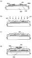
도 1a 내지 도 1e는 반도체 장치 및 상기 반도체 장치를 제작하기 위한 방법의 일 실시예를 도시한 도면.
도 2a 내지 도 2d는 반도체 장치 및 상기 반도체 장치를 제작하기 위한 방법의 일 실시예를 도시한 도면.
도 3a 내지 도 3e는 반도체 장치 및 상기 반도체 장치를 제작하기 위한 방법의 일 실시예를 도시한 도면.
도 4a 및 도 4b는 각각 반도체 장치의 일 실시예를 도시한 도면.
도 5a 내지 도 5d는 반도체 장치 및 상기 반도체 장치를 제작하기 위한 방법의 일 실시예를 도시한 도면.
도 6a 내지 도 6c는 각각 반도체 장치의 일 실시예를 도시한 도면.
도 7은 반도체 장치의 일 실시예를 도시한 도면.
도 8은 반도체 장치의 일 실시예를 도시한 도면.
도 9는 반도체 장치의 일 실시예를 도시한 도면.
도 10a 및 도 10b는 반도체 장치의 일 실시예를 도시한 도면.
도 11a 및 도 11b는 전자 기기를 도시한 도면.
도 12a 내지 도 12f는 각각 전자 기기를 도시한 도면.
도 13a 및 도 13b는 반도체 장치의 일 실시예를 도시한 도면.
도 14는 산소 도입 조건 하에서 산화물 반도체층의 시트 저항을 도시한 도면.1A to 1E are views showing one embodiment of a semiconductor device and a method for manufacturing the semiconductor device.
2A to 2D show an embodiment of a semiconductor device and a method for manufacturing the semiconductor device.
FIGS. 3A to 3E are views showing one embodiment of a semiconductor device and a method for manufacturing the semiconductor device. FIG.
4A and 4B show an embodiment of a semiconductor device, respectively.
5A to 5D show one embodiment of a semiconductor device and a method for manufacturing the semiconductor device.
6A to 6C each illustrate an embodiment of a semiconductor device.
7 illustrates one embodiment of a semiconductor device.
8 is a view showing an embodiment of a semiconductor device.
9 is a view showing an embodiment of a semiconductor device.
10A and 10B illustrate an embodiment of a semiconductor device.
11A and 11B are diagrams showing electronic devices.
12A to 12F are diagrams showing electronic devices, respectively.
13A and 13B illustrate an embodiment of a semiconductor device.
14 is a view showing sheet resistance of an oxide semiconductor layer under an oxygen introduction condition;
이하에서는, 본 발명의 실시예들이 첨부한 도면들을 참조하여 상세히 설명될 것이다. 그러나, 본 발명은 이하의 설명에 한정되지 않으며, 이 기술분야의 숙련자들에 의해 여기에 개시된 형태들 및 상세들이 다양한 방식들로 변경될 수 있다는 것이 쉽게 이해될 것이다. 또한, 본 발명은 이하에 도시된 실시예들에 대한 설명에 한정되는 것으로서 해석되지 않는다.Hereinafter, embodiments of the present invention will be described in detail with reference to the accompanying drawings. However, the present invention is not limited to the following description, and it will be readily understood by those skilled in the art that the forms and details disclosed herein may be altered in various ways. Further, the present invention is not construed as being limited to the description of the embodiments shown below.
(실시예 1)(Example 1)
이 실시예에서, 반도체 장치 및 상기 반도체 장치를 제작하기 위한 방법의 일 실시예가 도 1a 내지 도 1e를 참조하여 설명될 것이다. 이 실시예에서, 산화물 반도체층을 포함한 트랜지스터가 상기 반도체 장치의 일 예로서 도시된다.In this embodiment, one embodiment of a semiconductor device and a method for manufacturing the semiconductor device will be described with reference to Figs. 1A to 1E. In this embodiment, a transistor including an oxide semiconductor layer is shown as an example of the semiconductor device.
도 1e에 도시된 바와 같이, 트랜지스터(410)는 절연 표면을 가진 기판(400) 위에 형성되는, 게이트 전극층(401), 게이트 절연층(402), 산화물 반도체층(403), 소스 전극층(405a), 및 드레인 전극층(405b)을 포함한다. 산화물 절연층(407)(또한 제 1 절연층이라 불림) 및 보호 절연층(409)(또한 제 2 절연층이라 불림)이 이러한 순서로 상기 트랜지스터(410) 위에 적층된다.1E, the
도 1a 내지 도 1e는 상기 트랜지스터(410)를 제작하기 위한 방법의 일 예를 도시한다.FIGS. 1A through 1E show an example of a method for manufacturing the
먼저, 도전막이 절연 표면을 가진 상기 기판(400) 위에 형성되며, 그 후, 상기 게이트 전극층(401)이 제 1 포토리소그래피 단계에서 형성된다. 레지스트 마스크가 잉크젯 법에 의해 형성될 수 있다는 것을 주의하자. 잉크젯 법에 의한 상기 레지스트 마스크의 형성은 포토마스크를 필요로 하지 않으며; 따라서 제작 비용이 감소될 수 있다.First, a conductive film is formed on the
비록, 절연 표면을 가진 상기 기판(400)을 위해 사용된 기판에 대한 특별한 제한은 없지만, 바륨 보로실리케이트 유리, 알루미노보로실리케이트 유리 등의 유리 기판이 사용될 수 있다.Although there is no particular limitation on the substrate used for the
상기 반도체 장치는 상기 기판(400)으로서 가요성 기판을 사용하여 제작될 수 있다.The semiconductor device may be manufactured using the flexible substrate as the
가요성 반도체 장치를 제작하기 위해, 상기 산화물 반도체층(403)을 포함한 상기 트랜지스터(410)가 가요성 기판 위에 직접 제공될 수 있다. 대안적으로, 상기 산화물 반도체층(403)을 포함한 상기 트랜지스터(410)는 제작 기판 위에 제공되며, 그 후, 상기 트랜지스터(410)는 상기 제작 기판으로부터 분리되고 가요성 기판으로 이송된다. 상기 제작 기판으로부터 가요성 기판으로 분리 및 이송하기 위해, 분리층은 상기 제작 기판과 산화물 반도체층을 포함한 상기 트랜지스터 사이에 제공될 수 있다는 것을 주의하자.In order to fabricate a flexible semiconductor device, the
하지막(base film)으로서 작용하는 절연막은 상기 기판(400) 및 상기 게이트 전극층(401) 사이에 제공될 수 있다. 상기하지 막은 상기 기판(400)으로부터 불순물 소자의 확산을 방지하는 기능을 가지며, 질화 실리콘막, 산화 실리콘막, 질화 산화 실리콘막, 및 산질화 실리콘막 중 하나 이상을 사용한 단층 구조 또는 적층 구조를 갖고 형성될 수 있다.An insulating film serving as a base film may be provided between the
상기 게이트 전극층(401)은 몰리브덴, 티타늄, 탄탈, 텅스텐, 알루미늄, 구리, 네오디뮴, 또는 스칸듐과 같은 금속 재료, 또는 이들 재료들 중 임의의 것을 그것의 주성분으로서 포함하는 합금 재료를 사용한 단층 구조 또는 적층 구조를 갖도록 형성될 수 있다.The
다음으로, 상기 게이트 절연층(402)은 상기 게이트 전극층(401) 위에 형성된다. 상기 게이트 절연층(402)은 플라즈마 CVD법, 스퍼터링법 등에 의해 산화 실리콘층, 질화 실리콘층, 산질화 실리콘층, 질화 산화 실리콘층, 산화 알루미늄층, 질화 알루미늄층, 산질화 알루미늄층, 질화 산화 알루미늄층, 및 산화 하프늄층 중 임의의 것을 사용한 단층 구조 또는 적층 구조를 갖고 형성될 수 있다.Next, the
이 실시예에 사용된 상기 산화물 반도체는 불순물들이 제거되고 캐리어 공여체들로서 작용하고 상기 산화물 반도체층의 주성분 이외의 다른 물질들인 불순물들을 가능한 한 적게 포함하도록 고정제되는 진성(i-형) 또는 실질적으로 진성(i-형) 산화물 반도체이다.The oxide semiconductor used in this embodiment is an intrinsic (i-type) or substantially intrinsic (i-type) semiconductor that is a fixed agent to remove impurities and act as carrier donors and to contain as few impurities as possible other than the main component of the oxide semiconductor layer. (i-type) oxide semiconductor.
이러한 고정제된 산화물 반도체는 계면 준위 및 계면 전하에 매우 민감하며; 따라서, 상기 산화물 반도체층 및 상기 게이트 절연층 간의 계면은 중요하다. 이러한 이유로, 고정제된 산화물 반도체층과 접하는 상기 게이트 절연층은 높은 품질을 가질 필요가 있다.These immobilized oxide semiconductors are very sensitive to interfacial levels and interface charge; Therefore, the interface between the oxide semiconductor layer and the gate insulating layer is important. For this reason, the gate insulating layer in contact with the immobilized oxide semiconductor layer needs to have a high quality.
예를 들면, 치밀하고 높은 항복 전압 및 높은 품질을 가진 절연층이 획득될 수 있기 때문에 바람직하게는 마이크로파들(예로서, 2.45 GHz의 주파수)을 사용한 고-밀도 플라즈마 CVD법이 채택된다. 상기 고정제된 산화물 반도체 및 상기 고-품질 게이트 절연층은 서로 밀착되며, 그에 의해 상기 계면 준위 밀도는 양호한 계면 특성들을 획득하기 위해 저감될 수 있다.For example, a high-density plasma CVD process employing microwaves (e.g., a frequency of 2.45 GHz) is preferably employed because an insulating layer with dense, high breakdown voltage and high quality can be obtained. The immobilized oxide semiconductor and the high-quality gate insulating layer are in close contact with each other, whereby the interfacial level density can be reduced to obtain good interfacial properties.
말할 필요도 없이, 스퍼터링법 또는 플라즈마 CVD법과 같은 또 다른 막 형성 방법이, 상기 방법이 게이트 절연층으로서 양호한-품질의 절연층의 형성을 가능하게 하는 한 이용될 수 있다. 또한, 막 품질과 상기 절연층 및 산화물 반도체 간의 계면의 특성이 상기 절연층의 형성 후 수행된 열 처리에 의해 개선되는 절연층이 게이트 절연층으로서 형성될 수 있다. 어쨌든, 임의의 절연층이, 게이트 절연층으로서 양호한 막 품질을 가질 뿐만 아니라 상기 절연층 및 산화물 반도체 간의 상기 계면의 계면 준위 밀도에서의 감소 및 양호한 계면의 형성을 가능하게 하는 특성들을 갖는 한 사용될 수 있다.Needless to say, another film forming method such as a sputtering method or a plasma CVD method can be used as long as the above method enables formation of a good-quality insulating layer as a gate insulating layer. In addition, an insulating layer can be formed as a gate insulating layer in which the film quality and the characteristics of the interface between the insulating layer and the oxide semiconductor are improved by the heat treatment performed after the formation of the insulating layer. In any case, an optional insulating layer can be used as long as it has properties that not only have a good film quality as a gate insulating layer but also allow for a reduction in the interface level density of the interface between the insulating layer and the oxide semiconductor and formation of a good interface have.
수소, 수산기, 및 수분이 가능한 한 적게 상기 게이트 절연층(402) 및 상기 산화물 반도체층에 포함될 수 있도록, 그 위에 상기 게이트 전극층(401)이 형성되는 상기 기판(400) 또는 상기 게이트 절연층(402)까지 층들이 형성되는 상기 기판(400)이 상기 기판(400)에 흡수된 수소 및 수분과 같은 불순물들이 제거되고 배기되도록 상기 산화물 반도체층의 막 형성을 위한 사전 처리로서 스퍼터링 장치의 예열실(preheating chamber)에서 예열되는 것이 바람직하다. 상기 예열실에 제공된 배기 수단으로서, 크라이오펌프가 바람직하다. 이러한 예열실은 생략될 수 있다는 것을 주의하자. 이러한 예열은 상기 산화물 절연층(407)의 형성 전에, 유사하게는 그 위에 소스 전극층(405a) 및 드레인 전극층(405b)까지의 층들이 형성되는 상기 기판(500) 상에서 수행될 수 있다.The
다음으로, 상기 게이트 절연층(402) 위에, 2 nm 이상 200 nm 이하, 바람직하게는 5 nm 이상 30 nm 이하의 두께를 가진 산화물 반도체층이 형성된다.Next, an oxide semiconductor layer having a thickness of 2 nm or more and 200 nm or less, preferably 5 nm or more and 30 nm or less, is formed on the
상기 산화물 반도체층이 스퍼터링법에 의해 형성되기 전에, 막 형성시 생성되고 상기 게이트 절연층(402)의 표면상에 부착된 가루 물질들(또한 입자들 또는 먼지라 불림)이 바람직하게는 아르곤 가스가 도입되고 플라즈마가 생성되는 역 스퍼터링에 의해 제거된다. 상기 역 스퍼터링은 기판 표면이 변경되도록 전압이 RF 전원을 사용함으로써 아르곤 분위기 하에서 타겟 측이 아닌, 기판 측에 인가되고, 상기 기판의 부근에 플라즈마가 생성되는 방법이다. 아르곤 분위기 대신에, 질소 분위기, 헬륨 분위기, 산소 분위기 등이 사용될 수 있다는 것을 주의하자.Before the oxide semiconductor layer is formed by the sputtering method, the powdery materials (also called particles or dust) generated at the time of film formation and adhered on the surface of the
상기 산화물 반도체층을 위해 사용된 산화물 반도체로서, In-Sn-Ga-Zn-O계 산화물 반도체와 같은 4-원계 금속 산화물; In-Ga-Zn-O계 산화물 반도체, In-Sn-Zn-O계 산화물 반도체, In-Al-Zn-O계 산화물 반도체, Sn-Ga-Zn-O계 산화물 반도체, Al-Ga-Zn-O계 산화물 반도체, 또는 Sn-Al-Zn-O계 산화물 반도체와 같은 3-원계 금속 산화물; In-Zn-O계 산화물 반도체, Sn-Zn-O계 산화물 반도체, Al-Zn-O계 산화물 반도체, Zn-Mg-O계 산화물 반도체, Sn-Mg-O계 산화물 반도체, 또는 In-Mg-O계 산화물 반도체와 같은 2-원계 금속 산화물; In-O계 산화물 반도체; Sn-O계 산화물 반도체; 또는 Zn-O계 산화물 반도체가 사용될 수 있다. 또한, SiO2가 상기 산화물 반도체에 포함될 수 있다. 여기에서, 예를 들면, In-Ga-Zn-O계 산화물 반도체는 인듐(In), 갈륨(Ga), 및 아연(Zn)을 의미하며, 그 화학량론적 비에 대한 특별한 제한은 없다는 것을 주의하자. 더욱이, 상기 In-Ga-Zn-O계 산화물 반도체는 In, Ga, 및 Zn 이외의 다른 원소를 포함할 수 있다.As the oxide semiconductor used for the oxide semiconductor layer, a 4-element metal oxide such as an In-Sn-Ga-Zn-O-based oxide semiconductor; In-Zn-O-based oxide semiconductor, In-Sn-Zn-O-based oxide semiconductor, In-Sn-Zn- O-based oxide semiconductor, or a Sn-Al-Zn-O-based oxide semiconductor; Mg-O based oxide semiconductor, Sn-Zn-O based oxide semiconductor, Sn-Zn-O based oxide semiconductor, Al-Zn-O based oxide semiconductor, Zn- O-based oxide semiconductors; In-O-based oxide semiconductor; Sn-O-based oxide semiconductor; Or a Zn-O-based oxide semiconductor may be used. Further, SiO2 may be included in the oxide semiconductor. Note that, for example, the In-Ga-Zn-O-based oxide semiconductor means indium (In), gallium (Ga), and zinc (Zn), and there is no particular limitation on the stoichiometric ratio . Further, the In-Ga-Zn-O-based oxide semiconductor may include other elements than In, Ga, and Zn.
상기 산화물 반도체층을 위해, InMO3(ZnO)m(m>0, 및 m은 자연수가 아니다)에 의해 표현된 박막이 사용될 수 있다. 여기에서, M은 Ga, Al, Mn, 및 Co로부터 선택된 하나 이상의 금속 원소들을 나타낸다. 예를 들면, M은 Ga, Ga와 Al, Ga와 Mn, Ga와 Co 등일 수 있다.For the oxide semiconductor layer, a thin film represented by InMO3 (ZnO)m (m> 0, and m is not a natural number) may be used. Here, M represents one or more metal elements selected from Ga, Al, Mn, and Co. For example, M may be Ga, Ga and Al, Ga and Mn, Ga and Co, and the like.
이 실시예에서, 상기 산화물 반도체층은 스퍼터링법에 의해 In-Ga-Zn-O계 금속 산화물 타겟을 사용하여 형성된다. 또한, 상기 산화물 반도체층은 희가스(대표적으로, 아르곤) 분위기, 산소 분위기, 또는 희가스 및 산소의 혼합 분위기 하에서 스퍼터링법에 의해 형성될 수 있다.In this embodiment, the oxide semiconductor layer is formed using an In-Ga-Zn-O-based metal oxide target by a sputtering method. The oxide semiconductor layer may be formed by a sputtering method in a rare gas (typically argon) atmosphere, an oxygen atmosphere, or a mixed atmosphere of rare gas and oxygen.
스퍼터링법에 의해 상기 산화물 반도체층의 형성을 위해 사용된 상기 타겟은 예를 들면, In2O3:Ga2O3:ZnO = 1:1:1 [몰 비]의 조성비를 가진 금속 산화물 타겟이며, 따라서, In-Ga-Zn-O 막이 형성된다. 상기 재료 및 상기 타겟의 구성요소에 대한 제한 없이, 예를 들면, In2O3:Ga2O3:ZnO = 1:1:2 [몰 비]의 조성비를 가진 금속 산화물 타겟이 사용될 수 있다.The target used for forming the oxide semiconductor layer by the sputtering method is a metal oxide target having a composition ratio of, for example, In2 O3 : Ga2 O3 : ZnO = 1: 1: 1 [molar ratio] , And thus an In-Ga-Zn-O film is formed. A metal oxide target having a composition ratio of, for example, In2 O3 : Ga2 O3 : ZnO = 1: 1: 2 [molar ratio] may be used without limitation to the material and the target component.
상기 금속 산화물 타겟의 충전율(fill rate)은 90% 이상 100% 이하, 바람직하게는 95% 이상 99.9% 이하이다. 높은 충전율을 가진 금속 산화물 타겟을 사용하여, 상기 형성된 산화물 반도체층은 높은 밀도를 가질 수 있다. The fill rate of the metal oxide target is 90% or more and 100% or less, preferably 95% or more and 99.9% or less. Using a metal oxide target having a high filling rate, the oxide semiconductor layer formed may have a high density.
산화물 반도체층이 형성될 때 사용된 스퍼터링 가스로서 수소, 물, 수산기, 또는 수소화물과 같은 불순물들이 제거되는 고-순도 가스를 사용하는 것이 바람직하다.It is preferable to use a high-purity gas in which impurities such as hydrogen, water, hydroxyl groups, or hydrides are removed as the sputtering gas used when the oxide semiconductor layer is formed.
상기 기판은 감압하에서 성막실(film formation chamber)에 위치되며 상기 기판 온도는 100℃ 이상 600℃ 이하, 바람직하게는 200℃ 이상 400℃ 이하로 설정된다. 막 형성 동안 상기 기판을 가열함으로써, 형성된 상기 산화물 반도체층에 포함된 불순물들의 농도는 저감될 수 있다. 또한, 스퍼터링에 의한 손상이 감소될 수 있다. 그 후, 수소 및 수분이 제거되는 스퍼터링 가스가 그 안에 남아있는 수분이 제거되는 동안 상기 성막실로 도입되며, 상기 산화물 반도체층은 상기 타겟의 사용으로 상기 기판(400) 위에 형성된다. 상기 성막실에서 남아있는 수분을 제거하기 위해, 흡착형 진공 펌프(entrapment vacuum pump), 예를 들면, 크라이오펌프, 이온 펌프, 또는 티타늄 승화 펌프(titanium sublimation pump)가 사용되는 것이 바람직하다. 배기 수단으로서, 콜드 트랩이 부가되는 터보 분자 펌프가 사용될 수 있다. 상기 크라이오펌프를 갖고 배기되는 상기 성막실에서, 수소 원자, 물(H2O)과 같이 수소 원자를 포함한 화합물(보다 바람직하게는, 또한 탄소 원자를 포함한 화합물) 등이 배기되며, 그에 의해 상기 성막실에 형성된 상기 산화물 반도체층에 포함된 불순물들의 농도는 저감될 수 있다.The substrate is placed in a film formation chamber under a reduced pressure, and the substrate temperature is set at 100 ° C or more and 600 ° C or less, preferably 200 ° C or more and 400 ° C or less. By heating the substrate during film formation, the concentration of the impurities contained in the formed oxide semiconductor layer can be reduced. In addition, damage due to sputtering can be reduced. Thereafter, hydrogen and moisture-removed sputtering gas is introduced into the deposition chamber while moisture remaining therein is removed, and the oxide semiconductor layer is formed on the
상기 성막 조건의 일 예로서, 상기 기판 및 상기 타겟 간의 거리는 100 mm이고, 상기 압력은 0.6 Pa이고, 직류(DC) 전원은 0.5 kW이며, 상기 분위기는 산소 분위기(산소 유량 비율은 100%이다)이다. 펄스 직류 전원은 상기 성막 시 생성된 가루 물질들(또한 입자들 또는 먼지라 불림)이 감소될 수 있고 상기 막 두께가 균일할 수 있기 때문에 바람직하다는 것을 주의하자.As an example of the film formation conditions, the distance between the substrate and the target is 100 mm, the pressure is 0.6 Pa, the direct current (DC) power source is 0.5 kW, the atmosphere is oxygen atmosphere (oxygen flow rate is 100% to be. It should be noted that the pulsed direct current power supply is preferable because the powdery materials (also called particles or dust) generated during the film formation can be reduced and the film thickness can be uniform.
다음으로, 제 2 포토리소그래피 단계에서, 상기 산화물 반도체층은 섬형상 산화물 반도체층(441)으로 가공된다(도 1a 참조). 상기 섬형상 산화물 반도체층(441)을 형성하기 위한 레지스트 마스크가 잉크젯 법을 사용하여 형성될 수 있다. 잉크젯 법에 의한 상기 레지스트 마스크의 형성은 포토마스크를 필요로 하지 않으며; 따라서 제작 비용이 감소될 수 있다.Next, in the second photolithography step, the oxide semiconductor layer is processed into an island-shaped oxide semiconductor layer 441 (see FIG. 1A). A resist mask for forming the island-like
콘택트 홀(contact hole)이 상기 게이트 절연층(402)에 형성되는 경우에, 상기 콘택트 홀을 형성하는 단계는 상기 산화물 반도체층(441)의 가공과 동일한 시간에 수행될 수 있다.In the case where a contact hole is formed in the
상기 산화물 반도체층의 에칭은 드라이 에칭, 웨트 에칭, 또는 드라이 에칭 및 웨트 에칭 모두일 수 있다는 것을 주의하자. 상기 산화물 반도체층의 웨트 에칭을 위한 에천트로서, 예를 들면, 인산, 아세트산, 및 질산을 혼합함으로써 획득된 용액, 암모니아과수(31 wt%에서의 과산화수소수: 28 wt%에서의 암모니아수: 물 = 5:2:2) 등이 사용될 수 있다. 또한, ITO07N(칸토 케미칼 코., 인크.(KANTO CHEMICAL CO., INC.)에 의해 제조)이 또한 사용될 수 있다.Note that the etching of the oxide semiconductor layer may be both dry etching, wet etching, or both dry etching and wet etching. A solution obtained by mixing phosphoric acid, acetic acid, and nitric acid as an etchant for wet etching the oxide semiconductor layer, ammonia and water (aqueous hydrogen peroxide at 31 wt%: ammonia water at 28 wt%: water = 5: 2: 2) may be used. ITO07N (manufactured by KANTO CHEMICAL CO., INC.) May also be used.
다음으로, 소스 전극층 및 드레인 전극층(상기 소스 전극층 및 상기 드레인 전극층과 동일한 층에 형성된 배선을 포함)이 되도록 도전막이 상기 게이트 절연층(402) 및 상기 산화물 반도체층(441) 위에 형성된다. 상기 소스 전극층 및 상기 드레인 전극층을 위해 사용된 도전막으로서, 예를 들면, Al, Cr, Cu, Ta, Ti, Mo, 및 W로부터 선택된 원소를 포함한 금속막 및 상기 원소들 중 임의의 것을 그것의 주성분으로서 포함하는 금속 질화물 막(질화 티타늄막, 질화 몰리브덴 막, 및 질화 텅스텐막)이 사용될 수 있다. Ti, Mo, W 등의 높은 용해점을 가진 금속막 또는 이들 원소들 중 임의의 것의 금속 질화물 막(질화 티타늄막, 질화 몰리브덴 막, 및 질화 텅스텐막)이 Al, Cu 등의 금속막의 하부 측 또는 상부 측 중 하나 또는 둘 모두 상에 적층될 수 있다. 대안적으로, 상기 소스 전극층 및 상기 드레인 전극층이 될 상기 도전막은 도전성 금속 산화물을 사용하여 형성될 수 있다. 도전성 금속 산화물로서, 산화 인듐(In2O3), 산화 주석(SnO2), 산화 아연(ZnO), 산화 인듐 및 산화 주석의 합금(In2O3-SnO2, ITO로서 약칭됨), 산화 인듐 및 산화 아연의 합금(In2O3-ZnO), 또는 산화 실리콘이 포함되는 이들 금속 산화물 재료들 중 임의의 것이 사용될 수 있다.Next, a conductive film is formed on the
레지스트 마스크는 제 3 포토리소그래피 단계에 의해 상기 도전막 위에 형성된다. 에칭은 선택적으로 수행되며, 따라서 상기 소스 전극층(405a) 및 상기 드레인 전극층(405b)이 형성된다. 그 후, 상기 레지스트 마스크가 제거된다.A resist mask is formed on the conductive film by a third photolithography step. Etching is selectively performed, so that the
상기 제 3 포토리소그래피 단계에서 상기 레지스트 마스크의 형성시 노광은 자외선 광, KrF 레이저 광, 또는 ArF 레이저 광을 사용하여 수행될 수 있다. 나중에 형성된 상기 트랜지스터의 채널 길이(L)는 상기 산화물 반도체층(441) 위에서 서로 이웃하는 상기 소스 전극층의 하단부 및 상기 드레인 전극층의 하단부 사이의 거리에 의해 결정된다. 노광이 25 nm 미만의 채널 길이(L)를 위해 수행되는 경우에, 상기 제 3 포토리소그래피 단계에서 상기 레지스트 마스크의 형성시 상기 노광은 수 나노미터들 내지 수십 나노미터들의 매우 짧은 파장을 가진 극자외선 광을 사용하여 수행될 수 있다. 극자외선 광에 의한 상기 노광에서, 상기 해상도는 높으며 초점 심도는 크다. 결과적으로, 나중에 형성될 상기 트랜지스터의 채널 길이(L)는 10 nm 내지 1000 nm일 수 있으며, 그에 의해 회로의 동작 속도는 증가될 수 있다.The exposure in forming the resist mask in the third photolithography step may be performed using ultraviolet light, KrF laser light, or ArF laser light. The channel length L of the transistor formed later is determined by the distance between the lower end of the source electrode layer and the lower end of the drain electrode layer adjacent to each other on the
포토리소그래피 단계에서 사용된 포토마스크들의 수를 감소시키고 포토리소그래피 단계들의 수를 감소시키기 위해, 에칭 단계가 복수의 강도들을 갖도록 광이 투과되는 노광 마스크인 다계조 마스크(multi-tone mask)를 사용하여 수행될 수 있다. 다계조 마스크를 사용하여 형성된 레지스트 마스크는 복수의 두께들을 가지며 또한 에칭에 의해 형상이 변경될 수 있으며; 그러므로, 상기 레지스트 마스크는 상이한 패턴들로 처리하기 위한 복수의 에칭 단계들에서 사용될 수 있다. 그러므로, 적어도 두 종류 이상의 상이한 패턴들에 대응하는 레지스트 마스크가 하나의 다계조 마스크에 의해 형성될 수 있다. 따라서, 노광 마스크들의 수는 감소될 수 있고 대응하는 포토리소그래피 단계들의 수가 또한 감소될 수 있으며, 그에 의해 프로세스의 간략화가 실현될 수 있다.In order to reduce the number of photomasks used in the photolithography step and to reduce the number of photolithography steps, a multi-tone mask, which is an exposure mask through which light is transmitted such that the etching step has a plurality of intensities . A resist mask formed using a multi-gradation mask has a plurality of thicknesses and can be changed in shape by etching; Therefore, the resist mask can be used in a plurality of etching steps for processing with different patterns. Therefore, a resist mask corresponding to at least two or more different patterns can be formed by one multi-gradation mask. Thus, the number of exposure masks can be reduced and the number of corresponding photolithography steps can also be reduced, thereby simplifying the process can be realized.
에칭 조건들은 상기 도전막이 에칭될 때 상기 산화물 반도체층(441)을 에칭하고 분할하지 않도록 최적화되는 것이 바람직하다는 것을 주의하자. 그러나, 단지 상기 도전막이 에칭되고 상기 산화물 반도체층(441)이 전혀 에칭되지 않는 에칭 조건들을 획득하는 것은 어려우며; 몇몇 경우들에서, 단지 상기 산화물 반도체층(441)의 일부만이 홈부(오목부)가 되도록 상기 도전막의 에칭에 의해 에칭된다.Note that the etching conditions are preferably optimized to etch and not divide the
이 실시예에서, Ti 막이 상기 도전막으로서 사용되고 상기 In-Ga-Zn-O계 산화물 반도체가 상기 산화물 반도체층(441)을 위해 사용되기 때문에, 암모니아과수(암모니아 수, 물, 및 과산화수소수의 혼합액)가 에칭액으로서 사용된다.In this embodiment, since the Ti film is used as the conductive film and the In-Ga-Zn-O-based oxide semiconductor is used for the
다음으로, N2O, N2, 또는 Ar과 같은 가스를 사용한 플라즈마 처리에 의해, 상기 산화물 반도체층(441)의 노출된 부분의 표면에 흡수된 물 등이 제거될 수 있다. 상기 플라즈마 처리가 수행되는 경우에, 상기 산화물 반도체층(441)의 일부와 접하는 상기 산화물 절연층(407)이 공기에 노출되지 않고 형성된다.Next, by the plasma treatment using a gas such as N2 O, N2 , or Ar, water or the like absorbed on the surface of the exposed portion of the
상기 산화물 절연층(407)은 적어도 1 nm 이상의 두께를 가지며 스퍼터링법과 같이, 물 및 수소와 같은 불순물들이 상기 산화물 절연층(407)에 포함되지 않는 방법에 의해 적절하게 형성될 수 있다. 수소가 상기 산화물 절연층(407)에 포함될 때, 상기 산화물 반도체층으로의 상기 수소의 진입 또는 상기 수소에 의한 상기 산화물 반도체층에서의 산소의 추출이 야기되며, 그에 의해 상기 산화물 반도체층의 백채널의 저항이 낮아지고(n-형 도전성을 갖도록), 따라서 기생 채널이 형성될 수 있다. 그러므로, 수소가 사용되지 않는 형성 방법이 상기 산화물 절연층(407)이 수소를 가능한 한 적게 포함하도록 이용된다는 것이 중요하다.The
상기 산화물 절연층(407)을 위해, 대표적으로, 산화 실리콘막 또는 산질화 실리콘막과 같은 무기 절연막이 사용될 수 있다.For the
이 실시예에서, 상기 산화물 절연층(407)으로서, 200 nm의 두께를 가진 산화 실리콘막이 스퍼터링법에 의해 형성된다. 막 형성에서 기판 온도는 실온 이상 300℃ 이하일 수 있으며 이 실시예에서는 100℃이다. 상기 산화 실리콘막은 희가스(대표적으로, 아르곤) 분위기, 산소 분위기, 또는 희가스 및 산소를 포함한 혼합 분위기 하에서 스퍼터링법에 의해 형성될 수 있다. 타겟으로서, 산화 실리콘 타겟 또는 실리콘 타겟이 사용될 수 있다. 예를 들면, 상기 산화 실리콘막이 산소를 포함한 분위기에서 스퍼터링법에 의해 실리콘 타겟을 사용하여 형성될 수 있다.In this embodiment, as the
상기 산화물 반도체층의 막 형성과 동시에 상기 산화물 절연층(407)의 성막실에 남아있는 수분을 제거하기 위해, 바람직하게는 흡착형 진공 펌프(크라이오펌프와 같은)가 사용된다. 크라이오펌프가 상기 성막실을 배기하기 위해 형성될 때, 상기 산화물 절연층(407)에 포함된 불순물들의 농도는 감소될 수 있다. 또한, 상기 산화물 절연층(407)의 상기 성막실에 남아있는 수분을 제거하기 위한 배기 수단으로서, 콜드 트랩을 갖춘 터보 분자 펌프가 사용될 수 있다.In order to remove moisture remaining in the deposition chamber of the
수소, 물, 수산기, 또는 수소화물과 같은 불순물들이 제거되는 고-순도 가스가 바람직하게는 상기 산화물 절연층(407)의 형성에 사용된 스퍼터링 가스로서 사용된다.A high-purity gas from which impurities such as hydrogen, water, hydroxyl, or hydride are removed is preferably used as the sputtering gas used in forming the
다음으로, 산소(421)가 상기 산화물 절연층(407)을 통해 상기 산화물 반도체층(441)에 도입된다(도 1c 참조).Next,
상기 산소(421)를 도입하기 위한 방법으로서, 이온 주입법, 이온 도핑법 등이 사용될 수 있다. 이온 주입법에서, 소스 가스가 플라즈마화되며, 이러한 플라즈마에 포함된 이온종들이 추출되고 질량 분리되며, 미리 결정된 질량을 가진 이온종들이 가속되며 이온 빔으로서 피처리물에 주입된다. 이온 도핑법에서, 소스 가스는 플라즈마화되며, 이온종들이 미리 결정된 전계의 동작에 의해 이 플라즈마로부터 추출되며, 상기 추출된 이온종들은 질량 분리 없이 가속되고 이온 빔으로서 피처리물에 주입된다. 산소의 도입이 질량 분리를 수반한 이온 주입법을 사용하여 수행될 때, 금속 원소와 같은 불순물이 상기 산화물 반도체층으로 첨가되는 것을 방지할 수 있다. 또한, 이온 도핑법은 이온 주입법보다 큰 영역으로의 이온-빔 조사를 가능하게 하며; 그러므로, 산소의 첨가가 이온 도핑법을 사용하여 수행될 때, 택 타임(takt time)은 단축될 수 있다.As a method for introducing the
산소가 상기 산화물 반도체층(441) 위에 적층된 상기 산화물 절연층(407)을 통해 상기 산화물 반도체층(441)에 도입되며, 따라서 산소가 도입되는 도입 깊이(도입 영역)는 제어될 수 있고 따라서 산소가 상기 산화물 반도체층(441)에 충분히 도입될 수 있다. 산소가 도입되는 상기 깊이는 가속 전압 및 도즈량(dose)과 같은 도입 조건 또는 상기 산소가 통과하는 산화물 절연층의 두께를 적절히 설정함으로써 제어될 수 있다. 산소 가스가 사용되고 산소가 이온 주입법에 의해 도입되는 경우에, 상기 도즈량은 1×10¹³ 이온/㎠ 이상 5×10¹⁵ 이온/㎠ 이하의 범위에서 설정될 수 있다.Oxygen is introduced into the
특히, 산화물 반도체층의 채널 형성 영역에 수소, 물, 수산기, 또는 수소화물과 같은 불순물들을 제거하는 것이 중요하며, 따라서 보텀-게이트 구조를 가진 상기 트랜지스터(410)에서, 많은 양의 산소가 바람직하게는 상기 산화물 반도체층(441)에서 상기 게이트 절연층(402)과의 계면의 부근에 도입된다.In particular, it is important to remove impurities such as hydrogen, water, hydroxyl, or hydride in the channel forming region of the oxide semiconductor layer, and thus, in the
상기 산화물 반도체층에서 상기 도입된 산소 농도의 피크는 1×10¹⁸ /㎤ 내지 3×10²⁰ /㎤(보다 바람직하게는, 1×10¹⁸ /㎤ 내지 1×10²⁰ /㎤)인 것이 바람직하다.The peak of the introduced oxygen concentration in the oxide semiconductor layer is preferably 1 × 10¹⁸ / cm 3 to 3 × 10²⁰ / cm 3 (more preferably 1 × 10¹⁸ / cm 3 to 1 × 10²⁰ / cm 3) .
상술된 산소 농도는 다음 방식으로 측정될 수 있다: 질량수 18의 산소 동위원소가 산소로서 도입되며, 상기 도입 후, 상기 산화물 반도체층에서의 상기 질량 수 18의 산소 동위 원소의 농도는 2차 이온 질량 분석법(secondary ion mass spectroscopy; SIMS)에 의해 분석된다.The oxygen concentration described above can be measured in the following manner: the oxygen isotope of mass number 18 is introduced as oxygen, and after the introduction, the concentration of the oxygen isotope of the mass number 18 in the oxide semiconductor layer is the secondary ion mass Analysis by secondary ion mass spectroscopy (SIMS).
다음으로, 산소가 도입되고 그 일부(채널 형성 영역)가 상기 산화물 절연층(407)과 접하는 상기 산화물 반도체층(441)이 열 처리된다.Next, the
상기 열 처리의 온도는 250℃ 이상 700℃ 이하, 바람직하게는 400℃ 이상 700℃ 이하, 또는 상기 기판의 변형점 미만이다. 예를 들면, 상기 기판이 열 처리 장치의 한 종류인 전기로에 넣어진 후, 상기 산화물 반도체층(441)은 질소 분위기에서 1시간 동안 450℃에서 상기 열 처리를 겪는다.The temperature of the heat treatment is not less than 250 ° C and not more than 700 ° C, preferably not less than 400 ° C and not more than 700 ° C, or less than the strain point of the substrate. For example, after the substrate is placed in an electric furnace which is a kind of a heat treatment apparatus, the
사용된 열 처리 장치는 전기로에 한정되지 않으며, 저항 발열체와 같은 가열 소자로부터 열 도전 또는 열 복사에 의해 피처리물을 가열하기 위한 장치가 대안적으로 사용될 수 있다는 것을 주의하자. 예를 들면, 가스 급속 열 어닐(GRTA) 장치 또는 램프 급속 열 어닐(LRTA) 장치와 같은 급속 열 어닐(RTA) 장치가 사용될 수 있다. LRTA 장치는 할로겐 램프, 메탈 할라이드 램크, 크세논 아크 램프, 탄소 아크 램프, 고압 나트륨 램프, 또는 고압 수은 램프와 같은 램프로부터 방출된 광(전자기파)의 복사에 의해 피처리물을 가열하기 위한 장치이다. GRTA 장치는 고온 가스를 사용한 열 처리를 위한 장치이다. 상기 고온 가스로서, 질소 또는 희가스와 같이, 열 처리에 의해 피처리물과 반응하지 않는 불활성 가스가 사용된다.It should be noted that the heat treatment apparatus used is not limited to an electric furnace, and an apparatus for heating the object to be treated by thermal conduction or heat radiation from a heating element such as a resistance heating body may alternatively be used. For example, a rapid thermal anneal (RTA) device such as a gas rapid thermal anneal (GRTA) device or a lamp rapid thermal anneal (LRTA) device may be used. The LRTA device is a device for heating an object to be processed by radiation of light (electromagnetic waves) emitted from a lamp such as a halogen lamp, a metal halide lamp, a xenon arc lamp, a carbon arc lamp, a high pressure sodium lamp, or a high pressure mercury lamp. The GRTA device is a device for heat treatment using hot gases. As the high-temperature gas, an inert gas which does not react with the object to be treated by heat treatment such as nitrogen or a rare gas is used.
예를 들면, 상기 열 처리로서, GRTA가 다음과 같이 수행될 수 있다. 상기 기판은 650℃ 내지 700℃의 고온에서 가열된 불활성 가스에 넣어지고, 수분 동안 가열되며, 상기 불활성 가스로부터 꺼내어진다.For example, as the heat treatment, GRTA can be performed as follows. The substrate is placed in an inert gas heated at a high temperature of 650 ° C to 700 ° C, heated for a few minutes, and taken out of the inert gas.
상기 열 처리가 질소, 산소, 초-건조 공기(물 함유량이 20 ppm 이하, 바람직하게는 1 ppm 이하, 보다 바람직하게는 10 ppb 이하인 공기), 또는 희가스(아르곤, 헬륨 등)의 분위기 하에서 수행될 수 있다. 물, 수소 등이 질소, 산소, 초-건조 공기, 또는 희가스의 분위기에 포함되지 않는 것이 바람직하다는 것을 주의하자. 열 처리 장치로 도입되는 질소, 산소, 또는 희가스의 순도는 6N(99.9999%) 이상, 바람직하게는 7N(99.99999%) 이상(즉, 불순물 농도는 1 ppm 이하, 바람직하게는 0.1 ppm 이하)로 설정되는 것이 또한 바람직하다.The heat treatment may be carried out in an atmosphere of nitrogen, oxygen, super-dry air (water having a water content of 20 ppm or less, preferably 1 ppm or less, more preferably 10 ppb or less), or rare gas (argon, helium, etc.) . It is preferable that water, hydrogen, and the like are not included in the atmosphere of nitrogen, oxygen, super-dry air, or rare gas. The purity of nitrogen, oxygen, or rare gas introduced into the heat treatment apparatus is set to 6N (99.9999%) or more, preferably 7N (99.99999%) or more (i.e., the impurity concentration is 1 ppm or less, preferably 0.1 ppm or less) .
상기 산소의 도입에 의해, 상기 산화물 반도체에 포함된 금속 및 수소 사이의 결합 또는 상기 금속 및 수산기 사이의 결합이 절단된다. 동시에, 상기 수소 또는 상기 수산기는 물을 생성하기 위해 산소와 반응한다. 결과적으로, 불순물인 수소 또는 수산기는 나중에 수행된 상기 열 처리에 의해 물로서 쉽게 제거될 수 있다.By the introduction of the oxygen, the bond between the metal and hydrogen contained in the oxide semiconductor or the bond between the metal and the hydroxyl group is cleaved. At the same time, the hydrogen or the hydroxyl reacts with oxygen to produce water. As a result, impurities such as hydrogen or hydroxyl groups can be easily removed as water by the heat treatment performed later.
상기 산소의 도입 및 상기 열 처리에 의해, 상기 산화물 반도체층은 탈수화 또는 탈수소화될 수 있으며, 그에 의해 수소, 물, 수산기, 또는 수소화물과 같은 불순물들이 상기 산화물 반도체층으로부터 제거될 수 있다.By the introduction of oxygen and the heat treatment, the oxide semiconductor layer can be dehydrated or dehydrogenated, whereby impurities such as hydrogen, water, hydroxyl groups, or hydrides can be removed from the oxide semiconductor layer.
상기 산화물 반도체층(441) 및 산소를 포함한 상기 산화물 절연층(407)은 열 처리될 때 서로 접하며; 따라서, 상기 산화물 반도체층(441)의 주성분 중 하나이고 불순물들을 제거하는 단계에서 감소되는 산소가 산소를 포함한 상기 산화물 절연층(407)으로부터 상기 산화물 반도체층(441)으로 공급될 수 있다. 상기 공정을 통해, 상기 산화물 반도체층(441)은 고정제되며, 따라서 상기 전기적으로 i-형(진성) 산화물 반도체층(403)이 획득된다.The
상기 고정제된 산화물 반도체층(403)에서의 캐리어들의 수는 매우 작으며(0에 가까운), 상기 캐리어 농도는 1×10¹⁴ /㎤ 미만, 바람직하게는 1×10¹² /㎤ 미만, 더 바람직하게는 1×10¹¹ /㎤ 미만이다.The number of carriers in the immobilized
상기 공정을 통해, 상기 트랜지스터(410)가 형성된다(도 1d 참조). 상기 트랜지스터(410)는 고정제되고 그로부터 수소, 수분, 수산기, 또는 수소화물(또한 수소 화합물이라 불림)과 같은 불순물들이 의도적으로 제거되는 상기 산화물 반도체층(403)을 포함한 트랜지스터이다. 그러므로, 상기 트랜지스터(410)의 전기적 특성들에서의 변화가 억제되며 상기 트랜지스터(410)는 전기적으로 안정된다.Through the above process, the
수분 또는 수소와 같은 불순물들이 외부로부터 들어오는 것을 방지하는 상기 보호 절연층(409)이 바람직하게는 이들 불순물들이 상기 산화물 반도체층(403)에 다시 포함되지 않도록 상기 산화물 절연층(407) 위에 형성된다(도 1e 참조). 무기 절연막이 상기 보호 절연층(409)을 위해 사용되며, 질화 실리콘막, 산화 알루미늄 막 등이 사용될 수 있다. 예를 들면, 질화 실리콘막이 RF 스퍼터링법에 의해 형성된다. RF 스퍼터링법은 높은 양산성을 가지므로, 상기 보호 절연층(409)의 막 형성 방법으로서 사용되는 것이 바람직하다.The
열 처리가 상기 보호 절연층(409)이 형성된 후 수행될 수 있다. 예를 들면, 상기 열 처리는 대기중에서 100℃ 이상 200℃ 이하로 1시간 이상 30시간 이하 동안 수행될 수 있다. 이러한 열 처리는 고정된 가열 온도에서 수행될 수 있다. 대안적으로, 가열 온도에서의 다음의 변화가 복수 회 반복적으로 행해질 수 있다: 상기 가열 온도는 실온에서 100℃ 이상 200℃ 이하의 온도로 증가되며 그 후 실온으로 감소된다.The heat treatment may be performed after the protective insulating
이 실시예에서 제작된 상기 고정제된 산화물 반도체층(403)을 사용한 상기 트랜지스터(410)에서, 채널 폭에서 마이크로미터당 오프 상태에서의 전류(오프-상태 전류 값)는 실온에서 10 zA/㎛ 미만, 85℃에서 100zA/㎛ 미만으로 감소될 수 있다.In the
또한, 상기 산화물 반도체층(403)을 포함한 상기 트랜지스터(410)의 전계-효과 이동도는 비교적 높을 수 있으며, 그에 의해 고-속 동작이 가능하다. 예를 들면, 고속으로 동작할 수 있는 이러한 트랜지스터가 액정 표시 장치를 위해 사용될 때, 화소부에서의 스위칭 트랜지스터 및 구동 회로부에서의 구동기 트랜지스터가 하나의 기판 위에 형성될 수 있다. 즉, 실리콘 웨이퍼 등으로 형성된 반도체 장치가 부가적으로 구동 회로로서 요구되지 않기 때문에, 상기 반도체 장치의 구성요소들의 수는 감소될 수 있다. 또한, 화소부에서 고속으로 동작할 수 있는 트랜지스터를 사용함으로써, 고-품질 이미지가 제공될 수 있다.In addition, the field-effect mobility of the
상술된 바와 같이, 안정된 전기적 특성들을 가진 산화물 반도체를 포함한 반도체 장치가 제공될 수 있다. 그러므로, 높은 신뢰성을 가진 반도체 장치가 제공될 수 있다.As described above, a semiconductor device including an oxide semiconductor having stable electrical characteristics can be provided. Therefore, a semiconductor device with high reliability can be provided.
(실시예 2)(Example 2)
이 실시예에서, 반도체 장치 및 상기 반도체 장치를 제작하기 위한 방법의 또 다른 실시예가 도 2a 내지 도 2d를 참조하여 설명될 것이다. 상기 실시예에서의 것들과 동일한 부분 또는 그것과 유사한 기능을 가진 부분은 상기 실시예에 설명된 것과 유사한 방식으로 형성될 수 있고, 또한 상기 실시예에서의 것들과 유사한 단계들이 상기 실시예에서 설명된 것과 유사한 방식으로 수행될 수 있으며, 반복적인 설명은 생략된다. 또한, 동일한 부분들에 대한 상세한 설명은 생략된다.In this embodiment, another embodiment of a semiconductor device and a method for manufacturing the semiconductor device will be described with reference to Figs. 2A to 2D. Parts having the same or similar functions as those in the above embodiment can be formed in a manner similar to that described in the above embodiment, and steps similar to those in the above embodiment can be formed in the same manner as that described in the above embodiment And the repetitive description is omitted. Further, detailed description of the same parts is omitted.
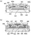
도 2a 내지 도 2d에 도시된 트랜지스터(450)는 탑-게이트 트랜지스터 중 하나인 스태거형 박막 트랜지스터이다.The
상기 트랜지스터(450)는 절연 표면을 가진 상기 기판(400) 위에 형성되는, 상기 소스 전극층(405a), 상기 드레인 전극층(405b), 상기 산화물 반도체층(403), 산화물 절연층(437), 보호 절연층(438), 및 상기 게이트 전극층(401)을 포함한다. 상기 산화물 절연층(437) 및 상기 보호 절연층(438)은 게이트 절연층으로서 작용한다.The
도 2a 내지 도 2d는 상기 트랜지스터(450)를 제작하기 위한 방법의 일 예를 도시한다.2A to 2D illustrate an example of a method for fabricating the
먼저, 절연층(436)이 절연 표면을 가진 상기 기판(400) 위에 형성된다.First, an insulating
상기 소스 전극층(405a) 및 상기 드레인 전극층(405b)은 상기 절연층(436) 위에 형성된다. 산화물 반도체층(451)은 상기 산화물 반도체층(441)의 것과 유사한 방식으로, 상기 절연층(436), 상기 소스 전극층(405a), 및 상기 드레인 전극층(405b) 위에 형성된다. 이 실시예에서, 산화물 반도체 막이 스퍼터링법에 의해 In-Ga-Zn-O계 금속 산화물 타겟을 사용하여 형성되며, In-Ga-Zn-O계 산화물 반도체 막은 섬형상 산화물 반도체층(451)으로 처리된다(도 2a 참조).The
게이트 절연층으로서 기능하는 상기 산화물 절연층(437)은 상기 산화물 반도체층(451) 위에 형성된다. 상기 산화물 절연층(437)은 상기 산화물 절연층(407)의 것과 유사한 방식으로 형성된다. 이 실시예에서, 산화 실리콘막은 스퍼터링법에 의해 상기 산화물 절연층(437)으로서 200 nm의 두께를 갖도록 형성된다.The
다음으로, 상기 산소(421)가 상기 산화물 절연층(437)을 통해 상기 산화물 반도체층(451)으로 도입된다(도 2b 참조). 상기 산소(421)를 도입하기 위한 방법으로서, 이온 주입법, 이온 도핑법 등이 사용될 수 있다. 이 실시예에서, 이온 주입법이 산소를 도입하기 위해 산소 가스를 사용하여 수행된다.Next, the
산소가 상기 산화물 반도체층(451) 위에 적층된 상기 산화물 절연층(437)을 통해 상기 산화물 반도체층(451)에 도입되며, 따라서 산소가 도입되는 도입 깊이(도입 영역)가 제어될 수 있고 따라서 산소가 상기 산화물 반도체층(451)에 충분히 도입될 수 있다. 산소가 도입되는 상기 깊이는 가속 전압 및 도즈량과 같은 도입 조건 또는 상기 산소가 통과하는 산화물 절연층(437)의 두께를 적절히 설정함으로써 제어될 수 있다. 예를 들면, 산소 가스가 사용되고 산소가 이온 주입법에 의해 도입되는 경우에, 상기 도즈량은 1×10¹³ 이온/㎠ 이상 5×10¹⁵ 이온/㎠ 이하의 범위에서 설정될 수 있다.Oxygen is introduced into the
특히, 산화물 반도체층의 채널 형성 영역에 수소, 물, 수산기, 또는 수소화물과 같은 불순물들을 제거하는 것이 중요하며, 따라서 탑-게이트 구조를 가진 상기 트랜지스터(450)에서, 많은 양의 산소가 바람직하게는 상기 산화물 반도체층(451)에서 상기 산화물 절연층(437)과의 계면의 부근에 도입된다.Particularly, it is important to remove impurities such as hydrogen, water, hydroxyl, or hydride in the channel forming region of the oxide semiconductor layer, and therefore, in the
상기 산화물 반도체층에서 상기 도입된 산소 농도의 피크는 1×10¹⁸ /㎤ 내지 3×10²⁰ /㎤(보다 바람직하게는, 1×10¹⁸ /㎤ 내지 1×10²⁰ /㎤)인 것이 바람직하다.The peak of the introduced oxygen concentration in the oxide semiconductor layer is preferably 1 × 10¹⁸ / cm 3 to 3 × 10²⁰ / cm 3 (more preferably 1 × 10¹⁸ / cm 3 to 1 × 10²⁰ / cm 3) .
상술된 산소 농도는 다음 방식으로 측정될 수 있다: 질량수 18의 산소 동위원소가 산소로서 도입되며, 상기 도입 후, 상기 산화물 반도체층에서의 상기 질량 수 18의 산소 동위 원소의 농도는 2차 이온 질량 분석법(SIMS)에 의해 분석된다.The oxygen concentration described above can be measured in the following manner: the oxygen isotope of mass number 18 is introduced as oxygen, and after the introduction, the concentration of the oxygen isotope of the mass number 18 in the oxide semiconductor layer is the secondary ion mass Analysis (SIMS).
다음으로, 산소가 도입되고 상기 산화물 절연층(437)과 접하는 상기 산화물 반도체층(451)이 열 처리된다.Next, the
상기 열 처리의 온도는 250℃ 이상 700℃ 이하, 바람직하게는 400℃ 이상 700℃ 이하, 또는 상기 기판의 변형점 미만이다. 상기 열 처리는 질소, 산소, 초-건조 공기(물 함유량이 20 ppm 이하, 바람직하게는 1 ppm 이하, 보다 바람직하게는 10 ppb 이하인 공기), 또는 희가스(아르곤, 헬륨 등)의 분위기 하에서 수행될 수 있다. 물, 수소 등이 질소, 산소, 초-건조 공기, 또는 희가스의 분위기에 포함되지 않는 것이 바람직하다는 것을 주의하자. 예를 들면, 상기 기판이 열 처리 장치의 한 종류인 전기로에 넣어진 후, 상기 산화물 반도체층(451)은 질소 분위기에서 450℃에서 1시간 동안 열 처리된다.The temperature of the heat treatment is not less than 250 ° C and not more than 700 ° C, preferably not less than 400 ° C and not more than 700 ° C, or less than the strain point of the substrate. The heat treatment may be carried out in an atmosphere of nitrogen, oxygen, super-dry air (water having a water content of 20 ppm or less, preferably 1 ppm or less, more preferably 10 ppb or less) or rare gas (argon, helium, etc.) . It is preferable that water, hydrogen, and the like are not included in the atmosphere of nitrogen, oxygen, super-dry air, or rare gas. For example, after the substrate is put in an electric furnace which is a kind of a heat treatment apparatus, the
상기 산소의 도입에 의해, 상기 산화물 반도체에 포함된 금속 및 수소 사이의 결합 또는 상기 금속 및 수산기 사이의 결합이 절단된다. 동시에, 상기 수소 또는 상기 수산기는 물을 생성하기 위해 산소와 반응한다. 결과적으로, 불순물인 수소 또는 수산기는 나중에 수행된 열 처리에 의해 물로서 쉽게 제거될 수 있다.By the introduction of the oxygen, the bond between the metal and hydrogen contained in the oxide semiconductor or the bond between the metal and the hydroxyl group is cleaved. At the same time, the hydrogen or the hydroxyl reacts with oxygen to produce water. As a result, impurities such as hydrogen or hydroxyl groups can be easily removed as water by a later heat treatment.
상기 산소의 도입 및 상기 열 처리에 의해, 상기 산화물 반도체층(451)은 탈수화 또는 탈수소화될 수 있으며, 그에 의해 수소, 물, 수산기, 또는 수소화물과 같은 불순물들이 상기 산화물 반도체층으로부터 제거될 수 있다.By the introduction of oxygen and the heat treatment, the
상기 산화물 반도체층(451) 및 산소를 포함한 상기 산화물 절연층(437)은 열 처리될 때 서로 접하며; 따라서, 상기 산화물 반도체층의 주성분 중 하나이고 불순물들을 제거하는 단계에서 감소되는 산소가, 산소를 포함한 상기 산화물 절연층(437)으로부터 상기 산화물 반도체층(451)으로 공급될 수 있다. 상기 공정을 통해, 상기 산화물 반도체층(451)은 고정제되며, 따라서 상기 전기적으로 i-형(진성) 산화물 반도체층(403)이 획득된다(도 2c 참조).The
수분 또는 수소와 같은 불순물들이 외부로부터 들어오는 것을 방지하는 상기 보호 절연층(438)이 바람직하게는 이들 불순물들이 상기 산화물 반도체층(403)에 다시 포함되지 않도록 상기 산화물 절연층(437) 위에 형성된다. 상기 보호 절연층(438)은 또한 상기 산화물 절연층(437)과 같이 게이트 절연층으로서 기능한다. 예를 들면, 질화 실리콘막이 RF 스퍼터링법에 의해 상기 보호 절연층(438)으로서 형성된다.The protective
상기 게이트 전극층(401)이 상기 산화물 반도체층(403)과 중첩하는 상기 보호 절연층(438) 위에 형성된다.The
상기 공정을 통해, 상기 트랜지스터(450)가 형성된다(도 2d 참조). 상기 트랜지스터(450)는 고정제되고 그로부터 수소, 수분, 수산기, 또는 수소화물(또한 수소 화합물이라 불림)과 같은 불순물들이 의도적으로 제거되는 상기 산화물 반도체층(403)을 포함한 트랜지스터이다. 그러므로, 상기 트랜지스터(450)의 전기적 특성들에서의 변화가 억제되며 상기 트랜지스터(450)는 전기적으로 안정된다.Through the above process, the
상술된 바와 같이, 안정된 전기적 특성들을 가진 산화물 반도체를 포함한 반도체 장치가 제공될 수 있다. 그러므로, 높은 신뢰성을 가진 반도체 장치가 제공될 수 있다.As described above, a semiconductor device including an oxide semiconductor having stable electrical characteristics can be provided. Therefore, a semiconductor device with high reliability can be provided.
이 실시예는 또 다른 실시예와 적절하게 조합하여 실시될 수 있다.This embodiment can be implemented in appropriate combination with another embodiment.
(실시예 3)(Example 3)
이 실시예에서, 반도체 장치 및 상기 반도체 장치를 제작하기 위한 방법의 또 다른 실시예가 도 3a 내지 도 3e를 참조하여 설명될 것이다. 상기 실시예에서의 것들과 동일한 부분 또는 그것과 유사한 기능을 가진 부분은 상기 실시예에 설명된 것과 유사한 방식으로 형성될 수 있고, 또한 상기 실시예에서의 것들과 유사한 단계들이 상기 실시예에서 설명된 것과 유사한 방식으로 수행될 수 있으며, 반복적인 설명은 생략된다. 또한, 동일한 부분들에 대한 상세한 설명은 생략된다.In this embodiment, another embodiment of a semiconductor device and a method for manufacturing the semiconductor device will be described with reference to Figs. 3A to 3E. Parts having the same or similar functions as those in the above embodiment can be formed in a manner similar to that described in the above embodiment, and steps similar to those in the above embodiment can be formed in the same manner as that described in the above embodiment And the repetitive description is omitted. Further, detailed description of the same parts is omitted.
도 3a 내지 도 3e에 도시된 트랜지스터(420)는 채널-보호 트랜지스터들(또한 채널-정지 트랜지스터들이라 불림)로서 불리우는 보텀-게이트 트랜지스터들 중 하나이며, 또한 역 스태거형 박막 트랜지스터라 불리운다.The
상기 트랜지스터(420)는 절연 표면을 가진 상기 기판(400) 위에 형성되는, 상기 게이트 전극층(401), 상기 게이트 절연층(402), 상기 산화물 반도체층(403), 상기 산화물 반도체층(403)의 채널 형성 영역을 커버하기 위한 채널 보호 층으로서 기능하는 산화물 절연층(427), 및 상기 소스 전극층(405a), 및 상기 드레인 전극층(405b)을 포함한다. 또한, 채널 절연층(409)은 상기 트랜지스터(420)를 커버하도록 형성된다.The
도 3a 내지 도 3e는 트랜지스터(420)를 제작하기 위한 방법의 일 예를 도시한다.Figures 3A-3E illustrate an example of a method for fabricating
먼저, 상기 게이트 전극(401)은 절연 표면을 가진 상기 기판(400) 위에 형성된다. 상기 게이트 절연층(402)은 상기 게이트 전극층(401) 위에 형성된다.First, the
다음으로, 산화물 반도체층(422)은 상기 산화물 반도체층(441)의 것과 유사한 방식으로 상기 게이트 절연층(402) 위에 형성된다. 이 실시예에서, In-Ga-Zn-O계 산화물 막이 스퍼터링법에 의해 In-Ga-Zn-O계 금속 산화물 타겟을 사용하여 형성되며, 상기 In-Ga-Zn-O계 산화물 막은 상기 섬형상 산화물 반도체층(422)으로 처리된다.Next, an
산화물 절연층(426)은 상기 산화물 절연층(407)과 같이 상기 산화물 반도체층(422) 위에 형성된다(도 3a 참조). 이 실시예에서, 산화 실리콘막은 스퍼터링법에 의해 상기 산화물 절연층(426)으로서 200 nm의 두께를 갖도록 형성된다.The
다음으로, 상기 산소(421)가 상기 산화물 절연층(426)을 통해 상기 산화물 반도체층(422)으로 도입된다(도 3b 참조). 상기 산소(421)를 도입하기 위한 방법으로서, 이온 주입법, 이온 도핑법 등이 사용될 수 있다. 이 실시예에서, 이온 주입법이 산소를 도입하기 위해 산소를 사용하여 수행된다.Next, the
산소가 상기 산화물 반도체층(422) 위에 적층된 상기 산화물 절연층(426)을 통해 상기 산화물 반도체층(422)에 도입되며, 따라서 산소가 도입되는 도입 깊이(도입 영역)는 제어될 수 있고 따라서 산소가 상기 산화물 반도체층(422)에 충분히 도입될 수 있다. 산소가 도입되는 상기 깊이는 가속 전압 및 도즈량과 같은 도입 조건 또는 상기 산소가 통과하는 산화물 절연층(426)의 두께를 적절히 설정함으로써 제어될 수 있다. 예를 들면, 산소 가스가 사용되고 산소가 이온 주입법에 의해 도입되는 경우에, 상기 도즈량은 1×10¹³ 이온/㎠ 내지 5×10¹⁵ 이온/㎠의 범위에서 설정될 수 있다.Oxygen is introduced into the
특히, 산화물 반도체층(422)의 채널 형성 영역에 수소, 물, 수산기, 또는 수소화물과 같은 불순물들을 제거하는 것이 중요하며, 따라서 보텀-게이트 구조를 가진 상기 트랜지스터(420)에서, 많은 양의 산소가 바람직하게는 상기 산화물 반도체층(422)에서 상기 게이트 절연층(402)과의 계면의 부근에 도입된다.Particularly, it is important to remove impurities such as hydrogen, water, hydroxyl, or hydride in the channel forming region of the
상기 산화물 반도체층(422)에서 상기 도입된 산소 농도의 피크는 1×10¹⁸ /㎤ 내지 3×10²⁰ /㎤(보다 바람직하게는, 1×10¹⁸ /㎤ 내지 1×10²⁰ /㎤)인 것이 바람직하다.The peak of the introduced oxygen concentration in the
상술된 산소 농도는 다음 방식으로 측정될 수 있다: 질량수 18의 산소 동위원소가 산소로서 도입되며, 상기 도입 후, 상기 산화물 반도체층에서의 상기 질량 수 18의 산소 동위원소의 농도는 2차 이온 질량 분석법(SIMS)에 의해 분석된다.The oxygen concentration described above can be measured in the following manner: the oxygen isotope of mass number 18 is introduced as oxygen, and after the introduction, the concentration of the oxygen isotope of the mass number 18 in the oxide semiconductor layer is the secondary ion mass Analysis (SIMS).
다음으로, 산소가 도입되고 상기 산화물 절연층(426)과 접하는 상기 산화물 반도체층(422)이 열 처리된다.Next, the
상기 열 처리의 온도는 250℃ 내지 700℃, 바람직하게는 400℃ 내지 700℃, 또는 상기 기판의 변형점 미만이다. 상기 열 처리는 질소, 산소, 초-건조 대기(물 함유량이 20 ppm 이하, 바람직하게는 1 ppm 이하, 보다 바람직하게는 10 ppb 이하인 공기), 또는 희가스(아르곤, 헬륨 등)의 분위기 하에서 수행될 수 있다. 물, 수소 등이 질소, 산소, 초-건조 공기, 또는 희가스의 분위기에 포함되지 않는 것이 바람직하다는 것을 주의하자. 예를 들면, 상기 기판이 열 처리 장치의 한 종류인 전기로에 넣어진 후, 상기 산화물 반도체층(422)은 질소 분위기에서 1시간 동안 450℃에서 열 처리된다.The temperature of the heat treatment is 250 ° C to 700 ° C, preferably 400 ° C to 700 ° C, or less than the strain point of the substrate. The heat treatment may be performed in an atmosphere of nitrogen, oxygen, a super-drying atmosphere (water having a water content of 20 ppm or less, preferably 1 ppm or less, more preferably 10 ppb or less), or rare gas (argon, helium, etc.) . It is preferable that water, hydrogen, and the like are not included in the atmosphere of nitrogen, oxygen, super-dry air, or rare gas. For example, after the substrate is put in an electric furnace which is one kind of heat treatment apparatus, the
상기 산소의 도입에 의해, 상기 산화물 반도체에 포함된 금속 및 수소 사이의 결합 또는 상기 금속 및 수산기 사이의 결합이 절단된다. 동시에, 상기 수소 또는 상기 수산기는 물을 생성하기 위해 산소와 반응한다. 결과적으로, 불순물인 수소 또는 수산기는 나중에 수행된 상기 열 처리에 의해 물로서 쉽게 제거될 수 있다.By the introduction of the oxygen, the bond between the metal and hydrogen contained in the oxide semiconductor or the bond between the metal and the hydroxyl group is cleaved. At the same time, the hydrogen or the hydroxyl reacts with oxygen to produce water. As a result, impurities such as hydrogen or hydroxyl groups can be easily removed as water by the heat treatment performed later.
상기 산소의 도입 및 상기 열 처리에 의해, 상기 산화물 반도체층(422)은 탈수화 또는 탈수소화될 수 있으며, 그에 의해 수소, 물, 수산기, 또는 수소화물과 같은 불순물들이 상기 산화물 반도체층(422)으로부터 제거될 수 있다.The
상기 산화물 반도체층(422) 및 산소를 포함한 상기 산화물 절연층(426)은 열 처리될 때 서로 접하며; 따라서, 상기 산화물 반도체층의 주성분 중 하나이고 불순물들을 제거하는 단계에서 감소되는 산소가 산소를 포함한 상기 산화물 절연층(426)으로부터 상기 산화물 반도체층(422)으로 공급될 수 있다. 상기 공정을 통해, 상기 산화물 반도체층(422)은 고정제되며, 따라서 상기 전기적으로 i-형(진성) 산화물 반도체층(403)이 획득된다.The
상기 산화물 절연층(426)은 포토리소그래피 단계에 의해 상기 산화물 반도체층(403)의 상기 채널 형성 영역을 커버하는 채널 보호층으로서 기능하는 상기 산화물 절연층(427)으로 처리된다(도 3d 참조). 상기 산화물 절연층(426)을 에칭하기 위한 이 단계 동안, 상기 산화물 반도체층(403)의 일부가 몇몇 경우들에서 제거된다는 것을 주의하자. 이 경우에, 상기 산화물 절연층(427)으로 커버되지 않는 상기 산화물 반도체층(403)의 영역의 두께는 작아진다.The
상기 소스 전극층(405a) 및 상기 드레인 전극층(405b)은 상기 산화물 반도체층(403) 및 상기 산화물 절연층(427) 위에 형성된다.The
상기 공정을 통해, 상기 트랜지스터(420)가 형성된다(도 3e 참조). 상기 트랜지스터(420)는 고정제되고 그로부터 수소, 수분, 수산기, 또는 수소화물(또한 수소 화합물이라 불림)과 같은 불순물들이 의도적으로 제거되는 상기 산화물 반도체층(403)을 포함한 트랜지스터이다. 그러므로, 상기 트랜지스터(420)의 전기적 특성들에서의 변화가 억제되며 상기 트랜지스터(420)는 전기적으로 안정된다.Through the above process, the
수분 또는 수소와 같은 불순물들이 외부로부터 들어가는 것을 방지하는 상기 보호 절연층(409)이 이들 불순물들이 다시 상기 산화물 반도체층(403)에 포함되지 않도록 상기 산화물 반도체층(427), 상기 소스 전극층(405a), 및 상기 드레인 전극층(405b) 위에 형성된다(도 3e 참조). 예를 들면, 질화 실리콘막이 RF 스퍼터링법에 의해 상기 보호 절연층(409)으로서 형성된다.The protective
상술된 바와 같이, 안정된 전기적 특성들을 가진 산화물 반도체를 포함한 반도체 장치가 제공될 수 있다. 그러므로, 높은 신뢰성을 가진 반도체 장치가 제공될 수 있다.As described above, a semiconductor device including an oxide semiconductor having stable electrical characteristics can be provided. Therefore, a semiconductor device with high reliability can be provided.
이 실시예는 또 다른 실시예와 적절하게 조합하여 실시될 수 있다.This embodiment can be implemented in appropriate combination with another embodiment.
(실시예 4)(Example 4)
이 실시예에서, 반도체 장치 및 상기 반도체 장치를 제작하기 위한 방법의 또 다른 실시예가 도 4a 및 도 4b를 참조하여 설명될 것이다. 이 실시예에서, 트랜지스터는 상기 반도체 장치의 일 예로서 도시될 것이다. 상기 실시예에서의 것들과 동일한 부분 또는 그것과 유사한 기능을 가진 부분은 상기 실시예에 설명된 것과 유사한 방식으로 형성될 수 있고, 또한 상기 실시예에서의 것들과 유사한 단계들이 상기 실시예에서 설명된 것과 유사한 방식으로 수행될 수 있으며, 반복적인 설명은 생략된다. 또한, 동일한 부분들에 대한 상세한 설명은 생략된다.In this embodiment, another embodiment of a semiconductor device and a method for manufacturing the semiconductor device will be described with reference to Figs. 4A and 4B. In this embodiment, the transistor will be shown as an example of the semiconductor device. Parts having the same or similar functions as those in the above embodiment can be formed in a manner similar to that described in the above embodiment, and steps similar to those in the above embodiment can be formed in the same manner as that described in the above embodiment And the repetitive description is omitted. Further, detailed description of the same parts is omitted.
상기 트랜지스터의 구조에 대한 특별한 제한은 없으며; 예를 들면, 스태거형 트랜지스터 또는 탑-게이트 구조 또는 보텀-게이트 구조를 가진 평면형 트랜지스터가 이용될 수 있다. 또한, 상기 트랜지스터는 하나의 채널 형성 영역을 포함한 단일 게이트 구조, 두 개의 채널 형성 영역들을 포함한 이중 게이트 구조, 또는 3개의 채널 형성 영역들을 포함한 3중 게이트 구조를 가질 수 있다. 더욱이, 상기 트랜지스터는 게이트 절연층을 사이에 제공하여 채널 영역 위 및 아래에 위치된 두 개의 게이트 전극층들을 포함한 이중 게이트 구조를 가질 수 있다.There is no particular limitation on the structure of the transistor; For example, a staggered transistor or a planar transistor having a top-gate structure or a bottom-gate structure may be used. In addition, the transistor may have a single gate structure including one channel formation region, a double gate structure including two channel formation regions, or a triple gate structure including three channel formation regions. Furthermore, the transistor may have a double gate structure including two gate electrode layers located above and below the channel region by providing a gate insulating layer therebetween.
도 4a 및 도 4b에 도시된 상기 트랜지스터의 단면 구조의 예들이 이하에 설명될 것임을 주의하자. 도 4a 및 도 4b에 도시된 트랜지스터들(430, 440)은 실시예 1 내지 실시예 3에 도시된 상기 트랜지스터들(410, 420, 450)과 같은 트랜지스터들이며; 상기 트랜지스터들(430, 440)은 고정제되고 그로부터 수소, 수분, 수산기, 또는 수소화물(또한 수소 화합물이라 불림)과 같은 불순물들이 의도적으로 제거되는 상기 산화물 반도체층을 포함한다. 그러므로, 상기 트랜지스터들(430, 440)의 전기적 특성들에서의 변화가 억제되고 상기 트랜지스터(430, 440)는 전기적으로 안정된다. 결과적으로, 높은 신뢰성을 가진 반도체 장치가 제공될 수 있다.Note that examples of the cross-sectional structures of the transistors shown in Figs. 4A and 4B will be described below. The
도 4a에 도시된 상기 트랜지스터(430)는 보텀-게이트 트랜지스터이다. 상기 트랜지스터(430)는 절연 표면을 가진 상기 기판(400) 위에 형성되는, 상기 게이트 전극층(401), 상기 게이트 절연층(402), 상기 소스 전극층(405a), 상기 드레인 전극층(405b), 및 상기 산화물 반도체층(403)을 포함한다. 상기 산화물 절연층(407)은 상기 트랜지스터(430)를 커버하기 위해 제공되며 상기 산화물 반도체층(403)과 접한다. 또한, 상기 보호 절연층(409)은 상기 산화물 절연층(407) 위에 형성된다.The
상기 트랜지스터(430)에서, 상기 게이트 절연층(402)은 상기 기판(400) 및 상기 게이트 전극층(401) 위에 제공되며 그것과 접한다. 상기 소스 전극층(405a) 및 상기 드레인 전극층(405b)은 상기 게이트 절연층(402) 위에 제공되며 그것과 접한다. 상기 산화물 반도체층(403)은 상기 게이트 절연층(402), 상기 소스 전극층(405a), 및 상기 드레인 전극층(405b) 위에 제공된다.In the
도 4b에 도시된 상기 트랜지스터(440)는 탑-게이트 트랜지스터이다. 상기 트랜지스터(440)는 절연 표면을 가진 상기 기판(400) 위에 형성되는, 상기 절연층(436), 상기 산화물 반도체층(403), 상기 소스 전극층(405a), 상기 드레인 전극층(405b), 게이트 절연층을 형성하는 산화물 절연층(467) 및 보호 절연층(468), 및 상기 게이트 전극층(401)을 포함한다. 배선층(465a) 및 배선층(465b)이 각각 상기 소스 전극층(405a) 및 상기 드레인 전극층(405b)과 접하도록 제공되고 그것에 전기적으로 접속된다. 보호 절연층(469)은 상기 게이트 전극층(401), 상기 배선층(465a), 및 상기 배선층(465b)을 커버하도록 형성된다.The
상기 산화물 반도체층(403)을 위해 사용된 산화물 반도체로서, In-Sn-Ga-Zn-O계 산화물 반도체와 같은 4-원계 금속 산화물; In-Ga-Zn-O계 산화물 반도체, In-Sn-Zn-O계 산화물 반도체, In-Al-Zn-O계 산화물 반도체, Sn-Ga-Zn-O계 산화물 반도체, Al-Ga-Zn-O계 산화물 반도체, 또는 Sn-Al-Zn-O계 산화물 반도체와 같은 3-원계 금속 산화물; In-Zn-O계 산화물 반도체, Sn-Zn-O계 산화물 반도체, Al-Zn-O계 산화물 반도체, Zn-Mg-O계 산화물 반도체, Sn-Mg-O계 산화물 반도체, 또는 In-Mg-O계 산화물 반도체와 같은 2-원계 금속 산화물; In-O계 산화물 반도체; Sn-O계 산화물 반도체; 또는 Zn-O계 산화물 반도체가 사용될 수 있다. 또한, SiO2가 상기 산화물 반도체에 포함될 수 있다. 여기에서, 예를 들면, In-Ga-Zn-O계 산화물 반도체는 적어도 In, Ga, 및 Zn을 포함한 산화물이며, 그 조성비에 대한 특별한 제한은 없다. 더욱이, In-Ga-Zn-O계 산화물 반도체는 In, Ga, 및 Zn 이외의 다른 원소를 포함할 수 있다.As the oxide semiconductor used for the
상기 산화물 반도체층(403)을 위해, InMO3(ZnO)m(m>0, 및 m은 자연수가 아니다)에 의해 표현된 박막이 사용될 수 있다.여기에서, M은 Ga, Al, Mn, 및 Co로부터 선택된 하나 이상의 금속 원소들을 나타낸다. 예를 들면, M은 Ga, Ga와 Al, Ga와 Mn, Ga와 Co 등일 수 있다.For the
상기 보텀-게이트 트랜지스터(430)에서, 하지 막으로서 작용하는 절연막이 상기 기판 및 상기 게이트 전극층 사이에 제공될 수 있다. 상기 하지 막은 상기 기판으로부터 불순물 원소의 확산을 방지하는 기능을 가지며, 질화 실리콘막, 산화 실리콘막, 질화 산화 실리콘막, 및 산질화 실리콘막 중 하나 이상을 사용한 단층 구조 또는 적층 구조를 갖도록 형성될 수 있다.In the
상기 기판(400), 상기 게이트 전극층(401), 상기 게이트 절연층(402), 상기 소스 전극층(405a), 및 상기 드레인 전극층(405b)는 실시예 1에서의 것들과 유사한 재료 및 방법을 사용하여 형성될 수 있다.The
상기 소스 전극층(405a) 및 상기 드레인 전극층(405b)의 것과 유사한 재료가 각각 상기 소스 전극층(405a) 및 상기 드레인 전극층(405b)에 접속되는 상기 배선층(465a) 및 상기 배선층(465b)과 같은 도전막들을 위해 사용될 수 있다.Materials similar to those of the
상기 절연층(436) 및 게이트 절연층으로서 기능하는 상기 산화물 절연층(467)이 상기 산화물 절연층(407)의 것과 유사한 재료를 사용하여 형성될 수 있다. 통상적으로, 산화 실리콘막 또는 산질화 실리콘막과 같은 무기 절연막이 사용될 수 있다.The insulating
게이트 절연층으로서 기능하는 상기 보호 절연층(468) 및 상기 보호 절연층(469)을 위해, 질화 실리콘막, 질화 알루미늄 막, 질화 산화 실리콘막, 질화 산화 알루미늄 막, 또는 산화 알루미늄 막과 같은 무기 절연막이 사용될 수 있다.An inorganic insulating film such as a silicon nitride film, an aluminum nitride film, a silicon nitride oxide film, an aluminum nitride oxide film, or an aluminum oxide film for the protective insulating
또한, 평탄화 절연막이 상기 트랜지스터로 인한 표면 거칠기가 감소되도록 상기 보호 절연층(409) 위에 형성될 수 있다. 상기 평탄화 절연막을 위해, 폴리이미드, 아크릴, 또는 벤조사이클로부텐과 같은 유기 재료가 사용될 수 있다. 이러한 유기 재료들 이외에, 저-유전율 재료(로우-k(low-k) 재료) 등을 사용하는 것이 또한 가능하다. 상기 평탄화 절연막은 이들 재료들로부터 형성된 복수의 절연막들을 적층함으로써 형성될 수 있다는 것을 주의하자.In addition, a planarization insulating film may be formed on the protective insulating
상기 트랜지스터들(430, 440)에서, 상기 산화물 반도체층(403)은 고정제되고 그로부터 수소, 수분, 수산기, 또는 수소화물(또한 수소 화합물이라 불림)과 같은 불순물들이 상기 산화물 반도체층(403) 위에 적층된 상기 산화물 절연층들(407, 467)을 통해 산소를 도입하고 열 처리를 수행함으로써 의도적으로 제거되는 산화물 반도체층이다. 산소를 도입함으로써, 상기 산화물 반도체에 포함된 금속 및 수소 사이의 결합 또는 상기 금속 및 수산기 사이의 결합이 절단되며, 상기 수소 또는 상기 수산기는 물을 생성하기 위해 산소와 반응하고, 이는 나중에 수행된 열 처리에 의해 물로서, 불순물인 수소 또는 수산기의 용이한 제거를 이끈다.In the
산소는 상기 산화물 반도체층 위에 적층된 산화물 절연층을 통해 상기 산화물 반도체층에 도입되며, 따라서 산소가 도입되는 도입 깊이(도입 영역)가 제어될 수 있고 따라서 산소는 상기 산화물 반도체층에 효율적으로 도입될 수 있다.Oxygen is introduced into the oxide semiconductor layer through the oxide insulating layer stacked on the oxide semiconductor layer, so that the introduction depth (introduction region) through which oxygen is introduced can be controlled so that oxygen is efficiently introduced into the oxide semiconductor layer .
산소를 포함한 상기 산화물 절연층들(407, 467)의 각각은 상기 열처리가 될 때 상기 산화물 반도체층과 접하며; 따라서 상기 산화물 반도체의 주성분 중 하나이고 불순물들을 제거하는 단계에서 감소되는 산소가 산소를 포함한 상기 산화물 절연층들(407, 467)의 각각으로부터 상기 산화물 반도체층으로 공급될 수 있다. 따라서, 상기 산화물 반도체층(403)은 전기적으로 i-형(진성)이 되도록 보다 고정제된다.Each of the
상기 고정제된 산화물 반도체층(403)을 포함한 상기 트랜지스터들(430, 440)의 각각에서, 오프 상태에서의 전류(오프-상태 전류)는 작을 수 있다.In each of the
각각 상기 고정제된 산화물 반도체층(403)을 포함한 상기 트랜지스터들(430, 440)의 전계-효과 이동도는 비교적 높을 수 있으며, 그에 의해 고속 동작이 가능하다. 예를 들면, 고속으로 동작할 수 있는 이러한 트랜지스터가 액정 표시 장치를 위해 사용될 때, 화소부에서의 스위칭 트랜지스터 및 구동 회로부에서의 구동기 트랜지스터가 하나의 기판 위에 형성될 수 있다. 즉, 실리콘 웨이퍼 등으로 형성된 반도체 장치가 부가적으로 구동 회로로서 요구되지 않기 때문에, 상기 반도체 장치의 구성요소들의 수는 감소될 수 있다. 또한, 화소부에서 고속으로 동작할 수 있는 트랜지스터를 사용함으로써, 고-품질 이미지가 제공될 수 있다.The field-effect mobility of the
상술된 바와 같이, 안정된 전기적 특성들을 가진 산화물 반도체를 포함한 반도체 장치가 제공될 수 있다. 결과적으로, 높은 신뢰성을 가진 반도체 장치가 제공될 수 있다.As described above, a semiconductor device including an oxide semiconductor having stable electrical characteristics can be provided. As a result, a semiconductor device with high reliability can be provided.
(실시예 5)(Example 5)
이 실시예에서, 반도체 장치의 또 다른 실시예가 도 1a 내지 도 1e 및 도 5a 내지 도 5d를 참조하여 설명된다. 상기 실시예에서의 것들과 동일한 부분 또는 그것과 유사한 기능을 가진 부분은 상기 실시예에 설명된 것과 유사한 방식으로 형성될 수 있고, 또한 상기 실시예에서의 것들과 유사한 단계들이 상기 실시예에서 설명된 것과 유사한 방식으로 수행될 수 있으며, 반복적인 설명은 생략된다. 또한, 동일한 부분들에 대한 상세한 설명은 생략된다.In this embodiment, another embodiment of the semiconductor device is described with reference to Figs. 1A to 1E and 5A to 5D. Parts having the same or similar functions as those in the above embodiment can be formed in a manner similar to that described in the above embodiment, and steps similar to those in the above embodiment can be formed in the same manner as that described in the above embodiment And the repetitive description is omitted. Further, detailed description of the same parts is omitted.
이 실시예에서, 트랜지스터의 소스 전극층 및/또는 드레인 전극층이 도전층(예컨대, 배선층 또는 화소 전극층)에 연결되는 구조의 일 예가 도시된다. 이 실시예에서, 실시예 1에 도시된 상기 트랜지스터(410)는 설명에서의 하나의 트랜지스터로서 사용되지만, 실시예 2 내지 실시예 4에 도시된 임의의 다른 트랜지스터들이 사용될 수 있다는 것을 주의하자.In this embodiment, an example of a structure in which a source electrode layer and / or a drain electrode layer of a transistor is connected to a conductive layer (for example, a wiring layer or a pixel electrode layer) is shown. Note that in this embodiment, the
도 5a에 도시된 바와 같이, 상기 트랜지스터(410)는 절연 표면을 가진 상기 기판(400) 위에 형성되는 상기 게이트 전극층(401), 상기 게이트 절연층(402), 상기 산화물 반도체층(403), 상기 소스 전극층(405a), 및 상기 드레인 전극층(405b)을 포함한다. 상기 산화물 절연층(407) 및 상기 보호 절연층(409)은 이러한 순서로 상기 트랜지스터(410) 위에 적층된다.5A, the
실시예 1에 도시된 바와 같이, 상기 트랜지스터(410)의 제작 공정에서, 상기 산화물 절연층(407)이 상기 산화물 반도체층(403), 상기 소스 전극층(405a), 및 상기 드레인 전극층(405b) 위에 형성되며, 상기 산소(421)는 상기 산화물 절연층(407)을 통해 상기 산화물 반도체층(441)에 도입되고 열 처리가 수행된다(도 1b 내지 도 1d 참조). 이러한 산소 도입 및 열 처리 단계 동안, 상기 산소(421)는 상기 산화물 반도체층(403) 외에도 상기 소스 전극층(405a) 및 상기 드레인 전극층(405b)에 도달하고 그것에 조사된다(표면의 부근에 도입된다). 따라서, 도 5a에 도시된 바와 같이, 상기 산소(421)로 조사된 상기 소스 전극층(405a) 및 상기 드레인 전극층(405b)의 표면은 산화되며, 금속 산화물 영역들(404a, 404b)은 몇몇 경우들에서 각각 상기 소스 전극층(405a)과 상기 산화물 절연층(407) 사이 및 상기 드레인 전극층(405b)과 상기 산화물 절연층(407) 사이에 형성된다. 상기 금속 산화물 영역들(404a, 404b)은 몇몇 경우들에서 막의 형태로 있을 수 있다.The
도 5a의 경우에서, 상기 소스 전극층(405a) 및 상기 드레인 전극층(405b)에 연결된 상기 도전층을 형성하기 위한 개구들(455a, 455b)이 바람직하게는 다음의 방식으로 형성된다: 높은 저항을 가진 상기 금속 산화물 영역들(404a, 404b)이 제거되며; 상기 개구들(455a, 455b)이 낮은 저항을 갖는 상기 소스 전극층(405a) 및 상기 드레인 전극층(405b)이 노출될 때까지 형성된다(도 5b 참조). 상기 보호 절연층(409), 상기 산화물 절연층(407), 및 상기 금속 산화물 영역들(404a, 404b)의 일부들이 상기 개구들(455a, 455b)을 형성하기 위해 제거된다.5A,
다음으로, 도전층들(456a, 456b)이 상기 개구들(455a, 455b)에서 노출된 상기 소스 전극층(405a) 및 상기 드레인 전극층(405b)과 접하도록 형성된다(도 5c 참조). 상기 도전층들(456a, 456b)은 높은 저항을 가진 상기 금속 산화물 영역들(404a, 404b)을 통해서가 아닌, 낮은 저항을 가진 상기 소스 전극층(405a) 및 상기 드레인 전극층(405b)과 직접 접하도록 형성되며, 따라서 양호한 전기적 연결(전기적 접촉)이 획득될 수 있다.Next,
보호 절연층(457)이 상기 트랜지스터(410)를 커버하도록 보호층으로서 상기 도전층들(456a, 456b) 위에 형성될 수 있다(도 5d 참조). 게다가, 상기 보호 절연층(457)을 커버함으로써, 수소 및 수분과 같은 불순물들이 상기 개구들(455a, 455b)로부터 상기 산화물 반도체층(403)에 들어가는 것을 방지하는 것이 가능하다.A protective insulating
상기 소스 전극층(405a) 및 상기 드레인 전극층(405b)에서, 산소가 쉽게 도입되지 않는 도전막(대표적으로, 텅스텐막, 탄탈막 등)이 산소를 갖고 조사된 상기 표면상에 형성될 수 있다. 예를 들면, 상기 소스 전극층(405a) 및 상기 드레인 전극층(405b)은 티타늄막 및 텅스텐막의 적층된 층으로 형성되며, 상기 텅스텐막은 산소가 도입되는 측 상에서 제공되고, 높은 저항을 가진 금속 산화물 영역의 형성이 억제될 수 있다.A conductive film (typically, a tungsten film, a tantalum film, or the like) in which oxygen is not readily introduced can be formed on the surface irradiated with oxygen from the
상술된 바와 같이, 트랜지스터의 양호한 전기적 연결이 획득될 수 있으며, 그에 의해 안정된 전기적 특성들을 가진 산화물 반도체를 포함한 반도체 장치가 제공될 수 있다. 그러므로, 높은 신뢰성을 가진 반도체 장치가 제공될 수 있다.As described above, a good electrical connection of the transistor can be obtained, whereby a semiconductor device including an oxide semiconductor having stable electrical characteristics can be provided. Therefore, a semiconductor device with high reliability can be provided.
(실시예 6)(Example 6)
이 실시예에서, 반도체 장치 및 상기 반도체 장치를 제작하기 위한 방법의 또 다른 실시예가 설명될 것이다. 상기 실시예에서의 것들과 동일한 부분 또는 그것과 유사한 기능을 가진 부분은 상기 실시예에 설명된 것과 유사한 방식으로 형성될 수 있고, 또한 상기 실시예에서의 것들과 유사한 단계들이 상기 실시예에서 설명된 것과 유사한 방식으로 수행될 수 있으며, 반복적인 설명은 생략된다. 또한, 동일한 부분들에 대한 상세한 설명은 생략된다.In this embodiment, another embodiment of a semiconductor device and a method for manufacturing the semiconductor device will be described. Parts having the same or similar functions as those in the above embodiment can be formed in a manner similar to that described in the above embodiment, and steps similar to those in the above embodiment can be formed in the same manner as that described in the above embodiment And the repetitive description is omitted. Further, detailed description of the same parts is omitted.
이 실시예는 실시예 1 내지 실시예 5에 도시된 상기 트랜지스터들(410, 420, 430, 440, 450) 중 임의의 것에 적용될 수 있다는 것을 주의하자.Note that this embodiment can be applied to any of the
이 실시예에서, 상기 트랜지스터들(410, 420, 430, 440, 450)을 제작하기 위한 방법에서, 상기 산화물 반도체층과 접하는 상기 산화물 절연층들(407, 437, 426, 467)을 형성하기 전에, 상기 산화물 반도체층에 열 처리를 수행하는 일 예가 도시된다.In this embodiment, in the method for fabricating the
이러한 열 처리는, 열 처리가 상기 산화물 반도체층의 형성 후 및 상기 산화물 절연층의 형성 전에 수행되는 한, 상기 산화물 반도체층이 상기 섬형상 산화물 반도체층으로 처리되기 전 상기 산화물 반도체층에서 수행될 수 있다. 상기 트랜지스터(410)의 경우에, 상기 소스 전극층(405a) 및 상기 드레인 전극층(405b)의 형성 전후에 상기 열 처리가 수행될 수 있다.This heat treatment may be performed in the oxide semiconductor layer before the oxide semiconductor layer is treated with the island-shaped oxide semiconductor layer, as long as heat treatment is performed after formation of the oxide semiconductor layer and before formation of the oxide insulating layer have. In the case of the
상기 열 처리의 온도는 400℃ 이상 750℃ 이하 또는 400℃ 이상 기판의 변형점 미만이다. 예를 들면, 상기 기판은 열 처리 장치의 한 종류인 전기로에 넣어지고, 상기 산화물 반도체층은 질소 분위기에서 1시간 동안 450℃에서 상기 열 처리가 된다. 상기 열 처리 후, 상기 산화물 절연층은 대기로의 노출 없이 형성되고 물 및 수분은 상기 산화물 반도체층에 다시 포함되는 것으로부터 방지되는 것이 바람직하다.The temperature of the heat treatment is 400 ° C or more and 750 ° C or less or 400 ° C or more and less than the strain point of the substrate. For example, the substrate is placed in an electric furnace, which is a kind of a heat treatment apparatus, and the oxide semiconductor layer is subjected to the heat treatment at 450 DEG C for 1 hour in a nitrogen atmosphere. After the thermal treatment, the oxide insulating layer is preferably formed without exposure to air, and water and moisture are prevented from being included again in the oxide semiconductor layer.
또한, 사용된 열 처리 장치는 전기로에 한정되지 않으며, 저항 발열체와 같은 발열체로부터 열 도전 또는 열 복사에 의해 피처리물을 가열하기 위한 장치가 대안적으로 사용될 수 있다. 예를 들면, 가스 급속 열 어닐(GRTA) 장치 또는 램프 급속 열 어닐(LRTA) 장치와 같은 급속 열 어닐(RTA) 장치가 사용될 수 있다. LRTA 장치는 할로겐 램프, 메탈 할라이드 램크, 크세논 아크 램프, 탄소 아크 램프, 고압 나트륨 램프, 또는 고압 수은 램프와 같은 램프로부터 방출된 광(전자기파)의 복사에 의해 피처리물을 가열하기 위한 장치이다. GRTA 장치는 고온 가스를 사용한 열 처리를 위한 장치이다. 상기 고온 가스로서, 질소 또는 희가스와 같이, 열 처리에 의해 피처리물과 반응하지 않는 불활성 가스가 사용된다.Further, the heat treatment apparatus used is not limited to the electric furnace, and an apparatus for heating the object to be processed by heat conduction or heat radiation from a heating body such as a resistance heating body may alternatively be used. For example, a rapid thermal anneal (RTA) device such as a gas rapid thermal anneal (GRTA) device or a lamp rapid thermal anneal (LRTA) device may be used. The LRTA device is a device for heating an object to be processed by radiation of light (electromagnetic waves) emitted from a lamp such as a halogen lamp, a metal halide lamp, a xenon arc lamp, a carbon arc lamp, a high pressure sodium lamp, or a high pressure mercury lamp. The GRTA device is a device for heat treatment using hot gases. As the high-temperature gas, an inert gas which does not react with the object to be treated by heat treatment such as nitrogen or a rare gas is used.
예를 들면, 상기 열 처리로서, GRTA가 다음과 같이 수행될 수 있다. 상기 기판은 650℃ 내지 700℃의 고온에서 가열된 불활성 가스에 넣어지고, 수분 동안 가열되며, 상기 불활성 가스로부터 꺼내어진다.For example, as the heat treatment, GRTA can be performed as follows. The substrate is placed in an inert gas heated at a high temperature of 650 ° C to 700 ° C, heated for a few minutes, and taken out of the inert gas.
상기 열 처리가 질소, 산소, 초-건조 공기(물 함유량이 20 ppm 이하, 바람직하게는 1 ppm 이하, 보다 바람직하게는 10 ppb 이하인 공기), 또는 희가스(아르곤, 헬륨 등)의 분위기 하에서 수행될 수 있다. 물, 수소 등이 질소, 산소, 초-건조 공기, 또는 희가스의 분위기에 포함되지 않는 것이 바람직하다는 것을 주의하자. 열 처리 장치로 도입되는 질소, 산소, 또는 희가스의 순도는 6N(99.9999%) 이상, 바람직하게는 7N(99.99999%) 이상(즉, 불순물 농도는 1 ppm 이하, 바람직하게는 0.1 ppm 이하)로 설정되는 것이 또한 바람직하다.The heat treatment may be carried out in an atmosphere of nitrogen, oxygen, super-dry air (water having a water content of 20 ppm or less, preferably 1 ppm or less, more preferably 10 ppb or less), or rare gas (argon, helium, etc.) . It is preferable that water, hydrogen, and the like are not included in the atmosphere of nitrogen, oxygen, super-dry air, or rare gas. The purity of nitrogen, oxygen, or rare gas introduced into the heat treatment apparatus is set to 6N (99.9999%) or more, preferably 7N (99.99999%) or more (i.e., the impurity concentration is 1 ppm or less, preferably 0.1 ppm or less) .
이러한 열 처리를 갖고, 상기 산화물 반도체층에서의 수분 또는 수소와 같은 불순물들이 감소될 수 있다.With such a heat treatment, impurities such as moisture or hydrogen in the oxide semiconductor layer can be reduced.
게다가, 상기 산화물 반도체층 위에 상기 산화물 절연층을 형성하고 상기 산화물 절연층을 통해 상기 산화물 반도체층에 산소를 도입함으로써, 상기 산화물 반도체에 포함된 금속 및 수소 사이의 결합 또는 상기 금속 및 수산기 사이의 결합이 절단되며, 상기 수소 또는 상기 수산기는 물을 생성하기 위해 산소와 반응한다. 그 후, 상기 열 처리는 또한 산소의 도입 후 수행되며, 그에 의해 남겨진 수소 또는 수산기와 같은 불순물들이 물로서 쉽게 제거될 수 있다.In addition, by forming the oxide insulating layer on the oxide semiconductor layer and introducing oxygen into the oxide semiconductor layer through the oxide insulating layer, a bond between the metal and hydrogen contained in the oxide semiconductor or a bond between the metal and the hydroxyl group And the hydrogen or the hydroxyl group reacts with oxygen to produce water. Thereafter, the heat treatment is also carried out after the introduction of oxygen, whereby impurities such as hydrogen or hydroxyl left behind can be easily removed as water.
상기 산화물 반도체층 및 산소를 포함한 상기 산화물 절연층은 상기 열 처리가 될 때 서로 접하며; 따라서 상기 산화물 반도체의 주성분 중 하나이고 불순물들을 제거하는 단계에서 감소되는 산소가 산소를 포함한 상기 산화물 절연층으로부터 상기 산화물 반도체층으로 공급될 수 있다.The oxide semiconductor layer and the oxide insulating layer containing oxygen are in contact with each other when the heat treatment is performed; Therefore, oxygen, which is one of the main components of the oxide semiconductor and which is reduced in the step of removing impurities, can be supplied from the oxide insulating layer containing oxygen to the oxide semiconductor layer.
따라서, 상기 산화물 반도체층이 상기 산화물 절연층을 형성하기 전에 수행된 상기 열 처리, 및 상기 산화물 절연층을 형성하고 산소 도입 후 상기 열 처리될 때, 수분 및 수소와 같은 불순물들이 제거되는 i-형(진성) 산화물 반도체 또는 실질적으로 i-형 산화물 반도체층이 획득될 수 있다.Therefore, it is preferable that the heat treatment performed before the oxide semiconductor layer is formed before forming the oxide insulating layer and the i-type oxide semiconductor layer in which impurities such as moisture and hydrogen are removed when the oxide insulating layer is formed and the heat treatment is performed after oxygen introduction (Intrinsic) oxide semiconductor or a substantially i-type oxide semiconductor layer can be obtained.
결과적으로, 상기 고정제된 산화물 반도체층을 포함한 상기 트랜지스터의 전기적 특성들에서의 변화가 억제되고 상기 트랜지스터는 전기적으로 안정된다. 그러므로, 높은 신뢰성을 가진 반도체 장치가 제공될 수 있다.As a result, a change in the electrical characteristics of the transistor including the fixed oxide semiconductor layer is suppressed and the transistor is electrically stable. Therefore, a semiconductor device with high reliability can be provided.
(실시예 7)(Example 7)
표시 기능을 가진 반도체 장치(또한 표시 장치라 불림)가 그 일 예가 실시예 1 내지 실시예 6 중 임의의 것에서 설명되는 상기 트랜지스터를 사용하여 제작될 수 있다. 상기 트랜지스터들을 포함한 구동 회로들 중 일부 또는 모두가 화소부가 형성되는 기판 위에 형성될 수 있으며, 그에 의해 시스템-온-패널이 획득될 수 있다.An example of a semiconductor device (also referred to as a display device) having a display function can be manufactured using the transistor described in any one of Embodiments 1 to 6. [ Some or all of the driver circuits including the transistors may be formed on the substrate on which the pixel portion is formed, whereby the system-on-panel can be obtained.
도 6a에서, 실링재(4005)가 제 1 기판(4001) 위에 제공된 화소부(4002)를 둘러싸도록 제공되며, 상기 화소부(4002)는 상기 실링재(4005) 및 상기 제 2 기판(4006)을 갖고 밀봉된다. 도 6a에서, 주사선 구동 회로(4004) 및 신호선 구동 회로(4003) 각각은 개별적으로 준비된 기판 위에 단결정 반도체 막 또는 다결정 반도체 막을 사용하여 형성되며, 상기 제 1 기판(4001) 위에 상기 실링재(4005)에 의해 둘러싸여진 영역과 상이한 영역에 실장된다. 다양한 신호들 및 전위들이 가요성 인쇄 회로들(FPC들)(4018a, 4018b)로부터 그 각각이 개별적으로 형성되는 상기 신호선 구동 회로(4003) 및 상기 주사선 구동 회로(4004), 및 상기 화소부(4002)에 공급된다.6A, a sealing
도 6b 및 도 6c에서, 상기 실링재(4005)는 상기 제 1 기판(4001) 위에 제공되는 상기 화소부(4002) 및 상기 주사선 구동 회로(4004)를 둘러싸기 위해 제공된다. 상기 제 2 기판(4006)은 상기 화소부(4002) 및 상기 주사선 구동 회로(4004) 위에 제공된다. 따라서, 상기 화소부(4002) 및 상기 주사선 구동 회로(4004)는 상기 제 1 기판(4001), 상기 실링재(4005), 및 상기 제 2 기판(4006)에 의해 표시 소자와 함께 밀봉된다. 도 6b 및 도 6c에서, 상기 신호선 구동 회로(4003)는 개별적으로 준비된 기판 위에 단결정 반도체 막 또는 다결정 반도체 막을 사용하여 형성되며, 상기 제 1 기판(4001) 위에 상기 실링재(4005)에 의해 둘러싸여진 상기 영역과 상이한 영역에 실장된다. 도 6b 및 도 6c에서, 다양한 신호들 및 전위들이 FPC(4018)로부터, 상기 개별적으로 형성된 신호선 구동 회로(4003), 상기 주사선 구동 회로(4004), 및 상기 화소부(4002)에 공급된다.6B and 6C, the sealing
비록 도 6b 및 도 6c가 각각 상기 신호선 구동 회로(4003)가 개별적으로 형성되고 상기 제 1 기판(4001) 상에 실장되는 예를 도시하지만, 본 발명은 이러한 구조에 한정되지 않는다. 상기 주사선 구동 회로는 개별적으로 형성되며 그 후 실장되거나 또는 상기 신호선 구동 회로의 일부 또는 상기 주사선 구동 회로의 일부가 개별적으로 형성될 수 있으며 그 후 실장된다.6B and 6C show an example in which the signal
개별적으로 형성된 구동 회로를 연결하기 위한 방법이 특별히 제한되지 않으며, 칩 온 글래스(chip on glass; COG) 방법, 배선 결합 방법, 테이프 자동 결합(TAB) 방법 등이 사용될 수 있다는 것을 주의하자. 도 6a는 상기 신호선 구동 회로(4003) 및 상기 주사선 구동 회로(4004)가 COG 방법에 의해 실장되는 일 예를 도시한다. 도 6b는 상기 신호선 구동 회로(4003)가 COG 방법에 의해 실장되는 일 예를 도시한다. 도 6c는 상기 신호선 구동 회로(4003)가 TAB 방법에 의해 실장되는 일 예를 도시한다.Note that the method for connecting the individually formed drive circuits is not particularly limited, and it is noted that a chip on glass (COG) method, a wire bonding method, a tape automatic bonding (TAB) method, and the like can be used. 6A shows an example in which the signal
상기 표시 장치는 그 카테고리에 표시 소자가 밀봉되는 패널, 및 제어기와 같은 IC가 상기 패널 상에 실장되는 모듈을 포함한다.The display device includes a panel in which a display element is sealed in the category, and a module in which an IC such as a controller is mounted on the panel.
본 명세서에서 표시 장치는 이미지 표시 장치, 표시 장치, 또는 광원(조명 장치를 포함한)을 의미한다는 것을 주의하자. 상기 표시 장치는 또한 그것의 카테고리에 다음의 모듈들을 포함한다: FPC, TAB 테이프, 또는 TCP와 같은 커넥터가 부착되는 모듈; 인쇄된 배선 보드가 제공되는 팁에 TAB 테이프 또는 TCP를 가진 모듈; 및 집적 회로(IC)가 COG 방법에 의해 표시 소자 상에 직접 실장되는 모듈.Note that the display device in this specification refers to an image display device, a display device, or a light source (including a lighting device). The display device also includes the following modules in its category: a module to which a connector such as FPC, TAB tape, or TCP is attached; A module with a TAB tape or TCP in the tip provided with a printed wiring board; And an integrated circuit (IC) are mounted directly on the display element by a COG method.
상기 제 1 기판 위에 제공된 상기 화소부 및 상기 주사선 구동 회로는 복수의 트랜지스터들을 포함하며 실시예 1 내지 실시예 6에 설명되는 상기 트랜지스터들 중 임의의 것이 이용될 수 있다.The pixel portion and the scanning line driving circuit provided on the first substrate may include a plurality of transistors and any of the transistors described in Embodiments 1 to 6 may be used.
상기 표시 장치에 제공된 상기 표시 소자로서, 액정 소자(또한 액정 표시 소자라 불림) 또는 발광 소자(또한 발광 표시 소자라 불림)가 사용될 수 있다. 상기 발광 소자는 그것의 카테고리에, 그 휘도가 전류 또는 전압에 의해 제어되는 소자를 포함하며, 구체적으로, 그것의 카테고리에, 무기 전계발광(EL) 소자, 유기 EL 소자 등을 포함한다. 더욱이, 전자 잉크와 같이, 콘트라스트가 전기적 효과에 의해 변경되는 표시 매체가 사용될 수 있다.As the display element provided in the display device, a liquid crystal element (also referred to as a liquid crystal display element) or a light emitting element (also referred to as a light emitting display element) may be used. The light emitting element includes an element whose luminance is controlled by a current or a voltage in its category, and specifically includes, in its category, an inorganic electroluminescence (EL) element, an organic EL element, or the like. Furthermore, a display medium such as an electronic ink in which the contrast is changed by an electrical effect can be used.
상기 반도체 장치의 일 실시예는 도 7, 도 8, 및 도 9를 참조하여 설명된다. 도 7 내지 도 9는 도 6b에서의 선(M-N)을 따라 취해진 단면도들에 대응한다.One embodiment of the semiconductor device is described with reference to FIGS. 7, 8, and 9. FIG. Figures 7 to 9 correspond to cross-sectional views taken along line M-N in Figure 6B.
도 7 내지 도 9에 도시된 바와 같이, 상기 반도체 장치는 연결 단자 전극(4015) 및 단자 전극(4016)을 포함한다. 상기 연결 단자 전극(4015) 및 상기 단자 전극(4016)은 이방성 도전막(4019)을 통해 상기 FPC(4018)에 포함된 단자에 전기적으로 접속된다.As shown in FIGS. 7 to 9, the semiconductor device includes a
상기 연결 단자 전극(4015)은 제 1 전극층(4030)과 동일한 도전막으로 형성된다. 상기 단자 전극(4016)은 트랜지스터들(4010, 4011)의 소스 전극층 및 드레인 전극층과 동일한 도전막으로 형성된다.The
상기 제 1 기판(4001) 위에 제공된 상기 화소부(4002) 및 상기 주사선 구동 회로(4004)의 각각은 복수의 트랜지스터들을 포함한다. 도 7 내지 도 9에서, 상기 화소부(4002)에 포함된 상기 트랜지스터(4010) 및 상기 주사선 구동 회로(4004)에 포함된 상기 트랜지스터(4011)는 일 예로서 도시된다. 도 7에서, 산화물 절연층(4020) 및 보호 절연층(4024)는 상기 트랜지스터들(4010, 4011) 위에 형성된다. 도 8 및 도 9에서, 절연층(4021)이 추가로 제공된다. 절연층(4023)은 하지 막으로서 작용하는 절연막임을 주의하자.Each of the
이 실시예에서, 실시예 1 내지 실시예 6에 도시된 상기 트랜지스터 중 임의의 것이 상기 트랜지스터들(4010, 4011)에 적용될 수 있다.In this embodiment, any of the transistors shown in Embodiment 1 to Embodiment 6 can be applied to the
상기 트랜지스터들(4010, 4011)에서, 상기 산화물 반도체층은 고정제되고 그로부터 수소, 수분, 수산기, 또는 수소화물(또한 수소 화합물이라 불림)과 같은 불순물이 상기 산화물 반도체층 위에 적층된 상기 산화물 절연층(4020)을 통해 산소를 도입하고 열 처리를 수행함으로써 의도적으로 제거되는 산화물 반도체층이다. 산소를 도입함으로써, 상기 산화물 반도체에 포함된 금속 및 수소 사이의 결합 또는 상기 금속 및 수산기 사이의 결합이 절단되며, 상기 수소 또는 상기 수산기는 물을 생성하기 위해 산소와 반응하고, 이는 나중에 수행된 열 처리에 의해 물로서, 불순물인 수소 또는 수산기의 용이한 제거를 이끈다.In the
산소는 상기 산화물 반도체층 위에 적층된 산화물 절연층(4020)을 통해 상기 산화물 반도체층에 도입되며, 따라서 산소가 도입되는 도입 깊이(도입 영역)가 제어될 수 있고 따라서 산소는 상기 산화물 반도체층에 효율적으로 도입될 수 있다.Oxygen is introduced into the oxide semiconductor layer through the
상기 산화물 반도체층 및 산소를 포함한 상기 산화물 절연층(4020)은 열 처리를 겪을 때 서로 접하며; 따라서 상기 산화물 반도체의 주성분 중 하나이고 불순물들의 제거 단계에서 감소되는 산소가 산소를 포함한 상기 산화물 절연층(4020)으로부터 상기 산화물 반도체층으로 공급될 수 있다. 따라서, 상기 산화물 반도체층은 전기적으로 i-형(진성)이 되도록 보다 고정제된다.The oxide insulating layer (4020) including the oxide semiconductor layer and oxygen is in contact with each other when subjected to heat treatment; Therefore, oxygen which is one of the main components of the oxide semiconductor and reduced in the step of removing impurities can be supplied to the oxide semiconductor layer from the
결과적으로, 각각이 고정제된 산화물 반도체층을 포함한 상기 트랜지스터들(4010, 4011)의 전기적 특성들에서의 변화가 억제되며 상기 트랜지스터들(4010, 4011)은 전기적으로 안정된다. 상술된 바와 같이, 도 7 내지 도 9에 도시된 반도체 장치들로서 높은 신뢰성을 가진 반도체 장치가 획득될 수 있다.As a result, the change in the electrical characteristics of the
이 실시예에서, 도전층이 상기 구동 회로를 위한 상기 트랜지스터(4011)의 상기 산화물 반도체층의 채널 형성 영역과 중첩하도록 상기 절연층(4024) 위에 제공되는 예들이 도시된다. 상기 도전층은 상기 산화물 반도체층의 채널 형성 영역과 중첩하는 위치에서 제공되며, 그에 의해 BT 시험 전 및 후 사이에서 상기 트랜지스터(4011)의 임계 전압에서의 변화의 양은 추가로 감소될 수 있다. 상기 도전층은 상기 트랜지스터(4011)의 게이트 전극층의 것과 동일한 전위 또는 그것과 상이한 전위를 가질 수 있으며, 제 2 게이트 전극층으로서 기능할 수 있다. 상기 도전층의 전위는 GND, 0V일 수 있거나, 또는 플로팅 상태에 있을 수 있다.In this embodiment, examples in which a conductive layer is provided on the insulating
또한, 상기 도전층은 외부 전기장을 차단하기 위해 기능하기 위해, 즉 외부 전계가 내부(박막 트랜지스터를 포함한 회로부)로부터 실시되는 것을 방지하기 위해(특히, 정전기를 방지하기 위해) 기능한다. 상기 도전층의 차단 기능은 정전기와 같은 외부 전기장의 효과로 인해 상기 트랜지스터의 전기적 특성들에서의 변화를 방지할 수 있다.In addition, the conductive layer functions to prevent external electric fields, that is, to prevent an external electric field from being implemented from the inside (circuit portion including a thin film transistor) (in particular, to prevent static electricity). The blocking function of the conductive layer can prevent a change in the electrical characteristics of the transistor due to the effect of an external electric field such as static electricity.
상기 화소부(4002)에 제공된 상기 트랜지스터(4010)는 표시 패널을 구성하기 위해 상기 표시 소자에 전기적으로 접속된다. 다양한 표시 소자들이 표시가 수행될 수 있는 한 상기 표시 소자로서 사용될 수 있다.The
표시 소자로서 액정 소자를 사용한 액정 표시 장치의 일 예가 도 7에 도시된다. 도 7에서, 액정 소자(4013)는 상기 제 1 전극층(4030), 제 2 전극층(4031), 절연층(4032), 절연층(4033), 및 액정층(4008)을 포함한 표시 소자이다. 배향 막들로서 작용하는 상기 절연층(4032, 4033)은 상기 액정층(4008)이 사이에 개재되도록 제공된다는 것을 주의하자. 상기 제 2 전극층(4031)은 상기 제 2 기판(4006) 측 상에 형성된다. 상기 제 1 전극층(4030) 및 상기 제 2 전극층(4031)은 상기 액정층(4008)을 사이에 개재하여 적층된다.One example of a liquid crystal display device using a liquid crystal element as a display element is shown in Fig. 7, the
참조 부호(4035)에 의해 표시된 주상형 스페이서가 절연막의 선택적 에칭에 의해 획득되며 상기 액정층(4008)의 두께(셀 갭)를 제어하기 위해 제공된다. 대안적으로, 구형 스페이서가 또한 사용될 수 있다.Columnar spacers indicated by
액정 소자가 상기 표시 소자로서 사용되는 경우에, 서모 트로픽 액정(thermotropic liquid crystal), 저분자 액정, 고분자 액정, 고분자 분산형 액정, 강유전성 액정, 반-강유전성 액정 등이 사용될 수 있다. 이러한 액정 재료는 조건들에 의존하여 콜레스테릭 상(cholesteric phase), 스멕틱 상(smectic phase), 큐빅 상(cubic phase), 키랄 네마틱 상(chiral nematic phase), 등방상 등을 나타낸다.When a liquid crystal device is used as the display device, a thermotropic liquid crystal, a low molecular liquid crystal, a polymer liquid crystal, a polymer dispersed liquid crystal, a ferroelectric liquid crystal, a semi-ferroelectric liquid crystal, or the like can be used. Such a liquid crystal material may exhibit a cholesteric phase, a smectic phase, a cubic phase, a chiral nematic phase, an isotropic phase or the like depending on the conditions.
대안적으로, 배향막이 필요하지 않는 블루 상을 나타내는 액정이 사용될 수 있다. 블루 상은 콜레스테릭 액정의 온도가 증가되는 동안 콜레스테릭 상이 등방상으로 변화하기 직전에 생성된 액정 상들 중 하나이다. 상기 불루 상은 단지 좁은 온도 범위에서 나타나기 때문에, 5 중량% 이상의 키랄 재료가 혼합되는 액정 조성물이 상기 온도 범위를 개선하기 위해 상기 액정층을 위해 사용된다. 블루 상을 보여주는 액정 및 키랄 시약을 포함하는 상기 액정 조성물이 1 ms 이하의 짧은 응답 시간을 갖고, 상기 배향 처리가 요구되지 않게 하는 광학적 등방성을 가지며, 작은 시야각 의존성을 가진다. 또한, 배향막이 제공되도록 요구되지 않고 러빙 처리가 불필요하기 때문에, 상기 러빙 처리에 의해 야기된 정전기 방전 손상이 방지될 수 있고 상기 액정 표시 장치의 결함들 및 손상은 상기 제작 공정에서 감소될 수 있다. 따라서, 상기 액정 표시 장치의 생산성이 증가될 수 있다. 산화물 반도체층을 사용한 트랜지스터는 상기 트랜지스터의 전기적 특성들이 상당히 변화할 수 있으며, 상기 정전기의 영향에 의해 설계된 범위로부터 벗어날 수 있다는 가능성을 가진다. 그러므로, 산화물 반도체층을 사용하는 트랜지스터를 포함한 상기 역정 표시 장치를 위한 블루 상을 나타내는 액정 재료를 사용하는 것이 보다 효과적이다.Alternatively, a liquid crystal showing a blue phase which does not require an orientation film can be used. The blue phase is one of the liquid crystal phases generated just before the cholesteric phase changes to isotropic phase while the temperature of the cholesteric liquid crystal is increased. Since the bubbling phase occurs only in a narrow temperature range, a liquid crystal composition in which 5 wt% or more of chiral material is mixed is used for the liquid crystal layer to improve the temperature range. The liquid crystal composition including a liquid crystal showing a blue phase and a chiral reagent has a short response time of 1 ms or less, has optical isotropy that does not require the alignment treatment, and has a small viewing angle dependency. Furthermore, since the alignment film is not required to be provided and no rubbing treatment is required, the electrostatic discharge damage caused by the rubbing treatment can be prevented, and defects and damage of the liquid crystal display can be reduced in the manufacturing process. Therefore, the productivity of the liquid crystal display device can be increased. The transistor using the oxide semiconductor layer has a possibility that the electrical characteristics of the transistor can be considerably changed and deviate from the designed range due to the influence of the static electricity. Therefore, it is more effective to use a liquid crystal material showing a blue phase for the inverse display device including the transistor using the oxide semiconductor layer.
상기 액정 재료의 특정 저항률은 1×10⁹


상기 액정 표시 장치에 제공된 저장 용량의 크기는 전하가 미리 결정된 기간 동안 유지될 수 있도록 상기 화소부 등에 제공된 상기 트랜지스터의 리크 전류를 고려하여 설정된다. 상기 저장 용량의 크기는 상기 트랜지스터 등의 오프-상태 전류를 고려하여 설정될 수 있다. 고-순도 산화물 반도체층을 포함한 상기 트랜지스터가 사용되기 때문에, 각각의 화소의 액정 용량에 대하여 1/3 이하, 바람직하게는 1/5 이하인 용량을 가진 저장 용량이 제공되기에 충분하다.The size of the storage capacitor provided in the liquid crystal display device is set in consideration of the leakage current of the transistor provided in the pixel portion or the like so that the charge can be maintained for a predetermined period of time. The size of the storage capacitor may be set considering the off-state current of the transistor or the like. Since the transistor including the high-purity oxide semiconductor layer is used, it is sufficient to provide a storage capacity having a capacity of 1/3 or less, preferably 1/5 or less of the liquid crystal capacitance of each pixel.
고정제된 산화물 반도체층을 사용한 이 실시예에 사용된 상기 트랜지스터에서, 오프 상태에서의 전류(상기 오프-상태 전류)는 작게 될 수 있다. 그러므로, 이미지 신호와 같은 전기 신호가 장기간 동안 유지될 수 있으며, 기록 간격은 전력이 온일 때 길게 설정될 수 있다. 결과적으로, 리프레시 동작의 빈도가 감소될 수 있으며, 이는 전력 소비를 억제하는 효과를 이끈다.In the transistor used in this embodiment using the immobilized oxide semiconductor layer, the current in the off state (the off-state current) can be made small. Therefore, an electrical signal such as an image signal can be maintained for a long period of time, and the recording interval can be set long when the power is on. As a result, the frequency of the refresh operation can be reduced, which leads to an effect of suppressing power consumption.
이 실시예에 사용된 고-순도화된 산화물 반도체를 포함한 상기 트랜지스터의 상기 전계-효과 이동도는 비교적 높을 수 있으며, 그에 의해 고속 동작이 가능하다. 예를 들면, 고속으로 동작할 수 있는 이러한 트랜지스터가 액정 표시 장치를 위해 사용될 때, 화소부에서의 스위칭 트랜지스터 및 구동 회로부에서의 구동기 트랜지스터가 하나의 기판 위에 형성될 수 있다. 즉, 실리콘 웨이퍼 등으로 형성된 반도체 장치가 부가적으로 구동 회로로서 요구되지 않기 때문에, 상기 반도체 장치의 구성요소들의 수는 감소될 수 있다. 또한, 화소부에서 고속으로 동작할 수 있는 트랜지스터를 사용함으로써, 고-품질 이미지가 제공될 수 있다.The field-effect mobility of the transistor including the high-purity oxide semiconductor used in this embodiment can be relatively high, thereby enabling high-speed operation. For example, when such a transistor capable of operating at high speed is used for a liquid crystal display, a switching transistor in the pixel portion and a driver transistor in the driving circuit portion can be formed on one substrate. That is, since a semiconductor device formed of a silicon wafer or the like is not additionally required as a driving circuit, the number of components of the semiconductor device can be reduced. In addition, by using a transistor capable of operating at high speed in the pixel portion, a high-quality image can be provided.
상기 액정 표시 장치를 위해, 트위스티드 네마틱(twisted nematic; TN) 모드, 평면-내-스위칭(in-plane-switching; IPS) 모드, 프린지 필드 스위칭(fringe field switching; FFS) 모드, 축 대칭 배향 마이크로-셀(axially symmetric aligned micro-cell; ASM) 모드, 광 보상된 복굴절(optical compensated birefringence; OCB) 모드, 강유전성 액정(ferroelectric liquid crystal; FLC) 모드, 반강유전성 액정(antiferroelectric liquid crystal; AFLC) 모드 등이 사용될 수 있다.For the liquid crystal display, a twisted nematic (TN) mode, an in-plane-switching (IPS) mode, a fringe field switching (FFS) Mode, an optically compensated birefringence (OCB) mode, a ferroelectric liquid crystal (FLC) mode, an antiferroelectric liquid crystal (AFLC) mode, etc. Can be used.
수직 배향(VA) 모드를 이용한 투과성 액정 표시 장치와 같은 보통 검은 액정 표시 장치가 바람직하다. 몇몇 예들이 수직 배향 모드로서 주어지며, 예를 들면, 다중-도메인 수직 배향(multi-domain vertical alignment; MVA) 모드, 패터닝된 수직 배향(patterned vertical alignment; PVA) 모드, ASV 모드가 이용될 수 있다. 또한, 이 실시예는 VA 액정 표시 장치에 적용될 수 있다. 상기 VA 액정 표시 장치는 액정 표시 패널의 액정 분자들의 배향이 제어되는 형태의 한 종류를 갖는다. 상기 VA 액정 표시 장치에서, 액정 분자들은 전압이 인가되지 않을 때 패널 표면에 대하여 수직 방향으로 배향된다. 게다가, 도메인 곱셈 또는 다중-도메인 설계로 불리우는 방법을 사용하는 것이 가능하며, 여기서 화소는 몇몇 영역들(서브화소들)로 나뉘며 분자들은 그것들 각각의 영역들에서 상이한 방향들로 배향된다.A normal black liquid crystal display device such as a transmissive liquid crystal display device using a vertically aligned (VA) mode is preferable. Some examples are given as vertical alignment mode, for example, a multi-domain vertical alignment (MVA) mode, a patterned vertical alignment (PVA) mode, an ASV mode may be used . Further, this embodiment can be applied to a VA liquid crystal display device. The VA liquid crystal display device has a kind of a form in which alignment of liquid crystal molecules of the liquid crystal display panel is controlled. In the VA liquid crystal display, liquid crystal molecules are oriented in the direction perpendicular to the panel surface when no voltage is applied. In addition, it is possible to use a method called domain multiplication or multi-domain design, in which the pixel is divided into several regions (sub-pixels) and the molecules are oriented in different directions in their respective regions.
상기 표시 장치에서, 블랙 매트릭스(차광층), 편광 부재와 같은 광학 부재(광학 물질), 위상차 부재(retardation member), 또는 반사방지 부재(anti-reflection member) 등이 적절하게 제공될 수 있다. 예를 들면, 원형 편광이 편광 기판 및 위상차 기판을 사용함으로써 획득될 수 있다. 백라이트, 사이드 라이트 등이 광원으로서 사용될 수 있다.In the display device, an optical member (optical material) such as a black matrix (light-shielding layer), a polarizing member, a retardation member, or an anti-reflection member may be appropriately provided. For example, circularly polarized light can be obtained by using a polarizing substrate and a phase difference substrate. A backlight, a side light, or the like can be used as a light source.
상기 화소부에서의 표시 방법으로서, 프로그레시브 방법, 인터레이스 방법 등이 이용될 수 있다. 컬러 표시시 화소에서 제어된 색 요소들은 3개의 색들에 한정되지 않는다: R, G, 및 B(R, G, 및 B는 각각 빨간색, 녹색, 및 파란색에 대응한다). 예를 들면, R, G, B, 및 W(W는 흰색에 대응한다), 또는 R, G, B, 및 노란색, 청록색, 자홍색 등 중 하나 이상이 사용될 수 있다. 표시 영역들의 크기들은 색 요소들의 각각의 점들 사이에서 상이할 수 있다. 본 발명은 컬러 디스플레이를 위한 표시 장치로의 적용에 한정되지 않으며, 또한 단색 표시를 위한 표시 장치에 적용될 수 있다.As a display method in the pixel portion, a progressive method, an interlace method, or the like can be used. The color components controlled in the pixel at the color display are not limited to three colors: R, G, and B (R, G, and B correspond to red, green, and blue, respectively). For example, at least one of R, G, B, and W (W corresponds to white), or R, G, B, and yellow, cyan, magenta or the like may be used. The sizes of the display areas may be different between respective points of color elements. The present invention is not limited to application to a display device for color display, and can also be applied to a display device for monochrome display.
대안적으로, 상기 표시 장치에 포함된 상기 표시 소자로서, 전계발광을 이용한 발광 소자가 사용될 수 있다. 전계발광을 이용한 발광 소자들은 발광 재료가 유기 화합물 또는 무기 화합물인지 여부에 따라 분류된다. 일반적으로, 전자는 유기 EL 소자로서 불리우며, 후자는 무기 EL 소자로서 불릴운다.Alternatively, as the display element included in the display device, a light emitting element using electroluminescence may be used. Light emitting devices using electroluminescence are classified according to whether the light emitting material is an organic compound or an inorganic compound. In general, the former is called an organic EL element, and the latter is called an inorganic EL element.
유기 EL 소자에서, 발광 소자로의 전압의 인가에 의해, 전자들 및 홀들이 한 쌍의 전극들로부터 발광 유기 화합물을 포함한 층으로 개별적으로 주입되며 전류가 흐른다. 상기 캐리어들(전자들 및 홀들)은 재결합되며, 따라서 상기 발광 유기 화합물은 여기된다. 상기 발광 유기 화합물은 여기 상태로부터 접지 상태로 돌아오며, 그에 의해 광을 방출한다. 이러한 메커니즘으로 인해, 이러한 발광 소자는 전류-여기 발광 소자로서 불리운다.In the organic EL element, by the application of a voltage to the light emitting element, electrons and holes are individually injected from the pair of electrodes into the layer containing the light emitting organic compound, and current flows. The carriers (electrons and holes) are recombined, so that the luminescent organic compound is excited. The luminous organic compound returns from the excited state to the ground state, thereby emitting light. Due to such a mechanism, such a light emitting element is referred to as a current-excited light emitting element.
상기 무기 EL 소자들은 그것들의 소자 구조들에 따라 분산-형 무기 EL 소자 및 박막 무기 EL 소자로 분류된다. 분산-형 무기 EL 소자는 발광 재료의 입자들이 바인더에 분산되며, 그것의 발광 메커니즘은 도너 준위(donor level) 및 억셉터 준위(acceptor level)를 이용하는 도너-억셉터 재결합형 발광이다. 박막 무기 EL 소자는 발광층이 유전체 층들 사이에 끼여 있고, 또한 전극들 사이에 끼여 있는 구조를 가지며, 그것의 광 방출 메커니즘은 금속 이온들의 셸-내 전자 전이를 이용하는 국소형 발광이다. 발광 소자로서 유기 EL 소자의 일 예가 여기에 설명된다는 것을 주의하자.The inorganic EL elements are classified into a dispersion-type inorganic EL element and a thin film inorganic EL element according to their element structures. The dispersion-type inorganic EL device is a donor-acceptor recombination type light emission in which particles of a light emitting material are dispersed in a binder, and its light emitting mechanism uses a donor level and an acceptor level. The thin film inorganic EL element has a structure in which a light emitting layer is sandwiched between dielectric layers and is sandwiched between electrodes, and its light emitting mechanism is localized light emission utilizing shell-to-electron transition of metal ions. Note that an example of an organic EL element as a light emitting element is described here.
상기 발광 소자로부터 방출된 광을 추출하기 위해, 한 쌍의 전극들 중 적어도 하나가 투명한 한 수용가능하다. 그 후, 트랜지스터 및 발광 소자가 기판 위에 형성된다. 상기 발광 소자는 다음의 구조 중 임의의 것을 가질 수 있다: 광이 상기 기판의 반대측 표면을 통해 추출되는 상면 사출 구조; 광이 상기 기판 측 상에서의 표면을 통해 추출되는 하면 사출 구조; 또는 광이 상기 기판의 반대측 표면 및 상기 기판 측 상에서의 표면을 통해 추출되는 양면 사출 구조.In order to extract the light emitted from the light emitting element, at least one of the pair of electrodes is acceptable as long as it is transparent. Then, the transistor and the light emitting element are formed on the substrate. The light emitting device may have any of the following structures: a top surface injection structure in which light is extracted through the opposite side surface of the substrate; A bottom injection structure in which light is extracted through a surface on the substrate side; Or light is extracted through a surface on an opposite side of the substrate and a surface on the substrate side.
표시 소자로서 발광 소자를 사용한 발광 장치의 일 예는 도 8에 도시된다. 표시 소자인 발광 소자(4513)는 상기 화소부(4002)에 제공된 상기 트랜지스터(4010)에 전기적으로 접속된다. 상기 발광 소자(4513)는 상기 제 1 전극층(4030), 전계발광층(4511), 및 제 2 전극층(4031)의 적층 구조를 갖지만, 이러한 구조에 한정되지 않는다. 상기 발광 소자(4513)의 구조는 광이 발광 소자(4513) 등으로부터 추출되는 방향에 의존하여 적절히 변경될 수 있다.An example of a light emitting device using a light emitting element as a display element is shown in Fig. The
격벽(4510)이 유기 절연 재료 또는 무기 절연 재료를 사용하여 형성될 수 있다. 상기 격벽(4510)은 상기 개구부의 측벽이 연속 곡률을 가진 기울어진 표면으로서 형성되도록 상기 제 1 전극층(4030) 위에 개구부를 갖도록 광감성 수지 재료를 사용하여 형성된다.The
상기 전계발광층(4511)은 단층 또는 복수의 층들의 적층 중 하나를 갖고 형성될 수 있다.The
보호막은 상기 발광 소자(4513)로의 산소, 수소, 수분, 이산화탄소 등의 진입을 방지하기 위해 상기 제 2 전극층(4031) 및 상기 격벽(4510) 위에 형성될 수 있다. 상기 보호막으로서, 질화 실리콘막, 질화 산화 실리콘막, DLC 막 등이 형성될 수 있다. 상기 제 1 기판(4001), 상기 제 2 기판(4006), 및 상기 실링재(4005)를 갖고 밀봉된 공간에서, 충전재(4514)가 제공되며 단단히 밀봉된다. 상기 발광 소자는 이러한 방식으로 상기 발광 소자가 공기 밖으로 노출되지 않도록 기밀성이 높고 탈가스가 적은 커버 재료 또는 보호막(라미네이트 막 또는 자외선 경화 수지막과 같은)을 갖고 패키징(밀봉)되는 것이 바람직하다.The passivation layer may be formed on the
상기 충전재(filler)(4514)로서, 질소 또는 아르곤과 같은 불활성 가스뿐만 아니라 자외선 경화 수지 또는 열경화성 수지가 사용될 수 있으며, 폴리 염화 비닐(PVC), 아크릴, 폴리이미드, 에폭시 수지, 실리콘 수지, 폴리비닐 부티랄(PVB), 에틸렌 비닐 아세테이트(EVA) 등이 사용될 수 있다. 예를 들면, 질소가 상기 충전재를 위해 사용된다.As the filler 4514, an inert gas, such as nitrogen or argon, as well as an ultraviolet curing resin or a thermosetting resin may be used. Examples of the filler 4514 include polyvinyl chloride (PVC), acryl, polyimide, epoxy resin, Butyral (PVB), ethylene vinyl acetate (EVA) and the like can be used. For example, nitrogen is used for the filler.
필요하다면, 편광판, 원형 편광판(타원 편광판을 포함한), 위상차판(1/4-파장판 또는 1/2-파장판), 또는 컬러 필터와 같은 광학막이 상기 발광 소자의 발광 표면상에 적절하게 제공될 수 있다. 또한, 상기 편광판 또는 상기 원형 편광판은 반사-방지막을 제공받을 수 있다. 예를 들면, 눈부심을 감소시키기 위해 반사된 광이 상기 표면상에 돌출들 및 오목들에 의해 확산될 수 있는 눈부심-방지 처리가 수행될 수 있다.If necessary, an optical film such as a polarizing plate, a circular polarizing plate (including an elliptically polarizing plate), a retardation plate (1/4-wave plate or 1/2-wave plate), or a color filter is suitably provided on the light- . Further, the polarizing plate or the circularly polarizing plate may be provided with a reflection-preventing film. For example, an anti-glare treatment can be performed in which reflected light can be diffused by protrusions and indentations on the surface to reduce glare.
전자 잉크가 구동되는 전자 페이퍼가 상기 표시 장치로서 제공될 수 있다. 상기 전자 페이퍼는 또한 전기영동 표시 장치(전기영동 디스플레이)로 불리우며 그것이 일반적인 종이와 동일한 레벨의 가독성을 갖고, 다른 표시 장치들보다 적은 전력 소비를 가지며, 얇고 가벼운 형태를 갖도록 설정될 수 있다는 점에서 이점들을 가진다.An electronic paper on which electronic ink is driven can be provided as the display device. The electronic paper is also called an electrophoretic display (electrophoretic display), which has the same level of readability as ordinary paper, has less power consumption than other display devices, can be set to have a thin and light form, .
전기영동 표시 장치는 다양한 모드들을 가질 수 있다. 전기영동 표시 장치는 용매 또는 용질로 분산된 복수의 마이크로캡슐들을 포함하며, 각각의 마이크로 캡슐은 양으로 전하되는 제 1 입자들 및 음으로 전하되는 제 2 입자들을 포함한다. 상기 마이크로캡슐들에 전계를 인가함으로써 상기 마이크로캡슐들에서의 입자들은 서로 반대 방향으로 이동하며 단지 하나의 측 상에 모이는 상기 입자들의 컬러만이 표시된다. 상기 제 1 입자들 및 상기 제 2 입자들 각각은 염료를 포함하며 전계 없이는 이동하지 않는다는 것을 주의하자. 게다가, 상기 제 1 입자들 및 상기 제 2 입자들은 상이한 컬러들(무색일 수 있는)을 가진다.The electrophoretic display may have various modes. The electrophoretic display includes a plurality of microcapsules dispersed in a solvent or solute, wherein each microcapsule comprises first particles charged positively and second particles negatively charged. By applying an electric field to the microcapsules, the particles in the microcapsules move in opposite directions and only the color of the particles that are gathered on one side is displayed. Note that each of the first particles and the second particles includes a dye and does not move without electric field. In addition, the first particles and the second particles have different colors (which can be colorless).
따라서, 전기영동 표시 장치는 높은 유전체 상수를 가진 물질이 고-전계 영역으로 이동하는 소위 유전체 전기영동 효과를 이용하는 표시 장치이다.Thus, an electrophoretic display is a display device using a so-called dielectric electrophoresis effect in which a material having a high dielectric constant moves to a high-electric field region.
상기 마이크로캡슐들이 용매로 확산되는 용액은 전자 잉크로서 불리운다. 이러한 전자 잉크는 유리, 플라스틱, 옷감, 종이 등 상에서 인쇄될 수 있다. 더욱이, 염료를 가진 컬러 필터 또는 입자들을 사용함으로써, 컬러 표시가 또한 달성될 수 있다.The solution in which the microcapsules are dispersed in a solvent is called an electronic ink. Such electronic ink can be printed on glass, plastic, cloth, paper, and the like. Moreover, by using color filters or particles with dyes, color display can also be achieved.
상기 마이크로캡슐들에서 상기 제 1 입자들 및 상기 제 2 입자들은 각각 도전성 재료, 절연 재료, 반도체 재료, 자성 재료, 액정 재료, 강유전성 재료, 전계발광 재료, 전기영동 재료, 및 자기영동 재료로부터 선택된 단일 재료로 형성되거나 또는 이들 중 임의의 것의 복합 재료로 형성될 수 있다.Wherein the first particles and the second particles in the microcapsules are each a single material selected from a conductive material, an insulating material, a semiconductor material, a magnetic material, a liquid crystal material, a ferroelectric material, an electroluminescent material, Or may be formed of a composite material of any of these.
전자 페이퍼로서, 트위스팅 볼 표시 방법을 사용한 표시 장치가 사용될 수 있다. 상기 트위스팅 볼 표시 방법은 각각 흰색 및 검은색으로 컬러링된 구형 입자들이 표시 소자를 위해 사용된 전극층들인 제 1 전극층 및 제 2 전극층 사이에 배열되는 방법을 나타내며, 상기 구형 입자들의 방향을 제어하기 위해 전위차가 상기 제 1 전극층 및 상기 제 2 전극층 사이에 생성되며, 따라서 표시가 수행된다.As the electronic paper, a display device using a twisting ball display method can be used. The twisting ball display method is a method in which spherical particles colored white and black are arranged between a first electrode layer and a second electrode layer, which are electrode layers used for a display device, A potential difference is generated between the first electrode layer and the second electrode layer, and thus display is performed.
도 9는 반도체 장치의 일 실시예로서 액티브 매트릭스 전자 페이퍼를 도시한다. 도 9에서 상기 전자 페이퍼는 트위스팅 볼 표시 방법을 사용한 표시 장치의 일 예이다. 상기 트위스트 볼 표시 방법은 각각이 흰색 및 검은색으로 컬러링된 구형 입자들이 표시 소자에 포함된 전극층 사이에 배열되는 방법을 나타내고, 전위차가 상기 구형 입자들의 방향을 제어하기 위해 상기 전극층들 사이에서 생성되며, 따라서 표시가 수행된다.9 shows an active matrix electronic paper as one embodiment of a semiconductor device. In Fig. 9, the electronic paper is an example of a display device using a twisting ball display method. The twist ball display method is a method in which spherical particles colored white and black are arranged between electrode layers included in a display element, and a potential difference is generated between the electrode layers to control the direction of the spherical particles , So the display is performed.
상기 트랜지스터(4010)에 연결된 상기 제 1 전극층(4030) 및 상기 제 2 기판(4006) 상에 제공된 상기 제 2 전극층(4031) 사이에, 검은색 영역(4615a), 흰색 영역(4615b), 및 그 각각이 액체로 채워진 상기 영역들 주변의 캐비티(4612)를 포함하는 구형 입자들(4613)이 제공된다. 구형 입자들(4613) 주변의 공간은 수지와 같은 충전재(4614)로 채워진다. 상기 제 2 전극층(4031)은 공통 전극(대향 전극)에 대응한다. 상기 제 2 전극층(4031)은 공통 전위선에 전기적으로 접속된다.A
도 7 내지 도 9에서, 유리 기판뿐만 아니라 가요성 기판이 상기 제 1 기판(4001) 및 상기 제 2 기판(4006)으로서 사용될 수 있다는 것을 주의하자. 예를 들면, 투광성 특징들을 가진 플라스틱 기판이 사용될 수 있다. 플라스틱을 위해, 섬유 유리-보강 플라스틱(fiberglass-reinforced plastics; FRP) 판, 폴리비닐 플루오라이드(polyvinyl fluoride; PVF) 막, 폴리에스테르 막, 또는 아크릴 수지막이 사용될 수 있다. 알루미늄 포일이 PVF 막들 또는 폴리에스테르 막들 사이에 끼여지는 구조를 가진 시트가 또한 사용될 수 있다.7 to 9, it is noted that not only a glass substrate but also a flexible substrate can be used as the
상기 산화물 절연층(4020) 및 상기 보호 절연층(4024)은 트랜지스터의 보호 막들로서 기능한다.The
또한, 상기 산화물 절연층(4020)은 수소, 수분, 수산기, 및 수소화물과 같운 불순물들을 제거하는 단계에서 감소되는 산소를 상기 산화물 반도체층에 공급하는 기능을 가진다. In addition, the
상기 산화물 절연층(4020)으로서, 산화 실리콘층, 산질화 실리콘층과 같은 많은 산소를 포함한 절연층이 스퍼터링법에 의해 형성될 수 있다.As the
상기 보호 절연층(4024)은 대기 중에 포함된 유기 물질, 금속, 또는 수증기와 같은 오염 불순물들이 들어가는 것을 방지하며; 따라서 치밀한 막이 바람직하게는 상기 보호 절연층(4024)을 위해 사용된다는 것을 주의하자. 상기 보호 절연층(4024)으로서, 질화 실리콘막, 산질화 실리콘막, 산화 알루미늄 막, 질화 알루미늄 막, 산질화 알루미늄 막, 또는 질화 산화 알루미늄 막의 단층 또는 적층이 스퍼터링법에 의해 형성될 수 있다.The protective
평탄화 절연막으로서 작용하는 상기 절연층(4021)은 아크릴, 폴리이미드, 벤조사이클로부텐, 폴리아미드, 또는 에폭시와 같이, 내열성을 가진 유기 재료를 사용하여 형성될 수 있다. 이러한 유기 재료들 외에, 저-유전율 재료(로우-k 재료), 실록산계 수지, 포스포실리케이트 유리(phosphosilicate glass; PSG), 보로포스포실리케이트 유리(borophosphosilicate glass; BPSG) 등을 사용하는 것이 또한 가능하다. 상기 절연층은 이들 재료들로 형성된 복수의 절연막들을 적층함으로써 형성될 수 있다는 것을 주의하자.The insulating
상기 산화물 절연층(4020), 상기 보호 절연층(4024), 및 상기 절연층(4021)을 형성하기 위한 방법에 대한 특별한 제한은 없으며, 다음 중 임의의 것이 그 재료에 의존하여 사용될 수 있다: 스퍼터링법, SOG법, 스핀 코팅, 디핑(dipping), 스프레이 코팅, 또는 액적 토출법(예로서, 잉크젯 법, 스크린 인쇄, 또는 오프셋 인쇄)와 같은 방법; 닥터 나이프, 롤 코터, 커튼 코터, 또는 나이프 코터와 같은 툴(장비); 등.There is no particular limitation on the method for forming the
상기 표시 장치는 광원 또는 표시 소자로부터 광을 투과함으로써 표시를 수행한다. 따라서, 광이 투과되는 상기 화소부에 제공된 상기 기판들 및 절연막들 및 도전막들과 같은 박막들이 가시광 파장 범위에서의 광에 대하여 투광성 특징들을 가진다.The display device performs display by transmitting light from a light source or a display element. Therefore, the thin films such as the substrates and insulating films and conductive films provided in the pixel portion through which light is transmitted have light-transmitting characteristics with respect to light in the visible light wavelength range.
상기 표시 소자에 전압을 인가하기 위한 상기 제 1 전극층(4030) 및 상기 제 2 전극층(4031)(그 각각은 화소 전극층, 공통 전극층, 대향 전극층 등으로서 불리울 수 있다)은 투광성 특징들 또는 광-반사 특징들을 가질 수 있으며, 이것은 광이 추출되는 방향, 상기 전극층이 제공되는 위치, 및 상기 전극층의 패턴 구조에 의존한다.The
산화 텅스텐을 포함한 산화 인듐, 산화 텅스텐을 포함한 인듐 아연 산화물, 산화 티타늄을 포함한 산화 인듐, 산화 티타늄을 포함한 인듐 주석 산화물, 인듐 주석 산화물(이하, ITO로 불림), 인듐 주석 산화물, 또는 산화 실리콘이 첨가되는 인듐 주석 산화물과 같은 투광성 도전성 재료가 상기 제 1 전극층(4030) 및 상기 제 2 전극층(4031)을 위해 사용될 수 있다.Indium oxide containing tungsten oxide, indium zinc oxide containing tungsten oxide, indium oxide containing titanium oxide, indium tin oxide containing titanium oxide, indium tin oxide (hereinafter referred to as ITO), indium tin oxide, or silicon oxide A transparent conductive material such as indium tin oxide may be used for the
상기 제 1 전극층(4030) 및 상기 제 2 전극층(4031)은 텅스텐(W), 몰리브덴(Mo), 지르코늄(Zr), 하프늄(Hf), 바나듐(V), 니오븀(Nb), 탄탈(Ta), 크롬(Cr), 코발트(Co), 니켈(Ni), 티타늄(Ti), 백금(Pt), 알루미늄(Al), 구리(Cu), 또는 은(Ag)와 같은 금속; 그 합금; 및 그 질화물로부터 선택된 한 종류 또는 복수 종류들을 사용하여 형성될 수 있다.The
도전성 고분자(또한, 도전성 폴리머라 불림)를 포함한 도전성 조성물이 상기 제 1 전극층(4030) 및 상기 제 2 전극층(4031)을 위해 사용될 수 있다. 상기 도전성 고분자로서, 소위π-전자 공액 도전성 폴리머가 사용될 수 있다. 예를 들면, 폴리아닐린 또는 그 유도체, 폴리피롤 또는 그 유도체, 폴리치오펜 또는 그 유도체, 아닐린, 피롤, 및 치오펜 중 하나 이상의 공중합체 또는 그 유도체가 주어질 수 있다.A conductive composition including a conductive polymer (also referred to as a conductive polymer) may be used for the
상기 트랜지스터는 정전기 등으로 인해 쉽게 깨지기 때문에, 바람직하게는 상기 구동 회로를 보호하기 위한 보호 회로가 제공된다. 상기 보호 회로는 바람직하게는 비선형 소자를 사용하여 형성된다.Since the transistor easily breaks due to static electricity or the like, it is preferable to provide a protection circuit for protecting the driving circuit. The protection circuit is preferably formed using a non-linear element.
상술된 바와 같이, 실시예 1 내지 실시예 6에 도시된 상기 트랜지스터들 중 임의의 것을 사용함으로써, 다양한 기능들을 가진 반도체 장치가 제공될 수 있다.As described above, by using any of the transistors shown in Embodiments 1 to 6, a semiconductor device having various functions can be provided.
(실시예 8)(Example 8)
실시예 1 내지 실시예 6에 도시된 상기 트랜지스터들 중 임의의 것이 사용될 때, 대상물의 데이터를 판독하기 위한 이미지 센서 기능을 가진 반도체 장치가 제작될 수 있다.When any of the transistors shown in Embodiments 1 to 6 is used, a semiconductor device having an image sensor function for reading data of an object can be manufactured.
도 10a는 이미지 센서 기능을 가진 반도체 장치의 일 예를 도시한다. 도 10a는 포토 센서의 등가 회로이며 도 10b는 상기 포토 센서의 일부를 도시하는 단면도이다.10A shows an example of a semiconductor device having an image sensor function. Fig. 10A is an equivalent circuit of a photosensor, and Fig. 10B is a sectional view showing a part of the photosensor.
포토다이오드(602)에서, 하나의 전극은 포토다이오드 리셋 신호선(658)에 전기적으로 접속되며, 다른 전극은 트랜지스터(640)의 게이트에 전기적으로 접속된다. 상기 트랜지스터(640)의 소스 및 드레인 중 하나는 포토 센서 기준 신호선(672)에 전기적으로 접속되며 상기 소스 및 상기 드레인 중 다른 하나는 트랜지스터(656)의 소스 및 드레인 중 하나에 전기적으로 접속된다. 상기 트랜지스터(656)의 게이트는 게이트 신호선(659)에 전기적으로 접속되며, 그것의 상기 소스 및 상기 드레인 중 다른 하나는 포토 센서 출력 신호선(671)에 전기적으로 접속된다.In the
본 명세서에서의 회로도들에서, 산화물 반도체층을 사용한 트랜지스터가 그것이 산화물 반도체층을 포함한 트랜지스터로서 식별될 수 있도록 심볼 "OS"로 표시된다. 도 10a에서, 상기 트랜지스터(640) 및 상기 트랜지스터(656)는 산화물 반도체층을 사용한 트랜지스터들이다.In the circuit diagrams in this specification, a transistor using an oxide semiconductor layer is represented by the symbol " OS " so that it can be identified as a transistor including an oxide semiconductor layer. 10A, the
도 10b는 포토 센서에서 상기 포토다이오드(602) 및 상기 트랜지스터(640)의 단면도이다. 센서로서 기능하는 상기 포토다이오드(602) 및 상기 트랜지스터(640)는 절연 표면을 가진 기판(601)(TFT 기판) 위에 제공된다. 기판(613)은 접착층(608)을 사이에 개재하여 상기 포토다이오드(602) 및 상기 트랜지스터(640) 위에 제공된다.10B is a cross-sectional view of the
절연층(631), 보호 절연층(632), 층간 절연층(633), 및 층간 절연층(634)은 상기 트랜지스터(640) 위에 제공된다. 상기 포토다이오드(602)는 상기 층간 절연층(633) 위에 제공된다. 상기 포토다이오드(602)에서, 제 1 반도체층(606a), 제 2 반도체층(606b), 및 제 3 반도체층(606c)이 상기 층간 절연층(633) 위에 형성된 전극층(641)과 상기 층간 절연층(634) 위에 형성된 전극층(642) 사이에서, 상기 층간 절연층(633) 측으로부터 순차적으로 적층된다.An insulating
상기 전극층(641)은 상기 층간 절연층(634)에 형성된 도전층(643)에 전기적으로 접속되며, 상기 전극층(642)은 상기 전극층(644)을 통해 게이트 전극층(645)에 전기적으로 접속된다. 상기 게이트 전극층(645)은 상기 트랜지스터(640)의 게이트 전극층에 전기적으로 접속되며, 상기 포토다이오드(602)는 상기 트랜지스터(640)에 전기적으로 접속된다.The electrode layer 641 is electrically connected to the
여기에서, 상기 제 1 반도체층(606a)으로서 p-형 도전성을 가진 반도체층, 상기 제 2 반도체층(606b)으로서 고-저항 반도체층(i-형 반도체층), 및 상기 제 3 반도체층(606c)으로서 n-형 도전성을 가진 반도체층이 적층되는 PIN 포토다이오드가 일 예로서 도시된다.Here, a p-type conductivity semiconductor layer is used as the
상기 제 1 반도체층(606a)은 p-형 반도체층이며 p-형 도전성을 부여하는 불순물 원소를 포함하는 비정질 실리콘막을 사용하여 형성될 수 있다. 상기 제 1 반도체층(606a)은 13족에 속하는 불순물 원소(붕소(B)와 같음)를 포함하는 반도체 소스 가스를 사용한 플라즈마 CVD법에 의해 형성된다. 상기 반도체 소스 가스로서, 실란(SiH4)이 사용될 수 있다. 대안적으로, Si2H6, SiH2Cl2, SiHCl3, SiCl4, SiF4 등이 사용될 수 있다. 또한, 대안적으로, 불순물 원소를 포함하지 않는 비정질 실리콘막이 형성될 수 있으며, 그 후 불순물 원소는 확산법 또는 이온 주입법을 사용하여 상기 비정질 실리콘막에 도입될 수 있다. 가열 등은 상기 불순물 원소를 확산시키기 위해 이온 주입법 등에 의해 상기 불순물 원소를 도입한 후 행해질 수 있다. 이 경우에, 상기 비정질 실리콘막을 형성하기 위한 방법으로서, LPCVD법, 기상 성장법, 스퍼터링법 등이 사용될 수 있다. 상기 제 1 반도체층(606a)은 바람직하게는 10 nm 이상 50 nm 이상의 두께를 갖도록 형성된다.The
상기 제 2 반도체층(606b)은 i-형 반도체층(진성 반도체층)이고 비정질 실리콘막을 사용하여 형성된다. 상기 제 2 반도체층(606b)의 형성을 위해, 비정질 실리콘막이 플라즈마 CVD법에 의해 반도체 소스 가스를 사용하여 형성된다. 상기 반도체 소스 가스로서, 실란(SiH4)이 사용될 수 있다. 대안적으로, Si2H6, SiH2Cl2, SiHCl3, SiCl4, SiF4 등이 사용될 수 있다. 상기 제 2 반도체층(606b)은 대안적으로 LPCVD법, 기상 성장법, 스퍼터링법 등에 의해 형성될 수 있다. 상기 제 2 반도체층(606b)은 바람직하게는 200 nm 이상 1000 nm 이상의 두께를 갖도록 형성된다.The
상기 제 3 반도체층(606c)은 n-형 반도체층이며 n-형 도전성을 부여하는 불순물 원소를 포함한 비정질 실리콘막을 사용하여 형성된다. 상기 제 3 반도체층(606c)은 15족에 속하는 불순물 원소(예로서, 인(P))을 포함한 반도체 소스 가스를 사용한 플라즈마 CVD법에 의해 형성된다. 상기 반도체 소스 가스로서, 실란(SiH4)이 사용될 수 있다. 대안적으로, Si2H6, SiH2Cl2, SiHCl3, SiCl4, SiF4 등이 사용될 수 있다. 또한, 대안적으로, 불순물 원소를 포함하지 않는 비정질 실리콘막이 형성될 수 있으며, 그 후 불순물 원소는 확산법 또는 이온 주입법의 사용으로 상기 비정질 실리콘막으로 도입될 수 있다. 가열 등이 상기 불순물 원소를 확산시키기 위해 이온 주입법 등에 의해 상기 불순물 원소를 도입한 후 행해질 수 있다. 이 경우에, 상기 비정질 실리콘막을 형성하기 위한 방법으로서, LPCVD법, 기상 성장법, 스퍼터링법 등이 사용될 수 있다. 상기 제 3 반도체층(606c)은 바람직하게는 20 nm 이상 200 nm 이상의 두께를 갖도록 형성된다.The third semiconductor layer 606c is an n-type semiconductor layer and is formed using an amorphous silicon film including an impurity element that imparts n-type conductivity. The third semiconductor layer 606c is formed by a plasma CVD method using a semiconductor source gas containing an impurity element belonging to Group 15 (for example, phosphorus (P)). As the semiconductor source gas, silane (SiH4 ) may be used. Alternatively, Si2 H6 , SiH2 Cl2 , SiHCl3 , SiCl4 , SiF4, and the like can be used. Alternatively, an amorphous silicon film not containing an impurity element may be formed, and then the impurity element may be introduced into the amorphous silicon film by using a diffusion method or an ion implantation method. Heating or the like can be performed after introducing the impurity element by an ion implantation method or the like to diffuse the impurity element. In this case, as a method for forming the amorphous silicon film, an LPCVD method, a vapor phase growth method, a sputtering method, or the like can be used. The third semiconductor layer 606c is preferably formed to have a thickness of 20 nm or more and 200 nm or more.
상기 제 1 반도체층(606a), 상기 제 2 반도체층(606b), 및 상기 제 3 반도체층(606c)이 반드시 비정질 반도체를 사용하여 형성되는 것은 아니며, 그것들은 다결정 반도체, 미결정 반도체(반-비정질 반도체(SAS))를 사용하여 형성될 수 있다.The
상기 미결정 반도체는 깁스 자유 에너지(Gibbs free energy)가 고려될 때 비정질 및 단결정 사이의 중간인 준안정적 상태(metastable state)에 속한다. 즉, 상기 미결정 반도체는 자유 에너지에 관하여 안정된 제 3 상태를 가진 반도체이며 단거리 질서 및 격자 왜곡을 가진다. 주상형 또는 침형 결정들은 기판 표면에 대하여 정상 방향으로 성장한다. 미결정 반도체의 대표적인 예인 미결정 실리콘의 라만 스펙트럼은, 단결정 실리콘의 라만 스펙트럼의 피크를 나타내는 520 ㎝-1보다 낮은 파수들에 위치된다. 즉, 상기 미결정 실리콘의 라만 스펙트럼의 피크는 단결정 실리콘을 나타내는 520㎝-1과 비정질 실리콘을 나타내는 480㎝-1 사이에 존재한다. 또한, 상기 미결정 실리콘은 미결합수를 종료하기 위해 적어도 1 원자% 이상의 수소 또는 할로겐을 포함한다. 게다가, 상기 미결정 실리콘은 격자 왜곡을 추가로 촉진하기 위해 헬륨, 아르곤, 크립톤, 또는 네온과 같은 희가스 원소를 포함하며, 따라서 안정성이 증가되고 양호한 미결정 반도체 막이 획득될 수 있다.The microcrystalline semiconductor belongs to a metastable state which is intermediate between amorphous and single crystals when Gibbs free energy is considered. That is, the microcrystalline semiconductor is a semiconductor having a stable third state with respect to free energy, and has short-range order and lattice distortion. The columnar or spicular crystals grow in the normal direction with respect to the substrate surface. The Raman spectrum of the microcrystalline silicon, which is a typical example of the microcrystalline semiconductor, is located at a frequency lower than 520 cm-1, which indicates the peak of the Raman spectrum of the single crystal silicon. That is, the peak of the Raman spectrum of the microcrystalline silicon exists between 480㎝-1 representing 520㎝-1 and the amorphous silicon indicates a single crystalline silicon. In addition, the microcrystalline silicon contains at least 1 atomic% of hydrogen or halogen to terminate the non-crystallized water. In addition, the microcrystalline silicon includes a rare-gas element such as helium, argon, krypton, or neon to further promote lattice distortion, and therefore stability can be increased and a good microcrystalline semiconductor film can be obtained.
상기 미결정 반도체 막은 수십 내지 수백 MHz의 주파수를 가진 고-주파수 플라즈마 CVD법 또는 1 GHz 이상의 주파수를 가진 마이크로파 플라즈마 CVD법에 의해 형성될 수 있다. 대표적으로, 상기 미결정 반도체 막은 수소를 갖고 희석되는 SiH4, Si2H6, SiH2Cl2, SiHCl3, SiCl4, 또는 SiF4와 같은 실리콘 수소화물을 사용하여 형성될 수 있다. 실리콘 수소화물 및 수소 이외에 헬륨, 아르곤, 크립톤 또는 네온으로부터 선택된 한 종류 또는 복수 종류들의 희가스 원소들을 가진 희석을 갖고, 상기 미결정 반도체 막이 형성될 수 있다. 이 경우에, 수소 대 실리콘 수소화물의 유량비는 5:1 내지 200:1, 바람직하게는 50:1 내지 150:1, 보다 바람직하게는 100:1이다. 또한, CH4 또는 C2H6과 같은 탄화물 가스, GeH4 또는 GeF4, F2 등과 같은 게르마늄 가스가 실리콘을 포함한 가스로 혼합될 수 있다.The microcrystalline semiconductor film may be formed by a high-frequency plasma CVD method having a frequency of several tens to several hundreds MHz or a microwave plasma CVD method having a frequency of 1 GHz or more. Typically, the microcrystalline semiconductor film may be formed using a silicon hydride such as SiH4 , Si2 H6 , SiH2 Cl2 , SiHCl3 , SiCl4 , or SiF4 which is diluted with hydrogen. The silicon oxide, the silicon hydride and the hydrogen, and one or more kinds of rare gas elements selected from helium, argon, krypton or neon, and the microcrystalline semiconductor film can be formed. In this case, the flow ratio of hydrogen to silicon hydride is from 5: 1 to 200: 1, preferably from 50: 1 to 150: 1, more preferably 100: 1. Further, a germanium gas such as CH4 or C2 carbide gas such as H6, GeH4 or GeF4, F2 may be mixed with a gas containing silicon.
광전 효과에 의해 생성된 홀들의 이동도는 전자들의 것보다 낮기 때문에, PIN 포토다이오드는 p-형 반도체층 측 상에서의 표면이 수광면으로서 사용될 때 보다 양호한 특성들을 가진다. 여기에서, 그 위에 PIN 다이오드가 형성되는 상기 기판(601)의 표면으로부터 상기 포토다이오드(602)에 의해 수신된 광(622)이 전기 신호들로 변환되는 일 예가 설명될 것이다. 상기 수광면 상에서의 상기 반도체 측의 것으로부터 반대인 도전형을 가진 상기 반도체층 측에 도달하는 광은 외란광(disturbance light)이며; 그러므로, 상기 전극층은 바람직하게는 차광 도전성 막으로부터 형성된다. 상기 n-형 반도체층 측의 표면은 대안적으로 수광면으로서 사용될 수 있다.Since the mobility of holes generated by the photoelectric effect is lower than that of electrons, the PIN photodiode has better characteristics when the surface on the p-type semiconductor layer side is used as the light receiving surface. Here, an example in which the light 622 received by the
절연 재료의 사용으로, 상기 절연층(631), 상기 보호 절연층(632), 상기 층간 절연층(633), 및 상기 층간 절연층(634)이 스퍼터링법, SOG법, 스핀 코팅, 디핑, 스프레이 코팅, 또는 액적 토출법(예로서, 잉크젯 법, 스크린 인쇄, 오프셋 인쇄 등)과 같은 방법, 또는 닥터 나이프, 롤 코터, 커튼 코터, 또는 나이프 코터와 같은 툴(장비)을 갖고, 재료에 의존하여 형성될 수 있다.The insulating
상기 절연층(631)으로서, 산화 실리콘층, 산질화 실리콘층, 산화 알루미늄층, 산질화 알루미늄층 등과 같은 산화물 절연층의 단층 또는 적층이 사용될 수 있다.As the insulating
상기 보호 절연층(632)의 무기 절연 재료로서, 질화 실리콘층, 질화 산화 실리콘층, 질화 알루미늄층, 질화 산화 알루미늄층 등과 같은 질화물 절연층의 단층 또는 적층이 사용될 수 있다. 높은 항복 전압을 가진 치밀하고 고-품질의 절연층의 형성이 가능하기 때문에, 바람직하게는 마이크로파들(2.45 GHz)을 사용한 고-밀도 플라즈마 CVD가 이용된다.As the inorganic insulating material of the protective insulating
표면 거칠기의 감소를 위해, 평탄화 절연막으로서 기능하는 절연층이 바람직하게는 상기 층간 절연층들(633, 634)로서 사용된다. 상기 층간 절연층들(633, 634)을 위해, 폴리이미드, 아크릴 수지, 벤조사이클로부텐 수지, 폴리아미드, 또는 에폭시 수지와 같은 내열성을 가진 재료가 사용될 수 있다. 이러한 유기 절연 재료들 외에, 저-유전율 재료(로우-k 재료), 실록산계 수지, 포스포실리케이트 유리(PSG), 보로포스포실리케이트 유리(BPSG) 등의 단층 또는 적층을 사용하는 것이 가능하다.In order to reduce the surface roughness, an insulating layer functioning as a planarization insulating film is preferably used as the
상기 포토다이오드(602)에 들어가는 광(622)을 검출함으로써, 대상물의 데이터가 판독될 수 있다. 백라이트와 같은 광원이 대상물의 데이터 판독시 사용될 수 있다.By detecting the light 622 entering the
실시예 1 내지 실시예 6에서의 예로서 도시된 트랜지스터들은 상기 트랜지스터(640)로서 사용될 수 있다. 수소, 수분, 수산기, 또는 수소화물(또한, 수소 화합물이라 불림)과 같은 불순물들을 산화물 반도체층으로부터 의도적으로 제거함으로써 고정제된 산화물 층을 포함한 트랜지스터는 전기적 특성들에서의 변화를 억제하고 전기적으로 안정된다. 결과적으로, 높은 신뢰성을 가진 반도체 장치가 제공될 수 있다.The transistors shown as examples in the first to sixth embodiments can be used as the
이 실시예는 다른 실시예들에 설명된 상기 구조들과 적절히 조합하여 실시될 수 있다.This embodiment can be implemented in appropriate combination with the structures described in other embodiments.
(실시예 9)(Example 9)
본 명세서에 개시된 액정 표시 장치가 다양한 전자 기기들(게임기들을 포함한)에 적용될 수 있다. 전자 기기들의 예들은 텔레비전 세트(또한 텔레비전, 또는 텔레비전 수신기라 불림), 컴퓨터 등의 모니터, 디지털 카메라 또는 디지털 비디오 카메라와 같은 카메라, 디지털 포토 프레임, 휴대 전화기(예로서, 휴대 전화 또는 휴대 전화 장치), 휴대용 게임기, 휴대 정보 단말, 오디오 재생 장치, 파친코 기계와 같은 대형 게임기 등이다. 상기 실시예들 중 임의의 것에 설명된 상기 액정 표시 장치를 포함한 전자 기기들의 예들이 설명될 것이다.The liquid crystal display device disclosed in this specification can be applied to various electronic devices (including game devices). Examples of electronic devices include a television set (also referred to as a television or television receiver), a monitor such as a computer, a camera such as a digital camera or a digital video camera, a digital photo frame, a mobile phone (e.g., , A portable game machine, a portable information terminal, an audio playback device, and a large game machine such as a pachinko machine. Examples of electronic devices including the liquid crystal display described in any one of the above embodiments will be described.
도 11a는 하우징들(9630), 표시부(9631), 조작 키들(9632), 태양 전지(9633), 및 충전 및 방전 제어 회로(9634)를 포함할 수 있는 전자 서적 판독기(또한 e-북 판독기라 불림)를 도시한다. 도 11a에 도시된 상기 e-북 판독기는 상기 표시부 상에 다양한 종류들의 정보(예로서, 정지 이미지, 움직이는 이미지, 및 텍스트 이미지)를 표시하는 기능, 상기 표시부 상에 달력, 날짜, 시간 등을 표시하는 기능, 상기 표시부 상에 표시된 정보를 조작 또는 편집하는 기능, 다양한 종류들의 소프트웨어(프로그램들)에 의한 처리를 제어하는 기능 등을 가진다. 도 11a에서, 상기 충전 및 방전 제어 회로(9634)는 일 예로서 배터리(9635) 및 DCDC 변환기(이하, 변환기로 약칭)(9636)를 가진다는 것을 주의하자. 실시예 1 내지 실시예 8 중 임의의 것에 도시된 상기 반도체 장치가 상기 표시부(9631)에 적용될 때, 매우 신뢰성 있는 e-북 판독기가 획득될 수 있다.11A is an electronic book reader (also referred to as an e-book reader) that may include
도 11a에 도시된 상기 구조에서 상기 표시부(9631)로서 반투과형 또는 반사형 액정 표시 장치를 사용하는 경우에, 상기 e-북 판독기는 비교적 밝은 환경에서 사용될 수 있다. 상기 경우에, 상기 태양 전지(9633)에 의한 전력 생성 및 상기 배터리(9635)에 의한 충전이 효과적으로 수행될 수 있으며, 이것은 바람직하다. 상기 태양 전지(9633)는 상기 하우징(9630)의 공간(표면 또는 이면) 상에 적절하게 제공될 수 있고, 상기 배터리(9635)는 효율적으로 충전될 수 있으며, 이는 바람직하다. 리튬 이온 전지가 상기 배터리(9635)로서 사용될 때, 소형화 등의 이점이 있다.When the transflective or reflective liquid crystal display device is used as the
도 11a에 도시된 상기 충전 및 방전 제어 회로(9634)의 구성 및 동작이 도 11b의 블록도를 참조하여 설명된다. 도 11b는 상기 태양 전지(9633), 상기 배터리(9635), 상기 변환기(9636), 변환기(9637), 스위치들(SW1 내지 SW3), 및 상기 표시부(9631)를 도시한다. 상기 충전 및 방전 제어 회로(9634)는 상기 배터리(9635), 상기 변환기(9636), 상기 변환기(9637), 및 상기 스위치들(SW1 내지 SW3)을 포함한다.The configuration and operation of the charge and
먼저, 상기 태양 전지(9633)가 외부 광을 사용함으로써 전력을 생성하는 경우에 동작 예에 대한 설명이 주어진다. 상기 태양 전지(9633)에 의해 생성된 전력은 상기 배터리(9635)에 저장되는 전압이 되도록 상기 변환기(9636)에 의해 승압 또는 감압된다. 상기 태양 전지(9633)로부터의 전력이 상기 표시부(9631)의 동작을 위해 사용될 때, 상기 스위치(SW1)는 턴 온되며 상기 전력은 상기 표시부(9631)를 위해 요구된 전압이 되도록 상기 변환기(9637)에 의해 승압 또는 감압된다. 표시가 상기 표시부(9631) 상에서 수행되지 않을 때, 상기 스위치(SW1)는 턴 오프되며, 상기 스위치(SW2)는 턴 온될 수 있고, 그에 의해 상기 배터리(9635)는 충전된다.First, a description will be given of an operation example when the
다음으로, 동작의 일 예가 상기 태양 전지(9633)가 외부 광을 사용하여 전력을 생성하지 않는 경우에 대해 설명된다. 상기 배터리(9635)에 저장된 상기 전력은 상기 스위치(SW3)가 턴 온 될 때 상기 변환기(9637)에 의해 승압 또는 감압된다. 그 후, 상기 배터리(9635)로부터의 상기 전력은 상기 표시부(9631)의 동작을 위해 사용된다.Next, an example of the operation will be described in the case where the
상기 태양 전지(9633)는 여기에서 충전 수단의 일 예로서 도시되지만, 상기 배터리(9635)를 충전하는 것은 또 다른 수단에 의해 수행될 수 있다는 것을 주의하자. 대안적으로, 또 다른 충전 수단의 조합이 사용될 수 있다.Note that although the
도 12a는 본체(3001), 하우징(3002), 표시부(3003), 키보드(3004) 등을 포함한 랩탑 퍼스널 컴퓨터를 도시한다. 실시예 1 내지 실시예 8 중 임의의 것에 도시된 상기 반도체 장치가 상기 표시부(3003)에 적용될 때, 매우 신뢰성 있는 랩탑 퍼스널 컴퓨터가 획득될 수 있다.12A shows a laptop personal computer including a
도 12b는 본체(3021)에 표시부(3023), 외부 인터페이스(3025), 조작 버튼(3024) 등을 포함한 휴대 정보 단말(PDA)이다. 스타일러스(3022)는 조작을 위한 액세서리로서 포함된다. 실시예 1 내지 실시예 8 중 임의의 것에 도시된 상기 반도체 장치를 상기 표시부(3023)에 인가함으로써, 보다 높은 신뢰성을 가진 휴대 정보 단말(PDA)이 획득될 수 있다.12B is a portable information terminal (PDA) including a
도 12c는 e-북 판독기의 일 예이다. 예를 들면, 상기 e-북 판독기(2700)는 두 개의 하우징들, 즉 하우징(2701) 및 하우징(2703)을 포함한다. 상기 하우징(2701) 및 상기 하우징(2703)은 상기 e-북 판독기(2700)가 축으로서 힌지(hinge)(2711)를 갖고 개폐되도록 상기 힌지(2711)와 결합된다. 이러한 구조를 갖고, 상기 e-북 판독기(2700)가 종이 서적과 같이 동작할 수 있다.12C is an example of an e-book reader. For example, the
표시부(2705) 및 표시부(2707)는 각각 상기 하우징(2701) 및 상기 하우징(2703)에 통합된다. 상기 표시부(2705) 및 상기 표시부(2707)는 하나의 이미지 또는 상이한 이미지들을 표시할 수 있다. 상이한 이미지들이 상이한 표시부들 상에 표시되는 구조에서, 예를 들면, 우측 표시부(도 12c에서 상기 표시부(2705))는 텍스트를 표시할 수 있고 좌측 표시부(도 12c에서 상기 표시부(2707))는 이미지들을 표시할 수 있다. 실시예 1 내지 실시예 8 중 임의의 것에 도시된 상기 반도체 장치가 상기 표시부들(2705, 2707)에 적용될 때, 높은 신뢰성을 가진 상기 e-북 판독기(2700)가 획득될 수 있다.The
도 12c는 상기 하우징(2701)이 조작부 등을 갖춘 일 예를 도시한다. 예를 들면, 상기 하우징(2701)은 전원 스위치(2721), 조작 키들(2723), 스피커(2725) 등을 갖춘다. 상기 조작 키들(2723)을 갖고, 페이지들이 넘겨질 수 있다. 키보드, 포인팅 디바이스 등이 또한 상기 표시부가 제공되는 상기 하우징의 표면상에 제공될 수 있다는 것을 주의하자. 또한, 외부 접속 단자(이어폰 단자, UBS 단자 등), 기록 매체 삽입부 등이 상기 하우징의 이면 또는 측면 상에 제공될 수 있다. 게다가, 상기 e-북 판독기(2700)는 전자 사전의 기능을 가질 수 있다.12C shows an example in which the
상기 e-북 판독기(2700)는 데이터를 무선으로 송신 및 수신할 수 있는 구성을 가질 수 있다. 무선 통신을 통해, 원하는 서적 데이터 등이 전자 서적 서버로부터 구매되고 다운로드될 수 있다.The
도 12d는 두 개의 하우징들, 하우징(2800) 및 하우징(2801)을 포함한 휴대 전화이다. 상기 하우징(2801)은 표시 패널(2802), 스피커(2803), 마이크로폰(2804), 포인팅 디바이스(2806), 카메라 렌즈(2807), 외부 접속 단자(2808) 등을 포함한다. 상기 하우징(2800)은 상기 휴대 정보 단말, 외부 메모리 슬롯(2811) 등의 충전의 기능을 가진 태양 전지(2810)를 포함한다. 또한, 안테나가 상기 하우징(2801)에 통합된다. 실시예 1 내지 실시예 8 중 임의의 것에 도시된 상기 반도체 장치가 상기 표시 패널(2802)에 적용될 때, 매우 신뢰성 있는 휴대 전화가 획득될 수 있다.12D is a mobile phone including two housings, a
또한, 상기 표시 패널(2802)은 터치 패널을 구비한다. 표시되는 복수의 조작 키들(2805)은 도 12d에서 점선들로 표시된다. 전압이 상기 태양 전지(2810)로부터 출력된 전압이 각각의 회로에 대해 충분히 높도록 증가되는 승압 회로가 또한 포함된다는 것을 주의하자.The
상기 표시 패널(2802)에서, 상기 표시 방향은 사용 패턴에 의존하여 적절히 변경될 수 있다. 상기 휴대 전화는 상기 표시 패널(2802)과 동일한 표면상에 카메라 렌즈(2807)를 구비하며, 따라서 그것은 비디오 전화로서 사용될 수 있다. 상기 스피커(2803) 및 상기 마이크로폰(2804)은 음성 통화들뿐만 아니라 비디오전화 통화들, 사운드 녹음 및 재생 등을 위해 사용될 수 있다. 게다가, 도 12d에 도시된 바와 같이 개발되는 상태에서 상기 하우징들(2800, 2801)은 하나가 다른 하나 위에 겹쳐지도록 슬라이딩에 의해 시프트할 수 있으며; 그러므로, 상기 휴대 전화의 크기는 감소될 수 있고, 이것은 휴대 전화를 운반하기에 적절하게 만든다.In the
상기 외부 접속 단자(2808)는 AC 어댑터 및 USB 케이블과 같은 다양한 유형들의 케이블들에 연결될 수 있고, 충전 및 퍼스널 컴퓨터와의 데이터 통신이 가능하다. 또한, 대량의 데이터가 저장 매체를 상기 외부 메모리 슬롯(2811)에 삽입함으로써 저장될 수 있고 이동될 수 있다.The
상기 기능들 외에, 적외선 통신 기능, 텔레비전 수신 기능 등이 제공될 수 있다.In addition to the above functions, an infrared communication function, a television reception function, and the like may be provided.
도 12e는 본체(3051), 표시부(A)(3057), 접안부(3053), 조작 스위치(3054), 표시부(B)(3055), 배터리(3056) 등을 포함한 디지털 비디오 카메라이다. 실시예 1 내지 실시예 8 중 임의의 것에 도시된 상기 반도체 장치가 상기 표시부(A)(3057) 및 상기 표시부(B)(3055)에 적용될 때, 매우 신뢰성 있는 디지털 비디오 카메라가 획득될 수 있다.12E is a digital video camera including a
도 12f는 텔레비전 세트의 일 예를 도시한다. 텔레비전 세트(9600)에서, 표시부(9603)가 하우징(9601)에 통합된다. 상기 표시부(9603)는 이미지들을 표시할 수 있다. 여기에서, 상기 하우징(9601)는 지지대(9605)에 의해 지지된다. 실시예 1 내지 실시예 8 중 임의의 것에 도시된 상기 반도체 장치가 상기 표시부(9603)에 적용될 때, 높은 신뢰성을 가진 상기 텔레비전 세트(9600)가 획득될 수 있다.12F shows an example of a television set. In the
상기 텔레비전 세트(9600)는 상기 하우징(9601)에 포함된 조작 스위치 또는 별개의 원격 제어기에 의해 조작될 수 있다. 상기 원격 제어기는 상기 원격 제어기로부터 출력된 데이터를 표시하기 위한 표시부를 구비할 수 있다.The
상기 텔레비전 세트(9600)는 수신기, 모뎀 등을 구비한다는 것을 주의하자. 상기 수신기의 사용으로, 일반적인 텔레비전 방송이 수신될 수 있다. 게다가, 상기 표시 장치가 상기 모뎀을 통해 배선들을 갖고 또는 배선 없이 통신 네트워크에 연결될 때, 단-방향(송신자로부터 수신자로) 또는 양-방향(송신자 및 수신자 사이에 또는 수신자들 사이에) 정보 통신이 수행될 수 있다.Note that the
이 실시예는 다른 실시예들에 설명된 상기 구조와 적절히 조합하여 실시될 수 있다.This embodiment can be implemented in appropriate combination with the structure described in the other embodiments.
[예 1][Example 1]
이 예에서, 실시예 4에서의 도 4b에 도시된 상기 탑-게이트 트랜지스터가 제작된다. 동시에, 시트 저항을 평가하기 위한 테스트 소자 그룹(test element group; TEG)이 제작되며, 산소가 도입되는 산화물 반도체층의 상기 시트 저항이 평가된다. 먼저, 상기 트랜지스터 및 상기 TEG를 제작하기 위한 방법이 도 13a 및 도 13b를 참조하여 설명된다.In this example, the top-gate transistor shown in Fig. 4B in Embodiment 4 is fabricated. At the same time, a test element group (TEG) for evaluating sheet resistance is prepared, and the sheet resistance of the oxide semiconductor layer into which oxygen is introduced is evaluated. First, a method for fabricating the transistor and the TEG will be described with reference to FIGS. 13A and 13B.
도 13a에 도시된 바와 같이, 트랜지스터(540)는 하지층(536), 산화물 반도체층(503), 소스 전극층(505a), 드레인 전극층(505b), 게이트 절연층(567), 게이트 전극층(501), 보호 절연층(569), 배선층(565a), 및 배선층(565b)을 포함하며, 이것은 절연 표면을 가진 기판(500) 위에 형성된다.13A, the
TEG(550)는 상기 하지층(536), 상기 산화물 반도체층(503), 상기 소스 전극층(505a) 및 상기 드레인 전극층(505b)과 동시에 형성된 전극층(505c), 및 상기 게이트 절연층(567)을 포함하며, 이것은 절연 표면을 가진 상기 기판(500) 위에 형성된다. 도 13a에 도시된 상기 TEG(550)는 도 13b에 도시된 점선(AA1-AA2)에 대응하는 단면도인 것을 주의하자.The
도 13b는 도 13a에 도시된 상기 TEG(550)의 평면도를 도시한다. 상기 산화물 반도체층(503) 위에, 빗-형상 전극층(505c)이 형성된다. 상기 산화물 반도체층(503)의 시트 저항은 전위를 상기 전극층(505c)에 인가함으로써 측정될 수 있다. 상기 전극층(505c)이 형성되지 않는 영역은 L/W=100㎛/50000㎛의 크기를 가진다.Figure 13B shows a top view of the
다음으로, 도 13a 및 도 13b에 도시된 상기 트랜지스터(540) 및 상기 TEG(550)를 제작하기 위한 방법이 설명된다.Next, a method for manufacturing the
먼저, 상기 하지층(536)으로서, 산화 실리콘막(300 nm의 두께를 가짐)이 100℃에서 스퍼터링법에 의해 상기 기판(500) 위에 형성된다.First, as the
다음으로, 30 nm의 두께를 가진 산화물 반도체층이 In-Ga-Zn-O계 금속 산화물 타겟(In2O3:Ga2O3:ZnO = 1:1:1)을 사용하여 상기 하지층(536) 위에 형성된다. 상기 산화물 반도체층은 다음 조건들 하에서 형성된다: 상기 압력은 0.4 Pa이고, 상기 직류(DC) 전원은 0.5 kW이고, 상기 분위기는 아르곤 및 산소를 포함한 분위기(아르곤:산소 = 30sccm:15sccm)이며, 상기 온도는 200℃이다.Next, an oxide with a thickness of 30 nm based semiconductor layer is In-Ga-ZnO metal oxide layer to the target by using the(In 2 O 3: Ga 2 O 3: 1 ZnO = 1:: 1) ( 536). The atmosphere is argon and oxygen in atmosphere (argon: oxygen = 30 sccm: 15 sccm), and the atmosphere is argon and oxygen, and the oxide semiconductor layer is formed under the following conditions: the pressure is 0.4 Pa, the DC power source is 0.5 kW, The temperature is 200 ° C.
상기 산화물 반도체층은 선택적으로 에칭되며, 그에 의해 상기 섬형상 산화물 반도체층(503)을 형성한다. 그 후, 소스 전극층 및 드레인 전극층으로서 기능하는 도전막으로서, 텅스텐막(50 nm의 두께를 가진)이 200℃에서 스퍼터링법에 의해 상기 산화물 반도체층(503) 위에 형성된다. 여기에서, 상기 텅스텐막은 상기 소스 전극층(505a), 상기 드레인 전극층(505b), 및 상기 전극층(505c)을 형성하기 위해 선택적으로 에칭된다.The oxide semiconductor layer is selectively etched, thereby forming the island-shaped
상기 게이트 절연층(567)은 상기 소스 전극층(505a), 상기 드레인 전극층(505b), 및 상기 전극층(505c), 그 일부들이 노출되는 상기 산화물 반도체층(503), 및 상기 하지층(536) 위에 형성된다. 산질화 실리콘막(30 nm의 두께를 가짐)이 플라즈마 CVD법에 의해 상기 게이트 절연층(567)으로서 형성된다. 이 예에서, 도 4b에 도시된 게이트 절연층으로서 기능하는 상기 보호 절연층이 형성되지 않는다는 것을 주의하자.The
산소가 상기 게이트 절연층(567)을 통해 상기 산화물 반도체층(503)에 도입된다(산소 도입). 이온 주입법이 상기 산소 도입을 위해 사용된다. 상기 처리는 소스 가스로서16O2(16O+)를 사용한 25 keV의 가속 전압에서 수행된다. 상기 산소 도입은, 산소 도입 없음, 4.5×10¹⁴ 이온/㎠의 도즈량에서의 산소 도입, 및 4.5×10¹⁵ 이온/㎠의 도즈량에서의 산소 도입의 3개의 조건들 하에서 수행되고, 3개의 샘플들이 형성된다는 것을 주의하자.Oxygen is introduced into the
제 1 열 처리가 질소 분위기 하에서 450℃로 1시간 동안 수행된 후, 스퍼터리 장치의 사용으로, 질화 탄탈막(30 nm의 두께를 가짐) 및 텅스텐막(370 nm의 두께를 가짐)의 적층이 상기 게이트 절연층(567) 위에 게이트 전극층으로서 형성된다. 그 후, 상기 적층은 선택적으로 에칭되며, 그에 의해 상기 게이트 전극층(501)을 형성한다.After the first heat treatment was performed at 450 占 폚 in a nitrogen atmosphere for one hour, the use of a sputtering apparatus resulted in the lamination of a tantalum nitride film (having a thickness of 30 nm) and a tungsten film (having a thickness of 370 nm) And is formed as a gate electrode layer on the
산화 실리콘막(300 nm의 두께를 가짐)이 상기 게이트 전극층(501) 및 상기 게이트 절연층(567)과 접하도록 200℃에서 스퍼터링법에 의해 상기 보호 절연층(569)으로서 형성된다. 여기에서, 상기 보호 절연층(569) 및 상기 게이트 절연층(567)인 상기 산화 실리콘막이 선택적으로 에칭되며, 따라서 개구들이 접촉 영역에 형성된다.A silicon oxide film (having a thickness of 300 nm) is formed as the protective insulating
접속 배선으로서, 티타늄막(50 nm의 두께를 가짐), 알루미늄 막(100 nm의 두께를 가짐), 및 티타늄막(5 nm의 두께를 가짐)이 스퍼터링법에 의해 이러한 순서로 적층된다. 상기 적층은 선택적으로 에칭되며, 그에 의해 상기 배선층(565a) 및 상기 배선층(565b)이 형성된다.A titanium film (having a thickness of 50 nm), an aluminum film (having a thickness of 100 nm), and a titanium film (having a thickness of 5 nm) are stacked in this order by a sputtering method. The lamination is selectively etched, whereby the
상기 단계들을 통해, 상기 트랜지스터(540) 및 상기 TEG(550)가 형성된다.Through the above steps, the
도 13에 도시된 상기 TEG(550)를 사용함으로써, 상기 산화물 반도체층(503)의 시트 저항이 측정된다. 상기 시트 저항의 측정 결과들이 도 14에 도시된다.By using the
도 14의 그래프에서, 수직 축은 상기 시트 저항의 측정 결과들을 도시하며 상기 수평 축은 상기 산소 도입의 각각의 조건들을 도시한다. 상기 수평 축에 도시된 플롯들(571, 572, 573)은 각각 산소 도입 없음, 4.5×10¹⁴ 이온/㎠의 도즈량에서의 산소 도입, 및 4.5×10¹⁵ 이온/㎠의 도즈량에서의 산소 도입의 조건들에 대응한다는 것을 주의하자. 각각의 플롯은 유리 기판 위에 형성된 시트 저항을 평가하기 위한 13개의 TEG들의 데이터를 도시한다.In the graph of Fig. 14, the vertical axis shows the measurement results of the sheet resistance and the horizontal axis shows the respective conditions of the oxygen introduction.
도 14의 그래프로부터, 산소 도입 없는 조건 하에서의 상기 플롯(571)에서, 상기 시트 저항은 1.0×10⁷ Ω/㎠ 내지 1.7×10⁸ Ω/㎠이다. 4.5×10¹⁴ 이온/㎠의 도즈량에서의 산소 도입의 조건 하에서의 상기 플롯(572)에서, 상기 시트 저항은 1.0×10⁸ Ω/㎠ 내지 1.0×10⁹ Ω/㎠이다. 4.5×10¹⁵ 이온/㎠의 도즈량에서의 산소 도입의 조건 하에서의 상기 플롯(573)에서, 상기 시트 저항은 1.0×10⁸ Ω/㎠ 내지 1.0×10¹⁰ Ω/㎠이다.From the graph of FIG. 14, in the
상술된 바와 같이, 산소가 산화물 절연층인 상기 게이트 절연층(567)을 통해 상기 산화물 반도체층(503)에 도입될 때, 상기 산화물 반도체층(503)의 시트 저항이 증가된다는 것이 이해될 수 있다. 또한, 상기 산화물 반도체층(503)의 시트 저항은 도입된 산소의 농도에 의해 제어될 수 있다는 것이 확인되었다.As described above, it can be understood that when the oxygen is introduced into the
상기 결과들은 산화물 절연층(게이트 절연층)이 산화물 반도체층과 접하도록 형성될 때, 산소가 상기 산화물 절연층을 통해 도입되며(산소 도입), 열 처리가 수행되고, 상기 산화물 반도체의 주성분 중 하나인 산소가 상기 산소를 포함한 산화물 절연층으로부터 상기 산화물 반도체층에 공급될 수 있다는 것을 보여준다. 따라서, 상기 산화물 반도체층은 전기적으로 i-형(진성)이도록 보다 고정제되며, 상기 산화물 반도체층의 시트 저항은 증가된다.The results show that when the oxide insulating layer (gate insulating layer) is formed to contact the oxide semiconductor layer, oxygen is introduced through the oxide insulating layer (oxygen introduction), heat treatment is performed, and one of the main components of the oxide semiconductor Phosphorus oxygen can be supplied to the oxide semiconductor layer from the oxide insulating layer containing the oxygen. Therefore, the oxide semiconductor layer is more fixed so as to be electrically i-type (intrinsic), and the sheet resistance of the oxide semiconductor layer is increased.
결과적으로, 높은 신뢰성 및 안정된 전기적 특성들을 가진 산화물 반도체를 사용한 반도체 장치가 제공될 수 있다.As a result, a semiconductor device using an oxide semiconductor having high reliability and stable electrical characteristics can be provided.
이 예는 다른 실시예들에 설명된 상기 구조들 중 임의의 것과 적절하게 조합하여 실시될 수 있다.This example may be implemented in appropriate combination with any of the above structures described in other embodiments.
본 출원은, 그 전체 내용들이 여기에 참조로서 통합되는, 2010년 2월 26일에 일본 특허청에 출원된 일본 특허 출원 번호 제2010-042024호에 기초한다.This application is based on Japanese Patent Application No. 2010-042024 filed with the Japanese Patent Office on Feb. 26, 2010, the entire contents of which are incorporated herein by reference.
400: 기판401: 게이트 전극층
402: 게이트 절연층403: 산화물 반도체층
404a, 404b: 금속 산화물 영역405a: 소스 전극층
405b: 드레인 전극층407: 산화물 절연층
409: 보호 절연층410, 420: 트랜지스터
421: 산소422: 산화물 반도체층
426, 427: 산화물 절연층430: 트랜지스터
436: 절연층437: 산화물 절연층
438: 보호 절연층440: 트랜지스터
441: 산화물 반도체층450: 트랜지스터
451: 산화물 반도체층455a, 455b: 개구
456a, 456b: 도전층457: 보호 절연층
465a, 465b: 배선층467: 산화물 절연층
468, 469: 보호 절연층500: 기판
501: 게이트 전극층503: 산화물 반도체층
505a: 소스 전극층505b: 드레인 전극층
505c: 전극층536: 하지층
540: 트랜지스터550: TEG
565a, 565b: 배선층567: 게이트 절연층
569: 보호 절연층571, 572, 573: 플롯
601: 기판602: 포토다이오드
606a, 606b, 606c: 반도체층608: 접착층
613: 기판631: 절연층
632: 보호 절연층633, 634: 층간 절연층
640: 트랜지스터641, 642: 전극층
643: 도전층645: 게이트 전극층
656: 트랜지스터658: 포토다이오드 리셋 신호선
659: 게이트 신호선671: 포토 센서 출력 신호선
672: 포토 센서 기준 신호선2700: e-북 판독기
2701, 2703: 하우징2705, 2707: 표시부
2711: 힌지2721: 전원 스위치
2723: 조작 키2725: 스피커
2800, 2801: 하우징2802: 표시 패널
2803: 스피커2804: 마이크로폰
2805: 조작 키2806: 포인팅 디바이스
2807: 카메라 렌즈2808: 외부 접속 단자
2810: 태양 전지2811: 외부 메모리 슬롯
3001: 본체3002: 하우징
3003: 표시부3004: 키보드
3021: 본체3022: 스타일러스
3023: 표시부3024: 조작 버튼
3025: 외부 인터페이스3051: 본체
3053: 접안부3054: 조작 스위치
3055: 표시부(B)3056: 배터리
3057: 표시부(A)4001: 기판
4002: 화소부4003: 신호선 구동 회로
4004: 주사선 구동 회로4005: 실링재
4006: 기판4008: 액정층
4010, 4011: 트랜지스터4013: 액정 소자
4015: 연결 단자 전극4016: 단자 전극
4018, 4018a, 418b: FPC4019: 이방성 도전성 막
4020: 산화물 절연층4021, 4023: 절연층
4024: 보호 절연층4030, 4031: 전극층
4032, 4033: 절연층4510: 격벽
4511: 전계발광 층4513: 발광 소자
4514: 충전재4612: 캐비티
4613: 구형 입자4614: 충전재
4615a: 검은색 영역4615b: 흰색 영역
9600: 텔레비전 세트9601: 하우징
9603: 표시부9605: 지지대
9630: 하우징9631: 표시부
9632: 조작 키9633: 태양 전지
9634: 충전 및 방전 제어 회로9635: 배터리
9636, 9637: 변환기400: substrate 401: gate electrode layer
402: Gate insulating layer 403: Oxide semiconductor layer
404a, 404b:
405b: drain electrode layer 407: oxide insulating layer
409:
421: Oxygen 422: oxide semiconductor layer
426, 427: oxide insulating layer 430: transistor
436: insulating layer 437: oxide insulating layer
438: protective insulating layer 440: transistor
441: oxide semiconductor layer 450: transistor
451:
456a, 456b: conductive layer 457: protective insulating layer
465a, 465b: wiring layer 467: oxide insulating layer
468, 469: protective insulating layer 500: substrate
501: gate electrode layer 503: oxide semiconductor layer
505a: a
505c: an electrode layer 536: an underlayer
540: transistor 550: TEG
565a, 565b: wiring layer 567: gate insulating layer
569:
601: Substrate 602: Photodiode
606a, 606b, 606c: semiconductor layer 608: adhesive layer
613: substrate 631: insulating layer
632: protective insulating
640: transistors 641 and 642: electrode layer
643: conductive layer 645: gate electrode layer
656: transistor 658: photodiode reset signal line
659: Gate signal line 671: Photo sensor output signal line
672: photo sensor reference signal line 2700: e-book reader
2701, 2703:
2711: Hinge 2721: Power switch
2723: Operation key 2725: Speaker
2800, 2801: Housing 2802: Display panel
2803: Speaker 2804: Microphone
2805: Operation key 2806: Pointing device
2807: Camera lens 2808: External connection terminal
2810: Solar cell 2811: External memory slot
3001: main body 3002: housing
3003: Display section 3004: Keyboard
3021: Body 3022: Stylus
3023: Display section 3024: Operation button
3025: External interface 3051:
3053: eyepiece part 3054: operation switch
3055: Display (B) 3056: Battery
3057: Display (A) 4001:
4002: pixel portion 4003: signal line driver circuit
4004: scanning line driving circuit 4005: sealing member
4006: substrate 4008: liquid crystal layer
4010, 4011: transistor 4013: liquid crystal element
4015: connection terminal electrode 4016: terminal electrode
4018, 4018a, 418b: FPC 4019: Anisotropic conductive film
4020:
4024: protective insulating
4032, 4033: Insulating layer 4510:
4511: electroluminescent layer 4513: light emitting element
4514: Filler 4612: Cavity
4613: spherical particles 4614: filler
4615a:
9600: Television set 9601: Housing
9603: Display portion 9605:
9630: Housing 9631: Display
9632: Operation key 9633: Solar cell
9634: Charge and discharge control circuit 9635: Battery
9636, 9637: converter
Claims (23)
Translated fromKorean산화물 반도체층을 형성하는 단계;
상기 산화물 반도체층 위에 제 1 도전층 및 제 2 도전층을 형성하는 단계;
상기 산화물 반도체층, 상기 제 1 도전층, 및 상기 제 2 도전층 위에 있고 상기 산화물 반도체층, 상기 제 1 도전층, 및 상기 제 2 도전층과 접하는 산화물 절연층을 형성하는 단계;
상기 산화물 절연층을 통해 상기 산화물 반도체층으로 산소를 첨가하는 단계;
산소를 첨가한 후, 상기 산화물 절연층 및 상기 산화물 반도체층에 가열 처리를 수행함으로써, 상기 제 1 도전층 및 상기 제 2 도전층의 표면들의 일부를 산화시키는 단계; 및
상기 산화물 절연층의 일부 및 상기 제 1 도전층의 산화된 부분의 일부를 제거하여 상기 제 1 도전층에 도달하는 개구를 형성하는 단계; 및
상기 산화물 절연층 위에 있고 상기 개구를 통해 상기 제 1 도전층의 산화되지 않은 부분과 접하는 제 3 도전층을 형성하는 단계를 포함하는, 반도체 장치를 제작하기 위한 방법.A method for fabricating a semiconductor device,
Forming an oxide semiconductor layer;
Forming a first conductive layer and a second conductive layer on the oxide semiconductor layer;
Forming an oxide insulating layer on the oxide semiconductor layer, the first conductive layer, and the second conductive layer and in contact with the oxide semiconductor layer, the first conductive layer, and the second conductive layer;
Adding oxygen to the oxide semiconductor layer through the oxide insulating layer;
Oxidizing a portion of the surfaces of the first conductive layer and the second conductive layer by performing heat treatment on the oxide insulating layer and the oxide semiconductor layer after adding oxygen; And
Removing a portion of the oxide insulating layer and a portion of the oxidized portion of the first conductive layer to form an opening reaching the first conductive layer; And
And forming a third conductive layer over the oxide insulating layer and through the opening to contact an unoxidized portion of the first conductive layer.
기판 위에 게이트 전극층을 형성하는 단계;
상기 게이트 전극층 위에 게이트 절연층을 형성하는 단계;
상기 게이트 절연층 위에 산화물 반도체층을 형성하는 단계;
상기 산화물 반도체층 위에 제 1 도전층 및 제 2 도전층을 형성하는 단계;
상기 산화물 반도체층, 상기 제 1 도전층, 및 상기 제 2 도전층 위에 있고 상기 산화물 반도체층, 상기 제 1 도전층, 및 상기 제 2 도전층과 접하는 산화물 절연층을 형성하는 단계;
상기 산화물 절연층을 통해 상기 산화물 반도체층에 산소를 첨가하는 단계;
산소를 첨가한 후, 상기 산화물 절연층 및 상기 산화물 반도체층에 가열 처리를 수행함으로써, 상기 제 1 도전층 및 상기 제 2 도전층의 표면들의 일부를 산화시키는 단계;
상기 산화물 절연층의 일부 및 상기 제 1 도전층의 산화된 부분의 일부를 제거하여 상기 제 1 도전층에 도달하는 개구를 형성하는 단계; 및
상기 산화물 절연층 위에 있고 상기 개구를 통해 상기 제 1 도전층의 산화되지 않은 부분과 접하는 제 3 도전층을 형성하는 단계를 포함하는, 반도체 장치를 제작하기 위한 방법.A method for fabricating a semiconductor device,
Forming a gate electrode layer on the substrate;
Forming a gate insulating layer on the gate electrode layer;
Forming an oxide semiconductor layer on the gate insulating layer;
Forming a first conductive layer and a second conductive layer on the oxide semiconductor layer;
Forming an oxide insulating layer on the oxide semiconductor layer, the first conductive layer, and the second conductive layer and in contact with the oxide semiconductor layer, the first conductive layer, and the second conductive layer;
Adding oxygen to the oxide semiconductor layer through the oxide insulating layer;
Oxidizing a portion of the surfaces of the first conductive layer and the second conductive layer by performing heat treatment on the oxide insulating layer and the oxide semiconductor layer after adding oxygen;
Removing a portion of the oxide insulating layer and a portion of the oxidized portion of the first conductive layer to form an opening reaching the first conductive layer; And
And forming a third conductive layer over the oxide insulating layer and through the opening to contact an unoxidized portion of the first conductive layer.
기판 위에 게이트 전극층을 형성하는 단계;
상기 게이트 전극층 위에 게이트 절연층을 형성하는 단계;
상기 게이트 절연층 위에 산화물 반도체층을 형성하는 단계;
상기 산화물 반도체층 위에 제 1 도전층 및 제 2 도전층을 형성하는 단계;
상기 산화물 반도체층, 상기 제 1 도전층, 및 상기 제 2 도전층 위에 있고 상기 산화물 반도체층, 상기 제 1 도전층, 및 상기 제 2 도전층과 접하는 산화물 절연층을 형성하는 단계;
상기 산화물 절연층을 통해 상기 산화물 반도체층으로 산소를 첨가하는 단계;
가열 처리를 수행하여 상기 제 1 도전층의 표면에 제 1 산화물층을 형성하고 상기 제 2 도전층의 표면에 제 2 산화물층을 형성하는 단계;
상기 산화물 절연층의 일부 및 상기 제 1 산화물층의 일부를 제거하여 상기 제 1 도전층에 도달하는 개구를 형성하는 단계; 및
상기 산화물 절연층 위에 있고 상기 개구를 통해 상기 제 1 도전층과 접하는 제 3 도전층을 형성하는 단계를 포함하는, 반도체 장치를 제작하기 위한 방법.A method for fabricating a semiconductor device,
Forming a gate electrode layer on the substrate;
Forming a gate insulating layer on the gate electrode layer;
Forming an oxide semiconductor layer on the gate insulating layer;
Forming a first conductive layer and a second conductive layer on the oxide semiconductor layer;
Forming an oxide insulating layer on the oxide semiconductor layer, the first conductive layer, and the second conductive layer and in contact with the oxide semiconductor layer, the first conductive layer, and the second conductive layer;
Adding oxygen to the oxide semiconductor layer through the oxide insulating layer;
Forming a first oxide layer on a surface of the first conductive layer and a second oxide layer on a surface of the second conductive layer by performing a heat treatment;
Removing a portion of the oxide insulating layer and a portion of the first oxide layer to form an opening reaching the first conductive layer; And
And forming a third conductive layer over the oxide insulating layer and in contact with the first conductive layer through the opening.
기판 위에 산화물 반도체층을 형성하는 단계;
상기 산화물 반도체층 위에 제 1 도전층 및 제 2 도전층을 형성하는 단계;
상기 산화물 반도체층, 상기 제 1 도전층, 및 상기 제 2 도전층 위에 있고 상기 산화물 반도체층, 상기 제 1 도전층, 및 상기 제 2 도전층과 접하는 산화물 절연층을 형성하는 단계;
상기 산화물 절연층을 통해 상기 산화물 반도체층으로 산소를 첨가하는 단계;
상기 산화물 절연층 및 상기 산화물 반도체층에 가열 처리를 수행함으로써, 상기 제 1 도전층 및 상기 제 2 도전층의 표면들의 일부를 산화시키는 단계;
상기 산화물 절연층의 일부 및 상기 제 1 도전층의 산화된 부분의 일부를 제거하여 상기 제 1 도전층에 도달하는 개구를 형성하는 단계; 및
상기 산화물 절연층 위에 있고 상기 개구를 통해 상기 제 1 도전층의 산화되지 않은 부분과 접하는 제 3 도전층을 형성하는 단계를 포함하는, 반도체 장치를 제작하기 위한 방법.A method for fabricating a semiconductor device,
Forming an oxide semiconductor layer on the substrate;
Forming a first conductive layer and a second conductive layer on the oxide semiconductor layer;
Forming an oxide insulating layer on the oxide semiconductor layer, the first conductive layer, and the second conductive layer and in contact with the oxide semiconductor layer, the first conductive layer, and the second conductive layer;
Adding oxygen to the oxide semiconductor layer through the oxide insulating layer;
Oxidizing a portion of the surfaces of the first conductive layer and the second conductive layer by performing a heat treatment on the oxide insulating layer and the oxide semiconductor layer;
Removing a portion of the oxide insulating layer and a portion of the oxidized portion of the first conductive layer to form an opening reaching the first conductive layer; And
And forming a third conductive layer over the oxide insulating layer and through the opening to contact an unoxidized portion of the first conductive layer.
산화물 반도체층을 형성하는 단계;
상기 산화물 반도체층 위에 제 1 도전층 및 제 2 도전층을 형성하는 단계;
상기 산화물 반도체층, 상기 제 1 도전층, 및 상기 제 2 도전층 위에 있고 상기 산화물 반도체층, 상기 제 1 도전층, 및 상기 제 2 도전층과 접하는 산화물 절연층을 형성하는 단계;
상기 산화물 절연층을 통해 상기 산화물 반도체층으로 산소를 첨가하는 단계;
가열 처리를 수행하여 상기 제 1 도전층의 표면에 제 1 산화물층을 형성하고 상기 제 2 도전층의 표면에 제 2 산화물층을 형성하는 단계;
상기 산화물 절연층의 일부 및 상기 제 1 산화물층의 일부를 제거하여 상기 제 1 도전층에 도달하는 개구를 형성하는 단계; 및
상기 산화물 절연층 위에 있고 상기 개구를 통해 상기 제 1 도전층과 접하는 제 3 도전층을 형성하는 단계를 포함하는, 반도체 장치를 제작하기 위한 방법.A method for fabricating a semiconductor device,
Forming an oxide semiconductor layer;
Forming a first conductive layer and a second conductive layer on the oxide semiconductor layer;
Forming an oxide insulating layer on the oxide semiconductor layer, the first conductive layer, and the second conductive layer and in contact with the oxide semiconductor layer, the first conductive layer, and the second conductive layer;
Adding oxygen to the oxide semiconductor layer through the oxide insulating layer;
Forming a first oxide layer on a surface of the first conductive layer and a second oxide layer on a surface of the second conductive layer by performing a heat treatment;
Removing a portion of the oxide insulating layer and a portion of the first oxide layer to form an opening reaching the first conductive layer; And
And forming a third conductive layer over the oxide insulating layer and in contact with the first conductive layer through the opening.
상기 산소를 첨가하는 단계는 가속된 산소로 상기 산화물 반도체층을 조사하여 수행되는, 반도체 장치를 제작하기 위한 방법.The method according to claim 1 or 3,
Wherein the step of adding oxygen is performed by irradiating the oxide semiconductor layer with accelerated oxygen.
상기 산소를 첨가하는 단계는 이온 주입법 또는 이온 도핑법에 의해 수행되는, 반도체 장치를 제작하기 위한 방법.The method according to claim 1 or 3,
Wherein the step of adding oxygen is performed by an ion implantation method or an ion doping method.
상기 산화물 절연층은 산화 실리콘층을 포함하는, 반도체 장치를 제작하기 위한 방법.The method according to claim 1 or 3,
Wherein the oxide insulating layer comprises a silicon oxide layer.
상기 산화물 절연층 위에 제 1 절연층을 형성하는 단계를 더 포함하고, 상기 제 3 도전층은 상기 제 1 절연층 위에 형성되는, 반도체 장치를 제작하기 위한 방법.7. The method according to any one of claims 1 to 6,
Further comprising forming a first insulating layer over the oxide insulating layer, wherein the third conductive layer is formed over the first insulating layer.
상기 제 1 절연층은 질화 실리콘층을 포함하는, 반도체 장치를 제작하기 위한 방법.19. The method of claim 18,
Wherein the first insulating layer comprises a silicon nitride layer.
상기 산화물 반도체층은 인듐, 갈륨, 및 아연을 포함하는, 반도체 장치를 제작하기 위한 방법.7. The method according to any one of claims 1 to 6,
Wherein the oxide semiconductor layer comprises indium, gallium, and zinc.
Applications Claiming Priority (3)
| Application Number | Priority Date | Filing Date | Title |
|---|---|---|---|
| JP2010042024 | 2010-02-26 | ||
| JPJP-P-2010-042024 | 2010-02-26 | ||
| PCT/JP2011/052198WO2011105184A1 (en) | 2010-02-26 | 2011-01-27 | Method for manufacturing semiconductor device |
Related Child Applications (1)
| Application Number | Title | Priority Date | Filing Date |
|---|---|---|---|
| KR1020187029809ADivisionKR101969291B1 (en) | 2010-02-26 | 2011-01-27 | Semiconductor device |
Publications (2)
| Publication Number | Publication Date |
|---|---|
| KR20130024892A KR20130024892A (en) | 2013-03-08 |
| KR101913657B1true KR101913657B1 (en) | 2018-11-01 |
Family
ID=44505505
Family Applications (10)
| Application Number | Title | Priority Date | Filing Date |
|---|---|---|---|
| KR1020227002490AActiveKR102420689B1 (en) | 2010-02-26 | 2011-01-27 | Semiconductor device |
| KR1020187029809AActiveKR101969291B1 (en) | 2010-02-26 | 2011-01-27 | Semiconductor device |
| KR1020217004635AActiveKR102357474B1 (en) | 2010-02-26 | 2011-01-27 | Liquid crystal display device |
| KR1020197033517AActiveKR102113029B1 (en) | 2010-02-26 | 2011-01-27 | Semiconductor device |
| KR1020127025171AActiveKR101913657B1 (en) | 2010-02-26 | 2011-01-27 | Method for manufacturing semiconductor device |
| KR1020227044202ACeasedKR20230003378A (en) | 2010-02-26 | 2011-01-27 | Semiconductor device |
| KR1020207013504AActiveKR102219398B1 (en) | 2010-02-26 | 2011-01-27 | Semiconductor device |
| KR1020197023348AActiveKR102047354B1 (en) | 2010-02-26 | 2011-01-27 | Semiconductor device |
| KR1020197009976AActiveKR102011259B1 (en) | 2010-02-26 | 2011-01-27 | Semiconductor device |
| KR1020227023573AActiveKR102480055B1 (en) | 2010-02-26 | 2011-01-27 | Liquid crystal display device |
Family Applications Before (4)
| Application Number | Title | Priority Date | Filing Date |
|---|---|---|---|
| KR1020227002490AActiveKR102420689B1 (en) | 2010-02-26 | 2011-01-27 | Semiconductor device |
| KR1020187029809AActiveKR101969291B1 (en) | 2010-02-26 | 2011-01-27 | Semiconductor device |
| KR1020217004635AActiveKR102357474B1 (en) | 2010-02-26 | 2011-01-27 | Liquid crystal display device |
| KR1020197033517AActiveKR102113029B1 (en) | 2010-02-26 | 2011-01-27 | Semiconductor device |
Family Applications After (5)
| Application Number | Title | Priority Date | Filing Date |
|---|---|---|---|
| KR1020227044202ACeasedKR20230003378A (en) | 2010-02-26 | 2011-01-27 | Semiconductor device |
| KR1020207013504AActiveKR102219398B1 (en) | 2010-02-26 | 2011-01-27 | Semiconductor device |
| KR1020197023348AActiveKR102047354B1 (en) | 2010-02-26 | 2011-01-27 | Semiconductor device |
| KR1020197009976AActiveKR102011259B1 (en) | 2010-02-26 | 2011-01-27 | Semiconductor device |
| KR1020227023573AActiveKR102480055B1 (en) | 2010-02-26 | 2011-01-27 | Liquid crystal display device |
Country Status (6)
| Country | Link |
|---|---|
| US (7) | US8551824B2 (en) |
| JP (10) | JP5216883B2 (en) |
| KR (10) | KR102420689B1 (en) |
| CN (3) | CN106340542A (en) |
| TW (1) | TWI524429B (en) |
| WO (1) | WO2011105184A1 (en) |
Families Citing this family (81)
| Publication number | Priority date | Publication date | Assignee | Title |
|---|---|---|---|---|
| JP5663214B2 (en)* | 2009-07-03 | 2015-02-04 | 株式会社半導体エネルギー研究所 | Method for manufacturing semiconductor device |
| KR102420689B1 (en) | 2010-02-26 | 2022-07-15 | 가부시키가이샤 한도오따이 에네루기 켄큐쇼 | Semiconductor device |
| KR20130045418A (en) | 2010-04-23 | 2013-05-03 | 가부시키가이샤 한도오따이 에네루기 켄큐쇼 | Manufacturing method of semiconductor device |
| KR101754380B1 (en) | 2010-04-23 | 2017-07-05 | 가부시키가이샤 한도오따이 에네루기 켄큐쇼 | Method for manufacturing semiconductor device |
| US20130188324A1 (en)* | 2010-09-29 | 2013-07-25 | Posco | Method for Manufacturing a Flexible Electronic Device Using a Roll-Shaped Motherboard, Flexible Electronic Device, and Flexible Substrate |
| JP5647860B2 (en)* | 2010-10-28 | 2015-01-07 | 富士フイルム株式会社 | Thin film transistor and manufacturing method thereof |
| US9646829B2 (en)* | 2011-03-04 | 2017-05-09 | Semiconductor Energy Laboratory Co., Ltd. | Manufacturing method of semiconductor device |
| TWI624878B (en) | 2011-03-11 | 2018-05-21 | 半導體能源研究所股份有限公司 | Semiconductor device manufacturing method |
| US8541266B2 (en) | 2011-04-01 | 2013-09-24 | Semiconductor Energy Laboratory Co., Ltd. | Method for manufacturing semiconductor device |
| US8709922B2 (en) | 2011-05-06 | 2014-04-29 | Semiconductor Energy Laboratory Co., Ltd. | Semiconductor device |
| US8901554B2 (en) | 2011-06-17 | 2014-12-02 | Semiconductor Energy Laboratory Co., Ltd. | Semiconductor device including channel formation region including oxide semiconductor |
| US8643008B2 (en) | 2011-07-22 | 2014-02-04 | Semiconductor Energy Laboratory Co., Ltd. | Semiconductor device |
| US9660092B2 (en) | 2011-08-31 | 2017-05-23 | Semiconductor Energy Laboratory Co., Ltd. | Oxide semiconductor thin film transistor including oxygen release layer |
| US9431545B2 (en) | 2011-09-23 | 2016-08-30 | Semiconductor Energy Laboratory Co., Ltd. | Semiconductor device and method for manufacturing the same |
| US8637864B2 (en) | 2011-10-13 | 2014-01-28 | Semiconductor Energy Laboratory Co., Ltd. | Semiconductor device and method of manufacturing the same |
| JP5912394B2 (en) | 2011-10-13 | 2016-04-27 | 株式会社半導体エネルギー研究所 | Semiconductor device |
| KR20130043063A (en) | 2011-10-19 | 2013-04-29 | 가부시키가이샤 한도오따이 에네루기 켄큐쇼 | Semiconductor device and manufacturing method thereof |
| JP6125211B2 (en)* | 2011-11-25 | 2017-05-10 | 株式会社半導体エネルギー研究所 | Method for manufacturing semiconductor device |
| US8951899B2 (en) | 2011-11-25 | 2015-02-10 | Semiconductor Energy Laboratory | Method for manufacturing semiconductor device |
| US20130137232A1 (en) | 2011-11-30 | 2013-05-30 | Semiconductor Energy Laboratory Co., Ltd. | Method for forming oxide semiconductor film and method for manufacturing semiconductor device |
| JP6053490B2 (en) | 2011-12-23 | 2016-12-27 | 株式会社半導体エネルギー研究所 | Method for manufacturing semiconductor device |
| JP6259575B2 (en)* | 2012-02-23 | 2018-01-10 | 株式会社半導体エネルギー研究所 | Method for manufacturing semiconductor device |
| US8999773B2 (en) | 2012-04-05 | 2015-04-07 | Semiconductor Energy Laboratory Co., Ltd. | Processing method of stacked-layer film and manufacturing method of semiconductor device |
| US8901556B2 (en) | 2012-04-06 | 2014-12-02 | Semiconductor Energy Laboratory Co., Ltd. | Insulating film, method for manufacturing semiconductor device, and semiconductor device |
| KR20240138123A (en) | 2012-07-20 | 2024-09-20 | 가부시키가이샤 한도오따이 에네루기 켄큐쇼 | Display device and electronic device including the display device |
| JP6021586B2 (en) | 2012-10-17 | 2016-11-09 | 株式会社半導体エネルギー研究所 | Semiconductor device |
| JP6059501B2 (en)* | 2012-10-17 | 2017-01-11 | 株式会社半導体エネルギー研究所 | Method for manufacturing semiconductor device |
| JP6204145B2 (en) | 2012-10-23 | 2017-09-27 | 株式会社半導体エネルギー研究所 | Semiconductor device |
| WO2014065343A1 (en) | 2012-10-24 | 2014-05-01 | Semiconductor Energy Laboratory Co., Ltd. | Semiconductor device |
| TWI661553B (en) | 2012-11-16 | 2019-06-01 | 日商半導體能源研究所股份有限公司 | Semiconductor device |
| JP6030929B2 (en)* | 2012-11-20 | 2016-11-24 | 株式会社半導体エネルギー研究所 | Evaluation method |
| CN103219389B (en) | 2013-03-21 | 2016-03-16 | 京东方科技集团股份有限公司 | A kind of thin-film transistor and preparation method thereof, array base palte and display unit |
| US10304859B2 (en) | 2013-04-12 | 2019-05-28 | Semiconductor Energy Laboratory Co., Ltd. | Semiconductor device having an oxide film on an oxide semiconductor film |
| JP6490914B2 (en)* | 2013-06-28 | 2019-03-27 | 株式会社半導体エネルギー研究所 | Method for manufacturing semiconductor device |
| WO2015029286A1 (en)* | 2013-08-27 | 2015-03-05 | パナソニック株式会社 | Thin film transistor substrate manufacturing method and thin film transistor substrate |
| KR102264987B1 (en)* | 2013-12-02 | 2021-06-16 | 가부시키가이샤 한도오따이 에네루기 켄큐쇼 | Display device |
| US20160300954A1 (en)* | 2013-12-02 | 2016-10-13 | Joled Inc. | Thin-film transistor and manufacturing method for same |
| CN103700705B (en)* | 2013-12-09 | 2017-07-28 | 深圳市华星光电技术有限公司 | A kind of IGZO electric crystals manufacture method |
| CN103762246B (en)* | 2013-12-25 | 2017-08-11 | 深圳市华星光电技术有限公司 | A kind of membrane transistor FET and its manufacture method |
| KR102216310B1 (en)* | 2014-02-24 | 2021-02-18 | 한국전자통신연구원 | Method for forming oxide semiconductor |
| US9564535B2 (en) | 2014-02-28 | 2017-02-07 | Semiconductor Energy Laboratory Co., Ltd. | Semiconductor device, display device including the semiconductor device, display module including the display device, and electronic appliance including the semiconductor device, the display device, and the display module |
| CN112233982A (en) | 2014-02-28 | 2021-01-15 | 株式会社半导体能源研究所 | Method for manufacturing semiconductor device |
| JP6390122B2 (en)* | 2014-03-10 | 2018-09-19 | 凸版印刷株式会社 | THIN FILM TRANSISTOR, THIN FILM TRANSISTOR ARRAY MANUFACTURING METHOD, AND IMAGE DISPLAY DEVICE |
| US9887291B2 (en) | 2014-03-19 | 2018-02-06 | Semiconductor Energy Laboratory Co., Ltd. | Semiconductor device, display device including the semiconductor device, display module including the display device, and electronic device including the semiconductor device, the display device, or the display module |
| US9768315B2 (en) | 2014-04-18 | 2017-09-19 | Semiconductor Energy Laboratory Co., Ltd. | Semiconductor device and display device having the same |
| KR102333604B1 (en) | 2014-05-15 | 2021-11-30 | 가부시키가이샤 한도오따이 에네루기 켄큐쇼 | Semiconductor device and display device including the same |
| TWI669761B (en) | 2014-05-30 | 2019-08-21 | 日商半導體能源研究所股份有限公司 | Semiconductor device and display device including the same |
| TWI666776B (en) | 2014-06-20 | 2019-07-21 | 日商半導體能源研究所股份有限公司 | Semiconductor device and display device having the same |
| US10032888B2 (en) | 2014-08-22 | 2018-07-24 | Semiconductor Energy Laboratory Co., Ltd. | Semiconductor device, method for manufacturing semiconductor device, and electronic appliance having semiconductor device |
| JP6676316B2 (en) | 2014-09-12 | 2020-04-08 | 株式会社半導体エネルギー研究所 | Method for manufacturing semiconductor device |
| JP2016066788A (en) | 2014-09-19 | 2016-04-28 | 株式会社半導体エネルギー研究所 | Semiconductor film evaluation method and semiconductor device manufacturing method |
| US9704704B2 (en) | 2014-10-28 | 2017-07-11 | Semiconductor Energy Laboratory Co., Ltd. | Semiconductor device and display device including the same |
| WO2016084700A1 (en)* | 2014-11-28 | 2016-06-02 | シャープ株式会社 | Semiconductor device and method for manufacturing same |
| WO2016084698A1 (en)* | 2014-11-28 | 2016-06-02 | シャープ株式会社 | Semiconductor device and production method therefor |
| CN113793872A (en) | 2014-12-10 | 2021-12-14 | 株式会社半导体能源研究所 | Semiconductor device and method of manufacturing the same |
| CN105785684A (en)* | 2014-12-25 | 2016-07-20 | 业鑫科技顾问股份有限公司 | Thin film transistor substrate, method of manufacturing the same, and liquid crystal display panel using the same |
| KR102669385B1 (en) | 2015-02-04 | 2024-05-28 | 가부시키가이샤 한도오따이 에네루기 켄큐쇼 | Semiconductor device, method of manufacturing a semiconductor device, or display device including a semiconductor device |
| JP6758844B2 (en) | 2015-02-13 | 2020-09-23 | 株式会社半導体エネルギー研究所 | Display device |
| KR102653836B1 (en) | 2015-03-03 | 2024-04-03 | 가부시키가이샤 한도오따이 에네루기 켄큐쇼 | Semiconductor device, method for manufacturing the same, or display device including the same |
| US10008609B2 (en) | 2015-03-17 | 2018-06-26 | Semiconductor Energy Laboratory Co., Ltd. | Semiconductor device, method for manufacturing the same, or display device including the same |
| US10002970B2 (en) | 2015-04-30 | 2018-06-19 | Semiconductor Energy Laboratory Co., Ltd. | Semiconductor device, manufacturing method of the same, or display device including the same |
| CN104952880A (en)* | 2015-05-06 | 2015-09-30 | 深圳市华星光电技术有限公司 | Bi-grid TFT (thin film transistor) substrate manufacturing method and bi-grid TFT substrate structure |
| US10115828B2 (en) | 2015-07-30 | 2018-10-30 | Ricoh Company, Ltd. | Field-effect transistor, display element, image display device, and system |
| JP6794706B2 (en)* | 2015-10-23 | 2020-12-02 | 株式会社リコー | Field effect transistors, display elements, image display devices, and systems |
| US10043917B2 (en)* | 2016-03-03 | 2018-08-07 | United Microelectronics Corp. | Oxide semiconductor device and method of manufacturing the same |
| CN105914134B (en)* | 2016-05-27 | 2017-07-04 | 京东方科技集团股份有限公司 | Electronic device, thin film transistor (TFT) and array base palte and preparation method thereof |
| JP6725335B2 (en)* | 2016-06-20 | 2020-07-15 | 株式会社ジャパンディスプレイ | Semiconductor device |
| US10411003B2 (en) | 2016-10-14 | 2019-09-10 | Semiconductor Energy Laboratory Co., Ltd. | Semiconductor device and method for manufacturing the same |
| JP2018156963A (en)* | 2017-03-15 | 2018-10-04 | 株式会社リコー | FIELD EFFECT TRANSISTOR, DISPLAY ELEMENT, DISPLAY DEVICE, SYSTEM, AND MANUFACTURING METHOD THEREOF |
| CN109244089B (en)* | 2017-07-10 | 2021-08-17 | 京东方科技集团股份有限公司 | A sensing substrate and its manufacturing method, and a display device |
| JP7029907B2 (en)* | 2017-09-07 | 2022-03-04 | 株式会社ジャパンディスプレイ | Display device |
| US11022853B2 (en)* | 2018-08-24 | 2021-06-01 | Sharp Kabushiki Kaisha | Display panel |
| CN109390413B (en) | 2018-10-29 | 2021-04-30 | 合肥鑫晟光电科技有限公司 | Thin film transistor, manufacturing method thereof, array substrate and display device |
| JP7263013B2 (en)* | 2019-01-10 | 2023-04-24 | 株式会社ジャパンディスプレイ | Wiring structure, semiconductor device, and display device |
| JP7327940B2 (en)* | 2019-01-10 | 2023-08-16 | 株式会社ジャパンディスプレイ | Semiconductor device and display device |
| KR20210035553A (en)* | 2019-09-24 | 2021-04-01 | 삼성전자주식회사 | Domain switching device and method of manufacturing the same |
| KR102821744B1 (en)* | 2021-01-25 | 2025-06-18 | 삼성디스플레이 주식회사 | Display apparatus and manufacturing the same |
| US12009432B2 (en) | 2021-03-05 | 2024-06-11 | Semiconductor Energy Laboratory Co., Ltd. | Transistor and display device |
| US11728385B2 (en) | 2021-05-26 | 2023-08-15 | Atomera Incorporated | Semiconductor device including superlattice with O18 enriched monolayers |
| US11682712B2 (en) | 2021-05-26 | 2023-06-20 | Atomera Incorporated | Method for making semiconductor device including superlattice with O18 enriched monolayers |
| JP2023001787A (en) | 2021-06-21 | 2023-01-06 | キオクシア株式会社 | Semiconductor device and manufacturing method thereof |
Citations (3)
| Publication number | Priority date | Publication date | Assignee | Title |
|---|---|---|---|---|
| US20090142887A1 (en)* | 2007-12-03 | 2009-06-04 | Samsung Electronics Co., Ltd. | Methods of manufacturing an oxide semiconductor thin film transistor |
| WO2010002608A2 (en)* | 2008-07-02 | 2010-01-07 | Applied Materials, Inc. | Thin film transistors using multiple active channel layers |
| JP2010021170A (en)* | 2008-07-08 | 2010-01-28 | Hitachi Ltd | Semiconductor device, and method of manufacturing the same |
Family Cites Families (211)
| Publication number | Priority date | Publication date | Assignee | Title |
|---|---|---|---|---|
| JPS60198861A (en) | 1984-03-23 | 1985-10-08 | Fujitsu Ltd | Thin film transistor |
| JPH0244256B2 (en) | 1987-01-28 | 1990-10-03 | Kagaku Gijutsucho Mukizaishitsu Kenkyushocho | INGAZN2O5DESHIMESARERUROTSUHOSHOKEINOSOJOKOZOOJUSURUKAGOBUTSUOYOBISONOSEIZOHO |
| JPH0244260B2 (en) | 1987-02-24 | 1990-10-03 | Kagaku Gijutsucho Mukizaishitsu Kenkyushocho | INGAZN5O8DESHIMESARERUROTSUHOSHOKEINOSOJOKOZOOJUSURUKAGOBUTSUOYOBISONOSEIZOHO |
| JPS63210023A (en) | 1987-02-24 | 1988-08-31 | Natl Inst For Res In Inorg Mater | Compound having a hexagonal layered structure represented by InGaZn↓4O↓7 and its manufacturing method |
| JPH0244258B2 (en) | 1987-02-24 | 1990-10-03 | Kagaku Gijutsucho Mukizaishitsu Kenkyushocho | INGAZN3O6DESHIMESARERUROTSUHOSHOKEINOSOJOKOZOOJUSURUKAGOBUTSUOYOBISONOSEIZOHO |
| JPH0244262B2 (en) | 1987-02-27 | 1990-10-03 | Kagaku Gijutsucho Mukizaishitsu Kenkyushocho | INGAZN6O9DESHIMESARERUROTSUHOSHOKEINOSOJOKOZOOJUSURUKAGOBUTSUOYOBISONOSEIZOHO |
| JPH0244263B2 (en) | 1987-04-22 | 1990-10-03 | Kagaku Gijutsucho Mukizaishitsu Kenkyushocho | INGAZN7O10DESHIMESARERUROTSUHOSHOKEINOSOJOKOZOOJUSURUKAGOBUTSUOYOBISONOSEIZOHO |
| JPS63284522A (en)* | 1987-05-18 | 1988-11-21 | Oki Electric Ind Co Ltd | Liquid crystal display device |
| JPH04226079A (en)* | 1990-04-17 | 1992-08-14 | Canon Inc | Semiconductor device and its manufacture and electronic circuit device using it |
| JP2890681B2 (en)* | 1990-06-07 | 1999-05-17 | ソニー株式会社 | Method for manufacturing semiconductor device having multilayer wiring structure |
| JPH05251705A (en) | 1992-03-04 | 1993-09-28 | Fuji Xerox Co Ltd | Thin-film transistor |
| US6693681B1 (en) | 1992-04-28 | 2004-02-17 | Semiconductor Energy Laboratory Co., Ltd. | Electro-optical device and method of driving the same |
| JP2814161B2 (en) | 1992-04-28 | 1998-10-22 | 株式会社半導体エネルギー研究所 | Active matrix display device and driving method thereof |
| JPH05323373A (en)* | 1992-05-22 | 1993-12-07 | Fujitsu Ltd | Production of thin film transistor panel |
| JP3529153B2 (en)* | 1993-03-04 | 2004-05-24 | 三星電子株式会社 | Liquid crystal display device and method of manufacturing the same |
| JP3479375B2 (en)* | 1995-03-27 | 2003-12-15 | 科学技術振興事業団 | Metal oxide semiconductor device in which a pn junction is formed with a thin film transistor made of a metal oxide semiconductor such as cuprous oxide, and methods for manufacturing the same |
| KR100394896B1 (en) | 1995-08-03 | 2003-11-28 | 코닌클리케 필립스 일렉트로닉스 엔.브이. | A semiconductor device including a transparent switching element |
| JP3625598B2 (en) | 1995-12-30 | 2005-03-02 | 三星電子株式会社 | Manufacturing method of liquid crystal display device |
| JPH10173169A (en)* | 1996-12-16 | 1998-06-26 | Toshiba Corp | Semiconductor device and manufacturing method thereof |
| JP2000002889A (en) | 1998-06-16 | 2000-01-07 | Mitsubishi Electric Corp | Liquid crystal display |
| JP4170454B2 (en) | 1998-07-24 | 2008-10-22 | Hoya株式会社 | Article having transparent conductive oxide thin film and method for producing the same |
| JP4363684B2 (en)* | 1998-09-02 | 2009-11-11 | エルジー ディスプレイ カンパニー リミテッド | Thin film transistor substrate and liquid crystal display device using the same |
| JP2000150861A (en) | 1998-11-16 | 2000-05-30 | Tdk Corp | Oxide thin film |
| JP3276930B2 (en) | 1998-11-17 | 2002-04-22 | 科学技術振興事業団 | Transistor and semiconductor device |
| JP2000306995A (en) | 1999-04-20 | 2000-11-02 | Fujitsu Ltd | Semiconductor device and manufacturing method thereof |
| JP2000323571A (en) | 1999-05-14 | 2000-11-24 | Sony Corp | Manufacture of semiconductor device |
| TW460731B (en) | 1999-09-03 | 2001-10-21 | Ind Tech Res Inst | Electrode structure and production method of wide viewing angle LCD |
| JP3806596B2 (en) | 1999-12-27 | 2006-08-09 | 三洋電機株式会社 | Display device and manufacturing method thereof |
| JP4238956B2 (en) | 2000-01-12 | 2009-03-18 | エルジー ディスプレイ カンパニー リミテッド | Copper wiring board, manufacturing method thereof, and liquid crystal display device |
| JP3851752B2 (en)* | 2000-03-27 | 2006-11-29 | 株式会社東芝 | Manufacturing method of semiconductor device |
| TWI224806B (en) | 2000-05-12 | 2004-12-01 | Semiconductor Energy Lab | Semiconductor device and manufacturing method thereof |
| JP4089858B2 (en) | 2000-09-01 | 2008-05-28 | 国立大学法人東北大学 | Semiconductor device |
| KR100396695B1 (en) | 2000-11-01 | 2003-09-02 | 엘지.필립스 엘시디 주식회사 | Etchant and Method for fabricating the Substrate of the Electronic Device with it |
| KR20020038482A (en) | 2000-11-15 | 2002-05-23 | 모리시타 요이찌 | Thin film transistor array, method for producing the same, and display panel using the same |
| KR100379824B1 (en) | 2000-12-20 | 2003-04-11 | 엘지.필립스 엘시디 주식회사 | Etchant and array substrate for electric device with Cu lines patterend on the array substrate using the etchant |
| JP3997731B2 (en) | 2001-03-19 | 2007-10-24 | 富士ゼロックス株式会社 | Method for forming a crystalline semiconductor thin film on a substrate |
| JP2002289859A (en) | 2001-03-23 | 2002-10-04 | Minolta Co Ltd | Thin film transistor |
| JP3925839B2 (en) | 2001-09-10 | 2007-06-06 | シャープ株式会社 | Semiconductor memory device and test method thereof |
| JP4090716B2 (en) | 2001-09-10 | 2008-05-28 | 雅司 川崎 | Thin film transistor and matrix display device |
| JP2003086604A (en)* | 2001-09-10 | 2003-03-20 | Advanced Lcd Technologies Development Center Co Ltd | Thin film semiconductor device, substrate thereof, and method of manufacturing the same |
| JP4164562B2 (en) | 2002-09-11 | 2008-10-15 | 独立行政法人科学技術振興機構 | Transparent thin film field effect transistor using homologous thin film as active layer |
| WO2003040441A1 (en) | 2001-11-05 | 2003-05-15 | Japan Science And Technology Agency | Natural superlattice homologous single crystal thin film, method for preparation thereof, and device using said single crystal thin film |
| AU2002321847A1 (en) | 2002-01-15 | 2003-07-30 | Samsung Electronics Co., Ltd | A wire for a display device, a method for manufacturing the same, a thin film transistor array panel including the wire, and a method for manufacturing the same |
| JP4083486B2 (en) | 2002-02-21 | 2008-04-30 | 独立行政法人科学技術振興機構 | Method for producing LnCuO (S, Se, Te) single crystal thin film |
| CN1445821A (en) | 2002-03-15 | 2003-10-01 | 三洋电机株式会社 | Forming method of ZnO film and ZnO semiconductor layer, semiconductor element and manufacturing method thereof |
| JP3933591B2 (en) | 2002-03-26 | 2007-06-20 | 淳二 城戸 | Organic electroluminescent device |
| US20030186074A1 (en)* | 2002-04-02 | 2003-10-02 | Chi-Lin Chen | Metal electrode using molybdenum-tungsten alloy as barrier layers and the fabrication method of the same |
| US7339187B2 (en) | 2002-05-21 | 2008-03-04 | State Of Oregon Acting By And Through The Oregon State Board Of Higher Education On Behalf Of Oregon State University | Transistor structures |
| JP2004022625A (en) | 2002-06-13 | 2004-01-22 | Murata Mfg Co Ltd | Semiconductor device and method of manufacturing the semiconductor device |
| US7105868B2 (en) | 2002-06-24 | 2006-09-12 | Cermet, Inc. | High-electron mobility transistor with zinc oxide |
| KR100866976B1 (en) | 2002-09-03 | 2008-11-05 | 엘지디스플레이 주식회사 | Array substrate for LCD and manufacturing method |
| US7067843B2 (en) | 2002-10-11 | 2006-06-27 | E. I. Du Pont De Nemours And Company | Transparent oxide semiconductor thin film transistors |
| JP4166105B2 (en) | 2003-03-06 | 2008-10-15 | シャープ株式会社 | Semiconductor device and manufacturing method thereof |
| JP2004273732A (en) | 2003-03-07 | 2004-09-30 | Sharp Corp | Active matrix substrate and manufacturing method thereof |
| JP2004342632A (en) | 2003-05-13 | 2004-12-02 | Matsushita Electric Ind Co Ltd | Method for manufacturing semiconductor device |
| CN1806322A (en)* | 2003-06-20 | 2006-07-19 | 夏普株式会社 | Semiconductor device, manufacturing method thereof, and electronic device |
| JP4108633B2 (en) | 2003-06-20 | 2008-06-25 | シャープ株式会社 | THIN FILM TRANSISTOR, MANUFACTURING METHOD THEREOF, AND ELECTRONIC DEVICE |
| KR100546209B1 (en) | 2003-07-09 | 2006-01-24 | 매그나칩 반도체 유한회사 | Copper wiring formation method of semiconductor device |
| US7262463B2 (en) | 2003-07-25 | 2007-08-28 | Hewlett-Packard Development Company, L.P. | Transistor including a deposited channel region having a doped portion |
| JP2007042662A (en) | 2003-10-20 | 2007-02-15 | Renesas Technology Corp | Semiconductor device |
| JP4278481B2 (en) | 2003-10-23 | 2009-06-17 | 株式会社ルネサステクノロジ | Manufacturing method of semiconductor device |
| US7297977B2 (en) | 2004-03-12 | 2007-11-20 | Hewlett-Packard Development Company, L.P. | Semiconductor device |
| CN1998087B (en) | 2004-03-12 | 2014-12-31 | 独立行政法人科学技术振兴机构 | Amorphous oxide and thin film transistor |
| US7282782B2 (en)* | 2004-03-12 | 2007-10-16 | Hewlett-Packard Development Company, L.P. | Combined binary oxide semiconductor device |
| US7145174B2 (en) | 2004-03-12 | 2006-12-05 | Hewlett-Packard Development Company, Lp. | Semiconductor device |
| JP2005303003A (en) | 2004-04-12 | 2005-10-27 | Kobe Steel Ltd | Display device and manufacturing method thereof |
| US7211825B2 (en) | 2004-06-14 | 2007-05-01 | Yi-Chi Shih | Indium oxide-based thin film transistors and circuits |
| KR101050300B1 (en)* | 2004-07-30 | 2011-07-19 | 엘지디스플레이 주식회사 | Array substrate for liquid crystal display apparatus and manufacturing method thereof |
| JP2006100760A (en) | 2004-09-02 | 2006-04-13 | Casio Comput Co Ltd | Thin film transistor and manufacturing method thereof |
| US7285501B2 (en) | 2004-09-17 | 2007-10-23 | Hewlett-Packard Development Company, L.P. | Method of forming a solution processed device |
| US7298084B2 (en) | 2004-11-02 | 2007-11-20 | 3M Innovative Properties Company | Methods and displays utilizing integrated zinc oxide row and column drivers in conjunction with organic light emitting diodes |
| AU2005302964B2 (en) | 2004-11-10 | 2010-11-04 | Canon Kabushiki Kaisha | Field effect transistor employing an amorphous oxide |
| US7863611B2 (en) | 2004-11-10 | 2011-01-04 | Canon Kabushiki Kaisha | Integrated circuits utilizing amorphous oxides |
| EP2453481B1 (en) | 2004-11-10 | 2017-01-11 | Canon Kabushiki Kaisha | Field effect transistor with amorphous oxide |
| US7791072B2 (en) | 2004-11-10 | 2010-09-07 | Canon Kabushiki Kaisha | Display |
| JP5126729B2 (en) | 2004-11-10 | 2013-01-23 | キヤノン株式会社 | Image display device |
| KR100953596B1 (en) | 2004-11-10 | 2010-04-21 | 캐논 가부시끼가이샤 | Light emitting device |
| US7829444B2 (en) | 2004-11-10 | 2010-11-09 | Canon Kabushiki Kaisha | Field effect transistor manufacturing method |
| US7453065B2 (en) | 2004-11-10 | 2008-11-18 | Canon Kabushiki Kaisha | Sensor and image pickup device |
| US7242055B2 (en)* | 2004-11-15 | 2007-07-10 | International Business Machines Corporation | Nitrogen-containing field effect transistor gate stack containing a threshold voltage control layer formed via deposition of a metal oxide |
| JP2006195077A (en)* | 2005-01-12 | 2006-07-27 | Idemitsu Kosan Co Ltd | A transparent conductive film laminated substrate provided with Al wiring and a method for manufacturing the same. |
| US7579224B2 (en) | 2005-01-21 | 2009-08-25 | Semiconductor Energy Laboratory Co., Ltd. | Method for manufacturing a thin film semiconductor device |
| TWI505473B (en) | 2005-01-28 | 2015-10-21 | Semiconductor Energy Lab | Semiconductor device, electronic device, and method of manufacturing semiconductor device |
| TWI445178B (en) | 2005-01-28 | 2014-07-11 | Semiconductor Energy Lab | Semiconductor device, electronic device, and method of manufacturing semiconductor device |
| US7858451B2 (en) | 2005-02-03 | 2010-12-28 | Semiconductor Energy Laboratory Co., Ltd. | Electronic device, semiconductor device and manufacturing method thereof |
| US7948171B2 (en) | 2005-02-18 | 2011-05-24 | Semiconductor Energy Laboratory Co., Ltd. | Light emitting device |
| US20060197092A1 (en) | 2005-03-03 | 2006-09-07 | Randy Hoffman | System and method for forming conductive material on a substrate |
| US8681077B2 (en) | 2005-03-18 | 2014-03-25 | Semiconductor Energy Laboratory Co., Ltd. | Semiconductor device, and display device, driving method and electronic apparatus thereof |
| US7544967B2 (en) | 2005-03-28 | 2009-06-09 | Massachusetts Institute Of Technology | Low voltage flexible organic/transparent transistor for selective gas sensing, photodetecting and CMOS device applications |
| US7645478B2 (en) | 2005-03-31 | 2010-01-12 | 3M Innovative Properties Company | Methods of making displays |
| US8300031B2 (en) | 2005-04-20 | 2012-10-30 | Semiconductor Energy Laboratory Co., Ltd. | Semiconductor device comprising transistor having gate and drain connected through a current-voltage conversion element |
| US8318554B2 (en) | 2005-04-28 | 2012-11-27 | Semiconductor Energy Laboratory Co., Ltd. | Method of forming gate insulating film for thin film transistors using plasma oxidation |
| JP4542008B2 (en) | 2005-06-07 | 2010-09-08 | 株式会社神戸製鋼所 | Display device |
| JP2006344849A (en) | 2005-06-10 | 2006-12-21 | Casio Comput Co Ltd | Thin film transistor |
| US7691666B2 (en) | 2005-06-16 | 2010-04-06 | Eastman Kodak Company | Methods of making thin film transistors comprising zinc-oxide-based semiconductor materials and transistors made thereby |
| US7402506B2 (en) | 2005-06-16 | 2008-07-22 | Eastman Kodak Company | Methods of making thin film transistors comprising zinc-oxide-based semiconductor materials and transistors made thereby |
| US7507618B2 (en) | 2005-06-27 | 2009-03-24 | 3M Innovative Properties Company | Method for making electronic devices using metal oxide nanoparticles |
| KR100711890B1 (en) | 2005-07-28 | 2007-04-25 | 삼성에스디아이 주식회사 | OLED display and manufacturing method thereof |
| KR20070019458A (en)* | 2005-08-12 | 2007-02-15 | 삼성전자주식회사 | Wiring, its formation method, thin film transistor substrate and its manufacturing method |
| JP2007059128A (en) | 2005-08-23 | 2007-03-08 | Canon Inc | Organic EL display device and manufacturing method thereof |
| JP4870404B2 (en) | 2005-09-02 | 2012-02-08 | 財団法人高知県産業振興センター | Thin film transistor manufacturing method |
| JP4850457B2 (en) | 2005-09-06 | 2012-01-11 | キヤノン株式会社 | Thin film transistor and thin film diode |
| JP5116225B2 (en) | 2005-09-06 | 2013-01-09 | キヤノン株式会社 | Manufacturing method of oxide semiconductor device |
| JP4280736B2 (en) | 2005-09-06 | 2009-06-17 | キヤノン株式会社 | Semiconductor element |
| JP2007073705A (en) | 2005-09-06 | 2007-03-22 | Canon Inc | Oxide semiconductor channel thin film transistor and method for manufacturing the same |
| EP1770788A3 (en) | 2005-09-29 | 2011-09-21 | Semiconductor Energy Laboratory Co., Ltd. | Semiconductor device having oxide semiconductor layer and manufacturing method thereof |
| JP5064747B2 (en)* | 2005-09-29 | 2012-10-31 | 株式会社半導体エネルギー研究所 | Semiconductor device, electrophoretic display device, display module, electronic device, and method for manufacturing semiconductor device |
| JP5427340B2 (en) | 2005-10-14 | 2014-02-26 | 株式会社半導体エネルギー研究所 | Semiconductor device |
| CN101278403B (en) | 2005-10-14 | 2010-12-01 | 株式会社半导体能源研究所 | Semiconductor device and manufacturing method thereof |
| JP5037808B2 (en) | 2005-10-20 | 2012-10-03 | キヤノン株式会社 | Field effect transistor using amorphous oxide, and display device using the transistor |
| JP5089139B2 (en)* | 2005-11-15 | 2012-12-05 | 株式会社半導体エネルギー研究所 | Method for manufacturing semiconductor device |
| CN101577231B (en) | 2005-11-15 | 2013-01-02 | 株式会社半导体能源研究所 | Semiconductor device and method of manufacturing the same |
| TWI292281B (en) | 2005-12-29 | 2008-01-01 | Ind Tech Res Inst | Pixel structure of active organic light emitting diode and method of fabricating the same |
| US7867636B2 (en) | 2006-01-11 | 2011-01-11 | Murata Manufacturing Co., Ltd. | Transparent conductive film and method for manufacturing the same |
| JP4977478B2 (en) | 2006-01-21 | 2012-07-18 | 三星電子株式会社 | ZnO film and method of manufacturing TFT using the same |
| US7576394B2 (en) | 2006-02-02 | 2009-08-18 | Kochi Industrial Promotion Center | Thin film transistor including low resistance conductive thin films and manufacturing method thereof |
| US7977169B2 (en) | 2006-02-15 | 2011-07-12 | Kochi Industrial Promotion Center | Semiconductor device including active layer made of zinc oxide with controlled orientations and manufacturing method thereof |
| JP5110803B2 (en)* | 2006-03-17 | 2012-12-26 | キヤノン株式会社 | FIELD EFFECT TRANSISTOR USING OXIDE FILM FOR CHANNEL AND METHOD FOR MANUFACTURING THE SAME |
| KR20070101595A (en) | 2006-04-11 | 2007-10-17 | 삼성전자주식회사 | ZnO TFT |
| JP5135709B2 (en) | 2006-04-28 | 2013-02-06 | 凸版印刷株式会社 | Thin film transistor and manufacturing method thereof |
| US20070252928A1 (en) | 2006-04-28 | 2007-11-01 | Toppan Printing Co., Ltd. | Structure, transmission type liquid crystal display, reflection type display and manufacturing method thereof |
| WO2007142167A1 (en)* | 2006-06-02 | 2007-12-13 | Kochi Industrial Promotion Center | Semiconductor device including an oxide semiconductor thin film layer of zinc oxide and manufacturing method thereof |
| JP5028033B2 (en) | 2006-06-13 | 2012-09-19 | キヤノン株式会社 | Oxide semiconductor film dry etching method |
| US7943287B2 (en) | 2006-07-28 | 2011-05-17 | Semiconductor Energy Laboratory Co., Ltd. | Method for manufacturing display device |
| JP5127338B2 (en) | 2006-07-28 | 2013-01-23 | 株式会社半導体エネルギー研究所 | Method for manufacturing display device |
| JP4999400B2 (en) | 2006-08-09 | 2012-08-15 | キヤノン株式会社 | Oxide semiconductor film dry etching method |
| JP4609797B2 (en) | 2006-08-09 | 2011-01-12 | Nec液晶テクノロジー株式会社 | Thin film device and manufacturing method thereof |
| JP5128792B2 (en)* | 2006-08-31 | 2013-01-23 | 財団法人高知県産業振興センター | Thin film transistor manufacturing method |
| JP4332545B2 (en) | 2006-09-15 | 2009-09-16 | キヤノン株式会社 | Field effect transistor and manufacturing method thereof |
| JP5164357B2 (en) | 2006-09-27 | 2013-03-21 | キヤノン株式会社 | Semiconductor device and manufacturing method of semiconductor device |
| JP4274219B2 (en) | 2006-09-27 | 2009-06-03 | セイコーエプソン株式会社 | Electronic devices, organic electroluminescence devices, organic thin film semiconductor devices |
| US7622371B2 (en) | 2006-10-10 | 2009-11-24 | Hewlett-Packard Development Company, L.P. | Fused nanocrystal thin film semiconductor and method |
| US7772021B2 (en) | 2006-11-29 | 2010-08-10 | Samsung Electronics Co., Ltd. | Flat panel displays comprising a thin-film transistor having a semiconductive oxide in its channel and methods of fabricating the same for use in flat panel displays |
| JP2008140684A (en) | 2006-12-04 | 2008-06-19 | Toppan Printing Co Ltd | Color EL display and manufacturing method thereof |
| US8338278B2 (en) | 2006-12-04 | 2012-12-25 | Semiconductor Energy Laboratory Co., Ltd. | Method of manufacturing semiconductor device with crystallized semiconductor film |
| JP5305630B2 (en) | 2006-12-05 | 2013-10-02 | キヤノン株式会社 | Manufacturing method of bottom gate type thin film transistor and manufacturing method of display device |
| WO2008069255A1 (en) | 2006-12-05 | 2008-06-12 | Canon Kabushiki Kaisha | Method for manufacturing thin film transistor using oxide semiconductor and display apparatus |
| KR101146574B1 (en) | 2006-12-05 | 2012-05-16 | 캐논 가부시끼가이샤 | Method for manufacturing thin film transistor using oxide semiconductor and display apparatus |
| KR20080052107A (en) | 2006-12-07 | 2008-06-11 | 엘지전자 주식회사 | Thin film transistor with oxide semiconductor layer |
| KR100793105B1 (en) | 2006-12-07 | 2008-01-10 | 엘지전자 주식회사 | Flat panel display device including thin film transistor and thin film transistor and manufacturing method thereof |
| JP5352081B2 (en) | 2006-12-20 | 2013-11-27 | 株式会社半導体エネルギー研究所 | Method for manufacturing semiconductor device |
| CN101569003B (en) | 2006-12-22 | 2011-02-16 | 日本电气株式会社 | Semiconductor device and method for manufacturing the same |
| KR100937173B1 (en)* | 2006-12-26 | 2010-01-15 | 엘지디스플레이 주식회사 | Array substrate for thin film transistor liquid crystal display device and manufacturing method thereof |
| KR101303578B1 (en) | 2007-01-05 | 2013-09-09 | 삼성전자주식회사 | Etching method of thin film |
| US8734621B2 (en)* | 2007-01-16 | 2014-05-27 | Alliance For Sustainable Energy, Llc | Transparent conducting oxides and production thereof |
| US8207063B2 (en) | 2007-01-26 | 2012-06-26 | Eastman Kodak Company | Process for atomic layer deposition |
| JP5121254B2 (en)* | 2007-02-28 | 2013-01-16 | キヤノン株式会社 | Thin film transistor and display device |
| KR100851215B1 (en) | 2007-03-14 | 2008-08-07 | 삼성에스디아이 주식회사 | Thin film transistor and organic light emitting display device using same |
| JP2008276212A (en) | 2007-04-05 | 2008-11-13 | Fujifilm Corp | Organic electroluminescence display |
| JP5197058B2 (en)* | 2007-04-09 | 2013-05-15 | キヤノン株式会社 | Light emitting device and manufacturing method thereof |
| WO2008126879A1 (en) | 2007-04-09 | 2008-10-23 | Canon Kabushiki Kaisha | Light-emitting apparatus and production method thereof |
| US7795613B2 (en) | 2007-04-17 | 2010-09-14 | Toppan Printing Co., Ltd. | Structure with transistor |
| KR101325053B1 (en) | 2007-04-18 | 2013-11-05 | 삼성디스플레이 주식회사 | Thin film transistor substrate and manufacturing method thereof |
| KR20080094300A (en)* | 2007-04-19 | 2008-10-23 | 삼성전자주식회사 | Thin film transistors and methods of manufacturing the same and flat panel displays comprising thin film transistors |
| KR101334181B1 (en) | 2007-04-20 | 2013-11-28 | 삼성전자주식회사 | Thin Film Transistor having selectively crystallized channel layer and method of manufacturing the same |
| CN101663762B (en) | 2007-04-25 | 2011-09-21 | 佳能株式会社 | Oxynitride semiconductor |
| JP5121299B2 (en)* | 2007-05-09 | 2013-01-16 | アルティアム サービシズ リミテッド エルエルシー | Liquid crystal display |
| KR101345376B1 (en)* | 2007-05-29 | 2013-12-24 | 삼성전자주식회사 | Fabrication method of ZnO family Thin film transistor |
| JP2009004518A (en) | 2007-06-20 | 2009-01-08 | Kobe Steel Ltd | Thin film transistor substrate and display device |
| EP2183780A4 (en)* | 2007-08-02 | 2010-07-28 | Applied Materials Inc | THIN FILM TRANSISTORS USING THIN FILM SEMICONDUCTOR MATERIALS |
| KR20090016993A (en) | 2007-08-13 | 2009-02-18 | 엘지전자 주식회사 | Thin film transistor and method for manufacturing same, display device including |
| JP2009065012A (en) | 2007-09-07 | 2009-03-26 | Konica Minolta Holdings Inc | Thin film transistor |
| JP5354999B2 (en) | 2007-09-26 | 2013-11-27 | キヤノン株式会社 | Method for manufacturing field effect transistor |
| JP4759598B2 (en) | 2007-09-28 | 2011-08-31 | キヤノン株式会社 | THIN FILM TRANSISTOR, MANUFACTURING METHOD THEREOF, AND DISPLAY DEVICE USING THE SAME |
| JP5374111B2 (en)* | 2007-10-24 | 2013-12-25 | 株式会社神戸製鋼所 | Display device and Cu alloy film used therefor |
| WO2009060922A1 (en) | 2007-11-05 | 2009-05-14 | Semiconductor Energy Laboratory Co., Ltd. | Thin film transistor and display device having the thin film transistor |
| KR101413655B1 (en)* | 2007-11-30 | 2014-08-07 | 삼성전자주식회사 | Method for manufacturing oxide semiconductor thin film transistor |
| JP5213422B2 (en) | 2007-12-04 | 2013-06-19 | キヤノン株式会社 | Oxide semiconductor element having insulating layer and display device using the same |
| US8202365B2 (en) | 2007-12-17 | 2012-06-19 | Fujifilm Corporation | Process for producing oriented inorganic crystalline film, and semiconductor device using the oriented inorganic crystalline film |
| KR101425131B1 (en)* | 2008-01-15 | 2014-07-31 | 삼성디스플레이 주식회사 | Display substrate and display device comprising the same |
| WO2009093625A1 (en)* | 2008-01-23 | 2009-07-30 | Idemitsu Kosan Co., Ltd. | Field-effect transistor, method for manufacturing field-effect transistor, display device using field-effect transistor, and semiconductor device |
| JP5264197B2 (en)* | 2008-01-23 | 2013-08-14 | キヤノン株式会社 | Thin film transistor |
| KR101512818B1 (en)* | 2008-02-01 | 2015-05-20 | 삼성전자주식회사 | Oxide semiconductor transistor and manufacturing method thereof |
| EP2086013B1 (en) | 2008-02-01 | 2018-05-23 | Samsung Electronics Co., Ltd. | Oxide semiconductor transistor |
| US8586979B2 (en) | 2008-02-01 | 2013-11-19 | Samsung Electronics Co., Ltd. | Oxide semiconductor transistor and method of manufacturing the same |
| JP4626659B2 (en) | 2008-03-13 | 2011-02-09 | ソニー株式会社 | Display device |
| KR100941855B1 (en)* | 2008-04-04 | 2010-02-12 | 삼성모바일디스플레이주식회사 | Thin film transistor, its manufacturing method, and flat panel display device comprising thin film transistor |
| US9041202B2 (en) | 2008-05-16 | 2015-05-26 | Semiconductor Energy Laboratory Co., Ltd. | Semiconductor device and manufacturing method of the same |
| JP5319961B2 (en) | 2008-05-30 | 2013-10-16 | 富士フイルム株式会社 | Manufacturing method of semiconductor device |
| KR101510212B1 (en)* | 2008-06-05 | 2015-04-10 | 삼성전자주식회사 | Method of manufacturing oxide semiconductor thin film transistor |
| JP5510767B2 (en) | 2008-06-19 | 2014-06-04 | 出光興産株式会社 | Thin film transistor and manufacturing method thereof |
| KR20110027805A (en) | 2008-06-27 | 2011-03-16 | 이데미쓰 고산 가부시키가이샤 | Sputtering target for oxide semiconductor containing an Ion AA3 crystal phase, and its manufacturing method |
| JP5584960B2 (en) | 2008-07-03 | 2014-09-10 | ソニー株式会社 | Thin film transistor and display device |
| GB0812499D0 (en)* | 2008-07-08 | 2008-08-13 | Imp Innovations Ltd | Low-voltage thin-film field-effect transistors |
| TWI627757B (en)* | 2008-07-31 | 2018-06-21 | 半導體能源研究所股份有限公司 | Semiconductor device |
| TWI491048B (en) | 2008-07-31 | 2015-07-01 | Semiconductor Energy Lab | Semiconductor device |
| JP2010040552A (en)* | 2008-07-31 | 2010-02-18 | Idemitsu Kosan Co Ltd | Thin film transistor and manufacturing method thereof |
| TWI469354B (en) | 2008-07-31 | 2015-01-11 | Semiconductor Energy Lab | Semiconductor device and method of manufacturing same |
| JP5616038B2 (en) | 2008-07-31 | 2014-10-29 | 株式会社半導体エネルギー研究所 | Method for manufacturing semiconductor device |
| TWI424506B (en) | 2008-08-08 | 2014-01-21 | Semiconductor Energy Lab | Semiconductor device manufacturing method |
| US9082857B2 (en)* | 2008-09-01 | 2015-07-14 | Semiconductor Energy Laboratory Co., Ltd. | Semiconductor device comprising an oxide semiconductor layer |
| JP5627071B2 (en)* | 2008-09-01 | 2014-11-19 | 株式会社半導体エネルギー研究所 | Method for manufacturing semiconductor device |
| JP4623179B2 (en) | 2008-09-18 | 2011-02-02 | ソニー株式会社 | Thin film transistor and manufacturing method thereof |
| CN102160103B (en)* | 2008-09-19 | 2013-09-11 | 株式会社半导体能源研究所 | Display device |
| CN102159517B (en)* | 2008-09-19 | 2014-08-06 | 出光兴产株式会社 | Oxide sintered body and sputtering target |
| JP5430113B2 (en)* | 2008-10-08 | 2014-02-26 | キヤノン株式会社 | Field effect transistor and manufacturing method thereof |
| JP5451280B2 (en) | 2008-10-09 | 2014-03-26 | キヤノン株式会社 | Wurtzite crystal growth substrate, manufacturing method thereof, and semiconductor device |
| KR20170021903A (en) | 2008-11-07 | 2017-02-28 | 가부시키가이샤 한도오따이 에네루기 켄큐쇼 | Method of manufacturing a semiconductor device |
| JP2010153802A (en) | 2008-11-20 | 2010-07-08 | Semiconductor Energy Lab Co Ltd | Semiconductor device and method of manufacturing the same |
| US8274084B2 (en)* | 2008-11-26 | 2012-09-25 | Palo Alto Research Center Incorporated | Method and structure for establishing contacts in thin film transistor devices |
| TWI585955B (en) | 2008-11-28 | 2017-06-01 | 半導體能源研究所股份有限公司 | Light sensor and display device |
| TWI501319B (en) | 2008-12-26 | 2015-09-21 | Semiconductor Energy Lab | Semiconductor device and manufacturing method thereof |
| KR101648927B1 (en) | 2009-01-16 | 2016-08-17 | 가부시키가이샤 한도오따이 에네루기 켄큐쇼 | Semiconductor device and manufacturing method thereof |
| US8492756B2 (en) | 2009-01-23 | 2013-07-23 | Semiconductor Energy Laboratory Co., Ltd. | Semiconductor device and method for manufacturing the same |
| KR102503687B1 (en)* | 2009-07-03 | 2023-02-27 | 가부시키가이샤 한도오따이 에네루기 켄큐쇼 | Method for manufacturing semiconductor device |
| JP2011019873A (en) | 2009-07-21 | 2011-02-03 | Sharp Corp | Washing machine |
| KR101820973B1 (en)* | 2009-10-09 | 2018-01-22 | 가부시키가이샤 한도오따이 에네루기 켄큐쇼 | Semiconductor device and method for manufacturing the semiconductor device |
| KR101802406B1 (en)* | 2009-11-27 | 2017-11-28 | 가부시키가이샤 한도오따이 에네루기 켄큐쇼 | Semiconductor device and method for manufacturing the same |
| KR102420689B1 (en) | 2010-02-26 | 2022-07-15 | 가부시키가이샤 한도오따이 에네루기 켄큐쇼 | Semiconductor device |
| US9076871B2 (en) | 2011-11-30 | 2015-07-07 | Semiconductor Energy Laboratory Co., Ltd. | Semiconductor device and method for manufacturing the same |
| US9099560B2 (en) | 2012-01-20 | 2015-08-04 | Semiconductor Energy Laboratory Co., Ltd. | Semiconductor device and manufacturing method thereof |
- 2011
- 2011-01-27KRKR1020227002490Apatent/KR102420689B1/enactiveActive
- 2011-01-27KRKR1020187029809Apatent/KR101969291B1/enactiveActive
- 2011-01-27CNCN201610836732.3Apatent/CN106340542A/enactivePending
- 2011-01-27CNCN201180011339.6Apatent/CN102763203B/enactiveActive
- 2011-01-27KRKR1020217004635Apatent/KR102357474B1/enactiveActive
- 2011-01-27KRKR1020197033517Apatent/KR102113029B1/enactiveActive
- 2011-01-27KRKR1020127025171Apatent/KR101913657B1/enactiveActive
- 2011-01-27KRKR1020227044202Apatent/KR20230003378A/ennot_activeCeased
- 2011-01-27KRKR1020207013504Apatent/KR102219398B1/enactiveActive
- 2011-01-27KRKR1020197023348Apatent/KR102047354B1/enactiveActive
- 2011-01-27WOPCT/JP2011/052198patent/WO2011105184A1/enactiveApplication Filing
- 2011-01-27CNCN202110607331.1Apatent/CN113540253A/enactivePending
- 2011-01-27KRKR1020197009976Apatent/KR102011259B1/enactiveActive
- 2011-01-27KRKR1020227023573Apatent/KR102480055B1/enactiveActive
- 2011-02-17USUS13/029,148patent/US8551824B2/enactiveActive
- 2011-02-22TWTW100105793Apatent/TWI524429B/enactive
- 2011-02-24JPJP2011037745Apatent/JP5216883B2/enactiveActive
- 2013
- 2013-03-01JPJP2013040539Apatent/JP5752161B2/ennot_activeExpired - Fee Related
- 2013-10-01USUS14/043,058patent/US9911625B2/enactiveActive
- 2014
- 2014-09-04JPJP2014180115Apatent/JP2015035606A/ennot_activeWithdrawn
- 2016
- 2016-12-08JPJP2016238669Apatent/JP6333930B2/enactiveActive
- 2017
- 2017-04-20USUS15/492,483patent/US10304696B2/enactiveActive
- 2017-05-17JPJP2017097865Apatent/JP6315736B2/enactiveActive
- 2018
- 2018-04-25JPJP2018083925Apatent/JP6445203B2/enactiveActive
- 2018-11-28JPJP2018221860Apatent/JP2019082691A/ennot_activeWithdrawn
- 2019
- 2019-05-23USUS16/420,854patent/US11049733B2/enactiveActive
- 2020
- 2020-09-02JPJP2020147263Apatent/JP2021007151A/ennot_activeWithdrawn
- 2021
- 2021-06-18USUS17/351,682patent/US11682562B2/enactiveActive
- 2021-10-19JPJP2021170874Apatent/JP2022023883A/ennot_activeWithdrawn
- 2023
- 2023-05-02USUS18/142,213patent/US12033867B2/enactiveActive
- 2023-10-02JPJP2023171126Apatent/JP2023178330A/ennot_activeWithdrawn
- 2024
- 2024-07-02USUS18/761,378patent/US20240420967A1/enactivePending
Patent Citations (3)
| Publication number | Priority date | Publication date | Assignee | Title |
|---|---|---|---|---|
| US20090142887A1 (en)* | 2007-12-03 | 2009-06-04 | Samsung Electronics Co., Ltd. | Methods of manufacturing an oxide semiconductor thin film transistor |
| WO2010002608A2 (en)* | 2008-07-02 | 2010-01-07 | Applied Materials, Inc. | Thin film transistors using multiple active channel layers |
| JP2010021170A (en)* | 2008-07-08 | 2010-01-28 | Hitachi Ltd | Semiconductor device, and method of manufacturing the same |
Also Published As
Similar Documents
| Publication | Publication Date | Title |
|---|---|---|
| US12033867B2 (en) | Method for manufacturing semiconductor device | |
| KR101799757B1 (en) | Method for manufacturing semiconductor device | |
| US9941414B2 (en) | Metal oxide semiconductor device | |
| US8704219B2 (en) | Method for manufacturing semiconductor device | |
| US20110233541A1 (en) | Method for manufacturing semiconductor device | |
| KR102867556B1 (en) | Semiconductor device | |
| KR20250150667A (en) | Semiconductor device |
Legal Events
| Date | Code | Title | Description |
|---|---|---|---|
| PA0105 | International application | St.27 status event code:A-0-1-A10-A15-nap-PA0105 | |
| P11-X000 | Amendment of application requested | St.27 status event code:A-2-2-P10-P11-nap-X000 | |
| P13-X000 | Application amended | St.27 status event code:A-2-2-P10-P13-nap-X000 | |
| R15-X000 | Change to inventor requested | St.27 status event code:A-3-3-R10-R15-oth-X000 | |
| R16-X000 | Change to inventor recorded | St.27 status event code:A-3-3-R10-R16-oth-X000 | |
| PG1501 | Laying open of application | St.27 status event code:A-1-1-Q10-Q12-nap-PG1501 | |
| A201 | Request for examination | ||
| E13-X000 | Pre-grant limitation requested | St.27 status event code:A-2-3-E10-E13-lim-X000 | |
| P11-X000 | Amendment of application requested | St.27 status event code:A-2-2-P10-P11-nap-X000 | |
| P13-X000 | Application amended | St.27 status event code:A-2-2-P10-P13-nap-X000 | |
| PA0201 | Request for examination | St.27 status event code:A-1-2-D10-D11-exm-PA0201 | |
| P11-X000 | Amendment of application requested | St.27 status event code:A-2-2-P10-P11-nap-X000 | |
| P13-X000 | Application amended | St.27 status event code:A-2-2-P10-P13-nap-X000 | |
| E902 | Notification of reason for refusal | ||
| PE0902 | Notice of grounds for rejection | St.27 status event code:A-1-2-D10-D21-exm-PE0902 | |
| T11-X000 | Administrative time limit extension requested | St.27 status event code:U-3-3-T10-T11-oth-X000 | |
| E13-X000 | Pre-grant limitation requested | St.27 status event code:A-2-3-E10-E13-lim-X000 | |
| P11-X000 | Amendment of application requested | St.27 status event code:A-2-2-P10-P11-nap-X000 | |
| P13-X000 | Application amended | St.27 status event code:A-2-2-P10-P13-nap-X000 | |
| E90F | Notification of reason for final refusal | ||
| PE0902 | Notice of grounds for rejection | St.27 status event code:A-1-2-D10-D21-exm-PE0902 | |
| E13-X000 | Pre-grant limitation requested | St.27 status event code:A-2-3-E10-E13-lim-X000 | |
| P11-X000 | Amendment of application requested | St.27 status event code:A-2-2-P10-P11-nap-X000 | |
| P13-X000 | Application amended | St.27 status event code:A-2-2-P10-P13-nap-X000 | |
| E701 | Decision to grant or registration of patent right | ||
| PE0701 | Decision of registration | St.27 status event code:A-1-2-D10-D22-exm-PE0701 | |
| A107 | Divisional application of patent | ||
| PA0104 | Divisional application for international application | St.27 status event code:A-0-1-A10-A18-div-PA0104 St.27 status event code:A-0-1-A10-A16-div-PA0104 | |
| PR0701 | Registration of establishment | St.27 status event code:A-2-4-F10-F11-exm-PR0701 | |
| PR1002 | Payment of registration fee | St.27 status event code:A-2-2-U10-U12-oth-PR1002 Fee payment year number:1 | |
| PG1601 | Publication of registration | St.27 status event code:A-4-4-Q10-Q13-nap-PG1601 | |
| PR1001 | Payment of annual fee | St.27 status event code:A-4-4-U10-U11-oth-PR1001 Fee payment year number:4 | |
| PR1001 | Payment of annual fee | St.27 status event code:A-4-4-U10-U11-oth-PR1001 Fee payment year number:5 | |
| PR1001 | Payment of annual fee | St.27 status event code:A-4-4-U10-U11-oth-PR1001 Fee payment year number:6 | |
| PR1001 | Payment of annual fee | St.27 status event code:A-4-4-U10-U11-oth-PR1001 Fee payment year number:7 | |
| P22-X000 | Classification modified | St.27 status event code:A-4-4-P10-P22-nap-X000 | |
| PR1001 | Payment of annual fee | St.27 status event code:A-4-4-U10-U11-oth-PR1001 Fee payment year number:8 |