KR101908514B1 - Organic light emitting display device and method for fabricating the same - Google Patents
Organic light emitting display device and method for fabricating the sameDownload PDFInfo
- Publication number
- KR101908514B1 KR101908514B1KR1020120091765AKR20120091765AKR101908514B1KR 101908514 B1KR101908514 B1KR 101908514B1KR 1020120091765 AKR1020120091765 AKR 1020120091765AKR 20120091765 AKR20120091765 AKR 20120091765AKR 101908514 B1KR101908514 B1KR 101908514B1
- Authority
- KR
- South Korea
- Prior art keywords
- layer
- light emitting
- organic light
- substrate
- electrode
- Prior art date
- Legal status (The legal status is an assumption and is not a legal conclusion. Google has not performed a legal analysis and makes no representation as to the accuracy of the status listed.)
- Active
Links
Images


Classifications
- H—ELECTRICITY
- H10—SEMICONDUCTOR DEVICES; ELECTRIC SOLID-STATE DEVICES NOT OTHERWISE PROVIDED FOR
- H10K—ORGANIC ELECTRIC SOLID-STATE DEVICES
- H10K71/00—Manufacture or treatment specially adapted for the organic devices covered by this subclass
- H—ELECTRICITY
- H10—SEMICONDUCTOR DEVICES; ELECTRIC SOLID-STATE DEVICES NOT OTHERWISE PROVIDED FOR
- H10D—INORGANIC ELECTRIC SEMICONDUCTOR DEVICES
- H10D86/00—Integrated devices formed in or on insulating or conducting substrates, e.g. formed in silicon-on-insulator [SOI] substrates or on stainless steel or glass substrates
- H10D86/01—Manufacture or treatment
- H10D86/021—Manufacture or treatment of multiple TFTs
- H10D86/0231—Manufacture or treatment of multiple TFTs using masks, e.g. half-tone masks
- H—ELECTRICITY
- H10—SEMICONDUCTOR DEVICES; ELECTRIC SOLID-STATE DEVICES NOT OTHERWISE PROVIDED FOR
- H10K—ORGANIC ELECTRIC SOLID-STATE DEVICES
- H10K59/00—Integrated devices, or assemblies of multiple devices, comprising at least one organic light-emitting element covered by group H10K50/00
- H10K59/30—Devices specially adapted for multicolour light emission
- H10K59/38—Devices specially adapted for multicolour light emission comprising colour filters or colour changing media [CCM]
- H—ELECTRICITY
- H01—ELECTRIC ELEMENTS
- H01L—SEMICONDUCTOR DEVICES NOT COVERED BY CLASS H10
- H01L2924/00—Indexing scheme for arrangements or methods for connecting or disconnecting semiconductor or solid-state bodies as covered by H01L24/00
- H01L2924/10—Details of semiconductor or other solid state devices to be connected
- H01L2924/11—Device type
- H01L2924/13—Discrete devices, e.g. 3 terminal devices
- H01L2924/1304—Transistor
- H01L2924/1306—Field-effect transistor [FET]
- H01L2924/13069—Thin film transistor [TFT]
- H—ELECTRICITY
- H10—SEMICONDUCTOR DEVICES; ELECTRIC SOLID-STATE DEVICES NOT OTHERWISE PROVIDED FOR
- H10K—ORGANIC ELECTRIC SOLID-STATE DEVICES
- H10K50/00—Organic light-emitting devices
- H10K50/80—Constructional details
- H10K50/85—Arrangements for extracting light from the devices
- H—ELECTRICITY
- H10—SEMICONDUCTOR DEVICES; ELECTRIC SOLID-STATE DEVICES NOT OTHERWISE PROVIDED FOR
- H10K—ORGANIC ELECTRIC SOLID-STATE DEVICES
- H10K59/00—Integrated devices, or assemblies of multiple devices, comprising at least one organic light-emitting element covered by group H10K50/00
- H10K59/10—OLED displays
- H10K59/12—Active-matrix OLED [AMOLED] displays
- H10K59/124—Insulating layers formed between TFT elements and OLED elements
- H—ELECTRICITY
- H10—SEMICONDUCTOR DEVICES; ELECTRIC SOLID-STATE DEVICES NOT OTHERWISE PROVIDED FOR
- H10K—ORGANIC ELECTRIC SOLID-STATE DEVICES
- H10K59/00—Integrated devices, or assemblies of multiple devices, comprising at least one organic light-emitting element covered by group H10K50/00
- H10K59/80—Constructional details
- H10K59/875—Arrangements for extracting light from the devices
Landscapes
- Engineering & Computer Science (AREA)
- Manufacturing & Machinery (AREA)
- Electroluminescent Light Sources (AREA)
Abstract
Translated fromKoreanDescription
Translated fromKorean본 발명은 유기 발광 표시 장치에 관한 것으로, 색 특성을 향상시킬 수 있는 유기 발광 표시 장치 및 이의 제조 방법에 관한 것이다.BACKGROUND OF THE INVENTION 1. Field of the Invention [0002] The present invention relates to an organic light emitting display, and more particularly, to an organic light emitting display capable of improving color characteristics and a method of manufacturing the same.
다양한 정보를 화면으로 구현하는 영상 표시 장치는 정보 통신 시대의 핵심 기술로, 더 얇고 더 가볍고 휴대가 가능하면서도 고성능의 방향으로 발전하고 있다. 공간성, 편리성의 추구로 구부릴 수 있는 플렉시블 디스플레이가 요구되면서 평판 표시 장치로 유기 발광층의 발광량을 제어하는 유기 발광 표시 장치가 근래에 각광받고 있다.The image display device that implements various information on the screen is a key technology in the era of information and communication, and it is progressing in the direction of being thinner, lighter, more portable, but higher performance. An organic light emitting display device which controls the amount of light emitted from the organic light emitting layer by using a flat panel display device has recently been spotlighted as a flexible display capable of bending due to space and convenience.
유기 발광 표시 장치는 기판 상에 형성된 박막 트랜지스터 어레이부와, 박막 트랜지스터 어레이부 상에 위치하는 유기 발광 표시 패널 및 유기 발광 표시 패널을 외부환경으로부터 격리시키기 위한 인캡슐레이션층(Encapsulation Layer)을 포함한다. 유기 발광 표시 장치는 유기 발광층 양단에 형성된 제 1 전극 및 제 2 전극에 전계를 가하여 유기 발광층 내에 전자와 정공을 주입 및 전달시켜 서로 결합할 때의 결합 에너지에 의해 발광되는 전계 발광 현상을 이용하며, 유기 발광층에서 쌍을 이룬 전자와 정공은 여기상태로부터 기저상태로 떨어지면서 발광한다.The organic light emitting display includes a thin film transistor array part formed on a substrate, an organic light emitting display panel located on the thin film transistor array part, and an encapsulation layer for isolating the organic light emitting display panel from the external environment . The organic light emitting display utilizes an electroluminescence phenomenon in which an electric field is applied to first and second electrodes formed on both ends of an organic light emitting layer to emit light due to binding energy when electrons and holes are injected into and transmitted from the organic light emitting layer, Electrons and holes paired in the organic light emitting layer emit light while falling from the excited state to the ground state.
구체적으로, 유기 발광 표시 장치는 게이트 배선을 사이에 두고 복수 개의 게이트 배선과 데이터 배선이 교차하여 복수 개의 서브 픽셀이 정의되며, 각 서브 픽셀은 게이트 배선에 게이트 펄스가 공급될 때 데이터 배선으로부터의 데이터 신호를 공급받아 데이터 신호에 상응하는 광이 발생된다.Specifically, in the organic light emitting display device, a plurality of subpixels are defined by a plurality of gate wirings and data wirings intersecting each other with a gate wiring intervening therebetween, and each subpixel includes data from the data wirings when gate pulses are supplied to the gate wirings And a light corresponding to the data signal is generated.
이하, 첨부된 도면을 참조하여, 일반적인 유기 발광 표시 장치를 구체적으로 설명하면 다음과 같다.Hereinafter, a general OLED display device will be described in detail with reference to the accompanying drawings.
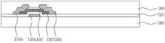
도 1은 일반적인 유기 발광 표시 장치의 단면도이다.1 is a cross-sectional view of a general organic light emitting diode display.
도 1과 같이, 일반적인 유기 발광 표시 장치는 기판(10)과, 기판(10) 상에 형성된 박막 트랜지스터, 박막 트랜지스터를 덮도록 형성된 보호막(16), 보호막(16) 상에 형성된 컬러 필터층(17), 컬러 필터층(17)을 덮도록 형성된 오버코트층(18) 및 오버코트층(18) 상에 형성된 유기 발광 표시 패널(20)을 포함하며, 유기 발광 표시 패널(20)은 차례로 적층된 제 1 전극(20a), 유기 발광층(20b), 제 2 전극(20c)을 포함한다.1, a general organic light emitting display includes a
박막 트랜지스터는 게이트 전극(11a), 게이트 절연막(12), 반도체층(13), 소스 전극(15a) 및 드레인 전극(15b)을 포함하며, 반도체층(13)이 산화물 반도체층인 경우, 반도체층(13) 상에 형성된 식각 차단층(Etch Stop Layer; ESL)(14)을 더 포함한다.The thin film transistor includes a
제 1 전극(20a)은 보호막(16)과 오버코트층(18)을 선택적으로 제거하여 형성된 드레인 콘택홀(미도시)을 통해 드레인 전극(15b)과 전기적으로 연결되며, 오버코트층(18) 상에 발광 영역을 정의하기 위해 제 1 전극(20a)의 일부를 노출시키는 뱅크홀을 갖는 뱅크(19)가 형성된다. 그리고, 뱅크홀에 유기 발광층(20b)이 형성되고, 유기 발광층(20b) 전면에 제 2 전극(20c)이 형성된다.The
상기와 같은 유기 발광 표시 패널(20)은 제 1 전극(20a)으로부터 정공이, 제 2 전극(20c)으로부터 전자가 주입되어, 유기 발광층(20b)으로 주입된 정공과 전자가 서로 결합할 때의 결합 에너지에 의해 발광한다. 또한, 유기 발광 표시 패널(20) 상에 유기 발광 표시 패널(20)을 캐핑하기 위한 인캡슐레이션층(Encapsulation Layer)이 더 형성될 수 있다.In the organic light
인캡슐레이션층은 글래스 캡(30)의 일 면에 형성된 페이스 씰(22)을 통해 유기 발광 표시 패널(20)상에 부착된다. 특히, 유기 발광층(20b)으로 수분 및 산소가 유입되는 것을 방지하기 위해 페이스 씰(22)과 유기 발광 표시 패널(20) 사이에 무기막(21)이 더 형성될 수 있다.The encapsulation layer is attached on the organic light
상기와 같은 유기 발광 표시 패널(20)은 유기 발광층(20b)에서 백색 광을 방출하는 경우 유기 발광층(20c)에서 발생된 백색 광이 각 서브 픽셀에 형성된 컬러 필터층(17)을 통과하며 다양한 색을 구현할 수 있다. 그런데, 유기 발광 표시 패널(20)에서 방출되는 광은 차례로 오버코트층(18), 컬러 필터층(17), 보호막(16), 게이트 절연막(12) 및 기판(10)을 통과하여 외부로 방출되므로, 높은 굴절률을 갖는 보호막(16)과 게이트 절연막(12)을 통과할 때 시야각에 따라 광 파장의 간섭 현상으로 인해 색 반전이 발생함에 따라, 시야각에 따라 색 좌표가 달라지는 문제가 발생한다.When the organic light
본 발명은 상기와 같은 문제점을 해결하기 위한 것으로, 유기 발광층에서 방출되는 광이 시야각에 따라 색 특성이 저하되는 것을 방지하기 위해, 발광 영역에 대응되는 고 굴절률의 게이트 절연막 및 보호막을 제거하여 컬러 필터를 통과한 광이 바로 기판을 통해 외부로 방출되는 유기 발광 표시 장치 및 이의 제조 방법을 제공하는데, 그 목적이 있다.SUMMARY OF THE INVENTION The present invention has been made in order to solve the above-mentioned problems, and it is an object of the present invention to provide an organic electroluminescent display device, in which a gate insulating film and a protective film, And a method of manufacturing the organic light emitting display device.
상기와 같은 목적을 달성하기 위한 본 발명의 유기 발광 표시 장치는 기판; 상기 기판 상에 형성된 박막 트랜지스터; 상기 박막 트랜지스터를 덮도록 형성된 보호막; 상기 기판의 표시 영역의 일부 영역에 대응되는 상기 박막 트랜지스터의 게이트 절연막과 상기 보호막을 제거하여 노출된 상기 기판 상에 형성된 컬러 필터층; 상기 컬러 필터층 및 보호막을 덮도록 상기 기판 전면에 형성된 오버코트층; 상기 보호막과 상기 오버코트층을 선택적으로 제거하여 상기 박막 트랜지스터를 노출시키는 드레인 콘택홀; 및 상기 오버코트층 상에 형성되며, 상기 드레인 콘택홀을 통해 상기 박막 트랜지스터와 접속하는 제 1 전극, 상기 제 1 전극 상에 형성된 백색 유기 발광층 및 상기 백색 유기 발광층을 덮도록 형성된 제 2 전극을 포함하는 유기 발광 표시 패널을 포함한다.According to an aspect of the present invention, there is provided an OLED display including: a substrate; A thin film transistor formed on the substrate; A protective film formed to cover the thin film transistor; A color filter layer formed on the exposed substrate by removing the gate insulating layer and the protective layer of the thin film transistor corresponding to a part of the display region of the substrate; An overcoat layer formed on the entire surface of the substrate to cover the color filter layer and the protective film; A drain contact hole for selectively removing the protective film and the overcoat layer to expose the thin film transistor; And a second electrode formed on the overcoat layer, the first electrode connected to the thin film transistor through the drain contact hole, the white organic light emitting layer formed on the first electrode, and the second electrode covering the white organic light emitting layer And an organic light emitting display panel.
상기 유기 발광 표시 패널에서 방출되는 백색 광은 차례로 상기 오버코트층, 컬러 필터층 및 기판을 통해 방출된다.The white light emitted from the organic light emitting display panel is sequentially emitted through the overcoat layer, the color filter layer, and the substrate.
상기 컬러 필터층과 상기 오버코트층의 굴절률은 동일하다.The refractive index of the color filter layer and the refractive index of the overcoat layer are the same.
상기 게이트 절연막 및 보호막의 굴절률은 상기 기판과 컬러 필터층의 굴절률보다 높다.The refractive index of the gate insulating film and the protective film is higher than the refractive index of the substrate and the color filter layer.
상기 기판의 표시 영역에 형성된 상기 보호막의 가장자리와 상기 게이트 절연막의 가장자리가 일치한다.The edge of the protective film formed on the display region of the substrate and the edge of the gate insulating film coincide with each other.
상기 게이트 절연막과 상기 보호막은 동일 물질로 형성된다.The gate insulating film and the protective film are formed of the same material.
또한, 동일 목적을 달성하기 위한 본 발명의 유기 발광 표시 장치의 제조 방법은 기판 상에 박막 트랜지스터를 형성하는 단계;According to another aspect of the present invention, there is provided a method of manufacturing an organic light emitting diode display, including: forming a thin film transistor on a substrate;
상기 박막 트랜지스터를 덮도록 상기 기판 전면에 보호막을 형성하는 단계; 상기 박막 트랜지스터의 게이트 절연막과 상기 보호막을 선택적으로 제거하여 상기 기판의 표시 영역의 일부 영역을 노출시키며, 동시에 상기 보호막을 선택적으로 제거하여 상기 박막 트랜지스터를 노출시키는 드레인 콘택홀 패턴을 형성하는 단계;Forming a protective film on the entire surface of the substrate so as to cover the thin film transistor; Selectively removing the gate insulating layer and the protective layer of the thin film transistor to expose a portion of the display region of the substrate and selectively removing the protective layer to form a drain contact hole pattern exposing the thin film transistor;
노출된 상기 기판 상에 컬러 필터층을 형성하는 단계; 상기 컬러 필터층 및 보호막을 덮도록 상기 기판 전면에 오버코트층을 형성하는 단계; 상기 드레인 콘택홀 패턴을 따라 상기 오버코트층을 선택적으로 제거하여 상기 박막 트랜지스터를 노출시키는 드레인 콘택홀을 형성하는 단계; 및 상기 오버코트층 상에 상기 드레인 콘택홀을 통해 상기 박막 트랜지스터와 접속하는 제 1 전극, 상기 제 1 전극 상에 형성된 백색 유기 발광층 및 상기 백색 유기 발광층을 덮도록 형성된 제 2 전극을 포함하는 유기 발광 표시 패널을 형성하는 단계를 포함한다.Forming a color filter layer on the exposed substrate; Forming an overcoat layer on the entire surface of the substrate so as to cover the color filter layer and the protective film; Forming a drain contact hole exposing the thin film transistor by selectively removing the overcoat layer along the drain contact hole pattern; And an organic light emitting display including a first electrode connected to the thin film transistor through the drain contact hole on the overcoat layer, a white organic light emitting layer formed on the first electrode, and a second electrode formed to cover the white organic light emitting layer. And forming a panel.
상기 유기 발광 표시 패널에서 방출되는 백색 광은 차례로 상기 오버코트층, 컬러 필터층 및 기판을 통해 방출된다.The white light emitted from the organic light emitting display panel is sequentially emitted through the overcoat layer, the color filter layer, and the substrate.
상기 기판의 표시 영역에 형성된 상기 보호막의 가장자리와 상기 게이트 절연막의 가장자리가 일치하도록 상기 게이트 절연막과 상기 보호막을 선택적으로 제거한다.The gate insulating film and the protective film are selectively removed so that the edges of the protective film formed on the display region of the substrate and the edges of the gate insulating film are aligned with each other.
상기 게이트 절연막과 상기 보호막은 동일 물질로 형성한다.The gate insulating film and the protective film are formed of the same material.
상기 박막 트랜지스터의 게이트 절연막과 상기 보호막을 선택적으로 제거하여 상기 기판의 표시 영역의 일부 영역을 노출시키며, 동시에 상기 보호막을 선택적으로 제거하여 상기 박막 트랜지스터를 노출시키는 드레인 콘택홀 패턴을 형성하는 단계는 하프톤 마스크(Half Tone Mask)를 이용한다.The step of selectively removing the gate insulating layer and the protective layer of the thin film transistor to expose a portion of the display region of the substrate and selectively removing the protective layer to form a drain contact hole pattern exposing the thin film transistor, Use a tone mask (Half Tone Mask).
상기와 같은 본 발명의 유기 발광 표시 장치는 다음과 같은 효과가 있다.The organic light emitting display of the present invention as described above has the following effects.
첫째, 표시 영역의 일부 영역에 대응되는 게이트 절연막 및 보호막을 제거하여 기판을 노출시키고, 노출된 기판 상에 바로 컬러 필터층을 형성함으로써, 유기 발광 표시 패널에서 방출되는 광이 고 굴절률의 게이트 절연막 및 보호막을 통과하지 않고, 굴절률이 유사한 오버코트층, 컬러 필터층 및 기판을 통과하여 외부로 방출됨에 따라 시야각에 따라 색 특성이 저하되는 것을 방지할 수 있다.First, the substrate is exposed by removing the gate insulating film and the protective film corresponding to a part of the display region, and the color filter layer is immediately formed on the exposed substrate. Thus, light emitted from the organic light emitting display panel has a high refractive index, It is possible to prevent the color characteristic from being degraded according to the viewing angle as the refractive index is passed through the overcoat layer, the color filter layer, and the substrate and is emitted to the outside.
둘째, 게이트 절연막 및 보호막을 제거하는 공정은 드레인 전극을 노출시키기 위한 공정과 동시에 수행되므로, 추가적인 마스크 공정 없이 색 특성이 저하되는 것을 방지할 수 있다.Secondly, the process of removing the gate insulating film and the protective film is performed simultaneously with the process of exposing the drain electrode, so that deterioration of the color characteristic without an additional mask process can be prevented.
도 1은 일반적인 유기 발광 표시 장치의 단면도.
도 2는 본 발명의 유기 발광 표시 장치의 단면도.
도 3a 내지 도 3l은 본 발명의 유기 발광 표시 장치의 제조 방법을 나타낸 공정 단면도.
도 4a는 일반적인 유기 발광 표시 장치의 시야각에 따른 색 특성을 나타낸 그래프이며, 도 4b는 본 발명의 유기 발광 표시 장치의 시야각에 따른 색 특성을 나타낸 그래프.1 is a sectional view of a general organic light emitting display device.
2 is a cross-sectional view of an organic light emitting display device according to the present invention.
FIGS. 3A to 3L are cross-sectional views illustrating a method of manufacturing an organic light emitting diode display according to the present invention.
FIG. 4A is a graph showing color characteristics according to viewing angles of a general organic light emitting display, and FIG. 4B is a graph showing color characteristics according to viewing angles of the organic light emitting display of the present invention.
이하, 첨부된 도면을 참조하여 본 발명의 유기 발광 표시 장치 및 이의 제조 방법을 상세히 설명하면 다음과 같다.Hereinafter, an organic light emitting display device and a method of manufacturing the same according to the present invention will be described in detail with reference to the accompanying drawings.
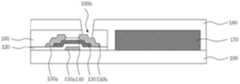
도 2는 본 발명의 유기 발광 표시 장치의 단면도이다.2 is a cross-sectional view of the organic light emitting diode display of the present invention.
도 2와 같이, 본 발명의 유기 발광 표시 장치는 기판(100) 상에 형성된 박막 트랜지스터, 박막 트랜지스터를 덮도록 형성된 보호막(160), 박막 트랜지스터의 게이트 절연막(120) 및 보호막(160)을 제거하여 노출된 기판(100) 상에 바로 형성된 컬러 필터층(170), 컬러 필터층(170) 및 보호막(160)을 덮도록 기판(100) 전면에 형성된 오버코트층(180) 및 오버코트층(180) 상에 형성된 유기 발광 표시 패널(200)을 포함한다.2, the OLED display of the present invention includes a thin film transistor formed on a
상기와 같은 박막 트랜지스터와 유기 발광 표시 패널(200)은 기판(100)의 표시 영역에 형성되며, 도시하지는 않았으나, 기판(100)의 비 표시 영역에는 게이트 배선과 접속된 게이트 패드 및 데이터 배선과 접속된 데이터 패드가 구비된다.The thin film transistor and the
구체적으로, 기판(100)의 표시 영역에는 게이트 절연막(120)을 사이에 두고 게이트 배선(미도시)과 데이터 배선(미도시)이 교차하여 복수 개의 서브 픽셀이 정의되고, 게이트 배선(미도시)과 데이터 배선(미도시)의 교차 영역에 박막 트랜지스터가 형성된다.More specifically, a plurality of subpixels are defined in the display region of the
박막 트랜지스터는 반도체층으로 IGZO(Indium Galium Zinc Oxide), ZnO(Zinc Oxide), TiO(Titanium Oxide)등의 산화물을 사용하는 박막 트랜지스터인 산화물 박막 트랜지스터(Oxide TFT), 반도체층으로 유기물을 사용하는 유기 박막 트랜지스터(Organic TFT), 반도체층으로 비정질 실리콘을 이용해 박막 트랜지스터 기판을 제조하는 비정질 실리콘 박막 트랜지스터(Amorphous Silicon TFT) 및 반도체층으로 다결정 실리콘을 이용해 박막 트랜지스터 기판을 제조하는 다결정 실리콘 박막 트랜지스터(Poly Silicon TFT) 중 하나가 선택되어 이루어지며, 도면에서는 산화물 박막 트랜지스터를 도시하였다.Thin film transistors are oxide thin film transistors (oxide TFTs) using oxide such as IGZO (Indium Gallium Zinc Oxide), ZnO (Zinc Oxide) and TiO (Titanium Oxide) as a semiconductor layer, organic thin film transistors An amorphous silicon TFT for forming a thin film transistor substrate using amorphous silicon as a semiconductor layer and a polycrystalline silicon thin film transistor for fabricating a thin film transistor substrate using a polycrystalline silicon as a semiconductor layer, TFT) is selected, and an oxide thin film transistor is shown in the drawing.
산화물 박막 트랜지스터는 실리콘 반도체층을 포함하는 실리콘 박막 트랜지스터(Silicon TFT)보다 높은 전하 이동도 및 낮은 누설전류 특성의 장점을 갖는다. 더욱이, 실리콘 박막 트랜지스터는 고온 공정을 통해 형성되며, 산화물 반도체층에 결정화 공정을 실시하므로, 대면적화 할수록 결정화 공정 시 균일도가 떨어져 대면적화에 불리하다. 그러나, 산화물 박막 트랜지스터는 저온 공정이 가능하며, 대면적화에 유리하다.The oxide thin film transistor has advantages of a higher charge mobility and a lower leakage current characteristic than a silicon thin film transistor (Silicon TFT) including a silicon semiconductor layer. Furthermore, since the silicon thin film transistor is formed through a high-temperature process and the crystallization process is performed on the oxide semiconductor layer, uniformity in the crystallization process is deteriorated as the size of the oxide semiconductor layer is increased. However, the oxide thin film transistor is capable of a low-temperature process, and is advantageous in large-area.
구체적으로, 산화물 박막 트랜지스터는 게이트 배선(미도시)에서 돌출 형성되거나 게이트 배선(미도시)의 일부 영역으로 정의된 게이트 전극(110a), 게이트 전극(110a)을 덮으며, 표시 영역의 일부 영역에 대응되는 기판(100)을 노출시키도록 형성된 게이트 절연막(120), 게이트 절연막(120) 상에 형성되어 게이트 전극(110a)과 중첩되는 반도체층(130), 반도체층(130) 상에 형성된 식각 차단층(Etch Stop Layer; ESL)(140) 및 식각 차단층(140) 상에 형성되며, 데이터 배선(미도시)과 접속된 소스 전극(150a) 및 소스 전극(150a)과 이격 형성된 드레인 전극(150b)을 포함한다.Specifically, the oxide thin film transistor covers the
이 때, 박막 트랜지스터를 덮도록 형성된 보호막(160) 역시 표시 영역의 일부 영역에 대응되는 기판(100)을 노출시키도록 형성된다. 게이트 절연막(120)과 보호막(160)은 SiOx, SiNx, Al2O3등과 무기 물질로 형성된다. 특히, 게이트 절연막(120)과 보호막(160)은 동일 물질로 형성되는 것이 바람직하며, 표시 영역에 형성된 보호막(160)의 가장자리와 게이트 절연막(120)의 가장자리가 일치한다.At this time, the
각 서브 픽셀의 노출된 기판(100) 상에는 R, G, B 컬러 필터층(170)이 형성되어, R, G, B 서브 픽셀이 정의된다. 이 때, 컬러 필터층(170)의 두께가 너무 두꺼운 경우 광 투과율이 저하되고, 두께가 너무 얇은 경우 색 재현율이 저하되므로, 컬러 필터층(170)의 두께는 약 1㎛인 것이 바람직하다. 특히, 컬러 필터층(170)이 형성되지 않는 W 서브 픽셀 역시 보호막(160)과 게이트 절연막(120)이 표시 영역의 일부 영역에 대응되는 기판(100)이 노출되도록 형성된다.On the exposed
상기와 같이, 컬러 필터층(170)이 형성된 R, G, B 서브 픽셀은 컬러 필터층(170)을 통해 유기 발광층(200b)에서 방출되는 백색 광이 다양한 컬러를 구현한다. 그리고, 컬러 필터층(170)이 형성되지 않은 W 서브 픽셀은 유기 발광층(200b)에서 방출되는 백색 광을 그대로 구현한다.As described above, the R, G, and B sub-pixels having the
그리고, 컬러 필터층(170)과 보호막(160)을 포함한 기판(100) 전면에 오버코트층(180)이 형성된다. 오버코트층(180)은 컬러 필터층(170)이 형성된 R, G, B 서브 픽셀뿐만 아니라, 컬러 필터층(170)이 형성되지 않은 W 서브 픽셀의 전면에 형성된다. 특히, W 서브 픽셀에는 컬러 필터층(170)이 형성되지 않으므로, 오버코트층(180)은 노출된 기판(100)의 전면을 덮도록 형성된다.An
그리고, 오버코트층(180)과 보호막(160)을 선택적으로 제거하여 형성된 드레인 콘택홀(미도시)을 통해 드레인 전극(150b)이 노출된다. 오버코트층(180) 상에는 차례로 적층된 제 1 전극(200a), 유기 발광층(200b) 및 제 2 전극(200c)을 포함하는 유기 발광 표시 패널(200)이 형성된다. 구체적으로, 제 1 전극(200a)은 드레인 콘택홀(미도시)을 통해 노출된 드레인 전극(150b)과 전기적으로 접속된다. 제 1 전극(200a)은 양극(Anode)으로, 틴 옥사이드(Tin Oxide: TO), 인듐 틴 옥사이드(Indium Tin Oxide: ITO), 인듐 징크 옥사이드(Indium Zinc Oxide: IZO), 인듐 틴 징크 옥사이드(Indium Tin Zinc Oxide: ITZO) 등과 같은 투명 전도성 물질로 형성된다.The
제 1 전극(200a) 상에는 발광 영역을 정의하기 위해 제 1 전극(200a)의 일부 영역을 노출시키는 뱅크홀을 갖는 뱅크(190)가 형성되고, 뱅크홀에 백색 유기 발광 물질로 이루어진 유기 발광층(200b)이 형성된다. 그리고, 유기 발광층(200b) 상에 제 2 전극(200c)이 형성된다. 제 2 전극(200c)은 음극(Cathode)으로 알루미늄(Al)과 같은 반사성 금속 재질로 형성되어, 유기 발광층(200b)에서 생성된 광을 제 1 전극(200a)방향으로 반사시킨다.A
도시하지는 않았으나, 제 1 전극(200a)과 유기 발광층(200b) 사이에 정공 주입층과 정공 수송층이 더 형성될 수 있으며, 정공 주입층과 정공 수송층은 유기 발광층(200b)으로 정공이 잘 주입되도록 하기 위한 것이다. 그리고, 유기 발광층(200b)과 제 2 전극(200c) 사이에 전자 주입층과 전자 수송층이 더 형성될 수 있으며, 전자 주입층과 전자 수송층은 유기 발광층(200b)으로 전자가 잘 주입되도록 하기 위한 것이다.Although not shown, a hole injecting layer and a hole transporting layer may be further formed between the
상기와 같은 유기 발광 표시 패널(200)은 제 1 전극(200a)과 제 2 전극(200c) 사이에 전압을 인가하면 제 1 전극(200a)으로부터 정공(Hole)이 제 2 전극(200c)으로부터 전자(Electron)가 주입되어 유기 발광층(200b)에서 재결합하여 엑시톤(Exciton)이 생성된다. 그리고, 엑시톤이 기저상태로 떨어지면서 발광하며, 상술한 바와 같이, 유기 발광 표시 패널(200) 하부의 컬러 필터층(170)을 통과하면서 각 컬러 필터층(170)에 대응되는 광이 기판(100)을 통해 외부로 방출된다.When a voltage is applied between the
즉, 상기와 같은 본 발명의 유기 발광 표시 장치는 유기 발광층(200b)에서 방출되는 광이 오버코트층(180), 컬러 필터층(170) 및 기판(100)을 통해 바로 외부로 방출된다.That is, in the organic light emitting diode display of the present invention, light emitted from the organic
일반적인 유기 발광 표시 장치는 유기 발광층(200b)과 기판(100) 사이에 오버코트층(180), 컬러 필터층(170), 보호막(160) 및 게이트 절연막(120)이 구비된다. 그런데, 일반적으로 컬러 필터층(170), 오버코트층(180) 및 기판(100)의 굴절률은 약 1.3 내지 1.6이나, 게이트 절연막(120) 및 보호막(160)의 귤절율은 2.0 이상이므로, 시야각에 따라 색 좌표가 변해 색 특성이 저하되는 문제가 발생한다.In a general organic light emitting diode display device, an
그러나, 상기와 같은 본 발명의 유기 발광 표시 장치는 오버코트층(180)과 컬러 필터층(170) 사이에 고 굴절률의 무기 물질로 형성된 게이트 절연막(120) 및 보호막(160)을 제거하고 컬러 필터층(170)이 기판(100) 상에 바로 형성됨에 따라, 유기 발광층(200c)에서 방출되는 광이 굴절률이 유사한 오버코트층(180), 컬러 필터층(170) 및 기판(100)을 통과하여 외부로 방출되므로, 시야각에 따라 색 특성이 저하되는 것을 방지할 수 있다.However, in the organic light emitting diode display of the present invention, the
그리고, 유기 발광 표시 패널(200) 상에는 유기 발광 표시 패널(200)을 캐핑하기 위한 인캡슐레이션층이 더 형성될 수 있으며, 인캡슐레이션층은 글래스 캡(300)의 일 면에 형성된 페이스 씰(220)을 통해 유기 발광 표시 패널(200)상에 부착된다. 특히, 유기 발광층(200b)으로 수분 및 산소가 유입되는 것을 방지하기 위해 페이스 씰(220)과 유기 발광 표시 패널(200) 사이에 AlOx, SiNx, 금속막 등과 같은 무기막(210)이 더 형성될 수 있다.An encapsulation layer for capping the organic light emitting
한편, 도시하지는 않았으나, 게이트 패드는 게이트 전극(110a)과 동일 층에 형성된 게이트 패드 하부 전극, 게이트 절연막(120), 보호막(160) 및 오버코트층(180)을 선택적으로 제거하여 게이트 패드 하부 전극을 노출시키는 게이트 콘택홀 및 제 1 전극(200a)과 동일 층에 형성되어 노출된 게이트 패드 하부 전극과 전기적으로 접속된 게이트 패드 상부 전극을 포함한다.Although not shown, the gate pad selectively removes the gate pad lower electrode, the
그리고, 데이트 패드는 소스 전극(150a)과 동일 층에 형성된 데이터 패드 하부 전극, 보호막(160)과 오버코트층(180)을 선택적으로 제거하여 데이터 패드 하부 전극을 노출시키는 데이터 콘택홀 및 제 1 전극(200a)과 동일 층에 형성되어 노출된 데이터 패드 하부 전극과 전기적으로 접속된 데이터 패드 상부 전극을 포함한다.The data pad has a data contact hole for selectively removing the data pad lower electrode, the
이하, 본 발명의 유기 발광 표시 장치의 제조 방법을 구체적으로 설명하면 다음과 같다.Hereinafter, a method of manufacturing the organic light emitting display device of the present invention will be described in detail.
도 3a 내지 도 3l은 본 발명의 유기 발광 표시 장치의 제조 방법을 나타낸 공정 단면도이다.3A to 3L are cross-sectional views illustrating a method of manufacturing an organic light emitting display according to an embodiment of the present invention.
도 3a와 같이, 기판(100)의 표시 영역에 게이트 배선(미도시) 및 게이트 전극(110a)을 형성한다. 도시하지는 않았으나, 게이트 배선(미도시)의 일 끝단은 기판(100)의 비 표시 영역까지 연장 형성되어, 게이트 배선(미도시)의 일 끝단에 게이트 패드 하부 전극이 형성된다. 게이트 배선(미도시), 게이트 전극 및 게이트 패드 하부 전극(미도시)을 포함한 기판(100) 전면에 SiOx, SiNx, Al2O3등과 같은 무기 물질로 게이트 절연막(120)을 형성한다.As shown in Fig. 3A, a gate wiring (not shown) and a
이어, 도 3b와 같이, 게이트 절연막(120)을 사이에 두고 게이트 전극(110a)과 중첩되는 반도체층(130)을 형성하고, 반도체층(130) 상에 식각 차단층(Etch Stop Layer; ESL)(140)을 형성한다. 그리고, 복수 개의 서브 픽셀을 정의하기 위해 게이트 절연막(120)을 사이에 두고 게이트 배선(미도시)과 교차하는 데이터 배선(미도시)을 형성하고, 데이터 배선(미도시)과 연결된 소스 전극(150a) 및 소스 전극(150a)과 이격된 드레인 전극(150b)을 형성한다. 도시하지는 않았으나, 데이터 배선(미도시)의 일 끝단은 기판(100)의 비 표시 영역까지 연장 형성되어, 데이터 배선(미도시)의 일 끝단에 데이터 패드 하부 전극이 형성된다.3B, a
상기와 같이 형성된 박막 트랜지스터는 반도체층(130)으로 IGZO(Indium Galium Zinc Oxide), ZnO(Zinc Oxide), TiO(Titanium Oxide)등을 사용하는 산화물 박막 트랜지스터이며, 경우에 따라 박막 트랜지스터는 반도체층으로 유기물을 사용하는 유기 박막 트랜지스터(Organic TFT), 반도체층으로 비정질 실리콘을 이용해 박막 트랜지스터 기판을 제조하는 비정질 실리콘 박막 트랜지스터(Amorphous Silicon TFT) 및 반도체층으로 다결정 실리콘을 이용해 박막 트랜지스터 기판을 제조하는 다결정 실리콘 박막 트랜지스터(Poly Silicon TFT) 중 선택하여 이루어질 수 있다.The thin film transistor formed as described above is an oxide thin film transistor using IGZO (indium gallium zinc oxide), ZnO (zinc oxide), TiO (titanium oxide) or the like as the
이어, 도 3c와 같이, 박막 트랜지스터를 덮도록 기판(100)의 표시 영역 및 비 표시 영역을 포함한 전면에 SiOx, SiNx, Al2O3등과 같은 무기 물질로 보호막(160)을 형성한다. 이 때, 보호막(160)은 게이트 절연막(120)과 동일 물질로 형성되는 것이 바람직하다. 그리고, 도 3d와 같이, 게이트 절연막(120)과 보호막(160)을 선택적으로 제거하여 기판(100)의 비 표시 영역에 형성된 게이트 패드 하부 전극(미도시) 및 데이터 패드 하부 전극(미도시)을 노출시킨다. 동시에, 보호막(160)을 선택적으로 제거하여 드레인 전극(150b)을 노출시키는 드레인 콘택홀 패턴(160a)을 형성하며, 표시 영역의 일부 영역에 대응되는 기판(100)이 노출되도록 보호막(160)과 게이트 절연막(120)을 제거한다.Next, as shown in Figure 3c, in the front, including the display region and the non-display area of the
이 때, 보호막(160)과 게이트 절연막(120)은 도 3d와 같이, 투과 영역(A) 및 차단 영역(B)을 갖는 마스크(MASK)를 이용하여 형성된 포토 레지스트 패턴을 마스크로 이용하여 제거한다. 마스크(MASK)의 투과 영역(A)은 보호막(160)과 게이트 절연막(120)을 제거하고자 하는 영역 및 드레인 전극(150a)을 노출시키는 드레인 콘택홀 패턴을 형성하는 영역에 대응되며, 차단 영역(B)은 나머지 영역에 대응된다.At this time, the
구체적으로, 보호막(160) 상에 포토 레지스트(400)를 도포하고, 포토 레지스트(400) 상에 마스크(MASK)를 위치시킨다. 그리고, 마스크를 이용하여 포토 레지스트(400)를 노광 및 현상하여, 도 3e와 같이, 포토 레지스트 패턴(400a)을 형성한다. 이어, 포토 레지스트 패턴(400a)을 마스크로 이용하여 노출된 보호막(160)과 게이트 절연막(120)을 제거하여 표시 영역의 일부 영역에 대응되는 기판(100)을 노출시키며, 동시에 드레인 전극(150b)을 노출시키는 드레인 콘택홀 패턴(160a)을 형성한다. 이 때, 게이트 절연막(120)과 보호막(160)은 동일 물질로 형성되므로, 표시 영역에 남아있는 보호막(160)의 가장자리와 게이트 절연막(120)의 가장자리가 일치된다.Specifically, the
상기와 같이, 본 발명은 드레인 콘택홀 영역(160a)의 형성과 표시 영역의 일부 영역에 대응되는 기판(100)을 동시에 노출시킬 수 있으며, 보호막(160)과 게이트 절연막(120)을 하프톤 마스크(Half Tone Mask)를 이용하여 선택적으로 제거하는 경우, 표시 영역에 대응되는 기판(100) 상에 보호막(160)과 게이트 절연막(120)을 제거하여 기판(100)을 노출시킨 후, 드레인 전극(150a)을 노출시키는 드레인 콘택홀 패턴을 형성할 수 있다.As described above, the present invention can simultaneously expose the formation of the drain
그리고, 도 3f와 같이, 포토 레지스트 패턴(400a)을 제거한 후, 도 3g와 같이, 각 서브 픽셀의 노출된 기판(100) 상에 R, G, B 컬러 필터층(170)을 형성한다. R, G, B 컬러 필터층이 형성된 각 서브 픽셀은 R, G, B 서브 픽셀로 정의된다. 특히, 컬러 필터층(170)이 형성되지 않는 W 서브 픽셀 역시 보호막(160)과 게이트 절연막(120)이 표시 영역의 일부 영역에 대응되는 기판(100)이 노출되도록 제거된다.After the
상기와 같이, 컬러 필터층(170)이 형성된 R, G, B 서브 픽셀은 컬러 필터층(170)을 통해 후술할 유기 발광층에서 방출되는 백색 광이 다양한 컬러를 구현한다. 그리고, 컬러 필터층(170)이 형성되지 않은 W 서브 픽셀은 유기 발광층에서 방출되는 백색 광을 그대로 구현한다.As described above, the R, G, and B sub-pixels in which the
이어, 도 3h와 같이, 기판(100) 전면에 오버코트층(180)을 형성한다. 이 때, 오버코트층(180)은 컬러 필터층(170)이 형성된 R, G, B 서브 픽셀뿐만 아니라, 컬러 필터층(170)이 형성되지 않은 W 서브 픽셀의 전면에 형성된다. 특히, W 서브 픽셀에는 컬러 필터층(170)이 형성되지 않으므로, W 서브 픽셀의 오버코트층(180)은 노출된 기판(100)의 전면을 덮도록 형성된다.Next, as shown in FIG. 3H, an
그리고, 오버코트층(180)을 선택적으로 제거하여 표시 영역의 드레인 콘택홀 패턴(160a)을 따라 드레인 전극(150b)을 노출시키는 드레인 콘택홀(160b)을 형성한다. 동시에, 기판(100)의 비 표시 영역의 게이트 패드 하부 전극(미도시)을 노출시키는 게이트 콘택홀 및 데이터 패드 하부 전극을 노출시키는 데이터 콘택홀을 형성한다.The
상기와 같이, 드레인 전극(150b)과 게이트 패드 하부 전극(미도시) 및 데이터 패드 하부 전극(미도시)을 노출시키기 위해 오버코트층(180)과 보호막(160) 및 게이트 절연막(120)을 따로 패터닝하는 것은 오버코트층(180)과 보호막(160)을 같이 패터닝하는 경우, 보호막(160)이 역 테이퍼 형상으로 제거되어 후술할 제 1 전극과 드레인 전극(150b), 게이트 패드 상부 전극과 게이트 패드 하부 전극 및 데이터 패드 상부 전극과 데이터 패드 하부 전극의 접촉 불량이 발생할 수 있기 때문이다.The
이어, 도 3i와 같이, 오버코트층(180)을 포함한 기판(100) 전면에 틴 옥사이드(Tin Oxide: TO), 인듐 틴 옥사이드(Indium Tin Oxide: ITO), 인듐 징크 옥사이드(Indium Zinc Oxide: IZO), 인듐 틴 징크 옥사이드(Indium Tin Zinc Oxide: ITZO) 등과 같은 투명 전도성 물질을 증착하고 이를 패터닝하여, 드레인 전극(150b)과 접속되는 제 1 전극(200a)을 형성하고, 동시에 비 표시 영역에도 게이트 콘택홀(미도시)을 통해 노출된 게이트 패드 하부 전극(미도시)과 접속되는 게이트 패드 상부 전극(미도시) 및 데이터 콘택홀(미도시)을 통해 노출된 데이터 패드 하부 전극(미도시)과 접속되는 데이터 패드 상부 전극(미도시)을 형성한다.3I, tin oxide (IT), indium tin oxide (ITO), indium zinc oxide (IZO), and the like are formed on the entire surface of the
이어, 도 3j와 같이, 제 1 전극(200a) 상에 표시 영역의 발광 영역을 정의하기 위해 제 1 전극(200a)의 일부 영역을 노출시키는 뱅크홀을 갖는 뱅크(190)를 형성한다. 그리고, 도 3k와 같이, 뱅크홀을 통해 노출된 제 1 전극(200a) 상에 유기 발광층(200b)을 형성한다. 유기 발광층(200b)은 백색 유기 발광 물질로 형성되어, 유기 발광층(200b)에서 방출되는 백색 광은 오버코트층(180), 컬러 필터층(170) 및 기판(100)을 통과하여 외부로 방출된다. 그리고, 유기 발광층(200b)을 덮도록 제 2 전극(200c)을 형성한다. 제 2 전극(200c)은 음극(Cathode)으로 알루미늄(Al)과 같은 반사성 금속 재질로 형성되어, 유기 발광층(200b)에서 방출되는 백색 광을 제 1 전극(200a) 방향으로 반사시킨다.Next, as shown in FIG. 3J, a
도시하지는 않았으나, 제 1 전극(200a)과 유기 발광층(200b) 사이에 정공 주입층과 정공 수송층이 더 형성될 수 있으며, 정공 주입층과 정공 수송층은 유기 발광층(200b)으로 정공이 잘 주입되도록 하기 위한 것이다. 또한, 유기 발광층(200b)과 제 2 전극(200c) 사이에 전자 주입층과 전자 수송층이 더 형성될 수 있으며, 전자 주입층과 전자 수송층은 유기 발광층(200b)으로 전자가 잘 주입되도록 하기 위한 것이다.Although not shown, a hole injecting layer and a hole transporting layer may be further formed between the
상기와 같은 유기 발광 표시 패널(200)은 제 1 전극(200a)과 제 2 전극(200c) 사이에 전압을 인가하면 제 1 전극(200a)으로부터 정공(Hole)이 제 2 전극(200c)으로부터 전자(Electron)가 주입되어 유기 발광층(200b)에서 재결합하여 엑시톤(Exciton)이 생성된다. 그리고, 엑시톤이 기저상태로 떨어지면서 발광하며, 유기 발광 표시 패널(200) 하부의 컬러 필터층(170)을 통과하면서 각 컬러 필터층(170)에 대응되는 광이 기판(100)을 통해 외부로 방출된다.When a voltage is applied between the
그리고, 도 3l와 같이, 외부의 수분 및 산소가 유기 발광층(200b)으로 유입되는 것을 방지하기 위해, 제 2 전극(200c) 전면에 무기막(210)을 형성하고, 유기 발광 표시 패널(200)을 캐핑하기 위해, 글래스 캡(300)의 일면에 형성된 페이스 씰(220)을 무기막(210) 상에 부착한다.In order to prevent external moisture and oxygen from flowing into the organic
상기와 같은 본 발명의 유기 발광 표시 장치의 제조 방법은 추가적인 마스크 공정 없이 기판(100)을 노출시키고, 노출된 기판(100) 상에 컬러 필터층(170)을 바로 형성하므로, 유기 발광층(200c)에서 방출되는 광이 굴절률이 유사한 오버코트층(180), 컬러 필터층(170) 및 기판(100)만을 통과하여 외부로 방출되므로, 시야각에 따라 색 특성이 저하되는 것을 방지할 수 있다.The method of manufacturing an organic light emitting diode display of the present invention as described above exposes the
도 4a는 일반적인 유기 발광 표시 장치의 시야각에 따른 색 특성을 나타낸 그래프이며, 도 4b는 본 발명의 유기 발광 표시 장치의 시야각에 따른 색 특성을 나타낸 그래프이다.FIG. 4A is a graph showing color characteristics according to viewing angles of a general organic light emitting display, and FIG. 4B is a graph showing color characteristics according to viewing angles of the organic light emitting display of the present invention.
일반적인 유기 발광 표시 장치는 유기 발광층에서 방출되는 광이 차례로 오버코트층, 컬러 필터층, 보호막, 게이트 절연막 및 기판을 통과하여 외부로 방출되므로, 컬러 필터층을 통과한 광이 높은 굴절률을 갖는 보호막과 게이트 절연막을 통과하며 광 파장의 간섭 현상이 발생한다. 이로 인해, 도 4a와 같이, 시야각에 따라 색 좌표(CIE x, CIE y)가 달라져, 색 특성이 저하되는 문제가 발생한다.Since the light emitted from the organic light emitting layer is sequentially emitted to the outside through the overcoat layer, the color filter layer, the protective layer, the gate insulating layer, and the substrate in general organic light emitting display devices, light passing through the color filter layer has a high refractive index and a gate insulating layer And interference of light wavelength occurs. As a result, the color coordinates (CIE x, CIE y) vary depending on the viewing angle as shown in Fig. 4A, and the color characteristic is deteriorated.
그러나, 본 발명의 유기 발광 표시 장치는 오버코트층(180)과 컬러 필터층(170) 사이에 고 굴절률의 게이트 절연막(120) 및 보호막(160)을 제거하고 컬러 필터층(170)이 기판(100) 상에 바로 형성됨에 따라, 유기 발광층(200c)에서 방출되는 광이 굴절률이 유사한 오버코트층(180), 컬러 필터층(170) 및 기판(100)만을 통과하여 외부로 방출되므로, 도 4b와 같이, 시야각이 변해도 색 좌표(CIE x, CIE y)가 거의 일정하다. 따라서, 시야각에 따라 색 특성이 저하되는 것을 방지할 수 있다.However, in the OLED display of the present invention, the
한편, 이상에서 설명한 본 발명은 상술한 실시 예 및 첨부된 도면에 한정되는 것이 아니고, 본 발명의 기술적 사상을 벗어나지 않는 범위 내에서 여러 가지 치환, 변형 및 변경이 가능하다는 것이 본 발명이 속하는 기술분야에서 통상의 지식을 가진 자에게 있어 명백할 것이다.While the present invention has been described in connection with what is presently considered to be the most practical and preferred embodiment, it is to be understood that the invention is not limited to the disclosed embodiments, but, on the contrary, is intended to cover various modifications and equivalent arrangements included within the spirit and scope of the appended claims. Will be apparent to those of ordinary skill in the art.
100: 기판110a: 게이트 전극
120: 게이트 절연막130: 반도체층
140: 식각 차단층150a: 소스 전극
150b: 드레인 전극160: 보호막
160a: 드레인 콘택홀 패턴160b: 드레인 콘택홀
170: 컬러 필터층180: 오버코트층
190: 뱅크200: 유기 발광 표시 패널
200a: 제 1 전극200b: 유기 발광층
200c: 제 2 전극210: 무기막
220: 페이스 씰300: 글래스 캡
400: 포토 레지스트400a: 포토 레지스트 패턴100:
120: gate insulating film 130: semiconductor layer
140:
150b: drain electrode 160: protective film
160a: drain
170: Color filter layer 180: Overcoat layer
190: bank 200: organic light emitting display panel
200a:
200c: second electrode 210: inorganic film
220: Face seal 300: Glass cap
400:
Claims (13)
Translated fromKorean상기 박막 트랜지스터를 덮는 보호막;
상기 박막 트랜지스터의 게이트 절연막과 상기 보호막을 제거하여 노출된 상기 기판 상에 위치하고, 상기 박막 트랜지스터 및 상기 보호막과 이격되는 컬러 필터층;
상기 컬러 필터층 및 상기 보호막을 덮는 오버코트층; 및
상기 오버코트층 상에 위치하고, 상기 박막 트랜지스터와 접속하는 유기 발광 표시 패널을 포함하는 것을 특징으로 하는 유기 발광 표시 장치.A thin film transistor located on a substrate and including a gate electrode, a gate insulating film, a semiconductor layer, a source electrode, and a drain electrode;
A protective film covering the thin film transistor;
A color filter layer disposed on the exposed substrate by removing the gate insulating layer and the protective layer of the thin film transistor, the color filter layer being spaced apart from the thin film transistor and the protective layer;
An overcoat layer covering the color filter layer and the protective film; And
And an organic light emitting display panel disposed on the overcoat layer and connected to the thin film transistor.
상기 유기 발광 표시 패널은 상기 박막 트랜지스터와 접속하는 제 1 전극 및 상기 제 1 전극 상에 순서대로 적층된 백색 유기 발광층과 제 2 전극을 포함하되,
상기 백색 유기 발광층에서 방출되는 백색 광은 차례로 상기 오버코트층, 컬러 필터층 및 기판을 통해 방출되는 것을 특징으로 하는 유기 발광 표시 장치.The method according to claim 1,
Wherein the organic light emitting display panel includes a first electrode connected to the thin film transistor, and a white organic light emitting layer and a second electrode sequentially stacked on the first electrode,
Wherein the white light emitted from the white organic light emitting layer is sequentially emitted through the overcoat layer, the color filter layer, and the substrate.
상기 컬러 필터층과 상기 오버코트층의 굴절률은 동일한 것을 특징으로 하는 유기 발광 표시 장치.The method according to claim 1,
Wherein the color filter layer and the overcoat layer have the same refractive index.
상기 게이트 절연막의 굴절률 및 상기 보호막의 굴절률은 상기 기판의 굴절률 및 상기 컬러 필터층의 굴절률보다 높은 것을 특징으로 하는 유기 발광 표시 장치.The method according to claim 1,
Wherein the refractive index of the gate insulating layer and the refractive index of the protective layer are higher than the refractive index of the substrate and the refractive index of the color filter layer.
상기 컬러 필터층에 가까이 위치하는 상기 보호막의 가장자리와 상기 게이트 절연막의 가장자리가 일치하는 것을 특징으로 하는 유기 발광 표시 장치.The method according to claim 1,
And an edge of the protective film located close to the color filter layer and an edge of the gate insulating film coincide with each other.
상기 게이트 절연막과 상기 보호막은 동일 물질을 포함하는 것을 특징으로 하는 유기 발광 표시 장치.The method according to claim 1,
Wherein the gate insulating layer and the passivation layer comprise the same material.
상기 박막 트랜지스터를 덮는 보호막을 형성하는 단계;
상기 박막 트랜지스터의 게이트 절연막과 상기 보호막을 선택적으로 제거하여 상기 기판의 일부 영역을 노출시키는 단계;
상기 보호막을 선택적으로 제거하여 상기 박막 트랜지스터를 노출시키는 드레인 콘택홀 패턴을 형성하는 단계;
상기 게이트 절연막 및 상기 보호막에 의해 노출된 상기 기판의 상기 일부 영역 상에 컬러 필터층을 형성하는 단계;
상기 컬러 필터층 및 상기 보호막을 덮는 오버코트층을 형성하는 단계;
상기 드레인 콘택홀 패턴을 따라 상기 오버코트층을 선택적으로 제거하여 상기 박막 트랜지스터를 노출시키는 드레인 콘택홀을 형성하는 단계; 및
상기 오버코트층 상에 상기 드레인 콘택홀을 통해 상기 박막 트랜지스터와 접속하는 유기 발광 표시 패널을 형성하는 단계를 포함하는 것을 특징으로 하는 유기 발광 표시 장치의 제조 방법.Forming a thin film transistor including a gate electrode, a gate insulating film, a semiconductor layer, a source electrode, and a drain electrode on a substrate;
Forming a protective film covering the thin film transistor;
Selectively removing the gate insulating layer and the protective layer of the thin film transistor to expose a portion of the substrate;
Forming a drain contact hole pattern exposing the thin film transistor by selectively removing the protective film;
Forming a color filter layer on the part of the substrate exposed by the gate insulating film and the protective film;
Forming an overcoat layer covering the color filter layer and the protective film;
Forming a drain contact hole exposing the thin film transistor by selectively removing the overcoat layer along the drain contact hole pattern; And
And forming an organic light emitting display panel on the overcoat layer, the organic light emitting display panel being connected to the thin film transistor through the drain contact hole.
상기 유기 발광 표시 패널은 상기 오버 코트층 상에 순서대로 적층된 제 1 전극, 백색 유기 발광층 및 제 2 전극을 포함하되,
상기 백색 유기 발광층에서 방출되는 백색 광은 차례로 상기 오버코트층, 컬러 필터층 및 기판을 통해 방출되는 것을 특징으로 하는 유기 발광 표시 장치의 제조 방법.8. The method of claim 7,
Wherein the organic light emitting display panel includes a first electrode, a white organic light emitting layer, and a second electrode sequentially stacked on the overcoat layer,
Wherein the white light emitted from the white organic light emitting layer is sequentially emitted through the overcoat layer, the color filter layer, and the substrate.
상기 게이트 절연막과 상기 보호막을 선택적으로 제거하는 단계는 상기 보호막의 가장자리와 상기 게이트 절연막의 가장자리를 일치시키는 단계를 포함하는 것을 특징으로 하는 유기 발광 표시 장치의 제조 방법.8. The method of claim 7,
Wherein the step of selectively removing the gate insulating layer and the passivation layer includes the step of aligning an edge of the passivation layer and an edge of the gate insulating layer.
상기 게이트 절연막과 상기 보호막은 동일 물질로 형성하는 것을 특징으로 하는 유기 발광 표시 장치의 제조 방법.8. The method of claim 7,
Wherein the gate insulating layer and the passivation layer are formed of the same material.
상기 기판의 상기 일부 영역을 노출시키는 단계 및 상기 드레인 콘택홀 패턴을 형성하는 단계는 하프톤 마스크(Half Tone Mask)를 이용하여 동시에 수행되는 것을 특징으로 하는 유기 발광 표시 장치의 제조 방법.8. The method of claim 7,
Wherein the step of exposing the partial area of the substrate and the step of forming the drain contact hole pattern are performed simultaneously using a half tone mask.
상기 컬러 필터층은 상기 기판과 직접 접촉하는 것을 특징으로 하는 유기 발광 표시 장치.The method according to claim 1,
Wherein the color filter layer is in direct contact with the substrate.
상기 컬러 필터층은 상기 기판의 상기 일부 영역과 직접 접촉하는 것을 특징으로 하는 유기 발광 표시 장치의 제조 방법.8. The method of claim 7,
Wherein the color filter layer is in direct contact with the partial area of the substrate.
Priority Applications (3)
| Application Number | Priority Date | Filing Date | Title |
|---|---|---|---|
| KR1020120091765AKR101908514B1 (en) | 2012-08-22 | 2012-08-22 | Organic light emitting display device and method for fabricating the same |
| US13/721,319US8895971B2 (en) | 2012-08-22 | 2012-12-20 | Organic light emitting display device and method for fabricating the same |
| CN201210573137.7ACN103633110B (en) | 2012-08-22 | 2012-12-26 | Organic light emitting display device and method for fabricating the same |
Applications Claiming Priority (1)
| Application Number | Priority Date | Filing Date | Title |
|---|---|---|---|
| KR1020120091765AKR101908514B1 (en) | 2012-08-22 | 2012-08-22 | Organic light emitting display device and method for fabricating the same |
Publications (2)
| Publication Number | Publication Date |
|---|---|
| KR20140025728A KR20140025728A (en) | 2014-03-05 |
| KR101908514B1true KR101908514B1 (en) | 2018-10-17 |
Family
ID=50147190
Family Applications (1)
| Application Number | Title | Priority Date | Filing Date |
|---|---|---|---|
| KR1020120091765AActiveKR101908514B1 (en) | 2012-08-22 | 2012-08-22 | Organic light emitting display device and method for fabricating the same |
Country Status (3)
| Country | Link |
|---|---|
| US (1) | US8895971B2 (en) |
| KR (1) | KR101908514B1 (en) |
| CN (1) | CN103633110B (en) |
Cited By (1)
| Publication number | Priority date | Publication date | Assignee | Title |
|---|---|---|---|---|
| KR20200064656A (en)* | 2018-11-29 | 2020-06-08 | 엘지디스플레이 주식회사 | Display apparatus having color filters and light-shielding element |
Families Citing this family (15)
| Publication number | Priority date | Publication date | Assignee | Title |
|---|---|---|---|---|
| KR101994227B1 (en) | 2012-12-07 | 2019-09-30 | 엘지디스플레이 주식회사 | Organic light emitting diode device and method for fabricating the same |
| KR20140077626A (en)* | 2012-12-14 | 2014-06-24 | 삼성디스플레이 주식회사 | Organic light emitting display apparatus |
| KR102120889B1 (en)* | 2013-05-21 | 2020-06-10 | 삼성디스플레이 주식회사 | Organic light emitting display apparatus and method for manufacturing the same |
| CN112992992A (en)* | 2014-10-01 | 2021-06-18 | 索尼公司 | Display device and electronic apparatus |
| KR102244758B1 (en)* | 2014-10-27 | 2021-04-28 | 삼성디스플레이 주식회사 | Display panel and method of manufacturing the same |
| CN104576700B (en)* | 2014-12-29 | 2017-11-03 | 深圳市华星光电技术有限公司 | COA type WOLED structures and preparation method |
| KR102442415B1 (en) | 2015-04-28 | 2022-09-13 | 삼성디스플레이 주식회사 | Organic light emitting diode display |
| KR102567547B1 (en)* | 2016-03-22 | 2023-08-17 | 삼성디스플레이 주식회사 | Display device |
| JP2017208253A (en)* | 2016-05-19 | 2017-11-24 | 株式会社ジャパンディスプレイ | Display device |
| KR102649202B1 (en)* | 2016-05-31 | 2024-03-20 | 엘지디스플레이 주식회사 | Organic Light Emitting Display device having an organic light emitting layer extending a non-display area |
| CN111048689B (en)* | 2016-06-30 | 2022-10-28 | 乐金显示有限公司 | Organic light emitting display device |
| KR102374754B1 (en)* | 2017-09-27 | 2022-03-15 | 엘지디스플레이 주식회사 | Display device having a touch structure |
| JP6935915B2 (en)* | 2017-10-27 | 2021-09-15 | 株式会社Joled | Electronic device |
| US11163203B2 (en)* | 2019-12-06 | 2021-11-02 | Tcl China Star Optoelectronics Technology Co., Ltd. | COA substrate and method of fabricating same |
| KR20230022307A (en)* | 2021-08-04 | 2023-02-15 | 삼성디스플레이 주식회사 | Light-emitting device and electronic apparatus including the same |
Citations (3)
| Publication number | Priority date | Publication date | Assignee | Title |
|---|---|---|---|---|
| KR100703158B1 (en)* | 2005-10-24 | 2007-04-06 | 삼성전자주식회사 | Display device and manufacturing method |
| JP2007127752A (en)* | 2005-11-02 | 2007-05-24 | Seiko Epson Corp | Electro-optical device manufacturing method, electro-optical device, and electronic apparatus |
| JP2009301002A (en) | 2008-06-12 | 2009-12-24 | Lg Display Co Ltd | Array substrate for liquid crystal display device, and manufacturing method thereof |
Family Cites Families (8)
| Publication number | Priority date | Publication date | Assignee | Title |
|---|---|---|---|---|
| US6512504B1 (en)* | 1999-04-27 | 2003-01-28 | Semiconductor Energy Laborayory Co., Ltd. | Electronic device and electronic apparatus |
| KR101098343B1 (en)* | 2004-06-03 | 2011-12-26 | 삼성전자주식회사 | Electro-luminescent display device, color filter panel and method for manufacturing there of |
| KR101447044B1 (en)* | 2006-10-31 | 2014-10-06 | 가부시키가이샤 한도오따이 에네루기 켄큐쇼 | Semiconductor device |
| JP2008276212A (en)* | 2007-04-05 | 2008-11-13 | Fujifilm Corp | Organic electroluminescence display |
| KR101910451B1 (en)* | 2008-07-10 | 2018-10-22 | 가부시키가이샤 한도오따이 에네루기 켄큐쇼 | Light-emitting device and electronic device using the same |
| KR101002662B1 (en)* | 2008-12-10 | 2010-12-20 | 삼성모바일디스플레이주식회사 | Organic light emitting display and manufacturing method thereof |
| KR101294853B1 (en)* | 2010-10-21 | 2013-08-08 | 엘지디스플레이 주식회사 | Organic Light Emitting Display Device |
| KR20120077470A (en)* | 2010-12-30 | 2012-07-10 | 삼성모바일디스플레이주식회사 | Organic light emitting diode display and fabricating method of the same |
- 2012
- 2012-08-22KRKR1020120091765Apatent/KR101908514B1/enactiveActive
- 2012-12-20USUS13/721,319patent/US8895971B2/enactiveActive
- 2012-12-26CNCN201210573137.7Apatent/CN103633110B/enactiveActive
Patent Citations (3)
| Publication number | Priority date | Publication date | Assignee | Title |
|---|---|---|---|---|
| KR100703158B1 (en)* | 2005-10-24 | 2007-04-06 | 삼성전자주식회사 | Display device and manufacturing method |
| JP2007127752A (en)* | 2005-11-02 | 2007-05-24 | Seiko Epson Corp | Electro-optical device manufacturing method, electro-optical device, and electronic apparatus |
| JP2009301002A (en) | 2008-06-12 | 2009-12-24 | Lg Display Co Ltd | Array substrate for liquid crystal display device, and manufacturing method thereof |
Cited By (2)
| Publication number | Priority date | Publication date | Assignee | Title |
|---|---|---|---|---|
| KR20200064656A (en)* | 2018-11-29 | 2020-06-08 | 엘지디스플레이 주식회사 | Display apparatus having color filters and light-shielding element |
| KR102656240B1 (en)* | 2018-11-29 | 2024-04-09 | 엘지디스플레이 주식회사 | Display apparatus having color filters and light-shielding element |
Also Published As
| Publication number | Publication date |
|---|---|
| US20140054555A1 (en) | 2014-02-27 |
| KR20140025728A (en) | 2014-03-05 |
| US8895971B2 (en) | 2014-11-25 |
| CN103633110A (en) | 2014-03-12 |
| CN103633110B (en) | 2017-04-12 |
Similar Documents
| Publication | Publication Date | Title |
|---|---|---|
| KR101908514B1 (en) | Organic light emitting display device and method for fabricating the same | |
| US11974453B2 (en) | Display device with block members having different heights | |
| US10930887B2 (en) | Flexible organic light emitting display device having a dam in a folding region | |
| US10170525B2 (en) | Organic light emitting display device | |
| KR101994227B1 (en) | Organic light emitting diode device and method for fabricating the same | |
| KR101920766B1 (en) | Method of fabricating the organic light emitting device | |
| KR101992917B1 (en) | Substrate for display, organic light emitting display device including the same, and method of manufacturing the same | |
| KR100838090B1 (en) | OLED display and manufacturing method thereof | |
| KR102441558B1 (en) | Organic light-emitting display apparatus and method for manufacturing the same | |
| US11552152B2 (en) | Display device including a power supply voltage wiring having openings | |
| US9941338B2 (en) | Organic light-emitting diode display and method of manufacturing the same | |
| US20170077456A1 (en) | Display device | |
| EP3905359A1 (en) | Display panel and display apparatus including the same | |
| KR20190073636A (en) | Organic light emitting display device | |
| KR20170078909A (en) | Organic light emitting display device | |
| KR20220115709A (en) | Display panel and display apparatus including the same | |
| KR102247825B1 (en) | Bottom Emission Type Organic Light Emission Diode Display Having Color Filters And Method For Manufacturing The Same | |
| KR102009800B1 (en) | Organic light emitting display device and method for fabricating the same | |
| KR102086393B1 (en) | Organic light emitting display device and method for manufacturing thereof | |
| KR102053440B1 (en) | Organic Light Emitting Diode Display Having High Aperture Ratio And Method For Manufacturing The Same | |
| US11309512B2 (en) | Organic EL display device and method for manufacturing organic EL display device | |
| KR102612736B1 (en) | Substrate for display, organic light emitting display device including the same, and method of manufacturing the same | |
| KR102218944B1 (en) | Organic light emitting diode display device and method for fabricating the same | |
| KR102723113B1 (en) | Display Device And Method Of Fabricating The Same | |
| KR20130075427A (en) | Organic light emitting display device and method of fabricating the same |
Legal Events
| Date | Code | Title | Description |
|---|---|---|---|
| PA0109 | Patent application | St.27 status event code:A-0-1-A10-A12-nap-PA0109 | |
| PG1501 | Laying open of application | St.27 status event code:A-1-1-Q10-Q12-nap-PG1501 | |
| R17-X000 | Change to representative recorded | St.27 status event code:A-3-3-R10-R17-oth-X000 | |
| A201 | Request for examination | ||
| PA0201 | Request for examination | St.27 status event code:A-1-2-D10-D11-exm-PA0201 | |
| D13-X000 | Search requested | St.27 status event code:A-1-2-D10-D13-srh-X000 | |
| D14-X000 | Search report completed | St.27 status event code:A-1-2-D10-D14-srh-X000 | |
| E902 | Notification of reason for refusal | ||
| PE0902 | Notice of grounds for rejection | St.27 status event code:A-1-2-D10-D21-exm-PE0902 | |
| P11-X000 | Amendment of application requested | St.27 status event code:A-2-2-P10-P11-nap-X000 | |
| P13-X000 | Application amended | St.27 status event code:A-2-2-P10-P13-nap-X000 | |
| E701 | Decision to grant or registration of patent right | ||
| PE0701 | Decision of registration | St.27 status event code:A-1-2-D10-D22-exm-PE0701 | |
| GRNT | Written decision to grant | ||
| PR0701 | Registration of establishment | St.27 status event code:A-2-4-F10-F11-exm-PR0701 | |
| PR1002 | Payment of registration fee | St.27 status event code:A-2-2-U10-U11-oth-PR1002 Fee payment year number:1 | |
| PG1601 | Publication of registration | St.27 status event code:A-4-4-Q10-Q13-nap-PG1601 | |
| PR1001 | Payment of annual fee | St.27 status event code:A-4-4-U10-U11-oth-PR1001 Fee payment year number:4 | |
| PR1001 | Payment of annual fee | St.27 status event code:A-4-4-U10-U11-oth-PR1001 Fee payment year number:5 | |
| P22-X000 | Classification modified | St.27 status event code:A-4-4-P10-P22-nap-X000 | |
| P22-X000 | Classification modified | St.27 status event code:A-4-4-P10-P22-nap-X000 | |
| PR1001 | Payment of annual fee | St.27 status event code:A-4-4-U10-U11-oth-PR1001 Fee payment year number:6 | |
| PR1001 | Payment of annual fee | St.27 status event code:A-4-4-U10-U11-oth-PR1001 Fee payment year number:7 | |
| P22-X000 | Classification modified | St.27 status event code:A-4-4-P10-P22-nap-X000 | |
| PR1001 | Payment of annual fee | St.27 status event code:A-4-4-U10-U11-oth-PR1001 Fee payment year number:8 |