KR101908501B1 - Integrated Touch Screen With Organic Emitting Display Device and Method for Manufacturing the Same - Google Patents
Integrated Touch Screen With Organic Emitting Display Device and Method for Manufacturing the SameDownload PDFInfo
- Publication number
- KR101908501B1 KR101908501B1KR1020110130621AKR20110130621AKR101908501B1KR 101908501 B1KR101908501 B1KR 101908501B1KR 1020110130621 AKR1020110130621 AKR 1020110130621AKR 20110130621 AKR20110130621 AKR 20110130621AKR 101908501 B1KR101908501 B1KR 101908501B1
- Authority
- KR
- South Korea
- Prior art keywords
- layer
- touch
- substrate
- buffer layer
- touch electrode
- Prior art date
- Legal status (The legal status is an assumption and is not a legal conclusion. Google has not performed a legal analysis and makes no representation as to the accuracy of the status listed.)
- Active
Links
Images


Classifications
- G—PHYSICS
- G06—COMPUTING OR CALCULATING; COUNTING
- G06F—ELECTRIC DIGITAL DATA PROCESSING
- G06F3/00—Input arrangements for transferring data to be processed into a form capable of being handled by the computer; Output arrangements for transferring data from processing unit to output unit, e.g. interface arrangements
- G06F3/01—Input arrangements or combined input and output arrangements for interaction between user and computer
- G06F3/03—Arrangements for converting the position or the displacement of a member into a coded form
- G06F3/041—Digitisers, e.g. for touch screens or touch pads, characterised by the transducing means
- G06F3/0412—Digitisers structurally integrated in a display
- G—PHYSICS
- G02—OPTICS
- G02F—OPTICAL DEVICES OR ARRANGEMENTS FOR THE CONTROL OF LIGHT BY MODIFICATION OF THE OPTICAL PROPERTIES OF THE MEDIA OF THE ELEMENTS INVOLVED THEREIN; NON-LINEAR OPTICS; FREQUENCY-CHANGING OF LIGHT; OPTICAL LOGIC ELEMENTS; OPTICAL ANALOGUE/DIGITAL CONVERTERS
- G02F1/00—Devices or arrangements for the control of the intensity, colour, phase, polarisation or direction of light arriving from an independent light source, e.g. switching, gating or modulating; Non-linear optics
- G02F1/01—Devices or arrangements for the control of the intensity, colour, phase, polarisation or direction of light arriving from an independent light source, e.g. switching, gating or modulating; Non-linear optics for the control of the intensity, phase, polarisation or colour
- G02F1/13—Devices or arrangements for the control of the intensity, colour, phase, polarisation or direction of light arriving from an independent light source, e.g. switching, gating or modulating; Non-linear optics for the control of the intensity, phase, polarisation or colour based on liquid crystals, e.g. single liquid crystal display cells
- G02F1/133—Constructional arrangements; Operation of liquid crystal cells; Circuit arrangements
- G02F1/1333—Constructional arrangements; Manufacturing methods
- G02F1/13338—Input devices, e.g. touch panels
- H—ELECTRICITY
- H10—SEMICONDUCTOR DEVICES; ELECTRIC SOLID-STATE DEVICES NOT OTHERWISE PROVIDED FOR
- H10K—ORGANIC ELECTRIC SOLID-STATE DEVICES
- H10K59/00—Integrated devices, or assemblies of multiple devices, comprising at least one organic light-emitting element covered by group H10K50/00
- H10K59/10—OLED displays
- H10K59/12—Active-matrix OLED [AMOLED] displays
- H—ELECTRICITY
- H10—SEMICONDUCTOR DEVICES; ELECTRIC SOLID-STATE DEVICES NOT OTHERWISE PROVIDED FOR
- H10K—ORGANIC ELECTRIC SOLID-STATE DEVICES
- H10K59/00—Integrated devices, or assemblies of multiple devices, comprising at least one organic light-emitting element covered by group H10K50/00
- H10K59/40—OLEDs integrated with touch screens
- H—ELECTRICITY
- H10—SEMICONDUCTOR DEVICES; ELECTRIC SOLID-STATE DEVICES NOT OTHERWISE PROVIDED FOR
- H10K—ORGANIC ELECTRIC SOLID-STATE DEVICES
- H10K71/00—Manufacture or treatment specially adapted for the organic devices covered by this subclass
- H—ELECTRICITY
- H10—SEMICONDUCTOR DEVICES; ELECTRIC SOLID-STATE DEVICES NOT OTHERWISE PROVIDED FOR
- H10K—ORGANIC ELECTRIC SOLID-STATE DEVICES
- H10K71/00—Manufacture or treatment specially adapted for the organic devices covered by this subclass
- H10K71/80—Manufacture or treatment specially adapted for the organic devices covered by this subclass using temporary substrates
- G—PHYSICS
- G06—COMPUTING OR CALCULATING; COUNTING
- G06F—ELECTRIC DIGITAL DATA PROCESSING
- G06F2203/00—Indexing scheme relating to G06F3/00 - G06F3/048
- G06F2203/041—Indexing scheme relating to G06F3/041 - G06F3/045
- G06F2203/04103—Manufacturing, i.e. details related to manufacturing processes specially suited for touch sensitive devices
Landscapes
- Engineering & Computer Science (AREA)
- Physics & Mathematics (AREA)
- General Engineering & Computer Science (AREA)
- Theoretical Computer Science (AREA)
- General Physics & Mathematics (AREA)
- Human Computer Interaction (AREA)
- Manufacturing & Machinery (AREA)
- Microelectronics & Electronic Packaging (AREA)
- Nonlinear Science (AREA)
- Mathematical Physics (AREA)
- Chemical & Material Sciences (AREA)
- Crystallography & Structural Chemistry (AREA)
- Optics & Photonics (AREA)
- Electroluminescent Light Sources (AREA)
- Devices For Indicating Variable Information By Combining Individual Elements (AREA)
Abstract
Translated fromKoreanDescription
Translated fromKorean본 발명은 유기 발광 표시 장치에 관한 것으로 특히, 박막 가능하며 플렉서블한 형태로 구현이 가능한 터치 스크린 일체형 유기 발광 표시 장치 및 이의 제조 방법에 관한 것이다.BACKGROUND OF THE INVENTION 1. Field of the Invention The present invention relates to an organic light emitting diode display, and more particularly, to a touch screen integrated organic light emitting diode display capable of being formed in a thin and flexible form, and a method of manufacturing the same.
평판 표시장치의 구체적인 예로는 액정표시장치(Liquid Crystal Display device: LCD), 유기 발광 표시 장치(Organic Emitting Display Device), 플라즈마 표시장치(Plasma Display Panel device: PDP), 양자점 표시 장치(Quantum Dot Display Device), 전계방출표시장치(Field Emission Display device: FED), 전기영동 표시장치(Electrophoretic Display Device : EPD) 등을 들 수 있는데, 이들은 공통적으로 화상을 구현하는 평판 표시패널을 필수적인 구성요소로 하는 바, 평판 표시패널은 고유의 발광 또는 편광 혹은 그 밖의 광학 물질층을 사이에 두고 한 쌍의 투명 절연기판을 대면 합착시킨 구성을 갖는다.Specific examples of the flat panel display include a liquid crystal display (LCD) device, an organic light emitting display device, a plasma display panel (PDP) device, a quantum dot display device ), A field emission display device (FED), and an electrophoretic display device (EPD). The flat display panel, which realizes images in common, is an essential component, The flat panel display panel has a structure in which a pair of transparent insulation substrates are bonded together with inherent light emission, polarization, or other optical material layers interposed therebetween.
이 중 유기 발광 표시장치는 최근 표시장치의 대형화에 따라 공간 점유가 적은 평면표시소자의 요구가 증대되고 있는데, 이러한 평면표시소자 중 하나로서 유기발광다이오드(organic light emitting diode: OLED)라고도 불리는 유기 전계 발광 소자의 기술이 빠른 속도로 발전하고 있으며, 이미 여러 시제품들이 발표된 바 있다.Among these organic light emitting display devices, the demand for a flat display device with a small space occupation has been increasing with the recent enlargement of display devices. One of such flat display devices is an organic light emitting diode (OLED) The technology of the light emitting device is rapidly developing, and several prototypes have already been announced.
유기 발광 표시 장치는 별도의 광원을 요구치 않고, 내부에 픽셀 단위로 자발광의 유기 발광 다이오드를 포함하여 표시가 이루어지는 것으로, 광원 및 이를 표시 패널과 조립하기 위한 구조물이 생략되는 이점이 있어 차세대 표시 장치로 고려되고 있다.The organic light emitting display device does not require a separate light source and includes a self-luminous organic light emitting diode in a pixel unit in the inside thereof. Thus, a light source and a structure for assembling the light source with the display panel are omitted, .
상기 유기 발광 다이오드는 전자 주입 전극(음극) 과 정공 주입 전극(양극) 사이에 형성된 유기막에 전하를 주입하면 전자와 정공이 쌍을 이룬 후 소멸하면서 빛을 내는 소자이다.The organic light emitting diode is a device that injects an electric charge into an organic film formed between an electron injection electrode (cathode) and a hole injection electrode (anode) to form an electron and a hole.
한편, 이러한 표시 장치에, 사람의 손이나 별도의 입력 수단을 통해 터치 부위를 인식하고 이에 대응하여 별도의 정보를 전달할 수 있는 터치 스크린을 부가하는 요구가 늘고 있다. 현재 이러한 터치 스크린은 표시 장치의 외부 표면에 부착하는 형태로 적용되고 있다.On the other hand, there is a growing demand for a touch screen capable of recognizing a touch area through a human hand or a separate input device and transmitting additional information in response to such a display device. Currently, such a touch screen is applied in a form attached to an outer surface of a display device.
그리고, 터치 감지 방식에 따라, 저항 방식, 정전 용량 방식, 적외선 감지 방식 등으로 나뉘며, 제조 방식의 편이성 및 센싱력 등을 감안하여 소형 모델에 있어서는 최근 정전 용량 방식이 주목받고 있다.According to the touch sensing method, a resistance method, a capacitance method, and an infrared sensing method are categorized. Recently, in consideration of convenience of manufacturing method and sensing power, recently, a capacitance method is attracting attention.
이하, 도면을 참조하여 종래의 터치 스크린 부착형 유기 발광 표시 장치를 살펴본다.Hereinafter, a conventional touch screen type organic light emitting display will be described with reference to the drawings.
도 1은 종래의 터치 스크린 부착형 유기 발광 표시 장치를 나타낸 단면도이다.1 is a cross-sectional view of a conventional touch screen type organic light emitting display.
도 1과 같이, 종래의 터치 스크린 부착형 유기 발광 표시 장치는 아래에서부터 차례로, 유기 발광 표시 패널(10), 터치 스크린(20) 및 커버 윈도우(30)에 적층되어 있으며, 각 층 사이에 제 1, 제 2 접착층(15, 25)이 구비된다.As shown in FIG. 1, the conventional touch screen type organic light emitting display device is stacked on the organic light
여기서, 상기 유기 발광 표시 패널(10)은 기판과, 기판 상의 매트릭스 상의 배열을 갖는 박막 트랜지스터 어레이 및 박막 트랜지스터 어레이의 각 박막 트랜지스터와 접속된 유기 발광 다이오드를 포함하며, 유기 발광 다이오드의 상부를 덮도록 보호막 및 편광층이 구비된다. 이 경우, 상기 편광층 상에 제 1 접착층(15)이 대응되는 것이다.Here, the organic light
상기와 같은 종래의 터치 스크린 부착형 유기 발광 표시 장치는 다음과 같은 문제점이 있다.The conventional touch screen type OLED display has the following problems.
첫째, 각각 독립적으로 유기 발광 표시 패널과 터치 스크린을 형성 후 터치 스크린을 상기 유기 발광 표시 패널에 부착하는 경우, 터치 스크린의 보호를 위해 커버 글래스가 요구되며, 커버 글래스를 포함한 터치 스크린 및 유기 발광 표시 패널의 총 적층 두께가 두꺼워 박막화 및 플렉서블한 형태로 구현이 불가능하다.When a touch screen is attached to the organic light emitting display panel after forming the organic light emitting display panel and the touch screen independently of each other, a cover glass is required for protecting the touch screen, a touch screen including a cover glass, The total lamination thickness of the panel is so thick that it can not be realized in a thin and flexible form.
둘째, 유기 발광 표시 패널과 터치 스크린이 모두 개별적인 패널 형태를 가지기 때문에, 이를 형성하기 위한 공정이 복잡하고 이로 인해 수율이 저하되고 가격 경쟁력이 떨어진다.Second, since the organic light emitting display panel and the touch screen both have individual panel shapes, the processes for forming the organic light emitting display panel and the touch screen are complicated, resulting in lower yield and lower price competitiveness.
셋째, 완성된 유기 발광 표시 패널의 상부측에는 광학적으로 외부광을 차단하는 편광판이 구비되는 데, 이로 인해 그 상부에 터치 스크린 형성시 터치 스크린 내의 전극 패턴이 시인되는 문제점이 있다.Thirdly, a polarizing plate for optically blocking external light is provided on the upper side of the completed organic light emitting display panel, which causes a problem that the electrode pattern in the touch screen is visible when the touch screen is formed thereon.
본 발명은 상기와 같은 문제점을 해결하기 위해 안출한 것으로 박막 가능하며 플렉서블한 형태로 구현이 가능한 터치 스크린 일체형 유기 발광 표시 장치 및 이의 제조 방법을 제공하는 데, 그 목적이 있다.It is an object of the present invention to provide a touch screen integrated type organic light emitting display device and a method of manufacturing the same, which are thin and capable of being implemented in a flexible form.
상기와 같은 목적을 달성하기 위한 본 발명의 터치 스크린 일체형 유기 발광 표시 장치는 필름 기판;과, 상기 필름 기판 상에 차례로 형성된 제 1 에치 스토퍼층 및 제 1 버퍼층;과, 상기 제 1 버퍼층 상에 매트릭스 상으로 화소가 정의되며 각 화소별로 박막 트랜지스터를 갖는 박막 트랜지스터 어레이;와, 상기 각 화소의 박막 트랜지스터와 접속된 유기 발광 다이오드;와, 상기 박막 트랜지스터 어레이 및 유기 발광 다이오드를 덮는 보호층;과, 상기 보호층과 접한 터치 전극층;과, 상기 터치 전극층 상에 차례로 형성된 제 2 버퍼층 및 제 2 에치 스토퍼층; 및 상기 제 2 에치 스토퍼층 상에 형성된 편광판을 포함하여 이루어진 것에 그 특징이 있다.According to an aspect of the present invention, there is provided a touch screen integrated type organic light emitting diode (OLED) display comprising: a film substrate; a first etch stopper layer and a first buffer layer sequentially formed on the film substrate; And a protective layer covering the thin film transistor array and the organic light emitting diode, wherein the thin film transistor array includes a thin film transistor array, A second buffer layer and a second etch stopper layer sequentially formed on the touch electrode layer; And a polarizing plate formed on the second etch stopper layer.
여기서, 상기 필름 기판은 플라스틱 절연성 필름이다.Here, the film substrate is a plastic insulating film.
상기 제 1 에치 스토퍼층 및 제 2 에치 스토퍼층은 폴리 이미드 또는 포토 아크릴이다.The first etch stopper layer and the second etch stopper layer are polyimide or photoacrylic.
그리고, 상기 제 1 버퍼층 및 제 2 버퍼층은 복수층의 무기막으로 이루어질 수 있다. 예를 들어, 상기 복수층의 무기막은 SiNx 또는 SiO2의 연속 적층 또는 교번 적층으로 이루어질 수 있다.The first buffer layer and the second buffer layer may be formed of a plurality of inorganic films. For example, the plurality of inorganic films may consist of a continuous lamination or an alternating lamination of SiNx or SiO2.
또한, 상기 터치 전극층은 서로 교차하는 형상의 제 1 터치 전극 및 제 2 터치 전극과, 상기 제 1 및 제 2 터치 전극에 각각 신호를 전달하는 터치 패드 전극을 포함한다. 상기 터치 패드 전극은 상기 박막 트랜지스터 어레이와 동일층에 형성된 더미 금속과 접속될 수 있다. 이 경우, 상기 터치 패드 전극과 상기 더미 금속과의 접속은 금속 도전성 볼을 통해 이루어진다. 또한, 상기 금속 도전성 볼은 Au 또는 Ag를 포함한 것일 수 있다.The touch electrode layer includes a first touch electrode and a second touch electrode which intersect each other, and a touch pad electrode that transmits signals to the first and second touch electrodes. The touch pad electrode may be connected to a dummy metal formed on the same layer as the thin film transistor array. In this case, the connection between the touch pad electrode and the dummy metal is made through a metal conductive ball. In addition, the metal conductive ball may include Au or Ag.
한편, 상기 제 1 버퍼층은 상기 터치 전극층보다 외측으로 돌출된다. 상기 제 1 버퍼층의 상기 터치 전극층보다 돌출된 외측에 상기 제 1 터치 전극 및 제 2 터치 전극과 신호를 주고 받는 터치 구동 IC와, 상기 박막 트랜지스터 어레이 및 상기 유기 발광 다이오드에 신호를 전달하는 OLED IC를 갖는다.On the other hand, the first buffer layer protrudes outward from the touch electrode layer. A touch driving IC for transmitting and receiving signals to and from the first touch electrode and the second touch electrode on an outer side of the first buffer layer protruding from the touch electrode layer, and an OLED IC for transmitting a signal to the thin film transistor array and the organic light emitting diode .
여기서, 상기 터치 구동 IC와 상기 OLED IC은, 상기 제 1 버퍼층의 상기 터치 전극층보다 돌출된 외측 가장자리에 형성된 플렉서블 인쇄회로 기판과 연결된다.Here, the touch driving IC and the OLED IC are connected to a flexible printed circuit board formed on an outer edge of the first buffer layer protruding from the touch electrode layer.
또한, 상기 편광판 상에 커버 윈도우를 더 포함한다. 이 경우, 상기 커버 윈도우는 절연성 투명 필름인 것이 바람직하다.In addition, a cover window is further included on the polarizing plate. In this case, the cover window is preferably an insulating transparent film.
상기 제 1 버퍼층, 상기 제 1 에치 스토퍼층 및 상기 필름 기판은 동일한 제 1 크기이며, 상기 터치 전극층, 상기 제 2 버퍼층 및 상기 제 2 에치 스토퍼층은 동일한 제 2 크기이며, 상기 제 1 크기가 제 2 크기보다 큰 것이 바람직하다.Wherein the first buffer layer, the first etch stopper layer, and the film substrate have the same first size, the touch electrode layer, the second buffer layer, and the second etch stopper layer have the same second size, 2 size.
또한, 동일한 목적을 달성하기 위한 본 발명의 터치 스크린 일체형 유기 발광 표시 장치의 제조 방법은 제 1 기판 상에 제 1 에치 스토퍼층 및 제 1 버퍼층과, 상기 제 1 버퍼층 상에 매트릭스 상으로 화소가 정의되며 각 화소별로 박막 트랜지스터를 갖는 박막 트랜지스터 어레이 및 상기 각 화소의 박막 트랜지스터와 접속된 유기 발광 다이오드, 상기 박막 트랜지스터 어레이 및 유기 발광 다이오드를 덮는 보호층을 차례로 형성하는 단계;와, 제 2 기판 상에 제 2 에치 스토퍼층 및 제 2 버퍼층과, 상기 제 2 버퍼층 상에 터치 전극층을 차례로 형성하는 단계;와, 상기 터치 전극층을 상기 보호층에 대면하여 부착하는 단계;와, 상기 제 1 기판 및 제 2 기판을 제거하는 단계; 및 상기 제 1 에치 스토퍼층의 노출된 면에 필름 기판을 부착하는 단계를 포함하여 이루어진 것에 또 다른 특징이 있다.In another aspect of the present invention, there is provided a method of fabricating a touch screen integrated type organic light emitting diode display, comprising: forming a first etch stopper layer and a first buffer layer on a first substrate; Forming a thin film transistor array having a thin film transistor for each pixel, an organic light emitting diode connected to the thin film transistor of each pixel, a protective layer covering the thin film transistor array and the organic light emitting diode, A first buffer layer, a second buffer layer, a second buffer layer, a second buffer layer, a second buffer layer, a second buffer layer, a second buffer layer, a second buffer layer, and a touch electrode layer on the second buffer layer, Removing the substrate; And attaching the film substrate to the exposed surface of the first etch stopper layer.
또한, 상기 제 2 기판의 제거 후 노출된 상기 제 2 에치 스토퍼층의 면에 편광판을 부착하는 단계를 더 포함할 수 있다.The method may further include the step of attaching the polarizer to the surface of the second etch stopper layer exposed after the removal of the second substrate.
그리고, 상기 제 1 기판 및 제 2 기판을 제거하는 단계는 상기 제 1 기판과 제 2 기판을 식각하거나 레이저를 조사하여 이루어질 수 있다.The removing of the first substrate and the second substrate may be performed by etching the first substrate and the second substrate or by irradiating a laser beam.
상기 제 1 버퍼층 및 제 2 버퍼층의 형성은 SiNx 또는 SiO2의 연속 적층 또는 교번 적층하여 이루어진다.The first buffer layer and the second buffer layer may be formed by successive or alternate stacking of SiNx or SiO2.
한편, 상기 제 1 기판이 상기 제 2 기판보다 외측으로 더 돌출되어 있는 크기이다.On the other hand, the first substrate is more protruded outward than the second substrate.
상기 터치 전극층을 형성하는 단계는, 상기 제 2 버퍼층 상에, 서로 교차하는 형상의 제 1 터치 전극 및 제 2 터치 전극과, 상기 제 1 및 제 2 터치 전극에 각각 신호를 전달하는 터치 패드 전극을 형성하는 단계를 포함할 수 있다. 이 경우, 상기 터치 전극층을 상기 보호층에 대면하여 부착하는 단계에서, 상기 터치 패드 전극과 상기 박막 트랜지스터 어레이와 동일층에 형성된 더미 금속과 접속한다. 그리고, 상기 터치 패드 전극과 상기 더미 금속과의 접속은 금속 도전성 볼을 이용하여 본딩할 수 있다.The step of forming the touch electrode layer may include forming a first buffer layer and a second buffer layer on the second buffer layer by patterning the first and second touch electrodes and the touch pad electrode that transmit signals to the first and second touch electrodes, To form a second layer. In this case, in the step of attaching the touch electrode layer to the protective layer, the touch pad electrode and the dummy metal formed on the same layer as the thin film transistor array are connected. The connection between the touch pad electrode and the dummy metal may be performed using a metal conductive ball.
상기 제 1 에치 스토퍼층의 노출된 면에 필름 기판을 부착하는 단계는 상기 제 1 에치 스토퍼층과 상기 필름 기판 사이에 접착층을 개재하여 이루어질 수 있다.The step of attaching the film substrate to the exposed surface of the first etch stopper layer may be performed with an adhesive layer interposed between the first etch stopper layer and the film substrate.
그리고, 상기 제 1 버퍼층의 상기 터치 전극층보다 돌출된 외측에, 상기 제 1 터치 전극 및 제 2 터치 전극과 신호를 주고 받는 터치 구동 IC와, 상기 박막 트랜지스터 어레이 및 상기 유기 발광 다이오드에 신호를 전달하는 OLED IC를 접속시키는 단계를 더 포함할 수 있다. 상기 터치 구동 IC와 상기 OLED IC와 접속되도록, 상기 제 1 버퍼층의 상기 터치 전극층보다 돌출된 외측 가장자리에 플렉서블 인쇄회로 기판을 형성하는 단계를 더 포함할 수 있다.A touch driving IC for transmitting and receiving signals to and from the first touch electrode and the second touch electrode on an outer side of the first buffer layer protruding from the touch electrode layer; And connecting the OLED IC. And forming a flexible printed circuit board on an outer edge of the first buffer layer protruding from the touch electrode layer so as to be connected to the touch driving IC and the OLED IC.
상기와 같은 본 발명의 터치 스크린 일체형 유기 발광 표시 장치 및 이의 제조 방법은 다음과 같은 효과가 있다.The touch screen integrated type organic light emitting display and the method of manufacturing the same of the present invention have the following effects.
첫째, 박막 트랜지스터 어레이 및 유기 발광 표시 어레이를 제 1 글래스 기판 상에 형성하고, 터치 전극을 제 2 글래스 기판 상에 형성한 후, 상기 유기 발광 표시 어레이와 터치 전극이 대향하도록 하여 합착한 후, 양측의 글래스 기판을 제거하고 노출된 표면 일측에 플라스틱 필름을 부착하여, 표시 장치의 박막화 및 유연화(flexibility)를 가능하게 한다. 실질적으로 가장 큰 두께를 차지하는 글래스 기판의 생략에 의해 표시 장치를 휠 수 있을 정도로 두께 저감이 가능하며 또한 플렉서블 표시 장치로의 구현이 가능하다.First, a thin film transistor array and an organic light emitting display array are formed on a first glass substrate, a touch electrode is formed on a second glass substrate, and the organic light emitting display array and the touch electrode are opposed to each other. The glass substrate of the display device is removed and a plastic film is attached to one side of the exposed surface, thereby enabling the thinning and flexibility of the display device. The thickness of the display device can be reduced by omitting the glass substrate which occupies the largest thickness substantially, and it is possible to realize a flexible display device.
둘째, 플라스틱 필름은 제 1 글래스 기판이 제거된 박막 트랜지스터 어레이측에 부착시키며, 제 2 글래스 기판이 제거된 터치 전극 형성부에는 편광판을 형성시켜 외부에서 터치 전극이 시인되지 않게 된다.Secondly, the plastic film is attached to the thin film transistor array side from which the first glass substrate is removed, and the polarizing plate is formed in the touch electrode forming portion from which the second glass substrate is removed, so that the touch electrode is not visible from the outside.
셋째, 각각 제 1 글래스 기판과 제 2 글래스 기판 상에는 박막 트랜지스터 어레이나 터치 전극 형성 전에 에치 스토퍼 및 버퍼층을 두어 글래스 기판의 제거시 약액 등에 의해 박막 트랜지스터 어레이나 유기 발광층 또는 터치 전극이 침식됨을 방지할 수 있다.Third, an etch stopper and a buffer layer are provided on the first glass substrate and the second glass substrate before forming the thin film transistor array or the touch electrode, respectively, to prevent the thin film transistor array, the organic light emitting layer or the touch electrode from being eroded by the chemical liquid or the like upon removal of the glass substrate. have.
넷째, 본 발명의 터치 스크린 일체형 유기 발광 표시 장치는, 터치 스크린이 표시 장치 내부에 포함되는 형태가 되어 인셀형으로 표시 장치 구현이 가능하다.Fourth, the touch screen integrated type organic light emitting diode display of the present invention can be implemented as a display device including an in-cell type in which a touch screen is included in a display device.
다섯째, 터치 스크린이 표시 장치 내부에 포함되며, 터치 전극의 구동을 위한 터치 구동 IC를 상대적으로 외측으로 나온 제 1 글래스 기판 상의 박막 트랜지스터 어레이 상에 두어, 터치 구동 IC와 유기 발광 표시 패널 구동 IC를 동일 기판에 실장하여 이를 하나의 플렉서블 PCB에 연결시켜 회로 구성을 간소화할 수 있다.Fifth, the touch screen is included in the display device, and the touch driving IC for driving the touch electrode is placed on the thin film transistor array on the first glass substrate relatively outward, and the touch driving IC and the organic light emitting display panel driving IC It can be mounted on the same board and connected to one flexible PCB to simplify the circuit configuration.
여섯째, 궁극적으로 본 발명의 터치 스크린 일체형 유기 발광 표시 장치는 장치의 구성 및 제조 단계의 스텝을 간소화하여 수율을 향상시키고 가격 경쟁력을 상승시키는 것이다.Sixth, ultimately, the touch screen integrated type organic light emitting diode display of the present invention simplifies the steps of the structure and manufacturing steps of the apparatus to improve yield and increase price competitiveness.
도 1은 종래의 터치 스크린 부착형 유기 발광 표시 장치를 나타낸 단면도
도 2는 본 발명의 터치 스크린 일체형 유기 발광 표시 장치를 나타낸 단면도
도 3a 내지 도 3e는 본 발명의 터치 스크린 일체형 유기 발광 표시 장치의 제조 방법을 나타낸 공정 단면도
도 4는 본 발명의 터치 스크린 일체형 유기 발광 표시 장치의 회로부 실장을 나타낸 단면도
도 5는 도 4의 평면도1 is a cross-sectional view of a conventional touch screen type organic light emitting display
2 is a cross-sectional view illustrating a touch screen integrated type organic light emitting display device according to the present invention.
FIGS. 3A to 3E are cross-sectional views illustrating a method of manufacturing a touch screen integrated type organic light emitting display according to the present invention
FIG. 4 is a cross-sectional view illustrating the mounting of the circuit portion of the touch screen integrated type organic light emitting diode display of the present invention
Fig. 5 is a plan view of Fig. 4
이하, 첨부된 도면을 참조하여 본 발명의 터치 스크린 일체형 유기 발광 표시 장치를 상세히 설명하면 다음과 같다.Hereinafter, the touch screen integrated type organic light emitting diode display of the present invention will be described in detail with reference to the accompanying drawings.
도 2는 본 발명의 터치 스크린 일체형 유기 발광 표시 장치를 나타낸 단면도이다.2 is a cross-sectional view of a touch screen integrated type organic light emitting display according to the present invention.
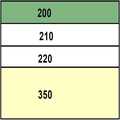
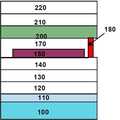
도 2와 같이, 본 발명의 터치 스크린 일체형 유기 발광 표시 장치는 필름 기판(100)과, 상기 필름 기판(100) 상에 차례로 형성된 제 1 에치 스토퍼층(120) 및 제 1 버퍼층(130)과, 상기 제 1 버퍼층(130) 상에 매트릭스 상으로 화소가 정의되며 각 화소별로 박막 트랜지스터를 갖는 박막 트랜지스터 어레이(140)와, 상기 각 화소의 박막 트랜지스터와 접속된 유기 발광 다이오드(150)와, 상기 박막 트랜지스터 어레이(140) 및 유기 발광 다이오드를 덮는 보호층(170)과, 상기 보호층(170)과 접한 터치 전극층(200)과, 상기 터치 전극층(200) 상에 차례로 형성된 제 2 버퍼층(210) 및 제 2 에치 스토퍼층(220) 및 상기 제 2 에치 스토퍼층(220) 상에 형성된 편광판(230)을 포함하여 이루어진다.2, the touch screen integrated type organic light emitting diode display of the present invention includes a
이러한 본 발명의 터치 스크린 일체형 유기 발광 표시 장치에 있어서는, 약 0.7mm 정도로 표시 장치에서 가장 큰 두께를 갖는 글래스 기판의 사용을 완성된 장치에서 생략하여 박막화가 가능하고, 박막 트랜지스터 어레이(140), 유기 발광 다이오드(150) 및 터치 전극층(200) 등을 지지하는 기능을 갖는 기판으로서 플라스틱 절연성 필름인 필름 기판(100)을 이용함으로써, 휘거나 구부릴 수 있는 유연성 있는 표시 장치 구현이 가능하다.In the touch screen integrated type organic light emitting diode display of the present invention, a glass substrate having a maximum thickness of about 0.7 mm can be used as a thin film transistor by omitting the use of the completed device, and the thin
또한, 박막 트랜지스터 어레이(140), 유기 발광 다이오드(150) 및 터치 전극층(200) 등의 어레이 형성 공정시에는 바로 필름 기판 상에 형성시 증착, 패터닝 등을 위한 장비에서 가해지는 열 등의 조건에서 기판이 말려 공정이 정상적으로 이루어질 수 없으므로, 이를 방지하기 위해 상기 박막 트랜지스터 어레이(140) 형성 전과 터치 전극층(200) 형성 전 그 하부에 각각 버퍼층(130, 210)과 에치 스토퍼층(120, 220)을 글래스 기판 상에 형성한 후, 실질적으로 어레이 형성은 글래스 기판을 증착 또는 패터닝 장비로 로딩하여 이루어진다.In the array forming process of the thin
여기서, 상기 제 1, 제 2 에치 스토퍼층(120, 220)은 어레이 형성 후 이후의 글래스 기판의 제거 공정시 상부로 글래스 기판 제거를 위한 식각액이나 레이저 조사로 인한 데미지를 방지하기 위해 구비된다. 그리고, 상기 제 1 에치 스토퍼층(120) 및 제 2 에치 스토퍼층(220)은 예를 들어, 폴리 이미드(polyimide) 또는 포토 아크릴(photo acryl) 등일 수 있다.Here, the first and second
상기 제 1, 제 2 에치 스토퍼층(120, 220)은 대략 1㎛ 내지 10㎛의 범위의 두께로 형성한다.The first and second
그리고, 상기 제 1 버퍼층(130) 및 제 2 버퍼층(210)은 유기 발광 다이오드에 구비된 유기막들에 산소나 수분 침투가 일어남을 방지하기 위해 구비된 것으로, 일종의 하부에서 들어오는 외기 또는 수분의 배리어 기능을 하는 것이다.The
그리고, 상기 제 1 버퍼층(130) 및 제 2 버퍼층(210)은 복수층의 무기막으로 형성한다. 예를 들어, 상기 복수층의 무기막은 SiNx 또는 SiO2의 연속 적층 또는 교번 적층으로 이루어질 수 있다. 실험상 상기 제 1, 제 2 버퍼층(130, 210)으로서 2층 이상으로 약 5000 Å 내지 6500Å 의 두께로 적층시 외기 또는 수분의 침투가 방지됨을 확인할 수 있었다. 상기 제 1, 제 2 버퍼층(130, 210)의 각각의 총 두께는 1㎛ 이하로 하여 터치 스크린 일체형 표시 장치의 두께를 늘리지 않도록 한다.The
상기 터치 전극층(200)은 서로 교차하는 형상의 제 1 터치 전극(미도시) 및 제 2 터치 전극(미도시)과, 상기 제 1 및 제 2 터치 전극에 각각 신호를 전달하는 터치 패드 전극(미도시)을 포함한다. 상기 터치 패드 전극은 상기 박막 트랜지스터 어레이에 형성되는 더미 금속과 접속될 수 있다. 도면 상에는 상기 더미 금속을 포함하도록 박막 트랜지스터 어레이가 층상으로 도시되어 있고, 상기 터치 패드 전극, 제 1, 제 2 터치 전극을 포함하도록 하여 하나의 층상으로 터치 전극층이 도시되어 있으나, 이들 층은 각 전극별로 나누어 패터닝되어 있다.The
여기서, 상기 제 1, 제 2 터치 전극은 투명 전극으로 이루어지며, 상기 패드 전극은 전도율이 좋은 차광성의 금속으로 이루어질 수 있다. 그리고, 제 1, 제 2 터치 전극은 동일층에 위치할 수도 있고, 서로 다른 층에 위치할 수 있다. 예를 들어, 상기 제 1, 제 2 터치 전극이 동일층이 있을 경우, 제 1, 제 2 터치 전극의 교차부에서는 다른 층에 인접한 제 1 터치 전극간 또는 제 2 터치 전극간 콘택된 별도의 연결패턴을 두어 제 1, 제 2 터치 전극간 쇼트됨을 방지한다.Here, the first and second touch electrodes may be transparent electrodes, and the pad electrode may be formed of a light-shielding metal having a high conductivity. The first and second touch electrodes may be located on the same layer or on different layers. For example, when the first and second touch electrodes are on the same layer, a separate connection is made between the first touch electrodes adjacent to the other layer or between the second touch electrodes at the intersections of the first and second touch electrodes Thereby preventing a short circuit between the first and second touch electrodes.
상기 박막 트랜지스터 어레이는 화소 영역을 정의하며 서로 교차하는 게이트 라인과 데이터 라인과, 상기 게이트 라인과 데이터 라인의 교차부에 형성된 박막 트랜지스터를 포함하는 데, 이러한 화소 영역들이 매트릭스 상으로 배치된다. 상기 더미 금속은 상기 화소 영역 외곽의 OLED 패드부측에 게이트 라인 또는 데이터 라인을 이루는 금속과 동일층에 형성하는 것이다.The thin film transistor array includes a gate line and a data line which define a pixel region and intersect with each other, and a thin film transistor formed at an intersection of the gate line and the data line. The pixel regions are arranged in a matrix. The dummy metal is formed on the same layer as the metal forming the gate line or the data line on the side of the OLED pad outside the pixel region.
그리고, 상기 터치 패드 전극은 터치 전극층 가장 자리에 위치하는 것으로, 터치 패드 전극과 상기 더미 금속이 상하에서 서로 대응위치에 형성되어 금속 도전성 볼(180)을 포함한 씰재에 의해 접속되는 것이다.The touch pad electrode is located at the edge of the touch electrode layer, and the touch pad electrode and the dummy metal are formed at corresponding positions on the upper and lower sides and are connected by the sealing material including the metal
여기서, 상기 금속 도전성 볼은 Au 또는 Ag를 포함한 것일 수 있다.Here, the metal conductive ball may include Au or Ag.
상기 편광판(230)은 상기 제 2 에치 스토퍼층(220) 측의 글래스 기판 제거 후 노출된 표면에 부착되는 것으로, 별도의 접착층(미도시)을 개재하여 부착될 수 있거나 혹은 상기 편광판(230)의 대응면이 접착면을 가질 경우, 접착층을 생략하여 바로 상기 제 2 에치 스토퍼층(220)과 접하여 형성될 수 있다.The
이 경우, 상기 편광판(230)은 상기 터치 전극층(200)을 덮도록 그 상부에 위치함으로써, 외부에서 바라볼 때, 편광판(230)으로 터치 전극층(200)이 가려져 터치 전극층(200) 내부의 전극 패턴이 시인되는 현상을 방지할 수 있다.In this case, the
또한, 상기 필름 기판(100)은 상기 제 1 에치 스토퍼층(120) 측의 글래스 기판 제거 후 노출된 표면에 부착되며, 도시된 바와 같이, 접착층(110)을 개재하여 이격없이 상기 제 1 에치 스토퍼층(120) 배면에 형성될 수 있다.The
여기서, 상기 필름 기판(100)은 터치 스크린 일체형 유기 발광 표시 장치가 충분히 휘거나 구부러질 정도로 200㎛ 이하의 두께로 마련한다.Here, the
한편, 상기 박막 트랜지스터 어레이(140)과 유기 발광 다이오드(150)를 덮는 보호층(170)은 상기 박막 트랜지스터 어레이(140)의 패드부를 오픈하여 형성한다.The
상기 유기 발광 다이오드(150)는 서로 대향되는 제 1 전극과 제 2 전극 및 제 1, 제 2 전극 사이에 발광층을 포함하며, 경우에 따라, 각 전극과 발광층 사이에 유기물 성분의 공통층이 더 포함될 수 있다. 이 때, 상기 제 1 전극은 상기 박막 트랜지스터와 접속되며, 상기 제 2 전극은 상기 패드부측으로 신호를 인가받을 수 있다.The organic
이하, 도면을 참조하여 본 발명의 터치 스크린 일체형 유기 발광 표시 장치의 제조 방법에 대해 설명한다.Hereinafter, a method of manufacturing the touch screen integrated type organic light emitting diode display of the present invention will be described with reference to the drawings.
도 3a 내지 도 3e는 본 발명의 터치 스크린 일체형 유기 발광 표시 장치의 제조 방법을 나타낸 공정 단면도이다.FIGS. 3A to 3E are cross-sectional views illustrating a method of manufacturing a touch screen integrated type organic light emitting display according to the present invention.
이하의 설명에서, 각 층의 성분 및 두께는 상술한 터치 스크린 일체형 유기 발광 표시 장치와 동일하므로 생략한다.In the following description, the components and the thickness of each layer are the same as those of the above-described touch screen integrated type organic light emitting display device, and therefore, they are omitted.
도 3a와 같이, 본 발명의 터치 스크린 일체형 유기 발광 표시 장치는, 먼저 제 1 기판(300) 상에 제 1 에치 스토퍼층(120) 및 제 1 버퍼층(130)과, 상기 제 1 버퍼층(130) 상에 매트릭스 상으로 화소가 정의되며 각 화소별로 박막 트랜지스터를 갖는 박막 트랜지스터 어레이(140) 및 상기 각 화소의 박막 트랜지스터와 접속된 유기 발광 다이오드(150), 상기 박막 트랜지스터 어레이(130) 및 유기 발광 다이오드(150)를 덮는 보호층(170)을 차례로 형성한다.3A, the touch screen integrated organic light emitting diode display of the present invention includes a
여기서, 상기 제 1 기판(300)은 글래스 기판으로 박막 트랜지스터 어레이(130) 및 유기 발광 다이오드(150) 형성시 진입되는 증착 또는 패터닝 장비에서 패턴이 정확한 위치에 형성되도록 제 1 에치 스토퍼층(120) 및 제 1 버퍼층(130)이 휘거나 말리지 않고 지지하는 기능을 담당한다.Here, the
한편, 상기 박막 트랜지스터 어레이 형성시 상기 제 1 버퍼층(130)에 가장자리에 상당한 패드부에 더미 금속(미도시)를 더 형성한다.On the other hand, a dummy metal (not shown) is further formed on the pad portion corresponding to the edge of the
이어, 도 3b와 같이, 글래스 성분의 제 2 기판(350) 상에 제 2 에치 스토퍼층(220) 및 제 2 버퍼층(210)과, 상기 제 2 버퍼층(210) 상에 터치 전극층(200)을 차례로 형성한다. 여기서, 상기 터치 전극층(200)은 상기 제 2 버퍼층 상에, 서로 교차하는 형상의 제 1 터치 전극 및 제 2 터치 전극과, 상기 제 1 및 제 2 터치 전극에 각각 신호를 전달하는 터치 패드 전극을 포함할 수 있다. 경우에 따라, 상기 제 1 터치 전극과 제 2 터치 전극을 서로 다른 층에 형성할 경우 층간에 절연막을 더 구비할 수 있다.3B, a second
한편, 상기 제 1, 제 2 버퍼층(130, 210)은 각각 산화막(SiO2) 또는 질화막(SiNx)을 연속 적층 또는 교번 적층하여 이루어진다. 상기 제 1, 제 2 버퍼층(130, 210)은, 상기 제 1 기판(300) 상에 상기 제 2 기판(350)을 합착하는 이후의 공정에서 상기 유기 발광 다이오드(150)로 수분이나 외기가 투습됨을 방지하는 배리어로 기능하게 한다.Meanwhile, the first and second buffer layers 130 and 210 are formed by successively stacking or alternately stacking an oxide film (SiO2) or a nitride film (SiNx). The first and second buffer layers 130 and 210 are formed on the
그리고, 공정 도면에는 일부분만을 도시하여 상기 제 1 기판(300)과 제 2 기판(350)이 동일 크기로 도시되어 있으나, 실제 상기 제 1 기판(300)이 상기 제 2 기판(350)보다 외측으로 더 돌출되어 있는 크기이다. 그리고, 제 1 기판(300)이 돌출된 부분에는 구동 IC와 이와 전기적으로 연결된 플렉서블 인쇄회로 기판이 이후의 회로 실장에서 접속된다(도 4 및 도 5 참조).Although the
이어, 도 3c와 같이, 상기 터치 전극층(200)을 상기 보호층(170)에 대면하여 부착하며, 동시에 상기 더미 금속 또는 상기 터치 패드 전극에 금속 도전성 볼(180)을 포함한 씰재를 형성하여, 상기 더미 금속과 상기 터치 패드 전극이 서로 본딩 접속되도록 한다. 한편, 상기 터치 전극층(200)을 상기 보호층(170)에 대면 부착시 상기 보호층(170)이 갖는 접착성을 이용할 수도 있고, 별도의 접착층 또는 접착재를 더 개재하여 부착이 이루어질 수도 있다.3 (c), the
이어, 도 3d와 같이, 식각 또는 레이저 조사에 의해 상기 제 1 기판(300)을 제거한 후, 노출된 제 1 에치 스토퍼층(120)의 배면에 필름 기판(100)을 부착한다. 이 경우, 상기 필름 기판(100)과 상기 제 1 에치 스토퍼층(120) 사이에 접착층(110)을 더 개재할 수 있다.Next, as shown in FIG. 3D, the
이어, 도 3e와 같이, 제 1 기판의 제거와 같은 방식으로 상기 제 1 기판(350)을 제거한다.Next, as shown in FIG. 3E, the
그리고, 도 2와 같이 노출된 제 2 에치 스토퍼층(220)의 배면에 편광판(230)을 부착한다.Then, the
경우에 따라, 상기 도 3d와 공정까지 마친 후, 상기 제 2 기판(350)을 제거하지 않고 유지하거나 일부 두께 남겨 이를 커버 윈도우(cover window)로 이용할 수도 있다. 이 경우에는 상기 제 2 기판(350) 상에 편광판을 더 형성할 수 있다.If necessary, the
이하, 도면을 참조하여 구체적으로 터치 전극층 및 박막 트랜지스터 어레이 또는 유기 발광 다이오드의 회로부 실장을 참조한다.Hereinafter, the touch electrode layer and the thin film transistor array or the circuit portion mounting of the organic light emitting diode will be concretely described with reference to the drawings.
도 4는 본 발명의 터치 스크린 일체형 유기 발광 표시 장치의 회로부 실장을 나타낸 단면도이며, 도 5는 도 4의 평면도이다.FIG. 4 is a cross-sectional view of a circuit portion of a touch screen integrated type organic light emitting diode display according to the present invention, and FIG. 5 is a plan view of FIG.
도 4 및 도 5와 같이, 터치 전극층(200) 및 박막 트랜지스터 어레이(140) 또는 유기 발광 다이오드(150)의 구동회로 구비를 위해 상기 제 1 버퍼층(130), 제 1 에치 스토퍼층(120) 및 필름 기판(100)은 상기 터치 전극층(200)보다 외측으로 돌출된다.4 and 5, the
그리고, 상기 제 1 버퍼층(130)의 상기 터치 전극층(200)보다 돌출된 외측에 상기 제 1 터치 전극 및 제 2 터치 전극과 신호를 주고 받는 터치 구동 IC(400)와, 상기 박막 트랜지스터 어레이 및 상기 유기 발광 다이오드에 신호를 전달하는 OLED IC(400)를 갖는다. 도시된 도면은 터치 구동 IC와 OLED IC가 하나의 IC로 집적화하여 형성된 것을 나타낸 것으로, 경우에 따라 별개의 IC로 나누어 형성할 수도 있다.A
이와 같이, 상기 터치 구동 IC를 상기 제 1 버퍼층(130) 상에 구비할 경우, 터치 전극층에서 구동 IC 및 회로 실장을 생략할 수 있어, 터치 전극층 구성을 간소화할 수 있으며, 회로 기판을 하나 생략할 수 있어, 모듈 공정이 간소화된다.In this way, when the touch-driving IC is provided on the
여기서, 상기 터치 구동 IC와 OLED IC(400)은, 상기 제 1 버퍼층(130)의 상기 터치 전극층(200)보다 돌출된 외측 가장자리에 형성된 플렉서블 인쇄회로 기판(FPCB)(550)과 연결된다.The touch driver IC and the
한편, 상기 편광판(230) 상에 커버 윈도우(500)를 터치면 보호를 위해 접착층(450)을 더 개재하여 형성할 수 있다. 이 경우, 상기 커버 윈도우는 절연성 투명 필름으로 형성하여, 전체 터치 스크린 일체형 유기 발광 표시 장치의 총 두께를 늘리지 않도록 하는 것이 보다 바람직할 수 있다. 상기 커버 윈도우는 생략할 수도 있다. 그 경우에는, 상기 편광판(230)이 터치면의 보호 기능을 담당할 수 있다. 그리고, 보호 기능을 위해 상기 편광판(230)의 두께를 조절하거나 외부광 난반사를 방지하기 위해 편광 기능 외의 별도의 광학층을 더 편광판(230) 내에 더 포함할 수도 있다.On the other hand, the cover window 500 may be formed on the
도시된 바와 같이, 상기 제 1 버퍼층(130), 상기 제 1 에치 스토퍼층(120) 및 상기 필름 기판(100)은 동일한 제 1 크기이며, 상기 터치 전극층(200), 상기 제 2 버퍼층(210) 및 제 2 에치 스토퍼층(220)은 동일한 제 2 크기이며, 상기 제 1 크기가 제 2 크기보다 크다.The
한편, 설명하지 않은 도면 부호 420은 상기 플렉서블 인쇄 회로 기판(550)과 상기 터치 구동 IC와 OLED IC(400)와의 연결을 위한 접속부로, 상기 제 1 버퍼층(130) 상에 상기 박막 트랜지스터 어레이에 패드 전극 및 이와 연결된 배선이 형성되어, 상기 터치 구동 IC와 OLED IC(400)의 전기적 연결이 이루어진다.A
그리고, 설명하지 않은 도면 부호 600은 상기 플렉서블 인쇄 회로 기판(550) 상에 형성되는 제어부로 상기 터치 구동 IC 및 OLED IC(400)로 전달하는 신호를 생성하고 터치 구동 IC 및 OLED IC(400)로부터 센싱되는 신호를 저장/분석한다.An
그리고, 상기 플렉서블 인쇄회로 기판(550)은 상기 필름 기판(100)의 하부면으로 접혀져 부착될 수 있다.The flexible printed
한편, 상기 점선 영역은 터치 센싱 영역이나 표시 영역으로 박막 트랜지스터 어레이의 화소들을 매트릭스 상으로 상기 점선 영역 내에 위치하며, 패드부는 그 외측에 정의된다.On the other hand, the dotted line area is defined as a touch sensing area or a display area, and the pixels of the thin film transistor array are positioned in the dotted line area in a matrix form, and the pad part is defined on the outside thereof.
이상에서 설명한 본 발명은 상술한 실시 예 및 첨부된 도면에 한정되는 것이 아니고, 본 발명의 기술적 사상을 벗어나지 않는 범위 내에서 여러 가지 치환, 변형 및 변경이 가능하다는 것이 본 발명이 속하는 기술분야에서 종래의 지식을 가진 자에게 있어 명백할 것이다.It will be apparent to those skilled in the art that various modifications and variations can be made in the present invention without departing from the spirit or scope of the invention. Will be clear to those who have knowledge of.
100: 필름 기판 110: 접착층
120: 제 1 에치 스토퍼층 130: 제 1 버퍼층
140: 박막 트랜지스터 어레이 150: 유기 발광 다이오드
170: 보호층 180: 금속 도전성 볼
200: 터치 전극층 210: 제 2 버퍼층
220: 제 2 에치 스토퍼층 230: 편광판
300: 제 1 기판 350: 제 2 기판
400: 터치 구동 IC 및 OLED IC 450: 접착층
500: 커버 윈도우 550: 플렉서블 인쇄 회로 기판
600: 제어부100: film substrate 110: adhesive layer
120: first etch stopper layer 130: first buffer layer
140: thin film transistor array 150: organic light emitting diode
170: protective layer 180: metal conductive ball
200: touch electrode layer 210: second buffer layer
220: second etch stopper layer 230: polarizer
300: first substrate 350: second substrate
400: Touch-driving IC and OLED IC 450: Adhesive layer
500: Cover window 550: Flexible printed circuit board
600:
Claims (27)
Translated fromKorean상기 필름 기판 상에, 차례로 상기 제 1 크기로 형성된 제 1 에치 스토퍼층 및 제 1 버퍼층;
상기 제 1 버퍼층 상에 매트릭스 상으로 화소들이 정의되며 상기 화소들 외측 일부에 패드부를 갖고, 각 화소별로 박막 트랜지스터를 갖는 박막 트랜지스터 어레이;
상기 박막 트랜지스터 어레이와 동일층으로 상기 제 1 버퍼층 상에, 상기 상기 화소들 외측에 위치한 더미 금속;
상기 각 화소의 박막 트랜지스터와 접속된 유기 발광 다이오드;
상기 유기 발광 다이오드를 덮고, 상기 더미 금속을 노출시키는 보호층;
상기 보호층보다는 크며, 상기 제 1 크기보다 작은 제 2 크기로 구비되고, 상기 보호층과 접하며 서로 교차하는 형상의 제 1 터치 전극 및 제 2 터치 전극과, 상기 더미 금속에 대응하여 위치하고 상기 제 1 및 제 2 터치 전극에 각각 신호를 전달하는 터치 패드 전극을 포함한 터치 전극층;
금속 도전성 볼을 포함하며, 상기 보호층 외측에서 상기 터치 패드 전극과 상기 더미 금속을 접속하는 씰재;
상기 터치 전극층 상에 차례로, 상기 제 2 크기로 상기 보호층 및 터치 패드 전극을 중첩하되 상기 패드부를 노출시키도록 형성된 제 2 버퍼층 및 제 2 에치 스토퍼층; 및
상기 제 2 에치 스토퍼층 상에 형성된 편광판을 포함하여 이루어진 것을 특징으로 하는 터치 스크린 일체형 유기 발광 표시 장치.A film substrate of a first size;
A first etch stopper layer and a first buffer layer sequentially formed on the film substrate at the first size;
A thin film transistor array in which pixels are defined in a matrix form on the first buffer layer and pad portions are formed in an outer portion of the pixels and thin film transistors are provided for each pixel;
A dummy metal located on the first buffer layer in the same layer as the thin film transistor array, the dummy metal being located outside the pixels;
An organic light emitting diode connected to the thin film transistor of each pixel;
A protective layer covering the organic light emitting diode and exposing the dummy metal;
A first touch electrode and a second touch electrode having a size larger than the protection layer and having a second size smaller than the first size and in contact with the protection layer and intersecting with each other, A touch electrode layer including a touch pad electrode for transmitting a signal to the second touch electrode;
A sealing material including a metal conductive ball and connecting the touch pad electrode and the dummy metal outside the protective layer;
A second buffer layer and a second etch stopper layer formed on the touch electrode layer in order to expose the pad portion while overlapping the protective layer and the touch pad electrode in the second size; And
And a polarizer formed on the second etch stopper layer.
상기 필름 기판은 플라스틱 절연성 필름인 것을 특징으로 하는 터치 스크린 일체형 유기 발광 표시 장치.The method according to claim 1,
Wherein the film substrate is a plastic insulating film.
상기 제 1 에치 스토퍼층 및 제 2 에치 스토퍼층은 폴리 이미드 또는 포토 아크릴인 것을 특징으로 하는 터치 스크린 일체형 유기 발광 표시 장치.The method according to claim 1,
Wherein the first etch stopper layer and the second etch stopper layer are polyimide or photoacid.
상기 제 1 버퍼층 및 제 2 버퍼층은 복수층의 무기막으로 이루어진 것을 특징으로 하는 터치 스크린 일체형 유기 발광 표시 장치.The method according to claim 1,
Wherein the first buffer layer and the second buffer layer are made of a plurality of inorganic films.
상기 복수층의 무기막은 SiNx 또는 SiO2의 연속 적층 또는 교번 적층으로 이루어지는 것을 특징으로 하는 터치 스크린 일체형 유기 발광 표시 장치.5. The method of claim 4,
Wherein the plurality of inorganic films are formed of a continuous lamination or an alternate lamination of SiNx or SiO2.
상기 금속 도전성 볼은 Au 또는 Ag를 포함한 것을 특징으로 하는 터치 스크린 일체형 유기 발광 표시 장치.
The method according to claim 1,
Wherein the metal conductive ball comprises Au or Ag.
상기 제 1 버퍼층의 상기 터치 전극층보다 돌출된 외측에 상기 제 1 터치 전극 및 제 2 터치 전극과 신호를 주고 받는 터치 구동 IC와, 상기 박막 트랜지스터 어레이 및 상기 유기 발광 다이오드에 신호를 전달하는 OLED IC를 갖는 것을 특징으로 하는 터치 스크린 일체형 유기 발광 표시 장치.The method according to claim 1,
A touch driving IC for transmitting and receiving signals to and from the first touch electrode and the second touch electrode on an outer side of the first buffer layer protruding from the touch electrode layer, and an OLED IC for transmitting a signal to the thin film transistor array and the organic light emitting diode Wherein the organic light emitting display device comprises:
상기 터치 구동 IC와 상기 OLED IC은, 상기 제 1 버퍼층의 상기 터치 전극층보다 돌출된 외측 가장자리에 형성된 플렉서블 인쇄회로 기판과 연결된 것을 특징으로 하는 터치 스크린 일체형 유기 발광 표시 장치.12. The method of claim 11,
Wherein the touch driving IC and the OLED IC are connected to a flexible printed circuit board formed on an outer edge of the first buffer layer protruding from the touch electrode layer.
상기 편광판 상에 커버 윈도우를 더 포함하는 것을 특징으로 하는 터치 스크린 일체형 유기 발광 표시 장치.The method according to claim 1,
Further comprising a cover window on the polarizing plate.
상기 커버 윈도우는 절연성 투명 필름인 것을 특징으로 하는 터치 스크린 일체형 유기 발광 표시 장치.14. The method of claim 13,
Wherein the cover window is an insulating transparent film.
상기 제 1 버퍼층 상에 매트릭스 상으로 화소들이 정의되며 각 화소별로 박막 트랜지스터를 갖는 박막 트랜지스터 어레이 및 상기 박막 트랜지스터 어레이와 동일층에, 상기 제 1 버퍼층 상에 형성된 더미 금속 및 상기 화소들 외측 일부에 패드부를 형성하는 단계;
상기 각 화소의 박막 트랜지스터와 접속된 유기 발광 다이오드를 형성하는 단계;
상기 더미 금속을 노출시키며 상기 유기 발광 다이오드를 덮는 보호층을 형성하는 단계;
상기 보호층보다 크며 상기 제 1 기판보다는 작은 제 2 크기로, 제 2 기판을 마련 후, 상기 제 2 기판 상에 상기 제 2 크기로, 제 2 에치 스토퍼층 및 제 2 버퍼층을 차례로 형성하는 단계;
상기 제 2 버퍼층 상에 상기 매트릭스 상의 화소들에 대응하여, 서로 교차하는 형상의 제 1 터치 전극 및 제 2 터치 전극과, 상기 더미 금속에 대응되는 위치에 상기 제 1 및 제 2 터치 전극에 각각 신호를 전달하는 터치 패드 전극을 포함한 터치 전극층을 차례로 형성하는 단계;
상기 제 1 및 제 2 터치 전극을 포함한 터치 전극층을 상기 보호층에 대면하여 부착하고, 상기 보호층 외측에서 상기 터치 패드 전극과 상기 더미 금속 사이에 금속 도전성 볼을 개재하여 접속시키되, 상기 제 2 기판으로부터 상기 제 1 기판의 패드부를 노출시키는 단계;
상기 제 1 기판 및 제 2 기판을 제거하는 단계;
상기 제 1 에치 스토퍼층의 노출된 면에 필름 기판을 부착하는 단계; 및
상기 제 2 에치 스토퍼층의 노출된 면에 편광판을 부착하는 단계를 포함하여 이루어진 것을 특징으로 하는 터치 스크린 일체형 유기 발광 표시 장치의 제조 방법.
Forming a first etch stopper layer and a first buffer layer at the first size on a first substrate having a first size;
A thin film transistor array having pixels arranged in a matrix on the first buffer layer and having thin film transistors for each pixel and a dummy metal layer formed on the first buffer layer and a pad Forming a part;
Forming an organic light emitting diode connected to the thin film transistor of each pixel;
Forming a protective layer that exposes the dummy metal and covers the organic light emitting diode;
Forming a second etch stopper layer and a second buffer layer on the second substrate in the second size with a second size larger than the protective layer and smaller than the first substrate after the second substrate is formed;
A first touch electrode and a second touch electrode on the second buffer layer, the first touch electrode and the second touch electrode intersecting with each other on the matrix, and a signal Forming a touch electrode layer including a touch pad electrode for transmitting a touch signal;
A touch electrode layer including the first and second touch electrodes is attached to the protective layer so as to face each other and a metal conductive ball is interposed between the touch pad electrode and the dummy metal at the outside of the protective layer, Exposing a pad portion of the first substrate;
Removing the first substrate and the second substrate;
Attaching a film substrate to an exposed surface of the first etch stopper layer; And
And attaching a polarizer to the exposed surface of the second etch stopper layer.
상기 제 1 기판 및 제 2 기판을 제거하는 단계는 상기 제 1 기판과 제 2 기판을 식각하거나 레이저를 조사하여 이루어지는 것을 특징으로 하는 터치 스크린 일체형 유기 발광 표시 장치의 제조 방법.17. The method of claim 16,
Wherein the step of removing the first substrate and the second substrate comprises etching the first substrate and the second substrate or irradiating a laser beam thereto.
상기 제 1 버퍼층 및 제 2 버퍼층의 형성은 SiNx 또는 SiO2의 연속 적층 또는 교번 적층하여 이루어지는 것을 특징으로 하는 터치 스크린 일체형 유기 발광 표시 장치의 제조 방법.17. The method of claim 16,
Wherein the first buffer layer and the second buffer layer are formed by successively stacking or alternating layers of SiNx or SiO2.
상기 제 1 기판이 상기 제 2 기판보다 외측으로 더 돌출되어 있는 크기인 것을 특징으로 하는 터치 스크린 일체형 유기 발광 표시 장치의 제조 방법.17. The method of claim 16,
Wherein the first substrate is further protruded outward than the second substrate.
상기 제 1 에치 스토퍼층의 노출된 면에 필름 기판을 부착하는 단계는 상기 제 1 에치 스토퍼층과 상기 필름 기판 사이에 접착층을 개재하여 이루어지는 것을 특징으로 하는 터치 스크린 일체형 유기 발광 표시 장치의 제조 방법.17. The method of claim 16,
Wherein the step of attaching the film substrate to the exposed surface of the first etch stopper layer comprises an adhesive layer interposed between the first etch stopper layer and the film substrate.
상기 제 1 버퍼층의 상기 터치 전극층보다 돌출된 외측에, 상기 제 1 터치 전극 및 제 2 터치 전극과 신호를 주고 받는 터치 구동 IC와, 상기 박막 트랜지스터 어레이 및 상기 유기 발광 다이오드에 신호를 전달하는 OLED IC를 접속시키는 단계를 더 포함하는 것을 특징으로 하는 터치 스크린 일체형 유기 발광 표시 장치의 제조 방법.17. The method of claim 16,
A touch driving IC for transmitting and receiving signals to and from the first touch electrode and the second touch electrode on an outer side of the first buffer layer protruding from the touch electrode layer and an OLED IC for transmitting a signal to the thin film transistor array and the organic light emitting diode The method of claim 1, further comprising the step of:
상기 터치 구동 IC와 상기 OLED IC와 접속되도록, 상기 제 1 버퍼층의 상기 터치 전극층보다 돌출된 외측 가장자리에 플렉서블 인쇄회로 기판을 형성하는 단계를 더 포함하는 것과 특징으로 하는 터치 스크린 일체형 유기 발광 표시 장치의 제조 방법.26. The method of claim 25,
Further comprising the step of forming a flexible printed circuit board on an outer edge of the first buffer layer protruding from the touch electrode layer so as to be connected to the touch driving IC and the OLED IC. Gt;
상기 편광판 상에 커버 윈도우를 형성하는 단계를 더 포함하는 것을 특징으로 하는 터치 스크린 일체형 유기 발광 표시 장치의 제조 방법.17. The method of claim 16,
And forming a cover window on the polarizing plate. The method of any one of the preceding claims, further comprising forming a cover window on the polarizing plate.
Priority Applications (4)
| Application Number | Priority Date | Filing Date | Title |
|---|---|---|---|
| KR1020110130621AKR101908501B1 (en) | 2011-12-07 | 2011-12-07 | Integrated Touch Screen With Organic Emitting Display Device and Method for Manufacturing the Same |
| US13/592,207US8946690B2 (en) | 2011-12-07 | 2012-08-22 | Touch screen integrated organic light emitting display device and method for fabricating the same |
| CN201210303668.4ACN103151467B (en) | 2011-12-07 | 2012-08-23 | Be integrated with organic light-emitting display device and the manufacture method thereof of touch-screen |
| US14/582,684US9196876B2 (en) | 2011-12-07 | 2014-12-24 | Touch screen integrated organic light emitting display device and method for fabricating the same |
Applications Claiming Priority (1)
| Application Number | Priority Date | Filing Date | Title |
|---|---|---|---|
| KR1020110130621AKR101908501B1 (en) | 2011-12-07 | 2011-12-07 | Integrated Touch Screen With Organic Emitting Display Device and Method for Manufacturing the Same |
Publications (2)
| Publication Number | Publication Date |
|---|---|
| KR20130063971A KR20130063971A (en) | 2013-06-17 |
| KR101908501B1true KR101908501B1 (en) | 2018-10-17 |
Family
ID=48549421
Family Applications (1)
| Application Number | Title | Priority Date | Filing Date |
|---|---|---|---|
| KR1020110130621AActiveKR101908501B1 (en) | 2011-12-07 | 2011-12-07 | Integrated Touch Screen With Organic Emitting Display Device and Method for Manufacturing the Same |
Country Status (3)
| Country | Link |
|---|---|
| US (2) | US8946690B2 (en) |
| KR (1) | KR101908501B1 (en) |
| CN (1) | CN103151467B (en) |
Families Citing this family (76)
| Publication number | Priority date | Publication date | Assignee | Title |
|---|---|---|---|---|
| KR101341030B1 (en) | 2012-08-29 | 2013-12-13 | 엘지디스플레이 주식회사 | Organic emitting display device and method for manufacturing the same |
| CN103296491B (en)* | 2012-09-05 | 2016-03-30 | 上海天马微电子有限公司 | Electric connection structure of conductive pad and touch screen with same |
| CN103677357B (en)* | 2012-09-06 | 2016-12-28 | 宸鸿科技(厦门)有限公司 | For the covering plate structure of contact panel and manufacture method thereof and contact panel |
| KR102207861B1 (en)* | 2013-04-26 | 2021-01-26 | 삼성전자주식회사 | Method for displaying and an electronic device thereof |
| US10884551B2 (en)* | 2013-05-16 | 2021-01-05 | Analog Devices, Inc. | Integrated gesture sensor module |
| CN103294271A (en)* | 2013-05-30 | 2013-09-11 | 南昌欧菲光科技有限公司 | Conducting film of touch screen and method for manufacturing conducting film |
| DE102013012110A1 (en)* | 2013-07-12 | 2015-01-15 | e.solutions GmbH | Touch-sensitive screen, in particular for use in a motor vehicle |
| TWI506341B (en)* | 2013-07-18 | 2015-11-01 | Ye Xin Technology Consulting Co Ltd | Touch and display panel |
| KR101443689B1 (en)* | 2013-08-23 | 2014-09-23 | 동우 화인켐 주식회사 | Touch sensing electrode combined with polarization plate |
| KR102091035B1 (en)* | 2013-09-03 | 2020-03-20 | 엘지디스플레이 주식회사 | Display device having touch screen |
| CN103529985A (en)* | 2013-09-24 | 2014-01-22 | 昆山鑫宏达电子科技有限公司 | Improved type touch screen |
| CN105975126A (en)* | 2013-09-29 | 2016-09-28 | 宸鸿科技(厦门)有限公司 | Touch panel and fabrication method therefor |
| CN103560209A (en)* | 2013-10-12 | 2014-02-05 | 深圳市华星光电技术有限公司 | Organic light-emitting diode device and manufacturing method thereof |
| CN104637976B (en)* | 2013-11-12 | 2018-10-19 | 宸鸿光电科技股份有限公司 | organic light emitting diode touch display device |
| KR102192035B1 (en) | 2013-12-02 | 2020-12-17 | 삼성디스플레이 주식회사 | Flexible display device including touch detecting sensor |
| KR102132697B1 (en) | 2013-12-05 | 2020-07-10 | 엘지디스플레이 주식회사 | Curved Display Device |
| CN203689474U (en) | 2013-12-09 | 2014-07-02 | 昆山工研院新型平板显示技术中心有限公司 | Touch control structure of active matrix organic luminous display screen |
| KR102124906B1 (en)* | 2013-12-26 | 2020-07-07 | 엘지디스플레이 주식회사 | Organic electro luminescent device having touch screen and method of fabricationg the same |
| CN104750284B (en)* | 2013-12-27 | 2019-02-19 | 昆山工研院新型平板显示技术中心有限公司 | A touch display device and a manufacturing method thereof |
| US9836165B2 (en) | 2014-05-16 | 2017-12-05 | Apple Inc. | Integrated silicon-OLED display and touch sensor panel |
| CN104111752A (en)* | 2014-06-10 | 2014-10-22 | 深圳市鹏达源电子科技有限公司 | Touch display module and touch screen with touch display module used |
| CN104091559B (en)* | 2014-06-19 | 2016-09-14 | 京东方科技集团股份有限公司 | Image element circuit and driving method, display device |
| KR102173545B1 (en)* | 2014-08-05 | 2020-11-04 | 엘지디스플레이 주식회사 | Organic light emitting display device having touch structure of in-cell type |
| US9927939B2 (en) | 2014-08-13 | 2018-03-27 | Samsung Display Co., Ltd. | Touch panel and display apparatus including the same |
| KR102276997B1 (en) | 2014-10-13 | 2021-07-14 | 삼성디스플레이 주식회사 | Display device with touch sensor |
| CN105589585A (en)* | 2014-10-21 | 2016-05-18 | 宸鸿科技(厦门)有限公司 | Touch device and production method thereof |
| KR102296733B1 (en)* | 2014-11-06 | 2021-09-01 | 삼성디스플레이 주식회사 | Organic light emitting device |
| US9590129B2 (en) | 2014-11-19 | 2017-03-07 | Analog Devices Global | Optical sensor module |
| KR101758438B1 (en)* | 2014-12-02 | 2017-07-17 | 삼성에스디아이 주식회사 | Composition for window film, flexible window film prepared using the same and flexible display apparatus comprising the same |
| KR101835866B1 (en) | 2014-12-17 | 2018-03-08 | 삼성에스디아이 주식회사 | Composition for window film, flexible window film prepared using the same and flexible display apparatus comprising the same |
| US9535522B2 (en)* | 2014-12-22 | 2017-01-03 | Lg Display Co., Ltd. | Flexible organic light emitting diode display device |
| US9490312B2 (en)* | 2014-12-22 | 2016-11-08 | Lg Display Co., Ltd. | Organic light emitting diode display device with flexible printed circuit film |
| KR101835867B1 (en) | 2014-12-23 | 2018-03-08 | 삼성에스디아이 주식회사 | Composition for window film, flexible window film prepared using the same and flexible display apparatus comprising the same |
| CN104536197A (en)* | 2015-01-22 | 2015-04-22 | 京东方科技集团股份有限公司 | Colored film substrate, array substrate and display device |
| KR102362188B1 (en) | 2015-01-28 | 2022-02-11 | 삼성디스플레이 주식회사 | Organic Light Emitting Device and Method of manufacturing the same |
| KR102369089B1 (en)* | 2015-04-17 | 2022-03-02 | 삼성디스플레이 주식회사 | Flexible display device |
| KR102367990B1 (en)* | 2015-06-15 | 2022-02-28 | 삼성디스플레이 주식회사 | Flat display apparatus and method of manufacturing the same |
| EP3316307A4 (en)* | 2015-06-25 | 2019-02-20 | Shenzhen Royole Technologies Co., Ltd. | METHOD FOR MANUFACTURING TOUCH SCREEN DISPLAY DEVICE |
| KR102490624B1 (en)* | 2015-10-30 | 2023-01-20 | 엘지디스플레이 주식회사 | Flexible Display and Method for Manufacturing the Same |
| KR102419688B1 (en)* | 2015-12-11 | 2022-07-13 | 삼성디스플레이 주식회사 | Display device and manufacturing method of the same |
| KR102457246B1 (en)* | 2016-01-12 | 2022-10-21 | 삼성디스플레이 주식회사 | Display device and method of manufacturing the same |
| CN105489634B (en)* | 2016-02-19 | 2019-08-30 | 上海天马微电子有限公司 | Display panel, manufacturing method thereof and display device |
| KR102562627B1 (en) | 2016-03-21 | 2023-08-03 | 삼성디스플레이 주식회사 | Display device |
| JP6486859B2 (en)* | 2016-03-29 | 2019-03-20 | 日東電工株式会社 | Polarizing film and image display device |
| CN111653583A (en)* | 2016-06-14 | 2020-09-11 | 群创光电股份有限公司 | display device |
| US10541280B1 (en) | 2016-09-16 | 2020-01-21 | Apple Inc. | OLED based touch sensing and user identification |
| KR20180046609A (en)* | 2016-10-28 | 2018-05-09 | 삼성전자주식회사 | Electronic apparatus having a hole area within screen and control method thereof |
| DE102017125366B4 (en)* | 2016-10-31 | 2021-03-18 | Lg Display Co., Ltd. | ORGANIC LIGHT EMITTING DISPLAY DEVICE |
| KR102655241B1 (en) | 2016-11-02 | 2024-04-09 | 삼성디스플레이 주식회사 | Display device |
| KR102593828B1 (en) | 2016-11-02 | 2023-10-26 | 삼성디스플레이 주식회사 | Display device |
| KR102694922B1 (en)* | 2016-11-14 | 2024-08-16 | 삼성디스플레이 주식회사 | Display device |
| KR102311316B1 (en)* | 2017-04-24 | 2021-10-13 | 삼성디스플레이 주식회사 | Display device and fabricating method of the same |
| KR102361262B1 (en)* | 2017-05-30 | 2022-02-09 | 동우 화인켐 주식회사 | Touch sensor integrated with oled and oled display device comprising the same |
| KR102354920B1 (en) | 2017-06-30 | 2022-01-21 | 엘지디스플레이 주식회사 | Display device with integrated touch screen and its manufacturing method |
| KR102329084B1 (en)* | 2017-06-30 | 2021-11-18 | 엘지디스플레이 주식회사 | Touch screen panel and display apparatus with integrated touch screen |
| CN107359182B (en)* | 2017-07-25 | 2020-03-17 | 武汉华星光电半导体显示技术有限公司 | Manufacturing method of OLED display screen integrated with touch function |
| KR102326221B1 (en)* | 2017-07-31 | 2021-11-12 | 엘지디스플레이 주식회사 | DISPLAY DEVICE and METHOD FOR MANUFACTURING THE SAME |
| CN111032814B (en)* | 2017-10-19 | 2022-06-28 | 美国陶氏有机硅公司 | Pressure-sensitive adhesive composition, method for making the same, and use in flexible organic light-emitting diode applications |
| CN107731875B (en)* | 2017-10-19 | 2020-06-19 | 北京翌光科技有限公司 | OLED panel capable of realizing touch function and touch system |
| TWI644126B (en)* | 2017-11-28 | 2018-12-11 | 沅聖科技股份有限公司 | Head mounted display and image device |
| KR102423593B1 (en)* | 2017-12-28 | 2022-07-21 | 엘지디스플레이 주식회사 | Display device and method for manufacturing display device |
| US10712197B2 (en) | 2018-01-11 | 2020-07-14 | Analog Devices Global Unlimited Company | Optical sensor package |
| CN108459773A (en)* | 2018-04-10 | 2018-08-28 | 江苏聚泰科技有限公司 | A kind of display device of novel liquid crystal touch screen |
| GB2575284B (en)* | 2018-07-04 | 2022-04-06 | Flexenable Ltd | Flexible optoelectronic devices |
| CN109032410A (en)* | 2018-07-26 | 2018-12-18 | 京东方科技集团股份有限公司 | Touch-control display panel and preparation method thereof, electronic equipment |
| CN109148722B (en)* | 2018-08-28 | 2020-05-08 | 京东方科技集团股份有限公司 | Organic light-emitting display panel, manufacturing method thereof and display device |
| KR102589499B1 (en)* | 2018-10-31 | 2023-10-13 | 엘지디스플레이 주식회사 | Flexible display apparatus and electronic device comprising the same |
| KR102766477B1 (en) | 2019-01-30 | 2025-02-13 | 삼성디스플레이 주식회사 | Display device |
| KR102769277B1 (en)* | 2019-02-13 | 2025-02-21 | 삼성디스플레이 주식회사 | Display device and manufacturing method thereof |
| KR102819834B1 (en) | 2019-02-21 | 2025-06-13 | 삼성디스플레이 주식회사 | Display device |
| CN109992163B (en)* | 2019-04-15 | 2023-01-03 | 业成科技(成都)有限公司 | Touch sensing module, manufacturing method thereof and electronic device applying touch sensing module |
| KR102170368B1 (en)* | 2019-04-23 | 2020-10-27 | 엘지디스플레이 주식회사 | Organic light emitting display device having touch structure of in-cell type |
| WO2020231452A1 (en)* | 2019-05-10 | 2020-11-19 | Google Llc | Pre-fabricated sensor assembly for interactive objects |
| CN110930879B (en)* | 2019-11-25 | 2020-11-10 | 武汉华星光电半导体显示技术有限公司 | Display device |
| KR20220014626A (en)* | 2020-07-29 | 2022-02-07 | 엘지디스플레이 주식회사 | Flexible display device |
| JP2022076893A (en)* | 2020-11-10 | 2022-05-20 | 日東電工株式会社 | Image display device and its manufacturing method |
Family Cites Families (36)
| Publication number | Priority date | Publication date | Assignee | Title |
|---|---|---|---|---|
| US6879319B2 (en)* | 2002-10-25 | 2005-04-12 | Eastman Kodak Company | Integrated OLED display and touch screen |
| JPWO2004068446A1 (en)* | 2003-01-27 | 2006-05-25 | 東芝松下ディスプレイテクノロジー株式会社 | Manufacturing method of organic EL display |
| KR100746330B1 (en)* | 2005-11-24 | 2007-08-03 | 한국과학기술원 | Connection method between electronic parts using ultrasonic wave |
| KR100732849B1 (en)* | 2005-12-21 | 2007-06-27 | 삼성에스디아이 주식회사 | Organic light emitting display |
| US8144115B2 (en)* | 2006-03-17 | 2012-03-27 | Konicek Jeffrey C | Flat panel display screen operable for touch position determination system and methods |
| US20080079697A1 (en)* | 2006-08-01 | 2008-04-03 | Dong-Ju Lee | Display device and manufacturing method thereof |
| KR101330697B1 (en)* | 2006-12-21 | 2013-11-18 | 삼성디스플레이 주식회사 | Display device |
| KR100829753B1 (en)* | 2007-03-02 | 2008-05-15 | 삼성에스디아이 주식회사 | Organic light emitting display |
| KR100891384B1 (en)* | 2007-06-14 | 2009-04-02 | 삼성모바일디스플레이주식회사 | Flexible Board Bonding and Detachment |
| KR100949339B1 (en)* | 2008-05-06 | 2010-03-26 | 삼성모바일디스플레이주식회사 | Double sided organic light emitting display device |
| US8629842B2 (en)* | 2008-07-11 | 2014-01-14 | Samsung Display Co., Ltd. | Organic light emitting display device |
| US8058783B2 (en)* | 2008-07-25 | 2011-11-15 | Samsung Mobile Display Co., Ltd. | Organic light emitting diode display for suppressing reflection of external light |
| US8169386B2 (en)* | 2008-08-19 | 2012-05-01 | Samsung Mobile Display Co., Ltd. | Organic light emitting diode display |
| KR20100024710A (en)* | 2008-08-26 | 2010-03-08 | 삼성모바일디스플레이주식회사 | Organic light emitting diode display |
| KR100965258B1 (en)* | 2008-08-27 | 2010-06-22 | 삼성모바일디스플레이주식회사 | Organic light emitting display |
| JP2011252934A (en)* | 2008-09-25 | 2011-12-15 | Sharp Corp | Display device |
| KR101065313B1 (en)* | 2008-11-14 | 2011-09-16 | 삼성모바일디스플레이주식회사 | Organic light emitting display device |
| KR100953656B1 (en)* | 2009-01-09 | 2010-04-20 | 삼성모바일디스플레이주식회사 | Organic light emitting diode display |
| TWI587734B (en)* | 2009-03-26 | 2017-06-11 | 精工愛普生股份有限公司 | Organic EL device, method of manufacturing organic EL device, and electronic device |
| KR101323434B1 (en)* | 2009-06-08 | 2013-10-29 | 엘지디스플레이 주식회사 | Organic Light Emitting Display Device |
| CN102033643B (en)* | 2009-09-30 | 2013-03-06 | 北京京东方光电科技有限公司 | Touch screen and manufacturing method thereof |
| KR20110037337A (en)* | 2009-10-06 | 2011-04-13 | 엘지디스플레이 주식회사 | Organic light emitting display device and manufacturing method thereof |
| KR101113538B1 (en)* | 2009-11-03 | 2012-03-02 | 삼성모바일디스플레이주식회사 | Flat Panel Display with a Built-in Touch Screen and Driving Method Thereof |
| KR101309862B1 (en)* | 2009-12-10 | 2013-09-16 | 엘지디스플레이 주식회사 | Liquid Crystal Display Device Including Touch Panel |
| KR101030029B1 (en)* | 2010-01-06 | 2011-04-20 | 삼성모바일디스플레이주식회사 | Organic light emitting display device and manufacturing method thereof |
| KR101142566B1 (en)* | 2010-06-01 | 2012-05-03 | 삼성모바일디스플레이주식회사 | Touch Screen Panel and Display Device Having the Same |
| KR101319347B1 (en)* | 2010-06-10 | 2013-10-16 | 엘지디스플레이 주식회사 | Liquid Crystal Display Panel Associated with Touch Panel |
| KR101735386B1 (en)* | 2010-06-25 | 2017-05-30 | 엘지디스플레이 주식회사 | Liquid crystal display device having touch sensor embedded therein, method for driving the same and method for fabricating the same |
| KR101756656B1 (en)* | 2010-06-25 | 2017-07-11 | 엘지디스플레이 주식회사 | Organic light emitting diode display device including touch panel |
| KR20120004862A (en)* | 2010-07-07 | 2012-01-13 | 삼성모바일디스플레이주식회사 | Organic light emitting display |
| KR101740646B1 (en)* | 2010-10-25 | 2017-05-29 | 삼성디스플레이 주식회사 | Optical unit and organic light emitting diode display having the same |
| TWI421756B (en)* | 2010-12-23 | 2014-01-01 | Au Optronics Corp | Touch display panel and touch sensing panel |
| KR101819678B1 (en)* | 2011-04-07 | 2018-01-17 | 엘지디스플레이 주식회사 | Display having touch sensor and driving method thereof |
| KR101381817B1 (en)* | 2011-06-30 | 2014-04-07 | 삼성디스플레이 주식회사 | touch screen panel |
| US9825104B2 (en)* | 2011-11-22 | 2017-11-21 | Atmel Corporation | Low-birefringence substrate for touch sensor |
| KR101464172B1 (en)* | 2012-09-27 | 2014-11-21 | 엘지디스플레이 주식회사 | Display Device With Integrated Touch Screen |
- 2011
- 2011-12-07KRKR1020110130621Apatent/KR101908501B1/enactiveActive
- 2012
- 2012-08-22USUS13/592,207patent/US8946690B2/enactiveActive
- 2012-08-23CNCN201210303668.4Apatent/CN103151467B/enactiveActive
- 2014
- 2014-12-24USUS14/582,684patent/US9196876B2/enactiveActive
Also Published As
| Publication number | Publication date |
|---|---|
| US8946690B2 (en) | 2015-02-03 |
| CN103151467B (en) | 2016-03-02 |
| CN103151467A (en) | 2013-06-12 |
| US9196876B2 (en) | 2015-11-24 |
| KR20130063971A (en) | 2013-06-17 |
| US20130147727A1 (en) | 2013-06-13 |
| US20150155526A1 (en) | 2015-06-04 |
Similar Documents
| Publication | Publication Date | Title |
|---|---|---|
| KR101908501B1 (en) | Integrated Touch Screen With Organic Emitting Display Device and Method for Manufacturing the Same | |
| KR101552994B1 (en) | Organic Emitting Display Device and Method for Manufacturing the Same | |
| US9058074B2 (en) | Organic light emitting display | |
| JP5670994B2 (en) | Organic light-emitting display device and method for manufacturing the same | |
| US10824256B2 (en) | Flexible display and method of manufacturing the same | |
| CN107819006B (en) | Display device | |
| KR102811506B1 (en) | Display apparatus | |
| JP2014049438A (en) | Organic light emitting display device, and method of manufacturing the same | |
| KR102852563B1 (en) | Fingerprint sensor, method for manufacturing the fingerprint sensor and display device including the fingerprint sensor | |
| EP4020578A2 (en) | Display device and method of manufacturing the same | |
| KR20220105218A (en) | Display device | |
| KR102648390B1 (en) | Flexible display apparatus and method of fabricating the same | |
| KR20170080071A (en) | Organic Light Emitting Diode Display Device and Method for Manufactruing the Same | |
| JP2012119531A (en) | Semiconductor device, manufacturing method of semiconductor device, electric apparatus | |
| KR102836445B1 (en) | Display apparatus | |
| KR102668463B1 (en) | Flexible display apparatus | |
| KR20220090955A (en) | Organic light emitting diodes display | |
| CN112736115B (en) | Method for manufacturing circuit board and display device including circuit board | |
| KR102788206B1 (en) | Flexible display apparatus and method for manufacturing thereof | |
| JP6517910B2 (en) | Touch sensor built-in organic EL device | |
| KR20180079481A (en) | Organic light emitting display device | |
| KR20250149862A (en) | Display device and manufactuing method for the same | |
| CN120103990A (en) | Display device |
Legal Events
| Date | Code | Title | Description |
|---|---|---|---|
| PA0109 | Patent application | St.27 status event code:A-0-1-A10-A12-nap-PA0109 | |
| R18-X000 | Changes to party contact information recorded | St.27 status event code:A-3-3-R10-R18-oth-X000 | |
| PG1501 | Laying open of application | St.27 status event code:A-1-1-Q10-Q12-nap-PG1501 | |
| R17-X000 | Change to representative recorded | St.27 status event code:A-3-3-R10-R17-oth-X000 | |
| A201 | Request for examination | ||
| PA0201 | Request for examination | St.27 status event code:A-1-2-D10-D11-exm-PA0201 | |
| D13-X000 | Search requested | St.27 status event code:A-1-2-D10-D13-srh-X000 | |
| D14-X000 | Search report completed | St.27 status event code:A-1-2-D10-D14-srh-X000 | |
| E902 | Notification of reason for refusal | ||
| PE0902 | Notice of grounds for rejection | St.27 status event code:A-1-2-D10-D21-exm-PE0902 | |
| T11-X000 | Administrative time limit extension requested | St.27 status event code:U-3-3-T10-T11-oth-X000 | |
| AMND | Amendment | ||
| P11-X000 | Amendment of application requested | St.27 status event code:A-2-2-P10-P11-nap-X000 | |
| P13-X000 | Application amended | St.27 status event code:A-2-2-P10-P13-nap-X000 | |
| E601 | Decision to refuse application | ||
| PE0601 | Decision on rejection of patent | St.27 status event code:N-2-6-B10-B15-exm-PE0601 | |
| AMND | Amendment | ||
| E13-X000 | Pre-grant limitation requested | St.27 status event code:A-2-3-E10-E13-lim-X000 | |
| P11-X000 | Amendment of application requested | St.27 status event code:A-2-2-P10-P11-nap-X000 | |
| P13-X000 | Application amended | St.27 status event code:A-2-2-P10-P13-nap-X000 | |
| PX0901 | Re-examination | St.27 status event code:A-2-3-E10-E12-rex-PX0901 | |
| PX0701 | Decision of registration after re-examination | St.27 status event code:A-3-4-F10-F13-rex-PX0701 | |
| X701 | Decision to grant (after re-examination) | ||
| GRNT | Written decision to grant | ||
| PR0701 | Registration of establishment | St.27 status event code:A-2-4-F10-F11-exm-PR0701 | |
| PR1002 | Payment of registration fee | St.27 status event code:A-2-2-U10-U11-oth-PR1002 Fee payment year number:1 | |
| PG1601 | Publication of registration | St.27 status event code:A-4-4-Q10-Q13-nap-PG1601 | |
| PR1001 | Payment of annual fee | St.27 status event code:A-4-4-U10-U11-oth-PR1001 Fee payment year number:4 | |
| PR1001 | Payment of annual fee | St.27 status event code:A-4-4-U10-U11-oth-PR1001 Fee payment year number:5 | |
| P22-X000 | Classification modified | St.27 status event code:A-4-4-P10-P22-nap-X000 | |
| P22-X000 | Classification modified | St.27 status event code:A-4-4-P10-P22-nap-X000 | |
| PR1001 | Payment of annual fee | St.27 status event code:A-4-4-U10-U11-oth-PR1001 Fee payment year number:6 | |
| PR1001 | Payment of annual fee | St.27 status event code:A-4-4-U10-U11-oth-PR1001 Fee payment year number:7 | |
| PR1001 | Payment of annual fee | St.27 status event code:A-4-4-U10-U11-oth-PR1001 Fee payment year number:8 |