KR101908463B1 - Touch input device - Google Patents
Touch input deviceDownload PDFInfo
- Publication number
- KR101908463B1 KR101908463B1KR1020170021239AKR20170021239AKR101908463B1KR 101908463 B1KR101908463 B1KR 101908463B1KR 1020170021239 AKR1020170021239 AKR 1020170021239AKR 20170021239 AKR20170021239 AKR 20170021239AKR 101908463 B1KR101908463 B1KR 101908463B1
- Authority
- KR
- South Korea
- Prior art keywords
- sensor
- pressure
- touch
- disposed
- display panel
- Prior art date
- Legal status (The legal status is an assumption and is not a legal conclusion. Google has not performed a legal analysis and makes no representation as to the accuracy of the status listed.)
- Active
Links
Images


Classifications
- G—PHYSICS
- G06—COMPUTING OR CALCULATING; COUNTING
- G06F—ELECTRIC DIGITAL DATA PROCESSING
- G06F3/00—Input arrangements for transferring data to be processed into a form capable of being handled by the computer; Output arrangements for transferring data from processing unit to output unit, e.g. interface arrangements
- G06F3/01—Input arrangements or combined input and output arrangements for interaction between user and computer
- G06F3/03—Arrangements for converting the position or the displacement of a member into a coded form
- G06F3/041—Digitisers, e.g. for touch screens or touch pads, characterised by the transducing means
- G06F3/044—Digitisers, e.g. for touch screens or touch pads, characterised by the transducing means by capacitive means
- G06F3/0446—Digitisers, e.g. for touch screens or touch pads, characterised by the transducing means by capacitive means using a grid-like structure of electrodes in at least two directions, e.g. using row and column electrodes
- G—PHYSICS
- G06—COMPUTING OR CALCULATING; COUNTING
- G06F—ELECTRIC DIGITAL DATA PROCESSING
- G06F3/00—Input arrangements for transferring data to be processed into a form capable of being handled by the computer; Output arrangements for transferring data from processing unit to output unit, e.g. interface arrangements
- G06F3/01—Input arrangements or combined input and output arrangements for interaction between user and computer
- G06F3/03—Arrangements for converting the position or the displacement of a member into a coded form
- G06F3/041—Digitisers, e.g. for touch screens or touch pads, characterised by the transducing means
- G06F3/0414—Digitisers, e.g. for touch screens or touch pads, characterised by the transducing means using force sensing means to determine a position
- G—PHYSICS
- G06—COMPUTING OR CALCULATING; COUNTING
- G06F—ELECTRIC DIGITAL DATA PROCESSING
- G06F1/00—Details not covered by groups G06F3/00 - G06F13/00 and G06F21/00
- G06F1/16—Constructional details or arrangements
- G06F1/1613—Constructional details or arrangements for portable computers
- G06F1/1633—Constructional details or arrangements of portable computers not specific to the type of enclosures covered by groups G06F1/1615 - G06F1/1626
- G06F1/1637—Details related to the display arrangement, including those related to the mounting of the display in the housing
- G06F1/1652—Details related to the display arrangement, including those related to the mounting of the display in the housing the display being flexible, e.g. mimicking a sheet of paper, or rollable
- G—PHYSICS
- G06—COMPUTING OR CALCULATING; COUNTING
- G06F—ELECTRIC DIGITAL DATA PROCESSING
- G06F21/00—Security arrangements for protecting computers, components thereof, programs or data against unauthorised activity
- G06F21/30—Authentication, i.e. establishing the identity or authorisation of security principals
- G06F21/31—User authentication
- G06F21/32—User authentication using biometric data, e.g. fingerprints, iris scans or voiceprints
- G—PHYSICS
- G06—COMPUTING OR CALCULATING; COUNTING
- G06F—ELECTRIC DIGITAL DATA PROCESSING
- G06F3/00—Input arrangements for transferring data to be processed into a form capable of being handled by the computer; Output arrangements for transferring data from processing unit to output unit, e.g. interface arrangements
- G06F3/01—Input arrangements or combined input and output arrangements for interaction between user and computer
- G06F3/03—Arrangements for converting the position or the displacement of a member into a coded form
- G06F3/041—Digitisers, e.g. for touch screens or touch pads, characterised by the transducing means
- G06F3/0412—Digitisers structurally integrated in a display
- G—PHYSICS
- G06—COMPUTING OR CALCULATING; COUNTING
- G06F—ELECTRIC DIGITAL DATA PROCESSING
- G06F3/00—Input arrangements for transferring data to be processed into a form capable of being handled by the computer; Output arrangements for transferring data from processing unit to output unit, e.g. interface arrangements
- G06F3/01—Input arrangements or combined input and output arrangements for interaction between user and computer
- G06F3/03—Arrangements for converting the position or the displacement of a member into a coded form
- G06F3/041—Digitisers, e.g. for touch screens or touch pads, characterised by the transducing means
- G06F3/0416—Control or interface arrangements specially adapted for digitisers
- G—PHYSICS
- G06—COMPUTING OR CALCULATING; COUNTING
- G06F—ELECTRIC DIGITAL DATA PROCESSING
- G06F3/00—Input arrangements for transferring data to be processed into a form capable of being handled by the computer; Output arrangements for transferring data from processing unit to output unit, e.g. interface arrangements
- G06F3/01—Input arrangements or combined input and output arrangements for interaction between user and computer
- G06F3/03—Arrangements for converting the position or the displacement of a member into a coded form
- G06F3/041—Digitisers, e.g. for touch screens or touch pads, characterised by the transducing means
- G06F3/044—Digitisers, e.g. for touch screens or touch pads, characterised by the transducing means by capacitive means
- G06F3/0443—Digitisers, e.g. for touch screens or touch pads, characterised by the transducing means by capacitive means using a single layer of sensing electrodes
- G—PHYSICS
- G06—COMPUTING OR CALCULATING; COUNTING
- G06F—ELECTRIC DIGITAL DATA PROCESSING
- G06F3/00—Input arrangements for transferring data to be processed into a form capable of being handled by the computer; Output arrangements for transferring data from processing unit to output unit, e.g. interface arrangements
- G06F3/01—Input arrangements or combined input and output arrangements for interaction between user and computer
- G06F3/03—Arrangements for converting the position or the displacement of a member into a coded form
- G06F3/041—Digitisers, e.g. for touch screens or touch pads, characterised by the transducing means
- G06F3/044—Digitisers, e.g. for touch screens or touch pads, characterised by the transducing means by capacitive means
- G06F3/0445—Digitisers, e.g. for touch screens or touch pads, characterised by the transducing means by capacitive means using two or more layers of sensing electrodes, e.g. using two layers of electrodes separated by a dielectric layer
- G06K9/0002—
- G—PHYSICS
- G06—COMPUTING OR CALCULATING; COUNTING
- G06F—ELECTRIC DIGITAL DATA PROCESSING
- G06F2203/00—Indexing scheme relating to G06F3/00 - G06F3/048
- G06F2203/041—Indexing scheme relating to G06F3/041 - G06F3/045
- G06F2203/04102—Flexible digitiser, i.e. constructional details for allowing the whole digitising part of a device to be flexed or rolled like a sheet of paper
- G—PHYSICS
- G06—COMPUTING OR CALCULATING; COUNTING
- G06F—ELECTRIC DIGITAL DATA PROCESSING
- G06F2203/00—Indexing scheme relating to G06F3/00 - G06F3/048
- G06F2203/041—Indexing scheme relating to G06F3/041 - G06F3/045
- G06F2203/04105—Pressure sensors for measuring the pressure or force exerted on the touch surface without providing the touch position
- G—PHYSICS
- G06—COMPUTING OR CALCULATING; COUNTING
- G06F—ELECTRIC DIGITAL DATA PROCESSING
- G06F2203/00—Indexing scheme relating to G06F3/00 - G06F3/048
- G06F2203/041—Indexing scheme relating to G06F3/041 - G06F3/045
- G06F2203/04112—Electrode mesh in capacitive digitiser: electrode for touch sensing is formed of a mesh of very fine, normally metallic, interconnected lines that are almost invisible to see. This provides a quite large but transparent electrode surface, without need for ITO or similar transparent conductive material
- G—PHYSICS
- G06—COMPUTING OR CALCULATING; COUNTING
- G06F—ELECTRIC DIGITAL DATA PROCESSING
- G06F2203/00—Indexing scheme relating to G06F3/00 - G06F3/048
- G06F2203/048—Indexing scheme relating to G06F3/048
- G06F2203/04803—Split screen, i.e. subdividing the display area or the window area into separate subareas
Landscapes
- Engineering & Computer Science (AREA)
- Theoretical Computer Science (AREA)
- General Engineering & Computer Science (AREA)
- Physics & Mathematics (AREA)
- General Physics & Mathematics (AREA)
- Human Computer Interaction (AREA)
- Computer Security & Cryptography (AREA)
- Computer Hardware Design (AREA)
- Software Systems (AREA)
- Position Input By Displaying (AREA)
Abstract
Translated fromKoreanDescription
Translated fromKorean본 발명은 압력 감지부 및 이를 포함하는 터치 입력 장치에 관한 것으로, 보다 상세하게는 터치 입력 장치의 입력 영역에 인가되는 압력의 크기를 입력 영역에 인접한 위치에 배치되는 압력 센서를 이용하여 검출할 수 있는 터치 입력 장치에 관한 것이다.The present invention relates to a pressure sensing unit and a touch input device including the touch sensing unit. More particularly, the present invention relates to a pressure sensing unit capable of sensing a magnitude of a pressure applied to an input area of a touch input device using a pressure sensor To a touch input device.
컴퓨팅 시스템의 조작을 위해 다양한 종류의 입력 장치들이 이용되고 있다. 예컨대, 버튼(button), 키(key), 조이스틱(joystick) 및 터치 스크린과 같은 입력 장치가 이용되고 있다. 터치 스크린의 쉽고 간편한 조작으로 인해 컴퓨팅 시스템의 조작시 터치 스크린의 이용이 증가하고 있다.Various types of input devices are used for the operation of the computing system. For example, an input device such as a button, a key, a joystick, and a touch screen is used. Due to the easy and simple operation of the touch screen, the use of the touch screen in the operation of the computing system is increasing.
터치 스크린은, 터치-감응 표면(touch-sensitive surface)을 구비한 투명한 패널과 터치 입력 수단인 터치 센서(touch sensor)로 터치 입력 장치의 터치 표면을 구성할 수 있다. 이러한 터치 센서는 디스플레이 스크린의 전면에 부착되어 터치-감응 표면이 디스플레이 스크린의 보이는 면을 덮을 수 있다. 사용자가 손가락 등으로 터치 스크린을 단순히 터치함으로써 사용자가 컴퓨팅 시스템을 조작할 수 있도록 한다. 일반적으로, 컴퓨팅 시스템은 터치 스크린상의 터치 및 터치 위치를 인식하고 이러한 터치를 해석함으로써 이에 따라 연산을 수행할 수 있다.The touch screen may include a transparent panel having a touch-sensitive surface and a touch sensor as a touch input means. Such a touch sensor may be attached to the front of the display screen such that the touch-sensitive surface covers the visible side of the display screen. The user simply touches the touch screen with a finger or the like so that the user can operate the computing system. Generally, a computing system is able to recognize touch and touch locations on a touch screen and interpret the touch to perform operations accordingly.
이러한 터치 입력 장치에서 홈키 등과 같은 입력 영역에 배치되고 압력의 크기에 따라 대응되는 기능을 수행하는 입력기능이 있는데, 그러한 입력 기능을 위하여 별도의 물리적 압력 센서를 구비해야하므로, 비용이 증가하고, 그러한 별도의 압력 센서로 인하여 터치 입력 장치의 크기를 줄이는데 한계가 있는 문제가 있다. 또한 물리적 압력 센서가 아닌 정전용량의 변화를 이용한 압력전극을 배치할 경우, 해당 입력 영역 하부에 배치되는 회로 등에 의하여 적절한 압력값을 검출하는데 어려움이 있다.In such a touch input device, there is an input function that is disposed in an input area such as a home key or the like and performs a corresponding function according to the magnitude of the pressure. Since a separate physical pressure sensor must be provided for such an input function, There is a problem that the size of the touch input device can not be reduced due to a separate pressure sensor. Further, when a pressure electrode using a change in capacitance, rather than a physical pressure sensor, is disposed, it is difficult to detect a proper pressure value by a circuit disposed under the input region.
본 발명의 목적은 입력 영역에 인가되는 압력의 크기를 입력 영역에 인접한 위치에 배치되는 압력 센서를 이용하여 검출할 수 있는 터치 입력 장치를 제공하는 것이다.An object of the present invention is to provide a touch input device capable of detecting the magnitude of a pressure applied to an input region using a pressure sensor disposed at a position adjacent to an input region.
본 발명의 실시형태에 따른 터치 입력 장치는, 디스플레이 영역 및 입력 영역을 포함하는 커버층; 상기 디스플레이 영역 하부에 배치되는 디스플레이 패널; 및 상기 디스플레이 패널 하부에 배치되고, 상기 입력 영역에 인접한 위치에 배치되는 압력 감지부;를 포함하고, 상기 압력 감지부는 압력 센서를 포함하고, 상기 커버층에 압력이 인가되면, 상기 커버층 및 상기 디스플레이 패널이 휘어지고, 상기 커버층 및 상기 디스플레이 패널이 휘어짐에 따라 상기 압력 센서의 전기적 특성이 변화하고, 상기 입력 영역에 압력이 인가되면, 상기 압력 센서의 전기적 특성으로부터 상기 입력 영역에 인가되는 압력의 크기를 검출할 수 있다.A touch input device according to an embodiment of the present invention includes: a cover layer including a display area and an input area; A display panel disposed below the display area; And a pressure sensing unit disposed under the display panel and disposed at a position adjacent to the input area, wherein the pressure sensing unit includes a pressure sensor, and when pressure is applied to the cover layer, The electrical characteristics of the pressure sensor are changed as the display panel is warped and the cover layer and the display panel are warped, and when pressure is applied to the input area, the pressure applied to the input area from the electrical characteristics of the pressure sensor Can be detected.
본 발명의 실시형태에 따른 터치 입력 장치는, 디스플레이 영역 및 입력 영역을 포함하는 커버층; 상기 디스플레이 영역 하부에 배치되는 디스플레이 패널; 및 상기 디스플레이 패널 하부에 배치되는 압력 감지부;를 포함하고, 상기 압력 감지부는 복수의 압력 센서를 포함하고, 상기 커버층에 압력이 인가되면, 상기 커버층 및 상기 디스플레이 패널이 휘어지고, 상기 커버층 및 상기 디스플레이 패널이 휘어짐에 따라 상기 복수의 압력 센서의 전기적 특성이 변화하고, 상기 디스플레이 영역에 압력이 인가되면 상기 복수의 압력 센서의 전기적 특성으로부터 상기 디스플레이 영역에 인가되는 압력의 크기를 검출하고, 상기 입력 영역에 압력이 인가되면 상기 복수의 압력 센서 중 상기 입력 영역에 인접한 위치에 배치된 압력 센서의 전기적 특성으로부터 상기 입력 영역에 인가되는 압력의 크기를 검출할 수 있다.A touch input device according to an embodiment of the present invention includes: a cover layer including a display area and an input area; A display panel disposed below the display area; And a pressure sensing unit disposed under the display panel, wherein the pressure sensing unit includes a plurality of pressure sensors, and when a pressure is applied to the cover layer, the cover layer and the display panel are bent, And the pressure of the pressure applied to the display area is detected from the electrical characteristics of the plurality of pressure sensors when a pressure is applied to the display area, , And when the pressure is applied to the input region, the magnitude of the pressure applied to the input region can be detected from the electrical characteristics of the pressure sensor disposed at a position adjacent to the input region among the plurality of pressure sensors.
본 발명의 실시예에 따르면 목적은 입력 영역에 인가되는 압력의 크기를 입력 영역에 인접한 위치에 배치되는 압력 센서를 이용하여 검출할 수 있는 터치 입력 장치를 제공할 수 있다.According to an embodiment of the present invention, an object of the present invention is to provide a touch input device capable of detecting a magnitude of a pressure applied to an input region using a pressure sensor disposed at a position adjacent to an input region.
도1a 및 도1b는 본 발명의 실시예에 따른 터치 입력 장치에 포함되는 정전 용량 방식의 터치 센서 및 이의 동작을 위한 구성의 개략도이다.
도2는 본 발명의 실시예에 따른 터치 입력 장치에서 터치 위치, 터치 압력 및 디스플레이 동작을 제어하기 위한 제어 블록을 예시한다.
도3a 내지 도3b는 본 발명의 실시예에 따른 터치 입력 장치에서 디스플레이 모듈의 구성을 설명하기 위한 개념도이다.
도4a는 본 발명의 실시예에 따른 터치 입력 장치의 사시도이다.
도4b 내지 도4e는 본 발명의 실시예에 따른 터치 입력 장치의 평면도이다.
도5a 내지 도5h는 압력 감지부가 배치된 본 발명의 실시예에 따른 터치 입력 장치를 아래쪽에서 바라본 도면이다.
도6a 내지 도6e, 도7a 내지 도7j, 및 도8은 도4a에 도시된 본 발명의 실시예에 따른 터치 입력 장치의 B-B' 단면도이다.
도9a 및 도9b는 도5c 및 도8에 도시된 본 발명의 실시예에 따른 터치 입력 장치에 압력이 인가된 경우의 단면도이다.
도9c는 및 도5d에 도시된 본 발명의 실시예에 따른 터치 입력 장치에 압력이 인가된 경우의 단면도이다.
도10a 및 도10b는 도5c 및 도8에 도시된 본 발명의 실시예에 따른 터치 입력 장치에 압력이 인가된 경우의 디스플레이 패널의 휘어짐을 나타내는 도면이다.
도11a, 도11b 및 도11d 내지 도11g는 도4a에 도시된 본 발명의 실시예에 따른 터치 입력 장치의 A-A' 단면도이다.
도11c는 본 발명의 실시예에 따른 터치 입력 장치의 분해 사시도이다.
도12는 본 발명의 실시예에 따른 센서시트의 단면을 예시한다
도13a 내지 도13c는 본 발명의 실시예에 따른 터치 입력 장치의 다양한 디스플레이 패널에 직접 형성된 압력 센서의 실시예를 나타내는 단면도이다.
도14a 내지 도14d는 본 발명의 실시예에 따른 터치 입력 장치에 포함되는 센서의 형태를 예시하는 도면이다.1A and 1B are schematic diagrams of a capacitive touch sensor included in a touch input device according to an embodiment of the present invention and a configuration thereof for operation thereof.
FIG. 2 illustrates a control block for controlling a touch position, a touch pressure, and a display operation in the touch input device according to the embodiment of the present invention.
3A and 3B are conceptual diagrams for explaining a configuration of a display module in a touch input device according to an embodiment of the present invention.
4A is a perspective view of a touch input device according to an embodiment of the present invention.
4B to 4E are plan views of a touch input device according to an embodiment of the present invention.
5A to 5H are views of a touch input device according to an embodiment of the present invention in which a pressure sensing part is disposed, from below.
6A to 6E, 7A to 7J, and 8 are cross-sectional views of the touch input device BB 'of FIG. 4A according to the embodiment of the present invention.
FIGS. 9A and 9B are cross-sectional views of a touch input device according to an embodiment of the present invention, as shown in FIGS. 5C and 8, when a pressure is applied.
FIG. 9C is a cross-sectional view of the touch input device according to the embodiment of the present invention shown in FIG. 5D when pressure is applied.
FIGS. 10A and 10B are views showing warpage of the display panel when pressure is applied to the touch input device according to the embodiment of the present invention shown in FIGS. 5C and 8B.
11A, 11B and 11D to 11G are sectional views taken along the line AA 'of the touch input device according to the embodiment of the present invention shown in FIG. 4A.
11C is an exploded perspective view of a touch input device according to an embodiment of the present invention.
12 illustrates a cross section of a sensor sheet according to an embodiment of the present invention
13A to 13C are cross-sectional views illustrating an embodiment of a pressure sensor formed directly on various display panels of a touch input device according to an embodiment of the present invention.
FIGS. 14A to 14D are views illustrating a form of a sensor included in the touch input device according to the embodiment of the present invention.
후술하는 본 발명에 대한 상세한 설명은, 본 발명이 실시될 수 있는 특정 실시예를 예시로서 도시하는 첨부 도면을 참조한다. 이들 실시예는 당업자가 본 발명을 실시할 수 있기에 충분하도록 상세히 설명된다. 본 발명의 다양한 실시예는 서로 다르지만 상호 배타적일 필요는 없음이 이해되어야 한다. 예를 들어, 여기에 기재되어 있는 특정 형상, 구조 및 특성은 일 실시예에 관련하여 본 발명의 정신 및 범위를 벗어나지 않으면서 다른 실시예로 구현될 수 있다. 또한, 각각의 개시된 실시예 내의 개별 구성요소의 위치 또는 배치는 본 발명의 정신 및 범위를 벗어나지 않으면서 변경될 수 있음이 이해되어야 한다. 도면에서 유사한 참조부호는 여러 측면에 걸쳐서 동일하거나 유사한 기능을 지칭한다.The following detailed description of the invention refers to the accompanying drawings, which illustrate, by way of illustration, specific embodiments in which the invention may be practiced. These embodiments are described in sufficient detail to enable those skilled in the art to practice the invention. It should be understood that the various embodiments of the present invention are different, but need not be mutually exclusive. For example, certain features, structures, and characteristics described herein may be implemented in other embodiments without departing from the spirit and scope of the invention in connection with an embodiment. It is also to be understood that the position or arrangement of the individual components within each disclosed embodiment may be varied without departing from the spirit and scope of the invention. In the drawings, like reference numerals refer to the same or similar functions throughout the several views.
이하, 첨부되는 도면을 참조하여 본 발명의 실시예에 따른 압력 검출이 가능한 터치 입력 장치를 설명한다. 이하에서는 정전용량 방식의 터치 센서(10)를 예시하나 임의의 방식으로 터치 위치를 검출할 수 있는 터치 센서(10)가 적용될 수 있다.DETAILED DESCRIPTION OF THE PREFERRED EMBODIMENTS Reference will now be made in detail to the preferred embodiments of the present invention, examples of which are illustrated in the accompanying drawings. Hereinafter, a
도1a는 본 발명의 실시예에 따른 터치 입력 장치에 포함되는 정전 용량 방식의 터치 센서(10) 및 이의 동작을 위한 구성의 개략도이다. 도1a를 참조하면, 터치 센서(10)는 복수의 구동전극(TX1 내지 TXn) 및 복수의 수신전극(RX1 내지 RXm)을 포함하며, 상기 터치 센서(10)의 동작을 위해 복수의 구동전극(TX1 내지 TXn)에 구동신호를 인가하는 구동부(12), 및 복수의 수신전극(RX1 내지 RXm)으로부터 터치 표면에 대한 터치에 따라 변화되는 정전용량 변화량에 대한 정보를 포함하는 감지신호를 수신하여 터치 및 터치 위치를 검출하는 감지부(11)를 포함할 수 있다.FIG. 1A is a schematic diagram of a
도1a에 도시된 바와 같이, 터치 센서(10)는 복수의 구동 전극(TX1 내지 TXn)과 복수의 수신 전극(RX1 내지 RXm)을 포함할 수 있다. 도1a에서는 터치 센서(10)의 복수의 구동전극(TX1 내지 TXn)과 복수의 수신전극(RX1 내지 RXm)이 직교 어레이를 구성하는 것으로 도시되어 있지만, 본 발명은 이에 한정되지 않으며, 복수의 구동전극(TX1 내지 TXn)과 복수의 수신전극(RX1 내지 RXm)이 대각선, 동심원 및 3차원 랜덤 배열 등을 비롯한 임의의 수의 차원 및 이의 응용 배열을 갖도록 할 수 있다. 여기서, n 및 m은 양의 정수로서 서로 같거나 다른 값을 가질 수 있으며 실시예에 따라 크기가 달라질 수 있다.As shown in FIG. 1A, the
복수의 구동전극(TX1 내지 TXn)과 복수의 수신전극(RX1 내지 RXm)은 각각 서로 교차하도록 배열될 수 있다. 구동전극(TX)은 제1축 방향으로 연장된 복수의 구동전극(TX1 내지 TXn)을 포함하고 수신전극(RX)은 제1축 방향과 교차하는 제2축 방향으로 연장된 복수의 수신전극(RX1 내지 RXm)을 포함할 수 있다.The plurality of driving electrodes TX1 to TXn and the plurality of receiving electrodes RX1 to RXm may be arranged to cross each other. The driving electrode TX includes a plurality of driving electrodes TX1 to TXn extending in a first axis direction and a receiving electrode RX includes a plurality of receiving electrodes extending in a second axis direction intersecting the first axis direction RX1 to RXm).
도14a 및 도14b에 도시된 바와 같이, 본 발명의 실시예에 따른 터치 센서(10)에서 복수의 구동전극(TX1 내지 TXn)과 복수의 수신전극(RX1 내지 RXm)은 서로 동일한 층에 형성될 수 있다. 예컨대, 복수의 구동전극(TX1 내지 TXn)과 복수의 수신전극(RX1 내지 RXm)은 후술하게 될 디스플레이 패널(200A)의 상면에 형성될 수 있다.14A and 14B, in the
또한, 도14c에 도시된 바와 같이, 복수의 구동전극(TX1 내지 TXn)과 복수의 수신전극(RX1 내지 RXm)은 서로 다른 층에 형성될 수 있다. 예컨대, 복수의 구동전극(TX1 내지 TXn)과 복수의 수신전극(RX1 내지 RXm) 중 어느 하나는 디스플레이 패널(200A)의 상면에 형성되고, 나머지 하나는 후술하게될 커버의 하면에 형성되거나 디스플레이 패널(200A)의 내부에 형성될 수 있다.Also, as shown in FIG. 14C, the plurality of driving electrodes TX1 to TXn and the plurality of receiving electrodes RX1 to RXm may be formed in different layers. For example, one of the plurality of driving electrodes TX1 to TXn and the plurality of receiving electrodes RX1 to RXm may be formed on the upper surface of the
복수의 구동전극(TX1 내지 TXn)과 복수의 수신전극 (RX1 내지 RXm)은 투명 전도성 물질(예를 들면, 산화주석(SnO2) 및 산화인듐(In2O3) 등으로 이루어지는 ITO(Indium Tin Oxide) 또는 ATO(Antimony Tin Oxide)) 등으로 형성될 수 있다. 하지만, 이는 단지 예시일 뿐이며 구동전극(TX) 및 수신전극(RX)은 다른 투명 전도성 물질 또는 불투명 전도성 물질로 형성될 수도 있다. 예컨대, 구동전극(TX) 및 수신전극(RX)은 은잉크(silver ink), 구리(copper), 은나노(nano silver) 및 탄소 나노튜브(CNT: Carbon Nanotube) 중 적어도 어느 하나를 포함하여 구성될 수 있다. 또한, 구동전극(TX) 및 수신전극(RX)는 메탈 메쉬(metal mesh)로 구현될 수 있다.A plurality of drive electrodes (TX1 to TXn) and a plurality of receiving electrodes (RX1 to RXm) is a transparent conductive material (e.g., tin oxide (SnO2) and indium oxide(In 2 O 3) ITO ( Indium Tin made of such Oxide) or ATO (antimony tin oxide)). However, this is merely an example, and the driving electrode TX and the receiving electrode RX may be formed of another transparent conductive material or an opaque conductive material. For example, the driving electrode TX and the receiving electrode RX may include at least one of silver ink, copper, nano silver, and carbon nanotube (CNT) . In addition, the driving electrode TX and the receiving electrode RX may be realized by a metal mesh.
본 발명의 실시예에 따른 구동부(12)는 구동신호를 구동전극(TX1 내지 TXn)에 인가할 수 있다. 본 발명의 실시예에서, 구동신호는 제1구동전극(TX1)부터 제n구동전극(TXn)까지 순차적으로 한번에 하나의 구동전극에 대해서 인가될 수 있다. 이러한 구동신호의 인가는 재차 반복적으로 이루어질 수 있다. 이는 단지 예시일 뿐이며, 실시예에 따라 다수의 구동전극에 구동신호가 동시에 인가될 수도 있다.The driving
감지부(11)는 수신전극(RX1 내지 RXm)을 통해 구동신호가 인가된 구동전극(TX1 내지 TXn)과 수신전극(RX1 내지 RXm) 사이에 생성된 정전용량(Cm: 14)에 관한 정보를 포함하는 감지신호를 수신함으로써 터치 여부 및 터치 위치를 검출할 수 있다. 예컨대, 감지신호는 구동전극(TX)에 인가된 구동신호가 구동전극(TX)과 수신전극(RX) 사이에 생성된 정전용량(Cm: 14)에 의해 커플링된 신호일 수 있다. 이와 같이, 제1구동전극(TX1)부터 제n구동전극(TXn)까지 인가된 구동신호를 수신전극(RX1 내지 RXm)을 통해 감지하는 과정은 터치 센서(10)를 스캔(scan)한다고 지칭할 수 있다.The
예를 들어, 감지부(11)는 각각의 수신전극(RX1 내지 RXm)과 스위치를 통해 연결된 수신기(미도시)를 포함하여 구성될 수 있다. 상기 스위치는 해당 수신전극(RX)의 신호를 감지하는 시간구간에 온(on)되어서 수신전극(RX)으로부터 감지신호가 수신기에서 감지될 수 있도록 한다. 수신기는 증폭기(미도시) 및 증폭기의 부(-)입력단과 증폭기의 출력단 사이, 즉 궤환 경로에 결합된 궤환 캐패시터를 포함하여 구성될 수 있다. 이때, 증폭기의 정(+)입력단은 그라운드(ground)에 접속될 수 있다. 또한, 수신기는 궤환 캐패시터와 병렬로 연결되는 리셋 스위치를 더 포함할 수 있다. 리셋 스위치는 수신기에 의해 수행되는 전류에서 전압으로의 변환을 리셋할 수 있다. 증폭기의 부입력단은 해당 수신전극(RX)과 연결되어 정전용량(Cm: 14)에 대한 정보를 포함하는 전류 신호를 수신한 후 적분하여 전압으로 변환할 수 있다. 감지부(11)는 수신기를 통해 적분된 데이터를 디지털 데이터로 변환하는 ADC(미도시: analog to digital converter)를 더 포함할 수 있다. 추후, 디지털 데이터는 프로세서(미도시)에 입력되어 터치 센서(10)에 대한 터치 정보를 획득하도록 처리될 수 있다. 감지부(11)는 수신기와 더불어, ADC 및 프로세서를 포함하여 구성될 수 있다.For example, the
제어부(13)는 구동부(12)와 감지부(11)의 동작을 제어하는 기능을 수행할 수 있다. 예컨대, 제어부(13)는 구동제어신호를 생성한 후 구동부(12)에 전달하여 구동신호가 소정 시간에 미리 설정된 구동전극(TX)에 인가되도록 할 수 있다. 또한, 제어부(13)는 감지제어신호를 생성한 후 감지부(11)에 전달하여 감지부(11)가 소정 시간에 미리 설정된 수신전극(RX)으로부터 감지신호를 입력받아 미리 설정된 기능을 수행하도록 할 수 있다.The
도1a에서 구동부(12) 및 감지부(11)는 터치 센서(10)에 대한 터치 여부 및 터치 위치를 검출할 수 있는 터치 검출 장치(미도시)를 구성할 수 있다. 터치 검출 장치는 제어부(13)를 더 포함할 수 있다. 터치 검출 장치는 터치 센서(10)를 포함하는 터치 입력 장치에서 후술하게될 터치 센서 제어기(1100)에 해당하는 터치 센싱 IC(touch sensing Integrated Circuit) 상에 집적되어 구현될 수 있다. 터치 센서(10)에 포함된 구동전극(TX) 및 수신전극(RX)은 예컨대 전도성 트레이스(conductive trace) 및/또는 회로 기판상에 인쇄된 전도성 패턴(conductive pattern)등을 통해서 터치 센싱 IC에 포함된 구동부(12) 및 감지부(11)에 연결될 수 있다. 터치 센싱 IC는 전도성 패턴이 인쇄된 회로 기판, 예컨대 터치 회로 기판(이하 터치PCB로 지칭) 상에 위치할 수 있다. 실시예에 따라 터치 센싱 IC는 터치 입력 장치의 작동을 위한 메인보드 상에 실장되어 있을 수 있다.In FIG. 1A, the driving
이상에서 살펴본 바와 같이, 구동전극(TX)과 수신전극(RX)의 교차 지점마다 소정 값의 정전용량(Cm)이 생성되며, 손가락과 같은 객체가 터치 센서(10)에 근접하는 경우 이러한 정전용량의 값이 변경될 수 있다. 도1a에서 상기 정전용량은 상호 정전용량(Cm, mutual capacitance)을 나타낼 수 있다. 이러한 전기적 특성을 감지부(11)에서 감지하여 터치 센서(10)에 대한 터치 여부 및/또는 터치 위치를 감지할 수 있다. 예컨대, 제1축과 제2축으로 이루어진 2차원 평면으로 이루어진 터치 센서(10)의 표면에 대한 터치의 여부 및/또는 그 위치를 감지할 수 있다.As described above, a capacitance Cm of a predetermined value is generated at each intersection of the driving electrode TX and the reception electrode RX. When an object such as a finger is close to the
보다 구체적으로, 터치 센서(10)에 대한 터치가 일어날 때 구동신호가 인가된 구동전극(TX)을 검출함으로써 터치의 제2축 방향의 위치를 검출할 수 있다. 이와 마찬가지로, 터치 센서(10)에 대한 터치시 수신전극(RX)을 통해 수신된 수신신호로부터 정전용량 변화를 검출함으로써 터치의 제1축 방향의 위치를 검출할 수 있다.More specifically, the position of the touch in the second axial direction can be detected by detecting the drive electrode TX to which the drive signal is applied when a touch to the
위에서는 구동 전극(TX)과 수신 전극(RX) 사이의 상호 정전용량 변화량에 기초하여, 터치 위치를 감지하는 터치 센서(10)의 동작 방식에 대해서 설명했지만, 본 발명은 이에 한정되지 않는다. 즉, 도1b와 같이, 자기 정전용량(self capacitance)의 변화량에 기초하여 터치 위치를 감지하는 것도 가능하다.In the above description, the operation of the
도1b는 본 발명의 또 다른 실시예에 따른 터치 입력 장치에 포함되는 또다른 정전용량 방식의 터치 센서(10) 및 이의 동작을 설명하기 위한 개략도이다. 도1b에 도시된 터치 센서(10)에는 복수의 터치 전극(30)이 구비된다. 복수의 터치 전극(30)은 도14d에 도시된 바와 같이, 일정한 간격을 두고 격자 모양으로 배치될 수 있지만, 이에 한정되지 않는다.FIG. 1B is a schematic view for explaining still another
제어부(13)에 의해 생성된 구동제어신호는 구동부(12)에 전달되고, 구동부(12)는 구동제어신호에 기초하여, 소정 시간에 미리 설정된 터치 전극(30)에 구동신호를 인가한다. 또한, 제어부(13)에 의해 생성된 감지제어신호는 감지부(11)에 전달되고, 감지부(11)는 감지제어신호에 기초하여, 소정 시간에 미리 설정된 터치 전극(30)으로부터 감지신호를 입력받는다. 이때, 감지신호는 터치 전극(30)에 형성된 자기 정전용량 변화량에 대한 신호일 수 있다.The drive control signal generated by the
이때, 감지부(11)가 감지한 감지신호에 의하여, 터치 센서(10)에 대한 터치 여부 및/또는 터치 위치가 검출된다. 예컨대, 터치 전극(30)의 좌표를 미리 알고 있기 때문에, 터치 센서(10)의 표면에 대한 객체의 터치의 여부 및/또는 그 위치를 감지할 수 있게 된다.At this time, whether or not the
이상에서는, 편의상 구동부(12)와 감지부(11)가 별개의 블록으로 나뉘어 동작하는 것으로 설명되었지만, 터치 전극(30)에 구동신호를 인가하고, 터치 전극(30)으로부터 감지신호를 입력받는 동작을 하나의 구동 및 감지부에서 수행하는 것도 가능하다.Although the driving
이상에서 터치 센서(10)로서 정전용량 방식의 터치 센서 패널이 상세하게 설명되었으나, 본 발명의 실시예에 따른 터치 입력 장치(1000)에서 터치 여부 및 터치 위치를 검출하기 위한 터치 센서(10)는 전술한 방법 이외의 표면 정전용량 방식, 프로젝티드(projected) 정전용량 방식, 저항막 방식, 표면 탄성파 방식(SAW: surface acoustic wave), 적외선(infrared) 방식, 광학적 이미징 방식(optical imaging), 분산 신호 방식(dispersive signal technology) 및 음성 펄스 인식(acoustic pulse recognition) 방식 등 임의의 터치 센싱 방식을 이용하여 구현될 수 있다.Although the capacitive touch sensor panel as the
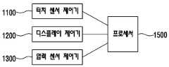
도2는 본 발명의 실시예에 따른 터치 입력 장치에서 터치 위치, 터치 압력 및 디스플레이 동작을 제어하기 위한 제어 블록을 예시한다. 디스플레이 기능 및 터치 위치 검출에 더하여 터치 압력을 검출할 수 있도록 구성된 터치 입력 장치(1000)에서 제어 블록은 전술한 터치 위치를 검출하기 위한 터치 센서 제어기(1100), 디스플레이 패널을 구동하기 위한 디스플레이 제어기(1200) 및 압력을 검출하기 위한 압력 센서 제어기(1300)를 포함하여 구성될 수 있다. 디스플레이 제어기(1200)는 터치 입력 장치(1000)의 작동을 위한 메인보드(main board) 상의 중앙 처리 유닛인 CPU(central processing unit) 또는 AP(application processor) 등으로부터 입력을 받아 디스플레이 패널(200A)에 원하는 내용을 디스플레이 하도록 하는 제어회로를 포함할 수 있다. 이러한 제어회로는 디스플레이 회로 기판(이하 디스플레이PCB로 지칭)에 실장될 수 있다. 이러한 제어회로는 디스플레이 패널 제어 IC, 그래픽 제어 IC(graphic controller IC) 및 기타 디스플레이 패널(200A) 작동에 필요한 회로를 포함할 수 있다.FIG. 2 illustrates a control block for controlling a touch position, a touch pressure, and a display operation in the touch input device according to the embodiment of the present invention. In the
압력 감지부를 통해 압력을 검출하기 위한 압력 센서 제어기(1300)는 터치 센서 제어기(1100)의 구성과 유사하게 구성되어 터치 센서 제어기(1100)와 유사하게 동작할 수 있다. 구체적으로, 압력 센서 제어기(1300)가 도1a 및 도1b에 도시된 바와 같이, 구동부, 감지부 및 제어부를 포함하고, 감지부로가 감지한 감지 신호에 의하여 압력의 크기를 검출할 수 있다. 이 때, 압력 센서 제어기(1300)는 터치 센서 제어기(1100)가 실장된 터치PCB에 실장될 수도 있고, 디스플레이 제어기(1200)가 실장된 디스플레이PCB에 실장될 수도 있다.The
실시예에 따라, 터치 센서 제어기(1100), 디스플레이 제어기(1200) 및 압력 센서 제어기(1300)는 서로 다른 구성요소로서 터치 입력 장치(1000)에 포함될 수 있다. 예컨대, 터치 센서 제어기(1100), 디스플레이 제어기(1200) 및 압력 센서 제어기(1300)는 각각 서로 다른 칩(chip)으로 구성될 수 있다. 이때, 터치 입력 장치(1000)의 프로세서(1500)는 터치 센서 제어기(1100), 디스플레이 제어기(1200) 및 압력 센서 제어기(1300)에 대한 호스트(host) 프로세서로서 기능할 수 있다.According to an embodiment, the
본 발명의 실시예에 따른 터치 입력 장치(1000)는 셀폰(cell phone), PDA(Personal Data Assistant), 스마트폰(smartphone), 태블랫 PC(tablet Personal Computer), MP3 플레이어, 노트북(notebook) 등과 같은 디스플레이 화면 및/또는 터치 스크린을 포함하는 전자 장치를 포함할 수 있다.The
이와 같은 터치 입력 장치(1000)를 얇고(slim) 경량(light weight)으로 제작하기 위해, 전술한 바와 같이 별개로 구성되는 터치 센서 제어기(1100), 디스플레이 제어기(1200) 및 압력 센서 제어기(1300)가 실시예에 따라 하나 이상의 구성으로 통합될 수 있다. 이에 더하여 프로세서(1500)에 이들 각각의 제어기가 통합되는 것도 가능하다. 이와 더불어, 실시예에 따라 디스플레이 패널(200A)에 터치 센서(10) 및/또는 압력 감지부가 통합될 수 있다.The
실시예에 따른 터치 입력 장치(1000)에서 터치 위치를 검출하기 위한 터치 센서(10)가 디스플레이 패널(200A) 외부 또는 내부에 위치할 수 있다. 실시예에 따른 터치 입력 장치(1000)의 디스플레이 패널(200A)은 액정표시장치(LCD: Liquid Crystal Display), PDP(Plasma Display Panel), 유기발광 표시장치(Organic Light Emitting Diode: OLED) 등에 포함된 디스플레이 패널일 수 있다. 이에 따라, 사용자는 디스플레이 패널에 표시된 화면을 시각적으로 확인하면서 터치 표면에 터치를 수행하여 입력 행위를 수행할 수 있다.The
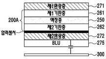
도3a 및 도3b는 본 발명의 따른 터치 입력 장치(1000)에서 디스플레이 모듈(200)의 구성을 설명하기 위한 개념도이다. 먼저, 도3a를 참조하여, LCD 패널을 이용하는 디스플레이 패널(200A)을 포함하는 디스플레이 모듈(200)의 구성을 설명하기로 한다.3A and 3B are conceptual diagrams for explaining the configuration of the
도3a에 도시된 바와 같이, 디스플레이 모듈(200)은 LCD 패널인 디스플레이 패널(200A), 디스플레이 패널(200A) 상부에 배치되는 제1편광층(271) 및 디스플레이 패널(200A) 하부에 배치되는 제2편광층(272)을 포함할 수 있다. 또한, LCD 패널인 디스플레이 패널(200A)은 액정 셀(liquid crystal cell)을 포함하는 액정층(250), 액정층(250)의 상부에 배치되는제1기판층(261) 및 액정층(250)의 하부에 배치되는 제2기판층(262)을 포함할 수 있다. 이때, 제1기판층(261)은 컬러필터 글라스(color filter glass)일 수 있고, 제2기판층(262)은 TFT 글라스(TFT glass)일 수 있다. 또한, 실시예에 따라 제1기판층(261) 및 제2기판층(262) 중 적어도 하나는 플라스틱과 같은 벤딩(bending) 가능한 물질로 형성될 수 있다. 도3a에서 제2기판층(262)은, 데이터 라인(data line), 게이트 라인(gate line), TFT, 공통 전극(Vcom: common electrode) 및 픽셀 전극(pixel electrode) 등을 포함하는 다양한 층으로 이루어질 수 있다. 이들 전기적 구성요소들은, 제어된 전기장을 생성하여 액정층(250)에 위치한 액정들을 배향시키도록 작동할 수 있다.3A, the
다음으로, 도3b를 참조하여, OLED 패널을 이용하는 디스플레이 패널(200A)을 포함하는 디스플레이 모듈(200)의 구성을 설명하기로 한다.Next, the configuration of the
도3b에 도시된 바와 같이, 디스플레이 모듈(200)은 OLED 패널인 디스플레이 패널(200A), 디스플레이 패널(200A) 상부에 배치되는 제1편광층(282)을 포함할 수 있다. 또한, OLED 패널인 디스플레이 패널(200A)은 OLED(Organic Light-Emitting Diode)를 포함하는 유기물층(280), 유기물층(280)의 상부에 배치되는 제1기판층(281) 및 유기물층(280) 하부에 배치되는 제2기판층(283)을 포함할 수 있다. 이때, 제1기판층(281)은 인캡 글라스(Encapsulation glass)일 수 있고, 제2기판층(283)은 TFT 글라스(TFT glass)일 수 있다. 또한, 실시예에 따라 제1기판층(281) 및 제2기판층(283) 중 적어도 하나는 플라스틱과 같은 벤딩(bending) 가능한 물질로 형성될 수 있다. 도3d 내지 도3f에 도시된 OLED 패널의 경우, 게이트 라인, 데이터 라인, 제1전원라인(ELVDD), 제2전원라인(ELVSS) 등의 디스플레이 패널(200A)의 구동에 사용되는 전극을 포함할 수 있다. OLED(Organic Light-Emitting Diode) 패널은 형광 또는 인광 유기물 박막에 전류를 흘리면 전자와 정공이 유기물층에서 결합하면서 빛이 발생하는 원리를 이용한 자체 발광형 디스플레이 패널로서, 발광층을 구성하는 유기물질이 빛의 색깔을 결정한다.As shown in FIG. 3B, the
구체적으로, OLED는 유리나 플라스틱 위에 유기물을 도포해 전기를 흘리면, 유기물이 광을 발산하는 원리를 이용한다. 즉, 유기물의 양극과 음극에 각각 정공과 전자를 주입하여 발광층에 재결합시키면 에너지가 높은 상태인 여기자(excitation)를 형성하고, 여기자가 에너지가 낮은 상태로 떨어지면서 에너지가 방출되어 특정한 파장의 빛이 생성되는 원리를 이용하는 것이다. 이때, 발광층의 유기물에 따라 빛의 색깔이 달라진다.Specifically, OLEDs use the principle that an organic material emits light when an organic material is applied to glass or plastic and electricity is supplied. That is, when holes and electrons are injected into the anode and the cathode of the organic material, respectively, and then recombined with the light emitting layer, excitons having a high energy state are formed. When excitons fall into a state of low energy, energy is emitted, And to use the generated principle. At this time, the color of the light changes depending on the organic material of the light emitting layer.
OLED는 픽셀 매트릭스를 구성하고 있는 픽셀의 동작특성에 따라 라인 구동 방식의 PM-OLED(Passive-matrix Organic Light-Emitting Diode)와 개별 구동 방식의 AM-OLED(Active-matrix Organic Light-Emitting Diode)가 존재한다. 양자 모두 백라이트를 필요로 하지 않기 때문에 디스플레이 모듈을 매우 얇게 구현할 수 있고, 각도에 따라 명암비가 일정하고, 온도에 따른 색 재현성이 좋다는 장점을 갖는다. 또한, 미구동 픽셀은 전력을 소모하지 않는다는 점에서 매우 경제적이다.In OLED, a line-driven PM-OLED (Passive-matrix Organic Light-Emitting Diode) and an AM-OLED (Active-matrix Organic Light-Emitting Diode) are used depending on the operation characteristics of the pixels constituting the pixel matrix exist. Since both of them do not require a backlight, the display module can be made very thin, the contrast ratio is constant according to the angle, and color reproducibility according to temperature is good. In addition, un-driven pixels are very economical in that they do not consume power.
동작 면에서 PM-OLED는 높은 전류로 스캐닝 시간(scanning time) 동안만 발광을 하고, AM-OLED는 낮은 전류로 프레임 시간(frame time)동안 계속 발광 상태를 유지한다. 따라서, AM-OLED는 PM-OLED에 비해서 해상도가 좋고, 대면적 디스플레이 패널 구동이 유리하며, 전력 소모가 적다는 장점이 있다. 또한, 박막 트랜지스터(TFT)를 내장하여 각 소자를 개별적으로 제어할 수 있기 때문에 정교한 화면을 구현하기 쉽다.In operation, the PM-OLED emits light only for a scanning time with a high current, and the AM-OLED maintains a light emission state for a frame time with a low current. Therefore, AM-OLED has better resolution than PM-OLED, it is advantageous to drive a large-area display panel and has low power consumption. In addition, since each element can be individually controlled by incorporating a thin film transistor (TFT), it is easy to realize a sophisticated screen.
또한, 유기물층(280)은 HIL(Hole Injection Layer, 정공주입층), HTL(Hole Transfer Layer, 정공수송층), EIL(Emission Material Layer, 전자주입층), ETL(Electron Transfer Layer, 전자수송층), EML(Electron Injection Layer, 발광층)을 포함할 수 있다.The
각 층에 대해 간략히 설명하면, HIL은 정공을 주입시키며, CuPc 등의 물질을 이용한다. HTL은 주입된 정공을 이동시키는 기능을 하고, 주로, 정공의 이동성(hole mobility)이 좋은 물질을 이용한다. HTL은 아릴라민(arylamine), TPD 등이 이용될 수 있다. EIL과 ETL은 전자의 주입과 수송을 위한 층이며, 주입된 전자와 정공은 EML에서 결합되어 발광한다. EML은 발광되는 색을 표현하는 소재로서, 유기물의 수명을 결정하는 호스트(host)와 색감과 효율을 결정하는 불순물(dopant)로 구성된다. 이는, OLED 패널에 포함되는 유기물층(280)의 기본적인 구성을 설명한 것일 뿐, 본 발명은 유기물층(280)의 층구조나 소재 등에 한정되지 않는다.Briefly describing each layer, the HIL injects holes, and uses a material such as CuPc. The HTL functions to transfer injected holes, and mainly uses materials having good hole mobility. HTL may be arylamine, TPD, or the like. EIL and ETL are layers for electron injection and transport, and injected electrons and holes are combined in EML to emit light. EML is a material that expresses the emitted color, and is composed of a host that determines the lifetime of the organic material, and a dopant that determines color and efficiency. This is only a description of the basic structure of the
유기물층(280)은 애노드(Anode)(미도시)와 캐소드(Cathode)(미도시) 사이에 삽입되며, TFT가 온(On) 상태가 되면, 구동 전류가 애노드에 인가되어 정공이 주입되고 캐소드에는 전자가 주입되어, 유기물층(280)으로 정공과 전자가 이동하여 빛을 발산한다.The
당해 기술분야의 당업자에게는, LCD 패널 또는 OLED 패널이 디스플레이 기능을 수행하기 위해 다른 구성을 더 포함할 수 있으며 변형이 가능함이 자명할 것이다.It will be apparent to those skilled in the art that an LCD panel or an OLED panel may further include other configurations for performing the display function and may be modified.
본 발명에 따른 터치 입력 장치(1000)의 디스플레이 모듈(200)은 디스플레이 패널(200A) 및 디스플레이 패널(200A)를 구동하기 위한 구성을 포함할 수 있다. 구체적으로, 디스플레이 패널(200A)이 LCD 패널인 경우, 디스플레이 모듈(200)은 제2편광층(272) 하부에 배치되는 백라이트 유닛(미도시: backlight unit)을 포함하여 구성될 수 있고, LCD패널의 작동을 위한 디스플레이 패널 제어 IC, 그래픽 제어 IC 및 기타 회로를 더 포함할 수 있다.The
본 발명에 따른 터치 입력 장치(1000)의 디스플레이 모듈(200)은 디스플레이 패널(200A) 및 디스플레이 패널(200A)를 구동하기 위한 구성을 포함할 수 있다. 구체적으로, 디스플레이 패널(200A)이 LCD 패널인 경우, 디스플레이 모듈(200)은 제2편광층(272) 하부에 배치되는 백라이트 유닛(미도시: backlight unit)을 포함하여 구성될 수 있고, LCD패널의 작동을 위한 디스플레이 패널 제어 IC, 그래픽 제어 IC 및 기타 회로를 더 포함할 수 있다.The
본 발명의 실시예에 따른 터치 입력 장치(1000)에서 터치 위치를 검출하기 위한 터치 센서(10)는 디스플레이 모듈(200) 외부 또는 내부에 위치할 수 있다.The
터치 입력 장치(1000)에서 터치 센서(10)가 디스플레이 모듈(200)의 외부에 배치되는 경우, 디스플레이 모듈(200) 상부에는 터치 센서 패널이 배치될 수 있고, 터치 센서(10)가 터치 센서 패널에 포함될 수 있다. 터치 입력 장치(1000)에 대한 터치 표면은 터치 센서 패널의 표면일 수 있다.In the case where the
터치 입력 장치(1000)에서 터치 센서(10)가 디스플레이 모듈(200)의 내부에 배치되는 경우, 터치 센서(10)가 디스플레이 패널(200A) 외부에 위치하도록 구성될 수 있다. 구체적으로, 터치 센서(10)가 제1기판층(261,281)의 상면에 형성될 수 있다. 이때, 터치 입력 장치(1000)에 대한 터치 표면은 디스플레이 모듈(200)의 외면으로서 도3a 및 도3b에서 상부면 또는 하부면이 될 수 있다.When the
터치 입력 장치(1000)에서 터치 센서(10)가 디스플레이 모듈(200)의 내부에 배치되는 경우, 실시예에 따라 터치 센서(10) 중 적어도 일부는 디스플레이 패널(200A) 내에 위치하도록 구성되고 터치 센서(10) 중 적어도 나머지 일부는 디스플레이 패널(200A) 외부에 위치하도록 구성될 수 있다. 예컨대, 터치 센서(10)를 구성하는 구동전극(TX)과 수신전극(RX) 중 어느 하나의 전극은 디스플레이 패널(200A) 외부에 위치하도록 구성될 수 있으며, 나머지 전극은 디스플레이 패널(200A) 내부에 위치하도록 구성될 수도 있다. 구체적으로, 터치 센서(10)를 구성하는 구동전극(TX)과 수신전극(RX) 중 어느 하나의 전극은 제1기판층(261,281) 상면에 형성될 수 있으며, 나머지 전극은 제1기판층(261,281) 하면 또는 제2기판층(262,283) 상면에 형성될 수 있다.In the case where the
터치 입력 장치(1000)에서 터치 센서(10)가 디스플레이 모듈(200)의 내부에 배치되는 경우, 터치 센서(10)가 디스플레이 패널(200A) 내부에 위치하도록 구성될 수 있다. 구체적으로, 터치 센서(10)가 제1기판층(261,281)의 하면 또는 제2기판층(262,283)의 상면에 형성될 수 있다.When the
디스플레이 패널(200A) 내부에 터치 센서(10)가 배치되는 경우, 터치 센서 동작을 위한 전극이 추가로 배치될 수도 있으나, 디스플레이 패널(200A) 내부에 위치하는 다양한 구성 및/또는 전극이 터치 센싱을 위한 터치 센서(10)로 이용될 수도 있다. 구체적으로, 디스플레이 패널(200A)이 LCD 패널인 경우, 터치 센서(10)에 포함되는 전극 중 적어도 어느 하나는 데이터 라인(data line), 게이트 라인(gate line), TFT, 공통 전극(Vcom: common electrode) 및 픽셀 전극(pixel electrode) 중 적어도 어느 하나를 포함할 수 있고, 디스플레이 패널(200A)이 OLED 패널인 경우, 터치 센서(10)에 포함되는 전극 중 적어도 어느 하나는 데이터 라인(data line), 게이트 라인(gate line), 제1전원라인(ELVDD) 및 제2전원라인(ELVSS) 중 적어도 어느 하나를 포함할 수 있다.In the case where the
이 때, 터치 센서(10)는 도1a에서 설명된 구동전극 및 수신전극으로 동작하여 구동전극 및 수신전극 사이의 상호정전용량에 따라 터치 위치를 검출할 수 있다. 또한, 터치 센서(10)는 도1b에서 설명된 단일 전극(30)으로 동작하여 단일 전극(30) 각각의 자기정전용량에 따라 터치 위치를 검출할 수 있다. 이 때, 터치 센서(10)에 포함되는 전극이 디스플레이 패널(200A)의 구동에 사용되는 전극일 경우, 제1 시간구간에 디스플레이 패널(200A)을 구동하고, 제1 시간구간과 다른 제2 시간구간에 터치 위치를 검출할 수 있다.At this time, the
본 발명의 터치 입력 장치(1000)에서 터치 위치를 검출하기 위한 터치 센서가 형성된 커버층(100)과 디스플레이 패널(200A)을 포함하는 디스플레이 모듈(200) 사이가 OCA(Optically Clear Adhesive)와 같은 접착제로 라미네이션되어 있을 수 있다. 이에 따라 터치 센서의 터치 표면을 통해 확인할 수 있는 디스플레이 모듈(200)의 디스플레이 색상 선명도, 시인성 및 빛 투과성이 향상될 수 있다.The
이하에서는 본 발명의 실시예에 따른 터치 입력 장치에서 입력 영역 영역에 인가되는 터치 압력의 크기를 검출하기 위하여, 입력 영역에 인접한 위치에 배치된 센서를 압력 감지부로 사용하는 경우에 대해서 예를 들어 상세하게 살펴본다.Hereinafter, in order to detect the magnitude of the touch pressure applied to the input area in the touch input device according to the embodiment of the present invention, a case where the sensor disposed at a position adjacent to the input area is used as the pressure sensing part will be described in detail .
도4a는 본 발명의 실시예에 따른 터치 입력 장치의 사시도이고, 도4b 내지 도4e는 본 발명의 실시예에 따른 터치 입력 장치의 평면도이다.4A is a perspective view of a touch input device according to an embodiment of the present invention, and FIGS. 4B through 4E are plan views of a touch input device according to an embodiment of the present invention.
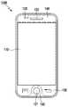
도4b 내지 도4e에 도시된 바와 같이, 본 발명에 따른 터치 입력 장치(1000)는 디스플레이 영역(110) 및 입력 영역을 포함할 수 있다. 이 때, 입력 영역은 홈키(121), 스피커(122), 카메라(123), 뒤로가기키 및 메뉴키 등일 수 있다. 구체적으로, 터치 입력 장치(1000)에 포함된 커버층(100)이 디스플레이 영역(110) 및 입력 영역을 포함할 수 있다. 또한, 커버층(100)의 디스플레이 영역(110) 하부에는 디스플레이 패널(200A)이 배치될 수 있다.4B to 4E, the
도4b에 도시된 바와 같이, 본 발명에 따른 터치 입력 장치(1000)는 비-디스플레이 영역(120)을 더 포함할 수 있다. 구체적으로, 터치 입력 장치(1000)에 포함된 커버층(100)이 디스플레이 영역(110) 및 비-디스플레이 영역(120)을 포함할 수 있다. 또한, 커버층(100)의 디스플레이 영역(110) 하부에는 디스플레이 패널(200A)이 배치될 수 있고, 커버층(100)의 비-디스플레이 영역(120) 하부에는 디스플레이 패널(200A)이 배치되지 않을 수 있다. 이 때, 입력 영역이 비-디스플레이 영역(120) 내에 배치될 수 있다.As shown in FIG. 4B, the
도4c에 도시된 바와 같이, 본 발명에 따른 터치 입력 장치(1000)는 터치 위치 센싱 영역(130) 및 비-터치 위치 센싱 영역(140)을 포함할 수 있다. 이 때, 터치 위치 센싱 영역(130)은 디스플레이 영역(110)과 같을 수도 있고, 다를 수도 있다. 마찬가지로, 비-터치 위치 센싱 영역(140)은 비-디스플레이 영역(120)과 같을 수도 있고, 다를 수도 있다. 이 때, 도4c에 도시된 바와 같이, 터치 위치 센싱 영역(130)이 디스플레이 영역(110)을 포함할 수 있다. 구체적으로, 터치 위치 센싱 영역(130)이 디스플레이 영역(110)과 같은 경우, 터치 위치를 검출하기 위한 터치 센서(10)가 디스플레이 영역(110)의 하부에 배치될 수 있다. 구체적으로, 터치 센서(10)가 커버층(100)의 디스플레이 영역(110) 하부에 일체형으로 형성될 수도 있고, 디스플레이 영역(110) 하부에 배치되는 디스플레이 패널(200)에 포함될 수도 있다. 터치 위치 센싱 영역(130)이 디스플레이 영역(110)과 다른 경우, 터치 위치를 검출하기 위한 터치 센서(10)가 커버층(100)의 비-디스플레이 영역(120) 하부에 배치될 수 있다. 구체적으로, 터치 센서(10)가 커버층(100)의 비-디스플레이 영역(110) 하부에 일체형으로 형성될 수 있다.As shown in FIG. 4C, the
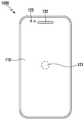
도4d에 도시된 바와 같이, 본 발명에 따른 터치 입력 장치(1000)의 입력 영역이 디스플레이 영역(110) 내에 배치될 수 있다. 또한, 도4e에 도시된 바와 같이, 본 발명에 따른 터치 입력 장치(1000)의 전체 영역에 디스플레이 영역(110)이 배치될 수 있다. 구체적으로, 터치 입력 장치(1000)에 포함된 커버층(100)의 전체 영역이 디스플레이 영역(110)일 수 있다. 이 때, 마찬가지로, 본 발명에 따른 터치 입력 장치(1000)의 입력 영역이 디스플레이 영역(110) 내에 배치될 수 있다.4D, an input area of the
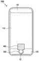
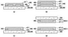
도5a 내지 도5h는 압력 감지부가 배치된 본 발명의 실시예에 따른 터치 입력 장치를 아래쪽에서 바라본 도면이다. 구제척으로, 도5a 내지 도5h는 본 발명에 따른 터치 입력 장치(1000)의 디스플레이 패널(200A) 하부에 배치된 압력 감지부의 압력 센서(450)가 보일 수 있도록, 기판(300) 및 하우징(320)이 제거된 상태의 터치 입력 장치(1000)를 아래쪽에서 바라본 도면이다.5A to 5H are views of a touch input device according to an embodiment of the present invention in which a pressure sensing part is disposed, from below. 5A to 5H illustrate the
도6a 내지 도6e, 도7a 내지 도7j, 및 도8은 도4a에 도시된 본 발명의 실시예에 따른 터치 입력 장치의 B-B' 단면도이다. 구체적으로 도6a 내지 도6e는 디스플레이 패널(200A)로서 OLED 패널이 적용된 도4a에 도시된 본 발명의 실시예에 따른 터치 입력 장치의 B-B' 단면도이고, 7a 내지 도7j는 디스플레이 패널(200A)로서 LCD 패널이 적용된 도4a에 도시된 본 발명의 실시예에 따른 터치 입력 장치의 B-B' 단면도이고, 도8은 도5c에 도시된 압력 센서가 구비된 도4a에 도시된 터치 입력 장치(1000)의 B-B'단면도이다.6A to 6E, 7A to 7J, and 8 are cross-sectional views taken along the line B-B 'of the touch input device according to the embodiment of the present invention shown in FIG. 4A. 6A to 6E are cross-sectional views of the touch input device according to the embodiment of the present invention shown in FIG. 4A to which an OLED panel is applied as a
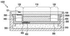
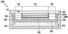
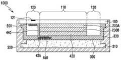
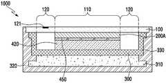
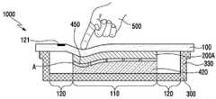
도5a, 도6a, 도7a 및 도7b에 도시된 바와 같이, 본 발명에 따른 압력 감지부는 디스플레이 영역(110)에 배치될 수 있다. 구체적으로, 압력 감지부에 포함된 압력 센서(450)는 디스플레이 영역(110) 중 비-디스플레이 영역(120) 내에 배치된 입력 영역에 인접한 위치에 배치되되, 디스플레이 패널(200A) 하부에 배치될 수 있다. 또한, 압력 센서(450)가 디스플레이 패널(200A) 하면에 일체형으로 형성될 수 있다. 이 때, 도5f에 도시된 바와 같이, 압력 센서(450)로부터 연장된 트레이스(451)를 통하여 압력 센서(450)가 제1PCB(160)에 전기적으로 연결될 수 있다. 또한, 트레이스(451)도 압력 센서(450)와 마찬가지로 디스플레이 패널(200A) 하면에 직접 형성될 수 있다. 여기서 제1PCB(160)은 터치PCB일 수도 있고, 디스플레이PCB일 수도 있다. 또한, 압력 센서(450)는 제1PCB(160)에 형성된 제1연결부(170)를 통하여 메인보드에 전기적으로 연결될 수 있다. 또한, 본 발명에 따른 터치 입력 장치(1000)는 비-디스플레이 영역(120) 내에 배치된 입력 영역에 터치가 입력되는지를 검출하는 별도의 터치 센서를 더 포함할 수 있다. 구체적으로, 도5a, 도5f, 도6a 및 도7a에 도시된 홈키(121)에 터치가 입력되는지를 검출하는 별도의 터치 센서(미도시)를 더 포함할 수 있다. 이 때, 별도의 터치 센서(미도시)는 단순히 터치 여부를 검출하는 센서일 수도 있고, 사용자의 인증을 할 수 있는 기능을 포함하는 사용자 인증 센서일 수도 있다. 예를 들면 지문 인식 센서일 수 있다. 이 경우, 압력 센서(450)는 디스플레이 영역(110)의 일부에만 배치되므로, 디스플레이 영역(110)에 인가되는 압력의 크기는 검출하지 않고, 비-디스플레이 영역(120) 내에 배치된 입력 영역에 인가되는 압력의 크기만 검출할 수 있다. 도6a에 도시된 바와 같이, 디스플레이 패널(200A)로서 OLED 패널이 적용된 경우, 제2기판층(283) 하면에 압력 센서(450)가 직접 형성될 수 있고, 본 발명에 따른 터치 입력 장치(1000)는 압력 센서(450)와 기판(300) 사이에 배치된 스페이서층(420)을 포함할 수 있다. 도7a 및 7b에 도시된 바와 같이, 디스플레이 패널(200A)로서 LCD 패널이 적용된 경우, 제2기판층(262) 하면 또는 제2편광층(272) 하면에 압력 센서(450)가 직접 형성될 수 있고, 본 발명에 따른 터치 입력 장치(1000)는 제2편광층(272) 하부에 배치된 백라이트 유닛(200B)을 더 포함할 수 있다. 또한, 도7a에 도시된 바와 같이, 본 발명에 따른 터치 입력 장치(1000)는 백라이트 유닛(200B)과 기판(300) 사이에 배치된 스페이서층(420)을 포함할 수 있고, 도7b에 도시된 바와 같이, 본 발명에 따른 터치 입력 장치(1000)는 백라이트 유닛(200B) 하부에 배치되고 디스플레이 패널(200A) 및 백라이트 유닛(200B)을 감싸는 서스캔(350) 및 서스캔(350)과 기판(300) 사이에 배치된 스페이서층(420)을 포함할 수 있다. 이 때, 서스캔(350)은 디스플레이 패널(200A)과 백라이트 유닛(200B)를 보호하는 기능을 하며, 커버층(100) 또는 디스플레이 패널(200A)에 고정될 수 있다.As shown in FIGS. 5A, 6A, 7A and 7B, the pressure sensing unit according to the present invention may be disposed in the
도5b, 도6b 및 도7c에 도시된 바와 같이, 본 발명에 따른 압력 감지부는 센서시트(440)의 형태로 디스플레이 영역(110)에 배치될 수 있다. 구체적으로, 압력 센서(450)를 포함하는 센서시트(440)는 디스플레이 영역(110) 중 비-디스플레이 영역(120) 내에 배치된 입력 영역에 인접한 위치에 배치되되, 디스플레이 패널(200A) 하부에 부착될 수 있다. 도6b에 도시된 바와 같이, 디스플레이 패널(200A)로서 OLED 패널이 적용된 경우, 제2기판층(283) 하면에 센서시트(440)가 부착될 수 있고, 본 발명에 따른 터치 입력 장치(1000)는 센서시트(440)와 기판(300) 사이에 배치된 스페이서층(420)을 포함할 수 있다. 도7c에 도시된 바와 같이, 디스플레이 패널(200A)로서 LCD 패널이 적용된 경우, 본 발명에 따른 터치 입력 장치(1000)는 디스플레이 패널(200A) 하부에 배치된 백라이트 유닛(200B), 백라이트 유닛(200B) 하부에 배치되고 하면에 센서시트(440)가 부착된 서스캔(350) 및 센서시트(440)와 기판(300) 사이에 배치된 스페이서층(420)을 포함할 수 있다.5B, 6B, and 7C, the pressure sensing unit according to the present invention may be disposed in the
도5b, 도6c 내지 도6e 및 도7d 내지 도7i에 도시된 바와 같이, 본 발명에 따른 압력 감지부는 센서시트(440)의 형태로 디스플레이 영역(110)에 배치될 수 있다. 구체적으로, 압력 센서(450)를 포함하는 센서시트(440)는 디스플레이 영역(110) 중 비-디스플레이 영역(120) 내에 배치된 입력 영역에 인접한 위치에 배치되되, 기판(300) 상부에 부착될 수 있다. 도6c 내지 도6e에 도시된 바와 같이, 디스플레이 패널(200A)로서 OLED 패널이 적용된 경우, 본 발명에 따른 터치 입력 장치(1000)는 센서시트(440)와 디스플레이 패널(200A) 사이에 배치된 스페이서층(420)을 포함할 수 있다. 도7d 내지 도7i에 도시된 바와 같이, 디스플레이 패널(200A)로서 LCD 패널이 적용된 경우, 본 발명에 따른 터치 입력 장치(1000)는 디스플레이 패널(200A) 하부에 배치된 백라이트 유닛(200B), 백라이트 유닛(200B)과 센서시트(440) 사이에 배치된 스페이서층(420)을 포함할 수 있다. 이 때, 도7e, 도7g 및 도7i에 도시된 바와 같이, 본 발명에 따른 터치 입력 장치(1000)는 백라이트 유닛(200B)과 스페이서층(420) 사이에 배치된 서스캔(350)을 더 포함할 수도 있다. 여기서, 도7f 내지 도7i에 도시된 바와 같이, 본 발명에 따른 터치 입력 장치(1000)의 기판(300)에 센서홈(301)이 형성되고, 센서시트(440)의 적어도 일부가 센서홈(301)에 삽입될 수 있다. 이 때, 센서홈(301)에 삽입되는 센서시트(440)의 일부에는 압력 센서(450)가 배치될 수 있다. 이 때, 센서홈(301)에 센서시트(440)가 삽입된 상태에서 센서시트(440)의 상면과 기판(300)의 센서홈(301)이 배치되지 않은 영역의 상면이 동일한 평면상에 위치할 수 있다. 이와 같이, 센서홈(301)에 센서시트(440)가 삽입된 상태에서 센서시트(440)의 상면과 기판(300)의 센서홈(301)이 배치되지 않은 영역의 상면이 동일한 평면상에 위치할 경우, 센서시트(440) 상부에 배치되는 스페이서층(420)의 영역 및 센서시트(440)가 배치되지 않은 기판(300) 상부에 배치되는 스페이서층(420)의 영역에서의 스페이서층(420)의 두께가 동일한 장점이 있다. 이 때, 도7f 및 도7g에 도시된 바와 같이, 센서시트(440)의 두께가 센서홈(301)의 깊이와 같을 수 있다. 또한, 도7h 및 도7i에 도시된 바와 같이 본 발명에 따른 터치 입력 장치(1000)는 센서홈(301)에 삽입되고, 센서홈(301)에 삽입된 센서시트(440)의 하부에 배치되는 홈스페이서층(425)을 더 포함할 수 있다. 이 경우, 센서시트(440)의 두께와 홈스페이서층(425)의 두께를 합한 값이 센서홈(301)의 깊이와 같을 수 있다.5B, 6C to 6E, and 7D to 7I, the pressure sensing unit according to the present invention may be disposed in the
도5b 및 도7j에 도시된 바와 같이, 본 발명에 따른 압력 감지부는 센서시트(440)의 형태로 디스플레이 영역(110)에 배치될 수 있다. 구체적으로 도7j에 도시된 바와 같이, 디스플레이 패널(200A)로서 LCD 패널이 적용된 경우, 본 발명에 따른 터치 입력 장치(1000)는 디스플레이 패널(200A) 하부에 배치된 백라이트 유닛(200B), 백라이트 유닛(200B) 하부에 배치된 서스캔(350) 및 서스캔(350)과 기판(300) 사이에 배치된 스페이서층(420)을 포함할 수 있다. 이 때, 센서 시트(440)는 백라이트 유닛(200B)와 이격되어 서스캔(350)의 상면에 배치될 수 있다. 이 경우, 센서시트(440)와 백라이트 유닛(200B) 사이에 추가의 스페이서층(미도시)이 배치될 수도 있다.5B and 7J, the pressure sensing unit according to the present invention may be disposed in the
이 때, 도5g에 도시된 바와 같이, 압력 센서(450)는 압력 센서(450)를 포함하는 센서시트(440)에 형성된 제2연결부(180)를 통하여 메인보드에 전기적으로 연결될 수 있다. 또한, 센서시트(440)는 비-디스플레이 영역(120) 내에 배치된 입력 영역에 터치가 입력되는지를 검출하는 별도의 터치 센서를 더 포함할 수 있다. 즉, 별도의 터치 센서는 비-디스플레이 영역(110) 내에 배치된 입력 영역 하부에 배치되고 압력 감지부와 일체로 형성될 수 있다. 구체적으로, 도5b 및 도5g에 도시된 바와 같이, 센서시트(440)는 홈키(121)에 터치가 입력되는지를 검출하는 별도의 터치 센서(550)를 더 포함할 수 있다. 이 때, 별도의 터치 센서(550)는 단순히 터치 여부를 검출하는 센서일 수도 있고, 사용자의 인증을 할 수 있는 기능을 포함하는 사용자 인증 센서일 수도 있다. 예를 들면 지문 인식 센서일 수 있다. 이 경우, 압력 센서(450)는 디스플레이 영역(110)의 일부에만 배치되므로, 디스플레이 영역(110)에 인가되는 압력의 크기는 검출하지 않고, 비-디스플레이 영역(120) 내에 배치된 입력 영역에 인가되는 압력만 검출할 수 있다.5G, the
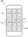
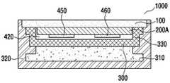
도5c 및 도8에 도시된 바와 같이, 본 발명에 따른 압력 센서(450)는 디스플레이 영역(110)에 배치될 수 있다. 구체적으로, 압력 센서(450)는 디스플레이 영역(110)의 전체 영역에 걸쳐 배치될 수 있다. 이 경우, 압력 센서(450)는 디스플레이 영역(110)의 전체 영역에 걸쳐 배치되므로, 디스플레이 영역(110)에 인가되는 압력도 검출하고, 비-디스플레이 영역(120) 내에 배치된 입력 영역에 인가되는 압력도 검출할 수 있다. 구체적으로, 도5c 및 도8에 도시된 바와 같이, 복수의 압력센서(450)를 이용하여 디스플레이 영역(110)에 인가되는 압력의 크기를 검출하고, 압력 센서(450) 중 비-디스플레이 영역(120) 내에 배치된 입력 영역과 인접한 위치에 배치된 압력 센서(A)를 이용하여 비-디스플레이 영역(120) 내에 배치된 입력 영역에 인가되는 압력을 검출할 수 있다. 예를 들면 홈키(121)와 인접한 위치에 배치된 압력 센서(A)를 이용하여 홈키(121)에 인가되는 압력의 크기를 검출할 수 있다. 마찬가지로, 별도의 터치 센서(미도시)를 더 포함할 수 있으며, 별도의 터치 센서는 단순히 터치 여부를 검출하는 센서일 수도 있고, 사용자의 인증을 할 수 있는 기능을 포함하는 사용자 인증 센서일 수도 있다. 도8에서는 압력 센서(450)가 디스플레이 패널(200A) 하면에 직접 형성된 것으로 설명되었으나, 이에 한정하지 않으며, 압력 센서(450)가 센서시트(440)의 형태로 디스플레이 패널(200A)하면에 부착될 수도 있고, 기판(300) 상면에 부착될 수도 있다. 또한, 디스플레이 패널(200A)이 OLED 패널뿐만 아니라 LCD 패널인 경우에도 적용 가능하다.5c and 8, the
본 발명에 따른 터치 입력 장치(1000)는 비-디스플레이 영역(120)내에 배치된 입력 영역에 배치되는 별도의 터치 센서(550) 없이도 비-디스플레이 영역(120) 내에 배치된 입력 영역에 압력이 인가되는지를 판단할 수 있다. 터치 위치 센싱 영역(130)이 디스플레이 영역(110)과 같은 경우, 디스플레이 영역(110) 하부에 배치된 터치 센서(10)에 의하여 터치 위치가 감지되지 않으면, 압력이 비-디스플레이 영역(120) 내에 배치된 입력 영역에 인가되는 것으로 판단할 수 있다. 터치 위치 센싱 영역(130)이 디스플레이 영역(110)과 다를 경우, 비-디스플레이 영역(120) 내에 배치된 입력 영역 하부에 배치된 터치 센서(10)에 의하여 터치 위치가 감지되면, 압력이 비-디스플레이 영역(120) 내에 배치된 입력 영역에 인가되는 것으로 판단할 수 있다. 또한, 도4c에 도시된 바와 같이, 터치 위치 센싱 영역(130)이 디스플레이 영역(110)을 포함하는 경우, 터치 센서(10)에 의하여 터치 위치가 감지되지 않는 경우, 압력이 비-디스플레이 영역(120) 내에 배치된 입력 영역에 인가되는 것으로 판단할 수 있다.The
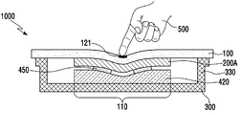
도5d에 도시된 바와 같이, 본 발명에 따른 압력 감지부는 디스플레이 영역(110)에 배치될 수 있다. 구체적으로, 압력 감지부에 포함된 압력 센서(450)는 디스플레이 영역(110) 내에 배치된 입력 영역에 인접한 위치에 배치되되, 디스플레이 패널(200A) 하부에 배치될 수 있다. 또한, 압력 센서(450)가 디스플레이 패널(200A) 하면에 일체형으로 형성될 수 있다. 이 때, 도5h에 도시된 바와 같이, 압력 센서(450)로부터 연장된 트레이스(451)를 통하여 압력 센서(450)가 제1PCB(160)에 전기적으로 연결될 수 있다. 또한, 트레이스(451)도 압력 센서(450)와 마찬가지로 디스플레이 패널(200A) 하면에 직접 형성될 수 있다. 여기서 제1PCB(160)은 터치PCB일 수도 있고, 디스플레이PCB일 수도 있다. 또한, 압력 센서(450)는 제1PCB(160)에 형성된 제1연결부(170)를 통하여 메인보드에 전기적으로 연결될 수 있다. 또한, 본 발명에 따른 터치 입력 장치(1000)는 디스플레이 영역(110) 내에 배치된 입력 영역에 터치가 입력되는지를 검출할 수 있다. 구체적으로, 디스플레이 영역(110) 내에 배치된 입력 영역 하부에 배치된 터치 센서(10)에 의하여 터치 위치가 감지되면, 압력이 디스플레이 영역(110) 내에 배치된 입력 영역에 인가되는 것으로 판단할 수 있다. 또한, 본 발명에 따른 터치 입력 장치(1000)는 입력 영역에 터치가 입력되는지를 검출하는 별도의 사용자의 인증을 할 수 있는 기능을 포함하는 사용자 인증 센서를 더 포함할 수 있다. 이 때, 사용자 인증 센서는 예를 들면 지문 인식 센서일 수 있다. 이 경우에도 전술한 도6a 내지 도6e, 도7a 내지 도7j과 같은 형태로 압력 센서(450)가 배치될 수 있다. 구체적으로, 도6a에 도시된 바와 같이, 디스플레이 패널(200A)로서 OLED 패널이 적용된 경우, 제2기판층(283) 하면에 압력 센서(450)가 직접 형성될 수 있고, 본 발명에 따른 터치 입력 장치(1000)는 압력 센서(450)와 기판(300) 사이에 배치된 스페이서층(420)을 포함할 수 있다. 도7a 및 7b에 도시된 바와 같이, 디스플레이 패널(200A)로서 LCD 패널이 적용된 경우, 제2기판층(262) 하면 또는 제2편광층(272) 하면에 압력 센서(450)가 직접 형성될 수 있고, 본 발명에 따른 터치 입력 장치(1000)는 제2편광층(272) 하부에 배치된 백라이트 유닛(200B)을 더 포함할 수 있다. 또한, 도7a에 도시된 바와 같이, 본 발명에 따른 터치 입력 장치(1000)는 백라이트 유닛(200B)과 기판(300) 사이에 배치된 스페이서층(420)을 포함할 수 있고, 도7b에 도시된 바와 같이, 본 발명에 따른 터치 입력 장치(1000)는 백라이트 유닛(200B) 하부에 배치되고 디스플레이 패널(200A) 및 백라이트 유닛(200B)을 감싸는 서스캔(350) 및 서스캔(350)과 기판(300) 사이에 배치된 스페이서층(420)을 포함할 수 있다. 이 때, 서스캔(350)은 디스플레이 패널(200A)과 백라이트 유닛(200B)를 보호하는 기능을 하며, 커버층(100) 또는 디스플레이 패널(200A)에 고정될 수 있다.As shown in FIG. 5D, the pressure sensing unit according to the present invention may be disposed in the
또한, 도6b 및 도7c에 도시된 바와 같이, 본 발명에 따른 압력 감지부는 센서시트(440)의 형태로 디스플레이 영역(110)에 배치될 수 있다. 구체적으로, 압력 센서(450)를 포함하는 센서시트(440)는 디스플레이 영역(110) 중 입력 영역, 예를 들어 홈키(121)에 인접한 위치에 배치되되, 디스플레이 패널(200A) 하부에 부착될 수 있다. 도6b에 도시된 바와 같이, 디스플레이 패널(200A)로서 OLED 패널이 적용된 경우, 제2기판층(283) 하면에 센서시트(440)가 부착될 수 있고, 본 발명에 따른 터치 입력 장치(1000)는 센서시트(440)와 기판(300) 사이에 배치된 스페이서층(420)을 포함할 수 있다. 도7c에 도시된 바와 같이, 디스플레이 패널(200A)로서 LCD 패널이 적용된 경우, 본 발명에 따른 터치 입력 장치(1000)는 디스플레이 패널(200A) 하부에 배치된 백라이트 유닛(200B), 백라이트 유닛(200B) 하부에 배치되고 하면에 센서시트(440)가 부착된 서스캔(350) 및 센서시트(440)와 기판(300) 사이에 배치된 스페이서층(420)을 포함할 수 있다.6 (b) and 7 (c), the pressure sensing unit according to the present invention may be disposed in the
도6c 내지 도6e 및 도7d 내지 도7i에 도시된 바와 같이, 본 발명에 따른 압력 감지부는 센서시트(440)의 형태로 디스플레이 영역(110)에 배치될 수 있다. 구체적으로, 압력 센서(450)를 포함하는 센서시트(440)는 디스플레이 영역(110) 중 입력 영역, 예를 들어 홈키(121)에 인접한 위치에 배치되되, 기판(300) 상부에 부착될 수 있다. 도6c 내지 도6e에 도시된 바와 같이, 디스플레이 패널(200A)로서 OLED 패널이 적용된 경우, 본 발명에 따른 터치 입력 장치(1000)는 센서시트(440)와 디스플레이 패널(200A) 사이에 배치된 스페이서층(420)을 포함할 수 있다. 도7d 내지 도7i에 도시된 바와 같이, 디스플레이 패널(200A)로서 LCD 패널이 적용된 경우, 본 발명에 따른 터치 입력 장치(1000)는 디스플레이 패널(200A) 하부에 배치된 백라이트 유닛(200B), 백라이트 유닛(200B)과 센서시트(440) 사이에 배치된 스페이서층(420)을 포함할 수 있다. 이 때, 도7e, 도7g 및 도7i에 도시된 바와 같이, 본 발명에 따른 터치 입력 장치(1000)는 백라이트 유닛(200B)과 스페이서층(420) 사이에 배치된 서스캔(350)을 더 포함할 수도 있다. 여기서, 도7f 내지 도7i에 도시된 바와 같이, 본 발명에 따른 터치 입력 장치(1000)의 기판(300)에 센서홈(301)이 형성되고, 센서시트(440)의 적어도 일부가 센서홈(301)에 삽입될 수 있다. 이 때, 센서홈(301)에 삽입되는 센서시트(440)의 일부에는 압력 센서(450)가 배치될 수 있다. 이 때, 센서홈(301)에 센서시트(440)가 삽입된 상태에서 센서시트(440)의 상면과 기판(300)의 센서홈(301)이 배치되지 않은 영역의 상면이 동일한 평면상에 위치할 수 있다. 이와 같이, 센서홈(301)에 센서시트(440)가 삽입된 상태에서 센서시트(440)의 상면과 기판(300)의 센서홈(301)이 배치되지 않은 영역의 상면이 동일한 평면상에 위치할 경우, 센서시트(440) 상부에 배치되는 스페이서층(420)의 영역 및 센서시트(440)가 배치되지 않은 기판(300) 상부에 배치되는 스페이서층(420)의 영역에서의 스페이서층(420)의 두께가 동일한 장점이 있다. 이 때, 도7f 및 도7g에 도시된 바와 같이, 센서시트(440)의 두께가 센서홈(301)의 깊이와 같을 수 있다. 또한, 도7h 및 도7i에 도시된 바와 같이 본 발명에 따른 터치 입력 장치(1000)는 센서홈(301)에 삽입되고, 센서홈(301)에 삽입된 센서시트(440)의 하부에 배치되는 홈스페이서층(425)을 더 포함할 수 있다. 이 경우, 센서시트(440)의 두께와 홈스페이서층(425)의 두께를 합한 값이 센서홈(301)의 깊이와 같을 수 있다.6C to 6E and 7D to 7I, the pressure sensing unit according to the present invention may be disposed in the
도7j에 도시된 바와 같이, 본 발명에 따른 압력 감지부는 센서시트(440)의 형태로 디스플레이 영역(110)에 배치될 수 있다. 구체적으로 도7j에 도시된 바와 같이, 디스플레이 패널(200A)로서 LCD 패널이 적용된 경우, 본 발명에 따른 터치 입력 장치(1000)는 디스플레이 패널(200A) 하부에 배치된 백라이트 유닛(200B), 백라이트 유닛(200B) 하부에 배치된 서스캔(350) 및 서스캔(350)과 기판(300) 사이에 배치된 스페이서층(420)을 포함할 수 있다. 이 때, 센서 시트(440)는 백라이트 유닛(200B)와 이격되어 서스캔(350)의 상면에 배치될 수 있다. 이 경우, 센서시트(440)와 백라이트 유닛(200B) 사이에 추가의 스페이서층(미도시)이 배치될 수도 있다.7J, the pressure sensing unit according to the present invention may be disposed in the
도5e에 도시된 바와 같이, 본 발명에 따른 압력 센서(450)는 디스플레이 영역(110)에 배치될 수 있다. 구체적으로, 압력 센서(450)는 디스플레이 영역(110)의 전체 영역에 걸쳐 배치될 수 있다. 이 경우, 압력 센서(450)는 디스플레이 영역(110)의 전체 영역에 걸쳐 배치되므로, 디스플레이 영역(110)에 인가되는 압력도 검출하고, 입력 영역에 인가되는 압력도 검출할 수 있다. 구체적으로, 도5e에 도시된 바와 같이, 복수의 압력센서(450)를 이용하여 디스플레이 영역(110)에 인가되는 압력의 크기를 검출하고, 압력 센서(450) 중 입력 영역과 인접한 위치에 배치된 압력 센서(A)를 이용하여 입력 영역에 인가되는 압력을 검출할 수 있다. 예를 들면 홈키(121)와 인접한 위치에 배치된 압력 센서(A)를 이용하여 홈키(121)에 인가되는 압력의 크기를 검출할 수 있다. 마찬가지로, 별도의 사용자의 인증을 할 수 있는 기능을 포함하는 사용자 인증 센서를 더 포함할 수도 있다. 도8에서는 압력 센서(450)가 디스플레이 패널(200A) 하면에 직접 형성된 것으로 설명되었으나, 이에 한정하지 않으며, 압력 센서(450)가 센서시트(440)의 형태로 디스플레이 패널(200A)하면에 부착될 수도 있고, 기판(300) 상면에 부착될 수도 있다. 또한, 디스플레이 패널(200A)이 OLED 패널뿐만 아니라 LCD 패널인 경우에도 적용 가능하다.As shown in FIG. 5E, the
본 발명에 따른 터치 입력 장치(1000)는 입력 영역에 압력이 인가되는지를 판단할 수 있다. 입력 영역 하부에 배치된 터치 센서(10)에 의하여 터치 위치가 감지되면, 압력이 영역에 인가되는 것으로 판단할 수 있다.The
도9a 및 도9b는 도5c 및 도8에 도시된 본 발명의 실시예에 따른 터치 입력 장치에 압력이 인가된 경우의 단면도이고, 도9c는 및 도5d에 도시된 본 발명의 실시예에 따른 터치 입력 장치에 압력이 인가된 경우의 단면도이다. 구체적으로, 도9a는 도5c 및 도8에 도시된 터치 입력 장치(1000)의 비-디스플레이 영역(120) 내에 배치된 입력 영역에 압력이 인가된 경우의 도4a의 B-B' 단면도이고, 도9b는 도5c 및 도8에 도시된 터치 입력 장치(1000)의 디스플레이 영역(110)에 압력이 인가된 경우의 4a의 B-B' 단면도이고, 도9c는 도5d에 도시된 터치 입력 장치(1000)의 디스플레이 영역(110) 내에 배치된 입력 영역에 압력이 인가된 경우의 4a의 B-B' 단면도이다.FIGS. 9A and 9B are cross-sectional views of the touch input apparatus according to the embodiment of the present invention shown in FIGS. 5C and 8, respectively, when pressure is applied thereto. FIGS. 9C and 5D are cross- Sectional view when pressure is applied to the touch input device. Specifically, FIG. 9A is a sectional view taken along line BB 'of FIG. 4A when pressure is applied to an input region disposed in the
도10a 및 도10b는 도5c 및 도8에 도시된 본 발명의 실시예에 따른 터치 입력 장치에 압력이 인가된 경우의 디스플레이 패널의 휘어짐을 나타내는 도면이다. 구체적으로, 도10a는 도5c 및 도8에 도시된 터치 입력 장치(1000)의 비-디스플레이 영역(120)에 압력이 인가된 경우의 디스플레이 패널의 휘어짐을 나타내는 도면이고, 도10b는 도5c 및 도8에 도시된 터치 입력 장치(1000)의 디스플레이 영역(110)에 압력이 인가된 경우의 디스플레이 패널의 휘어짐을 나타내는 도면이다.FIGS. 10A and 10B are views showing warpage of a display panel when pressure is applied to the touch input device according to the embodiment of the present invention shown in FIG. 5C and FIG. 10A is a view showing a warpage of the display panel when pressure is applied to the
도9a 내지 도9c에 도시된 바와 같이, 커버층(100)에 압력이 인가되면, 커버층(100) 및 디스플레이 패널(200A)이 휘어질 수 있다. 이 때, 커버층(100) 및 디스플레이 패널(200A)이 휘어짐에 따라 디스플레이 패널(200A) 하부에 배치된 압력 센서(450)의 전기적 특성이 변할 수 있고, 이러한 압력 센서(450)의 전기적 특성으로부터 인가된 압력의 크기를 검출할 수 있다. 구체적으로, 도9a에 도시된 바와 같이, 비-디스플레이 영역(120) 내에 배치된 입력 영역에 압력이 인가되면, 비-디스플레이 영역(120) 내에 배치된 입력 영역과 인접한 위치에 배치된 압력 센서(A)의 전기적 특성으로부터 비-디스플레이 영역(120) 내에 배치된 입력 영역에 인가된 압력의 크기를 검출할 수 있다. 또한, 도9c에 도시된 바와 같이, 디스플레이 영역(110) 내에 배치된 입력 영역에 압력이 인가되면, 입력 영역과 인접한 위치에 배치된 압력 센서의 전기적 특성으로부터 입력 영역에 인가된 압력의 크기를 검출할 수 있다.9A to 9C, when the pressure is applied to the
상기에서는 도8에 도시된 터치 입력 장치(1000)를 예를 들어 설명하였지만, 도5a 내지 도5h, 도6a 내지 도6e 및 도7a 내지 도7j에 도시된 터치 입력 장치(1000)에서도 또한 마찬가지 방식으로 비-디스플레이 영역(120)에 인가된 압력을 검출할 수 있다. 구체적으로, 도6a 내지 도6b 및 도7a 내지 도7c에 도시된 터치 입력 장치(1000)에서 커버층(100)에 압력이 인가되면, 커버층(100) 및 디스플레이 패널(200A)이 휘어질 수 있다. 이 때, 커버층(100) 및 디스플레이 패널(200A)이 휘어짐에 따라 디스플레이 패널(200A) 하부에 배치된 압력 센서(450)와 압력 센서(450) 하부에 배치된 기준전위층 사이의 거리가 변하고, 압력 센서(450)와 기준전위층 사이의 거리에 따라 압력 센서(450)에서 검출되는 정전용량이 변할 수 있다. 이 때, 기준전위층은 기판(300)일 수 있다. 따라서, 압력 센서(450)에서 검출되는 정전용량으로부터 인가된 압력의 크기를 검출할 수 있다. 또한, 도6c 내지 도6e 및 도7d 내지 도7i에 도시된 터치 입력 장치(1000)에서 커버층(100)에 압력이 인가되면, 커버층(100) 및 디스플레이 패널(200A)이 휘어질 수 있다. 이 때, 커버층(100) 및 디스플레이 패널(200A)이 휘어짐에 따라 기판(300)측에 배치된 압력 센서(450)와 압력 센서(450) 상부에 배치된 기준전위층 사이의 거리가 변하고, 압력 센서(450)와 기준전위층 사이의 거리에 따라 압력 센서(450)에서 검출되는 정전용량이 변할 수 있다. 이 때, 기준전위층은 디스플레이 패널(200A) 하면일 수도 있고, 디스플레이 패널(200A)에 위치한 기준전위일 수도 있고, 서스캔(350)일 수도 있다. 따라서, 압력 센서(450)에서 검출되는 정전용량으로부터 인가된 압력의 크기를 검출할 수 있다. 이 때, 도6e, 도7h 및 도7i에 도시된 바와 같이, 압력 센서(450) 하부에 홈스페이서층(425)이 배치될 경우, 압력 센서(450)와 홈스페이서층(425) 하부에 배치되는 기판(300)의 일 영역이 기준전위층 일 수 있다. 여기서, 홈스페이서층(425)은 스페이서층(420)보다 두께가 작을 수 있으므로, 홈스페이서층(425)의 두께 변화를 통해 압력을 검출하는 경우, 스페이서층(420)을 통해 압력을 검출하는 것보다 감도가 높을 수 있다.Although the
도9b에 도시된 바와 같이, 디스플레이 영역(110)에 압력이 인가되면, 디스플레이 패널(200A) 하부에 배치된 압력 센서의 전기적 특성으로부터 디스플레이 영역(110)에 인가된 압력의 크기를 검출할 수 있다.9B, when pressure is applied to the
이 때, 비-디스플레이 영역(120) 내에 배치된 입력 영역에 압력이 인가되는지를 디스플레이 영역(110) 하부에 배치된 터치 센서(10)에 의하여 판단하는 경우, 디스플레이 영역(110)에 압력이 인가되는 경우와 명확하게 구분되지 않을 수 있다. 구체적으로, 디스플레이 영역(110)에 부도체로 압력을 인가하게 되면 디스플레이 영역(110) 하부에 배치된 터치 센서(10)에 의하여 터치 위치가 감지되지 않으므로, 비-디스플레이 영역(120) 내에 배치된 입력 영역에 압력이 인가되는 경우와 구분되지 않을 수 있다.In this case, when it is determined by the
도9a에 도시된 바와 같이, 본 발명에 따른 터치 입력 장치(1000)의 비-디스플레이 영역(120) 내에 배치된 입력 영역에 압력이 인가된 경우, 압력이 인가된 위치에 해당하는 커버층(100)이 가장 많이 휘어지고, 압력이 인가된 위치와 인접한 위치의 디스플레이 영역(110)에 해당하는 커버층(100) 및 디스플레이 패널(200A)은 상대적으로 덜 휘어질 수 있다.9A, when a pressure is applied to an input region disposed in the
도9b에 도시된 바와 같이, 본 발명에 따른 터치 입력 장치(1000)의 디스플레이 영역(110)에 압력이 인가된 경우, 압력이 인가된 위치에 해당하는 커버층(100) 및 디스플레이 패널(200A)이 가장 많이 휘어지고, 압력이 인가된 위치와 인접한 위치의 디스플레이 영역(110)에 해당하는 커버층(100) 및 디스플레이 패널(200A)가 상대적으로 덜 휘어질 수 있다.9B, when a pressure is applied to the
구체적으로, 비-디스플레이 영역(120)에 포함되는 홈키(121)에 압력이 인가되는 경우와 디스플레이 영역(110)에 포함되고 홈키(121)에 인접한 압력 센서(A)가 배치된 위치에 압력이 인가되는 경우를 비교하면, 도10a 및 도10b에 도시된 바와 같이, 압력 센서(A)가 배치된 위치에 압력이 인가되는 경우 홈키(121)에 압력이 인가되는 경우보다 압력 센서(A)로부터 검출되는 전기적 특성의 변화량이 더 크고, 전기적 특성이 변화하는 압력 센서(A)와 인접한 다른 압력 센서(B)의 개수도 더 많다. 즉, 디스플레이 영역(110)에 압력이 인가될 때의 압력 센서(450)로부터 검출되는 전기적 특성의 프로파일과 비-디스플레이 영역(120) 내에 배치된 입력 영역에 압력이 인가될 때의 압력 센서(450)로부터 검출되는 전기적 특성의 프로파일이 다를 수 있다. 따라서, 압력 센서(450)로부터 검출되는 전기적 특성의 프로파일에 기초하여 압력이 비-디스플레이 영역(120) 내에 배치된 입력 영역에 인가되는지를 판단할 수 있다.Specifically, when pressure is applied to the
상기에서는 도9b에 도시된 바와 같이 비-디스플레이 영역(120) 내에 입력 영역이 배치된 경우에 대하여 설명하였지만, 도4d, 도4e, 도5d, 도5e 및 도9c 등에 도시된 바와 같이, 디스플레이 영역(110) 내에 입력 영역이 배치된 경우에도 마찬가지로 압력 센서(450)로부터 검출되는 전기적 특성의 프로파일에 기초하여 압력이 디스플레이 영역(110) 내에 배치된 입력 영역에 인가되는지를 판단할 수 있다.In the above description, the input region is disposed in the
위와 같이, 별도의 터치 센서(550)를 이용하여 또는 별도의 터치 센서(550)를 이용하지 않고 입력 영역에 압력이 인가되는 것으로 판단되며, 입력 영역에 인가된 압력의 크기가 소정값 이상이면, 입력 영역에 대응되는 기능이 실행될 수 있다. 또한, 별도의 터치 센서가 사용자 인증 센서인 경우, 사용자 인증 센서에 의하여 사용자가 인증되고, 입력 영역에 인가된 압력의 크기가 소정값 이상이면, 입력 영역에 대응되는 기능이 실행될 수 있다. 예를 들어, 홈키(121)에 인가되는 압력의 크기가 소정값 이상일 때, 디스플레이 영역(110)에 초기 화면을 디스플레이시킬 수 있다. 또한, 스피커(122)에 인가되는 압력의 크기가 소정값 이상일 때, 음량 조절 설정 화면이 디스플레이될 수 있고, 카메라(123)에 인가되는 압력의 크기가 소정값 이상일 때, 촬영 애플리케이션이 실행될 수 있다. 마찬가지로, 뒤로가기키에 인가되는 압력의 크기가 소정값 이상일 때, 뒤로가기 기능이 실행될 수 있고, 메뉴키에 인가되는 압력의 크기가 소정값 이상일 때, 메뉴바가 디스플레이 될 수 있다. 위와 같은 입력 영역에 대응되는 기능은 터치 입력 장치(1000)가 대기모드인 상태에서도 실행될 수 있다.As described above, it is determined that pressure is applied to the input region using a
도11a, 도11b 및 도11d 내지 도11g는 도4a에 도시된 본 발명의 실시예에 따른 터치 입력 장치의 A-A' 단면도이고, 도11c는 본 발명의 실시예에 따른 터치 입력 장치의 분해 사시도이다.11A, 11B and 11D to 11G are sectional views taken along the line AA 'of the touch input device according to the embodiment of the present invention shown in FIG. 4A, and FIG. 11C is an exploded perspective view of the touch input device according to the embodiment of the present invention .
도11a 및 이하의 일부 도면에서 디스플레이 패널(200A)이 커버층(100)에 직접 라미네이션되어 부착된 것으로 도시되나, 이는 단지 설명의 편의를 위한 것이며 제1편광층(271,282)이 디스플레이 패널(200A) 상부에 위치한 디스플레이 모듈(200)이 커버층(100)에 라미네이션 되어 부착될 수 있으며, LCD 패널이 디스플레이 패널(200A)인 경우, 제2편광층(272) 및 백라이트 유닛이 생략되어 도시된 것이다.Although the
도11a 내지 도11g를 참조한 설명에서, 본 발명의 실시예에 따른 터치 입력 장치(1000)로서 터치 센서가 형성된 커버층(100)이 도3a 및 도3b에 도시된 디스플레이 모듈(200) 상에 접착제로 라미네이션되어 부착된 것을 예시하나, 본 발명의 실시예에 따른 터치 입력 장치(1000)는 터치 센서(10)가 도3a 및 도3be에 도시된 디스플레이 모듈(200) 내부에 배치되는 경우도 포함할 수 있다. 보다 구체적으로, 도11a 내지 도11c에서 터치 센서(10)가 형성된 커버층(100)이 디스플레이 패널(200A)을 포함하는 디스플레이 모듈(200)을 덮는 것이 도시되나, 터치 센서 (10)는 디스플레이 모듈(200) 내부에 위치하고 디스플레이 모듈(200)이 유리와 같은 커버층(100)으로 덮인 터치 입력 장치(1000)가 본 발명의 실시예로 이용될 수 있다.11A to 11G, a
본 발명의 실시예에 따른 터치 입력 장치(1000)는 셀폰(cell phone), PDA(Personal Data Assistant), 스마트폰(smartphone), 태블랫 PC(tablet Personal Computer), MP3 플레이어, 노트북(notebook) 등과 같은 터치 스크린을 포함하는 전자 장치를 포함할 수 있다.The
본 발명의 실시예에 따른 터치 입력 장치(1000)에서 기판(300)은, 예컨대 터치 입력 장치(1000)의 최외곽 기구인 하우징(320)과 함께 터치 입력 장치(1000)의 작동을 위한 회로기판 및/또는 배터리가 위치할 수 있는 실장공간 (310) 등을 감싸는 기능을 수행할 수 있다. 이때, 터치 입력 장치(1000)의 작동을 위한 회로기판에는 메인보드(main board)로서 중앙 처리 유닛인 CPU(central processing unit) 또는 AP(application processor) 등이 실장되어 있을 수 있다. 기판(300)을 통해 디스플레이 모듈(200)과 터치 입력 장치(1000)의 작동을 위한 회로기판 및/또는 배터리가 분리되고, 디스플레이 모듈(200)에서 발생하는 전기적 노이즈 및 회로기판에서 발생하는 노이즈가 차단될 수 있다.The
터치 입력 장치(1000)에서 터치 센서(10) 또는 커버층(100)이 디스플레이 모듈(200), 기판(300), 및 실장공간(310)보다 넓게 형성될 수 있으며, 이에 따라 하우징(320)이 터치 센서(10)와 함께 디스플레이 모듈(200), 기판(300) 및 회로기판을 감싸도록, 하우징(320)이 형성될 수 있다.The
본 발명의 실시예에 따른 터치 입력 장치(1000)는 터치 센서(10)를 통해 터치 위치를 검출하고, 터치 위치를 검출하는데 사용되는 전극 및 디스플레이를 구동하는데 사용되는 전극과는 다른, 별도의 센서를 배치하여 압력 감지부로 사용하여 터치 압력을 검출할 수 있다. 이때, 터치 센서(10)는 디스플레이 모듈(200)의 내부 또는 외부에 위치할 수 있다.The
이하에서 압력 검출을 위한 구성을 총괄하여 압력 감지부로 지칭한다. 예컨대, 도11a에 도시된 실시예에서 압력 감지부는 센서시트(440)를 포함할 수 있고, 도11b에 도시된 실시예에서 압력 감지부는 압력 센서(450,460)를 포함할 수 있다.Hereinafter, the configuration for pressure detection will be collectively referred to as a pressure sensing portion. For example, in the embodiment shown in FIG. 11A, the pressure sensing part may include a
본 발명에 따른 터치 입력 장치는 도11a에 도시된 바와 같이 압력 센서(450,460)를 포함하는 센서시트(440)가 디스플레이 모듈(200)과 기판(300) 사이에 배치될 수 있으며, 도11b에 도시된 바와 같이 압력 센서(450,460)가 디스플레이 패널(200A) 하면에 직접 형성될 수도 있다.11A, a
또한, 압력 감지부는 예컨대, 에어갭(airgap)으로 이루어진 스페이서층(420)을 포함하여 구성되며, 이에 대해서는 도11a 내지 도11g를 참조하여 상세하게 살펴본다.The pressure sensing part includes a
실시예에 따라 스페이서층(420)은 에어갭(air gap)으로 구현될 수 있다. 스페이서층은 실시예에 따라 충격흡수물질로 이루어질 수 있다. 스페이서층(420)은 실시예에 따라 유전 물질(dielectric material)로 채워질 수 있다. 실시예에 따라 스페이서층(420)은 압력의 인가에 따라 수축하고 압력의 해제시에 원래의 형태로 복귀하는 회복력을 갖는 물질로 형성될 수 있다. 실시예에 따라 스페이서층(420)은 탄성폼(elastic foam)으로 형성될 수 있다. 또한, 스페이서층이 디스플레이 모듈(200) 하부에 배치되므로, 투명한 물질이거나 불투명한 물질일 수 있다.Depending on the embodiment, the
또한, 기준 전위층은 디스플레이 모듈(200)의 하부에 배치될 수 있다. 구체적으로, 기준 전위층은 디스플레이 모듈(200) 하부에 배치되는 기판(300)에 형성되거나 기판(300) 자체가 기준 전위층 역할을 할 수 있다. 또한, 기준 전위층은 기판(300) 상부에 배치되고 디스플레이 모듈(200)의 하부에 배치되며, 디스플레이 모듈(200)을 보호하는 기능을 수행하는 커버(미도시)에 형성되거나, 커버 자체가 기준 전위층 역할을 할 수 있다. 터치 입력 장치(1000)에 압력 인가시 디스플레이 패널(200A)이 휘어지고, 디스플레이 패널(200A)이 휘어짐에 따라 기준 전위층과 압력 센서(450,460)와의 거리가 변할 수 있다. 또한, 기준 전위층과 압력 센서(450,460) 사이에는 스페이서층이 배치될 수도 있다. 구체적으로, 디스플레이 모듈(200)과 기준 전위층이 배치된 기판(300) 사이 또는 디스플레이 모듈(200)과 기준 전위층이 배치된 커버 사이에 스페이서층이 배치될 수 있다.In addition, the reference potential layer may be disposed under the
또한, 기준 전위층은 디스플레이 모듈(200)의 내부에 배치될 수 있다. 구체적으로, 기준 전위층은 디스플레이 패널(200A)의 제1기판층(261,281)의 상면 또는 하면, 또는 제2기판층(262,283)의 상면 또는 하면에 배치될 수 있다. 터치 입력 장치(1000)에 압력 인가시 디스플레이 패널(200A)이 휘어지고, 디스플레이 패널(200A)이 휘어짐에 따라 기준 전위층과 압력 센서(450,460)와의 거리가 변할 수 있다. 또한, 기준 전위층과 압력 센서(450,460) 사이에는 스페이서층이 배치될 수도 있다. 도 3a 및 도3b에 도시된 터치 입력 장치(1000)의 경우, 스페이서층이 디스플레이 패널(200A)의 상부 또는 내부에 배치될 수도 있다.In addition, the reference potential layer may be disposed inside the
마찬가지로, 실시예에 따라 스페이서층은 에어갭(air gap)으로 구현될 수 있다. 스페이서층은 실시예에 따라 충격흡수물질로 이루어질 수 있다. 스페이서층은 실시예에 따라 유전 물질(dielectric material)로 채워질 수 있다. 실시예에 따라 스페이서층은 압력의 인가에 따라 수축하고 압력의 해제시에 원래의 형태로 복귀하는 회복력을 갖는 물질로 형성될 수 있다. 실시예에 따라 스페이서층은 탄성폼(elastic foam)으로 형성될 수 있다. 또한, 스페이서층이 디스플레이 패널(200A) 상부 또는 내부에 배치되므로, 투명한 물질일 수 있다.Likewise, according to embodiments, the spacer layer may be implemented with an air gap. The spacer layer may be made of a shock-absorbing material according to an embodiment. The spacer layer may be filled with a dielectric material according to an embodiment. Depending on the embodiment, the spacer layer may be formed of a material having a resilience that contracts upon application of pressure and returns to its original shape upon release of pressure. According to an embodiment, the spacer layer may be formed of an elastic foam. Further, since the spacer layer is disposed on or inside the
실시예에 따라, 스페이서층이 디스플레이 모듈(200) 내부에 배치되는 경우, 스페이서층은 디스플레이 패널(200A) 및/또는 백라이트 유닛의 제조시에 포함되는 에어갭(air gap)일 수 있다. 디스플레이 패널(200A) 및/또는 백라이트 유닛이 하나의 에어갭을 포함하는 경우 해당 하나의 에어갭이 스페이서층의 기능을 수행할 수 있으며, 복수 개의 에어갭을 포함하는 경우 해당 복수개의 에어갭이 통합적으로 스페이서층의 기능을 수행할 수 있다. According to the embodiment, when the spacer layer is disposed inside the
도11c는 본 발명의 도11a에 도시된 실시예에 따른 터치 입력 장치(1000)의 사시도이다. 도11c에 도시된 바와 같이, 본 발명의 제1예에서 센서시트(440)는 터치 입력 장치(1000)에서 디스플레이 모듈(200)과 기판(300) 사이에 배치될 수 있다. 이때, 터치 입력 장치(1000)은 센서시트(440)를 배치하기 위해서 터치 입력 장치(1000)의 디스플레이 모듈(200)과 기판(300) 사이에 배치되는 스페이서층을 포함할 수 있다.11C is a perspective view of the
이하에서, 터치 센서(10)에 포함된 전극과 구분이 명확하도록, 압력을 검출하기 위한 센서(450 및 460)를 압력 센서(450,460)로 지칭한다. 이때, 압력 센서(450,460)는 디스플레이 패널(200A)의 전면이 아닌 후면에 배치되므로 투명 물질뿐 아니라 불투명 물질로 구성되는 것도 가능하다. 디스플레이 패널(200A)이 LCD 패널인 경우, 백라이트 유닛으로부터 빛이 투과되어야 하므로, 압력 센서(450,460)는 ITO와 같은 투명한 물질로 구성될 수 있다.Hereinafter, the
이때, 압력 센서(450,460)가 배치되는 스페이서층(420)을 유지하기 위해서 기판(300) 상부의 테두리를 따라 소정 높이를 갖는 프레임(330)이 형성될 수 있다. 이 때, 프레임(330)은 접착 테이프(미도시)로 커버층(100)에 접착될 수 있다. 도11c에서 프레임(330)은 기판(300)의 모든 테두리(예컨대, 4각형의 4면)에 형성된 것이 도시되나, 프레임(330)은 기판(300)의 테두리 중 적어도 일부(예컨대, 4각형의 3면)에만 형성될 수도 있다. 실시예에 따라, 프레임(330)은 기판(300)의 상부면에 기판(300)과 일체형으로 형성될 수 있다. 본 발명의 실시예에서 프레임(330)은 탄성이 없는 물질로 구성될 수 있다. 본 발명의 실시예에서, 커버층(100)을 통하여 디스플레이 패널(200A)에 압력이 인가되는 경우 커버층(100)과 함께 디스플레이 패널(200A)이 휘어질 수 있으므로 프레임(330)이 압력에 따라 형체의 변형이 없더라도 터치 압력의 크기를 검출할 수 있다.At this time, a
도11d는 본 발명의 실시예에 따른 압력 센서를 포함하는 터치 입력 장치의 단면도이다. 도11d에 도시된 바와 같이, 본 발명의 실시예에 따른 압력 센서(450,460)가 스페이서층(420) 내로서 디스플레이 패널(200A)하부면 상에 배치될 수 있다.11D is a cross-sectional view of a touch input device including a pressure sensor according to an embodiment of the present invention. The
압력 검출을 위한 압력 센서는 제1센서(450)와 제2센서(460)를 포함할 수 있다. 이때, 제1센서(450)와 제2센서(460) 중 어느 하나는 구동센서일 수 있고 나머지 하나는 수신센서일 수 있다. 구동센서에 구동신호를 인가하고 수신센서를 통해 압력이 인가됨에 따라 변하는 전기적 특성에 대한 정보를 포함하는 감지신호를 획득할 수 있다. 예를 들면, 전압이 인가되면, 제1센서(450)와 제2센서(460) 사이에 상호 정전용량이 생성될 수 있다.The pressure sensor for pressure detection may include a
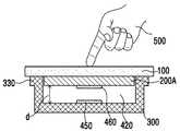
도11e는 도11d에 도시된 터치 입력 장치(1000)에 압력이 인가된 경우의 단면도이다. 기판(300)의 상부면은 노이즈 차폐를 위해 그라운드(ground) 전위를 가질 수 있다. 객체(500)를 통해 커버층(100)의 표면에 압력을 인가하는 경우 커버층(100) 및 디스플레이 패널(200A)은 휘어지거나 눌릴 수 있다. 이에 따라 그라운드 전위면과 압력 센서(450,460) 사이의 거리(d)가 d'로 감소할 수 있다. 이러한 경우, 상기 거리(d)의 감소에 따라 기판(300)의 상부면으로 프린징 정전용량이 흡수되므로 제1센서(450)와 제2센서(460) 사이의 상호 정전용량은 감소할 수 있다. 따라서, 수신센서를 통해 획득되는 감지신호에서 상호 정전용량의 감소량을 획득하여 터치 압력의 크기를 산출할 수 있다.11E is a sectional view when pressure is applied to the
도11e에서는 기판(300)의 상부면이 그라운드 전위, 즉 기준 전위층인 경우에 대하여 설명하였지만, 기준 전위층이 디스플레이 모듈(200) 내부에 배치될 수 있다. 이 때, 객체(500)를 통해 커버층(100)의 표면에 압력을 인가하는 경우 커버층(100) 및 디스플레이 패널(200A)은 휘어지거나 눌릴 수 있다. 이에 따라 디스플레이 모듈(200) 내부에 배치된 기준 전위층과 압력 센서(450,460) 사이의 거리가 변하고, 이에 따라 수신센서를 통해 획득되는 감지신호에서 정전용량 변화량을 획득하여 터치 압력의 크기를 산출할 수 있다.In FIG. 11E, the case where the upper surface of the
본 발명의 실시예에 따른 터치 입력 장치(1000)에서, 디스플레이 패널(200A)은 압력을 인가하는 터치에 따라 휘어지거나 눌릴 수 있다. 실시예에 따라 디스플레이 패널(200A)이 휘어지거나 눌릴 때 가장 큰 변형을 나타내는 위치는 상기 터치 위치와 일치하지 않을 수 있으나, 디스플레이 패널(200A)은 적어도 상기 터치 위치에서 휘어짐을 나타낼 수 있다. 예컨대, 터치 위치가 디스플레이 패널(200A)의 테두리 및 가장자리 등에 근접하는 경우 디스플레이 패널(200A)이 휘어지거나 눌리는 정도가 가장 큰 위치는 터치 위치와 다를 수 있으나, 디스플레이 패널(200A)은 적어도 상기 터치 위치에서 휘어짐 또는 눌림을 나타낼 수 있다.In the
제1센서(450)와 제2센서(460)는 동일한 층에 형성된 형태에 있어서, 도11d 및 도11e에 도시된 제1센서(450)와 제2센서(460) 각각은 도14a에 도시된 바와 같이 마름모꼴 형태의 복수의 센서로 구성될 수 있다. 여기서 복수의 제1센서(450)는 제1축 방향으로 서로 이어진 형태이고, 복수의 제2센서(460)는 제1축 방향과 직교하는 제2축 방향으로 서로 이어진 형태이며, 제1센서(450) 및 제2센서(460) 중 적어도 하나는 각각의 복수의 마름모꼴 형태의 센서가 브릿지를 통해 연결되어 제1센서(450)와 제2센서(460)가 서로 절연된 형태일 수 있다. 또한, 이 때, 도13에 도시된 제1센서(450)와 제2센서(460)는 도14b에 도시된 형태의 센서로 구성될 수 있다.The
이상에서 터치 압력은 제1센서(450)와 제2센서(460) 사이의 상호 정전용량의 변화로부터 검출되는 것이 예시된다. 하지만, 압력 감지부는 제1센서(450)와 제2센서(460) 중 어느 하나의 압력 센서만을 포함하도록 구성될 수 있으며, 이러한 경우 하나의 압력 센서와 그라운드층(기판(300) 또는 디스플레이 모듈(200) 내부에 배치되는 기준 전위층) 사이의 정전용량, 즉 자기 정전용량의 변화를 검출함으로써 터치 압력의 크기를 검출할 수도 있다. 이때, 구동신호는 상기 하나의 압력 센서에 인가되고, 압력 센서와 그라운드층 사이의 자기 정전용량 변화가 상기 압력 센서로부터 감지될 수 있다.It is exemplified that the touch pressure is detected from the change of mutual capacitance between the
예컨대, 도11d에서 압력 센서는 제1센서(450)만을 포함하여 구성될 수 있으며, 이때 기판(300)과 제1센서(450) 사이의 거리 변화에 따라 야기되는 제1센서(450)와 기판(300) 사이의 정전용량 변화로부터 터치 압력의 크기를 검출할 수 있다. 터치 압력이 커짐에 따라 거리(d)가 감소하므로 기판(300)과 제1센서(450) 사이의 정전용량은 터치 압력이 증가할수록 커질 수 있다. 이때, 압력 센서는, 상호 정전용량 변화량 검출 정밀도를 높이기 위해 필요한, 빗살 형태 또는 삼지창 형상을 가질 필요는 없으며, 하나의 판(예컨대, 사각판) 형상을 가질 수도 있으며, 도14d에 도시된 바와 같이 복수의 제1센서(450)가 일정한 간격을 두고 격자 모양으로 배치될 수 있다.For example, in FIG. 11D, the pressure sensor may be configured to include only the
도11f는 압력 센서(450,460)가 스페이서층(420) 내로서 기판(300)의 상부면 및 디스플레이 모듈(200)의 하부면 상에 형성된 경우를 예시한다. 이 때, 도11a에 도시된 바와 같이 압력 감지부가 센서시트로 구성되는 경우, 센서시트는 제1센서(450)를 포함하는 제1센서시트(440-1)와 제2센서(460)를 포함하는 제2센서시트(440-2)로 구성될 수 있다. 이때, 제1센서(450)와 제2센서(460) 중 어느 하나는 기판(300) 상에 형성되고 나머지 하나는 디스플레이 모듈(200)의 하부면 상에 형성될 수 있다. 도11g에서는 제1센서(450)가 기판(300) 상에 형성되고 제2센서(460)가 디스플레이 모듈(200)의 하부면상에 형성된 것을 예시한다.11F illustrates a case in which the
도11g는 압력 센서(450,460)가 스페이서층(420) 내로서 기판(300)의 상부면 및 디스플레이 패널(200A)의 하부면 상에 형성된 경우를 예시한다. 이 때, 제1센서(450)는 디스플레이 패널(200A)의 하부면 상에 형성되고, 제2센서(460)는, 제2센서(460)가 제1절연층(470) 상에 형성되고 제2절연층(471)이 제2센서(460) 상에 형성되는, 센서시트의 형태로 기판(300)의 상부면에 배치될 수 있다.Fig. 11G illustrates a case in which the
객체(500)를 통해 커버층(100)의 표면에 압력을 인가하는 경우 커버층(100) 및 디스플레이 패널(200A)은 휘어지거나 눌릴 수 있다. 이에 따라 제1센서(450)와 제2센서(460) 사이의 거리(d)가 감소할 수 있다. 이러한 경우, 상기 거리(d)의 감소에 따라 제1센서(450)와 제2센서(460) 사이의 상호 정전용량은 증가할 수 있다. 따라서, 수신센서를 통해 획득되는 감지신호에서 상호 정전용량의 증가량을 획득하여 터치 압력의 크기를 산출할 수 있다. 이때, 도11g에서 제1센서(450)와 제2센서(460)는 서로 다른 층에 형성되므로, 제1센서(450) 및 제2센서(460)는 빗살형상 또는 삼지창 형상을 가질 필요는 없으며 제1센서(450) 및 제2센서(460) 중 어느 하나는 하나의 판(예컨대, 사각판) 형상을 가질 수도 있으며, 다른 하나는 도14d에 도시된 바와 같이 복수의 센서가 일정한 간격을 두고 격자 모양으로 배치될 수 있다.When the pressure is applied to the surface of the
상기에서는 도11b에 도시된 바와 같이 압력 센서(450,460)가 디스플레이 패널(200A)의 하면에 직접 형성되는 실시예를 기준으로 설명하였으나 도11a에 도시된 바와 같이 압력 센서(450,460)가 포함된 센서시트(440)가 디스플레이 모듈(200)과 기판(300) 사이에 배치되는 실시예에도 모두 적용 가능하다. 구체적으로, 압력 센서(450,460)가 포함된 센서시트(440)가 디스플레이 모듈(200) 하면에 부착될 수도 있고, 기판(300)의 상면에 부착될 수도 있다.11A, the
이 경우, 기판(300)의 상부면 또한 노이즈 차폐를 위해 그라운드 전위를 가질 수 있다. 도12는 본 발명의 실시예에 따른 센서시트의 단면을 예시한다. 도12의 (a)를 참조하여 설명하면, 압력 센서(450,460)를 포함하는 센서시트(440)가 기판(300) 또는 디스플레이 모듈(200) 상에 부착된 경우의 단면을 예시한다. 이때, 센서시트(440)에서 압력 센서(450,460)는 제1절연층(470)과 제2절연층(471) 사이에 위치하므로, 압력 센서(450,460)가 기판(300) 또는 디스플레이 모듈(200)과 단락되는 것이 방지될 수 있다. 또한, 터치 입력 장치(1000)의 종류 및/또는 구현 방식에 따라, 압력 센서(450,460)가 부착되는 기판(300) 또는 디스플레이 모듈(200)이 그라운드 전위를 나타내지 않거나 약한 그라운드 전위를 나타낼 수 있다. 이러한 경우, 본 발명의 실시예에 따른 터치 입력 장치(1000)는 기판(300) 또는 디스플레이 모듈(200)과 절연층(470) 사이에 그라운드 전극(ground electrode: 미도시)을 더 포함할 수 있다. 실시예에 따라, 그라운드 전극과 기판(300) 또는 디스플레이 모듈(200) 사이에는 또 다른 절연층(미도시)을 더 포함할 수도 있다. 이때, 그라운드 전극(미도시)은 압력 센서인 제1센서(450)와 제2센서(460) 사이에 생성되는 정전용량의 크기가 너무 커지는 것을 방지할 수 있다.In this case, the top surface of the
제1센서(450)와 제2센서(460)는 실시예에 따라 서로 다른 층에 구현되어 센서층을 구성하여도 무방하다. 도12의 (b)는 제1센서(450)와 제2센서(460)가 서로 다른 층에 구현된 경우의 단면을 예시한다. 도12의 (b)에 예시된 바와 같이, 제1센서(450)는 제1절연층(470) 상에 형성되고 제2센서(460)는 제1센서(450) 상에 위치하는 제2절연층(471) 상에 형성될 수 있다. 실시예에 따라, 제2센서(460)는 제3절연층(472)으로 덮일 수 있다. 즉, 센서시트(440)는 제1절연층(470) 내지 제3절연층(472), 제1센서(450) 및 제2센서(460)를 포함하여 구성될 수 있다. 이때, 제1센서(450)와 제2센서(460)는 서로 다른 층에 위치하므로 서로 오버랩(overlap)되도록 구현될 수 있다. 예컨대, 제1센서(450)와 제2센서(460)는 도14c에 도시된 바와 같이, MXN의 구조로 배열된 구동전극(TX)과 수신전극(RX)의 패턴과 유사하게 형성될 수 있다. 이때, M 및 N은 1 이상의 자연수 일 수 있다. 또는, 도14a에 도시된 바와 같이 마름모꼴 형태의 제1센서(450)와 제2센서(460)가 각각 다른 층에 위치할 수도 있다.The
도12의 (c)는 센서시트(440)가 제1센서(450)만을 포함하여 구현된 경우의 단면을 예시한다. 도12의 (c)에 예시된 바와 같이, 제1센서(450)를 포함하는 센서시트(440)는 기판(300) 또는 디스플레이 모듈(200) 상에 배치될 수 있다.FIG. 12C illustrates a cross section of the
도12의 (d)는 제1센서(450)를 포함하는 제1센서시트(440-1)가 기판(300) 상에 부착되고 제2센서(460)를 포함하는 제2센서시트(440-2)가 디스플레이 모듈(200)에 부착된 경우의 단면을 예시한다. 도12의 (d)에 예시된 바와 같이, 제1센서(450)를 포함하는 제1센서시트(440-1)는 기판(300) 상에 배치될 수 있다. 또한, 제2센서(460)를 포함하는 제2센서시트(440-2)는 디스플레이 모듈(200)의 하부면 상에 배치될 수 있다.12D shows a first sensor sheet 440-1 including a
도12의 (a)와 관련하여 설명된 바와 마찬가지로, 압력 센서(450,460)가 부착되는 기판(300) 또는 디스플레이 모듈(200)이 그라운드 전위를 나타내지 않거나 약한 그라운드 전위를 나타내는 경우, 도12의 (a) 내지 (d)에서 센서시트(440)는 기판(300) 또는 디스플레이 모듈(200)과 제1절연층(470, 470-1, 470-2) 사이에 그라운드 전극(미도시)을 더 포함할 수 있다. 이때, 센서시트(440)는 그라운드 전극(미도시)과 기판(300) 또는 디스플레이 모듈(200) 사이에 추가의 절연층(미도시)을 더 포함할 수 있다.12 (a), when the
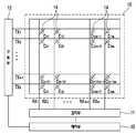
본 발명에 따른 터치 입력 장치(1000)에서 압력 센서(450,460)는 디스플레이 패널(200A)에 직접 형성될 수 있다. 도13a 내지 도13c는 본 발명의 실시예에 따른 터치 입력 장치에서 다양한 디스플레이 패널에 직접 형성된 압력 센서의 실시예를 나타내는 단면도이다.In the
먼저, 도13a는 LCD 패널을 이용하는 디스플레이 패널(200A)에 형성된 압력 센서(450,460)를 도시한다. 구체적으로, 도13a에 도시된 바와 같이, 압력 센서(450,460)가 제2기판층(262) 하면에 형성될 수 있다. 이 때, 압력 센서(450,460)가 제2편광층(272) 하면에 형성될 수도 있다. 터치 입력 장치(1000)에 압력이 인가되면, 상호 정전용량 변화량에 기초하여 터치 압력을 검출하는 경우에는, 구동센서(450)에 구동신호가 인가되고, 압력 센서(450,460)와 이격된 기준 전위층과 압력 센서(450,460)와의 거리 변화에 따라 변화하는 정전용량에 대한 정보를 포함하는 전기적 신호를 수신센서(460)로부터 수신한다. 자기 정전용량 변화량에 기초하여 터치 압력을 검출하는 경우에는, 압력 센서(450,460)에 구동신호가 인가되고, 압력 센서(450,460)와 이격된 기준 전위층과 압력 센서(450,460)와의 거리 변화에 따라 변화하는 정전용량에 대한 정보를 포함하는 전기적 신호를 압력 센서(450,460)로부터 수신한다. 여기서 기준전위층은 기판(300)이거나 디스플레이 패널(200A)과 기판(300) 사이에 배치되며, 디스플레이 패널(200A)을 보호하는 기능을 수행하는 커버일 수 있다.13A shows
다음으로, 도13b는 OLED 패널(특히, AM-OLED 패널)을 이용하는 디스플레이 패널(200A)의 하부면에 형성된 압력 센서(450,460)를 도시한다. 구체적으로, 압력 센서(450,460)가 제2기판층(283) 하면에 형성될 수 있다. 이때, 압력을 검출하는 방법은 도13a에서 설명한 방법과 동일하다.Next, Fig. 13B shows
OLED 패널의 경우, 유기물층(280)에서 빛이 발광하므로, 유기물층(280) 하부에 배치된 제2기판층(283)의 하면에 형성되는 압력 센서(450,460)는 불투명한 물질로 구성될 수 있다. 하지만 이 경우, 디스플레이 패널(200A) 하면에 형성된 압력 센서(450,460)의 패턴이 사용자에게 보일 수 있기 때문에, 압력 센서(450,460)를 제2기판층(283) 하면에 직접 형성시키기 위하여, 제2기판층(283) 하면에 블랙 잉크와 같은 차광층을 도포한 후, 차광층 상에 압력 센서(450,460)를 형성시킬 수 있다.In the case of the OLED panel, since the light is emitted from the
또한, 도13b에서는 제2기판층(283)의 하면에 압력 센서(450,460)가 형성되는 것으로 도시되었지만, 제2기판층(283)의 하부에 제3기판층(미도시)가 배치되고, 제3기판층의 하면에 압력 센서(450,460)가 형성될 수 있다. 특히 디스플레이 패널(200A)이 플렉서블 OLED 패널일 경우, 제1기판층(281), 유기물층(280) 및 제2기판층(283)으로 구성된 디스플레이 패널(200A)이 매우 얇고 잘 휘어지기 때문에, 제2기판층(283)의 하부에 상대적으로 잘 휘어지지 않는 제3기판층을 배치할 수 있다.13B,
다음으로, 도13c는 OLED 패널을 이용하는 디스플레이 패널(200A) 내에 형성된 압력 센서(450,460)를 도시한다. 구체적으로, 압력 센서(450,460)가 제2기판층(283) 상면에 형성될 수 있다. 이때, 압력을 검출하는 방법은 도13a에서 설명한 방법과 동일하다.Next, Fig. 13C shows the
또한, 도13c에서는 OLED 패널을 이용하는 디스플레이 패널(200A)에 대하여 예를 들어 설명하였지만, LCD 패널을 이용하는 디스플레이 패널(200A)의 제2기판층(272) 상면에 압력 센서(450,460)가 형성되는 것도 가능하다.13C, the
또한, 도13a 내지 도13c에서는 압력 센서(450,460)가 제2기판층(272,283)의 상면 또는 하면에 형성되는 것에 대하여 설명하였지만, 압력 센서(450,460)가 제1기판층(261,281)의 상면 또는 하면에 형성되는 것도 가능하다.13A to 13C, the
또한, 도13a 내지 도13c에서는 압력 센서(450,460)가 포함된 압력 감지부가 디스플레이 패널(200A)에 직접 형성되는 것에 대하여 설명하였지만, 압력 감지부가 기판(300)에 직접 형성되고, 전위층이 디스플레이 패널(200A)이거나 디스플레이 패널(200A)과 기판(300) 사이에 배치되며, 디스플레이 패널(200A)을 보호하는 기능을 수행하는 커버일 수 있다.13A to 13C, the pressure sensing unit including the
또한, 도13a 내지 도13c에서는 기준전위층이 압력 감지부의 하부에 배치되는 것에 대하여 설명하였지만, 기준전위층이 디스플레이 패널(200A)의 내부에 배치될 수 있다. 구체적으로, 기준전위층이 디스플레이 패널(200A)의 제1기판층(261,281)의 상면 또는 하면, 또는 제2기판층(262,283)의 상면 또는 하면에 배치될 수 있다.13A to 13C, the reference potential layer is disposed below the pressure sensing portion. However, the reference potential layer may be disposed inside the
본 발명에 따른 터치 입력 장치(1000)에서 정전용량 변화량을 감지하기 위한 압력 센서(450,460)는 도11g에 설명한 바와 같이, 디스플레이 패널(200A)에 직접 형성되는 제1센서(450) 및 센서시트의 형태로 구성된 제2센서(460)로 구성될 수 있다. 구체적으로, 제1센서(450)는 도13a 내지 도13c에 설명한 바와 같이 디스플레이 패널(200A)에 직접 형성되고, 제2센서(460)는 도11g에서 설명한 바와 같이 센서시트의 형태로 구성되어 터치 입력 장치(1000)에 부착될 수 있다.11G, the
본 발명의 실시예에 따른 터치 입력 장치(1000)에서 압력 센서 제어기(1300)와 터치 센서 제어기(1100)가 하나의 IC로 통합되어 구동되는 경우, 통합된 IC의 제어부는 터치 센서 (10)의 스캐닝을 수행함과 동시에 압력 감지부의 스캐닝을 수행하도록 하거나, 또는 통합된 IC의 제어부는 시분할하여 제1시간구간에는 터치 센서(10)의 스캐닝을 수행하도록 하고 제1시간구간과는 다른 제2시간구간에는 압력 감지부의 스캐닝을 수행하도록 제어신호를 생성할 수 있다.When the
이상에서는, 압력 감지부에 포함된 압력 센서(450)가 전극으로 구성되고, 압력 감지부에서 감지하는 전기적 특성으로서 디스플레이 패널(200A)이 휘어짐에 따른 정전용량 변화량을 검출하여 압력의 크기를 검출하는 것에 대하여 설명하였으나, 이에 한정하지 않으며, 압력 감지부에 포함된 압력 센서(450)가 스트레인 게이지로 구성되고, 압력 감지부에서 감지하는 전기적 특성으로서 디스플레이 패널(200A)이 휘어짐에 따라 변하는 압력 센서(450)의 저항값의 변화량을 검출하여 압력의 크기를 검출할 수도 있다.In the above description, the
또한, 이상에서 실시예를 중심으로 설명하였으나 이는 단지 예시일 뿐 본 발명을 한정하는 것이 아니며, 본 발명이 속하는 분야의 통상의 지식을 가진 자라면 본 실시예의 본질적인 특성을 벗어나지 않는 범위에서 이상에 예시되지 않은 여러 가지의 변형과 응용이 가능함을 알 수 있을 것이다. 예를 들어, 실시예에 구체적으로 나타난 각 구성 요소는 변형하여 실시할 수 있는 것이다. 그리고 이러한 변형과 응용에 관계된 차이점들은 첨부된 청구 범위에서 규정하는 본 발명의 범위에 포함되는 것으로 해석되어야 할 것이다.While the present invention has been particularly shown and described with reference to exemplary embodiments thereof, it is clearly understood that the same is by way of illustration and example only and is not to be taken by way of illustration, It can be seen that various modifications and applications are possible. For example, each component specifically shown in the embodiments can be modified and implemented. It is to be understood that all changes and modifications that come within the meaning and range of equivalency of the claims are therefore intended to be embraced therein.
10: 터치 센서11: 감지부
12: 구동부13: 제어부
100: 커버층200: 디스플레이 모듈
300: 기판450, 460: 압력 센서10: touch sensor 11: sensing unit
12: driving unit 13:
100: cover layer 200: display module
300:
Claims (11)
Translated fromKorean상기 디스플레이 영역 하부에 배치되는 디스플레이 패널; 및
상기 디스플레이 패널 하부에 배치되고, 상기 입력 영역에 인접한 위치에 배치되는 압력 감지부;를 포함하고,
상기 압력 감지부는 압력 센서를 포함하고,
상기 커버층에 압력이 인가되면, 상기 커버층 및 상기 디스플레이 패널이 휘어지고,
상기 커버층 및 상기 디스플레이 패널이 휘어짐에 따라 상기 압력 센서의 전기적 특성이 변화하고,
상기 입력 영역에 압력이 인가되면, 상기 압력 센서로부터 출력되는 전기적 특성으로부터 상기 입력 영역에 인가되는 압력의 크기를 검출하는,
터치 입력 장치.A cover layer comprising a display area and an input area;
A display panel disposed below the display area; And
And a pressure sensing unit disposed under the display panel and disposed at a position adjacent to the input area,
Wherein the pressure sensing part includes a pressure sensor,
When a pressure is applied to the cover layer, the cover layer and the display panel are warped,
Wherein the electrical characteristics of the pressure sensor vary as the cover layer and the display panel are warped,
A pressure sensor for detecting a magnitude of a pressure applied to the input region from an electrical characteristic output from the pressure sensor when pressure is applied to the input region,
Touch input device.
상기 디스플레이 영역 하부에 배치되는 디스플레이 패널; 및
상기 디스플레이 패널 하부에 배치되는 압력 감지부;를 포함하고,
상기 압력 감지부는 복수의 압력 센서를 포함하고,
상기 커버층에 압력이 인가되면, 상기 커버층 및 상기 디스플레이 패널이 휘어지고,
상기 커버층 및 상기 디스플레이 패널이 휘어짐에 따라 상기 복수의 압력 센서의 전기적 특성이 변화하고,
상기 디스플레이 영역에 압력이 인가되면 상기 복수의 압력 센서의 전기적 특성으로부터 상기 디스플레이 영역에 인가되는 압력의 크기를 검출하고,
상기 입력 영역에 압력이 인가되면 상기 복수의 압력 센서 중 상기 입력 영역에 인접한 위치에 배치된 하나 이상의 압력 센서로부터 출력되는 전기적 특성으로부터 상기 입력 영역에 인가되는 압력의 크기를 검출하는,
터치 입력 장치.A cover layer comprising a display area and an input area;
A display panel disposed below the display area; And
And a pressure sensing unit disposed under the display panel,
Wherein the pressure sensing unit includes a plurality of pressure sensors,
When a pressure is applied to the cover layer, the cover layer and the display panel are warped,
The electrical characteristics of the plurality of pressure sensors vary as the cover layer and the display panel are warped,
Detecting a magnitude of a pressure applied to the display area from electrical characteristics of the plurality of pressure sensors when a pressure is applied to the display area,
Detecting a magnitude of a pressure applied to the input region from electrical characteristics output from one or more pressure sensors disposed at a position adjacent to the input region among the plurality of pressure sensors when a pressure is applied to the input region,
Touch input device.
상기 커버층은 비-디스플레이 영역을 더 포함하고,
상기 입력 영역은 상기 비-디스플레이 영역 내에 배치되는,
터치 입력 장치.3. The method according to claim 1 or 2,
Wherein the cover layer further comprises a non-display area,
The input area being disposed within the non-display area,
Touch input device.
상기 디스플레이 영역 하부에 배치되는 터치 센서;를 더 포함하고,
상기 터치 센서에 의하여 터치 위치가 감지되지 않고, 상기 검출된 입력 영역에 인가된 압력의 크기가 소정값 이상인 경우, 상기 입력 영역에 대응되는 기능을 실행하는,
터치 입력 장치.The method of claim 3,
And a touch sensor disposed under the display area,
Wherein the controller is configured to perform a function corresponding to the input area when the touch position is not detected by the touch sensor and the magnitude of the pressure applied to the detected input area is equal to or greater than a predetermined value,
Touch input device.
상기 입력 영역 하부에 배치되는 터치 센서;를 더 포함하고,
상기 터치 센서에 의하여 터치 위치가 감지되고, 상기 검출된 입력 영역에 인가된 압력의 크기가 소정값 이상인 경우, 상기 입력 영역에 대응되는 기능을 실행하는,
터치 입력 장치.The method of claim 3,
And a touch sensor disposed under the input area,
A touch position sensing unit for sensing a touch position by the touch sensor and executing a function corresponding to the input area when a magnitude of a pressure applied to the detected input area is equal to or greater than a predetermined value,
Touch input device.
상기 터치 센서는 상기 압력 감지부와 일체로 형성되는,
터치 입력 장치.6. The method of claim 5,
Wherein the touch sensor is formed integrally with the pressure sensing unit,
Touch input device.
상기 입력 영역 하부에 배치되는 사용자 인증 센서;를 더 포함하고,
상기 사용자 인증 센서에 의하여 사용자가 인증되고, 상기 검출된 입력 영역에 인가된 압력의 크기가 소정값 이상인 경우, 상기 입력 영역에 대응되는 기능을 실행하는,
터치 입력 장치.The method of claim 3,
And a user authentication sensor disposed under the input area,
And a function corresponding to the input area when the user is authenticated by the user authentication sensor and the magnitude of the pressure applied to the detected input area is equal to or greater than a predetermined value,
Touch input device.
상기 입력 영역은 상기 디스플레이 영역 내에 배치되는,
터치 입력 장치.3. The method according to claim 1 or 2,
Wherein the input area is disposed within the display area,
Touch input device.
상기 입력 영역 하부에 배치되는 터치 센서;를 더 포함하고,
상기 터치 센서에 의하여 터치 위치가 감지되고, 상기 검출된 입력 영역에 인가된 압력의 크기가 소정값 이상인 경우, 상기 입력 영역에 대응되는 기능을 실행하는,
터치 입력 장치.9. The method of claim 8,
And a touch sensor disposed under the input area,
A touch position sensing unit for sensing a touch position by the touch sensor and executing a function corresponding to the input area when a magnitude of a pressure applied to the detected input area is equal to or greater than a predetermined value,
Touch input device.
상기 입력 영역 하부에 배치되는 사용자 인증 센서;를 더 포함하고,
상기 사용자 인증 센서에 의하여 사용자가 인증되고, 상기 검출된 입력 영역에 인가된 압력의 크기가 소정값 이상인 경우, 상기 입력 영역에 대응되는 기능을 실행하는,
터치 입력 장치.9. The method of claim 8,
And a user authentication sensor disposed under the input area,
And a function corresponding to the input area when the user is authenticated by the user authentication sensor and the magnitude of the pressure applied to the detected input area is equal to or greater than a predetermined value,
Touch input device.
상기 복수의 압력 센서의 전기적 특성의 프로파일에 근거하여 상기 커버층에 인가된 압력이 입력 영역에 인가되었는지를 판단하는,
터치 입력 장치.
3. The method of claim 2,
Determining whether a pressure applied to the cover layer is applied to the input area based on a profile of the electrical characteristics of the plurality of pressure sensors,
Touch input device.
Priority Applications (4)
| Application Number | Priority Date | Filing Date | Title |
|---|---|---|---|
| KR1020170021239AKR101908463B1 (en) | 2017-02-16 | 2017-02-16 | Touch input device |
| CN201810139946.4ACN108446044A (en) | 2017-02-16 | 2018-02-09 | Touch input device |
| PCT/KR2018/001820WO2018151481A1 (en) | 2017-02-16 | 2018-02-12 | Touch input device |
| US15/896,580US20180232092A1 (en) | 2017-02-16 | 2018-02-14 | Touch input device |
Applications Claiming Priority (1)
| Application Number | Priority Date | Filing Date | Title |
|---|---|---|---|
| KR1020170021239AKR101908463B1 (en) | 2017-02-16 | 2017-02-16 | Touch input device |
Related Child Applications (1)
| Application Number | Title | Priority Date | Filing Date |
|---|---|---|---|
| KR1020180120280ADivisionKR102018155B1 (en) | 2018-10-10 | 2018-10-10 | Touch input device |
Publications (2)
| Publication Number | Publication Date |
|---|---|
| KR20180094732A KR20180094732A (en) | 2018-08-24 |
| KR101908463B1true KR101908463B1 (en) | 2018-10-17 |
Family
ID=63106360
Family Applications (1)
| Application Number | Title | Priority Date | Filing Date |
|---|---|---|---|
| KR1020170021239AActiveKR101908463B1 (en) | 2017-02-16 | 2017-02-16 | Touch input device |
Country Status (4)
| Country | Link |
|---|---|
| US (1) | US20180232092A1 (en) |
| KR (1) | KR101908463B1 (en) |
| CN (1) | CN108446044A (en) |
| WO (1) | WO2018151481A1 (en) |
Cited By (1)
| Publication number | Priority date | Publication date | Assignee | Title |
|---|---|---|---|---|
| US11237661B2 (en) | 2019-06-14 | 2022-02-01 | Samsung Display Co., Ltd. | Display module and display device including the same |
Families Citing this family (11)
| Publication number | Priority date | Publication date | Assignee | Title |
|---|---|---|---|---|
| CN108664177B (en)* | 2017-03-29 | 2021-11-12 | 上海耕岩智能科技有限公司 | Method and device for opening application based on fingerprint identification |
| CN107195667B (en)* | 2017-06-30 | 2020-02-21 | 武汉天马微电子有限公司 | A flexible organic light-emitting display panel and electronic device |
| CN108052232B (en)* | 2018-01-03 | 2021-03-19 | 上海天马微电子有限公司 | Display device |
| KR102514729B1 (en)* | 2018-01-18 | 2023-03-29 | 삼성전자주식회사 | Electronic device comprising display including restricted area and operation method of thereof |
| KR102632927B1 (en)* | 2018-04-25 | 2024-02-06 | 삼성디스플레이 주식회사 | Display device |
| KR102555824B1 (en)* | 2018-07-31 | 2023-07-14 | 삼성디스플레이 주식회사 | Display device |
| KR102606925B1 (en)* | 2018-10-08 | 2023-11-27 | 삼성디스플레이 주식회사 | Touch sensor and display device having the same |
| JP2020144802A (en)* | 2019-03-08 | 2020-09-10 | 株式会社ジャパンディスプレイ | Detection device and display |
| KR102866006B1 (en)* | 2019-11-15 | 2025-09-29 | 삼성디스플레이 주식회사 | Electronic device including display panel |
| CN111124178B (en)* | 2019-12-18 | 2023-04-07 | 集创北方(深圳)科技有限公司 | Touch screen initial value setting method, touch screen, display device and electronic equipment |
| KR102839167B1 (en)* | 2021-07-09 | 2025-07-25 | 엘지디스플레이 주식회사 | Flexible sensor and flexible display device |
Citations (1)
| Publication number | Priority date | Publication date | Assignee | Title |
|---|---|---|---|---|
| JP2004287640A (en)* | 2003-03-20 | 2004-10-14 | Hitachi Ltd | Input display device |
Family Cites Families (18)
| Publication number | Priority date | Publication date | Assignee | Title |
|---|---|---|---|---|
| KR20130104598A (en)* | 2012-03-14 | 2013-09-25 | 주식회사 미성포리테크 | Home key apparatus for touch panel device |
| CN102637115A (en)* | 2012-03-19 | 2012-08-15 | 北京百纳威尔科技有限公司 | System, method and mobile terminal device for unlocking touch screens |
| KR20140133274A (en)* | 2013-05-10 | 2014-11-19 | (주)멜파스 | Apparatus for sensing touch and method for sensing touch |
| KR101681305B1 (en)* | 2014-08-01 | 2016-12-02 | 주식회사 하이딥 | Touch input device |
| KR20160083032A (en)* | 2013-11-04 | 2016-07-11 | 퀄컴 인코포레이티드 | User authentication biometrics in mobile devices |
| KR102290892B1 (en)* | 2014-12-12 | 2021-08-19 | 엘지전자 주식회사 | Mobile terminal and method for controlling the same |
| KR101598412B1 (en)* | 2015-02-11 | 2016-02-29 | 주식회사 하이딥 | Electrode sheet and touch input device |
| CN106293290B (en)* | 2015-06-10 | 2023-08-29 | 宸鸿科技(厦门)有限公司 | touch device |
| KR101583765B1 (en)* | 2015-07-27 | 2016-01-08 | 주식회사 하이딥 | Smartphone |
| CN115131834A (en)* | 2015-08-13 | 2022-09-30 | 小米科技有限责任公司 | Mobile device and its screen module, fingerprint collection method, device and electronic device |
| CN105159505B (en)* | 2015-09-29 | 2019-03-15 | Oppo广东移动通信有限公司 | An interface operation method and terminal |
| CN105511679B (en)* | 2015-12-25 | 2019-04-30 | 上海天马微电子有限公司 | glass substrate, touch display screen and touch pressure calculation method |
| CN105468199B (en)* | 2015-12-26 | 2019-01-15 | 宸鸿科技(厦门)有限公司 | A kind of panel with pressure-sensing |
| CN105809141B (en)* | 2016-03-17 | 2018-03-02 | 广东欧珀移动通信有限公司 | Screen component, fingerprint collection and identification method, mobile terminal and electronic device |
| KR101729197B1 (en)* | 2016-04-01 | 2017-05-02 | 엘지디스플레이 주식회사 | Touch display device |
| DK179489B1 (en)* | 2016-06-12 | 2019-01-04 | Apple Inc. | Devices, methods and graphical user interfaces for providing haptic feedback |
| CN106201067A (en)* | 2016-06-29 | 2016-12-07 | 宇龙计算机通信科技(深圳)有限公司 | Contactor control device, display control method, display control unit and terminal |
| EP3514666B1 (en)* | 2016-09-17 | 2020-03-18 | Shenzhen Goodix Technology Co., Ltd. | Touch pressure detection module and device |
- 2017
- 2017-02-16KRKR1020170021239Apatent/KR101908463B1/enactiveActive
- 2018
- 2018-02-09CNCN201810139946.4Apatent/CN108446044A/enactivePending
- 2018-02-12WOPCT/KR2018/001820patent/WO2018151481A1/ennot_activeCeased
- 2018-02-14USUS15/896,580patent/US20180232092A1/ennot_activeAbandoned
Patent Citations (1)
| Publication number | Priority date | Publication date | Assignee | Title |
|---|---|---|---|---|
| JP2004287640A (en)* | 2003-03-20 | 2004-10-14 | Hitachi Ltd | Input display device |
Cited By (1)
| Publication number | Priority date | Publication date | Assignee | Title |
|---|---|---|---|---|
| US11237661B2 (en) | 2019-06-14 | 2022-02-01 | Samsung Display Co., Ltd. | Display module and display device including the same |
Also Published As
| Publication number | Publication date |
|---|---|
| US20180232092A1 (en) | 2018-08-16 |
| CN108446044A (en) | 2018-08-24 |
| WO2018151481A1 (en) | 2018-08-23 |
| KR20180094732A (en) | 2018-08-24 |
Similar Documents
| Publication | Publication Date | Title |
|---|---|---|
| KR101908463B1 (en) | Touch input device | |
| KR101583765B1 (en) | Smartphone | |
| KR101958324B1 (en) | Touch input device | |
| KR101727263B1 (en) | Touch pressure detectable touch input device including display module | |
| KR102245680B1 (en) | Touch input device capable of detecting pressure with display noise compensation applied | |
| KR101958323B1 (en) | Pressure sensing unit and touch input device including the same | |
| KR102044804B1 (en) | Touch input device | |
| KR102044802B1 (en) | Touch input appratus for sensing force which is added at a side of the touch input apparatus | |
| KR102084467B1 (en) | Touch input apparatus | |
| KR101959426B1 (en) | Touch input device including strain gauge | |
| KR102124622B1 (en) | Common mode noise elimination method of touch input apparatus and touch input appratus for the same | |
| KR101880434B1 (en) | Touch input device and method for measuring a capacitance of the same | |
| KR101852413B1 (en) | Pressure sensor detecting mulpiple pressure and touch input device including the same | |
| KR101865303B1 (en) | Touch Input Apparatus | |
| KR101995815B1 (en) | Pressure sensor and touch input device including the same | |
| KR101956295B1 (en) | Touch input device | |
| KR101649986B1 (en) | Touch pressure detectable touch input device including display module | |
| KR101874786B1 (en) | Pressure sensingn unit detecting a plurality of elctrical caracteristics and touch input device including the same | |
| KR101865302B1 (en) | Touch input device | |
| KR102018155B1 (en) | Touch input device | |
| KR101864386B1 (en) | Method for phone connecting in touch input device | |
| KR101811417B1 (en) | Touch pressure detectable touch input device including display module | |
| KR102044800B1 (en) | Touch input device | |
| KR20190029556A (en) | Touch input device including strain gauge | |
| KR20180066582A (en) | Method for inserting memo into object displayed in touch input device |
Legal Events
| Date | Code | Title | Description |
|---|---|---|---|
| A201 | Request for examination | ||
| PA0109 | Patent application | St.27 status event code:A-0-1-A10-A12-nap-PA0109 | |
| PA0201 | Request for examination | St.27 status event code:A-1-2-D10-D11-exm-PA0201 | |
| D13-X000 | Search requested | St.27 status event code:A-1-2-D10-D13-srh-X000 | |
| D14-X000 | Search report completed | St.27 status event code:A-1-2-D10-D14-srh-X000 | |
| E902 | Notification of reason for refusal | ||
| PE0902 | Notice of grounds for rejection | St.27 status event code:A-1-2-D10-D21-exm-PE0902 | |
| P11-X000 | Amendment of application requested | St.27 status event code:A-2-2-P10-P11-nap-X000 | |
| P13-X000 | Application amended | St.27 status event code:A-2-2-P10-P13-nap-X000 | |
| E701 | Decision to grant or registration of patent right | ||
| PE0701 | Decision of registration | St.27 status event code:A-1-2-D10-D22-exm-PE0701 | |
| PG1501 | Laying open of application | St.27 status event code:A-1-1-Q10-Q12-nap-PG1501 | |
| A107 | Divisional application of patent | ||
| GRNT | Written decision to grant | ||
| PA0107 | Divisional application | St.27 status event code:A-0-1-A10-A18-div-PA0107 St.27 status event code:A-0-1-A10-A16-div-PA0107 | |
| PR0701 | Registration of establishment | St.27 status event code:A-2-4-F10-F11-exm-PR0701 | |
| PR1002 | Payment of registration fee | St.27 status event code:A-2-2-U10-U11-oth-PR1002 Fee payment year number:1 | |
| PG1601 | Publication of registration | St.27 status event code:A-4-4-Q10-Q13-nap-PG1601 | |
| P22-X000 | Classification modified | St.27 status event code:A-4-4-P10-P22-nap-X000 | |
| PR1001 | Payment of annual fee | St.27 status event code:A-4-4-U10-U11-oth-PR1001 Fee payment year number:4 | |
| P22-X000 | Classification modified | St.27 status event code:A-4-4-P10-P22-nap-X000 | |
| PN2301 | Change of applicant | St.27 status event code:A-5-5-R10-R11-asn-PN2301 | |
| PN2301 | Change of applicant | St.27 status event code:A-5-5-R10-R14-asn-PN2301 | |
| PR1001 | Payment of annual fee | St.27 status event code:A-4-4-U10-U11-oth-PR1001 Fee payment year number:5 | |
| P22-X000 | Classification modified | St.27 status event code:A-4-4-P10-P22-nap-X000 | |
| R18-X000 | Changes to party contact information recorded | St.27 status event code:A-5-5-R10-R18-oth-X000 | |
| PR1001 | Payment of annual fee | St.27 status event code:A-4-4-U10-U11-oth-PR1001 Fee payment year number:6 | |
| PR1001 | Payment of annual fee | St.27 status event code:A-4-4-U10-U11-oth-PR1001 Fee payment year number:7 | |
| PR1001 | Payment of annual fee | St.27 status event code:A-4-4-U10-U11-oth-PR1001 Fee payment year number:8 |