KR101906591B1 - A dual-mode pixel including emissive and reflective device and dual-mode display using the pixel - Google Patents
A dual-mode pixel including emissive and reflective device and dual-mode display using the pixelDownload PDFInfo
- Publication number
- KR101906591B1 KR101906591B1KR1020120144284AKR20120144284AKR101906591B1KR 101906591 B1KR101906591 B1KR 101906591B1KR 1020120144284 AKR1020120144284 AKR 1020120144284AKR 20120144284 AKR20120144284 AKR 20120144284AKR 101906591 B1KR101906591 B1KR 101906591B1
- Authority
- KR
- South Korea
- Prior art keywords
- self
- optical filter
- type device
- emission type
- delete delete
- Prior art date
- Legal status (The legal status is an assumption and is not a legal conclusion. Google has not performed a legal analysis and makes no representation as to the accuracy of the status listed.)
- Active
Links
- 230000003287optical effectEffects0.000claimsabstractdescription130
- 239000000758substrateSubstances0.000claimsabstractdescription59
- 238000000034methodMethods0.000claimsdescription23
- 238000002347injectionMethods0.000claimsdescription12
- 239000007924injectionSubstances0.000claimsdescription12
- 238000009736wettingMethods0.000claimsdescription12
- 239000004973liquid crystal related substanceSubstances0.000claimsdescription11
- VYPSYNLAJGMNEJ-UHFFFAOYSA-NSilicium dioxideChemical compoundO=[Si]=OVYPSYNLAJGMNEJ-UHFFFAOYSA-N0.000claimsdescription10
- 238000001962electrophoresisMethods0.000claimsdescription8
- 238000010521absorption reactionMethods0.000claimsdescription6
- 239000004038photonic crystalSubstances0.000claimsdescription6
- GWEVSGVZZGPLCZ-UHFFFAOYSA-NTitan oxideChemical compoundO=[Ti]=OGWEVSGVZZGPLCZ-UHFFFAOYSA-N0.000claimsdescription4
- 230000005525hole transportEffects0.000claimsdescription4
- 239000000377silicon dioxideSubstances0.000claimsdescription3
- 239000000203mixtureSubstances0.000claimsdescription2
- OGIDPMRJRNCKJF-UHFFFAOYSA-Ntitanium oxideInorganic materials[Ti]=OOGIDPMRJRNCKJF-UHFFFAOYSA-N0.000claimsdescription2
- 230000009977dual effectEffects0.000abstractdescription33
- 229910052751metalInorganic materials0.000description25
- 239000002184metalSubstances0.000description25
- 239000010408filmSubstances0.000description24
- 239000003921oilSubstances0.000description12
- PXHVJJICTQNCMI-UHFFFAOYSA-NNickelChemical compound[Ni]PXHVJJICTQNCMI-UHFFFAOYSA-N0.000description9
- 239000000463materialSubstances0.000description9
- 238000004088simulationMethods0.000description9
- 230000005540biological transmissionEffects0.000description6
- BQCADISMDOOEFD-UHFFFAOYSA-NSilverChemical compound[Ag]BQCADISMDOOEFD-UHFFFAOYSA-N0.000description5
- 230000005684electric fieldEffects0.000description5
- 239000012530fluidSubstances0.000description5
- 229910052709silverInorganic materials0.000description5
- 239000004332silverSubstances0.000description5
- 229910052782aluminiumInorganic materials0.000description4
- XAGFODPZIPBFFR-UHFFFAOYSA-NaluminiumChemical compound[Al]XAGFODPZIPBFFR-UHFFFAOYSA-N0.000description4
- 239000011651chromiumSubstances0.000description4
- 239000010931goldSubstances0.000description4
- WFKWXMTUELFFGS-UHFFFAOYSA-NtungstenChemical compound[W]WFKWXMTUELFFGS-UHFFFAOYSA-N0.000description4
- 229910052721tungstenInorganic materials0.000description4
- 239000010937tungstenSubstances0.000description4
- KDLHZDBZIXYQEI-UHFFFAOYSA-NPalladiumChemical compound[Pd]KDLHZDBZIXYQEI-UHFFFAOYSA-N0.000description3
- 239000011521glassSubstances0.000description3
- 229910052759nickelInorganic materials0.000description3
- 239000002245particleSubstances0.000description3
- 239000004033plasticSubstances0.000description3
- BASFCYQUMIYNBI-UHFFFAOYSA-NplatinumChemical compound[Pt]BASFCYQUMIYNBI-UHFFFAOYSA-N0.000description3
- 239000010409thin filmSubstances0.000description3
- VYZAMTAEIAYCRO-UHFFFAOYSA-NChromiumChemical compound[Cr]VYZAMTAEIAYCRO-UHFFFAOYSA-N0.000description2
- 230000008901benefitEffects0.000description2
- 239000011575calciumSubstances0.000description2
- 230000008859changeEffects0.000description2
- 229910052804chromiumInorganic materials0.000description2
- 229910017052cobaltInorganic materials0.000description2
- 239000010941cobaltSubstances0.000description2
- GUTLYIVDDKVIGB-UHFFFAOYSA-Ncobalt atomChemical compound[Co]GUTLYIVDDKVIGB-UHFFFAOYSA-N0.000description2
- 239000003086colorantSubstances0.000description2
- PCHJSUWPFVWCPO-UHFFFAOYSA-NgoldChemical compound[Au]PCHJSUWPFVWCPO-UHFFFAOYSA-N0.000description2
- 229910052737goldInorganic materials0.000description2
- AMGQUBHHOARCQH-UHFFFAOYSA-Nindium;oxotinChemical compound[In].[Sn]=OAMGQUBHHOARCQH-UHFFFAOYSA-N0.000description2
- 239000012212insulatorSubstances0.000description2
- 150000002500ionsChemical class0.000description2
- 239000011777magnesiumSubstances0.000description2
- 238000004519manufacturing processMethods0.000description2
- 239000002861polymer materialSubstances0.000description2
- 229920000307polymer substratePolymers0.000description2
- 238000003860storageMethods0.000description2
- GMEQIEASMOFEOC-UHFFFAOYSA-N4-[3,5-bis[4-(4-methoxy-n-(4-methoxyphenyl)anilino)phenyl]phenyl]-n,n-bis(4-methoxyphenyl)anilineChemical compoundC1=CC(OC)=CC=C1N(C=1C=CC(=CC=1)C=1C=C(C=C(C=1)C=1C=CC(=CC=1)N(C=1C=CC(OC)=CC=1)C=1C=CC(OC)=CC=1)C=1C=CC(=CC=1)N(C=1C=CC(OC)=CC=1)C=1C=CC(OC)=CC=1)C1=CC=C(OC)C=C1GMEQIEASMOFEOC-UHFFFAOYSA-N0.000description1
- AWXGSYPUMWKTBR-UHFFFAOYSA-N4-carbazol-9-yl-n,n-bis(4-carbazol-9-ylphenyl)anilineChemical compoundC12=CC=CC=C2C2=CC=CC=C2N1C1=CC=C(N(C=2C=CC(=CC=2)N2C3=CC=CC=C3C3=CC=CC=C32)C=2C=CC(=CC=2)N2C3=CC=CC=C3C3=CC=CC=C32)C=C1AWXGSYPUMWKTBR-UHFFFAOYSA-N0.000description1
- OYPRJOBELJOOCE-UHFFFAOYSA-NCalciumChemical compound[Ca]OYPRJOBELJOOCE-UHFFFAOYSA-N0.000description1
- 101000837344Homo sapiens T-cell leukemia translocation-altered gene proteinProteins0.000description1
- FYYHWMGAXLPEAU-UHFFFAOYSA-NMagnesiumChemical compound[Mg]FYYHWMGAXLPEAU-UHFFFAOYSA-N0.000description1
- 229920000144PEDOT:PSSPolymers0.000description1
- 229910004298SiO 2Inorganic materials0.000description1
- 102100028692T-cell leukemia translocation-altered gene proteinHuman genes0.000description1
- -1TNATAChemical compound0.000description1
- 238000007792additionMethods0.000description1
- 239000000956alloySubstances0.000description1
- 229910045601alloyInorganic materials0.000description1
- 229910052788bariumInorganic materials0.000description1
- DSAJWYNOEDNPEQ-UHFFFAOYSA-Nbarium atomChemical compound[Ba]DSAJWYNOEDNPEQ-UHFFFAOYSA-N0.000description1
- UFVXQDWNSAGPHN-UHFFFAOYSA-Kbis[(2-methylquinolin-8-yl)oxy]-(4-phenylphenoxy)alumaneChemical compound[Al+3].C1=CC=C([O-])C2=NC(C)=CC=C21.C1=CC=C([O-])C2=NC(C)=CC=C21.C1=CC([O-])=CC=C1C1=CC=CC=C1UFVXQDWNSAGPHN-UHFFFAOYSA-K0.000description1
- 229910052791calciumInorganic materials0.000description1
- XCJYREBRNVKWGJ-UHFFFAOYSA-Ncopper(II) phthalocyanineChemical compound[Cu+2].C12=CC=CC=C2C(N=C2[N-]C(C3=CC=CC=C32)=N2)=NC1=NC([C]1C=CC=CC1=1)=NC=1N=C1[C]3C=CC=CC3=C2[N-]1XCJYREBRNVKWGJ-UHFFFAOYSA-N0.000description1
- 239000003989dielectric materialSubstances0.000description1
- 238000002845discolorationMethods0.000description1
- 238000003487electrochemical reactionMethods0.000description1
- 239000003792electrolyteSubstances0.000description1
- 238000006056electrooxidation reactionMethods0.000description1
- 238000005265energy consumptionMethods0.000description1
- 238000005516engineering processMethods0.000description1
- 230000005281excited stateEffects0.000description1
- 230000005283ground stateEffects0.000description1
- RBTKNAXYKSUFRK-UHFFFAOYSA-Nheliogen blueChemical compound[Cu].[N-]1C2=C(C=CC=C3)C3=C1N=C([N-]1)C3=CC=CC=C3C1=NC([N-]1)=C(C=CC=C3)C3=C1N=C([N-]1)C3=CC=CC=C3C1=N2RBTKNAXYKSUFRK-UHFFFAOYSA-N0.000description1
- 238000005286illuminationMethods0.000description1
- 229910052749magnesiumInorganic materials0.000description1
- 239000002086nanomaterialSubstances0.000description1
- 229910052763palladiumInorganic materials0.000description1
- 230000035699permeabilityEffects0.000description1
- 229910052697platinumInorganic materials0.000description1
- 229920000767polyanilinePolymers0.000description1
- 238000011946reduction processMethods0.000description1
- 230000004044responseEffects0.000description1
- 230000002441reversible effectEffects0.000description1
- 235000012239silicon dioxideNutrition0.000description1
- XOLBLPGZBRYERU-UHFFFAOYSA-Ntin dioxideChemical compoundO=[Sn]=OXOLBLPGZBRYERU-UHFFFAOYSA-N0.000description1
- 229910001887tin oxideInorganic materials0.000description1
- YVTHLONGBIQYBO-UHFFFAOYSA-Nzinc indium(3+) oxygen(2-)Chemical compound[O--].[Zn++].[In+3]YVTHLONGBIQYBO-UHFFFAOYSA-N0.000description1
Images


Classifications
- H—ELECTRICITY
- H10—SEMICONDUCTOR DEVICES; ELECTRIC SOLID-STATE DEVICES NOT OTHERWISE PROVIDED FOR
- H10K—ORGANIC ELECTRIC SOLID-STATE DEVICES
- H10K59/00—Integrated devices, or assemblies of multiple devices, comprising at least one organic light-emitting element covered by group H10K50/00
- H10K59/50—OLEDs integrated with light modulating elements, e.g. with electrochromic elements, photochromic elements or liquid crystal elements
- H—ELECTRICITY
- H10—SEMICONDUCTOR DEVICES; ELECTRIC SOLID-STATE DEVICES NOT OTHERWISE PROVIDED FOR
- H10K—ORGANIC ELECTRIC SOLID-STATE DEVICES
- H10K50/00—Organic light-emitting devices
- H10K50/80—Constructional details
- H10K50/85—Arrangements for extracting light from the devices
- H10K50/856—Arrangements for extracting light from the devices comprising reflective means
- H—ELECTRICITY
- H10—SEMICONDUCTOR DEVICES; ELECTRIC SOLID-STATE DEVICES NOT OTHERWISE PROVIDED FOR
- H10K—ORGANIC ELECTRIC SOLID-STATE DEVICES
- H10K2102/00—Constructional details relating to the organic devices covered by this subclass
- H10K2102/301—Details of OLEDs
- H10K2102/302—Details of OLEDs of OLED structures
- H10K2102/3023—Direction of light emission
- H10K2102/3031—Two-side emission, e.g. transparent OLEDs [TOLED]
Landscapes
- Physics & Mathematics (AREA)
- Optics & Photonics (AREA)
- Electroluminescent Light Sources (AREA)
- Devices For Indicating Variable Information By Combining Individual Elements (AREA)
Abstract
Translated fromKoreanDescription
Translated fromKorean본 발명은 자발광형 및 반사형 소자를 포함하는 이중모드 화소 및 이를 이용한 이중모드 디스플레이에 관한 것으로 더욱 상세하게는, 일체화된 자발광형 및 반사형 소자를 포함하는 이중모드 화소 및 이를 이용한 이중모드 디스플레이에 관한 것이다.BACKGROUND OF THE
기존의 디스플레이 기술은 크게 투과형 디스플레이, 자발광형 디스플레이, 반사형 디스플레이로 구분될 수 있다. 투과형 디스플레이는 대표적으로 박막 트랜지스터 액정 표시장치(Thin Film Transistor Liquid Crystal Display; TFTLCD)가 있다. 박막 트랜지스터 액정 표시장치는 뛰어난 화질을 가지고 있어 TV, 모니터, 휴대폰 등에 사용되며, 현재 디스플레이 시장을 주도하고 있다. 하지만 박막 트랜지스터 액정 표시장치는 전력소모가 크고 유연(flexible)하지 못한 단점을 가지고 있다.Conventional display technologies can be largely divided into a transmissive display, a self-emission display, and a reflective display. Typically, a transmissive display is a thin film transistor liquid crystal display (TFT LCD). Thin-film transistor liquid crystal display devices are used in TVs, monitors, mobile phones and the like, and are leading the display market. However, the thin film transistor liquid crystal display device has a disadvantage that it consumes a large amount of power and is not flexible.
자발광형 디스플레이는 대표적으로 유기 발광 소자(Organic Light Emitting Device; OLED)와 플라즈마 디스플레이 패널(Plasma Display Panel; PDP)가 있다. 자발광형 디스플레이는 화소 자체에서 빛을 발광할 수 있기 때문에 응답속도가 빠르고 명암비가 높고, LCD보다 색재현성이 우수항 장점을 가지고 있다. 또한, 유기 발광 소자는 초박형 제작이 가능하여 유연 디스플레이, 투명 디스플레이 등에 적용되고 있다.Organic light emitting devices (OLEDs) and plasma display panels (PDPs) are typical examples of self-emission type displays. Since the self-emission type display can emit light from the pixel itself, the response speed is fast, the contrast ratio is high, and the color reproducibility is superior to that of the LCD. In addition, the organic light emitting device can be manufactured in a very thin form, and is applied to a flexible display, a transparent display, and the like.
반사형 디스플레이는 전기영동 디스플레이(Electrophoretic Display), 전기습윤 디스플레이(Electro Wetting Display), 광결정 디스플레이(Photonic Crystal Display), 마이크로 전자기계 시스템(Microelectromechanical System)등이 있다. 반사형 디스플레이는 햇빛, 조명 등의 외부광을 반사시켜 구동한다. 따라서, 반사형 디스플레이는 주변이 밝을수록 더욱 선명한 화질의 구현이 가능하며 외부광으로 구동되기 때문에 전력소비가 적은 장점이 있다. 하지만, 화질은 투과형 디스플레이와 자발광형 디스플레이보다 나쁘다.Reflective displays include electrophoretic displays, electro-wetting displays, photonic crystal displays, and microelectromechanical systems. The reflective display is driven by reflecting external light such as sunlight and illumination. Therefore, the reflective display has the advantage of being able to realize a clearer image quality as the surrounding area is brighter and the power consumption is reduced because it is driven by external light. However, the picture quality is worse than the transmissive display and the self-luminous display.
투과형 디스플레이 및 자발광형 디스플레이는 실내 또는 어두운 곳에서는 선명한 화질을 가진다. 하지만 야외 또는 밝은 곳에서는 시인성이 떨어지는 단점이 있다. 따라서, 실내 및 실외에서 선명한 화면을 제공하고 에너지 소모량이 적은 디스플레이에 대한 연구가 진행되고 있다.The transmissive display and self-emissive display have clear picture quality in indoor or dark places. However, there is a disadvantage that visibility is reduced in outdoor or bright places. Therefore, research is being conducted on a display that provides a clear image both indoors and outdoors and has a low energy consumption.
본 발명이 해결하고자 하는 과제는 낮은 소비전력과 화질이 보다 향상된 자발광형 및 반사형 소자를 포함하는 이중모드 화소 및 이를 이용한 이중모드 디스플레이에 관한 것이다.The present invention relates to a dual mode pixel including a self light emitting type and a reflective type device with improved power consumption and image quality, and a dual mode display using the dual mode pixel.
본 발명이 해결하고자 하는 과제는 이상에서 언급한 과제에 제한되지 않으며, 언급되지 않은 또 다른 과제들은 아래의 기재로부터 당업자에게 명확하게 이해될 수 있을 것이다.The problems to be solved by the present invention are not limited to the above-mentioned problems, and other problems not mentioned can be clearly understood by those skilled in the art from the following description.
본 발명의 일 실시예에 따른 이중모드 디스플레이는 기판, 및 상기 기판 상의 복수의 세부 화소를 포함하고, 상기 세부 화소 각각은 자발광형 소자, 상기 자발광형 소자의 일측면에 배치된 반사형 광필터, 및 상기 자발광형 소자의 타측면에 배치된 광셔터를 포함한다.A dual mode display according to an embodiment of the present invention includes a substrate and a plurality of sub-pixels on the substrate, wherein each of the sub-pixels includes a self-emission type device, a reflection type optical device disposed on one side of the self- A filter, and an optical shutter disposed on the other side of the self-emission type device.
상기 자발광형 소자는 유기 발광 다이오드일 수 있다.The self-emission type device may be an organic light emitting diode.
상기 유기 발광 다이오드는 기판 상에 차례로 적층된 애노드 전극, 정공 주입층, 정공 수송층, 발광층, 전자 수송층, 전자 주입층, 및 캐소드 전극을 포함할 수 있다.The organic light emitting diode may include an anode electrode, a hole injecting layer, a hole transporting layer, a light emitting layer, an electron transporting layer, an electron injecting layer, and a cathode electrode sequentially stacked on a substrate.
상기 반사형 광필터는 패브리-페로(Fabry-Perot) 광필터, 광결정형 광필터, 흡수방식 광필터, 또는 반사체가 포함된 투과형 광필터일 수 있다.The reflective optical filter may be a transmission type optical filter including a Fabry-Perot optical filter, a photonic crystal optical filter, an absorption type optical filter, or a reflector.
상기 광셔터는 전기영동 방식, 전기습윤 방식, 전기변색 방식, 또는 액정방식으로 구동될 수 있다.The optical shutter may be driven by an electrophoresis method, an electric wetting method, an electrochromic method, or a liquid crystal method.
상기 반사형 광필터와 상기 자발광형 소자 사이에 개재되는 중간 절연막을 더 포함할 수 있다.And an intermediate insulating film interposed between the reflective optical filter and the self-emission type device.
상기 중간 절연막은 실리카, 산화 티타늄 또는 이들의 혼합으로 이루어진 막일 수 있다.The intermediate insulating film may be a film made of silica, titanium oxide, or a mixture thereof.
상기 자발광형 소자는 양면에서 발광할 수 있다.The self-emission type device can emit light on both surfaces.
상기 반사형 광필터는 상기 반사형 광필터 방향으로 발광하는 상기 자발광형 소자의 광을 반사시킬 수 있다.The reflective optical filter may reflect the light of the self-luminous element that emits in the direction of the reflective optical filter.
본 발명의 다른 실시예에 따른 이중모드 디스플레이는 기판, 및 상기 기판 상의 복수의 세부 화소를 포함하고, 상기 세부 화소 각각은 반사형 광필터,A dual mode display according to another embodiment of the present invention includes a substrate and a plurality of sub-pixels on the substrate, each sub-pixel comprising a reflective optical filter,
상기 반사형 광필터 상에 배치된 광셔터, 및 상기 광셔터 상에 배치된 자발광형 소자를 포함한다.An optical shutter disposed on the reflective optical filter, and a self-luminous element disposed on the optical shutter.
상기 자발광형 소자는 유기 발광 다이오드일 수 있다.The self-emission type device may be an organic light emitting diode.
상기 반사형 광필터는 패브리-페로(Fabry-Perot) 광필터, 광결정형 광필터, 흡수방식 광필터, 또는 반사체가 포함된 투과형 광필터일 수 있다.The reflective optical filter may be a transmission type optical filter including a Fabry-Perot optical filter, a photonic crystal optical filter, an absorption type optical filter, or a reflector.
상기 광셔터는 전기영동 방식, 전기습윤 방식, 전기변색 방식, 또는 액정 방식으로 구동될 수 있다.The optical shutter may be driven by an electrophoresis method, an electric wetting method, an electrochromic method, or a liquid crystal method.
본 발명의 또 다른 실시예에 따른 이중모드 디스플레이는 기판, 및 상기 기판 상의 복수의 단위 화소들을 포함하고, 상기 복수의 단위 화소는 반사형 소자 및 상기 반사형 소자 상에 배치된 투명한 자발광형 소자를 포함하되, 상기 반사형 소자는 외부에서 가해지는 전기신호에 따라 다른 색을 반사시키는 광필터 기능을 갖는다.A dual mode display according to another embodiment of the present invention includes a substrate and a plurality of unit pixels on the substrate, the plurality of unit pixels including a reflective element and a transparent self-luminous element The reflection type device has an optical filter function for reflecting different colors according to an electric signal applied from the outside.
상기 자발광형 소자는 유기 발광 다이오드일 수 있다.The self-emission type device may be an organic light emitting diode.
상기 유기 발광 다이오드는 기판 상에 차례로 적층된 애노드 전극, 정공 주입층, 정공 수송층, 발광층, 전자 수송층, 전자 주입층, 및 캐소드 전극을 포함할 수 있다.The organic light emitting diode may include an anode electrode, a hole injecting layer, a hole transporting layer, a light emitting layer, an electron transporting layer, an electron injecting layer, and a cathode electrode sequentially stacked on a substrate.
상기 자발광형 소자는 양면에서 발광할 수 있다.The self-emission type device can emit light on both surfaces.
상기 반사형 소자는 상기 반사형 소자 방향으로 발광하는 상기 자발광 소자의 광을 반사시킬 수 있다.The reflective element may reflect light of the self-luminous element that emits in the direction of the reflective element.
상기 반사형 소자는, MEMS 기반 반사형 소자, 전자습윤 소자 또는 전기변색 소자일 수 있다.The reflective element may be a MEMS-based reflective element, an electro-wetting element, or an electrochromic element.
본 발명의 일 실시예에 따른 자발광형 및 반사형 소자를 포함하는 이중모드 화소는 밝은 곳이나 실외에서는 상기 반사형 광필터를 구동할 수 있고, 어두운 곳이나 실내에서는 상기 자발광형 소자를 구동할 수 있다. 이에 따라, 상기 이중모드 화소를 포함하는 이중모드 디스플레이는 외부 환경에 구애받지 않고 보다 향상된 화질을 제공할 수 있다.The dual mode pixel including the self-emission type and the reflection type device according to an embodiment of the present invention can drive the reflection type optical filter in a bright place or outdoors and can drive the self- can do. Accordingly, the dual mode display including the dual mode pixel can provide improved image quality regardless of the external environment.
본 발명의 일 실시예에 따른 자발광형 및 반사형 소자를 포함하는 이중모드 화소는 상기 반사형 광필터를 제공함으로써 상기 광셔터의 반대 방향으로 방출되는 상기 자발광형 화소의 일부광이 상기 반사형 광필터에 반사되어 외부로 방출될 수 있다. 따라서, 상기 자발광형 소자에 형성된 일부 소실될 수 있는 광이 상기 광셔터 방향으로 형성된 광과 결합하여 이중모드 화소의 전광 특성을 향상시킬 수 있다.A dual mode pixel including a self-emission type and a reflection type device according to an embodiment of the present invention provides the reflective type optical filter so that a part of light of the self-emission type pixel, which is emitted in the direction opposite to the optical shutter, It can be reflected to the type optical filter and emitted to the outside. Accordingly, the partially erasable light formed in the self-light emitting device can be combined with the light formed in the direction of the optical shutter to improve the electro optical characteristics of the dual mode pixel.
도 1은 본 발명의 일 실시예에 따른 이중모드 화소를 포함하는 이중모드 디스플레이를 나타낸 평면도이다.
도 2는 본 발명의 일 실시예에 따른 자발광형 및 반사형 소자를 포함하는 이중모드 화소를 나타낸 단면도이다.
도 3은 본 발명의 다른 실시예에 따른 자발광형 및 반사형 소자를 포함하는 이중모드 화소를 나타낸 단면도이다.
도 4는 본 발명의 또 다른 실시예에 따른 자발광형 및 반사형 소자를 포함하는 이중모드 화소를 나타낸 단면도이다.
도 5는 일반적인 유기 발광 다이오드를 나타낸 단면도이다.
도 6은 본 발명의 일 실시예에 따른 자발광형 및 반사형 소자를 포함한 시뮬레이션 세부 화소를 나타낸 단면도이다.
도 7은 본 발명의 일 실시예에 따른 시뮬레이션 세부 화소를 통해 측정한 반사된 파장 대역을 나타낸 그래프이다.1 is a plan view of a dual mode display including dual mode pixels according to one embodiment of the present invention.
2 is a cross-sectional view illustrating a dual mode pixel including a self-emission type and a reflective type device according to an embodiment of the present invention.
3 is a cross-sectional view illustrating a dual mode pixel including a self-light emitting type and a reflective type device according to another embodiment of the present invention.
4 is a cross-sectional view illustrating a dual mode pixel including a self-emission type and a reflection type device according to another embodiment of the present invention.
5 is a cross-sectional view showing a general organic light emitting diode.
6 is a cross-sectional view illustrating a simulation detailed pixel including a self-emission type and a reflection type device according to an embodiment of the present invention.
7 is a graph illustrating a reflected wavelength band measured through a simulation detailed pixel according to an embodiment of the present invention.
본 발명의 이점 및 특징, 그리고 그것들을 달성하는 방법은 첨부되는 도면과 함께 상세하게 후술되어 있는 실시예를 참조하면 명확해질 것이다. 그러나 본 발명은 이하에서 개시되는 실시예에 한정되는 것이 아니라 서로 다른 다양한 형태로 구현될 수 있으며, 단지 본 실시예는 본 발명의 개시가 완전하도록 하고, 본 발명이 속하는 기술분야에서 통상의 지식을 가진 자에게 발명의 범주를 완전하게 알려주기 위해 제공되는 것이며, 본 발명은 청구항의 범주에 의해 정의될 뿐이다. 명세서 전문에 걸쳐 동일 참조 부호는 동일 구성 요소를 지칭한다.BRIEF DESCRIPTION OF THE DRAWINGS The advantages and features of the present invention, and how to accomplish them, will become apparent by reference to the embodiments described in detail below with reference to the accompanying drawings. The present invention may, however, be embodied in many different forms and should not be construed as being limited to the embodiments set forth herein. Rather, these embodiments are provided so that this disclosure will be thorough and complete, and will fully convey the concept of the invention to those skilled in the art. Is provided to fully convey the scope of the invention to those skilled in the art, and the invention is only defined by the scope of the claims. Like reference numerals refer to like elements throughout the specification.
본 명세서에서 사용된 용어는 실시예들을 설명하기 위한 것이며 본 발명을 제한하고자 하는 것은 아니다. 본 명세서에서, 단수형은 문구에서 특별히 언급하지 않는 한 복수형도 포함한다. 명세서에서 사용되는 '포함한다(comprises)' 및/또는 '포함하는(comprising)'은 언급된 구성요소, 단계, 동작 및/또는 소자는 하나 이상의 다른 구성요소, 단계, 동작 및/또는 소자의 존재 또는 추가를 배제하지 않는다.The terminology used herein is for the purpose of illustrating embodiments and is not intended to be limiting of the present invention. In the present specification, the singular form includes plural forms unless otherwise specified in the specification. As used herein, the terms 'comprises' and / or 'comprising' mean that the stated element, step, operation and / or element does not imply the presence of one or more other elements, steps, operations and / Or additions.
또한, 본 명세서에서 기술하는 실시예들은 본 발명의 이상적인 예시도인 단면도 및/또는 평면도들을 참고하여 설명될 것이다. 도면들에 있어서, 막 및 영역들의 두께는 기술적 내용의 효과적인 설명을 위해 과장된 것이다. 따라서, 제조 기술 및/또는 허용 오차 등에 의해 예시도의 형태가 변형될 수 있다. 따라서, 본 발명의 실시예들은 도시된 특정 형태로 제한되는 것이 아니라 제조 공정에 따라 생성되는 형태의 변화도 포함하는 것이다. 예를 들면, 직각으로 도시된 식각 영역은 라운드지거나 소정 곡률을 가지는 형태일 수 있다. 따라서, 도면에서 예시된 영역들은 개략적인 속성을 가지며, 도면에서 예시된 영역들의 모양은 소자의 영역의 특정 형태를 예시하기 위한 것이며 발명의 범주를 제한하기 위한 것이 아니다.In addition, the embodiments described herein will be described with reference to cross-sectional views and / or plan views, which are ideal illustrations of the present invention. In the drawings, the thicknesses of the films and regions are exaggerated for an effective description of the technical content. Thus, the shape of the illustrations may be modified by manufacturing techniques and / or tolerances. Accordingly, the embodiments of the present invention are not limited to the specific forms shown, but also include changes in the shapes that are generated according to the manufacturing process. For example, the etched area shown at right angles may be rounded or may have a shape with a certain curvature. Thus, the regions illustrated in the figures have schematic attributes, and the shapes of the regions illustrated in the figures are intended to illustrate specific types of regions of the elements and are not intended to limit the scope of the invention.
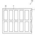
도 1은 본 발명의 일 실시예에 따른 이중모드 화소를 포함하는 이중모드 디스플레이를 나타낸 평면도이다. 도 2는 본 발명의 일 실시예에 따른 자발광형 및 반사형 소자를 포함하는 이중모드 화소를 나타낸 단면도이다.1 is a plan view of a dual mode display including dual mode pixels according to one embodiment of the present invention. 2 is a cross-sectional view illustrating a dual mode pixel including a self-emission type and a reflective type device according to an embodiment of the present invention.
도 1 및 도 2를 참조하면, 자발광형 소자(21)의 일면에 반사형 광필터(23a)가 배치되어 있고, 상기 자발광형 소자(21)의 타면에 광셔터(23b)가 배치되어 있다. 상기 반사형 광필터(23a)와 상기 광셔터(23b)는 하나의 반사형 소자(23)일 수 있다. 이중모드 디스플레이(100)는 다수의 화소(P)로 이루어져 있고, 상기 화소(P)는 다수의 세부 화소들(sub-pixel)(20)로 이루어져 있다. 집적된 상기 자발광형 소자(21), 상기 반사형 광필터(23a), 및 상기 광셔터(23b)는 하나의 세부 화소(sub-pixel)(20)일 수 있다. 상기 세부 화소들(20)은 빨간색(R), 녹색(G), 파란색(B) 각각을 띌 수 있다. 바람직하게, 상기 화소(P)는 흰색(W)을 띄는 세부 화소(20)를 더 포함할 수 있다. 상기 다수의 세부 화소들(20)을 동시에 구동하여 상기 이중모드 디스플레이(100)는 정지된 화면 및 동영상을 구현할 수 있다.1 and 2, a reflection type
상기 반사형 광필터(23a), 상기 자발광형 소자(21), 및 상기 광필터(23b)는 하나의 기판(1) 상에 적층되어 하나의 상기 세부 화소(20)를 형성할 수 있다. 이와 다르게, 상기 반사형 광필터(23a), 상기 자발광형 소자(21), 및 상기 광필터(23b)가 기판 각각에 형성된 후에 적층되어 하나의 상기 세부 화소(20)를 형성할 수 있다. 상기 기판(1)은 유연기판일 수 있다. 상기 유연기판은 예를 들어, 플라스틱, 얇은 유리기판, 또는 금속 기판일 수 있다.The reflection type
상기 자발광형 소자(21)는 유기 발광 다이오드(50; 도5) (Organic Light Emitting diode)일 수 있다. 상기 자발광형 소자(21)는 상기 유기 발광 다이오드에 국한되지 않으며 유연성이 있고 디스플레이 제작이 가능한 자발광형 소자이면 가능하다. 상기 자발광형 소자(21)는 양면에서 특정 색을 발광할 수 있다.The self-
상기 반사형 광필터(23a)는 패브리-페로(Fabry-Perot) 광필터, 광결정형 광필터, 흡수방식 광필터, 또는 반사체가 포함된 투과형 광필터일 수 있다.The reflective
상기 광결정형 광필터는 광의 파장보다 작은 크기의 나노 구조를 이용하여 외부에서 입사되는 광의 파장을 반사 또는 흡수를 제어함으로써 원하는 파장의 광은 투과시키고, 나머지 파장의 광은 반사시킨다.The photonic crystal optical filter transmits light of a desired wavelength and reflects light of the remaining wavelength by controlling reflection or absorption of a wavelength of light incident from the outside using a nanostructure having a size smaller than the wavelength of light.
상기 패브리-페로(Fabry-Perot) 광필터는 두 개의 고 반사율을 가지는 기판들과 상기 기판들 사이에 공진기(cavity)가 삽입된 구조이다. 상기 패브리-페로 광필터에 입사된 광에서 상기 공진층의 다중간섭현상에 의하여 특정 파장대역이 포함된 광은 반사되고 나머지 파장대역들을 포함하는 광은 투과된다.The Fabry-Perot optical filter is a structure in which a cavity is inserted between the substrates having two high reflectances and the substrates. Light having a specific wavelength band is reflected by the multi-interference phenomenon of the resonance layer in the light incident on the Fabry-Perot optical filter, and light including the remaining wavelength bands is transmitted.
상기 흡수방식 광필터는 표시하려는 색의 파장을 반사하고 그 이외 원하지 않는 색의 파장은 흡수한다.The absorption type optical filter reflects the wavelength of the color to be displayed and absorbs the wavelength of the undesired color.
상기 반사체가 포함된 투과형 광필터는 입사된 광 중에서 특정 파장대역 만이 상기 투과형 광필터를 통과하여 상기 반사체에서 반사된다.In the transmission type optical filter including the reflector, only a specific wavelength band of the incident light passes through the transmission type optical filter and is reflected by the reflector.
상기 광셔터(23b)는 전기영동 방식, 전기습윤 방식, 전기변색 방식, 또는 액정방식으로 구동될 수 있다. 상기 광셔터(23b)는 외부광과 상기 자발광형 소자(21)에서 형성된 광을 투과 또는 차단할 수 있다.The
전기영동이란 전하를 띠고 있는 입자가 유체내에 분산된 상태에서 전기장에 의해 이동하는 현상이다. 상기 전기영동 방식은 상기 전기영동을 이용하여 전극에 전압의 인가여부에 따라 상기 입자가 상기 전극 표면에 흡착 또는 비흡착되어 광셔터 기능을 할 수 있다. 상기 전기영동 방식은 약 1 sec(second)의 광 스위치 속도를 가질 수 있다.Electrophoresis is a phenomenon in which charged particles move in an electric field while they are dispersed in a fluid. In the electrophoresis method, the particles may be adsorbed or non-adsorbed to the surface of the electrode depending on whether a voltage is applied to the electrode using the electrophoresis, so that the particles act as an optical shutter. The electrophoresis method may have an optical switch speed of about 1 sec.
전기습윤이란 극성기 및 고 투과성을 가진 도전 유체와 유색의 비극성 오일이 전기장에 의해 이동하는 현상이다. 상기 전기습윤 방식은 전극들 사이에 전압의 인가여부에 따라 상기 유색 비극성 오일이 한쪽으로 수축 또는 비수축되어 광셔터 기능을 할 수 있다. 상기 전기습윤 방식은 약 10 msec(millisecond)의 광 스위치 속도를 가질 수 있다.Electric wetting is a phenomenon in which a polar group and a highly permeable conductive fluid and a colored nonpolar oil move by an electric field. In the electrowetting system, the colored non-polar oil may contract or shrink to one side depending on whether a voltage is applied between the electrodes to function as an optical shutter. The electrowetting scheme may have an optical switch speed of about 10 milliseconds.
전기변색이란 전기화학적 산화나 환원 과정을 통하여 가역적인 광학 특성의 변화를 가지는 형상이다. 전기변색 방식은 약 100 msec(millisecond)의 광 스위치 속도를 가질 수 있다.The electrochromism is a shape having a reversible optical characteristic change through an electrochemical oxidation or reduction process. The electrochromic mode can have an optical switch speed of about 100 msec (millisecond).
액정방식은 염료(dye)가 섞여 있는 액정에 전압을 걸어주면 상기 액정의 방향이 바뀜에 따라 화면이 투명하거나 검게 되는 성질을 이용한다. 액정 방식은 수 msec의 스위칭 속도를 가질 수 있다.In the liquid crystal type, when a voltage is applied to a liquid crystal mixed with a dye, the screen is transparent or black due to a change in the direction of the liquid crystal. The liquid crystal method can have a switching speed of several milliseconds.
상기 광셔터(23b)가 열려있고 상기 자발광형 소자(21)가 구동될 경우, 상기 자발광형 소자(21)에서 형성된 광은 상기 광셔터(23b)를 통하여 외부로 방출하게 된다.When the
상기 자발광형 소자(21)에서 형성된 광 중에서 상기 반사형 광필터(23a) 방향으로 향하는 일부광은 상기 반사형 광필터(23a)에 반사 또는 투과될 수 있다. 상기 반사형 광필터(23a)는 상기 반사형 광필터(23a)의 두께에 따라 상기 외부광에 포함되어 있는 파장을 다르게 반사시킬 수 있다. 이때, 상기 반사형 광필터(23a)에 반사된 파장을 포함하는 광은 고유한 색을 가질 수 있다. 상기 반사된 파장은 하나의 파장 또는 다수의 파장들일 수 있다. 상기 자발광형 소자(21)에서 형성된 상기 일부광이 상기 반사형 광필터(23a)에 반사되기 위하여 상기 반사형 광필터(23a)는 상기 일부광이 가지고 있는 파장대역을 반사시키도록 조절될 수 있다.A part of the light generated by the self-
상기 광셔터(23b)가 열려있고 상기 자발광형 소자(21)가 구동되지 않을 경우, 외부광은 상기 광셔터(23b)와 상기 자발광형 소자(21)를 통과하여 상기 반사형 광필터(23a)에 투과 및 반사될 수 있다. 상기 반사형 광필터(23a)에 반사된 광에 의해서 상기 세부 화소(20)가 구동될 수 있다.When the
상기 광셔터(23b)가 닫혀있을 경우, 비록 상기 자발광형 소자(21)가 구동되더라도 상기 광셔터(23b)가 상기 자발광형 소자(21)의 광을 차단하고 있기 때문에 상기 세부 화소(20)는 검은색을 띌 수 있다.When the
상기 자발광형 소자(21), 광필터(23a), 및 광셔터(23b)가 하나의 상기 세부 화소(20)로 집적되어 있으면 밝은 곳이나 실외에서는 상기 자발광형 소자(21)를 구동하지 않고 상기 반사형 광필터(23a)를 이용하여 상기 세부화소(20)를 구동시키고, 어두운 곳이나 실내에서는 상기 자발광형 소자(21)를 구동시킬 수 있다. 이에 따라, 상기 이중모드 화소(P)를 포함하는 상기 이중모드 디스플레이(100)는 외부 환경에 구애받지 않고 보다 향상된 화질을 제공할 수 있다.If the self-
아울어, 상기 자발광형 소자(21)는 양면에서 광을 형성할 경우 상기 자발광형 소자(21)의 일부광은 상기 광셔터(23b)의 반대 방향으로 방출한다. 다시 말하면, 상기 일부광은 실질적으로 상기 이중모드 디스플레이(100)가 구현될 때 사용되지 못한다. 본 발명의 일 실시예에 따르면, 상기 반사형 광필터(23a)를 제공함으로써 상기 광셔터(23b)의 반대 방향으로 방출되는 상기 자발광형 소자(21)의 광이 상기 반사형 광필터(23a)에 반사되어 외부로 방출될 수 있다. 이에 따라, 상기 자발광형 소자(21)의 양면에서 발광되는 대부분의 광이 외부로 출력될 수 있다. 따라서, 전광특성이 보다 향상된 상기 화소(P)를 갖는 상기 이중모드 디스플레이(100)를 제공할 수 있다.When the self-
또한, 자발광형 소자(21)로 초박형으로 제작이 가능한 유기 발광 다이오드를 사용하여 유연성이 있는 상기 이중모드 디스플레이(100)를 제공할 수 있다.Also, it is possible to provide the
도 3은 본 발명의 다른 실시예에 따른 자발광형 및 반사형 소자를 포함하는 이중모드 화소를 나타낸 단면도이다.3 is a cross-sectional view illustrating a dual mode pixel including a self-light emitting type and a reflective type device according to another embodiment of the present invention.
도 3을 참조하면, 세부 화소(30)는 반사형 소자(33)와 자발광형 소자(31)를 포함할 수 있다. 상기 반사형 소자(33) 상에 상기 자발광형 소자(31)가 배치될 수 있다. 상기 반사형 소자(33)는 반사형 광필터(33a)와 광셔터(33b)를 포함할 수 있다. 상기 광셔터(33b)는 상기 자발광형 소자(31)와 상기 반사형 광필터(33b) 사이에 개재될 수 있다. 상기 자발광형 소자(31)는 양면에서 광을 형성할 수 있다.Referring to FIG. 3, the
상기 광셔터(33b)가 닫혀 있고 상기 자발광형 소자(31)가 구동될 때, 상기 자발광형 소자(31)에서 발생되는 일부광은 외부로 직접적으로 출력될 수 있다. 그러나 상기 광셔터(33b) 방향으로 형성된 일부광은 상기 광셔터(33b)가 닫혀있기 때문에 상기 일부광이 상기 반사형 광필터(33a)에 반사되지 못하여 외부로 방출될 수 없다.When the
상기 광셔터(33b)가 열려 있고 상기 자발광형 소자(31)가 구동될 경우, 상기 자발광형 소자(31)에서 발생되는 일부광은 외부로 직접적으로 방출될 수 있고, 상기 광셔터(33b) 방향으로 형성된 일부광은 상기 반사형 광필터(33a)에 반사된 후 상기 광셔터(33b)과 상기 자발광형 소자(31)를 관통하여 외부로 방출될 수 있다. 이에 따라, 양면에 형성된 상기 자발광형 소자(31)의 광은 외부로 방출될 수 있다.When the
상기 광셔터(31)가 열려 있고 상기 자발광형 소자(31)가 구동되지 않을 경우, 외부광은 상기 자발광형 소자(31)와 상기 광셔터(33b)를 통과하여 상기 반사형 광필터(33a)에 투과 또는 반사될 수 있다. 상기 반사형 광필터(33a)에 반사된 일부광에 의해서 세부 화소(30)는 구동될 수 있다.When the
도 4는 본 발명의 또 다른 실시예에 따른 자발광형 및 반사형 소자를 포함하는 이중모드 화소를 나타낸 단면도이다.4 is a cross-sectional view illustrating a dual mode pixel including a self-emission type and a reflection type device according to another embodiment of the present invention.
도 4를 참조하면, 세부 화소(40)는 반사형 소자(41)과 자발광형 소자(43)를 포함한다. 상기 자발광형 소자(43)는 상기 반사형 소자(41) 상에 배치될 수 있다.Referring to FIG. 4, the
상기 반사형 소자(41)는 상기 반사형 소자(41)에 가해지는 전기신호에 따라 다른 색을 반사시키는 광필터 기능을 가질 수 있다. 예를 들어, 상기 반사형 소자(41)에 전압이 인가될 때 상기 반사형 소자(41)에서 반사되는 색과 상기 반사형 소자(41)에 전압이 인가되지 않을 때 상기 반사형 소자(41)에서 반사되는 색이 다를 수 있다. 상기 반사형 소자(41)는 MEMS 기반 반사형 소자, 전자습윤 소자 및 전기변색 소자일 수 있다.The reflective element 41 may have an optical filter function to reflect a different color according to an electrical signal applied to the reflective element 41. For example, when a voltage is applied to the reflective element 41, the color reflected by the reflective element 41 and the reflective element 41 when no voltage is applied to the reflective element 41, May be different in color. The reflective element 41 may be a MEMS-based reflective element, an electro-wetting element, and an electrochromic element.
상기 MEMS 기반 반사형 소자는 패브리-페로(Fabry-perot) 광필터일 수 있다. 상기 패브리-페로(Fabry-perot) 광필터는 두 개의 금속 기판들과 상기 금속 기판들 사이에 배치되는 유전체 기판을 포함할 수 있다. 상기 유전체 기판은 하나의 상기 금속 기판의 접촉되어 있고, 다른 상기 금속 기판과 이격되어 배치될 수 있다. 상기 금속 기판들 사이의 이격 거리는 상기 MEMS 기반 반사형 소자에 인가하는 전기신호에 따라 달라질 수 있다. 그리고, 상기 금속 기판들 사이의 이격 거리가 달라짐으로 인하여 상기 유전체 기판은 이격되어 있는 상기 금속 기판과 접촉될 수 있다. 상기 MEMS 기반 반사형 소자의 스위칭 속도는 약 수십 ?ec일 수 있다.The MEMS-based reflective element may be a Fabry-Perot optical filter. The Fabry-Perot optical filter may include two metal substrates and a dielectric substrate disposed between the metal substrates. The dielectric substrate is in contact with one of the metal substrates and may be disposed apart from the other metal substrate. The spacing between the metal substrates may vary depending on the electrical signal applied to the MEMS-based reflective element. The dielectric substrate may be in contact with the spaced apart metal substrate due to the difference in distance between the metal substrates. The switching speed of the MEMS based reflective type device may be about several tens of ec.
상기 금속 기판들 사이의 이격 거리에 따라 상기 MEMS 기반 반사형 소자에서 반사되는 색이 달라질 수 있다. 예를 들어, 상기 MEMS 기반 반사형 소자에 전압이 인가될 때, 상기 금속 기판들 사이의 이격 거리에서 반사되는 색은 빨강색(Red) 파랑색(Blue) 초록색(Green) 및 흰색(White) 중 어느 하나일 수 있다. 상기 MEMS 기반 반사형 소자에 전압이 인가되지 않을 때 상기 금속 기판들 사이의 이격 거리에서 반사되는 색은 검은색일 수 있다.The color reflected from the MEMS-based reflective type device may vary depending on the distance between the metal substrates. For example, when a voltage is applied to the MEMS-based reflection type device, the colors reflected at the distance between the metal substrates are red, blue, green, and white, It can be either. When the voltage is not applied to the MEMS-based reflection type device, the color reflected at the distance between the metal substrates may be black.
상기 금속 기판들은 은(Ag), 알루미늄(Al), 금(Au), 코발트(Co), 크롬(Cr), 니켈(Ni), 및 텅스텐(W) 중 어느 하나의 원소를 포함할 수 있다. 상기 유전체 기판은 투명한 유전체 물질로 이루어질 수 있다. 상기 유전체 기판은 예를 들어, 이산화 규소(SiO2)기판, 또는 이산화 티타늄(TiO2)기판일 수 있다.The metal substrates may include any one of silver (Ag), aluminum (Al), gold (Au), cobalt (Co), chromium (Cr), nickel (Ni), and tungsten (W). The dielectric substrate may be made of a transparent dielectric material. The dielectric substrate may be, for example, a silicon dioxide (SiO2 ) substrate or a titanium dioxide (TiO2 ) substrate.
상기 전기습윤 소자는 두 장의 기판들과 상기 기판들 사이에 전기장에 의해 외부광의 투과, 및 반사를 가역적으로 제어하는 전기 습윤 요소(electro-wetting element)를 포함한다. 상기 전기 습윤 요소는 극성기 및 고 투과성을 가진 무색의 도전 유체와 유색의 비극성 오일을 포함할 수 있다. 상기 전기습윤 소자의 스위칭 속도는 약 10msec 이하일 수 있다.The electro-wetting element includes an electro-wetting element between the two substrates and the substrates for reversibly controlling the transmission and reflection of external light by an electric field. The electrowetting element may comprise a polar group and a colorless conductive fluid with high permeability and a colored nonpolar oil. The switching speed of the electrowetting device may be about 10 msec or less.
상기 전기습윤 소자의 구동원리는 다음과 같다. 상기 기판들 상에 배치되고 서로 마주보고 있는 두 장의 전극들에 전압을 인가한다. 인가된 전극들에 의하여 상기 두 기판 사이에 전기장이 형성되고, 상기 전기장에 의하여 도전성을 갖는 상기 무색의 유체는 상기 기판들 표면에 형성된다. 그러므로, 상기 전자습윤 소자는 흰색을 띌 수 있다. 이와 달리, 상기 두 전극들에 전압이 인가되지 않으면 상기 기판들 표면에 유색의 비극성 오일이 형성된다. 그러므로, 외부광이 상기 유색의 비극성 오일에 반사되어 상기 전자습윤 소자는 상기 비극성 오일의 색을 띌 수 있다.The driving principle of the electrowetting element is as follows. A voltage is applied to the two electrodes disposed on the substrates and facing each other. An electric field is formed between the two substrates by the applied electrodes, and the colorless fluid having conductivity by the electric field is formed on the surfaces of the substrates. Therefore, the electro-wetting element may be white. Alternatively, when no voltage is applied to the two electrodes, a colored non-polar oil is formed on the surfaces of the substrates. Therefore, external light is reflected to the colored non-polar oil so that the electro-wetting element can color the non-polar oil.
상기 전기변색 소자는 전기신호를 인가하여 화학 반응을 조절함으로써 전기변색 물질의 색을 조절하는 표시소자이다. 상기 전기변색 소자의 스위칭 속도는 약 100msec일 수 있다.The electrochromic device is a display device for controlling the color of an electrochromic material by controlling an electrochemical reaction by applying an electric signal. The switching speed of the electrochromic device may be about 100 msec.
상기 전기변색 소자의 구동원리는 다음과 같다. 서로 이격되어 있는 상기 투명 기판들 사이에 서로 마주보고 있는 두 개의 전극들을 포함한다. 두 개의 상기 전극들 사이에 차례로 전기 변색층, 전해질층, 및 이온 스토리지(ion storage)가 개재될 수 있다. 상기 전극들 사이에 전압이 인가되어 상기 전기 변색층에서 상기 이온 스토리지로 전류가 흐르면 상기 전기 변색층이 착색될 수 있고, 반대 방향으로 전류가 흐르면 상기 전기 변색층에서 탈색이 일어날 수 있다.The driving principle of the electrochromic device is as follows. And two electrodes facing each other between the transparent substrates spaced apart from each other. An electrochromic layer, an electrolyte layer, and an ion storage may be interposed between the two electrodes. When a voltage is applied between the electrodes, a current flows from the electrochromic layer to the ion storage layer, the electrochromic layer may be colored, and if an electric current flows in the opposite direction, discoloration may occur in the electrochromic layer.
상기 자발광형 소자(43)는 유기 발광 다이오드(Organic Light Emitting diode)(50)일 수 있다. 상기 자발광형 소자(43)는 상기 유기 발광 다이오드에 국한되지 않으며 유연성이 있고 디스플레이 제작이 가능한 자발광형 소자이면 가능하다. 상기 자발광형 소자(43)는 양면에서 발광할 수 있고 특정 색을 발광할 수 있다.The self-
상기 자발광형 소자(43)가 구동되지 않을 경우, 외부광은 상기 자발광형 소자(43)를 통과하여 상기 반사형 소자(41)의 구동여부에 따라 투과 및 반사될 수 있다. 예를 들어, 상기 반사형 소자(41)가 전기습윤 소자이고 상기 전기습윤 소자가 구동될 경우, 상기 외부광은 무색의 도전 유체를 투과할 수 있다. 이에 따라, 상기 세부 화소(40)는 흰색을 띌 수 있다. 이와 달리, 상기 전기습윤 소자가 구동되지 않을 경우, 상기 외부광은 상기 유색의 비극성 오일에 반사될 수 있다. 따라서, 상기 세부 화소(40)는 상기 유색의 비극성 오일의 색을 띌 수 있다.When the self-
상기 자발광형 소자(43)가 구동될 경우, 상기 자발광형 소자(43)에서 발생된 광 중에서 일부광은 외부로 방출될 수 있고, 다른 일부광은 상기 반사형 소자(41)로 입사될 수 있다. 상기 반사형 소자(41)로 입사된 상기 일부광은 상기 반사형 소자(41)의 구동여부에 따라서 반사 또는 투과될 수 있다. 예를 들어, 상기 반사형 소자(41)가 전기습윤 소자이고 상기 전자습윤 소자가 구동되지 않을 경우, 상기 다른 일부광은 상기 유색의 비극성 오일에 반사될 수 있다. 이때, 상기 다른 일부광이 갖고 있는 파장은 상기 비극성 오일이 갖고 있는 색의 파장과 같을 수 있다. 상기 비극성 오일에 반사되는 광은 하나의 파장 또는 다수의 파장들을 가질 수 있고, 상기 광은 상기 비극성 오일이 갖고 있는 색을 띌 수 있다.When the self-
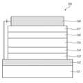
도 5는 일반적인 유기 발광 다이오드를 나타낸 단면도이다.5 is a cross-sectional view showing a general organic light emitting diode.
도 5를 참조하면, 상기 유기 발광 다이오드(50)는 기판(51) 상에 차례로 적층된 애노드 전극(52), 정공주입층(53), 정공수송층(54), 발광층(55), 전자수송층(56), 전자주입층(57), 및 캐소드 전극(58)을 포함할 수 있다.5, the organic
상기 기판(51)은 광 투과 물질로 이루어질 수 있다. 상기 기판(51)은 예를 들어, 유리 기판, 플라스틱 기판, 또는 고분자 기판과 같은 투명한 기판일 수 있다.The
상기 애노드 전극(52)은 투명전극 또는 반사전극으로 형성될 수 있다. 상기 애노드 전극(52)이 투명전극인 경우 예를 들어, 인듐 주석 옥사이드(ITO), 인듐 아연 옥사이드(IZO), 또는 주석 옥사이드을 사용하여 형성할 수 있다. 상기 애노드 전극(52)이 반사전극인 경우 예를 들어, 은(Ag), 알루미늄(Al), 니켈(Ni), 백금(Pt), 또는 팔라듐(Pd)을 사용하여 형성할 수 있다. 본 발명의 실시예에서 상기 애노드 전극(52)은 투명전극으로 사용될 수 있다.The
상기 정공주입층(53)은 상기 애노드 전극(52)에 형성된 정공이 상기 발광층(55)으로의 주입을 용이하게 할 수 있다. 상기 정공주입층(53)은 예를 들어, CuPc(copper phthalocyanine), TNATA, TCTA, TDAPB와 같은 저분자 재료와 PANI, PEDOT:PSS와 같은 고분자 재료를 사용하여 형성될 수 있다.The
상기 정공수송층(54)은 NPB, TPD, s-TAD, MTTADATA등의 저분자 재료와 PVK, BFE, TFB와 같은 고분자 재료를 사용하여 형성될 수 있다.The
상기 발광층(55)은 빛을 방출하는 영역이다. 상기 발광층(55)은 Alq3로 형성될 수 있다.The
상기 전자수송층(56)은 예를 들어, PBD, TAZ, 또는 spiro-PBD와 같은 고분자 재료와 Alq3, BAlq, 또는 SAlq와 같은 저분자 재료를 사용하여 형성될 수 있다.The
상기 전자주입층(57)은 상기 캐소드 전극(58)에서 형성된 전자가 상기 발광층(55)으로의 주입을 용이하게 할 수 있다. 상기 전자수송층(56)은 예를 들어, Alq3, 갈륨 혼합물(Ga complex), 또는 PBD를 사용하여 형성될 수 있다.The
상기 캐소드 전극(58)은 마그네슘(Mg), 칼슘(Ca), 알루미늄(Al), 은(Ag), 또는 바륨(Ba) 또는 이들의 합금으로 형성될 수 있다. 상기 캐소드 전극(58)은 광을 투과할 수 있을 정도로 얇게 형성될 수 있다.The
상기 유기발광 다이오드(50)는 상기 애노드 전극(52)과 상기 캐소드 전극(58)에 전압을 인가하면 상기 애노드 전극(52)에 정공이 형성되고 상기 캐소드 전극(58)에 전자가 형성된다. 상기 정공은 상기 정공 주입층(53)과 상기 정공 수송층(54)을 거쳐서 상기 발광층(55)으로 주입되고, 상기 전자는 상기 전자 주입층(57)과 상기 전자 수송층(56)을 거쳐서 상기 발광층(55)으로 주입된다. 상기 정공과 상기 전자는 상기 발광층(55)에서 재결합하여 엑시톤(exciton)을 생성하고, 상기 엑시톤이 여기 상태에서 기저 상태로 전이되면서 광이 형성하게 된다.When the organic
도 6은 본 발명의 일 실시예에 따른 자발광형 및 반사형 소자를 포함한 시뮬레이션 세부 화소를 나타낸 단면도이다. 도 7은 본 발명의 일 실시예에 따른 시뮬레이션 세부 화소를 통해 측정한 반사된 파장 대역을 나타낸 그래프이다.6 is a cross-sectional view illustrating a simulation detailed pixel including a self-emission type and a reflection type device according to an embodiment of the present invention. 7 is a graph illustrating a reflected wavelength band measured through a simulation detailed pixel according to an embodiment of the present invention.
도 6을 참조하면, 시뮬레이션 세부 화소(60)는 반사형 광필터(62) 상에 자발광형 소자(61)와 기판(67)이 차례로 배치되어 있다. 상기 반사형 광필터(62)와 상기 자발광형 소자(61) 사이에 중간 절연막(65)이 개재될 수 있다.Referring to Fig. 6, the simulation
상기 기판(67)은 광 투과 물질로 이루어질 수 있다. 상기 기판(67)은 예를 들어, 유리 기판, 플라스틱 기판, 또는 고분자 기판과 같은 투명한 기판일 수 있다.The
상기 반사형 광필터(62)는 패브리-페로(Fabry-perot) 광필터이다. 상기 패브피-페로(Fabry-perot) 광필터는 차례로 적층된 제 1 금속막(62a), 광필터 절연막(62b), 및 제 2 금속막(62c)을 포함할 수 있다. 상기 제 1 및 제 2 금속막(62a, 62c)은 예를 들어, 은(Ag), 알루미늄(Al), 금(Au), 코발트(Co), 크롬(Cr), 니켈(Ni), 및 텅스텐(W) 중 어느 하나의 원소를 포함할 수 있다. 상기 광필터 절연막(62b)은 절연체이고 투명한 광학 물질일 수 있다. 상기 광필터 절연막(62b)은 예를 들어, 실리카(SiO2), 산화 티타늄(TiO2) 또는 이들의 혼합으로 이루어질 수 있다. 본 발명의 일 실시예에서 따르면, 상기 제 1 금속막(62a)은 은(Ag)일 수 있고, 상기 광필터 절연막(62b)은 실리카(SiO2)를 포함할 수 있고, 상기 제 2 금속막(62c)은 텅스텐(W)을 포함할 수 있다.The reflective
상기 패브리-페로(Fabry-Perot) 광필터는 상기 제 1 금속막(62a)과 상기 제 2 금속막(62c)의 공진현상을 이용하여 원하는 파장이 포함된 광을 반사시킬 수 있다. 상기 광필터 절연막(62b)의 두께변화에 따라 상기 패브리-페로 광필터에 반사되는 파장이 다를 수 있다.The Fabry-Perot optical filter can reflect light having a desired wavelength using the resonance phenomenon between the
상기 자발광형 소자(61)는 유기 발광 다이오드이다. 상기 유기 발광 다이오드는 차례로 적층된 캐소드 전극(61a), 발광층(61b), 및 애노드 전극(61c)를 포함할 수 있다. 도 6에서 도시되지는 않았지만 상기 발광층(61b)은 도 5에서 설명된 정공 주입층(53), 정공 수송층(54), 전자 수송층(56), 및 전자 주입층(57)을 포함할 수 있다.The self-
본 발명의 일 실시예에 따르면, 상기 캐소드 전극(61a)은 은(Ag)일 수 있고, 상기 애노드 전극(61c)은 인듐 주석 산화막(ITO)일 수 있다. 상기 캐소드 전극(61a)은 최대한 얇게 형성될 수 있다. 왜냐하면 상기 자발광형 소자(61)로 들어오는 외부광 또는 상기 반사형 광필터(62)에서 반사되어 상기 자발광형 소자(61)를 통과하는 반사광이 상기 캐소드 전극(61a)에서 최소한의 광손실을 갖도록 하기 위함이다.According to an embodiment of the present invention, the
상기 중간 절연막(65)의 일면은 상기 반사형 광필터(62)의 상기 제 2 금속막(62c)과 접촉될 수 있고, 상기 중간 절연막(65)의 타면은 상기 자발광형 소자(61)의 상기 캐소드 전극(61a)과 접촉될 수 있다. 상기 중간 절연막(65)은 상기 제 2 금속막(62c)과 상기 캐소드 전극(61a) 사이를 전기적으로 절연시켜줄 수 있다. 상기 중간 절연막(65)은 절연체이고, 투명한 광학 물질을 포함할 수 있다. 상기 중간 절연막(65)은 실리카(SiO2)를 포함할 수 있고, 상기 제 2 금속막(62c)은 텅스텐(W)을 포함할 수 있다. 본 발명의 일 실시예에 따르면, 상기 중간 절연막(65)은 실리카(SiO2)이다.One surface of the intermediate insulating
도 7을 참조하면, 상기 캐소드 전극(61a), 상기 애노드 전극(61c), 상기 제 1 금속막(62a) 및 상기 제 2 금속막(62c) 및 상기 중간 절연막(65)은 약 2nm, 약 70nm, 약 80nm, 약 8nm, 및 약 10nm의 고정적인 두께를 가진다. 상기 광필터 절연막(62b)은 약 200nm, 약 340nm, 또는 약 305nm의 두께를 가진다. 상기 발광층(61b)의 두께는 약 280nm, 약 220nm, 또는 약 180nm 두께를 가진다. 상기 발광층(61b) 및 상기 광필터 절연막(62b)의 두께변화에 따라 상기 시뮬레이션 세부 화소(60)에서 발광하는 색이 다를 수 있다. 바람직하게는, 상기 시뮬레이션 세부 화소(60)에 방출되는 광이 가지고 있는 반사파장이 다를 수 있다. 상기 반사형 광필터(62)는 관측각에 따라 반사율의 값이 최대인 파장대역이 다를 수 있다. 본 발명의 일 실시예에서의 관측각은 30도이다.7, the
그 결과, 상기 시뮬레이션 세부 화소(60)는 빨간색(R), 녹색(G), 파란색(B)을 각각 발광할 때 약 80% 이상의 반사율을 가질 수 있다. 결과적으로, 상기 시뮬레이션 세부 화소(60)는 선명한 색을 구현할 수 있다. 따라서, 상기 세부 화소(60)를 이중모드 디스플레이에 적용할 경우 외부 환경에 영향을 받지 않고 선명한 화질을 구현할 수 있다.As a result, the simulation
이상, 첨부된 도면을 참조하여 본 발명의 실시예를 설명하였지만, 본 발명이 속하는 기술분야에서 통상의 지식을 가진 자는 본 발명이 그 기술적 사상이나 필수적인 특징을 변경하지 않고서 다른 구체적인 형태로 실시될 수 있다는 것을 이해할 수 있을 것이다. 그러므로 이상에서 기술한 실시예에는 모든 면에서 예시적인 것이며 한정적이 아닌 것으로 이해해야만 한다.
While the present invention has been described in connection with what is presently considered to be practical exemplary embodiments, it is to be understood that the invention is not limited to the disclosed embodiments, but, on the contrary, It will be understood. It is therefore to be understood that the above-described embodiments are illustrative and not restrictive in every respect.
20, 30, 40: 세부 화소
21, 31, 43: 자발광형 소자
23, 33, 41: 반사형 소자
23a, 33a: 반사형 광필터
23b, 33b: 광셔터
50: 유기발광 다이오드
51: 기판
52: 애노드 전극
53: 정공 주입층
54: 정공 수송층
55: 발광층
56: 전자 수송층
57: 전자 주입층
58: 캐소드 전극
100: 이중모드 디스플레이20, 30, 40: Detail pixel
21, 31, 43: self-emission type device
23, 33, 41: reflection type device
23a, 33a: a reflection type optical filter
23b, 33b: optical shutter
50: organic light emitting diode
51: substrate
52: anode electrode
53: Hole injection layer
54: hole transport layer
55: light emitting layer
56: electron transport layer
57: electron injection layer
58: cathode electrode
100: Dual mode display
Claims (19)
Translated fromKorean상기 기판 상의 복수의 세부 화소를 포함하고,
상기 세부 화소 각각은
자발광형 소자;
상기 자발광형 소자의 일면에 배치된 반사형 광필터;
상기 반사형 광필터와 상기 자발광형 소자 사이에 개재된 중간 절연막; 및
상기 자발광형 소자의 타면에 배치된 광셔터를 포함하되,
상기 중간 절연막은 투명한 막인 이중모드 디스플레이.Board; And
A plurality of sub-pixels on the substrate,
Each of the sub-
A self-luminous element;
A reflective optical filter disposed on one surface of the self-emission type device;
An intermediate insulating film interposed between the reflection type optical filter and the self-emission type device; And
And an optical shutter disposed on the other surface of the self-luminous element,
Wherein the intermediate insulating film is a transparent film.
상기 자발광형 소자는 유기 발광 다이오드인 이중모드 디스플레이.The method according to claim 1,
Wherein the self-emission type device is an organic light-emitting diode.
상기 유기 발광 다이오드는 기판 상에 차례로 적층된 애노드 전극, 정공 주입층, 정공 수송층, 발광층, 전자 수송층, 전자 주입층, 및 캐소드 전극을 포함하는 이중모드 디스플레이.3. The method of claim 2,
Wherein the organic light emitting diode comprises an anode electrode, a hole injection layer, a hole transport layer, a light emitting layer, an electron transport layer, an electron injection layer, and a cathode electrode sequentially stacked on a substrate.
상기 반사형 광필터는 패브리-페로(Fabry-Perot) 광필터, 광결정형 광필터, 흡수방식 광필터, 또는 반사체가 포함된 투과형 광필터인 이중모드 디스플레이.The method according to claim 1,
Wherein the reflective optical filter is a transmissive optical filter including a Fabry-Perot optical filter, a photonic crystal optical filter, an absorption type optical filter, or a reflector.
상기 광셔터는 전기영동 방식, 전기습윤 방식, 전기변색 방식, 또는 액정 방식으로 구동되는 이중모드 디스플레이.The method according to claim 1,
The optical shutter is driven by an electrophoresis method, an electric wetting method, an electrochromic method, or a liquid crystal method.
상기 중간 절연막은 실리카, 산화 티타늄 또는 이들의 혼합으로 이루어진 막인 이중모드 디스플레이.The method according to claim 1,
Wherein the intermediate insulating film is a film made of silica, titanium oxide, or a mixture thereof.
상기 자발광형 소자는 양면에서 발광하는 이중모드 디스플레이.The method according to claim 1,
Wherein the self-emission type device emits light on both sides.
상기 반사형 광필터는 상기 반사형 광필터 방향으로 발광하는 상기 자발광형 소자의 광을 반사시키는 이중모드 디스플레이.9. The method of claim 8,
Wherein the reflective optical filter reflects light of the self-luminous element emitting in the direction of the reflective optical filter.
Priority Applications (2)
| Application Number | Priority Date | Filing Date | Title |
|---|---|---|---|
| KR1020120144284AKR101906591B1 (en) | 2012-12-12 | 2012-12-12 | A dual-mode pixel including emissive and reflective device and dual-mode display using the pixel |
| US13/920,134US8901548B2 (en) | 2012-12-12 | 2013-06-18 | Dual-mode pixel including emissive and reflective devices and dual-mode display with the same |
Applications Claiming Priority (1)
| Application Number | Priority Date | Filing Date | Title |
|---|---|---|---|
| KR1020120144284AKR101906591B1 (en) | 2012-12-12 | 2012-12-12 | A dual-mode pixel including emissive and reflective device and dual-mode display using the pixel |
Publications (2)
| Publication Number | Publication Date |
|---|---|
| KR20140081921A KR20140081921A (en) | 2014-07-02 |
| KR101906591B1true KR101906591B1 (en) | 2018-10-12 |
Family
ID=50879970
Family Applications (1)
| Application Number | Title | Priority Date | Filing Date |
|---|---|---|---|
| KR1020120144284AActiveKR101906591B1 (en) | 2012-12-12 | 2012-12-12 | A dual-mode pixel including emissive and reflective device and dual-mode display using the pixel |
Country Status (2)
| Country | Link |
|---|---|
| US (1) | US8901548B2 (en) |
| KR (1) | KR101906591B1 (en) |
Families Citing this family (8)
| Publication number | Priority date | Publication date | Assignee | Title |
|---|---|---|---|---|
| KR102050243B1 (en) | 2013-12-02 | 2019-11-29 | 한국전자통신연구원 | Dual-mode pixels including emissive and reflective device and dual-mode display using the pixels |
| KR102038532B1 (en) | 2014-01-28 | 2019-11-26 | 한국전자통신연구원 | Display device and method of manufacturing the same |
| KR102215307B1 (en) | 2015-01-28 | 2021-02-16 | 한국전자통신연구원 | Electrochromic devices and method of manufacturing the same |
| KR102278243B1 (en) | 2015-02-25 | 2021-07-19 | 한국전자통신연구원 | Electrochromic device |
| KR102167932B1 (en) | 2015-03-10 | 2020-10-21 | 한국전자통신연구원 | Complex display device |
| JP7026041B2 (en) | 2015-10-12 | 2022-02-25 | スリーエム イノベイティブ プロパティズ カンパニー | Multimode display |
| KR102229145B1 (en) | 2016-01-29 | 2021-03-19 | 한국전자통신연구원 | Transparent display apparatus |
| TWI722048B (en) | 2016-06-10 | 2021-03-21 | 日商半導體能源研究所股份有限公司 | Display device and electronic device |
Citations (1)
| Publication number | Priority date | Publication date | Assignee | Title |
|---|---|---|---|---|
| US20110050545A1 (en)* | 2009-08-31 | 2011-03-03 | Motorola, Inc. | Overlayed display |
Family Cites Families (5)
| Publication number | Priority date | Publication date | Assignee | Title |
|---|---|---|---|---|
| JP2002196702A (en) | 2000-12-25 | 2002-07-12 | Sony Corp | Image display device |
| GB2389696B (en) | 2002-05-22 | 2005-06-01 | Nokia Corp | Hybrid display |
| KR20080112673A (en) | 2007-06-22 | 2008-12-26 | 엘지마이크론 주식회사 | Display device using electrostatic droplets |
| US9087801B2 (en) | 2010-04-29 | 2015-07-21 | Apple Inc. | Power efficient organic light emitting diode display |
| US8803134B2 (en)* | 2011-02-07 | 2014-08-12 | Idemitsu Kosan Co., Ltd. | Biscarbazole derivatives and organic electroluminescence |
- 2012
- 2012-12-12KRKR1020120144284Apatent/KR101906591B1/enactiveActive
- 2013
- 2013-06-18USUS13/920,134patent/US8901548B2/enactiveActive
Patent Citations (1)
| Publication number | Priority date | Publication date | Assignee | Title |
|---|---|---|---|---|
| US20110050545A1 (en)* | 2009-08-31 | 2011-03-03 | Motorola, Inc. | Overlayed display |
Also Published As
| Publication number | Publication date |
|---|---|
| KR20140081921A (en) | 2014-07-02 |
| US8901548B2 (en) | 2014-12-02 |
| US20140158997A1 (en) | 2014-06-12 |
Similar Documents
| Publication | Publication Date | Title |
|---|---|---|
| KR101906591B1 (en) | A dual-mode pixel including emissive and reflective device and dual-mode display using the pixel | |
| KR102050243B1 (en) | Dual-mode pixels including emissive and reflective device and dual-mode display using the pixels | |
| US7102704B2 (en) | Display | |
| US6841803B2 (en) | Display device | |
| US20150371573A1 (en) | Display device | |
| US20040164292A1 (en) | Transflective display having an OLED backlight | |
| CN106773238A (en) | Speculum and display double-duty plant | |
| CN100521847C (en) | Color organic electroluminescence device with emission structure at top, and preparation method | |
| US7932533B2 (en) | Pixel structure | |
| KR101695376B1 (en) | Display device and method of manufacturing a display device | |
| JP4954911B2 (en) | Display device | |
| US20030102801A1 (en) | Lighting device with a reflecting layer and liquid crystal display device | |
| KR20150078396A (en) | Organic light emitting diode display device | |
| WO2013115043A1 (en) | Display device | |
| KR101861309B1 (en) | Hybrid display device | |
| US11489129B2 (en) | Display unit, display substrate and driving method thereof, and display device | |
| KR101931619B1 (en) | Hybrid display device | |
| KR102300621B1 (en) | Dual-mode display | |
| CN105609537B (en) | Light-emitting display device and its manufacturing method | |
| KR102149199B1 (en) | Transparent display device | |
| CN101006586A (en) | monitor | |
| US20140217366A1 (en) | Reflection organic light-emitting diode display device and driving method thereof | |
| CN112002732B (en) | Organic light emitting diode display device and method of manufacturing the same | |
| JP2025033792A (en) | Display device | |
| JP2006351472A (en) | Color conversion filter substrate, organic EL display, and manufacturing method thereof |
Legal Events
| Date | Code | Title | Description |
|---|---|---|---|
| PA0109 | Patent application | Patent event code:PA01091R01D Comment text:Patent Application Patent event date:20121212 | |
| PG1501 | Laying open of application | ||
| A201 | Request for examination | ||
| PA0201 | Request for examination | Patent event code:PA02012R01D Patent event date:20170616 Comment text:Request for Examination of Application Patent event code:PA02011R01I Patent event date:20121212 Comment text:Patent Application | |
| E902 | Notification of reason for refusal | ||
| PE0902 | Notice of grounds for rejection | Comment text:Notification of reason for refusal Patent event date:20180220 Patent event code:PE09021S01D | |
| E701 | Decision to grant or registration of patent right | ||
| PE0701 | Decision of registration | Patent event code:PE07011S01D Comment text:Decision to Grant Registration Patent event date:20180822 | |
| GRNT | Written decision to grant | ||
| PR0701 | Registration of establishment | Comment text:Registration of Establishment Patent event date:20181002 Patent event code:PR07011E01D | |
| PR1002 | Payment of registration fee | Payment date:20181004 End annual number:3 Start annual number:1 | |
| PG1601 | Publication of registration | ||
| PR1001 | Payment of annual fee | Payment date:20210927 Start annual number:4 End annual number:4 | |
| PR1001 | Payment of annual fee |