KR101905898B1 - Thin film transistor, method of manufacturing the same, and device having the thin film transistor - Google Patents
Thin film transistor, method of manufacturing the same, and device having the thin film transistorDownload PDFInfo
- Publication number
- KR101905898B1 KR101905898B1KR1020110090689AKR20110090689AKR101905898B1KR 101905898 B1KR101905898 B1KR 101905898B1KR 1020110090689 AKR1020110090689 AKR 1020110090689AKR 20110090689 AKR20110090689 AKR 20110090689AKR 101905898 B1KR101905898 B1KR 101905898B1
- Authority
- KR
- South Korea
- Prior art keywords
- region
- electron affinity
- thin film
- substrate
- film transistor
- Prior art date
- Legal status (The legal status is an assumption and is not a legal conclusion. Google has not performed a legal analysis and makes no representation as to the accuracy of the status listed.)
- Active
Links
- 239000010409thin filmSubstances0.000titleclaimsabstractdescription117
- 238000004519manufacturing processMethods0.000titleclaimsdescription18
- 239000010408filmSubstances0.000claimsabstractdescription236
- 239000004065semiconductorSubstances0.000claimsabstractdescription64
- 229910005191Ga 2 O 3Inorganic materials0.000claimsabstractdescription24
- 230000004888barrier functionEffects0.000claimsabstractdescription14
- 239000000758substrateSubstances0.000claimsdescription125
- 239000001301oxygenSubstances0.000claimsdescription115
- 229910052760oxygenInorganic materials0.000claimsdescription115
- QVGXLLKOCUKJST-UHFFFAOYSA-Natomic oxygenChemical compound[O]QVGXLLKOCUKJST-UHFFFAOYSA-N0.000claimsdescription110
- XKRFYHLGVUSROY-UHFFFAOYSA-NArgonChemical compound[Ar]XKRFYHLGVUSROY-UHFFFAOYSA-N0.000claimsdescription102
- 230000015572biosynthetic processEffects0.000claimsdescription76
- 238000000034methodMethods0.000claimsdescription52
- 229910052786argonInorganic materials0.000claimsdescription51
- 239000000203mixtureSubstances0.000claimsdescription33
- 238000004544sputter depositionMethods0.000claimsdescription30
- CBENFWSGALASAD-UHFFFAOYSA-NOzoneChemical compound[O-][O+]=OCBENFWSGALASAD-UHFFFAOYSA-N0.000claimsdescription6
- 238000000151depositionMethods0.000claimsdescription6
- 230000008021depositionEffects0.000claimsdescription6
- 230000001678irradiating effectEffects0.000claimsdescription4
- 230000005669field effectEffects0.000abstractdescription7
- 239000010410layerSubstances0.000description144
- XLOMVQKBTHCTTD-UHFFFAOYSA-NZinc monoxideChemical compound[Zn]=OXLOMVQKBTHCTTD-UHFFFAOYSA-N0.000description46
- 229920005989resinPolymers0.000description26
- 239000011347resinSubstances0.000description26
- 239000011701zincSubstances0.000description25
- 239000000463materialSubstances0.000description24
- 239000011787zinc oxideSubstances0.000description23
- 238000010586diagramMethods0.000description17
- 238000005401electroluminescenceMethods0.000description17
- 239000004033plasticSubstances0.000description16
- 229920003023plasticPolymers0.000description16
- 239000003990capacitorSubstances0.000description15
- 229910052751metalInorganic materials0.000description15
- 239000002184metalSubstances0.000description15
- 230000008569processEffects0.000description14
- 206010021143HypoxiaDiseases0.000description13
- 239000002131composite materialSubstances0.000description13
- 239000004973liquid crystal related substanceSubstances0.000description13
- 238000005259measurementMethods0.000description13
- 230000000052comparative effectEffects0.000description11
- -1polyethylene terephthalatePolymers0.000description11
- 150000001768cationsChemical class0.000description10
- 229910021417amorphous siliconInorganic materials0.000description8
- 238000000137annealingMethods0.000description8
- 239000002356single layerSubstances0.000description8
- 238000005530etchingMethods0.000description7
- 239000011159matrix materialSubstances0.000description7
- 229910052782aluminiumInorganic materials0.000description6
- 229910052733galliumInorganic materials0.000description6
- 239000011521glassSubstances0.000description6
- 239000002105nanoparticleSubstances0.000description6
- 229920003002synthetic resinPolymers0.000description6
- 239000000057synthetic resinSubstances0.000description6
- 108091006149Electron carriersProteins0.000description5
- 238000006243chemical reactionMethods0.000description5
- 230000005284excitationEffects0.000description5
- 239000007789gasSubstances0.000description5
- 230000003647oxidationEffects0.000description5
- 238000007254oxidation reactionMethods0.000description5
- 238000009751slip formingMethods0.000description5
- XAGFODPZIPBFFR-UHFFFAOYSA-NaluminiumChemical compound[Al]XAGFODPZIPBFFR-UHFFFAOYSA-N0.000description4
- 230000007423decreaseEffects0.000description4
- 229910044991metal oxideInorganic materials0.000description4
- 150000004706metal oxidesChemical class0.000description4
- 230000003287optical effectEffects0.000description4
- 238000002161passivationMethods0.000description4
- 238000000059patterningMethods0.000description4
- 238000001771vacuum depositionMethods0.000description4
- 229910052725zincInorganic materials0.000description4
- QTBSBXVTEAMEQO-UHFFFAOYSA-NAcetic acidChemical compoundCC(O)=OQTBSBXVTEAMEQO-UHFFFAOYSA-N0.000description3
- 230000005355Hall effectEffects0.000description3
- 229920000106Liquid crystal polymerPolymers0.000description3
- 239000004977Liquid-crystal polymers (LCPs)Substances0.000description3
- 239000004952PolyamideSubstances0.000description3
- 229910004298SiO 2Inorganic materials0.000description3
- 238000010521absorption reactionMethods0.000description3
- 229910052785arsenicInorganic materials0.000description3
- 239000000969carrierSubstances0.000description3
- 238000000576coating methodMethods0.000description3
- 230000007547defectEffects0.000description3
- 238000002474experimental methodMethods0.000description3
- 239000003365glass fiberSubstances0.000description3
- 229910052738indiumInorganic materials0.000description3
- 238000007733ion platingMethods0.000description3
- 239000002245particleSubstances0.000description3
- 238000000206photolithographyMethods0.000description3
- 238000005268plasma chemical vapour depositionMethods0.000description3
- 229920002492poly(sulfone)Polymers0.000description3
- 229920002647polyamidePolymers0.000description3
- 229920001230polyarylatePolymers0.000description3
- 229920000139polyethylene terephthalatePolymers0.000description3
- 239000005020polyethylene terephthalateSubstances0.000description3
- 230000035945sensitivityEffects0.000description3
- 229910001220stainless steelInorganic materials0.000description3
- 239000010935stainless steelSubstances0.000description3
- 229910052715tantalumInorganic materials0.000description3
- 229910052719titaniumInorganic materials0.000description3
- 238000002834transmittanceMethods0.000description3
- 239000004925Acrylic resinSubstances0.000description2
- 229920000178Acrylic resinPolymers0.000description2
- 229910018072Al 2 O 3Inorganic materials0.000description2
- OKTJSMMVPCPJKN-UHFFFAOYSA-NCarbonChemical compound[C]OKTJSMMVPCPJKN-UHFFFAOYSA-N0.000description2
- 229920000049Carbon (fiber)Polymers0.000description2
- VZCYOOQTPOCHFL-OWOJBTEDSA-NFumaric acidNatural productsOC(=O)\C=C\C(O)=OVZCYOOQTPOCHFL-OWOJBTEDSA-N0.000description2
- VEXZGXHMUGYJMC-UHFFFAOYSA-NHydrochloric acidChemical compoundClVEXZGXHMUGYJMC-UHFFFAOYSA-N0.000description2
- GRYLNZFGIOXLOG-UHFFFAOYSA-NNitric acidChemical compoundO[N+]([O-])=OGRYLNZFGIOXLOG-UHFFFAOYSA-N0.000description2
- NBIIXXVUZAFLBC-UHFFFAOYSA-NPhosphoric acidChemical compoundOP(O)(O)=ONBIIXXVUZAFLBC-UHFFFAOYSA-N0.000description2
- 239000004695Polyether sulfoneSubstances0.000description2
- VYPSYNLAJGMNEJ-UHFFFAOYSA-NSilicium dioxideChemical compoundO=[Si]=OVYPSYNLAJGMNEJ-UHFFFAOYSA-N0.000description2
- QAOWNCQODCNURD-UHFFFAOYSA-NSulfuric acidChemical compoundOS(O)(=O)=OQAOWNCQODCNURD-UHFFFAOYSA-N0.000description2
- 238000002441X-ray diffractionMethods0.000description2
- 150000008378aryl ethersChemical class0.000description2
- 239000011324beadSubstances0.000description2
- 239000004917carbon fiberSubstances0.000description2
- 239000002041carbon nanotubeSubstances0.000description2
- 229910021393carbon nanotubeInorganic materials0.000description2
- 125000002091cationic groupChemical group0.000description2
- 238000005229chemical vapour depositionMethods0.000description2
- 229910052804chromiumInorganic materials0.000description2
- 239000002734clay mineralSubstances0.000description2
- 239000000805composite resinSubstances0.000description2
- 239000004020conductorSubstances0.000description2
- 239000000470constituentSubstances0.000description2
- 239000013078crystalSubstances0.000description2
- XLJMAIOERFSOGZ-UHFFFAOYSA-McyanateChemical compound[O-]C#NXLJMAIOERFSOGZ-UHFFFAOYSA-M0.000description2
- 125000004122cyclic groupChemical group0.000description2
- 238000013461designMethods0.000description2
- 239000003822epoxy resinSubstances0.000description2
- 230000001747exhibiting effectEffects0.000description2
- 239000001530fumaric acidSubstances0.000description2
- 229910052737goldInorganic materials0.000description2
- 125000005842heteroatomChemical group0.000description2
- 238000003384imaging methodMethods0.000description2
- 230000006872improvementEffects0.000description2
- 229910003437indium oxideInorganic materials0.000description2
- PJXISJQVUVHSOJ-UHFFFAOYSA-Nindium(iii) oxideChemical compound[O-2].[O-2].[O-2].[In+3].[In+3]PJXISJQVUVHSOJ-UHFFFAOYSA-N0.000description2
- AMGQUBHHOARCQH-UHFFFAOYSA-Nindium;oxotinChemical compound[In].[Sn]=OAMGQUBHHOARCQH-UHFFFAOYSA-N0.000description2
- 229910052809inorganic oxideInorganic materials0.000description2
- 238000010030laminatingMethods0.000description2
- VNWKTOKETHGBQD-UHFFFAOYSA-NmethaneChemical compoundCVNWKTOKETHGBQD-UHFFFAOYSA-N0.000description2
- 238000001451molecular beam epitaxyMethods0.000description2
- 229910052750molybdenumInorganic materials0.000description2
- 229910017604nitric acidInorganic materials0.000description2
- 150000004767nitridesChemical class0.000description2
- 239000012044organic layerSubstances0.000description2
- 238000001420photoelectron spectroscopyMethods0.000description2
- 238000000053physical methodMethods0.000description2
- 229920002312polyamide-imidePolymers0.000description2
- 229920000515polycarbonatePolymers0.000description2
- 239000004417polycarbonateSubstances0.000description2
- 229910021420polycrystalline siliconInorganic materials0.000description2
- 229920000647polyepoxidePolymers0.000description2
- 229920006393polyether sulfonePolymers0.000description2
- 239000011112polyethylene naphthalateSubstances0.000description2
- 229920000098polyolefinPolymers0.000description2
- 229920005591polysiliconPolymers0.000description2
- 238000000851scanning transmission electron micrographMethods0.000description2
- LIVNPJMFVYWSIS-UHFFFAOYSA-Nsilicon monoxideChemical compound[Si-]#[O+]LIVNPJMFVYWSIS-UHFFFAOYSA-N0.000description2
- 229910052814silicon oxideInorganic materials0.000description2
- 229920002050silicone resinPolymers0.000description2
- 229910052709silverInorganic materials0.000description2
- 239000000126substanceSubstances0.000description2
- XOLBLPGZBRYERU-UHFFFAOYSA-Ntin dioxideChemical compoundO=[Sn]=OXOLBLPGZBRYERU-UHFFFAOYSA-N0.000description2
- 229910001887tin oxideInorganic materials0.000description2
- VZCYOOQTPOCHFL-UHFFFAOYSA-Ntrans-butenedioic acidNatural productsOC(=O)C=CC(O)=OVZCYOOQTPOCHFL-UHFFFAOYSA-N0.000description2
- 229910052726zirconiumInorganic materials0.000description2
- NNWNNQTUZYVQRK-UHFFFAOYSA-N5-bromo-1h-pyrrolo[2,3-c]pyridine-2-carboxylic acidChemical compoundBrC1=NC=C2NC(C(=O)O)=CC2=C1NNWNNQTUZYVQRK-UHFFFAOYSA-N0.000description1
- 229920002574CR-39Polymers0.000description1
- MYMOFIZGZYHOMD-UHFFFAOYSA-NDioxygenChemical compoundO=OMYMOFIZGZYHOMD-UHFFFAOYSA-N0.000description1
- YCKRFDGAMUMZLT-UHFFFAOYSA-NFluorine atomChemical compound[F]YCKRFDGAMUMZLT-UHFFFAOYSA-N0.000description1
- 229920001410MicrofiberPolymers0.000description1
- 239000004962Polyamide-imideSubstances0.000description1
- 239000004697PolyetherimideSubstances0.000description1
- 239000004642PolyimideSubstances0.000description1
- 239000004734Polyphenylene sulfideSubstances0.000description1
- 239000004793PolystyreneSubstances0.000description1
- BUGBHKTXTAQXES-UHFFFAOYSA-NSeleniumChemical compound[Se]BUGBHKTXTAQXES-UHFFFAOYSA-N0.000description1
- XUIMIQQOPSSXEZ-UHFFFAOYSA-NSiliconChemical compound[Si]XUIMIQQOPSSXEZ-UHFFFAOYSA-N0.000description1
- HCHKCACWOHOZIP-UHFFFAOYSA-NZincChemical compound[Zn]HCHKCACWOHOZIP-UHFFFAOYSA-N0.000description1
- QCWXUUIWCKQGHC-UHFFFAOYSA-NZirconiumChemical compound[Zr]QCWXUUIWCKQGHC-UHFFFAOYSA-N0.000description1
- 229910007541Zn OInorganic materials0.000description1
- 229910003363ZnMgOInorganic materials0.000description1
- 239000002253acidSubstances0.000description1
- 229910000147aluminium phosphateInorganic materials0.000description1
- 239000001913celluloseSubstances0.000description1
- 229920002678cellulosePolymers0.000description1
- 230000008859changeEffects0.000description1
- 238000001311chemical methods and processMethods0.000description1
- 239000003086colorantSubstances0.000description1
- 238000004040coloringMethods0.000description1
- 230000000295complement effectEffects0.000description1
- 239000012141concentrateSubstances0.000description1
- 230000006866deteriorationEffects0.000description1
- 229910001882dioxygenInorganic materials0.000description1
- 230000005684electric fieldEffects0.000description1
- 230000005685electric field effectEffects0.000description1
- 238000010292electrical insulationMethods0.000description1
- 239000011737fluorineSubstances0.000description1
- 229910052731fluorineInorganic materials0.000description1
- 229910052735hafniumInorganic materials0.000description1
- LNEPOXFFQSENCJ-UHFFFAOYSA-NhaloperidolChemical compoundC1CC(O)(C=2C=CC(Cl)=CC=2)CCN1CCCC(=O)C1=CC=C(F)C=C1LNEPOXFFQSENCJ-UHFFFAOYSA-N0.000description1
- 239000012535impuritySubstances0.000description1
- 230000002401inhibitory effectEffects0.000description1
- 229910010272inorganic materialInorganic materials0.000description1
- 239000011147inorganic materialSubstances0.000description1
- 229920000554ionomerPolymers0.000description1
- 150000002500ionsChemical class0.000description1
- 239000002650laminated plasticSubstances0.000description1
- 238000003475laminationMethods0.000description1
- 239000002082metal nanoparticleSubstances0.000description1
- 150000002739metalsChemical class0.000description1
- 239000010445micaSubstances0.000description1
- 229910052618mica groupInorganic materials0.000description1
- 239000003658microfiberSubstances0.000description1
- 239000011259mixed solutionSubstances0.000description1
- 210000003666myelinated nerve fiberAnatomy0.000description1
- 239000002121nanofiberSubstances0.000description1
- JFNLZVQOOSMTJK-KNVOCYPGSA-NnorborneneChemical compoundC1[C@@H]2CC[C@H]1C=C2JFNLZVQOOSMTJK-KNVOCYPGSA-N0.000description1
- 239000011368organic materialSubstances0.000description1
- 230000035699permeabilityEffects0.000description1
- 239000002985plastic filmSubstances0.000description1
- 229920006255plastic filmPolymers0.000description1
- 229920002493poly(chlorotrifluoroethylene)Polymers0.000description1
- 229920003207poly(ethylene-2,6-naphthalate)Polymers0.000description1
- 229920003050poly-cycloolefinPolymers0.000description1
- 229920001707polybutylene terephthalatePolymers0.000description1
- 239000005023polychlorotrifluoroethylene (PCTFE) polymerSubstances0.000description1
- 229920000728polyesterPolymers0.000description1
- 229920001601polyetherimidePolymers0.000description1
- 229920001721polyimidePolymers0.000description1
- 229920005672polyolefin resinPolymers0.000description1
- 229920000069polyphenylene sulfidePolymers0.000description1
- 229920002223polystyrenePolymers0.000description1
- 238000005036potential barrierMethods0.000description1
- 238000012827research and developmentMethods0.000description1
- 230000004044responseEffects0.000description1
- 230000000630rising effectEffects0.000description1
- 229920006395saturated elastomerPolymers0.000description1
- 229910052711seleniumInorganic materials0.000description1
- 239000011669seleniumSubstances0.000description1
- 229910052710siliconInorganic materials0.000description1
- 239000010703siliconSubstances0.000description1
- 239000000243solutionSubstances0.000description1
- 239000002904solventSubstances0.000description1
- 238000001228spectrumMethods0.000description1
- OFIYHXOOOISSDN-UHFFFAOYSA-NtellanylidenegalliumChemical compound[Te]=[Ga]OFIYHXOOOISSDN-UHFFFAOYSA-N0.000description1
- 230000007704transitionEffects0.000description1
- 238000000411transmission spectrumMethods0.000description1
- XLYOFNOQVPJJNP-UHFFFAOYSA-NwaterSubstancesOXLYOFNOQVPJJNP-UHFFFAOYSA-N0.000description1
- 229910052727yttriumInorganic materials0.000description1
- VWQVUPCCIRVNHF-UHFFFAOYSA-Nyttrium atomChemical compound[Y]VWQVUPCCIRVNHF-UHFFFAOYSA-N0.000description1
- OYQCBJZGELKKPM-UHFFFAOYSA-Nzinc indium(3+) oxygen(2-)Chemical compound[O-2].[Zn+2].[O-2].[In+3]OYQCBJZGELKKPM-UHFFFAOYSA-N0.000description1
- YVTHLONGBIQYBO-UHFFFAOYSA-Nzinc indium(3+) oxygen(2-)Chemical compound[O--].[Zn++].[In+3]YVTHLONGBIQYBO-UHFFFAOYSA-N0.000description1
- 229910000859α-FeInorganic materials0.000description1
Images


Classifications
- H—ELECTRICITY
- H10—SEMICONDUCTOR DEVICES; ELECTRIC SOLID-STATE DEVICES NOT OTHERWISE PROVIDED FOR
- H10D—INORGANIC ELECTRIC SEMICONDUCTOR DEVICES
- H10D30/00—Field-effect transistors [FET]
- H10D30/60—Insulated-gate field-effect transistors [IGFET]
- H10D30/67—Thin-film transistors [TFT]
- H10D30/674—Thin-film transistors [TFT] characterised by the active materials
- H10D30/6755—Oxide semiconductors, e.g. zinc oxide, copper aluminium oxide or cadmium stannate
- H—ELECTRICITY
- H01—ELECTRIC ELEMENTS
- H01L—SEMICONDUCTOR DEVICES NOT COVERED BY CLASS H10
- H01L21/00—Processes or apparatus adapted for the manufacture or treatment of semiconductor or solid state devices or of parts thereof
- H01L21/02—Manufacture or treatment of semiconductor devices or of parts thereof
- H01L21/02104—Forming layers
- H01L21/02365—Forming inorganic semiconducting materials on a substrate
- H01L21/02612—Formation types
- H01L21/02617—Deposition types
- H01L21/02631—Physical deposition at reduced pressure, e.g. MBE, sputtering, evaporation
- H—ELECTRICITY
- H10—SEMICONDUCTOR DEVICES; ELECTRIC SOLID-STATE DEVICES NOT OTHERWISE PROVIDED FOR
- H10D—INORGANIC ELECTRIC SEMICONDUCTOR DEVICES
- H10D30/00—Field-effect transistors [FET]
- H10D30/60—Insulated-gate field-effect transistors [IGFET]
- H10D30/67—Thin-film transistors [TFT]
- H10D30/6704—Thin-film transistors [TFT] having supplementary regions or layers in the thin films or in the insulated bulk substrates for controlling properties of the device
- H10D30/6713—Thin-film transistors [TFT] having supplementary regions or layers in the thin films or in the insulated bulk substrates for controlling properties of the device characterised by the properties of the source or drain regions, e.g. compositions or sectional shapes
- H—ELECTRICITY
- H10—SEMICONDUCTOR DEVICES; ELECTRIC SOLID-STATE DEVICES NOT OTHERWISE PROVIDED FOR
- H10D—INORGANIC ELECTRIC SEMICONDUCTOR DEVICES
- H10D30/00—Field-effect transistors [FET]
- H10D30/60—Insulated-gate field-effect transistors [IGFET]
- H10D30/67—Thin-film transistors [TFT]
- H10D30/6757—Thin-film transistors [TFT] characterised by the structure of the channel, e.g. transverse or longitudinal shape or doping profile
Landscapes
- Engineering & Computer Science (AREA)
- Physics & Mathematics (AREA)
- Condensed Matter Physics & Semiconductors (AREA)
- General Physics & Mathematics (AREA)
- Manufacturing & Machinery (AREA)
- Computer Hardware Design (AREA)
- Microelectronics & Electronic Packaging (AREA)
- Power Engineering (AREA)
- Thin Film Transistor (AREA)
- Solid State Image Pick-Up Elements (AREA)
- Dram (AREA)
Abstract
Translated fromKoreanDescription
Translated fromKorean본 발명은, 산화물 반도체막을 구비한 박막 트랜지스터 및, 그 제조 방법에 관한 것이다. 또, 본 발명은, 그 박막 트랜지스터를 사용한 표시 장치, 이미징 센서 및 X 선 디지털 촬영 장치 등의 장치에 관한 것이다.The present invention relates to a thin film transistor having an oxide semiconductor film and a method of manufacturing the same. The present invention also relates to an apparatus such as a display device, an imaging sensor, and an X-ray digital photographing apparatus using the thin film transistor.
최근, In-Ga-Zn-O 계 (IGZO) 의 산화물 반도체 박막을 채널층에 사용한 박막 트랜지스터의 연구·개발이 활발하다. 상기 산화물 박막은 저온 성막이 가능하고, 또한 아모르퍼스 실리콘보다 고이동도를 나타내며, 나아가 가시광에 투명한 점에서, 플라스틱판이나 필름 등의 기판 상에 플렉시블한 투명 박막 트랜지스터를 형성하는 것이 가능하다.Recently, research and development of a thin film transistor using an oxide semiconductor thin film of an In-Ga-Zn-O system (IGZO) as a channel layer is actively conducted. The oxide thin film can form a flexible transparent thin film transistor on a substrate such as a plastic plate or a film because it can form a low temperature film, exhibits higher mobility than amorphous silicon, and is transparent to visible light.
표 1 에 각종 트랜지스터 특성의 이동도, 프로세스 온도 등의 비교표를 나타낸다.Table 1 shows comparison tables of mobility of various transistor characteristics, process temperatures, and the like.

종래의 폴리실리콘 박막 트랜지스터는 100 ㎠/Vs 정도의 이동도를 얻는 것이 가능한데, 프로세스 온도가 450 ℃ 이상으로 매우 높기 때문에, 내열성이 높은 기판만 형성할 수 있어, 저비용, 대면적, 플렉시블화에는 적합하지 않다. 또, 아모르퍼스 실리콘 박막 트랜지스터는 300 ℃ 정도의 비교적 저온에서 형성 가능하기 때문에 기판의 선택성은 폴리실리콘에 비해 넓지만, 겨우 1 ㎠/Vs 정도의 이동도만 얻어져 고정밀 디스플레이 용도에는 적합하지 않다. 한편, 저온 성막이라는 관점에서는 유기 박막 트랜지스터는 100 ℃ 이하에서의 형성이 가능하기 때문에, 내열성이 낮은 플라스틱 필름 기판 등을 사용한 플렉시블 디스플레이 용도 등에 대한 응용이 기대되어 있는데, 이동도는 아모르퍼스 실리콘과 동일한 정도의 결과만 얻어진다.Conventional polysilicon thin film transistors can obtain a mobility of about 100
즉, 300 ℃ 정도 이하의, 비교적 저온에서의 형성이 가능하고, 또한 100 ㎠/Vs 정도 이상의 고이동도를 갖는 박막 트랜지스터를 실현하는 것은 곤란하다.That is, it is difficult to realize a thin film transistor which can be formed at a relatively low temperature of about 300 캜 or less and which has a high mobility of about 100
트랜지스터의 캐리어 이동도를 향상시키는 방법으로서, 전자 친화력이 상이한 이종 반도체를 접합시켜, 양자 우물을 트랜지스터의 체널로 하여 이용하는 HEMT (High Electron Mobility Transistor : 고전자 이동도 트랜지스터) 구조가 제안되어 있다. 산화물 반도체 박막 트랜지스터에 있어서는 ZnO 를 ZnMgO 사이에 둔 HEMT 구조 디바이스를 제작하여, 140 ㎠/Vs 라는 높은 이동도가 얻어진 문헌 보고가 이루어져 있다 (비특허문헌 1).As a method for improving the carrier mobility of a transistor, there is proposed a HEMT (High Electron Mobility Transistor) structure in which a hetero semiconductor having different electron affinities is bonded and a quantum well is used as a channel of a transistor. In the oxide semiconductor thin film transistor, a HEMT structure device in which ZnO is sandwiched between ZnMgO was fabricated and a high mobility of 140
또, IGZO 계의 산화물 반도체 박막을 사용한 박막 트랜지스터에 있어서, 물리량이 상이한 IGZO 막을 다층 구조로 하여 활성층으로서 사용하는 박막 트랜지스터가 제안되어 있다. 특허문헌 1 에는, 비정질 산화물을 포함하는 활성층이, 제 1 영역과, 제 1 영역보다 게이트 절연막에 가까운 제 2 영역을 포함하는 2 층 구조로 되어 있고, 제 2 영역의 산소 농도가, 제 1 영역의 산소 농도보다 높은 것을 특징으로 하는 전계 효과형 트랜지스터에 대해 기재가 이루어져 있다. 이와 같은 구조로 함으로써, 게이트 절연막측의 활성층의 전기 저항이 높아지기 때문에, 채널이 비정질 산화물의 내부에 형성되어, 리크 전류를 줄이는 것이 가능한 것이 기재되어 있다.Further, in a thin film transistor using an IGZO-based oxide semiconductor thin film, a thin film transistor is proposed in which an IGZO film having a different physical quantity is used as an active layer in a multilayer structure.
또, 특허문헌 2 에는, IGZO 계의 산화물 반도체 박막과, a-Si 박막의 다층 구조로 이루어지는 활성층을 갖는 박막 트랜지스터가 제안되어 있다. 에너지 밴드 갭이 작은 a-Si 막을, 보다 에너지 갭이 큰 IGZO 막 사이에 둠으로써, 층 두께 방향에 대해 활성층 중심의 a-Si 부분에 캐리어가 집중하여, 전계 효과 이동도가 종래의 a-Si 막과 비교하여 상승하였다는 기재가 있다.
특허문헌 3 에는, 전계 효과 이동도가 높고, 고 ON/OFF 비를 나타내는 아모르퍼스 산화물 반도체를 사용한 전계 효과형 트랜지스터로서, 활성층과 소스/드레인 전극 사이에 Ga 함유율이 활성층의 산화물의 Ga 함유율보다 높은 산화물을 함유하는 저항층을 구비한 구성이 개시되어 있다.
그러나, 특허문헌 1 에서는, 활성층의 전자 친화력차에 의해 캐리어 주행층에 캐리어를 공급하는 설계로 되어 있지 않다. 또, 리크 전류를 줄이는 것이 가능하다는 기재가 있지만, 충분한 캐리어 밀도가 얻어지지 않아, 결과적으로 충분한 이동도가 얻어지지 않는다는 문제점이 있다.However, in
비특허문헌 1 에서는 고이동도를 얻기 위해서, 분자선 에피택시법 (MBE 법) 에 의한 에피택셜 성장에 의해, 헤테로 구조 전계 효과 트랜지스터 (HEMT) 를 제작하고 있어, 기판과 반도체막층의 격자 부정합을 매우 작게 할 필요가 있다. 그 때문에 기판 온도를 700 ℃ 초과로 가열할 필요가 있어, 기재의 선택성을 현저하게 저하시킨다는 문제점이 있다.In
특허문헌 2 에서는 양자 우물부인 캐리어 주행층에 산화물 반도체와 비교하여 1 자리수 정도 이동도가 낮은 비정질 실리콘을 이용하고 있기 때문에, 충분한 이동도가 얻어지지 않는다. 또, 산화물 반도체인 IGZO 막과 비산화물인 a-Si 라는 이종 반도체 재료를 접합하고 있어, 양호한 접합 계면이 얻어지지 않는다는 문제점이 있다.In
특허문헌 3 에서는, 활성층이 되는 IGZO 막의 캐리어 농도를 저해하지 않고, On/Off 비를 향상시키는 수단으로서 전극층과 활성층 사이에 저항층을 삽입하는 것이 제안되어 있는데, 전자 친화력에 의한 설계는 고려되지 않고, 저항층으로부터 활성층에 대한 충분한 캐리어의 유입이 없기 때문에, 종래의 IGZO 단막의 이동도를 웃도는 전계 효과 이동도는 얻어지지 않는다는 문제점이 있다.
본 발명은, 상기 사정을 감안하여 이루어진 것으로, 산화물 반도체, 특히 IGZO 계의 산화물 반도체에 관해서, 저온 (예를 들어 300 ℃ 이하) 에서 제작 가능하고, 높은 전계 효과 이동도를 나타내는 박막 트랜지스터 및, 그 제조 방법을 제공하는 것을 목적으로 하는 것이다. 또, 본 발명은, 채널층에 있어서 높은 전자 이동도를 갖는 박막 트랜지스터를 구비한 장치를 제공하는 것을 목적으로 한다.SUMMARY OF THE INVENTION The present invention has been made in view of the above circumstances, and it is an object of the present invention to provide a thin film transistor which can be manufactured at a low temperature (for example, 300 DEG C or less) and exhibits high field effect mobility with respect to an oxide semiconductor, particularly an IGZO- And a method of manufacturing the same. It is another object of the present invention to provide an apparatus provided with a thin film transistor having a high electron mobility in a channel layer.
본 발명의 박막 트랜지스터는, 기판 상에, 활성층과, 소스 전극과, 드레인 전극과, 게이트 절연막과, 게이트 전극을 갖는 박막 트랜지스터로서,A thin film transistor of the present invention is a thin film transistor having an active layer, a source electrode, a drain electrode, a gate insulating film, and a gate electrode on a substrate,
상기 활성층이, 상기 게이트 전극측에 상기 게이트 절연막을 개재하여 배치된, 제 1 전자 친화력을 갖는 제 1 영역과, 상기 게이트 전극에 먼 측에 배치된, 상기 제 1 전자 친화력보다 작은 제 2 전자 친화력을 갖는 제 2 영역을 포함하고,Wherein the active layer comprises a first region having a first electron affinity and a second region having a second electron affinity smaller than the first electron affinity, And a second region having a first region,
상기 활성층의 막 두께 방향에 있어서, 상기 제 1 영역을 우물층, 상기 제 2 영역과 상기 게이트 절연막을 장벽층으로 하는 우물형 포텐셜이 구성되어 있고,Wherein the first region is formed as a well layer, the second region and the gate insulating film are formed as a barrier layer in the film thickness direction of the active layer,
상기 활성층이, a (In2O3)·b (Ga2O3)·c (ZnO) 로 이루어지는 산화물 반도체층이며 (여기서 a, b, c 는, 각각 a ≥ 0, b ≥ 0, c ≥ 0, 또한 a + b ≠ 0, b + c ≠ 0, c + a ≠ 0 이다.), 상기 제 2 영역의 b/(a + b) 가 상기 제 1 영역의 b/(a + b) 보다 큰 것을 특징으로 한다.Wherein the active layer is an oxide semiconductor layer made of a (In2 O3 ) · b (Ga2 O3 ) · c (ZnO) (where a, b and c are a ≥ 0, b ≥ 0, c ≥ (A + b) of the first region is less than b / (a + b) of the first region, and b / It is characterized by large.
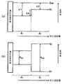
도 1 에 반도체 전자 구조의 파라미터를 나타낸다. 전자 친화력 (χ) 이란, 전자를 하나 부여하는 데에 필요로 하는 에너지를 의미하고, 반도체의 경우에는 전도체 하단 (Ec) 으로부터 진공 준위 (EVac) 까지의 에너지차를 가리킨다. 전자 친화력은 도 1 에 나타내는 바와 같이, 이온화 포텐셜 (I) 과 밴드 갭 에너지 (Eg) 의 차로부터 구하는 것이 가능하다. 이온화 포텐셜 (I) 은 광 전자 분광 측정으로부터, 밴드 갭 에너지 (Eg) 는 투과 스펙트럼 측정 및 반사 스펙트럼 측정으로부터 얻는 것이 가능하다.Figure 1 shows the parameters of the semiconductor electronic structure. The electron affinity (?) Means the energy required to impart one electron, and in the case of a semiconductor, the energy difference from the lower end (Ec) of the conductor to the vacuum level (EVac). As shown in Fig. 1, the electron affinity can be obtained from the difference between the ionization potential I and the band gap energy Eg. The ionization potential (I) can be obtained from photoelectron spectroscopy, and the band gap energy (Eg) can be obtained from transmission spectrum measurement and reflection spectrum measurement.
즉, 본 발명의 박막 트랜지스터는, 도 2a 에 그 포텐셜 구조를 나타내는 바와 같이, a (In2O3)·b (Ga2O3)·c (ZnO) 로 이루어지는 산화물 반도체층이 그 게이트 전극측 (도 2a 에 있어서는 게이트 절연막측) 으로부터 막 두께 방향으로 제 1 영역 (A1), 제 2 영역 (A2) 을 포함하고, 제 1 영역 (A1) 의 전자 친화력 (χ1) 이, 제 2 영역의 전자 친화력 (χ2) 보다 크게 우물형 포텐셜을 구성하고, 상기 제 2 영역의 b/(a + b) 를, 상기 제 1 영역의 b/(a + b) 보다 크게 함으로써, 제 1 영역 (A1) 과 제 2 영역 (A2) 의 전자 친화력차를 부여하는 것을 특징으로 한다.That is, in the thin film transistor of the present invention, as shown in the potential structure in Fig. 2A, an oxide semiconductor layer made of a (In2 O3 ) · b (Ga2 O3 ) · c (ZnO) the electron affinity (χ1) in the film thickness direction from a (gate insulating film side in Fig. 2a) the first region (a1), the second region, and including (a2) the first region (a1), the configuration of the well-type potential larger than the electron affinity (χ2) of the second region, and the second region b / (a + b) for, by greater than b / (a + b) of the first region, the first And the electron affinity difference between the region (A1 ) and the second region (A2 ) is given.
또한 여기서, 「영역」이란, 막 두께 방향에 있어서의 3 차원적인 영역 (부분) 을 나타내는 것이다. 또한, 산화물 반도체층의 제 1, 제 2 영역은 동종의 재료에 의해 구성되어 있는 것으로 하고 있다. 동종이란, 막을 구성하는 원소종이 동일하고, 카티온 조성비나 산소 농도가 상이한 것, 또는, 구성 원소의 일부에, 상이한 원소가 도프되어 있는 것을 의미한다. 예를 들어, 서로 Ga/(In + Ga) 가 상이한 IGZO 막은 동종이며, IGZO 막과 Zn 의 일부에 Mg 를 도프한 IGZO 막과는 동종이다.Here, the " region " refers to a three-dimensional region (portion) in the film thickness direction. It is also assumed that the first and second regions of the oxide semiconductor layer are made of the same kind of material. The same species means that the elemental paper constituting the film is the same, the cation composition ratio or the oxygen concentration is different, or a part of the constituent elements is doped with a different element. For example, the IGZO film of which Ga / (In + Ga) differs from each other is the same, and is similar to the IGZO film and the Mg-doped IGZO film in a part of Zn.
영역 (A1, A2) 에 있어서 b/(a + b) 를 변조함으로써 각 영역간에 포텐셜차 (전자 친화력차) 를 부여시킬 수 있다. 또, 영역 (A1) 의 산소 농도를 영역 (A2) 의 산소 농도보다 크게 함으로써, 추가적인 전자 친화력차를 부여할 수 있다. 본 발명에 있어서는 b/(a + b) 와 산소 농도를 동시에 변조시켜도 된다.A potential difference (electron affinity difference) can be given between the regions by modulating b / (a + b) in the regions A1 and A2 . Further, by increasing the oxygen concentration in the region A1 to be higher than the oxygen concentration in the region A2 , an additional electron affinity difference can be given. In the present invention, b / (a + b) and oxygen concentration may be simultaneously modulated.
여기서, 상기 제 1, 제 2 영역에 있어서의 카티온 조성비를 변조, 및/또는, 산소 농도 변조에 의한 전자 친화력차는 0.17 eV 이상, 1.3 eV 이하인 것이 바람직하고, 나아가서는, 제 1, 제 2 영역에 있어서의 전자 친화력차가 0.32 eV 이상, 1.3 eV 이하인 것이 바람직하다.Here, it is preferable that the electron affinity difference due to the modulation of the cation composition ratio and / or the oxygen concentration modulation in the first and second regions is 0.17 eV or more and 1.3 eV or less, and more preferably, It is preferable that the difference in electron affinity between them is 0.32 eV or more and 1.3 eV or less.
제 1, 제 2 영역의 전자 친화력차가, 0.17 eV 이상이면, 제 2 영역으로부터 제 1 영역으로 효율적으로 캐리어가 흘러들어, 높은 캐리어 농도와 이동도를 얻을 수 있다.When the difference in electron affinity between the first and second regions is 0.17 eV or more, the carrier flows efficiently from the second region to the first region, and high carrier concentration and mobility can be obtained.
또, 본 발명의 박막 트랜지스터에 있어서, 전자 친화력차를 증대시켜 가면 제 1 영역에 공급되는 캐리어량이 상승하여, 이동도가 증대되어 나가는 현상이 관찰된다. 산화물 반도체층 중의 In, Ga, Zn 중 Zn 조성비를 고정한 채로 b/(a + b) 를 변조하여 전자 친화력차를 증대시켜 가면 최대로 대략 1.3 eV 의 전자 친화력차가 얻어진다. 이 이상의 전자 친화력차를 얻기 위해서는 예를 들어, 활성층 중의 Zn 량을 대폭 변조하는 수법이 있지만, Zn 량을 대폭 변조하면 산화물 반도체층에 있어서의 아모르퍼스 구조가 불안정해져, TFT 특성의 불안정성, 불균일성을 초래하는 점에서, 상기 전자 친화력차는 1.3 eV 이하인 것이 바람직하다.Further, in the thin film transistor of the present invention, when the electron affinity difference is increased, the amount of carrier supplied to the first region increases, and the phenomenon that the mobility increases is observed. When the ratio b / (a + b) of In, Ga, and Zn in the oxide semiconductor layer is fixed and the electron affinity difference is increased, an electron affinity difference of about 1.3 eV is obtained at the maximum. In order to obtain an electron affinity greater than or equal to this, for example, there is a method of largely modifying the amount of Zn in the active layer. However, if the Zn amount is largely modulated, the amorphous structure in the oxide semiconductor layer becomes unstable and instability and nonuniformity It is preferable that the electron affinity difference is 1.3 eV or less.
본 발명의 박막 트랜지스터에 있어서는, 산화물 반도체층은 비정질막인 것이 바람직하다.In the thin film transistor of the present invention, the oxide semiconductor layer is preferably an amorphous film.
상기 산화물 반도체층이 비정질인지 여부는, X 선 회절 측정에 의해 확인할 수 있다. 즉, X 선 회절 측정에 의해, 결정 구조를 나타내는 명확한 피크가 검출되지 않은 경우에는, 그 산화물 반도체층은 비정질인 것으로 판단할 수 있다.Whether or not the oxide semiconductor layer is amorphous can be confirmed by X-ray diffraction measurement. That is, when no clear peak indicating a crystal structure is detected by X-ray diffraction measurement, it can be judged that the oxide semiconductor layer is amorphous.
본 발명의 박막 트랜지스터는, a (In2O3)·b (Ga2O3)·c (ZnO) 로 이루어지는 산화물 반도체를 활성층에 이용하여, 제 1 영역 (A1) 의 b/(a + b)) 가 0.5 보다 작은 것이 바람직하다.The transistor of the presentinvention, a (In 2 O 3) · b (Ga 2 O 3) · c using an oxide semiconductor made of a (ZnO) on the active layer, the first region (A1) of b / (a + b)) is less than 0.5.
더욱 바람직하게는, 제 1 영역 (A1) 의 b/(a + b) 가 0.4 보다 작고, 또한, 제 2 영역 (A2) 의 b/(a + b) 가 0.6 이상인 것이 바람직하다.More preferably not less than, the first region(A 1) b / (a + b) is less than 0.4, and the second area(A 2) b / (a + b) is 0.6 is preferred.
본 발명의 박막 트랜지스터에 있어서는, 상기 기판이 가요성을 갖는 것이 바람직하다.In the thin film transistor of the present invention, it is preferable that the substrate has flexibility.
가요성을 갖는 기판으로서는, 포화 폴리에스테르/폴리에틸렌테레프탈레이트 (PET) 계 수지 기판, 폴리에틸렌나프탈레이트 (PEN) 수지 기판, 가교 푸마르산디에스테르계 수지 기판, 폴리카보네이트 (PC) 계 수지 기판, 폴리에테르술폰 (PES) 수지 기판, 폴리술폰 (PSF, PSU) 수지 기판, 폴리아릴레이트 (PAR) 수지 기판, 고리형 폴리올레핀 (COP, COC) 수지 기판, 셀룰로오스계 수지 기판, 폴리이미드 (PI) 수지 기판, 폴리아미드이미드 (PAI) 수지 기판, 말레이미드-올레핀 수지 기판, 폴리아미드 (PA) 수지 기판, 아크릴계 수지 기판, 불소계 수지 기판, 에폭시계 수지 기판, 실리콘계 수지 필름 기판, 폴리벤즈아졸계 수지 기판, 에피술피드 화합물에 의한 기판, 액정 폴리머 (LCP) 기판, 시아네이트계 수지 기판, 방향족 에테르계 수지 기판, 산화규소 입자와의 복합 플라스틱 재료로 이루어지는 기판, 금속 나노 입자, 무기 산화물 나노 입자, 무기 질화물 나노 입자 등의 나노 입자와의 복합 플라스틱 재료로 이루어지는 기판, 금속계·무기계의 나노 화이버 및 마이크로 화이버와의 복합 플라스틱 재료로 이루어지는 기판, 카본 섬유, 카본나노튜브와의 복합 플라스틱 재료로 이루어지는 기판, 유리 페레이크, 유리 화이버, 유리 비즈와의 복합 플라스틱 재료로 이루어지는 기판, 점토 광물이나, 운모 파생 결정 구조를 갖는 입자와의 복합 플라스틱 재료로 이루어지는 기판, 얇은 유리와 상기 단독 유기 재료 사이에 적어도 1 회의 접합 계면을 갖는 적층 플라스틱 재료로 이루어지는 기판, 무기층 (예를 들어, SiO2, Al2O3, SiOxNy) 과 유기층을 교대로 적층함으로써, 적어도 1 회 이상의 접합 계면을 갖는 배리어 성능을 갖는 복합 재료로 이루어지는 기판, 스테인리스 기판, 스테인리스와 이종 금속을 적층한 금속 다층 기판, 알루미늄 기판, 표면에 산화 처리 (예를 들어, 양극 산화 처리) 를 실시함으로써, 표면의 절연성을 향상시킨 산화 피막 형성의 알루미늄 기판 등을 들 수 있다.Examples of the substrate having flexibility include a substrate made of a saturated polyester / polyethylene terephthalate (PET) resin substrate, a polyethylene naphthalate (PEN) resin substrate, a crosslinked fumaric acid diester resin substrate, a polycarbonate (PC) (PES) resin substrate, a polysulfone (PSF, PSU) resin substrate, a polyarylate (PAR) resin substrate, a cyclic polyolefin (COP, COC) resin substrate, a cellulosic resin substrate, (PAI) resin substrate, a maleimide-olefin resin substrate, a polyamide (PA) resin substrate, an acrylic resin substrate, a fluororesin substrate, an epoxy resin substrate, a silicone resin film substrate, a polybenzazole resin substrate, A liquid crystal polymer (LCP) substrate, a cyanate resin substrate, an aromatic ether resin substrate, a composite plastic with silicon oxide particles A substrate made of a composite plastic material with nanoparticles such as a metal nanoparticle, an inorganic oxide nanoparticle, and an inorganic nitride nanoparticle, a substrate made of a composite plastic material with metal and inorganic nanofibers and microfibers, a carbon fiber , A substrate made of a composite plastic material with carbon nanotubes, a substrate made of a composite plastic material with glass ferrite, a glass fiber, glass beads, a clay mineral, or a composite plastic material with particles having a mica- , thin glass and the sole substrate, the arms consisting of a multilayer plastic material having at least one time of the bonding interface between the organic material layer (e.g., SiO2, Al2 O3, SiOx Ny) and alternately stacked and the organic layer A composite structure having a barrier performance having at least one bonding interface (For example, an anodic oxidation treatment) is applied to a surface of a metal substrate, a stainless steel substrate, a metal multilayer substrate formed by laminating stainless and dissimilar metals, and an aluminum substrate. And the like.
본 발명의 제 1 박막 트랜지스터의 제조 방법은, 기판 상에, 활성층과, 소스 전극과, 드레인 전극과, 게이트 절연막과, 게이트 전극을 갖는 박막 트랜지스터로서, 상기 활성층이, 상기 게이트 전극측에 상기 게이트 절연막을 개재하여 배치된, 제 1 전자 친화력을 갖는 제 1 영역과, 상기 게이트 전극에 먼 측에 배치된, 상기 제 1 전자 친화력보다 작은 제 2 전자 친화력을 갖는 제 2 영역을 포함하고, 그 활성층의 막 두께 방향에 있어서, 상기 제 1 영역을 우물층, 상기 제 2 영역과 상기 게이트 절연막을 장벽층으로 하는 우물형 포텐셜이 구성되도록, 상기 활성층으로서, a (In2O3)·b (Ga2O3)·c (ZnO) 로 이루어지는 산화물 반도체층 (여기서 a, b, c 는, 각각 a ≥ 0, b ≥ 0, c ≥ 0, 또한 a + b ≠ 0, b + c ≠ 0, c + a ≠ 0 이다.) 을 스퍼터법에 의해 성막하는 성막 공정을 포함하고,A method of manufacturing a first thin film transistor of the present invention is a thin film transistor having an active layer, a source electrode, a drain electrode, a gate insulating film, and a gate electrode on a substrate, A first region having a first electron affinity and a second region having a second electron affinity smaller than the first electron affinity and disposed on a side farther from the gate electrode, A (In2 O3 ) · b (Ga (a)) is formed as the active layer so that the first region is a well layer, and the second region and the gate insulating film are a barrier layer in the film thickness direction of the2 O3) · c (the oxide semiconductor layer made of ZnO) (where a, b, c are, respectively, a ≥ 0, b ≥ 0, c ≥ 0, also a + b ≠ 0, b + c ≠ 0, c + a < / RTI > 0) is formed by the sputtering method And also,
그 성막 공정에 있어서, 성막실 내를 제 1 산소 분압/아르곤 분압 하에서 상기 제 1 영역을 성막하고, 상기 성막실 내를 제 2 산소 분압/아르곤 분압 하에서, 제 1 영역의 b/(a + b) 보다 큰 b/(a + b) 가 되는 조성비의 상기 제 2 영역을 성막하는 것을 특징으로 한다.In the film formation step, the first region is formed in the deposition chamber under a first partial pressure of oxygen gas / partial pressure of argon gas, and the second region b / (a + b (A + b) larger than the film thickness of the second region.
여기서, 상기 제 2 산소 분압/아르곤 분압을, 상기 제 1 산소 분압/아르곤 분압보다 작게 하는 것이 바람직하다.Here, it is preferable that the second oxygen partial pressure / argon partial pressure is made smaller than the first partial oxygen partial pressure / argon partial pressure.
본 발명의 제 2 박막 트랜지스터의 제조 방법은, 기판 상에, 활성층과, 소스 전극과, 드레인 전극과, 게이트 절연막과, 게이트 전극을 갖는 박막 트랜지스터로서, 상기 활성층이, 상기 게이트 전극측에 상기 게이트 절연막을 개재하여 배치된, 제 1 전자 친화력을 갖는 제 1 영역과, 상기 게이트 전극에 먼 측에 배치된, 상기 제 1 전자 친화력보다 작은 제 2 전자 친화력을 갖는 제 2 영역을 포함하고, 그 활성층의 막 두께 방향에 있어서, 상기 제 1 영역을 우물층, 상기 제 2 영역과 상기 게이트 절연막을 장벽층으로 하는 우물형 포텐셜이 구성되도록, 상기 활성층으로서, a (In2O3)·b (Ga2O3)·c (ZnO) 로 이루어지는 산화물 반도체층 (여기서 a, b, c 는, 각각 a ≥ 0, b ≥ 0, c ≥ 0, 또한 a + b ≠ 0, b + c ≠ 0, c + a ≠ 0 이다.) 을 스퍼터법에 의해 성막하는 성막 공정을 포함하고,A method of manufacturing a second thin film transistor of the present invention is a thin film transistor having an active layer, a source electrode, a drain electrode, a gate insulating film, and a gate electrode on a substrate, A first region having a first electron affinity and a second region having a second electron affinity smaller than the first electron affinity and disposed on a side farther from the gate electrode, A (In2 O3 ) · b (Ga (a)) is formed as the active layer so that the first region is a well layer, and the second region and the gate insulating film are a barrier layer in the film thickness direction of the2 O3) · c (the oxide semiconductor layer made of ZnO) (where a, b, c are, respectively, a ≥ 0, b ≥ 0, c ≥ 0, also a + b ≠ 0, b + c ≠ 0, c + a < / RTI > 0) is formed by the sputtering method And also,
그 성막 공정이, 상기 제 1 영역과, 제 1 영역의 b/(a + b) 보다 큰 b/(a + b) 가 되는 조성비의 상기 제 2 영역을 성막하는 공정을 포함하고, 상기 제 1 영역의 성막 중 및/또는 그 제 1 영역을 성막한 후에, 그 제 1 영역의 성막면에 산소 함유 라디칼을 조사하는 공정을 포함하는 것을 특징으로 한다.The film forming step includes a step of forming the first region and the second region having a composition ratio of b / (a + b) larger than b / (a + b) of the first region, And irradiating an oxygen-containing radical to the film-forming surface of the first region during film formation of the region and / or after film formation of the first region.
본 발명의 제 3 박막 트랜지스터의 제조 방법은, 기판 상에, 활성층과, 소스 전극과, 드레인 전극과, 게이트 절연막과, 게이트 전극을 갖는 박막 트랜지스터로서, 상기 활성층이, 상기 게이트 전극측에 상기 게이트 절연막을 개재하여 배치된, 제 1 전자 친화력을 갖는 제 1 영역과, 상기 게이트 전극에 먼 측에 배치된, 상기 제 1 전자 친화력보다 작은 제 2 전자 친화력을 갖는 제 2 영역을 포함하고, 그 활성층의 막 두께 방향에 있어서, 상기 제 1 영역을 우물층, 상기 제 2 영역과 상기 게이트 절연막을 장벽층으로 하는 우물형 포텐셜이 구성되도록, 상기 활성층으로서, a (In2O3)·b (Ga2O3)·c (ZnO) 로 이루어지는 산화물 반도체층 (여기서 a, b, c 는, 각각 a ≥ 0, b ≥ 0, c ≥ 0, 또한 a + b ≠ 0, b + c ≠ 0, c + a ≠ 0 이다.) 을 스퍼터법에 의해 성막하는 성막 공정을 포함하고,A method of manufacturing a third thin film transistor of the present invention is a thin film transistor having an active layer, a source electrode, a drain electrode, a gate insulating film, and a gate electrode on a substrate, A first region having a first electron affinity and a second region having a second electron affinity smaller than the first electron affinity and disposed on a side farther from the gate electrode, A (In2 O3 ) · b (Ga (a)) is formed as the active layer so that the first region is a well layer, and the second region and the gate insulating film are a barrier layer in the film thickness direction of the2 O3) · c (the oxide semiconductor layer made of ZnO) (where a, b, c are, respectively, a ≥ 0, b ≥ 0, c ≥ 0, also a + b ≠ 0, b + c ≠ 0, c + a < / RTI > 0) is formed by the sputtering method And also,
그 성막 공정이, 상기 제 1 영역과, 제 1 영역의 b/(a + b) 보다 큰 b/(a + b) 가 되는 조성비의 상기 제 2 영역을 성막하는 공정을 포함하고, 상기 제 1 영역의 성막 중 및/또는 제 1 영역의 성막 후에, 오존 분위기 중에서 그 제 1 영역의 성막면에 자외선을 조사하는 공정을 포함하는 것을 특징으로 한다.The film forming step includes a step of forming the first region and the second region having a composition ratio of b / (a + b) larger than b / (a + b) of the first region, And irradiating ultraviolet rays onto the film formation surface of the first region in an ozone atmosphere during film formation of the region and / or after film formation of the first region.
또한, 본 발명의 제 1 내지 제 3 박막 트랜지스터의 제조 방법에 있어서는, 모두 상기 성막 공정 동안, 성막 기판을 대기에 노출시키지 않는 것이 바람직하다.Further, in the first to third thin film transistor manufacturing methods of the present invention, it is preferable that all of the film formation substrates are not exposed to the atmosphere during the film formation process.
본 발명의 표시 장치는, 본 발명의 박막 트랜지스터를 구비한 것을 특징으로 하는 것이다.The display device of the present invention is characterized by including the thin film transistor of the present invention.
본 발명 이미지 센서는, 본 발명의 박막 트랜지스터를 구비한 것을 특징으로 하는 것이다.The image sensor of the present invention is characterized by including the thin film transistor of the present invention.
본 발명의 X 선 센서는, 본 발명의 박막 트랜지스터를 구비한 것을 특징으로 하는 것이다.The X-ray sensor of the present invention is characterized by including the thin film transistor of the present invention.
본 발명의 X 선 디지털 촬영 장치는, 본 발명의 X 선 센서를 구비한 것을 특징으로 하는 것이다.The X-ray digital photographing apparatus of the present invention is characterized by including the X-ray sensor of the present invention.
본 발명의 박막 트랜지스터는, a (In2O3)·b (Ga2O3)·c (ZnO) 로 이루어지는 산화물 반도체층의 제 1 영역이, 보다 전자 친화력이 작은 제 2 영역과 접하고 있고, 제 1 영역의 전도대 하단이 제 2 영역, 및 게이트 절연막을 포텐셜 장벽으로 하는 우물형 포텐셜 구조를 형성한다. 그 결과, 제 1 영역에 대한 전자 캐리어의 유입이 일어나, 제 1 영역의 조성비나 산소 결손량을 변화시키지 않고, 캐리어 밀도를 높일 수 있으므로 높은 이동도를 갖는 것으로 할 수 있다.In the thin film transistor of the present invention, the first region of the oxide semiconductor layer made of a (In2 O3 ) · b (Ga2 O3 ) · c (ZnO) is in contact with the second region having a smaller electron affinity, The lower region of the conduction band of the first region serves as the second region, and the gate insulating film serves as the potential barrier. As a result, the electron carrier is introduced into the first region, and the carrier density can be increased without changing the composition ratio or oxygen deficiency amount of the first region, so that it can have a high mobility.
일반적으로, 산화물 반도체에 있어서는, 캐리어 밀도를 높이기 위해서, 산소 결손량을 늘리는 것이 이루어지는데, 과잉인 산소 결손은 동시에 캐리어에 대한 산란체가 되어, 이동도를 저하시키는 요인이 된다. 본 발명에 있어서는, 우물층이 되는 제 1 영역에 있어서 산소 결손량을 늘릴 필요가 없기 때문에, 우물형 포텐셜 구조에 의한 캐리어의 증대에 더하여 채널층이 되는 제 1 영역 중의 산소 결손에 의한 이동도 저하가 억제되어, 추가적인 이동도의 향상이 가능하다.Generally, in an oxide semiconductor, in order to increase the carrier density, the amount of oxygen deficiency is increased. However, excessive oxygen deficiency becomes a scattering body for the carrier at the same time, which causes a decrease in mobility. In the present invention, since it is not necessary to increase the amount of oxygen deficiency in the first region that becomes the well layer, the mobility due to the oxygen deficiency in the first region that becomes the channel layer is lowered And further improvement of the mobility is possible.
본 발명의 박막 트랜지스터는 a (In2O3)·b (Ga2O3)·c (ZnO) 로 이루어지는 산화물 반도체층은, 제 1, 제 2 영역에 있어서 동종의 재료로 형성되어 있기 때문에, 채널층이 되는 제 1 영역이, 이종 재료와 접하고 있는 경우에 비해 계면에서의 결함 밀도가 저감되어, 균일성, 안정성, 신뢰성의 관점에서도 우수한 박막 트랜지스터를 제공할 수 있다. 또 동시에, 채널층이 되는 제 1 영역이 외기에 노출되어 있지 않기 때문에, 시간 경과적이나 소자가 놓여져 있는 환경 하에 의존하는 소자 특성 열화가 저감된다.In the thin film transistor of the present invention, since the oxide semiconductor layer made of a (In2 O3 ) · b (Ga2 O3 ) · c (ZnO) is formed of the same material in the first and second regions, The defect density at the interface is reduced as compared with the case where the first region which is a channel layer is in contact with the dissimilar material, and a thin film transistor excellent in uniformity, stability and reliability can be provided. At the same time, since the first region serving as a channel layer is not exposed to the outside air, the deterioration of device characteristics depending on an environment in which the device is placed over time is reduced.
본 발명에 있어서, 산화물 반도체층이 비정질막이면, 300 ℃ 이하의 저온에서 성막 가능하기 때문에, 플라스틱 기판과 같은 가요성이 있는 수지 기판에 형성하기 쉽다. 따라서 박막 트랜지스터 부착 플라스틱 기판을 사용한 플렉시블 디스플레이에 대한 적용이 보다 용이해진다. 게다가 비정질막은 대면적에 걸쳐서 균일한 막을 형성하기 쉽고, 다결정과 같은 입계가 존재하지 않기 때문에 소자 특성의 편차를 억제하는 것이 용이하다.In the present invention, if the oxide semiconductor layer is an amorphous film, the film can be formed at a low temperature of 300 캜 or less, and therefore, it is easy to form on a flexible resin substrate such as a plastic substrate. This makes it easier to apply to a flexible display using a plastic substrate with a thin film transistor. In addition, since the amorphous film is easy to form a uniform film over a large area, and there is no such a grain boundary as polycrystals, it is easy to suppress variations in device characteristics.
본 발명의 표시 장치는, 높은 이동도를 갖는 본 발명의 박막 트랜지스터를 구비하고 있으므로, 저소비 전력 또한 고품위인 표시를 실현할 수 있다.Since the display device of the present invention includes the thin film transistor of the present invention having high mobility, it is possible to realize display with low power consumption and high quality.
본 발명의 X 선 센서는, 신뢰성이 우수한 본 발명의 박막 트랜지스터를 구비하기 때문에, S/N 이 높아, 높은 감도 특성을 실현할 수 있다.Since the X-ray sensor of the present invention includes the thin film transistor of the present invention having high reliability, the S / N ratio is high and high sensitivity characteristics can be realized.
본 발명의 X 선 디지털 촬영 장치는, 그 X 선 센서에 높은 이동도를 갖는 트랜지스터를 구비하고 있으므로, 경량이고 플렉시블성을 갖고, 또한 넓은 다이나믹레인지의 화상이 얻어져, 그 고속성으로부터 특히 동영상 촬영에 바람직하다.Since the X-ray digital imaging apparatus of the present invention is provided with the transistor having high mobility in the X-ray sensor, it is possible to obtain a lightweight, flexible, and wide dynamic range image, .
도 1 은, 반도체 전자 구조의 파라미터를 설명하기 위한 도면이다.
도 2a 는, 전자 친화력차에 의한 포텐셜 구조를 나타내는 도면 및 도 2b 는 밴드 갭 에너지 구조를 나타내는 도면이다.
도 3a 는 탑 게이트-탑 콘택트형, 도 3b 는 탑 게이트-보텀 컨택트형, 도 3c 는 보텀 게이트-탑 콘택트형, 도 3d 는 보텀 게이트-보텀 컨택트형의 박막 트랜지스터의 구성을 모식적으로 나타내는 단면도이다.
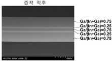
도 4 는 IGZO 적층막의 (A) 적층 직후, (B) 250 ℃ 어닐 처리 후, (C) 500 ℃ 어닐 처리 후를 나타내는 단면 STEM 이미지이다.
도 5 는 샘플 1 ∼ 5 에 대한 Tauc 플롯을 나타내는 도면이다.
도 6 은 도 5 로부터 안내된 밴드 갭 에너지의 조성비 의존을 나타내는 도면이다.
도 7 은 샘플 1 ∼ 5 에 대한 여기광 에너지와 규격화 광 전자 수율을 나타내는 도면이다.
도 8 은 도 7 로부터 구한 이온화 포텐셜의 조성 의존성을 나타내는 도면이다.
도 9 는 전자 친화력의 조성 의존성을 나타내는 도면이다.
도 10a 는 샘플 6, 7, 도 10b 는 샘플 8, 9 에 대한 Tauc 플롯을 나타내는 도면이다.
도 11 은 도 10 으로부터 안내된 밴드 갭 에너지의 산소 분압/아르곤 분압 의존성을 나타내는 도면이다.
도 12a 는 샘플 6, 7, 도 12b 는 샘플 8, 9 에 대한 여기광 에너지와 규격화 전자 수율을 나타내는 도면이다.
도 13 은 도 12 로부터 안내된 이온화 포텐셜의 산소 분압/아르곤 분압 의존성을 나타내는 도면이다.
도 14 는 전자 친화력의 산소 분압/아르곤 분압 의존성을 나타내는 도면이다.
도 15a 는 비저항, 도 15b 는 캐리어 밀도, 도 15c 는 이동도의 Ga/(In + Ga) 의존성을 각각 나타내는 도면이다.
도 16 은 실시형태의 액정 표시 장치의 일부분을 나타내는 개략 단면도이다.
도 17 은 도 16 의 액정 표시 장치의 전기 배선의 개략 구성도이다.
도 18 은 실시형태의 유기 EL 표시 장치의 일부분을 나타내는 개략 단면도이다.
도 19 는 도 18 의 유기 EL 표시 장치의 전기 배선의 개략 구성도이다.
도 20 은 실시형태의 X 선 센서 어레이의 일부분을 나타내는 개략 단면도이다.
도 21 은 도 20 의 X 선 센서 어레이의 전기 배선의 개략 구성도이다.
도 22 는 실시예 및 비교예의 Vg-Id 특성을 나타내는 도면이다.
도 23 은 실시예 1, 2, 3, 비교예 1 에 있어서의 이동도 μ 의 포텐셜 깊이 Δχ 의존성을 나타내는 도면이다.1 is a diagram for explaining parameters of a semiconductor electronic structure.
2A is a diagram showing a potential structure by an electron affinity difference, and FIG. 2B is a diagram showing a band gap energy structure.
FIG. 3A is a sectional view schematically showing the structure of a top gate-top contact type, FIG. 3B is a top gate-bottom contact type, FIG. 3C is a bottom gate-top contact type, to be.
4 is a cross-sectional STEM image of (I) immediately after the lamination of (A) the IGZO laminated film, (B) after annealing at 250 ° C, and (C) after annealing at 500 ° C.
5 is a diagram showing a Tauc plot for Samples 1-5.
6 is a graph showing the dependence of the band gap energy on the composition ratio as guided from FIG.
7 is a graph showing the excitation light energy and the normalized photoelectron yield for the
8 is a graph showing the composition dependence of the ionization potential obtained from Fig. 7. Fig.
Fig. 9 is a diagram showing composition dependence of electron affinity. Fig.
10A is a
Fig. 11 is a graph showing the oxygen partial pressure / argon partial pressure dependence of the band gap energy guided from Fig. 10; Fig.
12A is a
13 is a graph showing the oxygen partial pressure / argon partial pressure dependence of the ionization potential induced from FIG. 12. FIG.
14 is a graph showing the dependence of the electron affinity on the oxygen partial pressure / the argon partial pressure.
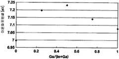
FIG. 15A is a diagram showing resistivity, FIG. 15B is a carrier density, and FIG. 15C is a diagram showing Ga / (In + Ga) dependence of mobility.
16 is a schematic cross-sectional view showing a part of the liquid crystal display device of the embodiment.
17 is a schematic configuration diagram of the electric wiring of the liquid crystal display device of Fig.
18 is a schematic cross-sectional view showing a part of the organic EL display device according to the embodiment.
19 is a schematic configuration diagram of the electric wiring of the organic EL display device of Fig.
20 is a schematic cross-sectional view showing a part of the X-ray sensor array of the embodiment.
21 is a schematic configuration diagram of the electric wiring of the X-ray sensor array of Fig.
22 is a graph showing Vg-Id characteristics of Examples and Comparative Examples.
23 is a graph showing the dependency of the mobility μ on the potential depth Δχ in Examples 1, 2 and 3 and Comparative Example 1. FIG.
이하, 본 발명의 실시형태에 대해 도면을 참조하여 설명한다.BEST MODE FOR CARRYING OUT THE INVENTION Hereinafter, embodiments of the present invention will be described with reference to the drawings.
<박막 트랜지스터><Thin Film Transistor>
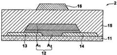
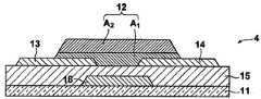
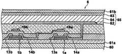
도 3a 내지 도 3d 는, 본 발명의 제 1 ∼ 제 4 실시형태의 박막 트랜지스터 (1 ∼ 4) 의 구성을 모식적으로 나타내는 단면도이다. 도 3a ∼ 도 3d 의 각 박막 트랜지스터에 있어서, 공통의 요소에는 동일한 부호를 부여하고 있다.Figs. 3A to 3D are cross-sectional views schematically showing the structures of the
본 발명의 실시형태에 관련된 박막 트랜지스터 (1 ∼ 4) 는, 기판 (11) 상에, 활성층 (12) 과, 소스 전극 (13) 과, 드레인 전극 (14) 과, 게이트 절연막 (15) 과, 게이트 전극 (16) 을 갖고, 활성층 (12) 이, 막 두께 방향으로 우물형 포텐셜을 구성하는 제 1, 제 2 영역 (A1, A2) 을 구비하고 있다 (도 3a ∼ 도 3d 참조).The
활성층 (12) 은 a (In2O3)·b (Ga2O3)·c (ZnO) 로 나타내는 산화물 반도체층 (IGZO 층) 으로 이루어지고, 제 1 영역 (A1) 은, 우물형 포텐셜 (도 2a 참조) 의 우물부가 되는 제 1 전자 친화력 (χ1) 을 갖는 영역이고, 제 2 영역 (A2) 은, 제 1 영역 (A1) 보다 게이트 전극 (16) 에 먼 측에 배치된, 제 1 전자 친화력 (χ1) 보다 작은 제 2 전자 친화력 (χ2) 을 갖고, 또한 제 1 영역보다 카티온 조성비 b/(a + b) 가 큰 것을 특징으로 하는 영역이다.The
또, 본 발명의 박막 트랜지스터 (1 ∼ 4) 에 있어서는, 제 1, 제 2 영역은 연속 성막되고, 제 1, 제 2 영역간에 전극층 등의 산화물 반도체층 이외의 층은 삽입되지 않는 것으로 한다.In the thin film transistors (1 to 4) of the present invention, it is assumed that the first and second regions are continuously formed, and a layer other than the oxide semiconductor layer such as an electrode layer is not inserted between the first and second regions.
영역 (A1, A2) 에 있어서 b/(a + b) 를 변조함으로써 각 영역간에 포텐셜차 (전자 친화력차) 를 부여시킬 수 있다. 또, 영역 (A1) 의 산소 농도를 영역 (A2) 의 산소 농도보다 크게 함으로써, 추가적인 전자 친화력차를 부여할 수 있어, 포텐셜 우물부에 효율적으로 캐리어를 집중시킬 수 있다. 동시에, 영역 (A1) 의 산소 농도를 높이는 것에 의해 불순물 산란에 의한 이동도의 저하를 억제하여, 추가적인 이동도의 향상이 가능하다. 본 발명에 있어서는 b/(a + b) 와 산소 농도를 동시에 변조시켜도 된다.A potential difference (electron affinity difference) can be given between the regions by modulating b / (a + b) in the regions A1 and A2 . Further, by making the oxygen concentration in the region A1 larger than the oxygen concentration in the region A2 , it is possible to impart a further difference in electron affinity and effectively concentrate the carriers in the potential well portion. At the same time, by increasing the oxygen concentration in the region A1 , it is possible to suppress the lowering of the mobility due to the impurity scattering and to further improve the mobility. In the present invention, b / (a + b) and oxygen concentration may be simultaneously modulated.
도 3a 에 나타내는 제 1 실시형태의 박막 트랜지스터 (1) 는, 탑 게이트-탑 콘택트형의 트랜지스터이고, 도 3b 에 나타내는 제 2 실시형태의 박막 트랜지스터 (2) 는, 탑 게이트-보텀 컨택트형의 트랜지스터이며, 도 3c 에 나타내는 제 3 실시형태의 박막 트랜지스터 (3) 는, 보텀 게이트-탑 콘택트형의 트랜지스터이고, 도 3d 에 나타내는 제 4 실시형태의 박막 트랜지스터 (4) 는, 보텀 게이트-보텀 컨택트형의 트랜지스터이다.The
도 3a ∼ 도 3d 에 나타내는 실시형태는, 게이트, 소스, 드레인 전극의, 활성층 (IGZO 층) 에 대한 배치가 상이한데, 동일 부호가 부여되어 있는 각 요소의 기능은 동일하고, 동일한 재료를 적응할 수 있다.In the embodiment shown in Figs. 3A to 3D, the arrangement of the gate, source, and drain electrodes in the active layer (IGZO layer) is different, but the functions of each element to which the same reference numerals are assigned are the same, have.
이하, 각 구성 요소에 대해 상세하게 서술한다.Hereinafter, each component will be described in detail.
(기판)(Board)
박막 트랜지스터 (1) 를 형성하기 위한 기판 (11) 형상, 구조, 크기 등에 대해서는 특별히 제한은 없고, 목적에 따라 적절하게 선택할 수 있다. 기판의 구조는 단층 구조여도 되고, 적층 구조여도 된다. 기판 (11) 으로서는, 예를 들어, YSZ (이트륨 안정화 지르코늄) 나 유리 등의 무기 재료, 수지나 수지 복합 재료 등으로 이루어지는 기판을 사용할 수 있다. 그 중에서도 경량인 점, 가요성을 갖는 점으로부터 수지 혹은 수지 복합 재료로 이루어지는 기판이 바람직하다. 구체적으로는, 폴리부틸렌테레프탈레이트, 폴리에틸렌테레프탈레이트, 폴리에틸렌나프탈레이트, 폴리부틸렌나프탈레이트, 폴리스티렌, 폴리카보네이트, 폴리술폰, 폴리에테르술폰, 폴리아릴레이트, 알릴디글리콜카보네이트, 폴리아미드, 폴리이미드, 폴리아미드이미드, 폴리에테르이미드, 폴리벤즈아졸, 폴리페닐렌설파이드, 폴리시클로올레핀, 노르보르넨 수지, 폴리클로로트리플루오로에틸렌 등의 불소 수지, 액정 폴리머, 아크릴 수지, 에폭시 수지, 실리콘 수지, 아이오노머 수지, 시아네이트 수지, 가교 푸마르산 디에스테르, 고리형 폴리올레핀, 방향족 에테르, 말레이미드-올레핀, 셀룰로오스, 에피술피드 화합물 등의 합성 수지로 이루어지는 기판, 이미 서술한 합성 수지 등과 산화규소 입자의 복합 플라스틱 재료로 이루어지는 기판, 이미 서술한 합성 수지 등과 금속 나노 입자, 무기 산화물 나노 입자 혹은 무기 질화물 나노 입자 등과의 복합 플라스틱 재료로 이루어지는 기판, 이미 서술한 합성 수지 등과 카본 섬유 혹은 카본 나노 튜브의 복합 플라스틱 재료로 이루어지는 기판, 이미 서술한 합성 수지 등과 유리 페레이크, 유리 화이버 혹은 유리 비즈와의 복합 플라스틱 재료로 이루어지는 기판, 이미 서술한 합성 수지 등과 점토 광물 혹은 운모 파생 결정 구조를 갖는 입자의 복합 플라스틱 재료로 이루어지는 기판, 얇은 유리와 이미 서술한 어느 것의 합성 수지 사이에 적어도 1 회의 접합 계면을 갖는 적층 플라스틱 기판, 무기층과 유기층 (이미 서술한 합성 수지) 을 교대로 적층함으로써, 적어도 1 회 이상의 접합 계면을 갖는 배리어 성능을 갖는 복합 재료로 이루어지는 기판, 스테인리스 기판 또는 스테인리스와 이종 금속을 적층한 금속 다층 기판, 알루미늄 기판 또는 표면에 산화 처리 (예를 들어 양극 산화 처리) 를 실시함으로써 표면의 절연성을 향상시킨 산화 피막 형성의 알루미늄 기판 등을 사용할 수 있다.The shape, structure, size, etc. of the
또한, 수지 기판으로서는, 내열성, 치수 안정성, 내용제성, 전기 절연성, 가공성, 저통기성, 및 저흡습성 등이 우수한 것이 바람직하다. 수지 기판은, 수분이나 산소의 투과를 방지하기 위한 가스 배리어층이나, 수지 기판의 평탄성이나 하부 전극과의 밀착성을 향상시키기 위한 언더코트층 등을 구비하고 있어도 된다.The resin substrate is preferably excellent in heat resistance, dimensional stability, solvent resistance, electrical insulation, workability, low air permeability, and low hygroscopicity. The resin substrate may be provided with a gas barrier layer for preventing permeation of water or oxygen, an undercoat layer for improving the flatness of the resin substrate and adhesion with the lower electrode, and the like.
또, 기판의 두께는 50 ㎛ 이상 500 ㎛ 이하인 것이 바람직하다. 기판의 두께가 50 ㎛ 이상이면, 기판 자체의 평탄성이 보다 향상된다. 기판의 두께가 500 ㎛ 이하이면, 기판 자체의 가요성이 보다 향상되어, 플렉시블 디바이스용 기판으로서의 사용이 보다 용이해진다. 또한, 기판을 구성하는 재료에 따라, 충분한 평탄성 및 가교성을 갖는 두께는 상이하기 때문에, 기판 재료에 따라 그 두께를 설정할 필요가 있지만, 대체로 그 범위는 50 ㎛ ∼ 500 ㎛ 의 범위가 된다.It is also preferable that the thickness of the substrate is 50 占 퐉 or more and 500 占 퐉 or less. When the thickness of the substrate is 50 mu m or more, the flatness of the substrate itself is further improved. When the thickness of the substrate is 500 m or less, the flexibility of the substrate itself is further improved, and the substrate is more easily used as a substrate for a flexible device. In addition, since the thickness of the substrate having sufficient flatness and crosslinkability differs depending on the material constituting the substrate, it is necessary to set the thickness thereof in accordance with the substrate material, but the range usually ranges from 50 m to 500 m.
(활성층)(Active layer)
활성층 (12) 은 IGZO 막, 보다 상세하게는 a (In2O3)·b (Ga2O3)·c (ZnO) 로 이루어지고, 제 1, 제 2 전자 친화력 (χ1, χ2) 을 각각 갖는 제 1, 제 2 영역 (A1, A2) 을 구비하고, 제 1 전자 친화력 (χ1) 이 제 2 전자 친화력 (χ2) 보다 크고, 또한 영역 (A2) 에 있어서의 b/a + b 가, 영역 (A1) 에 있어서의 b/(a + b) 보다 큰 것을 특징으로 한다.The
적층 방향으로 우물형 포텐셜을 형성시키기 위해서는, 각 영역간에서 b/(a + b) 를 변조함으로써 각 영역의 전자 친화력차를 부여시킨다. 또, 제 1 영역 (A1) 과 제 2 영역 (A2) 은 포텐셜의 차는 제 2 영역 (A2) 의 산소 농도를, 제 1 영역 (A1) 의 산소 농도보다 낮게 함으로써도 우물형 포텐셜을 형성하는 전자 친화력차를 부여할 수 있다. 각 영역이 공통의 원소 조성비에 의해 구성되어 이루어지는 경우, 산소 농도가 높을수록 전자 친화력이 크다.In order to form the well potential in the stacking direction, the electron affinity difference of each region is given by modulating b / (a + b) between the regions. In addition, the first region (A1) and a second area (A2) is the difference between the potential of the oxygen concentration of the second region (A2), the first region is also a well-type potential by less than the oxygen concentration of (A1) The electron affinity difference can be imparted. When each region is constituted by a common element composition ratio, the higher the oxygen concentration, the greater the electron affinity.
여기서, 상기 제 1, 제 2 영역에 있어서의 b/(a + b) 를 변조, 및 산소 농도 변조에 의한 전자 친화력차는 0.17 eV 이상, 1.3 eV 이하인 것이 바람직하고, 나아가서는, 제 1, 제 2 영역에 있어서의 전자 친화력차가 0.32 eV 이상, 1.3 eV 이하인 것이 바람직하다.Here, it is preferable that the electron affinity difference due to the modulation and the oxygen concentration modulation in the first and second regions is 0.17 eV or more and 1.3 eV or less, and more preferably, the first and second It is preferable that the electron affinity difference in the region is 0.32 eV or more and 1.3 eV or less.
제 1, 제 2 영역의 전자 친화력차가, 0.17 eV 이상이면, 제 2 영역으로부터 제 1 영역에 효율적으로 캐리어가 흘러들어, 높은 캐리어 농도와 고이동도를 얻을 수 있다.When the difference in electron affinity between the first and second regions is 0.17 eV or more, the carrier flows efficiently from the second region to the first region, and high carrier concentration and high mobility can be obtained.
또, 본 발명의 박막 트랜지스터에 있어서, 전자 친화력차를 증대시켜 가면 제 1 영역에 공급되는 캐리어량이 상승하여, 이동도가 증대되어 나가는 현상이 관찰된다. 산화물 반도체층 중의 In, Ga, Zn 중 Zn 조성비를 고정시킨 채로 b/(a + b) 를 변조하여 전자 친화력차를 증대해 나가면 최대로 대략 1.3 eV 의 전자 친화력차가 얻어진다. 이 이상의 전자 친화력차를 얻기 위해서는 예를 들어, 활성층 중의 Zn 량을 대폭 변조하는 수법이 있는데, Zn 량을 대폭 변조하면 산화물 반도체층에 있어서의 아모르퍼스 구조가 불안정해져, TFT 특성의 불안정성, 불균일성을 초래하기 때문에, 상기 전자 친화력차는 1.3 eV 이하인 것이 바람직하다.Further, in the thin film transistor of the present invention, when the electron affinity difference is increased, the amount of carrier supplied to the first region increases, and the phenomenon that the mobility increases is observed. When the difference in electron affinity is increased by modulating b / (a + b) while keeping the Zn composition ratio among In, Ga and Zn in the oxide semiconductor layer fixed, an electron affinity difference of about 1.3 eV is obtained at the maximum. In order to obtain an electron affinity greater than or equal to this, for example, there is a method of largely modifying the amount of Zn in the active layer. If the amount of Zn is largely modulated, the amorphous structure in the oxide semiconductor layer becomes unstable and instability and nonuniformity , The electron affinity difference is preferably 1.3 eV or less.
산소 농도의 제어는, 구체적으로는 제 2 영역의 성막시에는 상대적으로 산소 분압이 낮은 조건으로 성막을 하고, 제 1 영역에 대해서는 성막시의 상대적으로 산소 분압이 높은 조건으로 성막을 함으로써, 혹은, 제 1 영역 성막 후에 산소 라디칼이나 오존을 조사하는 처리를 실시하는 것에 의해 막의 산화를 촉진시켜, 제 1 영역 중의 산소 결손량을 저감시키거나 하여 실시할 수 있다.Specifically, the oxygen concentration can be controlled by performing the film formation under the condition that the oxygen partial pressure is relatively low during the film formation of the second region and the film formation under the condition where the oxygen partial pressure is relatively high during the film formation in the first region, The oxygen radical and ozone are irradiated after the film formation of the first region to accelerate the oxidation of the film so as to reduce the oxygen deficiency amount in the first region.
또한, 제 1 영역의 산소 결손량은 극히 적게 하는 것이 바람직하다. 종래 산화물 반도체층을 채널층으로서 사용하는 경우에는, 이동도를 높이기 위해서 캐리어 밀도를 어느 정도 늘릴 필요가 있어, 산소 결손을 의도적으로 형성하는, 즉 산소 농도를 낮게 하는 것이 이루어졌다. 그러나 산소 결손이 많으면 산소 결함 자체가 캐리어에 대한 산란체가 되어 이동도의 저하를 초래한다는 문제가 있었다. 본 발명에서는 채널층으로서의 캐리어는, 제 2 영역으로부터 공급되기 때문에, 제 1 영역의 산소 결손량을 극히 적은 상태로 해도 충분한 캐리어 밀도, 거기에 따르는 이동도가 얻어진다.It is also preferable that the oxygen deficiency amount in the first region is extremely small. Conventionally, when the oxide semiconductor layer is used as a channel layer, it is necessary to increase the carrier density to some extent in order to increase the mobility, thereby intentionally forming an oxygen defect, that is, lowering the oxygen concentration. However, when oxygen deficiency is large, there is a problem that the oxygen defect itself becomes a scattering body for the carrier, resulting in a decrease in mobility. In the present invention, since the carrier serving as the channel layer is supplied from the second region, even if the oxygen deficiency amount in the first region is extremely small, a sufficient carrier density and mobility can be obtained.
본 발명의 박막 트랜지스터는 상기 산화물 반도체층의 제 1 영역 (A1) 의 b/(a + b) 를, 제 2 영역 (A2) 의 b/(a + b) 보다 작은 것으로 하는 것이 바람직하다. 또한, 제 1 영역 (A1) 의 b/(a + b) 가 0.5 이하인 것이 바람직하다. 더욱 바람직하게는, 제 1 영역 (A1) 의 a/a + b 가 0.6 이상이고 또한, 제 2 영역 (A2) 의 b/a + b 가 0.6 이상인 것이 바람직하다.In the thin film transistor of the present invention, b / (a + b) of the first region A1 of the oxide semiconductor layer is preferably smaller than b / (a + b) of the second region A2 . It is also preferable that b / (a + b) of the first region A1 is 0.5 or less. More preferably, it is preferable that a / a + b of the first region A1 is 0.6 or more and b / a + b of the second region A2 is 0.6 or more.
제 1 영역과, 제 2 영역의 b/(a + b) 의 차를 크게 함으로써, 전도대 하단의 에너지차가 커져, 효율적으로 전자 캐리어를 제 1 영역에 국재시키는 것이 가능해진다.By increasing the difference between b / (a + b) in the first region and the second region, the energy difference at the lower end of the conduction band becomes large, and the electron carrier can be efficiently localized in the first region.
또한, 본 발명에 있어서의 활성층 구성하는 제 1 영역의 Zn/In + Ga (전술한 일반식에 있어서는 2c/(a + b) 에 상당) 는 0.5 이상인 것이 바람직하고, 제 2 영역의 2c/(a + b) 는 0.5 이하인 것이 바람직하다. 2c/(a + b) 가 커짐으로써 광학 흡수단이 장파장측에 시프트되고, 2/(a + b) 가 커짐으로써 밴드 갭이 좁아진다. 그 때문에 제 1 영역에 상대적으로 2c/(a + b) 가 큰 IGZO 층을 배치하고, 제 2 영역에 상대적으로 2c/(a + b) 가 작은 IGZO 층을 배치함으로써 전도대 하단의 에너지차를 얻을 수 있어, 전자 캐리어를 제 1 영역에 국재시키는 것이 가능하다. 2c/(a + b) 를 제어하는 수법은 b/(a + b) 의 차를 크게 한 막에 적용시킴으로써, 보다 깊은 우물형 포텐셜 구조를 형성하는 것이 가능하고, 당연히 b/(a + b) 가 각 영역에서 동일한 경우에 있어서도 사용하는 것이 가능하다.It is preferable that Zn / In + Ga (corresponding to 2c / (a + b) in the above-mentioned general formula) of the first region constituting the active layer in the present invention is 0.5 or more and 2c / a + b) is preferably 0.5 or less. 2c / (a + b) is increased, the optical absorption edge is shifted to the longer wavelength side, and 2 / (a + b) is increased, thereby narrowing the band gap. Therefore, an IGZO layer having a large 2c / (a + b) is arranged in the first region and an IGZO layer having a small 2c / (a + b) is arranged in the second region to obtain an energy difference at the bottom of the conduction band And it is possible to cause the electron carrier to be localized in the first area. (A + b), it is possible to form a deeper well potential structure by applying the difference between b / (a + b) It is possible to use the same in the same region.
또, IGZO 로 이루어지는 산화물 반도체층의 Zn의 일부를, 보다 밴드 갭이 넓어지는 원소 이온을 도프함으로써, 보다 깊은 우물형 포텐셜 구조를 얻을 수 있다. 구체적으로는, Mg 를 도프함으로써 막의 밴드 갭을 크게 하는 것이 가능하다. 예를 들어, 제 2 영역에만 Mg 를 도프함으로써, 보다 깊은 우물형 포텐셜 구조를 형성할 수 있다. 또, 제 1 영역과, 제 2 영역 사이에, b/(a + b) 및 2c/(a + b) 에 차를 갖게 한 상태에서, 각 영역에 Mg 를 도프함으로써, In, Ga, Zn 만의 조성비를 제어한 계에 비해, 우물 장벽의 높이를 유지한 채로, 전체의 밴드 갭을 넓게 할 수 있다.Further, by doping a part of Zn of the oxide semiconductor layer made of IGZO with element ions having a wider bandgap, a deeper well potential structure can be obtained. Specifically, it is possible to increase the bandgap of the film by doping Mg. For example, by doping Mg only in the second region, a deeper well potential structure can be formed. Further, by doping Mg in each region with a difference between b / (a + b) and 2c / (a + b) between the first region and the second region, The entire band gap can be widened while maintaining the height of the well barriers as compared with the system in which the composition ratio is controlled.
유기 EL 에 사용되는 청색 발광층은 λ = 450 ㎚ 정도로 피크를 갖는 브로드한 발광을 나타내기 때문에, 만일 IGZO 막의 광학 밴드 갭이 비교적 좁고, 그 영역에 광학 흡수를 갖는 경우에는, 트랜지스터의 임계값 시프트가 일어나 버린다는 문제가 생긴다. 따라서, 특히 유기 EL 구동용으로 사용되는 박막 트랜지스터로서는, 채널층에 사용하는 재료의 밴드 갭이, 보다 큰 것이 바람직하다.Since the blue light emitting layer used for the organic EL shows broad light emission having a peak at about? = 450 nm, if the optical band gap of the IGZO film is relatively narrow and optical absorption is present in the region, the threshold shift of the transistor is There is a problem of getting up. Therefore, in particular, as the thin film transistor used for driving the organic EL, it is preferable that the band gap of the material used for the channel layer is larger.
IGZO 에 있어서 b/(a + b) 를 크게 하면 광학 흡수단이 단파장측에 시프트되어, 밴드 갭이 넓어지는데, 그와 동시에 b/(a + b) 가 큰 조성으로 함으로써 전기 전도성이 저하된다. 즉, b/(a + b) 가 큰 IGZO 막을 단독으로 박막 트랜지스터에 사용한 경우에는, 구하는 트랜지스터 특성 (구체적으로는, 수 십 ∼ 100 ㎠/Vs 를 초과하는 이동도) 은 얻어지지 않는다 (도 15c 참조.). 본 발명에서는, 밴드 갭이 넓고 b/(a + b) 가 큰 IGZO 층 (제 2 영역) 과 상대적으로 벤드 갭이 좁고 b/(a + b) 가 작은 IGZO 층 (제 1 영역) 을 접합한 구조를 사용함으로써, 게이트 절연막과 활성층으로 이루어지는 우물형 포텐셜이 형성되어, 제 1 영역에 캐리어를 국재화시키는 것이 가능해진다.When the ratio of b / (a + b) is increased in IGZO, the optical absorption edge is shifted to the short wavelength side to widen the band gap. At the same time, the composition having a large b / (a + b) decreases the electrical conductivity. That is, when the IGZO film having a large b / (a + b) is used for the thin film transistor alone, transistor characteristics (specifically, mobility exceeding several tens to 100 cm2 / Vs) Reference.). In the present invention, an IGZO layer (second region) having a wide band gap and a large b / (a + b) and an IGZO layer (first region) having a narrow bend gap and a small b / Structure, a well potential is formed by the gate insulating film and the active layer, and the carrier can be localized in the first region.
제 1 영역의 캐리어 밀도는 제 2 산소 결손량 제어나 카티온 도프에 의해 임의로 제어할 수 있다. 캐리어 밀도를 늘리고자 할 때에는 제 2 영역의 산소 결손량을 늘리거나, 또는 상대적으로 가수가 큰 카티온이 되기 쉬운 재료 (예를 들어 Ti, Zr, Hf, Ta 등) 를 도프하면 된다. 단, 가수가 큰 카티온을 도프하는 경우에는, 산화물 반도체막의 구성 원소 수가 증가하기 때문에, 성막 프로세스의 단순화, 저비용화의 면에서 불리한 점에서, 산소 농도 (산소 결손량) 에 의해, 캐리어 밀도를 제어하는 것이 바람직하다.The carrier density of the first region can be arbitrarily controlled by the second oxygen deficiency amount control or the cation dope. When the carrier density is to be increased, the amount of oxygen deficiency in the second region may be increased, or a material (for example, Ti, Zr, Hf, Ta or the like) that is relatively prone to become cations may be doped. However, when doping a large cation with cations, the number of constituent elements of the oxide semiconductor film is increased, so that the carrier density is reduced by oxygen concentration (oxygen deficiency amount) in view of simplification of the film formation process and lowering of cost. .
또한, 300 ℃ 이하의 온도에서 성막이 가능하다는 점에서, 산화물 반도체층은 비정질인 것이 바람직하다. 예를 들어, 비정질 IGZO 막은 기판 온도 200 ℃ 이하에서 성막 가능하다.Further, the oxide semiconductor layer is preferably amorphous in that film formation is possible at a temperature of 300 ° C or lower. For example, an amorphous IGZO film can be formed at a substrate temperature of 200 ° C or lower.
활성층 (12) 의 토탈의 막 두께 (총 막 두께) 는 10 ∼ 200 ㎚ 정도인 것이 바람직하다.The total thickness (total film thickness) of the
(소스·드레인 전극)(Source and drain electrodes)
소스 전극 (13) 및 드레인 전극 (14) 은 모두 높은 도전성을 갖는 것이면 특별히 제한 없고, 예를 들어 Al, Mo, Cr, Ta, Ti, Au, Ag 등의 금속, Al-Nd, 산화주석, 산화아연, 산화인듐, 산화인듐주석 (ITO), 산화아연인듐 (IZO) 등의 금속 산화물 도전막 등을, 단층 또는 2 층 이상의 적층 구조로서 사용할 수 있다.The
소스 전극 (13) 및 드레인 전극 (14) 은 모두, 예를 들어 인쇄 방식, 코팅 방식 등의 습식 방식, 진공 증착법, 스퍼터링법, 이온 플레이팅법 등의 물리적 방식, CVD, 플라스마 CVD 법 등의 화학적 방식 등 중에서 사용하는 재료와의 적성을 고려하여 적절하게 선택한 방법에 따라 성막하면 된다.The
소스 전극 (13) 및 드레인 전극 (14) 을, 상기 금속에 의해 구성하는 경우, 성막성, 에칭이나 리프트 오프법에 의한 패터닝성 및 도전성 등을 고려하면, 그 두께는, 10 ㎚ 이상, 1000 ㎚ 이하로 하는 것이 바람직하고, 50 ㎚ 이상, 100 ㎚ 이하로 하는 것이 보다 바람직하다.When the
(게이트 절연막)(Gate insulating film)
게이트 절연막 (15) 으로서는, 높은 절연성을 갖는 것이 바람직하고, 예를 들어 SiO2, SiNx, SiON, Al2O3, Y2O3, Ta2O5, HfO2 등의 절연막, 또는 이들 화합물을 적어도 2 개 이상 함유하는 절연막 등으로 구성할 수 있다.As the
게이트 절연막 (15) 은, 인쇄 방식, 코팅 방식 등의 습식 방식, 진공 증착법, 스퍼터링법, 이온 플레이팅법 등의 물리적 방식, CVD, 플라스마 CVD 법 등의 화학적 방식 등 중에서 사용하는 재료와의 적성을 고려하여 적절하게 선택한 방법에 따라 성막하면 된다.The
또한, 게이트 절연막 (15) 은 리크 전류의 저하 및 전압 내성의 향상을 위해서 충분한 두께를 가질 필요가 있는 한편, 두께가 지나치게 크면 구동 전압의 상승을 초래한다. 게이트 절연막 (15) 의 두께는, 재질에 따라 다르기도 하지만, 10 ㎚ ∼ 10 ㎛ 가 바람직하고, 50 ㎚ ∼ 1000 ㎚ 가 보다 바람직하고, 100 ㎚ ∼ 400 ㎚ 가 특히 바람직하다.In addition, the
(게이트 전극)(Gate electrode)
게이트 전극 (16) 으로서는, 높은 도전성을 갖는 것이면 특별히 제한 없고, 예를 들어 Al, Mo, Cr, Ta, Ti, Au, Ag 등의 금속, Al-Nd, 산화주석, 산화아연, 산화인듐, 산화인듐주석 (ITO), 산화아연인듐 (IZO) 등의 금속 산화물 도전막 등을, 단층 또는 2 층 이상의 적층 구조로서 사용할 수 있다.As the
게이트 전극 (16) 은, 예를 들어 인쇄 방식, 코팅 방식 등의 습식 방식, 진공 증착법, 스퍼터링법, 이온 플레이팅법 등의 물리적 방식, CVD, 플라스마 CVD 법 등의 화학적 방식 등 중에서 사용하는 재료와의 적성을 고려하여 적절하게 선택한 방법에 따라 성막하면 된다.The
게이트 전극 (16) 을, 상기 금속에 의해 구성하는 경우, 성막성, 에칭이나 리프트 오프법에 의한 패터닝성 및 도전성 등을 고려하면, 그 두께는, 10 ㎚ 이상, 1000 ㎚ 이하로 하는 것이 바람직하고, 50 ㎚ 이상, 200 ㎚ 이하로 하는 것이 보다 바람직하다.When the
(박막 트랜지스터의 제조 방법)(Thin Film Transistor Manufacturing Method)
도 3a 에 나타내는 탑 게이트-탑 콘택트형의 박막 트랜지스터 (1) 의 제조 방법에 대해 간단하게 설명한다. 기판 (11) 을 준비하고, 기판 (11) 상에 활성층 (IGZO 막) (12) 을, 제 2 영역 (A2), 제 1 영역 (A1) 의 순서로 스퍼터법 등의 성막 수법에 의해 성막한다. 이어서 활성층 (12) 을 패터닝한다. 패터닝은 포토리소그래피 및 에칭에 의해 실시할 수 있다. 구체적으로는, 잔존시키는 부분에 포토리소그래피에 의해 레지스트 패턴을 형성하고, 염산, 질산, 묽은 황산, 또는 인산, 질산 및 아세트산의 혼합액 등의 산용액에 의해 에칭함으로써 패턴을 형성한다.A manufacturing method of the top gate-top contact type
다음으로, 활성층 (12) 위에 소스·드레인 전극 (13, 14) 을 형성하기 위한 금속막을 형성한다. 이어서 금속막을 에칭 또는 리프트 오프법에 의해 소정 형상으로 패터닝하고, 소스 전극 (13) 및 드레인 전극 (14) 을 형성한다. 이 때, 소스·드레인 전극 (13, 14) 및 도시되지 않은, 이들 전극에 접속하는 배선을 동시에 패터닝하는 것이 바람직하다.Next, a metal film for forming the source /
소스·드레인 전극 (13, 14) 및 배선을 형성한 후, 게이트 절연막 (15) 을 형성한다. 게이트 절연막 (15) 은 포토리소그래피 및 에칭에 의해 소정 형상으로 패터닝 형성된다.After the source /
게이트 절연막 (15) 을 형성한 후, 게이트 전극 (16) 을 형성한다. 전극막을 성막 후, 에칭 또는 리프트오프법에 의해 소정 형상으로 패터닝하여, 게이트 전극 (16) 을 형성한다. 이 때, 게이트 전극 (16) 게이트 배선을 동시에 패터닝하는 것이 바람직하다.After the
이상의 순서에 따라, 도 3A 에 나타내는 박막 트랜지스터 (1) 를 제작할 수 있다.According to the above procedure, the
(활성층의 성막 공정)(Step of forming the active layer)
다음으로, 활성층의 성막 공정에 대해, 보다 상세하게 설명한다. 활성층 (12) 의 토탈의 막 두께 (총 막 두께) 는 10 ∼ 200 ㎚ 정도가 바람직하고, 각 영역은 대기 중에 노출되지 않고 연속하여 성막되는 것이 바람직하다. 대기 중에 노출되지 않고 연속하여 성막됨으로써, 결과적으로, 보다 우수한 트랜지스터 특성을 얻을 수 있다. 또, 성막 공정 수를 삭감할 수 있기 때문에, 제조 비용도 저감할 수 있다.Next, the process of forming the active layer will be described in more detail. The total film thickness (total film thickness) of the
여기서, 도 3c, 도 3d 에 나타내는 바와 같은 보텀 게이트형의 박막 트랜지스터 제조시에 대하여 설명한다. 이미 서술한 바와 같이, 보텀 게이트형의 박막 트랜지스터의 제조시에는 제 1 영역 (A1), 제 2 영역 (A2) 의 순서로 성막한다. 또한, 탑 게이트형의 박막 트랜지스터의 제조시에는, 활성층은, 제 2 영역 (A2), 제 1 영역 (A1) 의 순서로 성막하게 된다.Here, a description will be given of the manufacture of the bottom gate type thin film transistor as shown in Figs. 3C and 3D. As described above, the first region A1 and the second region A2 are formed in this order at the time of manufacturing the bottom gate type thin film transistor. Further, at the time of manufacturing the top gate type thin film transistor, the active layer is formed in the order of the second region (A2 ) and the first region (A1 ).
먼저, 제 1 영역 (A1) 을 성막한다. 여기서, 예를 들어, 제 1 영역 (A1) 으로서, Ga/(In + Ga) = 0.25, Zn/(In + Ga) = 0.5 인 IGZO 막을 막 두께 10 ㎚ 가 되도록 형성한다.First, the first region A1 is formed. Here, for example, a form such that the first region (A1) As, Ga / (In + Ga) = 0.25, Zn / (In + Ga) = 10 ㎚ film thickness of the IGZO film is 0.5.
상기와 같은 금속 원소의 조성비가 되도록 성막하는 수법으로서, 스퍼터 성막이면 In, Ga, Zn, 또는 이들 산화물 혹은 이들 복합 산화물의 타겟을 조합하여 사용한 공스퍼터여도 되고, 미리, 성막한 IGZO 막 중의 금속 원소의 조성비가 상기가 되는 복합 산화물 타겟의 단독 스퍼터여도 된다. 성막 중의 기판 온도는 기판에 따라 임의로 선택해도 되는데, 플렉시블 기판을 사용하는 경우에는 기판 온도는 보다 실온에 가까운 것이 바람직하다.As a method of forming the film so as to have the composition ratio of the metal element as described above, a sputtering method using a combination of In, Ga, Zn, or an oxide of these oxides or a target of these complex oxides may be used. May be a single sputter of the composite oxide target having the above composition ratio. The substrate temperature during film formation may be arbitrarily selected depending on the substrate. In the case of using a flexible substrate, the substrate temperature is preferably closer to room temperature.
제 1 영역의 캐리어 밀도를 높이는 경우에는, 성막시의 성막실 내의 산소 분압을 상대적으로 낮게 하여, 막 중의 산소 농도를 낮게 한다. 예를 들어 성막시의 산소 분압/아르곤 분압을 0.005 로 한다. 반대로 전자 캐리어 밀도를 낮게 하는 경우에는, 성막시의 성막실 내의 산소 분압을 상대적으로 높게 하거나 (예를 들어, 성막시의 산소 분압/아르곤 분압을 0.05 로 한다.), 성막 중 또는 성막 후에 산소 라디칼을 조사하거나, 오존 분위기 중에서 그 성막 기판 표면에 자외선을 조사하거나 하여 막 중의 산소 농도를 높인다.In the case of increasing the carrier density of the first region, the oxygen partial pressure in the film forming chamber at the time of film formation is relatively lowered to lower the oxygen concentration in the film. For example, the oxygen partial pressure / argon partial pressure at the time of film formation is set to 0.005. Conversely, when the electron carrier density is to be lowered, the oxygen partial pressure in the deposition chamber at the time of film formation may be relatively increased (for example, the oxygen partial pressure at the time of film formation / the argon partial pressure at 0.05) Or irradiates the surface of the deposition substrate with ultraviolet rays in an ozone atmosphere to increase the oxygen concentration in the film.
다음으로, 제 2 영역의 성막을 실시한다. 제 2 영역의 성막은, 제 1 영역의 성막 후, 일단 성막을 정지시켜, 성막실 내의 산소 분압 및 타겟에 가하는 전력을 변경한 후, 성막을 재개하는 방법이어도 되고, 성막을 정지시키지 않고 성막실 내의 산소 분압 및 타겟에 가하는 전력을 신속하게 또는 완만하게 변경하는 방법이어도 된다. 또, 타겟은 제 1 영역 성막시에 사용한 타겟을 그대로 이용하여 투입 전력을 변화시키는 수법이어도 되고, 제 1 영역으로부터 제 2 영역으로 성막을 전환할 때에, 제 1 영역 성막에 사용한 타겟에 대한 전력 투입을 정지시켜, 상이한 타겟에 전력 인가를 실시하는 수법이어도 되고, 제 1 영역의 성막에 사용한 타겟에 더하여, 다시 복수의 타겟에 추가로 전력 인가를 실시하는 수법이어도 된다.Next, the film formation of the second region is performed. The film formation of the second region may be a method of temporarily stopping the film formation after the film formation of the first region and changing the oxygen partial pressure in the deposition chamber and the electric power applied to the target and then resuming the film formation, The oxygen partial pressure in the target and the power applied to the target may be changed quickly or gently. Alternatively, the target may be a method of changing the applied power by directly using the target used in the first region film formation, and when switching the film formation from the first region to the second region, the power applied to the target used for the first region film formation Alternatively, power may be applied to a different target. Alternatively, power may be applied to a plurality of targets in addition to a target used for film formation of the first region.
여기서, 제 2 영역으로서 예를 들어 금속 원소의 조성비가 Ga/(In + Ga) = 0.75, Zn/(In + Ga) = 0.5 인 IGZO 막을 막 두께 30 ㎚가 되도록 형성한다.Here, as the second region, for example, an IGZO film having a composition ratio of a metal element of Ga / (In + Ga) = 0.75 and Zn / (In + Ga) = 0.5 is formed so as to have a film thickness of 30 nm.
성막 중의 기판 온도는 기판에 따라 임의로 선택해도 되는데, 플렉시블 기판을 사용하는 경우에는 기판 온도는 보다 실온에 가까운 것이 바람직하다.The substrate temperature during film formation may be arbitrarily selected depending on the substrate. In the case of using a flexible substrate, the substrate temperature is preferably closer to room temperature.
제 2 영역의 캐리어 밀도를 높이는 경우에는, 성막시의 성막실 내의 산소 분압을 상대적으로 낮게 하여, 막 중의 산소 농도를 낮게 한다. 예를 들어 성막시의 산소 분압/아르곤 분압을 0.005 로 한다. 반대로 전자 캐리어 밀도를 낮게 하는 경우에는, 성막시의 성막실 내의 산소 분압을 상대적으로 높게 하거나 (예를 들어 성막시의 산소 분압/아르곤 분압을 0.05 로 한다.), 성막 중 또는 성막 후에 산소 라디칼을 조사하거나, 오존 분위기 중에서 그 성막 기판 표면에 자외선을 조사하거나 하여 막 중의 산소 농도를 높인다. 본 발명의 실시형태에 있어서는, 제 2 영역의 산소 농도보다, 제 1 영역의 산소 농도가 높은 것이 보다 바람직하다.In the case of increasing the carrier density of the second region, the oxygen partial pressure in the film forming chamber at the time of film formation is relatively lowered to lower the oxygen concentration in the film. For example, the oxygen partial pressure / argon partial pressure at the time of film formation is set to 0.005. Conversely, when the electron carrier density is lowered, the oxygen partial pressure in the deposition chamber at the time of film formation may be made relatively high (for example, the oxygen partial pressure at the time of film formation / the argon partial pressure at 0.05) Or irradiates the surface of the film forming substrate with ultraviolet rays in an ozone atmosphere to increase the oxygen concentration in the film. In the embodiment of the present invention, it is more preferable that the oxygen concentration in the first region is higher than the oxygen concentration in the second region.
또한, 산소 라디칼의 조사 또는 오존 분위기 중에서의 자외선 조사에 의해 막 중의 산소 농도를 높이기 위해서는, 제 1 영역 및 제 2 영역의 성막 중 및 성막 후의 양방에서 실시해도 되고, 제 2 영역 성막 후에만 실시해도 된다. 또, 산소 라디칼 조사시의 기판 온도는 기판에 따라 임의로 선택해도 되는데, 플렉시블 기판을 사용하는 경우에는 기판 온도는 보다 실온에 가까운 것이 바람직하다.In addition, in order to increase the oxygen concentration in the film by irradiation with oxygen radicals or irradiation with ultraviolet rays in an ozone atmosphere, it may be performed both during the film formation of the first region and the second region and after the film formation, do. The substrate temperature at the time of irradiating the oxygen radical may be arbitrarily selected depending on the substrate. In the case of using a flexible substrate, the substrate temperature is preferably closer to room temperature.
게다가 산화물 반도체층 형성 후에 어닐 처리를 실시해도 된다. 어닐시의 분위기는 막에 따라 임의로 선택하는 것이 가능하고, 어닐 온도는 기판에 따라 임의로 선택해도 되는데, 플렉시블 기판을 사용하는 경우에는 보다 저온 (예를 들어 200 ℃ 이하) 에서 어닐하는 것이 바람직하다. 한편, 높은 내열성을 갖는 기판을 사용하는 경우에는, 500 ℃ 가까운 고온에서 어닐 처리를 실시해도 된다.In addition, annealing may be performed after forming the oxide semiconductor layer. The annealing temperature can be arbitrarily selected depending on the substrate. In the case of using a flexible substrate, annealing is preferably performed at a lower temperature (for example, 200 DEG C or less). On the other hand, when a substrate having high heat resistance is used, annealing may be performed at a high temperature close to 500 ° C.
또한, 도 4 는, Ga/(In + Ga) = 0.75 의 IGZO 막과 Ga/In + Ga) = 0.25 의 IGZO 막을 5 층 적층한 적층막의 단면 STEM 이미지로서, 동 도 4a 는, 적층 직후 (어닐 처리 전), 동 도 4b 는 어닐 온도 250 ℃ 에서 처리한 것, 동 도 4c 는 어닐 온도가 500 ℃ 에서 처리한 것을 나타낸다. 도 4 로부터, 500 ℃ 에서 어닐 처리되어도 적층 구조를 유지하고 있는 것을 확인할 수 있다.4 is a cross-sectional STEM image of a laminated film in which five layers of an IGZO film of Ga / (In + Ga) = 0.75 and an IGZO film of Ga / In + Ga) = 0.25 are laminated. FIG. 4B shows the sample treated at the annealing temperature of 250 ° C, and FIG. 4c shows the sample treated at the annealing temperature of 500 ° C. From Fig. 4, it can be confirmed that the laminated structure is maintained even when annealed at 500 ° C.
또한, 본 발명자들은, IGZO 층에 대해, 전자 친화력을 카티온의 조성비 및/또는 산소 농도에 의해 변화시킬 수 있는 것, 및 우물형 포텐셜 구조로 함으로써, 에너지 갭이 작은 IGZO 층을 우물층으로서 사용하는 것이 가능한 것을 이하의 실험을 실시하여 확인하였다.Further, the inventors of the present invention found that an IGZO layer having a small energy gap can be used as a well layer by making the electron affinity of the IGZO layer change by the composition ratio of cation and / or the oxygen concentration, The following experiment was carried out to confirm that it is possible to carry out the above-
전자 친화력 (χ) 은 전술한 바와 같이 이온화 포텐셜 (I) 과 밴드 갭 에너지 (Eg) 의 차로 결정된다. 밴드 갭 에너지 (Eg) 는, 광의 반사율 투과율 측정을 실시하고, Tauc 플롯을 이용하여 산출할 수 있다. 여기서 밴드 갭 에너지 (Eg) 는 직접 천이의 값을 가리키는 것으로 한다. 또, 이온화 포텐셜 (I) 은, 광 전자 분광 측정으로부터 구할 수 있다.The electron affinity X is determined by the difference between the ionization potential I and the band gap energy Eg as described above. The band gap energy (Eg) can be calculated using the Tauc plot by performing the reflectance transmittance measurement of the light. Here, the band gap energy Eg indicates a value of a direct transition. The ionization potential (I) can be obtained from photoelectron spectroscopy.
(전자 친화력 (χ) 의 카티온 조성비 의존)(Dependence of electron affinity (χ) on the composition ratio of cation)
카티온 조성비가 상이한 샘플 1 ∼ 5 를 제작하고, 상기 각 측정을 실시하여 전자 친화력 (χ) 의 카티온 조성비에 대한 의존성을 조사하였다.
먼저, IGZO 막을 측정 대상으로 하여, 카티온 조성비가 상이한 IGZO 막 샘플 1 ∼ 5 를 제작하였다. 샘플 1 ∼ 5 는, 카티온 조성비로서 Ga/(In + Ga) 가 상이한 IGZO 막을 각각 기판 상에 성막한 것이다. 어떠한 샘플도 기판으로서 합성 석영 유리 기판 (코바렌트 마테리얼사 제조, 품번 T-4040) 을 사용하였다.First,
샘플 1 은, 기판 상에, Ga/(In + Ga) = 0, Zn/(In + Ga) = 0.5 의 IGZO 막을 100 ㎚ 두께가 되도록 성막시킨 것이다. 성막시의 산소 분압/아르곤 분압 = 0.01 로 하여, In2O3 타겟, Ga2O3 타겟 및 ZnO 타겟을 사용한 공스퍼터 (co-sputter) 에 의해 실시하였다. 또한, 성막시의 기판 온도는 실온으로 하여, 성막시의 성막실 내 압력은 배기 밸브의 개도를 자동 제어함으로써 항상 4.4 × 10⁻¹Pa 를 유지하였다.
샘플 2 ∼ 5 는, Ga/(In + Ga) 의 값이 상이한 점을 제외하고, 샘플 1 과 동일한 제작 순서로 제작하였다. 샘플 2 는, Ga/(In + Ga) = 0.25, 샘플 3 은, Ga/(In + Ga) = 0.5, 샘플 4 는, Ga/(In + Ga) = 0.75, 샘플 5 는, Ga/(In + Ga) = 1 로 하였다.
또한, 각 샘플 1 ∼ 5 에 있어서의 Ga/(In + Ga) 및 Zn/(In + Ga) 의 제어는 In2O3, Ga2O3, ZnO 의 각 타겟에 투입하는 전력값을 조정함으로써 실시하였다.The control of Ga / (In + Ga) and Zn / (In + Ga) in each of the
각 샘플 1 ∼ 5 에 대해, 반사율 투과율 측정을 실시한 결과로부터 얻은, Tauc 플롯을 도 5 에 나타낸다. Ga/(In + Ga) 가 커지면 커질수록 밴드 갭 에너지도 커지고 있는 것을 알 수 있다.A Tauc plot obtained from the results of the reflectance transmittance measurement for each of the
도 6 은, 도 5 에 나타내는 Tauc 플롯으로부터 도출한 각 샘플의 밴드 갭 에너지를 나타내는 것이다. 이 결과로부터 Ga/(In + Ga) 를 0 내지 1 로 크게 하면 밴드 갭 에너지가 1.2 ∼ 1.3 eV 정도 커지는 것이 명백해졌다.Fig. 6 shows the band gap energy of each sample derived from the Tauc plot shown in Fig. From this result, it was clear that when the ratio Ga / (In + Ga) is increased from 0 to 1, the band gap energy becomes about 1.2 to 1.3 eV.
도 7 은, 각 샘플 1 ∼ 5 에 대한 광 전자 분광 측정에 의한 여기광 에너지와 규격화 광 전자 수율을 나타낸다. 도 7 의 그래프에 있어서, 각각 곡선의 상승의 여기광 에너지, 즉 광 전자 방출을 시작하는 에너지값이 이온화 포텐셜을 의미하는 것이 된다.7 shows the excitation light energy and the normalized photoelectron yield according to photoelectron spectroscopic measurement for each of the
도 8 은, 도 7 의 그래프로부터 구한 각 샘플 1 ∼ 5 의 이온화 포텐셜을 나타내는 그래프이다. 도 8 로부터 Ga/(In + Ga) 가 0.5 부근에서 이온화 포텐셜이 최대치를 취하고, 그곳으로부터 멀어짐에 따라 이온화 포텐셜은 작아지고 있는 것이 명백하다.8 is a graph showing the ionization potentials of the
앞서 구한 밴드 갭 에너지 (Eg) 와 이온화 포텐셜 (I) 의 차로부터 각 샘플 1 ∼ 5 의 전자 친화력 (χ) 을 구하였다. 다음에 나타내는 표 2 는, 각 샘플의 조성비, 산소 분압/아르곤 분압, 에너지 갭 (Eg), 이온화 포텐셜 (I) 및 전자 친화력 (χ) 을 일람으로 한 것이다.The electron affinity (?) Of each of the

도 9 는, 상기 결과로부터 얻어진 전자 친화력의 Ga/(In + Ga) 의존성을 나타내는 것이다. 전자 친화력 (χ) 은, Ga/(In + Ga) 가 0.25 부근에서 최대값을 취하고, 그로부터 멀어짐에 따라 작아지는 것을 알 수 있고, Ga/(In + Ga) 를 0.25 에서 1 로 크게 하면 전자 친화력이 1.2 ∼ 1.3 eV 정도 작아지는 것을 알 수 있다.Fig. 9 shows the dependency of the electron affinity on Ga / (In + Ga) obtained from the above results. It can be seen that the electron affinity (χ) decreases as Ga / (In + Ga) is increased to 0.25 from the maximum value, and from 0.25 to 1 when Ga / (In + Ga) Is reduced by about 1.2 to 1.3 eV.
이상과 같이, Ga/In + Ga 를 변화시킴으로써 전자 친화력을 변화시킬 수 있는 것이 명확해졌다. 따라서, IGZO 로 이루어지는 산화물 반도체층에 있어서, 예를 들어, 영역 (A1, A2) 의 산소 농도 변조를 실시하지 않았던 경우에, 영역 (A1) 의 Ga/(In + Ga) 를 0.25 로 하고, 영역 (A2) 의 Ga/In + Ga 를 0.75 로 함으로써, 영역 (A1, A2) 의 포텐셜차 0.48 eV 의 우물형 구조로 할 수 있는 것을 알 수 있다.As described above, it has become clear that the electron affinity can be changed by changing Ga / In + Ga. Therefore, in the case where the oxygen concentration modulation of the regions A1 and A2 is not performed in the oxide semiconductor layer made of IGZO, for example, Ga / (In + Ga) of the region A1 is set to 0.25 And the potential difference of the regions A1 and A2 is 0.48 eV can be obtained by setting Ga / In + Ga of the region A2 to 0.75.
(전자 친화력 (χ) 의 산소 농도 의존)(Dependence of electron affinity (x) on oxygen concentration)
산소 농도가 상이한 샘플 6 ∼ 9 를 제작하여, 동일한 측정을 실시한 전자 친화력 (χ) 의 산소 농도에 대한 의존성을 조사하였다.
샘플 6 ∼ 9 는, 상기와 동일하게 IGZO 막을 측정 대상으로 하고, 동일한 제작 순서 및 동일한 기판 상에 성막하여 얻었다. 샘플 6 은, Ga/(tn + Ga) = 0.75, Zn/(In + Ga) = 0.5 이고, 성막시의 산소 분압/아르곤 분압 = 0 으로 하였다. 샘플 7 은, 샘플 6 에 있어서, 성막시의 산소 분압/아르곤 분압 = 0.01 로 하였다. 샘플 8 은, Ga/(In + Ga) = 0.25, Zn/(In + Ga) = 0.5 이고, 성막시의 산소 분압/아르곤 분압 = 0 으로 하였다. 샘플 9 는, 샘플 8 에 있어서, 성막시의 산소 분압/아르곤 분압 = 0.01 로 하였다. 제작 샘플 6 내지 9 의 조성비, 산소 분압/아르곤 분압, 후술하는 에너지 갭 등을 표 3 에 나타낸다.

각 샘플 6 ∼ 9 에 대하여, 반사율 및 투과율 측정을 실시한 결과의 Tauc 플롯을 도 10a 및 도 10b 에 나타낸다. 도 10a 는 Ga/(In + Ga) 가 0.75 인 샘플 6 및 7 에 대해, 도 10b 는 Ga/(In + Ga) 가 0.25 인 샘플 8, 9 에 대한 Tauc 플롯이다. 어느 경우도, 성막시의 산소 분압/아르곤 분압을 바꾸어도, 밴드 갭 에너지 (Eg) 는 크게 변화되지 않은 것을 알 수 있다.10A and 10B show Tauc plots of the reflectance and transmittance of the
도 11 은, 도 10a 및 도 10b 에 나타내는 Tauc 플롯으로부터 도출한 각 샘플의 밴드 갭 에너지를 산소 분압/아르곤 분압을 가로축에 플롯한 것이다. 이 결과로부터, 산소 분압/아르곤 분압을 변화시켜도 밴드 갭 에너지의 변화는 거의 없는 것이 명백해졌다.FIG. 11 is a plot of the oxygen partial pressure / argon partial pressure on the horizontal axis for the band gap energy of each sample derived from the Tauc plot shown in FIGS. 10A and 10B. From this result, it was apparent that even when the oxygen partial pressure / the argon partial pressure were changed, the band gap energy hardly changed.
도 12a 는 샘플 6, 7 에 대해, 도 12b 는 샘플 8, 9 에 대한 광 전자 분광 측정에 의한 여기광 에너지와 규격화 광 전자 수율을 나타내고, 도 13 은, 도 12a 및 도 12b 의 그래프로부터 구한 각 샘플의 이온화 포텐셜을 나타내는 것이다. 도 13 에 나타내는 결과로부터, Ga/(In + Ga) 의 값이 상이한 경우에도 성막시의 산소 분압/아르곤 분압이 커짐에 따라 이온화 포텐셜이 커지고 있는 것을 알 수 있었다.12A and 12B show the excitation light energy and the normalized photoelectron yield according to photoelectron spectroscopic measurement for
앞서 구한 밴드 갭 에너지 (Eg) 와 이온화 포텐셜 (I) 의 차로부터 각 샘플 6 ∼ 9 의 전자 친화력 (χ) 을 구하였다 (표 3 참조).The electron affinity (?) Of each of the
도 14 는, 상기 결과로부터 얻어진, 전자 친화력의, 성막시의 산소 분압/아르곤 분압 의존성을 나타내는 것이다. 전자 친화력 (χ) 은, 성막시의 산소 분압/아르곤 분압이 커질수록 커지는 것이 명백해졌다. 성막시의 산소 분압/아르곤 분압을 0 에서 0.01 로 크게 하면 Ga/(In + Ga) 의 값이 0.75, 0.25 어느 경우에도 전자 친화력이 0.2 eV 정도 커지는 것을 알 수 있었다.Fig. 14 shows the dependency of the electron affinity on oxygen partial pressure / argon partial pressure at the time of film formation, which is obtained from the above results. It became apparent that the electron affinity (x) increases as the oxygen partial pressure at the time of film formation / the argon partial pressure increases. When the oxygen partial pressure / argon partial pressure at the time of film formation is increased from 0 to 0.01, it is found that the electron affinity is increased by 0.2 eV in any case of Ga / (In + Ga) values of 0.75 and 0.25.
이상과 같이, 성막시의 산소 분압/아르곤 분압을 변화시킴으로써, 전자 친화력을 변화시킬 수 있는 것, 보다 상세하게는, 산소 분압/아르곤 분압을 크게 함으로써 전자 친화력을 크게 할 수 있는 것이 명확해졌다.As described above, it has become clear that the electron affinity can be changed by changing the oxygen partial pressure / the argon partial pressure at the time of film formation, more specifically, the electron affinity can be increased by increasing the oxygen partial pressure / argon partial pressure.
따라서, IGZO 로 이루어지는 산화물 반도체층에 있어서, 예를 들어, 영역 (A1), 영역 (A2) 의 b/(a + b) 를 변조함으로써 부여된 전자 친화력차에 추가로, 영역 (A1) 성막시의 산소 분압/아르곤 분압을, 영역 (A2) 성막시의 산소 분압/아르곤 분압보다 크게 함으로써, 보다 큰 전자 친화력차를 얻을 수 있다.Accordingly, in the oxide semiconductor layer made of IGZO, for example, area (A1), in addition to the electron affinity difference giving modulating b / (a + b) of the area (A2), area (A1 ) By increasing the oxygen partial pressure / argon partial pressure at the time of film formation to be larger than the oxygen partial pressure / argon partial pressure at the time of forming the region (A2 ), a larger electron affinity difference can be obtained.
또한, 일반적으로 성막시의 산소 분압/아르곤 분압이 큰 경우에는 막 중의 산소 농도가 높고, 반대로 성막시의 산소 분압/아르곤 분압이 작은 경우에는 산소 농도가 낮아지므로, 상기 결과는 막 중의 산소 농도가 높아짐에 따라 전자 친화력이 커지는 것을 의미한다.In general, when the oxygen partial pressure / argon partial pressure at the time of film formation is large, the oxygen concentration in the film is high and conversely, when the oxygen partial pressure / argon partial pressure at the time of film formation is small, the oxygen concentration is low. The higher the electron affinity is.
본 실험에 있어서는, 막 내의 산소 농도를 높이는 수법으로서, 성막시의 산소 분압/아르곤 분압을 크게 한다는 방법을 채용했지만, 그 밖에, 성막면에 산소 라디칼을 조사시키는, 오존 분위기 중에서 성막면에 자외선을 조사하는 등의 방법을 채용해도 동일하게 막 내의 산소 농도를 높일 수 있다.In this experiment, as a method of increasing the oxygen concentration in the film, a method of increasing the oxygen partial pressure / argon partial pressure at the time of film formation was employed, but in addition, the film surface was irradiated with oxygen radicals, It is possible to increase the oxygen concentration in the film in the same way.
상기 서술한 Ga/(In + Ga) 의 변조와 막 중 산소 농도의 변조는 동시에 적용하는 것이 가능하고, 예를 들어, 제 1 영역 (A1) 을, Ga/(In + Ga) = 0.25 의 조성비, 또한 막 중 산소 농도가 높은 (성막시의 산소 분압/아르곤 분압 = 0.01) IGZO 막 (표 3 에 있어서의 샘플 9) 으로 하고, 제 2 영역 (A2) 을, Ga/(In + Ga) = 0.75 부근의 조성비, 또한 막 중 산소 농도가 낮은 (성막시의 산소 분압/아르곤 분압 = 0) IGZO 막 (표 3 에 있어서의 샘플 6) 사이에 둔 구조로 함으로써, 조성비만, 혹은 산소 농도만을 변조한 경우 보다 깊은 우물형 장벽 구조 (전자 친화력차 (Δχ) = 0.65) 를 얻을 수 있다.For example, the first region A1 may be formed of Ga / (In + Ga) = 0.25 (Ga + (In 9 of Table 3), and the second region A2 was formed of Ga / (In + Ga (In) + Ga2 O3 ) ) = 0.75 and the oxygen concentration in the film is low (the oxygen partial pressure at the time of film formation / the partial pressure of argon gas = 0) IGZO film (
여기서, IGZO 막에 있어서의 캐리어 농도, 이동도에 대해 실시한 실험에 대하여 설명한다. 캐리어 농도 및 이동도는, 홀 효과 및 비저항의 측정에 의해 구할 수 있다.Here, an experiment conducted on the carrier concentration and the mobility in the IGZO film will be described. The carrier concentration and the mobility can be obtained by measuring the Hall effect and the resistivity.
도 15a ∼ 도 15c 는, 산소 분압/아르곤 분압을 변화시켜 제작한 IGZO 막 중의 비저항, 캐리어 밀도, 이동도의 Ga/(In + Ga) 의존성을 각각 나타내는 것이다. 도 15 중에 있어서, ● 는 산소 분압/아르곤 분압이 0.01, ■ 는 산소 분압/아르곤 분압이 0.005, ▲ 는 산소 분압/아르곤 분압이 0 인 샘플에 대한 데이터이다.15A to 15C show the resistivity, the carrier density, and the Ga / (In + Ga) dependence of the mobility in the IGZO film produced by changing the oxygen partial pressure / the argon partial pressure, respectively. 15, .circleincircle. Is the oxygen partial pressure / the argon partial pressure is 0.01, the oxygen partial pressure / the argon partial pressure is 0.005, and the .quadrature. Is the data for the samples in which the oxygen partial pressure / argon partial pressure is zero.
측정에 제공된 샘플은, 상기와 동일한 방법으로 제작한 것이다. 홀 효과 및 비저항의 측정에는 홀 측정 장치 (토요 테크니카 제조, 홀 효과·비저항 측정 장치 Resitest 8300) 를 사용하였다.The sample provided for the measurement was prepared in the same manner as described above. For the measurement of the Hall effect and the resistivity, a hole measuring device (Resitest 8300 Hall effect / resistivity measuring device, manufactured by Toyota Technica) was used.
도 15b) 로부터 Ga/(In + Ga) 또는 산소 분압/아르곤 분압을 변화시킴으로써 캐리어 밀도를 독립적으로 제어할 수 있는 것을 알 수 있다. 예를 들어, Ga/(In + Ga) 를 일정하게 하고, 산소 분압/아르곤 분압만을 변화시킴으로써, 막의 밴드 갭을 변화시키지 않고 막 중의 캐리어 농도만을 임의로 조정할 수 있다. 단, 산소 분압/아르곤 분압이 0 일 때, Ga/(In + Ga) 를 변화시킴으로써, 캐리어 농도는 임의로 제어할 수 있지만, 도 15c 에 나타내는 바와 같이 이동도는 낮은 상태인 채로 되어 있는 것을 알 수 있다. 이 결과로부터, 단순히 산소 결손량을 증가시켜 캐리어 농도를 증가시키는 것 만으로는 구하는 이동도의 향상은 얻어지지 않는 것을 알 수 있었다.15B) that the carrier density can be independently controlled by changing the Ga / (In + Ga) or the oxygen partial pressure / argon partial pressure. For example, only the carrier concentration in the film can be arbitrarily adjusted without changing the bandgap of the film by making Ga / (In + Ga) constant and changing only the oxygen partial pressure / argon partial pressure. However, when the oxygen partial pressure / argon partial pressure is 0, the carrier concentration can be arbitrarily controlled by changing Ga / (In + Ga), but it is found that the mobility remains low as shown in Fig. 15C have. From these results, it was found that the improvement of the mobility obtained by simply increasing the oxygen deficiency amount and increasing the carrier concentration was not obtained.
다음으로, IGZO 의 단층막과 적층 구조의 캐리어 농도, 이동도를 비교한 결과에 대해 설명한다.Next, the results of comparison between the carrier concentration and the mobility of the single-layer film of IGZO and the laminated structure will be described.
적층 구조로서, 기판 상에, 샘플 7 의 조성비 (0.25) - 산소 분압/아르곤 분압 (0.01) 의 IGZO 막을 10 ㎚ 성막한 후, 연속하여 샘플 6 의 조성비 (0.75) - 산소 분압/아르곤 분압 (0) 을 50 ㎚ 성막한 홀 소자를 제작하였다.An IGZO film having a composition ratio of the sample 7 (0.25) - oxygen partial pressure / argon partial pressure (0.01) was formed to a thickness of 10 nm on the substrate as a laminated structure and then the composition ratio of the sample 6 (0.75) - the oxygen partial pressure / the argon partial pressure ) Was formed in a thickness of 50 nm.
단막으로서, 각각 샘플 7 (IGZO-0.25-0.01), 샘플 6 (IGZO-0.75-0) 의 각각의 단막의 홀 소자를 준비하였다.As the mono-film, Hall elements of the mono-films of Sample 7 (IGZO-0.25-0.01) and Sample 6 (IGZO-0.75-0), respectively, were prepared.
각 영역의 단막의 캐리어 농도와 비교하여, 혹은 단막을 적층한 경우의 단순평균으로부터 예상되는 캐리어 농도치와 비교하여, 적층 구조는 캐리어 밀도가 증대되고, 이동도가 증대되었다. 이것은 우물형 포텐셜이 형성되어, 우물층에 전자가 이동한 것을 의미한다.Compared with the carrier concentration of the short film of each region or the carrier concentration value expected from the simple average when the short films were laminated, the carrier density was increased and the mobility was increased in the laminated structure. This means that a well potential is formed and electrons move to the well layer.
이상에 있어서 설명한 본 발명의 박막 트랜지스터의 용도는 특별히 한정되는 것은 아닌데, 예를 들어 전기 광학 장치로서의 표시 장치 (예를 들어 액정 표시 장치, 유기 EL (Electro Luminescence) 표시 장치, 무기 EL 표시 장치 등) 에 있어서의 구동 소자로서 바람직하다.The use of the thin film transistor of the present invention described above is not particularly limited. For example, a display device (for example, a liquid crystal display device, an organic EL (Electro Luminescence) display device, an inorganic EL display device, As shown in Fig.
게다가 본 발명의 전자 소자는, 수지 기판을 사용한 저온 프로세스로 제작 가능한 플렉시블 디스플레이 등의 디바이스, CCD (Charge Coupled Device), CM0S (Complementary Metal Oxide Semiconductor) 등의 이미지 센서, X 선 센서 등의 각종 센서, MEMS (Micro Electro Mechanical System) 등, 여러 가지의 전자 디바이스에 있어서의 구동 소자 (구동 회로) 로서 바람직하게 사용되는 것이다.Furthermore, the electronic device of the present invention can be applied to devices such as flexible displays that can be manufactured by a low-temperature process using a resin substrate, various sensors such as image sensors such as CCD (Charge Coupled Device), CMOS (Complementary Metal Oxide Semiconductor) And is preferably used as a driving element (driving circuit) in various electronic devices such as MEMS (Micro Electro Mechanical System).
본 발명의 박막 트랜지스터를 사용한 본 발명의 표시 장치 및 센서는, 모두 낮은 소비 전력에 의해 양호한 특성을 나타낸다. 또한, 여기서 말하는 「특성」이란, 표시 장치의 경우에는 표시 특성, 센서의 경우에는 감도 특성이다.INDUSTRIAL APPLICABILITY The display device and the sensor using the thin film transistor of the present invention all exhibit good characteristics with low power consumption. Here, the " characteristic " is a display characteristic in the case of a display device, and a sensitivity characteristic in the case of a sensor.
<액정 표시 장치><Liquid Crystal Display Device>
도 16 에, 본 발명의 전기 광학 장치의 일 실시형태의 액정 표시 장치에 대해, 그 일부분의 개략 단면도를 나타내고, 도 17 에 그 전기 배선의 개략 구성도를 나타낸다.Fig. 16 shows a schematic cross-sectional view of a part of a liquid crystal display device according to an embodiment of the electro-optical device of the present invention, and Fig. 17 shows a schematic configuration diagram of the electric wiring.
도 16 에 나타내는 바와 같이, 본 실시형태의 액정 표시 장치 (5) 는, 도 3A 에 나타낸 탑 게이트형의 박막 트랜지스터 (1) 와 트랜지스터 (1) 의 패시베이션층 (54) 으로 보호된 게이트 전극 (16) 상에 화소 하부 전극 (55) 및 그 대향 상부 전극 (56) 사이에 둔 액정층 (57) 과, 각 화소에 대응시켜 상이한 색을 발색시키기 위한 RGB 컬러 필터 (58) 를 구비하고, TFT (10) 의 기판 (11) 측 컬러 필터 (58) 상에 각각 편광판 (59a, 59b) 을 구비한 구성이다.16, the liquid
또, 도 17 에 나타내는 바와 같이, 본 실시형태의 액정 표시 장치 (5) 는, 서로 평행한 복수의 게이트 배선 (51) 과, 그 게이트 배선 (51) 과 교차하는, 서로 평행한 데이터 배선 (52) 을 구비하고 있다. 여기서 게이트 배선 (51) 과 데이터 배선 (52) 은 전기적으로 절연되어 있다. 게이트 배선 (51) 과, 데이터 배선 (52) 의 교차부 부근에, 박막 트랜지스터 (1) 가 구비되어 있다.17, the liquid
박막 트랜지스터 (1) 의 게이트 전극 (16) 은, 게이트 배선 (51) 에 접속되어 있고, 박막 트랜지스터 (1) 의 소스 전극 (13) 은 데이터 배선 (52) 에 접속되어 있다. 또, 박막 트랜지스터 (1) 의 드레인 전극 (14) 은 게이트 절연막 (15) 에 형성된 컨택트홀 (19) 을 개재하여 (컨택트홀 (19) 에 도전체가 매립되어) 화소 하부 전극 (55) 에 접속되어 있다. 이 화소 하부 전극 (55) 은, 접지된 대향 전극 (56) 과 함께 콘덴서 (53) 를 구성하고 있다.The
도 16 에 나타낸 본 실시형태의 액정 장치에 있어서는, 탑 게이트형의 박막 트랜지스터를 구비하는 것으로 했는데, 본 발명의 표시 장치인 액정 장치에 있어서 사용되는 박막 트랜지스터는 탑 게이트형에 한정되지 않고, 보텀 게이트형의 박막 트랜지스터여도 된다.Although the liquid crystal device of this embodiment shown in Fig. 16 is provided with a top gate type thin film transistor, the thin film transistor used in the liquid crystal device which is the display device of the present invention is not limited to the top gate type, Type thin film transistor.
본 발명의 박막 트랜지스터는 높은 이동도를 갖기 때문에, 액정 표시 장치에 있어서 고정밀, 고속 응답, 고콘트라스트 등의 고품위 표시가 가능해져, 대화면화에도 적합하다. 또, 활성층의 IGZO 가 비정질인 경우에는 소자 특성의 편차를 억제할 수 있어, 대화면에서 불균일이 없는 우수한 표시 품위가 실현된다. 게다가 특성 시프트가 적기 때문에, 게이트 전압을 저감할 수 있고, 나아가서는 표시 장치의 소비 전력을 저감할 수 있다. 또, 본 발명에 의하면, 반도체층으로서 저온 (예를 들어 200 ℃ 이하) 에서의 성막이 가능한 비정질 IGZO 막을 이용하여 박막 트랜지스터를 제작할 수 있기 때문에, 기판으로서는 수지 기판 (플라스틱 기판) 을 사용할 수 있다. 따라서, 본 발명에 의하면, 표시 품질이 우수한 플렉시블 액정 표시 장치를 제공할 수 있다.Since the thin film transistor of the present invention has high mobility, high-quality display such as high-precision, high-speed response, and high contrast can be performed in a liquid crystal display device, and is suitable for large-screen display. In addition, when the IGZO of the active layer is amorphous, variations in device characteristics can be suppressed, and excellent display quality free from unevenness on a large surface can be realized. In addition, since the characteristic shift is small, the gate voltage can be reduced, and further, the power consumption of the display device can be reduced. Further, according to the present invention, since a thin film transistor can be formed using an amorphous IGZO film which can be formed at a low temperature (for example, 200 DEG C or less) as a semiconductor layer, a resin substrate (plastic substrate) can be used as the substrate. Therefore, according to the present invention, a flexible liquid crystal display device having excellent display quality can be provided.
<유기 EL 표시 장치><Organic EL Display Device>
도 18 에, 본 발명의 전기 광학 장치의 일 실시형태의 액티브 매트릭스 방식의 유기 EL 표시 장치에 대해, 그 일부분의 개략 단면도를 나타내고, 도 19 에 전기 배선의 개략 구성도를 나타낸다.Fig. 18 shows a schematic cross-sectional view of a portion of an active matrix type organic EL display device according to an embodiment of the electro-optical device of the present invention, and Fig. 19 shows a schematic configuration diagram of an electric wiring.
유기 EL 표시 장치의 구동 방식에는, 단순 매트릭스 방식과 액티브 매트릭스 방식의 2 종류가 있다. 단순 매트릭스 방식은 저비용으로 제작할 수 있는 장점이 있지만, 주사선을 1 개씩 선택하여 화소를 발광시키는 점에서, 주사선 수와 주사선 근처의 발광 시간은 반비례한다. 그 때문에 고정밀화, 대화면화가 곤란하다. 액티브 매트릭스 방식은 화소마다 트랜지스터나 캐패시터를 형성하기 때문에 제조 비용이 높아지는데, 단순 매트릭스 방식과 같이 주사선 수를 늘릴 수 없다는 문제는 없기 때문에 고정밀화, 대화면화에 적합하다.There are two types of driving methods of the organic EL display device, that is, a simple matrix method and an active matrix method. The simple matrix method is advantageous in that it can be manufactured at a low cost. However, the number of scanning lines and the light emitting time near the scanning lines are in inverse proportion in that the scanning lines are selected one by one to emit light. As a result, it is difficult to achieve high definition and large screen size. The active matrix method increases the manufacturing cost because transistors and capacitors are formed for each pixel. However, since there is no problem that the number of scanning lines can not be increased as in the simple matrix method, it is suitable for high definition and large screen.
본 실시형태의 액티브 매트릭스 방식의 유기 EL 표시 장치 (6) 는, 도 3A 에 나타낸 탑 게이트형의 박막 트랜지스터 (1) 가, 패시베이션층 (61a) 을 구비한 기판 (60) 상에, 구동용 (1a) 및 스위칭용 (1b) 으로서 구비되고, 그 트랜지스터 (1a 및 1b) 상에 하부 전극 (62) 및 상부 전극 (63) 에 끼워진 유기 발광층 (64) 으로 이루어지는 유기 발광 소자 (65) 를 구비하고, 상면도 패시베이션층 (61b) 에 의해 보호된 구성으로 되어 있다.The organic
또, 도 19 에 나타내는 바와 같이, 본 실시형태의 유기 EL 표시 장치 (7) 는, 서로 평행한 복수의 게이트 배선 (66) 과, 그 게이트 배선 (66) 과 교차하는 서로 평행한 데이터 배선 (67) 및 구동 배선 (68) 을 구비하고 있다. 여기서 게이트 배선 (66) 과 데이터 배선 (67), 구동 배선 (68) 은 전기적으로 절연되어 있다. 스위칭용 박막 트랜지스터 (1b) 의 게이트 전극 (16a) 은, 게이트 배선 (66) 에 접속되어 있고, 스위칭용 박막 트랜지스터 (1b) 의 소스 전극 (13b) 은 데이터 배선 (67) 에 접속되어 있다. 또, 스위칭용 박막 트랜지스터 (1b) 의 드레인 전극 (14b) 은 구동용 박막 트랜지스터 (1a) 의 게이트 전극 (16a) 에 접속됨과 함께, 콘덴서 (69) 를 사용함으로써 구동용 박막 트랜지스터 (1a) 를 온 상태로 유지한다. 구동용 박막 트랜지스터 (1a) 의 소스 전극 (13a) 은 구동 배선 (68) 에 접속되고, 드레인 전극 (14a) 은 유기 EL 발광 소자 (65) 에 접속된다.19, the organic
도 18 에 나타낸 본 실시형태의 유기 EL 장치에 있어서는, 탑 게이트형의 박막 트랜지스터 (1a 및 1b) 를 구비하는 것으로 했는데, 본 발명의 표시 장치인 유기 EL 장치에 있어서 사용되는 박막 트랜지스터는, 탑 게이트형에 한정되지 않고, 보텀 게이트형의 박막 트랜지스터여도 된다.The organic EL device of this embodiment shown in Fig. 18 is provided with the top gate type
본 발명의 박막 트랜지스터는 높은 이동도를 갖기 때문에 저소비 전력이고 또한 고품위인 표시가 가능해진다. 또, 본 발명에 의하면, 반도체층으로서 저온 (예 200 ℃ 이하) 에서의 성막이 가능한 비정질 IGZO 막을 이용하여 박막 트랜지스터를 제작할 수 있기 때문에, 기판으로서 수지 기판 (플라스틱 기판) 을 사용할 수 있다. 따라서, 본 발명에 의하면, 표시 품질이 우수하고 플렉시블 유기 EL 표시 장치를 제공할 수 있다.Since the thin film transistor of the present invention has high mobility, low power consumption and high quality display can be achieved. Further, according to the present invention, since a thin film transistor can be manufactured using an amorphous IGZO film capable of film formation at a low temperature (for example, 200 DEG C or less) as a semiconductor layer, a resin substrate (plastic substrate) can be used as a substrate. Therefore, according to the present invention, a flexible organic EL display device having excellent display quality can be provided.
또한, 도 18 에 나타낸 유기 EL 표시 장치에 있어서, 상부 전극 (63) 을 투명 전극으로 하여 탑 이미션형으로 해도 되고, 하부 전극 (62) 및 TFT 의 각 전극을 투명 전극으로 함으로써 보텀 이미션형으로 해도 된다.In the organic EL display device shown in Fig. 18, the
<X 선 센서><X-ray sensor>
도 20 에, 본 발명의 센서의 일 실시형태인 X 선 센서에 대해, 그 일부분의 개략 단면도를 나타내고, 도 21 에 그 전기 배선의 개략 구성도를 나타낸다.Fig. 20 shows a schematic sectional view of a part of the X-ray sensor which is one embodiment of the sensor of the present invention, and Fig. 21 shows a schematic configuration diagram of the electric wiring thereof.
도 20 은, 보다 구체적으로는 X 선 센서 어레이의 일부를 확대한 개략 단면도이다. 본 실시형태의 X 선 센서 (7) 는 기판 상에 형성된 박막 트랜지스터 (1) 및 캐패시터 (70) 와, 캐패시터 (70) 상에 형성된 전하 수집용 전극 (71) 과, X 선 변환층 (72) 과, 상부 전극 (73) 을 구비하여 구성된다. 박막 트랜지스터 (1) 상에는 패시베이션막 (75) 이 형성되어 있다.20 is a schematic cross-sectional view of an enlarged portion of an X-ray sensor array, more specifically. The
캐패시터 (70) 는 캐패시터용 하부 전극 (76) 과 캐패시터용 상부 전극 (77) 사이에 절연막 (78) 을 둔 구조로 되어 있다. 캐패시터용 상부 전극 (77) 은 절연막 (78) 에 형성된 컨택트홀 (79) 을 개재하여, 박막 트랜지스터 (1) 의 소스 전극 (13) 및 드레인 전극 (14) 의 어느 일방 (도 20 에 있어서는 드레인 전극 (14)) 과 접속되어 있다.The
전하 수집용 전극 (71) 은, 캐패시터 (70) 에 있어서의 캐패시터용 상부 전극 (77) 상에 형성되어 있고, 캐패시터용 상부 전극 (77) 에 접하고 있다. X 선 변환층 (72) 은 아모르퍼스 셀렌으로 이루어지는 층으로, 박막 트랜지스터 (1) 캐패시터 (70) 를 덮도록 형성되어 있다. 상부 전극 (73) 은 X 선 변환층 (72) 상에 형성되어 있고, X 선 변환층 (72) 에 접하고 있다.The
도 21 에 나타내는 바와 같이, 본 실시형태의 X 선 센서 (7) 는, 서로 평행한 복수의 게이트 배선 (81) 과, 게이트 배선 (81) 과 교차하는, 서로 평행한 복수의 데이터 배선 (82) 을 구비하고 있다. 여기서 게이트 배선 (81) 과 데이터 배선 (82) 은 전기적으로 절연되어 있다. 게이트 배선 (81) 과 데이터 배선 (82) 의 교차부 부근에, 박막 트랜지스터 (1) 가 구비되어 있다.21, the
박막 트랜지스터 (1) 의 게이트 전극 (16) 은, 게이트 배선 (81) 에 접속되어 있고, 박막 트랜지스터 (1) 의 소스 전극 (13) 은 데이터 배선 (82) 에 접속되어 있다. 또, 박막 트랜지스터 (1) 의 드레인 전극 (14) 은 전하 수집용 전극 (71) 에 접속되어 있고, 나아가 이 전하 수집용 전극 (71) 은, 접지된 대향 전극 (76) 과 함께 캐패시터 (70) 를 구성하고 있다.The
본 구성의 X 선 센서 (7) 에 있어서, X 선은 도 21 중, 상부 (상부 전극 (73) 측) 로부터 조사되어, X 선 변환층 (72) 과 전자-정공쌍을 생성한다. 이 X 선 변환층 (72) 에 상부 전극 (73) 에 의해 고전계를 인가해 둠으로써, 생성된 전하는 캐패시터 (70) 에 축적되어, 박막 트랜지스터 (1) 를 순차 주사함으로써 판독 출력된다.In the
본 발명의 X 선 센서는, 온 전류가 높고, 신뢰성이 우수한 박막 트랜지스터 (1) 를 구비하기 때문에, S/N 이 높고, 감도 특성이 우수하기 때문에, X 선 디지털 촬영 장치에 사용한 경우에 광다이나믹 레인지의 화상이 얻어진다. 특히 본 발명의 X 선 디지털 촬영 장치는, 정지 화면 촬영만 가능한 것이 아니고, 동영상에 의한 투시와 정지 화면의 촬영이 1 대로 실시할 수 있는 X 선 디지털 촬영 장치에 사용하는 것이 바람직하다. 또한 박막 트랜지스터에 있어서의 활성층의 IGZ0 가 비정질인 경우에는 균일성이 우수한 화상이 얻어진다.Since the X-ray sensor of the present invention is provided with the
또한, 도 20 에 나타낸 본 실시형태의 X 선 센서에 있어서는, 탑 게이트형의 박막 트랜지스터를 구비하는 것으로 했는데, 본 발명의 센서에서 사용되는 박막 트랜지스터는 탑 게이트형에 한정되지 않고, 보텀 게이트형의 박막 트랜지스터여도 된다.In the X-ray sensor of this embodiment shown in Fig. 20, the top gate type thin film transistor is provided. However, the thin film transistor used in the sensor of the present invention is not limited to the top gate type, It may be a thin film transistor.
실시예 1Example 1
보텀 게이트형 박막 트랜지스터에 대해 실시예 1, 2, 3, 비교예 1, 2 를 제작하여, 이동도를 비교하였다. 표 4 는, 각 트랜지스터의 Ga/(In + Ga) 성막시의 산소 분압/아르곤 분압 및 이동도를 나타내는 표이다.Examples 1, 2, and 3 and Comparative Examples 1 and 2 were fabricated for the bottom gate type thin film transistor, and mobility was compared. Table 4 is a table showing oxygen partial pressure / argon partial pressure and mobility during Ga / (In + Ga) film formation of each transistor.

<실시예 1>≪ Example 1 >
보텀 게이트, 탑 콘택트형의 박막 트랜지스터를 실시예 1 로서 제작하였다. 기판으로서, SiO2 산화막 100 ㎚ 가 표면 상에 형성된 고농도 도프된 p 형 실리콘 기판 (미츠비시 마테리얼사 제조) 을 사용하였다. 산화물 반도체층은 IGZO 로 이루어지는 것으로 하고, 먼저, 제 1 영역 (A1) 으로서, Ga/(In + Ga) = 0.25, Zn/(In + Ga) = 0.5 인 InGaZnO 막을 5 ㎚ 스퍼터 성막한 후, 제 2 영역 (A2) 으로서, Ga/(In + Ga) = 0.75, Zn/(In + Ga) = 0.5 의 IGZO 막을 30 ㎚ 스퍼터 성막하였다. 산화물 반도체층은 각 영역간에서 대기 중에 노출되지 않고 연속하여 성막을 실시하였다. 각 영역의 스퍼터는, In2O3 타겟, Ga2O3 타겟, ZnO 타겟을 사용한 공스퍼터 (co-sputter) 에 의해 실시하였다. 각 영역의 막 두께 조정은 성막 시간의 조정에 의해 실시하였다. 각 영역의 상세한 스퍼터 조건은 이하와 같다.A bottom gate, and a top contact type thin film transistor were fabricated as Example 1. As the substrate, a heavily doped p-type silicon substrate (manufactured by Mitsubishi Materials Corporation) having 100 nm SiO2 oxide film formed on its surface was used. First, an InGaZnO film having a thickness of 5 nm is formed as a first region A1 with Ga / (In + Ga) = 0.25 and Zn / (In + Ga) = 0.5. An IGZO film with a thickness of 30 nm was formed by sputtering an IGZO film of Ga / (In + Ga) = 0.75 and Zn / (In + Ga) = 0.5 as the second region A2 . The oxide semiconductor layer was continuously formed between the regions without exposure to the atmosphere. Sputtering in each region was performed by co-sputtering using an In2 O3 target, a Ga2 O3 target, and a ZnO target. The film thickness adjustment in each region was performed by adjusting the film formation time. The detailed sputter conditions of each region are as follows.
(제 1 영역 (A1) 의 스퍼터 조건)(The sputtering condition of the first region A1 )
도달 진공도 ; 6 × 10⁻⁶ PaReaching vacuum degree; 6 x 10⁻⁶ Pa
성막 압력 ; 4.4 × 10⁻¹ PaFilm forming pressure; 4.4 × 10⁻¹ Pa
성막 온도 ; 실온Film formation temperature; Room temperature
산소 분압/아르곤 분압 ; 0.02Oxygen partial pressure / argon partial pressure; 0.02
In2O3, Ga2O3, ZnO 타겟의 투입 전력비 ; 43.0 : 38.0 : 19.0The input power ratio of In2 O3 , Ga2 O3 , and ZnO target; 43.0: 38.0: 19.0
(제 2 영역 (A2) 의 스퍼터 조건)(The sputtering condition of the second region A2 )
도달 진공도 ; 6 × 10⁻⁶ PaReaching vacuum degree; 6 x 10⁻⁶ Pa
성막 압력 ; 4.4 × 10⁻¹PaFilm forming pressure; 4.4 × 10⁻¹ Pa
성막 온도 ; 실온Film formation temperature; Room temperature
산소 분압/아르곤 분압 ; 0.005Oxygen partial pressure / argon partial pressure; 0.005
In2O3, Ga2O3, ZnO 타겟의 투입 전력비 ; 14.7 : 67.8 : 17.5The input power ratio of In2 O3 , Ga2 O3 , and ZnO target; 14.7: 67.8: 17.5
스퍼터에 의한 산화물 반도체층의 적층 후, 메탈 마스크를 개재한 진공 증착법에 의해, Ti (10 ㎚)/Au (40 ㎚) 로 이루어지는 오믹 컨택트를 적층막 상에 형성하였다.After stacking the oxide semiconductor layers by sputtering, ohmic contacts made of Ti (10 nm) / Au (40 nm) were formed on the laminated films by a vacuum evaporation method via a metal mask.
이상에 의해, 채널 길이 180 ㎛, 채널 폭 1 ㎜ 의 보텀 게이트형 박막 트랜지스터 (1) 의 실시예 1 을 얻었다.Thus, Example 1 of the bottom gate type
<실시예 2>≪ Example 2 >
소자 구성은 실시예 1 과 동일하고, 산화물 반도체층의 조성만이 상이하다. 먼저, 제 1 영역 (A1) 으로서, Ga/(In + Ga) = 0.375, Zn/(In + Ga) = 0.5 인 IGZO 막을 5 ㎚ 스퍼터 성막한 후, 제 2 영역 (A2) 으로서, Ga/(In + Ga) = 0.625, Zn/(In + Ga) = 0.5 의 IGZO 막을 30 ㎚ 스퍼터 성막하였다. 산화물 반도체층은 각 영역간에서 대기 중에 노출되지 않고 연속하여 성막을 실시하였다. 각 영역의 스퍼터는, In2O3 타겟, Ga2O3 타겟, ZnO 타겟을 사용한 공스퍼터 (co-sputter) 에 의해 실시하였다. 각 영역의 막 두께 조정은 성막 시간의 조정에 의해 실시하였다. 각 영역의 상세한 스퍼터 조건은 이하와 같다.The device configuration is the same as in Example 1, and only the composition of the oxide semiconductor layer is different. First, as the first region (A1) As, Ga / (In + Ga) = 0.375, Zn / (In + Ga) = 0.5 the IGZO film after the
(제 1 영역 (A1) 의 스퍼터 조건)(The sputtering condition of the first region A1 )
도달 진공도 ; 6 × 10⁻⁶ PaReaching vacuum degree; 6 x 10⁻⁶ Pa
성막 압력 ; 4.4 × 10⁻¹PaFilm forming pressure; 4.4 × 10⁻¹ Pa
성막 온도 ; 실온Film formation temperature; Room temperature
산소 분압/아르곤 분압 ; 0.02Oxygen partial pressure / argon partial pressure; 0.02
In2O3, Ga2O3, ZnO 타겟의 투입 전력비 ; 39.5 : 50.0 : 18.0The input power ratio of In2 O3 , Ga2 O3 , and ZnO target; 39.5: 50.0: 18.0
(제 2 영역 (A2) 의 스퍼터 조건)(The sputtering condition of the second region A2 )
도달 진공도 ; 6 × 10⁻⁶ GPaReaching vacuum degree; 6 × 10⁻⁶ GPa
성막 장력 ; 4.4× 10⁻¹PaFilm tension; 4.4 × 10⁻¹ Pa
성막 온도 ; 실온Film formation temperature; Room temperature
산소 분압/아르곤 분압 ; 0.005Oxygen partial pressure / argon partial pressure; 0.005
In2O3, Ga2O3, ZnO 타겟의 투입 전력비 ; 20.5 : 61.0 : 17.0The input power ratio of In2 O3 , Ga2 O3 , and ZnO target; 20.5: 61.0: 17.0
<실시예 3>≪ Example 3 >
소자 구성은 실시예 1 과 동일하고, 산화물 반도체층의 조성 및, 산소 농도가 상이하다. 먼저, 제 1 영역 (A1) 으로서, Ga/(In + Ga) = 0.0, Zn/(In + Ga) = 0.5 인 IGZO 막을 5 ㎚ 스퍼터 성막한 후, 제 2 영역 (A2) 으로서, Ga/(In + Ga) = 1.0, Zn/(In + Ga) = 0.5 인 IGZO 막을 30 ㎚ 스퍼터 성막하였다. 산화물 반도체층은 각 영역간에서 대기 중에 노출되지 않고 연속하여 성막을 실시하였다. 각 영역의 스퍼터는, In2O3 타겟, Ga2O3 타겟, ZnO 타겟을 사용한 공스퍼터 (co-sputter) 에 의해 실시하였다. 각 영역의 막 두께 조정은 성막 시간의 조정에 의해 실시하였다. 각 영역의 상세한 스퍼터 조건은 이하와 같다.The device configuration is the same as in Example 1, and the composition and the oxygen concentration of the oxide semiconductor layer are different. First, as the first region (A1) As, Ga / (In + Ga) = 0.0, Zn / (In + Ga) = 0.5 the IGZO film after the
(제 1 영역 (A1) 의 스퍼터 조건)(The sputtering condition of the first region A1 )
도달 진공도 ; 6 × 10⁻⁶ PaReaching vacuum degree; 6 x 10⁻⁶ Pa
성막 압력 ; 4.4 × 10⁻¹ PaFilm forming pressure; 4.4 × 10⁻¹ Pa
성막 온도 ; 실온Film formation temperature; Room temperature
산소 분압/아르곤 분압 ; 0.067Oxygen partial pressure / argon partial pressure; 0.067
In2O3, Ga2O3, ZnO 타겟의 투입 전력비 ; 55.0 : 0.0 : 13.0The input power ratio of In2 O3 , Ga2 O3 , and ZnO target; 55.0: 0.0: 13.0
(제 2 영역 (A1) 의 스퍼터 조건)(The sputtering condition of the second region A1 )
도달 진공도 ; 6 × 10⁻⁶ PaReaching vacuum degree; 6 x 10⁻⁶ Pa
성막 압력 ; 4.4 × 10⁻¹ PaFilm forming pressure; 4.4 × 10⁻¹ Pa
성막 온도 ; 실온Film formation temperature; Room temperature
산소 분압/아르곤 분압 ; 0.005Oxygen partial pressure / argon partial pressure; 0.005
In2O3, Ga2O3, ZnO 타겟의 투입 전력비 ; 0.0 : 60.0 : 15.0The input power ratio of In2 O3 , Ga2 O3 , and ZnO target; 0.0: 60.0: 15.0
<비교예 1>≪ Comparative Example 1 &
실시예 1 의 산화물 반도체의 성막에 있어서, 층 두께 방향의 조성 및 산소 변조를 실시하지 않고, 투입 전력비를 31.5 : 61.0 : 20.0, 산소 분압/아르곤 분압을 0.002 의 조건 하에서, IGZO 막만을 45 ㎚ 성막하고, 그 이외에는 실시예 1 과 동일한 방법으로 박막 트랜지스터를 제작한 것을 비교예 1 로 하였다. 이것은 종래의 In : Ga : Zn = 1 : 1 : 1 조성 (Ga/(In + Ga) = 0.5) 의 IGZO 단막을 활성층에 갖는 트랜지스터로, 층 두께 방향으로 우물형 포텐셜 구조가 형성되어 있지 않은 경우인 것이다.In the film formation of the oxide semiconductor of Example 1, only the IGZO film was formed to a thickness of 45 nm under the conditions of the composition in the layer thickness direction and oxygen modulation, the input power ratio was 31.5: 61.0: 20.0 and the oxygen partial pressure / the argon partial pressure was 0.002 , And a thin film transistor was fabricated in the same manner as in Example 1 except for this. This is a transistor having an active layer of an IGZO monolayer having a composition of a conventional In: Ga: Zn = 1: 1: 1 (Ga / (In + Ga) = 0.5) and in the case where a well- .
<비교예 2>≪ Comparative Example 2 &
실시예 1 의 산화물 반도체층의 성막에 있어서, 제 1 영역을 성막하고, 제 2 영역을 성막하지 않았던 것 이외는 실시예 1 과 동일한 방법으로 박막 트랜지스터를 제작한 것을 비교예 2 로 하였다. 비교예 2 는, 층 두께 방향으로 우물형 포텐셜 구조가 형성되어 있지 않은 것 이외에, 캐리어 공급층이 되는 제 2 영역이 구조 중에 포함되지 않는 경우인 것이다.A thin film transistor was fabricated in the same manner as in Example 1 except that the first region was formed and the second region was not formed in the formation of the oxide semiconductor layer of Example 1, Comparative Example 2 is a case in which the second region serving as the carrier supply layer is not included in the structure, in addition to the case where the well-shaped potential structure is not formed in the layer thickness direction.
상기 실시예 1, 2, 3 및 비교예 1, 2 에 대해, 반도체 파라미터·애널라이저 4156C (아지렌트테크놀로지사 제조) 를 이용하여, 트랜지스터 특성 (Vg-Id 특성) 및 이동도 (μ) 의 측정을 실시하였다. 측정 결과를 도 22 에 나타냈다. Vg-Id 특성의 측정은, 드레인 전압 (Vd) 을 10 V 로 고정시키고, 게이트 전압 (Vg) 을 -15 V ∼ + 15 V 의 범위 내에서 변화시켜, 각 게이트 전압 (Vg) 에 있어서의 드레인 전류 (Id) 를 측정하는 것에 의해 실시하였다.The transistor characteristics (Vg-Id characteristics) and the mobility (μ) were measured using the semiconductor parameter analyzer 4156C (manufactured by Ajin Tec Corporation) for the above Examples 1, 2 and 3 and Comparative Examples 1 and 2 Respectively. The measurement results are shown in Fig. The Vg-Id characteristics were measured by setting the drain voltage Vd to 10 V and varying the gate voltage Vg within the range of -15 V to +15 V to set the drain voltage Vg of each gate voltage Vg And measuring the current Id.
표 4 에 나타내는 바와 같이, 우물형 포텐셜 구조를 갖는 실시예 1, 2, 3 에 있어서는 20 ㎠/Vs 이상의 이동도가 얻어지고, 특히 실시예 3 에 있어서는 이동도 57.4 ㎠/Vs 로 높은 값이 얻어졌다. 한편, 층 두께 방향으로 조성·산소 농도 변조가 없는 비교예 1 에 대해서는, 종래의 IGZO 단막의 트랜지스터로서 평균적인 값인, 11 ㎠/Vs 정도의 이동도가 얻어졌다. 또, 제 2 영역을 성막하지 않았던 비교예 2 에 대해서는 트랜지스터 구동했지만, 이동도가 0.029 ㎠/Vs 로 적층 TFT 소자와 비교하여 크게 저감되었다. 이것은, 제 2 영역이 캐리어 공급층이기 때문에, 캐리어 공급층을 갖지 않는 비교예 2 에 있어서는, 충분한 캐리어 농도가 얻어지지 않았던 것을 의미하고 있다.As shown in Table 4, mobility of 20
도 23 에 실시예 1, 2, 3, 비교예 1 에 있어서의 이동도 (μ) 의 포텐셜 깊이 (Δχ) 의존성을 나타낸다. 여기서 Δχ 는, b/(a + b) 의 변조에 추가로, 산소 농도 변조에 의한 전자 친화력차가 대략 0.1 eV 라고 하여 산출하고 있다. 포텐셜 깊이 (Δχ) 를 증대시켜 가면 이동도가 증대되어 가는 현상을 알 수 있다. 이 도면으로부터, 대체로 Δχ = 0.17 eV 이상으로 함으로써, IGZO 단막의 이동도의 거의 배인 20 ㎠/Vs 이상의 이동도가 얻어져, 저소비 전력 또한 고품위의 표시 장치 혹은, 고감도의 X 선 센서 등을 제공 가능해진다. 따라서 본 발명의 트랜지스터에 있어서 제 1, 제 2 영역의 전자 친화력차는 0.17 eV 이상인 것이 바람직하다.Fig. 23 shows the dependence of the potential (DELTA x) on the mobility (mu) in Examples 1, 2 and 3 and Comparative Example 1. Fig. Here, Δχ is calculated by assuming that the electron affinity difference due to the oxygen concentration modulation is approximately 0.1 eV in addition to the modulation of b / (a + b). It can be seen that the phenomenon that the mobility is increased by increasing the potential depth (DELTA X). From this figure, it can be seen that a mobility of 20
1, 2, 3, 4 박막 트랜지스터
11 기판
12 산화물 반도체층
13 소스 전극
14 드레인 전극
15 게이트 절연막
16 게이트 전극
A1 산화물 반도체층의 제 1 영역
A2 산화물 반도체층의 제 2 영역1, 2, 3, and 4 thin film transistors
11 substrate
12 oxide semiconductor layer
13 source electrode
14 drain electrode
15 gate insulating film
16 gate electrode
Afirst oxide semiconductor layer
The second region of the A2 oxide semiconductor layer
Claims (17)
Translated fromKorean상기 활성층이, 상기 게이트 전극측에 상기 게이트 절연막을 개재하여 배치된, 제 1 전자 친화력을 갖는 제 1 영역과, 상기 게이트 전극에 먼 측에 배치된, 상기 제 1 전자 친화력보다 작은 제 2 전자 친화력을 갖는 제 2 영역을 포함하고,
상기 활성층의 막 두께 방향에 있어서, 상기 제 1 영역을 우물층, 상기 제 2 영역과 상기 게이트 절연막을 장벽층으로 하는 우물형 포텐셜이 구성되어 있고,
상기 활성층이, a (In2O3)·b (Ga2O3)·c (ZnO) 로 이루어지는 산화물 반도체층이며 (여기서 a, b, c 는, 각각 a ≥ 0, b ≥ 0, c ≥ 0, 또한 a + b ≠ 0, b + c ≠ 0, c + a ≠ 0 이다.),
상기 제 2 영역의 b/(a + b) 가 상기 제 1 영역의 b/(a + b) 보다 크고,
상기 제 1 영역의 산소 농도가, 상기 제 2 영역의 산소 농도보다 큰 것을 특징으로 하는 박막 트랜지스터.A thin film transistor having an active layer, a source electrode, a drain electrode, a gate insulating film, and a gate electrode on a substrate,
Wherein the active layer comprises a first region having a first electron affinity and a second region having a second electron affinity smaller than the first electron affinity, And a second region having a first region,
Wherein the first region is formed as a well layer, the second region and the gate insulating film are formed as a barrier layer in the film thickness direction of the active layer,
Wherein the active layer is an oxide semiconductor layer made of a (In2 O3 ) · b (Ga2 O3 ) · c (ZnO) (where a, b and c are a ≥ 0, b ≥ 0, c ≥ 0, and a + b? 0, b + c? 0, and c + a?
B / (a + b) of the second region is larger than b / (a + b) of the first region,
Wherein the oxygen concentration of the first region is larger than the oxygen concentration of the second region.
상기 제 1 영역의 전자 친화력과, 상기 제 2 영역의 전자 친화력의 차가, 0.17 eV 이상, 1.3 eV 이하인 것을 특징으로 하는 박막 트랜지스터.The method according to claim 1,
Wherein the difference between the electron affinity of the first region and the electron affinity of the second region is 0.17 eV or more and 1.3 eV or less.
상기 제 1 영역의 전자 친화력과, 상기 제 2 영역의 전자 친화력의 차가, 0.32 eV 이상, 1.3 eV 이하인 것을 특징으로 하는 박막 트랜지스터.3. The method of claim 2,
Wherein a difference between an electron affinity of the first region and an electron affinity of the second region is 0.32 eV or more and 1.3 eV or less.
상기 산화물 반도체층이 비정질인 것을 특징으로 하는 박막 트랜지스터.The method according to claim 1,
Wherein the oxide semiconductor layer is amorphous.
상기 산화물 반도체층에 있어서, 상기 제 1 영역의 b/(a + b) 가 0.5 보다 작은 것을 특징으로 하는 박막 트랜지스터.The method according to claim 1,
Wherein in the oxide semiconductor layer, b / (a + b) of the first region is smaller than 0.5.
상기 산화물 반도체층에 있어서, 상기 제 1 영역의 b/(a + b) 가 0.4 보다 작고, 또한 상기 제 2 영역의 b/(a + b) 가 0.6 이상인 것을 특징으로 하는 박막 트랜지스터.6. The method of claim 5,
B / (a + b) of the first region is smaller than 0.4 and b / (a + b) of the second region is 0.6 or larger in the oxide semiconductor layer.
상기 기판이 가요성을 갖는 것을 특징으로 하는 박막 트랜지스터.The method according to claim 1,
Wherein the substrate has flexibility.
상기 활성층이, 상기 게이트 전극측에 상기 게이트 절연막을 개재하여 배치된, 제 1 전자 친화력을 갖는 제 1 영역과, 상기 게이트 전극에 먼 측에 배치된, 상기 제 1 전자 친화력보다 작은 제 2 전자 친화력을 갖는 제 2 영역을 포함하고, 그 활성층의 막 두께 방향에 있어서, 상기 제 1 영역을 우물층, 상기 제 2 영역과 상기 게이트 절연막을 장벽층으로 하는 우물형 포텐셜이 구성되도록, 상기 활성층으로서, a (In2O3)·b (Ga2O3)·c (ZnO) 로 이루어지는 산화물 반도체층 (여기서 a, b, c 는, 각각 a ≥ 0, b ≥ 0, c ≥ 0, 또한 a + b ≠ 0, b + c ≠ 0, c + a ≠ 0 이다.) 을 스퍼터법에 의해 성막하는 성막 공정을 포함하고,
그 성막 공정에 있어서, 상기 제 1 영역의 산소 농도가, 상기 제 2 영역의 산소 농도보다 커지도록, 성막실 내를 제 1 산소 분압/아르곤 분압 하에서 상기 제 1 영역을 성막하고, 상기 성막실 내를 상기 제 1 산소 분압/아르곤 분압 보다 작은 제 2 산소 분압/아르곤 분압으로 한 조건 하에서, 제 1 영역의 b/(a + b) 보다 큰 b/(a + b) 가 되는 조성비의 상기 제 2 영역을 성막하는 것을 특징으로 하는 박막 트랜지스터의 제조 방법.A method of manufacturing a thin film transistor having an active layer, a source electrode, a drain electrode, a gate insulating film, and a gate electrode on a substrate,
Wherein the active layer comprises a first region having a first electron affinity and a second region having a second electron affinity smaller than the first electron affinity, Wherein the first region is a well layer, the second region and the gate insulating film are a barrier layer, and the second region has a well region in the film thickness direction of the active layer, wherein a, b and c each represent a 0, b 0, c 0, and a + 1, respectively, each of which is made of a (In2 O3 ) b (Ga2 O3 ) b ≠ 0, b + c ≠ 0, and c + a ≠ 0) by a sputtering method,
The first region is formed in the deposition chamber under a first oxygen partial pressure / argon partial pressure so that the oxygen concentration in the first region is larger than the oxygen concentration in the second region in the film formation step, (A + b) larger than b / (a + b) in the first region under the condition that the second oxygen partial pressure / the argon partial pressure is smaller than the first oxygen partial pressure / Region is formed on the substrate.
상기 활성층이, 상기 게이트 전극측에 상기 게이트 절연막을 개재하여 배치된, 제 1 전자 친화력을 갖는 제 1 영역과, 상기 게이트 전극에 먼 측에 배치된, 상기 제 1 전자 친화력보다 작은 제 2 전자 친화력을 갖는 제 2 영역을 포함하고, 그 활성층의 막 두께 방향에 있어서, 상기 제 1 영역을 우물층, 상기 제 2 영역과 상기 게이트 절연막을 장벽층으로 하는 우물형 포텐셜이 구성되도록, 상기 활성층으로서, a (In2O3)·b (Ga2O3)·c (ZnO) 로 이루어지는 산화물 반도체층 (여기서 a, b, c 는, 각각 a ≥ 0, b ≥ 0, c ≥ 0, 또한 a + b ≠ 0, b + c ≠ 0, c + a ≠ 0 이다.) 을 스퍼터법에 의해 성막하는 성막 공정을 포함하고,
그 성막 공정이, 상기 제 1 영역과, 제 1 영역의 b/(a + b) 보다 큰 b/(a + b) 가 되는 조성비의 상기 제 2 영역을 성막하는 공정을 포함하고, 상기 제 1 영역의 산소 농도가, 상기 제 2 영역의 산소 농도보다 커지도록, 상기 제 1 영역의 성막 중 및/또는 그 제 1 영역을 성막한 후에, 그 제 1 영역의 성막면에 산소 함유 라디칼을 조사하는 공정을 포함하는 것을 특징으로 하는 박막 트랜지스터의 제조 방법.A method of manufacturing a thin film transistor having an active layer, a source electrode, a drain electrode, a gate insulating film, and a gate electrode on a substrate,
Wherein the active layer comprises a first region having a first electron affinity and a second region having a second electron affinity smaller than the first electron affinity, Wherein the first region is a well layer, the second region and the gate insulating film are a barrier layer, and the second region has a well region in the film thickness direction of the active layer, wherein a, b and c each represent a 0, b 0, c 0, and a + 1, respectively, each of which is made of a (In2 O3 ) b (Ga2 O3 ) b ≠ 0, b + c ≠ 0, and c + a ≠ 0) by a sputtering method,
The film forming step includes a step of forming the first region and the second region having a composition ratio of b / (a + b) larger than b / (a + b) of the first region, Containing radical is irradiated to the film forming surface of the first region during film formation of the first region and / or after forming the first region so that the oxygen concentration of the region is larger than the oxygen concentration of the second region Wherein the thin film transistor is formed on the substrate.
상기 활성층이, 상기 게이트 전극측에 상기 게이트 절연막을 개재하여 배치된, 제 1 전자 친화력을 갖는 제 1 영역과, 상기 게이트 전극에 먼 측에 배치된, 상기 제 1 전자 친화력보다 작은 제 2 전자 친화력을 갖는 제 2 영역을 포함하고, 그 활성층의 막 두께 방향에 있어서, 상기 제 1 영역을 우물층, 상기 제 2 영역과 상기 게이트 절연막을 장벽층으로 하는 우물형 포텐셜이 구성되도록, 상기 활성층으로서, a (In2O3)·b (Ga2O3)·c (ZnO) 로 이루어지는 산화물 반도체층 (여기서 a, b, c 는, 각각 a ≥ 0, b ≥ 0, c ≥ 0, 또한 a + b ≠ 0, b + c ≠ 0, c + a ≠ 0 이다.) 을 스퍼터법에 의해 성막하는 성막 공정을 포함하고,
그 성막 공정이, 상기 제 1 영역과, 제 1 영역의 b/(a + b) 보다 큰 b/(a + b) 가 되는 조성비의 상기 제 2 영역을 성막하는 공정을 포함하고, 상기 제 1 영역의 산소 농도가, 상기 제 2 영역의 산소 농도보다 커지도록, 상기 제 1 영역의 성막 중 및/또는 제 1 영역의 성막 후에, 오존 분위기 중에서 그 제 1 영역의 성막면에 자외선을 조사하는 공정을 포함하는 것을 특징으로 하는 박막 트랜지스터의 제조 방법.A method of manufacturing a thin film transistor having an active layer, a source electrode, a drain electrode, a gate insulating film, and a gate electrode on a substrate,
Wherein the active layer comprises a first region having a first electron affinity and a second region having a second electron affinity smaller than the first electron affinity, Wherein the first region is a well layer, the second region and the gate insulating film are a barrier layer, and the second region has a well region in the film thickness direction of the active layer, wherein a, b and c each represent a 0, b 0, c 0, and a + 1, respectively, each of which is made of a (In2 O3 ) b (Ga2 O3 ) b ≠ 0, b + c ≠ 0, and c + a ≠ 0) by a sputtering method,
The film forming step includes a step of forming the first region and the second region having a composition ratio of b / (a + b) larger than b / (a + b) of the first region, A step of irradiating ultraviolet light onto the film formation surface of the first region in the ozone atmosphere during film formation of the first region and / or after film formation of the first region such that the oxygen concentration of the region is larger than the oxygen concentration of the second region Wherein the step of forming the thin film transistor comprises the steps of:
상기 성막 공정 동안, 성막 기판을 대기에 노출시키지 않는 것을 특징으로 하는 박막 트랜지스터의 제조 방법.The method according to any one of claims 9, 11, and 12,
Wherein the film forming substrate is not exposed to the atmosphere during the film forming step.
Applications Claiming Priority (2)
| Application Number | Priority Date | Filing Date | Title |
|---|---|---|---|
| JP2010200570AJP5626978B2 (en) | 2010-09-08 | 2010-09-08 | THIN FILM TRANSISTOR, MANUFACTURING METHOD THEREOF, AND APPARATUS HAVING THE THIN FILM TRANSISTOR |
| JPJP-P-2010-200570 | 2010-09-08 |
Publications (2)
| Publication Number | Publication Date |
|---|---|
| KR20120026005A KR20120026005A (en) | 2012-03-16 |
| KR101905898B1true KR101905898B1 (en) | 2018-10-08 |
Family
ID=45885378
Family Applications (1)
| Application Number | Title | Priority Date | Filing Date |
|---|---|---|---|
| KR1020110090689AActiveKR101905898B1 (en) | 2010-09-08 | 2011-09-07 | Thin film transistor, method of manufacturing the same, and device having the thin film transistor |
Country Status (4)
| Country | Link |
|---|---|
| JP (1) | JP5626978B2 (en) |
| KR (1) | KR101905898B1 (en) |
| CN (1) | CN102403361B (en) |
| TW (1) | TWI569451B (en) |
Families Citing this family (91)
| Publication number | Priority date | Publication date | Assignee | Title |
|---|---|---|---|---|
| JPH0716292B2 (en)* | 1988-08-12 | 1995-02-22 | 株式会社テック | Wire drive |
| WO2011155302A1 (en) | 2010-06-11 | 2011-12-15 | Semiconductor Energy Laboratory Co., Ltd. | Semiconductor device |
| US8952377B2 (en) | 2011-07-08 | 2015-02-10 | Semiconductor Energy Laboratory Co., Ltd. | Semiconductor device and manufacturing method thereof |
| KR20230004930A (en) | 2012-04-13 | 2023-01-06 | 가부시키가이샤 한도오따이 에네루기 켄큐쇼 | Semiconductor device |
| US9219164B2 (en)* | 2012-04-20 | 2015-12-22 | Semiconductor Energy Laboratory Co., Ltd. | Semiconductor device with oxide semiconductor channel |
| JP5995504B2 (en)* | 2012-04-26 | 2016-09-21 | 富士フイルム株式会社 | FIELD EFFECT TRANSISTOR AND METHOD FOR MANUFACTURING THE SAME, DISPLAY DEVICE, IMAGE SENSOR, AND X-RAY SENSOR |
| US9048323B2 (en) | 2012-04-30 | 2015-06-02 | Semiconductor Energy Laboratory Co., Ltd. | Semiconductor device |
| US8860023B2 (en) | 2012-05-01 | 2014-10-14 | Semiconductor Energy Laboratory Co., Ltd. | Semiconductor device |
| KR20250009548A (en) | 2012-05-10 | 2025-01-17 | 가부시키가이샤 한도오따이 에네루기 켄큐쇼 | Semiconductor device |
| JP5901420B2 (en)* | 2012-05-14 | 2016-04-13 | 富士フイルム株式会社 | Thin film transistor manufacturing method |
| JP5795551B2 (en)* | 2012-05-14 | 2015-10-14 | 富士フイルム株式会社 | Method for manufacturing field effect transistor |
| JP2013239531A (en)* | 2012-05-14 | 2013-11-28 | Fujifilm Corp | Thin film transistor, manufacturing method of the same, display device, image sensor, x-ray sensor and x-ray digital imaging equipment |
| JP6016455B2 (en)* | 2012-05-23 | 2016-10-26 | 株式会社半導体エネルギー研究所 | Semiconductor device |
| JP6208469B2 (en)* | 2012-05-31 | 2017-10-04 | 株式会社半導体エネルギー研究所 | Semiconductor device |
| CN104380473B (en)* | 2012-05-31 | 2017-10-13 | 株式会社半导体能源研究所 | Semiconductor device |
| KR102113160B1 (en) | 2012-06-15 | 2020-05-20 | 가부시키가이샤 한도오따이 에네루기 켄큐쇼 | Semiconductor device |
| JP5972065B2 (en) | 2012-06-20 | 2016-08-17 | 富士フイルム株式会社 | Thin film transistor manufacturing method |
| WO2014002920A1 (en)* | 2012-06-29 | 2014-01-03 | Semiconductor Energy Laboratory Co., Ltd. | Semiconductor device |
| TWI799011B (en) | 2012-09-14 | 2023-04-11 | 日商半導體能源研究所股份有限公司 | Semiconductor device and method for fabricating the same |
| TWI470810B (en)* | 2012-09-21 | 2015-01-21 | E Ink Holdings Inc | Thin film transistor, array substrate and display device |
| TW202431646A (en) | 2012-09-24 | 2024-08-01 | 日商半導體能源研究所股份有限公司 | Semiconductor device |
| WO2014046222A1 (en)* | 2012-09-24 | 2014-03-27 | Semiconductor Energy Laboratory Co., Ltd. | Display device |
| KR102094568B1 (en) | 2012-10-17 | 2020-03-27 | 가부시키가이샤 한도오따이 에네루기 켄큐쇼 | Semiconductor device and method for manufacturing the same |
| WO2014061535A1 (en)* | 2012-10-17 | 2014-04-24 | Semiconductor Energy Laboratory Co., Ltd. | Semiconductor device |
| WO2014061567A1 (en)* | 2012-10-17 | 2014-04-24 | Semiconductor Energy Laboratory Co., Ltd. | Programmable logic device |
| US9287411B2 (en) | 2012-10-24 | 2016-03-15 | Semiconductor Energy Laboratory Co., Ltd. | Semiconductor device and method for manufacturing the same |
| KR102279459B1 (en) | 2012-10-24 | 2021-07-19 | 가부시키가이샤 한도오따이 에네루기 켄큐쇼 | Semiconductor device and method for manufacturing the same |
| TWI637517B (en) | 2012-10-24 | 2018-10-01 | 半導體能源研究所股份有限公司 | Semiconductor device and method of manufacturing same |
| TWI661553B (en) | 2012-11-16 | 2019-06-01 | 日商半導體能源研究所股份有限公司 | Semiconductor device |
| US9263531B2 (en)* | 2012-11-28 | 2016-02-16 | Semiconductor Energy Laboratory Co., Ltd. | Oxide semiconductor film, film formation method thereof, and semiconductor device |
| TWI624949B (en) | 2012-11-30 | 2018-05-21 | 半導體能源研究所股份有限公司 | Semiconductor device |
| US9246011B2 (en)* | 2012-11-30 | 2016-01-26 | Semiconductor Energy Laboratory Co., Ltd. | Semiconductor device |
| US9406810B2 (en)* | 2012-12-03 | 2016-08-02 | Semiconductor Energy Laboratory Co., Ltd. | Semiconductor device and manufacturing method thereof |
| CN103021873A (en)* | 2012-12-25 | 2013-04-03 | 青岛盛嘉信息科技有限公司 | Thin film transistor growing technology |
| DE112013006219T5 (en) | 2012-12-25 | 2015-09-24 | Semiconductor Energy Laboratory Co., Ltd. | Semiconductor device and its manufacturing method |
| WO2014103323A1 (en)* | 2012-12-28 | 2014-07-03 | 出光興産株式会社 | Thin film field effect transistor |
| JP6370048B2 (en)* | 2013-01-21 | 2018-08-08 | 株式会社半導体エネルギー研究所 | Method for manufacturing semiconductor device |
| TWI614813B (en)* | 2013-01-21 | 2018-02-11 | 半導體能源研究所股份有限公司 | Semiconductor device manufacturing method |
| KR102238682B1 (en) | 2013-02-28 | 2021-04-08 | 가부시키가이샤 한도오따이 에네루기 켄큐쇼 | Semiconductor device and method for manufacturing the same |
| JP6141777B2 (en)* | 2013-02-28 | 2017-06-07 | 株式会社半導体エネルギー研究所 | Method for manufacturing semiconductor device |
| JP6193786B2 (en)* | 2013-03-14 | 2017-09-06 | 株式会社半導体エネルギー研究所 | Semiconductor device and manufacturing method thereof |
| JP6128020B2 (en)* | 2013-04-10 | 2017-05-17 | ソニー株式会社 | Electronic device, solid-state imaging device, and electrode forming method in electronic device |
| US10304859B2 (en)* | 2013-04-12 | 2019-05-28 | Semiconductor Energy Laboratory Co., Ltd. | Semiconductor device having an oxide film on an oxide semiconductor film |
| US9231002B2 (en)* | 2013-05-03 | 2016-01-05 | Semiconductor Energy Laboratory Co., Ltd. | Display device and electronic device |
| US10416504B2 (en) | 2013-05-21 | 2019-09-17 | Semiconductor Energy Laboratory Co., Ltd. | Liquid crystal display device |
| US20150001533A1 (en)* | 2013-06-28 | 2015-01-01 | Semiconductor Energy Laboratory Co., Ltd. | Semiconductor device |
| TWI646690B (en) | 2013-09-13 | 2019-01-01 | 半導體能源研究所股份有限公司 | Semiconductor device and manufacturing method thereof |
| US9805952B2 (en)* | 2013-09-13 | 2017-10-31 | Semiconductor Energy Laboratory Co., Ltd. | Method for manufacturing semiconductor device |
| TWI677989B (en) | 2013-09-19 | 2019-11-21 | 日商半導體能源研究所股份有限公司 | Semiconductor device and manufacturing method thereof |
| JP2015084418A (en) | 2013-09-23 | 2015-04-30 | 株式会社半導体エネルギー研究所 | Semiconductor device |
| US9425217B2 (en)* | 2013-09-23 | 2016-08-23 | Semiconductor Energy Laboratory Co., Ltd. | Semiconductor device |
| JP6570817B2 (en) | 2013-09-23 | 2019-09-04 | 株式会社半導体エネルギー研究所 | Semiconductor device |
| CN105659369B (en) | 2013-10-22 | 2019-10-22 | 株式会社半导体能源研究所 | Semiconductor device and method of manufacturing the same |
| US9349751B2 (en) | 2013-12-12 | 2016-05-24 | Semiconductor Energy Laboratory Co., Ltd. | Semiconductor device |
| TWI666770B (en) | 2013-12-19 | 2019-07-21 | 日商半導體能源研究所股份有限公司 | Semiconductor device |
| US9472678B2 (en) | 2013-12-27 | 2016-10-18 | Semiconductor Energy Laboratory Co., Ltd. | Semiconductor device |
| JP6446258B2 (en) | 2013-12-27 | 2018-12-26 | 株式会社半導体エネルギー研究所 | Transistor |
| US9401432B2 (en) | 2014-01-16 | 2016-07-26 | Semiconductor Energy Laboratory Co., Ltd. | Semiconductor device and electronic device |
| US9929044B2 (en) | 2014-01-30 | 2018-03-27 | Semiconductor Energy Laboratory Co., Ltd. | Method of manufacturing semiconductor device |
| KR20150091900A (en)* | 2014-02-04 | 2015-08-12 | 주식회사 레이언스 | Image sensor and method of manufacturing the same |
| TWI665778B (en) | 2014-02-05 | 2019-07-11 | 日商半導體能源研究所股份有限公司 | Semiconductor device, module and electronic device |
| WO2015118724A1 (en)* | 2014-02-07 | 2015-08-13 | リンテック株式会社 | Transparent conductive laminate, method for producing transparent conductive laminate, and electronic device formed using transparent conductive laminate |
| KR102317297B1 (en) | 2014-02-19 | 2021-10-26 | 가부시키가이샤 한도오따이 에네루기 켄큐쇼 | Oxide, semiconductor device, module, and electronic device |
| WO2015132697A1 (en) | 2014-03-07 | 2015-09-11 | Semiconductor Energy Laboratory Co., Ltd. | Semiconductor device |
| JP6509596B2 (en) | 2014-03-18 | 2019-05-08 | 株式会社半導体エネルギー研究所 | Semiconductor device |
| CN103887345A (en)* | 2014-03-28 | 2014-06-25 | 南京中电熊猫液晶显示科技有限公司 | Oxide thin-film transistor and manufacturing method thereof |
| KR20170003674A (en) | 2014-05-27 | 2017-01-09 | 가부시키가이샤 한도오따이 에네루기 켄큐쇼 | Semiconductor device and method for manufacturing the same |
| TWI663726B (en) | 2014-05-30 | 2019-06-21 | Semiconductor Energy Laboratory Co., Ltd. | Semiconductor device, module and electronic device |
| WO2016128859A1 (en) | 2015-02-11 | 2016-08-18 | Semiconductor Energy Laboratory Co., Ltd. | Semiconductor device and manufacturing method thereof |
| US9991394B2 (en) | 2015-02-20 | 2018-06-05 | Semiconductor Energy Laboratory Co., Ltd. | Semiconductor device and fabrication method thereof |
| TWI695513B (en) | 2015-03-27 | 2020-06-01 | 日商半導體能源研究所股份有限公司 | Semiconductor device and electronic device |
| TWI693719B (en) | 2015-05-11 | 2020-05-11 | 日商半導體能源研究所股份有限公司 | Manufacturing method of semiconductor device |
| US10985278B2 (en) | 2015-07-21 | 2021-04-20 | Semiconductor Energy Laboratory Co., Ltd. | Method for manufacturing semiconductor device |
| US10553690B2 (en) | 2015-08-04 | 2020-02-04 | Semiconductor Energy Laboratory Co., Ltd. | Semiconductor device and manufacturing method thereof |
| CN114068724A (en)* | 2016-01-29 | 2022-02-18 | 株式会社半导体能源研究所 | Semiconductor device and transistor |
| EP3425678A4 (en)* | 2016-03-02 | 2019-10-09 | Tokyo Institute of Technology | OXIDE SEMICONDUCTOR COMPOUND, SEMICONDUCTOR ELEMENT COMPRISING A LAYER OF OXIDE SEMICONDUCTOR COMPOUND, AND LAMINATE |
| RU2702802C1 (en)* | 2016-03-18 | 2019-10-11 | Рикох Компани, Лтд. | Field transistor, display element, image display device and system |
| KR102340066B1 (en)* | 2016-04-07 | 2021-12-15 | 가부시키가이샤 한도오따이 에네루기 켄큐쇼 | Peeling method and manufacturing method of flexible device |
| WO2017208119A1 (en) | 2016-06-03 | 2017-12-07 | Semiconductor Energy Laboratory Co., Ltd. | Metal oxide and field-effect transistor |
| JP6800092B2 (en)* | 2016-06-24 | 2020-12-16 | 株式会社半導体エネルギー研究所 | Transistors and display devices |
| CN109755342B (en)* | 2017-11-06 | 2020-10-27 | 中国科学院物理研究所 | A kind of direct X-ray detector and preparation method thereof |
| JP7190729B2 (en) | 2018-08-31 | 2022-12-16 | 三国電子有限会社 | ORGANIC ELECTROLUMINESCENT DEVICE HAVING CARRIER INJECTION CONTROL ELECTRODE |
| JP7246681B2 (en) | 2018-09-26 | 2023-03-28 | 三国電子有限会社 | TRANSISTOR, TRANSISTOR MANUFACTURING METHOD, AND DISPLAY DEVICE INCLUDING TRANSISTOR |
| CN110190066A (en)* | 2019-05-14 | 2019-08-30 | 深圳市华星光电技术有限公司 | Array substrate and preparation method of array substrate |
| KR102864580B1 (en) | 2019-06-04 | 2025-09-24 | 어플라이드 머티어리얼스, 인코포레이티드 | Thin film transistor |
| KR102187129B1 (en)* | 2019-07-23 | 2020-12-04 | 연세대학교 산학협력단 | Heterogeneous Oxide Thin Film Transistor with Adjustable Oxygen Partial Pressure and Method for Fabricating the same |
| JP7636159B2 (en)* | 2019-12-27 | 2025-02-26 | Tianma Japan株式会社 | Thin Film Devices |
| JP7444436B2 (en)* | 2020-02-05 | 2024-03-06 | 三国電子有限会社 | liquid crystal display device |
| KR102642227B1 (en)* | 2021-06-21 | 2024-02-28 | 고려대학교 산학협력단 | METHOD FOR ENHANCING RELIABILITY OF BETA-Ga2O3 TRANSISTOR |
| CN114373802A (en)* | 2021-12-09 | 2022-04-19 | 广州华星光电半导体显示技术有限公司 | TFT substrate, liquid crystal display panel and display device |
| WO2024242978A1 (en)* | 2023-05-19 | 2024-11-28 | Versum Materials Us, Llc | Device, system and method for optimizing characteristics of a transistor channel |
Citations (4)
| Publication number | Priority date | Publication date | Assignee | Title |
|---|---|---|---|---|
| JP2000150904A (en)* | 1998-08-21 | 2000-05-30 | Semiconductor Energy Lab Co Ltd | Semiconductor device including semiconductor circuit including semiconductor element and method for manufacturing the same |
| KR100787455B1 (en)* | 2006-08-09 | 2007-12-26 | 삼성에스디아이 주식회사 | Manufacturing Method of Transparent Thin Film Transistor |
| JP2008042088A (en)* | 2006-08-09 | 2008-02-21 | Nec Corp | Thin film device and manufacturing method thereof |
| JP2010073881A (en)* | 2008-09-18 | 2010-04-02 | Fujifilm Corp | Thin-film field-effect transistor, and display device using the same |
Family Cites Families (3)
| Publication number | Priority date | Publication date | Assignee | Title |
|---|---|---|---|---|
| US6205199B1 (en)* | 1995-06-23 | 2001-03-20 | Science Applications International Corporation | Pixel-correlated, digital X-ray imaging system |
| TWI508282B (en)* | 2008-08-08 | 2015-11-11 | Semiconductor Energy Lab | Semiconductor device and method of manufacturing same |
| JP2010140919A (en)* | 2008-12-09 | 2010-06-24 | Hitachi Ltd | Oxide semiconductor device, manufacturing method thereof, and active matrix substrate |
- 2010
- 2010-09-08JPJP2010200570Apatent/JP5626978B2/enactiveActive
- 2011
- 2011-09-07TWTW100132169Apatent/TWI569451B/enactive
- 2011-09-07KRKR1020110090689Apatent/KR101905898B1/enactiveActive
- 2011-09-08CNCN201110265137.6Apatent/CN102403361B/enactiveActive
Patent Citations (4)
| Publication number | Priority date | Publication date | Assignee | Title |
|---|---|---|---|---|
| JP2000150904A (en)* | 1998-08-21 | 2000-05-30 | Semiconductor Energy Lab Co Ltd | Semiconductor device including semiconductor circuit including semiconductor element and method for manufacturing the same |
| KR100787455B1 (en)* | 2006-08-09 | 2007-12-26 | 삼성에스디아이 주식회사 | Manufacturing Method of Transparent Thin Film Transistor |
| JP2008042088A (en)* | 2006-08-09 | 2008-02-21 | Nec Corp | Thin film device and manufacturing method thereof |
| JP2010073881A (en)* | 2008-09-18 | 2010-04-02 | Fujifilm Corp | Thin-film field-effect transistor, and display device using the same |
Also Published As
| Publication number | Publication date |
|---|---|
| CN102403361A (en) | 2012-04-04 |
| TWI569451B (en) | 2017-02-01 |
| JP5626978B2 (en) | 2014-11-19 |
| JP2012059860A (en) | 2012-03-22 |
| TW201222823A (en) | 2012-06-01 |
| KR20120026005A (en) | 2012-03-16 |
| CN102403361B (en) | 2015-09-23 |
Similar Documents
| Publication | Publication Date | Title |
|---|---|---|
| KR101905898B1 (en) | Thin film transistor, method of manufacturing the same, and device having the thin film transistor | |
| US8692252B2 (en) | Thin-film transistor, method of producing the same, and devices provided with the same | |
| KR101549797B1 (en) | Method for producing field effect transistor, field effect transistor, display device, image sensor, and x-ray sensor | |
| KR101659074B1 (en) | Thin film transistor and method of producing the same, display device, image sensor, x-ray sensor, and x-ray digital imaging device | |
| KR101529000B1 (en) | Thin film transistor, method for producing same, display device, image sensor, x-ray sensor, and x-ray digital imaging device | |
| KR101634101B1 (en) | Method of manufacturing thin-film transistor, thin-film transistor, display apparatus, sensor, and digital x-ray image-capturing apparatus | |
| KR101661834B1 (en) | Method for manufacturing field-effect transistor | |
| KR101633621B1 (en) | Field effect transistor and method for manufacturing same, display device, image sensor, and x-ray sensor | |
| KR101687468B1 (en) | Thin-film transistor, method for producing same, display device, image sensor, x-ray sensor, and x-ray digital imaging device | |
| JP5869110B2 (en) | Thin film transistor, display device, image sensor and X-ray sensor |
Legal Events
| Date | Code | Title | Description |
|---|---|---|---|
| PA0109 | Patent application | Patent event code:PA01091R01D Comment text:Patent Application Patent event date:20110907 | |
| PG1501 | Laying open of application | ||
| A201 | Request for examination | ||
| PA0201 | Request for examination | Patent event code:PA02012R01D Patent event date:20160623 Comment text:Request for Examination of Application Patent event code:PA02011R01I Patent event date:20110907 Comment text:Patent Application | |
| E902 | Notification of reason for refusal | ||
| PE0902 | Notice of grounds for rejection | Comment text:Notification of reason for refusal Patent event date:20180129 Patent event code:PE09021S01D | |
| E701 | Decision to grant or registration of patent right | ||
| PE0701 | Decision of registration | Patent event code:PE07011S01D Comment text:Decision to Grant Registration Patent event date:20180704 | |
| GRNT | Written decision to grant | ||
| PR0701 | Registration of establishment | Comment text:Registration of Establishment Patent event date:20181001 Patent event code:PR07011E01D | |
| PR1002 | Payment of registration fee | Payment date:20181001 End annual number:3 Start annual number:1 | |
| PG1601 | Publication of registration | ||
| PR1001 | Payment of annual fee | Payment date:20210917 Start annual number:4 End annual number:4 | |
| PR1001 | Payment of annual fee | Payment date:20230925 Start annual number:6 End annual number:6 | |
| PR1001 | Payment of annual fee |