KR101905852B1 - Optical sheet and display device having the same - Google Patents
Optical sheet and display device having the sameDownload PDFInfo
- Publication number
- KR101905852B1 KR101905852B1KR1020110034472AKR20110034472AKR101905852B1KR 101905852 B1KR101905852 B1KR 101905852B1KR 1020110034472 AKR1020110034472 AKR 1020110034472AKR 20110034472 AKR20110034472 AKR 20110034472AKR 101905852 B1KR101905852 B1KR 101905852B1
- Authority
- KR
- South Korea
- Prior art keywords
- absorbing layer
- disposed
- light
- sheet
- substrate
- Prior art date
- Legal status (The legal status is an assumption and is not a legal conclusion. Google has not performed a legal analysis and makes no representation as to the accuracy of the status listed.)
- Active
Links
- 230000003287optical effectEffects0.000titleabstractdescription36
- 238000006243chemical reactionMethods0.000claimsabstractdescription84
- 239000000758substrateSubstances0.000claimsdescription79
- 230000035939shockEffects0.000claimsdescription61
- 239000004973liquid crystal related substanceSubstances0.000claimsdescription31
- 239000002096quantum dotSubstances0.000claimsdescription20
- 238000000034methodMethods0.000claimsdescription18
- 238000009792diffusion processMethods0.000claimsdescription11
- 239000004925Acrylic resinSubstances0.000claimsdescription7
- 229920000178Acrylic resinPolymers0.000claimsdescription7
- 229920002803thermoplastic polyurethanePolymers0.000claimsdescription6
- 229920000139polyethylene terephthalatePolymers0.000claimsdescription4
- 239000005020polyethylene terephthalateSubstances0.000claimsdescription4
- -1polyethylene terephthalatePolymers0.000claimsdescription3
- 239000010410layerSubstances0.000description108
- 239000002245particleSubstances0.000description22
- 239000010408filmSubstances0.000description14
- 239000002159nanocrystalSubstances0.000description11
- 150000001875compoundsChemical class0.000description6
- 239000004065semiconductorSubstances0.000description6
- 238000012986modificationMethods0.000description5
- 230000004048modificationEffects0.000description5
- 239000013110organic ligandSubstances0.000description5
- 239000011342resin compositionSubstances0.000description5
- 238000010521absorption reactionMethods0.000description4
- 239000011248coating agentSubstances0.000description4
- 238000000576coating methodMethods0.000description4
- 229920000642polymerPolymers0.000description4
- 239000000126substanceSubstances0.000description4
- QVGXLLKOCUKJST-UHFFFAOYSA-Natomic oxygenChemical compound[O]QVGXLLKOCUKJST-UHFFFAOYSA-N0.000description3
- 230000015572biosynthetic processEffects0.000description3
- 230000006866deteriorationEffects0.000description3
- 230000000694effectsEffects0.000description3
- 239000000463materialSubstances0.000description3
- 229910052760oxygenInorganic materials0.000description3
- 239000001301oxygenSubstances0.000description3
- 238000003786synthesis reactionMethods0.000description3
- XBBZAULFUPBZSP-UHFFFAOYSA-N2,4-dichloro-1-(3-chlorophenyl)benzeneChemical compoundClC1=CC(Cl)=CC=C1C1=CC=CC(Cl)=C1XBBZAULFUPBZSP-UHFFFAOYSA-N0.000description2
- 229910004613CdTeInorganic materials0.000description2
- 229910004262HgTeInorganic materials0.000description2
- XYFCBTPGUUZFHI-UHFFFAOYSA-NPhosphineChemical compoundPXYFCBTPGUUZFHI-UHFFFAOYSA-N0.000description2
- JUJWROOIHBZHMG-UHFFFAOYSA-NPyridineChemical compoundC1=CC=NC=C1JUJWROOIHBZHMG-UHFFFAOYSA-N0.000description2
- 229910007709ZnTeInorganic materials0.000description2
- 229910052956cinnabarInorganic materials0.000description2
- 230000005611electricityEffects0.000description2
- 239000000203mixtureSubstances0.000description2
- 230000035699permeabilityEffects0.000description2
- 239000002243precursorSubstances0.000description2
- SBIBMFFZSBJNJF-UHFFFAOYSA-Nselenium;zincChemical compound[Se]=[Zn]SBIBMFFZSBJNJF-UHFFFAOYSA-N0.000description2
- 229910052950sphaleriteInorganic materials0.000description2
- 239000010409thin filmSubstances0.000description2
- 229910052984zinc sulfideInorganic materials0.000description2
- 229910016423CuZnSInorganic materials0.000description1
- LFQSCWFLJHTTHZ-UHFFFAOYSA-NEthanolChemical compoundCCOLFQSCWFLJHTTHZ-UHFFFAOYSA-N0.000description1
- JOYRKODLDBILNP-UHFFFAOYSA-NEthyl urethaneChemical compoundCCOC(N)=OJOYRKODLDBILNP-UHFFFAOYSA-N0.000description1
- 239000011324beadSubstances0.000description1
- 230000008033biological extinctionEffects0.000description1
- UHYPYGJEEGLRJD-UHFFFAOYSA-Ncadmium(2+);selenium(2-)Chemical compound[Se-2].[Cd+2]UHYPYGJEEGLRJD-UHFFFAOYSA-N0.000description1
- 239000011247coating layerSubstances0.000description1
- 239000003086colorantSubstances0.000description1
- 239000013078crystalSubstances0.000description1
- 238000003618dip coatingMethods0.000description1
- 239000000975dyeSubstances0.000description1
- 239000007850fluorescent dyeSubstances0.000description1
- 238000005286illuminationMethods0.000description1
- 239000011159matrix materialSubstances0.000description1
- QSHDDOUJBYECFT-UHFFFAOYSA-NmercuryChemical compound[Hg]QSHDDOUJBYECFT-UHFFFAOYSA-N0.000description1
- 229910052753mercuryInorganic materials0.000description1
- 239000002105nanoparticleSubstances0.000description1
- 239000003960organic solventSubstances0.000description1
- 229910000073phosphorus hydrideInorganic materials0.000description1
- 231100000614poisonToxicity0.000description1
- UMJSCPRVCHMLSP-UHFFFAOYSA-NpyridineNatural productsCOC1=CC=CN=C1UMJSCPRVCHMLSP-UHFFFAOYSA-N0.000description1
- 238000006862quantum yield reactionMethods0.000description1
- 239000011347resinSubstances0.000description1
- 229920005989resinPolymers0.000description1
- 238000004528spin coatingMethods0.000description1
- 238000005507sprayingMethods0.000description1
- 230000000087stabilizing effectEffects0.000description1
- PXQLVRUNWNTZOS-UHFFFAOYSA-NsulfanylChemical class[SH]PXQLVRUNWNTZOS-UHFFFAOYSA-N0.000description1
- MDDUHVRJJAFRAU-YZNNVMRBSA-Ntert-butyl-[(1r,3s,5z)-3-[tert-butyl(dimethyl)silyl]oxy-5-(2-diphenylphosphorylethylidene)-4-methylidenecyclohexyl]oxy-dimethylsilaneChemical compoundC1[C@@H](O[Si](C)(C)C(C)(C)C)C[C@H](O[Si](C)(C)C(C)(C)C)C(=C)\C1=C/CP(=O)(C=1C=CC=CC=1)C1=CC=CC=C1MDDUHVRJJAFRAU-YZNNVMRBSA-N0.000description1
- 125000003396thiol groupChemical class[H]S*0.000description1
- 239000003440toxic substanceSubstances0.000description1
Images


Classifications
- G—PHYSICS
- G02—OPTICS
- G02B—OPTICAL ELEMENTS, SYSTEMS OR APPARATUS
- G02B5/00—Optical elements other than lenses
- G02B5/02—Diffusing elements; Afocal elements
- G02B5/0205—Diffusing elements; Afocal elements characterised by the diffusing properties
- G02B5/0236—Diffusing elements; Afocal elements characterised by the diffusing properties the diffusion taking place within the volume of the element
- G02B5/0242—Diffusing elements; Afocal elements characterised by the diffusing properties the diffusion taking place within the volume of the element by means of dispersed particles
- G—PHYSICS
- G02—OPTICS
- G02B—OPTICAL ELEMENTS, SYSTEMS OR APPARATUS
- G02B5/00—Optical elements other than lenses
- G02B5/20—Filters
- G02B5/22—Absorbing filters
- G02B5/23—Photochromic filters
- F—MECHANICAL ENGINEERING; LIGHTING; HEATING; WEAPONS; BLASTING
- F21—LIGHTING
- F21V—FUNCTIONAL FEATURES OR DETAILS OF LIGHTING DEVICES OR SYSTEMS THEREOF; STRUCTURAL COMBINATIONS OF LIGHTING DEVICES WITH OTHER ARTICLES, NOT OTHERWISE PROVIDED FOR
- F21V9/00—Elements for modifying spectral properties, polarisation or intensity of the light emitted, e.g. filters
- F21V9/30—Elements containing photoluminescent material distinct from or spaced from the light source
- G—PHYSICS
- G02—OPTICS
- G02B—OPTICAL ELEMENTS, SYSTEMS OR APPARATUS
- G02B1/00—Optical elements characterised by the material of which they are made; Optical coatings for optical elements
- G02B1/10—Optical coatings produced by application to, or surface treatment of, optical elements
- G02B1/11—Anti-reflection coatings
- G—PHYSICS
- G02—OPTICS
- G02B—OPTICAL ELEMENTS, SYSTEMS OR APPARATUS
- G02B5/00—Optical elements other than lenses
- G02B5/02—Diffusing elements; Afocal elements
- G02B5/0273—Diffusing elements; Afocal elements characterized by the use
- G02B5/0278—Diffusing elements; Afocal elements characterized by the use used in transmission
- G—PHYSICS
- G02—OPTICS
- G02B—OPTICAL ELEMENTS, SYSTEMS OR APPARATUS
- G02B5/00—Optical elements other than lenses
- G02B5/20—Filters
- G02B5/22—Absorbing filters
- G—PHYSICS
- G02—OPTICS
- G02B—OPTICAL ELEMENTS, SYSTEMS OR APPARATUS
- G02B6/00—Light guides; Structural details of arrangements comprising light guides and other optical elements, e.g. couplings
- G02B6/0001—Light guides; Structural details of arrangements comprising light guides and other optical elements, e.g. couplings specially adapted for lighting devices or systems
- G02B6/0011—Light guides; Structural details of arrangements comprising light guides and other optical elements, e.g. couplings specially adapted for lighting devices or systems the light guides being planar or of plate-like form
- G02B6/0033—Means for improving the coupling-out of light from the light guide
- G02B6/005—Means for improving the coupling-out of light from the light guide provided by one optical element, or plurality thereof, placed on the light output side of the light guide
- G02B6/0055—Reflecting element, sheet or layer
- G—PHYSICS
- G02—OPTICS
- G02B—OPTICAL ELEMENTS, SYSTEMS OR APPARATUS
- G02B6/00—Light guides; Structural details of arrangements comprising light guides and other optical elements, e.g. couplings
- G02B6/0001—Light guides; Structural details of arrangements comprising light guides and other optical elements, e.g. couplings specially adapted for lighting devices or systems
- G02B6/0011—Light guides; Structural details of arrangements comprising light guides and other optical elements, e.g. couplings specially adapted for lighting devices or systems the light guides being planar or of plate-like form
- G02B6/0066—Light guides; Structural details of arrangements comprising light guides and other optical elements, e.g. couplings specially adapted for lighting devices or systems the light guides being planar or of plate-like form characterised by the light source being coupled to the light guide
- G02B6/0068—Arrangements of plural sources, e.g. multi-colour light sources
- G—PHYSICS
- G02—OPTICS
- G02B—OPTICAL ELEMENTS, SYSTEMS OR APPARATUS
- G02B6/00—Light guides; Structural details of arrangements comprising light guides and other optical elements, e.g. couplings
- G02B6/0001—Light guides; Structural details of arrangements comprising light guides and other optical elements, e.g. couplings specially adapted for lighting devices or systems
- G02B6/0011—Light guides; Structural details of arrangements comprising light guides and other optical elements, e.g. couplings specially adapted for lighting devices or systems the light guides being planar or of plate-like form
- G02B6/0066—Light guides; Structural details of arrangements comprising light guides and other optical elements, e.g. couplings specially adapted for lighting devices or systems the light guides being planar or of plate-like form characterised by the light source being coupled to the light guide
- G02B6/0073—Light emitting diode [LED]
- G—PHYSICS
- G02—OPTICS
- G02F—OPTICAL DEVICES OR ARRANGEMENTS FOR THE CONTROL OF LIGHT BY MODIFICATION OF THE OPTICAL PROPERTIES OF THE MEDIA OF THE ELEMENTS INVOLVED THEREIN; NON-LINEAR OPTICS; FREQUENCY-CHANGING OF LIGHT; OPTICAL LOGIC ELEMENTS; OPTICAL ANALOGUE/DIGITAL CONVERTERS
- G02F1/00—Devices or arrangements for the control of the intensity, colour, phase, polarisation or direction of light arriving from an independent light source, e.g. switching, gating or modulating; Non-linear optics
- G02F1/01—Devices or arrangements for the control of the intensity, colour, phase, polarisation or direction of light arriving from an independent light source, e.g. switching, gating or modulating; Non-linear optics for the control of the intensity, phase, polarisation or colour
- G02F1/13—Devices or arrangements for the control of the intensity, colour, phase, polarisation or direction of light arriving from an independent light source, e.g. switching, gating or modulating; Non-linear optics for the control of the intensity, phase, polarisation or colour based on liquid crystals, e.g. single liquid crystal display cells
- G02F1/133—Constructional arrangements; Operation of liquid crystal cells; Circuit arrangements
- G02F1/1333—Constructional arrangements; Manufacturing methods
- G02F1/1335—Structural association of cells with optical devices, e.g. polarisers or reflectors
- G02F1/1336—Illuminating devices
- G02F1/133617—Illumination with ultraviolet light; Luminescent elements or materials associated to the cell
- B—PERFORMING OPERATIONS; TRANSPORTING
- B82—NANOTECHNOLOGY
- B82Y—SPECIFIC USES OR APPLICATIONS OF NANOSTRUCTURES; MEASUREMENT OR ANALYSIS OF NANOSTRUCTURES; MANUFACTURE OR TREATMENT OF NANOSTRUCTURES
- B82Y20/00—Nanooptics, e.g. quantum optics or photonic crystals
- G—PHYSICS
- G02—OPTICS
- G02F—OPTICAL DEVICES OR ARRANGEMENTS FOR THE CONTROL OF LIGHT BY MODIFICATION OF THE OPTICAL PROPERTIES OF THE MEDIA OF THE ELEMENTS INVOLVED THEREIN; NON-LINEAR OPTICS; FREQUENCY-CHANGING OF LIGHT; OPTICAL LOGIC ELEMENTS; OPTICAL ANALOGUE/DIGITAL CONVERTERS
- G02F2201/00—Constructional arrangements not provided for in groups G02F1/00 - G02F7/00
- G02F2201/50—Protective arrangements
- G02F2201/503—Arrangements improving the resistance to shock
- G—PHYSICS
- G02—OPTICS
- G02F—OPTICAL DEVICES OR ARRANGEMENTS FOR THE CONTROL OF LIGHT BY MODIFICATION OF THE OPTICAL PROPERTIES OF THE MEDIA OF THE ELEMENTS INVOLVED THEREIN; NON-LINEAR OPTICS; FREQUENCY-CHANGING OF LIGHT; OPTICAL LOGIC ELEMENTS; OPTICAL ANALOGUE/DIGITAL CONVERTERS
- G02F2202/00—Materials and properties
- G02F2202/36—Micro- or nanomaterials
- Y—GENERAL TAGGING OF NEW TECHNOLOGICAL DEVELOPMENTS; GENERAL TAGGING OF CROSS-SECTIONAL TECHNOLOGIES SPANNING OVER SEVERAL SECTIONS OF THE IPC; TECHNICAL SUBJECTS COVERED BY FORMER USPC CROSS-REFERENCE ART COLLECTIONS [XRACs] AND DIGESTS
- Y10—TECHNICAL SUBJECTS COVERED BY FORMER USPC
- Y10S—TECHNICAL SUBJECTS COVERED BY FORMER USPC CROSS-REFERENCE ART COLLECTIONS [XRACs] AND DIGESTS
- Y10S977/00—Nanotechnology
- Y10S977/70—Nanostructure
- Y10S977/773—Nanoparticle, i.e. structure having three dimensions of 100 nm or less
- Y10S977/774—Exhibiting three-dimensional carrier confinement, e.g. quantum dots
Landscapes
- Physics & Mathematics (AREA)
- General Physics & Mathematics (AREA)
- Optics & Photonics (AREA)
- Nonlinear Science (AREA)
- Chemical & Material Sciences (AREA)
- Crystallography & Structural Chemistry (AREA)
- Mathematical Physics (AREA)
- Dispersion Chemistry (AREA)
- Engineering & Computer Science (AREA)
- Spectroscopy & Molecular Physics (AREA)
- General Engineering & Computer Science (AREA)
- Microelectronics & Electronic Packaging (AREA)
- Planar Illumination Modules (AREA)
- Liquid Crystal (AREA)
- Optical Filters (AREA)
Abstract
Translated fromKoreanDescription
Translated fromKorean실시예는 광학 시트 및 이를 포함하는 표시장치에 관한 것이다.An embodiment relates to an optical sheet and a display device including the same.
발광다이오드(LED, Light Emitting Diode)는 화합물 반도체의 특성을 이용해 전기를 자외선, 가시광선, 적외선 등으로 전환시키는 반도체 소자로서 주로 가전제품, 리모컨, 대형 전광판 등에 사용되고 있다.Light emitting diodes (LEDs) are semiconductor devices that convert electricity into ultraviolet rays, visible rays, and infrared rays by using the characteristics of compound semiconductors. They are mainly used in home appliances, remote controllers, and large electric sign boards.
고휘도의 LED 광원은 조명등으로 사용되고 있으며, 에너지 효율이 매우 높고 수명이 길어 교체 비용이 적으며 진동이나 충격에도 강하고 수은 등 유독물질의 사용이 불필요하기 때문에 에너지 절약, 환경보호, 비용절감 차원에서 기존의 백열전구나 형광등을 대체하고 있다.The high-intensity LED light source is used as an illumination light. It has high energy efficiency, long life and low replacement cost. It is resistant to vibration and shock, and it does not require the use of toxic substances such as mercury. It is replacing incandescent lamps and fluorescent lamps.
또한, LED는 중대형 LCD TV, 모니터 등의 광원으로서도 매우 유리하다. 현재 LCD(Liquid Crystal Display)에 주로 사용되고 있는 냉음극 형광등(CCFL, Cold Cathode Fluorescent Lamp)에 비하여 색순수도가 우수하고 소비전력이 적으며 소형화가 용이하여 이를 적용한 시제품이 양산되고 있으며, 더욱 활발한 연구가 진행되고 있는 상태이다.Also, the LED is very advantageous as a light source such as a medium and large-sized LCD TV and a monitor. Compared to CCFL (Cold Cathode Fluorescent Lamp), which is mainly used in LCD (Liquid Crystal Display), it has excellent color purity, low power consumption, and easy miniaturization, Is in progress.
실시예는 손상에 따른 화질 저하를 방지하고, 용이하게 제조될 수 있는 광학 시트 및 이를 포함하는 표시장치를 제공하고자 한다.Embodiments are directed to an optical sheet that can prevent image quality deterioration due to damage and can be easily manufactured, and a display device including the optical sheet.
일 실시예에 따른 광학 시트는 파장 변환층; 및 상기 파장 변환층 상에 배치되는 충격 흡수층을 포함한다.An optical sheet according to an embodiment includes a wavelength conversion layer; And an impact absorbing layer disposed on the wavelength conversion layer.
일 실시예에 따른 표시장치는 광원; 상기 광원으로부터 출사되는 광이 입사되는 다수 개의 제 1 광학 시트; 상기 제 1 광학 시트 상에 배치되는 제 2 광학 시트; 및 상기 제 2 광학 시트 상에 배치되는 표시 패널을 포함하고, 상기 제 2 광학 시트는 파장 변환층; 및 상기 파장 변환층 상에 배치되는 제 1 충격 흡수층을 포함한다.A display device according to an embodiment includes a light source; A plurality of first optical sheets on which light emitted from the light source is incident; A second optical sheet disposed on the first optical sheet; And a display panel disposed on the second optical sheet, wherein the second optical sheet comprises a wavelength conversion layer; And a first shock absorbing layer disposed on the wavelength converting layer.
실시예에 따른 광학 시트는 충격 흡수층을 포함한다. 이에 따라서, 실시예에 따른 광학 시트는 스크래치 등과 같은 외부의 충격으로부터 효과적으로 보호될 수 있다.An optical sheet according to an embodiment includes an impact absorbing layer. Accordingly, the optical sheet according to the embodiment can be effectively protected from an external impact such as a scratch or the like.
특히, 충격 흡수층이 아크릴계 수지 또는 우레탄계 수지 등으로 형성되는 경우, 상기 충격 흡수층은 높은 내스크래치 특성을 가지고, 스크래치에 대한 자가 복원 기능을 가질 수 있다.In particular, when the impact absorbing layer is formed of an acrylic resin or a urethane-based resin, the impact absorbing layer has a high scratch resistance and can have a self-restoring function against scratches.
또한, 실시예에 따른 광학 시트는 파장 변환층을 포함하여, 입사되는 광의 파장을 변환시킬 수 있다.Further, the optical sheet according to the embodiment may include a wavelength conversion layer to convert the wavelength of incident light.
이에 따라서, 실시예에 따른 광학 시트는 광원으로부터 출사되는 광의 파장을 변환시키면서, 동시에 다른 광학 시트들을 보호하는 기능을 수행할 수 있다. 따라서, 실시예에 따른 표시장치는 적은 비용으로 용이하게 제조될 수 있으며, 슬림한 구조를 가질 수 있다.Accordingly, the optical sheet according to the embodiment can function to protect the other optical sheets at the same time while changing the wavelength of the light emitted from the light source. Therefore, the display device according to the embodiment can be easily manufactured at a low cost, and can have a slim structure.
또한, 실시예에 따른 광학 시트는 다른 광학 시트들 사이 또는 다른 광학 시트들에 인접하여 배치될 수 있다. 이때, 실시예에 따른 광학 시트는 상기 충격 흡수층을 포함하므로, 인접하는 광학 시트들에 의해서 손상되지 않고, 인접하는 다른 광학 시트들을 손상시키지 않는다.Further, the optical sheet according to the embodiment may be disposed between other optical sheets or adjacent to other optical sheets. At this time, since the optical sheet according to the embodiment includes the impact absorbing layer, it is not damaged by the adjacent optical sheets, and does not damage the adjacent optical sheets.
따라서, 실시예에 따른 표시장치는 손상에 의한 화질 저하를 방지할 수 있다.Therefore, the display device according to the embodiment can prevent deterioration of image quality due to damage.
도 1은 실시예에 따른 액정표시장치를 도시한 분해사시도이다.
도 2는 광 변환 시트를 도시한 사시도이다.
도 3은 도 2에서 A-A`를 따라서 절단한 단면을 도시한 단면도이다.
도 4 및 도 5는 광 변환 시트의 다양한 변형 예들의 일 단면을 도시한 단면도들이다.
도 6은 제 2 프리즘 시트 및 광 변환 시트를 도시한 도면이다.
도 7은 광 변환 시트에 의해서 입사광의 파장이 변환되는 과정을 도시한 도면이다.1 is an exploded perspective view showing a liquid crystal display device according to an embodiment.
2 is a perspective view showing the light conversion sheet.
FIG. 3 is a cross-sectional view showing a section cut along AA 'in FIG. 2. FIG.
Figs. 4 and 5 are cross-sectional views showing one cross section of various modifications of the light conversion sheet. Fig.
6 is a view showing a second prism sheet and a light conversion sheet.
7 is a view showing a process in which the wavelength of incident light is changed by the light conversion sheet.
실시 예의 설명에 있어서, 각 기판, 프레임, 시트, 층 또는 패턴 등이 각 기판, 프레임, 시트, 층 또는 패턴 등의 "상(on)"에 또는 "아래(under)"에 형성되는 것으로 기재되는 경우에 있어, "상(on)"과 "아래(under)"는 "직접(directly)" 또는 "다른 구성요소를 개재하여 (indirectly)" 형성되는 것을 모두 포함한다. 또한 각 구성요소의 상 또는 아래에 대한 기준은 도면을 기준으로 설명한다. 도면에서의 각 구성요소들의 크기는 설명을 위하여 과장될 수 있으며, 실제로 적용되는 크기를 의미하는 것은 아니다.In the description of the embodiments, it is described that each substrate, frame, sheet, layer or pattern is formed "on" or "under" each substrate, frame, sheet, In this case, "on" and "under " all include being formed either directly or indirectly through another element. In addition, the upper or lower reference of each component is described with reference to the drawings. The size of each component in the drawings may be exaggerated for the sake of explanation and does not mean the size actually applied.
도 1은 제 1 실시예에 따른 액정표시장치를 도시한 분해사시도이다. 도 2는 광 변환 시트를 도시한 사시도이다. 도 3은 도 2에서 A-A`를 따라서 절단한 단면을 도시한 단면도이다. 도 4 및 도 5는 광 변환 시트의 다양한 변형 예들의 일 단면을 도시한 단면도들이다. 도 6은 제 2 프리즘 시트 및 광 변환 시트를 도시한 도면이다. 도 7은 광 변환 시트에 의해서 입사광의 파장이 변환되는 과정을 도시한 도면이다.1 is an exploded perspective view showing a liquid crystal display device according to a first embodiment. 2 is a perspective view showing the light conversion sheet. 3 is a cross-sectional view showing a section taken along line A-A in Fig. Figs. 4 and 5 are cross-sectional views showing one cross section of various modifications of the light conversion sheet. Fig. 6 is a view showing a second prism sheet and a light conversion sheet. 7 is a view showing a process in which the wavelength of incident light is changed by the light conversion sheet.
도 1 내지 도 7을 참조하면, 실시예에 따른 액정표시장치는 백라이트 유닛(10) 및 액정패널(20)을 포함한다.1 to 7, a liquid crystal display according to an embodiment includes a
상기 백라이트 유닛(10)은 상기 액정패널(20)에 광을 출사한다. 상기 백라이트 유닛(10)은 면 광원으로 상기 액정패널(20)의 하면에 균일하기 광을 조사할 수 있다.The
상기 백라이트 유닛(10)은 상기 액정패널(20) 아래에 배치된다. 상기 백라이트 유닛(10)은 바텀 커버(100), 도광판(200), 반사시트(300), 다수 개의 발광다이오드들(400), 인쇄회로기판(401) 및 다수 개의 광학 시트들(500)을 포함한다.The
상기 바텀 커버(100)는 상부가 개구된 형상을 가진다. 상기 바텀 커버(100)는 상기 도광판(200), 상기 발광다이오드들(400), 상기 인쇄회로기판(401), 상기 반사시트(300) 및 상기 광학 시트들(500)을 수용한다.The
상기 도광판(200)은 상기 바텀 커버(100) 내에 배치된다. 상기 도광판(200)은 상기 반사시트(300) 상에 배치된다. 상기 도광판(200)은 상기 발광다이오드들(400)로부터 입사되는 광을 전반사, 굴절 및 산란을 통하여 상방으로 출사한다.The
상기 반사시트(300)는 상기 도광판(200) 아래에 배치된다. 더 자세하게, 상기 반사시트(300)는 상기 도광판(200) 및 상기 바텀 커버(100)의 바닥면 사이에 배치된다. 상기 반사시트(300)는 상기 도광판(200)의 하부면으로부터 출사되는 광을 상방으로 반사시킨다.The
상기 발광다이오드들(400)은 광을 발생시키는 광원이다. 상기 발광다이오드들(400)은 상기 도광판(200)의 일 측면에 배치된다. 상기 발광다이오드들(400)은 광을 발생시켜서, 상기 도광판(200)의 측면을 통하여, 상기 도광판(200)에 입사시킨다.The
상기 발광다이오드들(400)은 청색 광을 발생시키는 청색 발광다이오드 또는 자외선을 발생시키는 UV 발광다이오드일 수 있다. 즉, 상기 발광다이오드들(400)은 약 430㎚ 내지 약 470㎚ 사이의 파장대를 가지는 청색광 또는 약 300㎚ 내지 약 400㎚ 사이의 파장대를 가지는 자외선을 발생시킬 수 있다.The
상기 발광다이오드들(400)은 상기 인쇄회로기판(401)에 실장된다. 상기 발광다이오드들(400)은 상기 인쇄회로기판(401) 아래에 배치된다. 상기 발광다이오드들(400)은 상기 인쇄회로기판(401)을 통하여 구동신호를 인가받아 구동된다.The
상기 인쇄회로기판(401)은 상기 발광다이오드들(400)에 전기적으로 연결된다. 상기 인쇄회로기판(401)은 상기 발광다이오드들(400)을 실장할 수 있다. 상기 인쇄회로기판(401)은 상기 바텀 커버(100) 내측에 배치된다.The printed
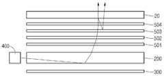
상기 광학 시트들(500)은 상기 도광판(200) 상에 배치된다. 상기 광학 시트들(500)은 상기 도광판(200)의 상면으로부터 출사되는 광의 특성을 변화 또는 향상시켜서, 상기 광을 상기 액정패널(20)에 공급한다.The
상기 광학 시트들(500)은 확산 시트(501), 제 1 프리즘 시트(502), 제 2 프리즘 시트(503) 및 광 변환 시트(504)일 수 있다.The
상기 확산 시트(501)는 상기 도광판(200) 상에 배치된다. 상기 확산 시트(501)는 통과되는 광의 균일도를 향상시킨다. 상기 확산 시트(501)는 다수 개의 비드들을 포함할 수 있다.The
상기 제 1 프리즘 시트(502)는 상기 확산 시트(501) 상에 배치된다. 상기 제 2 프리즘 시트(503)는 상기 제 1 프리즘 시트(502) 상에 배치된다. 상기 제 1 프리즘 시트(502) 및 상기 제 2 프리즘 시트(503)는 통과하는 광의 직진성을 증가시킨다.The
상기 광 변환 시트(504)는 상기 제 2 프리즘 시트(503) 상에 배치된다. 더 자세하게, 상기 광 변환 시트(504)는 상기 액정패널(20) 및 상기 제 2 프리즘 시트(503) 사이에 개재될 수 있다. 상기 광 변환 시트(504)는 입사되는 광의 파장을 변환하여 상방으로 출사할 수 있다.The
예를 들어, 상기 발광다이오드들(400)이 청색 발광다이오드인 경우, 상기 광 변환 시트(504)는 상기 도광판(200)으로부터 상방으로 출사되는 청색광을 녹색광 및 적색광으로 변환시킬 수 있다. 즉, 상기 광 변환 시트(504)는 상기 청색광의 일부를 약 520㎚ 내지 약 560㎚ 사이의 파장대를 가지는 녹색광으로 변환시키고, 상기 청색광의 다른 일부를 약 630㎚ 내지 약 660㎚ 사이의 파장대를 가지는 적색광으로 변환시킬 수 있다.For example, when the
또한, 상기 발광다이오드들(400)이 UV 발광다이오드인 경우, 상기 광 변환 시트(504)는 상기 도광판(200)의 상면으로부터 출사되는 자외선을 청색광, 녹색광 및 적색광으로 변환시킬 수 있다. 즉, 상기 광 변환 시트(504)는 상기 자외선의 일부를 약 430㎚ 내지 약 470㎚ 사이의 파장대를 가지는 청색광으로 변환시키고, 상기 자외선의 다른 일부를 약 520㎚ 내지 약 560㎚ 사이의 파장대를 가지는 녹색광으로 변환시키고, 상기 자외선의 또 다른 일부를 약 630㎚ 내지 약 660㎚ 사이의 파장대를 가지는 적색광으로 변환시킬 수 있다.In addition, when the
이에 따라서, 변환되지 않고 상기 광 변환 시트(504)를 통과하는 광 및 상기 광 변환 시트(504)에 의해서 변환된 광들은 백색광을 형성할 수 있다. 즉, 청색광, 녹색광 및 적색광이 조합되어, 상기 액정패널(20)에는 백색광이 입사될 수 있다.Accordingly, light passing through the
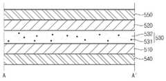
도 2 및 도 3에 도시된 바와 같이, 상기 광 변환 시트(504)는 하부 기판(510), 상부 기판(520), 파장 변환층(530), 하부 충격 흡수층(540) 및 상부 충격 흡수층(550)을 포함한다.2 and 3, the
상기 하부 기판(510)은 상기 파장 변환층(530) 아래에 배치된다. 상기 하부 기판(510)은 투명하며, 플렉서블 할 수 있다. 상기 하부 기판(510)은 상기 파장 변환층(530)의 하면에 밀착될 수 있다.The
상기 하부 기판(510)으로 사용되는 물질의 예로서는 폴리에틸렌테레프탈레이트(polyethyleneterephthalate;PET) 등과 같은 투명한 폴리머 등을 들 수 있다.Examples of the material used for the
상기 상부 기판(520)은 상기 파장 변환층(530) 상에 배치된다. 상기 상부 기판(520)은 투명하며, 플렉서블 할 수 있다. 상기 상부 기판(520)은 상기 파장 변환층(530)의 상면에 밀착될 수 있다.The
상기 상부 기판(520)으로 사용되는 물질의 예로서는 폴리에틸렌테레프탈레이트 등과 같은 투명한 폴리머 등을 들 수 있다.Examples of materials used for the
상기 하부 기판(510) 및 상기 상부 기판(520)은 상기 파장 변환층(530)을 샌드위치한다. 상기 하부 기판(510) 및 상기 상부 기판(520)은 상기 파장 변환층(530)을 지지한다. 상기 하부 기판(510) 및 상기 상부 기판(520)은 외부의 물리적인 충격으로부터 상기 파장 변환층(530)을 보호한다.The
또한, 상기 하부 기판(510) 및 상기 상부 기판(520)은 낮은 산소 투과도 및 투습성을 가진다. 이에 따라서, 상기 하부 기판(510) 및 상기 상부 기판(520)은 수분 및/또는 산소 등과 같은 외부의 화학적인 충격으로부터 상기 파장 변환층(530)을 보호할 수 있다.In addition, the
상기 파장 변환층(530)은 상기 하부 기판(510) 및 상기 상부 기판(520) 사이에 개재된다. 상기 파장 변환층(530)은 상기 하부 기판(510)의 상면에 밀착되고, 상기 상부 기판(520)의 하면에 밀착될 수 있다.The
상기 파장 변환층(530)은 다수 개의 광 변환 입자들(531) 및 호스트층(532)을 포함한다.The
상기 광 변환 입자들(531)은 상기 하부 기판(510) 및 상기 상부 기판(520) 사이에 배치된다. 더 자세하게, 상기 광 변환 입자들(531)은 상기 호스트층(532)에 균일하게 분산되고, 상기 호스트층(532)은 상기 하부 기판(510) 및 상기 상부 기판(520) 사이에 배치된다.The photo-
상기 광 변환 입자들(531)은 상기 발광다이오드들(400)로부터 출사되는 광의 파장을 변환시킨다. 상기 광 변환 입자들(531)은 상기 발광다이오드들(400)로부터 출사되는 광을 입사받아, 파장을 변환시킨다. 예를 들어, 상기 광 변환 입자들(531)은 상기 발광다이오드들(400)로부터 출사되는 청색광을 녹색광 및 적색광으로 변환시킬 수 있다. 즉, 상기 광 변환 입자들(531) 중 일부는 상기 청색광을 약 520㎚ 내지 약 560㎚ 사이의 파장대를 가지는 녹색광으로 변환시키고, 상기 광 변환 입자들(531) 중 다른 일부는 상기 청색광을 약 630㎚ 내지 약 660㎚ 사이의 파장대를 가지는 적색광으로 변환시킬 수 있다.The
이와는 다르게, 상기 광 변환 입자들(531)은 상기 발광다이오드들(400)로부터 출사되는 자외선을 청색광, 녹색광 및 적색광으로 변환시킬 수 있다. 즉, 상기 광 변환 입자들(531) 중 일부는 상기 자외선을 약 430㎚ 내지 약 470㎚ 사이의 파장대를 가지는 청색광으로 변환시키고, 상기 광 변환 입자들(531) 중 다른 일부는 상기 자외선을 약 520㎚ 내지 약 560㎚ 사이의 파장대를 가지는 녹색광으로 변환시킬 수 있다. 또한, 상기 광 변환 입자들(531) 중 또 다른 일부는 상기 자외선을 약 630㎚ 내지 약 660㎚ 사이의 파장대를 가지는 적색광으로 변환시킬 수 있다.Alternatively, the
즉, 상기 발광다이오드들(400)이 청색광을 발생시키는 청색 발광다이오드인 경우, 청색광을 녹색광 및 적색광으로 각각 변환시키는 광 변환 입자들(531)이 사용될 수 있다. 이와는 다르게, 상기 발광다이오드들(400)이 자외선을 발생시키는 UV 발광다이오드인 경우, 자외선을 청색광, 녹색광 및 적색광으로 각각 변환시키는 광 변환 입자들(531)이 사용될 수 있다.That is, when the
상기 광 변환 입자들(531)은 다수 개의 양자점(QD, Quantum Dot)들일 수 있다. 상기 양자점은 코어 나노 결정 및 상기 코어 나노 결정을 둘러싸는 껍질 나노 결정을 포함할 수 있다. 또한, 상기 양자점은 상기 껍질 나노 결정에 결합되는 유기 리간드를 포함할 수 있다. 또한, 상기 양자점은 상기 껍질 나노 결정을 둘러싸는 유기 코팅층을 포함할 수 있다.The
상기 껍질 나노 결정은 두 층 이상으로 형성될 수 있다. 상기 껍질 나노 결정은 상기 코어 나노 결정의 표면에 형성된다. 상기 양자점은 상기 코어 나오 결정으로 입광되는 빛의 파장을 껍질층을 형성하는 상기 껍질 나노 결정을 통해서 파장을 길게 변환시키고 빛의 효율을 증가시길 수 있다.The shell nanocrystals may be formed of two or more layers. The shell nanocrystals are formed on the surface of the core nanocrystals. The quantum dot may convert the wavelength of the light incident on the core core crystal into a long wavelength through the shell nanocrystals forming the shell layer and increase the light efficiency.
상기 양자점은 Ⅱ족 화합물 반도체, Ⅲ족 화합물 반도체, Ⅴ족 화합물 반도체 그리고 VI족 화합물 반도체 중에서 적어도 한가지 물질을 포함할 수 있다. 보다 상세하게, 상기 코어 나노 결정은 Cdse, InGaP, CdTe, CdS, ZnSe, ZnTe, ZnS, HgTe 또는 HgS를 포함할 수 있다. 또한, 상기 껍질 나노 결정은 CuZnS, CdSe, CdTe, CdS, ZnSe, ZnTe, ZnS, HgTe 또는 HgS를 포함할 수 있다. 상기 양자점의 지름은 1 nm 내지 10 nm일 수 있다.The quantum dot may include at least one of a group II compound semiconductor, a group III compound semiconductor, a group V compound semiconductor, and a group VI compound semiconductor. More specifically, the core nanocrystals may include Cdse, InGaP, CdTe, CdS, ZnSe, ZnTe, ZnS, HgTe or HgS. The shell nanocrystals may include CuZnS, CdSe, CdTe, CdS, ZnSe, ZnTe, ZnS, HgTe or HgS. The diameter of the quantum dot may be 1 nm to 10 nm.
상기 양자점에서 방출되는 빛의 파장은 상기 양자점의 크기 또는 합성 과정에서의 분자 클러스터 화합물(molecular cluster compound)와 나노입자 전구체 (precurser)의 몰분율 (molar ratio)에 따라 조절이 가능하다. 상기 유기 리간드는 피리딘(pyridine), 메르캅토 알콜(mercapto alcohol), 티올(thiol), 포스핀(phosphine) 및 포스핀 산화물(phosphine oxide) 등을 포함할 수 있다. 상기 유기 리간드는 합성 후 불안정한 양자점을 안정화시키는 역할을 한다. 합성 후에 댕글링 본드(dangling bond)가 외곽에 형성되며, 상기 댕글링 본드 때문에, 상기 양자점이 불안정해 질 수도 있다. 그러나, 상기 유기 리간드의 한 쪽 끝은 비결합 상태이고, 상기 비결합된 유기 리간드의 한 쪽 끝이 댕글링 본드와 결합해서, 상기 양자점을 안정화 시킬 수 있다.The wavelength of light emitted from the quantum dots can be controlled by the size of the quantum dots or the molar ratio of the molecular cluster compound and the nanoparticle precursor in the synthesis process. The organic ligand may include pyridine, mercapto alcohol, thiol, phosphine, phosphine oxide, and the like. The organic ligands serve to stabilize unstable quantum dots after synthesis. After synthesis, a dangling bond is formed on the outer periphery, and the quantum dots may become unstable due to the dangling bonds. However, one end of the organic ligand is in an unbonded state, and one end of the unbound organic ligand bonds with the dangling bond, thereby stabilizing the quantum dot.
특히, 상기 양자점은 그 크기가 빛, 전기 등에 의해 여기되는 전자와 정공이 이루는 엑시톤(exciton)의 보어 반경(Bohr raidus)보다 작게 되면 양자구속효과가 발생하여 띄엄띄엄한 에너지 준위를 가지게 되며 에너지 갭의 크기가 변화하게 된다. 또한, 전하가 양자점 내에 국한되어 높은 발광효율을 가지게 된다.Particularly, when the quantum dot has a size smaller than the Bohr radius of an exciton formed by electrons and holes excited by light, electricity or the like, a quantum confinement effect is generated to have a staggering energy level and an energy gap The size of the image is changed. Further, the charge is confined within the quantum dots, so that it has a high luminous efficiency.
이러한 상기 양자점은 일반적 형광 염료와 달리 입자의 크기에 따라 형광파장이 달라진다. 즉, 입자의 크기가 작아질수록 짧은 파장의 빛을 내며, 입자의 크기를 조절하여 원하는 파장의 가시광선영역의 형광을 낼 수 있다. 또한, 일반적 염료에 비해 흡광계수(extinction coefficient)가 100~1000배 크고 양자효율(quantum yield)도 높으므로 매우 센 형광을 발생한다.Unlike general fluorescent dyes, the quantum dots vary in fluorescence wavelength depending on the particle size. That is, as the size of the particle becomes smaller, it emits light having a shorter wavelength, and the particle size can be adjusted to produce fluorescence in a visible light region of a desired wavelength. In addition, since the extinction coefficient is 100 to 1000 times higher than that of a general dye, and the quantum yield is also high, it produces very high fluorescence.
상기 양자점은 화학적 습식방법에 의해 합성될 수 있다. 여기에서, 화학적 습식방법은 유기용매에 전구체 물질을 넣어 입자를 성장시키는 방법으로서, 화학적 습식방법에 의해서, 상기 양자점이 합성될 수 있다.The quantum dot can be synthesized by a chemical wet process. Here, the chemical wet method is a method of growing particles by adding a precursor material to an organic solvent, and the quantum dots can be synthesized by a chemical wet method.
상기 호스트층(532)은 상기 광 변환 입자들(531)을 둘러싼다. 즉, 상기 호스트층(532)은 상기 광 변환 입자들(531)을 균일하게 내부에 분산시킨다. 상기 호스트층(532)은 폴리머로 구성될 수 있다. 상기 호스트층(532)은 투명하다. 즉, 상기 호스트층(532)은 투명한 폴리머로 형성될 수 있다.The
상기 호스트층(532)은 상기 하부 기판(510) 및 상기 상부 기판(520) 사이에 배치된다. 상기 호스트층(532)은 상기 하부 기판(510)의 상면 및 상기 상부 기판(520)의 하면에 밀착될 수 있다.The
상기 하부 충격 흡수층(540)은 상기 파장 변환층(530) 아래에 배치된다. 더 자세하게, 상기 하부 충격 흡수층(540)은 상기 하부 기판(510) 아래에 배치될 수 있다. 더 자세하게, 상기 하부 충격 흡수층(540)은 상기 하부 기판(510)의 하면에 코팅될 수 있다.The lower
상기 하부 충격 흡수층(540)은 탄성을 가질 수 있다. 상기 하부 충격 흡수층(540)의 탄성 계수는 약 5.8N/㎠ 내지 약 6.6N/㎠ 일 수 있다. 또한, 상기 하부 충격 흡수층(540)의 두께는 약 100㎛ 내지 약 500㎛일 수 있다.The lower
상기 하부 충격 흡수층(540)은 약 5.8N/㎠ 내지 약 6.6N/㎠의 탄성 계수를 가질 때, 상기 광 변환 시트(501) 자체의 하중에 의한 충격을 효과적으로 흡수할 수 있다. 즉, 상기 하부 충격 흡수층(540)의 탄성 계수가 위와 같을 때, 상기 하부 충격 흡수층(540)은 상기 광 변환 시트(501)의 하중을 흡수하면서, 적당히 변형될 수 있다.When the lower
상기 하부 충격 흡수층(540)은 자가 복원 기능을 수행할 수 있다. 상기 하부 충격 흡수층(540)은 외부의 물리적인 충격에 의해서 일부가 눌리더라도, 다시 외형을 복원할 수 있다.The lower
이에 따라서, 상기 하부 충격 흡수층(540)은 높은 내스크래치 특성을 가질 수 있다. 또한, 상기 하부 충격 흡수층(540)은 아크릴계 수지 또는 우레탄계 수지를 포함할 수 있다.Accordingly, the lower
상기 하부 충격 흡수층(540)이 형성되기 위해서, 상기 하부 기판(510)의 하면에 아크릴계 수지 조성물 및/또는 우레탄계 수지 조성물이 코팅된다. 이때, 상기 수지 조성물이 코팅되기 위해서, 스프레이 코팅, 딥(dip) 코팅, 스핀 코팅, 슬롯(slot) 코팅, 슬릿(slit) 코팅, 바 코팅 및 롤투롤 코팅 등이 적용될 수 있다. 이후, 상기 코팅된 수지 조성물은 자외선 및/또는 열에 의해서 경화되고, 상기 하부 충격 흡수층(540)이 형성될 수 있다.In order to form the lower
상기 상부 충격 흡수층(550)은 상기 파장 변환층(530) 상에 배치된다. 더 자세하게, 상기 상부 충격 흡수층(550)은 상기 상부 기판(520) 상에 배치될 수 있다. 더 자세하게, 상기 상부 충격 흡수층(550)은 상기 상부 기판(520)의 상면에 코팅될 수 있다.The upper shock-absorbing
상기 상부 충격 흡수층(550)은 탄성을 가질 수 있다. 상기 상부 충격 흡수층(550)의 탄성 계수는 약 5.8N/㎠ 내지 약 6.6N/㎠ 일 수 있다. 또한, 상기 상부 충격 흡수층(550)의 두께는 약 100㎛ 내지 약 500㎛ 일 수 있다.The upper shock-absorbing
상기 상부 충격 흡수층(550)은 약 5.8N/㎠ 내지 약 6.6N/㎠의 탄성 계수를 가질 때, 상기 액정패널(20)의 하중에 의한 충격을 효과적으로 흡수할 수 있다. 즉, 상기 상부 충격 흡수층(550)의 탄성 계수가 위와 같을 때, 상기 상부 충격 흡수층(550)은 상기 액정패널(20)의 하중을 흡수하면서, 적당히 변형될 수 있다.When the upper shock-absorbing
상기 상부 충격 흡수층(550)은 자가 복원 기능을 수행할 수 있다. 상기 상부 충격 흡수층(550)은 외부의 물리적인 충격에 의해서 일부가 눌리더라도, 다시 외형을 복원할 수 있다.The upper
이에 따라서, 상기 상부 충격 흡수층(550)은 높은 내스크래치 특성을 가질 수 있다. 또한, 상기 상부 충격 흡수층(550)은 아크릴계 수지 또는 우레탄계 수지를 포함할 수 있다.Accordingly, the upper shock-absorbing
상기 상부 충격 흡수층(550)이 형성되기 위해서, 상기 상부 기판(520)의 상면에 아크릴계 수지 조성물 및/또는 우레탄계 수지 조성물이 코팅된다. 이후, 상기 코팅된 수지 조성물은 자외선 및/또는 열에 의해서 경화되고, 상기 하부 충격 흡수층(540)이 형성될 수 있다.In order to form the upper
상기 하부 충격 흡수층(540)은 상기 하부 기판(510)의 하면에 코팅된다. 또한, 상기 상부 충격 흡수층(550)은 상기 상부 기판(520)의 상면에 코팅된다. 이에 따라서, 상기 하부 충격 흡수층(540)은 상기 하부 기판(510)의 밀폐성을 향상시킬 수 있다. 또한, 상기 상부 충격 흡수층(550)도 상기 상부 기판(520)의 밀폐성을 향상시킬 수 있다.The lower
이에 따라서, 상기 하부 충격 흡수층(540) 및 상기 상부 충격 흡수층(550)은 외부의 습기 및/또는 산소로부터 상기 파장 변환층(530) 내의 광 변환 입자들(531)의 변성을 용이하게 방지할 수 있다.Accordingly, the lower
또한, 상기 하부 충격 흡수층(540)은 상기 하부 기판(510)보다 더 낮은 굴절율을 가질 수 있다. 또한, 상기 상부 충격 흡수층(550)은 상기 상부 기판(520)보다 더 낮은 굴절율을 가질 수 있다.In addition, the lower
이에 따라서, 상기 하부 충격 흡수층(540) 및 상기 상부 충격 흡수층(550)은 외부 광의 입사를 향상시키고, 외부로의 반사를 방지하는 반사 방지막 기능을 수행할 수 있다.Accordingly, the lower
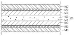
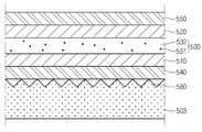
또한, 도 4에 도시된 바와 같이, 하부 충격 흡수층(540)은 파장 변환층(530)의 하면에 직접 배치될 수 있다. 즉, 상기 하부 충격 흡수층(540)은 상기 파장 변환층(530)의 하면에 직접 코팅될 수 있다.4, the lower
상부 충격 흡수층(550)도 상기 파장 변환층(530)의 상면에 직접 배치될 수 있다. 즉, 상기 상부 충격 흡수층(550)은 상기 파장 변환층(530)의 상면에 직접 코팅될 수 있다.The upper
또한, 도 5에 도시된 바와 같이, 하부 기판(510)의 하면에는 하부 반사 방지막(560)이 형성될 수 있다. 또한, 상기 하부 충격 흡수층(540)은 상기 하부 반사 방지막(560)의 하면에 직접 코팅되어 형성될 수 있다.5, a
상부 기판(520)의 상면에는 상부 반사 방지막(570)이 형성될 수 있다. 또한, 상기 상부 충격 흡수층(550)은 상기 상부 반사 방지막(570)의 상면에 직접 코팅되어 형성될 수 있다.An
상기 하부 반사 방지막(560) 및 상기 상부 반사 방지막(570)은 반사 방지 기능을 수행할 수 있다. 상기 하부 반사 방지막(560)은 상기 하부 기판(510)보다 낮은 굴절율을 가질 수 있고, 상기 상부 반사 방지막(570)은 상기 상부 기판(520)보다 낮은 굴절율을 가질 수 있다.The
또한, 상기 하부 충격 흡수층(540)의 굴절율은 상기 하부 반사 방지막(560)보다 더 낮을 수 있다. 상기 상부 충격 흡수층(550)의 굴절율은 상기 상부 반사 방지막(570)보다 더 낮을 수 있다.In addition, the refractive index of the lower
이에 따라서, 상기 하부 반사 방지막(560) 및 상기 상부 반사 방지막(570) 뿐만 아니라, 상기 하부 충격 흡수층(540) 및 상기 상부 충격 흡수층(550)에 의해서, 상기 파장 변환층(530)에 효과적으로 광이 입사될 수 있다.Accordingly, light is effectively transmitted to the
상기 액정패널(20)은 상기 광학시트들(500)상에 배치된다. 또한, 상기 액정패널(20)은 패널 가이드 상에 배치된다. 상기 액정패널(20)은 상기 패널 가이드에 의해서 가이드될 수 있다.The
상기 액정패널(20)은 통과하는 광의 세기를 조절하여 영상을 표시한다. 즉, 상기 액정패널(20)은 상기 백라이트 유닛(10)으로부터 출사되는 광을 사용하여, 영상을 표시하는 표시패널이다. 상기 액정패널(20)은 TFT기판(21), 컬러필터기판(22), 두 기판들 사이에 개재되는 액정층을 포함한다. 또한, 상기 액정패널(20)은 편광필터들을 포함한다.The
도면에는 상세히 도시되지 않았지만, 상기 TFT기판(21) 및 컬러필터기판(22)을 상세히 설명하면, 상기 TFT기판(21)은 복수의 게이트 라인 및 데이터 라인이 교차하여 화소를 정의하고, 각각의 교차영역마다 박막 트랜지스터(TFT : thin flim transistor)가 구비되어 각각의 픽셀에 실장된 화소전극과 일대일 대응되어 연결된다. 상기 컬러필터기판(22)은 각 픽셀에 대응되는 R, G, B 컬러의 컬러필터, 이들 각각을 테두리 하며 게이트 라인과 데이터 라인 및 박막 트랜지스터 등을 가리는 블랙 매트릭스와, 이들 모두를 덮는 공통전극을 포함한다.Although not shown in detail in the drawings, the
액정패널(21)의 가장자리에는 게이트 라인 및 데이터 라인으로 구동신호를 공급하는 구동 PCB(25)가 구비된다.A driving
상기 구동 PCB(25)는 COF(Chip on film, 24)에 의해 액정패널(21)과 전기적으로 연결된다. 여기서, 상기 COF(24)는 TCP(Tape Carrier Package)로 변경될 수 있다.The
상기 광 변환 시트(504)는 상기 광학 시트들(500) 중 최상부에 배치될 수 있다. 즉, 상기 광 변환 시트(504)는 다른 광학 시트들(500)을 덮을 수 있다. 이에 따라서, 상기 광 변환 시트(504)는 다른 광학 시트들(500)을 보호할 수 있다.The
구체적으로, 상기 바텀 커버(100) 내에 상기 도광판(200), 상기 반사시트(300), 상기 발광다이오드들(400), 상기 인쇄회로기판(401) 및 상기 광 변환 시트(504)을 제외한 광학 시트들(500)이 수용된다. 이후, 상기 광학 시트들(500) 상에 상기 광 변환 시트(504)가 적층되어, 상기 백라이트 유닛(10)이 조립된다.More specifically, the
이후, 상기 액정 패널을 조립하기 위한 공정에서, 상기 백라이트 유닛(10)은 이송될 수 있다. 이때, 상기 광 변환 시트(504)는 상기 상부 충격 흡수층(550)을 포함하기 때문에, 다른 광학 시트들(501, 502, 503)을 보호하면서, 동시에 자체적인 손상을 최소화할 수 있다.Then, in the process for assembling the liquid crystal panel, the
또한, 도 6에 도시된 바와 같이, 상기 제 2 프리즘 시트(503)는 상면에 다수 개의 피라미드 형상의 돌기 패턴(580)을 포함할 수 있다. 상기 돌기 패턴(580)은 상기 광 변환 시트(504)의 하면에 직접 접촉될 수 있다.Also, as shown in FIG. 6, the
이때, 상기 광 변환 시트(504)는 상기 하부 충격 흡수층(540)을 포함하기 때문에, 상기 돌기 패턴(580)에 의한 손상을 최소화할 수 있다. 이에 따라서, 실시예에 따른 액정표시장치는 외부 및 내부의 물리적인 충격에 의한 손상을 최소화할 수 있다. 따라서, 실시예에 따른 액정표시장치는 스크래치 등에 의한 화질 저하를 최소화할 수 있다.At this time, since the
또한, 상기 광 변환 시트(504)는 상하 방향으로 모두 반사 방지 기능을 수행하는 층들을 포함한다. 따라서, 도 7에 도시된 바와 같이, 변환되지 않고 상기 파장 변환층(530)을 통과한 광은 상기 액정패널(20)에 의해서 하방으로 반사될 수 있다. 이때, 하방으로 반사되는 광은 상기 상부 충격 흡수층(550) 및/또는 상기 상부 반사 방지막(570)에 의해서 효과적으로 상기 파장 변환층(530)에 입사될 수 있다.In addition, the
이와 같이, 더 많은 광이 상기 파장 변환층(530)에 입사되기 때문에, 상기 파장 변환층(530)의 변환 효율이 더 향상될 수 있다.As described above, since more light is incident on the
따라서, 상기 광 변환 시트(504)는 상기 발광다이오드들(400)로부터 출사되는 광의 파장을 효과적으로 변환시키고, 실시예에 따른 액정표시장치는 향상된 색재현성 및 휘도를 가질 수 있다.Accordingly, the
또한, 이상에서 실시예들에 설명된 특징, 구조, 효과 등은 본 발명의 적어도 하나의 실시예에 포함되며, 반드시 하나의 실시예에만 한정되는 것은 아니다. 나아가, 각 실시예에서 예시된 특징, 구조, 효과 등은 실시예들이 속하는 분야의 통상의 지식을 가지는 자에 의해 다른 실시예들에 대해서도 조합 또는 변형되어 실시 가능하다. 따라서 이러한 조합과 변형에 관계된 내용들은 본 발명의 범위에 포함되는 것으로 해석되어야 할 것이다.In addition, the features, structures, effects and the like described in the embodiments are included in at least one embodiment of the present invention, and are not necessarily limited to only one embodiment. Furthermore, the features, structures, effects and the like illustrated in the embodiments can be combined and modified by other persons skilled in the art to which the embodiments belong. Therefore, it should be understood that the present invention is not limited to these combinations and modifications.
이상에서 실시예를 중심으로 설명하였으나 이는 단지 예시일 뿐 본 발명을 한정하는 것이 아니며, 본 발명이 속하는 분야의 통상의 지식을 가진 자라면 본 실시예의 본질적인 특성을 벗어나지 않는 범위에서 이상에 예시되지 않은 여러 가지의 변형과 응용이 가능함을 알 수 있을 것이다. 예를 들어, 실시예에 구체적으로 나타난 각 구성 요소는 변형하여 실시할 수 있는 것이다. 그리고 이러한 변형과 응용에 관계된 차이점들은 첨부된 청구 범위에서 규정하는 본 발명의 범위에 포함되는 것으로 해석되어야 할 것이다.While the present invention has been particularly shown and described with reference to exemplary embodiments thereof, it is to be understood that the invention is not limited to the disclosed exemplary embodiments, but, on the contrary, It will be understood that various modifications and applications are possible. For example, each component specifically shown in the embodiments can be modified and implemented. It is to be understood that all changes and modifications that come within the meaning and range of equivalency of the claims are therefore intended to be embraced therein.
Claims (12)
Translated fromKorean상기 도광판의 측면 상에 배치되는 광원;
상기 도광판의 하부에 배치되는 반사시트;
상기 도광판의 상부에 배치되는 확산시트;
상기 확산 시트 상에 배치되는 프리즘 시트; 및
상기 프리즘 시트 상에 배치되는 광 변환 시트를 포함하고,
상기 광 변환 시트는,
하부 기판;
상기 하부 기판의 하부 상에 배치되는 하부 충격 흡수층;
상기 하부 기판의 상부 상에 배치되는 파장 변환층;
상기 파장 변환층 상의 상부 기판; 및
상기 상부 기판의 상부 상에 배치되는 상부 충격 흡수층을 포함하고,
상기 파장 변환층은 호스트층 및 상기 호스트층에 분산되는 복수의 양자점들을 포함하고,
상기 하부 충격 흡수층 및 상기 상부 충격 흡수층의 탄성 계수는 5.8N/㎠ 내지 6.6N/㎠이고,
상기 하부 충격 흡수층 및 상기 상부 충격 흡수층의 두께는 100㎛ 내지 500㎛이고,
상기 하부 충격 흡수층은 상기 하부 기판보다 낮은 굴절율을 가지고,
상기 상부 충격 흡수층은 상기 상부 기판보다 낮은 굴절율을 가지는 백라이트 유닛.A light guide plate;
A light source disposed on a side surface of the light guide plate;
A reflective sheet disposed under the light guide plate;
A diffusion sheet disposed on the light guide plate;
A prism sheet disposed on the diffusion sheet; And
And a light conversion sheet disposed on the prism sheet,
The light-
A lower substrate;
A lower shock absorbing layer disposed on a lower portion of the lower substrate;
A wavelength conversion layer disposed on an upper portion of the lower substrate;
An upper substrate on the wavelength conversion layer; And
And an upper shock absorbing layer disposed on an upper portion of the upper substrate,
Wherein the wavelength conversion layer includes a host layer and a plurality of quantum dots dispersed in the host layer,
The elastic modulus of the lower impact absorbing layer and the upper impact absorbing layer is 5.8 N / cm2 to 6.6 N /
The thickness of the lower impact-absorbing layer and the upper shock-absorbing layer is 100 탆 to 500 탆,
Wherein the lower shock absorbing layer has a refractive index lower than that of the lower substrate,
Wherein the upper shock absorbing layer has a refractive index lower than that of the upper substrate.
상기 하부 충격 흡수층은 상기 하부 기판과 직접 접촉하며 배치되고,
상기 상부 충격 흡수층은 상기 상부 기판과 직접 접촉하며 배치되는 백라이트 유닛.The method according to claim 1,
Wherein the lower shock absorbing layer is disposed in direct contact with the lower substrate,
Wherein the upper shock absorbing layer is disposed in direct contact with the upper substrate.
상기 하부 충격 흡수층 및 상기 상부 충격 흡수층은 아크릴계 수지 또는 우레탄계 수지를 포함하는 백라이트 유닛.The method according to claim 1,
Wherein the lower impact absorbing layer and the upper impact absorbing layer comprise acrylic resin or urethane resin.
상기 광 변환 시트는 상기 프리즘 시트를 덮으면서 배치되는 백라이트 유닛.The method according to claim 1,
Wherein the light conversion sheet is disposed while covering the prism sheet.
상기 프리즘 시트는 상기 확산 시트 상의 제 1 프리즘 시트 및 상기 제 1 프리즘 시트 상의 제 2 프리즘 시트를 포함하고,
상기 제 2 프리즘 시트의 상면 상에는 상기 광 변환 시트의 상기 하부 충격 흡수층의 하면과 직접 접촉하며 배치되는 돌기 패턴을 포함하는 백라이트 유닛.The method according to claim 1,
Wherein the prism sheet includes a first prism sheet on the diffusion sheet and a second prism sheet on the first prism sheet,
And a projection pattern disposed on the upper surface of the second prism sheet in direct contact with the lower surface of the lower impact absorbing layer of the light conversion sheet.
상기 도광판의 측면 상에 배치되는 광원;
상기 도광판의 하부에 배치되는 반사시트;
상기 도광판의 상부에 배치되는 확산시트;
상기 확산 시트 상에 배치되는 프리즘 시트;
상기 프리즘 시트 상에 배치되는 광 변환 시트; 및
상기 광 변환 시트 상에 배치되는 액정 패널을 포함하고,
상기 광 변환 시트는,
하부 기판;
상기 하부 기판의 하부 상에 배치되는 하부 충격 흡수층;
상기 하부 기판의 상부 상에 배치되는 파장 변환층;
상기 파장 변환층 상의 상부 기판; 및
상기 상부 기판의 상부 상에 배치되는 상부 충격 흡수층을 포함하고,
상기 파장 변환층은 호스트층 및 상기 호스트층에 분산되는 복수의 양자점들을 포함하고,
상기 하부 충격 흡수층 및 상기 상부 충격 흡수층의 탄성 계수는 5.8N/㎠ 내지 6.6N/㎠이고,
상기 하부 충격 흡수층 및 상기 상부 충격 흡수층의 두께는 100㎛ 내지 500㎛이고,
상기 하부 충격 흡수층은 상기 하부 기판보다 낮은 굴절율을 가지고,
상기 상부 충격 흡수층은 상기 상부 기판보다 낮은 굴절율을 가지는 표시 장치.A light guide plate;
A light source disposed on a side surface of the light guide plate;
A reflective sheet disposed under the light guide plate;
A diffusion sheet disposed on the light guide plate;
A prism sheet disposed on the diffusion sheet;
A light conversion sheet disposed on the prism sheet; And
And a liquid crystal panel disposed on the light conversion sheet,
The light-
A lower substrate;
A lower shock absorbing layer disposed on a lower portion of the lower substrate;
A wavelength conversion layer disposed on an upper portion of the lower substrate;
An upper substrate on the wavelength conversion layer; And
And an upper shock absorbing layer disposed on an upper portion of the upper substrate,
Wherein the wavelength conversion layer includes a host layer and a plurality of quantum dots dispersed in the host layer,
The elastic modulus of the lower impact absorbing layer and the upper impact absorbing layer is 5.8 N / cm2 to 6.6 N /
The thickness of the lower impact-absorbing layer and the upper shock-absorbing layer is 100 탆 to 500 탆,
Wherein the lower shock absorbing layer has a refractive index lower than that of the lower substrate,
Wherein the upper shock absorbing layer has a refractive index lower than that of the upper substrate.
상기 하부 충격 흡수층은 상기 하부 기판과 직접 접촉하며 배치되고,
상기 상부 충격 흡수층은 상기 상부 기판과 직접 접촉하며 배치되는 표시장치.The method according to claim 6,
Wherein the lower shock absorbing layer is disposed in direct contact with the lower substrate,
Wherein the upper shock absorbing layer is disposed in direct contact with the upper substrate.
상기 광 변환 시트는 상기 프리즘 시트를 덮으면서 배치되는 표시장치.The method according to claim 6,
And the light conversion sheet is disposed while covering the prism sheet.
상기 프리즘 시트는 상기 확산 시트 상의 제 1 프리즘 시트 및 상기 제 1 프리즘 시트 상의 제 2 프리즘 시트를 포함하고,
상기 제 2 프리즘 시트의 상면 상에는 상기 광 변환 시트의 상기 하부 충격 흡수층의 하면과 직접 접촉하며 배치되는 돌기 패턴을 포함하는 표시 장치.The method according to claim 6,
Wherein the prism sheet includes a first prism sheet on the diffusion sheet and a second prism sheet on the first prism sheet,
And a protrusion pattern disposed on the upper surface of the second prism sheet in direct contact with a lower surface of the lower impact absorbing layer of the light conversion sheet.
상기 하부 충격 흡수층 및 상기 상부 충격 흡수층은 아크릴계 수지 또는 우레탄계 수지를 포함하는 표시장치.The method according to claim 6,
Wherein the lower impact absorbing layer and the upper impact absorbing layer comprise an acrylic resin or a urethane resin.
상기 하부 기판 및 상기 상부 기판은 폴리에틸렌테레프탈레이트를 포함하는 표시장치.The method according to claim 6,
Wherein the lower substrate and the upper substrate comprise polyethylene terephthalate.
상기 하부 충격 흡수층은 상기 하부 기판 및 상기 프리즘 시트 사이에 배치되고,
상기 상부 충격 흡수층은 상기 상부 기판 및 상기 액정 패널 사이에 배치되는 표시 장치.The method according to claim 6,
Wherein the lower shock absorbing layer is disposed between the lower substrate and the prism sheet,
And the upper shock absorbing layer is disposed between the upper substrate and the liquid crystal panel.
Priority Applications (6)
| Application Number | Priority Date | Filing Date | Title |
|---|---|---|---|
| KR1020110034472AKR101905852B1 (en) | 2011-04-13 | 2011-04-13 | Optical sheet and display device having the same |
| US14/111,421US9140837B2 (en) | 2011-04-13 | 2011-11-30 | Optical member and display device including the same |
| PCT/KR2011/009235WO2012141401A1 (en) | 2011-04-13 | 2011-11-30 | Optical member and display device including the same |
| TW100146036ATWI582498B (en) | 2011-04-13 | 2011-12-13 | Optical member and display device including the same |
| US14/830,440US9599314B2 (en) | 2011-04-13 | 2015-08-19 | Optical member and display device including the same |
| US15/415,623US10215366B2 (en) | 2011-04-13 | 2017-01-25 | Optical member and display device including the same |
Applications Claiming Priority (1)
| Application Number | Priority Date | Filing Date | Title |
|---|---|---|---|
| KR1020110034472AKR101905852B1 (en) | 2011-04-13 | 2011-04-13 | Optical sheet and display device having the same |
Publications (2)
| Publication Number | Publication Date |
|---|---|
| KR20120116815A KR20120116815A (en) | 2012-10-23 |
| KR101905852B1true KR101905852B1 (en) | 2018-10-08 |
Family
ID=47009536
Family Applications (1)
| Application Number | Title | Priority Date | Filing Date |
|---|---|---|---|
| KR1020110034472AActiveKR101905852B1 (en) | 2011-04-13 | 2011-04-13 | Optical sheet and display device having the same |
Country Status (4)
| Country | Link |
|---|---|
| US (3) | US9140837B2 (en) |
| KR (1) | KR101905852B1 (en) |
| TW (1) | TWI582498B (en) |
| WO (1) | WO2012141401A1 (en) |
Families Citing this family (16)
| Publication number | Priority date | Publication date | Assignee | Title |
|---|---|---|---|---|
| US8960977B2 (en) | 2012-08-10 | 2015-02-24 | Lg Innotek Co., Ltd. | Illuminating device |
| EP2696135B1 (en)* | 2012-08-10 | 2019-11-27 | LG Innotek Co., Ltd. | Lighting device |
| JP6119490B2 (en)* | 2013-07-31 | 2017-04-26 | ソニー株式会社 | Light source device and display device |
| KR102260013B1 (en)* | 2014-12-10 | 2021-06-04 | 삼성디스플레이 주식회사 | Display apparatus and method of manufacturing the same |
| US20160224973A1 (en)* | 2015-02-01 | 2016-08-04 | Apple Inc. | User interface for payments |
| EP3273143A4 (en)* | 2015-03-18 | 2018-11-07 | Sharp Kabushiki Kaisha | Illumination device, display device, and television receiving device |
| WO2016158371A1 (en)* | 2015-04-01 | 2016-10-06 | シャープ株式会社 | Illumination device, display device, and television reception device |
| CN104950518A (en)* | 2015-07-21 | 2015-09-30 | 京东方科技集团股份有限公司 | Quantum dot film, preparation method thereof, and backlight module |
| DE102017205943B4 (en) | 2016-04-08 | 2022-08-04 | GM Global Technology Operations LLC | Compliant light emitting display assembly |
| KR102186854B1 (en)* | 2016-10-27 | 2020-12-04 | 삼성전자주식회사 | Display apparatus and display panel for the same |
| JP6919269B2 (en)* | 2017-03-29 | 2021-08-18 | セイコーエプソン株式会社 | Light source device and projector |
| JP2018197782A (en)* | 2017-05-23 | 2018-12-13 | Dic株式会社 | Light conversion film and liquid crystal display element using the same |
| KR102459728B1 (en)* | 2017-10-20 | 2022-10-31 | 삼성디스플레이 주식회사 | Liquid crystal display panel and liquid crystal display device including the same |
| CN111367103B (en)* | 2018-12-25 | 2023-03-14 | 群创光电股份有限公司 | Display device and method for manufacturing the same |
| TWI737269B (en)* | 2020-04-20 | 2021-08-21 | 光耀科技股份有限公司 | Backlight module |
| TWI807323B (en)* | 2021-05-17 | 2023-07-01 | 勝智會科技顧問股份有限公司 | Display structure having a laser light wavelength conversion layer |
Citations (3)
| Publication number | Priority date | Publication date | Assignee | Title |
|---|---|---|---|---|
| JP2002309199A (en) | 2001-04-16 | 2002-10-23 | Sharp Corp | Adhesive sheet, laminated sheet and liquid crystal display |
| JP2006010748A (en)* | 2004-06-22 | 2006-01-12 | Seiko Epson Corp | Optical sheet, electro-optical device, electronic apparatus, and optical sheet manufacturing method |
| JP2009522602A (en) | 2005-12-30 | 2009-06-11 | スリーエム イノベイティブ プロパティズ カンパニー | Strongly reflective polarizing film |
Family Cites Families (28)
| Publication number | Priority date | Publication date | Assignee | Title |
|---|---|---|---|---|
| CA2162451A1 (en)* | 1994-12-22 | 1996-06-23 | John P. Murphy | Anti-reflective clarifier film for eyeglasses |
| WO1996038757A1 (en)* | 1995-06-02 | 1996-12-05 | Matsushita Electric Industrial Co., Ltd. | Optical device, laser beam source, laser apparatus and method of producing optical device |
| EP0962789B1 (en)* | 1998-06-05 | 2008-02-06 | FUJIFILM Corporation | Anti-reflection film and display device having the same |
| JP4854892B2 (en)* | 1999-06-17 | 2012-01-18 | 富士フイルム株式会社 | Image display device with optical filter |
| JP2002182003A (en)* | 2000-12-14 | 2002-06-26 | Canon Inc | Anti-reflection function element, optical element, optical system and optical equipment |
| US7800121B2 (en)* | 2002-08-30 | 2010-09-21 | Lumination Llc | Light emitting diode component |
| JP2005234476A (en)* | 2004-02-23 | 2005-09-02 | Fuji Photo Film Co Ltd | Antireflection coating, antireflection film and image display apparatus |
| EP1735645B1 (en)* | 2004-04-14 | 2012-08-15 | LG Chem, Ltd. | Anti-reflective coating composition and coating film with excellent stain resistance |
| KR20060000544A (en)* | 2004-06-29 | 2006-01-06 | 삼성전자주식회사 | Backlight for display device, Light source for display device, Light emitting diode for light source |
| US7440044B2 (en)* | 2004-11-29 | 2008-10-21 | Arisawa Manufacturing Co., Ltd. | Color display device and method |
| TWI419375B (en)* | 2005-02-18 | 2013-12-11 | Nichia Corp | Light-emitting device with lens for controlling light distribution characteristics |
| TWI345105B (en)* | 2006-01-26 | 2011-07-11 | Chimei Innolux Corp | Backlight module and application thereof |
| KR100891008B1 (en)* | 2006-12-20 | 2009-03-31 | (주)케이디티 | Flat panel lighting equipment |
| KR20080057856A (en) | 2006-12-21 | 2008-06-25 | 삼성전자주식회사 | Inkjet Jetting Device and Method |
| US7963677B2 (en)* | 2006-12-28 | 2011-06-21 | Seiko Epson Corporation | Light source device, having wavelength conversion and separation means, and projector |
| KR20080063986A (en)* | 2007-01-03 | 2008-07-08 | 삼성전기주식회사 | Diffusion sheet for wavelength conversion and backlight unit using the same |
| JP2008191649A (en)* | 2007-01-12 | 2008-08-21 | Seiko Epson Corp | Laser light source device, illumination device, image display device, and monitor device |
| US8179034B2 (en)* | 2007-07-13 | 2012-05-15 | 3M Innovative Properties Company | Light extraction film for organic light emitting diode display and lighting devices |
| JP4613947B2 (en)* | 2007-12-07 | 2011-01-19 | ソニー株式会社 | Illumination device, color conversion element, and display device |
| JP5193586B2 (en)* | 2007-12-25 | 2013-05-08 | 株式会社東芝 | Semiconductor light emitting device |
| US8411228B2 (en)* | 2008-03-07 | 2013-04-02 | Sharp Kabushiki Kaisha | Light emitting module, backlight unit and liquid crystal display device |
| US7957621B2 (en)* | 2008-12-17 | 2011-06-07 | 3M Innovative Properties Company | Light extraction film with nanoparticle coatings |
| US20110044359A1 (en)* | 2009-08-18 | 2011-02-24 | Douglas Llewellyn Butler | Intracavity Conversion Utilizing Narrow Band Reflective SOA |
| US7977637B1 (en)* | 2009-08-20 | 2011-07-12 | Hrl Laboratories, Llc | Honeycomb infrared detector |
| JP5366765B2 (en)* | 2009-11-10 | 2013-12-11 | 日東電工株式会社 | Polarizing plate and image display device |
| TW201145597A (en)* | 2010-01-28 | 2011-12-16 | Lg Innotek Co Ltd | Light emitting device package |
| WO2011141779A1 (en)* | 2010-05-12 | 2011-11-17 | Oree, Advanced Illumination Solutions Inc. | Illumination apparatus with high conversion efficiency and methods of forming the same |
| KR101184434B1 (en)* | 2010-12-15 | 2012-09-20 | 한국과학기술연구원 | Color conversion luminescent sheet and the fabrication method thereof |
- 2011
- 2011-04-13KRKR1020110034472Apatent/KR101905852B1/enactiveActive
- 2011-11-30USUS14/111,421patent/US9140837B2/enactiveActive
- 2011-11-30WOPCT/KR2011/009235patent/WO2012141401A1/enactiveApplication Filing
- 2011-12-13TWTW100146036Apatent/TWI582498B/enactive
- 2015
- 2015-08-19USUS14/830,440patent/US9599314B2/enactiveActive
- 2017
- 2017-01-25USUS15/415,623patent/US10215366B2/enactiveActive
Patent Citations (3)
| Publication number | Priority date | Publication date | Assignee | Title |
|---|---|---|---|---|
| JP2002309199A (en) | 2001-04-16 | 2002-10-23 | Sharp Corp | Adhesive sheet, laminated sheet and liquid crystal display |
| JP2006010748A (en)* | 2004-06-22 | 2006-01-12 | Seiko Epson Corp | Optical sheet, electro-optical device, electronic apparatus, and optical sheet manufacturing method |
| JP2009522602A (en) | 2005-12-30 | 2009-06-11 | スリーエム イノベイティブ プロパティズ カンパニー | Strongly reflective polarizing film |
Also Published As
| Publication number | Publication date |
|---|---|
| KR20120116815A (en) | 2012-10-23 |
| US20170131453A1 (en) | 2017-05-11 |
| US9140837B2 (en) | 2015-09-22 |
| US10215366B2 (en) | 2019-02-26 |
| US9599314B2 (en) | 2017-03-21 |
| US20140029239A1 (en) | 2014-01-30 |
| US20150354784A1 (en) | 2015-12-10 |
| WO2012141401A1 (en) | 2012-10-18 |
| TW201241519A (en) | 2012-10-16 |
| TWI582498B (en) | 2017-05-11 |
Similar Documents
| Publication | Publication Date | Title |
|---|---|---|
| KR101905852B1 (en) | Optical sheet and display device having the same | |
| KR101210163B1 (en) | Optical sheet and method of fabricating the same | |
| KR101673627B1 (en) | Optical member and display device | |
| KR101251815B1 (en) | Optical sheet and display device having the same | |
| KR101664507B1 (en) | Display device | |
| KR20120119547A (en) | Optical member and method for fabricating the same | |
| KR101725023B1 (en) | Optical member and display device | |
| KR20120107794A (en) | Light conversion member and display device having the same | |
| KR101855991B1 (en) | Display device | |
| KR101326938B1 (en) | Optical member and display device having the same | |
| KR101251807B1 (en) | Display device | |
| KR101792882B1 (en) | Optical member and method of fabricating the same | |
| KR101210173B1 (en) | Display device | |
| KR101956058B1 (en) | Display device | |
| KR101210084B1 (en) | Optical member and method of fabricating the same | |
| KR101262502B1 (en) | Optical member and display device having the same | |
| KR101210068B1 (en) | Optical member, display device having the same and method of fabricating the same | |
| KR101882199B1 (en) | Optical member, display device having the same and method of fabricating the same | |
| KR101877489B1 (en) | Display | |
| KR101814809B1 (en) | Display device | |
| KR101283130B1 (en) | Display device | |
| KR101251775B1 (en) | Optical member, display device having the same and method of fabricating the same | |
| KR101360638B1 (en) | Display, light conversion member and method of fabricating light conversion member | |
| KR101812338B1 (en) | Optical member and display device having the same and method of fabricating the same | |
| KR101725012B1 (en) | Display device |
Legal Events
| Date | Code | Title | Description |
|---|---|---|---|
| PA0109 | Patent application | Patent event code:PA01091R01D Comment text:Patent Application Patent event date:20110413 | |
| PG1501 | Laying open of application | ||
| A201 | Request for examination | ||
| PA0201 | Request for examination | Patent event code:PA02012R01D Patent event date:20160217 Comment text:Request for Examination of Application Patent event code:PA02011R01I Patent event date:20110413 Comment text:Patent Application | |
| E902 | Notification of reason for refusal | ||
| PE0902 | Notice of grounds for rejection | Comment text:Notification of reason for refusal Patent event date:20171027 Patent event code:PE09021S01D | |
| E90F | Notification of reason for final refusal | ||
| PE0902 | Notice of grounds for rejection | Comment text:Final Notice of Reason for Refusal Patent event date:20180424 Patent event code:PE09021S02D | |
| E701 | Decision to grant or registration of patent right | ||
| PE0701 | Decision of registration | Patent event code:PE07011S01D Comment text:Decision to Grant Registration Patent event date:20180717 | |
| GRNT | Written decision to grant | ||
| PR0701 | Registration of establishment | Comment text:Registration of Establishment Patent event date:20181001 Patent event code:PR07011E01D | |
| PR1002 | Payment of registration fee | Payment date:20181002 End annual number:3 Start annual number:1 | |
| PG1601 | Publication of registration | ||
| PR1001 | Payment of annual fee | Payment date:20210913 Start annual number:4 End annual number:4 | |
| PR1001 | Payment of annual fee | Payment date:20230912 Start annual number:6 End annual number:6 | |
| PR1001 | Payment of annual fee |