KR101903671B1 - Thin film transistor array panel and manufacturing method thereof - Google Patents
Thin film transistor array panel and manufacturing method thereofDownload PDFInfo
- Publication number
- KR101903671B1 KR101903671B1KR1020110102550AKR20110102550AKR101903671B1KR 101903671 B1KR101903671 B1KR 101903671B1KR 1020110102550 AKR1020110102550 AKR 1020110102550AKR 20110102550 AKR20110102550 AKR 20110102550AKR 101903671 B1KR101903671 B1KR 101903671B1
- Authority
- KR
- South Korea
- Prior art keywords
- electrode
- contact hole
- semiconductor layer
- layer
- thin film
- Prior art date
- Legal status (The legal status is an assumption and is not a legal conclusion. Google has not performed a legal analysis and makes no representation as to the accuracy of the status listed.)
- Active
Links
- 239000010409thin filmSubstances0.000titleclaimsabstractdescription48
- 238000004519manufacturing processMethods0.000titleclaimsabstractdescription26
- 239000010408filmSubstances0.000claimsabstractdescription81
- 239000004065semiconductorSubstances0.000claimsabstractdescription79
- 239000000758substrateSubstances0.000claimsabstractdescription33
- 238000000034methodMethods0.000claimsabstractdescription27
- 229910021420polycrystalline siliconInorganic materials0.000claimsabstractdescription6
- 239000002184metalSubstances0.000claimsdescription65
- 229920002120photoresistant polymerPolymers0.000claimsdescription43
- 239000011810insulating materialSubstances0.000claimsdescription16
- 238000005530etchingMethods0.000claimsdescription15
- 238000004380ashingMethods0.000claimsdescription6
- 238000000059patterningMethods0.000claimsdescription4
- MYMOFIZGZYHOMD-UHFFFAOYSA-NDioxygenChemical compoundO=OMYMOFIZGZYHOMD-UHFFFAOYSA-N0.000claimsdescription3
- 229910001882dioxygenInorganic materials0.000claimsdescription3
- 239000012535impuritySubstances0.000claimsdescription2
- 238000009413insulationMethods0.000claims1
- 239000010410layerSubstances0.000description177
- 239000000463materialSubstances0.000description4
- 229910021417amorphous siliconInorganic materials0.000description3
- 230000000694effectsEffects0.000description3
- 239000007769metal materialSubstances0.000description3
- 238000010586diagramMethods0.000description2
- 238000001312dry etchingMethods0.000description2
- 238000000137annealingMethods0.000description1
- 239000011521glassSubstances0.000description1
- 238000010438heat treatmentMethods0.000description1
- 150000002500ionsChemical class0.000description1
- 239000004973liquid crystal related substanceSubstances0.000description1
- 229910052755nonmetalInorganic materials0.000description1
- 239000002356single layerSubstances0.000description1
Images


Classifications
- H—ELECTRICITY
- H10—SEMICONDUCTOR DEVICES; ELECTRIC SOLID-STATE DEVICES NOT OTHERWISE PROVIDED FOR
- H10D—INORGANIC ELECTRIC SEMICONDUCTOR DEVICES
- H10D86/00—Integrated devices formed in or on insulating or conducting substrates, e.g. formed in silicon-on-insulator [SOI] substrates or on stainless steel or glass substrates
- H10D86/40—Integrated devices formed in or on insulating or conducting substrates, e.g. formed in silicon-on-insulator [SOI] substrates or on stainless steel or glass substrates characterised by multiple TFTs
- H10D86/441—Interconnections, e.g. scanning lines
- H—ELECTRICITY
- H10—SEMICONDUCTOR DEVICES; ELECTRIC SOLID-STATE DEVICES NOT OTHERWISE PROVIDED FOR
- H10D—INORGANIC ELECTRIC SEMICONDUCTOR DEVICES
- H10D30/00—Field-effect transistors [FET]
- H10D30/01—Manufacture or treatment
- H10D30/021—Manufacture or treatment of FETs having insulated gates [IGFET]
- H10D30/031—Manufacture or treatment of FETs having insulated gates [IGFET] of thin-film transistors [TFT]
- H10D30/0312—Manufacture or treatment of FETs having insulated gates [IGFET] of thin-film transistors [TFT] characterised by the gate electrodes
- H10D30/0316—Manufacture or treatment of FETs having insulated gates [IGFET] of thin-film transistors [TFT] characterised by the gate electrodes of lateral bottom-gate TFTs comprising only a single gate
- H—ELECTRICITY
- H10—SEMICONDUCTOR DEVICES; ELECTRIC SOLID-STATE DEVICES NOT OTHERWISE PROVIDED FOR
- H10D—INORGANIC ELECTRIC SEMICONDUCTOR DEVICES
- H10D30/00—Field-effect transistors [FET]
- H10D30/60—Insulated-gate field-effect transistors [IGFET]
- H10D30/67—Thin-film transistors [TFT]
- H10D30/6729—Thin-film transistors [TFT] characterised by the electrodes
- H—ELECTRICITY
- H10—SEMICONDUCTOR DEVICES; ELECTRIC SOLID-STATE DEVICES NOT OTHERWISE PROVIDED FOR
- H10D—INORGANIC ELECTRIC SEMICONDUCTOR DEVICES
- H10D86/00—Integrated devices formed in or on insulating or conducting substrates, e.g. formed in silicon-on-insulator [SOI] substrates or on stainless steel or glass substrates
- H10D86/01—Manufacture or treatment
- H10D86/021—Manufacture or treatment of multiple TFTs
- H10D86/0231—Manufacture or treatment of multiple TFTs using masks, e.g. half-tone masks
- H—ELECTRICITY
- H10—SEMICONDUCTOR DEVICES; ELECTRIC SOLID-STATE DEVICES NOT OTHERWISE PROVIDED FOR
- H10D—INORGANIC ELECTRIC SEMICONDUCTOR DEVICES
- H10D86/00—Integrated devices formed in or on insulating or conducting substrates, e.g. formed in silicon-on-insulator [SOI] substrates or on stainless steel or glass substrates
- H10D86/40—Integrated devices formed in or on insulating or conducting substrates, e.g. formed in silicon-on-insulator [SOI] substrates or on stainless steel or glass substrates characterised by multiple TFTs
- H10D86/60—Integrated devices formed in or on insulating or conducting substrates, e.g. formed in silicon-on-insulator [SOI] substrates or on stainless steel or glass substrates characterised by multiple TFTs wherein the TFTs are in active matrices
Landscapes
- Liquid Crystal (AREA)
- Thin Film Transistor (AREA)
Abstract
Translated fromKoreanDescription
Translated fromKorean본 발명은 박막 트랜지스터 표시판 및 그 제조 방법에 관한 것으로, 보다 상세하게는 마스크의 오정렬로 인해 배선이 끊어지는 것을 방지할 수 있고, 사용되는 마스크의 수를 줄여 공정을 단순하게 하고 비용을 줄일 수 있는 박막 트랜지스터 표시판 및 그 제조 방법에 관한 것이다.The present invention relates to a thin film transistor panel and a method of manufacturing the same, and more particularly, to a thin film transistor panel and a method of manufacturing the same, A thin film transistor panel, and a method of manufacturing the same.
일반적으로 박막 트랜지스터(thin film transistor, TFT)는 액정 표시 장치나 유기 발광 표시 장치(organic light emitting display) 등의 평판 표시 장치에서 각 화소를 독립적으로 구동하기 위한 스위칭 소자로 사용된다. 박막 트랜지스터를 포함하는 박막 트랜지스터 표시판은 박막 트랜지스터와 이에 연결되어 있는 화소 전극, 박막 트랜지스터에 게이트 신호를 전달하는 게이트선과 데이터 신호를 전달하는 데이터선 등을 포함한다.In general, a thin film transistor (TFT) is used as a switching element for independently driving each pixel in a flat panel display device such as a liquid crystal display device or an organic light emitting display. A thin film transistor panel including a thin film transistor includes a thin film transistor, a pixel electrode connected to the thin film transistor, a gate line for transmitting a gate signal to the thin film transistor, and a data line for transmitting a data signal.
박막 트랜지스터는 반도체층, 게이트선에 연결되어 반도체층 위에 형성되는 게이트 전극, 데이터선에 연결되어 있는 소스 전극, 화소 전극에 연결되어 있는 드레인 전극 등을 포함하여 이루어지며, 게이트선을 통해 전달되는 게이트 신호에 따라 데이터선을 통해 전달되는 데이터 신호를 화소 전극에 전달한다.The thin film transistor includes a semiconductor layer, a gate electrode connected to the gate line and formed on the semiconductor layer, a source electrode connected to the data line, a drain electrode connected to the pixel electrode, and the like. And transmits the data signal transmitted through the data line to the pixel electrode according to the signal.
이러한 박막 트랜지스터 표시판은 기판 위에 금속층 등을 형성하고, 마스크를 정렬시켜, 복수의 포토 및 식각 공정을 진행함으로써 형성된다. 첫 번째 마스크를 기판 위에 정렬 시켜 포토 및 식각 공정을 진행한 후, 두 번째 마스크를 첫 번째 마스크와 동일하게 정렬 시켜 포토 및 식각 공정을 진행한다. 이때, 두 번째 마스크를 첫 번째 마스크와 어긋나도록 정렬 시킨 경우 원하는 패턴을 얻을 수 없게 된다.Such a thin film transistor panel is formed by forming a metal layer or the like on a substrate, aligning the mask, and conducting a plurality of photo and etching processes. After the first mask is aligned on the substrate, the photo and etch processes are performed, and then the second mask is aligned with the first mask. At this time, if the second mask is aligned with the first mask, the desired pattern can not be obtained.
예를 들어, 반도체층과 연결되는 소스 및 드레인 전극을 형성하기 위해 첫 번째 마스크를 이용하여 반도체층을 노출시키는 접촉 구멍을 형성하고, 두 번째 마스크를 이용하여 접촉 구멍을 통해 반도체층과 연결되는 소스 및 드레인 전극을 형성하는 공정을 진행할 수 있다. 이때, 두 번째 마스크를 첫 번째 마스크와 어긋나도록 정렬한 경우 소스 및 드레인 전극은 접촉 구멍의 내의 일부 영역에만 형성되어 반도체층과 제대로 연결되지 않는 문제점이 있다.For example, a contact hole exposing a semiconductor layer is formed using a first mask to form source and drain electrodes connected to the semiconductor layer, and a contact hole is formed through a contact hole to expose a source And the step of forming the drain electrode can be performed. In this case, if the second mask is aligned with the first mask, the source and drain electrodes are formed only in a part of the contact hole and are not properly connected to the semiconductor layer.
본 발명은 상기와 같은 문제점을 해결하기 위해 안출한 것으로, 마스크의 오정렬로 인해 배선이 끊어지는 것을 방지할 수 있는 박막 트랜지스터 표시판 및 그 제조 방법을 제공하는데 그 목적이 있다.It is an object of the present invention to provide a thin film transistor panel and a method of manufacturing the thin film transistor panel that can prevent wiring from being cut off due to misalignment of a mask.
또한, 사용되는 마스크의 수를 줄여 공정을 단순하게 하고 비용을 줄일 수 있는 박막 트랜지스터 표시판 및 그 제조 방법을 제공하는데 그 목적이 있다.It is another object of the present invention to provide a thin film transistor panel and a method of manufacturing the same, which can reduce the number of masks used and simplify the process and reduce the cost.
상기와 같은 목적에 따른 본 발명의 일 실시예에 의한 박막 트랜지스터 표시판은 기판; 상기 기판 위에 형성되고, 다결정 규소로 이루어지며, 소스 영역, 드레인 영역, 및 상기 소스 영역 및 상기 드레인 영역 사이에 위치하는 채널 영역을 포함하는 반도체층; 상기 반도체층 위에 형성되는 제1 절연막; 상기 제1 절연막 위에 상기 반도체층의 채널 영역과 중첩하여 형성되는 게이트 전극; 상기 게이트 전극 위에 형성되는 제2 절연막; 상기 반도체층의 소스 영역 및 상기 반도체층의 드레인 영역의 적어도 일부를 노출하도록 상기 제1 절연막 및 제2 절연막에 형성되는 제1 접촉 구멍 및 제2 접촉 구멍; 상기 제1 접촉 구멍의 외곽을 둘러싸도록 상기 제2 절연막 위에 형성되는 소스 전극; 상기 제2 접촉 구멍의 외곽을 둘러싸도록 상기 제2 절연막 위에 형성되는 드레인 전극; 상기 제1 접촉 구멍을 통해 상기 반도체층의 소스 영역과 상기 소스 전극을 연결하는 제1 연결 전극; 및, 상기 제2 접촉 구멍을 통해 상기 반도체층의 드레인 영역과 상기 드레인 전극을 연결하는 제2 연결 전극을 포함한다.According to another aspect of the present invention, there is provided a thin film transistor display panel comprising: a substrate; A semiconductor layer formed on the substrate, the semiconductor layer comprising a polycrystalline silicon and including a source region, a drain region, and a channel region located between the source region and the drain region; A first insulating layer formed on the semiconductor layer; A gate electrode formed on the first insulating film so as to overlap the channel region of the semiconductor layer; A second insulating layer formed on the gate electrode; A first contact hole and a second contact hole formed in the first insulating film and the second insulating film to expose at least a part of the source region of the semiconductor layer and the drain region of the semiconductor layer; A source electrode formed on the second insulating film so as to surround an outer periphery of the first contact hole; A drain electrode formed on the second insulating film so as to surround an outer periphery of the second contact hole; A first connection electrode connecting the source region of the semiconductor layer and the source electrode through the first contact hole; And a second connection electrode connecting the drain region of the semiconductor layer and the drain electrode through the second contact hole.
상기 제1 연결 전극은 상기 소스 전극의 측면을 덮도록 형성되고, 상기 제2 연결 전극은 상기 드레인 전극의 측면을 덮도록 형성될 수 있다.The first connection electrode may be formed to cover the side surface of the source electrode, and the second connection electrode may be formed to cover the side surface of the drain electrode.
상기 제1 접촉 구멍, 상기 제2 접촉 구멍, 상기 소스 전극, 상기 드레인 전극, 상기 제1 연결 전극, 및 상기 제2 연결 전극은 하나의 마스크를 이용하여 형성될 수 있다.The first contact hole, the second contact hole, the source electrode, the drain electrode, the first connection electrode, and the second connection electrode may be formed using one mask.
상기 게이트 전극과 연결되는 게이트선; 및 상기 소스 전극과 연결되는 데이터선을 더 포함할 수 있다.A gate line connected to the gate electrode; And a data line connected to the source electrode.
상기 제1 연결 전극은 상기 데이터선의 측면을 덮도록 연장되어 형성될 수 있다.The first connection electrode may extend to cover a side surface of the data line.
상기 소스 전극 및 상기 드레인 전극 위에 형성되는 제3 절연막; 상기 드레인 전극의 적어도 일부를 노출하도록 상기 제3 절연막에 형성되는 제3 접촉 구멍; 및, 상기 제3 접촉 구멍을 통해 상기 드레인 전극과 연결되는 화소 전극을 더 포함할 수 있다.A third insulating layer formed on the source electrode and the drain electrode; A third contact hole formed in the third insulating film to expose at least a part of the drain electrode; And a pixel electrode connected to the drain electrode through the third contact hole.
상기 기판과 상기 반도체층 사이에 형성되는 버퍼층을 더 포함하고, 상기 제2 절연막은 무기 절연 물질 및 유기 절연 물질을 포함하는 이중막으로 이루어질 수 있다.And a buffer layer formed between the substrate and the semiconductor layer. The second insulating layer may be a double layer including an inorganic insulating material and an organic insulating material.
상기와 같은 목적에 따른 본 발명의 일 실시예에 의한 박막 트랜지스터 표시판의 제조 방법은 (a) 기판 위에 다결정 규소로 이루어진 반도체층을 형성하는 단계; (b) 상기 반도체층 위에 제1 절연막을 형성하는 단계; (c) 상기 제1 절연막 위에 상기 반도체층과 일부분이 중첩하는 게이트 전극을 형성하는 단계; (d) 상기 반도체층에 불순물을 도핑하여 소스 영역 및 드레인 영역을 형성하는 단계; (e) 상기 게이트 전극 위에 제2 절연막을 형성하는 단계; (f) 상기 제2 절연막 위에 제1 금속층을 형성하는 단계; (g) 상기 제1 금속층 위에 제1 두께 및 제2 두께를 가지는 제1 감광막을 형성하는 단계; (h) 상기 제1 감광막을 마스크로 사용하여 상기 반도체층의 소스 영역 및 드레인 영역 위에 위치하는 상기 제1 금속층의 일부를 제거하는 단계; (i) 상기 제1 감광막을 애싱하여 상기 제2 두께를 가지는 상기 제1 감광막을 제거하는 단계; (j) 제거된 상기 제1 감광막의 아래에 위치하는 상기 제1 금속층의 두께를 감소시키는 단계; (k) 상기 제1 절연막 및 상기 제2 절연막을 패터닝하여 상기 반도체층의 소스 영역 및 드레인 영역의 적어도 일부를 노출하는 제1 접촉 구멍 및 제2 접촉 구멍을 형성하는 단계; (l) 상기 제1 금속층을 전면 식각하는 단계; (m) 상기 제1 금속층을 포함한 상기 기판 전면에 제2 금속층을 형성하는 단계; (n) 상기 제2 금속층 위에 상기 제1 접촉 구멍 및 상기 제2 접촉 구멍을 메우도록 제2 감광막을 형성하는 단계; 및, (o) 상기 제2 금속층을 전면 식각하는 단계를 포함한다.According to another aspect of the present invention, there is provided a method of manufacturing a thin film transistor panel, including: (a) forming a semiconductor layer of polycrystalline silicon on a substrate; (b) forming a first insulating layer on the semiconductor layer; (c) forming a gate electrode on the first insulating film, the gate electrode overlapping with the semiconductor layer; (d) doping the semiconductor layer with an impurity to form a source region and a drain region; (e) forming a second insulating film on the gate electrode; (f) forming a first metal layer on the second insulating layer; (g) forming a first photoresist layer having a first thickness and a second thickness on the first metal layer; (h) removing a portion of the first metal layer located on the source region and the drain region of the semiconductor layer using the first photoresist layer as a mask; (i) ashing the first photoresist layer to remove the first photoresist layer having the second thickness; (j) reducing a thickness of the first metal layer located under the removed first photoresist layer; (k) forming a first contact hole and a second contact hole exposing at least a part of a source region and a drain region of the semiconductor layer by patterning the first insulating film and the second insulating film; (l) etching the first metal layer; (m) forming a second metal layer on the entire surface of the substrate including the first metal layer; (n) forming a second photoresist film on the second metal layer to fill the first contact hole and the second contact hole; And (o) etching the second metal layer.
상기 (l) 단계에서, 두께가 감소된 상기 제1 금속층을 제거할 수 있는 조건으로 식각하여, 상기 제1 접촉 구멍의 외곽을 둘러싸도록 상기 제2 절연막 위에 소스 전극을 형성하고, 상기 제2 접촉 구멍의 외곽을 둘러싸도록 상기 제2 절연막 위에 드레인 전극을 형성할 수 있다.In the step (l), the source electrode is formed on the second insulating film so as to surround the outer periphery of the first contact hole by etching under the condition that the first metal layer having a reduced thickness can be removed, A drain electrode may be formed on the second insulating film so as to surround the hole.
상기 (o) 단계에서, 상기 제2 절연막의 바로 위에 형성된 상기 제2 금속층을 제거할 수 있는 조건으로 식각하여, 상기 제1 접촉 구멍을 통해 상기 반도체층의 소스 영역과 상기 소스 전극을 연결하는 제1 연결 전극을 형성하고, 상기 제2 접촉 구멍을 통해 상기 반도체층의 드레인 영역과 상기 드레인 전극을 연결하는 제2 연결 전극을 형성할 수 있다.Etching the second metal layer formed immediately above the second insulating layer in the step (o) so as to form a first contact hole and a second contact hole, And a second connection electrode connecting the drain region of the semiconductor layer and the drain electrode through the second contact hole may be formed.
상기 (o) 단계에서, 상기 제1 연결 전극은 상기 소스 전극의 측면을 덮도록 형성하고, 상기 제2 연결 전극은 상기 드레인 전극의 측면을 덮도록 형성할 수 있다.In the step (o), the first connection electrode may be formed to cover the side surface of the source electrode, and the second connection electrode may be formed to cover the side surface of the drain electrode.
상기 (g) 단계 내지 상기 (o) 단계는 하나의 마스크를 이용하여 이루어질 수 있다.The steps (g) to (o) may be performed using one mask.
상기 (o) 단계 이후에, (p) 산소 가스를 공급하여 상기 제2 감광막을 애싱한 후, 상기 제2 감광막을 제거하는 단계를 더 포함할 수 있다.After the step (o), the step (p) may further include the step of ashing the second photoresist film by supplying oxygen gas, and then removing the second photoresist film.
상기 (l) 단계에서, 상기 제1 금속층을 전면 식각한 후, 어닐링할 수 있다.In the step (l), the first metal layer may be front-etched and then annealed.
상기 (n) 단계는, (n-1) 상기 제2 금속층 위에 상기 제2 감광막을 도포하는 단계; 및, (n-2) 상기 제2 감광막을 애싱하여 상기 제1 접촉 구멍 및 상기 제2 접촉 구멍 내에 위치한 상기 제2 감광막을 남기는 단계를 포함할 수 있다.The step (n) may include: (n-1) applying the second photoresist over the second metal layer; And (n-2) ashing the second photosensitive film to leave the first contact hole and the second photosensitive film positioned in the second contact hole.
상기 (c) 단계에서, 상기 게이트 전극과 연결되는 게이트선을 더 형성하고, 상기 (l) 단계에서, 상기 소스 전극과 연결되는 데이터선을 더 형성할 수 있다.In the step (c), a gate line connected to the gate electrode may be further formed. In the step (l), a data line connected to the source electrode may further be formed.
상기 (o) 단계에서, 상기 제1 연결 전극이 상기 데이터선의 측면을 덮도록 연장하여 형성할 수 있다.In the step (o), the first connection electrode may extend to cover the side surface of the data line.
상기 (o) 단계 이후에, (q) 상기 소스 전극 및 상기 드레인 전극 위에 제3 절연막을 형성하는 단계; (r) 상기 제3 절연막을 패터닝하여 상기 드레인 전극의 적어도 일부를 노출하도록 제3 접촉 구멍을 형성하는 단계; 및, (s) 상기 제3 접촉 구멍을 통해 상기 드레인 전극과 연결되는 화소 전극을 형성하는 단계를 더 포함할 수 있다.Forming a third insulating film on the source electrode and the drain electrode after the step (o); (r) patterning the third insulating film to form a third contact hole so as to expose at least a part of the drain electrode; And (s) forming a pixel electrode connected to the drain electrode through the third contact hole.
상기 (a) 단계에서, 상기 반도체층을 형성하기 전에, 상기 기판 위에 버퍼층을 형성할 수 있다.In the step (a), a buffer layer may be formed on the substrate before forming the semiconductor layer.
상기 (e) 단계에서, 상기 제2 절연막은 무기 절연 물질 및 유기 절연 물질을 포함하는 이중막으로 형성할 수 있다.In the step (e), the second insulating layer may be formed of a double layer including an inorganic insulating material and an organic insulating material.
상기한 바와 같은 본 발명의 일 실시예에 의한 박막 트랜지스터 표시판 및 그 제조 방법은 다음과 같은 효과가 있다.The thin film transistor panel according to one embodiment of the present invention and its manufacturing method as described above have the following effects.
제1 접촉 구멍, 제2 접촉 구멍, 소스 전극, 드레인 전극, 제1 연결 전극, 및 제2 연결 전극을 하나의 마스크를 이용하여 형성함으로써, 마스크의 오정렬로 인해 반도체층과 소스 및 드레인 전극간의 연결이 끊어지는 것을 방지할 수 있는 효과가 있다.By forming the first contact hole, the second contact hole, the source electrode, the drain electrode, the first connecting electrode, and the second connecting electrode by using one mask, the connection between the semiconductor layer and the source and drain electrodes There is an effect that it is possible to prevent disconnection.
또한, 사용되는 마스크의 수를 줄여 공정을 단순하게 하고, 비용을 줄일 수 있는 효과가 있다.Further, the number of used masks can be reduced to simplify the process and reduce the cost.
또한, 제1 금속층을 마스크로 하여 제1 접촉 구멍 및 제2 접촉 구멍을 형성함으로써, 높은 선택성(selectivity)을 가지고 식각할 수 있으며, 이에 따라 제1 감광막을 얇게 형성할 수 있어 해상도를 향상시킬 수 있는 효과가 있다.Further, by forming the first contact hole and the second contact hole using the first metal layer as a mask, etching can be performed with a high selectivity, thereby making it possible to form the first photosensitive film thin, There is an effect.
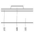
도 1은 본 발명의 일 실시예에 의한 박막 트랜지스터 표시판의 한 화소를 나타낸 배치도이다.
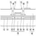
도 2는 도 1의 II-II선을 따라 나타낸 본 발명의 일 실시예에 의한 박막 트랜지스터의 단면도이다.
도 3a 내지 도 3n은 본 발명의 일 실시예에 의한 박막 트랜지스터 표시판의 제조 방법을 나타낸 공정 단면도이다.1 is a layout diagram showing one pixel of a thin film transistor panel according to an embodiment of the present invention.
2 is a cross-sectional view of a thin film transistor according to an embodiment of the present invention taken along the line II-II of FIG.
3A to 3N are cross-sectional views illustrating a method of manufacturing a thin film transistor panel according to an exemplary embodiment of the present invention.
이하에서 첨부한 도면을 참고로 하여 본 발명의 실시예에 대하여 본 발명이 속하는 기술 분야에서 통상의 지식을 가진 자가 용이하게 실시할 수 있도록 상세히 설명한다. 그러나 본 발명은 여러 가지 상이한 형태로 구현될 수 있으며 여기에서 설명하는 실시예에 한정되지 않는다.Hereinafter, exemplary embodiments of the present invention will be described in detail with reference to the accompanying drawings, which will be readily apparent to those skilled in the art to which the present invention pertains. The present invention may, however, be embodied in many different forms and should not be construed as limited to the embodiments set forth herein.
도면에서 여러 층 및 영역을 명확하게 표현하기 위하여 두께를 확대하여 나타내었다. 명세서 전체를 통하여 유사한 부분에 대해서는 동일한 도면 부호를 붙였다. 층, 막, 영역, 판 등의 부분이 다른 부분 "위에" 있다고 할 때, 이는 다른 부분 "바로 위에" 있는 경우뿐 아니라 그 중간에 또 다른 부분이 있는 경우도 포함한다. 반대로 어떤 부분이 다른 부분 "바로 위에" 있다고 할 때에는 중간에 다른 부분이 없는 것을 뜻한다.
In the drawings, the thickness is enlarged to clearly represent the layers and regions. Like parts are designated with like reference numerals throughout the specification. It will be understood that when an element such as a layer, film, region, plate, or the like is referred to as being "on" another portion, it includes not only the element directly over another element, Conversely, when a part is "directly over" another part, it means that there is no other part in the middle.
먼저, 첨부된 도면을 참조하여 본 발명의 일 실시예에 의한 박막 트랜지스터 표시판에 대해 설명하면 다음과 같다.First, a thin film transistor display panel according to an embodiment of the present invention will be described with reference to the accompanying drawings.
도 1은 본 발명의 일 실시예에 의한 박막 트랜지스터 표시판의 한 화소를 나타낸 배치도이고, 도 2는 도 1의 II-II선을 따라 나타낸 본 발명의 일 실시예에 의한 박막 트랜지스터의 단면도이다.FIG. 1 is a layout diagram showing one pixel of a thin film transistor panel according to an embodiment of the present invention, and FIG. 2 is a cross-sectional view of a thin film transistor according to an embodiment of the present invention along a line II-II of FIG.
본 발명의 일 실시예에 의한 박막 트랜지스터 표시판의 기판(110) 위에는 다결정 규소로 이루어진 반도체층(150)이 형성되어 있다. 반도체층(150)은 소스 영역(152), 드레인 영역(154), 및 소스 영역(152)과 드레인 영역(154) 사이에 위치하는 채널 영역(156)을 포함한다.A
반도체층(150)은 소스 영역(152)과 채널 영역(156)의 사이에 저농도로 도핑된 제1 저농도 도핑 영역(157)을 더 포함할 수 있고, 드레인 영역(154)과 채널 영역(156)의 사이에 저농도로 도핑된 제2 저농도 도핑 영역(158)을 더 포함할 수 있다.The
반도체층(150)을 포함한 기판(110) 위의 전면에는 제1 절연막(114)이 형성되어 있다.A first
제1 절연막(114) 위에는 반도체층(150)의 채널 영역(156)과 중첩하여 게이트 전극(124)이 형성되어 있다. 게이트 전극(124)의 좌측 아래에 위치한 반도체층(150)은 소스 영역(152)에 해당하고, 게이트 전극(124)의 우측 아래에 위치한 반도체층(150)은 드레인 영역(154)에 해당한다.A
제1 절연막(114) 위에는 일방향으로 뻗어 있는 게이트선(121)이 형성되어 있고, 게이트 전극(124)은 게이트선(121)으로부터 돌출되어 있다.A
게이트 전극(124)을 포함한 기판(110) 위의 전면에는 제2 절연막(140)이 형성되어 있다. 제2 절연막(140)은 무기 절연 물질로 이루어진 제2 하부 절연막(142) 및 유기 절연 물질로 이루어진 제2 상부 절연막(144)을 포함하는 이중막으로 이루어질 수 있다. 이와 달리 제2 하부 절연막(142)이 유기 절연 물질로 이루어지고, 제2 상부 절연막(144)이 무기 절연 물질로 이루어질 수도 있으며, 제2 절연막(140)은 단일막으로 이루어질 수도 있다.A second
제1 절연막(114) 및 제2 절연막(140)에는 반도체층(150)의 소스 영역(152)의 적어도 일부를 노출하도록 제1 접촉 구멍(146)이 형성되어 있고, 드레인 영역(154)의 적어도 일부를 노출하도록 제2 접촉 구멍(148)이 형성되어 있다.A
제2 절연막(140) 위에는 제1 접촉 구멍(146)의 외곽을 둘러싸도록 소스 전극(173)이 형성되어 있다. 제2 절연막(140) 위에는 게이트선(121)과 교차하도록 데이터선(171)이 형성되어 있고, 소스 전극(173)은 데이터선(171)으로부터 돌출되어 있다. 제2 절연막(140) 위에는 제2 접촉 구멍(148)의 외곽을 둘러싸도록 드레인 전극(175)이 형성되어 있다.A
제1 접촉 구멍(146)의 내부에는 제1 연결 전극(177)이 형성되어 있고, 제1 연결 전극(177)은 제1 접촉 구멍(146)을 통해 반도체층(150)의 소스 영역(152)과 소스 전극(173)을 연결한다. 제1 연결 전극(177)은 소스 전극(173)의 측면을 덮도록 형성되어 있고, 소스 전극(173)의 윗면에는 형성되지 않을 수 있다. 제1 연결 전극(177)은 데이터선(171)의 측면까지 덮도록 연장되어 형성될 수 있다.A
제2 접촉 구멍(148)의 내부에는 제2 연결 전극(179)이 형성되어 있고, 제2 연결 전극(179)은 제2 접촉 구멍(148)을 통해 반도체층(150)의 드레인 영역(154)과 드레인 전극(175)을 연결한다. 제2 연결 전극(179)은 드레인 전극(175)의 측면을 덮도록 형성되어 있고, 드레인 전극(175)의 윗면에는 형성되지 않을 수 있다.A
제1 접촉 구멍(146), 제2 접촉 구멍(148), 소스 전극(173), 드레인 전극(175), 제1 연결 전극(177), 및 제2 연결 전극(179)은 하나의 마스크를 이용하여 형성될 수 있다. 이때 사용되는 마스크는 슬릿 마스크 또는 하프톤(half-tone) 마스크 등일 수 있다. 제1 접촉 구멍(146), 제2 접촉 구멍(148), 소스 전극(173), 드레인 전극(175), 제1 연결 전극(177), 및 제2 연결 전극(179)을 형성하는 자세한 공정에 대해서는 이하 제조 방법에서 설명한다.The
소스 전극(173), 드레인 전극(175)을 포함한 기판(110) 위의 전면에는 제3 절연막(180)이 형성되어 있다.A third insulating
제3 절연막(180)에는 드레인 전극(175)의 적어도 일부를 노출하도록 제3 접촉 구멍(181)이 형성되어 있다.A
제3 절연막(180) 위에는 제3 접촉 구멍(181)을 통해 드레인 전극(175)과 연결되는 화소 전극(191)이 형성되어 있다. 게이트선(121)과 데이터선(171)은 서로 교차되어 화소 영역을 정의할 수 있고, 화소 전극(191)은 화소 영역에 형성될 수 있다.A
기판(110)과 반도체층(150) 사이에는 버퍼층(112)이 더 형성될 수 있다. 반도체층(150)은 기판(110) 바로 위에 형성될 수도 있고, 도 2에 도시된 바와 같이 기판(110) 바로 위에 버퍼층(112)이 형성되고, 버퍼층(112) 위에 반도체층(150)이 형성될 수도 있다. 버퍼층(112)은 반도체층(150)이 기판(110)의 이물질에 의해 영향을 받는 것을 방지하기 위해 형성된다.
A
다음으로, 첨부된 도면을 참조하여 본 발명의 일 실시예에 의한 박막 트랜지스터 표시판의 제조 방법에 대해 설명하면 다음과 같다.Next, a method of manufacturing a thin film transistor panel according to an embodiment of the present invention will be described with reference to the accompanying drawings.
도 3a 내지 도 3n은 본 발명의 일 실시예에 의한 박막 트랜지스터 표시판의 제조 방법을 나타낸 공정 단면도이다.3A to 3N are cross-sectional views illustrating a method of manufacturing a thin film transistor panel according to an exemplary embodiment of the present invention.
먼저, 도 3a에 도시된 바와 같이, 유리 또는 플라스틱 등으로 이루어진 기판(110) 위에 버퍼층(112)을 형성한다.First, as shown in FIG. 3A, a
버퍼층(112) 위에 비정질 규소층을 형성하고, 이를 패터닝한 후 가열 등의 방법으로 결정화하여 반도체층(150)을 형성한다. 이때, 비정질 규소층을 결정화한 후 패터닝하여 반도체층(150)을 형성하는 방법도 가능하다.An amorphous silicon layer is formed on the
버퍼층(112)을 형성하는 공정은 생략될 수 있으며, 버퍼층(112)을 형성하는 경우 반도체층(150)을 형성하는 과정에서 기판(110)의 이물질이 반도체층(150)에 침투하여 이를 손상시키는 것을 억제할 수 있다.The
도 3b에 도시된 바와 같이, 반도체층(150)을 포함하는 기판(110) 위의 전면에 제1 절연막(114)을 형성한다.The first insulating
이어, 제1 절연막 위에 금속 물질을 이용하여 일방향으로 뻗어 있는 게이트선(도시하지 않음) 및 게이트선으로부터 돌출되는 게이트 전극(124)을 형성한다. 게이트 전극(124)은 적어도 일부가 반도체층(150)과 중첩하도록 형성하고, 구체적으로 반도체층의 중앙부와 중첩하도록 형성할 수 있다.Next, a gate line (not shown) extending in one direction and a
이어, 게이트 전극(124)을 마스크로 하여 반도체층(150)에 이온을 도핑하여 소스 영역(152) 및 드레인 영역(154)을 형성한다. 소스 영역(152)은 게이트 전극(124)의 좌측 아래에 위치하고, 드레인 영역(154)은 게이트 전극(124)의 우측 아래에 위치한다. 이에 따라, 소스 영역(152)과 드레인 영역(154) 사이의 게이트 전극(124) 아래에는 채널 영역(156)이 형성된다.Next, the
이때, 채널 영역(156)을 중심으로 양측에 저농도로 도핑된 제1 저농도 도핑 영역(157) 및 제2 저농도 도핑 영역(158)을 더 형성할 수 있다. 제1 저농도 도핑 영역(157)은 소스 영역(152)과 채널 영역(156) 사이에 위치하고, 제2 저농도 도핑 영역(158)은 드레인 영역(154)과 채널 영역(156) 사이에 위치한다.At this time, the first lightly doped
도 3c에 도시된 바와 같이, 게이트 전극(124)을 포함한 기판(110) 전면 위에 제2 절연막(140)을 형성한다.The second
제2 절연막(140)은 제2 하부 절연막(142) 및 제2 상부 절연막(144)으로 이루어질 수 있다. 먼저, 무기 절연 물질을 이용하여 게이트 전극(124)을 포함한 기판(110) 전면에 제2 하부 절연막(142)을 형성하고, 제2 하부 절연막(142) 위에 유기 절연 물질을 이용하여 제2 상부 절연막(144)을 형성할 수 있다.The second
이와 다른 방법으로, 유기 절연 물질을 이용하여 게이트 전극(124)을 포함한 기판(110) 전면에 제2 하부 절연막(142)을 형성하고, 제2 하부 절연막(142) 위에 무기 절연 물질을 이용하여 제2 상부 절연막(144)을 형성할 수도 있다. 또한, 제2 절연막(140)을 단일막으로 형성할 수도 있다.Alternatively, a second lower insulating
도 3d에 도시된 바와 같이, 제2 절연막(140) 위에 금속 물질을 이용하여 제1 금속층(170)을 형성한다.As shown in FIG. 3D, a
이어, 제1 금속층(170) 위에 감광 물질을 도포하고, 마스크를 이용하여 노광 및 현상함으로써 제1 두께(T1) 및 제2 두께(T2)를 가지는 제1 감광막(40)을 형성한다. 이때 사용되는 마스크는 슬릿 마스크 또는 하프톤(half-tone) 마스크 등일 수 있다. 예를 들면, 마스크에 패턴이 형성되지 않은 부분에 대응하는 감광 물질은 제거되고, 마스크에 패턴이 형성된 부분에 대응하여 제1 두께(T1)를 가지는 제1 감광막(40)이 형성되며, 마스크에 슬릿 패턴이 형성된 부분에 대응하여 제2 두께(T2)를 가지는 제1 감광막(40)이 형성될 수 있다.Next, a photosensitive material is coated on the
도 3e에 도시된 바와 같이, 제1 감광막(40)을 마스크로 하여 제1 금속층(170)의 일부를 제거한다. 제1 감광막(40)을 마스크로 하여 제1 금속층(170)을 식각하면, 제1 감광막(40)이 형성되지 않은 부분에 대응하는 제1 금속층(170)은 제거된다.3E, a portion of the
이때, 제1 금속층(170)이 제거되는 부분은 반도체층(150)의 소스 영역(152) 및 드레인 영역(154) 위에 위치하는 부분이다.At this time, the portion where the
도 3f에 도시된 바와 같이, 제1 감광막(40)을 애싱하여 제2 두께(T2)를 가지는 제1 감광막(40)을 제거한다.As shown in FIG. 3F, the
이어, 애싱된 제1 감광막(40)을 마스크로 하여 제1 금속층(170)의 일부의 두께를 감소시킨다. 애싱된 제1 감광막(40)을 마스크로 하여 제1 금속층(170)을 식각하면, 제1 감광막(40)이 제거된 부분에 대응하는 제1 금속층(170)의 두께가 감소한다. 이때, 제1 감광막(40)이 제거된 부분에 대응하는 제1 금속층(170)이 제거되지 않고, 제4 두께(T4)를 가지고 남아있도록 시간 및 강도를 설정하여 식각한다. 제1 감광막(40)이 남아있는 부분의 아래에 위치하는 제1 금속층(170)은 제3 두께(T3)를 가지며, 제3 두께(T3)는 제4 두께(T4)보다 두껍다.Then, the thickness of a portion of the
도 3g에 도시된 바와 같이, 남아있는 제1 감광막(40)을 제거한다.The remaining
이어, 제1 금속층(170)을 마스크로 하여 제1 절연막(112) 및 제2 절연막(140)을 식각하여 제1 접촉 구멍(146) 및 제2 접촉 구멍(148)을 형성한다. 제1 접촉 구멍(146)은 반도체층(150)의 소스 영역(152)의 적어도 일부를 노출하도록 형성하고, 제2 접촉 구멍(148)은 반도체층(150)의 드레인 영역(154)의 적어도 일부를 노출하도록 형성한다.The
제1 접촉 구멍(146) 및 제2 접촉 구멍(148)을 형성하는 공정에서 제1 금속층(170)을 마스크로 이용함으로써, 금속이 아닌 감광막을 마스크로 이용할 때보다 높은 선택성을 가지고 식각할 수 있다. 이에 따라 제1 감광막(40)은 상대적으로 얇게 형성해도 무방하다.By using the
상기에서 설명한 바와 달리 제1 접촉 구멍(146) 및 제2 접촉 구멍(148)을 먼저 형성한 후 제1 감광막(40)을 제거하는 방법도 가능하다.The
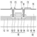
도 3h에 도시된 바와 같이, 제1 금속층(170)을 전면 식각한다. 이때, 두께가 감소된 제1 금속층(170)을 제거할 수 있는 조건으로 식각한다. 즉, 제4 두께(T4)를 가지는 제1 금속층(170)을 제거할 수 있을 정도의 시간 및 강도로 식각을 진행하여 제1 금속층(170)의 전체의 두께를 감소시킨다. 이에 따라 제3 두께(T3)를 가지는 제1 금속층(170)은 제3 두께(T3)보다 더 얇은 두께를 가지게 된다.As shown in Figure 3h, the
남아있는 제1 금속층(170)은 데이터선(도시하지 않음), 소스 전극(173), 및 드레인 전극(175)을 이룬다. 즉, 제1 금속층(170)을 전면 식각함으로써, 게이트선과 교차하도록 데이터선을 형성한다. 또한, 데이터선으로부터 돌출되어 제1 접촉 구멍(146)의 외곽을 둘러싸도록 제2 절연막(140) 위에 소스 전극(173)을 형성하고, 제2 접촉 구멍(148)의 외곽을 둘러싸도록 제2 절연막(140) 위에 드레인 전극(175)을 형성한다.The remaining
제1 금속층(170)을 식각하는 단계에서 제1 접촉 구멍(146) 및 제2 접촉 구멍(148)에 의해 노출된 반도체층(150)의 소스 영역(152) 및 드레인 영역(154)이 손상될 수 있다. 이때, 약 350도의 온도로 약 30분 정도 어닐링 공정을 진행함으로써, 손상된 반도체층(150)의 소스 영역(152) 및 드레인 영역(154)을 복구할 수 있다.The
도 3i에 도시된 바와 같이, 소스 전극(173) 및 드레인 전극(175)을 포함한 기판(110) 전면 위에 금속 물질을 이용하여 제2 금속층(176)을 형성한다. 이때, 제2 금속층(176)은 제1 접촉 구멍(146) 및 제2 접촉 구멍(148)의 내에도 형성된다.A
도 3j에 도시된 바와 같이, 제2 금속층(176) 위에 제2 감광막(50)을 형성한다. 제2 감광막(50)은 기판(110) 위의 전 영역에 걸쳐 평탄하게 형성될 수 있을 정도의 충분한 두께를 가지도록 형성한다.The
도 3k에 도시된 바와 같이, 제2 감광막(50)을 애싱하여 제1 접촉 구멍(146) 및 제2 접촉 구멍(148)을 메우는 부분에 위치한 제2 감광막(50)만을 남기고 나머지 부분에 위치한 제2 감광막(50)은 제거한다.3K, the
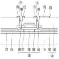
도 3l에 도시된 바와 같이, 남아있는 제2 감광막(50)을 마스크로 하여 제2 금속층(176)을 전면 식각한다. 이때, 제2 절연막(140)의 바로 위에 형성된 제2 금속층(176)을 제거할 수 있는 조건으로 식각한다. 이에 따라 소스 전극(173) 및 드레인 전극(175)의 바로 위에 위치한 제2 금속층(176)도 제거된다.As shown in FIG. 31, the
남아있는 제2 금속층(176)은 제1 연결 전극(177) 및 제2 연결 전극(179)을 이룬다. 즉, 제2 금속층(176)을 전면 식각함으로써, 제1 접촉 구멍(146)을 통해 반도체층(150)의 소스 영역(152)과 소스 전극(173)을 연결하는 제1 연결 전극(177)을 형성하고, 제2 접촉 구멍(148)을 통해 반도체층(150)의 드레인 영역(154)과 드레인 전극(175)을 연결하는 제2 연결 전극(179)을 형성한다.The remaining
제2 금속층(176)의 식각은 건식 식각으로 이루어지고, 이때 건식 식각은 비등방성을 가지므로 기판(110)과 수평한 방향으로 위치하는 제2 금속층(176)은 제거되고, 기판(110)과 약 70도 이상의 각을 가지는 제2 금속층(176)은 제거되지 않는다. 따라서, 제1 연결 전극(177)은 소스 전극(173)의 측면을 덮도록 형성하고, 제2 연결 전극(179)은 드레인 전극(175)의 측면을 덮도록 형성할 수 있다.The
도시는 생략하였으나, 제1 연결 전극(177)은 데이터선의 측면을 덮도록 연장하여 형성할 수 있다.Although not shown, the first connecting
도 3m에 도시된 바와 같이, 남아 있는 제2 감광막(50)을 모두 제거한다. 이때, 제2 금속층(176)을 식각하는 공정이 끝난 직후에 산소 가스를 공급하여 제2 감광막(50)을 애싱한 후 제2 감광막(50)을 제거하면 제1 접촉 구멍(146) 및 제2 접촉 구멍(148)의 내에 남아 있는 제2 감광막(50)을 완전히 제거할 수 있다.The remaining
도 3n에 도시된 바와 같이, 소스 전극(173) 및 드레인 전극(175) 위에 제3 절연막(180)을 형성한다.A third insulating
이어, 제3 절연막(180)을 패터닝하여 드레인 전극(175)의 적어도 일부를 노출하도록 제3 접촉 구멍(181)을 형성한다.Next, the third
이어, 제3 접촉 구멍(181)을 통해 드레인 전극(175)과 연결되는 화소 전극(191)을 형성한다.
Next, the
이상에서 본 발명의 바람직한 실시예에 대하여 상세하게 설명하였지만 본 발명의 권리범위는 이에 한정되는 것은 아니고 다음의 청구범위에서 정의하고 있는 본 발명의 기본 개념을 이용한 당업자의 여러 변형 및 개량 형태 또한 본 발명의 권리범위에 속하는 것이다.While the present invention has been particularly shown and described with reference to exemplary embodiments thereof, it is to be understood that the invention is not limited to the disclosed exemplary embodiments, Of the right.
40: 제1 감광막50: 제2 감광막
110: 기판112: 버퍼층
114: 제1 절연막121: 게이트선
124: 게이트 전극140: 제2 절연막
142: 제2 하부 절연막144: 제2 상부 절연막
146: 제1 접촉 구멍148: 제2 접촉 구멍
150: 반도체층152: 소스 영역
154: 드레인 영역156: 채널 영역
157: 제1 저농도 도핑 영역158: 제2 저농도 도핑 영역
170: 제1 금속층171: 데이터선
173: 소스 전극175: 드레인 전극
176: 제2 금속층177: 제1 연결 전극
179: 제2 연결 전극180: 제3 절연막
181: 제3 접촉 구멍191: 화소 전극40: first photosensitive film 50: second photosensitive film
110: substrate 112: buffer layer
114: first insulating film 121: gate line
124: gate electrode 140: second insulating film
142: second lower insulating film 144: second upper insulating film
146: first contact hole 148: second contact hole
150: semiconductor layer 152: source region
154: drain region 156: channel region
157: first lightly doped region 158: second lightly doped region
170: first metal layer 171: data line
173: source electrode 175: drain electrode
176: second metal layer 177: first connecting electrode
179: second connection electrode 180: third insulating film
181: third contact hole 191: pixel electrode
Claims (20)
Translated fromKorean상기 기판 위에 형성되고, 다결정 규소로 이루어지며, 소스 영역, 드레인 영역, 및 상기 소스 영역 및 상기 드레인 영역 사이에 위치하는 채널 영역을 포함하는 반도체층;
상기 반도체층 위에 형성되는 제1 절연막;
상기 제1 절연막 위에 상기 반도체층의 채널 영역과 중첩하여 형성되는 게이트 전극;
상기 게이트 전극 위에 형성되는 제2 절연막;
상기 반도체층의 소스 영역 및 상기 반도체층의 드레인 영역의 적어도 일부를 노출하도록 상기 제1 절연막 및 제2 절연막에 형성되는 제1 접촉 구멍 및 제2 접촉 구멍;
상기 제1 접촉 구멍의 외곽을 둘러싸도록 상기 제2 절연막 위에 형성되는 소스 전극;
상기 제2 접촉 구멍의 외곽을 둘러싸도록 상기 제2 절연막 위에 형성되는 드레인 전극;
상기 제1 접촉 구멍을 통해 상기 반도체층의 소스 영역과 상기 소스 전극을 연결하는 제1 연결 전극; 및,
상기 제2 접촉 구멍을 통해 상기 반도체층의 드레인 영역과 상기 드레인 전극을 연결하는 제2 연결 전극을 포함하며,
상기 제1 접촉 구멍, 상기 제2 접촉 구멍, 상기 소스 전극, 상기 드레인 전극, 상기 제1 연결 전극, 및 상기 제2 연결 전극은 하나의 마스크를 이용하여 형성되는,
박막 트랜지스터 표시판.Board;
A semiconductor layer formed on the substrate, the semiconductor layer comprising a polycrystalline silicon and including a source region, a drain region, and a channel region located between the source region and the drain region;
A first insulating layer formed on the semiconductor layer;
A gate electrode formed on the first insulating film so as to overlap the channel region of the semiconductor layer;
A second insulating layer formed on the gate electrode;
A first contact hole and a second contact hole formed in the first insulating film and the second insulating film to expose at least a part of the source region of the semiconductor layer and the drain region of the semiconductor layer;
A source electrode formed on the second insulating film so as to surround an outer periphery of the first contact hole;
A drain electrode formed on the second insulating film so as to surround an outer periphery of the second contact hole;
A first connection electrode connecting the source region of the semiconductor layer and the source electrode through the first contact hole; And
And a second connection electrode connecting the drain region of the semiconductor layer and the drain electrode through the second contact hole,
Wherein the first contact hole, the second contact hole, the source electrode, the drain electrode, the first connection electrode, and the second connection electrode are formed using one mask,
Thin film transistor display panel.
상기 제1 연결 전극은 상기 소스 전극의 측면을 덮도록 형성되고,
상기 제2 연결 전극은 상기 드레인 전극의 측면을 덮도록 형성되는,
박막 트랜지스터 표시판.The method according to claim 1,
Wherein the first connection electrode is formed to cover a side surface of the source electrode,
And the second connection electrode is formed to cover the side surface of the drain electrode,
Thin film transistor display panel.
상기 게이트 전극과 연결되는 게이트선; 및
상기 소스 전극과 연결되는 데이터선을 더 포함하는,
박막 트랜지스터 표시판.The method according to claim 1,
A gate line connected to the gate electrode; And
And a data line connected to the source electrode,
Thin film transistor display panel.
상기 제1 연결 전극은 상기 데이터선의 측면을 덮도록 연장되어 형성되는,
박막 트랜지스터 표시판.5. The method of claim 4,
Wherein the first connection electrode extends to cover a side surface of the data line,
Thin film transistor display panel.
상기 소스 전극 및 상기 드레인 전극 위에 형성되는 제3 절연막;
상기 드레인 전극의 적어도 일부를 노출하도록 상기 제3 절연막에 형성되는 제3 접촉 구멍; 및,
상기 제3 접촉 구멍을 통해 상기 드레인 전극과 연결되는 화소 전극을 더 포함하는,
박막 트랜지스터 표시판.The method according to claim 1,
A third insulating layer formed on the source electrode and the drain electrode;
A third contact hole formed in the third insulating film to expose at least a part of the drain electrode; And
And a pixel electrode connected to the drain electrode through the third contact hole.
Thin film transistor display panel.
상기 기판과 상기 반도체층 사이에 형성되는 버퍼층을 더 포함하고,
상기 제2 절연막은 무기 절연 물질 및 유기 절연 물질을 포함하는 이중막으로 이루어진,
박막 트랜지스터 표시판.The method according to claim 1,
And a buffer layer formed between the substrate and the semiconductor layer,
Wherein the second insulating film is made of a double film including an inorganic insulating material and an organic insulating material,
Thin film transistor display panel.
(b) 상기 반도체층 위에 제1 절연막을 형성하는 단계;
(c) 상기 제1 절연막 위에 상기 반도체층과 일부분이 중첩하는 게이트 전극을 형성하는 단계;
(d) 상기 반도체층에 불순물을 도핑하여 소스 영역 및 드레인 영역을 형성하는 단계;
(e) 상기 게이트 전극 위에 제2 절연막을 형성하는 단계;
(f) 상기 제2 절연막 위에 제1 금속층을 형성하는 단계;
(g) 상기 제1 금속층 위에 제1 두께 및 제2 두께를 가지는 제1 감광막을 형성하는 단계;
(h) 상기 제1 감광막을 마스크로 사용하여 상기 반도체층의 소스 영역 및 드레인 영역 위에 위치하는 상기 제1 금속층의 일부를 제거하는 단계;
(i) 상기 제1 감광막을 애싱하여 상기 제2 두께를 가지는 상기 제1 감광막을 제거하는 단계;
(j) 제거된 상기 제1 감광막의 아래에 위치하는 상기 제1 금속층의 두께를 감소시키는 단계;
(k) 상기 제1 절연막 및 상기 제2 절연막을 패터닝하여 상기 반도체층의 소스 영역 및 드레인 영역의 적어도 일부를 노출하는 제1 접촉 구멍 및 제2 접촉 구멍을 형성하는 단계;
(l) 상기 제1 금속층을 전면 식각하는 단계;
(m) 상기 제1 금속층을 포함한 상기 기판 전면에 제2 금속층을 형성하는 단계;
(n) 상기 제2 금속층 위에 상기 제1 접촉 구멍 및 상기 제2 접촉 구멍을 메우도록 제2 감광막을 형성하는 단계; 및,
(o) 상기 제2 금속층을 전면 식각하는 단계를 포함하는,
박막 트랜지스터 표시판의 제조 방법.(a) forming a semiconductor layer of polycrystalline silicon on a substrate;
(b) forming a first insulating layer on the semiconductor layer;
(c) forming a gate electrode on the first insulating film, the gate electrode overlapping with the semiconductor layer;
(d) doping the semiconductor layer with an impurity to form a source region and a drain region;
(e) forming a second insulating film on the gate electrode;
(f) forming a first metal layer on the second insulating layer;
(g) forming a first photoresist layer having a first thickness and a second thickness on the first metal layer;
(h) removing a portion of the first metal layer located on the source region and the drain region of the semiconductor layer using the first photoresist layer as a mask;
(i) ashing the first photoresist layer to remove the first photoresist layer having the second thickness;
(j) reducing a thickness of the first metal layer located under the removed first photoresist layer;
(k) forming a first contact hole and a second contact hole exposing at least a part of a source region and a drain region of the semiconductor layer by patterning the first insulating film and the second insulating film;
(l) etching the first metal layer;
(m) forming a second metal layer on the entire surface of the substrate including the first metal layer;
(n) forming a second photoresist film on the second metal layer to fill the first contact hole and the second contact hole; And
(o) front-etching the second metal layer.
A method of manufacturing a thin film transistor display panel.
상기 (l) 단계에서,
두께가 감소된 상기 제1 금속층을 제거할 수 있는 조건으로 식각하여, 상기 제1 접촉 구멍의 외곽을 둘러싸도록 상기 제2 절연막 위에 소스 전극을 형성하고, 상기 제2 접촉 구멍의 외곽을 둘러싸도록 상기 제2 절연막 위에 드레인 전극을 형성하는,
박막 트랜지스터 표시판의 제조 방법.9. The method of claim 8,
In the step (l)
Forming a source electrode on the second insulating film so as to surround an outer periphery of the first contact hole by etching the first metal layer having a reduced thickness so as to remove the first metal layer, Forming a drain electrode on the second insulating film,
A method of manufacturing a thin film transistor display panel.
상기 (o) 단계에서,
상기 제2 절연막의 바로 위에 형성된 상기 제2 금속층을 제거할 수 있는 조건으로 식각하여, 상기 제1 접촉 구멍을 통해 상기 반도체층의 소스 영역과 상기 소스 전극을 연결하는 제1 연결 전극을 형성하고, 상기 제2 접촉 구멍을 통해 상기 반도체층의 드레인 영역과 상기 드레인 전극을 연결하는 제2 연결 전극을 형성하는,
박막 트랜지스터 표시판의 제조 방법.10. The method of claim 9,
In the step (o)
Forming a first connection electrode that connects the source region of the semiconductor layer and the source electrode through the first contact hole by etching the second metal layer formed immediately above the second insulation layer, And forming a second connection electrode connecting the drain region of the semiconductor layer and the drain electrode through the second contact hole,
A method of manufacturing a thin film transistor display panel.
상기 (o) 단계에서,
상기 제1 연결 전극은 상기 소스 전극의 측면을 덮도록 형성하고,
상기 제2 연결 전극은 상기 드레인 전극의 측면을 덮도록 형성하는,
박막 트랜지스터 표시판의 제조 방법.11. The method of claim 10,
In the step (o)
The first connection electrode is formed to cover the side surface of the source electrode,
And the second connection electrode is formed to cover the side surface of the drain electrode,
A method of manufacturing a thin film transistor display panel.
상기 (g) 단계 내지 상기 (o) 단계는 하나의 마스크를 이용하여 이루어지는,
박막 트랜지스터 표시판의 제조 방법.12. The method of claim 11,
Wherein the steps (g) to (o) are performed using one mask,
A method of manufacturing a thin film transistor display panel.
상기 (o) 단계 이후에,
(p) 산소 가스를 공급하여 상기 제2 감광막을 애싱한 후, 상기 제2 감광막을 제거하는 단계를 더 포함하는,
박막 트랜지스터 표시판의 제조 방법.12. The method of claim 11,
After the step (o)
(p) after the second photoresist film is ashed by supplying oxygen gas, removing the second photoresist film.
A method of manufacturing a thin film transistor display panel.
상기 (l) 단계에서,
상기 제1 금속층을 전면 식각한 후, 어닐링하는,
박막 트랜지스터 표시판의 제조 방법.12. The method of claim 11,
In the step (l)
Wherein the first metal layer is front-etched and then annealed,
A method of manufacturing a thin film transistor display panel.
상기 (n) 단계는,
(n-1) 상기 제2 금속층 위에 상기 제2 감광막을 도포하는 단계; 및,
(n-2) 상기 제2 감광막을 애싱하여 상기 제1 접촉 구멍 및 상기 제2 접촉 구멍 내에 위치한 상기 제2 감광막을 남기는 단계를 포함하는,
박막 트랜지스터 표시판의 제조 방법.12. The method of claim 11,
The step (n)
(n-1) applying the second photoresist over the second metal layer; And
and (n-2) ashing the second photosensitive film to leave the first contact hole and the second photosensitive film positioned in the second contact hole.
A method of manufacturing a thin film transistor display panel.
상기 (c) 단계에서, 상기 게이트 전극과 연결되는 게이트선을 더 형성하고,
상기 (l) 단계에서, 상기 소스 전극과 연결되는 데이터선을 더 형성하는,
박막 트랜지스터 표시판의 제조 방법.12. The method of claim 11,
In the step (c), a gate line connected to the gate electrode is further formed,
In the step (l), a data line connected to the source electrode is further formed.
A method of manufacturing a thin film transistor display panel.
상기 (o) 단계에서,
상기 제1 연결 전극이 상기 데이터선의 측면을 덮도록 연장하여 형성하는,
박막 트랜지스터 표시판의 제조 방법.17. The method of claim 16,
In the step (o)
The first connection electrode extends to cover a side surface of the data line,
A method of manufacturing a thin film transistor display panel.
상기 (o) 단계 이후에,
(q) 상기 소스 전극 및 상기 드레인 전극 위에 제3 절연막을 형성하는 단계;
(r) 상기 제3 절연막을 패터닝하여 상기 드레인 전극의 적어도 일부를 노출하도록 제3 접촉 구멍을 형성하는 단계; 및,
(s) 상기 제3 접촉 구멍을 통해 상기 드레인 전극과 연결되는 화소 전극을 형성하는 단계를 더 포함하는,
박막 트랜지스터 표시판의 제조 방법.12. The method of claim 11,
After the step (o)
(q) forming a third insulating film on the source electrode and the drain electrode;
(r) patterning the third insulating film to form a third contact hole so as to expose at least a part of the drain electrode; And
(s) forming a pixel electrode connected to the drain electrode through the third contact hole.
A method of manufacturing a thin film transistor display panel.
상기 (a) 단계에서,
상기 반도체층을 형성하기 전에, 상기 기판 위에 버퍼층을 형성하는,
박막 트랜지스터 표시판의 제조 방법.12. The method of claim 11,
In the step (a)
Forming a buffer layer on the substrate before forming the semiconductor layer;
A method of manufacturing a thin film transistor display panel.
상기 (e) 단계에서,
상기 제2 절연막은 무기 절연 물질 및 유기 절연 물질을 포함하는 이중막으로 형성하는,
박막 트랜지스터 표시판의 제조 방법.
12. The method of claim 11,
In the step (e)
Wherein the second insulating film is formed of a double film including an inorganic insulating material and an organic insulating material,
A method of manufacturing a thin film transistor display panel.
Priority Applications (3)
| Application Number | Priority Date | Filing Date | Title |
|---|---|---|---|
| KR1020110102550AKR101903671B1 (en) | 2011-10-07 | 2011-10-07 | Thin film transistor array panel and manufacturing method thereof |
| US13/424,278US8653530B2 (en) | 2011-10-07 | 2012-03-19 | Thin film transistor array panel |
| US14/151,658US9041001B2 (en) | 2011-10-07 | 2014-01-09 | Thin film transistor array panel and manufacturing method thereof |
Applications Claiming Priority (1)
| Application Number | Priority Date | Filing Date | Title |
|---|---|---|---|
| KR1020110102550AKR101903671B1 (en) | 2011-10-07 | 2011-10-07 | Thin film transistor array panel and manufacturing method thereof |
Publications (2)
| Publication Number | Publication Date |
|---|---|
| KR20130037963A KR20130037963A (en) | 2013-04-17 |
| KR101903671B1true KR101903671B1 (en) | 2018-10-04 |
Family
ID=48041509
Family Applications (1)
| Application Number | Title | Priority Date | Filing Date |
|---|---|---|---|
| KR1020110102550AActiveKR101903671B1 (en) | 2011-10-07 | 2011-10-07 | Thin film transistor array panel and manufacturing method thereof |
Country Status (2)
| Country | Link |
|---|---|
| US (2) | US8653530B2 (en) |
| KR (1) | KR101903671B1 (en) |
Families Citing this family (3)
| Publication number | Priority date | Publication date | Assignee | Title |
|---|---|---|---|---|
| KR101903671B1 (en)* | 2011-10-07 | 2018-10-04 | 삼성디스플레이 주식회사 | Thin film transistor array panel and manufacturing method thereof |
| KR20130117558A (en)* | 2012-04-18 | 2013-10-28 | 삼성디스플레이 주식회사 | Thin film transistor, thin film transistor array panel and manufacturing method for a thin film transistor array panel |
| KR102567715B1 (en)* | 2016-04-29 | 2023-08-17 | 삼성디스플레이 주식회사 | Transistor array panel and manufacturing method thereof |
Citations (2)
| Publication number | Priority date | Publication date | Assignee | Title |
|---|---|---|---|---|
| JP2005115362A (en)* | 2003-09-19 | 2005-04-28 | Semiconductor Energy Lab Co Ltd | Display device and method for manufacturing display device |
| US20070263133A1 (en) | 1997-03-26 | 2007-11-15 | Semiconductor Energy Laboratory Co., Ltd. | Display device |
Family Cites Families (23)
| Publication number | Priority date | Publication date | Assignee | Title |
|---|---|---|---|---|
| KR100333153B1 (en)* | 1993-09-07 | 2002-12-05 | 가부시키가이샤 한도오따이 에네루기 켄큐쇼 | Process for fabricating semiconductor device |
| JPH09265114A (en) | 1996-03-28 | 1997-10-07 | Canon Inc | Liquid crystal display |
| JP3126661B2 (en)* | 1996-06-25 | 2001-01-22 | 株式会社半導体エネルギー研究所 | Liquid crystal display |
| TW451447B (en)* | 1999-12-31 | 2001-08-21 | Samsung Electronics Co Ltd | Contact structures of wirings and methods for manufacturing the same, and thin film transistor array panels including the same and methods for manufacturing the same |
| US6771328B2 (en)* | 2001-07-25 | 2004-08-03 | Lg. Philips Lcd Co., Ltd. | Active matrix organic electroluminescent device simplifying a fabricating process and a fabricating method thereof |
| KR100796795B1 (en)* | 2001-10-22 | 2008-01-22 | 삼성전자주식회사 | A contact portion of a semiconductor device, a method of manufacturing the same, and a thin film transistor array substrate for a display device including the same, and a method of manufacturing the same |
| KR100412619B1 (en)* | 2001-12-27 | 2003-12-31 | 엘지.필립스 엘시디 주식회사 | Method for Manufacturing of Array Panel for Liquid Crystal Display Device |
| KR100491820B1 (en) | 2002-06-04 | 2005-05-27 | 엘지.필립스 엘시디 주식회사 | array substrate for a low temperature poly silicon liquid crystal display and fabrication method of the same |
| JP4021392B2 (en) | 2002-10-31 | 2007-12-12 | セイコーエプソン株式会社 | Electro-optical device and electronic apparatus |
| JP3622757B2 (en) | 2003-09-10 | 2005-02-23 | セイコーエプソン株式会社 | Liquid crystal display |
| US7520790B2 (en)* | 2003-09-19 | 2009-04-21 | Semiconductor Energy Laboratory Co., Ltd. | Display device and manufacturing method of display device |
| KR101003669B1 (en) | 2003-12-22 | 2010-12-24 | 엘지디스플레이 주식회사 | Reflective type liquid crystal display device and manufacturing method |
| KR101039022B1 (en)* | 2004-02-11 | 2011-06-03 | 삼성전자주식회사 | Contact portion and manufacturing method thereof, thin film transistor array panel and manufacturing method thereof |
| KR100616708B1 (en) | 2004-04-12 | 2006-08-28 | 엘지.필립스 엘시디 주식회사 | LCD array substrate and manufacturing method thereof |
| WO2006022259A1 (en)* | 2004-08-24 | 2006-03-02 | Sharp Kabushiki Kaisha | Active matrix substrate and display unit provided with it |
| KR20060124850A (en) | 2005-05-26 | 2006-12-06 | 엘지.필립스 엘시디 주식회사 | Reflective type liquid crystal display device and manufacturing method thereof |
| KR20060135429A (en) | 2005-06-25 | 2006-12-29 | 엘지.필립스 엘시디 주식회사 | LCD and its manufacturing method |
| US8035103B2 (en)* | 2005-08-11 | 2011-10-11 | Sharp Kabushiki Kaisha | Circuit board, electronic device, and method for producing circuit board |
| JP2007333808A (en) | 2006-06-12 | 2007-12-27 | Mitsubishi Electric Corp | Active matrix display device |
| JP4967631B2 (en)* | 2006-12-07 | 2012-07-04 | 三菱電機株式会社 | Display device |
| KR101224049B1 (en) | 2006-12-14 | 2013-01-18 | 엘지디스플레이 주식회사 | Method of fabricating liquid crystal display device |
| KR100922802B1 (en) | 2006-12-29 | 2009-10-21 | 엘지디스플레이 주식회사 | TFT array substrate and manufacturing method thereof |
| KR101903671B1 (en)* | 2011-10-07 | 2018-10-04 | 삼성디스플레이 주식회사 | Thin film transistor array panel and manufacturing method thereof |
- 2011
- 2011-10-07KRKR1020110102550Apatent/KR101903671B1/enactiveActive
- 2012
- 2012-03-19USUS13/424,278patent/US8653530B2/ennot_activeExpired - Fee Related
- 2014
- 2014-01-09USUS14/151,658patent/US9041001B2/ennot_activeExpired - Fee Related
Patent Citations (2)
| Publication number | Priority date | Publication date | Assignee | Title |
|---|---|---|---|---|
| US20070263133A1 (en) | 1997-03-26 | 2007-11-15 | Semiconductor Energy Laboratory Co., Ltd. | Display device |
| JP2005115362A (en)* | 2003-09-19 | 2005-04-28 | Semiconductor Energy Lab Co Ltd | Display device and method for manufacturing display device |
Also Published As
| Publication number | Publication date |
|---|---|
| US9041001B2 (en) | 2015-05-26 |
| US8653530B2 (en) | 2014-02-18 |
| US20130087800A1 (en) | 2013-04-11 |
| US20140124786A1 (en) | 2014-05-08 |
| KR20130037963A (en) | 2013-04-17 |
Similar Documents
| Publication | Publication Date | Title |
|---|---|---|
| EP2565916B1 (en) | Manufacturing method for array substrate with fringe field switching type thin film transistor liquid crystal display | |
| EP3054483B1 (en) | Array substrate, manufacturing method therefor, and display apparatus | |
| WO2017054384A1 (en) | Array substrate, manufacturing method therefor and display panel | |
| US8278158B2 (en) | Thin film transistor substrate, method of manufacturing the same, and display apparatus having the same | |
| WO2016170571A1 (en) | Thin film transistor production method, thin film transistor and display panel | |
| JP5917015B2 (en) | Method for manufacturing thin film transistor array panel | |
| WO2014124568A1 (en) | Thin film transistor, array substrate, manufacturing method thereof, and display device | |
| JP2008227368A (en) | Thin film transistor, display device using the same, and manufacturing method thereof | |
| WO2015096374A1 (en) | Array substrate and manufacturing method therefor, display device, and thin-film transistor | |
| KR101903671B1 (en) | Thin film transistor array panel and manufacturing method thereof | |
| KR100919636B1 (en) | Patterning method by lift-off and method of fabricating the array substrate for liquid crystal display device of the same | |
| KR101909704B1 (en) | Display substrate and method of manufacturing the display substrate | |
| KR20110125399A (en) | Manufacturing method of thin film transistor and manufacturing method of flat panel display device using same | |
| KR101649732B1 (en) | Thin film transistor array panel and manufacturing method thereof | |
| JP5405770B2 (en) | Display device and manufacturing method thereof | |
| JP2009054836A (en) | TFT substrate and manufacturing method thereof | |
| TWI594440B (en) | Thin film transistor, method for manufacturing thin film transistor, and method for manufacturing array substrate | |
| KR101268388B1 (en) | Fabrication method of liquid crystal display device | |
| KR102140087B1 (en) | Array substrate for fringe field switching mode liquid crystal display device and Method of fabricating thereof | |
| KR20100061977A (en) | Method of fabricating thin film transistor and method of manufacturing display device | |
| JP2009210681A (en) | Display and manufacturing method therefor | |
| JP2007324534A (en) | Thin film transistor substrate and manufacturing method thereof | |
| KR101096721B1 (en) | Method for fabricating of contact wire and method for fabricating liquid crystal display device by using the same | |
| KR19980065262A (en) | LCD and its manufacturing method | |
| KR101193449B1 (en) | Method for fabricating liquid crystal display device using metal gettering method |
Legal Events
| Date | Code | Title | Description |
|---|---|---|---|
| PA0109 | Patent application | Patent event code:PA01091R01D Comment text:Patent Application Patent event date:20111007 | |
| N231 | Notification of change of applicant | ||
| PN2301 | Change of applicant | Patent event date:20120913 Comment text:Notification of Change of Applicant Patent event code:PN23011R01D | |
| PG1501 | Laying open of application | ||
| A201 | Request for examination | ||
| PA0201 | Request for examination | Patent event code:PA02012R01D Patent event date:20161004 Comment text:Request for Examination of Application Patent event code:PA02011R01I Patent event date:20111007 Comment text:Patent Application | |
| E902 | Notification of reason for refusal | ||
| PE0902 | Notice of grounds for rejection | Comment text:Notification of reason for refusal Patent event date:20171212 Patent event code:PE09021S01D | |
| E701 | Decision to grant or registration of patent right | ||
| PE0701 | Decision of registration | Patent event code:PE07011S01D Comment text:Decision to Grant Registration Patent event date:20180621 | |
| GRNT | Written decision to grant | ||
| PR0701 | Registration of establishment | Comment text:Registration of Establishment Patent event date:20180921 Patent event code:PR07011E01D | |
| PR1002 | Payment of registration fee | Payment date:20180921 End annual number:3 Start annual number:1 | |
| PG1601 | Publication of registration | ||
| PR1001 | Payment of annual fee | Payment date:20210825 Start annual number:4 End annual number:4 | |
| PR1001 | Payment of annual fee | Payment date:20220824 Start annual number:5 End annual number:5 | |
| PR1001 | Payment of annual fee | Payment date:20240822 Start annual number:7 End annual number:7 |