KR101902228B1 - Wireless power transmission apparatus and method thereof - Google Patents
Wireless power transmission apparatus and method thereofDownload PDFInfo
- Publication number
- KR101902228B1 KR101902228B1KR1020120121980AKR20120121980AKR101902228B1KR 101902228 B1KR101902228 B1KR 101902228B1KR 1020120121980 AKR1020120121980 AKR 1020120121980AKR 20120121980 AKR20120121980 AKR 20120121980AKR 101902228 B1KR101902228 B1KR 101902228B1
- Authority
- KR
- South Korea
- Prior art keywords
- transistor
- source resonator
- control signal
- power supply
- diode
- Prior art date
- Legal status (The legal status is an assumption and is not a legal conclusion. Google has not performed a legal analysis and makes no representation as to the accuracy of the status listed.)
- Active
Links
Images


Classifications
- H—ELECTRICITY
- H02—GENERATION; CONVERSION OR DISTRIBUTION OF ELECTRIC POWER
- H02J—CIRCUIT ARRANGEMENTS OR SYSTEMS FOR SUPPLYING OR DISTRIBUTING ELECTRIC POWER; SYSTEMS FOR STORING ELECTRIC ENERGY
- H02J50/00—Circuit arrangements or systems for wireless supply or distribution of electric power
- H02J50/10—Circuit arrangements or systems for wireless supply or distribution of electric power using inductive coupling
- H02J50/12—Circuit arrangements or systems for wireless supply or distribution of electric power using inductive coupling of the resonant type
- H—ELECTRICITY
- H02—GENERATION; CONVERSION OR DISTRIBUTION OF ELECTRIC POWER
- H02J—CIRCUIT ARRANGEMENTS OR SYSTEMS FOR SUPPLYING OR DISTRIBUTING ELECTRIC POWER; SYSTEMS FOR STORING ELECTRIC ENERGY
- H02J50/00—Circuit arrangements or systems for wireless supply or distribution of electric power
- H02J50/005—Mechanical details of housing or structure aiming to accommodate the power transfer means, e.g. mechanical integration of coils, antennas or transducers into emitting or receiving devices
- H—ELECTRICITY
- H02—GENERATION; CONVERSION OR DISTRIBUTION OF ELECTRIC POWER
- H02J—CIRCUIT ARRANGEMENTS OR SYSTEMS FOR SUPPLYING OR DISTRIBUTING ELECTRIC POWER; SYSTEMS FOR STORING ELECTRIC ENERGY
- H02J50/00—Circuit arrangements or systems for wireless supply or distribution of electric power
- H02J50/80—Circuit arrangements or systems for wireless supply or distribution of electric power involving the exchange of data, concerning supply or distribution of electric power, between transmitting devices and receiving devices
- H—ELECTRICITY
- H04—ELECTRIC COMMUNICATION TECHNIQUE
- H04B—TRANSMISSION
- H04B5/00—Near-field transmission systems, e.g. inductive or capacitive transmission systems
- H04B5/20—Near-field transmission systems, e.g. inductive or capacitive transmission systems characterised by the transmission technique; characterised by the transmission medium
- H04B5/24—Inductive coupling
- H—ELECTRICITY
- H04—ELECTRIC COMMUNICATION TECHNIQUE
- H04B—TRANSMISSION
- H04B5/00—Near-field transmission systems, e.g. inductive or capacitive transmission systems
- H04B5/70—Near-field transmission systems, e.g. inductive or capacitive transmission systems specially adapted for specific purposes
- H04B5/79—Near-field transmission systems, e.g. inductive or capacitive transmission systems specially adapted for specific purposes for data transfer in combination with power transfer
- H—ELECTRICITY
- H02—GENERATION; CONVERSION OR DISTRIBUTION OF ELECTRIC POWER
- H02J—CIRCUIT ARRANGEMENTS OR SYSTEMS FOR SUPPLYING OR DISTRIBUTING ELECTRIC POWER; SYSTEMS FOR STORING ELECTRIC ENERGY
- H02J7/00—Circuit arrangements for charging or depolarising batteries or for supplying loads from batteries
Landscapes
- Engineering & Computer Science (AREA)
- Computer Networks & Wireless Communication (AREA)
- Power Engineering (AREA)
- Signal Processing (AREA)
- Charge And Discharge Circuits For Batteries Or The Like (AREA)
Abstract
Translated fromKorean
Description
Translated fromKorean아래의 실시 예들은 무선으로 전력을 전송하는 방법 및 장치에 관한 것이다.The following embodiments are directed to a method and apparatus for wirelessly transmitting power.
무선 전력 전송에 대한 연구는 휴대용 단말을 포함한 다양한 전기기기의 폭발적 증가로 인한 유선 전력 공급의 불편 증가 및 기존 배터리(battery) 용량의 한계 등을 극복하기 위해 시작되었다. 그 중에서도 근거리 무선 전력 전송에 대한 연구가 집중되고 있다. 근거리 무선 전력 전송이라 함은 동작 주파수에서 파장의 길이에 비해 송수신 코일간의 거리가 충분히 작은 경우를 의미한다. 공진 특성을 이용하는 무선 전력 송수신 시스템은 전력을 공급하는 소스와 전력을 공급받는 타겟을 포함할 수 있다.Research on wireless power transmission has begun to overcome limitations of existing battery capacity and inconvenience of wired power supply due to explosive increase of various electric devices including portable terminal. Among them, research on near field wireless power transmission is concentrated. Near-field wireless power transmission means that the distance between the transmitting and receiving coils is sufficiently smaller than the wavelength length at the operating frequency. A wireless power transmission / reception system using resonance characteristics may include a power-supplying source and a power-receiving target.
일 측면에 있어서, 무선 전력 전송 장치는 타겟 공진기와의 상호 공진을 통하여 전력을 전송하는 소스 공진기, 상기 소스 공진기로 전력을 공급하는 전원 공급부 및 제어 신호에 기초하여 상기 전원 공급부와 상기 소스 공진기를 연결하는 스위칭부를 포함하고, 상기 스위칭부는 상기 제어 신호의 값과 기준 값을 비교한 결과에 기초하여 상기 전원 공급부와 상기 소스 공진기의 연결을 턴 온(turn on) 또는 턴 오프(turn off)하는 트랜지스터 및 상기 트랜지스터와 직렬로 연결된 다이오드를 포함할 수 있다.In one aspect, a wireless power transmission apparatus includes a source resonator that transmits power through mutual resonance with a target resonator, a power supply unit that supplies power to the source resonator, and a power supply unit that connects the power supply unit and the source resonator Wherein the switching unit turns on or off the connection between the power supply unit and the source resonator based on a result of comparing the value of the control signal with a reference value, And a diode connected in series with the transistor.
다른 일 측면에 있어서, 무선 전력 전송 장치는 상기 제어 신호를 생성하고, 상기 제어 신호의 진폭 및 주기 중 적어도 하나를 제어하는 제어부를 더 포함할 수 있다.In another aspect, the wireless power transmission apparatus may further comprise a control unit for generating the control signal and controlling at least one of the amplitude and the period of the control signal.
상기 턴 온의 상태가 유지되는 동안 상기 다이오드 및 상기 트랜지스터는 상기 전원 공급부로부터 공급하는 직류 전류 신호를 통과시키고, 상기 턴 오프의 상태가 유지되는 동안 상기 다이오드는 상기 소스 공진기에서 발생하는 교류 전류 신호의 플러스 성분의 유입을 차단하고, 상기 트랜지스터는 상기 교류 전류 신호의 마이너스 성분의 유입을 차단할 수 있다.Wherein the diode and the transistor pass a DC current signal supplied from the power supply while the state of the turn-on is maintained, and while the state of the turn-off is maintained, the diode is connected to the AC current signal generated by the source resonator The flow of the positive component is blocked, and the transistor can block the inflow of the negative component of the alternating current signal.
상기 트랜지스터가 피모스(PMOS, P-channel Metal Oxide Semiconductor)인 경우, 상기 제어 신호는 상기 피모스의 게이트에 인가되고, 상기 제어 신호의 전압이 상기 피모스의 소스에 인가되는 전압과 상기 피모스의 문턱전압의 차이보다 작거나 같으면, 상기 전원 공급부와 상기 소스 공진기의 연결을 턴 온(turn on)시키고, 상기 제어 신호의 전압이 상기 피모스의 소스에 인가되는 전압과 상기 피모스의 문턱전압의 차이보다 커지면, 상기 전원 공급부와 상기 소스 공진기의 연결을 턴 오프(turn off)시킬 수 있다.Wherein when the transistor is a PMOS transistor, the control signal is applied to a gate of the PMOS transistor, and a voltage of the control signal is applied to a source of the PMOS transistor, The voltage of the control signal is lower than the voltage applied to the source of the PMOS and the threshold voltage of the PMOS transistor, , The connection between the power supply unit and the source resonator can be turned off.
상기 다이오드는 상기 피모스와 직렬로 연결되고, 상기 다이오드 및 상기 피모스는 상기 턴 온의 상태가 유지되는 동안 상기 전원 공급부로부터 공급하는 직류 전류 신호를 통과시키고, 상기 턴 오프의 상태가 유지되는 동안 상기 소스 공진기로부터 교류 전류 신호의 유입을 차단할 수 있다.The diode is connected in series with the picture element, and the diode and the PMOS pass a DC current signal supplied from the power supply while the state of the turn-on state is maintained, and while the state of the turn- The flow of the alternating current signal from the source resonator can be blocked.
상기 트랜지스터가 엔모스(NMOS, N-channel Metal Oxide Semiconductor)인 경우, 상기 제어 신호는 상기 엔모스의 게이트에 인가되고, 상기 제어 신호의 전압이 상기 엔모스의 소스에 인가되는 전압과 상기 엔모스의 문턱전압의 합보다 크거나 같으면, 상기 전원 공급부와 상기 소스 공진기의 연결을 턴 온(turn on)시키고, 상기 제어 신호의 전압이 상기 엔모스의 소스에 인가되는 전압과 상기 엔모스의 문턱전압의 합보다 작아지면, 상기 전원 공급부와 상기 소스 공진기의 연결을 턴 오프(turn off)시킬 수 있다.Wherein when the transistor is an NMOS transistor, the control signal is applied to a gate of the NMOS transistor, and a voltage of the control signal is applied to a source of the NMOS transistor, Turns on the connection of the power supply and the source resonator and the voltage of the control signal is lower than the voltage applied to the source of the emmos and the threshold voltage of the emmos , The connection between the power supply unit and the source resonator can be turned off.
상기 다이오드는 상기 엔모스와 직렬로 연결되고, 상기 다이오드 및 상기 엔모스는 상기 턴 온의 상태가 유지되는 동안 상기 전원 공급부로부터 공급하는 직류 전류 신호를 통과시키고, 상기 턴 오프의 상태가 유지되는 동안 상기 소스 공진기로부터 교류 전류 신호의 유입을 차단할 수 있다.Wherein the diode is connected in series with the emmos, the diode and the emmos pass a DC current signal supplied from the power supply while the turn-on state is maintained, and while the turn-off state is maintained It is possible to prevent the flow of the AC current signal from the source resonator.
상기 트랜지스터가 바이폴라 접합 트랜지스터(BJT, Bipolar Junction Transistor)인 경우, 상기 트랜지스터는 상기 바이폴라 접합 트랜지스터의 베이스(Base)에 인가되는 상기 제어 신호의 전류 값에 기초하여 상기 전원 공급부와 상기 소스 공진기의 연결을 턴 온(turn on) 또는 턴 오프(turn off)할 수 있다.When the transistor is a bipolar junction transistor (BJT), the transistor is connected to the base of the bipolar junction transistor based on a current value of the control signal, It can be turned on or turned off.
상기 다이오드는 상기 바이폴라 접합 트랜지스터와 직렬로 연결되고, 상기 다이오드 및 상기 바이폴라 접합 트랜지스터는 상기 턴 온의 상태가 유지되는 동안 상기 전원 공급부로부터 공급하는 직류 전류 신호를 통과시키고, 상기 턴 오프의 상태가 유지되는 동안 상기 소스 공진기로부터 교류 전류 신호의 유입을 차단할 수 있다.Wherein the diode is connected in series with the bipolar junction transistor, the diode and the bipolar junction transistor pass a direct current signal supplied from the power supply while the turn-on state is maintained, and the state of the turn- Current signal from the source resonator.
다른 일 측면에 있어서, 무선 전력 전송 장치는 상기 전원 공급부와 상기 스위칭부 사이에 위치하는 가변저항을 더 포함할 수 있다.In another aspect, the wireless power transmission apparatus may further include a variable resistor located between the power supply unit and the switching unit.
다른 일 측면에 있어서, 무선 전력 전송 장치는 상기 전원 공급부와 병렬로 연결되는 복수개의 저항들 및 상기 복수개의 저항들 각각과 직렬로 연결되는 스위치들을 더 포함할 수 있다.In another aspect, the wireless power transmission apparatus may further include a plurality of resistors connected in parallel with the power supply unit, and switches connected in series with each of the plurality of resistors.
상기 제어부는 상기 제어 신호의 진폭을 상기 소스 공진기로 공급할 전력량에 기초하여 제어할 수 있다.The control unit may control the amplitude of the control signal based on an amount of power to be supplied to the source resonator.
상기 제어부는 상기 제어 신호의 주파수를 상기 소스 공진기로 공급할 전력량에 기초하여 제어할 수 있다.The control unit may control the frequency of the control signal based on an amount of power to be supplied to the source resonator.
일 측면에 있어서, 무선 전력 전송 방법은 트랜지스터에 의하여 상기 트랜지스터의 제어 신호의 값과 기준 값을 비교한 결과에 기초하여 전원 공급부와 소스 공진기의 연결을 턴 온(turn on) 또는 턴 오프(turn off)하는 단계, 상기 트랜지스터 및 상기 트랜지스터와 직렬로 연결된 다이오드에 의하여, 상기 트랜지스터의 턴 온 상태에서 상기 전원 공급부의 직류 신호를 통과시키고, 상기 트랜지스터의 턴 오프 상태에서 상기 소스 공진기로부터 교류 신호의 유입을 차단하는 단계, 상기 턴 온 상태에서 상기 전원 공급부로부터 상기 소스 공진기로 전력을 공급하는 단계 및 타겟 공진기와의 상호 공진을 통하여 상기 소스 공진기로부터 전력을 전송하는 단계를 포함할 수 있다.In one aspect, a wireless power transmission method includes turning on or off a connection between a power supply and a source resonator based on a result of comparing a value of a control signal of the transistor with a reference value by a transistor, Passing a direct current signal of the power supply in a turn-on state of the transistor by means of a diode connected in series with the transistor and the transistor, and controlling the flow of the AC signal from the source resonator in the turn- Applying power from the power supply to the source resonator in the turn-on state, and transmitting power from the source resonator through mutual resonance with the target resonator.
다른 일 측면에 있어서, 무선 전력 전송 방법은 상기 제어 신호를 생성하는 단계 및 상기 소스 공진기로 공급하려는 전력량에 기초하여 상기 제어 신호의 진폭 및 주기 중 적어도 하나를 제어하는 단계를 더 포함할 수 있다.In another aspect, a wireless power transmission method may further comprise generating at least one of an amplitude and a period of the control signal based on an amount of power to be supplied to the source resonator, and generating the control signal.
상기 차단하는 단계는 상기 턴 오프의 상태가 유지되는 동안 상기 다이오드에 의하여 상기 소스 공진기에서 발생하는 교류 전류 신호의 플러스 성분의 유입을 차단하고, 상기 트랜지스터에 의하여 상기 교류 전류 신호의 마이너스 성분의 유입을 차단할 수 있다.Wherein the step of interrupting comprises the step of interrupting the inflow of the positive component of the alternating current signal generated in the source resonator by the diode while the state of the turn off is maintained and controlling the inflow of the negative component of the alternating current signal by the transistor Can be blocked.
도 1은 일실시예에 따른 무선 전력 전송 시스템의 등가회로를 나타낸 도면이다.
도 2는 다른 일실시예에 따른 무선 전력 전송 시스템의 등가회로를 나타낸 도면이다.
도 3은 일실시예에 따른 무선 전력 전송 시스템에서 송신단과 수신단의 스위치의 동작 타이밍을 나타낸 도면이다.
도 4는 일실시예에 따른 무선 전력 전송 장치의 블록도이다.
도 5는 다른 일실시예에 따른 무선 전력 전송 장치의 블록도이다.
도 6은 또 다른 일실시예에 따른 무선 전력 전송 장치의 블록도이다.
도 7은 일실시예에 따른 무선 전력 수신 장치의 블록도이다.
도 8은 일실시예에 따른 무선 전력 전송 장치에서, 스위칭부의 동작 및 소스 공진기에 인가되는 전압의 변화를 나타낸다.
도 9는 일실시예에 따른 스위칭 구조를 나타낸 도면이다.
도 10은 일실시예에 따른 무선 전력 전송 장치에 사용되는 스위칭 구조(1010)를 나타낸 도면이다.
도 11은 다른 일실시예에 따른 스위칭 구조를 나타낸 도면이다.
도 12는 일실시예에 따른 무선 전력 수신 장치에 사용되는 스위칭 구조(1210)를 나타낸 도면이다.
도 13은 일실시예에 따른 무선 전력 전송 방법의 흐름도이다.1 is a diagram illustrating an equivalent circuit of a wireless power transmission system according to an embodiment.
2 is a diagram illustrating an equivalent circuit of a wireless power transmission system according to another embodiment.
3 is a diagram illustrating operation timings of switches of a transmitter and a receiver in a wireless power transmission system according to an embodiment.
4 is a block diagram of a wireless power transmission apparatus according to an embodiment.
5 is a block diagram of a wireless power transmission apparatus according to another embodiment.
6 is a block diagram of a wireless power transmission apparatus according to another embodiment.
7 is a block diagram of a wireless power receiving apparatus according to an embodiment.
8 shows the operation of the switching unit and the change in the voltage applied to the source resonator in the wireless power transmission apparatus according to the embodiment.
9 is a diagram illustrating a switching structure according to an embodiment.
10 is a diagram illustrating a
11 is a diagram illustrating a switching structure according to another embodiment.
12 is a diagram illustrating a
13 is a flowchart of a wireless power transmission method according to an embodiment.
이하, 일 측에 따른 실시 예를 첨부된 도면을 참조하여 상세하게 설명한다.Hereinafter, embodiments according to one aspect will be described in detail with reference to the accompanying drawings.
무선 전력 전송 시스템은 무선으로 전력을 필요로 하는 다양한 시스템에 응용될 수 있다. 무선 전력 전송 시스템은 핸드폰 또는 wireless TV 등 무선 전력의 사용이 가능한 시스템에 이용될 수 있다. 또한, 바이오 헬스 케어(bio health care) 분야에 응용이 가능하여, 인체에 삽입된 디바이스에 원격으로 전력을 전송하거나, 심박수 측정을 위한 붕대 모양의 디바이스에 무선으로 전력을 전송하는데 응용될 수 있다.Wireless power transmission systems can be applied to a variety of systems that require power wirelessly. The wireless power transmission system can be used in a system capable of using wireless power such as a cellular phone or a wireless TV. In addition, it can be applied to the field of bio health care, and can be applied to remotely transmit power to a device inserted in the human body or wirelessly transmit power to a bandaged device for measuring heart rate.
무선 전력 전송 시스템은 적은 전력으로 동작하고, 적은 전력의 소모가 요구되는 저전력 센서 등의 디바이스에 응용될 수 있다.The wireless power transmission system can be applied to a device such as a low-power sensor that operates with less power and consumes less power.
또한, 무선 전력 전송 시스템은 전원 소스가 없는 정보 저장 장치의 원격 제어에 응용될 수 있다. 무선 전력 전송 시스템은 정보 저장 장치에 원격으로 장치를 구동할 수 있는 전력을 공급함과 동시에, 무선으로 정보 저장 장치에 저장된 정보를 불러오는 시스템에 응용될 수 있다.The wireless power transmission system can also be applied to remote control of an information storage device without a power source. The wireless power transmission system can be applied to a system that wirelessly supplies information stored in an information storage device while supplying power for driving the device remotely to the information storage device.
무선 전력 전송 시스템은 신호의 발생을 위해 전원 공급 장치로부터 에너지를 공급받아, 소스 공진기에 저장하고, 전원 공급 장치와 소스 공진기를 전기적으로 연결하는 스위치를 오프 시킴으로써, 소스 공진기의 자체 공진을 유도할 수 있다. 자체 공진 하는 소스 공진기와 상호 공진을 할 만큼 충분히 가까운 거리에 소스 공진기의 공진 주파수와 동일한 공진 주파수를 가지는 타겟 공진기가 존재하는 경우, 소스 공진기와 타겟 공진기 간에 상호 공진 현상이 발생한다. 소스 공진기는 전원 공급 장치로부터 에너지를 공급받는 공진기를 의미하고, 타겟 공진기는 상호 공진 현상에 의해 소스 공진기로부터 에너지를 전달받는 공진기를 의미한다.The wireless power transmission system receives energy from the power supply for generation of a signal, stores it in the source resonator, and turns off the switch for electrically connecting the power supply and the source resonator so as to induce self resonance of the source resonator have. Mutual resonance phenomenon occurs between the source resonator and the target resonator when a target resonator having a resonance frequency equal to the resonance frequency of the source resonator exists at a distance sufficiently close to mutual resonance with the source resonator which resonates itself. The source resonator means a resonator that receives energy from a power supply, and the target resonator means a resonator that receives energy from a source resonator by mutual resonance.
도 1은 일실시예에 따른 무선 전력 전송 시스템의 등가회로를 나타낸 도면이다. 위와 같은 무선 전력 전송 시스템은 RI(Resonator Isolation) 시스템이라고 정의될 수 있다.1 is a diagram illustrating an equivalent circuit of a wireless power transmission system according to an embodiment. Such a wireless power transmission system can be defined as a RI (Resonator Isolation) system.
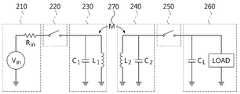
도 1을 참조하면, 무선 전력 전송 시스템은 소스와 타겟으로 구성되는 소스-타겟 구조이다. 무선 전력 전송 시스템은 소스에 해당하는 무선 전력 전송 장치와 타겟에 해당하는 무선 전력 수신 장치를 포함할 수 있다.Referring to FIG. 1, a wireless power transmission system is a source-target structure consisting of a source and a target. The wireless power transmission system may include a wireless power transmission device corresponding to the source and a wireless power receiving device corresponding to the target.
무선 전력 전송 장치는 전력 입력부(110), 전력 전송부(120) 및 스위치부(130)를 포함한다. 전력 입력부(110)는 전원 공급 장치를 이용하여 캐패시터에 에너지를 저장한다. 스위치부(130)는 캐패시터에 에너지가 저장되는 동안에는 전력 입력부(110)에 캐패시터를 연결하고, 스위치부(130)는 캐패시터에 저장된 에너지를 방전하는 동안에는 캐패시터를 전력 전송부(120)에 연결한다. 즉, 스위치부(130)는 캐패시터가 동시에 전력 입력부(110) 및 전력 전송부(120)에 연결되지 않도록 한다.The wireless power transmission apparatus includes a
전력 전송부(120)는 전자기(electromagnetic) 에너지를 수신부(140)로 전달(transferring)한다. 보다 구체적으로 전력 전송부(120)는 전력 전송부(120)의 소스 공진기와 수신부(130)의 타겟 공진기 간의 상호 공진을 통해 전력을 전달할 수 있다. 이때, 소스 공진기는 캐패시터(C1) 및 송신 코일(L1)을 포함할 수 있고, 타겟 공진기는 캐패시터(C2) 및 수신 코일(L2)을 포함할 수 있다. 소스 공진기와 타겟 공진기 간에 발생하는 상호 공진의 정도는 상호 인덕턴스 M의 영향을 받는다.The power transmitting
전력 입력부(110)는 입력 전압(VDC), 내부 저항(Rin) 및 캐패시터(C1)로, 전력 전송부(120)는 기초 회로 소자(R1, L1, C1)로, 스위치부(130)는 적어도 하나의 스위치로 모델링 될 수 있다. 캐패시터(C1)는 스위치부(130)의 동작에 따라 전력 입력부(110)에 속하기도 하고, 전력 전송부(120)에 속하기도 한다. 스위치로는 온/오프 기능을 수행할 수 있는 능동소자가 사용될 수 있다. R은 저항 성분, L은 인덕터 성분, C는 캐패시터 성분을 의미한다. 입력 전압(VDC) 중 캐패시터(C1)에 걸리는 전압은 Vin으로 표시될 수 있다.The
무선 전력 수신 장치는 수신부(140), 전력 출력부(150) 및 스위치부(160)를 포함한다. 수신부(140)는 전력 전송부(120)로부터 전자기(electromagnetic) 에너지를 수신한다. 수신부(140)는 수신한 전자기 에너지를 연결된 캐패시터들에 저장한다. 스위치부(160)는 수신부(140)에 캐패시터를 연결하여 캐패시터에 에너지를 저장하고, 스위치부(160)는 캐패시터를 전력 출력부(150)에 연결하여 캐패시터에 저장된 에너지를 부하에 전달할 수 있다. 즉, 스위치부(160)는 캐패시터가 동시에 수신부(140) 및 전력 출력부(150)에 연결되지 않도록 한다.The wireless power receiving apparatus includes a
보다 구체적으로 수신부(140)의 수신 코일(L2)은 전력 전송부(120)의 송신 코일(L1)과의 상호 공진을 통하여 전력을 수신할 수 있다. 수신된 전력을 통하여 수신 코일(L2)과 연결된 캐패시터가 충전될 수 있다. 전력 출력부(150)는 캐패시터에 충전된 전력을 배터리로 전달한다. 전력 출력부(150)는 배터리 대신, 부하 또는 타겟 디바이스에 전력을 전달할 수 있다.More specifically, the receiving coil L2 of the receiving
수신부(140)는 기초 회로 소자(R2, L2,C2)로, 전력 출력부(150)는 연결되는 캐패시터(C2) 및 배터리로, 스위치부(160)는 적어도 하나의 스위치로 모델링 될 수 있다. 캐패시터(C2)는 스위치부(160)의 동작에 따라 수신부(140)에 속하기도 하고, 전력 출력부(150)에 속하기도 한다.수신 코일(L2)에서 수신되는 에너지 중, 캐패시터(C2)에 걸리는 전압은 Vout으로 표시될 수 있다.The receiving
위와 같이 전력 입력부(110)와 전력 전송부(120)를 물리적으로 분리하고, 수신부(140)와 전력 출력부(150)를 물리적으로 분리하여 전력을 전송하는 RI(Resonator Isolation) 시스템은 임피던스 매칭을 사용한 기존의 전력 전송 방식에 비하여 여러 가지의 장점을 가진다. 첫째, DC 전원으로부터 소스 공진기에 직접 전력 공급이 가능하기 때문에, 전력 증폭기를 사용하지 않을 수 있다. 둘째, 배터리의 충전을 위해 수신단의 캐패시터에 충전된 전력에서 에너지를 채득(capture)하기 때문에, 정류기를 통한 정류작업이 필요 없다. 셋째, 임피던스 매칭을 할 필요가 없으므로 전송 효율이 송신단과 수신단 사이의 거리변화에 민감하지 않다. 또한, 복수의 송신단 및 복수의 수신단을 포함하는 무선 에너지 전송 시스템으로의 확장이 용이하다.An RI (Resonator Isolation) system that physically separates the
도 2는 다른 일실시예에 따른 무선 전력 전송 시스템의 등가회로를 나타낸 도면이다. 도 2는 RI(Resonator Isolation) 시스템의 다른 예이다.2 is a diagram illustrating an equivalent circuit of a wireless power transmission system according to another embodiment. Figure 2 is another example of a Resonator Isolation (RI) system.
도 2를 참조하면, 무선 전력 전송 시스템은 소스와 타겟으로 구성되는 소스-타겟 구조이다. 즉, 무선 전력 전송 시스템은 소스에 해당하는 무선 전력 전송 장치와 타겟에 해당하는 무선 전력 수신 장치를 포함한다.Referring to FIG. 2, a wireless power transmission system is a source-target structure composed of a source and a target. That is, the wireless power transmission system includes a wireless power transmission device corresponding to a source and a wireless power receiving device corresponding to a target.
무선 전력 전송 장치는 전력 충전부(210), 제어부(220) 및 전송부(230)를 포함할 수 있다. 전력 충전부(210)는 전원 공급 장치(Vin)와 저항(Rin)으로 구성될 수 있다. 소스 공진기는 캐패시터(C1)와 인덕터(L1)로 구성될 수 있다. 전송부(230)는 소스 공진기와 타겟 공진기 간의 상호 공진을 통하여 소스 공진기에 저장된 에너지를 전송할 수 있다. 제어부(220)는 전력 충전부(210)로부터 소스 공진기에 전력을 공급하기 위해 스위치를 온(on) 할 수 있다. 전원 공급 장치(Vin)로부터 캐패시터(C1)에 전압이 인가되고, 인덕터(L1)에 전류가 인가될 수 있다. 소스 공진기가 정상 상태에 도달하게 되면, 캐패시터(C1)에 인가되는 전압은 0이 되고, 인덕터(L1)에 흐르는 전류는 Vin/ Rin의 값을 가지게 된다. 정상 상태에서는 인덕터(L1)에 인가되는 전류를 통하여 인덕터(L1)에 전력이 충전된다.The wireless power transmission apparatus may include a
제어부(220)는 정상 상태에서 소스 공진기에 충전된 전력이 소정 값에 도달하면, 스위치를 오프(off)할 수 있다. 소정 값에 대한 정보는 제어부(220)에 미리 설정될 수 있다. 전력 충전부(210)와 전송부(230)는 스위치 동작에 의해 분리된다. 스위치가 오프 되면, 소스 공진기는 캐패시터(C1)와 인덕터(L1)간에 자체 공진을 시작한다. 또한, 상호 인덕턴스 M(270)의 영향을 받는 소스 공진기와 타겟 공진기 간의 상호 공진을 통하여, 소스 공진기에 저장된 에너지는 타겟 공진기로 전달될 수 있다. 이때, 소스 공진기의 공진 주파수(f1)와 타겟 공진기의 공진 주파수(f2)는 동일하다. 소스 공진기의 공진 주파수(f1)와 타겟 공진기의 공진 주파수(f2)는 [수학식 1]을 통해서 계산될 수 있다.The
[수학식 1][Equation 1]

무선 전력 수신 장치는 충전부(240), 제어부(250) 및 전력 출력부(260)를 포함할 수 있다. 타겟 공진기는 캐패시터(C2)와 인덕터(L2)로 구성될 수 있다. 소스 공진기와 타겟 공진기 간에 상호 공진을 할 때는 소스 공진기는 전원 공급 장치(Vin)와 분리되어 있고, 타겟 공진기는 부하(LOAD) 및 캐패시터(CL)와 분리되어 있다. 타겟 공진기의 캐패시터(C2)와 인덕터(L2)는 상호 공진을 통하여 전력을 충전할 수 있다. 제어부(250)는 타겟 공진기에 전력을 충전하기 위해, 스위치를 오프(off)할 수 있다. 스위치가 오프인 동안, 타겟 공진기의 공진 주파수와 소스 공진기의 공진 주파수는 일치하여, 상호 공진이 발생할 수 있다. 제어부(250)는 타겟 공진기에 충전된 전력이 소정 값에 도달하면, 스위치를 온(on)할 수 있다. 소정 값에 대한 정보는 제어부(250)에 미리 설정될 수 있다. 스위치가 온 되면, 캐패시터(CL)이 연결되어, 타겟 공진기의 공진 주파수가 [수학식 2]와 같이 변경된다.The wireless power receiving apparatus may include a
[수학식 2]&Quot; (2) "

따라서, 소스 공진기와 타겟 공진기 간의 공진 주파수가 일치하지 않게 되고, 소스 공진기와 타겟 공진기 간에 상호 공진이 종료된다. 보다 구체적으로는 타겟 공진기의 Q를 고려하여, f2'이 f2보다 충분히 작다면, 상호 공진 채널이 소멸할 수 있다. 또한, 전력 출력부(260)는 캐패시터(C2)와 인덕터(L2)에 충전된 전력을 부하(LOAD)에 전달할 수 있다. 전력 출력부(260)는 부하(LOAD)의 필요에 적합한 방식으로 전력을 전달할 수 있다. 예를 들면, 전력 출력부(260)는 부하에서 요구하는 정격 전압으로 전압을 레귤레이션(regulation)하여 전력을 전달할 수 있다.Therefore, the resonance frequencies between the source resonator and the target resonator do not coincide with each other, and mutual resonance ends between the source resonator and the target resonator. More specifically, in consideration of Q of the target resonator, if f2 'is sufficiently smaller than f2 , mutual resonance channels may disappear. Also, the
제어부(250)는 타겟 공진기에 충전된 전력이 소정 값 미만의 값을 갖게 되면, 스위치를 오프(off)할 수 있다. 오프(off)로 인하여 소스 공진기와 타겟 공진기의 공진 주파수가 다시 일치하게 되면, 충전부(240)는 소스 공진기와 타겟 공진기 간의 상호 공진을 통하여 다시 타겟 공진기에 전력을 충전할 수 있다.The
소스 공진기와 타겟 공진기 간에 상호 공진이 발생할 때는 스위치가 연결되지 않는다. 따라서, 스위치의 연결에 따른 전송 효율의 감소가 예방될 수 있다.When mutual resonance occurs between the source resonator and the target resonator, no switch is connected. Therefore, a decrease in transmission efficiency due to the connection of the switches can be prevented.
도 1의 캐패시터에 충전된 에너지를 전달하는 방식에 비해, 도 2의 방식은 타겟 공진기에 저장된 에너지의 채득(capture) 시점을 제어하는 것이 좀 더 용이하다. 도 1의 캐패시터에 충전된 에너지를 전달하는 방식에서는 무선 전력 수신 장치가 캐패시터에 충전된 에너지를 채득(capture) 할 수 있지만, 도 2의 공진 주파수를 변경하여 에너지를 채득하는 방식은 타겟 공진기의 인덕터 및 캐패시터에 저장된 에너지를 채득하므로, 에너지의 채득 시점에 대한 자유도가 향상된다.2, it is easier to control the capture time of the energy stored in the target resonator than in the method of transferring the charged energy to the capacitor of FIG. In the method of transferring the energy charged in the capacitor of FIG. 1, the wireless power receiving apparatus can capture the energy charged in the capacitor. However, in the method of changing the resonance frequency of FIG. 2 to generate energy, And the energy stored in the capacitor, so that the degree of freedom with respect to the point of time at which the energy is collected is improved.
RI(Resonator Isolation) 시스템의 송신단은 전력 혹은 데이터의 전송을 위해, 스위치의 연결을 통해 소스 공진기에 에너지의 충전과 방전을 반복 수행한다. 이러한 한 번의 에너지의 충전과 방전 과정은 하나의 심볼로 정의될 수 있다. 수신단은 송신단으로부터 에너지 또는 데이터를 수신하기 위해, 송신단의 충전 및 방전을 반복하는 스위치의 동작 주기에 맞추어, 수신단의 스위치를 동작시켜야 한다.The transmitting end of the RI (Resonator Isolation) system repeatedly performs charging and discharging of energy to the source resonator through the connection of the switch for transmission of power or data. This single charge and discharge process of energy can be defined as a single symbol. In order to receive energy or data from the transmitting end, the receiving end must operate the switch of the receiving end in accordance with the operation cycle of the switch for repeating charging and discharging of the transmitting end.
수신단은 송신단으로부터 오류 없이 전력 또는 데이터를 수신하기 위해, 송신단의 스위치가 언제 오프(off)되고 언제 온(on)되는지, 그리고 언제 상호 공진을 시작하고, 언제 타겟 공진기에 저장된 에너지가 피크 값을 가지는지 알 필요가 있다. 송신단 스위치의 온/오프 타임에 대한 정보를 알아내고, 수신단의 온/오프 타임을 송신단 스위치의 온/오프 타임에 대한 정보에 맞게 조절하는 과정을 시간 동기화 과정이라고 정의할 수 있다.In order to receive power or data without error from the transmitting end, the receiving end must know when the transmitting end switch is turned off and when it starts, when the mutual resonance starts, and when the energy stored in the target resonator has a peak value You need to know. Off time of the transmitting end switch and adjusting the on / off time of the receiving end to the information of the on / off time of the transmitting end switch can be defined as a time synchronization process.
RI system은 정보를 전달하기 위하여, 소스 공진기와 타겟 공진기 간의 상호 공진 현상을 이용한다. 보다 구체적으로, 송신단은 상호 약속된 정해진 시간 구간 동안 전원으로부터 소스 공진기로 에너지를 주입하거나/주입하지 않는 동작을 통해 해당 시간 구간 동안 상호 공진을 일으키거나/일으키지 아니하는 현상을 유도할 수 있고, 각각의 현상에 정보를 할당(assign)할 수 있다. 예를 들면, 송신단은 상호 공진이 발생하는 현상에 비트 1을, 상호 공진이 발생하지 않는 현상에 비트 0을 할당할 수 있다. 여기서 정해진 시간 구간은 예를 들면, 하나의 심볼로 정의될 수 있다.The RI system uses the mutual resonance phenomenon between the source resonator and the target resonator to transmit information. More specifically, the transmitting end can induce a phenomenon that causes / does not cause mutual resonance during the time interval through the operation of injecting / not injecting energy from the power source into the source resonator for a predetermined fixed time interval, The user can assign information to the phenomenon of < RTI ID = 0.0 > For example, the transmitting end can allocate
수신단은 정해진 시간 구간 동안, 타겟 공진기의 공진주파수를 소스 공진기의 공진주파수와 맞추거나/맞추지 아니하는 동작으로 상호 공진을 일으키거나/일으키지 아니하는 현상을 유도할 수 있다. 이때, 수신단은 각각의 현상에 정보를 할당(assign)할 수 있다. 예를 들면, 수신단은 상호 공진이 발생하는 현상에 비트 1을, 상호 공진이 발생하지 않는 현상에 비트 0을 할당할 수 있다.The receiving end can induce a phenomenon in which the resonance frequency of the target resonator is caused to coincide with the resonance frequency of the source resonator and / or not to cause mutual resonance during the predetermined time period. At this time, the receiving end can assign information to each phenomenon. For example, the receiving end can assign
심볼 단위로 정보를 전달하는 방법에 있어서, 심볼의 동기를 맞추는 작업이 선행되어야 한다. 심볼의 동기를 맞추기 위해 수신단 또는 송신단에서 동기 정합 작업을 수행할 수 있다. 동기 정합 작업이 이루어지면, 사전에 정해진 프로토콜에 의해 송신단과 수신단 간에 양방향 데이터 전송이 이루어질 수 있다.
In the method of transmitting information on a symbol-by-symbol basis, synchronization of symbols must be preceded. A synchronous matching operation can be performed at the receiving end or the transmitting end to synchronize the symbols. When the synchronous matching operation is performed, bidirectional data transmission can be performed between the transmitting end and the receiving end according to a predetermined protocol.
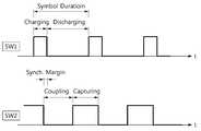
도 3은 일실시예에 따른 무선 전력 전송 시스템에서 송신단과 수신단의 스위치의 동작 타이밍을 나타낸 도면이다.3 is a diagram illustrating operation timings of switches of a transmitter and a receiver in a wireless power transmission system according to an embodiment.
도 3을 참조하면, 송신단은 충전(charging)과 방전(discharging) 과정의 반복을 통해 수신단으로 에너지를 전송한다. 이러한 한 번의 에너지의 충전과 방전 과정은하나의 심볼로 정의될 수 있다.Referring to FIG. 3, the transmitter transmits energy to the receiver through repetition of charging and discharging. This single charge and discharge process of energy can be defined as a single symbol.
도 2의 RI 시스템을 고려하면, 수신단은 송신단에서 전송하는 에너지를 수신하기 위해 송신단의 SW1이 오프(off)되어, 방전단계로 전환하기 소정의 시간(Sync. Margin) 이전에, SW2를 오프(off)하여 송신단과의 상호 공진을 준비한다.Considering the RI system of FIG. 2, the receiving end of the transmitting terminal SW1 is turned off to receive the energy transmitted from the transmitting end, and SW2 is turned off before a predetermined time (Sync. off to prepare mutual resonance with the transmitting end.
상호 공진이 시작되면, 수신단의 타겟 공진기에 에너지가 충전된다. 상호 공진은 소스 공진기와 타겟 공진기 간의 커플링(coupling)으로 표현될 수 있다. 수신단은 타겟 공진기에 저장되는 에너지가 피크 값을 가지는 시점에, SW2를 온(on)하여, 타겟 공진기의 공진 주파수를 소스 공진기의 공진 주파수와 다르게 변경하고, 타겟 공진기에 저장된 에너지를 채득(capturing)할 수 있다. 수신단은 타겟 공진기에 저장되는 에너지의 값에 기초하여 SW2의 온/오프 시점을 조절함으로써, 송신단의 SW1과의 동기를 정합할 수 있다.When mutual resonance is started, the target resonator of the receiving end is charged with energy. The mutual resonance can be expressed by the coupling between the source resonator and the target resonator. At the time when the energy stored in the target resonator has a peak value, the receiving end turns ON the switch SW2, changes the resonance frequency of the target resonator to be different from the resonance frequency of the source resonator, captures the energy stored in the target resonator, can do. The receiving end can match the synchronization with the SW1 of the transmitting end by adjusting the on / off point of the SW2 based on the value of the energy stored in the target resonator.
RI 시스템의 송신단에서, 소스 공진기에 에너지를 주입하기 위한 소스 공진기와 전원의 연결 및 공진 현상의 유도를 위한 소스 공진기와 전원의 연결 개방(disconnect)은 전원과 소스 공진기 사이의 스위치에 의해 수행된다.In the transmitting end of the RI system, the connection between the source resonator and the power source for inducing resonance phenomenon is performed by a switch between the power source and the source resonator.
또한 RI 시스템의 수신단에서, 타겟 공진기의 고립(isolation)을 통한 소스 공진기와의 상호 공진 및 타겟 공진기와 소스 공진기 간의 공진 주파수 분리 등의 동작도 스위치에 의해 수행된다.Also, at the receiving end of the RI system, mutual resonance with the source resonator through isolation of the target resonator and resonance frequency separation between the target resonator and the source resonator are also performed by the switch.
에너지 및 데이터를 전송하기 위한 RI 시스템의 기본 동작 및 성능은 스위칭 회로에 의해 많은 부분이 결정 된다. 예를 들면, 소스 공진기로부터 타겟 공진기로 전송되는 전력량을 늘리기 위해서는 스위치가 닫힌 상태, 즉 연결된 상태에서 충분히 많은 양의 전류를 소스 공진기로 흘려 줄 수 있어야 한다. 또한, 스위치가 열린 상태, 즉 연결이 끊어진 상태에서 스위치의 양단이 전기적으로 완전히 분리되어야 한다. 또한, 빠른 데이터의 전송을 위해서는 스위치의 턴 온(turn on) 및 턴 오프(turn off)에 걸리는 전이(transient) 시간 또한 충분히 짧아야 한다.The basic operation and performance of the RI system for transmitting energy and data is largely determined by the switching circuitry. For example, in order to increase the amount of power transmitted from the source resonator to the target resonator, a sufficiently large amount of current must be allowed to flow to the source resonator in a closed state, that is, in a connected state. In addition, both ends of the switch must be completely electrically disconnected when the switch is open, i.e., disconnected. Also, for fast data transmission, the transient time to turn on and turn off of the switch must also be sufficiently short.
또한, 많은 양의 에너지가 소스 공진기에 주입되는 경우, 소스 공진기 내에서 공진하는 신호의 진폭이 커진다. 이때, 큰 진폭의 신호를 차단하기 위해서는 일반적으로 스위치에 인가해 주는 전원 또한 높은 진폭의 전압 값을 가질 필요가 있다. 따라서, 일반적인 스위치를 사용하는 경우, 큰 진폭의 신호를 차단하기 위해서 높은 전압의 출력을 가지는 전원이 필요하고, 이로 인해 시스템의 복잡도가 올라가며, 소모 전력 또한 증가하게 된다.Further, when a large amount of energy is injected into the source resonator, the amplitude of the resonating signal in the source resonator becomes large. In this case, in order to cut off a signal having a large amplitude, it is generally necessary to have a voltage having a high amplitude to supply power to the switch. Therefore, when a general switch is used, a power supply having a high voltage output is required in order to cut off a signal having a large amplitude, thereby increasing the complexity of the system and increasing the power consumption.
스위치는 CMOS(Complementary Metal Oxide Semiconductor)를 통해 일반적으로 구현이 될 수 있다. CMOS로 구현된 스위치의 V+ 및 V- 전원과 VIN 은 스위치의 입력 및 출력 신호의 진폭에 따라 달라질 수 있다. 예를 들며, -10V에서 +10V까지의 진폭을 가지는 입력과 출력 신호에 대해 스위치 ON 및 OFF 동작을 수행하기 위해서는 +10V 이상의 V+ 와 -10V 이하의 V-, 그리고 10V 이상의 VIN 값이 요구된다.
Switches can be implemented generally through CMOS (Complementary Metal Oxide Semiconductor). The V + and V-powers of the switch implemented in CMOS and VIN may vary depending on the amplitude of the input and output signals of the switch. For example, to perform switch ON and OFF operations on input and output signals with amplitudes from -10V to + 10V, a V + value of + 10V or more, a V- of -10V or less, and a VIN value of 10V or more are required .
도 4는 일실시예에 따른 무선 전력 전송 장치의 블록도이다.4 is a block diagram of a wireless power transmission apparatus according to an embodiment.
도 4를 참조하면, 일실시예에 따른 무선 전력 전송 장치는 전원 공급부(410), 스위칭부(420), 소스 공진기(430) 및 제어부(440)를 포함할 수 있다.Referring to FIG. 4, a wireless power transmission apparatus according to an embodiment may include a
전원 공급부(410)는 소스 공진기(430)로 전력을 공급할 수 있다. 전원 공급부(410)는 직류 전압을 공급할 수도 있고, 직류 전류를 공급할 수도 있다. 전원 공급부(410)는 스위칭부(420)를 통하여 소스 공진기(430)와 연결되는 경우에 전력을 공급할 수 있다.The
스위칭부(420)는 제어 신호에 기초하여 전원 공급부(410)와 소스 공진기(430)를 연결할 수 있다. 스위칭부(420)는 제어 신호에 따라 턴 온(turn on) 또는 턴 오프(turn off) 동작을 수행할 수 있다. 턴 온 상태에서, 전원 공급부(410)와 소스 공진기(430)는 연결되고, 턴 오프 상태에서, 전원 공급부(410)와 소스 공진기(430)의 연결은 끊어진다. 스위칭부(530)를 턴 온 또는 턴 오프 시키는 제어 신호의 값은 스위칭부(420)를 구성하는 트랜지스터(421)의 종류에 따라 다양한 값으로 설정될 수 있다.The
소스 공진기(430)는 타겟 공진기(도시되지 않음)와의 상호 공진을 통하여 전력을 전송할 수 있다.The
스위칭부(420)는 트랜지스터(421) 및 다이오드(423)를 포함할 수 있다. 트랜지스터(421)와 다이오드(423)는 직렬로 연결된다. 다이오드(423)는 트랜지스터(421)의 전단 또는 후단 어디에나 위치할 수 있다. 도 4의 예에서는 스위칭부(420)가 무선 전력 전송 장치에 사용되었지만, 다른 예로 무선 전력 수신 장치에 사용될 수도 있다.The
트랜지스터(421)는 제어 신호의 값과 기준 값을 비교한 결과에 기초하여 전원 공급부(410)와 소스 공진기(430)의 연결을 턴 온(turn on) 또는 턴 오프(turn off)할 수 있다. 트랜지스터(421)의 종류에 따라 제어 신호의 값이 기준 값보다 작은 경우에 턴 온 동작을 수행하는 경우가 있고, 제어 신호의 값이 기준 값보다 크거나 같은 경우에 턴 온 동작을 수행하는 경우가 있다. 또한, 트랜지스터(421)의 종류에 따라 제어 신호의 값이 기준 값보다 크거나 같은 경우에 턴 오프 동작을 수행하는 경우가 있고, 제어 신호의 값이 기준 값보다 작은 경우에 턴 오프 동작을 수행하는 경우가 있다.The
다이오드(423)는 트랜지스터(421)와 직렬로 연결된다. 트랜지스터(421) 및 다이오드(423)는 턴 온 상태에서 전원 공급부(410)의 직류 신호를 통과시키고, 턴 오프 상태에서 소스 공진기(430)로부터 교류 신호의 유입을 차단할 수 있다.
턴 오프 상태에서는 소스 공진기(430)에서 자기 공진 및 상호 공진이 발생하여 교류 신호가 생성될 수 있다. 이때, 교류 신호에는 교류 전류 신호 및 교류 전압 신호가 포함된다. 소스 공진기(430)의 교류 전류 신호의 플러스 성분이 다이오드(423)에 인가되는 경우, 교류 전류 신호의 플러스 성분이 다이오드(423)에 의해 차단되어 트랜지스터(421) 방향으로 유입되지 않을 수 있다. 또한, 소스 공진기(430)의 교류 전류 신호의 마이너스 성분이 다이오드(423)에 인가되는 경우, 트랜지스터(421)가 턴 오프 상태로 동작하므로, 교류 전류 신호의 마이너스 성분이 트랜지스터(421)에 의해 차단되어 트랜지스터(421) 방향으로 유입되지 않을 수 있다. 따라서, 트랜지스터(421)의 양단이 전기적으로 완전히 분리될 수 있다.In the turn-off state, self resonance and mutual resonance occur in the
제어부(440)는 제어 신호를 생성하고, 제어 신호의 진폭 및 주기를 제어할 수 있다. 제어부(440)는 트랜지스터(421)의 턴 온 또는 턴 오프 동작에 필요한 크기로 제어 신호의 진폭을 제어할 수 있다. 또한, 제어부(440)는 트랜지스터(421)를 턴 온 시킨 후에도, 제어 신호의 진폭을 조절함으로써 전원 공급부(410)로부터 소스 공진기(430)로 전달하는 전력의 량을 조절할 수 있다. 제어 신호의 진폭이 조절됨에 따라 트랜지스터(421)에서 전류가 이동할 수 있는 채널의 두께가 조절될 수 있다. 다시 말해서, 제어 신호의 진폭이 조절됨에 따라 트랜지스터(421)의 저항 값이 변할 수 있다. 따라서, 트랜지스터(421)의 저항 값이 변함에 따라 소스 공진기(430)로 전달되는 전력의 량도 변할 수 있다.The
예를 들면, 트랜지스터(421)가 MOS(Metal Oxide Semiconductor) 타입인 경우에, 제어부(440)는 MOS의 게이트(Gate)에 인가하는 전압의 진폭을 조절함으로써, 전원 공급부(410)로부터 소스 공진기(430)로 전달하는 전력의 량을 조절할 수 있다.For example, when the
제어부(440)는 소스 공진기(430)로 전달하려는 에너지의 양에 따라 제어 신호의 주기를 제어할 수 있다. 예를 들면, 소스 공진기(430)로 전달하려는 전류의 양을 증가시키려면, 제어부(440)는 트랜지스터(421)를 턴 온 시키는 제어신호의 주기를 길게 할 수 있다. 예를 들면, 제어 신호는 펄스파 또는 구형파의 모양을 가질 수 있다. 또한, 반대로 소스 공진기(430)로 전달하려는 전류의 양을 감소시키려면, 제어부(440)는 트랜지스터(421)를 턴 온 시키는 제어신호의 주기를 짧게 할 수 있다.The
일 실시예로, 트랜지스터(421)가 피모스(PMOS, P-channel Metal Oxide Semiconductor)인 경우, 제어 신호는 피모스의 게이트에 인가된다. 이때, 제어 신호는 전압 신호일 수 있다.In one embodiment, when the
게이트에 인가되는 제어 신호의 전압이 피모스의 소스(Source)에 인가되는 전압과 피모스의 문턱전압의 차이보다 작거나 같으면, 피모스는 전원 공급부(410)와 소스 공진기(430)의 연결을 턴 온(turn on)시킬 수 있다.If the voltage of the control signal applied to the gate is less than or equal to the difference between the voltage applied to the source of the PMOS and the threshold voltage of the PMOS, the PMOS is connected to the
게이트에 인가되는 제어 신호의 전압이 피모스의 소스에 인가되는 전압과 피모스의 문턱전압의 차이보다 커지면, 피모스는 전원 공급부(410)와 소스 공진기(430)의 연결을 턴 오프(turn off)시킬 수 있다.When the voltage of the control signal applied to the gate is larger than the difference between the voltage applied to the source of the PMOS and the threshold voltage of the PMOS, the PMOS turns off the connection between the
여기서, 트랜지스터(421)를 턴 온 또는 턴 오프 시키는 기준 값은 피모스의 소스에 인가되는 전압과 피모스의 문턱전압의 차이에 해당하는 값이다. 즉, 제어 신호의 전압이 위 기준 값보다 작거나 같으면, 트랜지스터(421)는 턴 온 되고, 제어 신호의 전압이 위 기준 값보다 크면, 트랜지스터(421)는 턴 오프 된다.Here, the reference value for turning the
일반적인 스위치는 입출력 신호의 전압보다 큰 바이어스 전압과 입출력 신호의 전압보다 큰 구동전압이 필요하다는 점에 비추어 볼 때, 트랜지스터(421)는 제어 신호가 기준 값보다 크거나 작은지에 따라 턴 온/턴 오프가 결정됨으로써, 제어 신호의 전압이 입출력 신호의 영향에 민감하지도 않고, 전압이 큰 값을 가질 필요도 없다.In view of the fact that a general switch requires a driving voltage larger than the voltage of the input / output signal and the bias voltage larger than the voltage of the input / output signal, the
다이오드(423)는 피모스와 직렬로 연결된다. 다이오드(423)는 피모스의 소스(Source)와 직렬로 연결될 수도 있고, 피모스의 드레인(Drain)과 직렬로 연결될 수도 있다.
피모스 및 다이오드(423)는 피모스에서 턴 온의 상태가 유지되는 동안 전원 공급부(410)로부터 공급하는 직류 전류 신호를 통과시킬 수 있다. 피모스에서 턴 온의 상태가 유지되는 동안 다이오드(423)에는 순방향 바이어스가 인가된다.The PMOS and the
피모스 및 다이오드(423)는 피모스에서 턴 오프의 상태가 유지되는 동안 소스 공진기(430)로부터 교류 전류 신호의 유입을 차단할 수 있다. 피모스에서 턴 오프의 상태가 유지되는 동안, 소스 공진기(430)에서는 교류 전류 신호가 발생할 수 있다. 교류 전류 신호의 플러스 성분은 다이오드(423)에 의해 유입이 차단되며, 교류 전류 신호의 마이너스 성분은 피모스에 의해 유입이 차단될 수 있다. 이때, 교류 전류 신호의 플러스 성분이 다이오드(423)에 인가될 때에는 다이오드(423)에는 역방향 바이어스가 인가된다.The PMOS and
다른 일 실시예로, 트랜지스터(421)가 엔모스(NMOS, N-channel Metal Oxide Semiconductor)인 경우, 제어 신호는 엔모스의 게이트에 인가된다. 이때, 제어 신호는 전압 신호일 수 있다.In another embodiment, when the
게이트에 인가되는 제어 신호의 전압이 엔모스의 소스(Source)에 인가되는 전압과 엔모스의 문턱전압의 합보다 크거나 같으면, 엔모스는 전원 공급부(410)와 소스 공진기(430)의 연결을 턴 온(turn on)시킬 수 있다. 또는 게이트에 인가되는 제어 신호의 전압이 엔모스의 드레인(drain)에 인가되는 전압과 엔모스의 문턱전압의 합보다 크거나 같으면, 엔모스는 전원 공급부(410)와 소스 공진기(430)의 연결을 턴 온(turn on)시킬 수 있다.If the voltage of the control signal applied to the gate is greater than or equal to the sum of the voltage applied to the source of the emmos and the threshold voltage of the emmos, the emmos will be connected to the
게이트에 인가되는 제어 신호의 전압이 엔모스의 소스에 인가되는 전압과 엔모스의 문턱전압의 합보다 작아지면, 엔모스는 전원 공급부(410)와 소스 공진기(430)의 연결을 턴 오프(turn off)시킬 수 있다. 또는 게이트에 인가되는 제어 신호의 전압이 엔모스의 드레인에 인가되는 전압과 엔모스의 문턱전압의 합보다 작아지면, 엔모스는 전원 공급부(410)와 소스 공진기(430)의 연결을 턴 오프(turn off)시킬 수 있다.When the voltage of the control signal applied to the gate becomes smaller than the sum of the voltage applied to the source of the emmos and the threshold voltage of the emmos, the emmos turns off the connection between the
여기서, 트랜지스터(421)를 턴 온 또는 턴 오프 시키는 기준 값은 엔모스의 소스에 인가되는 전압과 엔모스의 문턱전압의 합에 해당하는 값이다. 또는 기준 값은 엔모스의 드레인에 인가되는 전압과 엔모스의 문턱전압의 합에 해당하는 값이다. 즉, 제어 신호의 전압이 위 기준 값보다 크거나 같으면, 트랜지스터(421)는 턴 온 되고, 제어 신호의 전압이 위 기준 값보다 작으면, 트랜지스터(421)는 턴 오프 된다.Here, the reference value for turning on or off the
다이오드(423)는 엔모스의 소스(Source)와 직렬로 연결된다. 다이오드(423)는 엔모스의 소스(Source)와 직렬로 연결될 수도 있고, 엔모스의 드레인(Drain)과 직렬로 연결될 수도 있다.The
엔모스 및 다이오드(423)는 엔모스에서 턴 온의 상태가 유지되는 동안 전원 공급부(410)로부터 공급하는 직류 전류 신호를 통과시킬 수 있다. 엔모스에서 턴 온의 상태가 유지되는 동안 다이오드(423)에는 순방향 바이어스가 인가된다.The NMOS and the
엔모스 및 다이오드(423)는 엔모스에서 턴 오프의 상태가 유지되는 동안 소스 공진기(430)로부터 교류 전류 신호의 유입을 차단할 수 있다. 엔모스에서 턴 오프의 상태가 유지되는 동안, 소스 공진기(430)에서는 교류 전류 신호가 발생할 수 있다. 교류 전류 신호의 플러스 성분은 다이오드(423)에 의해 유입이 차단되며, 교류 전류 신호의 마이너스 성분은 엔모스에 의해 유입이 차단될 수 있다. 이때, 교류 전류 신호의 플러스 성분이 다이오드(423)에 인가될 때에는 다이오드(423)에는 역방향 바이어스가 인가된다.And the
다른 일 실시예로, 트랜지스터(421)가 바이폴라 접합 트랜지스터(BJT, Bipolar Junction Transistor)인 경우, 트랜지스터는 바이폴라 접합 트랜지스터의 베이스(Base)에 인가되는 제어 신호의 전류 값에 기초하여 전원 공급부(410)와 소스 공진기(430)의 연결을 턴 온(turn on) 또는 턴 오프(turn off)할 수 있다.In another embodiment, when the
다이오드(423)는 바이폴라 접합 트랜지스터와 직렬로 연결된다. 다이오드(423)는 바이폴라 접합 트랜지스터의 컬렉터(Collector)와 직렬로 연결될 수도 있고, 이미터(Emitter)와 직렬로 연결될 수도 있다.
바이폴라 접합 트랜지스터 및 다이오드(423)는 바이폴라 접합 트랜지스터에서 턴 온의 상태가 유지되는 동안 전원 공급부(410)로부터 공급하는 직류 전류 신호를 통과시킬 수 있다.The bipolar junction transistor and the
바이폴라 접합 트랜지스터 및 다이오드(423)는 바이폴라 접합 트랜지스터 에서 턴 오프의 상태가 유지되는 동안 소스 공진기(430)로부터 교류 전류 신호의 유입을 차단할 수 있다. 바이폴라 접합 트랜지스터 에서 턴 오프의 상태가 유지되는 동안, 소스 공진기(430)에서는 교류 전류 신호가 발생할 수 있다. 교류 전류 신호의 플러스 성분은 다이오드(423)에 의해 유입이 차단되며, 교류 전류 신호의 마이너스 성분은 바이폴라 접합 트랜지스터에 의해 유입이 차단될 수 있다. 이때, 교류 전류 신호의 플러스 성분이 다이오드(423)에 인가될 때에는 다이오드(423)에는 역방향 바이어스가 인가된다.
The bipolar junction transistor and
도 5는 다른 일실시예에 따른 무선 전력 전송 장치의 블록도이다.5 is a block diagram of a wireless power transmission apparatus according to another embodiment.
도 5를 참조하면, 일실시예에 따른 무선 전력 전송 장치는 전원 공급부(510), 가변저항(520), 스위칭부(530), 소스 공진기(540) 및 제어부(550)를 포함할 수 있다.5, a wireless power transmission apparatus according to an exemplary embodiment of the present invention may include a
전원 공급부(510)는 소스 공진기(540)로 전력을 공급할 수 있다. 전원 공급부(510)는 직류 전압을 공급할 수도 있고, 직류 전류를 공급할 수도 있다. 전원 공급부(510)는 스위칭부(530)를 통하여 소스 공진기(540)와 연결되는 경우에 전력을 공급할 수 있다.The
가변저항(520)은 전원 공급부(510)와 스위칭부(530) 사이에 위치할 수 있다. 가변저항(520) 값에 따라 전원 공급부(510)로부터 소스 공진기(540)로 공급되는 전류의 량이 조절될 수 있다. 가변저항(520) 값은 제어부(550)에 의해 결정될 수 있다. 가변저항(520)의 값은 소스 공진기(540)로 공급하려는 전류량에 따라 결정될 수 있다.The
스위칭부(530)는 제어 신호에 기초하여 전원 공급부(510)와 소스 공진기(540)를 연결할 수 있다. 스위칭부(530)는 제어 신호에 따라 턴 온(turn on) 또는 턴 오프(turn off) 동작을 수행할 수 있다. 턴 온 상태에서, 전원 공급부(510)와 소스 공진기(540)는 연결되고, 턴 오프 상태에서, 전원 공급부(510)와 소스 공진기(540)의 연결은 끊어진다. 스위칭부(530)를 턴 온 또는 턴 오프 시키는 제어 신호의 값은 스위칭부(530)를 구성하는 트랜지스터의 종류에 따라 다양한 값으로 설정될 수 있다.The
소스 공진기(540)는 타겟 공진기(도시되지 않음)와의 상호 공진을 통하여 전력을 전송할 수 있다.The
제어부(550)는 제어 신호를 생성하고, 제어 신호의 진폭 및 주기를 제어할 수 있다. 제어부(550)는 트랜지스터의 턴 온 또는 턴 오프 동작에 필요한 크기로 제어 신호의 진폭을 제어할 수 있다. 제어부(550)는 소스 공진기(540)로 전달하려는 에너지의 양에 따라 제어 신호의 주기를 제어할 수 있다. 예를 들면, 소스 공진기(540)로 전달하려는 전류의 양을 증가시키려면, 제어부(550)는 트랜지스터를 턴 온 시키는 제어신호의 주기를 길게 할 수 있다. 예를 들면, 제어 신호는 펄스파 또는 구형파의 모양을 가질 수 있다.
The
도 6은 또 다른 일실시예에 따른 무선 전력 전송 장치의 블록도이다.6 is a block diagram of a wireless power transmission apparatus according to another embodiment.
도 6을 참조하면, 일실시예에 따른 무선 전력 전송 장치는 전원 공급부(610), 복수의 저항들(621, 623, 625), 스위치들(631, 633, 635), 스위칭부(640), 소스 공진기(650) 및 제어부(660)를 포함할 수 있다.6, a wireless power transmission apparatus according to an embodiment includes a
전원 공급부(610)는소스 공진기(650)로 전력을 공급할 수 있다. 전원 공급부(610)는 직류 전압을 공급할 수도 있고, 직류 전류를 공급할 수도 있다. 전원 공급부(610)는 스위칭부(640)를 통하여 소스 공진기(650)와 연결되는 경우에 전력을 공급할 수 있다.The
복수개의 저항들(621, 623, 625)은 전원 공급부(610)와 병렬로 연결된다. 스위치들(631, 633, 635)은 복수개의 저항들(621, 623, 625) 각각과 직렬로 연결된다. 복수개의 저항들(621, 623, 625) 중 스위칭부(640)와 연결되는 저항들의 개수에 따라 전원 공급부(510)로부터 소스 공진기(540)로 공급되는 전류의 량이 조절될 수 있다. 복수개의 저항들(621, 623, 625)은 서로 동일한 저항 값을 가질 수도 있고, 서로 다른 저항 값을 가질 수도 있다. 복수개의 저항들(621, 623, 625) 중 스위칭부(640)와 연결되어야 할 저항은 제어부(550)에 의해 결정될 수 있다. 제어부(550)는 스위치들(631, 633, 635)을 제어하여, 복수개의 저항들(621, 623, 625) 중 적어도 하나의 저항을 스위칭부(640)와 연결할 수 있다.The plurality of
스위칭부(640)는 제어 신호에 기초하여 전원 공급부(610)와 소스 공진기(650)를 연결할 수 있다. 스위칭부(640)는 제어 신호에 따라 턴 온(turn on) 또는 턴 오프(turn off) 동작을 수행할 수 있다. 턴 온 상태에서, 전원 공급부(610)와 소스 공진기(650)는 연결되고, 턴 오프 상태에서, 전원 공급부(610)와 소스 공진기(650)의 연결은 끊어진다. 스위칭부(640)를 구성하는 트랜지스터의 종류에 따라 다양한 값으로 설정될 수 있다.The
소스 공진기(650)는 타겟 공진기(도시되지 않음)와의 상호 공진을 통하여 전력을 전송할 수 있다.The
제어부(660)는 제어 신호를 생성하고, 제어 신호의 진폭 및 주기를 제어할 수 있다. 제어부(660)는 트랜지스터의 턴 온 또는 턴 오프 동작에 필요한 크기로 제어 신호의 진폭을 제어할 수 있다. 제어부(660)는 소스 공진기(650)로 전달하려는 에너지의 양에 따라 제어 신호의 주기를 제어할 수 있다. 예를 들면, 소스 공진기(650)로 전달하려는 전류의 양을 증가시키려면, 제어부(660)는 트랜지스터를 턴 온 시키는 제어신호의 주기를 길게 할 수 있다. 예를 들면, 제어 신호는 펄스파 또는 구형파의 모양을 가질 수 있다.
The
도 7은 일실시예에 따른 무선 전력 수신 장치의 블록도이다.7 is a block diagram of a wireless power receiving apparatus according to an embodiment.
도 7을 참조하면, 일실시예에 따른 무선 전력 수신 장치는 타겟 공진기(710), 스위칭부(720), 캐패시터(730), 부하(740) 및 제어부(750)를 포함할 수 있다.7, a wireless power receiving apparatus according to an embodiment may include a
타겟 공진기(710)는 소스 공진기(도시되지 않음)와의 상호 공진을 통하여 전력을 수신할 수 있다. 타겟 공진기(710)와 소스 공진기(도시되지 않음)의 공진 주파수가 일치하는 경우에 상호 공진이 발생할 수 있다.The
스위칭부(720)는 제어 신호에 기초하여 타겟 공진기(710)와 부하(740)를 연결할 수 있다. 스위칭부(720)는 제어 신호에 따라 턴 온(turn on) 또는 턴 오프(turn off) 동작을 수행할 수 있다. 턴 온 상태에서, 다이오드(721)와 트랜지스터(723)는 연결되고, 턴 오프 상태에서, 다이오드(721)와 트랜지스터(723)의 연결은 끊어진다. 제어 신호는 스위칭부(720)를 구성하는 트랜지스터(723)의 종류에 따라 다양한 값으로 설정될 수 있다.The
캐패시터(730)는 타겟 공진기(710)와 연결되면, 타겟 공진기(710)의 공진 주파수를 변경시킨다. 부하(740)는 타겟 공진기(710)와 연결되면, 타겟 공진기(710)로부터 전력을 전달받을 수 있다. 부하(740)는 캐패시터(730)에 저장된 전력으로부터 직류 전력을 전달받을 수 있다. 부하(740)에 필요한 정격 전압은 캐패시터(730) 용량의 조절로 맞추어질 수 있다.When the
제어부(750)는 제어 신호를 생성하고, 제어 신호의 진폭 및 주기를 제어할 수 있다. 제어부(750)는 트랜지스터(723)의 턴 온 또는 턴 오프 동작에 필요한 크기로 제어 신호의 진폭을 제어할 수 있다. 또한, 제어부(750)는 트랜지스터(723)를 턴 온 시킨 후에도, 제어 신호의 진폭을 조절함으로써 타겟 공진기(710)로부터 부하(740)로 전달하는 전력의 량을 조절할 수 있다. 제어 신호의 진폭이 조절됨에 따라 트랜지스터에서 전류가 이동할 수 있는 채널의 두께가 조절될 수 있다. 다시 말해서, 제어 신호의 진폭이 조절됨에 따라 트랜지스터의 저항 값이 변할 수 있다. 따라서, 트랜지스터의 저항 값이 변함에 따라 부하(740)로 전달되는 전력의 량도 변할 수 있다.The
또한, 제어부(750)는 부하(740)로 전달하려는 에너지의 양에 따라 제어 신호의 주기를 제어할 수 있다. 예를 들면, 부하(740)로 전달하려는 전류의 양을 증가시키려면, 제어부(750)는 트랜지스터(723)를 턴 온 시키는 제어신호의 주기를 길게 할 수 있다. 반대로 부하(740)로 전달하려는 전류의 양을 감소시키려면, 제어부(750)는 트랜지스터를 턴 온 시키는 제어신호의 주기를 짧게 할 수 있다The
또한, 제어부(750)는 부하(740)에 저장된 에너지의 양에 기초하여 제어신호의 주기를 제어할 수 있다. 예를 들면, 부하(740)에 저장된 에너지의 양이 충전 용량을 만족시키는 경우, 제어부(750)는 트랜지스터(723)를 턴 오프 시키는 제어신호의 주기를 길게 할 수 있다. 예를 들면, 제어 신호는 펄스파 또는 구형파의 모양을 가질 수 있다.In addition, the
스위칭부(720)는 다이오드(721) 및 트랜지스터(723)를 포함할 수 있다. 트랜지스터(723)와 다이오드(721)는 직렬로 연결된다. 다이오드(721)는 트랜지스터(723)의 전단 또는 후단 어디에나 위치할 수 있다.The
트랜지스터(723) 및 다이오드(721)는 턴 온 상태에서 타겟 공진기(710)로부터 직류 신호를 통과시키고, 턴 오프 상태에서 타겟 공진기(710)로부터 교류 신호의 유입을 차단할 수 있다. 트랜지스터(723)에서 턴 온 되면, 다이오드(721)는 타겟 공진기(710)에서 생성된 교류 신호를 정류하여 직류 신호를 통과시킬 수 있다. 통과한 직류 신호는 부하(740)에 전달되어 부하(740)가 충전될 수 있다. 또한, 통과한 직류 신호는 캐패시터(730)에 저장되어, 캐패시터(730)는 부하(740)에 안정적으로 전력을 전달할 수 있다.The
턴 오프 상태에서는 타겟 공진기(710)에서 상호 공진을 통하여 소스 공진기(도시되지 않음)로부터 전력을 수신할 수 있다. 상호 공진이 발생하면, 타겟 공진기(710)에서는 교류 신호가 생성될 수 있다. 이때, 교류 신호에는 교류 전류 신호 및 교류 전압 신호가 포함된다. 타겟 공진기(710)의 교류 전류 신호의 플러스 성분이 다이오드(721)에 인가되는 경우, 트랜지스터(723)가 턴 오프 상태로 동작하므로 교류 전류 신호의 플러스 성분이 트랜지스터(723)에 의해 차단되어 트랜지스터(723) 방향으로 유입되지 않을 수 있다. 또한, 타겟 공진기(710)의 교류 전류 신호의 마이너스 성분이 다이오드(721)에 인가되는 경우, 교류 전류 신호의 마이너스 성분이 다이오드(721)에 의해 차단되어 트랜지스터(723) 방향으로 유입되지 않을 수 있다. 따라서, 턴 오프 동작 시에 트랜지스터(723)의 양단이 전기적으로 완전히 분리될 수 있다.In the turn-off state, the
트랜지스터(723)는 다이오드(721)와 직렬로 연결된다. 트랜지스터(723)는 제어 신호의 값과 기준 값을 비교한 결과에 기초하여 타겟 공진기(710)와 부하(740)의 연결을 턴 온(turn on) 또는 턴 오프(turn off)할 수 있다. 트랜지스터(723)의 종류에 따라 제어 신호의 값이 기준 값보다 작은 경우에 턴 온 동작을 수행하는 경우가 있고, 제어 신호의 값이 기준 값보다 크거나 같은 경우에 턴 온 동작을 수행하는 경우가 있다. 또한, 트랜지스터(723)의 종류에 따라 제어 신호의 값이 기준 값보다 크거나 같은 경우에 턴 오프 동작을 수행하는 경우가 있고, 제어 신호의 값이 기준 값보다 작은 경우에 턴 오프 동작을 수행하는 경우가 있다.The
일 실시예로, 트랜지스터(723)가 엔모스(NMOS, N-channel Metal Oxide Semiconductor)인 경우, 제어 신호는 엔모스의 게이트에 인가된다. 이때, 제어 신호는 전압 신호일 수 있다.In one embodiment, when the
게이트에 인가되는 제어 신호의 전압이 엔모스의 소스(Source)에 인가되는 전압과 엔모스의 문턱전압의 합보다 크거나 같으면, 엔모스는 타겟 공진기(710)와 부하(740)의 연결을 턴 온(turn on)시킬 수 있다.If the voltage of the control signal applied to the gate is greater than or equal to the sum of the voltage applied to the source of the emmos and the threshold voltage of the emmos, the NMOS turns on the connection between the
게이트에 인가되는 제어 신호의 전압이 엔모스의 소스에 인가되는 전압과 엔모스의 문턱전압의 합보다 작아지면, 엔모스는 타겟 공진기(710)와 부하(740)의 연결을 턴 오프(turn off)시킬 수 있다.When the voltage of the control signal applied to the gate becomes smaller than the sum of the voltage applied to the source of the emmos and the threshold voltage of the emmos, the NMOS turns off the connection between the
여기서, 트랜지스터(723)를 턴 온 또는 턴 오프 시키는 기준 값은 엔모스의 소스에 인가되는 전압과 엔모스의 문턱전압의 합에 해당하는 값이다. 또는 기준 값은 엔모스의 드레인에 인가되는 전압과 엔모스의 문턱전압의 합에 해당하는 값이다. 즉, 제어 신호의 전압이 위 기준 값보다 크거나 같으면, 트랜지스터(723)는 턴 온 되고, 제어 신호의 전압이 위 기준 값보다 작으면, 트랜지스터(723)는 턴 오프 된다.Here, the reference value for turning the
일반적인 스위치는 입출력 신호의 전압보다 큰 바이어스 전압과 입출력 신호의 전압보다 큰 구동전압이 필요하다는 점에 비추어 볼 때, 일 실시예에 따른 트랜지스터(723)는 제어 신호가 기준 값보다 크거나 작은지에 따라 턴 온/턴 오프가 결정됨으로써, 제어 신호의 전압이 입출력 신호의 영향에 민감하지도 않고, 전압이 큰 값을 가질 필요도 없다.In view of the fact that a general switch requires a bias voltage larger than the voltage of the input / output signal and a driving voltage larger than the voltage of the input / output signal, the
다이오드(721)는 엔모스와 직렬로 연결된다. 다이오드(721)는 엔모스의 소스(Source)와 직렬로 연결될 수도 있고, 엔모스의 드레인(Drain)과 직렬로 연결될 수도 있다.The
엔모스 및 다이오드(721)는 엔모스에서 턴 온의 상태가 유지되는 동안 타겟 공진기(710)로부터 직류 전류 신호를 통과시킬 수 있다.The NMOS and
엔모스 및 다이오드(721)는 엔모스에서 턴 오프의 상태가 유지되는 동안 타겟 공진기(710)로부터 교류 전류 신호의 유입을 차단할 수 있다. 엔모스에서 턴 오프의 상태가 유지되는 동안, 상호 공진 및 자기 공진으로 인하여 타겟 공진기(710)에서는 교류 전류 신호가 발생할 수 있다. 교류 전류 신호의 마이너스 성분은 다이오드(721)에 의해 유입이 차단되며, 교류 전류 신호의 플러스 성분은 엔모스에 의해 유입이 차단될 수 있다.The EMOS and
다른 일 실시예로, 트랜지스터(723)가 피모스(PMOS, P-channel Metal Oxide Semiconductor)인 경우, 제어 신호는 피모스의 게이트에 인가된다. 이때, 제어 신호는 전압 신호일 수 있다.In another embodiment, when the
게이트에 인가되는 제어 신호의 전압이 피모스의 소스에 인가되는 전압과 피모스의 문턱전압의 차이보다 작거나 같으면, 피모스는 타겟 공진기(710)와 부하(740)의 연결을 턴 온(turn on)시킬 수 있다.If the voltage of the control signal applied to the gate is less than or equal to the difference between the voltage applied to the source of the PMOS and the threshold voltage of the PMOS, the PMOS turns on the connection between the
게이트에 인가되는 제어 신호의 전압이 피모스의 소스에 인가되는 전압과 피모스의 문턱전압의 차이보다 커지면, 피모스는 타겟 공진기(710)와 부하(740)의 연결을 턴 오프(turn off)시킬 수 있다.The PMOS turns off the connection between the
여기서, 트랜지스터(723)를 턴 온 또는 턴 오프 시키는 기준 값은 피모스의 소스에 인가되는 전압과 피모스의 문턱전압의 차이에 해당하는 값이다. 즉, 제어 신호의 전압이 위 기준 값보다 작거나 같으면, 트랜지스터(723)는 턴 온 되고, 제어 신호의 전압이 위 기준 값보다 크면, 트랜지스터(723)는 턴 오프 된다.Here, the reference value for turning the
다이오드(721)는 피모스와 직렬로 연결된다. 다이오드(721)는 피모스의 소스(Source)와 직렬로 연결될 수도 있고, 피모스의 드레인(Drain)과 직렬로 연결될 수도 있다.
피모스 및 다이오드(721)는 피모스에서 턴 온의 상태가 유지되는 동안 타겟 공진기(710)로부터 직류 전류 신호를 통과시킬 수 있다.The PMOS and
피모스 및 다이오드(721)는 피모스에서 턴 오프의 상태가 유지되는 동안 타겟 공진기(710)로부터 교류 전류 신호의 유입을 차단할 수 있다. 피모스에서 턴 오프의 상태가 유지되는 동안, 상호 공진 및 자기 공진으로 인하여 타겟 공진기(710)에서는 교류 전류 신호가 발생할 수 있다. 교류 전류 신호의 마이너스 성분은 다이오드(721)에 의해 유입이 차단되며, 교류 전류 신호의 플러스 성분은 피모스에 의해 유입이 차단될 수 있다.The PMOS and
트랜지스터(723)는 제어 신호의 값과 기준 값을 비교한 결과에 기초하여 타겟 공진기(710)와 캐패시터(730)를 턴 온(turn on) 또는 턴 오프(turn off)할 수 있다.The
타겟 공진기(710)와 캐패시터(730)가 턴 온 되면 타겟 공진기(710)의 상호 공진이 종료될 수 있다. 캐패시터(730)는 타겟 공진기(710)의 공진 주파수를 변경시킬 수 있다. 타겟 공진기(710)의 공진 주파수는 타겟 공진기(710)의 인덕터 값과 캐패시터 값에 의해 결정되는데, 캐패시터(730)가 연결되면, 캐패시터 값이 변하기 때문이다.When the
다른 일 실시예로, 트랜지스터(723)가 바이폴라 접합 트랜지스터(BJT, Bipolar Junction Transistor)인 경우, 트랜지스터는 바이폴라 접합 트랜지스터의 베이스(Base)에 인가되는 제어 신호의 전류 값에 기초하여 타겟 공진기(710)와 부하(740)의 연결을 턴 온(turn on) 또는 턴 오프(turn off)할 수 있다.In another embodiment, when the
다이오드(721)는 바이폴라 접합 트랜지스터와 직렬로 연결된다. 다이오드(721)는 바이폴라 접합 트랜지스터의 컬렉터(Collector)와 직렬로 연결될 수도 있고, 이미터(Emitter)와 직렬로 연결될 수도 있다.
바이폴라 접합 트랜지스터 및 다이오드(721)는 바이폴라 접합 트랜지스터에서 턴 온의 상태가 유지되는 동안 타겟 공진기(710)로부터 직류 전류 신호를 통과시킬 수 있다.The bipolar junction transistor and
바이폴라 접합 트랜지스터 및 다이오드(721)는 바이폴라 접합 트랜지스터에서 턴 오프의 상태가 유지되는 동안 타겟 공진기(710)로부터 교류 전류 신호의 유입을 차단할 수 있다. 바이폴라 접합 트랜지스터에서 턴 오프의 상태가 유지되는 동안, 상호 공진 및 자기 공진으로 인하여 타겟 공진기(710)에서는 교류 전류 신호가 발생할 수 있다. 교류 전류 신호의 마이너스 성분은 다이오드(721)에 의해 유입이 차단되며, 교류 전류 신호의 플러스 성분은 바이폴라 접합 트랜지스터에 의해 유입이 차단될 수 있다.
The bipolar junction transistor and the
도 8은 일실시예에 따른 무선 전력 전송 장치에서, 스위칭부의 동작 및 소스 공진기에 인가되는 전압의 변화를 나타낸다.8 shows the operation of the switching unit and the change in the voltage applied to the source resonator in the wireless power transmission apparatus according to the embodiment.
도 8을 참조하면, 신호 하단의 파형(810)은 스위칭 회로의 제어 신호이며, 상단의 파형(820)은 소스 공진기의 전압 파형이다. 제어 신호가 High 상태일 때 스위치는 턴 온(turn ON) 된다고 볼 수 있고, Low 상태일 때 턴 오프(turn OFF) 된다고 볼 수 있다.8,
스위치가 턴 온 되면, 전원으로부터 소스 공진기로 전류가 공급되어 소스 공진기의 인덕터에 자기장의 형태로 에너지가 충전이 된다. 이때 소스 공진기 내에 많은 에너지를 충전하기 위해서는 스위치가 감당할 수 있는 전류의 량, 즉 최대 전류량이 커야 한다. 이후 스위치가 턴 오프 되면 소스 공진기를 구성하는 인덕터와 커패시터에서 자기공진이 발생하게 된다.When the switch is turned on, current is supplied from the power source to the source resonator, and the inductor of the source resonator is charged with energy in the form of a magnetic field. At this time, in order to charge a large amount of energy into the source resonator, the amount of current that the switch can afford, that is, the maximum amount of current, must be large. Then, when the switch is turned off, self resonance occurs in the inductor and the capacitor constituting the source resonator.
만약 스위치가 턴 온 된 상태에서 많은 전류가 흘러 많은 양의 에너지가 소스 공진기에 충전되면, 스위치가 턴 오프 될 때 소스 공진기에서 발생하는 파형의 진폭도 커지게 된다. 따라서 이러한 큰 진폭의 신호를 일반적인 CMOS기반의 스위치를 이용하는 경우에 효과적으로 턴 오프 시키기 위해서는 큰 값의 V+ 및 V- 전원을 필요로 하게 되고, 이러한 전원의 사용은 시스템의 소비 전력을 증가시키고, 회로의 복잡도 면에서도 상당한 부담이 될 수 있다.
If a large amount of energy is charged to the source resonator with a large amount of current flowing when the switch is turned on, the amplitude of the waveform generated by the source resonator becomes large when the switch is turned off. Therefore, in order to effectively turn off such a large amplitude signal in the case of using a general CMOS-based switch, a large value of V + and V- power sources are required. The use of such a power source increases the power consumption of the system, It can be a considerable burden in terms of complexity.
도 9는 일실시예에 따른 스위칭 구조를 나타낸 도면이다.9 is a diagram illustrating a switching structure according to an embodiment.
도 9의 스위칭 구조를 이용하면, 일반적인 CMOS기반의 스위치를 이용하는 경우와 다르게, 큰 값의 V+ 및 V- 전원 없이, 작은 제어 신호의 전압으로 스위치를 턴 오프 시킬 수 있다.Using the switching structure of FIG. 9, the switch can be turned off with a voltage of a small control signal, without using a large value of V + and V- power, unlike the case of using a general CMOS-based switch.
도 9를 참조하면, 일실시예에 따른 스위칭 구조는 PMOS(910)와 다이오드(920)를 포함한다. PMOS(910)의 게이트단(G)에 소스단(S)에 걸리는 전압과 PMOS(910)의 문턱 전압의 차이보다 낮은 전압이 인가되면, PMOS(910)는 턴 온 상태를 유지할 수 있다. 도 9의 예에서는 다이오드(920)가 PMOS(910)의 드레인(Drain)단에 연결되어 있으나, 다른 예로 다이오드(920)는 PMOS(910)의 소스(Source)단에 연결될 수도 있다. 또한, 도 9의 스위칭 구조는 무선으로 전력을 전송하는 TX단 뿐만 아니라, 무선으로 전력을 수신하는 RX단에도 사용될 수 있다.Referring to FIG. 9, the switching structure according to an embodiment includes a
PMOS(910)의 게이트단(G)과 소스단(S)의 전위차인 VGS 가 문턱 전압보다 크게 되면, PMOS(910)는 다이오드(920) 후단에 어떠한 크기의 진폭을 가지는 신호가 인가되더라도 턴 오프 상태를 유지할 수 있다. 다이오드(920)는 역방향 바이어스로 인하여 역방향의 교류 전류 신호의 플러스 성분의 유입을 차단할 수 있다. 교류 전류 신호의 마이너스 성분의 유입은 PMOS(910)에 의해 차단될 수 있다.The
따라서, 일실시예에 따른 스위칭 구조를 이용하는 경우, 상대적으로 낮은 구동전압을 가지는 제어 신호를 통해서, 큰 진폭의 신호를 통과시키고 또한, 유입을 차단할 수 있다.
Therefore, when the switching structure according to one embodiment is used, a large amplitude signal can be passed through the control signal having a relatively low driving voltage, and the flow can be blocked.
도 10은 일실시예에 따른 무선 전력 전송 장치에 사용되는 스위칭 구조(1010)를 나타낸 도면이다.10 is a diagram illustrating a
도 10은 도 9의 스위칭 구조(1010)를 무선 전력 전송 장치에 적용한 회로도를 나타낸다. 만약 PMOS의 문턱 전압이 1V라면, 게이트단에 인가되는 전압 VIN 이 소스단에 걸리는 전압 VS 보다 1V 만큼만 낮으면 PMOS는 턴 온 상태를 유지할 수 있다. 즉, 1V 이상의 VS 가 인가된 상태라면, VIN 에 0V가 인가되더라도 스위치는 턴 온 될 수 있다.Fig. 10 shows a circuit diagram in which the
또한, VIN 이 VS - 1 보다 크면 다이오드와 PMOS의 관통(breakthrough) 전압을 초과하지 않는 범위 내에서, 다이오드의 후단에 어떠한 진폭의 크기를 가지는 신호가 인가 되더라도 PMOS는 턴 오프 상태를 유지할 수 있다.If VIN is larger than VS - 1, the PMOS can maintain the turn-off state even if a signal having a magnitude of amplitude is applied to the subsequent stage of the diode within a range that does not exceed the breakthrough voltage of the diode and the PMOS have.
이때, 다이오드 후단의 소스 공진기에서 발생하는 교류 전류 신호는 다이오드 및 PMOS에 의해 유입이 차단될 수 있다.
At this time, the alternating current signal generated in the source resonator at the rear end of the diode may be blocked by the diode and the PMOS.
도 11은 다른 일실시예에 따른 스위칭 구조를 나타낸 도면이다.11 is a diagram illustrating a switching structure according to another embodiment.
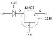
도 11의 스위칭 구조를 이용하면, 일반적인 CMOS기반의 스위치를 이용하는 경우와 다르게, 큰 값의 V+ 및 V- 전원 없이, 작은 제어 신호의 전압으로 스위치를 턴 오프 시킬 수 있다.Using the switching structure of FIG. 11, the switch can be turned off with a voltage of a small control signal, without using a large value of V + and V-power, unlike the case of using a general CMOS-based switch.
도 11을 참조하면, 일실시예에 따른 스위칭 구조는 다이오드(1110) 및 NMOS(1120)를 포함한다. NMOS(1120)의 게이트단(G)에 드레인단(D) 또는 소스단(S)보다 문턱 전압 이상의 전압이 인가되지 않으면 NMOS(1120)는 턴 오프 상태를 유지할 수 있다. 다이오드(1110)는 교류 전류 신호의 마이너스 성분의 유입을 차단할 수 있다. 교류 전류 신호의 플러스 성분의 유입은 NMOS(1120)에 의해 차단될 수 있다.Referring to FIG. 11, the switching structure according to an embodiment includes a
도 11의 예에서는 다이오드(1110)가 NMOS(1120)의 드레인단(D)에 연결되어 있으나, 다른 예로 다이오드(1110)는 NMOS(1120)의 소스단(S)에 연결될 수도 있다. 또한, 도 11의 스위칭 구조는 무선으로 전력을 수신하는 RX단 뿐만 아니라, 무선으로 전력을 전송하는 TX단에도 사용될 수 있다.11, the
NMOS(1120)의 게이트단(G)에 드레인단(D) 또는 소스단(S)보다 문턱 전압 이상의 전압이 인가되면 NMOS(1120)는 턴 온 상태를 유지할 수 있다. 다이오드(1110)는 직류 신호를 통과시키고, 역방향의 교류 전류 신호를 차단할 수 있다. 또한, 다이오드(1110)는 순방향의 교류 전류 신호의 플러스 성분을 통과시켜 정류기능을 수행할 수 있다.The
따라서, 일실시예에 따른 스위칭 구조를 이용하는 경우, 상대적으로 낮은 구동전압을 가지는 제어 신호를 통해서, 큰 진폭의 신호를 통과시키고 또한, 유입을 차단할 수 있다.
Therefore, when the switching structure according to one embodiment is used, a large amplitude signal can be passed through the control signal having a relatively low driving voltage, and the flow can be blocked.
도 12는 일실시예에 따른 무선 전력 수신 장치에 사용되는 스위칭 구조(1210)를 나타낸 도면이다.12 is a diagram illustrating a
도 12는 도 11의 스위칭 구조(1210)를 무선 전력 수신 장치에 적용한 회로도 를 나타낸다. 만약 0V의 VIN 이 NMOS의 게이트단에 인가된다고 가정하면, 상호 공진을 통해 타겟 공진기에 큰 진폭을 가지는 전압이 유기되는 경우에도 NMOS는 턴 오프 상태를 유지할 수 있다.Fig. 12 shows a circuit diagram in which the
또한, 타겟 공진기에 유기된 교류 신호의 피크 전압 보다 문턱 전압 이상의 전압이 게이트단에 인가되면 NMOS는 턴 온 상태를 유지할 수 있다.Further, when a voltage higher than the threshold voltage of the AC signal induced in the target resonator is applied to the gate terminal, the NMOS can maintain the turn-on state.
이때, 다이오드 전단의 타겟 공진기에서 발생하는 교류 전류 신호는 다이오드에 순방향 바이어스가 인가되는 경우에만 정류되어 직류 신호로 통과될 수 있다. 도 9 및 도 11에서 MOS 트랜지스터를 이용한 예를 개시하였으나, BJT등 다른 종류의 트랜지스터를 이용해서도 스위칭 구조의 구현이 가능하다.
At this time, the alternating current signal generated in the target resonator in the front end of the diode can be rectified only when the forward bias is applied to the diode, and can be passed as the direct current signal. Although an example using MOS transistors is shown in Figs. 9 and 11, it is possible to implement a switching structure using other types of transistors such as a BJT.
도 13은 일실시예에 따른 무선 전력 전송 방법의 흐름도이다.13 is a flowchart of a wireless power transmission method according to an embodiment.
1310단계에서, 일실시예에 따른 무선 전력 전송 장치는 트랜지스터에 의하여 트랜지스터의 제어 신호의 값과 기준 값을 비교한 결과에 기초하여 전원 공급부와 소스 공진기의 연결을 턴 온(turn on) 또는 턴 오프(turn off)할 수 있다.In
1320단계에서, 일실시예에 따른 무선 전력 전송 장치는 트랜지스터 및 트랜지스터와 직렬로 연결된 다이오드에 의하여, 트랜지스터의 턴 온 상태에서 전원 공급부의 직류 신호를 통과시키고, 트랜지스터의 턴 오프 상태에서 소스 공진기로부터 교류 신호의 유입을 차단할 수 있다.In
일실시예에 따른 무선 전력 전송 장치는 턴 오프의 상태가 유지되는 동안 다이오드에 의하여 소스 공진기에서 발생하는 교류 전류 신호의 플러스 성분의 유입을 차단하고, 트랜지스터에 의하여 교류 전류 신호의 마이너스 성분의 유입을 차단할 수 있다.The wireless power transmission apparatus according to an exemplary embodiment of the present invention can prevent a positive component of an alternating current signal generated in a source resonator by a diode from being inputted while a turn-off state is maintained and prevent a negative component of an alternating current signal from flowing Can be blocked.
1330단계에서, 일실시예에 따른 무선 전력 전송 장치는 턴 온 상태에서 전원 공급부로부터 소스 공진기로 전력을 공급할 수 있다.In
1340단계에서, 일실시예에 따른 무선 전력 전송 장치는 타겟 공진기와의 상호 공진을 통하여 소스 공진기로부터 전력을 전송할 수 있다.In
일실시예에 따른 무선 전력 전송 장치는 제어 신호를 생성하고, 소스 공진기로 공급하려는 전력량에 기초하여 제어 신호의 진폭 및 주기 중 적어도 하나를 제어할 수 있다.A wireless power transmission apparatus according to an embodiment can generate a control signal and control at least one of the amplitude and the period of the control signal based on the amount of power to supply to the source resonator.
일 실시예에 따른 무선 전력 전송 장치는 트랜지스터와 다이오드를 포함하는 스위칭 구조를 이용함으로써, 낮은 구동 전압으로 스위치를 동작시킬 수 있고, 많은 전류를 소스 공진기로 공급할 수 있을 뿐만 아니라, 소스 공진기에서 발생하는 큰 진폭을 가지는 교류 전류 신호의 트랜지스터로의 유입을 차단할 수 있다.A wireless power transmission apparatus according to an embodiment uses a switching structure including a transistor and a diode to operate the switch with a low driving voltage and not only can supply a large amount of current to the source resonator, The flow of the AC current signal having a large amplitude to the transistor can be blocked.
일 실시예에 따른 무선 전력 전송 장치는 트랜지스터와 다이오드를 포함하는 스위칭 구조를 이용함으로써, 낮은 구동 전압으로 스위치를 동작시켜, 낮은 전압뿐만 아니라 높은 전압의 신호를 통과 혹은 차단시킬 수 있다.A wireless power transmission apparatus according to an embodiment uses a switching structure including a transistor and a diode to operate a switch with a low driving voltage so as to pass or block a signal of a high voltage as well as a low voltage.
일 실시예에 따른 트랜지스터와 다이오드를 포함하는 스위칭 구조는 상호 공진을 이용한 에너지 및 데이터 동시 전송 시스템뿐만 아니라, 아날로그 신호의 스위칭이 필요한 어떠한 구조에도 적용될 수 있다.The switching structure including the transistor and the diode according to an embodiment can be applied to any structure that requires switching of an analog signal as well as a simultaneous energy and data transmission system using mutual resonance.
일 실시예에 따른 무선 전력 전송 장치는 트랜지스터와 다이오드를 포함하는 스위칭 구조를 이용함으로써, 단일 극성의 전원으로도 스위치를 구동시킬 수 있다.A wireless power transmission apparatus according to an embodiment can use a switching structure including a transistor and a diode to drive a switch with a single polarity power supply.
실시예에 따른 방법은 다양한 컴퓨터 수단을 통하여 실행될 수 있는 프로그램 명령 형태로 구현되어 컴퓨터 판독 가능 매체에 기록될 수 있다. 상기 컴퓨터 판독 가능 매체는 프로그램 명령, 데이터 파일, 데이터 구조 등을 단독으로 또는 조합하여 포함할 수 있다. 상기 매체에 기록되는 프로그램 명령은 실시예를 위하여 특별히 설계되고 구성된 것들이거나 컴퓨터 소프트웨어 당업자에게 공지되어 사용 가능한 것일 수도 있다. 컴퓨터 판독 가능 기록 매체의 예에는 하드 디스크, 플로피 디스크 및 자기 테이프와 같은 자기 매체(magnetic media), CD-ROM, DVD와 같은 광기록 매체(optical media), 플롭티컬 디스크(floptical disk)와 같은 자기-광 매체(magneto-optical media), 및 롬(ROM), 램(RAM), 플래시 메모리 등과 같은 프로그램 명령을 저장하고 실행하도록 특별히 구성된 하드웨어 장치가 포함된다. 프로그램 명령의 예에는 컴파일러에 의해 만들어지는 것과 같은 기계어 코드뿐만 아니라 인터프리터 등을 사용해서 컴퓨터에 의해서 실행될 수 있는 고급 언어 코드를 포함한다. 상기된 하드웨어 장치는 실시예의 동작을 수행하기 위해 하나 이상의 소프트웨어 모듈로서 작동하도록 구성될 수 있으며, 그 역도 마찬가지이다.The method according to an embodiment may be implemented in the form of program instructions that can be executed through various computer means and recorded on a computer readable medium. The computer-readable medium may include program instructions, data files, data structures, and the like, alone or in combination. The program instructions to be recorded on the medium may be those specially designed and configured for the embodiments or may be available to those skilled in the art of computer software. Examples of computer-readable media include magnetic media such as hard disks, floppy disks, and magnetic tape; optical media such as CD-ROMs and DVDs; magnetic media such as floppy disks; Magneto-optical media, and hardware devices specifically configured to store and execute program instructions, such as ROM, RAM, flash memory, and the like. Examples of program instructions include machine language code such as those produced by a compiler, as well as high-level language code that can be executed by a computer using an interpreter or the like. The hardware devices described above may be configured to operate as one or more software modules to perform the operations of the embodiments, and vice versa.
이상과 같이 실시예들이 비록 한정된 실시예와 도면에 의해 설명되었으나, 해당 기술분야에서 통상의 지식을 가진 자라면 상기의 기재로부터 다양한 수정 및 변형이 가능하다. 예를 들어, 설명된 기술들이 설명된 방법과 다른 순서로 수행되거나, 및/또는 설명된 시스템, 구조, 장치, 회로 등의 구성요소들이 설명된 방법과 다른 형태로 결합 또는 조합되거나, 다른 구성요소 또는 균등물에 의하여 대치되거나 치환되더라도 적절한 결과가 달성될 수 있다.While the present invention has been particularly shown and described with reference to exemplary embodiments thereof, it is to be understood that the invention is not limited to the disclosed exemplary embodiments. For example, it is to be understood that the techniques described may be performed in a different order than the described methods, and / or that components of the described systems, structures, devices, circuits, Lt; / RTI > or equivalents, even if it is replaced or replaced.
그러므로, 다른 구현들, 다른 실시예들 및 특허청구범위와 균등한 것들도 후술하는 특허청구범위의 범위에 속한다.Therefore, other implementations, other embodiments, and equivalents to the claims are also within the scope of the following claims.
Claims (16)
Translated fromKorean상기 소스 공진기로 전력을 공급하는 전원 공급부;
제어 신호를 생성하고, 상기 제어 신호의 진폭을 상기 소스 공진기로 공급할 전력량에 기초하여 제어하거나 또는 상기 제어 신호의 주파수를 상기 소스 공진기로 공급할 전력량에 기초하여 제어하는 제어부; 및
상기 제어 신호에 기초하여 상기 전원 공급부와 상기 소스 공진기를 연결하는 스위칭부를 포함하고,
상기 스위칭부는
상기 제어 신호의 값과 기준 값을 비교한 결과에 기초하여 상기 전원 공급부와 상기 소스 공진기의 연결을 턴 온(turn on) 또는 턴 오프(turn off)하는 트랜지스터; 및
상기 트랜지스터와 직렬로 연결된 다이오드
를 포함하는 무선 전력 전송 장치.A source resonator for transmitting power through mutual resonance with the target resonator;
A power supply for supplying power to the source resonator;
A control unit for generating a control signal and controlling the amplitude of the control signal based on an amount of power to be supplied to the source resonator or based on an amount of power to be supplied to the source resonator; And
And a switching unit for connecting the power supply unit and the source resonator based on the control signal,
The switching unit
A transistor for turning on or off a connection between the power supply unit and the source resonator based on a result of comparing the value of the control signal with a reference value; And
A diode coupled in series with the transistor
And a wireless power transmission device.
상기 턴 온의 상태가 유지되는 동안 상기 다이오드 및 상기 트랜지스터는 상기 전원 공급부로부터 공급하는 직류 전류 신호를 통과시키고,
상기 턴 오프의 상태가 유지되는 동안 상기 다이오드는 상기 소스 공진기에서 발생하는 교류 전류 신호의 플러스 성분의 유입을 차단하고, 상기 트랜지스터는 상기 교류 전류 신호의 마이너스 성분의 유입을 차단하는
무선 전력 전송 장치.The method according to claim 1,
Wherein the diode and the transistor pass the direct current signal supplied from the power supply while the turn-on state is maintained,
The diode interrupts the inflow of the positive component of the alternating current signal generated in the source resonator while the turnoff state is maintained and the transistor interrupts the inflow of the negative component of the alternating current signal
Wireless power transmission device.
상기 소스 공진기로 전력을 공급하는 전원 공급부; 및
제어 신호에 기초하여 상기 전원 공급부와 상기 소스 공진기를 연결하는 스위칭부를 포함하고,
상기 스위칭부는,
상기 제어 신호의 값과 기준 값을 비교한 결과에 기초하여 상기 전원 공급부와 상기 소스 공진기의 연결을 턴 온(turn on) 또는 턴 오프(turn off)하는 트랜지스터; 및
상기 트랜지스터와 직렬로 연결된 다이오드를 포함하고,
상기 트랜지스터가 피모스(PMOS, P-channel Metal Oxide Semiconductor)인 경우, 상기 제어 신호는 상기 피모스의 게이트에 인가되고,
상기 제어 신호의 전압이 상기 피모스의 소스에 인가되는 전압과 상기 피모스의 문턱전압의 차이보다 작거나 같으면, 상기 전원 공급부와 상기 소스 공진기의 연결을 턴 온(turn on)시키고,
상기 제어 신호의 전압이 상기 피모스의 소스에 인가되는 전압과 상기 피모스의 문턱전압의 차이보다 커지면, 상기 전원 공급부와 상기 소스 공진기의 연결을 턴 오프(turn off)시키는
무선 전력 전송 장치.A source resonator for transmitting power through mutual resonance with the target resonator;
A power supply for supplying power to the source resonator; And
And a switching unit connecting the power supply unit and the source resonator based on a control signal,
The switching unit includes:
A transistor for turning on or off a connection between the power supply unit and the source resonator based on a result of comparing the value of the control signal with a reference value; And
A diode coupled in series with the transistor,
When the transistor is a PMOS (P-channel Metal Oxide Semiconductor), the control signal is applied to the gate of the PMOS transistor,
And turning on the connection between the power supply and the source resonator if the voltage of the control signal is less than or equal to a difference between a voltage applied to the source of the emitter and a threshold voltage of the emitter,
And turning off the connection between the power supply and the source resonator when the voltage of the control signal is greater than the difference between the voltage applied to the source of the emitter and the threshold voltage of the emitter
Wireless power transmission device.
상기 다이오드는 상기 피모스와 직렬로 연결되고,
상기 다이오드 및 상기 피모스는
상기 턴 온의 상태가 유지되는 동안 상기 전원 공급부로부터 공급하는 직류 전류 신호를 통과시키고,
상기 턴 오프의 상태가 유지되는 동안 상기 소스 공진기로부터 교류 전류 신호의 유입을 차단하는
무선 전력 전송 장치.5. The method of claim 4,
Said diode being connected in series with said picture,
The diode and the PMOS
A DC current signal supplied from the power supply unit while the turn-on state is maintained,
While the state of the turn-off is maintained, the flow of the AC current signal from the source resonator is blocked
Wireless power transmission device.
상기 소스 공진기로 전력을 공급하는 전원 공급부; 및
제어 신호에 기초하여 상기 전원 공급부와 상기 소스 공진기를 연결하는 스위칭부를 포함하고,
상기 스위칭부는,
상기 제어 신호의 값과 기준 값을 비교한 결과에 기초하여 상기 전원 공급부와 상기 소스 공진기의 연결을 턴 온(turn on) 또는 턴 오프(turn off)하는 트랜지스터; 및
상기 트랜지스터와 직렬로 연결된 다이오드를 포함하고,
상기 트랜지스터가 엔모스(NMOS, N-channel Metal Oxide Semiconductor)인 경우, 상기 제어 신호는 상기 엔모스의 게이트에 인가되고,
상기 제어 신호의 전압이 상기 엔모스의 소스에 인가되는 전압과 상기 엔모스의 문턱전압의 합보다 크거나 같으면, 상기 전원 공급부와 상기 소스 공진기의 연결을 턴 온(turn on)시키고,
상기 제어 신호의 전압이 상기 엔모스의 소스에 인가되는 전압과 상기 엔모스의 문턱전압의 합보다 작아지면, 상기 전원 공급부와 상기 소스 공진기의 연결을 턴 오프(turn off)시키는
무선 전력 전송 장치.A source resonator for transmitting power through mutual resonance with the target resonator;
A power supply for supplying power to the source resonator; And
And a switching unit connecting the power supply unit and the source resonator based on a control signal,
The switching unit includes:
A transistor for turning on or off a connection between the power supply unit and the source resonator based on a result of comparing the value of the control signal with a reference value; And
A diode coupled in series with the transistor,
When the transistor is an NMOS (N-channel Metal Oxide Semiconductor), the control signal is applied to the gate of the NMOS transistor,
And turning on the connection between the power supply and the source resonator if the voltage of the control signal is greater than or equal to the sum of the voltage applied to the source of the emmos and the threshold voltage of the emmos,
And turning off the connection between the power supply and the source resonator when the voltage of the control signal becomes less than the sum of the voltage applied to the source of the emmos and the threshold voltage of the emmos
Wireless power transmission device.
상기 다이오드는 상기 엔모스와 직렬로 연결되고,
상기 다이오드 및 상기 엔모스는
상기 턴 온의 상태가 유지되는 동안 상기 전원 공급부로부터 공급하는 직류 전류 신호를 통과시키고,
상기 턴 오프의 상태가 유지되는 동안 상기 소스 공진기로부터 교류 전류 신호의 유입을 차단하는
무선 전력 전송 장치.The method according to claim 6,
The diode being connected in series with the emmos,
The diode and the NMOS
A DC current signal supplied from the power supply unit while the turn-on state is maintained,
While the state of the turn-off is maintained, the flow of the AC current signal from the source resonator is blocked
Wireless power transmission device.
상기 트랜지스터가 바이폴라 접합 트랜지스터(BJT, Bipolar Junction Transistor)인 경우, 상기 트랜지스터는 상기 바이폴라 접합 트랜지스터의 베이스(Base)에 인가되는 상기 제어 신호의 전류 값에 기초하여 상기 전원 공급부와 상기 소스 공진기의 연결을 턴 온(turn on) 또는 턴 오프(turn off)하는
무선 전력 전송 장치.The method according to claim 1,
When the transistor is a bipolar junction transistor (BJT), the transistor is connected to the base of the bipolar junction transistor based on a current value of the control signal, Turn-on or turn-off
Wireless power transmission device.
상기 다이오드는 상기 바이폴라 접합 트랜지스터와 직렬로 연결되고,
상기 다이오드 및 상기 바이폴라 접합 트랜지스터는
상기 턴 온의 상태가 유지되는 동안 상기 전원 공급부로부터 공급하는 직류 전류 신호를 통과시키고,
상기 턴 오프의 상태가 유지되는 동안 상기 소스 공진기로부터 교류 전류 신호의 유입을 차단하는
무선 전력 전송 장치.9. The method of claim 8,
The diode being connected in series with the bipolar junction transistor,
The diode and the bipolar junction transistor
A DC current signal supplied from the power supply unit while the turn-on state is maintained,
While the state of the turn-off is maintained, the flow of the AC current signal from the source resonator is blocked
Wireless power transmission device.
상기 전원 공급부와 상기 스위칭부 사이에 위치하는 가변저항
을 더 포함하는 무선 전력 전송 장치.The method according to claim 1,
A variable resistor located between the power supply unit and the switching unit;
Lt; / RTI >
상기 전원 공급부와 병렬로 연결되는 복수개의 저항들; 및
상기 복수개의 저항들 각각과 직렬로 연결되는 스위치들
을 더 포함하는 무선 전력 전송 장치.The method according to claim 1,
A plurality of resistors connected in parallel with the power supply; And
Switches connected in series with each of the plurality of resistors
Lt; / RTI >
상기 트랜지스터 및 상기 트랜지스터와 직렬로 연결된 다이오드에 의하여, 상기 트랜지스터의 턴 온 상태에서 상기 전원 공급부의 직류 신호를 통과시키고, 상기 트랜지스터의 턴 오프 상태에서 상기 소스 공진기로부터 교류 신호의 유입을 차단하는 단계;
상기 턴 온 상태에서 상기 전원 공급부로부터 상기 소스 공진기로 전력을 공급하는 단계;
타겟 공진기와의 상호 공진을 통하여 상기 소스 공진기로부터 전력을 전송하는 단계;
상기 제어 신호를 생성하는 단계; 및
상기 제어 신호의 진폭을 상기 소스 공진기로 공급할 전력량에 기초하여 제어하거나 또는 상기 제어 신호의 주파수를 상기 소스 공진기로 공급할 전력량에 기초하여 제어하는 단계
를 포함하는 무선 전력 전송 방법.Turning on or off the connection between the power supply and the source resonator based on a result of comparing the value of the control signal of the transistor with a reference value by the transistor;
Passing a direct current signal of the power supply in a turned-on state of the transistor by a diode connected in series with the transistor and the transistor, and blocking the flow of an AC signal from the source resonator in a turned off state of the transistor;
Supplying power from the power supply to the source resonator in the turn-on state;
Transmitting power from the source resonator through mutual resonance with the target resonator;
Generating the control signal; And
Controlling the amplitude of the control signal based on an amount of power to be supplied to the source resonator or controlling based on an amount of power to be supplied to the source resonator
/ RTI >
상기 차단하는 단계는
상기 턴 오프의 상태가 유지되는 동안 상기 다이오드에 의하여 상기 소스 공진기에서 발생하는 교류 전류 신호의 플러스 성분의 유입을 차단하고, 상기 트랜지스터에 의하여 상기 교류 전류 신호의 마이너스 성분의 유입을 차단하는
무선 전력 전송 방법.15. The method of claim 14,
The blocking step
Off state of the AC current signal generated in the source resonator by the diode while the state of the turn-off state is maintained, and the negative component of the AC current signal is blocked by the transistor
Wireless power transmission method.
Priority Applications (2)
| Application Number | Priority Date | Filing Date | Title |
|---|---|---|---|
| KR1020120121980AKR101902228B1 (en) | 2012-10-31 | 2012-10-31 | Wireless power transmission apparatus and method thereof |
| US14/065,916US9601948B2 (en) | 2012-10-31 | 2013-10-29 | Wireless power transmission apparatus and method |
Applications Claiming Priority (1)
| Application Number | Priority Date | Filing Date | Title |
|---|---|---|---|
| KR1020120121980AKR101902228B1 (en) | 2012-10-31 | 2012-10-31 | Wireless power transmission apparatus and method thereof |
Publications (2)
| Publication Number | Publication Date |
|---|---|
| KR20140055325A KR20140055325A (en) | 2014-05-09 |
| KR101902228B1true KR101902228B1 (en) | 2018-09-28 |
Family
ID=50546377
Family Applications (1)
| Application Number | Title | Priority Date | Filing Date |
|---|---|---|---|
| KR1020120121980AActiveKR101902228B1 (en) | 2012-10-31 | 2012-10-31 | Wireless power transmission apparatus and method thereof |
Country Status (2)
| Country | Link |
|---|---|
| US (1) | US9601948B2 (en) |
| KR (1) | KR101902228B1 (en) |
Families Citing this family (7)
| Publication number | Priority date | Publication date | Assignee | Title |
|---|---|---|---|---|
| US20150091523A1 (en)* | 2013-10-02 | 2015-04-02 | Mediatek Singapore Pte. Ltd. | Wireless charger system that has variable power / adaptive load modulation |
| US9559605B2 (en)* | 2014-03-05 | 2017-01-31 | Ricoh Co., Ltd. | System for ambient energy harvesting |
| US10468917B2 (en) | 2014-03-05 | 2019-11-05 | Ricoh Co., Ltd. | Battery charger |
| US10298071B2 (en) | 2014-03-05 | 2019-05-21 | Ricoh Co., Ltd | DC-DC boost converter |
| US9641364B2 (en)* | 2014-05-30 | 2017-05-02 | Nxp B.V. | Communication circuit and approach with modulation |
| CN111953082B (en)* | 2019-05-14 | 2023-12-22 | 伏达半导体(合肥)股份有限公司 | Efficient wireless charging system and method |
| JP6849778B1 (en)* | 2019-12-05 | 2021-03-31 | パナソニック株式会社 | Wireless transmitter and wireless receiver |
Citations (1)
| Publication number | Priority date | Publication date | Assignee | Title |
|---|---|---|---|---|
| US20090096413A1 (en)* | 2006-01-31 | 2009-04-16 | Mojo Mobility, Inc. | System and method for inductive charging of portable devices |
Family Cites Families (7)
| Publication number | Priority date | Publication date | Assignee | Title |
|---|---|---|---|---|
| JP2998768B2 (en) | 1992-01-27 | 2000-01-11 | 日本電信電話株式会社 | MOSFET drive circuit |
| US6509781B2 (en) | 2001-03-20 | 2003-01-21 | Koninklijke Philips Electronics N.V. | Circuit and method for controlling a dynamic, bi-directional high voltage analog switch |
| US6700433B2 (en) | 2002-03-11 | 2004-03-02 | Fairchild Semiconductor Corporation | Drain activated/deactivated AC coupled bandpass RF switch |
| CA2471393A1 (en) | 2003-06-18 | 2004-12-18 | Marlex Engineering Inc. | Low voltage low loss piezoelectric driver and switching apparatus |
| US7376212B2 (en) | 2004-06-03 | 2008-05-20 | Silicon Laboratories Inc. | RF isolator with differential input/output |
| US7352084B2 (en)* | 2004-08-11 | 2008-04-01 | Sensormatic Electronics Corporation | Deactivator using inductive charging |
| US9118322B2 (en) | 2010-10-12 | 2015-08-25 | Alpha And Omega Semiconductor (Cayman) Ltd | Low leakage dynamic bi-directional body-snatching (LLDBBS) scheme for high speed analog switches |
- 2012
- 2012-10-31KRKR1020120121980Apatent/KR101902228B1/enactiveActive
- 2013
- 2013-10-29USUS14/065,916patent/US9601948B2/enactiveActive
Patent Citations (1)
| Publication number | Priority date | Publication date | Assignee | Title |
|---|---|---|---|---|
| US20090096413A1 (en)* | 2006-01-31 | 2009-04-16 | Mojo Mobility, Inc. | System and method for inductive charging of portable devices |
Also Published As
| Publication number | Publication date |
|---|---|
| US9601948B2 (en) | 2017-03-21 |
| US20140117771A1 (en) | 2014-05-01 |
| KR20140055325A (en) | 2014-05-09 |
Similar Documents
| Publication | Publication Date | Title |
|---|---|---|
| KR101949954B1 (en) | Wireless power transmission apparatus for high efficient energy charging | |
| KR101902228B1 (en) | Wireless power transmission apparatus and method thereof | |
| CN109742824B (en) | Charging systems and electronics | |
| US10714979B2 (en) | Wireless power receiving terminal and wireless charging system | |
| CN105379137B (en) | Wireless Power Receiver with Programmable Power Path | |
| JP6062556B2 (en) | Feedback control coil driver for inductive power transfer | |
| KR101730406B1 (en) | Apparatus for wireless power transmission and reception | |
| KR101931256B1 (en) | Wireless power reception apparatus and method | |
| KR101987315B1 (en) | Wireless power transfer device and energy charging device | |
| Chan et al. | A primary side control method for wireless energy transmission system | |
| JP6207045B2 (en) | Wireless inductive power transmission | |
| US10164475B2 (en) | Wireless power receiver | |
| US20140177305A1 (en) | Gate drive circuit for synchronous rectification | |
| EP2985846A1 (en) | Wireless power transmission | |
| CN103580490A (en) | Dc-dc converter | |
| Shin et al. | A time-interleaved resonant voltage mode wireless power receiver with delay-based tracking loops for implantable medical devices | |
| US9882493B2 (en) | Apparatus and method for isolated current mode controller | |
| KR20160012020A (en) | Wireless power transfer system and method based on transfer schedule | |
| KR101949127B1 (en) | Method and apparatus for wireless energy transmission with hybrid synchronization scheme | |
| US20170244254A1 (en) | Devices, systems, and methods for adjusting output power using synchronous rectifier control | |
| KR20140004870A (en) | Data reception apparatus and method thereof, data transmission apparatus, data communication system | |
| KR102773408B1 (en) | Wireless power transfer power control techniques | |
| JP7185676B2 (en) | Semiconductor relay device | |
| Jiang et al. | A feed-forward controlled ac-dc boost converter for biomedical implants | |
| Jiang et al. | A low-input-voltage wireless power transfer for biomedical implants |
Legal Events
| Date | Code | Title | Description |
|---|---|---|---|
| PA0109 | Patent application | St.27 status event code:A-0-1-A10-A12-nap-PA0109 | |
| PN2301 | Change of applicant | St.27 status event code:A-3-3-R10-R13-asn-PN2301 St.27 status event code:A-3-3-R10-R11-asn-PN2301 | |
| PG1501 | Laying open of application | St.27 status event code:A-1-1-Q10-Q12-nap-PG1501 | |
| A201 | Request for examination | ||
| PA0201 | Request for examination | St.27 status event code:A-1-2-D10-D11-exm-PA0201 | |
| D13-X000 | Search requested | St.27 status event code:A-1-2-D10-D13-srh-X000 | |
| D14-X000 | Search report completed | St.27 status event code:A-1-2-D10-D14-srh-X000 | |
| E902 | Notification of reason for refusal | ||
| PE0902 | Notice of grounds for rejection | St.27 status event code:A-1-2-D10-D21-exm-PE0902 | |
| E13-X000 | Pre-grant limitation requested | St.27 status event code:A-2-3-E10-E13-lim-X000 | |
| P11-X000 | Amendment of application requested | St.27 status event code:A-2-2-P10-P11-nap-X000 | |
| P13-X000 | Application amended | St.27 status event code:A-2-2-P10-P13-nap-X000 | |
| E90F | Notification of reason for final refusal | ||
| PE0902 | Notice of grounds for rejection | St.27 status event code:A-1-2-D10-D21-exm-PE0902 | |
| P11-X000 | Amendment of application requested | St.27 status event code:A-2-2-P10-P11-nap-X000 | |
| P13-X000 | Application amended | St.27 status event code:A-2-2-P10-P13-nap-X000 | |
| E701 | Decision to grant or registration of patent right | ||
| PE0701 | Decision of registration | St.27 status event code:A-1-2-D10-D22-exm-PE0701 | |
| GRNT | Written decision to grant | ||
| PR0701 | Registration of establishment | St.27 status event code:A-2-4-F10-F11-exm-PR0701 | |
| PR1002 | Payment of registration fee | St.27 status event code:A-2-2-U10-U11-oth-PR1002 Fee payment year number:1 | |
| PG1601 | Publication of registration | St.27 status event code:A-4-4-Q10-Q13-nap-PG1601 | |
| P22-X000 | Classification modified | St.27 status event code:A-4-4-P10-P22-nap-X000 | |
| P22-X000 | Classification modified | St.27 status event code:A-4-4-P10-P22-nap-X000 | |
| R18-X000 | Changes to party contact information recorded | St.27 status event code:A-5-5-R10-R18-oth-X000 | |
| P22-X000 | Classification modified | St.27 status event code:A-4-4-P10-P22-nap-X000 | |
| PR1001 | Payment of annual fee | St.27 status event code:A-4-4-U10-U11-oth-PR1001 Fee payment year number:4 | |
| PR1001 | Payment of annual fee | St.27 status event code:A-4-4-U10-U11-oth-PR1001 Fee payment year number:5 | |
| PR1001 | Payment of annual fee | St.27 status event code:A-4-4-U10-U11-oth-PR1001 Fee payment year number:6 | |
| P22-X000 | Classification modified | St.27 status event code:A-4-4-P10-P22-nap-X000 | |
| R18-X000 | Changes to party contact information recorded | St.27 status event code:A-5-5-R10-R18-oth-X000 | |
| PR1001 | Payment of annual fee | St.27 status event code:A-4-4-U10-U11-oth-PR1001 Fee payment year number:7 | |
| PR1001 | Payment of annual fee | St.27 status event code:A-4-4-U10-U11-oth-PR1001 Fee payment year number:8 |