KR101901712B1 - Fan-out semiconductor package - Google Patents
Fan-out semiconductor packageDownload PDFInfo
- Publication number
- KR101901712B1 KR101901712B1KR1020170141138AKR20170141138AKR101901712B1KR 101901712 B1KR101901712 B1KR 101901712B1KR 1020170141138 AKR1020170141138 AKR 1020170141138AKR 20170141138 AKR20170141138 AKR 20170141138AKR 101901712 B1KR101901712 B1KR 101901712B1
- Authority
- KR
- South Korea
- Prior art keywords
- layer
- fan
- semiconductor package
- layers
- semiconductor chip
- Prior art date
- Legal status (The legal status is an assumption and is not a legal conclusion. Google has not performed a legal analysis and makes no representation as to the accuracy of the status listed.)
- Active
Links
Images


Classifications
- H—ELECTRICITY
- H01—ELECTRIC ELEMENTS
- H01L—SEMICONDUCTOR DEVICES NOT COVERED BY CLASS H10
- H01L25/00—Assemblies consisting of a plurality of semiconductor or other solid state devices
- H01L25/03—Assemblies consisting of a plurality of semiconductor or other solid state devices all the devices being of a type provided for in a single subclass of subclasses H10B, H10D, H10F, H10H, H10K or H10N, e.g. assemblies of rectifier diodes
- H01L25/04—Assemblies consisting of a plurality of semiconductor or other solid state devices all the devices being of a type provided for in a single subclass of subclasses H10B, H10D, H10F, H10H, H10K or H10N, e.g. assemblies of rectifier diodes the devices not having separate containers
- H01L25/07—Assemblies consisting of a plurality of semiconductor or other solid state devices all the devices being of a type provided for in a single subclass of subclasses H10B, H10D, H10F, H10H, H10K or H10N, e.g. assemblies of rectifier diodes the devices not having separate containers the devices being of a type provided for in group subclass H10D
- H01L25/073—Apertured devices mounted on one or more rods passed through the apertures
- H—ELECTRICITY
- H01—ELECTRIC ELEMENTS
- H01L—SEMICONDUCTOR DEVICES NOT COVERED BY CLASS H10
- H01L23/00—Details of semiconductor or other solid state devices
- H01L23/52—Arrangements for conducting electric current within the device in operation from one component to another, i.e. interconnections, e.g. wires, lead frames
- H01L23/538—Arrangements for conducting electric current within the device in operation from one component to another, i.e. interconnections, e.g. wires, lead frames the interconnection structure between a plurality of semiconductor chips being formed on, or in, insulating substrates
- H01L23/5389—Arrangements for conducting electric current within the device in operation from one component to another, i.e. interconnections, e.g. wires, lead frames the interconnection structure between a plurality of semiconductor chips being formed on, or in, insulating substrates the chips being integrally enclosed by the interconnect and support structures
- H—ELECTRICITY
- H01—ELECTRIC ELEMENTS
- H01L—SEMICONDUCTOR DEVICES NOT COVERED BY CLASS H10
- H01L23/00—Details of semiconductor or other solid state devices
- H01L23/48—Arrangements for conducting electric current to or from the solid state body in operation, e.g. leads, terminal arrangements ; Selection of materials therefor
- H01L23/488—Arrangements for conducting electric current to or from the solid state body in operation, e.g. leads, terminal arrangements ; Selection of materials therefor consisting of soldered or bonded constructions
- H01L23/498—Leads, i.e. metallisations or lead-frames on insulating substrates, e.g. chip carriers
- H01L23/49822—Multilayer substrates
- H—ELECTRICITY
- H01—ELECTRIC ELEMENTS
- H01L—SEMICONDUCTOR DEVICES NOT COVERED BY CLASS H10
- H01L23/00—Details of semiconductor or other solid state devices
- H01L23/28—Encapsulations, e.g. encapsulating layers, coatings, e.g. for protection
- H—ELECTRICITY
- H01—ELECTRIC ELEMENTS
- H01L—SEMICONDUCTOR DEVICES NOT COVERED BY CLASS H10
- H01L23/00—Details of semiconductor or other solid state devices
- H01L23/28—Encapsulations, e.g. encapsulating layers, coatings, e.g. for protection
- H01L23/31—Encapsulations, e.g. encapsulating layers, coatings, e.g. for protection characterised by the arrangement or shape
- H01L23/3157—Partial encapsulation or coating
- H01L23/3171—Partial encapsulation or coating the coating being directly applied to the semiconductor body, e.g. passivation layer
- H—ELECTRICITY
- H01—ELECTRIC ELEMENTS
- H01L—SEMICONDUCTOR DEVICES NOT COVERED BY CLASS H10
- H01L23/00—Details of semiconductor or other solid state devices
- H01L23/48—Arrangements for conducting electric current to or from the solid state body in operation, e.g. leads, terminal arrangements ; Selection of materials therefor
- H01L23/482—Arrangements for conducting electric current to or from the solid state body in operation, e.g. leads, terminal arrangements ; Selection of materials therefor consisting of lead-in layers inseparably applied to the semiconductor body (electrodes)
- H01L23/485—Arrangements for conducting electric current to or from the solid state body in operation, e.g. leads, terminal arrangements ; Selection of materials therefor consisting of lead-in layers inseparably applied to the semiconductor body (electrodes) consisting of layered constructions comprising conductive layers and insulating layers, e.g. planar contacts
- H—ELECTRICITY
- H01—ELECTRIC ELEMENTS
- H01L—SEMICONDUCTOR DEVICES NOT COVERED BY CLASS H10
- H01L23/00—Details of semiconductor or other solid state devices
- H01L23/48—Arrangements for conducting electric current to or from the solid state body in operation, e.g. leads, terminal arrangements ; Selection of materials therefor
- H01L23/488—Arrangements for conducting electric current to or from the solid state body in operation, e.g. leads, terminal arrangements ; Selection of materials therefor consisting of soldered or bonded constructions
- H01L23/498—Leads, i.e. metallisations or lead-frames on insulating substrates, e.g. chip carriers
- H01L23/49811—Additional leads joined to the metallisation on the insulating substrate, e.g. pins, bumps, wires, flat leads
- H—ELECTRICITY
- H01—ELECTRIC ELEMENTS
- H01L—SEMICONDUCTOR DEVICES NOT COVERED BY CLASS H10
- H01L23/00—Details of semiconductor or other solid state devices
- H01L23/48—Arrangements for conducting electric current to or from the solid state body in operation, e.g. leads, terminal arrangements ; Selection of materials therefor
- H01L23/488—Arrangements for conducting electric current to or from the solid state body in operation, e.g. leads, terminal arrangements ; Selection of materials therefor consisting of soldered or bonded constructions
- H01L23/498—Leads, i.e. metallisations or lead-frames on insulating substrates, e.g. chip carriers
- H01L23/49827—Via connections through the substrates, e.g. pins going through the substrate, coaxial cables
- H—ELECTRICITY
- H01—ELECTRIC ELEMENTS
- H01L—SEMICONDUCTOR DEVICES NOT COVERED BY CLASS H10
- H01L23/00—Details of semiconductor or other solid state devices
- H01L23/52—Arrangements for conducting electric current within the device in operation from one component to another, i.e. interconnections, e.g. wires, lead frames
- H01L23/538—Arrangements for conducting electric current within the device in operation from one component to another, i.e. interconnections, e.g. wires, lead frames the interconnection structure between a plurality of semiconductor chips being formed on, or in, insulating substrates
- H—ELECTRICITY
- H01—ELECTRIC ELEMENTS
- H01L—SEMICONDUCTOR DEVICES NOT COVERED BY CLASS H10
- H01L24/00—Arrangements for connecting or disconnecting semiconductor or solid-state bodies; Methods or apparatus related thereto
- H01L24/01—Means for bonding being attached to, or being formed on, the surface to be connected, e.g. chip-to-package, die-attach, "first-level" interconnects; Manufacturing methods related thereto
- H01L24/02—Bonding areas ; Manufacturing methods related thereto
- H01L24/07—Structure, shape, material or disposition of the bonding areas after the connecting process
- H01L24/09—Structure, shape, material or disposition of the bonding areas after the connecting process of a plurality of bonding areas
- H—ELECTRICITY
- H01—ELECTRIC ELEMENTS
- H01L—SEMICONDUCTOR DEVICES NOT COVERED BY CLASS H10
- H01L24/00—Arrangements for connecting or disconnecting semiconductor or solid-state bodies; Methods or apparatus related thereto
- H01L24/01—Means for bonding being attached to, or being formed on, the surface to be connected, e.g. chip-to-package, die-attach, "first-level" interconnects; Manufacturing methods related thereto
- H01L24/18—High density interconnect [HDI] connectors; Manufacturing methods related thereto
- H01L24/19—Manufacturing methods of high density interconnect preforms
- H—ELECTRICITY
- H01—ELECTRIC ELEMENTS
- H01L—SEMICONDUCTOR DEVICES NOT COVERED BY CLASS H10
- H01L24/00—Arrangements for connecting or disconnecting semiconductor or solid-state bodies; Methods or apparatus related thereto
- H01L24/01—Means for bonding being attached to, or being formed on, the surface to be connected, e.g. chip-to-package, die-attach, "first-level" interconnects; Manufacturing methods related thereto
- H01L24/18—High density interconnect [HDI] connectors; Manufacturing methods related thereto
- H01L24/20—Structure, shape, material or disposition of high density interconnect preforms
- H—ELECTRICITY
- H01—ELECTRIC ELEMENTS
- H01L—SEMICONDUCTOR DEVICES NOT COVERED BY CLASS H10
- H01L24/00—Arrangements for connecting or disconnecting semiconductor or solid-state bodies; Methods or apparatus related thereto
- H01L24/01—Means for bonding being attached to, or being formed on, the surface to be connected, e.g. chip-to-package, die-attach, "first-level" interconnects; Manufacturing methods related thereto
- H01L24/26—Layer connectors, e.g. plate connectors, solder or adhesive layers; Manufacturing methods related thereto
- H01L24/31—Structure, shape, material or disposition of the layer connectors after the connecting process
- H01L24/32—Structure, shape, material or disposition of the layer connectors after the connecting process of an individual layer connector
- H—ELECTRICITY
- H01—ELECTRIC ELEMENTS
- H01L—SEMICONDUCTOR DEVICES NOT COVERED BY CLASS H10
- H01L2224/00—Indexing scheme for arrangements for connecting or disconnecting semiconductor or solid-state bodies and methods related thereto as covered by H01L24/00
- H01L2224/01—Means for bonding being attached to, or being formed on, the surface to be connected, e.g. chip-to-package, die-attach, "first-level" interconnects; Manufacturing methods related thereto
- H01L2224/02—Bonding areas; Manufacturing methods related thereto
- H01L2224/023—Redistribution layers [RDL] for bonding areas
- H01L2224/0237—Disposition of the redistribution layers
- H01L2224/02375—Top view
- H—ELECTRICITY
- H01—ELECTRIC ELEMENTS
- H01L—SEMICONDUCTOR DEVICES NOT COVERED BY CLASS H10
- H01L2224/00—Indexing scheme for arrangements for connecting or disconnecting semiconductor or solid-state bodies and methods related thereto as covered by H01L24/00
- H01L2224/01—Means for bonding being attached to, or being formed on, the surface to be connected, e.g. chip-to-package, die-attach, "first-level" interconnects; Manufacturing methods related thereto
- H01L2224/02—Bonding areas; Manufacturing methods related thereto
- H01L2224/023—Redistribution layers [RDL] for bonding areas
- H01L2224/0237—Disposition of the redistribution layers
- H01L2224/02377—Fan-in arrangement
- H—ELECTRICITY
- H01—ELECTRIC ELEMENTS
- H01L—SEMICONDUCTOR DEVICES NOT COVERED BY CLASS H10
- H01L2224/00—Indexing scheme for arrangements for connecting or disconnecting semiconductor or solid-state bodies and methods related thereto as covered by H01L24/00
- H01L2224/01—Means for bonding being attached to, or being formed on, the surface to be connected, e.g. chip-to-package, die-attach, "first-level" interconnects; Manufacturing methods related thereto
- H01L2224/02—Bonding areas; Manufacturing methods related thereto
- H01L2224/023—Redistribution layers [RDL] for bonding areas
- H01L2224/0237—Disposition of the redistribution layers
- H01L2224/02379—Fan-out arrangement
- H—ELECTRICITY
- H01—ELECTRIC ELEMENTS
- H01L—SEMICONDUCTOR DEVICES NOT COVERED BY CLASS H10
- H01L2224/00—Indexing scheme for arrangements for connecting or disconnecting semiconductor or solid-state bodies and methods related thereto as covered by H01L24/00
- H01L2224/01—Means for bonding being attached to, or being formed on, the surface to be connected, e.g. chip-to-package, die-attach, "first-level" interconnects; Manufacturing methods related thereto
- H01L2224/02—Bonding areas; Manufacturing methods related thereto
- H01L2224/04—Structure, shape, material or disposition of the bonding areas prior to the connecting process
- H01L2224/0401—Bonding areas specifically adapted for bump connectors, e.g. under bump metallisation [UBM]
- H—ELECTRICITY
- H01—ELECTRIC ELEMENTS
- H01L—SEMICONDUCTOR DEVICES NOT COVERED BY CLASS H10
- H01L2224/00—Indexing scheme for arrangements for connecting or disconnecting semiconductor or solid-state bodies and methods related thereto as covered by H01L24/00
- H01L2224/01—Means for bonding being attached to, or being formed on, the surface to be connected, e.g. chip-to-package, die-attach, "first-level" interconnects; Manufacturing methods related thereto
- H01L2224/02—Bonding areas; Manufacturing methods related thereto
- H01L2224/04—Structure, shape, material or disposition of the bonding areas prior to the connecting process
- H01L2224/04105—Bonding areas formed on an encapsulation of the semiconductor or solid-state body, e.g. bonding areas on chip-scale packages
- H—ELECTRICITY
- H01—ELECTRIC ELEMENTS
- H01L—SEMICONDUCTOR DEVICES NOT COVERED BY CLASS H10
- H01L2224/00—Indexing scheme for arrangements for connecting or disconnecting semiconductor or solid-state bodies and methods related thereto as covered by H01L24/00
- H01L2224/01—Means for bonding being attached to, or being formed on, the surface to be connected, e.g. chip-to-package, die-attach, "first-level" interconnects; Manufacturing methods related thereto
- H01L2224/10—Bump connectors; Manufacturing methods related thereto
- H01L2224/12—Structure, shape, material or disposition of the bump connectors prior to the connecting process
- H01L2224/12105—Bump connectors formed on an encapsulation of the semiconductor or solid-state body, e.g. bumps on chip-scale packages
- H—ELECTRICITY
- H01—ELECTRIC ELEMENTS
- H01L—SEMICONDUCTOR DEVICES NOT COVERED BY CLASS H10
- H01L2224/00—Indexing scheme for arrangements for connecting or disconnecting semiconductor or solid-state bodies and methods related thereto as covered by H01L24/00
- H01L2224/01—Means for bonding being attached to, or being formed on, the surface to be connected, e.g. chip-to-package, die-attach, "first-level" interconnects; Manufacturing methods related thereto
- H01L2224/18—High density interconnect [HDI] connectors; Manufacturing methods related thereto
- H01L2224/20—Structure, shape, material or disposition of high density interconnect preforms
- H01L2224/22—Structure, shape, material or disposition of high density interconnect preforms of a plurality of HDI interconnects
- H01L2224/221—Disposition
- H—ELECTRICITY
- H01—ELECTRIC ELEMENTS
- H01L—SEMICONDUCTOR DEVICES NOT COVERED BY CLASS H10
- H01L2224/00—Indexing scheme for arrangements for connecting or disconnecting semiconductor or solid-state bodies and methods related thereto as covered by H01L24/00
- H01L2224/01—Means for bonding being attached to, or being formed on, the surface to be connected, e.g. chip-to-package, die-attach, "first-level" interconnects; Manufacturing methods related thereto
- H01L2224/26—Layer connectors, e.g. plate connectors, solder or adhesive layers; Manufacturing methods related thereto
- H01L2224/28—Structure, shape, material or disposition of the layer connectors prior to the connecting process
- H01L2224/29—Structure, shape, material or disposition of the layer connectors prior to the connecting process of an individual layer connector
- H01L2224/29001—Core members of the layer connector
- H01L2224/29099—Material
- H01L2224/2919—Material with a principal constituent of the material being a polymer, e.g. polyester, phenolic based polymer, epoxy
- H—ELECTRICITY
- H01—ELECTRIC ELEMENTS
- H01L—SEMICONDUCTOR DEVICES NOT COVERED BY CLASS H10
- H01L2224/00—Indexing scheme for arrangements for connecting or disconnecting semiconductor or solid-state bodies and methods related thereto as covered by H01L24/00
- H01L2224/01—Means for bonding being attached to, or being formed on, the surface to be connected, e.g. chip-to-package, die-attach, "first-level" interconnects; Manufacturing methods related thereto
- H01L2224/26—Layer connectors, e.g. plate connectors, solder or adhesive layers; Manufacturing methods related thereto
- H01L2224/31—Structure, shape, material or disposition of the layer connectors after the connecting process
- H01L2224/32—Structure, shape, material or disposition of the layer connectors after the connecting process of an individual layer connector
- H01L2224/321—Disposition
- H01L2224/32151—Disposition the layer connector connecting between a semiconductor or solid-state body and an item not being a semiconductor or solid-state body, e.g. chip-to-substrate, chip-to-passive
- H01L2224/32221—Disposition the layer connector connecting between a semiconductor or solid-state body and an item not being a semiconductor or solid-state body, e.g. chip-to-substrate, chip-to-passive the body and the item being stacked
- H01L2224/32225—Disposition the layer connector connecting between a semiconductor or solid-state body and an item not being a semiconductor or solid-state body, e.g. chip-to-substrate, chip-to-passive the body and the item being stacked the item being non-metallic, e.g. insulating substrate with or without metallisation
- H—ELECTRICITY
- H01—ELECTRIC ELEMENTS
- H01L—SEMICONDUCTOR DEVICES NOT COVERED BY CLASS H10
- H01L2224/00—Indexing scheme for arrangements for connecting or disconnecting semiconductor or solid-state bodies and methods related thereto as covered by H01L24/00
- H01L2224/73—Means for bonding being of different types provided for in two or more of groups H01L2224/10, H01L2224/18, H01L2224/26, H01L2224/34, H01L2224/42, H01L2224/50, H01L2224/63, H01L2224/71
- H01L2224/732—Location after the connecting process
- H01L2224/73251—Location after the connecting process on different surfaces
- H01L2224/73267—Layer and HDI connectors
- H—ELECTRICITY
- H01—ELECTRIC ELEMENTS
- H01L—SEMICONDUCTOR DEVICES NOT COVERED BY CLASS H10
- H01L23/00—Details of semiconductor or other solid state devices
- H01L23/12—Mountings, e.g. non-detachable insulating substrates
- H01L23/13—Mountings, e.g. non-detachable insulating substrates characterised by the shape
- H—ELECTRICITY
- H01—ELECTRIC ELEMENTS
- H01L—SEMICONDUCTOR DEVICES NOT COVERED BY CLASS H10
- H01L23/00—Details of semiconductor or other solid state devices
- H01L23/28—Encapsulations, e.g. encapsulating layers, coatings, e.g. for protection
- H01L23/31—Encapsulations, e.g. encapsulating layers, coatings, e.g. for protection characterised by the arrangement or shape
- H01L23/3107—Encapsulations, e.g. encapsulating layers, coatings, e.g. for protection characterised by the arrangement or shape the device being completely enclosed
- H01L23/3121—Encapsulations, e.g. encapsulating layers, coatings, e.g. for protection characterised by the arrangement or shape the device being completely enclosed a substrate forming part of the encapsulation
- H01L23/3128—Encapsulations, e.g. encapsulating layers, coatings, e.g. for protection characterised by the arrangement or shape the device being completely enclosed a substrate forming part of the encapsulation the substrate having spherical bumps for external connection
- H—ELECTRICITY
- H01—ELECTRIC ELEMENTS
- H01L—SEMICONDUCTOR DEVICES NOT COVERED BY CLASS H10
- H01L23/00—Details of semiconductor or other solid state devices
- H01L23/48—Arrangements for conducting electric current to or from the solid state body in operation, e.g. leads, terminal arrangements ; Selection of materials therefor
- H01L23/488—Arrangements for conducting electric current to or from the solid state body in operation, e.g. leads, terminal arrangements ; Selection of materials therefor consisting of soldered or bonded constructions
- H01L23/498—Leads, i.e. metallisations or lead-frames on insulating substrates, e.g. chip carriers
- H01L23/49811—Additional leads joined to the metallisation on the insulating substrate, e.g. pins, bumps, wires, flat leads
- H01L23/49816—Spherical bumps on the substrate for external connection, e.g. ball grid arrays [BGA]
- H—ELECTRICITY
- H01—ELECTRIC ELEMENTS
- H01L—SEMICONDUCTOR DEVICES NOT COVERED BY CLASS H10
- H01L2924/00—Indexing scheme for arrangements or methods for connecting or disconnecting semiconductor or solid-state bodies as covered by H01L24/00
- H01L2924/15—Details of package parts other than the semiconductor or other solid state devices to be connected
- H01L2924/151—Die mounting substrate
- H01L2924/1515—Shape
- H01L2924/15153—Shape the die mounting substrate comprising a recess for hosting the device
- H—ELECTRICITY
- H01—ELECTRIC ELEMENTS
- H01L—SEMICONDUCTOR DEVICES NOT COVERED BY CLASS H10
- H01L2924/00—Indexing scheme for arrangements or methods for connecting or disconnecting semiconductor or solid-state bodies as covered by H01L24/00
- H01L2924/15—Details of package parts other than the semiconductor or other solid state devices to be connected
- H01L2924/151—Die mounting substrate
- H01L2924/153—Connection portion
- H01L2924/1531—Connection portion the connection portion being formed only on the surface of the substrate opposite to the die mounting surface
- H01L2924/15311—Connection portion the connection portion being formed only on the surface of the substrate opposite to the die mounting surface being a ball array, e.g. BGA
- H—ELECTRICITY
- H01—ELECTRIC ELEMENTS
- H01L—SEMICONDUCTOR DEVICES NOT COVERED BY CLASS H10
- H01L2924/00—Indexing scheme for arrangements or methods for connecting or disconnecting semiconductor or solid-state bodies as covered by H01L24/00
- H01L2924/15—Details of package parts other than the semiconductor or other solid state devices to be connected
- H01L2924/181—Encapsulation
- H01L2924/1815—Shape
- H01L2924/1816—Exposing the passive side of the semiconductor or solid-state body
- H01L2924/18161—Exposing the passive side of the semiconductor or solid-state body of a flip chip
- H—ELECTRICITY
- H01—ELECTRIC ELEMENTS
- H01L—SEMICONDUCTOR DEVICES NOT COVERED BY CLASS H10
- H01L2924/00—Indexing scheme for arrangements or methods for connecting or disconnecting semiconductor or solid-state bodies as covered by H01L24/00
- H01L2924/30—Technical effects
- H01L2924/35—Mechanical effects
- H01L2924/351—Thermal stress
- H01L2924/3511—Warping
- H—ELECTRICITY
- H05—ELECTRIC TECHNIQUES NOT OTHERWISE PROVIDED FOR
- H05K—PRINTED CIRCUITS; CASINGS OR CONSTRUCTIONAL DETAILS OF ELECTRIC APPARATUS; MANUFACTURE OF ASSEMBLAGES OF ELECTRICAL COMPONENTS
- H05K1/00—Printed circuits
- H05K1/18—Printed circuits structurally associated with non-printed electric components
- H05K1/182—Printed circuits structurally associated with non-printed electric components associated with components mounted in the printed circuit board, e.g. insert mounted components [IMC]
- H05K1/185—Components encapsulated in the insulating substrate of the printed circuit or incorporated in internal layers of a multilayer circuit
Landscapes
- Engineering & Computer Science (AREA)
- Microelectronics & Electronic Packaging (AREA)
- Power Engineering (AREA)
- Computer Hardware Design (AREA)
- Physics & Mathematics (AREA)
- Condensed Matter Physics & Semiconductors (AREA)
- General Physics & Mathematics (AREA)
- Manufacturing & Machinery (AREA)
- Production Of Multi-Layered Print Wiring Board (AREA)
- Internal Circuitry In Semiconductor Integrated Circuit Devices (AREA)
Abstract
Translated fromKoreanDescription
Translated fromKorean본 개시는 반도체 패키지, 예를 들면, 전기연결구조체를 반도체칩이 배치된 영역 외로도 확장할 수 있는 팬-아웃 반도체 패키지에 관한 것이다.
The present disclosure relates to a semiconductor package, for example, a fan-out semiconductor package capable of extending an electrical connection structure beyond the area where the semiconductor chip is disposed.
최근 반도체칩에 관한 기술 개발의 주요한 추세 중의 하나는 부품의 크기를 축소하는 것이며, 이에 패키지 분야에서도 소형 반도체칩 등의 수요 급증에 따라 소형의 크기를 가지면서 다수의 핀을 구현하는 것이 요구되고 있다.
One of the main trends of technology development related to semiconductor chips in recent years is to reduce the size of components. Accordingly, in the field of packages, it is required to implement a large number of pins with a small size in response to a surge in demand of small semiconductor chips and the like .
이에 부합하기 위하여 제안된 반도체 패키지 기술 중의 하나가 팬-아웃 반도체 패키지이다. 팬-아웃 패키지는 접속단자를 반도체칩이 배치된 영역 외로도 재배선하여, 소형의 크기를 가지면서도 다수의 핀을 구현할 수 있게 해준다.
To meet this requirement, one of the proposed semiconductor package technologies is a fan-out semiconductor package. The fan-out package rewires the connection terminal to the area outside the area where the semiconductor chip is disposed, thereby enabling a small number of pins to be realized while having a small size.
본 개시의 여러 목적 중 하나는 블라인드 리세스부를 갖는 프레임를 도입하여 반도체칩을 배치함에도 반도체칩의 접속패드를 범프 없이 연결부재의 비아와 용이하게 연결할 수 있는 팬-아웃 반도체 패키지를 제공하는 것이다.
One of the objects of the present disclosure is to provide a fan-out semiconductor package capable of easily connecting a connection pad of a semiconductor chip to a via of a connection member without bumps even though a semiconductor chip is arranged by introducing a frame having a blind recess portion.
본 개시를 통하여 제안하는 여러 해결 수단 중 하나는 스타퍼층에 의한 블라인드 리세스부를 갖는 프레임를 도입하여 반도체칩을 배치하되, 반도체칩의 활성면이 봉합재가 아닌 연결부재의 절연층으로 덮이도록 구성하는 것이다.
One of the solutions proposed through this disclosure is to arrange a semiconductor chip by introducing a frame having a blind recess portion by a starter layer so that the active surface of the semiconductor chip is covered with the insulating layer of the connecting member rather than the sealing material .
예를 들면, 일례에 따른 팬-아웃 반도체 패키지는 복수의 절연층, 상기 복수의 절연층에 배치된 복수의 배선층, 및 상기 복수의 절연층을 관통하며 상기 복수의 배선층을 전기적으로 연결하는 복수의 접속비아층을 포함하며, 바닥면에 스타퍼층이 배치된 리세스부를 갖는 프레임; 접속패드와 상기 접속패드가 배치된 활성면 및 상기 활성면의 반대측인 비활성면을 가지며, 상기 비활성면이 상기 스타퍼층과 연결되도록 상기 리세스부에 배치된 반도체칩; 상기 반도체칩의 적어도 일부를 덮으며, 상기 리세스부의 적어도 일부를 채우는 봉합재; 및 상기 프레임 및 상기 반도체칩의 활성면 상에 배치되며, 상기 프레임의 복수의 배선층 및 상기 반도체칩의 접속패드를 전기적으로 연결시키는 재배선층을 포함하는 연결부재; 를 포함하며, 상기 반도체칩의 활성면과 상기 봉합재의 상면이 단차를 갖는 것일 수 있다.
For example, a fan-out semiconductor package according to an example includes a plurality of insulating layers, a plurality of wiring layers disposed in the plurality of insulating layers, and a plurality of wiring layers passing through the plurality of insulating layers and electrically connecting the plurality of wiring layers A frame including a connecting via layer, the frame having a recess portion on which a starter layer is disposed; A semiconductor chip having a connection pad, an active surface on which the connection pad is disposed, and an inactive surface opposite to the active surface, the inactive surface being connected to the stopper layer; A sealing material covering at least a part of the semiconductor chip and filling at least a part of the recessed part; And a re-wiring layer disposed on the frame and the active surface of the semiconductor chip, the re-wiring layer electrically connecting the plurality of wiring layers of the frame and the connection pads of the semiconductor chip. And the active surface of the semiconductor chip and the top surface of the sealing member may have a step.
본 개시의 여러 효과 중 일 효과로서 블라인드 리세스부를 갖는 프레임를 도입하여 반도체칩을 배치함에도 반도체칩의 접속패드를 범프 없이 연결부재의 비아와 용이하게 연결할 수 있는 팬-아웃 반도체 패키지를 제공할 수 있다.
It is possible to provide a fan-out semiconductor package capable of easily connecting the connection pads of the semiconductor chip to the vias of the connection member without bumps even when the semiconductor chip is arranged by introducing the frame having the blind recess portion as one of the effects of the present disclosure .
도 1은 전자기기 시스템의 예를 개략적으로 나타내는 블록도다.
도 2는 전자기기의 일례를 개략적으로 나타낸 사시도다.
도 3은 팬-인 반도체 패키지의 패키징 전후를 개략적으로 나타낸 단면도다.
도 4는 팬-인 반도체 패키지의 패키징 과정을 개략적으로 나타낸 단면도다.
도 5는 팬-인 반도체 패키지가 BGA 기판 상에 실장되어 최종적으로 전자기기의 메인보드에 실장된 경우를 개략적으로 나타낸 단면도다.
도 6은 팬-인 반도체 패키지가 BGA 기판 내에 내장되어 최종적으로 전자기기의 메인보드에 실장된 경우를 개략적으로 나타낸 단면도다.
도 7은 팬-아웃 반도체 패키지의 개략적은 모습을 나타낸 단면도다.
도 8은 팬-아웃 반도체 패키지가 전자기기의 메인보드에 실장된 경우를 개략적으로 나타낸 단면도다.
도 9는 팬-아웃 반도체 패키지의 일례를 대략 나타낸 단면도다.
도 10은 도 9의 팬-아웃 반도체 패키지의 개략적인 Ⅰ-Ⅰ' 절단 평면도다.
도 11 내지 도 16은 도 9의 팬-아웃 반도체 패키지의 제조 과정을 개략적으로 나타낸 공정도다.1 is a block diagram schematically showing an example of an electronic equipment system.
2 is a perspective view schematically showing an example of an electronic apparatus.
3 is a cross-sectional view schematically showing the front and rear of the package of the fan-in semiconductor package.
4 is a cross-sectional view schematically showing a packaging process of a fan-in semiconductor package.
5 is a cross-sectional view schematically showing a case where a fan-in semiconductor package is mounted on a BGA substrate and finally mounted on a main board of an electronic device.
6 is a cross-sectional view schematically showing a case where a fan-in semiconductor package is embedded in a BGA substrate and finally mounted on a main board of an electronic apparatus.
7 is a cross-sectional view showing a schematic view of a fan-out semiconductor package.
8 is a cross-sectional view schematically showing a case where the fan-out semiconductor package is mounted on a main board of an electronic apparatus.
9 is a cross-sectional view schematically showing an example of a fan-out semiconductor package.
10 is a schematic sectional elevational-cut view of the fan-out semiconductor package of FIG.
FIGS. 11 to 16 are schematic views showing a manufacturing process of the fan-out semiconductor package of FIG.
이하, 첨부된 도면을 참조하여 본 개시에 대해 설명한다. 도면에서 요소들의 형상 및 크기 등은 보다 명확한 설명을 위해 과장되거나 축소될 수 있다.
Hereinafter, the present disclosure will be described with reference to the accompanying drawings. The shape and size of elements in the drawings may be exaggerated or reduced for clarity.
전자기기Electronics
도 1은 전자기기 시스템의 예를 개략적으로 나타내는 블록도이다.
1 is a block diagram schematically showing an example of an electronic equipment system.
도면을 참조하면, 전자기기(1000)는 메인보드(1010)를 수용한다. 메인보드(1010)에는 칩 관련부품(1020), 네트워크 관련부품(1030), 및 기타부품(1040) 등이 물리적 및/또는 전기적으로 연결되어 있다. 이들은 후술하는 다른 부품과도 결합되어 다양한 신호라인(1090)을 형성한다.
Referring to the drawings, an
칩 관련부품(1020)으로는 휘발성 메모리(예컨대, DRAM), 비-휘발성 메모리(예컨대, ROM), 플래시 메모리 등의 메모리 칩; 센트랄 프로세서(예컨대, CPU), 그래픽 프로세서(예컨대, GPU), 디지털 신호 프로세서, 암호화 프로세서, 마이크로 프로세서, 마이크로 컨트롤러 등의 어플리케이션 프로세서 칩; 아날로그-디지털 컨버터, ASIC(application-specific IC) 등의 로직 칩 등이 포함되며, 이에 한정되는 것은 아니고, 이 외에도 기타 다른 형태의 칩 관련 부품이 포함될 수 있음은 물론이다. 또한, 이들 부품(1020)이 서로 조합될 수 있음은 물론이다.
Chip
네트워크 관련부품(1030)으로는, Wi-Fi(IEEE 802.11 패밀리 등), WiMAX(IEEE 802.16 패밀리 등), IEEE 802.20, LTE(long term evolution), Ev-DO, HSPA+, HSDPA+, HSUPA+, EDGE, GSM, GPS, GPRS, CDMA, TDMA, DECT, Bluetooth, 3G, 4G, 5G 및 그 이후의 것으로 지정된 임의의 다른 무선 및 유선 프로토콜들이 포함되며, 이에 한정되는 것은 아니고, 이 외에도 기타 다른 다수의 무선 또는 유선 표준들이나 프로토콜들 중의 임의의 것이 포함될 수 있다. 또한, 네트워크 관련부품(1030)이 칩 관련 부품(1020)과 더불어 서로 조합될 수 있음은 물론이다.
IEEE 802.11 family, etc.), IEEE 802.20, long term evolution (LTE), Ev-DO, HSPA +, HSDPA +, HSUPA +, EDGE, GSM , And any other wireless and wired protocols designated as GPS, GPRS, CDMA, TDMA, DECT, Bluetooth, 3G, 4G, 5G and later, as well as any other wireless or wired Any of the standards or protocols may be included. It goes without saying that the network-
기타부품(1040)으로는, 고주파 인덕터, 페라이트 인덕터, 파워 인덕터, 페라이트 비즈, LTCC(low Temperature Co-Firing Ceramics), EMI(Electro Magnetic Interference) filter, MLCC(Multi-Layer Ceramic Condenser) 등이 포함되며, 이에 한정되는 것은 아니고, 이 외에도 기타 다른 다양한 용도를 위하여 사용되는 수동부품 등이 포함될 수 있다. 또한, 기타부품(1040)이 칩 관련 부품(1020) 및/또는 네트워크 관련 부품(1030)과 더불어 서로 조합될 수 있음은 물론이다.
전자기기(1000)의 종류에 따라, 전자기기(1000)는 메인보드(1010)에 물리적 및/또는 전기적으로 연결되거나 그렇지 않을 수도 있는 다른 부품을 포함할 수 있다. 다른 부품의 예를 들면, 카메라(1050), 안테나(1060), 디스플레이(1070), 배터리(1080), 오디오 코덱(미도시), 비디오 코덱(미도시), 전력 증폭기(미도시), 나침반(미도시), 가속도계(미도시), 자이로스코프(미도시), 스피커(미도시), 대량 저장 장치(예컨대, 하드디스크 드라이브)(미도시), CD(compact disk)(미도시), 및 DVD(digital versatile disk)(미도시) 등이 있으며, 다만, 이에 한정되는 것은 아니고, 이 외에도 전자기기(1000)의 종류에 따라 다양한 용도를 위하여 사용되는 기타 부품 등이 포함될 수 있음은 물론이다.
Depending on the type of
전자기기(1000)는, 스마트 폰(smart phone), 개인용 정보 단말기(personal digital assistant), 디지털 비디오 카메라(digital video camera), 디지털 스틸 카메라(digital still camera), 네트워크 시스템(network system), 컴퓨터(computer), 모니터(monitor), 태블릿(tablet), 랩탑(laptop), 넷북(netbook), 텔레비전(television), 비디오 게임(video game), 스마트 워치(smart watch), 오토모티브(Automotive) 등일 수 있다. 다만, 이에 한정되는 것은 아니며, 이들 외에도 데이터를 처리하는 임의의 다른 전자기기일 수 있음은 물론이다.
The
도 2는 전자기기의 일례를 개략적으로 나타낸 사시도다.
2 is a perspective view schematically showing an example of an electronic apparatus.
도면을 참조하면, 반도체 패키지는 상술한 바와 같은 다양한 전자기기에 다양한 용도로써 적용된다. 예를 들면, 스마트 폰(1100)의 바디(1101) 내부에는 마더보드(1110)가 수용되어 있으며, 마더보드(1110)에는 다양한 부품(1120) 들이 물리적 및/또는 전기적으로 연결되어 있다. 또한, 카메라(1130)와 같이 마더보드(1110)에 물리적 및/또는 전기적으로 연결되거나 그렇지 않을 수도 있는 다른 부품이 바디(1101) 내에 수용되어 있다. 부품(1120) 중 일부는 칩 관련부품일 수 있으며, 예를 들면, 반도체 패키지(1121)일 수 있으나, 이에 한정되는 것은 아니다. 전자기기는 반드시 스마트 폰(1100)에 한정되는 것은 아니며, 상술한 바와 같이 다른 전자기기일 수도 있음은 물론이다.
Referring to the drawings, a semiconductor package is applied to various electronic apparatuses as described above for various purposes. For example, a
반도체 패키지Semiconductor package
일반적으로 반도체칩은 수많은 미세 전기 회로가 집적되어 있으나 그 자체로는 반도체 완성품으로서의 역할을 할 수 없으며, 외부의 물리적 또는 화학적 충격에 의해 손상될 가능성이 존재한다. 그래서 반도체칩 자체를 그대로 사용하지 않고 반도체칩을 패키징하여 패키지 상태로 전자기기 등에 사용하고 있다.
In general, a semiconductor chip has many microelectronic circuits integrated therein, but itself can not serve as a finished product of a semiconductor, and there is a possibility of being damaged by external physical or chemical impact. Therefore, the semiconductor chip itself is not used as it is, and the semiconductor chip is packaged and used as electronic devices in a package state.
반도체 패키징이 필요한 이유는, 전기적인 연결이라는 관점에서 볼 때, 반도체칩과 전자기기의 메인보드의 회로 폭에 차이가 있기 때문이다. 구체적으로, 반도체칩의 경우, 접속패드의 크기와 접속패드간의 간격이 매우 미세한 반면 전자기기에 사용되는 메인보드의 경우, 부품 실장 패드의 크기 및 부품 실장 패드의 간격이 반도체칩의 스케일보다 훨씬 크다. 따라서, 반도체칩을 이러한 메인보드 상에 바로 장착하기 어려우며 상호간의 회로 폭 차이를 완충시켜 줄 수 있는 패키징 기술이 요구되는 것이다.
The reason for the necessity of semiconductor packaging is that there is a difference in circuit width between the semiconductor chip and the main board of the electronic device from the viewpoint of electrical connection. Specifically, in the case of a semiconductor chip, the size of the connection pad and the spacing between the connection pads are very small. On the other hand, in the case of the main board used in electronic equipment, the size of the component mounting pad and the interval between the component mounting pads are much larger than the scale of the semiconductor chip . Therefore, there is a need for a packaging technique which makes it difficult to directly mount a semiconductor chip on such a main board and can buffer the difference in circuit width between the semiconductor chips.
이러한 패키징 기술에 의하여 제조되는 반도체 패키지는 구조 및 용도에 따라서 팬-인 반도체 패키지(Fan-in semiconductor package)와 팬-아웃 반도체 패키지(Fan-out semiconductor package)로 구분될 수 있다.
The semiconductor package manufactured by such a packaging technique can be classified into a fan-in semiconductor package and a fan-out semiconductor package depending on the structure and use.
이하에서는, 도면을 참조하여 팬-인 반도체 패키지와 팬-아웃 반도체 패키지에 대하여 보다 자세히 알아보도록 한다.
Hereinafter, the fan-in semiconductor package and the fan-out semiconductor package will be described in more detail with reference to the drawings.
(팬-인 반도체 패키지)(Fan-in semiconductor package)
도 3은 팬-인 반도체 패키지의 패키징 전후를 개략적으로 나타낸 단면도다.3 is a cross-sectional view schematically showing the front and rear of the package of the fan-in semiconductor package.
도 4는 팬-인 반도체 패키지의 패키징 과정을 개략적으로 나타낸 단면도다.
4 is a cross-sectional view schematically showing a packaging process of a fan-in semiconductor package.
도면을 참조하면, 반도체칩(2220)은 실리콘(Si), 게르마늄(Ge), 갈륨비소(GaAs) 등을 포함하는 바디(2221), 바디(2221)의 일면 상에 형성된 알루미늄(Al) 등의 도전성 물질을 포함하는 접속패드(2222), 및 바디(2221)의 일면 상에 형성되며 접속패드(2222)의 적어도 일부를 덮는 산화막 또는 질화막 등의 패시베이션막(2223)을 포함하는, 예를 들면, 베어(Bare) 상태의 집적회로(IC)일 수 있다. 이때, 접속패드(2222)는 매우 작기 때문에, 집적회로(IC)는 전자기기의 메인보드 등은 물론, 중간 레벨의 인쇄회로기판(PCB)에도 실장 되기 어렵다.
The
이에, 접속패드(2222)를 재배선하기 위하여 반도체칩(2220) 상에 반도체칩(2220)의 사이즈에 맞춰 연결부재(2240)를 형성한다. 연결부재(2240)는 반도체칩(2220) 상에 감광성 절연수지(PID)와 같은 절연물질로 절연층(2241)을 형성하고, 접속패드(2222)를 오픈시키는 비아홀(2243h)을 형성한 후, 배선패턴 (2242) 및 비아(2243)를 형성하여 형성할 수 있다. 그 후, 연결부재(2240)를 보호하는 패시베이션층(2250)을 형성하고, 개구부(2251)를 형성한 후, 언더범프금속층(2260) 등을 형성한다. 즉, 일련의 과정을 통하여, 예를 들면, 반도체칩(2220), 연결부재(2240), 패시베이션층(2250), 및 언더범프금속층(2260)을 포함하는 팬-인 반도체 패키지(2200)가 제조된다.
A
이와 같이, 팬-인 반도체 패키지는 반도체칩의 접속패드, 예컨대 I/O(Input / Output) 단자를 모두 소자 안쪽에 배치시킨 패키지형태이며, 팬-인 반도체 패키지는 전기적 특성이 좋으며 저렴하게 생산할 수 있다. 따라서, 스마트폰에 들어가는 많은 소자들이 팬-인 반도체 패키지 형태로 제작되고 있으며, 구체적으로는 소형이면서도 빠른 신호 전달을 구현하는 방향으로 개발이 이루어지고 있다.
As described above, the fan-in semiconductor package is a package in which all the connection pads of the semiconductor chip, for example, I / O (Input / Output) terminals are disposed inside the element, and the fan-in semiconductor package has good electrical characteristics and can be produced at low cost have. Accordingly, many devices incorporated in a smart phone are manufactured in the form of a fan-in semiconductor package. Specifically, development is being made in order to implement a small-sized and fast signal transmission.
다만, 팬-인 반도체 패키지는 I/O 단자를 모두 반도체칩 안쪽에 배치해야 하는바 공간적인 제약이 많다. 따라서, 이러한 구조는 많은 수의 I/O 단자를 갖는 반도체칩이나 크기가 작은 반도체칩에 적용하는데 어려운 점이 있다. 또한, 이러한 취약점으로 인하여 전자기기의 메인보드에 팬-인 반도체 패키지가 직접 실장 되어 사용될 수 없다. 반도체칩의 I/O 단자를 재배선 공정으로 그 크기와 간격을 확대하였다 하더라도, 전자기기 메인보드에 직접 실장 될 수 있을 정도의 크기와 간격을 갖는 것은 아니기 때문이다.
However, in the fan-in semiconductor package, all of the I / O terminals must be disposed inside the semiconductor chip, so that there are many space limitations. Therefore, such a structure is difficult to apply to a semiconductor chip having a large number of I / O terminals or a semiconductor chip having a small size. In addition, due to this vulnerability, the fan-in semiconductor package can not be directly mounted on the main board of the electronic device. Even if the size and spacing of the I / O terminals of the semiconductor chip are enlarged by the re-wiring process, they do not have a size and an interval enough to be directly mounted on the electronic device main board.
도 5는 팬-인 반도체 패키지가 BGA 기판 상에 실장되어 최종적으로 전자기기의 메인보드에 실장된 경우를 개략적으로 나타낸 단면도다.5 is a cross-sectional view schematically showing a case where a fan-in semiconductor package is mounted on a BGA substrate and finally mounted on a main board of an electronic device.
도 6은 팬-인 반도체 패키지가 BGA 기판 내에 내장되어 최종적으로 전자기기의 메인보드에 실장된 경우를 개략적으로 나타낸 단면도다.
6 is a cross-sectional view schematically showing a case where a fan-in semiconductor package is embedded in a BGA substrate and finally mounted on a main board of an electronic apparatus.
도면을 참조하면, 팬-인 반도체 패키지(2200)는 반도체칩(2220)의 접속패드들(2222), 즉 I/O 단자들이 BGA 기판(2301)을 통하여 다시 한 번 재배선되며, 최종적으로는 BGA 기판(2301) 상에 팬-인 반도체 패키지(2200)가 실장된 상태로 전자기기의 메인보드(2500)에 실장될 수 있다. 이때, 솔더볼(2270) 등은 언더필 수지(2280) 등으로 고정될 수 있으며, 외측은 몰딩재(2290) 등으로 커버될 수 있다. 또는, 팬-인 반도체 패키지(2200)는 별도의 BGA 기판(2302) 내에 내장(Embedded) 될 수 도 있으며, 내장된 상태로 BGA 기판(2302)에 의하여 반도체칩(2220)의 접속패드들(2222), 즉 I/O 단자들이 다시 한 번 재배선되고, 최종적으로 전자기기의 메인보드(2500)에 실장될 수 있다.
Referring to the drawing, the fan-in
이와 같이, 팬-인 반도체 패키지는 전자기기의 메인보드에 직접 실장 되어 사용되기 어렵기 때문에, 별도의 BGA 기판 상에 실장된 후 다시 패키징 공정을 거쳐 전자기기 메인보드에 실장되거나, 또는 BGA 기판 내에 내장된 채로 전자기기 메인보드에 실장되어 사용되고 있다.
Since the fan-in semiconductor package is difficult to be directly mounted on the main board of the electronic device, it is mounted on a separate BGA substrate and then packaged and mounted on the electronic device main board, It is mounted on the main board of the electronic device while being built in.
(팬-아웃 반도체 패키지)(Fan-out semiconductor package)
도 7은 팬-아웃 반도체 패키지의 개략적은 모습을 나타낸 단면도다.
7 is a cross-sectional view showing a schematic view of a fan-out semiconductor package.
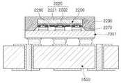
도면을 참조하면, 팬-아웃 반도체 패키지(2100)는, 예를 들면, 반도체칩(2120)의 외측이 봉합재(2130)로 보호되며, 반도체칩(2120)의 접속패드(2122)가 연결부재(2140)에 의하여 반도체칩(2120)의 바깥쪽까지 재배선된다. 이때, 연결부재(2140) 상에는 패시베이션층(2202)이 더 형성될 수 있으며, 패시베이션층(2202)의 개구부에는 언더범프금속층(2160)이 더 형성될 수 있다. 언더범프금속층(2160) 상에는 솔더볼(2170)이 더 형성될 수 있다. 반도체칩(2120)은 바디(2121), 접속패드(2122), 패시베이션막(미도시) 등을 포함하는 집적회로(IC)일 수 있다. 연결부재(2140)는 절연층(2141), 절연층(2241) 상에 형성된 재배선층(2142), 접속패드(2122)와 재배선층(2142) 등을 전기적으로 연결하는 비아(2143)를 포함할 수 있다.
In the fan-out
이와 같이, 팬-아웃 반도체 패키지는 반도체칩 상에 형성된 연결부재를 통하여 반도체칩의 바깥쪽에 까지 I/O 단자를 재배선하여 배치시킨 형태이다. 상술한 바와 같이, 팬-인 반도체 패키지는 반도체칩의 I/O 단자를 모두 반도체칩 안쪽에 배치시켜야 하고 이에 소자 사이즈가 작아지면 볼 크기와 피치를 줄여야 하므로 표준화된 볼 레이아웃을 사용할 수 없다. 반면, 팬-아웃 반도체 패키지는 이와 같이 반도체칩 상에 형성된 연결부재를 통하여 반도체칩의 바깥쪽에 까지 I/O 단자를 재배선하여 배치시킨 형태인바 반도체칩의 크기가 작아지더라도 표준화된 볼 레이아웃을 그대로 사용할 수 있는바, 후술하는 바와 같이 전자기기의 메인보드에 별도의 BGA 기판 없이도 실장될 수 있다.
As described above, the fan-out semiconductor package is formed by rewiring the I / O terminals to the outside of the semiconductor chip through the connecting member formed on the semiconductor chip. As described above, in the fan-in semiconductor package, all of the I / O terminals of the semiconductor chip must be disposed inside the semiconductor chip. If the element size is reduced, the ball size and pitch must be reduced. On the other hand, in the fan-out semiconductor package, the I / O terminals are rewired to the outside of the semiconductor chip through the connecting member formed on the semiconductor chip so that the size of the semiconductor chip is reduced. And can be mounted on a main board of an electronic device without a separate BGA substrate as will be described later.
도 8은 팬-아웃 반도체 패키지가 전자기기의 메인보드에 실장된 경우를 개략적으로 나타낸 단면도다.
8 is a cross-sectional view schematically showing a case where the fan-out semiconductor package is mounted on a main board of an electronic apparatus.
도면을 참조하면, 팬-아웃 반도체 패키지(2100)는 솔더볼(2170) 등을 통하여 전자기기의 메인보드(2500)에 실장될 수 있다. 즉, 상술한 바와 같이, 팬-아웃 반도체 패키지(2100)는 반도체칩(2120) 상에 반도체칩(2120)의 사이즈를 벗어나는 팬-아웃 영역까지 접속패드(2122)를 재배선할 수 있는 연결부재(2140)를 형성하기 때문에, 표준화된 볼 레이아웃을 그대로 사용할 수 있으며, 그 결과 별도의 BGA 기판 등 없이도 전자기기의 메인보드(2500)에 실장 될 수 있다.
Referring to the drawings, the fan-out
이와 같이, 팬-아웃 반도체 패키지는 별도의 BGA 기판 없이도 전자기기의 메인보드에 실장 될 수 있기 때문에, BGA 기판을 이용하는 팬-인 반도체 패키지 대비 두께를 얇게 구현할 수 있는바 소형화 및 박형화가 가능하다. 또한, 열 특성과 전기적 특성이 우수하여 모바일 제품에 특히 적합하다. 또한, 인쇄회로기판(PCB)을 이용하는 일반적인 POP(Package on Package) 타입 보다 더 컴팩트하게 구현할 수 있고, 휨 현상 발생으로 인한 문제를 해결할 수 있다.
Since the fan-out semiconductor package can be mounted on the main board of the electronic device without using a separate BGA substrate, the fan-out semiconductor package can be made thinner than the fan-in semiconductor package using the BGA substrate, and miniaturization and thinning are possible. In addition, it has excellent thermal characteristics and electrical characteristics and is particularly suitable for mobile products. In addition, it can be implemented more compactly than a general POP (Package on Package) type using a printed circuit board (PCB), and it is possible to solve a problem caused by a bending phenomenon.
한편, 팬-아웃 반도체 패키지는 이와 같이 반도체칩을 전자기기의 메인보드 등에 실장하기 위하여, 그리고 외부의 충격으로부터 반도체칩을 보호하기 위한 패키지 기술을 의미하는 것으로, 이와는 스케일, 용도 등이 상이하며, 팬-인 반도체 패키지가 내장되는 BGA 기판 등의 인쇄회로기판(PCB)과는 다른 개념이다.
On the other hand, the fan-out semiconductor package means a package technology for mounting the semiconductor chip on a main board or the like of an electronic device and protecting the semiconductor chip from an external impact, and the scale, (PCB) such as a BGA substrate in which a fan-in semiconductor package is embedded.
이하에서는, 스타퍼층에 의한 블라인드 리세스부를 갖는 프레임를 도입하여 제조된 팬-아웃 반도체 패키지에 대하여 도면을 참조하여 설명한다.
Hereinafter, a fan-out semiconductor package manufactured by introducing a frame having a blind recessed portion by a starter layer will be described with reference to the drawings.
도 9는 팬-아웃 반도체 패키지의 일례를 대략 나타낸 단면도다.9 is a cross-sectional view schematically showing an example of a fan-out semiconductor package.
도 10은 도 9의 팬-아웃 반도체 패키지의 개략적인 Ⅰ-Ⅰ' 절단 평면도다.
10 is a schematic sectional elevational-cut view of the fan-out semiconductor package of FIG.
도면을 참조하면, 일례에 따른 팬-아웃 반도체 패키지(100)는 제1측이 스타퍼층(112aM)으로 덮이며 제1측의 반대측인 제2측이 개구된 블라인드 형태의 리세스부(110H)를 갖는 프레임(110), 접속패드(120P)가 배치된 활성면 및 활성면의 반대측에 배치된 비활성면을 가지며 비활성면이 스타퍼층(112aM)에 부착되도록 리세스부(110H)에 배치된 반도체칩(120), 프레임(110) 및 반도체칩(120) 각각의 적어도 일부를 봉합하며 리세스부(110H)의 적어도 일부를 채우는 봉합재(130), 및 프레임(110)와 봉합재(130) 반도체칩(120)의 활성면 상에 배치된 연결부재(140)를 포함한다. 또한, 필요에 따라서 연결부재(140) 상에 배치되며 연결부재(140)의 재배선층(142a, 142b, 142c)의 적어도 일부를 노출시키는 개구부를 갖는 제1패시베이션층(151), 프레임(110) 상에 배치되며 프레임(110)의 배선층(112c)의 적어도 일부를 노출시키는 개구부를 갖는 제2패시베이션층(152), 제1패시베이션층(151)의 개구부 상에 배치되며 노출된 재배선층(142c)과 전기적으로 연결된 언더범프금속층(160), 및 언더범프금속층(160) 상에 배치되어 언더범프금속층(160)을 통하여 노출된 재배선층(142c)과 전기적으로 연결된 전기연결구조체(170)를 더 포함한다.
Referring to the drawings, a fan-out
한편, 프레임(110)는 접속비아층(113a, 113b, 113c)를 통하여 서로 전기적으로 연결된 배선층(112a, 112b, 112c, 112d)을 포함하고, 연결부재(140)는 접속비아(143a1, 143a2, 143b, 143c)를 통하여 서로 전기적으로 연결된 재배선층(142a, 142b, 142c)을 포함하며, 반도체칩(120)의 접속패드(120P)는 배선층(112a, 112b, 112c, 112d) 및 재배선층(142a, 142b, 142c)과 전기적으로 연결된다.
The
한편, 단순히 블라인드 형태의 리세스부를 갖는 프레임를 도입하고 리세스부에 반도체칩을 배치한 후 봉합하고 연결부재를 그 위에 형성하기 위해서는 반도체칩의 접속패드 상에 구리 범프 등을 미리 형성하여 두는 것이 필요하며, 이 경우 연결부재 형성을 위하여 편평한 면을 만들기 위하여 그라인딩 공정이 요구된다. 범프의 높이 단차를 일정하게 만들어줄 필요가 있기 때문이다. 그런데, 범프의 경우 그라인딩 되는 표면의 면적이 작기 때문에 그라인딩 공정 과정에서 범프를 구성하는 재질, 예컨대 구리(Cu) 등이 번지는 버(Burr) 현상이 발생할 수 있다. 그 결과, 예기치 못한 전기적인 단락이나 쇼트가 발생할 수 있다.
On the other hand, in order to merely introduce a frame having a recessed portion in the form of a blind, dispose a semiconductor chip on the recess portion, and form a connecting member thereon, it is necessary to previously form a copper bump or the like on the connection pad of the semiconductor chip In this case, a grinding process is required in order to make a flat surface for forming a connecting member. This is because it is necessary to make the height step of the bump constant. However, since the area of the surface to be ground is small in the case of bumps, a burr phenomenon may occur in which materials constituting the bumps, such as copper (Cu), are burnt during the grinding process. As a result, unexpected electrical shorts or shorts may occur.
반면, 일례에 따른 팬-아웃 반도체 패키지(100)는 후술하는 공정에서 알 수 있듯이 반도체칩(120)의 활성면에 수용성 폴리머(230)를 코팅하여 보호막을 형성한 상태로 블라인드 형태의 리세스부(110H)에 배치하며, 봉합 후에는 수용성 폴리머(230)를 세정공정 등을 통하여 제거한다. 이 경우 제거된 수용성 폴리머(230)에 의하여 반도체칩(120)의 활성면이 노출되기 때문에, 연결부재(140)의 절연층(141)이 반도체칩(120)의 활성면과 물리적으로 접할 수 있으며, 따라서 연결부재(140)를 그 위에 형성하는 경우 접속패드(120P)를 연결부재(140)의 절연층(141)을 관통하는 연결부재(140)의 접속비아(143a1)와 직접 연결시킬 수 있다. 즉, 별도의 범프 형성이 불필요하다. 따라서, 상술한 버 현상 등을 방지할 수 있다.
In the fan-out
이하, 일례에 따른 팬-아웃 반도체 패키지(100)에 포함되는 각각의 구성에 대하여 보다 자세히 설명한다.
Hereinafter, each configuration included in the fan-out
프레임(110)는 구체적인 재료에 따라 패키지(100)의 강성을 보다 개선시킬 수 있으며, 봉합재(130)의 두께 균일성 확보 등의 역할을 수행할 수 있다. 또한, 프레임(110)는 배선층(112a, 112b, 112c, 112d)과 접속비아층(113a, 113b, 113c)를 포함하는바 연결부재로의 역할을 수행할 수도 있다. 프레임(110)는 반도체칩(120)의 비활성면 상에 배치되는 배선층(112c)을 포함하는바, 별도의 백사이드 배선층의 형성 공정 없이도 반도체칩(120)을 위한 백사이드 배선층을 제공할 수 있다. 프레임(110)는 스타퍼층(112aM)을 스타퍼로 형성된 블라인드 형태의 리세스부(110H)를 가지며, 반도체칩(120)은 스타퍼층(112aM)에 비활성면이 다이부착필름(DAF: Die Attach Film)과 같은 공지의 접착부재(125) 등을 매개로 부착된다. 리세스부(110H)는 후술하는 바와 같이 샌드 블라스트 공정을 통하여 형성될 수 있으며, 이 경우 단면 형상이 테이퍼 형상일 수 있다. 즉, 리세스부(110H)의 벽면은 스타퍼층(112aM)을 기준으로 소정의 기울기를 가질 수 있다. 이 경우, 반도체칩(120)의 얼라인 공정이 보다 수월할 수 있는바, 수율이 높아질 수 있다.
The
프레임(110)는 제1절연층(111a), 제1절연층(111a)의 제1측 및 제2측에 각각 배치된 제1배선층(112a) 및 제2배선층(112b), 제1절연층(111a)의 제1측에 배치되어 제1배선층(112a)을 덮는 제2절연층(111b), 제2절연층(111b) 상에 배치된 제3배선층(112c), 제1절연층(111a)의 제2측에 배치되어 제2배선층(112b)을 덮는 제3절연층(111c), 및 제3절연층(111c) 상에 배치된 제4배선층(112d)을 포함한다. 또한, 제1절연층(111a)을 관통하며 제1 및 제2배선층(112a, 112b)을 전기적으로 연결하는 제1접속비아층(113a), 제2절연층(112b)을 관통하며 제1 및 제3배선층(112a, 112c)을 전기적으로 연결하는 제2접속비아층(113b), 및 제3절연층(111c)을 관통하며 제2 및 제4배선층(112b, 112d)을 전기적으로 연결하는 제3접속비아층(113c)를 포함한다. 제1 내지 제4배선층(112a, 112b, 112c, 112d)은 서로 전기적으로 연결되며, 각각 반도체칩(120)의 접속패드(120P)와 전기적으로 연결된다. 리세스부(110H)는 제1 및 제3절연층(111a, 111c)을 관통하되 제2절연층(111b)은 관통하지 않는다. 스타퍼층(112aM)은 제1절연층(111a)의 제1측에 배치되어 제2절연층(112b)으로 덮인다.
The
스타퍼층(112aM)은 구리(Cu) 등의 메탈을 포함하는 금속판일 수 있다. 또는, 메탈 보다 샌드 블라스트에 대한 에칭율이 작은 물질을 포함할 수도 있다. 예컨대, 드라이 필름 포토레지스트를 사용할 수도 있다. 스타퍼층(112aM)은 제1측이 상기 제2절연층으로 덮이되 제1측의 반대측인 제2측의 표면의 적어도 일부가 리세스부(110H)에 의하여 노출될 수 있다. 스타퍼층(112aM)은 제1절연층(111a)과 물리적으로 접하는 테두리 영역의 두께가 리세스부(110H)에 의하여 제1절연층(111a)으로부터 노출된 영역의 두께 보다 두꺼울 수 있다. 이는 샌드 블라스트 공정 과정에서 노출된 영역 역시 일부 제거될 수 있기 때문이다.
The stopper layer 112aM may be a metal plate including a metal such as copper (Cu). Alternatively, it may include a material having a lower etching rate for the sandblast than metal. For example, a dry film photoresist may be used. The first side of the stopper layer 112aM may be covered with the second insulating layer and at least a part of the surface of the second side opposite to the first side may be exposed by the
절연층(111a, 111b, 111c)의 재료로는 절연물질이 사용될 수 있는데, 이때 절연물질로는 에폭시 수지와 같은 열경화성 수지, 폴리이미드와 같은 열가소성 수지, 또는 이들 수지가 무기필러와 혼합되거나, 또는 무기필러와 함께 유리섬유(Glass Fiber, Glass Cloth, Glass Fabric) 등의 심재에 함침된 수지, 예를 들면, 프리프레그(prepreg), ABF(Ajinomoto Build-up Film), FR-4, BT(Bismaleimide Triazine) 등이 사용될 수 있다. 유리섬유 등을 포함하는 프리프레그와 같은 강성이 높은 자재를 사용하면, 프레임(110)를 패키지(100)의 워피지 제어를 위한 지지부재로도 활용 할 수 있다.
As the material of the insulating
제1절연층(111a)은 제2절연층(111b) 및 제3절연층(111c)보다 두께가 두꺼울 수 있다. 제1절연층(111a)은 기본적으로 강성 유지를 위하여 상대적으로 두꺼울 수 있으며, 제2절연층(111b) 및 제3절연층(111c)은 더 많은 수의 배선층(112c, 112d)을 형성하기 위하여 도입된 것일 수 있다. 제1절연층(111a)은 제2절연층(111b) 및 제3절연층(111c)과 상이한 절연물질 포함할 수 있다. 예를 들면, 제1절연층(111a)은 절연수지가 무기필러와 함께 유리섬유에 함침된, 예컨대, 프리프레그일 수 있고, 제2절연층(111c) 및 제3절연층(111c)은 무기필러 및 절연수지를 포함하는 ABF 필름 또는 PID 필름일 수 있으나, 이에 한정되는 것은 아니다. 유사한 관점에서, 제1절연층(111a)을 관통하는 제1접속비아층(113a)는 제2 및 제3절연층(111b, 111c)을 관통하는 제2 및 제3접속비아층(113b, 113c)보다 직경이 클 수 있다.
The first insulating
배선층(112a, 112b, 112c, 112d)은 재배선층(142a, 142b, 142c)과 함께 반도체칩(120)의 접속패드(120P)를 재배선할 수 있다. 배선층(112a, 112b, 112c, 112d) 각각의 형성물질로는 구리(Cu), 알루미늄(Al), 은(Ag), 주석(Sn), 금(Au), 니켈(Ni), 납(Pb), 티타늄(Ti), 또는 이들의 합금 등의 도전성 물질을 사용할 수 있다. 배선층(112a, 112b, 112c, 112d)은 해당 층의 설계 디자인에 따라 다양한 기능을 수행할 수 있다. 예를 들면, 그라운드(GrouND: GND) 패턴, 파워(PoWeR: PWR) 패턴, 신호(Signal: S) 패턴 등을 포함할 수 있다. 여기서, 신호(S) 패턴은 그라운드(GND) 패턴, 파워(PWR) 패턴 등을 제외한 각종 신호, 예를 들면, 데이터 신호 등을 포함한다. 또한, 각종 패드패턴을 포함할 수 있다.
The
배선층(112a, 112b, 112c, 112d)의 두께는 연결부재(140)의 재배선층(142a, 142b, 142c)의 두께보다 두꺼울 수 있다. 프레임(110)는 반도체칩(120) 이상의 두께를 가질 수 있는바, 배선층(112a, 112b, 112c, 112d) 역시 보다 큰 사이즈로 형성할 수 있다. 반면, 연결부재(140)의 재배선층(142a, 142b, 142c)은 박형화를 위하여 보다 상대적으로 작은 사이즈로 형성할 수 있다.
The thickness of the
접속비아층(113a, 113b, 113c)는 서로 다른 층에 형성된 배선층(112a, 112b, 112c, 112d)을 전기적으로 연결시키며, 그 결과 프레임(110) 내에 전기적 경로를 형성시킨다. 접속비아층(113a, 113b, 113c) 역시 형성물질로는 도전성 물질을 사용할 수 있다. 접속비아층(113a, 113b, 113c)는 도전성 물질로 완전히 충전될 수 있으며, 또는 도전성 물질이 비아 홀의 벽면을 따라 형성된 것일 수도 있다. 제1접속비아층(113a)는 원기둥 단면 형상이나 모래시계 단면 형상을 가질 수 있고, 제2 및 제3접속비아층(113b, 113c)는 테이퍼 단면 형상을 가질 수 있다. 이때, 제2 및 제3접속비아층(113b, 113c)는 제1절연층(111a)을 기준으로 서로 반대 방향의 테이퍼 단면 형상을 가질 수 있다.
The connection via
반도체칩(120)은 소자 수백 내지 수백만 개 이상이 하나의 칩 안에 집적화된 집적회로(IC: Integrated Circuit)일 수 있다. 반도체칩(120)은, 예를 들면, 센트랄 프로세서(예컨대, CPU), 그래픽 프로세서(예컨대, GPU), 필드 프로그램어블 게이트 어레이(FPGA), 디지털 신호 프로세서, 암호화 프로세서, 마이크로 프로세서, 마이크로 컨트롤러 등의 프로세서칩, 구체적으로는 어플리케이션 프로세서(AP: Application Processor)일 수 있으나, 이에 한정되는 것은 아니다.
The
반도체칩(120)은 액티브 웨이퍼를 기반으로 형성된 것일 수 있으며, 이 경우 바디를 이루는 모재로는 실리콘(Si), 게르마늄(Ge), 갈륨비소(GaAs) 등이 사용될 수 있다. 바디에는 다양한 회로가 형성되어 있을 수 있다. 접속패드(120P)는 반도체칩(120)을 다른 구성요소와 전기적으로 연결시키기 위한 것으로, 형성물질로는 알루미늄(Al) 등의 도전성 물질을 특별한 제한 없이 사용할 수 있다. 바디 상에는 접속패드(120P)를 노출시키는 산화막 또는 질화막 등의 패시베이션막이 형성될 수 있으며, 패시베이션막은 산화막과 질화막의 이중층일 수도 있다. 기타 필요한 위치에 절연막 등이 더 배치될 수도 있다. 반도체칩(120)은 베어 다이(Bare Die)일 수 있으나, 필요에 따라서는, 활성면 상에 재배선층이 더 형성될 수 있다.
The
봉합재(130)는 프레임(110), 반도체칩(120) 등을 보호할 수 있다. 봉합형태는 특별히 제한되지 않으며, 프레임(110), 반도체칩(120) 등의 적어도 일부를 감싸는 형태이면 무방하다. 예를 들면, 봉합재(130)는 프레임(110)의 적어도 일부를 덮을 수 있으며, 리세스부(110H)의 벽면과 반도체칩(120)의 측면 사이의 공간을 채울 수 있다. 봉합재(130)가 리세스부(110H)를 채움으로써, 구체적인 물질에 따라 접착제 역할을 수행함과 동시에 버클링을 감소시킬 수 있다.
The sealing
봉합재(130)의 재료는 특별히 한정되는 않는다. 예를 들면, 절연물질이 사용될 수 있는데, 이때 절연물질로는 에폭시 수지와 같은 열경화성 수지, 폴리이미드와 같은 열가소성 수지, 또는 이들 수지가 무기필러와 혼합되거나, 또는 무기필러와 함께 유리섬유(Glass Fiber, Glass Cloth, Glass Fabric) 등의 심재에 함침된 수지, 예를 들면, 프리프레그(prepreg), ABF(Ajinomoto Build-up Film), FR-4, BT(Bismaleimide Triazine) 등이 사용될 수 있다. 필요에 따라서는, 감광성 절연(Photo Imagable Encapsulant: PIE) 수지를 사용할 수도 있다.
The material of the sealing
연결부재(140)는 반도체칩(120)의 접속패드(120P)를 재배선할 수 있으며, 프레임(110)의 배선층(112a, 112b, 112c, 112d)을 반도체칩(120)의 접속패드(120P)와 전기적으로 연결할 수 있다. 연결부재(140)를 통해 다양한 기능을 갖는 수십 수백만 개의 접속패드(120P)가 재배선 될 수 있으며, 전기연결구조체(170)를 통하여 그 기능에 맞춰 외부에 물리적 및/또는 전기적으로 연결될 수 있다.
The
연결부재(140)는 프레임(110)와 봉합재(130)와 반도체칩(120)의 활성면 상에 배치된 제1절연층(141a), 제1절연층(141a) 상에 배치된 제1재배선층(142a), 제1절연층(141a)을 관통하며 제1재배선층(142a)을 접속패드(120P) 및 제4배선층(112d)과 전기적으로 연결하는 제1접속비아(143a1, 143b1), 제1절연층(141a) 상에 배치되어 제1재배선층(142a)을 덮는 제2절연층(141b), 제2절연층(141b) 상에 배치된 제2재배선층(142b), 제2절연층(141b)를 관통하며 제1 및 제2재배선층(142a, 142b)을 전기적으로 연결하는 제2접속비아(143b), 제2절연층(111b) 상에 배치되어 제2재배선층(142b)을 덮는 제3절연층(141c), 제3절연층(141c) 상에 배치된 제3재배선층(142c), 제3절연층(141c)를 관통하며 제2 및 제3재배선층(142b, 142c)을 전기적으로 연결하는 제3접속비아(143c)를 포함한다. 연결부재(140)의 절연층과 재배선층과 비아층은 보다 많은 수의 층으로, 또는 보다 적은 수의 층으로 구성될 수 있다.
The connecting
절연층(141a, 141b, 141c)의 물질로는 절연물질이 사용될 수 있는데, 이때 절연물질로는 상술한 바와 같은 절연물질 외에도 PID(Photo Image-able Dielectric) 수지와 같은 감광성 절연물질을 사용할 수도 있다. 즉, 절연층(141a, 141b, 141c)은 각각 감광성 절연층일 수 있다. 절연층(141a, 141b, 141c)이 감광성의 성질을 갖는 경우, 절연층(141a, 141b, 141c)을 보다 얇게 형성할 수 있으며, 보다 용이하게 접속비아(143a1, 143a2, 143b, 143c)의 파인 피치를 달성할 수 있다. 절연층(141a, 141b, 141c)은 각각 절연수지 및 무기필러를 포함하는 감광성 절연층일 수 있다. 절연층(141a, 141b, 141c)이 다층인 경우, 이들의 물질은 서로 동일할 수 있고, 필요에 따라서는 서로 상이할 수도 있다. 절연층(141a, 141b, 141c)이 다층인 경우, 이들은 공정에 따라 일체화 되어 이들 자체로는 경계가 불분명할 수도 있다.
As the material of the insulating
후술하는 공정에서 알 수 있듯이, 반도체칩(120)의 활성면에 수용성 폴리머(230)를 코팅하여 보호막을 형성한 상태로 블라인드 형태의 리세스부(110H)에 배치하며, 봉합 후에는 수용성 폴리머(230)를 세정공정 등을 통하여 제거한다. 이 경우 제거된 수용성 폴리머(230)에 의하여 반도체칩(120)의 활성면이 노출되기 때문에, 제1절연층(141a)을 반도체칩(120)의 활성면 상에 직접 형성할 수 있다. 그 결과, 제1절연층(141a)과 봉합재(130)의 경계면은 제1절연층(141a)과 반도체칩(120)의 활성면의 경계면과 단차(h)를 가진다. 구체적으로, 제1절연층(141a)과 봉합재(130)의 경계면은 제1절연층(141a)과 반도체칩(120)의 활성면의 경계면 보다 스타퍼층(112aM)으로부터 더 멀게 위치한다.
As will be described later, the active surface of the
재배선층(142a, 142b, 142c)은 실질적으로 접속패드(120P)를 재배선하는 역할을 수행할 수 있으며, 형성물질로는 구리(Cu), 알루미늄(Al), 은(Ag), 주석(Sn), 금(Au), 니켈(Ni), 납(Pb), 티타늄(Ti), 또는 이들의 합금 등의 도전성 물질을 사용할 수 있다. 재배선층(142a, 142b, 142c)은 해당 층의 설계 디자인에 따라 다양한 기능을 수행할 수 있다. 예를 들면, 그라운드(GrouND: GND) 패턴, 파워(PoWeR: PWR) 패턴, 신호(Signal: S) 패턴 등을 포함할 수 있다. 여기서, 신호(S) 패턴은 그라운드(GND) 패턴, 파워(PWR) 패턴 등을 제외한 각종 신호, 예를 들면, 데이터 신호 등을 포함한다. 또한, 각종 패드패턴을 포함할 수 있다.
The rewiring layers 142a, 142b and 142c can substantially rewire the
접속비아(143a1, 143a2, 143b, 143c)는 서로 다른 층에 형성된 재배선층(142a, 142b, 142c), 접속패드(120P), 제4배선층(112d) 등을 전기적으로 연결시키며, 그 결과 패키지(100) 내에 전기적 경로를 형성시킨다. 접속비아(143a1, 143a2, 143b, 143c)의 형성 물질로는 구리(Cu), 알루미늄(Al), 은(Ag), 주석(Sn), 금(Au), 니켈(Ni), 납(Pb), 티타늄(Ti), 또는 이들의 합금 등의 도전성 물질을 사용할 수 있다. 접속비아(143a1, 143a2, 143b, 143c)는 도전성 물질로 완전히 충전될 수 있으며, 또는 도전성 물질이 비아의 벽을 따라 형성된 것일 수도 있다. 또한, 테이퍼 단면 형상 등을 가질 수 있다. 상술한 단차(h)에 의하여, 제1-1접속비아(143a1)의 높이는 제1-2접속비아(143b2) 높이보다 클 수 있다. 또한, 접속패드(120P)는 별도의 범프 없이 제1-1접속비아(143a1)와 물리적으로 접할 수 있다.
The connection vias 143a1, 143a2, 143b and 143c electrically connect the
제1패시베이션층(151)은 연결부재(140)를 외부의 물리적 화학적 손상 등으로부터 보호할 수 있다. 제1패시베이션층(151)은 연결부재(140)의 재배선층(142a, 142b, 142c)의 적어도 일부를 노출시키는 개구부를 가질 수 있다. 이러한 개구부는 제1패시베이션층(151)에 수십 내지 수백만 개 형성될 수 있다. 제1패시베이션층(151)의 재료는 특별히 한정되는 않는다. 예를 들면, 절연물질이 사용될 수 있는데, 이때 절연물질로는 에폭시 수지와 같은 열경화성 수지, 폴리이미드와 같은 열가소성 수지, 또는 이들 수지가 무기필러와 혼합되거나, 또는 무기필러와 함께 유리섬유(Glass Fiber, Glass Cloth, Glass Fabric) 등의 심재에 함침된 수지, 예를 들면, 프리프레그(prepreg), ABF(Ajinomoto Build-up Film), FR-4, BT(Bismaleimide Triazine) 등이 사용될 수 있다. 또는, 솔더레지스트(Solder Resist)가 사용될 수도 있다.
The
제2패시베이션층(152)은 프레임(110)를 외부의 물리적 화학적 손상 등으로부터 보호할 수 있다. 제2패시베이션층(152)은 프레임(110)의 제3배선층(112c)의 적어도 일부를 노출시키는 개구부를 가질 수 있다. 이러한 개구부는 제2패시베이션층(152)에 수십 내지 수백만 개 형성될 수 있다. 제2패시베이션층(152)의 재료는 특별히 한정되는 않는다. 예를 들면, 절연물질이 사용될 수 있는데, 이때 절연물질로는 에폭시 수지와 같은 열경화성 수지, 폴리이미드와 같은 열가소성 수지, 또는 이들 수지가 무기필러와 혼합되거나, 또는 무기필러와 함께 유리섬유(Glass Fiber, Glass Cloth, Glass Fabric) 등의 심재에 함침된 수지, 예를 들면, 프리프레그(prepreg), ABF(Ajinomoto Build-up Film), FR-4, BT(Bismaleimide Triazine) 등이 사용될 수 있다. 또는, 솔더레지스트(Solder Resist)가 사용될 수도 있다.
The
언더범프금속층(160)은 전기연결구조체(170)의 접속 신뢰성을 향상시켜주며, 그 결과 패키지(100)의 보드 레벨 신뢰성을 개선해준다. 언더범프금속층(160)은 제1패시베이션층(151)의 개구부를 통하여 노출된 연결부재(140)의 재배선층(142c)과 연결된다. 언더범프금속층(160)은 제1패시베이션층(151)의 개구부에 공지의 도전성 물질, 즉 금속을 이용하여 공지의 메탈화(Metallization) 방법으로 형성할 수 있으나, 이에 한정되는 것은 아니다.
The
전기연결구조체(170)는 팬-아웃 반도체 패키지(100)를 외부와 물리적 및/또는 전기적으로 연결시킨다. 예를 들면, 팬-아웃 반도체 패키지(100)는 전기연결구조체(170)를 통하여 전자기기의 메인보드에 실장될 수 있다. 전기연결구조체(170)는 도전성 물질, 예를 들면, 솔더(solder) 등으로 형성될 수 있으나, 이는 일례에 불과하며 재질이 특별히 이에 한정되는 것은 아니다. 전기연결구조체(170)는 랜드(land), 볼(ball), 핀(pin) 등일 수 있다. 전기연결구조체(170)는 다중층 또는 단일층으로 형성될 수 있다. 다중층으로 형성되는 경우에는 구리 필라(pillar) 및 솔더를 포함할 수 있으며, 단일층으로 형성되는 경우에는 주석-은 솔더나 구리를 포함할 수 있으나, 역시 이는 일례에 불과하며 이에 한정되는 것은 아니다.
The
전기연결구조체(170)의 개수, 간격, 배치 형태 등은 특별히 한정되지 않으며, 통상의 기술자에게 있어서 설계 사항에 따라 충분히 변형이 가능하다. 예를 들면, 전기연결구조체(170)의 수는 접속패드(120P)의 수에 따라서 수십 내지 수천 개일 수 있으며, 그 이상 또는 그 이하의 수를 가질 수도 있다. 전기연결구조체(170)가 솔더볼인 경우, 전기연결구조체(170)는 언더범프금속층(160)의 제1패시베이션층(151)의 일면 상으로 연장되어 형성된 측면을 덮을 수 있으며, 접속 신뢰성이 더욱 우수할 수 있다.
The number, spacing, arrangement type, etc. of the
전기연결구조체(170) 중 적어도 하나는 팬-아웃 영역에 배치된다. 팬-아웃 영역이란 반도체칩(120)이 배치된 영역을 벗어나는 영역을 의미한다. 팬-아웃(fan-out) 패키지는 팬-인(fan-in) 패키지에 비하여 신뢰성이 우수하고, 다수의 I/O 단자 구현이 가능하며, 3D 인터코넥션(3D interconnection)이 용이하다. 또한, BGA(Ball Grid Array) 패키지, LGA(Land Grid Array) 패키지 등과 비교하여 패키지 두께를 얇게 제조할 수 있으며, 가격 경쟁력이 우수하다.
At least one of the
한편, 도면에는 도시하지 않았으나, 필요에 따라서는 리세스부(110H)의 벽면에 방열 및/또는 전자파 차폐 목적으로 금속박막을 형성할 수 있다. 또한, 필요에 따라서는 리세스부(110H) 내에 서로 동일하거나 상이한 기능을 수행하는 복수의 반도체칩(120)을 배치할 수도 있다. 또한, 필요에 따라서는 리세스부(110H) 내에 별도의 수동부품, 예컨대 인덕터나 커패시터 등을 배치할 수도 있다. 또한, 필요에 따라서는 패시베이션층(151, 152) 표면 상에 수동부품, 예컨대 인덕터나 커패시터 등을 포함하는 표면실장(SMT) 부품을 배치할 수도 있다.
Although not shown in the drawings, a metal thin film may be formed on the wall surface of the
도 11 내지 도 16은 도 9의 팬-아웃 반도체 패키지의 제조 과정을 개략적으로 나타낸 공정도다.
FIGS. 11 to 16 are schematic views showing a manufacturing process of the fan-out semiconductor package of FIG.
도 11을 참조하면, 먼저, 동박적층판(CCL: Copper Clad Laminated) 등을 이용하여 제1절연층(111a)을 준비하고, 제1절연층(111a)에 공지의 도금 공정을 이용하여 제1 및 제2배선층(112a, 112b)과 스타퍼층(112aM)과 제1접속비아층(113a)를 형성한다. 제1접속비아층(113a)를 위한 비아홀은 기계적 드릴 및/또는 레이저 드릴 등을 이용하여 형성할 수 있다. 다음으로, 제1절연층(111a)의 양면에 제2 및 제3절연층(111b, 111c)을 형성한다. 제2 및 제3절연층(111b, 111c)은 ABF 등을 라미네이션하고 경화하는 방법으로 형성할 수 있다. 다음으로, 제2 및 제3절연층(111b, 111c)에 각각 공지의 도금 공정을 이용하여 제3및 제4배선층(112c, 112d)과 제2 및 제3접속비아층(113a, 113b)를 형성한다. 제2 및 제3접속비아층(113b, 113c)를 위한 비아홀 역시 기계적 드릴 및/또는 레이저 드릴 등을 이용하여 형성할 수 있다. 일련의 과정으로 준비된 프레임(110)의 제1측에 제2패시베이션층(152)을 부착하고, 제2패시베이션층(152) 상에 절연층(201)과 금속층(202)을 포함하는, 예컨대 DCF 등의 캐리어 필름(200)을 부착한다. 제2패시베이션층(152)은 GCP 자재를 이용하여 도입할 수 있다. 또한, DFR과 같은 드라이 필름(250)을 프레임(110)의 제2측에 부착한다.
11, first, a first insulating
도 12를 참조하면, 다음으로, 샌드 블라스트를 이용하여 제1 및 제3절연층(111a, 111c)을 관통하는 리세스부(110H)를 형성한다. 이때 스타퍼층(112aM)은 스타퍼(stopper)로 기능하다. 형성된 리세스부(110H)는 테이퍼 단면 형상을 가질 수 있다. 리세스부(110H)를 형성한 후에는 드라이 필름(250)을 제거한다.
Referring to FIG. 12, a
도 13을 참조하면, 다음으로, 스타퍼층(112aM)에 반도체칩(120)을 비활성면이 부착되도록 리세스부(110H)에 배치한다. 부착에는 다이부착필름(DAF)과 같은 공지의 접착부재(125)를 이용할 수 있다. 한편, 반도체칩(120)은 활성면 상에 수용성 폴리머(230)를 코팅하여 보호막을 형성한 상태로 부착한다. 다음으로, 봉합재(130)를 이용하여 프레임(110)와 반도체칩(120)의 적어도 일부를 봉합한다. 봉합재(130)는 ABF 등을 라미네이션한 후 경화하는 방법으로 형성할 수 있다.
Referring to FIG. 13, the
도 14를 참조하면, 그 후, 제4배선층(112d)의 표면과 코팅된 수용성 폴리머(230)의 표면이 노출되도록 봉합재(130)를 그라인딩(Grinding) 한다. 그라인딩에 의하여 봉합재(130)의 표면이 평평해지며, 코팅된 수용성 폴리머(230)의 표면과 제4배선층(112d)의 표면이 봉합재(130)로부터 노출되게 된다.
Referring to FIG. 14, the sealing
도 15를 참조하면, 다음으로, 세정 공정을 진행하여 코팅된 수용성 폴리머(230)를 제거한다. 그 결과 상술한 단차(h)가 형성된다. 다음으로, 봉합재(130) 및 노출된 반도체칩(120)의 활성면 상에 PID를 도포 및 경화하여 제1절연층(141a)을 형성하고, 도금 공정으로 제1재배선층(142a) 및 제1접속비아(143a1, 143a2)를 형성한다. 비아홀은 노광 및 현상을 이용하는 포토리소그래피 법으로 형성할 수 있다.
Referring to FIG. 15, next, a cleaning process is performed to remove the coated water-
도 16을 참조하면, 계속하여, 제2 및 제3절연층(141b, 141c)과 제2 및 제3재배선층(142b, 142c)과 제2 및 제3접속비아(143b, 143c)를 설계에 따라서 보다 많은 층수로 형성한다. 일련의 과정으로 연결부재(140)가 형성된다. 다음으로, 연결부재(140) 상에 제1패시베이션층(151)을 ABF 등을 라미네이션한 후 경화하여 형성하고, 캐리어 필름(200)은 제거한다. 다음으로, 공지의 메탈화 방법으로 언더범프금속층(160)을 형성하고, 솔더볼 등을 이용한 리플로우 공정 등으로 전기연결구조체(170)를 형성한다. 일련의 과정을 통하여 일례에 따른 팬-아웃 반도체 패키지(100)가 제조된다.
16, the second and third insulating
본 개시에서 하측, 하부, 하면 등은 편의상 도면의 단면을 기준으로 팬-아웃 반도체 패키지의 실장 면을 향하는 방향을 의미하는 것으로 사용하였고, 상측, 상부, 상면 등은 그 반대 방향으로 사용하였다. 다만, 이는 설명의 편의상 방향을 정의한 것으로, 특허청구범위의 권리범위가 이러한 방향에 대한 기재에 의하여 특별히 한정되는 것이 아님은 물론이다.
In the present disclosure, the lower side, the lower side, the lower side and the like refer to the direction toward the mounting surface of the fan-out semiconductor package with reference to the cross section of the drawing for convenience, and the upper side, the upper side and the upper side are used in the opposite direction. It should be noted, however, that this is a definition of a direction for the sake of convenience of explanation, and it is needless to say that the scope of rights of the claims is not particularly limited by description of such direction.
본 개시에서 연결된다는 의미는 직접 연결된 것뿐만 아니라, 접착제 층 등을 통하여 간접적으로 연결된 것을 포함하는 개념이다. 또한, 전기적으로 연결된다는 의미는 물리적으로 연결된 경우와 연결되지 않은 경우를 모두 포함하는 개념이다. 또한, 제1, 제2 등의 표현은 한 구성요소와 다른 구성요소를 구분 짓기 위해 사용되는 것으로, 해당 구성요소들의 순서 및/또는 중요도 등을 한정하지 않는다. 경우에 따라서는 권리범위를 벗어나지 않으면서, 제1 구성요소는 제2 구성요소로 명명될 수도 있고, 유사하게 제2 구성요소는 제1 구성요소로 명명될 수도 있다.
The meaning of being connected in this disclosure includes not only a direct connection but also an indirect connection through an adhesive layer or the like. In addition, the term "electrically connected" means a concept including both a physical connection and a non-connection. Also, the first, second, etc. expressions are used to distinguish one component from another, and do not limit the order and / or importance of the components. In some cases, without departing from the scope of the right, the first component may be referred to as a second component, and similarly, the second component may be referred to as a first component.
본 개시에서 사용된 일례 라는 표현은 서로 동일한 실시 예를 의미하지 않으며, 각각 서로 다른 고유한 특징을 강조하여 설명하기 위해서 제공된 것이다. 그러나, 상기 제시된 일례들은 다른 일례의 특징과 결합되어 구현되는 것을 배제하지 않는다. 예를 들어, 특정한 일례에서 설명된 사항이 다른 일례에서 설명되어 있지 않더라도, 다른 일례에서 그 사항과 반대되거나 모순되는 설명이 없는 한, 다른 일례에 관련된 설명으로 이해될 수 있다.
The expression " exemplary " used in this disclosure does not mean the same embodiment but is provided for emphasizing and explaining different unique features. However, the above-mentioned examples do not exclude that they are implemented in combination with the features of other examples. For example, although the description in the specific example is not described in another example, it can be understood as an explanation related to another example, unless otherwise described or contradicted by the other example.
본 개시에서 사용된 용어는 단지 일례를 설명하기 위해 사용된 것으로, 본 개시를 한정하려는 의도가 아니다. 이때, 단수의 표현은 문맥상 명백하게 다르게 뜻하지 않는 한, 복수의 표현을 포함한다.
The terms used in this disclosure are used only to illustrate an example and are not intended to limit the present disclosure. Wherein the singular expressions include plural expressions unless the context clearly dictates otherwise.
삭제delete
Claims (21)
Translated fromKorean접속패드와 상기 접속패드가 배치된 활성면 및 상기 활성면의 반대측인 비활성면을 가지며, 상기 비활성면이 상기 스타퍼층과 연결되도록 상기 리세스부에 배치된 반도체칩;
상기 반도체칩의 적어도 일부를 덮으며, 상기 리세스부의 적어도 일부를 채우는 봉합재; 및
상기 프레임과 상기 봉합재와 상기 반도체칩의 활성면 상에 배치된 제1절연층, 상기 제1절연층 상에 배치된 제1재배선층, 및 상기 제1절연층을 관통하며 상기 제1재배선층과 상기 접속패드를 전기적으로 연결하는 제1접속비아를 포함하는 연결부재; 를 포함하며,
상기 제1절연층과 상기 봉합재의 경계면은 상기 제1절연층과 상기 반도체칩의 활성면의 경계면과 단차를 갖는,
팬-아웃 반도체 패키지.
And at least one connecting via layer electrically connected to the one or more wiring layers through the one or more insulating layers, wherein a starter layer is disposed on the bottom surface of the insulating layer A frame having a recessed portion;
A semiconductor chip having a connection pad, an active surface on which the connection pad is disposed, and an inactive surface opposite to the active surface, the inactive surface being connected to the stopper layer;
A sealing material covering at least a part of the semiconductor chip and filling at least a part of the recessed part; And
A first rewiring layer disposed on the frame, the sealant, and a first insulating layer disposed on an active surface of the semiconductor chip; a first rewiring layer disposed on the first insulating layer; and a second rewiring layer disposed on the first rewiring layer, And a first connection via for electrically connecting the connection pad; / RTI >
Wherein the interface between the first insulating layer and the sealing material has a step difference from an interface between the first insulating layer and the active surface of the semiconductor chip,
A fan-out semiconductor package.
상기 연결부재는 상기 제1절연층을 관통하며 상기 제1재배선층과 상기 한층 이상의 배선층 중 최상측 배선층을 전기적으로 연결하는 제2접속비아를 더 포함하는,
팬-아웃 반도체 패키지.
The method according to claim 1,
Wherein the connecting member further includes a second connecting via which penetrates the first insulating layer and electrically connects the first rewiring layer and the uppermost wiring layer among the wiring layers of the one or more layers,
A fan-out semiconductor package.
상기 반도체칩의 활성면과 수직한 방향으로 바라 보았을 때,
팬-인 영역에서의 제1절연층의 두께와 팬-아웃 영역에서의 제2절연층의 두께가 상이한,
팬-아웃 반도체 패키지.
The method according to claim 1,
When viewed in a direction perpendicular to the active surface of the semiconductor chip,
Wherein the thickness of the first insulating layer in the fan-in region is different from the thickness of the second insulating layer in the fan-out region,
A fan-out semiconductor package.
상기 팬-인 영역에서의 제1절연층의 두께가 팬-아웃 영역에서의 제2절연층의 두께보다 두꺼운,
팬-아웃 반도체 패키지.
The method of claim 3,
Wherein a thickness of the first insulating layer in the fan-in area is greater than a thickness of the second insulating layer in the fan-out area,
A fan-out semiconductor package.
상기 제1접속비아와 상기 제2접속비아의 높이가 서로 상이한,
팬-아웃 반도체 패키지.
3. The method of claim 2,
Wherein the height of the first connection via and the height of the second connection via are different from each other,
A fan-out semiconductor package.
상기 제1접속비아의 높이가 상기 제2접속비아의 높이보다 큰,
팬-아웃 반도체 패키지.
6. The method of claim 5,
The height of the first connection via is greater than the height of the second connection via,
A fan-out semiconductor package.
상기 제1절연층은 감광성 절연물질(PID)을 포함하는,
팬-아웃 반도체 패키지.
The method according to claim 1,
Wherein the first insulating layer comprises a photosensitive insulating material (PID).
A fan-out semiconductor package.
접속패드와 상기 접속패드가 배치된 활성면 및 상기 활성면의 반대측인 비활성면을 가지며, 상기 비활성면이 상기 스타퍼층과 연결되도록 상기 리세스부에 배치된 반도체칩;
상기 반도체칩의 적어도 일부를 덮으며, 상기 리세스부의 적어도 일부를 채우는 봉합재; 및
상기 프레임 및 상기 반도체칩의 활성면 상에 배치되며, 상기 프레임의 복수의 배선층 및 상기 반도체칩의 접속패드를 전기적으로 연결시키는 재배선층을 포함하는 연결부재; 를 포함하며,
상기 복수의 절연층은 코어 절연층, 상기 코어 절연층의 하측에 배치된 하나 이상의 제1빌드업 절연층, 및 상기 코어 절연층의 상측에 배치된 하나 이상의 제2빌드업 절연층을 포함하며,
상기 코어 절연층은 상기 제1 및 제2빌드업 절연층 각각 보다 두께가 두꺼운,
팬-아웃 반도체 패키지.
A plurality of insulating layers, a plurality of wiring layers disposed in the plurality of insulating layers, and a plurality of connecting via layers passing through the plurality of insulating layers and electrically connecting the plurality of wiring layers, wherein a starter layer A frame having a recessed portion disposed therein;
A semiconductor chip having a connection pad, an active surface on which the connection pad is disposed, and an inactive surface opposite to the active surface, the inactive surface being connected to the stopper layer;
A sealing material covering at least a part of the semiconductor chip and filling at least a part of the recessed part; And
A connecting member disposed on the frame and an active surface of the semiconductor chip, the connecting member including a plurality of wiring layers of the frame and a re-wiring layer electrically connecting the connection pads of the semiconductor chip; / RTI >
Wherein the plurality of insulating layers includes a core insulating layer, at least one first build-up insulating layer disposed below the core insulating layer, and at least one second build-up insulating layer disposed over the core insulating layer,
Wherein the core insulation layer is thicker than each of the first and second build-up insulation layers,
A fan-out semiconductor package.
상기 제1빌드업 절연층의 층수와 상기 제2빌드업 절연층의 층수가 동일한,
팬-아웃 반도체 패키지.
9. The method of claim 8,
Wherein the number of layers of the first build-up insulation layer and the number of layers of the second build-
A fan-out semiconductor package.
상기 리세스부는 적어도 상기 코어 절연층을 관통하며, 상기 하나 이상의 제1 및 제2빌드업 절연층 중 적어도 하나의 빌드업 절연층을 관통하는,
팬-아웃 반도체 패키지.
9. The method of claim 8,
Wherein the recess portion extends through at least the core insulation layer and penetrates through at least one build-up insulation layer of the at least one first and second build-
A fan-out semiconductor package.
상기 제1빌드업 절연층을 관통하는 제1접속바이와 상기 제2빌드업 절연층을 관통하는 제2접속비아는 서로 반대 방향으로 테이퍼진,
팬-아웃 반도체 패키지.
9. The method of claim 8,
Wherein a first connection via through the first build-up insulation layer and a second connection via through the second build-up insulation layer are tapered in opposite directions,
A fan-out semiconductor package.
상기 리세스부의 벽면이 테이퍼진,
팬-아웃 반도체 패키지.
9. The method of claim 8,
Wherein a wall surface of the recessed portion is tapered,
A fan-out semiconductor package.
상기 반도체칩의 비활성면은 상기 스타퍼층에 접착부재를 통하여 부착된,
팬-아웃 반도체 패키지.
9. The method of claim 8,
Wherein an inactive surface of the semiconductor chip is attached to the starter layer through an adhesive member,
A fan-out semiconductor package.
상기 스타퍼층은 금속층이며,
상기 복수의 배선층 중 적어도 하나의 배선층은 그라운드를 포함하며,
상기 금속층은 상기 그라운드와 전기적으로 연결된,
팬-아웃 반도체 패키지.
9. The method of claim 8,
The starter layer is a metal layer,
Wherein at least one wiring layer among the plurality of wiring layers includes a ground,
Wherein the metal layer is electrically connected to the ground,
A fan-out semiconductor package.
상기 스타퍼층은 상기 반도체칩의 비활성면 보다 평면적이 넓은,
팬-아웃 반도체 패키지.
9. The method of claim 8,
Wherein the stopper layer has a planar shape that is wider than an inactive surface of the semiconductor chip,
A fan-out semiconductor package.
상기 리세스부의 바닥면은 상기 반도체칩의 비활성면 보다 평면적이 넓은,
팬-아웃 반도체 패키지.
9. The method of claim 8,
Wherein the bottom surface of the recessed portion is wider than the inactive surface of the semiconductor chip,
A fan-out semiconductor package.
상기 스타퍼층은 상기 리세스부에 의하여 노출된 영역의 두께가 노출되지 않는 테두리 영역의 두께보다 얇은,
팬-아웃 반도체 패키지.
9. The method of claim 8,
Wherein the stopper layer is thinner than a thickness of a border region where the thickness of the region exposed by the recess portion is not exposed,
A fan-out semiconductor package.
상기 프레임의 복수의 배선층 중 최상측의 배선층 또는 상기 복수의 접속비아층 중 최상측의 접속비아층의 상면은 상기 봉합재의 상면과 코플래너(coplanar)한,
팬-아웃 반도체 패키지.
9. The method of claim 8,
The uppermost wiring layer of the plurality of wiring layers of the frame or the upper surface of the uppermost connection via layer among the plurality of connection via layers is coplanar with the upper surface of the sealing material,
A fan-out semiconductor package.
상기 연결부재의 상측에 배치되며, 상기 재배선층의 적어도 일부를 노출시키는 개구부를 갖는 제1패시베이션층;
상기 제1패시베이션층의 개구부 상에 배치되며, 상기 노출된 재배선층의 적어도 일부와 연결된 언더범프금속층; 및
상기 제1패시베이션층의 상측에 배치되며, 상기 언더범프금속층과 연결된 전기연결구조체; 를 더 포함하는,
팬-아웃 반도체 패키지.
9. The method of claim 8,
A first passivation layer disposed on the connecting member and having an opening exposing at least a part of the redistribution layer;
An under bump metal layer disposed on the opening of the first passivation layer and connected to at least a portion of the exposed re-routing layer; And
An electrical connection structure disposed on the first passivation layer and connected to the under bump metal layer; ≪ / RTI >
A fan-out semiconductor package.
상기 프레임의 하측에 배치되며, 상기 복수의 배선층 중 최하측에 배치된 배선층의 적어도 일부를 노출시키는 개구부를 갖는 제2패시베이션층; 을 더 포함하는,
팬-아웃 반도체 패키지.20. The method of claim 19,
A second passivation layer disposed below the frame and having an opening exposing at least a part of the wiring layer disposed on the lowermost side of the plurality of wiring layers; ≪ / RTI >
A fan-out semiconductor package.
상기 복수의 배선층 중 적어도 하나는 상기 스타퍼층 보다 하측에 배치된,
팬-아웃 반도체 패키지.9. The method of claim 8,
Wherein at least one of the plurality of wiring layers is disposed below the starter layer,
A fan-out semiconductor package.
Priority Applications (4)
| Application Number | Priority Date | Filing Date | Title |
|---|---|---|---|
| KR1020170141138AKR101901712B1 (en) | 2017-10-27 | 2017-10-27 | Fan-out semiconductor package |
| US15/978,727US10410961B2 (en) | 2017-10-27 | 2018-05-14 | Fan-out semiconductor package |
| TW107117262ATWI702704B (en) | 2017-10-27 | 2018-05-21 | Fan-out semiconductor package |
| CN201811060832.7ACN109727958B (en) | 2017-10-27 | 2018-09-12 | Fan-out type semiconductor package |
Applications Claiming Priority (1)
| Application Number | Priority Date | Filing Date | Title |
|---|---|---|---|
| KR1020170141138AKR101901712B1 (en) | 2017-10-27 | 2017-10-27 | Fan-out semiconductor package |
Publications (1)
| Publication Number | Publication Date |
|---|---|
| KR101901712B1true KR101901712B1 (en) | 2018-09-27 |
Family
ID=63719511
Family Applications (1)
| Application Number | Title | Priority Date | Filing Date |
|---|---|---|---|
| KR1020170141138AActiveKR101901712B1 (en) | 2017-10-27 | 2017-10-27 | Fan-out semiconductor package |
Country Status (4)
| Country | Link |
|---|---|
| US (1) | US10410961B2 (en) |
| KR (1) | KR101901712B1 (en) |
| CN (1) | CN109727958B (en) |
| TW (1) | TWI702704B (en) |
Cited By (5)
| Publication number | Priority date | Publication date | Assignee | Title |
|---|---|---|---|---|
| CN111199927A (en)* | 2018-11-20 | 2020-05-26 | 三星电子株式会社 | Packaging module |
| US11049782B2 (en) | 2018-11-20 | 2021-06-29 | Samsung Electronics Co., Ltd. | Fan-out semiconductor package |
| KR20210078951A (en)* | 2019-12-19 | 2021-06-29 | 삼성전기주식회사 | Substrate with electronic component embedded therein |
| KR20210078952A (en)* | 2019-12-19 | 2021-06-29 | 삼성전기주식회사 | Substrate with electronic component embedded therein |
| US11183462B2 (en) | 2019-12-16 | 2021-11-23 | Samsung Electro-Mechanics Co., Ltd. | Substrate having electronic component embedded therein |
Families Citing this family (4)
| Publication number | Priority date | Publication date | Assignee | Title |
|---|---|---|---|---|
| KR102595865B1 (en)* | 2019-03-04 | 2023-10-30 | 삼성전자주식회사 | Semiconductor packages having a hybrid interposer |
| KR102609157B1 (en)* | 2019-06-28 | 2023-12-04 | 삼성전기주식회사 | Semiconductor package |
| KR102764370B1 (en) | 2019-12-26 | 2025-02-07 | 삼성전자주식회사 | Semiconductor package |
| KR20220015011A (en)* | 2020-07-30 | 2022-02-08 | 삼성전기주식회사 | Printed circuit board and substrate with electronic component embedded therein |
Family Cites Families (20)
| Publication number | Priority date | Publication date | Assignee | Title |
|---|---|---|---|---|
| US8130507B2 (en) | 2008-03-24 | 2012-03-06 | Ngk Spark Plug Co., Ltd. | Component built-in wiring board |
| JPWO2011016555A1 (en) | 2009-08-07 | 2013-01-17 | 日本電気株式会社 | Semiconductor device and manufacturing method thereof |
| US8901724B2 (en) | 2009-12-29 | 2014-12-02 | Intel Corporation | Semiconductor package with embedded die and its methods of fabrication |
| TWI418003B (en)* | 2011-04-28 | 2013-12-01 | Unimicron Technology Corp | Encapsulation structure of embedded electronic component and preparation method thereof |
| KR101422437B1 (en)* | 2011-05-13 | 2014-07-22 | 이비덴 가부시키가이샤 | Circuit board and manufacturing method thereof |
| US8703542B2 (en)* | 2012-05-18 | 2014-04-22 | Taiwan Semiconductor Manufacturing Company, Ltd. | Wafer-level packaging mechanisms |
| JP6152254B2 (en) | 2012-09-12 | 2017-06-21 | 新光電気工業株式会社 | Semiconductor package, semiconductor device, and semiconductor package manufacturing method |
| KR101522786B1 (en) | 2012-12-31 | 2015-05-26 | 삼성전기주식회사 | Multilayered substrate and method of manufacturing the same |
| JP6478309B2 (en) | 2012-12-31 | 2019-03-06 | サムソン エレクトロ−メカニックス カンパニーリミテッド. | Multilayer substrate and method for manufacturing multilayer substrate |
| TWI503933B (en) | 2013-01-03 | 2015-10-11 | 矽品精密工業股份有限公司 | Semiconductor package and fabrication method thereof |
| EP3036766A4 (en)* | 2013-08-21 | 2017-09-06 | Intel Corporation | Bumpless die-package interface for bumpless build-up layer (bbul) |
| KR20160132751A (en) | 2015-05-11 | 2016-11-21 | 삼성전기주식회사 | Electronic component package and method of manufacturing the same |
| US10199337B2 (en) | 2015-05-11 | 2019-02-05 | Samsung Electro-Mechanics Co., Ltd. | Electronic component package and method of manufacturing the same |
| US9984979B2 (en)* | 2015-05-11 | 2018-05-29 | Samsung Electro-Mechanics Co., Ltd. | Fan-out semiconductor package and method of manufacturing the same |
| US10566289B2 (en) | 2015-10-13 | 2020-02-18 | Samsung Electronics Co., Ltd. | Fan-out semiconductor package and manufacturing method thereof |
| KR20170043427A (en) | 2015-10-13 | 2017-04-21 | 삼성전기주식회사 | Electronic component package and manufacturing method for the same |
| KR101933409B1 (en) | 2015-12-16 | 2019-04-05 | 삼성전기 주식회사 | Electronic component package and manufactruing method of the same |
| KR102450576B1 (en)* | 2016-01-22 | 2022-10-07 | 삼성전자주식회사 | Electronic component package and manufactruing method of the same |
| US9704790B1 (en) | 2016-03-14 | 2017-07-11 | Micron Technology, Inc. | Method of fabricating a wafer level package |
| KR102016491B1 (en)* | 2016-10-10 | 2019-09-02 | 삼성전기주식회사 | Fan-out semiconductor package |
- 2017
- 2017-10-27KRKR1020170141138Apatent/KR101901712B1/enactiveActive
- 2018
- 2018-05-14USUS15/978,727patent/US10410961B2/enactiveActive
- 2018-05-21TWTW107117262Apatent/TWI702704B/enactive
- 2018-09-12CNCN201811060832.7Apatent/CN109727958B/enactiveActive
Cited By (10)
| Publication number | Priority date | Publication date | Assignee | Title |
|---|---|---|---|---|
| CN111199927A (en)* | 2018-11-20 | 2020-05-26 | 三星电子株式会社 | Packaging module |
| KR20200058775A (en)* | 2018-11-20 | 2020-05-28 | 삼성전자주식회사 | Package module |
| US11049782B2 (en) | 2018-11-20 | 2021-06-29 | Samsung Electronics Co., Ltd. | Fan-out semiconductor package |
| KR102635183B1 (en)* | 2018-11-20 | 2024-02-08 | 삼성전자주식회사 | Package module |
| CN111199927B (en)* | 2018-11-20 | 2024-07-12 | 三星电子株式会社 | Packaging module |
| US11183462B2 (en) | 2019-12-16 | 2021-11-23 | Samsung Electro-Mechanics Co., Ltd. | Substrate having electronic component embedded therein |
| KR20210078951A (en)* | 2019-12-19 | 2021-06-29 | 삼성전기주식회사 | Substrate with electronic component embedded therein |
| KR20210078952A (en)* | 2019-12-19 | 2021-06-29 | 삼성전기주식회사 | Substrate with electronic component embedded therein |
| KR102776276B1 (en)* | 2019-12-19 | 2025-03-07 | 삼성전기주식회사 | Substrate with electronic component embedded therein |
| KR102776264B1 (en)* | 2019-12-19 | 2025-03-07 | 삼성전기주식회사 | Substrate with electronic component embedded therein |
Also Published As
| Publication number | Publication date |
|---|---|
| TWI702704B (en) | 2020-08-21 |
| US20190131226A1 (en) | 2019-05-02 |
| CN109727958B (en) | 2023-03-28 |
| CN109727958A (en) | 2019-05-07 |
| US10410961B2 (en) | 2019-09-10 |
| TW201917850A (en) | 2019-05-01 |
Similar Documents
| Publication | Publication Date | Title |
|---|---|---|
| KR101939046B1 (en) | Fan-out semiconductor package | |
| KR101963292B1 (en) | Fan-out semiconductor package | |
| KR101942744B1 (en) | Fan-out semiconductor package | |
| KR101901713B1 (en) | Fan-out semiconductor package | |
| KR101942742B1 (en) | Fan-out semiconductor package | |
| KR102029100B1 (en) | Fan-out semiconductor package | |
| KR101942746B1 (en) | Fan-out semiconductor package | |
| KR101982044B1 (en) | Fan-out semiconductor package | |
| KR101912290B1 (en) | Fan-out semiconductor package | |
| KR101901712B1 (en) | Fan-out semiconductor package | |
| KR101982049B1 (en) | Fan-out semiconductor package | |
| KR101982047B1 (en) | Fan-out semiconductor package | |
| KR101912292B1 (en) | Fan-out semiconductor package and package on package comprising the same | |
| KR102016491B1 (en) | Fan-out semiconductor package | |
| KR101973431B1 (en) | Fan-out semiconductor package | |
| KR20180037529A (en) | Fan-out semiconductor package | |
| KR102015909B1 (en) | Fan-out semiconductor package | |
| KR101942745B1 (en) | Fan-out semiconductor package | |
| KR20180064743A (en) | Fan-out semiconductor package | |
| KR101994748B1 (en) | Fan-out semiconductor package | |
| KR101942727B1 (en) | Fan-out semiconductor package | |
| KR20180096392A (en) | Fan-out semiconductor package | |
| KR20190075647A (en) | Fan-out semiconductor package | |
| KR101973430B1 (en) | Fan-out semiconductor package | |
| KR20190052598A (en) | Fan-out semiconductor package |
Legal Events
| Date | Code | Title | Description |
|---|---|---|---|
| PA0109 | Patent application | St.27 status event code:A-0-1-A10-A12-nap-PA0109 | |
| PA0201 | Request for examination | St.27 status event code:A-1-2-D10-D11-exm-PA0201 | |
| P11-X000 | Amendment of application requested | St.27 status event code:A-2-2-P10-P11-nap-X000 | |
| P13-X000 | Application amended | St.27 status event code:A-2-2-P10-P13-nap-X000 | |
| PE0902 | Notice of grounds for rejection | St.27 status event code:A-1-2-D10-D21-exm-PE0902 | |
| P11-X000 | Amendment of application requested | St.27 status event code:A-2-2-P10-P11-nap-X000 | |
| P13-X000 | Application amended | St.27 status event code:A-2-2-P10-P13-nap-X000 | |
| PE0701 | Decision of registration | St.27 status event code:A-1-2-D10-D22-exm-PE0701 | |
| GRNT | Written decision to grant | ||
| PR0701 | Registration of establishment | St.27 status event code:A-2-4-F10-F11-exm-PR0701 | |
| PR1002 | Payment of registration fee | St.27 status event code:A-2-2-U10-U11-oth-PR1002 Fee payment year number:1 | |
| PG1601 | Publication of registration | St.27 status event code:A-4-4-Q10-Q13-nap-PG1601 | |
| PN2301 | Change of applicant | St.27 status event code:A-5-5-R10-R11-asn-PN2301 | |
| PN2301 | Change of applicant | St.27 status event code:A-5-5-R10-R14-asn-PN2301 | |
| R18-X000 | Changes to party contact information recorded | St.27 status event code:A-5-5-R10-R18-oth-X000 | |
| PR1001 | Payment of annual fee | St.27 status event code:A-4-4-U10-U11-oth-PR1001 Fee payment year number:4 | |
| PR1001 | Payment of annual fee | St.27 status event code:A-4-4-U10-U11-oth-PR1001 Fee payment year number:5 | |
| PR1001 | Payment of annual fee | St.27 status event code:A-4-4-U10-U11-oth-PR1001 Fee payment year number:6 | |
| PR1001 | Payment of annual fee | St.27 status event code:A-4-4-U10-U11-oth-PR1001 Fee payment year number:7 | |
| PR1001 | Payment of annual fee | St.27 status event code:A-4-4-U10-U11-oth-PR1001 Fee payment year number:8 |