KR101896607B1 - Quartz showerhead for nanocure uv chamber - Google Patents
Quartz showerhead for nanocure uv chamberDownload PDFInfo
- Publication number
- KR101896607B1 KR101896607B1KR1020137012575AKR20137012575AKR101896607B1KR 101896607 B1KR101896607 B1KR 101896607B1KR 1020137012575 AKR1020137012575 AKR 1020137012575AKR 20137012575 AKR20137012575 AKR 20137012575AKR 101896607 B1KR101896607 B1KR 101896607B1
- Authority
- KR
- South Korea
- Prior art keywords
- gas
- ring
- processing
- substrate
- showerhead
- Prior art date
- Legal status (The legal status is an assumption and is not a legal conclusion. Google has not performed a legal analysis and makes no representation as to the accuracy of the status listed.)
- Expired - Fee Related
Links
Images


Classifications
- C—CHEMISTRY; METALLURGY
- C23—COATING METALLIC MATERIAL; COATING MATERIAL WITH METALLIC MATERIAL; CHEMICAL SURFACE TREATMENT; DIFFUSION TREATMENT OF METALLIC MATERIAL; COATING BY VACUUM EVAPORATION, BY SPUTTERING, BY ION IMPLANTATION OR BY CHEMICAL VAPOUR DEPOSITION, IN GENERAL; INHIBITING CORROSION OF METALLIC MATERIAL OR INCRUSTATION IN GENERAL
- C23C—COATING METALLIC MATERIAL; COATING MATERIAL WITH METALLIC MATERIAL; SURFACE TREATMENT OF METALLIC MATERIAL BY DIFFUSION INTO THE SURFACE, BY CHEMICAL CONVERSION OR SUBSTITUTION; COATING BY VACUUM EVAPORATION, BY SPUTTERING, BY ION IMPLANTATION OR BY CHEMICAL VAPOUR DEPOSITION, IN GENERAL
- C23C16/00—Chemical coating by decomposition of gaseous compounds, without leaving reaction products of surface material in the coating, i.e. chemical vapour deposition [CVD] processes
- C23C16/56—After-treatment
- C—CHEMISTRY; METALLURGY
- C23—COATING METALLIC MATERIAL; COATING MATERIAL WITH METALLIC MATERIAL; CHEMICAL SURFACE TREATMENT; DIFFUSION TREATMENT OF METALLIC MATERIAL; COATING BY VACUUM EVAPORATION, BY SPUTTERING, BY ION IMPLANTATION OR BY CHEMICAL VAPOUR DEPOSITION, IN GENERAL; INHIBITING CORROSION OF METALLIC MATERIAL OR INCRUSTATION IN GENERAL
- C23C—COATING METALLIC MATERIAL; COATING MATERIAL WITH METALLIC MATERIAL; SURFACE TREATMENT OF METALLIC MATERIAL BY DIFFUSION INTO THE SURFACE, BY CHEMICAL CONVERSION OR SUBSTITUTION; COATING BY VACUUM EVAPORATION, BY SPUTTERING, BY ION IMPLANTATION OR BY CHEMICAL VAPOUR DEPOSITION, IN GENERAL
- C23C16/00—Chemical coating by decomposition of gaseous compounds, without leaving reaction products of surface material in the coating, i.e. chemical vapour deposition [CVD] processes
- C23C16/44—Chemical coating by decomposition of gaseous compounds, without leaving reaction products of surface material in the coating, i.e. chemical vapour deposition [CVD] processes characterised by the method of coating
- C23C16/4401—Means for minimising impurities, e.g. dust, moisture or residual gas, in the reaction chamber
- C23C16/4405—Cleaning of reactor or parts inside the reactor by using reactive gases
- C—CHEMISTRY; METALLURGY
- C23—COATING METALLIC MATERIAL; COATING MATERIAL WITH METALLIC MATERIAL; CHEMICAL SURFACE TREATMENT; DIFFUSION TREATMENT OF METALLIC MATERIAL; COATING BY VACUUM EVAPORATION, BY SPUTTERING, BY ION IMPLANTATION OR BY CHEMICAL VAPOUR DEPOSITION, IN GENERAL; INHIBITING CORROSION OF METALLIC MATERIAL OR INCRUSTATION IN GENERAL
- C23C—COATING METALLIC MATERIAL; COATING MATERIAL WITH METALLIC MATERIAL; SURFACE TREATMENT OF METALLIC MATERIAL BY DIFFUSION INTO THE SURFACE, BY CHEMICAL CONVERSION OR SUBSTITUTION; COATING BY VACUUM EVAPORATION, BY SPUTTERING, BY ION IMPLANTATION OR BY CHEMICAL VAPOUR DEPOSITION, IN GENERAL
- C23C16/00—Chemical coating by decomposition of gaseous compounds, without leaving reaction products of surface material in the coating, i.e. chemical vapour deposition [CVD] processes
- C23C16/44—Chemical coating by decomposition of gaseous compounds, without leaving reaction products of surface material in the coating, i.e. chemical vapour deposition [CVD] processes characterised by the method of coating
- C23C16/455—Chemical coating by decomposition of gaseous compounds, without leaving reaction products of surface material in the coating, i.e. chemical vapour deposition [CVD] processes characterised by the method of coating characterised by the method used for introducing gases into reaction chamber or for modifying gas flows in reaction chamber
- C23C16/45563—Gas nozzles
- C23C16/45565—Shower nozzles
- H—ELECTRICITY
- H01—ELECTRIC ELEMENTS
- H01L—SEMICONDUCTOR DEVICES NOT COVERED BY CLASS H10
- H01L21/00—Processes or apparatus adapted for the manufacture or treatment of semiconductor or solid state devices or of parts thereof
- H01L21/67—Apparatus specially adapted for handling semiconductor or electric solid state devices during manufacture or treatment thereof; Apparatus specially adapted for handling wafers during manufacture or treatment of semiconductor or electric solid state devices or components ; Apparatus not specifically provided for elsewhere
- H01L21/67005—Apparatus not specifically provided for elsewhere
- H01L21/67011—Apparatus for manufacture or treatment
- H01L21/67155—Apparatus for manufacturing or treating in a plurality of work-stations
- H01L21/6719—Apparatus for manufacturing or treating in a plurality of work-stations characterized by the construction of the processing chambers, e.g. modular processing chambers
- H—ELECTRICITY
- H01—ELECTRIC ELEMENTS
- H01L—SEMICONDUCTOR DEVICES NOT COVERED BY CLASS H10
- H01L21/00—Processes or apparatus adapted for the manufacture or treatment of semiconductor or solid state devices or of parts thereof
- H01L21/67—Apparatus specially adapted for handling semiconductor or electric solid state devices during manufacture or treatment thereof; Apparatus specially adapted for handling wafers during manufacture or treatment of semiconductor or electric solid state devices or components ; Apparatus not specifically provided for elsewhere
- H01L21/677—Apparatus specially adapted for handling semiconductor or electric solid state devices during manufacture or treatment thereof; Apparatus specially adapted for handling wafers during manufacture or treatment of semiconductor or electric solid state devices or components ; Apparatus not specifically provided for elsewhere for conveying, e.g. between different workstations
- H01L21/67739—Apparatus specially adapted for handling semiconductor or electric solid state devices during manufacture or treatment thereof; Apparatus specially adapted for handling wafers during manufacture or treatment of semiconductor or electric solid state devices or components ; Apparatus not specifically provided for elsewhere for conveying, e.g. between different workstations into and out of processing chamber
- H01L21/67742—Mechanical parts of transfer devices
- C—CHEMISTRY; METALLURGY
- C23—COATING METALLIC MATERIAL; COATING MATERIAL WITH METALLIC MATERIAL; CHEMICAL SURFACE TREATMENT; DIFFUSION TREATMENT OF METALLIC MATERIAL; COATING BY VACUUM EVAPORATION, BY SPUTTERING, BY ION IMPLANTATION OR BY CHEMICAL VAPOUR DEPOSITION, IN GENERAL; INHIBITING CORROSION OF METALLIC MATERIAL OR INCRUSTATION IN GENERAL
- C23C—COATING METALLIC MATERIAL; COATING MATERIAL WITH METALLIC MATERIAL; SURFACE TREATMENT OF METALLIC MATERIAL BY DIFFUSION INTO THE SURFACE, BY CHEMICAL CONVERSION OR SUBSTITUTION; COATING BY VACUUM EVAPORATION, BY SPUTTERING, BY ION IMPLANTATION OR BY CHEMICAL VAPOUR DEPOSITION, IN GENERAL
- C23C16/00—Chemical coating by decomposition of gaseous compounds, without leaving reaction products of surface material in the coating, i.e. chemical vapour deposition [CVD] processes
- C23C16/44—Chemical coating by decomposition of gaseous compounds, without leaving reaction products of surface material in the coating, i.e. chemical vapour deposition [CVD] processes characterised by the method of coating
- C23C16/48—Chemical coating by decomposition of gaseous compounds, without leaving reaction products of surface material in the coating, i.e. chemical vapour deposition [CVD] processes characterised by the method of coating by irradiation, e.g. photolysis, radiolysis, particle radiation
- C23C16/482—Chemical coating by decomposition of gaseous compounds, without leaving reaction products of surface material in the coating, i.e. chemical vapour deposition [CVD] processes characterised by the method of coating by irradiation, e.g. photolysis, radiolysis, particle radiation using incoherent light, UV to IR, e.g. lamps
- Y—GENERAL TAGGING OF NEW TECHNOLOGICAL DEVELOPMENTS; GENERAL TAGGING OF CROSS-SECTIONAL TECHNOLOGIES SPANNING OVER SEVERAL SECTIONS OF THE IPC; TECHNICAL SUBJECTS COVERED BY FORMER USPC CROSS-REFERENCE ART COLLECTIONS [XRACs] AND DIGESTS
- Y10—TECHNICAL SUBJECTS COVERED BY FORMER USPC
- Y10T—TECHNICAL SUBJECTS COVERED BY FORMER US CLASSIFICATION
- Y10T137/00—Fluid handling
- Y10T137/0318—Processes
- Y10T137/0391—Affecting flow by the addition of material or energy
Landscapes
- Chemical & Material Sciences (AREA)
- Engineering & Computer Science (AREA)
- General Chemical & Material Sciences (AREA)
- Chemical Kinetics & Catalysis (AREA)
- Materials Engineering (AREA)
- Mechanical Engineering (AREA)
- Metallurgy (AREA)
- Organic Chemistry (AREA)
- Physics & Mathematics (AREA)
- Condensed Matter Physics & Semiconductors (AREA)
- General Physics & Mathematics (AREA)
- Manufacturing & Machinery (AREA)
- Computer Hardware Design (AREA)
- Microelectronics & Electronic Packaging (AREA)
- Power Engineering (AREA)
- Robotics (AREA)
- Chemical Vapour Deposition (AREA)
- Formation Of Insulating Films (AREA)
- Drying Of Semiconductors (AREA)
Abstract
Translated fromKorean
Description
Translated fromKorean본원 발명의 실시예들은 예를 들어 자외선 광을 이용하여 기판들 상에서 필름들을 형성하고 프로세싱하기 위한 프로세싱 도구(processing tools)들과 관련된다. 특히, 본원 발명의 실시예들은 프로세싱 챔버 내에서 가스 유동 프로파일(profile)을 제어하는 것과 관련된다.Embodiments of the present invention relate to, for example, processing tools for forming and processing films on substrates using ultraviolet light. In particular, embodiments of the present invention relate to controlling a gas flow profile within a processing chamber.
실리콘 산화물들(SiOx), 실리콘 탄화물들(SiCx), 및 탄소 도핑형 실리콘 산화물들(SiOCx)과 같이 저유전 상수(low-k)를 가지는 재료들은 반도체 디바이스들의 제조에서 매우 광범위한 이용을 모색한다. 전도성 인터커넥트들 사이의 금속간(inter-metal) 및/또는 층간 유전체로서 저-k 재료들을 이용하는 것은, 용량성 효과들(capacitive effects)로 인해서, 신호 전파의 지연을 감소시킨다. 유전체 층의 유전 상수가 낮을수록, 유전체의 커패시턴스(capacitance)가 낮아지고 집적 회로(IC)의 RC 지연(delay)이 낮아진다.Materials with low dielectric constants (low-k) such as silicon oxides (SiOx ), silicon carbides (SiCx ), and carbon doped silicon oxides (SiOCx ) Search. The use of low-k materials as inter-metal and / or inter-layer dielectrics between conductive interconnects reduces delays in signal propagation due to capacitive effects. The lower the dielectric constant of the dielectric layer, the lower the capacitance of the dielectric and the lower the RC delay of the integrated circuit (IC).
통상적으로, 저-k 유전체 재료들은, 실리콘 이산화물의 유전 상수보다 낮은 유전 상수(k)를 가지는 즉, k<4 인 재료들로서 규정된다. 저-k 재료를 획득하는 전형적인 방법들은 탄소 또는 불소를 함유하는 여러 가지 작용기들(functional groups)을 이용하여 실리콘 이산화물을 도핑하는 것을 포함한다. 불화 실리케이트 유리(fluorinated silicate glass; FSG)가 일반적으로 3.5-3.9의 k를 가지는 한편, 탄소-도핑 방법들은 k 값을 대략 2.5 까지 더 낮출 수 있다. 현재의 노력들은, 가장 진보된 기술의 요구들을 위해서, 초(ultra) 저-k(ULK) 유전체들이라고 종종 지칭되는, 2.5 미만의 k 값들을 가지는 저-k 유전체 재료들을 개발하는 것에 초점이 맞춰져 있다.Typically, low-k dielectric materials are defined as materials having a dielectric constant (k) that is lower than the dielectric constant of silicon dioxide, i. Typical methods for obtaining low-k materials include doping silicon dioxide with various functional groups containing carbon or fluorine. Fluorinated silicate glass (FSG) generally has a k of 3.5-3.9, while carbon-doping methods can lower the k value to about 2.5. Current efforts have focused on developing low-k dielectric materials with k values less than 2.5, often referred to as ultra low-k (ULK) dielectrics, for the most advanced technology requirements have.
반도체 기판 상에 실리콘 함유 필름들을 형성하기 위한 하나의 접근 방법은 챔버 내의 화학기상증착(CVD) 프로세스를 통한 것이다. 유기실리콘(organosilicon) 공급 재료들이 실리콘 함유 필름들의 CVD 동안에 종종 이용된다. 그러한 실리콘 공급 재료 내에 탄소가 존재하는 결과로서, 탄소 함유 필름들이 기판 상에 뿐만 아니라 챔버 벽들 상에 형성될 수 있다.One approach to forming silicon-containing films on semiconductor substrates is through a chemical vapor deposition (CVD) process in the chamber. Organosilicon feedstocks are often used during CVD of silicon-containing films. As a result of the presence of carbon in such a silicon supply material, carbon-containing films can be formed on the substrate walls as well as on the substrate.
추가적으로, 저-k 유전체 매트릭스 내에 공기 보이드(air void)들을 포함시켜 다공성 유전체 재료를 생성함으로써, 초 저-k(ULK) 유전체 재료들이 획득될 수 있다. 전형적으로 다공성 유전체들을 제조하는 방법들은 2개의 구성요소들: 포로겐(porogen)(전형적으로 탄화수소와 같은 유기 재료) 및 구조 포머(structure former) 또는 유전체 재료(예를 들어, 실리콘 함유 재료)를 포함하는 "전구체 필름"을 형성하는 단계를 포함한다. 일단 전구체 필름이 기판 상에 형성되면, 포로겐 구성요소가 제거될 수 있고, 구조적으로 온전한(intact) 다공성 유전체 매트릭스 또는 산화물 네트워크가 남겨진다.Additionally, ultra low-k (ULK) dielectric materials can be obtained by including air voids in the low-k dielectric matrix to create a porous dielectric material. Typically, methods of making porous dielectrics include two components: a porogen (typically an organic material such as a hydrocarbon) and a structure former or a dielectric material (e.g., a silicon-containing material) ≪ / RTI > to form a "precursor film" Once the precursor film is formed on the substrate, the porogen component can be removed, leaving a structurally intact porous dielectric matrix or oxide network.
전구체 필름으로부터 포로겐들을 제거하기 위한 기술들은, 예를 들어, 유기 포로겐의 분해(breakdown) 및 증발을 위해서 충분한 온도까지 기판이 가열되는 열적 프로세스를 포함한다. 전구체 필름으로부터 포로겐들을 제거하기 위한 하나의 공지된 열적 프로세스는 CVD 실리콘 산화물 필름들의 후처리(post treatment)를 돕기 위한 UV 경화(curing) 프로세스를 포함한다. 예를 들어, Applied Materials, Inc.로 모두 양도된 미국 특허 6,566,278 및 6,614,181는 CVD 탄소-도핑된 실리콘 산화물 필름들의 후처리를 위한 UV 광의 이용을 설명한다.Techniques for removing porogens from precursor films include, for example, a thermal process in which the substrate is heated to a temperature sufficient for breakdown and evaporation of organic porogens. One known thermal process for removing porogens from precursor films involves a UV curing process to assist post treatment of CVD silicon oxide films. For example, U.S. Patent Nos. 6,566,278 and 6,614,181, all assigned to Applied Materials, Inc., describe the use of UV light for post-treatment of CVD carbon-doped silicon oxide films.
UV 챔버들 및 프로세스들은 프로젠을 제거하기 위해서 UV 경화 프로세스 동안에 챔버를 통한 불균일 가스 유동들을 가질 수 있다. 불균일 가스 유동은 경화 프로세스 동안에 기판의 불균등한 가열을 초래할 수 있고, 그에 따라 기판에 걸친 온도 구배 및 불균등한 프로세싱을 초래할 수 있다. 추가적으로, UV 광이 기판에 도달할 수 있게 허용하는 윈도우들의 코팅을 포함하여, UV 프로세싱 챔버가 온전한 포로겐, 포로겐의 단편화된(fragmented) 종(species), 및 다른 포로겐 잔여물들로 코팅되기 시작할 수 있다. 불균일한 유동으로 인해서, 윈도우는 또한 다른 엣지에 비해 기판의 하나의 엣지를 향해서 차별적으로(preferentially) 코팅될 수 있다. 추가적으로, 윈도우 상에서의 포로겐 잔여물의 불균일한 누적(build-up)이 기판에 걸쳐서 불균등하게 경화된 필름을 초래할 수 있다.UV chambers and processes may have uneven gas flows through the chamber during the UV curing process to remove the progeny. The non-uniform gas flow may result in uneven heating of the substrate during the curing process, thereby resulting in temperature gradients and uneven processing across the substrate. Additionally, including a coating of windows that allow UV light to reach the substrate, the UV processing chamber is coated with intact porogens, fragmented species of porogens, and other porogen residues You can start. Due to the non-uniform flow, the window can also be preferentially coated towards one edge of the substrate relative to the other edge. Additionally, non-uniform build-up of porogen residues on the window can lead to films that are unevenly cured across the substrate.
시간이 경과함에 따라, 포로겐 잔여물은, 챔버의 더 차가운 구성요소들에서의 누적물 및 기판에 대해서 이용될 수 있는 유효 UV 세기를 감소시킴으로써, 후속 UV 포로겐 제거 프로세스들의 효과성(effectiveness)을 낮출 수 있다. 게다가, 챔버에서의 과다 잔여물들의 누적은 기판 상의 미립자 결함들의 소스(source)가 될 수 있고, 그러한 결함들의 소스는 반도체 프로세싱에서 적합하지 않다. 따라서, (다공도를 높이기 위해서 CVD 동안에 이용된 포로겐들로부터 초래되는) 희생 재료들의 열적으로 불안정한 유기 단편들이 프로세싱 챔버로부터 제거될 필요가 있다. 따라서, 포로겐 잔류물을 제거하는 데에는 증가된 세정 시간 및 그에 대응하는 감소된 처리량(throughput)이 불가피하다.Over time, the porogen residue reduces the effective UV intensity that can be used for the substrate and the accumulation in the cooler components of the chamber, thereby increasing the effectiveness of subsequent UV degradation processes. ≪ RTI ID = 0.0 > . In addition, the accumulation of excess residues in the chamber can be a source of particulate defects on the substrate, and the source of such defects is not suitable for semiconductor processing. Thus, thermally labile organic fragments of sacrificial materials (resulting from porogens used during CVD to increase porosity) need to be removed from the processing chamber. Thus, increased cleaning time and corresponding reduced throughput are inevitable to remove the porogen residues.
그러므로, UV 포로겐 제거 프로세스를 위한 UV 프로세싱 챔버와 같은 생산 환경에서 효율(efficiency), 처리량을 증가시키고, 그리고 프로세싱 챔버들의 세정 프로세스들을 개선하려는 요구가 존재한다. 그러므로 처리량을 증가시킬 수 있고, 최소한의 에너지를 소비할 수 있으며, 그리고 챔버 자체 내의 표면들의 인 시츄(in situ) 세정 프로세스들을 위해서 적응될 수 있는 UV 챔버에 대한 본 기술 분야에서의 요구가 존재한다.Therefore, there is a need to increase efficiency, throughput, and improve cleaning processes of processing chambers in a production environment, such as a UV processing chamber for a UV porogen removal process. There is therefore a need in the art for a UV chamber that can increase throughput, consume minimal energy, and can be adapted for in situ cleaning processes of surfaces within the chamber itself .
일반적으로, 본원 발명의 실시예들은 프로세싱 챔버 내에서 가스 유동 프로파일을 제어하기 위한 장치들 및 방법들을 제공한다. 하나의 실시예에서, 프로세싱 도구는 프로세싱 영역을 규정하는 자외선 프로세싱 챔버, 프로세싱 영역 내에서 기판을 지지하기 위한 기판 지지부, 기판 지지부로부터 이격되고 그리고 자외선(UV) 복사선(radiation)을 발생시키고 기판 지지부 상에 위치된 기판으로 전달하도록 구성된 자외선 복사선 소스, UV 복사선 소스와 기판 지지부 사이에 배치된 윈도우, 윈도우와 기판 지지부 사이의 프로세싱 영역 내에 배치되고 상부 프로세싱 영역 및 하부 프로세싱 영역을 규정하는 투과성(transparent) 샤워헤드를 포함한다. 상부 프로세싱 영역은 윈도우와 투과성 샤워헤드 사이에 위치되고 그리고 하부 프로세싱 영역은 투과성 샤워헤드와 기판 지지부 사이에 위치된다. 투과성 샤워헤드는 상부 프로세싱 영역과 하부 프로세싱 영역 사이의 하나 또는 둘 이상의 투과성 샤워헤드 통로들을 가진다. 프로세싱 도구는 가스 분배 링 내의 가스 분배 링 내측 채널과 상부 프로세싱 영역 사이의 하나 또는 둘 이상의 가스 분배 링 통로들을 가지는 가스 분배 링, 및 가스 분배 링 아래에 위치된 가스 배출구 링을 더 포함하고, 가스 배출구 링은 가스 배출구 링 내의 가스 배출구 링 내측 채널과 하부 프로세싱 영역 사이의 하나 또는 둘 이상의 가스 배출구 통로들을 가진다.In general, embodiments of the present invention provide devices and methods for controlling a gas flow profile in a processing chamber. In one embodiment, the processing tool comprises an ultraviolet processing chamber defining a processing region, a substrate support for supporting the substrate within the processing region, a substrate support member spaced from the substrate support and configured to generate ultraviolet (UV) A window disposed between the UV radiation source and the substrate support, a transparent shower disposed within the processing area between the window and the substrate support and defining an upper processing area and a lower processing area, Head. The upper processing region is located between the window and the transmissive showerhead and the lower processing region is located between the transmissive showerhead and the substrate support. The transmissive showerhead has one or more transmissive showerhead passages between the upper processing area and the lower processing area. The processing tool further includes a gas distribution ring having one or more gas distribution ring passages between the gas distribution ring inner channel and the upper processing region in the gas distribution ring and a gas outlet ring located beneath the gas distribution ring, The ring has one or more gas outlet passages between the gas outlet ring inner channel and the lower processing area in the gas outlet ring.
또 다른 실시예에서, 프로세싱 챔버의 유동 분배 프로파일을 제어하기 위한 방법은 가스 종을 프로세싱 챔버의 상부 프로세싱 영역 내로 주입하는 단계로서, 상부 프로세싱 영역이 프로세싱 내에 배치된 투과성 샤워헤드와 윈도우 사이에 위치되는, 가스 종 주입 단계, 가스 종을 투과성 샤워헤드 내에 형성된 하나 또는 둘 이상의 통로들을 통해서 하부 프로세싱 영역 내로 유동시키는 단계로서, 하부 프로세싱 영역이 프로세싱 챔버 내에 위치된 기판 지지부와 샤워헤드 사이에 위치되는, 가스 종을 유동시키는 단계; 및 가스 종을 하부 프로세싱 영역으로부터 배기 포트를 통해서 방출하는(ejecting) 단계를 포함한다.In another embodiment, a method for controlling a flow distribution profile of a processing chamber includes injecting a gas species into an upper processing region of a processing chamber, wherein an upper processing region is located between the transmissive showerhead disposed within the processing and the window Flowing a gas species into the lower processing region through one or more passages formed in the transmissive showerhead, wherein the lower processing region is positioned between the substrate support positioned within the processing chamber and the showerhead, Flowing the species; And ejecting gas species from the lower processing region through the exhaust port.
또 다른 실시예에서, 프로세싱 챔버를 세정하기 위한 방법은 세정 가스를 프로세싱 챔버의 상부 프로세싱 영역 내로 주입하는 단계로서, 상부 프로세싱 영역이 프로세싱 내에 배치된 투과성 샤워헤드와 윈도우 사이에 위치되는, 세정 가스 주입 단계, 반응성 종을 형성하기 위해서 세정 가스를 UV 광과 열 중에서 적어도 하나와 반응시키는 단계, 반응성 종을 투과성 샤워헤드에 형성된 하나 또는 둘 이상의 통로들을 통해서 하부 프로세싱 영역 내로 유동시키는 단계로서, 하부 프로세싱 영역이 프로세싱 챔버 내에 위치된 기판 지지부와 샤워헤드 사이에 위치되는, 반응성 종을 유동시키는 단계, 투과성 샤워헤드 및 윈도우의 표면들 상에 증착된 잔류물을 제거하는 단계, 및 반응성 종 및 잔류물을 하부 프로세싱 영역으로부터 배기 포트를 통해서 방출하는 단계를 포함한다.In yet another embodiment, a method for cleaning a processing chamber includes the steps of injecting a cleaning gas into an upper processing region of a processing chamber, wherein the upper processing region is positioned between a transmissive showerhead disposed within the processing and a window, Reacting the cleaning gas with at least one of UV light and heat to form a reactive species, flowing the reactive species through the one or more passages formed in the transmissive showerhead into the lower processing region, Flowing a reactive species located between the substrate support and the showerhead positioned within the processing chamber, removing residues deposited on the surfaces of the transmissive showerhead and window, and removing reactive species and residues from the substrate From the processing area through the exhaust port Includes steps.
본 발명의 상기 열거된 특징들이 상세히 이해될 수 있는 방식으로 앞서 간략히 요약된 본 발명의 보다 구체적인 설명이 실시예들을 참조로 하여 이루어질 수 있는데, 이러한 실시예들의 일부는 첨부된 도면들에 예시되어 있다. 그러나, 첨부된 도면들은 본 발명의 단지 전형적인 실시예들을 도시하는 것이므로 본 발명의 범위를 제한하는 것으로 간주되지 않아야 한다는 것이 주목되어야 하는데, 이는 본 발명이 다른 균등하게 유효한 실시예들을 허용할 수 있기 때문이다.
도 1은 본원 발명의 실시예들이 포함될 수 있는 반도체 프로세싱 시스템의 평면도이다.
도 2는 UV 경화를 위해서 구성된 반도체 프로세싱 시스템의 탠덤형(tandem) 프로세싱 챔버의 도면이다.
도 3은 2개의 프로세싱 영역들 위에 각각 배치된 2개의 UV 전구들을 가지는 덮개 조립체를 가지는 탠덤형 프로세싱 챔버의 부분 단면도이다.
도 4는 덮개 조립체가 없는 프로세싱 챔버들 중 하나의 부분의 개략적인 등각(isometric) 단면도이다.
도 5a는 윈도우 조립체가 없는 도 4의 프로세싱 챔버의 개략적인 등각 단면도이다.
도 5b는 도 5a에 도시된 샤워헤드의 단면의 근접도(close-up)이다.
도 6은 도 5a의 프로세싱 챔버의 개략적인 단면도이고, 가스 유동 경로를 도시한다.
도 7은 도 6에 도시된 바와 같은 가스 유동 경로 및 프로세싱 챔버의 부분의 근접 등각 단면도이다.
이해를 돕기 위해서, 가능한 경우에, 도면들에서 공통되는 동일한 구성요소들을 표기하기 위해서 동일한 참조 번호들이 사용되었다. 구체적인 언급 없이 하나의 실시예에서 개시된 요소들이 다른 실시예들에서 유리하게 이용될 수 있다는 것이 고려된다.A more particular description of the invention, briefly summarized above, may be had by reference to the embodiments, in which the recited features of the invention can be understood in detail, some of which are illustrated in the accompanying drawings . It should be noted, however, that the appended drawings illustrate only typical embodiments of this invention and are therefore not to be considered limiting of its scope, for the invention may admit to other equally effective embodiments to be.
1 is a top view of a semiconductor processing system in which embodiments of the present invention may be included.
Figure 2 is a view of a tandem processing chamber of a semiconductor processing system configured for UV curing.
Figure 3 is a partial cross-sectional view of a tandem-shaped processing chamber having a lid assembly with two UV bulbs each disposed over two processing areas.
Figure 4 is a schematic isometric cross-sectional view of a portion of one of the processing chambers without a lid assembly.
Figure 5A is a schematic isometric cross-sectional view of the processing chamber of Figure 4 without a window assembly.
Fig. 5B is a close-up of the cross section of the showerhead shown in Fig. 5A.
Figure 6 is a schematic cross-sectional view of the processing chamber of Figure 5a, showing the gas flow path.
Figure 7 is a close-up isometric cross-sectional view of the gas flow path and portion of the processing chamber as shown in Figure 6;
To facilitate understanding, identical reference numerals have been used, where possible, to designate identical elements that are common to the figures. It is contemplated that the elements disclosed in one embodiment may be advantageously used in other embodiments without specific recitation.
일반적으로, 본원 발명의 실시예들은 자외선(UV) 프로세싱 챔버 및 프로세싱 영역 내의 유동 프로파일을 제어하기 위한 프로세싱 챔버 내의 하드웨어를 가지는 프로세싱 도구를 제공한다. 본원 발명의 실시예들은 여러 가지 프로세스들을 더 양호하게 제어하기 위해서 프로세싱 도구가 자외선 프로세싱 챔버 내에서의 가스들의 운반, 유동 경로, 분배 및 제거를 제어할 수 있게 한다. 또한, 본원 발명의 실시예들은 프로세싱 도구 내의 유동 프로파일 제어 방법들 및 프로세싱 도구의 세정 방법을 제공한다.In general, embodiments of the present invention provide a processing tool having hardware in a processing chamber for controlling a flow profile in an ultraviolet (UV) processing chamber and a processing region. Embodiments of the present invention allow a processing tool to control the transport, flow path, distribution and removal of gases within the ultraviolet processing chamber to better control various processes. Embodiments of the present invention also provide flow profile control methods and methods of cleaning processing tools within a processing tool.
하드웨어의 설계는, 기판 상에서 직접적으로 또는 기판 위에서, UV 챔버, 램프 가열형 챔버, 또는 필름을 프로세싱하기 위해서 또는 반응을 촉진(catalyze)하기 위해서 광 형태의 에너지가 이용되는 다른 챔버들 내에서 프로세싱되는 기판에 걸친 특정(specific) 유동 프로파일 분배를 가능하게 한다. 추가적으로, 임의의 잔류 누적물을 제거함으로써, 프로세스 챔버 벽들, UV 윈도우들, 및 기판 지지부가 효율적으로 세정될 수 있다. 더욱이, 본원 발명의 실시예들은, 기판 프로세싱 동안에 기판 가스배출(outgassing)의 유동 프로파일을 제어함으로써, 초기 잔류물 누적을 감소시킨다. 임의의 프로세싱 챔버 또는 프로세스가 본원 발명의 실시예들을 이용할 수 있기는 하지만, 본원 발명을 설명하기 위해서 포로겐-함유 필름들의 UV 경화가 이용될 것이다.The design of the hardware may be performed either in a UV chamber, in a lamp-heated chamber, or in other chambers where the energy of the optical form is used to process the film or to catalyze the reaction, either directly on the substrate, Thereby enabling a specific flow profile distribution across the substrate. Additionally, by removing any residual buildup, the process chamber walls, UV windows, and substrate support can be efficiently cleaned. Moreover, embodiments of the present invention reduce the initial residue accumulation by controlling the flow profile of substrate gas outgassing during substrate processing. Although any processing chamber or process may utilize embodiments of the present invention, UV curing of porogen-containing films will be used to illustrate the present invention.
UV 경화를 위해서 이용되는 프로세싱 챔버의 하나의 실시예에서, 탠덤형 프로세싱 챔버는 챔버 본체의 2개의 분리된 근처의 프로세싱 영역들 및 각각의 프로세싱 영역 위에 각각 정렬되는 하나 또는 둘 이상의 전구 격리 윈도우들을 가지는 덮개를 제공한다. 전구 격리 윈도우들은, 하나의 큰 공통 용적에서 하나 또는 둘 이상의 전구들을 기판으로부터 격리시키기 위해 탠덤형 프로세싱 챔버의 각 측부(side)당 하나의 윈도우로 구현될 수 있거나, 또는 프로세싱 영역과 직접적으로 접촉하는 UV 투과성 엔벨로프(envelope)에서 에워싸인 전구들의 어레이의 각각의 전구로 구현될 수 있다. 프로세싱 영역 마다 하나 또는 둘 이상의 UV 전구들이 덮개에 커플링된 하우징들에 의해서 커버될 수 있고 그리고 윈도우들을 통해서 각각의 프로세싱 영역 내에 위치된 각각의 기판 상으로 지향되는 UV 광을 발산(emit)할 수 있다.In one embodiment of the processing chamber used for UV curing, the tandem processing chamber has two separate nearby processing regions of the chamber body and one or more bulb isolation windows, each aligned on a respective processing region. Provide a cover. The bulb isolation windows may be implemented with one window on each side of the tandem processing chamber to isolate one or more bulbs from the substrate in one large common volume, or may be in direct contact with the processing region May be embodied as each bulb of an array of bulbs enclosed in a UV-transparent envelope. One or more UV bulbs per processing region may be covered by housings coupled to the cover and emit UV light directed onto each substrate positioned within each processing region through the windows have.
UV 전구들은, 마이크로파 아아크들(microwave arcs), 무선 주파수 필라멘트(용량 결합형 플라즈마) 및 유도 결합형 플라즈마(ICP) 램프들을 포함하는, 그러나 이러한 것으로 제한되지 않는, 최신의(state of the art) UV 조사(illumination) 소스들 중 임의의 소스를 이용하는 전구들 또는 발광 다이오드들의 어레이일 수 있다. 추가적으로, UV 광이 경화 프로세스 동안에 펄스화될 수 있다. 기판 조사 균일성을 강화하기 위한 여러 가지 개념들은 입사 광의 파장 분배를 변화시키기 위해서 또한 이용될 수 있는 램프 어레이들의 이용, 회전 및 주기적인 병진운동(translation)(스위핑; sweeping)을 포함하는 램프 헤드와 기판의 상대적인 운동, 및 램프 리플렉터 형상 및/또는 위치의 실시간 수정(modification)을 포함한다. UV 전구들은 자외선 복사선의 소스이고, UV 및 적외선(IR) 복사선의 넓은 스펙트럼 범위의 파장들을 전달할 수 있다.The UV bulbs may be of the state of the art UV, including but not limited to, microwave arcs, radio frequency filaments (capacitively coupled plasma), and inductively coupled plasma (ICP) And may be an array of light bulbs or light emitting diodes using any of the illumination sources. Additionally, UV light can be pulsed during the curing process. Several concepts for enhancing substrate illumination uniformity include a lamp head that includes use of lamp arrays, rotation and periodic translation (sweeping) that can also be used to change the wavelength distribution of the incident light Relative movement of the substrate, and real-time modification of the lamp reflector shape and / or position. UV bulbs are sources of ultraviolet radiation and can transmit wavelengths in a wide spectral range of UV and infrared (IR) radiation.
경화 프로세스 동안에 형성된 잔여물들이 탄소, 예를 들어 탄소 및 실리콘 모두를 포함할 수 있으며, 오존 기반의 세정을 이용하여 제거된다. 필요한 오존의 생산은, 경화 챔버로 운송되거나, 인-시츄 방식으로 발생되거나, 또는 이러한 2가지 방식들을 동시에 운용함으로써 달성된 오존으로 원격적으로 이루어질 수 있다. 원격적으로 오존을 발생시키는 방법들은, 유전체 배리어/코로나 방전(예를 들어, Applied Materials의 Ozonator) 또는 UV-활성화된 반응기들을 포함하는, 그러나 이러한 것으로 제한되지 않는, 임의의 기존 오존 발생 기술을 이용하여 달성될 수 있다. 유전체 재료를 경화시키기 위해서 이용되는 UV 전구들 및/또는 원격적으로 위치될 수 있는 부가적인 UV 전구(들)가 오존을 발생시키는 데에 이용될 수 있다.The residues formed during the curing process may include both carbon, for example carbon and silicon, and are removed using ozone based cleaning. The production of the required ozone can be accomplished remotely with ozone achieved by transporting into a curing chamber, in situ generation, or by simultaneously operating these two schemes. The methods of generating ozone remotely may utilize any conventional ozone generation technique, including, but not limited to, dielectric barrier / corona discharge (e.g., Ozonator of Applied Materials) or UV-activated reactors . UV light bulbs used to cure the dielectric material and / or additional UV light bulb (s) that may be remotely located may be used to generate ozone.
도 1은 본원 발명의 실시예들을 이용할 수 있는 반도체 프로세싱 시스템(100)의 평면도를 도시한다. 시스템(100)은 미국 캘리포니아 산타클라라에 소재하는 Applied Materials, Inc.로부터 상업적으로 이용가능한 ProducerTM 프로세싱 시스템의 하나의 실시예를 도시한다. 프로세싱 시스템(100)은 메인프레임 구조물(101) 상에서 지지된 필요한 프로세싱 설비들(utilities)을 가지는 자체 내장형(self-contained) 시스템이다. 일반적으로, 프로세싱 시스템(100)은 기판 카셋트들(109)이 지지되고 그리고 기판들이 로드록 챔버(112) 내로 로딩되고 그리고 로드록 챔버(112)로부터 언로딩되는 전방 단부 스테이징 구역(staging area)(103), 기판 핸들러(113)를 수용하는 이송 챔버(111), 이송 챔버(111) 상에 장착된 일련의 탠덤형 프로세싱 챔버들(106), 및 가스 패널(103) 및 전력 분배 패널(105)과 같이 시스템(100)의 동작을 위해서 필요한 지원 설비들을 수용하는 후방 단부(138)를 포함한다.1 illustrates a top view of a
탠덤형 프로세싱 챔버들(106)의 각각은 기판들을 프로세싱하기 위한 2개의 프로세싱 영역들(도 3 참조)을 포함한다. 2개의 프로세싱 영역들은 가스들의 공동 공급부, 공동 압력 제어부, 및 공동 프로세스 가스 배기/펌핑 시스템을 공유한다. 시스템의 모듈형 설계는 임의의 하나의 구성으로부터 임의의 다른 구성으로 신속한 변환을 가능하게 한다. 특정 프로세스 단계들을 실시하기 위한 목적으로, 챔버들의 배열(arrangement) 및 조합이 변경될 수 있다. 탠덤형 프로세싱 챔버들(106) 중 임의의 챔버는, 기판 상의 저-k 재료의 경화 프로세스에서 및/또는 챔버 세정 프로세스에서 이용하기 위한 하나 또는 둘 이상의 자외선(UV) 램프들을 포함하는, 이하에서 설명되는 바와 같은, 본원 발명의 양태들에 따른 덮개를 포함할 수 있다. 하나의 실시예에서, 모두 3개의 탠덤형 프로세싱 챔버들(106)이 UV 램프들을 가지고 그리고 처리량을 최대화하기 위해서 병렬로 운용하기 위한 UV 경화 챔버들로서 구성된다.Each of the tandem-shaped
탠덤형 프로세싱 챔버들(106) 모두가 UV 경화 챔버들로서 구성되지는 않는 대안적인 실시예에서, 시스템(100)은, 화학기상증착(CVD), 물리기상증착(PVD), 및 에칭 등과 같은 여러 가지 다른 공지된 프로세스들을 수용하기 위해서, 공지된 지원 챔버 하드웨어를 가지는 탠덤형 프로세싱 챔버들 중 하나 또는 둘 이상과 함께 적응될 수 있다. 예를 들어, 시스템(100)은 저 유전 상수(K) 필름과 같은 재료들을 기판 상에 증착하기 위한 CVD 챔버로서의 탠덤형 프로세싱 챔버들(106) 중 하나와 함께 구성될 수 있다. 그러한 구성은 연구 및 개발 제조 활용(research and development fabrication utilization)을 최대화할 수 있고, 원한다면, 증착된 그대로의(as-deposited) 필름들이 분위기(atmosphere)에 노출되는 것을 없앨 수 있다.In an alternative embodiment in which not all of the tandem
중앙 처리 유닛(CPU)(144), 메모리(142), 및 지원 회로들(146)을 포함하는 제어기(140)가 반도체 프로세싱 시스템(100)의 여러 가지 구성요소들에 커플링되어 본원 발명의 프로세스들의 제어를 용이하게 한다. 메모리(142)는 랜덤 액세스 메모리(RAM), 읽기 전용 메모리(ROM), 플로피 디스크, 하드 디스크, 또는 임의의 다른 형태의 디지털 저장장치와 같은, 반도체 프로세싱 시스템(100) 또는 CPU(144)에 대한 근거리 또는 원거리의 임의의 컴퓨터-판독가능 매체일 수 있다. 지원 회로들(146)은 통상적인 방식으로 CPU(144)에 커플링되어 CPU를 지원한다. 이러한 회로들은 캐시, 전력 공급부들, 클록 회로들, 입/출력 회로망 및 보조 시스템들(subsystems) 등을 포함한다. 메모리(142)에 저장된 소프트웨어 루틴 또는 일련의 프로그램 명령들은, CPU(144)에 의해서 실행될 때, UV 경화 탠덤형 프로세싱 챔버들(106)이 본원 발명의 프로세스들을 실시하게 한다.A
도 2는 UV 경화를 위해서 구성된 반도체 프로세싱 시스템(100)의 탠덤형 프로세싱 챔버들(106) 중 하나를 도시한다. 탠덤형 프로세싱 챔버(106)는 본체(200) 및 본체(200)에 대해서 힌지식으로 연결될 수 있는 덮개(202)를 포함한다. 챔버 본체(200)는 알루미늄으로 만들어질 수 있다. 하우징들(204)의 내부를 통해서 냉각 공기를 통과시키기 위한 유입구들(206) 및 배출구들(208)에 각각 커플링된 2개의 하우징들(204)이 덮개(202)에 커플링된다. 냉각 공기는 상온 또는 대략 섭씨 22도일 수 있다. 중앙 가압 공기 소스(210)는, 탠덤형 프로세싱 챔버(106)와 연관된 전구들을 위한 전력 소스들(214) 및/또는 임의의 UV 램프 전구들의 적절한 동작을 보장하기 위해서 충분한 공기의 유량을 유입구들(206)에 제공한다. 배출구들(208)은, 전구 선택에 따라서, UV 전구들에 의해서 잠재적으로 발생되는 오존을 제거하기 위한 스크러버(scrubber)를 포함할 수 있는 공동 배기 시스템(212)에 의해서 수집되는 배기 공기를 하우징들(204)로부터 받아들인다. 무(free)-산소 냉각 가스(예를 들어, 질소, 아르곤 또는 헬륨)로 램프들을 냉각함으로써, 오존 관리 문제들을 회피할 수 있다.Figure 2 illustrates one of the tandem-shaped
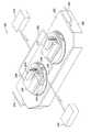
도 3은 덮개(202), 하우징들(204) 및 전력 소스들(214)을 가지는 탠덤형 프로세싱 챔버(106)의 부분적인 단면도를 도시한다. 하우징들(204)의 각각은 본체(200) 내에 규정된 2개의 프로세싱 영역들(300) 위에 각각 배치된 2개의 UV 램프 전구들(302) 중 각각의 하나의 전구를 커버한다. 프로세싱 영역들(300)의 각각은 프로세싱 영역들(300) 내에서 기판(308)을 지지하기 위한, 기판 지지부(306)와 같은, 가열 기판 지지부를 포함한다. 기판 지지부들(306)은 세라믹 또는 알루미늄과 같은 금속으로 만들어질 수 있다. 바람직하게, 기판 지지부들(306)은, 본체(200)의 바닥을 통해서 연장하고 구동 시스템들(312)에 의해서 동작되어 프로세싱 영역들(300)의 기판 지지부들(306)을 UV 램프 전구들(302)을 향해서 그리고 그로부터 멀리 이동시키는, 스템들(310)에 커플링된다. 구동 시스템들(312)은 또한 기판 조사 균일성을 더 강화하기 위해서 경화 동안에 기판 지지부들(306)을 회전 및/또는 병진운동시킬 수 있다. 기판 지지부들(306)의 조정가능한 위치결정은, 초점 거리와 같은 광 운반 시스템 설계 고려사항들(considerations)의 본질에 따라서 기판(308) 상에서의 입사 UV 복사조도(irradiance) 레벨들의 잠재적인 미세 조율(tuning) 뿐만 아니라 휘발성 경화 부산물 및 퍼지 및 세정 가스 유동 패턴들 및 체류 시간들을 제어할 수 있게 한다.Figure 3 shows a partial cross-sectional view of a tandem-shaped
일반적으로, 수은 마이크로파 아아크 램프들, 펄스형 제논 플래시 램프들 또는 고효율의 UV 발광 다이오드 어레이들과 같은 임의의 UV 소스가 이용될 수 있다. UV 램프 전구들(302)은 전력 소스들(214)에 의한 여기를 위한 제논(Xe) 또는 수은(Hg)과 같은 하나 또는 둘 이상의 가스들로 충진된 밀봉형 플라즈마 전구들이다. 바람직하게, 전력 소스들(214)은 하나 또는 둘 이상의 마그네트론들(미도시) 및 마그네트론들의 필라멘트들에 에너지를 공급하기 위한(energize) 하나 또는 둘 이상의 변압기들(transformers)(미도시)을 포함할 수 있는 마이크로파 발생기들이다. 킬로와트 마이크로파(MW) 전력 소스들을 가지는 하나의 실시예에서, 하우징들(204)의 각각은 전력 소스들(214)로부터 약 6000W 까지의 마이크로파 전력을 받아들이고 후속하여 전구들(302)의 각각으로부터 약 100W 까지의 UV 광을 생성하기 위해서 전력 소스들(214) 근처의 개구(215)를 포함한다. 또 다른 실시예에서, 전력 소스들(214)이 전극에 대해서 직류 전류(DC) 또는 펄스형 DC와 같은 회로망 및/또는 전류 공급부들에 해당하도록(represent), UV 램프 전구들(302)이 전극 또는 필라멘트를 내부에 포함할 수 있다.In general, any UV source such as mercury microwave arc lamps, pulsed xenon flash lamps or high efficiency UV light emitting diode arrays may be used.
몇몇 실시예들의 경우에, 전력 소스들(214)은 UV 램프 전구들(302) 내의 가스들을 여기할 수 있는 무선 주파수(RF) 에너지 소스들을 포함할 수 있다. 전구 의 RF 여기의 구성은 용량형 또는 유도형일 수 있다. 유도 결합형 플라즈마(ICP) 전구는 용량 결합형 방전에 의한 것보다 더 조밀한(denser) 플라즈마의 발생에 의해서 전구 광도(brilliancy)를 효율적으로 증대시키는데 이용될 수 있다. 또한, ICP 램프는 전극 열화(degradation)로 인한 UV 출력의 열화를 없애고, 강화된 시스템 생산성을 위한 더 긴-수명의 전구를 초래한다. 전력 소스들(214)이 RF 에너지 소스들이 되는 것의 이점들에는 효율 증가가 포함된다.In some embodiments, the
바람직하게, 전구들(302)은 170 nm 내지 400 nm 파장의 넓은 대역에 걸쳐서 광을 발산한다. 본원 발명의 하나의 실시예에서, 전구들(302)은 185 nm 내지 255 nm 파장으로 광을 발산한다. 전구들(302) 내에서 이용하기 위해서 선택된 가스들이 발산되는 파장들을 결정할 수 있다. UV 램프 전구들(302)로부터 발산된 UV 광이 덮개(202)의 개구들에 배치된 윈도우들(314)을 통과함으로써 프로세싱 영역들(300)로 들어간다. 바람직하게, 윈도우들(314)은 OH가 없는 합성 석영 유리로 만들어지고 균열(cracking)없이 진공을 유지하기 위한 충분한 두께를 가진다. 또한, 바람직하게, 윈도우들(314)은 대략 150 nm 까지(down to)의 UV 광을 전달하는 용융 실리카이다. 덮개(202)가 본체(200)를 밀봉하고 윈도우들(314)이 덮개(202)에 대해서 밀봉되기 때문에, 프로세싱 영역들(300)은 대략 1 Torr 내지 대략 650 Torr의 압력들을 유지할 수 있는 용적들을 제공한다. 프로세싱 또는 세정 가스들이 2개의 유입구 통로들(316)의 각각의 하나의 통로를 통해서 프로세싱 영역들(300)로 들어간다. 그런 다음에, 프로세싱 또는 세정 가스들이 공동 배출구 포트(318)를 통해서 프로세싱 영역들(300)을 빠져나간다. 추가적으로, 하우징들(204)의 내부로 공급되는 냉각 공기가 전구들(302)을 지나서 순환하지만, 윈도우들(314)에 의해서 프로세싱 영역들(300)로부터 격리된다.Preferably, the
하우징들(204)은 2색성(dichroic) 필름으로 코팅된 주조 석영 라이닝(cast quartz lining; 304)에 의해서 규정된 내부 포물선형 표면을 포함할 수 있다. 석영 라이닝들(304)은 UV 램프 전구들(302)로부터 발산된 UV 광을 반사시키고 그리고 석영 라이닝들(304)에 의해서 프로세싱 영역들(300)내로 지향되는 UV 광의 패턴에 기초하여 챔버 세정 프로세스들 뿐만 아니라 경화 프로세스들에 적합하도록 성형된다. 석영 라이닝들(304)은 내부 포물선형 표면의 형상을 이동시키고 변경함으로써 각각의 프로세스 또는 작업(task)에 더 적합하도록 조정할 수 있다. 추가적으로, 석영 라이닝들(304)은 2색성 필름에 기인하여 전구들(302)에 의해서 발산되는 자외선 광을 반사시킬 수 있고 적외선 광을 전달할 수 있다. 일반적으로, 2색성 필름은 교호적인(alternating) 높은 굴절률 및 낮은 굴절률을 가지는 다양한 유전체 재료들로 이루어진 주기적인(periodic) 다층 필름을 구성한다. 코팅이 비-금속성이기 때문에, 주조 석영 라이닝들(304)의 후방측부(backside) 상으로 하향 입사되는 전력 소스들(214)로부터의 마이크로파 복사선은 변조된(modulated) 층들과 크게 상호작용하지 않거나 또는 변조된 층들에 의해서 흡수되지 않으며, 전구들(302)에서 가스들을 이온화하기 위해서 용이하게 전달된다.The
기판(308) 상에 증착된 유전체 필름들의 후처리 경화를 실시하기 위해서, 기판들이 프로세싱 영역(300) 내로 옮겨진다. 필름들은, 예를 들어, 필름 내에 실리콘 백본(backbone) 구조 및 탄소를 포함하는 포로겐을 가지는 저-k 유전체 필름들일 수 있다. 필름 내의 실리콘 백본 구조 및 탄소가 종종 포로겐으로 지칭된다. UV 노출 후에, 탄소 결합들이 파괴되고 그리고 탄소가 필름으로부터 가스배출되어, 실리콘 백본을 남기고 다공도를 높이며, 그러한 높은 다공도는 k 값을 줄이고 필름의 전류 용량(current carrying capacity)을 감소시킨다.Substrates are transferred into the
통상적인 시스템들에서, 교차-유동하는(cross-flow) 불균일 가스 유동 프로파일은 기판의 경화 및 가스배출 동안에 챔버를 퍼지(purge)한다. 퍼지 가스는, 기판과 윈도우 사이에서, 챔버의 일 측부로부터 대향 측부로 유동하며, 그에 따라 필름을 빠져나오는 임의의 잔류물이 윈도우 상에 또는 챔버의 임의의 개소 상에 응축될 수 있기 전에 제거된다(carried away). 유동 프로파일의 제어되지 않은 불균일성으로 인해서, 기판 프로세싱 또한 불균일하게 될 것이고 기판에 걸친 온도 구배를 초래할 것이다. 그러나, 45 nm 범위의 필름들의 결과적인 불균일성이 용인 가능할 수 있지만, 차세대의 20-28 nm 필름들에서는 용인 가능하지 않을 것이다.In typical systems, a cross-flow uneven gas flow profile purges the chamber during curing and degassing of the substrate. The purge gas flows between the substrate and the window, from one side of the chamber to the opposite side, so that any residue exiting the film is removed before it can condense on the window or on any portion of the chamber lt; / RTI > Due to the uncontrolled non-uniformity of the flow profile, substrate processing will also be non-uniform and will result in a temperature gradient across the substrate. However, the resulting non-uniformity of films in the 45 nm range may be acceptable, but will not be acceptable for the next generation of 20-28 nm films.
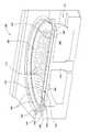
본원 발명의 실시예들은, UV 챔버, 램프 가열형 챔버, 또는 기판(308) 상에서 직접적으로 또는 기판(308) 위에서, 필름을 프로세싱하기 위해서 또는 반응을 촉진하기 위해서 "광" 에너지가 이용되는 다른 챔버 내에서 프로세싱되는 기판(308)에 걸친 특정 가스 유동 프로파일 분배를 가능하게 하는 하드웨어의 설계를 포함한다. 본원 발명의 여러 가지 실시예들이 도 4-5b와 관련하여 설명될 것이다. 도 4는 가스 유동 프로파일 균일성을 개선하기 위해서 그리고 프로세싱 동안에 기판 처리량을 증가시키기 위해서 본원 발명의 실시예들을 포함하는 프로세싱 챔버들(400) 중 하나의 부분의 개략적인 등각 단면도를 도시한다. 도 5a는 윈도우 조립체가 없는 도 4의 프로세싱 챔버(400)의 개략적인 등각 단면도이다. 도 5b는 도 5a에 도시된 샤워헤드의 단면의 근접도이다.Embodiments of the present invention may be used to process a film directly or on a
프로세싱 챔버(400)의 부분은, 프로세싱 챔버를 통한 가스 유동 프로파일의 제어를 가능하게 하는 여러 가지 하드웨어 설계들을 도시한다. 윈도우 조립체가 프로세싱 챔버(400) 내에 위치되어 UV 진공 윈도우(412)를 유지한다. 윈도우 조립체는, 본체(200)의 부분 상에 놓이고 진공 윈도우(412)를 지지하는 진공 윈도우 클램프(410)를 포함하고, UV 광이 UV 램프들(302)로부터 진공 윈도우(412)를 통과할 수 있고, 진공 윈도우는 본체(200) 위의 덮개 조립체의 일부이다. 진공 윈도우(412)는 UV 램프들(302)과 같은 UV 복사선 소스와 기판 지지부(306) 사이에 위치된다. UV 복사선 소스(302)는 기판 지지부(306)로부터 이격되고 자외선 복사선을 생성하여 기판 지지부(306) 상에 위치된 기판(308)으로 전달하도록 구성된다.Portions of the
투과성 샤워헤드(414)가 프로세싱 영역(300) 내에 그리고 진공 윈도우(412)와 기판 지지부(306)와 같은 기판 지지부 사이에 위치된다. 투과성 샤워헤드는 진공 윈도우(412)와 투과성 샤워헤드(414) 사이에 상부 프로세싱 영역(320)을 규정하고 그리고 투과성 샤워헤드(414)와 기판 지지부(306)(도 5a)와 같은 기판 지지부 사이에 하부 프로세싱 영역(322)을 추가적으로 규정한다. 투과성 샤워헤드(414)는 또한 상부 프로세싱 영역(320)과 하부 프로세싱 영역(322) 사이에 하나 또는 둘 이상의 통로들(416)을 가진다. 통로들(416)은 종종 "반투과성(frosted)" 표면으로 지칭되는 거친 표면(418)을 가질 수 있고, 그에 따라 통로들(416)이 완전히(perfectly) 투과적이지 않으며, 만약 통로들이 완전히 투과적이라면 기판(308) 상에서 음영부들(shadows)을 잠재적으로 유발할 수 있고 그리고 필름의 적절한 경화를 손상시킬 수 있다. 반투과성일 수 있는 통로들(416)이 UV 광을 확산시키고, 그에 따라 프로세싱 동안에 기판(308) 상에 광 패턴이 존재하지 않는다.A
투과성 샤워헤드(414)가 제 2 윈도우를 형성하고, 그러한 제 2 윈도우를 통해서 기판(308)에 도달하기 위해 UV 광이 통과할 수 있다. 제 2 윈도우로서, 샤워헤드(414)는 기판(308) 상의 필름을 경화시키기 위해서 요구되는 광의 파장들에 대해서 투과적일 필요가 있다. 투과성 샤워헤드는 석영 또는 사파이어와 같은 여러 가지 투과성 재료들로 형성될 수 있다. 통로들(416)은, 프로세싱 영역(300) 내에 피팅(fit)되도록 투과성 샤워헤드(414)를 형성하고 성형하기 위한 석영 피스(piece)를 통해서 홀들을 드릴가공함으로써 형성될 수 있다. 석영 피스의 표면이 불꽃 연마될(flame polished) 수 있는 반면, 드릴가공된 홀들은 거친 표면(418)을 형성하기 위해 에칭될 수 있다. 기판 표면에 걸친 원하는 유동 특성들을 달성하기 위해서, 통로들(416)의 크기 및 밀도가 균일하거나 불균일할 수 있다. 통로들(416)은 기판(308)에 걸친 각 방사상 지역당 유동이 균일한 균일 유동 프로파일을 가질 수 있거나 또는 가스 유동이 기판(308)의 중심 또는 엣지에 대해서 차별적일 수 있는, 즉 가스 유동이 차별적인 유동 프로파일을 가질 수 있는 불균일 유동 프로파일을 가질 수 있다.The
대역 통과 필터를 가지도록 그리고 원하는 파장들의 투과(transmission)를 개선하도록, 투과성 샤워헤드(414) 및 진공 윈도우(412)가 코팅될 수 있다. 예를 들어, 반사방지 코팅(ARC)이 투과성 샤워헤드(414) 및 진공 윈도우(412) 상에 증착되어 원하는 파장들의 투과 효율을 개선할 수 있다. IR을 반사시키고 UV가 통과하도록 허용하는 반사 코팅 또는 UV을 반사시키고 IR가 통과하도록 허용하는 2색성 코팅이 또한 투과성 샤워헤드(414) 및 진공 윈도우(412) 표면들에 도포될 수 있다. 코팅은 PVD, CVD 또는 다른 적절한 증착 기술들에 의해서 형성될 수 있다. 코팅들은, 투과성 샤워헤드(414) 및 진공 윈도우(412)를 통한 기판(308)으로의 광 투과를 도울 수 있는 원하는 필름 투과도 및 굴절률을 가지는 무기(inorganic) 필름 층을 포함할 수 있다. 하나의 실시예에서, 코팅들은 티타늄 산화물(Ti02) 층, 주석 산화물 층(Sn02), 실리콘 산화물(Si02) 또는 이들의 조합을 포함할 수 있고, 진공 윈도우(412) 및 투과성 샤워헤드(414)의 표면들 상에 형성된다.A
또 다른 실시예에서, ARC 코팅이 투과성 샤워헤드(414) 및 진공 윈도우(412)의 표면들 상에 형성된 하나 또는 둘 이상의 층들을 가지는 복합 층(composite layer)일 수 있다. 하나의 실시예에서, ARC 코팅은, 투과성 샤워헤드(414) 및 진공 윈도우(412)의 표면들 상에 형성된, 제 2 층 상에 형성된 제 1 층을 포함하는 필름 적층체(stack)일 수 있다. 하나의 실시예에서, 제 1 층이 실리콘 산화물 층(Si02)일 수 있고 제 2 층이 티타늄 산화물(Ti02) 층 또는 주석 산화물 층(Sn02)일 수 있거나 그 반대일 수 있다. 또 다른 실시예에서, ARC 층은 반복되는 실리콘 산화물(Si02) 및 티타늄 산화물(Ti02) 층들을 포함하는 필름 적층체를 포함할 수 있다.In another embodiment, the ARC coating may be a composite layer having one or more layers formed on the surfaces of the
하나 또는 둘 이상의 가스 분배 링 통로들(426)을 가지는 가스 분배 링(420)이 프로세싱 영역(300) 내에 배치된다. 하나 또는 둘 이상의 가스 분배 링 통로들(426)이 가스 분배 링 내측 채널(424)을 상부 프로세싱 영역(320)과 커플링시켜, 내측 채널(424)과 투과성 샤워헤드(414) 위쪽의 상부 프로세싱 영역(320) 사이의 가스 유동 경로를 형성한다. 가스 배출구 링(430)이 가스 분배 링(420) 아래에 위치되고 그리고 프로세싱 영역(300) 내의 투과성 샤워헤드(414) 아래에 적어도 부분적으로 있을 수 있다. 가스 배출구 링(430)은 또한 가스 배출구 링 내측 채널(434)과 하부 프로세싱 영역(322)을 커플링시키는 하나 또는 둘 이상의 배출구 통로들(436)을 가지며, 하부 프로세싱 영역(322)과 가스 배출구 내측 채널(434) 사이의 가스 유동 경로를 형성한다. 가스 배출구 링(430)의 하나 또는 둘 이상의 가스 배출구 통로들(436)이 투과성 샤워헤드(414) 아래에 적어도 부분적으로 배치된다.A
도 6은 가스 유동 경로를 도시한 도 5a 내의 프로세싱 챔버의 개략적인 단면도를 나타낸다. 퍼지 가스 또는 다른 유형들의 가스들이 진공 윈도우(412)와 투과성 샤워헤드(414) 사이의 상부 프로세싱 영역(320) 내로, 투과성 샤워헤드(414)를 통해서, 그리고 투과성 샤워헤드(414)로부터 기판을 향해서 아래쪽으로 주입될 수 있다. 기판(308)을 향한 하향 유동을 균등하게 만들기 위한(even out) 배압이 형성되도록 통로들(416, 426, 436)의 크기 및 가스 유량들이 조정될 수 있다. 가스 유동은 위로부터 기판 상으로 워싱하고(wash), 동심적으로 펼쳐지며(spread out), 그리고 가스 배출구 통로들(436)을 통해서 펌프(610)로 하부 프로세싱 영역(322)을 빠져나간다.Figure 6 shows a schematic cross-sectional view of the processing chamber in Figure 5a showing the gas flow path. Purge gas or other types of gases may be introduced into the
화살표들(605)은 가스 분배 링(420)으로부터, 투과성 샤워헤드(414)를 통해서, 기판(308)을 또한 상부에 가질 수 있는 기판 지지부(306) 상으로, 가스 배출구 링(430)을 통해서, 그리고 챔버(400)를 빠져나가는 가스 유동 경로를 나타낸다. 통로들(416, 426, 436)의 밀도 및 크기는 원하는 대로 가스 유동 속도를 증가 또는 감소시키도록 조정될 수 있다. 하나의 실시예에서, 통로들(416, 426, 436)의 밀도 및 크기는 기판(308)에 걸친 균일한 유동 프로파일을 제공한다. 가스 분배 링(420)과 같은 하드웨어는, 투과성 샤워헤드(414) 위의 상부 프로세싱 영역(320)으로 들어가기에 앞서서 가스들을 균일하게 분배시키기 위한 충분한 압력 강하를 제공한다. 그런 다음에, 샤워헤드(414)의 통로들(416)을 통한 높은 유동 저항으로 인해서, 가스들이 투과성 샤워헤드(414) 위의 상부 프로세싱 영역(320)을 균일하게 충진할 수 있다. 가스 유동이 기판으로 진행되고 그런 다음에 가스 배출구 링(430)을 통해서 펌프(610)로 균일하게 펌핑 아웃(pumped out)된다.The
샤워헤드(414)의 통로들(416)의 패턴에 따라서, 유동이 균일할 수 있거나(기판 면적에 비례) 또는 중심이나 엣지를 향해서 차별적일 수 있다. 따라서, 원하는 균일한 또는 불균일한 분배를 제공하기 위해 가스 유동 프로파일이 기판(308)에 걸쳐서 제어될 수 있다. 추가적으로, 기판(308)에 걸친 온도 프로파일이 또한 균일하게 또는 불균일하게 제어될 수 있다. 따라서, 본원 발명의 실시예들은 기판에 걸친 균일한 가스 유동 및 온도 프로파일들을 생성할 수 있는 능력 뿐만 아니라, 원하는 불균일한 가스 및 온도 프로파일을 생성 및 제어할 수 있는 능력을 제공한다.Depending on the pattern of the
본원 발명의 몇몇 실시예들에서, 가스 조성물은 챔버 퍼지를 위한 퍼지 가스들을 포함할 수 있다. 그러한 가스들은 아르곤(Ar), 헬륨(He) 및 질소(N2) 등과 같은 불활성 가스 종 또는 비-반응성 가스들을 포함할 수 있다. 또 다른 실시예에서, 가스 조성물은 프로세싱 챔버 및 챔버 내의 구성요소들을 세정하기 위한 세정 가스들을 포함할 수 있다. 세정 가스들은 오존, Ar, He 또는 이들의 조합을 포함할 수 있다. 본원 발명의 실시예들은 세정 가스가 오존일 때 세정 프로세스를 개선하는데 특히 도움이 된다. 오존이 프로세싱 영역으로부터 원격적으로 발생될 수 있거나 또는 챔버 내로 오존을 도입하는 것이 오존을 생성하기 위해서 자외선 광으로 산소를 활성화시키는 것을 포함할 수 있다. 가스 공급부(600)가 오존 발생 소스를 프로세싱 영역(300)에 커플링시킬 수 있다. 오존을 이용할 때, 챔버의 용적이 작을수록 세정 효율이 개선될 수 있다. 증착된 잔류물들과 반응하여 그 잔류물들을 제거하기 위해, 프로세싱 영역으로 공급된 열 및 UV 광이 오존을 산소 라디칼들로 분해할 수 있다.In some embodiments of the invention, the gas composition may comprise purge gases for chamber purging. Such gases may include inert gas species such as argon (Ar), helium (He) and nitrogen (N2 ), or non-reactive gases. In another embodiment, the gas composition may comprise cleaning gases for cleaning the processing chamber and components within the chamber. The cleaning gases may include ozone, Ar, He, or a combination thereof. Embodiments of the present invention are particularly useful in improving the cleaning process when the cleaning gas is ozone. Ozone can be generated remotely from the processing region, or introducing ozone into the chamber can include activating oxygen with ultraviolet light to generate ozone. A
UV 램프(302)가 턴 온(turn on)될 때, 램프로부터 나오는 적외선 광으로 인해서 진공 윈도우(412) 및 투과성 샤워헤드(414) 모두가 가열된다. 투과성 샤워헤드(414)는 UV 광에 대해서 투과적일 수 있으나 IR 광의 일부를 흡수할 수 있고, 따라서, 오존이 상부 프로세싱 영역(320)에서 분해되고 그런 다음에 세정을 위해서 하부 프로세싱 영역(322) 내로 하향 이동하기 위해, 가열된 채널을 2개의 윈도우들 사이에 생성한다. 투과성 샤워헤드(414)에 의해서 흡수된 IR 광은 가스 분배 링(420)으로부터 상부 프로세싱 영역(320) 내로 주입된 오존과 상호작용하여 오존이 분해되도록 야기하는 온도 구배를 생성한다. 오존 분해량은, 샤워헤드(414)와 가스 분배 링(420)과 같이 상부 프로세싱 영역(320)을 둘러싸는 구성요소들의 표면적과 온도에 비례할 수 있다. 가열되는 구성요소들의 표면적을 증가시킴으로써, 오존을 반응성 산소 라디칼들로 분해하기 위해서 더 적은 에너지가 필요할 수 있고, 세정 효율들을 개선할 수 있다. 추가적으로, UV 광이 오존을 O2 및 라디칼 산소로 분해하게 될 기판(308)으로 오존이 균일하게 운반될 수 있고, O2 및 라디칼 산소는 기판(308) 상의 유기 필름 또는 재료를 에칭하기 위해서 이용될 수 있다.When the
도 6에 도시된 바와 같이, 진공 윈도우 클램프(410), 진공 윈도우(412), 및 가스 분배 링(420)과 같은 프로세싱 챔버 내의 구성요소들을 가열하기 위해서 또 다른 히터(630)가 이용될 수 있다. 이러한 하드웨어 구성요소들을 가열하는 것은 오존 디제너레이션(ozone degeneration)의 효율을 개선할 수 있고 그리고 구성요소들 상의 포로겐의 증착을 감소시킬 수 있다. 이러한 구성요소들의 방사율(emissivity)을 증가시키기 위해 가스 분배 링(420), 가스 배출구 링(430), 및 진공 윈도우 클램프(410)가 양극처리된(anodized) 알루미늄으로 만들어질 수 있다. 그런 다음에, 구성요소들은 더 많은 열을 흡수할 수 있어서, 구성요소들의 온도를 높이고, 구성요소들 상의 잔류물 증착량을 감소시키며, 세정 시간들의 감소, 개선된 처리량, 및 입자 성능(particle performance)을 초래할 수 있다. 추가적으로, 또한 포로겐이 배기 포트(317)에서 수집되는 것을 방지 또는 감소시키기 위해서 열이 배기 포트(317)에 제공될 수 있다.6, another
가스 공급부(600)가 가스 분배 링(420)에 커플링되어, 챔버(400)에서 실시될 수 있는 증착, 형성, 처리, 퍼지, 및 세정 프로세스들을 위한 여러 가지 가스들을 제공한다. 또 다른 실시예에서, 원한다면, 원격 플라즈마 소스(RPS)가 또한 가스 분배 링(420)과 커플링되어 플라즈마 에너지 공급형 종(plasma energized species)을 프로세싱 영역 내로 제공할 수 있다. 챔버로부터 가스 화합물들을 제거하기 위해서, 가스 펌프(610)가 가스 배출구 링(430)과 커플링된다. 추가적으로, 하부 프로세싱 영역(322)의 가스들을 포함하여, 기판 및 주변 지역들을 가열하기 위해서, 히터(620)가 기판 지지부(306)와 커플링된다.A
도 7은 도 6에 도시된 바와 같은 가스 유동 경로 및 프로세싱 챔버의 부분의 근접 등각 단면도이다. 가스 분배 링(420) 및 가스 배출구 링(430)은 여러 가지 구성요소들을 포함할 수 있다. 가스 분배 링(420)은 베이스 분배 링(421) 및 가스 유입구 링(423)을 포함할 수 있다. 베이스 분배 링(421)은 하나 또는 둘 이상의 가스 분배 링 통로들(426)을 규정할 수 있다. 가스 유입구 링(423)은 베이스 분배 링(421)과 커플링될 수 있고, 이들은 함께 가스 분배 링 내측 채널(424)을 규정할 수 있다. 가스 유입구 링(423)은 또한 하나 또는 둘 이상의 가스 유입구들(425)을 포함할 수 있고, 그러한 가스 유입구들을 통해서 가스가 가스 분배 링 내측 채널(424)로 들어갈 수 있다. 가스 종 및 혼합물들을 가스 분배 링(420)에 제공하기 위해서 가스 공급부(600)가 가스 유입구들(425)에 커플링된다.Figure 7 is a close-up isometric cross-sectional view of the gas flow path and portion of the processing chamber as shown in Figure 6; The
가스 배출구 링(430)은 베이스 배출구 링(431) 및 가스 펌핑 링(433)을 포함할 수 있다. 가스 펌핑 링(433)은 하나 또는 둘 이상의 가스 배출구 통로들(436)을 규정할 수 있고 투과성 샤워헤드(414)를 지지할 수 있다. 베이스 배출구 링(431)이 가스 펌핑 링(433)과 커플링되어 가스 배출구 링(430)을 형성한다. 베이스 배출구 링(431) 및 가스 펌핑 링(433)은 가스 배출구 링 내측 채널(434)을 함께 규정할 수 있다. 가스 배출구 링(430)(도 6 참조)의 적어도 하나의 가스 배출구(438)는 가스가 가스 배출구 링(430)을 빠져나가도록 배기 포트(317)와 정렬될 수 있다.The
도 7에 도시되고 화살표들(605)에 의해 표시된 바와 같이, 가스는 가스 유입구(425)에 들어가고 가스 분배 링 내측 채널(424)을 통해서 가스 배출구 링(430)의 통로들(426) 외부로 유동할 수 있다. 가스는 투과성 샤워헤드(414) 위쪽의 용적 예를 들어, 상부 프로세싱 영역(320)을 충진하고, 샤워헤드 통로들(416)을 통해서 유동한다. 그런 다음에, 가스는 동심적으로 그리고 방사상으로 기판(308)을 가로질러 가스 배출구 통로들(436)로 유동한다. 이어서, 가스는 하부 프로세싱 영역(322)으로부터 방출되고, 가스 배출구 링 내측 채널(434)로 들어가고, 내측 채널(434)을 통해서 유동하며, 그리고 가스 배기 포트(317) 내로 그리고 펌프(610)로 가스 배출구(438)를 빠져나간다.The gas enters the
본원 발명의 실시예들에 의해서 제공된 동심적인 유동 프로파일은 또한, 예를 들어 기판 엣지 저온 프로세스(cold process) 또는 엣지 고온 프로세스(hot process)가 요구될 수 있는 경우에, 기판(308) 상의 온도 프로파일을 변경하기 위해서 압력, 가스 조성물들, 가스 혼합물들 등의 조정들을 허용할 수 있다. 통상적인 설계들은, 기판 표면에 걸친 온도 프로파일들의 생성 및 제어를 위한 이러한 변수들의 조정가능성을 허용하지 않았다. 예를 들어, 본원 발명의 몇몇 실시예들에서, 압력의 변경들 및 더 많은 아르곤 또는 더 많은 헬륨이 온도 프로파일을 조정하기 위해 이용될 수 있다. 헬륨은 열 전달에 있어서 더 효율적이고, 그리고 압력은 가스들의 체류 시간을 변화시킬 수 있다. 투과성 샤워헤드를 통한 유동 분배를 위한 통로 크기와 함께 이러한 프로세스 변수들을 조정하는 것은 기판(308) 상의 원하는 위치들에서 기판에 걸친 온도 프로파일을 균일해지도록 또는 불균일해지도록 제어하는 것에 기여할 수 있고, 그에 따라 기판(308) 및 기판 상의 필름들을 차별적으로 처리하는 것에 기여할 수 있다. 몇몇 실시예들에서, 가스들이 프로세싱 챔버(400) 내의 상이한 영역들에서 주입될 수 있다.The concentric flow profile provided by embodiments of the present invention can also be used to determine the temperature profile on the
UV 경화는, 필름 보수 및 필름의 변형 에너지를 증대시키기 위한 필름의 수소 결합들의 파괴를 위한 것과 같은 여러 가지 용도들을 가질 수 있다. 또한, 프로세싱 챔버(400)는, 기판(308) 상에 필름들을 형성하기 위해서 UV 활성화된 가스 종을 프로세싱 영역(300) 내로 주입하기 위해서 이용될 수 있다. 특정 가스들이 기판(308) 위에서 혼합될 수 있고, 여기에서 UV 광을 이용하고 "드롭-온(drop-on)" 증착 프로세스가 가능하게 하여 기상에서(in the gaseous phase) 반응이 활성화될 수 있다. 또 다른 실시예에서, 기판(308) 상에 필름을 형성하기 위한 촉매로서 이용될 수 있도록 가스들이 UV 광과 반응할 수 있다. 따라서, 가스 공급부(600)는 또한, 필름 형성을 위해서 UV 광으로 개시될 수 있는 비-반응성 가스들 및 전구체들을 포함할 수 있다. 몇몇 실시예들에서, 필름이 상부에 증착되는 것을 방지하기 위해서, 윈도우(412) 및 샤워헤드(414)가 냉각될 필요가 있을 수 있거나 또는 적어도 가열되지 않을 필요가 있을 수 있다. 그러나, 임의의 그러한 필름 증착물들을 윈도우(412) 및 샤워헤드(414)로부터 제거하기 위해서 오존 세정 프로세스가 개시될 수 있다. 추가적으로, 단일(mono)-층 또는 다중-층 필름을 기판 상에 생성하기 위해서 가스들이 균일하게 옮겨질 수 있다. 그런 다음에, 원하는 대로 증착 층들을 더 형성하기 위해서, UV 에너지가 기판(308) 상의 반응을 활성화시키도록 이용될 수 있다.UV curing may have several uses, such as for film repair and destruction of the hydrogen bonds of the film to increase the strain energy of the film. In addition, the
본원 발명의 실시예들은 기판의 온도 균일성을 2-3배 만큼 개선하고 그리고 진공 윈도우가 더 효과적으로 세정된다. 이러한 시스템의 처리량이 증대되는데, 이는 그 시스템이 세정 및 경화 프로세스들 모두의 효율이 더 높아질 수 있게 하기 때문이다. 몇몇 경우들에서, 개선된 경화 시간이 10-15% 만큼 감소되는데, 이는 기판(308)의 더 균일한 온도들의 결과인 것으로 여겨지며, 챔버 내에서 또는 기판(308) 상에서 저온 점(spot)을 가지지 않고, 증착된 잔류물들의 누적에 의해서 유발되는 윈도우 표면에 걸친 상이한 광 세기들을 감소시키기 위해서 윈도우를 더 청정하게 유지한다. 추가적으로, 프로세싱 챔버를 통해서 유동시킬 필요가 있는 가스의 양이 감소될 수 있는데, 이는 가스의 더 효과적인 이용 때문이다.Embodiments of the present invention improve the temperature uniformity of the substrate by 2-3 times and the vacuum window is cleaned more effectively. The throughput of such a system is increased because it allows the efficiency of both the cleaning and curing processes to be higher. In some cases, the improved cure time is reduced by 10-15%, which is believed to be the result of more uniform temperatures of the
전술한 내용들이 본원 발명의 실시예들에 관한 것이지만, 본원 발명의 다른 그리고 추가적인 실시예들이 본원 발명의 기본적인 범위로부터 벗어나지 않고 안출될 수 있다.While the foregoing is directed to embodiments of the present invention, other and further embodiments of the invention may be devised without departing from the basic scope thereof.
Claims (15)
Translated fromKorean프로세싱 영역을 규정하는 자외선 프로세싱 챔버;
상기 프로세싱 영역 내에서 기판을 지지하기 위한 기판 지지부;
상기 기판 지지부로부터 이격되고 그리고 자외선(UV) 복사선을 발생시키고 상기 기판 지지부 상에 위치된 기판으로 전달하도록 구성된 자외선 복사선 소스;
상기 UV 복사선 소스와 상기 기판 지지부 사이에 배치된 윈도우;
상기 윈도우와 상기 기판 지지부 사이의 프로세싱 영역 내에 배치되고 상부 프로세싱 영역 및 하부 프로세싱 영역을 규정하는 투과성 샤워헤드 ― 상기 상부 프로세싱 영역은 상기 윈도우와 상기 투과성 샤워헤드 사이에 위치되고 그리고 상기 하부 프로세싱 영역은 상기 투과성 샤워헤드와 상기 기판 지지부 사이에 위치되고, 상기 투과성 샤워헤드는 상기 상부 프로세싱 영역과 상기 하부 프로세싱 영역 사이에 하나 또는 둘 이상의 투과성 샤워헤드 통로들을 가짐 ―;
가스 분배 링 내의 가스 분배 링 내측 채널과 상기 상부 프로세싱 영역 사이에 하나 또는 둘 이상의 가스 분배 링 통로들을 가지는 가스 분배 링; 및
상기 가스 분배 링 아래에 위치된 가스 배출구 링을 포함하고,
상기 가스 배출구 링은 상기 가스 배출구 링 내의 가스 배출구 링 내측 채널과 상기 하부 프로세싱 영역 사이에 하나 또는 둘 이상의 가스 배출구 통로들을 가지고, 상기 가스 배출구 링은 상기 가스 분배 링과 분리되어 있는, 프로세싱 도구.As a processing tool:
An ultraviolet processing chamber defining a processing region;
A substrate support for supporting a substrate within the processing region;
An ultraviolet radiation source spaced from the substrate support and configured to generate ultraviolet (UV) radiation and deliver the substrate to a substrate positioned on the substrate support;
A window disposed between the UV radiation source and the substrate support;
A transmissive showerhead disposed within a processing region between the window and the substrate support and defining an upper processing region and a lower processing region, the upper processing region being located between the window and the transmissive showerhead, The transmissive shower head having one or more transmissive showerhead passages between the upper processing area and the lower processing area;
A gas distribution ring having one or more gas distribution ring passages between the gas distribution ring inner channel and the upper processing region in the gas distribution ring; And
A gas outlet ring located below said gas distribution ring,
Wherein the gas outlet ring has one or more gas outlet passages between the gas outlet ring inner channel and the lower processing area in the gas outlet ring, the gas outlet ring being separate from the gas distribution ring.
상기 하나 또는 둘 이상의 가스 배출구 통로들은 상기 투과성 샤워헤드 아래에 적어도 부분적으로 배치되는, 프로세싱 도구.The method according to claim 1,
Wherein the one or more gas outlet passages are disposed at least partially below the transmissive showerhead.
상기 가스 분배 링은:
상기 하나 또는 둘 이상의 가스 분배 링 통로들을 규정하는 베이스 분배 링; 및
상기 베이스 분배 링과 커플링된 가스 유입구 링을 더 포함하고,
상기 베이스 분배 링 및 상기 가스 유입구 링은 상기 가스 분배 링 내측 채널을 함께 규정하고, 상기 가스 유입구 링은 가스가 상기 가스 분배 링 내측 채널에 들어가기 위한 하나 또는 둘 이상의 가스 유입구들을 더 포함하는, 프로세싱 도구.The method according to claim 1,
The gas distribution ring comprising:
A base distribution ring defining said one or more gas distribution ring passages; And
Further comprising a gas inlet ring coupled with the base distribution ring,
Wherein the base distribution ring and the gas inlet ring together define an inner channel of the gas distribution ring and wherein the gas inlet ring further comprises one or more gas inlets for the gas to enter the inner channel of the gas distribution ring, .
상기 가스 배출구 링은:
상기 하나 또는 둘 이상의 가스 배출구 통로들을 규정하는 가스 펌핑 링; 및
상기 가스 펌핑 링과 커플링된 베이스 배출구 링을 더 포함하고,
상기 가스 펌핑 링 및 상기 베이스 배출구 링은 가스 배출구 링 내측 채널을 함께 규정하고, 상기 베이스 배출구 링은 가스가 상기 가스 배출구 링을 빠져나가기 위한 적어도 하나의 가스 배출구를 더 포함하는, 프로세싱 도구.The method according to claim 1,
Said gas outlet ring comprising:
A gas pumping ring defining said one or more gas outlet passages; And
Further comprising a base outlet ring coupled with the gas pumping ring,
Wherein the gas pumping ring and the base outlet ring together define a gas outlet ring inner channel and wherein the base outlet ring further comprises at least one gas outlet for gas to exit the gas outlet ring.
상기 하나 또는 둘 이상의 투과성 샤워헤드 통로들은 균일한 유동 프로파일 ― 상기 기판에 걸친 각 방사상 구역당 가스 유동이 균일함 ―을 가지는, 프로세싱 도구.The method according to claim 1,
Wherein the one or more transmissive showerhead passages have a uniform flow profile - uniform gas flow per radial zone across the substrate.
상기 하나 또는 둘 이상의 투과성 샤워헤드 통로들은 차별적인 유동 프로파일 ― 각 방사상 구역당 가스 유동이 상기 기판의 중심 또는 엣지에 대해서 차별적임 ―을 가지는, 프로세싱 도구.The method according to claim 1,
Wherein the one or more permeable showerhead passages have differential flow profiles, wherein gas flow per radial zone is different for the center or edge of the substrate.
상기 가스 분배 링과 커플링되는 가스 공급부; 및 상기 가스 배출구 링과 커플링되는 가스 펌프를 더 포함하는,
프로세싱 도구.The method according to claim 1,
A gas supply coupled to the gas distribution ring; And a gas pump coupled to the gas outlet ring,
Processing tools.
상기 가스 펌핑 링은 상기 투과성 샤워헤드를 지지하는,
프로세싱 도구.5. The method of claim 4,
Wherein the gas pumping ring supports the permeable shower head,
Processing tools.
상기 프로세싱 영역으로부터 원격적으로 위치되는 오존 발생 소스; 및
상기 프로세싱 영역에 상기 오존 발생 소스를 커플링시키는 상기 가스 공급부
를 더 포함하는,
프로세싱 도구.8. The method of claim 7,
An ozone generating source remotely located from the processing region; And
Wherein the gas supply source for coupling the ozone generating source to the processing region
≪ / RTI >
Processing tools.
Applications Claiming Priority (3)
| Application Number | Priority Date | Filing Date | Title |
|---|---|---|---|
| US39471110P | 2010-10-19 | 2010-10-19 | |
| US61/394,711 | 2010-10-19 | ||
| PCT/US2011/054014WO2012054206A2 (en) | 2010-10-19 | 2011-09-29 | Quartz showerhead for nanocure uv chamber |
Publications (2)
| Publication Number | Publication Date |
|---|---|
| KR20130129943A KR20130129943A (en) | 2013-11-29 |
| KR101896607B1true KR101896607B1 (en) | 2018-09-07 |
Family
ID=45933035
Family Applications (1)
| Application Number | Title | Priority Date | Filing Date |
|---|---|---|---|
| KR1020137012575AExpired - Fee RelatedKR101896607B1 (en) | 2010-10-19 | 2011-09-29 | Quartz showerhead for nanocure uv chamber |
Country Status (6)
| Country | Link |
|---|---|
| US (1) | US8911553B2 (en) |
| JP (1) | JP5905476B2 (en) |
| KR (1) | KR101896607B1 (en) |
| CN (1) | CN103109357B (en) |
| TW (1) | TWI537417B (en) |
| WO (1) | WO2012054206A2 (en) |
Cited By (1)
| Publication number | Priority date | Publication date | Assignee | Title |
|---|---|---|---|---|
| WO2023287699A1 (en)* | 2021-07-12 | 2023-01-19 | Applied Materials, Inc. | Improved showerhead pumping geometry for precursor containment |
Families Citing this family (397)
| Publication number | Priority date | Publication date | Assignee | Title |
|---|---|---|---|---|
| US8673080B2 (en) | 2007-10-16 | 2014-03-18 | Novellus Systems, Inc. | Temperature controlled showerhead |
| US10378106B2 (en) | 2008-11-14 | 2019-08-13 | Asm Ip Holding B.V. | Method of forming insulation film by modified PEALD |
| US9394608B2 (en) | 2009-04-06 | 2016-07-19 | Asm America, Inc. | Semiconductor processing reactor and components thereof |
| US8802201B2 (en) | 2009-08-14 | 2014-08-12 | Asm America, Inc. | Systems and methods for thin-film deposition of metal oxides using excited nitrogen-oxygen species |
| US8481355B2 (en)* | 2009-12-15 | 2013-07-09 | Primestar Solar, Inc. | Modular system and process for continuous deposition of a thin film layer on a substrate |
| WO2012054206A2 (en)* | 2010-10-19 | 2012-04-26 | Applied Materials, Inc. | Quartz showerhead for nanocure uv chamber |
| KR101937115B1 (en) | 2011-03-04 | 2019-01-09 | 노벨러스 시스템즈, 인코포레이티드 | Hybrid ceramic showerhead |
| US9312155B2 (en) | 2011-06-06 | 2016-04-12 | Asm Japan K.K. | High-throughput semiconductor-processing apparatus equipped with multiple dual-chamber modules |
| US10364496B2 (en) | 2011-06-27 | 2019-07-30 | Asm Ip Holding B.V. | Dual section module having shared and unshared mass flow controllers |
| US10854498B2 (en) | 2011-07-15 | 2020-12-01 | Asm Ip Holding B.V. | Wafer-supporting device and method for producing same |
| US20130023129A1 (en) | 2011-07-20 | 2013-01-24 | Asm America, Inc. | Pressure transmitter for a semiconductor processing environment |
| US9017481B1 (en) | 2011-10-28 | 2015-04-28 | Asm America, Inc. | Process feed management for semiconductor substrate processing |
| US8679987B2 (en)* | 2012-05-10 | 2014-03-25 | Applied Materials, Inc. | Deposition of an amorphous carbon layer with high film density and high etch selectivity |
| US8753449B2 (en)* | 2012-06-25 | 2014-06-17 | Applied Materials, Inc. | Enhancement in UV curing efficiency using oxygen-doped purge for ultra low-K dielectric film |
| JP2015529395A (en)* | 2012-08-23 | 2015-10-05 | アプライド マテリアルズ インコーポレイテッドApplied Materials,Incorporated | Method and hardware for cleaning a UV chamber |
| US9659799B2 (en) | 2012-08-28 | 2017-05-23 | Asm Ip Holding B.V. | Systems and methods for dynamic semiconductor process scheduling |
| US9021985B2 (en) | 2012-09-12 | 2015-05-05 | Asm Ip Holdings B.V. | Process gas management for an inductively-coupled plasma deposition reactor |
| US9132436B2 (en)* | 2012-09-21 | 2015-09-15 | Applied Materials, Inc. | Chemical control features in wafer process equipment |
| US10714315B2 (en) | 2012-10-12 | 2020-07-14 | Asm Ip Holdings B.V. | Semiconductor reaction chamber showerhead |
| US20160376700A1 (en) | 2013-02-01 | 2016-12-29 | Asm Ip Holding B.V. | System for treatment of deposition reactor |
| US9484191B2 (en) | 2013-03-08 | 2016-11-01 | Asm Ip Holding B.V. | Pulsed remote plasma method and system |
| US9589770B2 (en) | 2013-03-08 | 2017-03-07 | Asm Ip Holding B.V. | Method and systems for in-situ formation of intermediate reactive species |
| US9322097B2 (en)* | 2013-03-13 | 2016-04-26 | Applied Materials, Inc. | EPI base ring |
| US9252024B2 (en) | 2013-05-17 | 2016-02-02 | Applied Materials, Inc. | Deposition chambers with UV treatment and methods of use |
| US20140363903A1 (en)* | 2013-06-10 | 2014-12-11 | Tokyo Ohta Kogyo Co., Ltd. | Substrate treating apparatus and method of treating substrate |
| US9837250B2 (en)* | 2013-08-30 | 2017-12-05 | Applied Materials, Inc. | Hot wall reactor with cooled vacuum containment |
| US9240412B2 (en) | 2013-09-27 | 2016-01-19 | Asm Ip Holding B.V. | Semiconductor structure and device and methods of forming same using selective epitaxial process |
| KR102194821B1 (en)* | 2013-10-17 | 2020-12-24 | 삼성디스플레이 주식회사 | Appratus of depositing organic material and method of depositing organic material |
| CN104752275B (en)* | 2013-12-29 | 2018-01-09 | 北京北方华创微电子装备有限公司 | Processing chamber and semiconductor processing equipment |
| CN104752274B (en)* | 2013-12-29 | 2017-12-19 | 北京北方华创微电子装备有限公司 | Processing chamber and semiconductor processing equipment |
| US10683571B2 (en) | 2014-02-25 | 2020-06-16 | Asm Ip Holding B.V. | Gas supply manifold and method of supplying gases to chamber using same |
| US10167557B2 (en) | 2014-03-18 | 2019-01-01 | Asm Ip Holding B.V. | Gas distribution system, reactor including the system, and methods of using the same |
| US11015245B2 (en) | 2014-03-19 | 2021-05-25 | Asm Ip Holding B.V. | Gas-phase reactor and system having exhaust plenum and components thereof |
| JP5941491B2 (en)* | 2014-03-26 | 2016-06-29 | 株式会社日立国際電気 | Substrate processing apparatus, semiconductor device manufacturing method, and program |
| CN103928370A (en)* | 2014-04-08 | 2014-07-16 | 上海华力微电子有限公司 | Ultraviolet irradiation device and method for porous low-k dielectric film |
| US10741365B2 (en)* | 2014-05-05 | 2020-08-11 | Lam Research Corporation | Low volume showerhead with porous baffle |
| JP6428466B2 (en)* | 2014-06-23 | 2018-11-28 | 東京エレクトロン株式会社 | Substrate processing method, substrate processing apparatus, substrate processing system, and storage medium |
| US10858737B2 (en)* | 2014-07-28 | 2020-12-08 | Asm Ip Holding B.V. | Showerhead assembly and components thereof |
| US9890456B2 (en) | 2014-08-21 | 2018-02-13 | Asm Ip Holding B.V. | Method and system for in situ formation of gas-phase compounds |
| US10941490B2 (en) | 2014-10-07 | 2021-03-09 | Asm Ip Holding B.V. | Multiple temperature range susceptor, assembly, reactor and system including the susceptor, and methods of using the same |
| US9657845B2 (en) | 2014-10-07 | 2017-05-23 | Asm Ip Holding B.V. | Variable conductance gas distribution apparatus and method |
| US9905400B2 (en) | 2014-10-17 | 2018-02-27 | Applied Materials, Inc. | Plasma reactor with non-power-absorbing dielectric gas shower plate assembly |
| US9520312B2 (en)* | 2014-12-19 | 2016-12-13 | Varian Semiconductor Equipment Associates, Inc. | System and method for moving workpieces between multiple vacuum environments |
| KR102263121B1 (en) | 2014-12-22 | 2021-06-09 | 에이에스엠 아이피 홀딩 비.브이. | Semiconductor device and manufacuring method thereof |
| CN104561939B (en)* | 2015-01-12 | 2017-11-24 | 深圳清溢光电股份有限公司 | Ultra-thin reaction chamber |
| US10529542B2 (en) | 2015-03-11 | 2020-01-07 | Asm Ip Holdings B.V. | Cross-flow reactor and method |
| US10276355B2 (en) | 2015-03-12 | 2019-04-30 | Asm Ip Holding B.V. | Multi-zone reactor, system including the reactor, and method of using the same |
| TWI677929B (en)* | 2015-05-01 | 2019-11-21 | 美商應用材料股份有限公司 | Dual-channel showerhead for formation of film stacks |
| US10378107B2 (en) | 2015-05-22 | 2019-08-13 | Lam Research Corporation | Low volume showerhead with faceplate holes for improved flow uniformity |
| US10023959B2 (en) | 2015-05-26 | 2018-07-17 | Lam Research Corporation | Anti-transient showerhead |
| US10458018B2 (en) | 2015-06-26 | 2019-10-29 | Asm Ip Holding B.V. | Structures including metal carbide material, devices including the structures, and methods of forming same |
| US10600673B2 (en) | 2015-07-07 | 2020-03-24 | Asm Ip Holding B.V. | Magnetic susceptor to baseplate seal |
| US10083836B2 (en) | 2015-07-24 | 2018-09-25 | Asm Ip Holding B.V. | Formation of boron-doped titanium metal films with high work function |
| US9960072B2 (en) | 2015-09-29 | 2018-05-01 | Asm Ip Holding B.V. | Variable adjustment for precise matching of multiple chamber cavity housings |
| US10211308B2 (en) | 2015-10-21 | 2019-02-19 | Asm Ip Holding B.V. | NbMC layers |
| US10322384B2 (en) | 2015-11-09 | 2019-06-18 | Asm Ip Holding B.V. | Counter flow mixer for process chamber |
| US11139308B2 (en) | 2015-12-29 | 2021-10-05 | Asm Ip Holding B.V. | Atomic layer deposition of III-V compounds to form V-NAND devices |
| KR102148834B1 (en)* | 2015-12-30 | 2020-08-28 | 베이징 이타운 세미컨덕터 테크놀로지 컴퍼니 리미티드 | Gas flow control for millisecond annealing systems |
| US10529554B2 (en) | 2016-02-19 | 2020-01-07 | Asm Ip Holding B.V. | Method for forming silicon nitride film selectively on sidewalls or flat surfaces of trenches |
| US10468251B2 (en) | 2016-02-19 | 2019-11-05 | Asm Ip Holding B.V. | Method for forming spacers using silicon nitride film for spacer-defined multiple patterning |
| US10501866B2 (en) | 2016-03-09 | 2019-12-10 | Asm Ip Holding B.V. | Gas distribution apparatus for improved film uniformity in an epitaxial system |
| US10343920B2 (en) | 2016-03-18 | 2019-07-09 | Asm Ip Holding B.V. | Aligned carbon nanotubes |
| US9892913B2 (en) | 2016-03-24 | 2018-02-13 | Asm Ip Holding B.V. | Radial and thickness control via biased multi-port injection settings |
| TWI677593B (en)* | 2016-04-01 | 2019-11-21 | 美商應用材料股份有限公司 | Apparatus and method for providing a uniform flow of gas |
| US10865475B2 (en) | 2016-04-21 | 2020-12-15 | Asm Ip Holding B.V. | Deposition of metal borides and silicides |
| US10190213B2 (en) | 2016-04-21 | 2019-01-29 | Asm Ip Holding B.V. | Deposition of metal borides |
| US10428426B2 (en)* | 2016-04-22 | 2019-10-01 | Applied Materials, Inc. | Method and apparatus to prevent deposition rate/thickness drift, reduce particle defects and increase remote plasma system lifetime |
| US10367080B2 (en) | 2016-05-02 | 2019-07-30 | Asm Ip Holding B.V. | Method of forming a germanium oxynitride film |
| US10032628B2 (en) | 2016-05-02 | 2018-07-24 | Asm Ip Holding B.V. | Source/drain performance through conformal solid state doping |
| KR102592471B1 (en) | 2016-05-17 | 2023-10-20 | 에이에스엠 아이피 홀딩 비.브이. | Method of forming metal interconnection and method of fabricating semiconductor device using the same |
| US11453943B2 (en) | 2016-05-25 | 2022-09-27 | Asm Ip Holding B.V. | Method for forming carbon-containing silicon/metal oxide or nitride film by ALD using silicon precursor and hydrocarbon precursor |
| US10388509B2 (en) | 2016-06-28 | 2019-08-20 | Asm Ip Holding B.V. | Formation of epitaxial layers via dislocation filtering |
| US9859151B1 (en) | 2016-07-08 | 2018-01-02 | Asm Ip Holding B.V. | Selective film deposition method to form air gaps |
| US10612137B2 (en) | 2016-07-08 | 2020-04-07 | Asm Ip Holdings B.V. | Organic reactants for atomic layer deposition |
| US10714385B2 (en) | 2016-07-19 | 2020-07-14 | Asm Ip Holding B.V. | Selective deposition of tungsten |
| KR102354490B1 (en) | 2016-07-27 | 2022-01-21 | 에이에스엠 아이피 홀딩 비.브이. | Method of processing a substrate |
| US9812320B1 (en) | 2016-07-28 | 2017-11-07 | Asm Ip Holding B.V. | Method and apparatus for filling a gap |
| US9887082B1 (en) | 2016-07-28 | 2018-02-06 | Asm Ip Holding B.V. | Method and apparatus for filling a gap |
| KR102532607B1 (en) | 2016-07-28 | 2023-05-15 | 에이에스엠 아이피 홀딩 비.브이. | Substrate processing apparatus and method of operating the same |
| US10395919B2 (en) | 2016-07-28 | 2019-08-27 | Asm Ip Holding B.V. | Method and apparatus for filling a gap |
| US10410943B2 (en) | 2016-10-13 | 2019-09-10 | Asm Ip Holding B.V. | Method for passivating a surface of a semiconductor and related systems |
| US10643826B2 (en) | 2016-10-26 | 2020-05-05 | Asm Ip Holdings B.V. | Methods for thermally calibrating reaction chambers |
| US11532757B2 (en) | 2016-10-27 | 2022-12-20 | Asm Ip Holding B.V. | Deposition of charge trapping layers |
| US10229833B2 (en) | 2016-11-01 | 2019-03-12 | Asm Ip Holding B.V. | Methods for forming a transition metal nitride film on a substrate by atomic layer deposition and related semiconductor device structures |
| US10714350B2 (en) | 2016-11-01 | 2020-07-14 | ASM IP Holdings, B.V. | Methods for forming a transition metal niobium nitride film on a substrate by atomic layer deposition and related semiconductor device structures |
| US10643904B2 (en) | 2016-11-01 | 2020-05-05 | Asm Ip Holdings B.V. | Methods for forming a semiconductor device and related semiconductor device structures |
| US10435790B2 (en) | 2016-11-01 | 2019-10-08 | Asm Ip Holding B.V. | Method of subatmospheric plasma-enhanced ALD using capacitively coupled electrodes with narrow gap |
| US10134757B2 (en) | 2016-11-07 | 2018-11-20 | Asm Ip Holding B.V. | Method of processing a substrate and a device manufactured by using the method |
| KR102546317B1 (en) | 2016-11-15 | 2023-06-21 | 에이에스엠 아이피 홀딩 비.브이. | Gas supply unit and substrate processing apparatus including the same |
| CN108085649B (en)* | 2016-11-23 | 2020-03-27 | 北京北方华创微电子装备有限公司 | Reaction chamber and semiconductor processing equipment |
| US10340135B2 (en) | 2016-11-28 | 2019-07-02 | Asm Ip Holding B.V. | Method of topologically restricted plasma-enhanced cyclic deposition of silicon or metal nitride |
| KR102762543B1 (en) | 2016-12-14 | 2025-02-05 | 에이에스엠 아이피 홀딩 비.브이. | Substrate processing apparatus |
| US11447861B2 (en) | 2016-12-15 | 2022-09-20 | Asm Ip Holding B.V. | Sequential infiltration synthesis apparatus and a method of forming a patterned structure |
| US11581186B2 (en) | 2016-12-15 | 2023-02-14 | Asm Ip Holding B.V. | Sequential infiltration synthesis apparatus |
| KR102700194B1 (en) | 2016-12-19 | 2024-08-28 | 에이에스엠 아이피 홀딩 비.브이. | Substrate processing apparatus |
| US10269558B2 (en) | 2016-12-22 | 2019-04-23 | Asm Ip Holding B.V. | Method of forming a structure on a substrate |
| US10867788B2 (en) | 2016-12-28 | 2020-12-15 | Asm Ip Holding B.V. | Method of forming a structure on a substrate |
| US11390950B2 (en) | 2017-01-10 | 2022-07-19 | Asm Ip Holding B.V. | Reactor system and method to reduce residue buildup during a film deposition process |
| US10655221B2 (en) | 2017-02-09 | 2020-05-19 | Asm Ip Holding B.V. | Method for depositing oxide film by thermal ALD and PEALD |
| US10468261B2 (en) | 2017-02-15 | 2019-11-05 | Asm Ip Holding B.V. | Methods for forming a metallic film on a substrate by cyclical deposition and related semiconductor device structures |
| US10381200B2 (en)* | 2017-03-08 | 2019-08-13 | Applied Materials, Inc. | Plasma chamber with tandem processing regions |
| US10283353B2 (en) | 2017-03-29 | 2019-05-07 | Asm Ip Holding B.V. | Method of reforming insulating film deposited on substrate with recess pattern |
| US10529563B2 (en) | 2017-03-29 | 2020-01-07 | Asm Ip Holdings B.V. | Method for forming doped metal oxide films on a substrate by cyclical deposition and related semiconductor device structures |
| KR102457289B1 (en) | 2017-04-25 | 2022-10-21 | 에이에스엠 아이피 홀딩 비.브이. | Method for depositing a thin film and manufacturing a semiconductor device |
| US10770286B2 (en) | 2017-05-08 | 2020-09-08 | Asm Ip Holdings B.V. | Methods for selectively forming a silicon nitride film on a substrate and related semiconductor device structures |
| US10446393B2 (en) | 2017-05-08 | 2019-10-15 | Asm Ip Holding B.V. | Methods for forming silicon-containing epitaxial layers and related semiconductor device structures |
| US10892156B2 (en) | 2017-05-08 | 2021-01-12 | Asm Ip Holding B.V. | Methods for forming a silicon nitride film on a substrate and related semiconductor device structures |
| US10504742B2 (en) | 2017-05-31 | 2019-12-10 | Asm Ip Holding B.V. | Method of atomic layer etching using hydrogen plasma |
| US10886123B2 (en) | 2017-06-02 | 2021-01-05 | Asm Ip Holding B.V. | Methods for forming low temperature semiconductor layers and related semiconductor device structures |
| US10373823B2 (en) | 2017-06-05 | 2019-08-06 | Applied Materials, Inc. | Deployment of light energy within specific spectral bands in specific sequences for deposition, treatment and removal of materials |
| US12040200B2 (en) | 2017-06-20 | 2024-07-16 | Asm Ip Holding B.V. | Semiconductor processing apparatus and methods for calibrating a semiconductor processing apparatus |
| US11306395B2 (en) | 2017-06-28 | 2022-04-19 | Asm Ip Holding B.V. | Methods for depositing a transition metal nitride film on a substrate by atomic layer deposition and related deposition apparatus |
| US10685834B2 (en) | 2017-07-05 | 2020-06-16 | Asm Ip Holdings B.V. | Methods for forming a silicon germanium tin layer and related semiconductor device structures |
| KR20190009245A (en) | 2017-07-18 | 2019-01-28 | 에이에스엠 아이피 홀딩 비.브이. | Methods for forming a semiconductor device structure and related semiconductor device structures |
| US11018002B2 (en) | 2017-07-19 | 2021-05-25 | Asm Ip Holding B.V. | Method for selectively depositing a Group IV semiconductor and related semiconductor device structures |
| US10541333B2 (en) | 2017-07-19 | 2020-01-21 | Asm Ip Holding B.V. | Method for depositing a group IV semiconductor and related semiconductor device structures |
| US11374112B2 (en) | 2017-07-19 | 2022-06-28 | Asm Ip Holding B.V. | Method for depositing a group IV semiconductor and related semiconductor device structures |
| US10312055B2 (en) | 2017-07-26 | 2019-06-04 | Asm Ip Holding B.V. | Method of depositing film by PEALD using negative bias |
| US10605530B2 (en) | 2017-07-26 | 2020-03-31 | Asm Ip Holding B.V. | Assembly of a liner and a flange for a vertical furnace as well as the liner and the vertical furnace |
| US10590535B2 (en) | 2017-07-26 | 2020-03-17 | Asm Ip Holdings B.V. | Chemical treatment, deposition and/or infiltration apparatus and method for using the same |
| TWI815813B (en) | 2017-08-04 | 2023-09-21 | 荷蘭商Asm智慧財產控股公司 | Showerhead assembly for distributing a gas within a reaction chamber |
| US10692741B2 (en) | 2017-08-08 | 2020-06-23 | Asm Ip Holdings B.V. | Radiation shield |
| US10770336B2 (en) | 2017-08-08 | 2020-09-08 | Asm Ip Holding B.V. | Substrate lift mechanism and reactor including same |
| US11139191B2 (en) | 2017-08-09 | 2021-10-05 | Asm Ip Holding B.V. | Storage apparatus for storing cassettes for substrates and processing apparatus equipped therewith |
| US11769682B2 (en) | 2017-08-09 | 2023-09-26 | Asm Ip Holding B.V. | Storage apparatus for storing cassettes for substrates and processing apparatus equipped therewith |
| US10249524B2 (en) | 2017-08-09 | 2019-04-02 | Asm Ip Holding B.V. | Cassette holder assembly for a substrate cassette and holding member for use in such assembly |
| US10236177B1 (en) | 2017-08-22 | 2019-03-19 | ASM IP Holding B.V.. | Methods for depositing a doped germanium tin semiconductor and related semiconductor device structures |
| USD900036S1 (en) | 2017-08-24 | 2020-10-27 | Asm Ip Holding B.V. | Heater electrical connector and adapter |
| US11830730B2 (en) | 2017-08-29 | 2023-11-28 | Asm Ip Holding B.V. | Layer forming method and apparatus |
| US11056344B2 (en) | 2017-08-30 | 2021-07-06 | Asm Ip Holding B.V. | Layer forming method |
| US11295980B2 (en) | 2017-08-30 | 2022-04-05 | Asm Ip Holding B.V. | Methods for depositing a molybdenum metal film over a dielectric surface of a substrate by a cyclical deposition process and related semiconductor device structures |
| KR102491945B1 (en) | 2017-08-30 | 2023-01-26 | 에이에스엠 아이피 홀딩 비.브이. | Substrate processing apparatus |
| KR102401446B1 (en) | 2017-08-31 | 2022-05-24 | 에이에스엠 아이피 홀딩 비.브이. | Substrate processing apparatus |
| US10607895B2 (en) | 2017-09-18 | 2020-03-31 | Asm Ip Holdings B.V. | Method for forming a semiconductor device structure comprising a gate fill metal |
| KR102630301B1 (en) | 2017-09-21 | 2024-01-29 | 에이에스엠 아이피 홀딩 비.브이. | Method of sequential infiltration synthesis treatment of infiltrateable material and structures and devices formed using same |
| US10844484B2 (en) | 2017-09-22 | 2020-11-24 | Asm Ip Holding B.V. | Apparatus for dispensing a vapor phase reactant to a reaction chamber and related methods |
| US10658205B2 (en) | 2017-09-28 | 2020-05-19 | Asm Ip Holdings B.V. | Chemical dispensing apparatus and methods for dispensing a chemical to a reaction chamber |
| US10403504B2 (en) | 2017-10-05 | 2019-09-03 | Asm Ip Holding B.V. | Method for selectively depositing a metallic film on a substrate |
| US10319588B2 (en) | 2017-10-10 | 2019-06-11 | Asm Ip Holding B.V. | Method for depositing a metal chalcogenide on a substrate by cyclical deposition |
| US10923344B2 (en) | 2017-10-30 | 2021-02-16 | Asm Ip Holding B.V. | Methods for forming a semiconductor structure and related semiconductor structures |
| KR102443047B1 (en) | 2017-11-16 | 2022-09-14 | 에이에스엠 아이피 홀딩 비.브이. | Method of processing a substrate and a device manufactured by the same |
| US10910262B2 (en) | 2017-11-16 | 2021-02-02 | Asm Ip Holding B.V. | Method of selectively depositing a capping layer structure on a semiconductor device structure |
| US11022879B2 (en) | 2017-11-24 | 2021-06-01 | Asm Ip Holding B.V. | Method of forming an enhanced unexposed photoresist layer |
| CN111344522B (en) | 2017-11-27 | 2022-04-12 | 阿斯莫Ip控股公司 | Including clean mini-environment device |
| WO2019103613A1 (en) | 2017-11-27 | 2019-05-31 | Asm Ip Holding B.V. | A storage device for storing wafer cassettes for use with a batch furnace |
| US10290508B1 (en) | 2017-12-05 | 2019-05-14 | Asm Ip Holding B.V. | Method for forming vertical spacers for spacer-defined patterning |
| US10872771B2 (en) | 2018-01-16 | 2020-12-22 | Asm Ip Holding B. V. | Method for depositing a material film on a substrate within a reaction chamber by a cyclical deposition process and related device structures |
| KR102695659B1 (en) | 2018-01-19 | 2024-08-14 | 에이에스엠 아이피 홀딩 비.브이. | Method for depositing a gap filling layer by plasma assisted deposition |
| TWI799494B (en) | 2018-01-19 | 2023-04-21 | 荷蘭商Asm 智慧財產控股公司 | Deposition method |
| USD903477S1 (en) | 2018-01-24 | 2020-12-01 | Asm Ip Holdings B.V. | Metal clamp |
| US11018047B2 (en) | 2018-01-25 | 2021-05-25 | Asm Ip Holding B.V. | Hybrid lift pin |
| USD880437S1 (en) | 2018-02-01 | 2020-04-07 | Asm Ip Holding B.V. | Gas supply plate for semiconductor manufacturing apparatus |
| US10535516B2 (en) | 2018-02-01 | 2020-01-14 | Asm Ip Holdings B.V. | Method for depositing a semiconductor structure on a surface of a substrate and related semiconductor structures |
| US11081345B2 (en) | 2018-02-06 | 2021-08-03 | Asm Ip Holding B.V. | Method of post-deposition treatment for silicon oxide film |
| US10896820B2 (en) | 2018-02-14 | 2021-01-19 | Asm Ip Holding B.V. | Method for depositing a ruthenium-containing film on a substrate by a cyclical deposition process |
| WO2019158960A1 (en) | 2018-02-14 | 2019-08-22 | Asm Ip Holding B.V. | A method for depositing a ruthenium-containing film on a substrate by a cyclical deposition process |
| US10731249B2 (en) | 2018-02-15 | 2020-08-04 | Asm Ip Holding B.V. | Method of forming a transition metal containing film on a substrate by a cyclical deposition process, a method for supplying a transition metal halide compound to a reaction chamber, and related vapor deposition apparatus |
| KR102636427B1 (en) | 2018-02-20 | 2024-02-13 | 에이에스엠 아이피 홀딩 비.브이. | Substrate processing method and apparatus |
| US10658181B2 (en) | 2018-02-20 | 2020-05-19 | Asm Ip Holding B.V. | Method of spacer-defined direct patterning in semiconductor fabrication |
| US10975470B2 (en) | 2018-02-23 | 2021-04-13 | Asm Ip Holding B.V. | Apparatus for detecting or monitoring for a chemical precursor in a high temperature environment |
| US11473195B2 (en) | 2018-03-01 | 2022-10-18 | Asm Ip Holding B.V. | Semiconductor processing apparatus and a method for processing a substrate |
| US11629406B2 (en) | 2018-03-09 | 2023-04-18 | Asm Ip Holding B.V. | Semiconductor processing apparatus comprising one or more pyrometers for measuring a temperature of a substrate during transfer of the substrate |
| US11114283B2 (en) | 2018-03-16 | 2021-09-07 | Asm Ip Holding B.V. | Reactor, system including the reactor, and methods of manufacturing and using same |
| KR102646467B1 (en) | 2018-03-27 | 2024-03-11 | 에이에스엠 아이피 홀딩 비.브이. | Method of forming an electrode on a substrate and a semiconductor device structure including an electrode |
| US11088002B2 (en) | 2018-03-29 | 2021-08-10 | Asm Ip Holding B.V. | Substrate rack and a substrate processing system and method |
| US10510536B2 (en) | 2018-03-29 | 2019-12-17 | Asm Ip Holding B.V. | Method of depositing a co-doped polysilicon film on a surface of a substrate within a reaction chamber |
| US11230766B2 (en) | 2018-03-29 | 2022-01-25 | Asm Ip Holding B.V. | Substrate processing apparatus and method |
| KR102501472B1 (en) | 2018-03-30 | 2023-02-20 | 에이에스엠 아이피 홀딩 비.브이. | Substrate processing method |
| KR102600229B1 (en) | 2018-04-09 | 2023-11-10 | 에이에스엠 아이피 홀딩 비.브이. | Substrate supporting device, substrate processing apparatus including the same and substrate processing method |
| TWI811348B (en) | 2018-05-08 | 2023-08-11 | 荷蘭商Asm 智慧財產控股公司 | Methods for depositing an oxide film on a substrate by a cyclical deposition process and related device structures |
| US12025484B2 (en) | 2018-05-08 | 2024-07-02 | Asm Ip Holding B.V. | Thin film forming method |
| US12272527B2 (en) | 2018-05-09 | 2025-04-08 | Asm Ip Holding B.V. | Apparatus for use with hydrogen radicals and method of using same |
| KR20190129718A (en) | 2018-05-11 | 2019-11-20 | 에이에스엠 아이피 홀딩 비.브이. | Methods for forming a doped metal carbide film on a substrate and related semiconductor device structures |
| KR102596988B1 (en) | 2018-05-28 | 2023-10-31 | 에이에스엠 아이피 홀딩 비.브이. | Method of processing a substrate and a device manufactured by the same |
| TWI840362B (en) | 2018-06-04 | 2024-05-01 | 荷蘭商Asm Ip私人控股有限公司 | Wafer handling chamber with moisture reduction |
| US11718913B2 (en) | 2018-06-04 | 2023-08-08 | Asm Ip Holding B.V. | Gas distribution system and reactor system including same |
| US11286562B2 (en) | 2018-06-08 | 2022-03-29 | Asm Ip Holding B.V. | Gas-phase chemical reactor and method of using same |
| US10797133B2 (en) | 2018-06-21 | 2020-10-06 | Asm Ip Holding B.V. | Method for depositing a phosphorus doped silicon arsenide film and related semiconductor device structures |
| KR102568797B1 (en) | 2018-06-21 | 2023-08-21 | 에이에스엠 아이피 홀딩 비.브이. | Substrate processing system |
| TWI873894B (en) | 2018-06-27 | 2025-02-21 | 荷蘭商Asm Ip私人控股有限公司 | Cyclic deposition methods for forming metal-containing material and films and structures including the metal-containing material |
| KR102854019B1 (en) | 2018-06-27 | 2025-09-02 | 에이에스엠 아이피 홀딩 비.브이. | Periodic deposition method for forming a metal-containing material and films and structures comprising the metal-containing material |
| KR102686758B1 (en) | 2018-06-29 | 2024-07-18 | 에이에스엠 아이피 홀딩 비.브이. | Method for depositing a thin film and manufacturing a semiconductor device |
| US10612136B2 (en) | 2018-06-29 | 2020-04-07 | ASM IP Holding, B.V. | Temperature-controlled flange and reactor system including same |
| US10388513B1 (en) | 2018-07-03 | 2019-08-20 | Asm Ip Holding B.V. | Method for depositing silicon-free carbon-containing film as gap-fill layer by pulse plasma-assisted deposition |
| US10755922B2 (en) | 2018-07-03 | 2020-08-25 | Asm Ip Holding B.V. | Method for depositing silicon-free carbon-containing film as gap-fill layer by pulse plasma-assisted deposition |
| US10767789B2 (en) | 2018-07-16 | 2020-09-08 | Asm Ip Holding B.V. | Diaphragm valves, valve components, and methods for forming valve components |
| US10483099B1 (en) | 2018-07-26 | 2019-11-19 | Asm Ip Holding B.V. | Method for forming thermally stable organosilicon polymer film |
| US11053591B2 (en) | 2018-08-06 | 2021-07-06 | Asm Ip Holding B.V. | Multi-port gas injection system and reactor system including same |
| US10883175B2 (en) | 2018-08-09 | 2021-01-05 | Asm Ip Holding B.V. | Vertical furnace for processing substrates and a liner for use therein |
| US10829852B2 (en) | 2018-08-16 | 2020-11-10 | Asm Ip Holding B.V. | Gas distribution device for a wafer processing apparatus |
| US11430674B2 (en) | 2018-08-22 | 2022-08-30 | Asm Ip Holding B.V. | Sensor array, apparatus for dispensing a vapor phase reactant to a reaction chamber and related methods |
| US11024523B2 (en) | 2018-09-11 | 2021-06-01 | Asm Ip Holding B.V. | Substrate processing apparatus and method |
| KR102707956B1 (en) | 2018-09-11 | 2024-09-19 | 에이에스엠 아이피 홀딩 비.브이. | Method for deposition of a thin film |
| US11049751B2 (en) | 2018-09-14 | 2021-06-29 | Asm Ip Holding B.V. | Cassette supply system to store and handle cassettes and processing apparatus equipped therewith |
| JP7342112B2 (en)* | 2018-09-24 | 2023-09-11 | アプライド マテリアルズ インコーポレイテッド | Atomic oxygen and ozone equipment for cleaning and surface treatment |
| CN110970344B (en) | 2018-10-01 | 2024-10-25 | Asmip控股有限公司 | Substrate holding apparatus, system comprising the same and method of using the same |
| US11232963B2 (en) | 2018-10-03 | 2022-01-25 | Asm Ip Holding B.V. | Substrate processing apparatus and method |
| KR102592699B1 (en) | 2018-10-08 | 2023-10-23 | 에이에스엠 아이피 홀딩 비.브이. | Substrate support unit and apparatuses for depositing thin film and processing the substrate including the same |
| US10847365B2 (en) | 2018-10-11 | 2020-11-24 | Asm Ip Holding B.V. | Method of forming conformal silicon carbide film by cyclic CVD |
| EP3867048B1 (en)* | 2018-10-16 | 2023-03-29 | Transitions Optical, Ltd. | Ultraviolet curing apparatus |
| US10811256B2 (en) | 2018-10-16 | 2020-10-20 | Asm Ip Holding B.V. | Method for etching a carbon-containing feature |
| KR102605121B1 (en) | 2018-10-19 | 2023-11-23 | 에이에스엠 아이피 홀딩 비.브이. | Substrate processing apparatus and substrate processing method |
| KR102546322B1 (en) | 2018-10-19 | 2023-06-21 | 에이에스엠 아이피 홀딩 비.브이. | Substrate processing apparatus and substrate processing method |
| USD948463S1 (en) | 2018-10-24 | 2022-04-12 | Asm Ip Holding B.V. | Susceptor for semiconductor substrate supporting apparatus |
| US10381219B1 (en) | 2018-10-25 | 2019-08-13 | Asm Ip Holding B.V. | Methods for forming a silicon nitride film |
| US12378665B2 (en) | 2018-10-26 | 2025-08-05 | Asm Ip Holding B.V. | High temperature coatings for a preclean and etch apparatus and related methods |
| US11087997B2 (en) | 2018-10-31 | 2021-08-10 | Asm Ip Holding B.V. | Substrate processing apparatus for processing substrates |
| KR102748291B1 (en) | 2018-11-02 | 2024-12-31 | 에이에스엠 아이피 홀딩 비.브이. | Substrate support unit and substrate processing apparatus including the same |
| US11572620B2 (en) | 2018-11-06 | 2023-02-07 | Asm Ip Holding B.V. | Methods for selectively depositing an amorphous silicon film on a substrate |
| US11031242B2 (en) | 2018-11-07 | 2021-06-08 | Asm Ip Holding B.V. | Methods for depositing a boron doped silicon germanium film |
| US10847366B2 (en) | 2018-11-16 | 2020-11-24 | Asm Ip Holding B.V. | Methods for depositing a transition metal chalcogenide film on a substrate by a cyclical deposition process |
| US10818758B2 (en) | 2018-11-16 | 2020-10-27 | Asm Ip Holding B.V. | Methods for forming a metal silicate film on a substrate in a reaction chamber and related semiconductor device structures |
| US10559458B1 (en) | 2018-11-26 | 2020-02-11 | Asm Ip Holding B.V. | Method of forming oxynitride film |
| US12040199B2 (en) | 2018-11-28 | 2024-07-16 | Asm Ip Holding B.V. | Substrate processing apparatus for processing substrates |
| US11217444B2 (en) | 2018-11-30 | 2022-01-04 | Asm Ip Holding B.V. | Method for forming an ultraviolet radiation responsive metal oxide-containing film |
| KR102636428B1 (en) | 2018-12-04 | 2024-02-13 | 에이에스엠 아이피 홀딩 비.브이. | A method for cleaning a substrate processing apparatus |
| CN113412186B (en) | 2018-12-11 | 2023-04-04 | Io技术集团公司 | System and method for preventing oxygen inhibition of photoinitiated polymerization reactions in 3D printing systems using inert gases |
| US11158513B2 (en) | 2018-12-13 | 2021-10-26 | Asm Ip Holding B.V. | Methods for forming a rhenium-containing film on a substrate by a cyclical deposition process and related semiconductor device structures |
| TWI874340B (en) | 2018-12-14 | 2025-03-01 | 荷蘭商Asm Ip私人控股有限公司 | Method of forming device structure, structure formed by the method and system for performing the method |
| TWI866480B (en) | 2019-01-17 | 2024-12-11 | 荷蘭商Asm Ip 私人控股有限公司 | Methods of forming a transition metal containing film on a substrate by a cyclical deposition process |
| KR102727227B1 (en) | 2019-01-22 | 2024-11-07 | 에이에스엠 아이피 홀딩 비.브이. | Semiconductor processing device |
| CN111524788B (en) | 2019-02-01 | 2023-11-24 | Asm Ip私人控股有限公司 | Method for forming topologically selective films of silicon oxide |
| TWI845607B (en) | 2019-02-20 | 2024-06-21 | 荷蘭商Asm Ip私人控股有限公司 | Cyclical deposition method and apparatus for filling a recess formed within a substrate surface |
| TWI873122B (en) | 2019-02-20 | 2025-02-21 | 荷蘭商Asm Ip私人控股有限公司 | Method of filling a recess formed within a surface of a substrate, semiconductor structure formed according to the method, and semiconductor processing apparatus |
| TWI838458B (en) | 2019-02-20 | 2024-04-11 | 荷蘭商Asm Ip私人控股有限公司 | Apparatus and methods for plug fill deposition in 3-d nand applications |
| KR102626263B1 (en) | 2019-02-20 | 2024-01-16 | 에이에스엠 아이피 홀딩 비.브이. | Cyclical deposition method including treatment step and apparatus for same |
| TWI842826B (en) | 2019-02-22 | 2024-05-21 | 荷蘭商Asm Ip私人控股有限公司 | Substrate processing apparatus and method for processing substrate |
| KR102858005B1 (en) | 2019-03-08 | 2025-09-09 | 에이에스엠 아이피 홀딩 비.브이. | Method for Selective Deposition of Silicon Nitride Layer and Structure Including Selectively-Deposited Silicon Nitride Layer |
| WO2020185360A1 (en) | 2019-03-08 | 2020-09-17 | Applied Materials, Inc. | Porous showerhead for a processing chamber |
| KR102782593B1 (en) | 2019-03-08 | 2025-03-14 | 에이에스엠 아이피 홀딩 비.브이. | Structure Including SiOC Layer and Method of Forming Same |
| US11742198B2 (en) | 2019-03-08 | 2023-08-29 | Asm Ip Holding B.V. | Structure including SiOCN layer and method of forming same |
| JP2020167398A (en) | 2019-03-28 | 2020-10-08 | エーエスエム・アイピー・ホールディング・ベー・フェー | Door openers and substrate processing equipment provided with door openers |
| KR102809999B1 (en) | 2019-04-01 | 2025-05-19 | 에이에스엠 아이피 홀딩 비.브이. | Method of manufacturing semiconductor device |
| KR20200123380A (en) | 2019-04-19 | 2020-10-29 | 에이에스엠 아이피 홀딩 비.브이. | Layer forming method and apparatus |
| KR20200125453A (en) | 2019-04-24 | 2020-11-04 | 에이에스엠 아이피 홀딩 비.브이. | Gas-phase reactor system and method of using same |
| KR20200130121A (en) | 2019-05-07 | 2020-11-18 | 에이에스엠 아이피 홀딩 비.브이. | Chemical source vessel with dip tube |
| US11289326B2 (en) | 2019-05-07 | 2022-03-29 | Asm Ip Holding B.V. | Method for reforming amorphous carbon polymer film |
| KR20200130652A (en) | 2019-05-10 | 2020-11-19 | 에이에스엠 아이피 홀딩 비.브이. | Method of depositing material onto a surface and structure formed according to the method |
| JP7612342B2 (en) | 2019-05-16 | 2025-01-14 | エーエスエム・アイピー・ホールディング・ベー・フェー | Wafer boat handling apparatus, vertical batch furnace and method |
| JP7598201B2 (en) | 2019-05-16 | 2024-12-11 | エーエスエム・アイピー・ホールディング・ベー・フェー | Wafer boat handling apparatus, vertical batch furnace and method |
| USD975665S1 (en) | 2019-05-17 | 2023-01-17 | Asm Ip Holding B.V. | Susceptor shaft |
| USD947913S1 (en) | 2019-05-17 | 2022-04-05 | Asm Ip Holding B.V. | Susceptor shaft |
| USD935572S1 (en) | 2019-05-24 | 2021-11-09 | Asm Ip Holding B.V. | Gas channel plate |
| USD922229S1 (en) | 2019-06-05 | 2021-06-15 | Asm Ip Holding B.V. | Device for controlling a temperature of a gas supply unit |
| KR20200141002A (en) | 2019-06-06 | 2020-12-17 | 에이에스엠 아이피 홀딩 비.브이. | Method of using a gas-phase reactor system including analyzing exhausted gas |
| KR20200141931A (en) | 2019-06-10 | 2020-12-21 | 에이에스엠 아이피 홀딩 비.브이. | Method for cleaning quartz epitaxial chambers |
| KR20200143254A (en) | 2019-06-11 | 2020-12-23 | 에이에스엠 아이피 홀딩 비.브이. | Method of forming an electronic structure using an reforming gas, system for performing the method, and structure formed using the method |
| USD944946S1 (en) | 2019-06-14 | 2022-03-01 | Asm Ip Holding B.V. | Shower plate |
| USD931978S1 (en) | 2019-06-27 | 2021-09-28 | Asm Ip Holding B.V. | Showerhead vacuum transport |
| KR20210005515A (en) | 2019-07-03 | 2021-01-14 | 에이에스엠 아이피 홀딩 비.브이. | Temperature control assembly for substrate processing apparatus and method of using same |
| JP7499079B2 (en) | 2019-07-09 | 2024-06-13 | エーエスエム・アイピー・ホールディング・ベー・フェー | Plasma device using coaxial waveguide and substrate processing method |
| CN112216646A (en) | 2019-07-10 | 2021-01-12 | Asm Ip私人控股有限公司 | Substrate supporting assembly and substrate processing device comprising same |
| KR20210010307A (en) | 2019-07-16 | 2021-01-27 | 에이에스엠 아이피 홀딩 비.브이. | Substrate processing apparatus |
| KR20210010816A (en) | 2019-07-17 | 2021-01-28 | 에이에스엠 아이피 홀딩 비.브이. | Radical assist ignition plasma system and method |
| KR102860110B1 (en) | 2019-07-17 | 2025-09-16 | 에이에스엠 아이피 홀딩 비.브이. | Methods of forming silicon germanium structures |
| US11643724B2 (en) | 2019-07-18 | 2023-05-09 | Asm Ip Holding B.V. | Method of forming structures using a neutral beam |
| TWI839544B (en) | 2019-07-19 | 2024-04-21 | 荷蘭商Asm Ip私人控股有限公司 | Method of forming topology-controlled amorphous carbon polymer film |
| KR20210010817A (en) | 2019-07-19 | 2021-01-28 | 에이에스엠 아이피 홀딩 비.브이. | Method of Forming Topology-Controlled Amorphous Carbon Polymer Film |
| US11952660B2 (en)* | 2019-07-29 | 2024-04-09 | Applied Materials, Inc. | Semiconductor processing chambers and methods for cleaning the same |
| TWI851767B (en) | 2019-07-29 | 2024-08-11 | 荷蘭商Asm Ip私人控股有限公司 | Methods for selective deposition utilizing n-type dopants and/or alternative dopants to achieve high dopant incorporation |
| US12169361B2 (en) | 2019-07-30 | 2024-12-17 | Asm Ip Holding B.V. | Substrate processing apparatus and method |
| CN112309899A (en) | 2019-07-30 | 2021-02-02 | Asm Ip私人控股有限公司 | Substrate processing apparatus |
| CN112309900A (en) | 2019-07-30 | 2021-02-02 | Asm Ip私人控股有限公司 | Substrate processing apparatus |
| US11587815B2 (en) | 2019-07-31 | 2023-02-21 | Asm Ip Holding B.V. | Vertical batch furnace assembly |
| US11227782B2 (en) | 2019-07-31 | 2022-01-18 | Asm Ip Holding B.V. | Vertical batch furnace assembly |
| US11587814B2 (en) | 2019-07-31 | 2023-02-21 | Asm Ip Holding B.V. | Vertical batch furnace assembly |
| CN112323048B (en) | 2019-08-05 | 2024-02-09 | Asm Ip私人控股有限公司 | Liquid level sensor for chemical source container |
| CN112342526A (en) | 2019-08-09 | 2021-02-09 | Asm Ip私人控股有限公司 | Heater assembly including cooling device and method of using same |
| US11348784B2 (en) | 2019-08-12 | 2022-05-31 | Beijing E-Town Semiconductor Technology Co., Ltd | Enhanced ignition in inductively coupled plasmas for workpiece processing |
| USD965524S1 (en) | 2019-08-19 | 2022-10-04 | Asm Ip Holding B.V. | Susceptor support |
| USD965044S1 (en) | 2019-08-19 | 2022-09-27 | Asm Ip Holding B.V. | Susceptor shaft |
| JP2021031769A (en) | 2019-08-21 | 2021-03-01 | エーエスエム アイピー ホールディング ビー.ブイ. | Production apparatus of mixed gas of film deposition raw material and film deposition apparatus |
| KR20210024423A (en) | 2019-08-22 | 2021-03-05 | 에이에스엠 아이피 홀딩 비.브이. | Method for forming a structure with a hole |
| USD940837S1 (en) | 2019-08-22 | 2022-01-11 | Asm Ip Holding B.V. | Electrode |
| USD979506S1 (en) | 2019-08-22 | 2023-02-28 | Asm Ip Holding B.V. | Insulator |
| USD949319S1 (en) | 2019-08-22 | 2022-04-19 | Asm Ip Holding B.V. | Exhaust duct |
| USD930782S1 (en) | 2019-08-22 | 2021-09-14 | Asm Ip Holding B.V. | Gas distributor |
| US11286558B2 (en) | 2019-08-23 | 2022-03-29 | Asm Ip Holding B.V. | Methods for depositing a molybdenum nitride film on a surface of a substrate by a cyclical deposition process and related semiconductor device structures including a molybdenum nitride film |
| KR20210024420A (en) | 2019-08-23 | 2021-03-05 | 에이에스엠 아이피 홀딩 비.브이. | Method for depositing silicon oxide film having improved quality by peald using bis(diethylamino)silane |
| CN119980191A (en) | 2019-08-28 | 2025-05-13 | 朗姆研究公司 | Metal Deposition |
| KR102806450B1 (en) | 2019-09-04 | 2025-05-12 | 에이에스엠 아이피 홀딩 비.브이. | Methods for selective deposition using a sacrificial capping layer |
| KR102733104B1 (en) | 2019-09-05 | 2024-11-22 | 에이에스엠 아이피 홀딩 비.브이. | Substrate processing apparatus |
| US11562901B2 (en) | 2019-09-25 | 2023-01-24 | Asm Ip Holding B.V. | Substrate processing method |
| CN112593212B (en) | 2019-10-02 | 2023-12-22 | Asm Ip私人控股有限公司 | Method for forming topologically selective silicon oxide film by cyclic plasma enhanced deposition process |
| TWI846953B (en) | 2019-10-08 | 2024-07-01 | 荷蘭商Asm Ip私人控股有限公司 | Substrate processing device |
| TW202128273A (en) | 2019-10-08 | 2021-08-01 | 荷蘭商Asm Ip私人控股有限公司 | Gas injection system, reactor system, and method of depositing material on surface of substratewithin reaction chamber |
| KR20210042810A (en) | 2019-10-08 | 2021-04-20 | 에이에스엠 아이피 홀딩 비.브이. | Reactor system including a gas distribution assembly for use with activated species and method of using same |
| TWI846966B (en) | 2019-10-10 | 2024-07-01 | 荷蘭商Asm Ip私人控股有限公司 | Method of forming a photoresist underlayer and structure including same |
| US12009241B2 (en) | 2019-10-14 | 2024-06-11 | Asm Ip Holding B.V. | Vertical batch furnace assembly with detector to detect cassette |
| TWI834919B (en) | 2019-10-16 | 2024-03-11 | 荷蘭商Asm Ip私人控股有限公司 | Method of topology-selective film formation of silicon oxide |
| US11637014B2 (en) | 2019-10-17 | 2023-04-25 | Asm Ip Holding B.V. | Methods for selective deposition of doped semiconductor material |
| KR102845724B1 (en) | 2019-10-21 | 2025-08-13 | 에이에스엠 아이피 홀딩 비.브이. | Apparatus and methods for selectively etching films |
| KR20210050453A (en) | 2019-10-25 | 2021-05-07 | 에이에스엠 아이피 홀딩 비.브이. | Methods for filling a gap feature on a substrate surface and related semiconductor structures |
| US11646205B2 (en) | 2019-10-29 | 2023-05-09 | Asm Ip Holding B.V. | Methods of selectively forming n-type doped material on a surface, systems for selectively forming n-type doped material, and structures formed using same |
| KR20210054983A (en) | 2019-11-05 | 2021-05-14 | 에이에스엠 아이피 홀딩 비.브이. | Structures with doped semiconductor layers and methods and systems for forming same |
| US11501968B2 (en) | 2019-11-15 | 2022-11-15 | Asm Ip Holding B.V. | Method for providing a semiconductor device with silicon filled gaps |
| KR102861314B1 (en) | 2019-11-20 | 2025-09-17 | 에이에스엠 아이피 홀딩 비.브이. | Method of depositing carbon-containing material on a surface of a substrate, structure formed using the method, and system for forming the structure |
| CN112951697B (en) | 2019-11-26 | 2025-07-29 | Asmip私人控股有限公司 | Substrate processing apparatus |
| US11450529B2 (en) | 2019-11-26 | 2022-09-20 | Asm Ip Holding B.V. | Methods for selectively forming a target film on a substrate comprising a first dielectric surface and a second metallic surface |
| CN112885692B (en) | 2019-11-29 | 2025-08-15 | Asmip私人控股有限公司 | Substrate processing apparatus |
| CN120432376A (en) | 2019-11-29 | 2025-08-05 | Asm Ip私人控股有限公司 | Substrate processing apparatus |
| JP7527928B2 (en) | 2019-12-02 | 2024-08-05 | エーエスエム・アイピー・ホールディング・ベー・フェー | Substrate processing apparatus and substrate processing method |
| KR20210070898A (en) | 2019-12-04 | 2021-06-15 | 에이에스엠 아이피 홀딩 비.브이. | Substrate processing apparatus |
| KR20210078405A (en) | 2019-12-17 | 2021-06-28 | 에이에스엠 아이피 홀딩 비.브이. | Method of forming vanadium nitride layer and structure including the vanadium nitride layer |
| KR20210080214A (en) | 2019-12-19 | 2021-06-30 | 에이에스엠 아이피 홀딩 비.브이. | Methods for filling a gap feature on a substrate and related semiconductor structures |
| JP7636892B2 (en) | 2020-01-06 | 2025-02-27 | エーエスエム・アイピー・ホールディング・ベー・フェー | Channeled Lift Pins |
| JP7730637B2 (en) | 2020-01-06 | 2025-08-28 | エーエスエム・アイピー・ホールディング・ベー・フェー | Gas delivery assembly, components thereof, and reactor system including same |
| US11993847B2 (en) | 2020-01-08 | 2024-05-28 | Asm Ip Holding B.V. | Injector |
| CN113113326B (en)* | 2020-01-10 | 2024-12-27 | 台湾积体电路制造股份有限公司 | Semiconductor processing equipment |
| KR20210093163A (en) | 2020-01-16 | 2021-07-27 | 에이에스엠 아이피 홀딩 비.브이. | Method of forming high aspect ratio features |
| KR102675856B1 (en) | 2020-01-20 | 2024-06-17 | 에이에스엠 아이피 홀딩 비.브이. | Method of forming thin film and method of modifying surface of thin film |
| US11215934B2 (en) | 2020-01-21 | 2022-01-04 | Applied Materials, Inc. | In-situ light detection methods and apparatus for ultraviolet semiconductor substrate processing |
| TWI889744B (en) | 2020-01-29 | 2025-07-11 | 荷蘭商Asm Ip私人控股有限公司 | Contaminant trap system, and baffle plate stack |
| TW202513845A (en) | 2020-02-03 | 2025-04-01 | 荷蘭商Asm Ip私人控股有限公司 | Semiconductor structures and methods for forming the same |
| KR20210100010A (en) | 2020-02-04 | 2021-08-13 | 에이에스엠 아이피 홀딩 비.브이. | Method and apparatus for transmittance measurements of large articles |
| US11776846B2 (en) | 2020-02-07 | 2023-10-03 | Asm Ip Holding B.V. | Methods for depositing gap filling fluids and related systems and devices |
| TW202146691A (en) | 2020-02-13 | 2021-12-16 | 荷蘭商Asm Ip私人控股有限公司 | Gas distribution assembly, shower plate assembly, and method of adjusting conductance of gas to reaction chamber |
| KR20210103956A (en) | 2020-02-13 | 2021-08-24 | 에이에스엠 아이피 홀딩 비.브이. | Substrate processing apparatus including light receiving device and calibration method of light receiving device |
| TWI855223B (en) | 2020-02-17 | 2024-09-11 | 荷蘭商Asm Ip私人控股有限公司 | Method for growing phosphorous-doped silicon layer |
| CN113410160A (en) | 2020-02-28 | 2021-09-17 | Asm Ip私人控股有限公司 | System specially used for cleaning parts |
| KR20210113043A (en) | 2020-03-04 | 2021-09-15 | 에이에스엠 아이피 홀딩 비.브이. | Alignment fixture for a reactor system |
| US11876356B2 (en) | 2020-03-11 | 2024-01-16 | Asm Ip Holding B.V. | Lockout tagout assembly and system and method of using same |
| KR20210116240A (en) | 2020-03-11 | 2021-09-27 | 에이에스엠 아이피 홀딩 비.브이. | Substrate handling device with adjustable joints |
| KR102775390B1 (en) | 2020-03-12 | 2025-02-28 | 에이에스엠 아이피 홀딩 비.브이. | Method for Fabricating Layer Structure Having Target Topological Profile |
| US12173404B2 (en) | 2020-03-17 | 2024-12-24 | Asm Ip Holding B.V. | Method of depositing epitaxial material, structure formed using the method, and system for performing the method |
| KR102755229B1 (en) | 2020-04-02 | 2025-01-14 | 에이에스엠 아이피 홀딩 비.브이. | Thin film forming method |
| TWI887376B (en) | 2020-04-03 | 2025-06-21 | 荷蘭商Asm Ip私人控股有限公司 | Method for manufacturing semiconductor device |
| TWI888525B (en) | 2020-04-08 | 2025-07-01 | 荷蘭商Asm Ip私人控股有限公司 | Apparatus and methods for selectively etching silcon oxide films |
| US11821078B2 (en) | 2020-04-15 | 2023-11-21 | Asm Ip Holding B.V. | Method for forming precoat film and method for forming silicon-containing film |
| KR20210128343A (en) | 2020-04-15 | 2021-10-26 | 에이에스엠 아이피 홀딩 비.브이. | Method of forming chromium nitride layer and structure including the chromium nitride layer |
| US11996289B2 (en) | 2020-04-16 | 2024-05-28 | Asm Ip Holding B.V. | Methods of forming structures including silicon germanium and silicon layers, devices formed using the methods, and systems for performing the methods |
| KR20210130646A (en) | 2020-04-21 | 2021-11-01 | 에이에스엠 아이피 홀딩 비.브이. | Method for processing a substrate |
| TW202208671A (en) | 2020-04-24 | 2022-03-01 | 荷蘭商Asm Ip私人控股有限公司 | Methods of forming structures including vanadium boride and vanadium phosphide layers |
| KR102866804B1 (en) | 2020-04-24 | 2025-09-30 | 에이에스엠 아이피 홀딩 비.브이. | Vertical batch furnace assembly comprising a cooling gas supply |
| KR20210132612A (en) | 2020-04-24 | 2021-11-04 | 에이에스엠 아이피 홀딩 비.브이. | Methods and apparatus for stabilizing vanadium compounds |
| CN113555279A (en) | 2020-04-24 | 2021-10-26 | Asm Ip私人控股有限公司 | Methods of forming vanadium nitride-containing layers and structures comprising the same |
| KR20210132600A (en) | 2020-04-24 | 2021-11-04 | 에이에스엠 아이피 홀딩 비.브이. | Methods and systems for depositing a layer comprising vanadium, nitrogen, and a further element |
| KR102783898B1 (en) | 2020-04-29 | 2025-03-18 | 에이에스엠 아이피 홀딩 비.브이. | Solid source precursor vessel |
| KR20210134869A (en) | 2020-05-01 | 2021-11-11 | 에이에스엠 아이피 홀딩 비.브이. | Fast FOUP swapping with a FOUP handler |
| JP7726664B2 (en) | 2020-05-04 | 2025-08-20 | エーエスエム・アイピー・ホールディング・ベー・フェー | Substrate processing system for processing a substrate |
| KR102788543B1 (en) | 2020-05-13 | 2025-03-27 | 에이에스엠 아이피 홀딩 비.브이. | Laser alignment fixture for a reactor system |
| TW202146699A (en) | 2020-05-15 | 2021-12-16 | 荷蘭商Asm Ip私人控股有限公司 | Method of forming a silicon germanium layer, semiconductor structure, semiconductor device, method of forming a deposition layer, and deposition system |
| KR20210143653A (en) | 2020-05-19 | 2021-11-29 | 에이에스엠 아이피 홀딩 비.브이. | Substrate processing apparatus |
| KR102795476B1 (en) | 2020-05-21 | 2025-04-11 | 에이에스엠 아이피 홀딩 비.브이. | Structures including multiple carbon layers and methods of forming and using same |
| KR20210145079A (en) | 2020-05-21 | 2021-12-01 | 에이에스엠 아이피 홀딩 비.브이. | Flange and apparatus for processing substrates |
| TWI873343B (en) | 2020-05-22 | 2025-02-21 | 荷蘭商Asm Ip私人控股有限公司 | Reaction system for forming thin film on substrate |
| KR20210146802A (en) | 2020-05-26 | 2021-12-06 | 에이에스엠 아이피 홀딩 비.브이. | Method for depositing boron and gallium containing silicon germanium layers |
| TWI876048B (en) | 2020-05-29 | 2025-03-11 | 荷蘭商Asm Ip私人控股有限公司 | Substrate processing device |
| TW202212620A (en) | 2020-06-02 | 2022-04-01 | 荷蘭商Asm Ip私人控股有限公司 | Apparatus for processing substrate, method of forming film, and method of controlling apparatus for processing substrate |
| TW202208659A (en) | 2020-06-16 | 2022-03-01 | 荷蘭商Asm Ip私人控股有限公司 | Method for depositing boron containing silicon germanium layers |
| TW202218133A (en) | 2020-06-24 | 2022-05-01 | 荷蘭商Asm Ip私人控股有限公司 | Method for forming a layer provided with silicon |
| TWI873359B (en) | 2020-06-30 | 2025-02-21 | 荷蘭商Asm Ip私人控股有限公司 | Substrate processing method |
| US12431354B2 (en) | 2020-07-01 | 2025-09-30 | Asm Ip Holding B.V. | Silicon nitride and silicon oxide deposition methods using fluorine inhibitor |
| TW202202649A (en) | 2020-07-08 | 2022-01-16 | 荷蘭商Asm Ip私人控股有限公司 | Substrate processing method |
| KR20220010438A (en) | 2020-07-17 | 2022-01-25 | 에이에스엠 아이피 홀딩 비.브이. | Structures and methods for use in photolithography |
| KR20220011092A (en) | 2020-07-20 | 2022-01-27 | 에이에스엠 아이피 홀딩 비.브이. | Method and system for forming structures including transition metal layers |
| TWI878570B (en) | 2020-07-20 | 2025-04-01 | 荷蘭商Asm Ip私人控股有限公司 | Method and system for depositing molybdenum layers |
| US12322591B2 (en) | 2020-07-27 | 2025-06-03 | Asm Ip Holding B.V. | Thin film deposition process |
| KR20220021863A (en) | 2020-08-14 | 2022-02-22 | 에이에스엠 아이피 홀딩 비.브이. | Method for processing a substrate |
| US12040177B2 (en) | 2020-08-18 | 2024-07-16 | Asm Ip Holding B.V. | Methods for forming a laminate film by cyclical plasma-enhanced deposition processes |
| TW202228863A (en) | 2020-08-25 | 2022-08-01 | 荷蘭商Asm Ip私人控股有限公司 | Method for cleaning a substrate, method for selectively depositing, and reaction system |
| US11725280B2 (en) | 2020-08-26 | 2023-08-15 | Asm Ip Holding B.V. | Method for forming metal silicon oxide and metal silicon oxynitride layers |
| TW202229601A (en) | 2020-08-27 | 2022-08-01 | 荷蘭商Asm Ip私人控股有限公司 | Method of forming patterned structures, method of manipulating mechanical property, device structure, and substrate processing system |
| USD1035598S1 (en) | 2020-09-02 | 2024-07-16 | Applied Materials, Inc. | Gas distribution plate for a semiconductor processing chamber |
| TW202217045A (en) | 2020-09-10 | 2022-05-01 | 荷蘭商Asm Ip私人控股有限公司 | Methods for depositing gap filing fluids and related systems and devices |
| USD990534S1 (en) | 2020-09-11 | 2023-06-27 | Asm Ip Holding B.V. | Weighted lift pin |
| KR20220036866A (en) | 2020-09-16 | 2022-03-23 | 에이에스엠 아이피 홀딩 비.브이. | Silicon oxide deposition method |
| USD1012873S1 (en) | 2020-09-24 | 2024-01-30 | Asm Ip Holding B.V. | Electrode for semiconductor processing apparatus |
| TWI889903B (en) | 2020-09-25 | 2025-07-11 | 荷蘭商Asm Ip私人控股有限公司 | Semiconductor processing method |
| US12009224B2 (en) | 2020-09-29 | 2024-06-11 | Asm Ip Holding B.V. | Apparatus and method for etching metal nitrides |
| KR20220045900A (en) | 2020-10-06 | 2022-04-13 | 에이에스엠 아이피 홀딩 비.브이. | Deposition method and an apparatus for depositing a silicon-containing material |
| CN114293174A (en) | 2020-10-07 | 2022-04-08 | Asm Ip私人控股有限公司 | Gas supply unit and substrate processing apparatus including the same |
| TW202229613A (en) | 2020-10-14 | 2022-08-01 | 荷蘭商Asm Ip私人控股有限公司 | Method of depositing material on stepped structure |
| TW202232565A (en) | 2020-10-15 | 2022-08-16 | 荷蘭商Asm Ip私人控股有限公司 | Method of manufacturing semiconductor device, and substrate treatment apparatus using ether-cat |
| US11584993B2 (en) | 2020-10-19 | 2023-02-21 | Applied Materials, Inc. | Thermally uniform deposition station |
| TW202217037A (en) | 2020-10-22 | 2022-05-01 | 荷蘭商Asm Ip私人控股有限公司 | Method of depositing vanadium metal, structure, device and a deposition assembly |
| TW202223136A (en) | 2020-10-28 | 2022-06-16 | 荷蘭商Asm Ip私人控股有限公司 | Method for forming layer on substrate, and semiconductor processing system |
| TW202229620A (en) | 2020-11-12 | 2022-08-01 | 特文特大學 | Deposition system, method for controlling reaction condition, method for depositing |
| TW202229795A (en) | 2020-11-23 | 2022-08-01 | 荷蘭商Asm Ip私人控股有限公司 | A substrate processing apparatus with an injector |
| TW202235649A (en) | 2020-11-24 | 2022-09-16 | 荷蘭商Asm Ip私人控股有限公司 | Methods for filling a gap and related systems and devices |
| TW202235675A (en) | 2020-11-30 | 2022-09-16 | 荷蘭商Asm Ip私人控股有限公司 | Injector, and substrate processing apparatus |
| US12255053B2 (en) | 2020-12-10 | 2025-03-18 | Asm Ip Holding B.V. | Methods and systems for depositing a layer |
| TW202233884A (en) | 2020-12-14 | 2022-09-01 | 荷蘭商Asm Ip私人控股有限公司 | Method of forming structures for threshold voltage control |
| US11946137B2 (en) | 2020-12-16 | 2024-04-02 | Asm Ip Holding B.V. | Runout and wobble measurement fixtures |
| TW202232639A (en) | 2020-12-18 | 2022-08-16 | 荷蘭商Asm Ip私人控股有限公司 | Wafer processing apparatus with a rotatable table |
| TW202242184A (en) | 2020-12-22 | 2022-11-01 | 荷蘭商Asm Ip私人控股有限公司 | Precursor capsule, precursor vessel, vapor deposition assembly, and method of loading solid precursor into precursor vessel |
| TW202231903A (en) | 2020-12-22 | 2022-08-16 | 荷蘭商Asm Ip私人控股有限公司 | Transition metal deposition method, transition metal layer, and deposition assembly for depositing transition metal on substrate |
| TW202226899A (en) | 2020-12-22 | 2022-07-01 | 荷蘭商Asm Ip私人控股有限公司 | Plasma treatment device having matching box |
| USD980813S1 (en) | 2021-05-11 | 2023-03-14 | Asm Ip Holding B.V. | Gas flow control plate for substrate processing apparatus |
| USD981973S1 (en) | 2021-05-11 | 2023-03-28 | Asm Ip Holding B.V. | Reactor wall for substrate processing apparatus |
| USD980814S1 (en) | 2021-05-11 | 2023-03-14 | Asm Ip Holding B.V. | Gas distributor for substrate processing apparatus |
| USD1023959S1 (en) | 2021-05-11 | 2024-04-23 | Asm Ip Holding B.V. | Electrode for substrate processing apparatus |
| US11798799B2 (en)* | 2021-08-09 | 2023-10-24 | Applied Materials, Inc. | Ultraviolet and ozone clean system |
| USD990441S1 (en) | 2021-09-07 | 2023-06-27 | Asm Ip Holding B.V. | Gas flow control plate |
| USD1060598S1 (en) | 2021-12-03 | 2025-02-04 | Asm Ip Holding B.V. | Split showerhead cover |
| US20230265560A1 (en)* | 2022-02-23 | 2023-08-24 | Applied Materials, Inc. | Pumping liner and methods of manufacture and use thereof |
| USD1037778S1 (en)* | 2022-07-19 | 2024-08-06 | Applied Materials, Inc. | Gas distribution plate |
Family Cites Families (32)
| Publication number | Priority date | Publication date | Assignee | Title |
|---|---|---|---|---|
| US5156820A (en)* | 1989-05-15 | 1992-10-20 | Rapro Technology, Inc. | Reaction chamber with controlled radiant energy heating and distributed reactant flow |
| JPH07249589A (en)* | 1994-03-10 | 1995-09-26 | Tokyo Electron Ltd | Heat treatment device |
| US5580421A (en)* | 1994-06-14 | 1996-12-03 | Fsi International | Apparatus for surface conditioning |
| US6143081A (en)* | 1996-07-12 | 2000-11-07 | Tokyo Electron Limited | Film forming apparatus and method, and film modifying apparatus and method |
| US6090210A (en)* | 1996-07-24 | 2000-07-18 | Applied Materials, Inc. | Multi-zone gas flow control in a process chamber |
| US5781693A (en)* | 1996-07-24 | 1998-07-14 | Applied Materials, Inc. | Gas introduction showerhead for an RTP chamber with upper and lower transparent plates and gas flow therebetween |
| US6228173B1 (en)* | 1998-10-12 | 2001-05-08 | Tokyo Electron Limited | Single-substrate-heat-treating apparatus for semiconductor process system |
| JP4680350B2 (en)* | 2000-06-26 | 2011-05-11 | 東京エレクトロン株式会社 | Single wafer processing equipment |
| JP3924483B2 (en)* | 2001-03-19 | 2007-06-06 | アイピーエス リミテッド | Chemical vapor deposition equipment |
| KR100423953B1 (en)* | 2001-03-19 | 2004-03-24 | 디지웨이브 테크놀러지스 주식회사 | Chemical Vapor Deposition Apparatus |
| JP5079949B2 (en)* | 2001-04-06 | 2012-11-21 | 東京エレクトロン株式会社 | Processing apparatus and processing method |
| US20050109280A1 (en)* | 2003-09-22 | 2005-05-26 | Chen Xiangqun S. | Rapid thermal chemical vapor deposition apparatus and method |
| US20050230350A1 (en)* | 2004-02-26 | 2005-10-20 | Applied Materials, Inc. | In-situ dry clean chamber for front end of line fabrication |
| US20070026690A1 (en)* | 2004-11-05 | 2007-02-01 | Yoo Woo S | Selective frequency UV heating of films |
| JP5184890B2 (en)* | 2004-12-21 | 2013-04-17 | アプライド マテリアルズ インコーポレイテッド | Processing chamber for substrates |
| KR20070087196A (en)* | 2004-12-21 | 2007-08-27 | 어플라이드 머티어리얼스, 인코포레이티드 | In-situ chamber cleaning method to remove byproduct deposition from chemical vapor etching chamber |
| US20060251827A1 (en)* | 2005-05-09 | 2006-11-09 | Applied Materials, Inc. | Tandem uv chamber for curing dielectric materials |
| US20060249175A1 (en)* | 2005-05-09 | 2006-11-09 | Applied Materials, Inc. | High efficiency UV curing system |
| SG136078A1 (en) | 2006-03-17 | 2007-10-29 | Applied Materials Inc | Uv cure system |
| US20070256635A1 (en)* | 2006-05-02 | 2007-11-08 | Applied Materials, Inc. A Delaware Corporation | UV activation of NH3 for III-N deposition |
| US7789965B2 (en) | 2006-09-19 | 2010-09-07 | Asm Japan K.K. | Method of cleaning UV irradiation chamber |
| JP5258241B2 (en)* | 2006-09-19 | 2013-08-07 | 日本エー・エス・エム株式会社 | Method for cleaning a UV irradiation chamber |
| WO2009158169A1 (en)* | 2008-06-27 | 2009-12-30 | Applied Materials, Inc. | Superimposition of rapid periodic and extensive post multiple substrate uv-ozone clean sequences for high throughput and stable substrate to substrate performance |
| WO2012054206A2 (en)* | 2010-10-19 | 2012-04-26 | Applied Materials, Inc. | Quartz showerhead for nanocure uv chamber |
| JP2014505996A (en)* | 2010-11-30 | 2014-03-06 | アプライド マテリアルズ インコーポレイテッド | Method and apparatus for adjusting a wafer processing profile in a UV chamber |
| US20120258259A1 (en)* | 2011-04-08 | 2012-10-11 | Amit Bansal | Apparatus and method for uv treatment, chemical treatment, and deposition |
| KR20140110080A (en)* | 2012-01-09 | 2014-09-16 | 어플라이드 머티어리얼스, 인코포레이티드 | Method for seasoning uv chamber optical components to avoid degradation |
| KR20150010720A (en)* | 2012-04-25 | 2015-01-28 | 어플라이드 머티어리얼스, 인코포레이티드 | Method for uv based silylation chamber clean |
| US8753449B2 (en)* | 2012-06-25 | 2014-06-17 | Applied Materials, Inc. | Enhancement in UV curing efficiency using oxygen-doped purge for ultra low-K dielectric film |
| TW201403711A (en)* | 2012-07-02 | 2014-01-16 | Applied Materials Inc | Low-k dielectric damage repair by vapor-phase chemical exposure |
| TWI581331B (en)* | 2012-07-13 | 2017-05-01 | 應用材料股份有限公司 | Method to reduce dielectric constant of a porous low-k film |
| JP2015529395A (en)* | 2012-08-23 | 2015-10-05 | アプライド マテリアルズ インコーポレイテッドApplied Materials,Incorporated | Method and hardware for cleaning a UV chamber |
- 2011
- 2011-09-29WOPCT/US2011/054014patent/WO2012054206A2/enactiveApplication Filing
- 2011-09-29USUS13/248,656patent/US8911553B2/enactiveActive
- 2011-09-29CNCN201180044541.9Apatent/CN103109357B/enactiveActive
- 2011-09-29JPJP2013534929Apatent/JP5905476B2/enactiveActive
- 2011-09-29KRKR1020137012575Apatent/KR101896607B1/ennot_activeExpired - Fee Related
- 2011-09-30TWTW100135552Apatent/TWI537417B/enactive
Cited By (1)
| Publication number | Priority date | Publication date | Assignee | Title |
|---|---|---|---|---|
| WO2023287699A1 (en)* | 2021-07-12 | 2023-01-19 | Applied Materials, Inc. | Improved showerhead pumping geometry for precursor containment |
Also Published As
| Publication number | Publication date |
|---|---|
| WO2012054206A3 (en) | 2012-06-21 |
| TWI537417B (en) | 2016-06-11 |
| WO2012054206A2 (en) | 2012-04-26 |
| CN103109357A (en) | 2013-05-15 |
| US20120090691A1 (en) | 2012-04-19 |
| KR20130129943A (en) | 2013-11-29 |
| TW201221684A (en) | 2012-06-01 |
| JP5905476B2 (en) | 2016-04-20 |
| JP2013541849A (en) | 2013-11-14 |
| US8911553B2 (en) | 2014-12-16 |
| CN103109357B (en) | 2016-08-24 |
Similar Documents
| Publication | Publication Date | Title |
|---|---|---|
| KR101896607B1 (en) | Quartz showerhead for nanocure uv chamber | |
| US8702870B2 (en) | Superimposition of rapid periodic and extensive post multiple substrate UV-ozone clean sequences for high throughput and stable substrate to substrate performance | |
| CN101736316B (en) | High efficiency UV cleaning of a process chamber | |
| CN101171367B (en) | Efficient UV cleaning of process chambers | |
| US8455849B2 (en) | Method and apparatus for modulating wafer treatment profile in UV chamber | |
| US20130177706A1 (en) | Method for seasoning uv chamber optical components to avoid degradation | |
| US8753449B2 (en) | Enhancement in UV curing efficiency using oxygen-doped purge for ultra low-K dielectric film | |
| US10373823B2 (en) | Deployment of light energy within specific spectral bands in specific sequences for deposition, treatment and removal of materials | |
| KR20150010720A (en) | Method for uv based silylation chamber clean | |
| KR101631586B1 (en) | Superimposition of rapid periodic and extensive post multiple substrate uv-ozone clean sequences for high throughput and stable substrate to substrate performance | |
| US20140262037A1 (en) | Transparent yttria coated quartz showerhead |
Legal Events
| Date | Code | Title | Description |
|---|---|---|---|
| PA0105 | International application | St.27 status event code:A-0-1-A10-A15-nap-PA0105 | |
| P11-X000 | Amendment of application requested | St.27 status event code:A-2-2-P10-P11-nap-X000 | |
| P13-X000 | Application amended | St.27 status event code:A-2-2-P10-P13-nap-X000 | |
| P11-X000 | Amendment of application requested | St.27 status event code:A-2-2-P10-P11-nap-X000 | |
| P13-X000 | Application amended | St.27 status event code:A-2-2-P10-P13-nap-X000 | |
| PG1501 | Laying open of application | St.27 status event code:A-1-1-Q10-Q12-nap-PG1501 | |
| A201 | Request for examination | ||
| P11-X000 | Amendment of application requested | St.27 status event code:A-2-2-P10-P11-nap-X000 | |
| P13-X000 | Application amended | St.27 status event code:A-2-2-P10-P13-nap-X000 | |
| PA0201 | Request for examination | St.27 status event code:A-1-2-D10-D11-exm-PA0201 | |
| E902 | Notification of reason for refusal | ||
| PE0902 | Notice of grounds for rejection | St.27 status event code:A-1-2-D10-D21-exm-PE0902 | |
| P11-X000 | Amendment of application requested | St.27 status event code:A-2-2-P10-P11-nap-X000 | |
| P13-X000 | Application amended | St.27 status event code:A-2-2-P10-P13-nap-X000 | |
| E902 | Notification of reason for refusal | ||
| PE0902 | Notice of grounds for rejection | St.27 status event code:A-1-2-D10-D21-exm-PE0902 | |
| E13-X000 | Pre-grant limitation requested | St.27 status event code:A-2-3-E10-E13-lim-X000 | |
| P11-X000 | Amendment of application requested | St.27 status event code:A-2-2-P10-P11-nap-X000 | |
| P13-X000 | Application amended | St.27 status event code:A-2-2-P10-P13-nap-X000 | |
| E701 | Decision to grant or registration of patent right | ||
| PE0701 | Decision of registration | St.27 status event code:A-1-2-D10-D22-exm-PE0701 | |
| GRNT | Written decision to grant | ||
| PR0701 | Registration of establishment | St.27 status event code:A-2-4-F10-F11-exm-PR0701 | |
| PR1002 | Payment of registration fee | St.27 status event code:A-2-2-U10-U12-oth-PR1002 Fee payment year number:1 | |
| PG1601 | Publication of registration | St.27 status event code:A-4-4-Q10-Q13-nap-PG1601 | |
| PR1001 | Payment of annual fee | St.27 status event code:A-4-4-U10-U11-oth-PR1001 Fee payment year number:4 | |
| PR1001 | Payment of annual fee | St.27 status event code:A-4-4-U10-U11-oth-PR1001 Fee payment year number:5 | |
| PR1001 | Payment of annual fee | St.27 status event code:A-4-4-U10-U11-oth-PR1001 Fee payment year number:6 | |
| P22-X000 | Classification modified | St.27 status event code:A-4-4-P10-P22-nap-X000 | |
| PC1903 | Unpaid annual fee | St.27 status event code:A-4-4-U10-U13-oth-PC1903 Not in force date:20240904 Payment event data comment text:Termination Category : DEFAULT_OF_REGISTRATION_FEE | |
| PC1903 | Unpaid annual fee | St.27 status event code:N-4-6-H10-H13-oth-PC1903 Ip right cessation event data comment text:Termination Category : DEFAULT_OF_REGISTRATION_FEE Not in force date:20240904 |