KR101896184B1 - Display device - Google Patents
Display deviceDownload PDFInfo
- Publication number
- KR101896184B1 KR101896184B1KR1020170082594AKR20170082594AKR101896184B1KR 101896184 B1KR101896184 B1KR 101896184B1KR 1020170082594 AKR1020170082594 AKR 1020170082594AKR 20170082594 AKR20170082594 AKR 20170082594AKR 101896184 B1KR101896184 B1KR 101896184B1
- Authority
- KR
- South Korea
- Prior art keywords
- transistor
- driving transistor
- line
- organic
- storage capacitor
- Prior art date
- Legal status (The legal status is an assumption and is not a legal conclusion. Google has not performed a legal analysis and makes no representation as to the accuracy of the status listed.)
- Active
Links
- 238000003860storageMethods0.000claimsabstractdescription64
- 239000003990capacitorSubstances0.000claimsabstractdescription59
- 239000011159matrix materialSubstances0.000claimsabstractdescription20
- 238000005070samplingMethods0.000claimsdescription10
- 238000000034methodMethods0.000claimsdescription7
- 229910052782aluminiumInorganic materials0.000claimsdescription6
- XAGFODPZIPBFFR-UHFFFAOYSA-NaluminiumChemical compound[Al]XAGFODPZIPBFFR-UHFFFAOYSA-N0.000claimsdescription6
- ZOKXTWBITQBERF-UHFFFAOYSA-NMolybdenumChemical compound[Mo]ZOKXTWBITQBERF-UHFFFAOYSA-N0.000claimsdescription4
- 229910052750molybdenumInorganic materials0.000claimsdescription4
- 239000011733molybdenumSubstances0.000claimsdescription4
- 238000012937correctionMethods0.000abstractdescription60
- 239000004973liquid crystal related substanceSubstances0.000abstractdescription5
- 238000005401electroluminescenceMethods0.000description105
- 239000010410layerSubstances0.000description33
- 230000003071parasitic effectEffects0.000description23
- 239000000470constituentSubstances0.000description18
- 239000010408filmSubstances0.000description15
- 241000750042ViniSpecies0.000description11
- 239000000758substrateSubstances0.000description10
- 239000011521glassSubstances0.000description8
- 239000008186active pharmaceutical agentSubstances0.000description7
- 230000006866deteriorationEffects0.000description7
- 229910021420polycrystalline siliconInorganic materials0.000description7
- 229920005591polysiliconPolymers0.000description7
- 238000010586diagramMethods0.000description6
- 230000009471actionEffects0.000description5
- 230000008859changeEffects0.000description5
- 230000007423decreaseEffects0.000description5
- 230000004044responseEffects0.000description5
- 239000012044organic layerSubstances0.000description4
- 239000010409thin filmSubstances0.000description4
- 230000000694effectsEffects0.000description3
- 238000002347injectionMethods0.000description3
- 239000007924injectionSubstances0.000description3
- 239000004065semiconductorSubstances0.000description3
- 230000008878couplingEffects0.000description2
- 238000010168coupling processMethods0.000description2
- 238000005859coupling reactionMethods0.000description2
- 238000009826distributionMethods0.000description2
- 238000004020luminiscence typeMethods0.000description2
- 238000007789sealingMethods0.000description2
- 206010047571Visual impairmentDiseases0.000description1
- 239000000853adhesiveSubstances0.000description1
- 230000001070adhesive effectEffects0.000description1
- 230000004075alterationEffects0.000description1
- 229910021417amorphous siliconInorganic materials0.000description1
- 230000008901benefitEffects0.000description1
- 230000001413cellular effectEffects0.000description1
- 238000007796conventional methodMethods0.000description1
- 210000002858crystal cellAnatomy0.000description1
- 230000001419dependent effectEffects0.000description1
- 238000013461designMethods0.000description1
- 230000005684electric fieldEffects0.000description1
- 230000005669field effectEffects0.000description1
- 238000005286illuminationMethods0.000description1
- 238000004519manufacturing processMethods0.000description1
- 229910052751metalInorganic materials0.000description1
- 239000002184metalSubstances0.000description1
- 238000012986modificationMethods0.000description1
- 230000004048modificationEffects0.000description1
- 238000002161passivationMethods0.000description1
- 230000001681protective effectEffects0.000description1
- 230000007480spreadingEffects0.000description1
- 238000003892spreadingMethods0.000description1
- 239000013585weight reducing agentSubstances0.000description1
Images


Classifications
- H01L27/3248—
- G—PHYSICS
- G09—EDUCATION; CRYPTOGRAPHY; DISPLAY; ADVERTISING; SEALS
- G09G—ARRANGEMENTS OR CIRCUITS FOR CONTROL OF INDICATING DEVICES USING STATIC MEANS TO PRESENT VARIABLE INFORMATION
- G09G3/00—Control arrangements or circuits, of interest only in connection with visual indicators other than cathode-ray tubes
- G09G3/20—Control arrangements or circuits, of interest only in connection with visual indicators other than cathode-ray tubes for presentation of an assembly of a number of characters, e.g. a page, by composing the assembly by combination of individual elements arranged in a matrix no fixed position being assigned to or needed to be assigned to the individual characters or partial characters
- G09G3/22—Control arrangements or circuits, of interest only in connection with visual indicators other than cathode-ray tubes for presentation of an assembly of a number of characters, e.g. a page, by composing the assembly by combination of individual elements arranged in a matrix no fixed position being assigned to or needed to be assigned to the individual characters or partial characters using controlled light sources
- G09G3/30—Control arrangements or circuits, of interest only in connection with visual indicators other than cathode-ray tubes for presentation of an assembly of a number of characters, e.g. a page, by composing the assembly by combination of individual elements arranged in a matrix no fixed position being assigned to or needed to be assigned to the individual characters or partial characters using controlled light sources using electroluminescent panels
- G09G3/32—Control arrangements or circuits, of interest only in connection with visual indicators other than cathode-ray tubes for presentation of an assembly of a number of characters, e.g. a page, by composing the assembly by combination of individual elements arranged in a matrix no fixed position being assigned to or needed to be assigned to the individual characters or partial characters using controlled light sources using electroluminescent panels semiconductive, e.g. using light-emitting diodes [LED]
- G09G3/3208—Control arrangements or circuits, of interest only in connection with visual indicators other than cathode-ray tubes for presentation of an assembly of a number of characters, e.g. a page, by composing the assembly by combination of individual elements arranged in a matrix no fixed position being assigned to or needed to be assigned to the individual characters or partial characters using controlled light sources using electroluminescent panels semiconductive, e.g. using light-emitting diodes [LED] organic, e.g. using organic light-emitting diodes [OLED]
- G09G3/3225—Control arrangements or circuits, of interest only in connection with visual indicators other than cathode-ray tubes for presentation of an assembly of a number of characters, e.g. a page, by composing the assembly by combination of individual elements arranged in a matrix no fixed position being assigned to or needed to be assigned to the individual characters or partial characters using controlled light sources using electroluminescent panels semiconductive, e.g. using light-emitting diodes [LED] organic, e.g. using organic light-emitting diodes [OLED] using an active matrix
- G09G3/3233—Control arrangements or circuits, of interest only in connection with visual indicators other than cathode-ray tubes for presentation of an assembly of a number of characters, e.g. a page, by composing the assembly by combination of individual elements arranged in a matrix no fixed position being assigned to or needed to be assigned to the individual characters or partial characters using controlled light sources using electroluminescent panels semiconductive, e.g. using light-emitting diodes [LED] organic, e.g. using organic light-emitting diodes [OLED] using an active matrix with pixel circuitry controlling the current through the light-emitting element
- G—PHYSICS
- G09—EDUCATION; CRYPTOGRAPHY; DISPLAY; ADVERTISING; SEALS
- G09G—ARRANGEMENTS OR CIRCUITS FOR CONTROL OF INDICATING DEVICES USING STATIC MEANS TO PRESENT VARIABLE INFORMATION
- G09G3/00—Control arrangements or circuits, of interest only in connection with visual indicators other than cathode-ray tubes
- G09G3/20—Control arrangements or circuits, of interest only in connection with visual indicators other than cathode-ray tubes for presentation of an assembly of a number of characters, e.g. a page, by composing the assembly by combination of individual elements arranged in a matrix no fixed position being assigned to or needed to be assigned to the individual characters or partial characters
- G09G3/22—Control arrangements or circuits, of interest only in connection with visual indicators other than cathode-ray tubes for presentation of an assembly of a number of characters, e.g. a page, by composing the assembly by combination of individual elements arranged in a matrix no fixed position being assigned to or needed to be assigned to the individual characters or partial characters using controlled light sources
- G09G3/30—Control arrangements or circuits, of interest only in connection with visual indicators other than cathode-ray tubes for presentation of an assembly of a number of characters, e.g. a page, by composing the assembly by combination of individual elements arranged in a matrix no fixed position being assigned to or needed to be assigned to the individual characters or partial characters using controlled light sources using electroluminescent panels
- G09G3/32—Control arrangements or circuits, of interest only in connection with visual indicators other than cathode-ray tubes for presentation of an assembly of a number of characters, e.g. a page, by composing the assembly by combination of individual elements arranged in a matrix no fixed position being assigned to or needed to be assigned to the individual characters or partial characters using controlled light sources using electroluminescent panels semiconductive, e.g. using light-emitting diodes [LED]
- G09G3/3208—Control arrangements or circuits, of interest only in connection with visual indicators other than cathode-ray tubes for presentation of an assembly of a number of characters, e.g. a page, by composing the assembly by combination of individual elements arranged in a matrix no fixed position being assigned to or needed to be assigned to the individual characters or partial characters using controlled light sources using electroluminescent panels semiconductive, e.g. using light-emitting diodes [LED] organic, e.g. using organic light-emitting diodes [OLED]
- G09G3/3225—Control arrangements or circuits, of interest only in connection with visual indicators other than cathode-ray tubes for presentation of an assembly of a number of characters, e.g. a page, by composing the assembly by combination of individual elements arranged in a matrix no fixed position being assigned to or needed to be assigned to the individual characters or partial characters using controlled light sources using electroluminescent panels semiconductive, e.g. using light-emitting diodes [LED] organic, e.g. using organic light-emitting diodes [OLED] using an active matrix
- H01L27/3246—
- H01L27/3262—
- H—ELECTRICITY
- H10—SEMICONDUCTOR DEVICES; ELECTRIC SOLID-STATE DEVICES NOT OTHERWISE PROVIDED FOR
- H10D—INORGANIC ELECTRIC SEMICONDUCTOR DEVICES
- H10D86/00—Integrated devices formed in or on insulating or conducting substrates, e.g. formed in silicon-on-insulator [SOI] substrates or on stainless steel or glass substrates
- H10D86/40—Integrated devices formed in or on insulating or conducting substrates, e.g. formed in silicon-on-insulator [SOI] substrates or on stainless steel or glass substrates characterised by multiple TFTs
- H10D86/441—Interconnections, e.g. scanning lines
- H—ELECTRICITY
- H10—SEMICONDUCTOR DEVICES; ELECTRIC SOLID-STATE DEVICES NOT OTHERWISE PROVIDED FOR
- H10D—INORGANIC ELECTRIC SEMICONDUCTOR DEVICES
- H10D86/00—Integrated devices formed in or on insulating or conducting substrates, e.g. formed in silicon-on-insulator [SOI] substrates or on stainless steel or glass substrates
- H10D86/40—Integrated devices formed in or on insulating or conducting substrates, e.g. formed in silicon-on-insulator [SOI] substrates or on stainless steel or glass substrates characterised by multiple TFTs
- H10D86/481—Integrated devices formed in or on insulating or conducting substrates, e.g. formed in silicon-on-insulator [SOI] substrates or on stainless steel or glass substrates characterised by multiple TFTs integrated with passive devices, e.g. auxiliary capacitors
- H—ELECTRICITY
- H10—SEMICONDUCTOR DEVICES; ELECTRIC SOLID-STATE DEVICES NOT OTHERWISE PROVIDED FOR
- H10D—INORGANIC ELECTRIC SEMICONDUCTOR DEVICES
- H10D86/00—Integrated devices formed in or on insulating or conducting substrates, e.g. formed in silicon-on-insulator [SOI] substrates or on stainless steel or glass substrates
- H10D86/40—Integrated devices formed in or on insulating or conducting substrates, e.g. formed in silicon-on-insulator [SOI] substrates or on stainless steel or glass substrates characterised by multiple TFTs
- H10D86/60—Integrated devices formed in or on insulating or conducting substrates, e.g. formed in silicon-on-insulator [SOI] substrates or on stainless steel or glass substrates characterised by multiple TFTs wherein the TFTs are in active matrices
- H—ELECTRICITY
- H10—SEMICONDUCTOR DEVICES; ELECTRIC SOLID-STATE DEVICES NOT OTHERWISE PROVIDED FOR
- H10K—ORGANIC ELECTRIC SOLID-STATE DEVICES
- H10K59/00—Integrated devices, or assemblies of multiple devices, comprising at least one organic light-emitting element covered by group H10K50/00
- H10K59/10—OLED displays
- H10K59/12—Active-matrix OLED [AMOLED] displays
- H10K59/121—Active-matrix OLED [AMOLED] displays characterised by the geometry or disposition of pixel elements
- H10K59/1213—Active-matrix OLED [AMOLED] displays characterised by the geometry or disposition of pixel elements the pixel elements being TFTs
- H—ELECTRICITY
- H10—SEMICONDUCTOR DEVICES; ELECTRIC SOLID-STATE DEVICES NOT OTHERWISE PROVIDED FOR
- H10K—ORGANIC ELECTRIC SOLID-STATE DEVICES
- H10K59/00—Integrated devices, or assemblies of multiple devices, comprising at least one organic light-emitting element covered by group H10K50/00
- H10K59/10—OLED displays
- H10K59/12—Active-matrix OLED [AMOLED] displays
- H10K59/121—Active-matrix OLED [AMOLED] displays characterised by the geometry or disposition of pixel elements
- H10K59/1216—Active-matrix OLED [AMOLED] displays characterised by the geometry or disposition of pixel elements the pixel elements being capacitors
- H—ELECTRICITY
- H10—SEMICONDUCTOR DEVICES; ELECTRIC SOLID-STATE DEVICES NOT OTHERWISE PROVIDED FOR
- H10K—ORGANIC ELECTRIC SOLID-STATE DEVICES
- H10K59/00—Integrated devices, or assemblies of multiple devices, comprising at least one organic light-emitting element covered by group H10K50/00
- H10K59/10—OLED displays
- H10K59/12—Active-matrix OLED [AMOLED] displays
- H10K59/123—Connection of the pixel electrodes to the thin film transistors [TFT]
- H—ELECTRICITY
- H10—SEMICONDUCTOR DEVICES; ELECTRIC SOLID-STATE DEVICES NOT OTHERWISE PROVIDED FOR
- H10K—ORGANIC ELECTRIC SOLID-STATE DEVICES
- H10K59/00—Integrated devices, or assemblies of multiple devices, comprising at least one organic light-emitting element covered by group H10K50/00
- H10K59/10—OLED displays
- H10K59/12—Active-matrix OLED [AMOLED] displays
- H10K59/131—Interconnections, e.g. wiring lines or terminals
- G—PHYSICS
- G09—EDUCATION; CRYPTOGRAPHY; DISPLAY; ADVERTISING; SEALS
- G09G—ARRANGEMENTS OR CIRCUITS FOR CONTROL OF INDICATING DEVICES USING STATIC MEANS TO PRESENT VARIABLE INFORMATION
- G09G2300/00—Aspects of the constitution of display devices
- G09G2300/04—Structural and physical details of display devices
- G09G2300/0421—Structural details of the set of electrodes
- G09G2300/0426—Layout of electrodes and connections
- G—PHYSICS
- G09—EDUCATION; CRYPTOGRAPHY; DISPLAY; ADVERTISING; SEALS
- G09G—ARRANGEMENTS OR CIRCUITS FOR CONTROL OF INDICATING DEVICES USING STATIC MEANS TO PRESENT VARIABLE INFORMATION
- G09G2300/00—Aspects of the constitution of display devices
- G09G2300/04—Structural and physical details of display devices
- G09G2300/0439—Pixel structures
- G—PHYSICS
- G09—EDUCATION; CRYPTOGRAPHY; DISPLAY; ADVERTISING; SEALS
- G09G—ARRANGEMENTS OR CIRCUITS FOR CONTROL OF INDICATING DEVICES USING STATIC MEANS TO PRESENT VARIABLE INFORMATION
- G09G2300/00—Aspects of the constitution of display devices
- G09G2300/08—Active matrix structure, i.e. with use of active elements, inclusive of non-linear two terminal elements, in the pixels together with light emitting or modulating elements
- G09G2300/0809—Several active elements per pixel in active matrix panels
- G09G2300/0819—Several active elements per pixel in active matrix panels used for counteracting undesired variations, e.g. feedback or autozeroing
- G—PHYSICS
- G09—EDUCATION; CRYPTOGRAPHY; DISPLAY; ADVERTISING; SEALS
- G09G—ARRANGEMENTS OR CIRCUITS FOR CONTROL OF INDICATING DEVICES USING STATIC MEANS TO PRESENT VARIABLE INFORMATION
- G09G2300/00—Aspects of the constitution of display devices
- G09G2300/08—Active matrix structure, i.e. with use of active elements, inclusive of non-linear two terminal elements, in the pixels together with light emitting or modulating elements
- G09G2300/0809—Several active elements per pixel in active matrix panels
- G09G2300/0833—Several active elements per pixel in active matrix panels forming a linear amplifier or follower
- G—PHYSICS
- G09—EDUCATION; CRYPTOGRAPHY; DISPLAY; ADVERTISING; SEALS
- G09G—ARRANGEMENTS OR CIRCUITS FOR CONTROL OF INDICATING DEVICES USING STATIC MEANS TO PRESENT VARIABLE INFORMATION
- G09G2300/00—Aspects of the constitution of display devices
- G09G2300/08—Active matrix structure, i.e. with use of active elements, inclusive of non-linear two terminal elements, in the pixels together with light emitting or modulating elements
- G09G2300/0809—Several active elements per pixel in active matrix panels
- G09G2300/0842—Several active elements per pixel in active matrix panels forming a memory circuit, e.g. a dynamic memory with one capacitor
- G09G2300/0852—Several active elements per pixel in active matrix panels forming a memory circuit, e.g. a dynamic memory with one capacitor being a dynamic memory with more than one capacitor
- G—PHYSICS
- G09—EDUCATION; CRYPTOGRAPHY; DISPLAY; ADVERTISING; SEALS
- G09G—ARRANGEMENTS OR CIRCUITS FOR CONTROL OF INDICATING DEVICES USING STATIC MEANS TO PRESENT VARIABLE INFORMATION
- G09G2300/00—Aspects of the constitution of display devices
- G09G2300/08—Active matrix structure, i.e. with use of active elements, inclusive of non-linear two terminal elements, in the pixels together with light emitting or modulating elements
- G09G2300/0809—Several active elements per pixel in active matrix panels
- G09G2300/0842—Several active elements per pixel in active matrix panels forming a memory circuit, e.g. a dynamic memory with one capacitor
- G09G2300/0861—Several active elements per pixel in active matrix panels forming a memory circuit, e.g. a dynamic memory with one capacitor with additional control of the display period without amending the charge stored in a pixel memory, e.g. by means of additional select electrodes
- G—PHYSICS
- G09—EDUCATION; CRYPTOGRAPHY; DISPLAY; ADVERTISING; SEALS
- G09G—ARRANGEMENTS OR CIRCUITS FOR CONTROL OF INDICATING DEVICES USING STATIC MEANS TO PRESENT VARIABLE INFORMATION
- G09G2310/00—Command of the display device
- G09G2310/02—Addressing, scanning or driving the display screen or processing steps related thereto
- G09G2310/0264—Details of driving circuits
- G09G2310/0286—Details of a shift registers arranged for use in a driving circuit
- G—PHYSICS
- G09—EDUCATION; CRYPTOGRAPHY; DISPLAY; ADVERTISING; SEALS
- G09G—ARRANGEMENTS OR CIRCUITS FOR CONTROL OF INDICATING DEVICES USING STATIC MEANS TO PRESENT VARIABLE INFORMATION
- G09G2320/00—Control of display operating conditions
- G09G2320/02—Improving the quality of display appearance
- G09G2320/0233—Improving the luminance or brightness uniformity across the screen
- G—PHYSICS
- G09—EDUCATION; CRYPTOGRAPHY; DISPLAY; ADVERTISING; SEALS
- G09G—ARRANGEMENTS OR CIRCUITS FOR CONTROL OF INDICATING DEVICES USING STATIC MEANS TO PRESENT VARIABLE INFORMATION
- G09G2320/00—Control of display operating conditions
- G09G2320/04—Maintaining the quality of display appearance
- G09G2320/043—Preventing or counteracting the effects of ageing
- G09G2320/045—Compensation of drifts in the characteristics of light emitting or modulating elements
- G—PHYSICS
- G09—EDUCATION; CRYPTOGRAPHY; DISPLAY; ADVERTISING; SEALS
- G09G—ARRANGEMENTS OR CIRCUITS FOR CONTROL OF INDICATING DEVICES USING STATIC MEANS TO PRESENT VARIABLE INFORMATION
- G09G3/00—Control arrangements or circuits, of interest only in connection with visual indicators other than cathode-ray tubes
- G09G3/20—Control arrangements or circuits, of interest only in connection with visual indicators other than cathode-ray tubes for presentation of an assembly of a number of characters, e.g. a page, by composing the assembly by combination of individual elements arranged in a matrix no fixed position being assigned to or needed to be assigned to the individual characters or partial characters
- G09G3/22—Control arrangements or circuits, of interest only in connection with visual indicators other than cathode-ray tubes for presentation of an assembly of a number of characters, e.g. a page, by composing the assembly by combination of individual elements arranged in a matrix no fixed position being assigned to or needed to be assigned to the individual characters or partial characters using controlled light sources
- G09G3/30—Control arrangements or circuits, of interest only in connection with visual indicators other than cathode-ray tubes for presentation of an assembly of a number of characters, e.g. a page, by composing the assembly by combination of individual elements arranged in a matrix no fixed position being assigned to or needed to be assigned to the individual characters or partial characters using controlled light sources using electroluminescent panels
- G09G3/32—Control arrangements or circuits, of interest only in connection with visual indicators other than cathode-ray tubes for presentation of an assembly of a number of characters, e.g. a page, by composing the assembly by combination of individual elements arranged in a matrix no fixed position being assigned to or needed to be assigned to the individual characters or partial characters using controlled light sources using electroluminescent panels semiconductive, e.g. using light-emitting diodes [LED]
- G09G3/3208—Control arrangements or circuits, of interest only in connection with visual indicators other than cathode-ray tubes for presentation of an assembly of a number of characters, e.g. a page, by composing the assembly by combination of individual elements arranged in a matrix no fixed position being assigned to or needed to be assigned to the individual characters or partial characters using controlled light sources using electroluminescent panels semiconductive, e.g. using light-emitting diodes [LED] organic, e.g. using organic light-emitting diodes [OLED]
- G09G3/3275—Details of drivers for data electrodes
- G09G3/3291—Details of drivers for data electrodes in which the data driver supplies a variable data voltage for setting the current through, or the voltage across, the light-emitting elements
- H—ELECTRICITY
- H10—SEMICONDUCTOR DEVICES; ELECTRIC SOLID-STATE DEVICES NOT OTHERWISE PROVIDED FOR
- H10D—INORGANIC ELECTRIC SEMICONDUCTOR DEVICES
- H10D86/00—Integrated devices formed in or on insulating or conducting substrates, e.g. formed in silicon-on-insulator [SOI] substrates or on stainless steel or glass substrates
- H10D86/40—Integrated devices formed in or on insulating or conducting substrates, e.g. formed in silicon-on-insulator [SOI] substrates or on stainless steel or glass substrates characterised by multiple TFTs
- H10D86/421—Integrated devices formed in or on insulating or conducting substrates, e.g. formed in silicon-on-insulator [SOI] substrates or on stainless steel or glass substrates characterised by multiple TFTs having a particular composition, shape or crystalline structure of the active layer
Landscapes
- Engineering & Computer Science (AREA)
- Physics & Mathematics (AREA)
- Microelectronics & Electronic Packaging (AREA)
- Computer Hardware Design (AREA)
- General Physics & Mathematics (AREA)
- Theoretical Computer Science (AREA)
- Geometry (AREA)
- Control Of El Displays (AREA)
- Electroluminescent Light Sources (AREA)
- Control Of Indicators Other Than Cathode Ray Tubes (AREA)
- Devices For Indicating Variable Information By Combining Individual Elements (AREA)
Abstract
Translated fromKoreanDescription
Translated fromKorean본 발명은 2007년 8월 15일에 일본 특허청에 출원된 일본 특허 JP 2007-211624에 관한 주제를 포함하며, 그 모든 내용은 여기에 참조에 의해 포함된다.The present invention includes the subject matter of Japanese Patent JP 2007-211624 filed on August 15, 2007 with the Japanese Patent Office, the entire contents of which are incorporated herein by reference.
본 발명은 표시장치 및 전자기기에 관한 것으로서, 특히 전기광학소자를 포함한 화소가 행렬 형(매트릭스 형)으로 배치되어서 이루어진 플랫 패널형의 표시장치 및 그 표시장치를 가지는 전자기기에 관한 것이다.The present invention relates to a display device and an electronic apparatus, and more particularly, to a flat panel display apparatus in which pixels including electro-optical elements are arranged in a matrix (matrix type) and an electronic apparatus having the display apparatus.
화상표시장치의 분야에서는, 발광소자를 포함한 화소(화소회로)가 행렬 모양으로 배치되어서 이루어진 플랫 패널형의 표시장치가 급속하게 보급되고 있다. 플랫 패널형의 표시장치 중에서는, 유기EL(Electro Luminescence)소자를 사용한 유기EL표시장치가 개발되어, 꾸준히 상품화가 진행되고 있다. 유기EL소자는 소자에 흐르는 전류값에 따라 발광 휘도가 변화하는 소위 전류 구동형 전기광학소자다. 이러한 형태의 소자는 유기박막에 전계를 가하면 발광하는 현상을 이용한다.2. Description of the Related Art In the field of image display devices, a flat panel display device in which pixels (pixel circuits) including light emitting elements are arranged in a matrix is rapidly spreading. Among flat panel display devices, an organic EL display device using an organic EL (Electro Luminescence) device has been developed and is constantly being commercialized. The organic EL element is a so-called current-driven electro-optic element in which the light emission luminance changes in accordance with the value of the current flowing in the element. This type of device utilizes the phenomenon of luminescence when an electric field is applied to the organic thin film.
유기EL표시장치는 다음과 같은 특징이 있다. 즉, 유기EL소자가 10V 이하의 인가전압으로 구동할 수 있기 때문에 소비 전력이 낮다. 또 유기EL소자는 자발광이다. 따라서 유기EL소자는 액정 셀을 포함한 화소마다 광원(백라이트)으로부터의 광강도를 제어함으로써 화상을 표시하는 액정표시장치에 비해 화상의 시인성이 높다. 게다가 유기EL소자는 액정표시장치에는 필수적인 백라이트 등의 조명 부재를 필요로 하지 않기 때문에 경량화 및 초박형화가 용이하다. 또한, 유기EL소자의 응답 속도가 수μsec 정도로 상당히 고속이다. 따라서 동영상 표시시의 잔상이 발생하지 않는다.The organic EL display device has the following characteristics. That is, since the organic EL element can be driven with an applied voltage of 10 V or less, the power consumption is low. The organic EL element is self-luminous. Therefore, the organic EL element has a higher image visibility than a liquid crystal display device that displays an image by controlling the light intensity from a light source (backlight) for each pixel including a liquid crystal cell. In addition, since the organic EL element does not require an illumination member such as a backlight, which is essential for a liquid crystal display apparatus, it is easy to achieve weight reduction and ultra slimness. In addition, the response speed of the organic EL element is extremely high, on the order of several microseconds. Therefore, afterimage at the time of moving picture display does not occur.
유기EL표시장치는, 액정표시장치와 같이 그 구동방식으로서 단순(패시브) 매트릭스 방식과 액티브 매트릭스 방식을 취할 수 있다. 다만, 단순 매트릭스 방식의 표시장치는, 구조는 간단하지만 몇 가지 문제점이 있다. 이러한 문제점에는 전기광학소자의 발광 기간이 주사선(즉, 화소수)의 증가에 따라 감소하기 때문에, 대형의 고화질 표시장치의 실현이 어려운 점 등이 있다.The organic EL display device can adopt a simple (passive) matrix method and an active matrix method as its driving method like a liquid crystal display device. However, the simple matrix type display device has a simple structure but has some problems. Such a problem is that it is difficult to realize a large-sized high-quality display device because the light emission period of the electro-optical element decreases with an increase in the number of scanning lines (i.e., the number of pixels).
이러한 이유로 최근, 액티브 매트릭스 방식의 표시장치의 개발이 활발히 진행되고 있다. 이러한 표시장치는 전기광학소자에 흐르는 전류를, 그 전기광학소자와 같은 화소회로 내에 설치한 능동소자, 예를 들면 절연 게이트형 전계효과 트랜지스터(일반적으로는, TFT(Thin Film Transistor;박막 트랜지스터))에 의해 제어한다. 액티브 매트릭스 방식의 표시장치에서는, 전기광학소자가 1프레임의 기간에 걸쳐서 발광을 지속한다. 따라서 대형의 고화질 표시장치의 실현이 용이하다.For this reason, active matrix display devices have been actively developed in recent years. Such a display device is a device in which a current flowing in an electro-optical element is applied to an active element such as an insulating gate type field effect transistor (generally, a TFT (Thin Film Transistor)) provided in a pixel circuit such as the electro- . In the active matrix type display device, the electro-optical element continues to emit light over a period of one frame. Therefore, it is easy to realize a large-sized high-quality display device.
그런데, 유기EL소자의 I-V 특성(전류-전압 특성)은, 시간이 경과하면 열화(소위, 경시 열화)한다는 것이 알려져 있다. 유기EL소자를 전류 구동하는 트랜지스터(이하, 「구동 트랜지스터」라고 한다)로서 N채널형 TFT를 사용한 화소회로에서는, 구동 트랜지스터의 소스측에 유기EL소자가 접속된다. 따라서 유기EL소자의 I-V 특성이 경시 열화하면, 구동 트랜지스터의 게이트-소스간 전압 Vgs가 변화하고, 그 결과, 유기EL소자의 발광 휘도도 변화한다.However, it is known that the I-V characteristic (current-voltage characteristic) of the organic EL element deteriorates (so-called deterioration with time) over time. In a pixel circuit using an N-channel TFT as a transistor for driving an organic EL element to current (hereinafter referred to as " driving transistor "), an organic EL element is connected to the source side of the driving transistor. Therefore, when the I-V characteristic of the organic EL element deteriorates with the passage of time, the gate-source voltage Vgs of the driving transistor changes, and as a result, the light emission luminance of the organic EL element also changes.
이에 대해서 더 구체적으로 설명한다. 구동 트랜지스터의 소스 전위는, 구동 트랜지스터와 유기EL소자 사이의 동작점에 의해 결정된다. 유기EL소자의 I-V 특성이 열화하면, 구동 트랜지스터와 유기EL소자 사이의 동작점이 변동해버린다. 그 결과, 구동 트랜지스터의 게이트에 같은 전압을 인가해도 구동 트랜지스터의 소스 전위가 변화된다. 이에 따라 구동 트랜지스터의 소스-게이트간 전압 Vgs가 변화되기 때문에, 그 구동 트랜지스터에 흐르는 전류값이 변화된다. 그 결과, 유기EL소자에 흐르는 전류값도 변화한다. 따라서 유기EL소자의 발광 휘도가 변화하게 된다.This will be described in more detail. The source potential of the driving transistor is determined by the operating point between the driving transistor and the organic EL element. When the I-V characteristic of the organic EL element deteriorates, the operating point between the driving transistor and the organic EL element fluctuates. As a result, even if the same voltage is applied to the gate of the driving transistor, the source potential of the driving transistor is changed. Accordingly, since the source-gate voltage Vgs of the driving transistor is changed, the value of the current flowing in the driving transistor is changed. As a result, the current value flowing through the organic EL element also changes. Accordingly, the emission luminance of the organic EL element changes.
한편 폴리실리콘TFT를 사용한 화소회로에서는, 유기EL소자의 I-V 특성의 경시 열화와 함께, 구동 트랜지스터의 임계값전압 Vth가 경시적으로 변화하거나, 제조 프로세스의 편차에 의해 임계값전압 Vth가 화소마다 다르다(각각의 트랜지스터 특성에 편차가 있다).On the other hand, in the pixel circuit using the polysilicon TFT, the threshold voltage Vth of the driving transistor changes with time or the threshold voltage Vth differs from pixel to pixel due to the deviation of the manufacturing process with the deterioration of the IV characteristic of the organic EL element with time (There is a variation in the characteristics of each transistor).
구동 트랜지스터의 임계값전압 Vth가 화소마다 다르면, 화소마다 구동 트랜지스터에 흐르는 전류값에 편차가 생긴다. 따라서 구동 트랜지스터의 게이트에 화소간에 같은 전압을 인가해도, 유기EL소자의 발광 휘도에 화소간 편차가 생기고, 그 결과, 화면의 유니포머티가 손상된다.If the threshold voltage Vth of the driving transistor differs from pixel to pixel, the current value flowing to the driving transistor varies for each pixel. Therefore, even when the same voltage is applied between the pixels at the gate of the driving transistor, the light emission luminance of the organic EL element is varied between pixels, and as a result, the uniformity of the screen is damaged.
따라서 유기EL소자의 I-V 특성이 경시 열화하거나, 구동 트랜지스터의 임계값전압 Vth가 경시 변화해도, 그것들의 영향을 받지 않고, 유기EL소자의 발광 휘도를 일정하게 유지하도록 하기 위해서, 각 화소에 보상 기능과 보정 기능을 갖게 한다(예를 들면, 일본국 공개특허공보 특개 2005-345722호 참조). 보상 기능으로 화소들 사이의 트랜지스터에 의한 유기EL소자의 특성 변동을 보상한다.Therefore, even if the IV characteristics of the organic EL element deteriorate with the passage of time or the threshold voltage Vth of the driving transistor changes with the elapse of time, in order to keep the light emission luminance of the organic EL element constant without being affected by them, And a correction function (see, for example, Japanese Patent Application Laid-Open No. 2005-345722). Compensating function compensates the characteristic variation of the organic EL element by the transistor between the pixels.
이렇게, 각 화소는 부트스트랩 동작을 보상하도록 보상 동작이나 보정 동작을 가진다. 보정 기능에 의해 부트스트랩 동작에 의한 유기EL소자의 특성 변동에 대한 구동의 임계값전압 Vth의 변동을 보정하고, 구동 트랜지스터의 임계값전압 Vth의 변동을 보정한다. 이에 따라 유기EL소자의 I-V 특성이 경시 열화에 의해 변동하거나, 구동 트랜지스터의 임계값전압 Vth가 경시 변화에 의해 변동하더라도, 그것들의 영향을 받지 않고, 유기EL소자의 발광 휘도를 일정하게 유지할 수 있다.Thus, each pixel has a compensating action or a compensating action to compensate for the bootstrap action. The correction function corrects the fluctuation of the drive threshold voltage Vth with respect to the characteristic variation of the organic EL element by the bootstrap operation and corrects the fluctuation of the threshold voltage Vth of the drive transistor. Accordingly, even if the IV characteristic of the organic EL element fluctuates due to deterioration with time or the threshold voltage Vth of the driving transistor fluctuates due to a change with time, the light emission luminance of the organic EL element can be kept constant without being affected by them .
일본국 공개특허공보 특개 2005-345722호에 기재된 종래기술에서는, 화소행 단위로 신호선을 통해서 공급되는 영상신호를 기록 트랜지스터(샘플링 트랜지스터)에 의해 샘플링 함으로써 구동 트랜지스터의 게이트 전극에 기록한다. 그 후 구동 트랜지스터의 드레인측에 접속된 스위칭 트랜지스터가 도통 상태가 된다. 이에 따라 구동 트랜지스터에 전류를 흐르게 함으로써 부트스트랩 동작이 이루어진다.In the conventional technique disclosed in Japanese Patent Application Laid-Open No. 2005-345722, a video signal supplied through a signal line in units of pixel lines is sampled by a recording transistor (sampling transistor) to be recorded in the gate electrode of the driving transistor. Thereafter, the switching transistor connected to the drain side of the driving transistor becomes conductive. Thus, a bootstrap operation is performed by causing a current to flow in the driving transistor.
보다 구체적으로는, 구동 트랜지스터에 전류가 흐르는 것에 의해, 구동 트랜지스터의 소스 전위가 상승한다. 이 때, 기록 트랜지스터가 비도통 상태에 있기 때문에 구동 트랜지스터의 게이트 전극이 플로팅 상태에 있다. 따라서 구동 트랜지스터의 게이트 전극과 소스 전극의 사이에 접속되어 있는 저장용량의 작용에 의해, 소스 전위의 상승에 의해 게이트 전위가 상승한다. 이것이 부트스트랩 동작이다.More specifically, as the current flows in the driving transistor, the source potential of the driving transistor rises. At this time, the gate electrode of the driving transistor is in the floating state because the writing transistor is in the non-conduction state. Therefore, the gate potential rises due to the rise of the source potential by the action of the storage capacitance connected between the gate electrode and the source electrode of the driving transistor. This is the bootstrap operation.
이 부트스트랩 동작에 있어서, 이상적으로는, 구동 트랜지스터의 소스 전위 Vs의 상승분 ΔVs와 게이트 전위 Vg의 상승분 ΔVg는 같다. 즉, 소스 전위 Vs의 상승분 ΔVs에 대한 게이트 전위 Vg의 상승분 ΔVg의 비율인 부트스트랩 게인 Gbst(=ΔVg/ΔVs)은 1이다.In this bootstrap operation, ideally, the increase? Vs of the source potential Vs of the drive transistor and the increase? Vg of the gate potential Vg are the same. That is, the bootstrap gain Gbst (=? Vg /? Vs), which is the ratio of the increase? Vg of the gate potential Vg to the increase? Vs of the source potential Vs,
그러나 게이트 전극에 기생용량이 결합하고 있으면, 기생용량과 저장용량 사이에서 전하 분배가 발생한다. 이에 따라 부트스트랩 게인 Gbst가 저하하여, 게이트 전위 Vg의 상승분 ΔVg가 소스 전위 Vs의 상승분 ΔVs보다도 작아진다(그 상세한 내용에 관해서는 후술한다).However, if parasitic capacitance is coupled to the gate electrode, charge distribution occurs between parasitic capacitance and storage capacitance. As a result, the bootstrap gain Gbst is lowered and the increment? Vg of the gate potential Vg becomes smaller than the increment? Vs of the source potential Vs (the details will be described later).
즉, 부트스트랩 동작의 개시시보다도 구동 트랜지스터의 게이트-소스 간의 전위차가 줄어들어 버린다. 그러면, 유기EL소자에 흘려보내는 구동전류로서 필요한 전류, 즉 기록 트랜지스터에 의해 기록한 영상신호의 신호 전압에 대응한 전류를 확보할 수 없게 된다. 그 결과, 그 전류에 의해 결정되는 화소의 발광 휘도가 저하되고, 그로 인해 휘도 편차가 생겨서 화질의 열화를 초래한다.That is, the potential difference between the gate and the source of the driving transistor is smaller than that at the start of the bootstrap operation. This makes it impossible to secure a current required as the driving current flowing into the organic EL element, that is, a current corresponding to the signal voltage of the video signal recorded by the recording transistor. As a result, the light emission luminance of a pixel determined by the current is lowered, thereby causing a luminance variation, resulting in deterioration of image quality.
따라서, 본 발명은, 정상적인 부트스트랩 동작을 저해하는 요인이 되는 기생용량을 최소화해서, 그 기생용량에 기인하는 발광 휘도의 저하를 억제할 수 있게 한 표시장치 및 그 표시장치를 가지는 전자기기를 제공하는 것을 목적으로 한다.Therefore, the present invention provides a display device capable of minimizing the parasitic capacitance which is a factor that hinders normal bootstrap operation, suppressing the decrease of the light emission luminance due to the parasitic capacitance, and an electronic device having the display device .
본 발명의 일 실시예에 의한 표시장치는, 화소 어레이부와, 기록 주사선과, 보정용 주사선을 구비한다. 화소 어레이부는 행렬 모양으로 배치된 화소를 포함한다. 각 화소는 전기광학소자와, 영상신호를 기록하는 기록 트랜지스터와, 상기 기록 트랜지스터에 의해 기록된 상기 영상신호를 유지하는 저장용량을 포함한다. 상기 각 화소는 상기 저장용량에 유지된 상기 영상신호에 근거하여 상기 전기광학소자를 구동하는 구동 트랜지스터를 더 포함한다. 상기 각 화소는 상기 구동 트랜지스터의 게이트 전극에 상기 영상신호의 기준이 되는 기준전위를 선택적으로 기록하는 스위칭 트랜지스터를 더 포함한다. 기록 주사선은 상기 화소 어레이부의 화소행마다 배선된다. 기록 주사선은 상기 기록 트랜지스터의 게이트 전극에 인가하는 기록 신호를 전송한다. 보정용 주사선은 상기 화소 어레이부의 화소행마다 배선된다. 보정용 주사선은 상기 스위칭 트랜지스터의 게이트 전극에 인가하는 보정용 주사 신호를 전송한다. 상기 기록 주사선은 상기 구동 트랜지스터의 게이트 전극에 연결되는 배선 패턴과 교차하지 않도록 한 구성으로 되어 있다.A display device according to an embodiment of the present invention includes a pixel array portion, a recording scan line, and a correction scan line. The pixel array portion includes pixels arranged in a matrix form. Each pixel includes an electro-optical element, a recording transistor for recording a video signal, and a storage capacitor for holding the video signal recorded by the recording transistor. Each of the pixels further includes a driving transistor for driving the electro-optical element based on the video signal held in the storage capacitor. Each of the pixels further includes a switching transistor for selectively writing a reference potential as a reference of the video signal to a gate electrode of the driving transistor. The recording scan lines are wired for each pixel row of the pixel array unit. The recording scan line transfers a write signal applied to the gate electrode of the write transistor. The correction scanning lines are wired for each pixel row of the pixel array unit. The correction scanning line transmits a correction scanning signal to be applied to the gate electrode of the switching transistor. And the writing scanning line does not intersect the wiring pattern connected to the gate electrode of the driving transistor.
상기 구성의 표시장치 및 그 표시장치를 가지는 전자기기에 있어서, 기록 주사선, 바람직하게는 기록 주사선 및 발광 제어 주사선이 모두, 구동 트랜지스터의 게이트 전극에 연결되는 배선 패턴과 교차하지 않는 배선구조로 한다. 이로써 구동 트랜지스터의 게이트 전극에 기생용량이 결합하지 않도록 한다. 또는 이로써 구동 트랜지스터의 게이트 전극에 결합하는 기생용량을 최소화한다. 이에 따라 부트스트랩 동작시의 부트스트랩 게인 Gbst를 1, 또는 1에 가깝게 할 수 있다. 그 결과, 전기광학소자에 흘려보내는 구동전류로서, 기록 트랜지스터에 의해 기록한 영상신호의 신호 전압에 대응한 전류를 확보할 수 있다.In the display device having the above structure and the electronic device having the display device, the recording scan line, preferably the write scan line and the light emission control scan line all have a wiring structure that does not intersect the wiring pattern connected to the gate electrode of the drive transistor. This prevents the parasitic capacitance from being coupled to the gate electrode of the driving transistor. Thereby minimizing the parasitic capacitance coupling to the gate electrode of the driving transistor. As a result, the bootstrap gain Gbst in the bootstrap operation can be made close to 1 or 1. As a result, a current corresponding to the signal voltage of the video signal recorded by the recording transistor can be secured as the driving current flowing into the electro-optical element.
본 발명에 의하면, 정상적인 부트스트랩 동작을 저해하는 요인이 되는 기생용량을 최소화함으로써, 그 기생용량에 기인하는 부트스트랩 동작시의 발광 휘도의 저하를 억제할 수 있기 때문에, 화질의 향상을 꾀할 수 있다.According to the present invention, since the parasitic capacitance which is a factor for hindering the normal bootstrap operation is minimized, deterioration of the light emission luminance during the bootstrap operation due to the parasitic capacitance can be suppressed, so that the image quality can be improved .
도 1은 본 발명의 적용예에 관련되는 유기EL표시장치의 구성의 개략을 나타내는 시스템 구성도다.
도 2는 화소(화소회로)의 구체적인 구성예를 게시하는 회로도다.
도 3은 화소의 단면구조의 일례를 게시하는 단면도다.
도 4는 본 발명의 적용예에 관련되는 유기EL표시장치의 기본적인 회로 동작의 설명에 제공하는 타이밍 파형도다.
도 5는 일반적인 배치시의 화소의 구성 소자의 배치를 나타내는 회로도다.
도 6은 일반적인 배치시의 화소의 구성 소자를 모식적으로 나타내는 평면 패턴도다.
도 7은 본 발명의 일 실시예에 따른 배치 구성을 취할 때의 화소의 구성 소자의 배치를 나타내는 회로도다.
도 8은 본 발명의 일 실시예에 따른 배치 구성을 취할 때의 화소의 구성 소자를 모식적으로 나타내는 평면 패턴도다.
도 9는 본 발명이 적용되는 텔레비전 세트의 외관을 나타내는 사시도다.
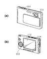
도 10a 및 10b는 본 발명이 적용되는 디지털 카메라의 외관을 나타내는 사시도이며, 도 10a는 앞쪽에서 본 사시도, 도 10b는 뒤쪽에서 본 사시도다.
도 11은 본 발명이 적용되는 노트형 PC의 외관을 나타내는 사시도다.
도 12는 본 발명이 적용되는 비디오 카메라의 외관을 나타내는 사시도다.
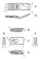
도 13a 내지 13g는 본 발명이 적용되는 휴대전화기를 나타내는 외관도이며, 13a는 연 상태에서의 정면도, 13b는 그 측면도, 13c는 닫은 상태에서의 정면도, 13d는 좌측면도, 13e는 우측면도, 13f는 평면도, 13g는 하면도다.1 is a system configuration showing an outline of the configuration of an organic EL display device according to an application example of the present invention.
2 is a circuit diagram showing a specific configuration example of a pixel (pixel circuit).
3 is a cross-sectional view showing an example of a cross-sectional structure of a pixel.
Fig. 4 is a timing waveform chart for explaining the basic circuit operation of the organic EL display device according to the application example of the present invention. Fig.
Fig. 5 is a circuit diagram showing the arrangement of constituent elements of a pixel in a general layout.
6 is a planar pattern diagrammatically showing constituent elements of a pixel in a general arrangement.
Fig. 7 is a circuit diagram showing the arrangement of the constituent elements of a pixel when taking a layout configuration according to an embodiment of the present invention. Fig.
Fig. 8 is a planar pattern diagrammatically showing a constituent element of a pixel when a layout configuration according to an embodiment of the present invention is taken. Fig.
Fig. 9 is a perspective view showing the appearance of a television set to which the present invention is applied. Fig.
10A and 10B are perspective views showing the appearance of a digital camera to which the present invention is applied, FIG. 10A is a perspective view seen from the front side, and FIG. 10B is a perspective view from behind.
11 is a perspective view showing the appearance of a notebook PC to which the present invention is applied.
12 is a perspective view showing the appearance of a video camera to which the present invention is applied.
Figs. 13A to 13G are external views showing a mobile phone to which the present invention is applied, 13a is a front view in a soft state, 13b is a side view thereof, 13c is a front view in a closed state, 13d is a left side view, , 13f is a plan view, and 13g is a bottom surface.
이하, 본 발명의 바람직한 실시예에 대해서 도면을 참조해서 상세하게 설명한다.Hereinafter, preferred embodiments of the present invention will be described in detail with reference to the drawings.
[시스템 구성][System configuration]
도 1은 본 발명이 적용되는 액티브 매트릭스형 표시장치의 구성의 개략을 나타내는 시스템 구성도다. 여기에서는, 액티브 매트릭스형 유기EL표시장치의 경우를 예로 들어서 설명한다. 유기EL표시장치는 디바이스에 흐르는 전류값에 따라 발광 휘도가 변화되는 전류 구동형 전기광학소자인 유기EL소자(유기전계 발광소자)를 각 화소(화소회로)의 발광소자로 사용한다.1 is a system configuration showing an outline of the configuration of an active matrix type display device to which the present invention is applied. Here, the case of an active matrix type organic EL display device will be described as an example. The organic EL display device uses an organic EL element (organic electroluminescent element), which is a current driven electro-optical element whose light emission luminance changes in accordance with the value of a current flowing in the device, as a light emitting element of each pixel (pixel circuit).
도 1에 나타낸 바와 같이, 본 적용예에 관련되는 유기EL표시장치(10)는, 화소 어레이부(30)와, 구동부를 포함한다. 화소 어레이부(30)는 화소(20)가 행렬형으로 2차원 배치되어서 이루어진다. 구동부는 그 화소 어레이부(30)의 주변에 배치되고, 각 화소(20)를 구동한다. 화소(20)를 구동하는 구동부로서는, 기록 주사 회로(40), 발광 구동주사 회로(50), 제1, 제2 보정용 주사 회로(60, 70) 및 수평구동회로(80)가 설치된다.As shown in Fig. 1, the organic
화소 어레이부(30)는, 통상, 유리 기판 등의 투명절연 기판 위에 형성되어, 플랫형의 패널구조로 되어 있다. 화소 어레이부(30)에는, m행n열의 화소배열에 대하여, 화소행마다 기록 주사선(31-1∼31-m)과 발광 제어 주사선(32-1∼32-m)과 제1 보정용 주사선(33-1∼33-m)과 제2 보정용 주사선(34-1∼34-m)이 각각 한 개씩 배선되어 있다. 또 화소열마다 신호선(데이터선)(35-1∼35-n) 중 한 개가 배선되어 있다.The
화소 어레이부(30)의 각 화소(20)는, 아모포스 실리콘TFT(Thin Film Transistor;박막 트랜지스터) 또는 저온 폴리실리콘TFT를 사용해서 형성할 수 있다. 저온 폴리실리콘TFT를 사용하는 경우에는, 기록 주사 회로(40), 발광 구동주사 회로(50), 제1, 제2 보정용 주사 회로(60, 70) 및 수평구동회로(80)도, 화소 어레이부(30)를 형성하는 표시 패널(기판) 위에 설치할 수 있다.Each
기록 주사 회로(40)는, 시프트 레지스터나 다른 구성 소자를 포함한다. 화소 어레이부(30)의 각 화소(20)에의 영상신호의 기록시에, 기록 주사 회로(40)는, 기록 주사선(31-1∼31-m)에 대하여 순차 기록 신호 WS1∼WSm을 공급함으로써 화소 어레이부(30)의 각 화소(20)를 행 단위로 순서대로 주사(선 순차 주사)한다.The
발광 구동주사 회로(50)는, 시프트 레지스터나 다른 구성 소자를 포함한다. 화소(20)의 발광 구동시에, 발광 구동주사 회로(50)는, 발광 제어 주사선(32-1∼32-m)에 대하여 순차 발광 제어신호 DS1∼DSm을 공급한다.The light emission
제1, 제2 보정용 주사 회로(60, 70)는, 시프트 레지스터나 다른 구성 소자를 포함한다. 제1 보정용 주사 회로(60)는, 후술하는 보정동작의 실행시에, 제1 보정용 주사선(33-1∼33-m)에 대하여 제1 주사 신호 AZ11∼AZ1m을 적절히 공급한다. 제2 보정용 주사 회로(70)는, 제2 보정용 주사선(34-1∼34-m)에 대하여 제2 보정용 주사 신호 AZ21∼AZ2m을 적절히 공급한다.The first and second
수평구동회로(80)는, 휘도정보에 따른 영상신호의 신호 전압 Vsig(이하, 간단히 「신호 전압 Vsig」이라고 할 경우도 있다)를, 기록 주사 회로(40)에 의한 주사에 동기해서 신호선(35-1∼35-n)에 공급한다. 이 수평구동회로(60)는, 예를 들면 신호 전압 Vsig를 행(라인) 단위로 기록하는 선 순차 기록의 구동형태를 취하고 있다.The
(화소회로)(Pixel circuit)
도 2는, 화소(화소회로)(20)의 구체적인 구성예를 게시하는 회로도다.2 is a circuit diagram showing a specific configuration example of the pixel (pixel circuit) 20. As shown in Fig.
도 2에 나타낸 바와 같이, 화소(20)는, 디바이스에 흐르는 전류값에 따라 발광 휘도가 변화되는 전류 구동형 전기광학소자, 예를 들면 유기EL소자(21)를 발광소자로서 포함한다. 그 유기EL소자(21)와 함께, 화소(20)는, 구동 트랜지스터(22), 기록(샘플링) 트랜지스터(23), 스위칭 트랜지스터(24∼26), 저장용량(27) 및 보조용량(28)을 구성 소자로서 포함한다.As shown in Fig. 2, the
상기 구성의 화소(20)에 있어서는, 구동 트랜지스터(22), 기록 트랜지스터(23) 및 스위칭 트랜지스터(25, 26)로서 N채널형 TFT를 사용한다. 스위칭 트랜지스터(24)로서 P채널형 TFT를 사용한다. 다만, 여기에서의 구동 트랜지스터(22), 기록 트랜지스터(23) 및 스위칭 트랜지스터(24∼26)의 도전형의 조합은 일례에 지나지 않고, 이것들의 조합에 한정되는 것이 아니다.In the
유기EL소자(21)는, 캐소드 전극이 제1 전원전위 Vcat(여기에서는, 접지전위 GND)에 접속되어 있다. 구동 트랜지스터(22)는, 유기EL소자(21)를 전류 구동하기 위한 능동소자이다. 구동 트랜지스터(22)는, 소스 전극이 유기EL소자(21)의 애노드 전극에 접속되어서 소스 폴로워 회로를 형성하고 있다.In the
기록 트랜지스터(23)는, 드레인 전극이 신호선(35)(35-1∼35-n 중 하나)에 접속되어 있고, 소스 전극이 구동 트랜지스터(22)의 게이트 전극에 접속되어 있고, 게이트 전극이 기록 주사선(31)(31-1∼31-m 중 하나)에 접속되어 있다.In the
스위칭 트랜지스터(24)는, 소스 전극이 제2 전원전위 Vccp(여기에서는, 양의 전원전위)에 접속되어 있고, 드레인 전극이 구동 트랜지스터(22)의 드레인 전극에 접속되어 있고, 게이트 전극이 발광 제어 주사선(32)(32-1∼32-m 중 하나)에 접속되어 있다.In the switching
스위칭 트랜지스터(25)는, 드레인 전극이 기록 트랜지스터(23)의 다른 쪽의 전극(구동 트랜지스터(22)의 게이트 전극)에 접속되어 있고, 소스 전극이 제3 전원전위 Vofs에 접속되어 있고, 게이트 전극이 제1 보정용 주사선(33)(33-1∼33-m 중 하나)에 접속되어 있다.The switching
스위칭 트랜지스터(26)는, 드레인 전극이 구동 트랜지스터(22)의 소스 전극과 유기EL소자(21)의 애노드 전극과의 접속 노드 N11에 접속되어 있고, 소스 전극이 제4 전원전위 Vini(여기에서는, 음의 전원전위)에 접속되어 있고, 게이트 전극이 제2 보정용 주사선(34)(34-1∼34-m 중 하나)에 접속되어 있다.The switching
저장용량(27)은, 한쪽의 전극이 구동 트랜지스터(22)의 게이트 전극과 기록 트랜지스터(23)의 드레인 전극과의 접속 노드 N12에 접속되어 있다. 저장용량(27)은, 다른 쪽의 전극이 구동 트랜지스터(22)의 소스 전극과 유기EL소자(21)의 애노드 전극과의 접속 노드 N11에 접속되어 있다.One electrode of the
보조용량(28)은, 한쪽의 전극이 구동 트랜지스터(22)의 소스 전극과 유기EL소자(21)의 애노드 전극과의 접속 노드 N11에 접속되어 있다. 보조용량(28)은, 다른 쪽의 전극이 고정 전위, 예를 들면 전원전위 Vccp에 접속되어 있다. 이 보조용량(28)은, 유기EL소자(21)의 용량부족을 보충하기 위해서 설치된 보조적인 것이다. 따라서 보조용량(28)은 화소(20)의 구성 소자로서 필수적인 것이 아니다.One electrode of the
전술한 접속 관계에서 각 구성 소자가 접속되어서 이루어진 화소(20)에 있어서, 각 구성 소자는 다음과 같은 작용을 한다.In the
즉, 기록 트랜지스터(23)는, 기록 주사 회로(40)로부터 기록 주사선(31)을 통해서 주어지는 기록 신호 WS에 응답해서 도통 상태가 된다. 기록 트랜지스터(23)는, 신호선(35)을 통해 공급되는 신호 전압 Vsig를 샘플링해서 화소(20) 내에 기록한다. 기록 트랜지스터(23)에 의해 기록된 신호 전압 Vsig는, 구동 트랜지스터(22)의 게이트 전극에 인가되는 동시에 저장용량(27)에 유지된다.In other words, the
구동 트랜지스터(22)는, 스위칭 트랜지스터(24)가 도통 상태에 있을 때에, 제2 전원전위 Vccp로부터 전류의 공급을 받는다. 이에 따라 저장용량(27)에 유지된 신호 전압 Vsig의 전압값에 따른 전류값의 구동전류를 유기EL소자(21)에 공급함으로써 그 유기EL소자(21)를 구동한다(전류 구동).The driving
구동 트랜지스터(22)는, 포화 영역에서 동작하도록 설계되어 있다. 따라서 구동 트랜지스터는 정전류원으로서 동작한다. 그 결과, 유기EL소자(21)에는, 구동 트랜지스터(22)로부터 다음 식 (1)로 주어지는 일정한 드레인-소스간 전류 Ids가 공급된다.The driving
Ids=(1/2)·μ(W/L)Cox(Vgs-Vth)2……(1)Ids = (1/2) 占 (W / L) Cox (Vgs-Vth)2 ... ... (One)
여기에서, Vth는 구동 트랜지스터(22)의 임계값전압, μ는 구동 트랜지스터(22)의 채널을 구성하는 반도체 박막의 이동도(이하, 간단히 「구동 트랜지스터(22)의 이동도」라고 한다), W는 채널 폭, L은 채널 길이, Cox는 단위면적당 게이트 용량, Vgs는 소스 전위를 기준으로 게이트에 인가되는 게이트-소스간 전압이다.Here, Vth is the threshold voltage of the driving
스위칭 트랜지스터(24)는, 발광 구동주사 회로(50)에 의해 발광 제어 주사선(32)을 통해서 주어지는 발광 구동신호 DS에 응답해서 도통 상태가 된다. 동시에 스위칭 트랜지스터(24)는, 전원전위 Vcc p으로부터 구동 트랜지스터(22)에 전류를 공급한다. 즉, 스위칭 트랜지스터(24)는, 구동 트랜지스터(22)에의 전류의 공급/정지의 제어를 행하는 것에 의해, 유기EL 소자(21)의 발광/비발광을 제어해서 듀티(Duty) 구동을 행하는 발광 제어 트랜지스터다.The switching
스위칭 트랜지스터(25)는, 제1 보정용 주사 회로(60)로부터 제1 보정용 주사선(33)을 통해서 주어지는 제1 보정용 주사 신호 AZ1에 응답해서 도통 상태가 된다. 동시에 스위칭 트랜지스터(25)는, 기록 트랜지스터(23)에 의한 영상신호의 신호 전압 Vsig의 기록에 앞서, 구동 트랜지스터(22)의 게이트 전위 Vg를 제3 전원전위 Vofs로 초기화한다. 여기에서, 제3 전원전위 Vofs는, 영상신호의 기준이 되는 전위(기준전위)로 설정되어 있다.The switching
스위칭 트랜지스터(26)는, 제2 보정용 주사 회로(70)로부터 제2 보정용 주사선(34)을 통해서 주어지는 제2 보정용 주사 신호 AZ2에 응답해서 도통 상태가 된다. 동시에 스위칭 트랜지스터(26)는, 기록 트랜지스터(23)에 의한 영상신호의 신호 전압 Vsig의 기록에 앞서, 구동 트랜지스터(22)의 소스 전위 Vs를 제4 전원전위 Vini로 초기화한다.The switching
화소(20)의 정상적인 동작을 보증하기 위한 조건으로서, 제4 전원전위 Vini은, 제3 전원전위 Vofs에서 구동 트랜지스터(22)의 임계값전압 Vth를 감산한 전위보다도 낮아지도록 설정되어 있다. 즉, Vini<Vofs-Vth의 레벨 관계를 만족한다.The fourth power supply potential Vini is set to be lower than the potential obtained by subtracting the threshold voltage Vth of the driving
또한 유기EL소자(21)의 캐소드 전위 Vcat(여기에서는, 접지전위 GND)에 유기 EL소자(21)의 임계값전압 Vthel을 가산한 레벨은, 제3 전원전위 Vofs에서 구동 트랜지스터(22)의 임계값전압 Vth를 감산한 레벨보다도 높아지도록 설정되어 있다. 즉, Vcat+Vthel>Vofs-Vth(>Vini)의 레벨 관계를 만족한다.The level obtained by adding the threshold voltage Vthel of the
저장용량(27)은, 기록 트랜지스터(23)에 의해 기록된 영상신호의 신호 전압 Vsig를 유지하는 동시에, 표시 기간에 걸쳐서 구동 트랜지스터(22)의 게이트-소스간의 전위차를 유지한다.The
(화소구조)(Pixel structure)
도 3은, 화소(20)의 단면구조의 일례를 게시하는 단면도다. 도 3에 나타낸 바와 같이, 화소(20)는 유리 기판(201) 위에 순차적으로 형성된 절연막(202), 절연 평탄화 막(203) 및 윈도우 절연막(204)을 포함한다. 유리 기판(201)은 그 위에 형성된 구동 트랜지스터(22), 기록 트랜지스터(23) 및 다른 구성 소자를 각각 포함하는 화소회로를 가진다. 화소(20)는 윈도우 절연막(204)의 오목부(204A)에 설치된 유기EL소자(21)도 포함한다.3 is a sectional view showing an example of the cross-sectional structure of the
유기EL소자(21)는, 상기 윈도우 절연막(204)의 오목부(204A)의 저부에 형성된 금속 등으로 된 애노드 전극(205)를 포함한다. 유기EL소자(21)는, 그 애노드 전극(205) 위에 형성된 유기층(전자수송층, 발광층, 홀 수송층/홀 주입층)(206)을 더 포함한다. 유기EL소자(21)는 그 유기층(206) 위에 전 화소에 공통으로 형성된 캐소드 전극(207)을 더 포함한다. 유기EL소자(21)는 예를 들면 투명도전막으로 이루어진다.The
유기EL소자(21)에 있어서, 유기층(206)은, 애노드 전극(205) 위에 홀 수송층/홀 주입층(2061), 발광층(2062), 전자수송층(2063) 및 전자주입층(도시 생략)이 순차 퇴적됨으로써 형성된다. 그리고 도 2의 구동 트랜지스터(22)로부터 애노드 전극(205)을 통해서 유기층(206)에 전류가 흐른다. 이에 따라 그 유기층(206) 내의 발광층(2062)에서 전자와 정공이 재결합하여 발광하게 되어 있다.A hole injection layer /
도 3에 나타낸 바와 같이, 화소회로가 형성된 유리 기판(201) 위에, 유기EL소자(21)가 형성된다. 유기EL소자(21)는 절연막(202), 절연 평탄화 막(203) 및 윈도우 절연막(204)을 통해 화소 단위로 형성된다. 형성 후에는, 패시베이션 막(208)을 통해 밀봉기판(209)이 접착제(210)에 의해 접합되어, 그 밀봉기판(209)에 유기EL소자(21)가 밀봉됨으로써, 표시 패널이 형성된다.As shown in Fig. 3,
(회로 동작의 설명)(Explanation of circuit operation)
계속해서, 상기 구성의 화소(20)를 행렬 모양으로 2차원 배치해서 이루어진 본 적용예에 관련되는 액티브 매트릭스형 유기EL표시장치(10)의 기본적인 회로 동작에 대해서, 도 4의 타이밍 파형도를 사용하여 설명한다.4 is used for the basic circuit operation of the active matrix organic
도 4에는, 어떤 화소행의 각 화소(20)를 구동할 때에, 기록 주사 회로(40)로부터 화소(20)에 주어지는 기록 신호 WS(WS1∼WSm 중 하나), 발광 구동주사 회로(50)로부터 화소(20)에 주어지는 발광 구동신호 DS(DS1∼DSm 중 하나) 및 제1, 제2 보정용 주사 회로(60, 70)로부터 화소(20)에 주어지는 제1, 제2 보정용 주사 신호 AZ1(AZ11∼AZ1 m 중 하나), AZ2(AZ21∼AZ2m 중 하나)의 타이밍 관계를 나타낸다. 도 4는 또한 구동 트랜지스터(22)의 게이트 전위 Vg 및 소스 전위 Vs의 변화를 나타낸다.4 shows an example in which each
여기에서, 기록 트랜지스터(23) 및 스위칭 트랜지스터(25, 26)는 N채널형 트랜지스터다. 따라서 기록 주사 신호 WS 및 제1, 제2 보정용 주사 신호 AZ1, AZ2에 있어서는, 고레벨(본 예에서는, 전원전위 Vccp;이하, 「“H”레벨」이라고 한다)의 상태가 액티브 상태가 되고, 저레벨(본 예에서는, 전원전위 Vcat(GND);이하, 「“L”레벨」이라고 한다)의 상태가 비액티브 상태가 된다. 또한 스위칭 트랜지스터(24)는 P채널형이다. 따라서 발광 구동신호 DS에 있어서는, “L”레벨의 상태가 액티브 상태가 되고, “H”레벨의 상태가 비액티브 상태가 된다.Here, the
시간 t1에 발광 구동신호 DS가 “L”레벨에서 “H”레벨로 전환되면, 스위칭 트랜지스터(24)가 비도통 상태(OFF 상태)가 된다. 이 상태에서, 시간 t2에 제2 보정용 주사 신호 AZ2가 “L”레벨에서 “H”레벨로 전환되면, 스위칭 트랜지스터(26)가 도통 상태(ON 상태)가 된다.When the light emission drive signal DS is switched from the "L" level to the "H" level at the time t1, the switching
스위칭 트랜지스터(26)가 도통 상태가 됨으로써, 구동 트랜지스터(22)의 소스 전극에는, 스위칭 트랜지스터(26)를 통해 제4 전원전위 Vini가 인가된다. 즉, 영상신호의 신호 전압 Vsig의 기록에 앞서, 구동 트랜지스터(22)의 소스 전위 Vs는, 전원전위 Vini로 초기화된다.As the switching
이 때, 전술한 바와 같이, Vini<Vcat+Vthel의 레벨 관계를 만족하다. 따라서 유기EL소자(21)는 역 바이어스 상태가 된다. 따라서, 유기EL소자(21)에는 전류가 흐르지 않아, 비발광 상태에 있다.At this time, as described above, the level relationship of Vini <Vcat + Vthel is satisfied. Therefore, the
다음에 시간 t3에 제1 보정용 주사 신호 AZ1이 “L”레벨에서 “H”레벨로 전환되면, 스위칭 트랜지스터(25)가 도통 상태가 된다. 이에 따라 구동 트랜지스터(22)의 게이트 전극에는, 스위칭 트랜지스터(25)를 통해 제3 전원전위 Vofs가 인가된다. 즉, 영상신호의 신호 전압 Vsig의 기록에 앞서, 구동 트랜지스터(22)의 게이트 전위 Vg는, 전원전위 Vofs로 초기화된다.Next, when the first correction scanning signal AZ1 is switched from the "L" level to the "H" level at the time t3, the switching
이 때, 구동 트랜지스터(22)의 게이트-소스간 전압 Vgs는, Vofs-Vini의 값을 취한다. 여기에서, 전술한 바와 같이, Vofs-Vini>Vth의 레벨 관계를 만족한다.At this time, the gate-source voltage Vgs of the driving
<임계값 보정기간><Threshold value correction period>
다음에 시간 t4에 제2 보정용 주사 신호 AZ2가 “H”레벨에서 “L”레벨로 전환되면, 스위칭 트랜지스터(26)가 비도통 상태가 된다. 그 후에 시간 t5에 발광 구동신호 DS가 “H”레벨에서 “L”레벨로 전환되면, 스위칭 트랜지스터(24)가 도통 상태가 된다. 이에 따라 전원전위 Vccp로부터 스위칭 트랜지스터(24)을 통해서 구동 트랜지스터(22)에는, 그 게이트-소스간 전압 Vgs에 따른 값의 전류가 흐른다.Next, when the second correction scanning signal AZ2 is switched from the "H" level to the "L" level at time t4, the switching
이 때, 구동 트랜지스터(22)의 소스 전위 Vs보다도 유기EL소자(21)의 캐소드 전위 Vcat가 높다. 따라서 유기EL소자(21)가 역 바이어스 상태에 있다. 따라서, 구동 트랜지스터(22)로부터 흐르는 전류가 노드 N11→저장용량(27)→노드 N12→스위칭 트랜지스터(25)→전원전위 Vofs의 경로로 흐른다. 따라서, 그 전류에 따른 전하가 저장용량(27)에 충전된다.At this time, the cathode potential Vcat of the
한편 저장용량(27)의 충전에 따라 구동 트랜지스터(22)의 소스 전위 Vs가 전원전위 Vini로부터 시간의 경과와 함께 서서히 상승한다. 그리고, 일정 시간이 경과한 후, 구동 트랜지스터(22)의 게이트-소스간 전압 Vgs가 그 구동 트랜지스터(22)의 임계값전압 Vth와 동일해지면, 구동 트랜지스터(22)가 컷오프한다.On the other hand, as the
구동 트랜지스터(22)가 컷오프함으로써 그 구동 트랜지스터(22)에 전류가 흐르지 않게 된다. 그 결과, 구동 트랜지스터(22)의 게이트-소스간 전압 Vgs, 즉 임계값전압 Vth가 임계값 보정용의 전압으로서 저장용량(27)에 유지된다.The current does not flow to the driving
그 후에 시간 t6에 발광 구동신호 DS가 “L”레벨에서 “H”레벨로 전환되면, 스위칭 트랜지스터(24)가 비도통 상태가 된다. 이 시간 t5에서 시간 t6까지의 기간이 구동 트랜지스터(22)의 임계값전압 Vth를 검출해서 저장용량(27)에 유지하는 기간이다.Thereafter, when the light emission drive signal DS is switched from the "L" level to the "H" level at time t6, the switching
여기에서는, 편의상, 시간 t5에서 시간 t6까지의 일정 기간(t5-t6)을 임계값 보정기간이라고 부르는 것으로 한다. 그 후에 시간 t7에 제1 보정용 주사 신호 AZ1이 “H”레벨에서 “L”레벨로 전환되면, 스위칭 트랜지스터(25)가 비도통 상태가 된다.For the sake of convenience, a constant period (t5-t6) from time t5 to time t6 is referred to as a threshold correction period. Thereafter, when the first correction scanning signal AZ1 is switched from the "H" level to the "L" level at time t7, the switching
<신호 기록기간><Signal writing period>
계속해서, 시간 t8에 기록 신호 WS가 “L”레벨에서 “H”레벨로 전환되면, 기록 트랜지스터(23)가 도통 상태가 되어, 기록 트랜지스터(23)가 영상신호의 신호 전압 Vsig를 샘플링하여, 화소 내에 기록하게 된다. 그 결과, 구동 트랜지스터(22)의 게이트 전위 Vg가 신호 전압 Vsig와 같아진다.Subsequently, when the write signal WS is switched from the "L" level to the "H" level at time t8, the
신호 전압 Vsig는 저장용량(27)에 유지된다. 이 때, 구동 트랜지스터(22)의 소스 전위 Vs는, 기록 트랜지스터(23)에 의한 샘플링시의 구동 트랜지터(22)의 게이트 전위 Vg의 진폭에 대하여, 저장용량(27)과 유기EL소자(21)와의 용량 커플링에 의해 상승한다.The signal voltage Vsig is held in the
여기에서, 유기EL소자(21)가 가지는 용량성분의 용량값을 Coled, 저장용량(27)의 용량값을 Cs, 보조용량(28)의 용량값을 Csub, 구동 트랜지스터(22)의 게이트 전위 Vg의 상승분을 ΔVg라고 하면, 구동 트랜지스터(22)의 소스 전위 Vs의 상승분 ΔVs는, 다음 식 (2)로 주어진다.Assuming that the capacitance value of the capacitance component of the
ΔVs=ΔVg×{Cs/(Coled+Cs+Csub)}……(2)? Vs =? Vg × {Cs / (Coled + Cs + Csub)} ... ... (2)
한편, 기록 트랜지스터(23)에 의한 샘플링에 의해 기록된 신호 전압 Vsig는, 저장용량(27)에 유지되어, 신호 전압 Vsig는 저장용량(27)에 의해 유지된 임계값전압 Vth에 가산된다.On the other hand, the signal voltage Vsig recorded by the sampling by the
이 때, 영상신호의 기록 게인(영상신호의 신호 전압 Vsig에 대한 저장용량(27)의 유지 전압의 비율)이 1(이상값)이라고 가정하면, 저장용량(27)의 유지 전압은 Vsig-Vofs+Vth가 된다. 여기에서, 이해를 쉽게 하기 위해서, Vofs=0V라고 하면, 게이트-소스간 전압 Vgs는, Vsig+Vth가 된다.Assuming that the recording gain of the video signal (the ratio of the holding voltage of the
이렇게, 저장용량(27)에 미리 임계값전압 Vth를 유지해 둠으로써 구동 트랜지스터(22)의 임계값전압 Vth의 화소 사이의 편차나 시간에 따른 변화를 보정할 수 있다. 즉, 신호 전압 Vsig에 의한 구동 트랜지스터(22)의 구동시에, 그 구동 트랜지스터(22)의 임계값전압 Vth가 저장용량(27)에 유지한 임계값전압 Vth와 상쇄된다. 즉, 임계값전압 Vth의 보정이 이루어진다.By holding the threshold voltage Vth in advance in the
임계값전압 Vth의 보정동작에 의해, 화소마다 임계값전압 Vth에 편차나 시간에 따른 변화가 있더라도, 구동 트랜지스터(22)에 의한 유기EL소자(21)의 구동에 대한 임계값전압 Vth의 영향을 캔슬 할 수 있다. 그 결과, 임계값전압 Vth의 화소 사이의 편차나 시간에 따른 변화의 영향을 받지 않고, 유기EL소자(21)의 발광 휘도를 일정하게 유지할 수 있다.The influence of the threshold voltage Vth for the drive of the
<이동도 보정기간><Mobility correction period>
그 후에 기록 트랜지스터(23)가 도통인 상태에서, 시간 t9에 발광 구동신호 DS가 “H”레벨에서 “L”레벨로 전환되면, 스위칭 트랜지스터(24)가 도통 상태가 된다. 이에 따라 전원전위 Vccp로부터 구동 트랜지스터(22)에의 전류공급이 개시된다. 여기에서, Vofs-Vth<Vthel로 설정해 두는 것에 의해, 유기EL소자(21)가 역 바이어스 상태에 놓인다.Thereafter, when the light emitting drive signal DS is switched from the "H" level to the "L" level at the time t9 in the state in which the
유기EL소자(21)가 역 바이어스 상태에 있을 때 그 유기EL소자(21)는 다이오드 특성이 아닌 단순한 용량 특성을 나타내게 된다. 따라서, 구동 트랜지스터(22)에 흐르는 드레인-소스간 전류 Ids는, 저장용량(27)의 용량값 Cs와, 보조용량(28)의 용량값 Csub와, 유기EL소자(21)의 용량성분의 용량값 Coled를 합성한 용량 C(=Cs+Csub+Coled)에 기록되어 간다. 이 기록에 의해, 구동 트랜지스터(22)의 소스 전위 Vs가 상승한다.When the
구동 트랜지스터(22)의 소스 전위 Vs의 상승분 ΔVs는, 저장용량(27)에 유지된 게이트-소스간 전압 Vgs로부터 감산되도록, 바꾸어 말하면, 저장용량(27)의 충전 전하를 방전하도록 작용한다. 이는 부귀환이 걸린다는 것을 의미한다. 즉, 구동 트랜지스터(22)의 소스 전위 Vs의 상승분 ΔVs는 부귀환의 귀환량이 된다. 이 때, 구동 트랜지스터(22)의 게이트-소스간 전압 Vgs는, Vsig-ΔVs+Vth가 된다.The increase DELTA Vs of the source potential Vs of the
이렇게, 구동 트랜지스터(22)에 흐르는 전류(드레인-소스간 전류 Ids)를 그 구동 트랜지스터(22)의 게이트 입력(게이트-소스간의 전위차)에 부귀환함으로써, 각 화소(20)에 있어서의 구동 트랜지스터(22)의 드레인-소스간 전류 Ids의 이동도 μ에 대한 의존성을 상쇄할 수 있다. 즉, 구동 트랜지스터(22)의 이동도 μ의 화소 사이의 편차를 보정할 수 있다.In this manner, the current (drain-source current Ids) flowing in the driving
도 4에 있어서, 기록 신호 WS의 액티브 기간(“H”레벨 기간)과 발광 구동신호 DS의 액티브 기간(“L”레벨 기간)이 오버랩하는 기간(t9-t10의 기간), 즉 기록 트랜지스터(23)와 스위칭 트랜지스터(24)가 모두 도통 상태가 되는 오버랩 기간 T가 이동도 보정기간이 된다.4, the period (t9-t10) in which the active period ("H" level period) of the write signal WS and the active period ("L" level period) And the switching
여기에서, 이동도 μ가 상대적으로 높은 구동 트랜지스터와 이동도 μ가 상대적으로 낮은 구동 트랜지스터를 생각해본다. 이동도 μ가 높은 구동 트랜지스터는, 이동도 μ가 낮은 구동 트랜지스터에 비해 소스 전위 Vs가 크게 상승한다. 또한 소스 전위 Vs가 크게 상승할수록, 구동 트랜지스터(22)의 게이트-소스간 전압 Vgs는 작아진다. 그 결과 전류가 흐르기 어려워진다.Here, a drive transistor having a relatively high mobility μ and a drive transistor having a relatively low mobility μ are considered. The driving transistor having a high mobility μ has a higher source potential Vs than a driving transistor having a low mobility μ. In addition, the gate-source voltage Vgs of the driving
요컨대, 이동도 보정기간 T를 조정함으로써 이동도 μ가 다른 구동 트랜지스터(22)를 통해 같은 드레인·소스간 전류 Ids를 흘려보낼 수 있다. 이 이동도 보정기간 T에 의해 결정한 구동 트랜지스터(22)의 게이트-소스간 전압 Vgs를 저장용량(27)에 유지하고, 그 게이트-소스간 전압 Vgs에 따른 전류(드레인-소스간 전류 Ids)를 구동 트랜지스터(22)로부터 유기EL소자(21)에 흐르게 함으로써 그 유기EL소자(21)가 발광한다.In short, by adjusting the mobility correction period T, the same drain-source current Ids can be passed through the driving
<발광 기간>≪ Light emission period &
시간 t10에 기록 신호 WS가 “L”레벨이 되어, 기록 트랜지스터(23)가 비도통 상태가 된다. 그 결과 이동도 보정기간 T가 종료하고, 발광 기간에 들어간다. 이 발광 기간에는, 구동 트랜지스터(22)의 소스 전위 Vs가 유기EL소자(21)의 구동전압까지 상승한다.At time t10, the write signal WS becomes the "L" level, and the
한편 기록 트랜지스터(23)가 비도통 상태가 됨으로써 구동 트랜지스터(22)의 게이트 전극이 신호선(35)(35-1∼35-n 중 하나)으로부터 분리되어 플로팅 상태에 있다. 따라서 저장용량(27)에 의한 부트스트랩 동작에 의해, 게이트 전위 Vg가 소스 전위 Vs에 연동해서 상승한다.On the other hand, the gate electrode of the driving
그리고 구동 트랜지스터(22)의 소스 전위 Vs의 상승에 따라, 유기EL소자(21)는 역 바이어스 상태가 해소되어, 순 바이어스 상태가 된다. 이에 따라 구동 트랜지스터(22)로부터 유기EL소자(21)에 대하여 전술한 식 (1)로 주어지는 일정한 드레인-소스간 전류 Ids가 공급되어, 유기EL소자(21)는 실제로 발광을 시작한다.As the source potential Vs of the driving
이 때의 드레인-소스간 전류 Ids 대 게이트-소스간 전압 Vgs의 관계는, 전술한 식 (1)의 Vgs에 Vsig-ΔVs+Vth를 대입함으로써 다음 식 (3)으로 주어진다.The relationship between the drain-source current Ids and the gate-source voltage Vgs at this time is given by the following equation (3) by substituting Vsig -? Vs + Vth for Vgs in the above equation (1).
Ids=kμ(Vgs-Vth)2Ids = kμ (Vgs-Vth)2
=kμ(Vsig-ΔVs)2……(3)= kμ (Vsig-ΔVs)2 ... ... (3)
여기에서, k=(1/2)(W /L)Cox다.Here, k = (1/2) (W / L) Cox.
식 (3)으로부터 분명하게 나타낸 바와 같이, 구동 트랜지스터(22)의 임계값전압 Vth의 항이 캔슬된다. 구동 트랜지스터(22)로부터 유기EL소자(21)에 공급되는 드레인-소스간 전류 Ids는, 구동 트랜지스터(22)의 임계값전압 Vth에 의존하지 않는다.The term of the threshold voltage Vth of the driving
기본적으로, 구동 트랜지스터(22)의 드레인-소스간 전류 Ids는, 영상신호의 신호 전압 Vsig에 의해 정해진다. 환언하면, 유기EL소자(21)는, 구동 트랜지스터(22)의 임계값전압 Vth의 화소 사이의 편차나 시간에 따른 변화의 영향을 받지 않고, 영상신호의 신호 전압 Vsig에 따른 휘도로 발광한다.Basically, the drain-source current Ids of the driving
이렇게, 영상신호의 신호 전압 Vsig가 기록되기 전에 구동 트랜지스터(22)의 임계값전압 Vth를 미리 저장용량(27)에 유지해 둔다. 이로써 구동 트랜지스터(22)의 임계값전압 Vth를 캔슬(보정)하여, 그 임계값전압 Vth의 화소 사이의 편차나 시간에 따른 변화의 영향을 받지 않는 일정한 드레인-소스간 전류 Ids를 유기EL소자(21)에 흐르게 할 수 있다. 이에 따라 고화질의 표시 화상을 얻을 수 있다(구동 트랜지스터(22)의 Vth 변동에 대한 보상 기능).Thus, the threshold voltage Vth of the driving
또한 상기의 식 (3)으로부터 분명하게 나타낸 바와 같이, 영상신호의 신호 전압 Vsig는, 드레인-소스간 전류 Ids의 구동 트랜지스터(22)의 게이트 입력에의 부귀환에 의해 귀환량 ΔVs로 보정되어 있다. 이 귀환량 ΔVs는 식 (3)의 계수부에 위치하는 이동도 μ의 효과를 상쇄되도록 작용한다.Further, as clearly shown in the above equation (3), the signal voltage Vsig of the video signal is corrected by the feedback amount? Vs by the negative feedback of the drain-source current Ids to the gate input of the driving
따라서, 드레인-소스간 전류 Ids는, 실질적으로 영상신호의 신호 전압 Vsig에만 의존하게 된다. 즉, 유기EL소자(21)는, 구동 트랜지스터(22)의 임계값전압 Vth뿐만 아니라, 구동 트랜지스터(22)의 이동도 μ의 화소 사이의 편차나 시간에 따른 변화의 영향을 받지 않고, 신호 전압 Vsig에 따른 휘도로 발광한다. 그 결과, 라인이나 휘도 불균일이 없는 균일한 화질을 얻을 수 있다.Therefore, the drain-source current Ids is substantially dependent only on the signal voltage Vsig of the video signal. That is, the
이렇게, 이동도 보정기간 T(t9-t10)에, 드레인-소스간 전류 Ids를 구동 트랜지스터(22)의 게이트 입력에 부귀환하고, 그 귀환량 ΔVs로 신호 전압 Vsig를 보정한다. 이로써 구동 트랜지스터(22)의 드레인-소스간 전류 Ids의 이동도 μ에 대한 의존성을 상쇄하여, 신호 전압 Vsig에만 의존하는 드레인-소스간 전류 Ids를 유기EL소자(21)에 흐르게 할 수 있다. 이에 따라 구동 트랜지스터(22)의 이동도 μ의 화소 사이의 편차나 시간에 따른 변화에 기인하는 라인이나 휘도 불균일이 없는 균일한 화질의 표시 화상을 얻을 수 있다(구동 트랜지스터(22)의 이동도 μ에 대한 보상 기능).Thus, in the mobility correction period T (t9-t10), the drain-source current Ids is made negative at the gate input of the driving
여기에서, 전류 구동형 전기광학소자인 유기EL소자(21)를 포함한 화소(20)가 행렬 모양으로 배치되어 이루어진 유기EL표시장치(10)에 있어서는, 유기EL소자(21)의 발광 시간이 길어지면, 그 유기EL소자(21)의 I-V 특성이 변화되어버린다. 그 때문에, 유기EL소자(21)의 애노드 전극과 구동 트랜지스터(22)의 소스 전극과의 접속 노드 N11의 전위(구동 트랜지스터(22)의 소스 전위 Vs)도 변화된다.Here, in the organic
이에 반해 상기 구성의 액티브 매트릭스형 유기EL표시장치(10)에서는, 구동 트랜지스터(22)의 게이트-소스간에 접속된 저장용량(27)에 의한 부트스트랩 동작에 의해 구동 트랜지스터(22)의 게이트-소스간 전압 Vgs가 일정 값으로 유지된다. 이에 따라 유기EL소자(21)에 흐르는 전류는 변화되지 않는다. 따라서, 유기EL소자(21)의 I-V 특성이 열화하더라도, 일정한 드레인-소스간 전류 Ids가 유기EL소자(21)에 계속해서 흐른다. 이에 따라 유기EL소자(21)의 발광 휘도의 변화를 억제할 수 있다(유기EL소자(21)의 특성 변동에 대한 보상 기능).On the other hand, in the active matrix organic
[화소의 배치][Arrangement of pixels]
여기에서, 화소(20)를 구성하는 5개의 트랜지스터(22∼26), 저장용량(27) 및 보조용량(28)과, 기록 주사선(31), 발광 제어 주사선(32) 및 제1, 제2 보정용 주사선(33, 34)의 각 배선의 배치에 대해서 생각한다.Here, the five
(일반적인 화소의 배치)(Arrangement of typical pixels)
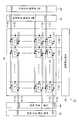
도 5는 화소(20)의 일반적인 배치시의 구성 소자의 배치를 나타내는 회로도다. 도 6에 그 평면 패턴을 모식적으로 나타낸다.Fig. 5 is a circuit diagram showing the arrangement of components in the general arrangement of the
화소(20)의 효율 좋은 배치를 고려하면, 일반적으로는, 도 5, 도 6에 나타낸 바와 같이, 제1, 제2 보정용 주사선(33, 34)을 화소(20)의 상하에 배선하고, 이들 주사선(33, 34)의 사이에 기록 주사선(31) 및 발광 제어 주사선(32)을 배선하고, 이들 주사선(31), 주사선(32)의 상하에 화소의 구성 소자를 배치하는 구성을 생각해 볼 수 있다.5 and 6, first and second
보다 구체적으로는, 제1 보정용 주사선(33)과 기록 주사선(31) 사이의 영역에 기록 트랜지스터(23)와 스위칭 트랜지스터(25)를 배치한다. 발광 제어 주사선(32)과 제2 보정용 주사선(34) 사이의 영역에 구동 트랜지스터(22)와 스위칭 트랜지스터(26)와 저장용량(27)과 보조용량(28)을 배치하는 배치 구성이 된다.More specifically, the
이러한 일반적인 배치 구성은, 배선 층간을 전기적으로 접속하는 콘택부의 수를 최소한으로 억제하여, 각 구성 소자를 효율적으로 배치하고자 하는 생각에 근거하는 것이다. 이 때 영상신호의 신호 전압 Vsig를 전송하는 신호선(35)과, 전원전위 Vccp, Vofs, Vini의 각 전원선(36, 37, 38)은, 화소열 방향(화소열의 화소의 배열 방향)을 따라 배선되어 있다.Such a general arrangement is based on the idea of minimizing the number of the contact portions electrically connecting the wiring layers to each other and arranging each component efficiently. At this time, the
도 6의 평면 패턴도에 있어서, 기록 주사선(31), 발광 제어 주사선(32), 제1, 제2 보정용 주사선(33, 34) 및 트랜지스터(22∼26)의 각 게이트 전극은, 유리 기판(201)(도 3 참조) 위에 몰리브덴(Mo) 등에 의해 1층째로서 배선된다. 트랜지스터(22∼26)의 각 반도체층은, 폴리실리콘(PS) 등에 의해 2층째로서 형성된다. 신호선(35) 및 전원선(36, 37, 38)은, 알루미늄(Al) 등에 의해 3층째로서 배선된다.6, each gate electrode of the
이들 배선층의 위치 관계는, 도 3에 나타내는 화소구조로부터 명확하다. 1층째와 2층째의 사이, 2층째와 3층째의 사이에는 각각 절연막이 개재되어 있다. 도 6으로부터 분명하게 나타낸 바와 같이, 상기한 일반적인 배치 구성을 취하는 것에 의해, 각 배선층을 전기적으로 접속하는 콘택부의 수를 12개 정도로 억제할 수 있다.The positional relationship of these wiring layers is clear from the pixel structure shown in Fig. An insulating film is interposed between the first layer and the second layer, and between the second layer and the third layer. As clearly shown in Fig. 6, by taking the general arrangement as described above, it is possible to reduce the number of contact portions for electrically connecting the respective wiring layers to about twelve.
그런데 상기한 일반적인 배치 구성에 있어서는, 구동 트랜지스터(22)의 게이트 전극과 기록 트랜지스터(23)의 소스 전극 및 스위칭 트랜지스터(25)의 드레인 전극을 전기적으로 접속하는 배선 패턴(306)이 기록 주사선(31) 및 발광 제어 주사선(32)의 각 배선 패턴과 교차한다(도 5, 도 6의 파선으로 둘러싸인 부분).The
[기생용량에 기인하는 문제점][Problems due to parasitic capacitance]
이와 같이, 구동 트랜지스터(22)의 게이트 전극에의 배선 패턴(306)이 기록 주사선(31) 및 발광 제어 주사선(32)의 각 배선 패턴과 교차하기 때문에, 그 교차 부분에 있어서 절연막(도 3의 절연막(202)에 상당)을 통해 기생용량이 형성된다. 이 기생용량은, 구동 트랜지스터(22)의 게이트 전극에 연결되는 기생용량(Cp)이 된다(도 2 참조).As described above, since the
전술한 부트스트랩 동작에 있어서, 이상적으로는, 구동 트랜지스터의 소스 전위 Vs의 상승분 ΔVs와 게이트 전위 Vg의 상승분 ΔVg는 동일해야 한다. 즉, 부트스트랩 게인 Gbst가 1이 되어야 한다. 그러나 구동 트랜지스터(22)의 게이트 전극에 결합된 기생용량에 의해 기생용량과 저장용량(27)의 사이에서 전하 분배가 발생하기 때문에, 부트스트랩 게인 Gbst가 감소한다.In the bootstrap operation described above, ideally, the increase? Vs of the source potential Vs of the drive transistor and the increase? Vg of the gate potential Vg must be the same. That is, the bootstrap gain Gbst must be 1. However, since the charge distribution occurs between the parasitic capacitance and the
여기에서, 구동 트랜지스터(22)의 게이트 전극에 결합된 기생용량의 용량값을 Cp라고 하면, 부트스트랩 게인 Gbst는Assuming that the capacitance value of the parasitic capacitance coupled to the gate electrode of the driving
Gbst=ΔVg/ΔVs=Cs/(Cs+Cp)……(4)Gbst =? Vg /? Vs = Cs / (Cs + Cp) ... (4)
로 표현된다. 식 (4)로부터 분명하게 나타낸 바와 같이, 구동 트랜지스터(22)의 게이트 전극에 결합된 기생용량의 용량값 Cp가 커질수록, 부트스트랩 게인 Gbst가 낮아진다.Lt; / RTI > As clearly shown in equation (4), the larger the capacitance value Cp of the parasitic capacitance coupled to the gate electrode of the driving
부트스트랩 게인 Gbst가 낮아지면, 게이트 전위 Vg의 상승분 ΔVg가 소스 전위 Vs의 상승분 ΔVs보다도 작아진다. 그 결과 부트스트랩 동작의 개시시보다도 구동 트랜지스터(22)의 게이트-소스간의 전위차가 작아진다. 이에 따라 유기EL소자(21)에 흐르게 하는 구동전류 Ids로서, 기록 트랜지스터(23)에 의해 기록한 영상신호의 신호 전압 Vsig에 대응한 전류를 확보할 수 없게 된다. 그 결과, 유기EL소자(21)의 발광 휘도가 낮아지고, 그에 따라 휘도 편차가 발생하여 화질의 열화를 초래한다.When the bootstrap gain Gbst is lowered, the increase? Vg of the gate potential Vg becomes smaller than the increase? Vs of the source potential Vs. As a result, the potential difference between the gate and the source of the driving
[본 실시예의 특징부분][Features of this embodiment]
이러한 이유로, 본 실시예에서는 화소(20)를 구성하는 5개의 트랜지스터(22∼26), 저장용량(27) 및 보조용량(28)과, 기록 주사선(31), 발광 제어 주사선(32) 및 제1, 제2 보정용 주사선(33, 34)의 각 배선의 배치, 특히 기록 주사선(31) 및 발광 제어 주사선(32)의 각 배선의 배치를 고안함으로써, 구동 트랜지스터(22)의 게이트 전극에 기생용량이 결합하지 않도록 하고 있다.For this reason, in the present embodiment, five
(본 실시예에 따른 화소의 배치)(Arrangement of pixels according to this embodiment)
도 7은, 본 발명의 일 실시예에 따른 배치 구성을 취할 때의 화소(20)의 구성 소자의 배치를 나타내는 회로도다. 도 8에 그 평면 패턴을 모식적으로 나타낸다. 도 7 및 도 8에 있어서, 도 5 및 도 6과 동등 부분에는 동일한 부호를 부착해서 나타낸다.7 is a circuit diagram showing the arrangement of the constituent elements of the
도 7, 도 8에 나타낸 바와 같이, 본 실시예에 따른 화소(20)의 배치에 있어서는, 제1, 제2 보정용 주사선(33, 34)을 화소(20)의 상하에 화소행 방향(화소행의 화소의 배열 방향)을 따라 배선한다. 이들 주사선(33, 34)의 외측에 기록 주사선(31) 및 발광 제어 주사선(32)을 화소행 방향을 따라 더 배선한다. 제1, 제2 보정용 주사선(33, 34) 사이의 영역에 구성 소자, 즉 5개의 트랜지스터(22∼26), 저장용량(27) 및 보조용량(28)을 배치한 구성을 취하고 있다.7 and 8, in the arrangement of the
전원전위 Vccp의 전원선(36)은, 화소(20)의 구성 소자의 좌외측에 화소열 방향을 따라 배선되어 있다. 또한 영상신호의 신호 전압 Vsig를 전송하는 신호선(35)과, 전원전위 Vofs, Vini의 각 전원선(37, 38)은, 화소(20)의 구성 소자의 우외측에 화소열 방향을 따라 배선되어 있다.The
도 8의 평면 패턴도에 있어서, 기록 주사선(31), 발광 제어 주사선(32), 제1, 제2 보정용 주사선(33, 34) 및 트랜지스터(22∼26)의 각 게이트 전극은, 유리 기판(201)(도 3 참조) 위에 몰리브덴(Mo) 등에 의해 1층째로서 배선된다. 트랜지스터(22∼26)의 각 반도체층은, 폴리실리콘(PS) 등에 의해 2층째로서 형성된다. 신호선(35) 및 전원선(36, 37, 38)은, 알루미늄(Al) 등에 의해 3층째로서 배선된다.8, the gate electrodes of the
여기에서, 기록 주사선(31)은 제1 보정용 주사선(33)의 외측, 즉 그 제1 보정용 주사선(33)을 사이에 두고 기록 트랜지스터(23)(일 예로서, 제2 트랜지스터)와 반대측에 배선되어 있다. 따라서 기록 트랜지스터(23)의 게이트 전극과 기록 주사선(31)의 사이에는 다음과 같은 배선구조가 사용된다.Here, the
즉, 기록 트랜지스터(23)의 게이트 전극(1층째의 Mo배선)은, 배선(일 예로서, 제2 배선)을 통하여, 화소열 방향을 따라 배선된 3층째의 배선 패턴(Al배선)(302)(일 예로서, 상호접속 배선)과 콘택부(301)에 의해 콘택이 이루어진다. 배선 패턴(302)과 1층째의 기록 주사선(31) 사이의 콘택은 콘택부(303)에 의해 이루어진다. 이에 따라 기록 주사선(31)과의 전기적인 접속이 확보된다.That is, the gate electrode (Mo wiring in the first layer) of the
또한 발광 제어 주사선(32)은 제2 보정용 주사선(34)의 외측, 즉 그 제2 보정용 주사선(34)을 사이에 두고 스위칭 트랜지스터(24)와 반대측 배선되어 있다. 따라서 스위칭 트랜지스터(24)의 게이트 전극과 발광 제어 주사선(32)의 사이에는 다음과 같은 배선구조가 사용된다.The emission
즉, 스위칭 트랜지스터(24)의 게이트 전극(1층째의 Mo배선)은, 화소열 방향을 따라 배선된 3층째의 배선 패턴(Al배선)(305)과 콘택부(304)에 의해 콘택이 이루어진다. 배선 패턴(305)과 1층째의 발광 제어 주사선(32) 사이의 콘택은 콘택부(304)에 의해 이루어진다. 이에 따라 발광 제어 주사선(32)과의 전기적인 접속이 확보된다.That is, the gate electrode (Mo wiring in the first layer) of the switching
(본 실시예의 작용 효과)(Function and effect of this embodiment)
이상의 설명 및 도 7, 도 8로부터 분명하게 나타낸 바와 같이, 본 실시예에 있어서, 구동 트랜지스터(22)(일 예로서 제1 트랜지스터), 그 구동 트랜지스터(22)의 게이트 전극에 접속된 기록 트랜지스터(23) 및 스위칭 트랜지스터(25)(일 예로서 제3 트랜지스터)를 적어도 가지는 화소 구성의 유기EL표시장치(10)에는 다음과 같은 이점이 있다. 즉, 기록 주사선(31), 바람직하게는 기록 주사선(31) 및 발광 제어 주사선(32)이, 구동 트랜지스터(22)의 게이트 전극에 연결되는 배선 패턴, 즉 구동 트랜지스터(22)의 게이트 전극과 기록 트랜지스터(23)의 소스 전극 및 스위칭 트랜지스터(25)의 드레인 전극을 전기적으로 접속하는 배선 패턴(306)(일 예로서 제1 배선)과 교차하지 않는 배선구조로 하고 있다.7 and 8, in this embodiment, the driving transistor 22 (the first transistor as an example), the writing transistor connected to the gate electrode of the driving
보다 구체적으로는, 화소(20)의 구성 소자가 배치되는 영역의 외측에 제1 보정용 주사선(33)을 배선한다. 그 제1 보정용 주사선(33)의 외측에 기록 주사선(31)을 더 배선한다. 이들 주사선(31, 33)의 배선층(본 예에서는, 1층째)과 다른 배선층(본 예에서는, 3층째)에 형성된 배선 패턴(302)을 통해 기록 주사선(31)을 기록 트랜지스터(23)의 게이트 전극과 전기적으로 접속한 구성을 채용한다. 이로써 기록 주사선(31)이 구동 트랜지스터(22)의 게이트 전극에 연결되는 배선 패턴(306)과 교차하지 않도록 하고 있다.More specifically, the first
또한 화소(20)의 구성 소자가 배치되는 영역을 사이에 두고 기록 주사선(31)과 반대측에 발광 제어 주사선(32)을 배선한다. 이 발광 제어 주사선(32)의 배선층(본 예에서는, 1층째)과 다른 배선층(본 예에서는, 3층째)에 형성된 배선 패턴(305)을 통해 발광 제어 주사선(32)을 스위칭 트랜지스터(발광 제어 트랜지스터)(24)의 게이트 전극과 전기적으로 접속한 구성을 채용한다. 이로써 발광 제어 주사선(32)가 구동 트랜지스터(22)의 게이트 전극에 연결되는 배선 패턴(306)과 교차하지 않도록 하고 있다.And the emission
상기한 바와 같이, 기록 주사선(31), 바람직하게는 기록 주사선(31) 및 발광 제어 주사선(32)이, 구동 트랜지스터(22)의 게이트 전극에 연결되는 배선 패턴(306)과 교차하지 않는 배선구조로 한다. 더 구체적으로는, 화소(20)의 구성 소자가 배치되는 영역의 한쪽에 기록 주사선(31)을, 다른 쪽에 발광 제어 주사선(32)을 각각 배선한다. 이로써, 구동 트랜지스터(22)의 게이트 전극에 기생용량이 결합하지 않도록 할 수 있다.The
여기에서는, 기록 주사선(31) 및 발광 제어 주사선(32) 모두, 구동 트랜지스터(22)의 게이트 전극에 연결되는 배선 패턴(306)과 교차하지 않는 배선구조로 했다. 그러나 적어도 기록 주사선(31)이 배선 패턴(306)과 교차하지 않는 배선구조로 한 경우여도, 전술한 바와 같이, 기록 주사선(31) 및 발광 제어 주사선(32)이 배선 패턴(306)과 교차할 경우에 비해, 구동 트랜지스터(22)의 게이트 전극에 결합하는 기생용량을 작게 할 수 있다.In this case, both the
이와 같이 하여, 구동 트랜지스터(22)의 게이트 전극에 기생용량이 결합하지 않도록 하거나 구동 트랜지스터(22)의 게이트 전극에 결합하는 기생용량을 최소화함으로써, 부트스트랩 동작시의 부트스트랩 게인 Gbst를 1, 또는 1에 가깝게 할 수 있다. 따라서 유기EL소자(21)에 흐르게 하는 구동전류 Ids로서, 기록 트랜지스터(23)에 의해 기록한 영상신호의 신호 전압 Vsig에 대응한 전류를 확보할 수 있다. 이에 따라 기생용량에 기인하는 발광 휘도의 저하를 억제할 수 있다. 그 결과 유기EL소자(21)의 발광 휘도의 저하를 억제할 수 있기 때문에, 화질의 향상을 꾀할 수 있다.In this manner, the parasitic capacitance coupled to the gate electrode of the driving
본 실시예의 경우에는, 전술한 일반적인 배치 구성을 취할 경우에 비해, 4개의 접속부가 더 필요하다. 이들 부가되는 접속부는 기록 주사선(31)과 기록 트랜지스터(23)의 게이트 전극을 전기적으로 접속하기 위한 2개의 콘택부(301, 303), 발광 제어 주사선(32)과 스위칭 트랜지스터(24)의 게이트 전극을 전기적으로 접속하기 위한 2개의 콘택부(304, 307)다. 그러나 콘택부가 약간 증가하는 결점보다도, 정상적인 부트스트랩 동작을 저해하는 요인이 되는 기생용량을 최소화함으로써 화질을 향상시키는 효과가 크다고 할 수 있다.In the case of this embodiment, as compared with the case of taking the general arrangement described above, further four connecting portions are required. These additional connecting portions include two
[변형예][Modifications]
상기 실시예에서는 구동 트랜지스터(22) 및 기록 트랜지스터(23), 스위칭 트랜지스터(24∼26)를 가지는 5Tr의 화소 구성의 유기EL표시장치에 적용했을 경우를 예로 들어 설명했다. 그러나 본 발명이 본 적용예에 한정되는 것은 아니고, 구동 트랜지스터(22), 그 구동 트랜지스터(22)의 게이트 전극에 접속된 기록 트랜지스터(23) 및 스위칭 트랜지스터(25)를 적어도 가지는 화소 구성의 유기EL 표시장치 전반에 대하여 적용 가능하다.The above embodiment has been described by taking as an example a case where the present invention is applied to an organic EL display device having a 5Tr pixel structure having the driving
또한 상기 실시예에서는 본 발명을 유기EL소자를 사용한 유기 EL표시장치에 적용했을 경우를 예로 들어서 설명했다. 그러나 본 발명이 본 적용예에 한정되는 것은 아니고, 전기광학소자를 포함한 화소가 행렬 모양으로 배치되어 이루어진 플랫 패널형의 표시장치 전반에 대하여 적용 가능하다.Further, in the above embodiments, the case where the present invention is applied to the organic EL display device using the organic EL element has been described as an example. However, the present invention is not limited to this application example, but can be applied to a general flat panel display device in which pixels including electro-optical elements are arranged in a matrix.
[적용예][Application example]
이상 설명한 본 발명에 의한 표시장치는, 일례로서, 도 9∼도 13에 나타내는 여러 가지 전자기기, 예를 들면 디지털 카메라, 노트형 PC, 휴대전화 등의 휴대 단말장치, 비디오 카메라 등 모든 분야의 전자기기의 표시장치에 적용할 수 있다. 이러한 장치는 전자기기에 입력된 영상신호, 혹은, 전자기기 내에서 생성한 영상신호를, 화상 혹은 영상으로서 표시한다.As described above, the display device according to the present invention can be applied to various electronic devices shown in Figs. 9 to 13, for example, a portable terminal device such as a digital camera, a notebook PC, It can be applied to the display device of the device. Such a device displays a video signal input to an electronic device or a video signal generated in an electronic device as an image or an image.
이렇게, 모든 분야의 전자기기의 표시장치로서 본 발명에 의한 표시장치를 사용함으로써, 본 발명에 의한 표시장치는, 정상적인 부트스트랩 동작을 저해하는 요인이 되는 기생용량을 최소화하여, 그 기생용량에 기인하는 발광 휘도의 저하를 억제할 수 있다. 이에 따라, 각종 전자기기에 있어서, 표시 화면의 화질의 향상을 꾀할 수 있다.By using the display device according to the present invention as a display device of electronic devices in all fields, the display device according to the present invention minimizes the parasitic capacitance which is a factor that hinders normal bootstrap operation, It is possible to suppress the decrease in the light emission luminance. Accordingly, it is possible to improve the image quality of the display screen in various electronic apparatuses.
이 때, 본 발명에 의한 표시장치는, 밀봉된 구성의 모듈 형상의 것도 포함한다. 이러한 표시장치는 예를 들면 화소 어레이부(30)에 투명한 유리 등의 대향부가 부착되어 형성된 표시모듈에 해당된다. 이 투명한 대향부에는, 컬러필터, 보호막뿐만 아니라, 상기한 차광막이 설치되어도 좋다. 한편, 표시 모듈에는, 외부 장치와 화소 어레이부 사이에서 신호나 다른 정보를 입출력하기 위한 회로부나 FPC(플렉시블 프린트 서킷) 등이 설치되어 있어도 된다.At this time, the display device according to the present invention also includes a module-like configuration of a sealed configuration. Such a display device corresponds to, for example, a display module formed by attaching an opposing portion such as a transparent glass to the
이하에, 본 발명이 적용되는 전자기기의 구체적인 예에 관하여 설명한다.Hereinafter, specific examples of electronic appliances to which the present invention is applied will be described.
도 9는 본 발명이 적용되는 텔레비전 세트의 개관을 나타내는 사시도다. 본 적용예에 관련되는 텔레비전 세트는 프런트 패널(102), 필터 유리(103) 등으로 구성된 영상표시 화면부(101)를 포함한다. 텔레비전 세트는 그 영상표시 화면부(101)로서 본 발명에 의한 표시장치를 사용함으로써 제조된다.9 is a perspective view showing an overview of a television set to which the present invention is applied. The television set related to this application example includes an image
도 10a 및 10b는 본 발명이 적용되는 디지털 카메라의 외관을 나타내는 사시도다. 도 10a는 앞쪽에서 본 사시도, 도 10b는 뒤쪽에서 본 사시도다. 본 적용예에 관련되는 디지털 카메라는, 플래시용 발광부(111), 표시부(112), 메뉴 스위치(113), 셔터 버튼(114) 등을 포함한다. 디지털 카메라는 그 표시부(112)로서 본 발명에 의한 표시장치를 사용함으로써 제조된다.10A and 10B are perspective views showing the appearance of a digital camera to which the present invention is applied. Fig. 10A is a perspective view seen from the front, and Fig. 10B is a perspective view seen from behind. The digital camera according to this application example includes a flash
도 11은 본 발명이 적용되는 노트형 PC의 외관을 나타내는 사시도다. 본 적용예에 관련되는 노트형 PC는, 본체(121)에, 문자 등을 입력할 때 조작되는 키보드(122), 화상을 표시하는 표시부(123) 등을 포함한다. 노트형 PC는 그 표시부(123)로서 본 발명에 의한 표시장치를 사용함으로써 제조된다.11 is a perspective view showing the appearance of a notebook PC to which the present invention is applied. The note-type PC according to this application example includes a
도 12는 본 발명이 적용되는 비디오 카메라의 외관을 나타내는 사시도다. 본 적용예에 관련되는 비디오 카메라는, 본체부(131), 전방을 향한 측면에 피사체 촬영용 렌즈(132), 촬영시의 스타트/스톱 스위치(133), 표시부(134) 등을 포함한다. 비디오 카메라는 그 표시부(134)로서 본 발명에 의한 표시장치를 사용함으로써 제조된다.12 is a perspective view showing the appearance of a video camera to which the present invention is applied. The video camera according to this application example includes a
도 13a 내지 13g는 본 발명이 적용되는 휴대 단말장치, 예를 들면 휴대전화기를 나타내는 외관도다. 도 13a는 연 상태에서의 정면도, 도 13b는 그 측면도, 도 13c는 닫은 상태에서의 정면도, 도 13d는 좌측면도, 도 13e는 우측면도, 도 13f는 평면도, 도 13g는 하면도다. 본 적용예에 관련되는 휴대전화기는, 상측 케이싱(141), 하측 케이싱(142), 연결부(여기에서는 힌지부)(143), 디스플레이(144), 서브 디스플레이(145), 픽처 라이트(146), 카메라(147) 등을 포함한다. 휴대전화기는 그 디스플레이(144)나 서브 디스플레이(145)로서 본 발명에 의한 표시장치를 사용함으로써 제조된다.13A to 13G are external views showing a portable terminal device, for example, a cellular phone to which the present invention is applied. Fig. 13A is a front view in a soft state, Fig. 13B is a side view thereof, Fig. 13C is a front view in a closed state, Fig. 13D is a left side view, Fig. 13E is a right side view, Fig. 13F is a plan view and Fig. The mobile phone according to this application example includes an
첨부된 청구항이나 그 동등 범위 내에 있는 한, 설계 요구나 다른 요소에 따라 다양한 변형, 조합, 하위 조합, 변경을 할 수 있다는 것은 당업자에게 당연하게 이해된다.It will be understood by those skilled in the art that various changes, combinations, subcombinations, and alterations may be made depending on design requirements or other elements, as long as they are within the scope of the appended claims or their equivalents.
Claims (20)
Translated fromKorean행렬 형으로 배치된 복수의 화소를 포함하고, 상기 복수의 화소 중 적어도 하나는,
전기광학소자;
제1 저장용량;
제2 저장용량;
상기 전기광학소자를 구동하는 구동 트랜지스터;
데이터선으로부터의 데이터 신호를 상기 제1 저장용량의 제1 단자에 인가하는 샘플링 트랜지스터;
상기 구동 트랜지스터와 제1 전압선 사이에 접속된 제1 스위칭 트랜지스터; 및
상기 제1 저장용량의 제2 단자와 제2 전압선 사이에 접속된 제2 스위칭 트랜지스터를 포함하고,
상기 샘플링 트랜지스터의 제어 단자는 제1 주사선에 접속되고,
상기 제1 스위칭 트랜지스터의 제어 단자는 제2 주사선에 접속되고,
상기 제2 스위칭 트랜지스터의 제어 단자는 제3 주사선에 접속되고,
상기 제1 주사선, 상기 제2 주사선, 및 상기 제3 주사선은 제1 방향으로 연장되고,
상기 데이터선 및 상기 제1 전압선은 상기 제1 방향에 수직인 제2 방향으로 연장되고,
상기 제2 저장용량은 상기 제1 전압선에 접속된 제1 단자 및 상기 제1 저장용량의 상기 제2 단자에 접속된 제2 단자를 포함하고,
상기 샘플링 트랜지스터는 제1 배선을 통해 상기 제1 저장용량의 제1 단자에 접속되고,
상기 제1 주사선 및 상기 제2 주사선 각각은 상기 제1 배선과 교차하지 않는, 표시 장치.As a display device,
A plurality of pixels arranged in a matrix, and at least one of the plurality of pixels comprises:
An electrooptic element;
A first storage capacity;
A second storage capacity;
A driving transistor for driving the electro-optical element;
A sampling transistor for applying a data signal from a data line to a first terminal of the first storage capacitor;
A first switching transistor connected between the driving transistor and a first voltage line; And
And a second switching transistor connected between a second terminal of the first storage capacitor and a second voltage line,
A control terminal of the sampling transistor is connected to the first scanning line,
A control terminal of the first switching transistor is connected to a second scanning line,
A control terminal of the second switching transistor is connected to the third scanning line,
Wherein the first scanning line, the second scanning line, and the third scanning line extend in a first direction,
The data line and the first voltage line extend in a second direction perpendicular to the first direction,
The second storage capacitor includes a first terminal connected to the first voltage line and a second terminal connected to the second terminal of the first storage capacitor,
Wherein the sampling transistor is connected to a first terminal of the first storage capacitor via a first wiring,
And each of the first scanning line and the second scanning line does not intersect with the first wiring.
상기 제1 저장용량의 상기 제1 단자와 제3 전압선 사이에 접속된 제3 스위칭 트랜지스터를 더 포함하고,
상기 제3 전압선은 상기 제2 방향으로 연장되는, 표시 장치.The method according to claim 1,
Further comprising a third switching transistor connected between the first terminal of the first storage capacitor and the third voltage line,
And the third voltage line extends in the second direction.
상기 제3 주사선은 상기 제1 배선과 교차하지 않는, 표시 장치.The method according to claim 1,
And the third scanning line does not intersect with the first wiring.
행렬 형으로 배치된 복수의 화소를 포함하고, 상기 복수의 화소 중 적어도 하나는,
전기광학소자;
상기 전기광학소자를 구동하는 구동 트랜지스터;
데이터선을 상기 구동 트랜지스터의 제어 단자에 접속하는 샘플링 트랜지스터;
제1 전압선을 상기 구동 트랜지스터의 제1 단자에 접속하는 제1 스위칭 트랜지스터;
제2 전압선을 상기 구동 트랜지스터의 제2 단자에 접속하는 제2 스위칭 트랜지스터;
제1 저장용량; 및
제2 저장용량을 포함하고,
상기 제1 저장용량의 제1 단자는 상기 구동 트랜지스터의 상기 제어 단자에 접속되고,
상기 제1 저장용량의 제2 단자는 상기 구동 트랜지스터의 상기 제2 단자에 접속되고,
상기 제2 저장용량의 제1 단자는 상기 구동 트랜지스터의 상기 제2 단자에 접속되고,
상기 샘플링 트랜지스터의 제어 단자는 제1 주사선에 접속되고,
상기 제1 스위칭 트랜지스터의 제어 단자는 제2 주사선에 접속되고,
상기 제2 스위칭 트랜지스터의 제어 단자는 제3 주사선에 접속되고,
상기 샘플링 트랜지스터는 제1 배선을 통해 상기 제1 저장용량의 상기 제1 단자에 접속되고,
상기 제1 주사선 및 상기 제2 주사선 각각은 상기 제1 배선과 교차하지 않는, 표시 장치.As a display device,
A plurality of pixels arranged in a matrix, and at least one of the plurality of pixels comprises:
An electrooptic element;
A driving transistor for driving the electro-optical element;
A sampling transistor for connecting a data line to a control terminal of the driving transistor;
A first switching transistor for connecting a first voltage line to a first terminal of the driving transistor;
A second switching transistor for connecting a second voltage line to a second terminal of the driving transistor;
A first storage capacity; And
And a second storage capacity,
A first terminal of the first storage capacitor is connected to the control terminal of the driving transistor,
A second terminal of the first storage capacitor is connected to the second terminal of the driving transistor,
A first terminal of the second storage capacitor is connected to the second terminal of the driving transistor,
A control terminal of the sampling transistor is connected to the first scanning line,
A control terminal of the first switching transistor is connected to a second scanning line,
A control terminal of the second switching transistor is connected to the third scanning line,
The sampling transistor is connected to the first terminal of the first storage capacitor via a first wiring,
And each of the first scanning line and the second scanning line does not intersect with the first wiring.
상기 제1 저장용량의 상기 제1 단자와 제3 전압선 사이에 접속된 제3 스위칭 트랜지스터를 더 포함하는, 표시 장치.8. The method of claim 7,
And a third switching transistor connected between the first terminal and the third voltage line of the first storage capacitor.
상기 제3 주사선은 상기 제1 배선과 교차하지 않는, 표시 장치.8. The method of claim 7,
And the third scanning line does not intersect with the first wiring.
Applications Claiming Priority (2)
| Application Number | Priority Date | Filing Date | Title |
|---|---|---|---|
| JPJP-P-2007-211624 | 2007-08-15 | ||
| JP2007211624AJP5056265B2 (en) | 2007-08-15 | 2007-08-15 | Display device and electronic device |
Related Parent Applications (1)
| Application Number | Title | Priority Date | Filing Date |
|---|---|---|---|
| KR1020160108884ADivisionKR101755164B1 (en) | 2007-08-15 | 2016-08-26 | Display device |
Related Child Applications (1)
| Application Number | Title | Priority Date | Filing Date |
|---|---|---|---|
| KR1020180102728ADivisionKR102019073B1 (en) | 2007-08-15 | 2018-08-30 | Display device |
Publications (2)
| Publication Number | Publication Date |
|---|---|
| KR20170082137A KR20170082137A (en) | 2017-07-13 |
| KR101896184B1true KR101896184B1 (en) | 2018-09-07 |
Family
ID=40362582
Family Applications (6)
| Application Number | Title | Priority Date | Filing Date |
|---|---|---|---|
| KR1020080075878AActiveKR101563364B1 (en) | 2007-08-15 | 2008-08-04 | Display and electronic devices |
| KR1020150013571AActiveKR101653324B1 (en) | 2007-08-15 | 2015-01-28 | Display device |
| KR1020160108884AActiveKR101755164B1 (en) | 2007-08-15 | 2016-08-26 | Display device |
| KR1020170082594AActiveKR101896184B1 (en) | 2007-08-15 | 2017-06-29 | Display device |
| KR1020180102728AActiveKR102019073B1 (en) | 2007-08-15 | 2018-08-30 | Display device |
| KR1020190107062AActiveKR102087555B1 (en) | 2007-08-15 | 2019-08-30 | Display device |
Family Applications Before (3)
| Application Number | Title | Priority Date | Filing Date |
|---|---|---|---|
| KR1020080075878AActiveKR101563364B1 (en) | 2007-08-15 | 2008-08-04 | Display and electronic devices |
| KR1020150013571AActiveKR101653324B1 (en) | 2007-08-15 | 2015-01-28 | Display device |
| KR1020160108884AActiveKR101755164B1 (en) | 2007-08-15 | 2016-08-26 | Display device |
Family Applications After (2)
| Application Number | Title | Priority Date | Filing Date |
|---|---|---|---|
| KR1020180102728AActiveKR102019073B1 (en) | 2007-08-15 | 2018-08-30 | Display device |
| KR1020190107062AActiveKR102087555B1 (en) | 2007-08-15 | 2019-08-30 | Display device |
Country Status (5)
| Country | Link |
|---|---|
| US (9) | US8237631B2 (en) |
| JP (1) | JP5056265B2 (en) |
| KR (6) | KR101563364B1 (en) |
| CN (1) | CN101383125B (en) |
| TW (2) | TWI405164B (en) |
Families Citing this family (46)
| Publication number | Priority date | Publication date | Assignee | Title |
|---|---|---|---|---|
| JP5157825B2 (en) | 2008-10-29 | 2013-03-06 | ソニー株式会社 | Manufacturing method of organic EL display |
| US9741309B2 (en) | 2009-01-22 | 2017-08-22 | Semiconductor Energy Laboratory Co., Ltd. | Method for driving display device including first to fourth switches |
| JP5448981B2 (en) | 2009-04-08 | 2014-03-19 | 株式会社半導体エネルギー研究所 | Driving method of liquid crystal display device |
| JP5218269B2 (en)* | 2009-05-13 | 2013-06-26 | ソニー株式会社 | Display device and drive control method |
| WO2011048838A1 (en)* | 2009-10-20 | 2011-04-28 | シャープ株式会社 | Active matrix substrate and organic el display device |
| CN102202291B (en)* | 2010-03-22 | 2014-09-10 | 中国移动通信集团公司 | Card-free terminal, service access method and system thereof, terminal with card and bootstrapping server function (BSF) |
| JP5494115B2 (en)* | 2010-03-29 | 2014-05-14 | ソニー株式会社 | Display device and electronic device |
| KR101758297B1 (en)* | 2010-06-04 | 2017-07-26 | 가부시키가이샤 한도오따이 에네루기 켄큐쇼 | Display device and electronic device |
| JP2012237919A (en)* | 2011-05-13 | 2012-12-06 | Sony Corp | Pixel circuit, display device, electronic apparatus and drive method of pixel circuit |
| JP6108856B2 (en)* | 2012-03-09 | 2017-04-05 | キヤノン株式会社 | Display device, electronic device using the same, and display device driving method |
| JP2014149486A (en)* | 2013-02-04 | 2014-08-21 | Sony Corp | Display device, drive method of display device and electronic apparatus |
| JP2014160203A (en)* | 2013-02-20 | 2014-09-04 | Sony Corp | Display unit and driving method of the same, and electronic apparatus |
| JP2014215425A (en)* | 2013-04-25 | 2014-11-17 | 三星ディスプレイ株式會社Samsung Display Co.,Ltd. | Display device and method for driving display device |
| KR102079251B1 (en)* | 2013-05-21 | 2020-04-08 | 삼성디스플레이 주식회사 | Organic light emitting display apparatus and method for manufacturing the same |
| JP6164059B2 (en) | 2013-11-15 | 2017-07-19 | ソニー株式会社 | Display device, electronic apparatus, and display device driving method |
| KR102107565B1 (en)* | 2013-12-18 | 2020-05-08 | 삼성디스플레이 주식회사 | Organic light emitting diode display |
| WO2015170614A1 (en)* | 2014-05-07 | 2015-11-12 | ソニー株式会社 | Display device and electronic apparatus |
| TWI595472B (en)* | 2014-06-23 | 2017-08-11 | 友達光電股份有限公司 | Display panel |
| CN110246850B (en) | 2014-07-23 | 2022-12-02 | 索尼公司 | Display device |
| TWI546786B (en)* | 2014-08-22 | 2016-08-21 | 友達光電股份有限公司 | Display panel |
| CN107148646A (en)* | 2014-11-04 | 2017-09-08 | 索尼公司 | Display device, method for driving display device, and electronic device |
| KR102238640B1 (en)* | 2014-11-10 | 2021-04-12 | 엘지디스플레이 주식회사 | Organic Light Emitting diode Display |
| JP6736834B2 (en)* | 2015-03-04 | 2020-08-05 | セイコーエプソン株式会社 | Driver, electro-optical device and electronic equipment |
| JP6855004B2 (en)* | 2015-12-25 | 2021-04-07 | 天馬微電子有限公司 | Display device and manufacturing method of display device |
| KR102559544B1 (en)* | 2016-07-01 | 2023-07-26 | 삼성디스플레이 주식회사 | Display device |
| US11211000B2 (en)* | 2016-08-30 | 2021-12-28 | Sony Semiconductor Solutions Corporation | Display device and electronic device with differently layered wirings for pixel transistors |
| WO2018055902A1 (en)* | 2016-09-21 | 2018-03-29 | ソニーセミコンダクタソリューションズ株式会社 | Display device and electronic device |
| CN106448555B (en)* | 2016-12-16 | 2019-11-12 | 上海天马有机发光显示技术有限公司 | Organic light emitting display panel, driving method thereof and organic light emitting display device |
| JP6914732B2 (en)* | 2017-05-29 | 2021-08-04 | キヤノン株式会社 | Light emitting device and imaging device |
| CN107507567B (en)* | 2017-10-18 | 2019-06-07 | 京东方科技集团股份有限公司 | A kind of pixel compensation circuit, its driving method and display device |
| CN107818770A (en)* | 2017-10-25 | 2018-03-20 | 惠科股份有限公司 | Driving device and method of display panel |
| US10325976B2 (en)* | 2017-11-21 | 2019-06-18 | Wuhan China Star Optoelectronics Semiconductor Display Technology Co., Ltd. | Display panel and display device thereof |
| KR102423866B1 (en)* | 2017-12-22 | 2022-07-21 | 엘지디스플레이 주식회사 | Display Device |
| JP6754798B2 (en)* | 2018-04-24 | 2020-09-16 | 株式会社Joled | Organic EL display panel |
| CN118015995A (en)* | 2018-08-20 | 2024-05-10 | 索尼半导体解决方案公司 | Electro-optical device, electronic apparatus, and method of driving electro-optical device |
| JP7190729B2 (en) | 2018-08-31 | 2022-12-16 | 三国電子有限会社 | ORGANIC ELECTROLUMINESCENT DEVICE HAVING CARRIER INJECTION CONTROL ELECTRODE |
| JP7246681B2 (en) | 2018-09-26 | 2023-03-28 | 三国電子有限会社 | TRANSISTOR, TRANSISTOR MANUFACTURING METHOD, AND DISPLAY DEVICE INCLUDING TRANSISTOR |
| JP7190740B2 (en)* | 2019-02-22 | 2022-12-16 | 三国電子有限会社 | Display device having an electroluminescence element |
| US11211445B2 (en)* | 2019-07-16 | 2021-12-28 | Au Optronics Corporation | Foldable display panel |
| CN110635066A (en)* | 2019-09-26 | 2019-12-31 | 京东方科技集团股份有限公司 | A transparent display substrate, its manufacturing method, and a transparent display device |
| CN111261794B (en)* | 2020-01-21 | 2022-08-09 | 京东方科技集团股份有限公司 | Display panel, driving method thereof and display device |
| JP7476637B2 (en)* | 2020-04-15 | 2024-05-01 | セイコーエプソン株式会社 | Electro-optical device and electronic device |
| JP7047861B2 (en)* | 2020-05-07 | 2022-04-05 | セイコーエプソン株式会社 | Electro-optics and electronic devices |
| KR20230023107A (en)* | 2021-08-09 | 2023-02-17 | 삼성디스플레이 주식회사 | Pixel and display device including the same |
| KR20240154448A (en)* | 2023-04-18 | 2024-10-25 | 캐논 가부시끼가이샤 | Display device having driving transistor to drive electro-optical element |
| CN116669477B (en)* | 2023-07-26 | 2023-10-24 | 合肥维信诺科技有限公司 | Display panel, manufacturing method thereof and display device |
Citations (4)
| Publication number | Priority date | Publication date | Assignee | Title |
|---|---|---|---|---|
| JP2003108032A (en) | 2001-09-28 | 2003-04-11 | Sanyo Electric Co Ltd | Active matrix display |
| JP2003330391A (en) | 2002-01-18 | 2003-11-19 | Semiconductor Energy Lab Co Ltd | Light emitting device and electronic equipment |
| WO2004049286A1 (en) | 2002-11-25 | 2004-06-10 | Toshiba Matsushita Display Technology Co., Ltd. | Organic el display panel |
| JP2006011391A (en) | 2004-05-21 | 2006-01-12 | Semiconductor Energy Lab Co Ltd | Display device |
Family Cites Families (28)
| Publication number | Priority date | Publication date | Assignee | Title |
|---|---|---|---|---|
| JPH113045A (en)* | 1997-06-10 | 1999-01-06 | Victor Co Of Japan Ltd | Projection type display device |
| JP4627822B2 (en)* | 1999-06-23 | 2011-02-09 | 株式会社半導体エネルギー研究所 | Display device |
| JP3622592B2 (en)* | 1999-10-13 | 2005-02-23 | 株式会社日立製作所 | Liquid crystal display |
| SG114502A1 (en)* | 2000-10-24 | 2005-09-28 | Semiconductor Energy Lab | Light emitting device and method of driving the same |
| JP3810725B2 (en)* | 2001-09-21 | 2006-08-16 | 株式会社半導体エネルギー研究所 | LIGHT EMITTING DEVICE AND ELECTRONIC DEVICE |
| US7023141B2 (en)* | 2002-03-01 | 2006-04-04 | Semiconductor Energy Laboratory Co., Ltd. | Light emitting device and drive method thereof |
| WO2003075256A1 (en)* | 2002-03-05 | 2003-09-12 | Nec Corporation | Image display and its control method |
| JP3613253B2 (en)* | 2002-03-14 | 2005-01-26 | 日本電気株式会社 | Current control element drive circuit and image display device |
| JP2003295822A (en) | 2002-03-29 | 2003-10-15 | Sanyo Electric Co Ltd | Display device |
| JP4069408B2 (en) | 2002-04-03 | 2008-04-02 | セイコーエプソン株式会社 | Electronic circuit, driving method thereof, and electronic apparatus |
| JP4641710B2 (en)* | 2003-06-18 | 2011-03-02 | 株式会社半導体エネルギー研究所 | Display device |
| JP2005181920A (en)* | 2003-12-24 | 2005-07-07 | Sony Corp | Pixel circuit, display device and its driving method |
| TWI366701B (en)* | 2004-01-26 | 2012-06-21 | Semiconductor Energy Lab | Method of manufacturing display and television |
| JP4529467B2 (en)* | 2004-02-13 | 2010-08-25 | ソニー株式会社 | Pixel circuit and display device |
| JP4103850B2 (en)* | 2004-06-02 | 2008-06-18 | ソニー株式会社 | Pixel circuit, active matrix device, and display device |
| US7173590B2 (en)* | 2004-06-02 | 2007-02-06 | Sony Corporation | Pixel circuit, active matrix apparatus and display apparatus |
| JP4687026B2 (en)* | 2004-07-22 | 2011-05-25 | ソニー株式会社 | Display device and driving method of display device |
| KR100600341B1 (en)* | 2004-11-17 | 2006-07-18 | 삼성에스디아이 주식회사 | Driving transistor and organic light emitting display device using the same |
| JP4923410B2 (en)* | 2005-02-02 | 2012-04-25 | ソニー株式会社 | Pixel circuit and display device |
| JP2006215275A (en)* | 2005-02-03 | 2006-08-17 | Sony Corp | Display apparatus |
| JP4581759B2 (en)* | 2005-03-14 | 2010-11-17 | セイコーエプソン株式会社 | LIGHT EMITTING DEVICE, IMAGE FORMING DEVICE, AND ELECTRONIC DEVICE |
| JP5034208B2 (en)* | 2005-10-13 | 2012-09-26 | ソニー株式会社 | Display device and driving method of display device |
| KR101324756B1 (en)* | 2005-10-18 | 2013-11-05 | 가부시키가이샤 한도오따이 에네루기 켄큐쇼 | Display device and driving method thereof |
| JP2007192959A (en)* | 2006-01-18 | 2007-08-02 | Sony Corp | Display apparatus |
| JP5130667B2 (en)* | 2006-07-27 | 2013-01-30 | ソニー株式会社 | Display device |
| JP4259556B2 (en)* | 2006-09-13 | 2009-04-30 | セイコーエプソン株式会社 | Electro-optical device and electronic apparatus |
| TWI442368B (en)* | 2006-10-26 | 2014-06-21 | Semiconductor Energy Lab | Electronic device, display device, and semiconductor device, and driving method thereof |
| JP2008257086A (en)* | 2007-04-09 | 2008-10-23 | Sony Corp | Display device, display device manufacturing method, and electronic apparatus |
- 2007
- 2007-08-15JPJP2007211624Apatent/JP5056265B2/ennot_activeExpired - Fee Related
- 2008
- 2008-07-22USUS12/219,401patent/US8237631B2/enactiveActive
- 2008-07-30TWTW097128838Apatent/TWI405164B/ennot_activeIP Right Cessation
- 2008-07-30TWTW102117632Apatent/TWI493525B/ennot_activeIP Right Cessation
- 2008-08-04KRKR1020080075878Apatent/KR101563364B1/enactiveActive
- 2008-08-15CNCN2008102109770Apatent/CN101383125B/enactiveActive
- 2012
- 2012-07-13USUS13/548,473patent/US8743026B2/enactiveActive
- 2014
- 2014-04-07USUS14/246,234patent/US9214477B2/enactiveActive
- 2014-08-21USUS14/465,079patent/US9142571B2/ennot_activeExpired - Fee Related
- 2015
- 2015-01-28KRKR1020150013571Apatent/KR101653324B1/enactiveActive
- 2015-08-14USUS14/826,277patent/US9508780B2/enactiveActive
- 2016
- 2016-08-26KRKR1020160108884Apatent/KR101755164B1/enactiveActive
- 2016-10-26USUS15/334,342patent/US9767731B2/enactiveActive
- 2017
- 2017-06-29KRKR1020170082594Apatent/KR101896184B1/enactiveActive
- 2017-08-23USUS15/683,919patent/US10102804B2/enactiveActive
- 2018
- 2018-08-22USUS16/108,715patent/US10614759B2/enactiveActive
- 2018-08-30KRKR1020180102728Apatent/KR102019073B1/enactiveActive
- 2019
- 2019-08-30KRKR1020190107062Apatent/KR102087555B1/enactiveActive
- 2020
- 2020-03-03USUS16/807,765patent/US11151939B2/enactiveActive
Patent Citations (4)
| Publication number | Priority date | Publication date | Assignee | Title |
|---|---|---|---|---|
| JP2003108032A (en) | 2001-09-28 | 2003-04-11 | Sanyo Electric Co Ltd | Active matrix display |
| JP2003330391A (en) | 2002-01-18 | 2003-11-19 | Semiconductor Energy Lab Co Ltd | Light emitting device and electronic equipment |
| WO2004049286A1 (en) | 2002-11-25 | 2004-06-10 | Toshiba Matsushita Display Technology Co., Ltd. | Organic el display panel |
| JP2006011391A (en) | 2004-05-21 | 2006-01-12 | Semiconductor Energy Lab Co Ltd | Display device |
Also Published As
Similar Documents
| Publication | Publication Date | Title |
|---|---|---|
| KR101896184B1 (en) | Display device | |
| KR101809608B1 (en) | Display | |
| JP2008309910A (en) | Display apparatus, driving method of display apparatus, and electronic device | |
| JP5541351B2 (en) | Display device | |
| JP2010145893A (en) | Display, method of driving display, and electronic device | |
| JP2008292620A (en) | Display device, drive method for display device, and electronic apparatus | |
| JP2008242205A (en) | Display device, driving method of display device, and electronic equipment |
Legal Events
| Date | Code | Title | Description |
|---|---|---|---|
| A107 | Divisional application of patent | ||
| PA0107 | Divisional application | Comment text:Divisional Application of Patent Patent event date:20170629 Patent event code:PA01071R01D Filing date:20160826 Application number text:1020160108884 | |
| PG1501 | Laying open of application | ||
| PA0201 | Request for examination | Patent event code:PA02012R01D Patent event date:20170731 Comment text:Request for Examination of Application Patent event code:PA02011R04I Patent event date:20170629 Comment text:Divisional Application of Patent | |
| E902 | Notification of reason for refusal | ||
| PE0902 | Notice of grounds for rejection | Comment text:Notification of reason for refusal Patent event date:20171030 Patent event code:PE09021S01D | |
| E701 | Decision to grant or registration of patent right | ||
| PE0701 | Decision of registration | Patent event code:PE07011S01D Comment text:Decision to Grant Registration Patent event date:20180531 | |
| PA0107 | Divisional application | Comment text:Divisional Application of Patent Patent event date:20180830 Patent event code:PA01071R01D Filing date:20160826 Application number text:1020160108884 | |
| PR0701 | Registration of establishment | Comment text:Registration of Establishment Patent event date:20180831 Patent event code:PR07011E01D | |
| PR1002 | Payment of registration fee | Payment date:20180831 End annual number:3 Start annual number:1 | |
| PG1601 | Publication of registration | ||
| PR1001 | Payment of annual fee | Payment date:20210723 Start annual number:4 End annual number:4 | |
| PR1001 | Payment of annual fee | Payment date:20220722 Start annual number:5 End annual number:5 | |
| PR1001 | Payment of annual fee | Payment date:20230802 Start annual number:6 End annual number:6 |