KR101893032B1 - Memory card adapter - Google Patents
Memory card adapterDownload PDFInfo
- Publication number
- KR101893032B1 KR101893032B1KR1020120125782AKR20120125782AKR101893032B1KR 101893032 B1KR101893032 B1KR 101893032B1KR 1020120125782 AKR1020120125782 AKR 1020120125782AKR 20120125782 AKR20120125782 AKR 20120125782AKR 101893032 B1KR101893032 B1KR 101893032B1
- Authority
- KR
- South Korea
- Prior art keywords
- pin
- layer
- contact
- package substrate
- pins
- Prior art date
- Legal status (The legal status is an assumption and is not a legal conclusion. Google has not performed a legal analysis and makes no representation as to the accuracy of the status listed.)
- Active
Links
Images


Classifications
- G—PHYSICS
- G06—COMPUTING OR CALCULATING; COUNTING
- G06K—GRAPHICAL DATA READING; PRESENTATION OF DATA; RECORD CARRIERS; HANDLING RECORD CARRIERS
- G06K19/00—Record carriers for use with machines and with at least a part designed to carry digital markings
- G06K19/06—Record carriers for use with machines and with at least a part designed to carry digital markings characterised by the kind of the digital marking, e.g. shape, nature, code
- G06K19/067—Record carriers with conductive marks, printed circuits or semiconductor circuit elements, e.g. credit or identity cards also with resonating or responding marks without active components
- G06K19/07—Record carriers with conductive marks, printed circuits or semiconductor circuit elements, e.g. credit or identity cards also with resonating or responding marks without active components with integrated circuit chips
- G06K19/077—Constructional details, e.g. mounting of circuits in the carrier
- G06K19/07737—Constructional details, e.g. mounting of circuits in the carrier the record carrier consisting of two or more mechanically separable parts
- G06K19/07739—Constructional details, e.g. mounting of circuits in the carrier the record carrier consisting of two or more mechanically separable parts comprising a first part capable of functioning as a record carrier on its own and a second part being only functional as a form factor changing part, e.g. SIM cards type ID 0001, removably attached to a regular smart card form factor
- H—ELECTRICITY
- H01—ELECTRIC ELEMENTS
- H01R—ELECTRICALLY-CONDUCTIVE CONNECTIONS; STRUCTURAL ASSOCIATIONS OF A PLURALITY OF MUTUALLY-INSULATED ELECTRICAL CONNECTING ELEMENTS; COUPLING DEVICES; CURRENT COLLECTORS
- H01R31/00—Coupling parts supported only by co-operation with counterpart
- H01R31/06—Intermediate parts for linking two coupling parts, e.g. adapter
- G—PHYSICS
- G06—COMPUTING OR CALCULATING; COUNTING
- G06K—GRAPHICAL DATA READING; PRESENTATION OF DATA; RECORD CARRIERS; HANDLING RECORD CARRIERS
- G06K17/00—Methods or arrangements for effecting co-operative working between equipments covered by two or more of main groups G06K1/00 - G06K15/00, e.g. automatic card files incorporating conveying and reading operations
- H—ELECTRICITY
- H01—ELECTRIC ELEMENTS
- H01R—ELECTRICALLY-CONDUCTIVE CONNECTIONS; STRUCTURAL ASSOCIATIONS OF A PLURALITY OF MUTUALLY-INSULATED ELECTRICAL CONNECTING ELEMENTS; COUPLING DEVICES; CURRENT COLLECTORS
- H01R12/00—Structural associations of a plurality of mutually-insulated electrical connecting elements, specially adapted for printed circuits, e.g. printed circuit boards [PCB], flat or ribbon cables, or like generally planar structures, e.g. terminal strips, terminal blocks; Coupling devices specially adapted for printed circuits, flat or ribbon cables, or like generally planar structures; Terminals specially adapted for contact with, or insertion into, printed circuits, flat or ribbon cables, or like generally planar structures
- H01R12/70—Coupling devices
- H01R12/71—Coupling devices for rigid printing circuits or like structures
- H—ELECTRICITY
- H01—ELECTRIC ELEMENTS
- H01R—ELECTRICALLY-CONDUCTIVE CONNECTIONS; STRUCTURAL ASSOCIATIONS OF A PLURALITY OF MUTUALLY-INSULATED ELECTRICAL CONNECTING ELEMENTS; COUPLING DEVICES; CURRENT COLLECTORS
- H01R24/00—Two-part coupling devices, or either of their cooperating parts, characterised by their overall structure
Landscapes
- Engineering & Computer Science (AREA)
- Physics & Mathematics (AREA)
- General Physics & Mathematics (AREA)
- Theoretical Computer Science (AREA)
- Computer Hardware Design (AREA)
- Microelectronics & Electronic Packaging (AREA)
- Coupling Device And Connection With Printed Circuit (AREA)
- Semiconductor Memories (AREA)
- Credit Cards Or The Like (AREA)
- Structure Of Printed Boards (AREA)
- Production Of Multi-Layered Print Wiring Board (AREA)
Abstract
Translated fromKorean
Description
Translated fromKorean본 발명은 메모리 카드 어댑터에 관한 것이다.The present invention relates to a memory card adapter.
최근 저장 매체에 대한 기술의 발전과 함께 휴대폰 또는 디지털 카메라와 같은 휴대용 장치들의 보조 기억 장치로 이용되는 다양한 종류의 메모리 장치(예컨대, 비휘발성 메모리 장치(non-volatile memory device))가 제작되고 있다. 예컨대, 상기 다양한 종류의 메모리 장치로는 컴팩트 플래시(compact flash), 멀티미디어 카드(multimedia card, MMC), 스마트 미디어 카드(smart media card, SMC), 및 SD(secure digital) 카드 등이 있다.
이와 같이, 메모리 카드는 그 표준이 다양하게 나와 있고, 종류에 따라 형태나 크기가 서로 다르다. 이로 인하여, 다양한 모양이나 크기의 메모리 카드를 수용하기 위한 어댑터의 이용이 요구된다.Recently, various kinds of memory devices (e.g., non-volatile memory devices) that are used as auxiliary storage devices for portable devices such as mobile phones or digital cameras have been made with the development of the technology for storage media. For example, the various types of memory devices include a compact flash, a multimedia card (MMC), a smart media card (SMC), and a secure digital (SD) card.
As described above, the standard of the memory card is various, and the shape and the size are different according to the type. This requires the use of adapters to accommodate memory cards of various shapes and sizes.
본 발명의 목적은 고주파 특성에 좋은 메모리 카드 어댑터를 제공하는데 있다.An object of the present invention is to provide a memory card adapter which is excellent in high frequency characteristics.
본 발명의 실시 예에 따른 메모리 카드 어댑터는, 하부 리브; 상기 하부 리브에 결합함으로써 하우징을 구성하는 상부 리브; 및 상기 상부 리브와 상기 하부 리브 사이에 배치되고, 상기 하부 리브에 고정되는 패키지 기판을 포함하고, 상기 패키지 기판은, 제 1 면과 제 2 면을 갖는 코어; 상기 제 1 면에 배치되고, 접촉 랜드들을 포함하는 제 1 레이어; 및 상기 제 2 면에 배치되고, 상기 코어를 관통하는 비아홀들을 통하여 상기 접촉 랜드들에 전기적으로 연결되는 접촉 패드들을 포함하는 제 2 레이어를 포함하고, 상기 제 1 레이어 혹은 상기 제 2 레이어는 적어도 하나의 신호 라인에 대한 리턴 패스를 포함한다.
실시 예에 있어서, 상기 패키지 기판의 소정의 홈에 형성된 접촉 핀들을 더 포함하고, 상기 접촉 핀들은 메모리 카드와 상기 접촉 랜드들을 전기적으로 연결한다.
실시 예에 있어서, 상기 패키지 기판에 도출된 접촉 핀들을 더 포함하고, 상기 접촉 핀들은 메모리 카드와 상기 접촉 랜드들을 전기적으로 연결한다.
실시 예에 있어서, 상기 접촉 패드들은 상기 비아홀들에 배선없이 직접 전기적으로 연결된다.
실시 예에 있어서, 상기 제 1 레이어는 상기 접촉 랜드들과 상기 비아홀들 사이의 제 1 배선들을 포함하고, 상기 제 2 레이어는 상기 비아홀들과 상기 접촉 패드들 사이의 제 2 배선들을 포함한다.
실시 예에 있어서, 상기 제 1 배선들 중 적어도 하나 혹은 상기 제 2 배선들 중 적어도 하나는 직선 형태로 구현된다.
실시 예에 있어서, 상기 제 2 레이어는 평면 형태의 도전 영역을 포함하고, 상기 도전 영역은 상기 리턴 패스로 이용된다.
실시 예에 있어서, 상기 도전 영역은 상기 접촉 패드들 중 전원 패드에 연결된다.
실시 예에 있어서, 상기 도전 영역은 상기 접촉 패드들 중 접지 패드에 연결된다.
실시 예에 있어서, 상기 제 1 레이어는 평면 형태의 제 1 도전 영역을 포함하고, 상기 제 1 도전 영역은 상기 리턴 패스로 이용된다.
실시 예에 있어서, 상기 비아홀들 중에서 적어도 2개의 비아홀들은 상기 접촉 패드들 중 적어도 하나의 신호 패드와 상기 접촉 랜드들 중에서 상기 적어도 하나의 신호 패드에 대응하는 접촉 랜드를 전기적으로 연결한다.
실시 예에 있어서, 상기 제 1 면에 배치되고 상기 접촉 랜드들 중 어느 하나에 연결된 제 1 배선; 상기 제 2 면에 배치되고 상기 접촉 패드들 중 상기 전원 패드에 연결된 제 2 배선; 및 상기 제 1 배선과 상기 제 2 배선을 연결하는 복수의 비아홀들을 포함한다.
실시 예에 있어서, 상기 제 2 레이어에 배치되고, 상기 적어도 하나의 신호 라인에 연결되는 적어도 하나의 수동 소자를 더 포함한다.
실시 예에 있어서, 상기 패키지 기판은 인쇄회로기판이다.
본 발명의 다른 실시 예에 따른 메모리 카드 어댑터는, 핀-투-핀 구조의 핀들; 상기 핀들 위에 배치된 절연판; 및 상기 절연판 위에 상기 핀들 중 접지 핀에 연결되는 도전판을 포함하고, 상기 도전판은 적어도 하나의 신호 라인에 대한 리턴 패스를 포함한다.A memory card adapter according to an embodiment of the present invention includes: a lower rib; An upper rib that constitutes a housing by being coupled to the lower rib; And a package substrate disposed between the upper rib and the lower rib and fixed to the lower rib, the package substrate comprising: a core having a first surface and a second surface; A first layer disposed on the first surface and including contact lands; And a second layer disposed on the second surface and including contact pads electrically connected to the contact lands through via holes passing through the core, wherein the first layer or the second layer includes at least one And a return path for the signal line of FIG.
In an embodiment, the memory card further comprises contact pins formed in a predetermined groove of the package substrate, the contact pins electrically connecting the memory card and the contact lands.
In an embodiment, the memory card further comprises contact pins derived from the package substrate, the contact pins electrically connecting the memory card to the contact lands.
In an embodiment, the contact pads are directly electrically connected to the via holes without a wiring.
In an embodiment, the first layer includes first interconnections between the contact lands and the via holes, and the second layer includes second interconnections between the via holes and the contact pads.
In an embodiment, at least one of the first wires or at least one of the second wires is implemented as a straight line.
In an embodiment, the second layer includes a planar conductive region, and the conductive region is used as the return path.
In an embodiment, the conductive region is connected to a power pad of the contact pads.
In an embodiment, the conductive region is connected to a ground pad of the contact pads.
In an embodiment, the first layer includes a first conductive region in a planar shape, and the first conductive region is used as the return path.
In an embodiment, at least two via holes among the via holes electrically connect at least one signal pad among the contact pads and a contact land corresponding to the at least one signal pad among the contact lands.
In an embodiment, a first wiring disposed on the first surface and connected to one of the contact lands; A second wiring disposed on the second surface and connected to the power supply pad among the contact pads; And a plurality of via holes connecting the first wiring and the second wiring.
In an embodiment, the apparatus further comprises at least one passive element disposed in the second layer and connected to the at least one signal line.
In an embodiment, the package substrate is a printed circuit board.
A memory card adapter according to another embodiment of the present invention includes: pins of a pin-to-pin structure; An insulating plate disposed on the fins; And a conductive plate connected to the ground pin of the fins on the insulating plate, wherein the conductive plate includes a return path for at least one signal line.
상술한 바와 같이 본 발명에 따른 메모리 카드 어댑터는 신호 라인에 대한 리턴 패스를 구비함으로써, 고주파 특성을 좋게 할 수 있다.As described above, the memory card adapter according to the present invention can improve the high-frequency characteristics by providing the return path for the signal line.
도 1은 본 발명의 실시 예에 따른 메모리 카드 어댑터를 예시적으로 보여주는 도면이다.
도 2는 도 1에 도시된 패키지 기판의 제 1 레이어를 예시적으로 보여주는 도면이다.
도 3은 도 1에 도시된 패키지 기판의 제 2 레이어를 예시적으로 보여주는 도면이다.
도 4는 본 발명에 따른 패키지 기판에 대한 제 2 실시 예를 예시적으로 보여주는 도면이다.
도 5는 본 발명에 따른 패키지 기판에 대한 제 3 실시 예를 예시적으로 보여주는 도면이다.
도 6은 본 발명에 따른 패키지 기판에 대한 제 4 실시 예를 예시적으로 보여주는 도면이다.
도 7은 본 발명에 따른 패키지 기판에 대한 제 5 실시 예를 예시적으로 보여주는 도면이다.
도 8은 본 발명에 따른 핀-투-핀 구조의 메모리 카드 어댑터에 대한 제 1 실시 예를 예시적으로 보여주는 도면이다.
도 9는 본 발명에 따른 핀-투-핀 구조의 메모리 카드 어댑터에 대한 제 2 실시 예를 예시적으로 보여주는 도면이다.
도 10은 본 발명에 따른 핀-투-핀 구조의 메모리 카드 어댑터에 대한 제 3 실시 예를 예시적으로 보여주는 도면이다.1 is an exemplary illustration of a memory card adapter according to an embodiment of the present invention.
FIG. 2 is a view illustrating an exemplary first layer of the package substrate shown in FIG. 1. FIG.
3 is an exemplary view illustrating a second layer of the package substrate shown in FIG.
4 is a view illustrating an example of a second embodiment of a package substrate according to the present invention.
5 is a view illustrating an example of a third embodiment of the package substrate according to the present invention.
6 is a view illustrating an example of a fourth embodiment of the package substrate according to the present invention.
7 is a view illustrating an exemplary fifth embodiment of a package substrate according to the present invention.
FIG. 8 is an exemplary view showing a first embodiment of a memory card adapter of a pin-to-pin structure according to the present invention.
FIG. 9 is a view showing a second embodiment of a memory card adapter of a pin-to-pin structure according to the present invention.
10 is an exemplary view showing a third embodiment of a memory card adapter of a pin-to-pin structure according to the present invention.
아래에서는 도면들을 이용하여 본 발명의 기술 분야에서 통상의 지식을 가진 자가 용이하게 실시할 수 있을 정도로 본 발명의 내용을 명확하고 상세하게 기재할 것이다.
본 발명의 실시 예에 따른 메모리 카드 어댑터는 신호 라인에 대한 리턴 패스(return path)를 구비함으로써 고주파 특성에 적합하다. 여기서 리턴 패스는 신호 라인에 영향을 주지 않도록 고주파 신호에 의해 유도된 전류가 흐르는 임피던스가 낮은 경로이다. 일반적으로 고주파 신호에 의해 유도된 전류는 임피던스가 낮은 곳으로 흐르는 특성을 갖는다.
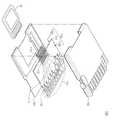
도 1은 본 발명의 실시 예에 따른 메모리 카드 어댑터를 예시적으로 보여주는 도면이다. 도 1을 참조하면, 메모리 카드 어댑터(100)는 메모리 카드(10)를 물리적으로 삽입하고 패키지 기판(package substrate, 110)을 고정하는 하부 리드(bottom lid, 101), 및 패키지 기판(110)을 감싸안고 하부 리드(101)와 결합으로써 하우징을 구성하는 상부 리드(top lid, 102)를 포함한다.
실시 예에 있어서, 메모리 카드(10)는 마이크로 SD(secure digital) 카드일 수 있다. 하지만, 본 발명의 메모리 카드(10)가 마이크로 SD 카드에 제한될 필요는 없다. 본 발명의 메모리 카드(10)는 다양한 종류의 메모리 카드일 수 있다. 아래에서는 설명의 편의를 위하여 메모리 카드(10)가 마이크로 SD 카드라고 하겠다.
패키지 기판(110)은 메모리 카드(10)와 외부의 카드 소켓을 전기적으로 연결한다. 패키지 기판(110)은 제 1 면과 제 2 면을 갖는 코어(111), 제 1 면에 형성된 제 1 레이어(first layer, 110a), 제 2 면에 형성된 제 2 레이어(second layer, 110b), 및 접촉핀들(113)을 포함한다.
코어(111)는 절연 물질을 포함할 것이다. 예를 들어, 코어(111)는 글래스 에폭시로 구현될 수 있다.
제 1 레이어(110a)는 접촉핀들(113)이 결합되는 접촉 랜드들(112)을 포함한다. 접촉 랜드들(112)은 배선들(115) 및 비아홀들(115)을 통하여 접촉 패드들(114)에 전기적으로 연결될 것이다. 배선들(115)은 제 1 레이어(110a)에 형성된 제 1 배선들과 제 2 레이어(110b)에 형성된 제 2 배선들을 구분될 수 있다. 여기서 제 1 배선들은 접촉 랜드들(112)과 대응하는 비아홀들(115)을 연결하고, 제 2 배선들은 접촉 패드들(114)와 대응하는 비하홀들(115)을 연결할 것이다.
도 1에 도시된 바와 같이 배선들(115) 각각은 랜드들(112)/패드들(114)과 비하홀들(115) 사이에서 최단 거리인 직선(straight line) 형태로 구현될 수 있다. 하지만, 본 발명의 배선들(115)이 반드시 직선 형태로 구현될 필요는 없다. 데이터 스큐(skew)를 맞추기 위해서 배선들(115)의 모양 및 길이는 다양한 형태로 구현가능하다.
실시 예에 있어서, 제 1 레이어(110a)는 적어도 하나의 신호 라인(예를 들어, DAT0, DAT1, DAT2, DAT3, CMD, CLK)에 대한 리턴 패스를 구비할 수 있다. 여기서 리턴 패스는 전원 패드(VDD) 혹은 접지 패드(VSS1/VSS2)에 대응하는 접촉 랜드에 연결된 평면 형태의 전도 영역일 수 있다.
제 2 레이어(110b)는 카드 소켓에 접촉하는 접촉 패드들(114)을 포함한다. 실시 예에 있어서, 접촉 패드들(114) 각각의 크기는 대응하는 접촉 랜드들(112) 각각의 크기보다 크다. 실시 예에 있어서, 제 2 레이어(110b)는 적어도 하나의 신호 라인(예를 들어, DAT0, DAT1, DAT2, DAT3, CMD, CLK)에 대한 리턴 패스(도시되지 않음)를 구비할 수 있다. 여기서 리턴 패스는 전원 패드(VDD) 혹은 접지 패드(VSS1/VSS2)에 연결된 평면 형태의 전도 영역일 수 있다.
실시 예에 있어서, 패키지 기판(110)은 인쇄 회로 기판(printed circuit board; PCB)로 구현될 수 있다.
실시 예에 있어서 메모리 카드 어댑터(100)는 UHS(ultra high speed) 전용 어댑터일 수 있다.
도 1에서 패키지 기판(110)은 레이어들(110a, 110b)을 이용하여 신호 라인(DAT0~DAT3, CMD, CLK)의 라우팅(routing)을 구현하였다. 그러나 본 발명의 패키지 기판(110)의 레이어들이 반드시 2개에 제한될 필요는 없다. 본 발명의 실시 예에 따른 패키지 기판은 라우팅을 하기 위하여 적어도 3개의 레이어들을 포함할 수도 있다.
일반적인 핀-투-핀(pin-to-pin) 구조의 메모리 카드 어댑터는 어느 하나의 신호 라인의 리턴 패스가 인접한 다른 신호 라인이 되기 때문에, 고속의 메모리 카드에 적합하지 않다. 또한, 일반적인 메모리 카드 어댑터는 데이터 핀(DAT0~DAT3)의 물리적인 위치에 대한 한계에 따라 데이터 스큐를 맞추기도 어렵다.
반면에, 본 발명의 실시 예에 따른 메모리 카드 어댑터(100)는 어느 하나의 신호 라인의 리턴 패스가 인접한 신호 라인이 되지 않게 하기 위하여 별도의 리턴 패스를 갖는 패키지 기판(110)를 구비함으로써, 고속의 카드 동작에 적합하다. 게다가, 본 발명의 실시 에에 따른 메모리 카드 어댑터(100)는 복수의 레이어들(110a, 110b)을 구비함으로써, 자유롭게 신호 라인의 라우팅을 수행할 수 있다. 이에 따라 신호 라인의 데이터 스큐가 쉽게 맞춰질 수 있다.
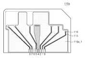
도 2는 도 1에 도시된 패키지 기판(110)의 제 1 레이어(110a)를 예시적으로 보여주는 도면이다. 도 2를 참조하면, 제 1 레이어(110a)는 리턴 패스로 이용되는 평면 형태의 도전 영역(110a_1)을 포함한다. 여기서 도전 영역(110a_1)은 제 1 접지 패드(VSS1) 혹은 제 2 접지 패드(VSS2)에 대응하는 접촉 랜드(6)에 전기적으로 연결된다. 도 2에 도시된 바와 같이, 도전 영역(110a_1)은 제 2 레이어(110b)의 신호 패드들(DAT0 ~ DAT3, CMD, CLK)에 대칭되는 영역들에 형성되지 않을 것이다.
데이터 패드들(DAT0 ~DAT3), 커맨드 패드(CMD), 및 클록 패드(CLK) 대응하는 접촉 랜드들(8, 7, 5, 2, 1, 9) 각각은 배선을 통하여 비아홀에 전기적으로 연결될 것이다. 한편, 전원 패드(VDD)에 대응하는 접촉 랜드(4)는 배선을 통하여 복수의 비아홀들에 전기적으로 연결될 수 있다.
도 3은 도 1에 도시된 패키지 기판(110)의 제 2 레이어(110b)를 예시적으로 보여주는 도면이다. 도 3을 참조하면, 제 2 레이어(110b)는 리턴 패스로 이용되는 평면 형태의 도전 영역(110b_1)을 포함한다. 여기서 도전 영역(110b_1)은 제 1 접지 패드(VSS1) 및 제 2 접지 패드(VSS2)에 전기적으로 연결된다. 데이터 패드들(DAT0 ~DAT3), 커맨드 패드(CMD), 및 클록 패드(CLK) 각각은 배선을 통하여 비아홀에 연결되거나 배선없이 직접 비아홀에 연결될 수 있다. 전원 패드(VDD)는 배선들을 통하여 복수의 비아홀들에 연결되거나 배선없이 비아홀들에 직접 연결될 수 있다.
실시 예에 있어서, 제 2 레이어(110b)의 도전 영역(110b_1)은 제 1 레이어(110a)의 도전 영역(110a_1)과 복수의 비아홀들(도시되지 않음)을 통하여 전기적으로 연결될 수 있다.
도 3에서 리턴 패스로 이용되는 도전 영역(110b_1)은 접지 패드들(VSS1/VSS2)에 연결되었다. 하지만, 본 발명이 반드시 여기에 제한될 필요는 없다. 리턴 패스로 이용되는 도전 영역은 전원 패드(VDD)에 연결될 수도 있다.
한편, 본 발명의 실시 예에 따른 패키지 기판은 데이터와 클록의 동기를 위하여 수동 소자(passive device)를 더 구비할 수 있다.
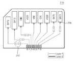
도 4는 본 발명에 따른 패키지 기판에 대한 제 2 실시 예를 예시적으로 보여주는 도면이다. 도 4를 참조하면, 패키지 기판(210)은 도 1에 도시된 패키지 기판(110)와 비교하여, 데이터 패드들(DAT0~DAT3) 및 커맨드 패드(CMD) 각각에 연결된 신호 라인에 수동 소자(passive element, 217)를 더 포함한다. 수동 소자(217)는 데이터 패드들(DAT0~DAT3) 및 커맨드 패드(CMD) 각각에 입력되는 신호와 클록 패드(CLK)에 입력되는 클록과 동기를 위하여 저항 성분/인덕터 성분/커패시터성분의 보상을 수행할 수 있다. 실시 예에 있어서 수동 소자(217)는 패키지 기판(210)의 제 1 면(예를 들어, 도 2의 제 1 레이어(110a))에 배치될 수 있다.
본 발명의 실시 예에 따른 패키지 기판(210)은, 적어도 하나의 신호 라인에 적어도 하나의 수동 소자(217)를 연결시킴으로써, 저항/인덕터/커패시터를 최적의 조건으로 조절/가변/조정/변화시킬 수 있다.
한편, 본 발명의 실시 예에 따른 패키지 기판은 각 데이터의 스큐를 맞추기 위하여 신호 길이를 조절하기 위하여 제 1 및 제 2 레이어 사이에서 다양한 방법으로 라우팅할 수 있다.
도 5는 본 발명에 따른 패키지 기판에 대한 제 3 실시 예를 예시적으로 보여주는 도면이다. 도 5를 참조하면, 패키지 기판(310)은 데이터 스큐를 맞추기 위하여 비아홀들을 이용한 물리적인 라우팅을 통하여 데이터 패드들(DAT0~DAT3) 각각의 신호 길이를 조절할 수 있다.
아래에서는 데이터 패드(DAT1)에 대응하는 신호 라인을 설명하겠다. 제 2 레이어(예를 들어, 도 3의 110b)의 데이터 패드(DAT1)와 제 1 레이어(예를 들어, 도 2의 110a)의 접촉 랜드(8)가 전기적으로 연결되기 위해서는 3개의 비아홀들(316_1, 316_2, 316_3)과 4개의 배선들(315_1, 315_2, 315_3, 315_4)이 이용된다. 제 1 배선(315_1)은 데이터 패드(DAT1)와 제 1 비아홀(316_1)을 연결하기 위하여 제 2 레이어(110b)에 형성되고, 제 2 배선(315_2, 점선처리)은 제 1 비아홀(316_1)과 제 2 비아홀(316_2)를 연결하기 위하여 제 1 레이어(110a)에 형성되고, 제 3 배선(315_3)은 제 2 비아홀(316_2)과 제 3 비아홀(316_3)를 연결하기 위하여 제 2 레이어(110b)에 형성되고, 제 4 배선(315_4, 점선처리)은 제 3 비아홀(316_3)과 접촉 랜드(8)를 연결하기 위하여 제 1 레이어(110a)에 형성될 것이다.
본 발명의 실시 예에 따른 패키지 기판(310)은 적어도 2개의 비아홀들을 이용하여 신호 패드(DAT0/DAT1/DAT2/DAT3/CMD/CLK)와 대응하는 접촉 랜드를 연결함으로써 신호 길이를 조절할 수 있다.
한편, 본 발명의 실시 예에 따른 패키지 기판은 신호 패드와 대응하는 접촉 랜드를 연결하기 위하여 복수의 신호 라인들을 구비하고, 필요에 따라 복수의 신호 라인들 중 어느 하나를 통하여 신호 패드와 대응하는 접촉 랜드를 연결할 수도 있다.
도 6은 본 발명에 따른 패키지 기판에 대한 제 4 실시 예를 예시적으로 보여주는 도면이다. 도 6를 참조하면, 패키지 기판(410)은 데이터 패드들(DAT0~DAT3) 각각이 대응하는 접촉 랜드를 연결하기 위하여 복수의 신호 라인들(SL1, SL2, SL3)을 구비한다. 여기서 신호 라인들(SL1, SL2, SL3) 각각은 고주파 신호에 따라 서로 다른 신호 특성을 갖도록 패키지 기판(410)에 형성될 것이다. 도 6에 형성된 신호 라인들(SL1, SL2, SL3)의 개수는 3개이지만, 본 발명은 여기에 제한되지 않을 것이다.
메모리 카드 어댑터(100, 도 1 참조)의 제조자는 복수의 신호 라인들(SL1, SL2, SL3) 중에서 메모리 카드 어댑터(100, 도 1 참조)가 수용될 제품의 특성에 적합한 신호 라인을 선택하고, 선택된 신호 라인을 이용하여 데이터 패드와 대응하는 접촉 랜드를 연결할 것이다.
본 발명의 실시 예에 따른 패키지 기판(410)은 제품에 적합한 신호 라인을 선택적으로 연결할 수 있다.
도 1에 도시된 접촉 핀들(113)은 패키지 기판(110)로부터 도출된 모양이었다. 그러나 본 발명의 접촉 핀들이 반드시 이렇게 구현될 필요는 없다. 본 발명의 접촉 핀들은 패키지 기판의 코어에 형성된 홈에 구현될 수 있다.
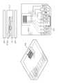
도 7은 본 발명에 따른 패키지 기판에 대한 제 5 실시 예를 예시적으로 보여주는 도면이다. 도 7을 참조하면, 패키지 기판(510)은 접촉 핀들(512)이 PCB 모듈의 홈(518)에 구비될 것이다. 접촉 핀들(512) 각각은 접촉 핀(512_1)과 고정 패드(512_2)를 포함할 것이다. 도 7에 도시된 바와 같이 PCB 모듈, 즉 패키지 기판(510)은 하부 리드(501)과 상부 리드(502)에 의해 감싸진다. 마이크로 카드(10)가 PCB 모듈(510)의 홈(518)에 삽입됨으로써 마이크로 카드(10)와 PCB 모듈의 홈(518)에 형성된 접촉 핀들(512)이 전기적으로 연결될 것이다.
도시되지 않았지만, 클록와 데이터의 동기 혹은 데이터 스큐를 맞추기 위하여 패키지 기판(510)의 접촉 패드들 중 적어도 하나에 연결된 라인은 적어도 하나의 비아홀을 통하여 라우팅되거나, 적어도 하나의 수동 소자에 연결될 수 있다.
본 발명은 핀-투-핀 구조의 메모리 카드 어댑터에도 적용 가능하다.
도 8은 본 발명에 따른 핀-투-핀 구조의 메모리 카드 어댑터에 대한 제 1 실시 예를 예시적으로 보여주는 도면이다. 도 8를 참조하면, 메모리 카드 어댑터(600)는 핀-투-핀 구조의 핀들(611), 절연판(612) 및 도전판(613)을 포함한다. 핀들(611) 위에 절연판(612)이 존재하고, 절연판(612) 위에 도전판(613)이 존재한다. 여기서 도전판(613)은 핀들(611) 중 접지핀(VSS2)에 연결될 것이다. 도전판(613)은 신호 라인에 대한 리턴 패스로 이용될 것이다. 다른 실시 예에 있어서, 도전판(613)은 전원핀(VDD)에 연결될 수도 있다.
실시 에에 있어서, 절연판(612) 및 도전판(613) 각각은 필름 형태로 구현될 수 있다.
도 8에서 절연판(612)및 도전판(613)은 핀들(611) 위에 배치되었다. 그러나 본 발명이 여기에 제한될 필요는 없다. 절연판과 도전판은 핀들 아래에 배치될 수 있다.
도 9는 본 발명에 따른 핀-투-핀 구조의 메모리 카드 어댑터에 대한 제 2 실시 예를 예시적으로 보여주는 도면이다. 도 9를 참조하면, 메모리 카드 어댑터(700)는 핀-투-핀 구조의 핀들(711), 핀들(711) 아래에 배치된 절연판(712) 및 절연판(712) 아래에 배치된 도전판(713)을 포함한다.
또한, 절연판과 도전판은 핀들로 기준으로 상하에 배치될 수도 있다.
도 10은 본 발명에 따른 핀-투-핀 구조의 메모리 카드 어댑터에 대한 제 3 실시 예를 예시적으로 보여주는 도면이다. 도 10을 참조하면, 메모리 카드 어댑터(800)는 핀-투-핀 구조의 핀들(811), 핀들(811) 위에 배치된 제 1 절연판(812) 및 제 1 절연판(812) 위에 배치된 제 1 도전판(813), 핀들(811) 아래에 배치된 제 2 절연판(814) 및 제 2 절연판(814) 아래에 배치된 제 2 도전판(815)을 포함한다.
도 1 내지 도 10에서 도시된 리턴 패스로 이용되는 도전 영역은 기판 형태이다. 그러나, 본 발명의 리턴 패스를 형성하는 구조가 반드시 여기에 제한될 필요는 없다. 본 발명의 실시 예에 따른 메모리 카드 어댑터는 신호 라인의 리턴 패스를 갖는 어떠한 형태의 구조 및 방법으로 구현될 수 있다.
한편, 상술 된 본 발명의 내용은 발명을 실시하기 위한 구체적인 실시 예들에 불과하다. 본 발명은 구체적이고 실제로 이용할 수 있는 수단 자체뿐 아니라, 장차 기술로 활용할 수 있는 추상적이고 개념적인 아이디어인 기술적 사상을 포함할 것이다.BRIEF DESCRIPTION OF THE DRAWINGS The above and other objects, features and advantages of the present invention will be more apparent from the following detailed description taken in conjunction with the accompanying drawings, in which: FIG.
The memory card adapter according to the embodiment of the present invention is suitable for high-frequency characteristics by having a return path to the signal line. Here, the return path is a path having a low impedance through which the current induced by the high-frequency signal flows so as not to affect the signal line. In general, a current induced by a high frequency signal has a characteristic of flowing to a low impedance region.
1 is an exemplary illustration of a memory card adapter according to an embodiment of the present invention. 1, a
In an embodiment, the
The
The
The
As shown in FIG. 1, each of the
In an embodiment, the
The
In an embodiment, the
In an embodiment, the
1, the
A memory card adapter having a general pin-to-pin structure is not suitable for a high-speed memory card because the return path of any one of the signal lines becomes another adjacent signal line. In addition, it is difficult for a general memory card adapter to adapt the data skew to the limits of the physical positions of the data pins DAT0 to DAT3.
On the other hand, the
FIG. 2 is a view illustrating an exemplary
Each of the contact lands 8, 7, 5, 2, 1, 9 corresponding to the data pads DAT0 to DAT3, the command pad CMD, and the clock pad CLK is electrically connected to the via- . Meanwhile, the
FIG. 3 is a view illustrating an exemplary
In an embodiment, the conductive region 110b_1 of the
In Fig. 3, the conductive region 110b_1 used as a return path is connected to the ground pads VSS1 / VSS2. However, the present invention is not necessarily limited thereto. A conductive region used as a return path may be connected to the power supply pad VDD.
Meanwhile, the package substrate according to the embodiment of the present invention may further include a passive device for synchronizing data and a clock.
4 is a view illustrating an example of a second embodiment of a package substrate according to the present invention. 4, the
The
Meanwhile, the package substrate according to the embodiment of the present invention may be routed in various ways between the first and second layers in order to adjust the signal length in order to adjust the skew of each data.
5 is a view illustrating an example of a third embodiment of the package substrate according to the present invention. Referring to FIG. 5, the
Hereinafter, a signal line corresponding to the data pad DAT1 will be described. In order for the data pad DAT1 of the second layer (for example, 110b in FIG. 3) and the
The
Meanwhile, the package substrate according to the embodiment of the present invention includes a plurality of signal lines for connecting the signal pads and the corresponding contact lands, and may be connected to the corresponding signal pads through any one of the plurality of signal lines, You can also connect the land.
6 is a view illustrating an example of a fourth embodiment of the package substrate according to the present invention. Referring to FIG. 6, the
The manufacturer of the memory card adapter 100 (see Fig. 1) selects a signal line suited to the characteristics of the product to be accommodated by the memory card adapter 100 (see Fig. 1) among the plurality of signal lines SL1, SL2, The selected signal line will be used to connect the data pad to the corresponding contact land.
The
The contact pins 113 shown in FIG. 1 were derived from the
7 is a view illustrating an exemplary fifth embodiment of a package substrate according to the present invention. Referring to FIG. 7, the
Although not shown, a line connected to at least one of the contact pads of the
The present invention is also applicable to a memory card adapter having a pin-to-pin structure.
FIG. 8 is an exemplary view showing a first embodiment of a memory card adapter of a pin-to-pin structure according to the present invention. 8, the
In the embodiment, each of the insulating plate 612 and the
In Fig. 8, the insulating plate 612 and the
FIG. 9 is a view showing a second embodiment of a memory card adapter of a pin-to-pin structure according to the present invention. 9, the
Further, the insulating plate and the conductive plate may be disposed on the upper and lower sides with reference to the pins.
10 is an exemplary view showing a third embodiment of a memory card adapter of a pin-to-pin structure according to the present invention. 10, the
The conductive region used in the return path shown in Figs. 1 to 10 is in the form of a substrate. However, the structure for forming the return path of the present invention is not necessarily limited thereto. A memory card adapter according to an embodiment of the present invention may be implemented in any type of structure and method with a return path of a signal line.
The above-described contents of the present invention are only specific examples for carrying out the invention. The present invention will include not only concrete and practical means themselves, but also technical ideas which are abstract and conceptual ideas that can be utilized as future technologies.
100: 메모리 카드 어댑터
110: 패키지 기판
110a: 제 1 레이어
110b: 제 2 레이어
111: 코어
112: 접촉 랜드들
114: 접촉 패드들
115: 배선
116: 비아홀
117: 수동 소자100: Memory card adapter
110: package substrate
110a: First layer
110b: second layer
111: Core
112: contact lands
114: contact pads
115: Wiring
116: via hole
117: Passive element
Claims (18)
Translated fromKorean패키지 기판을 포함하고,
상기 하우징은:
하부 리드; 및
상기 하부 리드와 함게 상기 하우징을 형성하는 상부 리드를 포함하고,
상기 패키지 기판은 상기 하부 리드 및 상기 상부 리드 사이에 배치되고, 상기 하부 리드에 고정되고,
상기 패키지 기판은:
제1면 및 제2면을 갖는 코어;
상기 제1면 위에 배치되고 복수의 접촉 랜드들을 포함하는 제1 레이어; 그리고
상기 제2면 위에 배치되고 상기 코어를 관통하는 비아홀들을 통하여 상기 접촉 랜드들에 전기적으로 연결되는 접촉 패드들을 포함하는 제 2 레이어를 포함하고,
상기 제1 레이어 및 상기 제2 레이어 중 하나는 적어도 하나의 신호 라인에 대한 리턴 패스로 동작하는 도전 영역을 포함하고,
상기 도전 영역은 배선이 배치되는 적어도 하나의 채널을 정의하고,
상기 배선은 상기 접촉 랜드들 또는 상기 접촉 패드들 중 하나를 상기 비아홀들 중 하나와 전기적으로 연결하고,
상기 패키지 기판은 인쇄 회로 기판인 메모리 카드 어댑터.A housing configured to insert a memory card; And
A package substrate,
Said housing comprising:
A lower lead; And
And an upper lead forming the housing together with the lower lead,
Wherein the package substrate is disposed between the lower lead and the upper lead, and is fixed to the lower lead,
Wherein the package substrate comprises:
A core having a first side and a second side;
A first layer disposed over the first surface and including a plurality of contact lands; And
And a second layer disposed on the second surface and including contact pads electrically connected to the contact lands through via holes passing through the core,
Wherein one of the first layer and the second layer includes a conductive region that operates as a return path for at least one signal line,
Wherein the conductive region defines at least one channel in which the wiring is disposed,
The wiring electrically connecting one of the contact lands or the contact pads with one of the via holes,
Wherein the package substrate is a printed circuit board.
상기 패키지 기판의 홈에 구현되는 접촉 핀들을 더 포함하고,
상기 접촉 핀들은 메모리 카드와 상기 접촉 랜드들을 전기적으로 연결하는 메모리 카드 어댑터.The method according to claim 1,
Further comprising contact pins implemented in the grooves of the package substrate,
Wherein the contact pins electrically connect the memory card and the contact lands.
상기 패키지 기판에 도출된 접촉 핀들을 더 포함하고,
상기 접촉 핀들은 메모리 카드와 상기 접촉 랜드들을 전기적으로 연결하는 메모리 카드 어댑터.The method according to claim 1,
Further comprising contact pins derived from the package substrate,
Wherein the contact pins electrically connect the memory card and the contact lands.
상기 복수의 접촉 패드들은 상기 비아홀들에 배선없이 직접 전기적으로 연결되는 메모리 카드 어댑터.The method according to claim 1,
Wherein the plurality of contact pads are directly electrically connected to the via holes without wiring.
상기 제1 레이어는 상기 접촉 랜드들과 상기 비아홀들 사이의 제1 배선들을 포함하고, 상기 제1 배선들의 각 배선은 상기 복수의 접촉 랜드들 중 하나에 대응하고,
상기 제2 레이어는 상기 비아홀들과 상기 접촉 패드들 사이의 제2 배선들을를 포함하고, 상기 제2 배선들의 각 배선은 상기 복수의 접촉 패드들 중 하나에 대응하는 메모리 카드 어댑터.The method according to claim 1,
Wherein the first layer includes first wirings between the contact lands and the via holes, each wiring of the first wirings corresponds to one of the plurality of contact lands,
Wherein the second layer includes second interconnections between the via holes and the contact pads, and each interconnect of the second interconnections corresponds to one of the plurality of contact pads.
상기 제1 배선들 중 적어도 하나 또는 상기 제2 배선들 중 적어도 하나는 직선 형태로 구현되는 메모리 카드 어댑터.6. The method of claim 5,
Wherein at least one of the first wirings or the second wirings is implemented in a straight line shape.
상기 제2 레이어는 상기 도전 영역을 포함하고, 상기 도전 영역은 사각형을 갖는 메모리 카드 어댑터.The method according to claim 1,
The second layer includes the conductive region, and the conductive region has a rectangular shape.
상기 도전 영역은 전원 패드와 연결되고, 상기 전원 패드는 상기 복수의 접촉 패드들 중 하나인 메모리 카드 어댑터.8. The method of claim 7,
Wherein the conductive region is connected to a power supply pad, and the power supply pad is one of the plurality of contact pads.
상기 도전 영역은 접지 패드와 연결되고, 상기 접지 패드는 상기 복수의 접촉 패드들 중 하나인 메모리 카드 어댑터.8. The method of claim 7,
The conductive region is connected to a ground pad, and the ground pad is one of the plurality of contact pads.
상기 제2 레이어는 평면 형태의 대응하는 제2 도전 영역을 포함하고,
상기 도전 영역은 상기 리턴 패스로 동작하는 상기 제1 레이어에 대응하고,
상기 제2 레이어에 대응하는 상기 제2 도전 영역 및 상기 제1 레이어에 대응하는 상기 도전 영역은 상기 복수의 비아홀들을 통해 전기적으로 연결되는 메모리 카드 어댑터.The method according to claim 1,
The second layer comprising a corresponding second conductive region in planar form,
The conductive region corresponding to the first layer operating with the return path,
Wherein the second conductive region corresponding to the second layer and the conductive region corresponding to the first layer are electrically connected through the plurality of via holes.
상기 복수의 비아홀들 중에서 적어도 2개의 비아홀들은 적어도 하나의 신호 패드와 전기적으로 연결되고, 상기 적어도 하나의 신호 패드는 상기 복수의 접촉 패드들 중 하나이고, 상기 적어도 2개의 비아 홀들은 상기 신호 패드에 전기적으로 연결되는 메모리 카드 어댑터.The method according to claim 1,
At least two via holes among the plurality of via holes are electrically connected to at least one signal pad, the at least one signal pad is one of the plurality of contact pads, and the at least two via holes are connected to the signal pad A memory card adapter that is electrically connected.
상기 복수의 접촉 랜드들 중 하나와 연결되는 상기 제1면 상의 제1 배선들; 그리고
전원 패드와 연결되는 상기 제2면 상의 제2 배선들을 더 포함하고,
상기 복수의 비아홀들은 상기 제1 배선들 및 상기 제2 배선들을 연결하는 메모리 카드 어댑터.12. The method of claim 11,
First wirings on the first surface connected to one of the plurality of contact lands; And
And second wirings on the second surface connected to the power supply pad,
And the plurality of via holes connect the first wires and the second wires.
상기 적어도 하나의 신호 라인과 연결되는 상기 제2면 상의 적어도 하나의 수동 소자를 더 포함하는 메모리 카드 어댑터.The method according to claim 1,
Further comprising at least one passive element on the second side coupled to the at least one signal line.
접지 핀을 포함하는 복수의 핀-투-핀 구조의 핀들;
상기 복수의 핀-투-핀 구조의 핀들 상의 절연판; 및
도전판을 포함하고,
상기 도전판 및 상기 절연판은 상기 하우징과 유사한 형태를 갖는 메모리 카드 어댑터.housing;
A plurality of pins of a pin-to-pin structure including a ground pin;
An insulating plate on the plurality of pins of the pin-to-pin structure; And
Comprising a conductive plate,
Wherein the conductive plate and the insulating plate have a shape similar to the housing.
상기 복수의 핀-투-핀 구조의 핀들은 전원 핀을 포함하고,
상기 도전판은 상기 전원 핀에 연결되는 메모리 카드 어댑터.15. The method of claim 14,
Wherein the plurality of pins of the pin-to-pin structure include power pins,
And the conductive plate is connected to the power pin.
상기 도전판은 상기 접지 핀 그리고 상기 접지 핀에 대응하는 상기 복수의 핀-투-핀 구조의 핀들 중 다른 하나의 핀 중에서 하나와 연결되는 메모리 카드 어댑터.15. The method of claim 14,
Wherein the conductive plate is connected to one of the pins of the other of the plurality of pin-to-pin structures corresponding to the ground pin and the ground pin.
상기 복수의 핀-투-핀 구조의 핀들 상의 제1 절연판;
상기 접지 핀과 연결되고, 적어도 하나의 신호 라인에 대한 리턴 패스로 동작하는 상기 제1 절연판 상의 제1 도전판;
상기 복수의 핀-투-핀 구조의 핀들 아래의 제2 절연판; 그리고
상기 접지 핀과 연결되고, 적어도 다른 하나의 신호 라인에 대한 리턴 패스로 동작하는 상기 제2 절연판 아래의 제2 도전판을 포함하고,
상기 제1 도전판 및 상기 제1 절연판은 유사한 제1 형태를 갖고, 그리고
상기 제2 도전판 및 상기 제2 절연판은 유사한 제2 형태를 갖는 메모리 카드 어댑터.A plurality of pins of a pin-to-pin structure including a ground pin;
A first insulating plate on the pins of the plurality of pin-to-pin structures;
A first conductive plate on the first insulating plate, which is connected to the ground pin and operates as a return path for at least one signal line;
A second insulating plate under the pins of the plurality of pin-to-pin structures; And
And a second conductive plate connected to the ground pin and under the second insulating plate operating with a return path for at least another signal line,
The first conductive plate and the first insulating plate have a similar first shape, and
Wherein the second conductive plate and the second insulating plate have a similar second shape.
패키지 기판을 포함하고,
상기 하우징은:
하부 리드; 및
상기 하부 리드와 함게 상기 하우징을 형성하는 상부 리드를 포함하고,
상기 패키지 기판은 상기 하부 리드 및 상기 상부 리드 사이에 배치되고, 상기 하부 리드에 고정되고,
상기 패키지 기판은:
제1면 및 제2면을 갖는 코어;
상기 제1면 위에 배치되고 복수의 접촉 랜드들을 포함하는 제1 레이어; 그리고
상기 제2면 위에 배치되고 상기 코어를 관통하는 비아홀들을 통하여 상기 접촉 랜드들에 전기적으로 연결되는 접촉 패드들을 포함하는 제 2 레이어를 포함하고,
상기 제1 레이어 및 상기 제2 레이어 중 하나는 적어도 하나의 신호 라인에 대한 리턴 패스로 동작하는 도전 영역을 포함하고,
상기 도전 영역은 배선이 아니고, 상기 접촉 랜드들 및 상기 접촉 패드들과 구별되고, 그리고 상기 제1 레이어 및 상기 제2 레이어 중 하나의 과반을 덮는 메모리 카드 어댑터.A housing configured to insert a memory card; And
A package substrate,
Said housing comprising:
A lower lead; And
And an upper lead forming the housing together with the lower lead,
Wherein the package substrate is disposed between the lower lead and the upper lead, and is fixed to the lower lead,
Wherein the package substrate comprises:
A core having a first side and a second side;
A first layer disposed over the first surface and including a plurality of contact lands; And
And a second layer disposed on the second surface and including contact pads electrically connected to the contact lands through via holes passing through the core,
Wherein one of the first layer and the second layer includes a conductive region that operates as a return path for at least one signal line,
Wherein the conductive region is not a wire but is distinguished from the contact lands and the contact pads and covers one half of the first layer and the second layer.
Priority Applications (7)
| Application Number | Priority Date | Filing Date | Title |
|---|---|---|---|
| KR1020120125782AKR101893032B1 (en) | 2012-11-08 | 2012-11-08 | Memory card adapter |
| US13/953,967US9202160B2 (en) | 2012-11-08 | 2013-07-30 | Memory card adapter |
| CN201310551907.2ACN103811955B (en) | 2012-11-08 | 2013-11-08 | Adapter for IC card |
| TW102140600ATWI586054B (en) | 2012-11-08 | 2013-11-08 | Memory card adapter |
| KR1020140029122AKR20150014840A (en) | 2012-11-08 | 2014-03-12 | Memory card adapter |
| US14/643,034US9722653B2 (en) | 2012-11-08 | 2015-03-10 | Memory card adapter |
| US15/404,707US9882327B2 (en) | 2012-11-08 | 2017-01-12 | Memory card adapter |
Applications Claiming Priority (1)
| Application Number | Priority Date | Filing Date | Title |
|---|---|---|---|
| KR1020120125782AKR101893032B1 (en) | 2012-11-08 | 2012-11-08 | Memory card adapter |
Publications (2)
| Publication Number | Publication Date |
|---|---|
| KR20140059388A KR20140059388A (en) | 2014-05-16 |
| KR101893032B1true KR101893032B1 (en) | 2018-10-04 |
Family
ID=50622766
Family Applications (2)
| Application Number | Title | Priority Date | Filing Date |
|---|---|---|---|
| KR1020120125782AActiveKR101893032B1 (en) | 2012-11-08 | 2012-11-08 | Memory card adapter |
| KR1020140029122AWithdrawnKR20150014840A (en) | 2012-11-08 | 2014-03-12 | Memory card adapter |
Family Applications After (1)
| Application Number | Title | Priority Date | Filing Date |
|---|---|---|---|
| KR1020140029122AWithdrawnKR20150014840A (en) | 2012-11-08 | 2014-03-12 | Memory card adapter |
Country Status (4)
| Country | Link |
|---|---|
| US (1) | US9202160B2 (en) |
| KR (2) | KR101893032B1 (en) |
| CN (1) | CN103811955B (en) |
| TW (1) | TWI586054B (en) |
Families Citing this family (46)
| Publication number | Priority date | Publication date | Assignee | Title |
|---|---|---|---|---|
| KR20100030126A (en) | 2008-09-09 | 2010-03-18 | 삼성전자주식회사 | Memory device and electronic apparatus comprising the same |
| USD794641S1 (en)* | 2009-01-07 | 2017-08-15 | Samsung Electronics Co., Ltd. | Memory device |
| USD794643S1 (en)* | 2009-01-07 | 2017-08-15 | Samsung Electronics Co., Ltd. | Memory device |
| USD794644S1 (en)* | 2009-01-07 | 2017-08-15 | Samsung Electronics Co., Ltd. | Memory device |
| USD794642S1 (en)* | 2009-01-07 | 2017-08-15 | Samsung Electronics Co., Ltd. | Memory device |
| USD795262S1 (en)* | 2009-01-07 | 2017-08-22 | Samsung Electronics Co., Ltd. | Memory device |
| USD794034S1 (en)* | 2009-01-07 | 2017-08-08 | Samsung Electronics Co., Ltd. | Memory device |
| USD795261S1 (en)* | 2009-01-07 | 2017-08-22 | Samsung Electronics Co., Ltd. | Memory device |
| US9442539B2 (en) | 2013-04-05 | 2016-09-13 | Pny Technologies, Inc. | Reduced length memory card |
| USD734755S1 (en)* | 2013-06-26 | 2015-07-21 | Samsung Electronics Co., Ltd. | Solid state drive |
| USD735204S1 (en)* | 2013-06-26 | 2015-07-28 | Samsung Electronics Co., Ltd. | Solid state drive |
| USD735202S1 (en)* | 2013-06-26 | 2015-07-28 | Samsung Electronics Co., Ltd. | Solid state drive |
| USD735203S1 (en)* | 2013-06-26 | 2015-07-28 | Samsung Electronics Co., Ltd. | Solid state drive |
| USD734756S1 (en)* | 2014-04-04 | 2015-07-21 | Pny Technologies, Inc. | Reduced length memory card |
| USD730907S1 (en)* | 2014-05-02 | 2015-06-02 | Samsung Electronics Co., Ltd. | Memory card |
| USD730910S1 (en)* | 2014-05-02 | 2015-06-02 | Samsung Electronics Co., Ltd. | Memory card |
| USD730908S1 (en)* | 2014-05-02 | 2015-06-02 | Samsung Electronics Co., Ltd. | Memory card |
| USD730911S1 (en)* | 2014-05-02 | 2015-06-02 | Samsung Electronics Co., Ltd. | Memory card |
| USD729251S1 (en)* | 2014-06-27 | 2015-05-12 | Samsung Electronics Co., Ltd. | Memory card |
| USD727913S1 (en)* | 2014-06-27 | 2015-04-28 | Samsung Electronics Co., Ltd. | Memory card |
| USD730909S1 (en)* | 2014-06-27 | 2015-06-02 | Samsung Electronics Co., Ltd. | Memory card |
| USD727911S1 (en)* | 2014-06-27 | 2015-04-28 | Samsung Electronics Co., Ltd. | Memory card |
| USD727912S1 (en)* | 2014-06-27 | 2015-04-28 | Samsung Electronics Co., Ltd. | Memory card |
| USD728577S1 (en)* | 2014-07-01 | 2015-05-05 | Google Inc. | Mobile device module |
| USD736215S1 (en)* | 2014-07-01 | 2015-08-11 | Samsung Electronics Co., Ltd. | Memory card |
| USD736212S1 (en)* | 2014-07-01 | 2015-08-11 | Samsung Electronics Co., Ltd. | Memory card |
| USD736214S1 (en)* | 2014-07-01 | 2015-08-11 | Samsung Electronics Co., Ltd. | Memory card |
| USD730906S1 (en)* | 2014-07-01 | 2015-06-02 | Google Inc. | Mobile device module |
| KR102284653B1 (en) | 2014-07-02 | 2021-08-03 | 삼성전자 주식회사 | Electronic device |
| USD727910S1 (en)* | 2014-07-02 | 2015-04-28 | Samsung Electronics Co., Ltd. | Memory card |
| USD877147S1 (en)* | 2014-07-04 | 2020-03-03 | Sakai Display Products Corporation | Image display |
| USD873822S1 (en)* | 2014-07-04 | 2020-01-28 | Sakai Display Products Corporation | Image display |
| CN105676949B (en)* | 2014-11-21 | 2019-03-15 | 鸿富锦精密工业(武汉)有限公司 | Adapter board and motherboard with the adapter board |
| KR20160141585A (en) | 2015-06-01 | 2016-12-09 | 삼성전자주식회사 | Memory card adapter |
| KR102409892B1 (en) | 2015-08-20 | 2022-06-15 | 삼성전자주식회사 | Memory card adapter and memory apparatus |
| USD773466S1 (en)* | 2015-08-20 | 2016-12-06 | Isaac S. Daniel | Combined secure digital memory and subscriber identity module |
| USD798868S1 (en)* | 2015-08-20 | 2017-10-03 | Isaac S. Daniel | Combined subscriber identification module and storage card |
| USD783622S1 (en)* | 2015-08-25 | 2017-04-11 | Samsung Electronics Co., Ltd. | Memory card |
| USD783621S1 (en)* | 2015-08-25 | 2017-04-11 | Samsung Electronics Co., Ltd. | Memory card |
| KR102566995B1 (en)* | 2016-06-02 | 2023-08-14 | 삼성전자주식회사 | Memory card adaptor |
| KR102440366B1 (en) | 2018-01-04 | 2022-09-05 | 삼성전자주식회사 | Memory card and electronic apparatus including the same |
| TWI677141B (en)* | 2018-10-19 | 2019-11-11 | 貿聯國際股份有限公司 | Electronic signal processing device |
| US11023394B2 (en)* | 2019-02-19 | 2021-06-01 | Western Digital Technologies, Inc. | Socket interconnector with compressible ball contacts for high pad count memory cards |
| US11081163B2 (en) | 2019-04-12 | 2021-08-03 | Kioxia Corporation | Information processing apparatus, information processing system, and semiconductor storage device |
| CN111953364B (en)* | 2019-05-16 | 2022-04-15 | 北京小米移动软件有限公司 | Memory card, method and device for determining data storage mode, and electronic equipment |
| CN110890648B (en)* | 2019-12-10 | 2024-06-28 | 深圳市嘉昱机电有限公司 | Signal conversion device and system |
Citations (2)
| Publication number | Priority date | Publication date | Assignee | Title |
|---|---|---|---|---|
| US6050832A (en) | 1998-08-07 | 2000-04-18 | Fujitsu Limited | Chip and board stress relief interposer |
| US20070207676A1 (en) | 2006-03-06 | 2007-09-06 | Hon Hai Precision Ind. Co., Ltd. | Memory card adapter with improved locking mechanism for mating with a mini memory card |
Family Cites Families (25)
| Publication number | Priority date | Publication date | Assignee | Title |
|---|---|---|---|---|
| TW407364B (en) | 1998-03-26 | 2000-10-01 | Toshiba Corp | Memory apparatus, card type memory apparatus, and electronic apparatus |
| DE60239383D1 (en) | 2001-01-26 | 2011-04-21 | Sony Corp | IC CARD AND IC CARD ADAPTER |
| US6858925B2 (en) | 2001-04-02 | 2005-02-22 | Renesas Technology Corp. | Semiconductor device and a method of manufacturing the same |
| US7314388B2 (en) | 2002-10-15 | 2008-01-01 | Matsushita Electric Industrial Co., Ltd. | Adapter, memory card, and memory card module |
| JP3728669B2 (en) | 2002-10-25 | 2005-12-21 | モレックス インコーポレーテッド | Adapter for card connector |
| KR100682570B1 (en) | 2003-03-10 | 2007-02-15 | 마츠시다 덴코 가부시키가이샤 | Adapter for Memory Card |
| JP4324566B2 (en) | 2005-01-21 | 2009-09-02 | ホシデン株式会社 | Memory card adapter |
| JP2006236261A (en) | 2005-02-28 | 2006-09-07 | Renesas Technology Corp | Adapter for memory card, and memory card |
| KR100799439B1 (en) | 2005-08-04 | 2008-01-30 | 호시덴 가부시기가이샤 | Adapter for Memory Card |
| JP2007041935A (en) | 2005-08-04 | 2007-02-15 | Hosiden Corp | Adapter for memory card |
| US7341194B2 (en) | 2005-08-11 | 2008-03-11 | Chant Sincere Co., Ltd. | Adapter card |
| US7097512B1 (en) | 2005-11-07 | 2006-08-29 | Chip Hope Co., Ltd. | Mini memory card adapter |
| JP4659636B2 (en) | 2006-02-15 | 2011-03-30 | ホシデン株式会社 | Memory card adapter |
| US20070274033A1 (en) | 2006-05-26 | 2007-11-29 | Chin-Hwa Hwang | Drawer-type memory card adapter |
| US7210967B1 (en) | 2006-07-19 | 2007-05-01 | Yun-Hsiu Lee | Card adapter structure |
| US7357677B2 (en) | 2006-08-09 | 2008-04-15 | Sun-Light Electronic Technologies Inc. | Micro SD adapter structure |
| US7249975B1 (en) | 2006-08-10 | 2007-07-31 | Sun-Light Electronic Technologies Inc. | Micro SD adapter structure |
| US7371119B1 (en) | 2007-01-08 | 2008-05-13 | Yun-Hsiu Lee | Card adapter structure |
| US8102658B2 (en)* | 2007-07-05 | 2012-01-24 | Super Talent Electronics, Inc. | Micro-SD to secure digital adaptor card and manufacturing method |
| JP2009020805A (en) | 2007-07-13 | 2009-01-29 | Fujitsu Component Ltd | Adapter for memory card |
| US7425157B1 (en)* | 2007-09-25 | 2008-09-16 | Cheng Uei Precision Industry Co., Ltd. | Memory card adapter |
| JP5255868B2 (en) | 2008-03-10 | 2013-08-07 | 富士通コンポーネント株式会社 | Memory card adapter |
| KR101002739B1 (en) | 2008-06-10 | 2010-12-21 | 히로세코리아 주식회사 | Memory card adapter |
| CN101777033A (en) | 2009-01-09 | 2010-07-14 | 鸿富锦精密工业(深圳)有限公司 | Storage card extension device |
| KR20110124808A (en) | 2010-05-12 | 2011-11-18 | 박민경 | Adapter with Memory and SD Card |
- 2012
- 2012-11-08KRKR1020120125782Apatent/KR101893032B1/enactiveActive
- 2013
- 2013-07-30USUS13/953,967patent/US9202160B2/enactiveActive
- 2013-11-08TWTW102140600Apatent/TWI586054B/enactive
- 2013-11-08CNCN201310551907.2Apatent/CN103811955B/enactiveActive
- 2014
- 2014-03-12KRKR1020140029122Apatent/KR20150014840A/ennot_activeWithdrawn
Patent Citations (2)
| Publication number | Priority date | Publication date | Assignee | Title |
|---|---|---|---|---|
| US6050832A (en) | 1998-08-07 | 2000-04-18 | Fujitsu Limited | Chip and board stress relief interposer |
| US20070207676A1 (en) | 2006-03-06 | 2007-09-06 | Hon Hai Precision Ind. Co., Ltd. | Memory card adapter with improved locking mechanism for mating with a mini memory card |
Also Published As
| Publication number | Publication date |
|---|---|
| TW201429087A (en) | 2014-07-16 |
| US20140127947A1 (en) | 2014-05-08 |
| CN103811955A (en) | 2014-05-21 |
| CN103811955B (en) | 2018-08-28 |
| KR20140059388A (en) | 2014-05-16 |
| TWI586054B (en) | 2017-06-01 |
| KR20150014840A (en) | 2015-02-09 |
| US9202160B2 (en) | 2015-12-01 |
Similar Documents
| Publication | Publication Date | Title |
|---|---|---|
| KR101893032B1 (en) | Memory card adapter | |
| US9882327B2 (en) | Memory card adapter | |
| JP6008069B1 (en) | Wireless IC device, resin molded body including the same, communication terminal device including the same, and manufacturing method thereof | |
| US20060050492A1 (en) | Thin module system and method | |
| KR20090086314A (en) | Semiconductor devices | |
| CN105489592B (en) | Semiconductor device packages, package stacks, and computing devices | |
| US10980138B2 (en) | Memory card and memory card socket | |
| BR112021005517A2 (en) | chip card electronic module | |
| CN102270619A (en) | Pad configurations for an electronic package assembly | |
| KR20200095841A (en) | semiconductor package having stacked chip structure | |
| CN103889145A (en) | Circuit board and electronic assembly | |
| KR20140144487A (en) | Packaging substrate and method of fabricating the same | |
| US10255221B2 (en) | Memory card with communication function | |
| CN104361386B (en) | A kind of multilayer wiring formula manifold type double-interface card carrier band module | |
| US8692133B2 (en) | Semiconductor package | |
| TWI781699B (en) | Electrical circuit for a smart card chip module, smart card chip module and method for manufacturing a smart card chip module | |
| US9480161B2 (en) | Thin low profile strip dual in-line memory module | |
| US20110101110A1 (en) | Semiconductor storage device | |
| CN104105343A (en) | Three dimensional packaging | |
| TWI849534B (en) | Memory components | |
| ITVI20120145A1 (en) | COMPREHENSIVE STRUCTURE OF ENCLOSURE INCLUDING SIDE CONNECTIONS | |
| US20160172286A1 (en) | Semiconductor package, module substrate and semiconductor package module having the same | |
| CN205752138U (en) | flexible packaging | |
| JP2010238081A (en) | IC card and communication device |
Legal Events
| Date | Code | Title | Description |
|---|---|---|---|
| PA0109 | Patent application | St.27 status event code:A-0-1-A10-A12-nap-PA0109 | |
| P11-X000 | Amendment of application requested | St.27 status event code:A-2-2-P10-P11-nap-X000 | |
| P13-X000 | Application amended | St.27 status event code:A-2-2-P10-P13-nap-X000 | |
| R15-X000 | Change to inventor requested | St.27 status event code:A-3-3-R10-R15-oth-X000 | |
| R16-X000 | Change to inventor recorded | St.27 status event code:A-3-3-R10-R16-oth-X000 | |
| PG1501 | Laying open of application | St.27 status event code:A-1-1-Q10-Q12-nap-PG1501 | |
| R17-X000 | Change to representative recorded | St.27 status event code:A-3-3-R10-R17-oth-X000 | |
| P11-X000 | Amendment of application requested | St.27 status event code:A-2-2-P10-P11-nap-X000 | |
| P13-X000 | Application amended | St.27 status event code:A-2-2-P10-P13-nap-X000 | |
| PA0201 | Request for examination | St.27 status event code:A-1-2-D10-D11-exm-PA0201 | |
| D13-X000 | Search requested | St.27 status event code:A-1-2-D10-D13-srh-X000 | |
| D14-X000 | Search report completed | St.27 status event code:A-1-2-D10-D14-srh-X000 | |
| E701 | Decision to grant or registration of patent right | ||
| PE0701 | Decision of registration | St.27 status event code:A-1-2-D10-D22-exm-PE0701 | |
| GRNT | Written decision to grant | ||
| PR0701 | Registration of establishment | St.27 status event code:A-2-4-F10-F11-exm-PR0701 | |
| PR1002 | Payment of registration fee | St.27 status event code:A-2-2-U10-U11-oth-PR1002 Fee payment year number:1 | |
| PG1601 | Publication of registration | St.27 status event code:A-4-4-Q10-Q13-nap-PG1601 | |
| PR1001 | Payment of annual fee | St.27 status event code:A-4-4-U10-U11-oth-PR1001 Fee payment year number:4 | |
| PR1001 | Payment of annual fee | St.27 status event code:A-4-4-U10-U11-oth-PR1001 Fee payment year number:5 | |
| PR1001 | Payment of annual fee | St.27 status event code:A-4-4-U10-U11-oth-PR1001 Fee payment year number:6 | |
| PR1001 | Payment of annual fee | St.27 status event code:A-4-4-U10-U11-oth-PR1001 Fee payment year number:7 | |
| PR1001 | Payment of annual fee | St.27 status event code:A-4-4-U10-U11-oth-PR1001 Fee payment year number:8 |