KR101891841B1 - Thin film transistor, method for manufacturing same, and image display device provided with thin film transistor - Google Patents
Thin film transistor, method for manufacturing same, and image display device provided with thin film transistorDownload PDFInfo
- Publication number
- KR101891841B1 KR101891841B1KR1020137010750AKR20137010750AKR101891841B1KR 101891841 B1KR101891841 B1KR 101891841B1KR 1020137010750 AKR1020137010750 AKR 1020137010750AKR 20137010750 AKR20137010750 AKR 20137010750AKR 101891841 B1KR101891841 B1KR 101891841B1
- Authority
- KR
- South Korea
- Prior art keywords
- layer
- thin film
- film transistor
- insulating
- gate insulating
- Prior art date
- Legal status (The legal status is an assumption and is not a legal conclusion. Google has not performed a legal analysis and makes no representation as to the accuracy of the status listed.)
- Expired - Fee Related
Links
Images


Classifications
- H—ELECTRICITY
- H10—SEMICONDUCTOR DEVICES; ELECTRIC SOLID-STATE DEVICES NOT OTHERWISE PROVIDED FOR
- H10D—INORGANIC ELECTRIC SEMICONDUCTOR DEVICES
- H10D30/00—Field-effect transistors [FET]
- H10D30/60—Insulated-gate field-effect transistors [IGFET]
- H10D30/67—Thin-film transistors [TFT]
- H10D30/6704—Thin-film transistors [TFT] having supplementary regions or layers in the thin films or in the insulated bulk substrates for controlling properties of the device
- G—PHYSICS
- G02—OPTICS
- G02F—OPTICAL DEVICES OR ARRANGEMENTS FOR THE CONTROL OF LIGHT BY MODIFICATION OF THE OPTICAL PROPERTIES OF THE MEDIA OF THE ELEMENTS INVOLVED THEREIN; NON-LINEAR OPTICS; FREQUENCY-CHANGING OF LIGHT; OPTICAL LOGIC ELEMENTS; OPTICAL ANALOGUE/DIGITAL CONVERTERS
- G02F1/00—Devices or arrangements for the control of the intensity, colour, phase, polarisation or direction of light arriving from an independent light source, e.g. switching, gating or modulating; Non-linear optics
- G02F1/01—Devices or arrangements for the control of the intensity, colour, phase, polarisation or direction of light arriving from an independent light source, e.g. switching, gating or modulating; Non-linear optics for the control of the intensity, phase, polarisation or colour
- G02F1/165—Devices or arrangements for the control of the intensity, colour, phase, polarisation or direction of light arriving from an independent light source, e.g. switching, gating or modulating; Non-linear optics for the control of the intensity, phase, polarisation or colour based on translational movement of particles in a fluid under the influence of an applied field
- G02F1/166—Devices or arrangements for the control of the intensity, colour, phase, polarisation or direction of light arriving from an independent light source, e.g. switching, gating or modulating; Non-linear optics for the control of the intensity, phase, polarisation or colour based on translational movement of particles in a fluid under the influence of an applied field characterised by the electro-optical or magneto-optical effect
- G02F1/167—Devices or arrangements for the control of the intensity, colour, phase, polarisation or direction of light arriving from an independent light source, e.g. switching, gating or modulating; Non-linear optics for the control of the intensity, phase, polarisation or colour based on translational movement of particles in a fluid under the influence of an applied field characterised by the electro-optical or magneto-optical effect by electrophoresis
- H—ELECTRICITY
- H10—SEMICONDUCTOR DEVICES; ELECTRIC SOLID-STATE DEVICES NOT OTHERWISE PROVIDED FOR
- H10D—INORGANIC ELECTRIC SEMICONDUCTOR DEVICES
- H10D30/00—Field-effect transistors [FET]
- H10D30/01—Manufacture or treatment
- H10D30/021—Manufacture or treatment of FETs having insulated gates [IGFET]
- H10D30/031—Manufacture or treatment of FETs having insulated gates [IGFET] of thin-film transistors [TFT]
- H10D30/0312—Manufacture or treatment of FETs having insulated gates [IGFET] of thin-film transistors [TFT] characterised by the gate electrodes
- H—ELECTRICITY
- H10—SEMICONDUCTOR DEVICES; ELECTRIC SOLID-STATE DEVICES NOT OTHERWISE PROVIDED FOR
- H10D—INORGANIC ELECTRIC SEMICONDUCTOR DEVICES
- H10D30/00—Field-effect transistors [FET]
- H10D30/60—Insulated-gate field-effect transistors [IGFET]
- H10D30/67—Thin-film transistors [TFT]
- H10D30/6729—Thin-film transistors [TFT] characterised by the electrodes
- H10D30/6737—Thin-film transistors [TFT] characterised by the electrodes characterised by the electrode materials
- H10D30/6739—Conductor-insulator-semiconductor electrodes
- H—ELECTRICITY
- H10—SEMICONDUCTOR DEVICES; ELECTRIC SOLID-STATE DEVICES NOT OTHERWISE PROVIDED FOR
- H10D—INORGANIC ELECTRIC SEMICONDUCTOR DEVICES
- H10D30/00—Field-effect transistors [FET]
- H10D30/60—Insulated-gate field-effect transistors [IGFET]
- H10D30/67—Thin-film transistors [TFT]
- H10D30/674—Thin-film transistors [TFT] characterised by the active materials
- H10D30/6755—Oxide semiconductors, e.g. zinc oxide, copper aluminium oxide or cadmium stannate
- H—ELECTRICITY
- H10—SEMICONDUCTOR DEVICES; ELECTRIC SOLID-STATE DEVICES NOT OTHERWISE PROVIDED FOR
- H10D—INORGANIC ELECTRIC SEMICONDUCTOR DEVICES
- H10D64/00—Electrodes of devices having potential barriers
- H10D64/60—Electrodes characterised by their materials
- H10D64/66—Electrodes having a conductor capacitively coupled to a semiconductor by an insulator, e.g. MIS electrodes
- H10D64/68—Electrodes having a conductor capacitively coupled to a semiconductor by an insulator, e.g. MIS electrodes characterised by the insulator, e.g. by the gate insulator
- H—ELECTRICITY
- H10—SEMICONDUCTOR DEVICES; ELECTRIC SOLID-STATE DEVICES NOT OTHERWISE PROVIDED FOR
- H10D—INORGANIC ELECTRIC SEMICONDUCTOR DEVICES
- H10D86/00—Integrated devices formed in or on insulating or conducting substrates, e.g. formed in silicon-on-insulator [SOI] substrates or on stainless steel or glass substrates
- H10D86/40—Integrated devices formed in or on insulating or conducting substrates, e.g. formed in silicon-on-insulator [SOI] substrates or on stainless steel or glass substrates characterised by multiple TFTs
- H10D86/421—Integrated devices formed in or on insulating or conducting substrates, e.g. formed in silicon-on-insulator [SOI] substrates or on stainless steel or glass substrates characterised by multiple TFTs having a particular composition, shape or crystalline structure of the active layer
- H10D86/423—Integrated devices formed in or on insulating or conducting substrates, e.g. formed in silicon-on-insulator [SOI] substrates or on stainless steel or glass substrates characterised by multiple TFTs having a particular composition, shape or crystalline structure of the active layer comprising semiconductor materials not belonging to the Group IV, e.g. InGaZnO
- H—ELECTRICITY
- H10—SEMICONDUCTOR DEVICES; ELECTRIC SOLID-STATE DEVICES NOT OTHERWISE PROVIDED FOR
- H10D—INORGANIC ELECTRIC SEMICONDUCTOR DEVICES
- H10D86/00—Integrated devices formed in or on insulating or conducting substrates, e.g. formed in silicon-on-insulator [SOI] substrates or on stainless steel or glass substrates
- H10D86/40—Integrated devices formed in or on insulating or conducting substrates, e.g. formed in silicon-on-insulator [SOI] substrates or on stainless steel or glass substrates characterised by multiple TFTs
- H10D86/60—Integrated devices formed in or on insulating or conducting substrates, e.g. formed in silicon-on-insulator [SOI] substrates or on stainless steel or glass substrates characterised by multiple TFTs wherein the TFTs are in active matrices
- H—ELECTRICITY
- H10—SEMICONDUCTOR DEVICES; ELECTRIC SOLID-STATE DEVICES NOT OTHERWISE PROVIDED FOR
- H10D—INORGANIC ELECTRIC SEMICONDUCTOR DEVICES
- H10D99/00—Subject matter not provided for in other groups of this subclass
Landscapes
- Physics & Mathematics (AREA)
- Nonlinear Science (AREA)
- Chemical Kinetics & Catalysis (AREA)
- Health & Medical Sciences (AREA)
- Electrochemistry (AREA)
- Molecular Biology (AREA)
- Chemical & Material Sciences (AREA)
- Life Sciences & Earth Sciences (AREA)
- General Physics & Mathematics (AREA)
- Optics & Photonics (AREA)
- Thin Film Transistor (AREA)
- Liquid Crystal (AREA)
- Element Separation (AREA)
- Formation Of Insulating Films (AREA)
Abstract
Translated fromKoreanDescription
Translated fromKorean본 발명은 박막 트랜지스터 및 그의 제조 방법, 박막 트랜지스터를 구비하는 화상 표시 장치에 관한 것이다.The present invention relates to a thin film transistor, a method of manufacturing the same, and an image display apparatus including the thin film transistor.
현재, 일반적인 평면 박형 화상 표시 장치(Flat Panel Display; FPD)로서는, 채널층에 비정질 실리콘이나 다결정 실리콘을 이용한 박막 트랜지스터에 의해 구동하는 액티브 매트릭스 타입의 것이 주류로 되어있다.At present, as a typical flat panel display (FPD), an active matrix type driven by a thin film transistor using amorphous silicon or polycrystalline silicon as a channel layer is mainstream.
그러나, 고품질의 비정질 실리콘이나 다결정 실리콘의 제조는, 300℃ 전후의 성막 온도를 필요로 하기 때문에, 플렉시블한 디바이스를 실현하기 위해서는, 기재로서, 내열성이 우수한 폴리이미드와 같은, 매우 비싸고 또한 흡수율이 높은 필름, 즉, 취급이 어려운 필름을 사용해야만 하였다.However, the production of high-quality amorphous silicon or polycrystalline silicon requires a film forming temperature around 300 캜, and therefore, in order to realize a flexible device, it is very expensive, such as polyimide excellent in heat resistance, A film, that is, a film difficult to handle, had to be used.
또한, 최근에는, 유기 반도체 재료를 이용한 박막 트랜지스터가 열심히 연구되고 있다.Further, in recent years, thin film transistors using organic semiconductor materials have been studied extensively.
이러한 유기 반도체 재료는, 진공 공정을 이용하지 않고, 인쇄 공정으로 제조하는 것이 가능하기 때문에, 대폭 비용을 낮출 수 있는 가능성이 있고, 또한 가요성의 플라스틱 기재 상에 설치되는 등의 이점을 갖는다.Since such an organic semiconductor material can be manufactured by a printing process without using a vacuum process, there is a possibility that the cost can be drastically reduced, and the organic semiconductor material is also provided on a flexible plastic substrate.
그러나, 유기 반도체 재료의 이동도는 매우 낮고, 또한 경시 열화에도 약하다는 난점이 있어 아직 광범한 실용에 이르고 있지 않다는 상황이 있다.However, the mobility of the organic semiconductor material is very low, and it is difficult to deteriorate over time, so that there is still a wide range of practical applications.
이상과 같은 상황에 대하여 저온 형성이 가능한 금속 산화물 반도체 재료가 최근 매우 주목을 받고 있다.Recently, a metal oxide semiconductor material capable of forming a low temperature at such a situation has attracted much attention.
저온 형성이 가능한 금속 산화물 반도체 재료로는, 예를 들면, 비특허문헌 1에 기재되어 있는 바와 같이, 비정질 InGaZnO계 재료를 채널층으로서 이용하여, PET(폴리에틸렌테레프탈레이트) 기판 상에 형성한 박막 트랜지스터가 이동도 10 cm2/Vs 전후의 우수한 특성을 갖는 것이 보고되어 있다.As a metal oxide semiconductor material capable of forming a low temperature, for example, a thin film transistor formed on a PET (polyethylene terephthalate) substrate using an amorphous InGaZnO-based material as a channel layer as disclosed in
실온 제작으로 이러한 높은 이동도를 실현할 수 있음을 실증함으로써, PET 등의 염가의 범용 플라스틱 기재 상에 트랜지스터를 형성하는 것이 가능해져, 경량이고 깨지기 어려운 플렉시블 디스플레이의 광범위한 보급에 대한 기대가 크게 높아져 왔다.By demonstrating that such high mobility can be realized by room temperature fabrication, it is possible to form a transistor on an inexpensive general-purpose plastic substrate such as PET, and expectation for wide spread of lightweight, brittle flexible display has been greatly increased.
비특허문헌 1에 기재되어 있는 바와 같이, 금속 산화물 반도체를 채널층으로서 이용하는 경우, 일반적으로 습식 에칭법이 이용된다.As described in Non-Patent
그러나, 습식 에칭법은 미세 가공 정밀도의 저하나, 건조 공정이 가해지는 것에 의한 작업 처리량의 저하 등이 걱정된다는 문제가 있다.However, the wet etching method has a problem that it is concerned with a reduction in the precision of micro-machining, a decrease in the throughput due to the drying process, and the like.
본 발명에서는, 상기한 과제를 해결하기 위해서 금속 산화물 반도체를 이용한 바텀 게이트형의 박막 트랜지스터에 있어서, 반도체층의 패터닝 공정을 생략함으로써 고품질 또한 저비용으로 제조가 가능한 박막 트랜지스터 및 그의 제조 방법과, 박막 트랜지스터를 구비하는 화상 표시 장치를 제공하는 것을 목적으로 한다.In order to solve the above problems, the present invention provides a thin film transistor using a metal oxide semiconductor in which a patterning process of a semiconductor layer is omitted to manufacture a thin film transistor of high quality and low cost, And an image display apparatus having the same.
본 발명 중, 제1항에 기재된 발명은, 절연 기판 상에, 적어도 게이트 전극과, 게이트 절연층과, 소스 전극 및 드레인 전극과, 동일 금속 산화물을 포함하는 반도체 영역과 절연 영역을 갖는 금속 산화물층과, 절연성 보호층을 구비한 박막 트랜지스터로서, 상기 반도체 영역은 상기 소스 전극과 드레인 전극 사이의 영역을 포함하고, 또한 상기 소스 전극 및 드레인 전극의 일부와 중첩되어 있고, 상기 반도체 영역은 적어도 상기 게이트 절연층 또는 상기 절연성 보호층 중 어느 하나와 접하도록 상기 게이트 절연층 및 상기 절연성 보호층 사이에 형성되고, 상기 게이트 절연층 또는 상기 절연성 보호층의 상기 반도체 영역과 접하는 부분의 수소 원자의 농도는 1×10²⁰/cm3 이상 5×10²²/cm3 이하이고, 상기 게이트 절연층 또는 상기 절연성 보호층의 상기 반도체 영역과 접하지 않은 부분의 수소 원자의 농도는 1×10²⁰/cm3 미만인 것을 특징으로 하는 박막 트랜지스터이다.In the present invention, the invention described in
다음으로, 본 발명 중, 제2항에 기재된 발명은, 제1항에 기재된 박막 트랜지스터로서, 상기 게이트 전극은 상기 절연 기판 상에 설치되고, 상기 게이트 절연층은 상기 게이트 전극 및 상기 절연 기판 상에 설치되고, 상기 금속 산화물층은 상기 게이트 절연층 상에 설치되고, 상기 소스 전극 및 드레인 전극은 상기 반도체 영역과 접속하도록 상기 금속 산화물층 상에 설치되고, 상기 절연성 보호층은 상기 소스 전극, 드레인 전극 및 금속 산화물층 상에 설치되고, 상기 게이트 절연층은, 상기 금속 산화물층의 반도체 영역에 접하는 제1 게이트 절연층과, 상기 금속 산화물층의 절연 영역에 접하는 제2 게이트 절연층을 포함하고, 상기 제1 게이트 절연층 중의 수소 원자의 농도는 1×10²⁰/cm3 이상 5×10²²/cm3 이하이고, 상기 제2 게이트 절연층 중의 수소 원자의 농도는 1×10²⁰/cm3 미만인 것을 특징으로 하는 박막 트랜지스터이다.Next, in the present invention, the invention described in
다음으로, 본 발명 중, 제3항에 기재된 발명은, 상기 제1 게이트 절연층은 질화실리콘을 포함하는 것을 특징으로 하는 제2항에 기재된 박막 트랜지스터이다.Next, in the present invention, the invention described in claim 3 is the thin film transistor according to
다음으로, 본 발명 중, 제4항에 기재된 발명은, 상기 제2 게이트 절연층은 적어도 산화실리콘, 질화실리콘, 실리콘옥시니트라이드, 산화알루미늄 중 어느 하나의 화합물을 포함하는 것을 특징으로 하는 제2항에 기재된 박막 트랜지스터이다.Next, in the present invention, the invention according to
다음으로, 본 발명 중, 제5항에 기재된 발명은, 제1항에 기재된 박막 트랜지스터로서, 상기 게이트 전극은 상기 절연 기판 상에 설치되고, 상기 게이트 절연층은 상기 게이트 전극 및 상기 절연 기판 상에 설치되고, 상기 소스 전극 및 드레인 전극은 상기 게이트 절연층 상에 설치되고, 상기 금속 산화물은 상기 게이트 절연층, 상기 소스 전극 및 드레인 전극 상에 설치되고, 상기 절연성 보호층은 상기 소스 전극, 드레인 전극 및 금속 산화물층 상에 설치되고, 상기 절연성 보호층은 상기 금속 산화물층의 반도체 영역에 접하는 제1 절연성 보호층과, 상기 금속 산화물층의 절연 영역에 접하는 제2 절연성 보호층을 포함하고, 상기 제1 절연성 보호층 중의 수소 원자의 농도는 1×10²⁰/cm3 이상 5×10²²/cm3 이하이고, 상기 제2 절연성 보호층 중의 수소 원자의 농도는 1×10²⁰/cm3 미만인 것을 특징으로 하는 박막 트랜지스터이다.Next, in the present invention, the invention according to claim 5 is the thin film transistor according to
다음으로, 본 발명 중, 제6항에 기재된 발명은, 상기 제1 절연성 보호층은 질화실리콘을 포함하는 것을 특징으로 하는 제5항에 기재된 박막 트랜지스터이다.Next, in the present invention, the invention according to
다음으로, 본 발명 중, 제7항에 기재된 발명은, 상기 제2 절연성 보호층은 적어도 산화실리콘, 질화실리콘, 실리콘옥시니트라이드, 산화알루미늄 중 어느 하나의 화합물을 포함하는 것을 특징으로 하는 제5항에 기재된 박막 트랜지스터이다.Next, in the present invention, the invention according to claim 7 is characterized in that the second insulating protection layer comprises at least one of silicon oxide, silicon nitride, silicon oxynitride, and aluminum oxide In the thin film transistor.
다음으로, 본 발명 중, 제8항에 기재된 발명은, 상기 반도체 영역의 도전율은 10-7 S/cm 이상 10-3 S/cm 이하의 범위 내이고, 상기 절연 영역의 도전율은 10-7 S/cm 미만인 것을 특징으로 하는 제1항 내지 제7항 중 어느 한 항에 기재된 박막 트랜지스터이다.Next, in the present invention, it is preferable that the semiconductor region has a conductivity of 10-7 S / cm or more and 10-3 S / cm or less and a conductivity of the insulating region is 10-7 S / cm < / RTI > in the thickness direction of the thin film transistor.
다음으로, 본 발명 중, 제9항에 기재된 발명은, 상기 금속 산화물 재료는 인듐, 아연, 갈륨 중 어느 하나를 포함하는 것을 특징으로 하는 제1항 내지 제7항 중 어느 한 항에 기재된 박막 트랜지스터이다.Next, in the present invention, the invention according to claim 9 is the thin film transistor according to any one of
다음으로, 본 발명 중, 제10항에 기재된 발명은, 상기 절연 기판은 수지 기판인 것을 특징으로 하는 제1항 내지 제7항 중 어느 한 항에 기재된 박막 트랜지스터이다.Next, in the present invention, the invention according to
다음으로, 본 발명 중, 제11항에 기재된 발명은, 제1항 내지 제7항 중 어느 한 항에 기재된 박막 트랜지스터를 구비하는 박막 트랜지스터 어레이와, 화상 표시 매체를 구비하는 것을 특징으로 하는 화상 표시 장치이다.Next, an invention according to claim 11 of the present invention is a thin film transistor array comprising the thin film transistor according to any one of
다음으로, 본 발명 중, 제12항에 기재된 발명은, 상기 화상 표시 매체는 전기 영동 방식의 표시 매체인 것을 특징으로 하는 제11항에 기재된 화상 표시 장치이다.Next, an invention according to
다음으로, 본 발명 중, 제13항에 기재된 발명은, 절연 기판 상에, 적어도 게이트 전극과, 게이트 절연층과, 소스 전극 및 드레인 전극과, 동일 금속 산화물을 포함하는 반도체 영역과 절연 영역을 갖는 금속 산화물층과, 절연성 보호층을 구비한 박막 트랜지스터의 제조 방법으로서, 상기 금속 산화물층의 반도체 영역 및 상기 절연 영역을, 동일한 금속 산화물 재료를 이용하여 동시에 형성하고, 상기 반도체 영역을 적어도 상기 게이트 절연층 또는 상기 절연성 보호층 중 어느 하나와 접하도록 상기 게이트 절연층 및 상기 절연성 보호층 사이에 형성하고, 상기 게이트 절연층 또는 상기 절연성 보호층 중, 상기 반도체 영역과 접하는 부분을 CVD법을 이용하여 형성하는 것을 특징으로 하는 박막 트랜지스터의 제조 방법이다.Next, an invention according to claim 13 of the present invention is characterized in that at least a gate electrode, a gate insulating layer, a source electrode and a drain electrode, and a semiconductor region including the same metal oxide and an insulating region are formed on an insulating substrate A method of manufacturing a thin film transistor having a metal oxide layer and an insulating protective layer, wherein a semiconductor region of the metal oxide layer and the insulating region are formed simultaneously using the same metal oxide material, Layer or the insulating protective layer, and a portion of the gate insulating layer or the insulating protective layer, which is in contact with the semiconductor region, is formed by CVD Wherein the thin film transistor is a thin film transistor.
다음으로, 본 발명 중, 제14항에 기재된 발명은, 제13항에 기재된 박막 트랜지스터의 제조 방법으로서, 상기 게이트 전극을 상기 절연 기판 상에 형성하는 공정과, 상기 게이트 절연층을 상기 게이트 전극 및 상기 절연 기판 상에 형성하는 공정과, 상기 금속 산화물층을 상기 게이트 절연층 상에 형성하는 공정과, 상기 소스 전극 및 드레인 전극을 상기 반도체 영역과 접속하도록 상기 금속 산화물층 상에 형성하는 공정과, 상기 절연성 보호층을 상기 소스 전극, 드레인 전극 및 금속 산화물층 상에 형성하는 공정을 이 순서로 행하고, 상기 게이트 절연층을 형성하는 공정은, 상기 금속 산화물층의 반도체 영역에 접하는 제1 게이트 절연층을, CVD법을 이용하여 상기 절연 기판 및 게이트 전극 상에 형성하는 공정과, 상기 금속 산화물층의 절연 영역에 접하는 제2 게이트 절연층을, CVD법을 이용하여 상기 절연 기판 및 게이트 전극 상에 형성하는 공정을 포함하는 것을 특징으로 하는 박막 트랜지스터의 제조 방법이다.Next, an invention according to
다음으로, 본 발명 중, 제15항에 기재된 발명은, 제13항에 기재된 박막 트랜지스터의 제조 방법으로서, 상기 게이트 전극을 상기 절연 기판 상에 형성하는 공정과, 상기 게이트 절연층을 상기 게이트 전극 및 상기 절연 기판 상에 형성하는 공정과, 상기 소스 전극 및 드레인 전극을 상기 게이트 절연층 상에 형성하는 공정과, 상기 금속 산화물층을 상기 게이트 절연층, 상기 소스 전극 및 드레인 전극 상에 형성하는 공정과, 상기 절연성 보호층을 상기 소스 전극, 드레인 전극 및 금속 산화물층 상에 형성하는 공정을 이 순서로 행하고, 상기 절연성 보호층을 형성하는 공정은, 상기 금속 산화물층의 반도체 영역에 접하는 제1 절연성 보호층을 CVD법을 이용하여 상기 반도체 영역 상에 형성하는 공정과, 상기 금속 산화물층의 절연 영역에 접하는 제2 절연성 보호층을 CVD법을 이용하여 상기 절연 영역에 형성하는 공정을 포함하는 것을 특징으로 하는 박막 트랜지스터의 제조 방법이다.Next, in the present invention, the invention set forth in claim 15 is the manufacturing method of the thin film transistor according to claim 13, comprising the steps of: forming the gate electrode on the insulating substrate; A step of forming the source electrode and the drain electrode on the gate insulating layer; a step of forming the metal oxide layer on the gate insulating layer, the source electrode, and the drain electrode; And a step of forming the insulating protective layer on the source electrode, the drain electrode, and the metal oxide layer in this order, and the step of forming the insulating protective layer includes the steps of forming a first insulating protection layer in contact with the semiconductor region of the metal oxide layer A step of forming a layer on the semiconductor region using a CVD method, a step of forming a second insulating property The hocheung by CVD is a method of manufacturing a thin film transistor comprising the step of forming the insulating region.
본 발명의 제1항에 기재된 발명에 따르면, 금속 산화물 반도체를 이용한 바텀 게이트형의 박막 트랜지스터에 있어서, 금속 산화물층의 패터닝 공정, 특히, 습식 에칭 공정을 생략하는 것이 가능해지기 때문에, 박막 트랜지스터 제조 공정을 간략화하는 것이 가능해진다.According to the invention of
이에 따라, 고품질 또한 저비용으로 제조가 가능한 박막 트랜지스터 및 그의 제조 방법과, 박막 트랜지스터를 구비하는 화상 표시 장치를 제공하는 것이 가능해진다.Thus, it is possible to provide a thin film transistor which can be manufactured with high quality and low cost, a method of manufacturing the same, and an image display apparatus including the thin film transistor.
또한, 본 발명의 제2항에 기재된 발명에 따르면, 제1 게이트 절연층 상에 형성된 금속 산화물층인 반도체 영역의 도전율을 제2 게이트 절연층 상에 형성된 금속 산화물층인 절연 영역의 도전율보다도 높게 하는 것이 가능해진다.According to the invention of
여기서, 본 발명은 금속 산화물층의 도전율이 막 중의 조성을 바꿈으로써 용이하게 제어 가능한 것을 이용한 것이다. 그리고, 금속 산화물층의 바탕층이 되는 게이트 절연층이 수소를 포함하는 경우에는, 금속 산화물층에 게이트 절연층으로부터 수소가 확산하여, 도너로서 기능하기 때문에, 도전율이 증가한다.Here, the present invention utilizes the metal oxide layer whose conductivity can be easily controlled by changing the composition in the film. When the gate insulating layer serving as a base layer of the metal oxide layer contains hydrogen, hydrogen diffuses from the gate insulating layer into the metal oxide layer and functions as a donor, so that the conductivity increases.
따라서, 제1 게이트 절연층과 제2 게이트 절연층의 수소 농도를 바꿈으로써, 게이트 절연층 상에, 박막 트랜지스터를 구성하는 금속 산화물층을 성막했을 때에, 수소 농도가 높은 게이트 절연층 상에 설치된, 고도전율로 반도체 특성을 나타내는 반도체 영역과, 수소 농도가 낮은 게이트 절연층 상에 설치된 저도전율로 절연 특성을 나타내는 절연 영역을 동시에 형성하는 것이 가능해져, 반도체층의 패터닝 공정을 생략하는 것이 가능해진다.Therefore, when the metal oxide layer constituting the thin film transistor is formed on the gate insulating layer by changing the hydrogen concentration of the first gate insulating layer and the second gate insulating layer, It is possible to simultaneously form a semiconductor region exhibiting a semiconductor characteristic with a high conductivity and an insulating region exhibiting an insulating property with a low conductivity provided on the gate insulating layer having a low hydrogen concentration. Thus, the step of patterning the semiconductor layer can be omitted.
또한, 본 발명의 제5항에 기재된 발명에 따르면, 제1 절연성 보호층 하에 형성된 금속 산화물층의 도전율을 제2 절연성 보호층 하에 형성된 금속 산화물층의 도전율보다도 높게 할 수 있다.According to the invention of claim 5 of the present invention, the conductivity of the metal oxide layer formed under the first insulating protection layer can be made higher than the conductivity of the metal oxide layer formed under the second insulating protection layer.
여기서, 본 발명은 금속 산화물의 막 중의 조성을 바꿈으로써, 금속 산화물의 도전율을 용이하게 제어 가능한 것을 이용한 것이다. 이것은 금속 산화물층에 접하는 절연성 보호층이 수소 원자를 포함하는 경우, 수소 원자가 절연성 보호층으로부터 금속 산화물층으로 확산하여, 수소 원자가 마치 도너와 같이 기능하여 금속 산화물의 도전율을 상승시키기 때문이다.Here, the present invention uses a material capable of easily controlling the conductivity of the metal oxide by changing the composition of the metal oxide film. This is because, when the insulating protective layer in contact with the metal oxide layer contains hydrogen atoms, the hydrogen atoms diffuse from the insulating protective layer to the metal oxide layer, and the hydrogen atoms function like a donor to increase the conductivity of the metal oxide.
따라서, 금속 산화물층에 접하는 제1 절연성 보호층의 수소 원자 농도와 제2 절연성 보호층의 수소 원자 농도를 바꿈으로써, 절연성 보호층 하에 성막된 일층의 금속 산화물층에 도전율 특성이 상이한 영역을 형성하는 것이 가능해진다. 즉, 금속 산화물층은 일층임에도 불구하고, 수소 원자 농도가 높은 제1 절연성 보호층 하에는 반도체 영역이 형성되고, 수소 원자 농도가 낮은 제2 절연성 보호층 하에는 절연체 영역이 형성된다.Thus, by changing the hydrogen atom concentration of the first insulating protective layer in contact with the metal oxide layer and the hydrogen atom concentration of the second insulating protective layer, regions having different conductivity characteristics are formed in the metal oxide layer formed under the insulating protective layer Lt; / RTI > That is, although the metal oxide layer is a single layer, a semiconductor region is formed under the first insulating protection layer having a high hydrogen atom concentration and an insulator region is formed under the second insulating protection layer having a low hydrogen atom concentration.
또한, 본 발명의 제8항에 기재된 발명에 따르면, 반도체 영역의 도전율이 10-7 S/cm 이상 10-3 S/cm 이하이고, 절연 영역의 도전율이 10-7 S/cm 미만 이하가 되도록 게이트 절연층 및 금속 산화물층(반도체 영역, 절연 영역)을 성막함으로써, 높은 신뢰성을 갖는 박막 트랜지스터를 얻는 것이 가능해진다.According to an eighth aspect of the present invention, there is provided a semiconductor device, wherein the semiconductor region has a conductivity of 10-7 S / cm or more and 10-3 S / cm or less and a conductivity of the insulating region of 10-7 S / cm or less It is possible to obtain a thin film transistor having high reliability by forming a gate insulating layer and a metal oxide layer (semiconductor region, insulating region).
또한, 본 발명의 제9항에 기재된 발명에 따르면, 금속 산화물 재료가, 인듐, 아연, 갈륨 중 어느 하나를 포함함으로써, 우수한 트랜지스터 특성을 갖는 박막 트랜지스터를 얻는 것이 가능해진다.Further, according to the invention of claim 9 of the present invention, it is possible to obtain a thin film transistor having excellent transistor characteristics by containing any one of indium, zinc and gallium as the metal oxide material.
또한, 본 발명의 제10항에 기재된 발명에 따르면, 절연 기판을 수지 기판으로 함으로써, 경량이고 플렉시블한 박막 트랜지스터를 얻는 것이 가능해진다.Further, according to the invention of
또한, 본 발명의 제3항에 기재된 발명에 따르면, 제1 게이트 절연층을, CVD법으로 형성한 질화실리콘을 이용하여 형성함으로써, 제1 게이트 절연층 중의 수소 원자의 농도를, 1×10²⁰/cm3 이상 5×10²²/cm3 이하의 범위 내로 하는 것이 용이해짐과 함께, 게이트 절연층에 충분한 내전압을 갖게 하는 것이 가능해진다.According to the third aspect of the present invention, by forming the first gate insulating layer using silicon nitride formed by the CVD method, the concentration of hydrogen atoms in the first gate insulating layer can be controlled to 1 × 10²⁰ / cm <3 > to 5 x 10 <22 > / cm <3 > or less and at the same time, the gate insulating layer can have a sufficient withstand voltage.
또한, 본 발명의 제13항에 기재된 발명에 따르면, CVD법을 이용하여, 150℃ 정도의 저온에서 형성된 질화실리콘층은, 원료 유래, 특히, 원료로서 일반적으로 이용되는 NH3 유래의 수소를 많이 포함하기 때문에, 이 층과 접하는 금속 산화물층(반도체 영역)에 수소가 확산하기 쉬워져서, 반도체 영역의 도전율을 용이하게 증가시키는 것이 가능해진다.According to the invention recited in claim 13 of the present invention, the silicon nitride layer formed at a low temperature of about 150 캜 by the CVD method is a silicon nitride layer formed from a material, particularly, NH3 -generated hydrogen commonly used as a raw material Hydrogen is easily diffused into the metal oxide layer (semiconductor region) in contact with this layer, so that the conductivity of the semiconductor region can be easily increased.
또한, 본 발명의 제14항에 기재된 발명에 따르면, 제2 게이트 절연층을, CVD법으로 형성한 산화실리콘을 이용하여 형성함으로써, 금속 산화물층(절연 영역) 중의 수소 원자의 농도를, 1020/cm3 이하로 용이하게 제어하는 것이 가능해지고, 또한 게이트 절연층으로서 충분한 내전압을 갖게 하는 것이 가능해진다.Further, according to the invention described in
또한, 본 발명의 제15항에 기재된 발명에 따르면, 제2 절연성 보호층을 CVD법으로 형성한 산화실리콘을 이용하여 형성함으로써, 금속 산화물층(절연 영역) 중의 수소 원자의 농도를, 1020/cm3 이하로 용이하게 제어하는 것이 가능해지고, 또한 게이트 절연층으로서 충분한 내전압을 갖게 하는 것이 가능해진다.In addition, the concentration of hydrogen atoms in accordance with the invention described in Claim 15 of the present invention, the second formed by the silicon oxide forming the insulating protective layer by the CVD method, the metal oxide layer (isolation region) 1020 / cm <3 > or less, and it is possible to have a sufficient withstand voltage as the gate insulating layer.
도 1은 본 발명의 제1 실시 형태에서의, 박막 트랜지스터의 개략 구성을 도시하는 단면도이다.
도 2는 본 발명의 제1 실시 형태에서의, 실시예 1, 2 및 비교예 2에 있어서의 박막 트랜지스터의 개략 구성을 도시하는 단면도이다.
도 3은 본 발명의 제1 실시 형태에서의, 실시예 3에 있어서의 박막 트랜지스터 어레이 기판의 개략 구성을 도시하는 단면도이다.
도 4는 본 발명의 제1 실시 형태에서의, 실시예 3에 있어서의 화상 표시 장치의 개략 구성을 도시하는 단면도이다.
도 5는 본 발명의 제1 실시 형태에서의, 비교예 1, 3에 있어서의 박막 트랜지스터의 개략 구성을 도시하는 단면도이다.
도 6은 본 발명의 제2 실시 형태를 나타내는 박막 트랜지스터의 구조를 도시하는 개략단면도이다.
도 7은 본 발명의 제2 실시 형태에서의, 실시예 4, 6, 7 및 비교예 2에 관한 박막 트랜지스터의 구조를 도시하는 개략단면도이다.
도 8은 본 발명의 제2 실시 형태에서의, 실시예 4, 6, 7 및 비교예 2에 관한 박막 트랜지스터를 이용한 화상 표시 장치의 일 화소를 도시하는 개략단면도이다.
도 9는 본 발명의 제2 실시 형태에서의, 실시예 5 및 비교예 5에 관한 박막 트랜지스터의 구조를 도시하는 개략단면도이다.
도 10은 본 발명의 제2 실시 형태에서의, 실시예 5 및 비교예 5에 관한 박막 트랜지스터를 이용한 화상 표시 장치의 일 화소를 도시하는 개략단면도이다.1 is a cross-sectional view showing a schematic structure of a thin film transistor in a first embodiment of the present invention.
2 is a cross-sectional view showing a schematic configuration of a thin film transistor in
3 is a cross-sectional view showing a schematic structure of a thin film transistor array substrate in a third embodiment of the present invention.
4 is a cross-sectional view showing a schematic configuration of an image display apparatus according to Embodiment 3 in the first embodiment of the present invention.
5 is a cross-sectional view showing a schematic structure of a thin film transistor in Comparative Examples 1 and 3 in the first embodiment of the present invention.
6 is a schematic sectional view showing a structure of a thin film transistor showing a second embodiment of the present invention.
7 is a schematic cross-sectional view showing the structure of a thin film transistor according to a fourth embodiment, a sixth embodiment, a sixth embodiment, and a second comparison example in the second embodiment of the present invention.
8 is a schematic cross-sectional view showing one pixel of an image display apparatus using thin film transistors according to
9 is a schematic cross-sectional view showing a structure of a thin film transistor according to Embodiment 5 and Comparative Example 5 in the second embodiment of the present invention.
10 is a schematic cross-sectional view showing one pixel of an image display apparatus using thin film transistors according to Embodiment 5 and Comparative Example 5 in the second embodiment of the present invention.
본 발명의 박막 트랜지스터는, 절연 기판 상에 적어도, 게이트 전극과, 게이트 절연층과, 소스 전극 및 드레인 전극과, 동일 금속 산화물을 포함하는 반도체 영역과 절연 영역을 갖는 금속 산화물층과, 절연성 보호층을 구비하고 있고, 반도체 영역은 소스 전극과 드레인 전극 사이의 영역을 포함하고, 또한 상기 소스 전극 및 드레인 전극의 일부와 중첩되도록 형성되어 있다.A thin film transistor of the present invention includes at least a gate electrode, a gate insulating layer, a source electrode and a drain electrode, a metal oxide layer having a semiconductor region including the same metal oxide and an insulating region, And the semiconductor region includes a region between the source electrode and the drain electrode, and is formed so as to overlap with a part of the source electrode and the drain electrode.
그리고, 반도체 영역은 적어도 게이트 절연층 또는 절연성 보호층 중 어느 하나와 접하도록 게이트 절연층 및 절연성 보호층 사이에 형성되어 있다.The semiconductor region is formed between the gate insulating layer and the insulating protective layer so as to contact at least either the gate insulating layer or the insulating protective layer.
그리고, 게이트 절연층 또는 절연성 보호층의 반도체 영역과 접하는 부분의 수소 원자의 농도를 1×10²⁰/cm3 이상 5×10²²/cm3 이하로 하고, 게이트 절연층 또는 절연성 보호층의 반도체 영역과 접하지 않은 부분의 수소 원자의 농도는 1×10²⁰/cm3 미만으로 함으로써, 후술하는 바와 같이, 게이트 절연층 또는 절연성 보호층의 수소 원자 농도가 높은 곳과 접하는 금속 산화물층은 반도체 영역이 되고, 게이트 절연층 또는 절연성 보호층의 수소 원자 농도가 낮은 곳과 접하는 금속 산화물층은 절연 영역이 되기 때문에, 금속 산화물층을 패턴 형성하지 않고 반도체 영역과 절연 영역을 구별하여 만들 수 있다.The concentration of hydrogen atoms in the portion of the gate insulating layer or the insulating protective layer that is in contact with the semiconductor region is set to 1 × 10²⁰ / cm3 or more and 5 × 10²² / cm3 or less, The metal oxide layer in contact with the gate insulating layer or the insulating protective layer at a place where the hydrogen atom concentration is high has a semiconductor region of a thickness of less than 1 x 10 <20 > / cm <3 & Since the metal oxide layer in contact with the hydrogen atom concentration of the gate insulating layer or the insulating protective layer is an insulating region, the semiconductor region and the insulating region can be distinguished from each other without patterning the metal oxide layer.
다음으로, 본 발명의 구체적인 구성예로서, 제1 실시 형태와 제2 실시 형태를 설명한다.Next, as a specific configuration example of the present invention, the first embodiment and the second embodiment will be described.
<제1 실시 형태>≪ First Embodiment >
이하, 본 발명의 제1 실시 형태(이하, 「제1 실시 형태」라고 기재함)에 대해서, 도면을 참조하면서, 제1 실시 형태에 따른 박막 트랜지스터의 구성과, 박막 트랜지스터를 구비하는 화상 표시 장치의 구성과, 박막 트랜지스터의 제조 방법에 대해서 설명한다.The structure of the thin film transistor according to the first embodiment and the structure of the image display device including the thin film transistor (hereinafter, referred to as " first embodiment ") will be described below with reference to the drawings, And a method of manufacturing the thin film transistor will be described.
(구성)(Configuration)
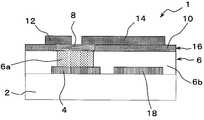
우선, 도 1을 이용하여, 제1 실시 형태의 박막 트랜지스터 (1)의 구성을 설명한다.First, the configuration of the
도 1은, 제1 실시 형태에서의 박막 트랜지스터 (1)의 개략 구성을 도시하는 단면도이다.1 is a cross-sectional view showing a schematic structure of a
도 1 중에 도시된 바와 같이, 박막 트랜지스터 (1)은 절연 기판 (2)와, 게이트 전극 (4)와, 게이트 절연층 (6)과, 반도체 영역 (8)과, 절연 영역 (10)과, 소스 전극 (12)와, 드레인 전극 (14)를 구비하고 있다.1, the
즉, 제1 실시 형태의 박막 트랜지스터 (1)은 바텀 게이트-톱 콘택트형의 박막 트랜지스터 (1)이다.That is, the
(절연 기판 (2)의 상세한 구성)(Detailed configuration of the insulating substrate 2)
이하, 도 1을 참조하여, 절연 기판 (2)의 상세한 구성에 대해서 설명한다.Hereinafter, the detailed configuration of the insulating
절연 기판 (2)의 재료로서는, 예를 들면, 유리나 플라스틱 기판을 이용하는 것이 가능하다.As the material of the insulating
제1 실시 형태에서는, 절연 기판 (2)의 재료로서 플라스틱 기판을 이용하여, 절연 기판 (2)를 수지 기판으로 한다.In the first embodiment, a plastic substrate is used as the material of the insulating
여기서, 플라스틱 기판으로서는, 예를 들면, 폴리메틸메타크릴레이트, 폴리아크릴레이트, 폴리카보네이트, 폴리스티렌, 폴리에틸렌술피드, 폴리에테르술폰(PES), 폴리올레핀, 폴리에틸렌테레프탈레이트, 폴리에틸렌나프탈레이트(PEN), 시클로올레핀 중합체, 폴리에테르살펜, 트리아세틸셀룰로오스, 폴리비닐플루오라이드 필름, 에틸렌-테트라플루오로에틸렌 공중합 수지, 내후성 폴리에틸렌테레프탈레이트, 내후성 폴리프로필렌, 유리 섬유 강화 아크릴 수지 필름, 유리 섬유 강화 폴리카보네이트, 투명성 폴리이미드, 불소계 수지, 환상 폴리올레핀계 수지 등을 이용하는 것이 가능하다.As the plastic substrate, for example, there may be used a plastic substrate such as polymethyl methacrylate, polyacrylate, polycarbonate, polystyrene, polyethylene sulfide, polyethersulfone (PES), polyolefin, polyethylene terephthalate, polyethylene naphthalate A weather-resistant polypropylene, a glass fiber-reinforced acrylic resin film, a glass fiber-reinforced polycarbonate, a transparent polyolefin resin, a polyolefin resin, a polyolefin resin, A fluorine-based resin, a cyclic polyolefin-based resin, or the like can be used.
이들 기판은, 단독으로 이용하는 것도 가능하지만, 2종 이상을 적층한 복합 기판을 이용하는 것도 가능하다. 또한, 유리나 플라스틱 기판 상에, 수지층, 예를 들면, 컬러 필터가 형성된 기판을 적층하는 것도 가능하다.These substrates may be used alone or in combination of two or more. It is also possible to laminate a resin layer, for example, a substrate on which a color filter is formed, on a glass or plastic substrate.
(게이트 전극 (4)의 상세한 구성)(Detailed configuration of the gate electrode 4)
이하, 도 1을 참조하여, 게이트 전극 (4)의 상세한 구성에 대해서 설명한다.Hereinafter, the detailed structure of the
게이트 전극 (4)는 절연 기판 (2) 상의 일부를 덮도록 형성되어 있다.The
게이트 전극 (4)의 재료로서는, 예를 들면, 산화인듐(In2O3), 산화주석(SnO2), 산화아연(ZnO), 산화카드뮴(CdO), 산화인듐카드뮴(CdIn2O4), 산화카드뮴주석(Cd2SnO4), 산화아연주석(Zn2SnO4), 산화인듐아연(In-Zn-O) 등의 산화물 재료를 이용하는 것이 바람직하다.Examples of the material of the
또한, 게이트 전극 (4)의 재료로서는, 예를 들면, 상기한 산화물 재료에 불순물을 도핑한 재료를 이용하는 것도, 도전율을 높이기 위해서 바람직하다. 이 경우, 예를 들면, 산화인듐에 주석이나 몰리브덴, 티탄을 도핑한 것, 산화주석에 안티몬이나 불소를 도핑한 것, 산화아연에 인듐, 알루미늄, 갈륨을 도핑한 것 등을 이용하는 것이 가능하다. 이 중에서는, 특히, 산화인듐에 주석을 도핑한 산화인듐주석(통칭 ITO)이 낮은 저항률 때문에, 특히 바람직하다.As the material of the
또한, 게이트 전극 (4)의 재료로서는, 예를 들면, Au, Ag, Cu, Cr, Al, Mg, Li 등의 저저항 금속 재료를 이용하는 것도 바람직하다.It is also preferable to use a low resistance metal material such as Au, Ag, Cu, Cr, Al, Mg, or Li as the material of the
또한, 게이트 전극 (4)의 재료로서는, 예를 들면, 도전성 산화물 재료와 저저항 금속 재료를 복수 적층한 것을 이용하는 것도 가능하다. 이 경우, 금속 재료의 산화나 경시 열화를 막기 위해서, 도전성 산화물 박막, 금속 박막, 도전성 산화물 박막의 순서로 적층한 3층 구조가 특히 바람직하다.As the material of the
또한, 게이트 전극 (4)의 재료로서는, 예를 들면, PEDOT(폴리에틸렌디옥시티오펜) 등의 유기 도전성 재료를 이용하는 것도 바람직하다.As the material of the
(게이트 절연층 (6)의 상세한 구성)(Detailed configuration of the gate insulating layer 6)
이하, 도 1을 참조하여, 게이트 절연층 (6)의 상세한 구성에 대해서 설명한다.Hereinafter, the detailed structure of the
게이트 절연층 (6)은 절연 기판 (2) 및 게이트 전극 (4) 상에 형성되어, 게이트 전극 (4)를 덮도록 설치되어 있고, 제1 게이트 절연층 (6a)와, 제2 게이트 절연층 (6b)를 갖고 있다.The
또한, 게이트 절연층 (6)의 두께(막 두께)는 예를 들면, 50 nm 이상 2 ㎛ 이하의 범위 내로 하는 것이 바람직하다.The thickness (film thickness) of the
제1 게이트 절연층 (6a)는 절연 기판 (2) 및 게이트 전극 (4) 상에서, 게이트 전극 (4)의 일부를 덮도록 형성되어 있고, 반도체 영역 (8)에 접하는 위치에 형성되어 있다.The first
제1 게이트 절연층 (6a)의 재료로서는, 예를 들면, CVD법에 의해 형성된 질화실리콘을 이용한다. 이 경우, CVD법에 의해 형성된 질화실리콘의 출발 원료로서는, SiH4/NH3 등을 들 수 있다. 또한, 제1 게이트 절연층 (6a)의 재료는 CVD법에 의해 형성된 질화실리콘에 한정하는 것은 아니다.As the material of the first
제1 게이트 절연층 (6a) 중의 수소 원자의 농도는 1×10²⁰/cm3 이상 5×10²²/cm3 이하의 범위 내이다.The concentration of hydrogen atoms in the first
제1 게이트 절연층 (6a) 중의 수소 원자의 농도를, 1×10²⁰/cm3 이상 5×10²²/cm3 이하의 범위 내로 하는 이유는, 제1 게이트 절연층 (6a) 상에 형성된 반도체 영역 (8)의 도전율을 높게 하는 것이 가능해지기 때문이다.The reason why the concentration of hydrogen atoms in the first
이것은, 수소를 많이 포함하는 게이트 절연층 (6)은 그 위에 형성된 금속 산화물층인 반도체 영역 (8)에 게이트 절연층 (6)으로부터 수소가 확산하기 쉬워지기 때문에, 확산한 수소가 금속 산화물 중에서 p형 도펀트로서 기능하여, 금속 산화물층인 반도체 영역 (8)의 도전율이 증가하기 때문이다.This is because hydrogen easily diffuses from the
따라서, 제1 게이트 절연층 (6a) 중의 수소 원자의 농도는 1×10²⁰/cm3 미만이면, 금속 산화물 중에 확산하는 수소의 양이 적기 때문에, 금속 산화물의 도전성이 증가하지 않아, 제1 게이트 절연층 (6a) 상에 형성된 반도체 영역 (8)을 반도체층으로 할 수 없게 된다.Therefore, if the concentration of hydrogen atoms in the first
또한, 제1 실시 형태에서는, 후술하는 바와 같이, 제1 게이트 절연층 (6a)를 CVD법을 이용하여 형성한 재료에 의해 형성한다. 이 때문에, 제1 게이트 절연층 (6a) 중의 수소 원자는, 원료 가스로서 일반적으로 이용되는 NH3 가스에서 유래하는 것이 된다.In the first embodiment, as described later, the first
이 때문에, 제1 게이트 절연층 (6a) 중의 수소 원자의 농도가 5×10²²/cm3보다 커지도록 형성하면, 원료 가스 농도에 있어서의 NH3 가스 농도가 너무 높기 때문에, SiN막을 형성할 수 없어, 게이트 절연층 (6)을 CVD법에 의해 성막할 수 없게 된다.Therefore, if the concentration of the hydrogen atoms in the first
또한, 제1 게이트 절연층 (6a)의 저항율은, 1011 Ω·cm 이상이 바람직하고, 보다 적합하게는, 1012 Ω·cm 이상이다. 이것은, 제1 게이트 절연층 (6a)의 저항율이 1011 Ω·cm보다 작으면, 게이트 절연층 (6) 전체로서 충분한 절연성을 발휘할 수 없어, 게이트 누설 전류가 증대하기 때문에, 양호한 소자 특성을 얻을 수 없기 때문이다.The resistivity of the first
제2 게이트 절연층 (6b)는 절연 기판 (2) 및 게이트 전극 (4) 상에서, 절연 기판 (2)와, 게이트 전극 (4)의, 제1 게이트 절연층 (6a)가 덮고 있지 않은 부분을 덮도록 형성되어 있고, 절연 영역 (10)에 접하는 위치에 형성되어 있다.The second
제2 게이트 절연층 (6b)의 재료로서는, 예를 들면, 산화실리콘, 질화실리콘, 실리콘옥시니트라이드, 산화알루미늄을 이용하는 것이 특히 바람직하다.As the material of the second
여기서, 제1 실시 형태에서는, 제2 게이트 절연층 (6b)의 재료로서, CVD법으로 형성한 산화실리콘을 이용한다.Here, in the first embodiment, silicon oxide formed by the CVD method is used as the material of the second
또한, 제1 실시 형태에서는, 제2 게이트 절연층 (6b)를 산화실리콘, 질화실리콘, 실리콘옥시니트라이드, 산화알루미늄 중 어느 하나의 화합물을 포함한 층으로서 형성한다.In the first embodiment, the second
또한, 제2 게이트 절연층 (6b)의 재료로서는, 예를 들면, 산화탄탈, 산화이트륨, 산화하프늄, 하프늄알루미네이트, 산화지르코니아, 산화티탄 등도 이용하는 것도 가능하고, 이들 재료를 이용함으로써, 게이트 누설 전류를 억제하기 위해서 충분한 절연성을 얻을 수 있다.As the material of the second
또한, 제2 게이트 절연층 (6b)의 재료는 상기한 재료에 한정하는 것은 아니다.The material of the second
제2 게이트 절연층 (6b) 중의 수소 원자의 농도는 1×10²⁰/cm3 미만이다.The concentration of hydrogen atoms in the second
제2 게이트 절연층 (6b) 중의 수소 원자의 농도를, 1×10²⁰/cm3 미만으로 하는 이유는, 제2 게이트 절연층 (6b) 상에 형성된 금속 산화물층인 절연 영역 (10)의 도전율을 제1 게이트 절연층 (6a) 상에 형성된 금속 산화물층인 반도체 영역 (8)의 도전율보다도 낮게 하는 것이 가능해지고, 이에 따라, 인접하는 TFT의 금속 산화물을 포함하는 반도체층들을 제2 게이트 절연층 (6b)에 의해 절연하는 것이 가능해지기 때문이다.The reason why the concentration of hydrogen atoms in the second
이 때문에, 제2 게이트 절연층 (6b) 중의 수소 원자의 농도가 1020/cm3 이상이면, 제2 게이트 절연층 (6b) 상의 금속 산화물인 절연 영역 (10)에, 제2 게이트 절연층 (6b) 중의 수소 원자가 확산하여, 제2 게이트 절연층 (6b) 상의 금속 산화물인 절연 영역 (10)의 도전성이 증가하여, 절연층으로서의 기능이 손상되게 된다.Therefore, if the concentration of hydrogen atoms in the second
또한, 제2 게이트 절연층 (6b)의 저항율은, 제1 게이트 절연층 (6a)와 마찬가지로, 1011 Ω·cm 이상이 바람직하고, 보다 적합하게는, 1012 Ω·cm 이상이다. 이것은, 제2 게이트 절연층 (6b)의 저항율이 1011 Ω·cm보다 작으면, 게이트 절연층 (6) 전체로서 충분한 절연성을 발휘할 수 없어, 게이트 누설 전류가 증대하기 때문에, 양호한 소자 특성을 얻을 수 없기 때문이다.The resistivity of the second
(반도체 영역 (8)의 상세한 구성)(Detailed configuration of the semiconductor region 8)
이하, 도 1을 참조하여, 반도체 영역 (8)의 상세한 구성에 대해서 설명한다.Hereinafter, the detailed structure of the
반도체 영역 (8)은 채널을 포함하고 있고, 게이트 절연층 (6) 중, 제1 게이트 절연층 (6a)에 접하는 부분에 형성되어 있다.The
또한, 반도체 영역 (8)은 절연 영역 (10)과 함께, 상기한 금속 산화물층 (16)을 형성하고 있다. 구체적으로는, 반도체 영역 (8)과 절연 영역 (10)은 동시에 성막된 하나의 층인 금속 산화물층 (16)의 막 중에 존재하고 있다.The
반도체 영역 (8)의 재료로서는, 예를 들면, 아연, 인듐, 주석, 텅스텐, 마그네슘, 갈륨 중 1 종류 이상의 원소를 포함하는 산화물을 이용하는 것이 가능하다.As the material of the
여기서, 제1 실시 형태에서는, 반도체 영역 (8)의 재료로서, 인듐, 아연, 갈륨 중, 어느 하나를 포함하는 재료를 이용한다.Here, in the first embodiment, as the material of the
또한, 반도체 영역 (8)의 재료로서는, 예를 들면, 산화아연, 산화인듐, 산화인듐아연, 산화주석, 산화텅스텐, 산화아연갈륨인듐(In-Ga-Zn-O) 등 공지된 재료를 이용하는 것이 가능하다.As the material of the
또한, 반도체 영역 (8)의 재료는 상술한 재료에 한정하는 것은 아니다.The material of the
반도체 영역 (8)의 두께(막 두께)는 적어도 10 nm 이상으로 하는 것이 바람직하다. 이것은, 반도체 영역 (8)의 막 두께가 10 nm 미만이면, 섬 형상 성장에 의해, 반도체 영역 (8) 중에 반도체가 형성되어 있지 않은 부분이 생긴다는 문제가 발생할 수 있기 때문이다.The thickness (film thickness) of the
(절연 영역 (10)의 상세한 구성)(Detailed configuration of the insulating region 10)
이하, 도 1을 참조하여, 절연 영역 (10)의 상세한 구성에 대해서 설명한다.Hereinafter, with reference to Fig. 1, the detailed structure of the insulating
절연 영역 (10)은 게이트 절연층 (6) 중, 제2 게이트 절연층 (6b)에 접하는 부분에 형성되어 있다.The insulating
절연 영역 (10)의 재료로서는, 상술한 반도체 영역 (8)과 동일하게, 예를 들면, 아연, 인듐, 주석, 텅스텐, 마그네슘, 갈륨 중 1 종류 이상의 원소를 포함하는 산화물을 이용하는 것이 가능하다.As the material of the insulating
여기서, 제1 실시 형태에서는, 절연 영역 (10)의 재료로서, 인듐, 아연, 갈륨 중, 어느 하나를 포함하는 재료를 이용한다.Here, in the first embodiment, a material containing any one of indium, zinc, and gallium is used as the material of the insulating
또한, 절연 영역 (10)의 재료로서는, 상술한 반도체 영역 (8)과 같이 예를 들면, 산화아연, 산화인듐, 산화인듐아연, 산화주석, 산화텅스텐, 산화아연갈륨인듐(In-Ga-Zn-O) 등 공지된 재료를 이용하는 것이 가능하다.As the material of the insulating
또한, 절연 영역 (10)의 재료는 상술한 재료에 한정하는 것은 아니다.Further, the material of the insulating
절연 영역 (10)의 두께(막 두께)는 상술한 반도체 영역 (8)과 동일하게, 적어도, 10 nm 이상으로 하는 것이 바람직하다. 이것은, 절연 영역 (10)의 막 두께가 10 nm 미만이면, 상술한 반도체 영역 (8)과 같이 섬 형상 성장에 의해, 절연 영역 (10) 중에 반도체가 형성되어 있지 않은 부분이 생긴다는 문제가 발생할 수 있기 때문이다. 또한, 절연 영역 (10)의 도전율은 10-9 S/cm 미만인 것이 바람직하다. 그 이유는, 절연 영역 (10)의 도전율이 10-9 S/cm 이상이면, 절연 영역 (10)으로서의 기능이 발휘되지 않아, 반도체 영역 (8)로부터 누설 전류가 흐를 우려가 있기 때문이다.The thickness (film thickness) of the insulating
(소스 전극 (12)의 상세한 구성)(Detailed configuration of the source electrode 12)
이하, 도 1을 참조하여, 소스 전극 (12)의 상세한 구성에 대해서 설명한다.Hereinafter, the detailed configuration of the
소스 전극 (12)는 금속 산화물층 (16) 상의 일부를 덮도록 형성되어 있다.The
소스 전극 (12)의 재료로서는, 상술한 게이트 전극 (4)와 동일하게, 예를 들면, 산화인듐(In2O3), 산화주석(SnO2), 산화아연(ZnO), 산화카드뮴(CdO), 산화인듐카드뮴(CdIn2O4), 산화카드뮴주석(Cd2SnO4), 산화아연주석(Zn2SnO4), 산화인듐아연(In-Zn-O) 등의 산화물 재료를 이용하는 것이 바람직하다.As the material of the
또한, 소스 전극 (12)의 재료로서는, 상술한 게이트 전극 (4)와 동일하게, 예를 들면, 상기한 산화물 재료에 불순물을 도핑한 재료를 이용하는 것도, 도전율을 높이기 위해서 바람직하다. 이 경우, 예를 들면, 산화인듐에 주석이나 몰리브덴, 티탄을 도핑한 것, 산화주석에 안티몬이나 불소를 도핑한 것, 산화아연에 인듐, 알루미늄, 갈륨을 도핑한 것 등을 이용하는 것이 가능하다. 이 중에서는, 특히, 산화인듐에 주석을 도핑한 산화인듐주석(통칭 ITO)이 낮은 저항률 때문에 특히 바람직하다.As the material of the
또한, 소스 전극 (12)의 재료로서는, 상술한 게이트 전극 (4)와 동일하게, 예를 들면, Au, Ag, Cu, Cr, Al, Mg, Li 등의 저저항 금속 재료를 이용하는 것도 바람직하다.It is also preferable to use a low resistance metal material such as Au, Ag, Cu, Cr, Al, Mg, or Li as the material of the
또한, 소스 전극 (12)의 재료로서는, 상술한 게이트 전극 (4)와 동일하게, 예를 들면, 도전성 산화물 재료와 저저항 금속 재료를 복수 적층한 것을 이용하는 것도 가능하다. 이 경우, 금속 재료의 산화나 경시 열화를 막기 위해서, 도전성 산화물 박막, 금속 박막, 도전성 산화물 박막의 순서로 적층한 3층 구조가 특히 바람직하다.As the material of the
또한, 소스 전극 (12)의 재료로서는, 상술한 게이트 전극 (4)와 동일하게, 예를 들면, PEDOT(폴리에틸렌디옥시티오펜) 등의 유기 도전성 재료를 이용하는 것도 바람직하다.As the material of the
(드레인 전극 (14)의 상세한 구성)(Detailed configuration of the drain electrode 14)
이하, 도 1을 참조하여, 드레인 전극 (14)의 상세한 구성에 대해서 설명한다.Hereinafter, the detailed structure of the
드레인 전극 (14)는 금속 산화물층 (16) 상에서, 소스 전극 (12)가 덮고 있지 않은 부분의 적어도 일부를 덮도록 형성되어 있다.The
드레인 전극 (14)의 재료로서는, 상술한 게이트 전극 (4)와 동일하게, 예를 들면, 산화인듐(In2O3), 산화주석(SnO2), 산화아연(ZnO), 산화카드뮴(CdO), 산화인듐카드뮴(CdIn2O4), 산화카드뮴주석(Cd2SnO4), 산화아연주석(Zn2SnO4), 산화인듐아연(In-Zn-O) 등의 산화물 재료를 이용하는 것이 바람직하다.As the material of the
또한, 드레인 전극 (14)의 재료로서는, 상술한 게이트 전극 (4)와 동일하게, 예를 들면, 상기한 산화물 재료에 불순물을 도핑한 재료를 이용하는 것도, 도전율을 높이기 위해서 바람직하다. 이 경우, 예를 들면, 산화인듐에 주석이나 몰리브덴, 티탄을 도핑한 것, 산화주석에 안티몬이나 불소를 도핑한 것, 산화아연에 인듐, 알루미늄, 갈륨을 도핑한 것 등을 이용하는 것이 가능하다. 이 중에서는, 특히, 산화인듐에 주석을 도핑한 산화인듐주석(ITO)이 낮은 저항률 때문에 특히 바람직하다.Also, as the material of the
또한, 드레인 전극 (14)의 재료로서는, 상술한 게이트 전극 (4)와 동일하게, 예를 들면, Au, Ag, Cu, Cr, Al, Mg, Li 등의 저저항 금속 재료를 이용하는 것도 바람직하다.It is also preferable to use a low resistance metal material such as Au, Ag, Cu, Cr, Al, Mg, or Li as the material of the
또한, 드레인 전극 (14)의 재료로서는, 상술한 게이트 전극 (4)와 동일하게, 예를 들면, 도전성 산화물 재료와 저저항 금속 재료를 복수 적층한 것을 이용하는 것도 가능하다. 이 경우, 금속 재료의 산화나 경시 열화를 막기 위해서, 도전성 산화물 박막, 금속 박막, 도전성 산화물 박막의 순서로 적층한 3층 구조가 특히 바람직하다.As the material of the
또한, 드레인 전극 (14)의 재료로서는, 상술한 게이트 전극 (4)와 동일하게, 예를 들면, PEDOT(폴리에틸렌디옥시티오펜) 등의 유기 도전성 재료를 이용하는 것도 바람직하다.As the material of the
또한, 게이트 전극 (4)의 재료와, 소스 전극 (12)의 재료와, 드레인 전극 (14)의 재료는, 전부 동일 재료를 이용할 수도 있고, 또한 전부 다른 재료를 이용할 수도 있다. 그러나, 박막 트랜지스터 (1)의 제조에 있어서, 그의 제조 공정수를 저감하기 위해서는, 소스 전극 (12)의 재료와 드레인 전극 (14)의 재료는 동일한 재료인 것이 보다 바람직하다.The material of the
(화상 표시 장치)(Image display device)
다음으로, 도 1을 참조하여, 상술한 박막 트랜지스터 (1)을 구비하는 화상 표시 장치의 구성에 대해서 설명한다.Next, with reference to Fig. 1, the structure of the image display apparatus having the above-described
화상 표시 장치(도시하지 않음)는 예를 들면, 컬러 디스플레이이고, 박막 트랜지스터 (1)을 구비하는 박막 트랜지스터 어레이(도시하지 않음)와, 화상 표시 매체(도시하지 않음)를 구비하고 있다.An image display device (not shown) is, for example, a color display, and includes a thin film transistor array (not shown) having a
또한, 화상 표시 장치에 구비된 화상 표시 매체는 전기 영동 방식의 표시 매체이다.The image display medium provided in the image display apparatus is an electrophoretic display medium.
또한, 화상 표시 장치에 구비된 박막 트랜지스터 (1)로서는, 후술하는 박막 트랜지스터 (1)의 제조 방법에 의해 제조한 것을 이용할 수도 있다.As the
(박막 트랜지스터 (1)의 제조 방법)(Manufacturing method of thin film transistor 1)
이하, 도 1을 참조하여, 박막 트랜지스터 (1)의 제조 방법을 설명한다.Hereinafter, a method of manufacturing the
박막 트랜지스터 (1)을 제조하는 때에는, 우선, 절연 기판 (2) 상에 게이트 전극 (4)를 형성하는 게이트 전극 형성 공정을 행한다. 즉, 박막 트랜지스터 (1)의 제조 방법에는 게이트 전극 형성 공정을 포함한다.In manufacturing the
게이트 전극 형성 공정에서, 게이트 전극 (4)를 형성하는 방법으로서는, 예를 들면, 진공 증착법, 이온 플레이팅법, 스퍼터링법, 레이저 어블레이션법, 플라즈마 CVD(Chemical Vapor Deposition), 광 CVD, 핫와이어 CVD법 등을 이용하는 것이 가능하다.Examples of the method for forming the
또한, 게이트 전극 (4)를 형성하는 방법으로서는, 예를 들면, 상술한 도전성 재료를, 잉크상이나, 페이스트상으로 한 것을, 스크린 인쇄, 철판 인쇄, 요판 인쇄, 반전 오프셋 인쇄, 잉크젯트법 등으로 도포하고, 소성하여 형성하는 방법을 이용하는 것이 가능하다.As a method of forming the
또한, 게이트 전극 (4)를 형성하는 방법은 상술한 방법에 한정하는 것은 아니다.The method of forming the
그리고, 절연 기판 (2) 상에 게이트 전극 (4)를 형성한 후, 절연 기판 (2) 및 게이트 전극 (4) 상에 게이트 절연층 (6)을 형성하는 게이트 절연층 형성 공정을 행한다. 즉, 박막 트랜지스터 (1)의 제조 방법은 게이트 절연층 형성 공정을 포함한다.After the
게이트 절연층 형성 공정에서, 제1 게이트 절연층 (6a)를 형성하는 방법으로서는 CVD법을 이용한다.In the step of forming the gate insulating layer, a CVD method is used as a method of forming the first
또한, 게이트 절연층 형성 공정에서, 제2 게이트 절연층 (6b)를 형성하는 방법으로서는, 예를 들면, 스퍼터링법, 플라즈마 CVD법, 또는 원자층 퇴적법을 이용하는 것이 바람직하는데, 진공 증착법, 이온 플레이팅법, 레이저 어블레이션법 등의 방법을 이용할 수도 있다.The second
또한, 제2 게이트 절연층 (6b)를 형성하는 때에는, 막의 성장 방향으로 향하여 조성의 구배를 실행할 수도 있다.In forming the second
게이트 절연층 형성 공정에 의해, 절연 기판 (2) 및 게이트 전극 (4) 상에 게이트 절연층 (6)을 형성한 후, 게이트 절연층 (6) 상에 금속 산화물층 (16)을 형성하는 금속 산화물층 형성 공정을 행한다. 즉, 박막 트랜지스터 (1)의 제조 방법은 금속 산화물층 형성 공정을 포함한다.The
금속 산화물층 형성 공정에서는, 반도체 영역 (8)을 형성하는 반도체 영역 형성 공정과, 절연 영역 (10)을 형성하는 절연 영역 형성 공정을 포함한다.In the metal oxide layer forming step, a semiconductor region forming step for forming the
여기서, 제1 실시 형태의 금속 산화물층 형성 공정에서는, 반도체 영역 형성 공정과 절연 영역 형성 공정을 동시에 행한다. 즉, 제1 실시 형태의 박막 트랜지스터 (1)의 제조 방법에서는, 반도체 영역 (8)과 절연 영역 (10)을 동시에 성막한다.Here, in the metal oxide layer forming step of the first embodiment, the semiconductor region forming step and the insulating region forming step are performed at the same time. That is, in the method of manufacturing the
금속 산화물층 형성 공정에서, 반도체 영역 (8)과 절연 영역 (10)을 형성하는 방법으로서는, 예를 들면, 스퍼터링법, 펄스 레이저 퇴적법, 진공 증착법, CVD법, 졸겔법 등의 방법을 이용한다.As the method for forming the
금속 산화물층 형성 공정에서, 반도체 영역 (8)과 절연 영역 (10)을 형성하는 방법으로서, 보다 적합하게는, 스퍼터링법, 펄스 레이저 퇴적법, 진공 증착법, CVD법을 이용한다.More preferably, a sputtering method, a pulse laser deposition method, a vacuum deposition method, or a CVD method is used as a method for forming the
이 경우, 스퍼터링법으로서는, RF 마그네트론 스퍼터링법, DC 스퍼터링법, 이온빔 스퍼터링법을 이용한다. 또한, 진공 증착법으로서는, 가열 증착, 전자빔 증착, 이온 플레이팅법을 이용한다. 또한, CVD법으로서는, 핫와이어 CVD법, 플라즈마 CVD법 등을 이용한다.In this case, as the sputtering method, RF magnetron sputtering, DC sputtering, and ion beam sputtering are used. As the vacuum deposition method, a heating deposition, an electron beam deposition, and an ion plating method are used. As the CVD method, a hot wire CVD method, a plasma CVD method, or the like is used.
또한, 반도체 영역 (8) 및 절연 영역 (10)을 형성하는 방법은 상술한 방법에 한정하는 것은 아니다.The method of forming the
또한, 금속 산화물층 형성 공정에서, 반도체 영역 (8)을 형성하는 때에는, 반도체 영역 (8)의 도전율이 10-7 S/cm 이상 10-3 S/cm 이하의 범위 내가 되도록 성막한다.In forming the
이 때, 특히 패터닝 등은 하지 않고서, 반도체 영역 (8)을 게이트 절연층 (6) 상에 균일하게 성막하는 것만으로, 제1 게이트 절연층 (6a)으로부터의 수소 원자의 확산에 의해, 제1 게이트 절연층 (6a) 상에 위치하는 반도체 영역 (8)이 반도체층이 된다.At this time, only by uniformly depositing the
한편, 금속 산화물층 형성 공정에서, 절연 영역 (10)을 형성하는 때에는, 절연 영역 (10)의 도전율이 10-7 S/cm 미만이 되도록 성막한다.On the other hand, in forming the
이 때, 제2 게이트 절연층 (6b) 상에 위치하는 절연 영역 (10)은 도전율이 10-7 S/cm 미만의 절연층으로 남아있기 때문에, 특히 반도체층의 패터닝 공정을 설치하는 일 없이, 인접하는 TFT의 반도체층들을 절연하는 것이 가능해져, 반도체층의 패터닝 공정을 생략하는 것이 가능해진다.At this time, since the insulating
또한, 상술한 바와 같이, 반도체 영역 (8)의 도전율을 10-7 S/cm 이상 10-3 S/cm 이하의 범위 내로 하고, 절연 영역 (10)의 도전율을 10-7 S/cm 미만으로 하도록 게이트 절연층 (6) 및 금속 산화물층 (16)을 성막함으로써 높은 신뢰성을 갖는 박막 트랜지스터 (1)을 얻는 것이 가능해지고, 또한 반도체층의 패터닝 공정이 필요없기 때문에, 생산성이 우수한 박막 트랜지스터 (1)의 제조 방법을 얻는 것이 가능해진다.As described above, when the conductivity of the
금속 산화물층 형성 공정에 의해, 게이트 절연층 (6) 상에 금속 산화물층 (16)을 형성한 후, 금속 산화물층 (16) 상에, 소스 전극 (12)와 드레인 전극 (14)를 형성하는 소스 전극 형성 공정 및 드레인 전극 형성 공정을 행한다. 즉, 박막 트랜지스터 (1)의 제조 방법은 소스 전극 형성 공정 및 드레인 전극 형성 공정을 포함한다.The
소스 전극 형성 공정 및 드레인 전극 형성 공정에서, 소스 전극 (12)와 드레인 전극 (14)를 형성하는 방법으로서는, 상술한 게이트 전극 형성 공정에서 게이트 전극 (4)를 형성하는 방법과 동일하게, 예를 들면, 진공 증착법, 이온 플레이팅법, 스퍼터링법, 레이저 어블레이션법, 플라즈마 CVD, 광 CVD, 핫와이어 CVD법 등을 이용하는 것이 가능하다.As the method of forming the
또한, 소스 전극 (12)와 드레인 전극 (14)를 형성하는 방법으로서는, 예를 들면, 상술한 도전성 재료를, 잉크상이나, 페이스트상으로 한 것을, 스크린 인쇄, 철판 인쇄, 요판 인쇄, 반전 오프셋 인쇄, 잉크젯트법 등으로 도포하고, 소성하여 형성하는 방법을 이용하는 것이 가능하다.Examples of the method for forming the
또한, 소스 전극 (12)와 드레인 전극 (14)를 형성하는 방법은 상술한 방법에 한정하는 것은 아니다.The method of forming the
소스 전극 (12)와 드레인 전극 (14)가 형성되면, 박막 트랜지스터 (1)의 제조를 종료한다.When the
금속 산화물의 반도체 영역 상에는 필요에 따라서 절연성의 밀봉층을 형성하는 것이 바람직하다. 밀봉층을 구성하는 무기 재료로서는, 산화실리콘, 질화실리콘, 실리콘옥시니트라이드, 산화알루미늄이 특히 바람직하다. 또한 산화탄탈, 산화이트륨, 산화하프늄, 하프늄알루미네이트, 산화지르코니아, 산화티탄 등도 들 수 있어, 이들 재료를 이용함으로써 밀봉층으로서 충분한 기능을 발휘할 수 있다. 이들 무기 재료는 스퍼터링법, 플라즈마 CVD법 또는 원자 퇴적법에 의해 형성할 수 있다. 그러나, 진공 증착법, 이온 플레이팅법, 레이저 어블레이션법 등의 방법을 이용하더라도 상관없다.It is preferable to form an insulating sealing layer on the semiconductor region of the metal oxide if necessary. As the inorganic material constituting the sealing layer, silicon oxide, silicon nitride, silicon oxynitride and aluminum oxide are particularly preferable. In addition, tantalum oxide, yttrium oxide, hafnium oxide, hafnium aluminate, zirconia oxide, titanium oxide, and the like can be used. By using these materials, sufficient function as a sealing layer can be exhibited. These inorganic materials can be formed by a sputtering method, a plasma CVD method, or an atomic deposition method. However, a vacuum evaporation method, an ion plating method, a laser ablation method, or the like may be used.
또한, 밀봉층을 구성하는 유기 재료로서는, 불소 수지나, 불소를 측쇄에 갖는 실리콘 수지 등의, 고분자 수지의 수소를 불소로 대체한 불소화 수지를 이용할 수도 있다. 구체적으로는, 불소화에폭시, 불소화아크릴, 불소화폴리이미드, 폴리불화비닐리덴, 불소화올레핀·프로필렌 공중합체, 불소화올레핀·비닐에테르 공중합체, 불소화올레핀·비닐에스테르 공중합체, 불소화에테르환화 중합체 등을 사용할 수 있다. 또한, 불소화 수지에는, 일부의 수소를 불소로 대체한 부분 불소화 수지와, 모든 수소를 불소로 대체한 전체 불소화 수지가 있는데, 전체 불소화 수지쪽이 보다 바람직하다. 통상의 비불소화 수지(에폭시나 아크릴 등)와 달리, 불소화 수지는 안정성이 우수한 물질로서, 반도체층에 영향을 미치지 않는다. 무기 절연막의 경우, 패터닝에는 리프트오프법이 바람직하다.As the organic material constituting the sealing layer, a fluorinated resin obtained by replacing hydrogen of a polymer resin with fluorine, such as a fluororesin or a silicone resin having fluorine on the side chain, may be used. Specifically, fluorinated epoxies, fluorinated acrylics, fluorinated polyimides, polyvinylidene fluoride, fluorinated olefin-propylene copolymers, fluorinated olefin-vinyl ether copolymers, fluorinated olefin-vinyl ester copolymers, and fluorinated ether cyclization polymers can be used have. The fluorinated resin includes a partially fluorinated resin in which a part of hydrogen is replaced by fluorine and a whole fluorinated resin in which all hydrogen is replaced by fluorine, and the whole fluorinated resin is more preferable. Unlike ordinary non-fluorinated resins (such as epoxy or acrylic), fluorinated resins are excellent in stability and do not affect the semiconductor layer. In the case of the inorganic insulating film, the lift-off method is preferable for patterning.
불소화 수지의 경우, 패터닝은 인쇄(스크린 인쇄, 플렉소 인쇄, 반전 인쇄, 잉크젯 인쇄 등)으로 행할 수 있지만, 스핀 코팅이나 다이 코팅에 의해서 전체면에 형성 후, 컨택트부만을 핀셋 등으로 박리할 수도 있다.In the case of a fluorinated resin, patterning can be performed by printing (screen printing, flexographic printing, reversal printing, inkjet printing, etc.), but after forming on the entire surface by spin coating or die coating, have.
(상기 박막 트랜지스터 (1)을 이용한 화상 표시 장치)(An image display apparatus using the thin film transistor 1)
제1 실시 형태의 화상 표시 장치는, 도 3이나 도 4에 일례를 도시한 바와 같이, 상기 구성의 박막 트랜지스터 상에, 적어도 층간 절연층 (22), 화소 전극 (24), 전기 영동체 (32), 및 대향 전극 (30)이 배치되어 구성되어 있다.3 and 4, the image display apparatus of the first embodiment includes at least an interlayer insulating
층간 절연층 (22)는 진공 증착법, 이온 플레이팅법, 스퍼터링법, 레이저 어블레이션법, 플라즈마 CVD, 광 CVD, 핫와이어 CVD법 등의 드라이 제막이나, 스핀 코팅법, 침지 코팅법, 스크린 인쇄법 등의 웨트 성막법을 재료에 따라서 적절하게 사용하여 형성된다. 층간 절연층 (22)는 드레인 전극 (14) 상에 개구부를 갖고 있고, 이 개구부를 통해 드레인 전극 (14)와 화소 전극 (24)를 접속시킬 수 있다. 개구부는 층간 절연층 (180)의 형성과 동시 또는 형성 후에 포토리소그래피법이나 에칭 등의 공지된 방법을 이용하여 설치할 수 있다.The interlayer insulating
그 층간 절연층 (22) 상에 도전성 재료를 성막하고, 소정의 화소 형상으로 패터닝하여 화소 전극 (24)를 형성한다. 드레인 전극 (14)가 노출되도록 개구부가 형성되어 있는 상기 층간 절연층 (22) 상에 화소 전극 (24)를 형성함으로써 드레인 전극 (14)와 화소 전극 (24)의 도통을 취할 수 있다.A conductive material is formed on the
또한, 상기 화소 전극 (24) 상에, 전기 영동체 (32)를 개재하여 대향 전극 (30)을 설치한다. 전기 영동체 (32)는 전기 영동 방식을 이용한 화상 표시 매체이다.Further, the
각 전극 및 절연성 보호층의 패터닝 방법으로서는, 공지 일반의 방법을 사용할 수 있다. 예를 들면, 포토리소그래피법을 이용하여 패턴 형성 부분을 레지스트 등에 의해 보호하고, 에칭에 의해서 불필요 부분을 제거하여 행할 수 있지만, 이 방법에 한정되지 않다.As a method of patterning each of the electrodes and the insulating protective layer, a known general method can be used. For example, the pattern forming portion is protected by a resist or the like using a photolithography method, and the unnecessary portion is removed by etching. However, the present invention is not limited to this method.
(제1 실시 형태의 효과)(Effects of First Embodiment)
이하, 제1 실시 형태의 효과를 열거한다.Hereinafter, the effects of the first embodiment will be listed.
제1 실시 형태의 박막 트랜지스터 (1) 및 박막 트랜지스터 (1)의 제조 방법이면, 금속 산화물층 (16)의 패터닝 공정, 특히, 습식 에칭 공정을 생략하는 것이 가능해지기 때문에, 박막 트랜지스터 (1)의 제조 공정을 간략화하는 것이 가능해진다.The method of manufacturing the
이에 따라, 고품질 또한 저비용으로 제조가 가능한 박막 트랜지스터 (1) 및 그의 제조 방법과, 박막 트랜지스터 (1)을 구비하는 화상 표시 장치를 제공하는 것이 가능해진다.As a result, it is possible to provide the
<제2 실시 형태>≪ Second Embodiment >
다음으로, 본 발명의 제2 실시 형태(이하, 「제2 실시 형태」라고 기재함)에 대해서, 도면을 참조하면서, 제2 실시 형태에 따른 박막 트랜지스터의 구성과, 박막 트랜지스터를 구비하는 화상 표시 장치의 구성과, 박막 트랜지스터의 제조 방법을 설명한다.Next, a second embodiment of the present invention (hereinafter referred to as " second embodiment ") will be described with reference to the drawings, in which the structure of the thin film transistor according to the second embodiment and the image display The configuration of the device and the method of manufacturing the thin film transistor will be described.
(구성)(Configuration)
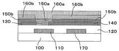
도 6에 본 발명의 실시 형태를 설명하는 박막 트랜지스터의 일례를 도시한다.6 shows an example of a thin film transistor for explaining an embodiment of the present invention.
제2 실시 형태의 박막 트랜지스터는, 도 6에 도시한 바와 같이, 절연 기판 (100) 상에 게이트 전극 (110), 게이트 절연층 (120), 소스 전극 (130), 드레인 전극 (140), 금속 산화물층 (150), 절연성 보호층 (160)을 순서로 적층하여 형성된 바텀 게이트 바텀 컨택트형의 박막 트랜지스터이다. 그리고, 상기 절연성 보호층 (160)은 제1 절연성 보호층 (160a)와 제2 절연성 보호층 (160b)를 포함하고, 상기 금속 산화물층 (150)은 제1 절연성 보호층 (160a) 하에 형성되는 반도체 영역 (150a)와 제2 절연성 보호층 (160b) 하에 형성되는 절연체 영역 (150b)를 포함한다. 채널을 포함하는 반도체 영역 (150a)에 접하는 제1 절연성 보호층 (160a)는 CVD법에 의해 형성된 질화실리콘으로 구성된다.6, the thin film transistor of the second embodiment includes a
제2 실시 형태의 절연 기판으로서, 유리나 플라스틱 기판을 사용할 수 있다. 플라스틱 기판의 구체예로서, 폴리메틸렌메타크릴레이트, 폴리아크릴레이트, 폴리카보네이트, 폴리스티렌, 폴리에틸렌술피드, 폴리에테르술폰, 폴리올레핀, 폴리에틸렌테레프탈레이트, 폴리에틸렌나프탈레이트, 시클로올레핀 중합체, 폴리에테르설폰, 트리아세틸셀룰로오스, 폴리비닐플루오라이드 필름, 에틸렌-테트라플루오로에틸렌, 공중합 수지, 내후성 폴리에틸렌테레프탈레이트, 내후성 폴리프로필렌, 유리 섬유 강화 아크릴 수지 필름, 유리 섬유 강화 폴리카보네이트, 투명성 폴리이미드, 불소계 수지, 환상 폴리올레핀 수지 등을 예시할 수 있다. 단, 본 발명은 이들 재료에 한정되는 것은 아니다. 이들은 단독으로나, 2종 이상이 적층된 복합 기판으로서도 사용할 수 있다. 또한 유리나 플라스틱 기판 상에 컬러 필터와 같은 수지층을 갖는 기판도 사용할 수 있다.As the insulating substrate of the second embodiment, glass or a plastic substrate can be used. As specific examples of the plastic substrate, there may be mentioned polyolefin such as polymethylene methacrylate, polyacrylate, polycarbonate, polystyrene, polyethylene sulfide, polyethersulfone, polyolefin, polyethylene terephthalate, polyethylene naphthalate, cycloolefin polymer, polyethersulfone, triacetyl A film made of glass fiber reinforced acrylic resin, a glass fiber-reinforced polycarbonate, a transparent polyimide, a fluorine resin, a cyclic polyolefin resin, a polyolefin resin such as a polyethylene terephthalate, a weather resistant polypropylene, a glass fiber reinforced acrylic resin film, And the like. However, the present invention is not limited to these materials. These may be used alone or as a composite substrate in which two or more kinds of substrates are laminated. A substrate having a resin layer such as a color filter on a glass or plastic substrate may also be used.
제2 실시 형태의 게이트 전극 (110), 소스 전극 (130), 드레인 전극 (140)에는, 산화인듐(In2O3), 산화주석(SnO2), 산화아연(ZnO), 산화카드뮴(CdO), 산화인듐카드뮴(CdIn2O4), 산화카드뮴주석(Cd2SnO4), 산화아연주석(Zn2SnO4), 산화인듐아연(In-Zn-O) 등의 산화물 재료가 바람직하게 이용된다. 또한 이 산화물 재료에 불순물을 도핑한 것도 바람직하다. 일례로서 산화인듐에 몰리브덴이나 티탄을 도핑한 것, 산화주석에 안티몬이나 불소를 도핑한 것, 산화아연에 인듐, 알루미늄, 갈륨을 도핑한 것 등을 들 수 있다. 그 중에서도 산화인듐에 주석을 도핑한 산화인듐주석(통칭 ITO)이 특히 낮은 저항률을 나타내기 때문에, 가장 적합한 전극 재료라고 할 수 있다.(In2 O3 ), tin oxide (SnO2 ), zinc oxide (ZnO), and cadmium oxide (CdO) are formed in the
또한 Au, Ag, Cu, Cr, Al, Mg, Li 등의 저저항 금속 재료도 즐겨 이용된다.Low resistance metal materials such as Au, Ag, Cu, Cr, Al, Mg and Li are also favorably used.
또한 PEDOT(폴리에틸렌디옥시티오펜) 등의 유기 도전성 재료도 바람직하고, 단체의 경우도 도전성 산화물 재료와의 복수 적층의 경우도 즐겨 이용된다. 게이트 전극 (110), 소스 전극 (130) 및 드레인 전극 (140)은 전부 동일 재료로 형성하거나, 상이한 재료로 형성하더라도 문제없다. 그러나, 공정을 저감하는 관점에서는, 소스 전극 (130)과 드레인 전극 (140)에 동일한 재료를 사용하는 것이 바람직하다.Organic electroconductive materials such as PEDOT (polyethylene dioxythiophene) are also preferable, and in the case of a single electroconductive material, multiple lamination with a conductive oxide material is also favorably used. The
이들 전극 (110), (130), (140)은, 진공 증착법, 이온 플레이팅법, 스퍼터링법, 레이저 어블레이션법, 플라즈마 CVD법, 광 CVD법, 핫와이어 CVD법 등에 의해 형성하면 좋다. 또한 상술한 도전성 재료를 잉크상, 페이스트상으로 한 것을 스크린 인쇄, 철판 인쇄, 요판 인쇄, 반전 오프셋 인쇄, 잉크젯트법 등에 의해 도포하고, 소성하는 것으로도 각 전극의 형성은 가능하다. 다만, 전극 (110), (130), (140)의 형성 방법은 이것에 한정되는 것은 아니다.These
제2 실시 형태의 게이트 절연층 (120)을 형성하는 절연막에는, 산화실리콘, 질화실리콘, 산화질화실리콘, 산화알루미늄, 산화탄탈, 산화이트륨, 산화하프늄, 하프늄알루미네이트, 산화지르코니아, 산화티탄 등의 무기 재료, 또는 PMMA(폴리메틸메타크릴레이트) 등의 폴리아크릴레이트, PVA(폴리비닐알코올), PVP(폴리비닐페놀) 등을 들 수 있지만, 본 발명은 이것에 한정되는 것은 아니다. 또한 게이트 누설 전류를 억제하기 위해서, 절연 재료의 바람직한 저항율은, 1011 Ωcm 이상, 보다 바람직하게는 1012 Ωcm 이상이다.The insulating film forming the
제2 실시 형태의 금속 산화물층 (150)을 형성하는 반도체 영역 (150a)와 절연체 영역 (150b)는, 동시에 성막된 일층의 막 중에 존재한다. 금속 산화물층 (150)의 구성 성분의 일례로서, 아연, 인듐, 주석, 텅스텐, 마그네슘, 갈륨 등 중 1 종류 이상의 원소를 포함하는 산화물인 것을 들 수 있다. 이것에는 산화아연, 산화인듐, 산화인듐아연, 산화주석, 산화텅스텐, 산화아연갈륨인듐(In-Ga-Zn-O) 등 공지된 재료를 들 수 있다. 다만, 본 발명은 이것에 한정되는 것은 아니다. 금속 산화물층은 막 두께 10 nm 이상을 갖는 것이 바람직하다. 막 두께가 10 nm 미만인 경우에는, 막 전체에 균일한 반도체층을 형성하는 것이 어렵기 때문이다.The
상기 금속 산화물층 (150)은 스퍼터링법, 펄스 레이저 퇴적법, 진공 증착법, CVD법, 졸겔법 등의 방법을 이용하여 형성 가능하다. 상기 금속 산화물층 (150)의 형성 방법으로서는, 스퍼터링법, 펄스 레이저 퇴적법, 진공 증착법, CVD법이 바람직하다. 또한, 스퍼터링법으로서는 RF 마그네트론 스퍼터링법, DC 스퍼터링법, 이온빔 스퍼터링법, 진공 증착에서는 가열 증착, 전자빔 증착, 이온 플레이팅법, CVD법으로서는 핫와이어 CVD법, 플라즈마 CVD법이 바람직하다. 다만, 본 발명은 이것에 한정되는 것은 아니다.The metal oxide layer 150 can be formed by a method such as a sputtering method, a pulse laser deposition method, a vacuum deposition method, a CVD method, a sol-gel method, or the like. As a method of forming the metal oxide layer 150, a sputtering method, a pulse laser deposition method, a vacuum deposition method, and a CVD method are preferable. As the sputtering method, a RF magnetron sputtering method, a DC sputtering method, an ion beam sputtering method, a heating deposition method in vacuum deposition, an electron beam deposition method, an ion plating method, a hot wire CVD method and a plasma CVD method are preferable. However, the present invention is not limited to this.
제2 실시 형태의 절연성 보호층 (160)은 제1 절연성 보호층 (160a)와 제2 절연성 보호층 (160b)로 구성된다. 절연성 보호층 (160)의 막 두께는 30 nm 이상 500 nm 이하인 것이 바람직하다. 막 두께가 30 nm 미만인 경우에는 충분한 내전압성이 얻어지지 않고, 막 두께가 500 nm를 넘는 경우에는 생산성이 저하되기 때문이다.The insulating protective layer 160 of the second embodiment is composed of a first insulating
제2 실시 형태에서의 제1 절연성 보호층 (160a)의 수소 원자 농도는 1×10²⁰/cm3 이상 5×10²²/cm3 이하이고, 제2 절연성 보호층 (160b)의 수소 원자 농도는 1×10²⁰/cm3 미만이다.The hydrogen atom concentration of the first insulating
제1 절연성 보호층 (160a)의 수소 원자 농도를 1×10²⁰/cm3 이상 5×10²²/cm3 이하로 한다.The hydrogen atom concentration of the first insulating
이것은, 수소를 많이 포함하는 절연성 보호층은 그 위에 형성된 금속 산화물층인 반도체 영역에, 절연성 보호층으로부터 수소가 확산하기 쉬워지기 때문에, 확산한 수소가 금속 산화물 중에서 p형 도펀트로서 기능하여, 금속 산화물층인 반도체 영역의 도전율이 증가하기 때문이다.This is because hydrogen easily diffuses from the insulating protective layer into a semiconductor region which is a metal oxide layer formed thereon, and therefore the hydrogen diffused in the insulating protective layer containing a large amount of hydrogen functions as a p-type dopant in the metal oxide, Because the conductivity of the semiconductor region is increased.
따라서, 제1 절연성 보호층 (160a) 중의 수소 원자의 농도가 1×10²⁰/cm3 미만이면, 금속 산화물 중에 확산하는 수소의 양이 적기 때문에, 금속 산화물의 도전성이 증가하지 않아, 제1 절연성 보호층 (160a) 상에 형성된 반도체 영역을 반도체층으로 할 수 없게 된다.Therefore, if the concentration of hydrogen atoms in the first insulating
또한, 제2 실시 형태에서는, 후술하는 바와 같이, 제1 절연성 보호층 (160a)를 CVD법을 이용하여 형성한 재료에 의해 형성한다. 이 때문에, 제1 절연성 보호층 (160a) 중의 수소 원자는, 원료 가스로서 일반적으로 이용되는 NH3 가스에서 유래하는 것이 된다.In the second embodiment, as described later, the first insulating
이 때문에, 제1 절연성 보호층 (160a) 중의 수소 원자의 농도가 5×10²²/cm3보다 커지도록 형성되면, 원료 가스 농도에 있어서의 NH3 가스 농도가 너무 높기 때문에, SiN막을 형성할 수 없어, 절연성 보호층을 CVD법에 의해 성막할 수 없게 된다.Therefore, if the concentration of hydrogen atoms in the first insulating
다음으로, 상기 금속 산화물 (150)을 포함하는 절연체 영역 (150b)에 접하는 제2 절연성 보호층 (160b)의 수소 원자 농도를 1×10²⁰/cm3 미만으로 함으로써 제1 절연성 보호층 (160a) 하에 형성된 금속 산화물층의 도전율을 제2 절연성 보호층 (160b) 하에 형성된 금속 산화물층의 도전율보다도 높게 할 수 있다. 이에 따라, 인접하는 TFT의 금속 산화물을 포함하는 반도체층들을 제2 절연성 보호층 (160b)에 의해 절연하는 것이 가능해진다.Next, by making the hydrogen atom concentration of the second insulating
이 때문에, 제2 절연성 보호층 (160b) 중의 수소 원자의 농도가 1020/cm3 이상이면, 제2 절연성 보호층 (160b) 아래의 금속 산화물인 절연 영역 (150b)에, 제2 절연성 보호층 (160b) 중의 수소 원자가 확산하여, 제2 절연성 보호층 (160b) 아래의 금속 산화물인 절연 영역 (150b)의 도전율이 증가하여, 절연층으로서의 기능이 손상되게 된다.Therefore, if the concentration of hydrogen atoms in the second insulating
제1 절연성 보호막 (160a)로서, CVD법에 의해 형성된 질화실리콘 등을 들 수 있지만, 이것에 한정되는 것은 아니다. CVD법에 의해 형성된 질화실리콘의 출발 원료로서는 SiH4/NH3 등을 들 수 있다.As the first insulating
제2 절연성 보호층 (160b)를 구성하는 재료로서는, 산화실리콘, 질화실리콘, 실리콘옥시니트라이드, 산화알루미늄이 특히 바람직하다. 또한 산화탄탈, 산화이트륨, 산화하프늄, 하프늄알루미네이트, 산화지르코니아, 산화티탄 등도 들 수 있어, 이들 재료를 이용함으로써 보호층으로서 충분한 기능을 발휘할 수 있다.As the material constituting the second insulating
제2 절연성 보호층 (160b)는 스퍼터링법, 플라즈마 CVD법 또는 원자 퇴적법으로 형성되는 것이 바람직하다. 그러나, 진공 증착법, 이온 플레이팅법, 레이저 어블레이션법 등의 방법을 이용하더라도 상관없다.The second
(상기 박막 트랜지스터를 이용한 화상 표시 장치)(Image display device using the thin film transistor)
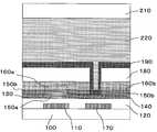
제2 실시 형태의 화상 표시 장치는, 도 8이나 도 10에 일례를 도시한 바와 같이, 상기 구성의 박막 트랜지스터 상에, 적어도 층간 절연층 (180), 화소 전극 (190), 전기 영동체 (220), 및 대향 전극 (210)이 배치되어 구성되어 있다.8 and 10, the image display apparatus of the second embodiment includes at least an interlayer insulating
층간 절연층 (180)은 진공 증착법, 이온 플레이팅법, 스퍼터링법, 레이저 어블레이션법, 플라즈마 CVD, 광 CVD, 핫와이어 CVD법 등의 드라이 제막이나, 스핀 코팅법, 침지 코팅법, 스크린 인쇄법 등의 웨트 성막법을 재료에 따라서 적절하게 사용하여 형성된다. 층간 절연층 (180)은 드레인 전극 (140) 상에 개구부를 갖고 있고, 이 개구부를 통해, 드레인 전극 (140)과 화소 전극 (190)을 접속시킬 수 있다. 개구부는 층간 절연층 (180)의 형성과 동시 또는 형성 후에 포토리소그래피법이나 에칭 등의 공지된 방법을 이용하여 설치할 수 있다.The interlayer insulating
그 층간 절연층 (180) 상에 도전성 재료를 성막하고, 소정의 화소 형상으로 패터닝하여 화소 전극 (190)을 형성한다. 드레인 전극 (140)이 노출되도록 개구부가 형성되어 있는 상기 층간 절연층 (180) 상에 화소 전극 (190)을 형성함으로써 드레인 전극 (140)과 화소 전극 (190)의 도통을 취할 수 있다.A conductive material is formed on the
또한, 상기 화소 전극 (190) 상에, 전기 영동체 (220)을 개재하여 대향 전극 (210)을 설치한다. 전기 영동체 (220)은 전기 영동 방식을 이용한 화상 표시 매체이다.In addition, the
각 전극 및 절연성 보호층의 패터닝 방법으로서는, 공지 일반의 방법을 사용할 수 있다. 예를 들면, 포토리소그래피법을 이용하여 패턴 형성 부분을 레지스트 등에 의해 보호하고, 에칭에 의해서 불필요 부분을 제거하여 행할 수 있지만, 이 방법에 한정되지 않다.As a method of patterning each of the electrodes and the insulating protective layer, a known general method can be used. For example, the pattern forming portion is protected by a resist or the like using a photolithography method, and the unnecessary portion is removed by etching. However, the present invention is not limited to this method.
(제2 실시 형태의 효과)(Effects of the Second Embodiment)
이하, 제2 실시 형태의 효과를 열거한다.Hereinafter, the effects of the second embodiment will be listed.
제2 실시 형태의 박막 트랜지스터 및 박막 트랜지스터의 제조 방법이면, 금속 산화물층 (150)의 패터닝 공정, 특히, 습식 에칭 공정을 생략하는 것이 가능해지기 때문에, 박막 트랜지스터의 제조 공정을 간략화하는 것이 가능해진다.In the method of manufacturing the thin film transistor and the thin film transistor of the second embodiment, it is possible to omit the step of patterning the metal oxide layer 150, in particular, the wet etching step, so that the manufacturing process of the thin film transistor can be simplified.
이에 따라, 고품질 또한 저비용으로 제조가 가능한 박막 트랜지스터 및 그의 제조 방법과, 박막 트랜지스터를 구비하는 화상 표시 장치를 제공하는 것이 가능해진다.Thus, it is possible to provide a thin film transistor which can be manufactured with high quality and low cost, a method of manufacturing the same, and an image display apparatus including the thin film transistor.
<변형예><Modifications>
이하, 제1 실시 형태 및 제2 실시 형태의 변형예를 열거한다.Modifications of the first embodiment and the second embodiment will be enumerated below.
(1) 제1, 제2 실시 형태의 박막 트랜지스터에서는, 반도체 영역의 도전율을 10-7 S/cm 이상 10-3 S/cm 이하의 범위 내로 하고, 절연 영역의 도전율을 10-7 S/cm 미만으로 했지만, 반도체 영역 및 절연 영역의 도전율은 상기한 값에 한정하는 것은 아니다.(1) In the thin film transistors of the first and second embodiments, the conductivity of the semiconductor region is set within the range of 10-7 S / cm to 10-3 S / cm, and the conductivity of the insulating region is set to 10-7 S / cm However, the conductivity of the semiconductor region and the insulating region is not limited to the above value.
(2) 제1, 제2 실시 형태의 박막 트랜지스터에서는, 금속 산화물 재료를, 인듐, 아연, 갈륨 중 어느 하나를 포함하는 것으로 했지만, 금속 산화물 재료의 구성은 이것에 한정하는 것은 아니다.(2) In the thin film transistors of the first and second embodiments, the metal oxide material includes any one of indium, zinc, and gallium, but the structure of the metal oxide material is not limited thereto.
(3) 제1, 제2 실시 형태의 박막 트랜지스터에서는, 절연 기판을 수지 기판으로 했지만, 절연 기판의 구성은 이것에 한정하는 것은 아니다.(3) In the thin film transistors of the first and second embodiments, the insulating substrate is a resin substrate, but the structure of the insulating substrate is not limited thereto.
(4) 제1 실시 형태의 박막 트랜지스터의 제조 방법에서는, 제2 게이트 절연층 (6b)를 CVD법으로 형성한 산화실리콘을 이용하여 형성했지만, 이것에 한정하는 것은 아니고, 제2 게이트 절연층 (6b)를 CVD법으로 형성한 산화실리콘 이외의 것을 이용하여 형성할 수도 있다. 또한, 제1 실시 형태의 박막 트랜지스터 (1)의 제조 방법에서는, 제2 게이트 절연층 (6b)를 산화실리콘, 질화실리콘, 실리콘옥시니트라이드, 산화알루미늄 중 어느 하나의 화합물을 포함한 층으로 했지만, 이것에 한정하는 것은 아니고, 제2 게이트 절연층 (6b)를 상술한 화합물을 포함하지 않는 층으로 할 수도 있다.(4) In the method of manufacturing the thin film transistor of the first embodiment, the second
(5) 제2 실시 형태의 박막 트랜지스터의 제조 방법에서는, 제2 절연성 보호층을 CVD법으로 형성한 산화실리콘을 이용하여 형성했지만, 이것에 한정하는 것은 아니고, 제2 절연성 보호층을 CVD법으로 형성한 산화실리콘 이외의 것을 이용하여 형성할 수도 있다. 또한, 제2 실시 형태의 박막 트랜지스터의 제조 방법에서는, 제2 절연성 보호층을 산화실리콘, 질화실리콘, 실리콘옥시니트라이드, 산화알루미늄 중 어느 하나의 화합물을 포함한 층으로 했지만, 이것에 한정하는 것은 아니고, 제2 절연성 보호층을 상술한 화합물을 포함하지 않는 층으로 할 수도 있다.(5) In the method of manufacturing the thin film transistor according to the second embodiment, the second insulating protection layer is formed using silicon oxide formed by the CVD method. However, the second insulating protection layer is not limited to this, Or may be formed using a material other than the formed silicon oxide. In the method of manufacturing the thin film transistor of the second embodiment, the second insulating protection layer is a layer containing any one of silicon oxide, silicon nitride, silicon oxynitride, and aluminum oxide. However, the present invention is not limited thereto , And the second insulating protective layer may be a layer not containing the above-described compound.
(6) 제1 실시 형태의 박막 트랜지스터에서는 바텀 게이트·톱 콘택트형인 경우, 제2 실시 형태의 박막 트랜지스터에서는 바텀 게이트·바텀 컨택트형인 경우를 설명했지만, 이것에 한정하는 것은 아니고, 게이트 절연층 또는 절연성 보호층에 의해 금속 산화물층이 반도체 영역과 절연체 영역을 가질 수 있으면 되고, 절연 기판, 소스·드레인 전극, 금속 산화물층, 게이트 절연층, 게이트 전극의 순서로 적층한 톱 게이트·바텀 컨택트형일 수도 있고, 절연 기판, 절연성 보호층, 금속 산화물층, 소스·드레인 전극, 게이트 절연층, 게이트 전극의 순서로 적층한 톱 게이트·톱 콘택트형으로 할 수도 있다.(6) In the case of the bottom gate / top contact type in the thin film transistor of the first embodiment, the case of the bottom gate / bottom contact type in the case of the thin film transistor of the second embodiment has been described. However, The metal oxide layer may have a semiconductor region and an insulator region by the protective layer and may be a top gate bottom contact type laminated in this order of an insulating substrate, a source / drain electrode, a metal oxide layer, a gate insulating layer and a gate electrode , An insulating substrate, an insulating protective layer, a metal oxide layer, a source / drain electrode, a gate insulating layer, and a gate electrode may be stacked in this order.
(7) 제1, 제2 실시 형태의 박막 트랜지스터를 구비하는 화상 표시 장치에서는, 화상 표시 매체를 전기 영동 방식의 표시 매체로 했지만, 이것에 한정하는 것은 아니고, 화상 표시 매체를 전기 영동 방식 이외의 표시 매체로 할 수도 있다.(7) In the image display apparatus including the thin film transistors of the first and second embodiments, the image display medium is an electrophoretic display medium. However, the image display medium is not limited to the electrophoretic display medium. It may be a display medium.
[실시예][Example]
이하, 본 발명에 따른 실시 형태에 대해서, 실시예와 비교예를 이용하여 설명한다.Hereinafter, embodiments according to the present invention will be described with reference to examples and comparative examples.
(제1 실시 형태의 실시예)(Embodiment of the First Embodiment)
이하, 도 1을 참조하면서, 도 2부터 도 5를 이용하여, 3 종류의 제1 실시 형태의 박막 트랜지스터 (1)과, 3 종류의 비교예의 박막 트랜지스터 (1)을 제조하고, 양자에 관한 물성의 평가를 행한 결과에 대해서 설명한다.The
(실시예 1)(Example 1)
실시예 1의 박막 트랜지스터 (1)로서는, 도 2 중에 도시하는 박막 트랜지스터 (1)(박막 트랜지스터 소자)을 제조하였다. 또한, 도 2는 실시예에서의 박막 트랜지스터 (1)의 개략 구성을 도시하는 단면도이다.As the
실시예 1의 박막 트랜지스터 (1)을 제조하는 때에는, 절연 기판 (2)로서 PEN 기재(두께 125 ㎛) 상에, DC 마그네트론 스퍼터 장치를 이용하여, Mo를 80 nm의 막 두께로 실온에서 성막하였다.When the
다음으로, 포토리소그래피법을 이용하여 레지스트 패턴을 형성한 후에, 드라이 에칭, 박리를 행하여 게이트 전극 (4)와 캐패시터 전극 (18)을 형성하였다.Next, a resist pattern is formed by photolithography, and dry etching and peeling are performed to form the
여기서, Mo 성막 시의 투입 전력은 100 W로 하고, 가스 유량은 Ar=50 SCCM으로 하고, 성막 압력은 1.0 Pa로 하였다.Here, the input power at the time of forming the Mo film was 100 W, the gas flow rate was Ar = 50 SCCM, and the film forming pressure was 1.0 Pa.
다음으로, 플라즈마 CVD 장치를 이용하여, SiNx를 500 nm의 막 두께로 성막하고, 포토리소그래피법을 이용하여 레지스트 패턴을 형성한 후에, 드라이 에칭, 박리를 행하여 제1 게이트 절연층 (6a)를 형성하였다.Next, a SiNx film having a film thickness of 500 nm is formed by using a plasma CVD apparatus, a resist pattern is formed by photolithography, dry etching and peeling are performed to form a first
여기서, 원료 가스로서, SiH4=10 SCCM, NH3=5 SCCM을 흘리고, 투입 전력을 200 W로 하고, 성막 압력을 3 Pa로 하여, 기판 온도 150℃에서 성막하였다.Here, SiH4 = 10 SCCM and NH3 = 5 SCCM were flowed as a raw material gas, deposition power was 200 W, deposition pressure was 3 Pa, and substrate temperature was 150 캜.
다음으로, 플라즈마 CVD 장치를 이용하여, SiOx를 500 nm의 막 두께로 성막하고, 포토리소그래피법을 이용하여 레지스트 패턴을 형성한 후에, 드라이 에칭, 박리를 행하여 제2 게이트 절연층 (6b)를 형성하였다.Next, a SiOx film is formed to a thickness of 500 nm using a plasma CVD apparatus, a resist pattern is formed by photolithography, dry etching and peeling are performed to form a second
여기서, 원료 가스로서, SiH4=10 SCCM, N2O=10 SCCM을 흘리고, 투입 전력을 300 W로 하고, 성막 압력을 1 Pa로 하여, 기판 온도를 150℃에서 성막하였다.Here, SiH4 = 10 SCCM and N2 O = 10 SCCM were flowed as a raw material gas, the input power was 300 W, the film forming pressure was 1 Pa, and the substrate temperature was 150 캜.
다음으로, 스퍼터링법을 이용하여, InGaZnO를 포함하는 금속 산화물층 (16)을 40 nm의 막 두께로 실온에서 성막하였다.Next, a
여기서, 성막 시의 투입 전력은 100 W이고, 가스 유량은 Ar=100 SCCM이고, O2=2 SCCM, 성막 압력은 1.0 Pa로 하였다.Here, the input power at the time of film formation was 100 W, the gas flow rate was Ar = 100 SCCM, O2 = 2 SCCM, and the deposition pressure was 1.0 Pa.
마지막으로, DC 마그네트론 스퍼터 장치를 이용하여, Mo를 80 nm의 막 두께로 실온에서 성막하고, 포토리소그래피법을 이용하여 레지스트 패턴을 형성한 후에, 드라이 에칭, 박리를 행하여, 소스 전극 (12)와 드레인 전극 (14)를 형성하여, 실시예 1의 박막 트랜지스터 (1)을 얻었다.Finally, a film of Mo is formed at a room temperature with a film thickness of 80 nm using a DC magnetron sputtering apparatus, a resist pattern is formed by photolithography, and then dry etching and peeling are performed to form the
여기서, 소스 전극 (12)와 드레인 전극 (14) 사이의 길이는 20 ㎛이고, 소스 전극 (12)와 드레인 전극 (14) 사이의 폭은 5 ㎛이다.The length between the
상기한 바와 같이 제조한 실시예 1의 박막 트랜지스터 (1)에 대하여 SIMS(이차 이온 질량 분석 장치)를 이용하여 측정한, 제1 게이트 절연층 (6a) 중의 수소 원자의 농도는 5.2×10²¹/cm3이고, 제2 게이트 절연층 (6b) 중의 수소 원자의 농도는 9.0×10¹⁹/cm3였다.The concentration of hydrogen atoms in the first
또한, 반도체 파라미터 애널라이저를 이용하여 측정한, 박막 트랜지스터 (1)의 금속 산화물층 (16)의 반도체 영역 (8)의 도전율은 1.7×10⁻⁴ S/cm이고, 절연 영역 (10)의 도전율은 9.0×10⁻¹⁰ S/cm였다.The conductivity of the
또한, 박막 트랜지스터 (1)의 이동도는 11 cm2/Vs이고, 소스 전극 (12)와 드레인 전극 (14) 사이에 10 V의 전압이 인가되었을 때의 ON/OFF비는 5 자릿수이고, 문턱전압이하 스윙치(s치)는 1.1 V/10년이었다.Further, a mobility of the
이상의 측정 결과로부터, 실시예 1의 박막 트랜지스터 (1)은 양호한 트랜지스터 특성을 나타내는 것이 확인되었다.From the above measurement results, it was confirmed that the
다음으로, 상기와 동일한 방법을 이용하여, 소스 전극 (12)와 드레인 전극 (14)까지 형성한 박막 트랜지스터 (1)에 대하여 도 3에 도시한 바와 같이, 소스 전극 (12) 및 드레인 전극 (14) 상에 SiOx를 포함하는 밀봉층 (20)과, 중합체를 포함하는 층간 절연층 (22)와, ITO를 포함하는 화소 전극 (24)를 형성하여 박막 트랜지스터 어레이 기판 (26)(박막 트랜지스터 어레이)을 얻었다. 또한, 도 3은 실시예에서의 박막 트랜지스터 어레이 기판 (26)의 개략 구성을 도시하는 단면도이다.3, the
이 박막 트랜지스터 어레이 기판 (26)은 일 화소의 크기가 125 ㎛×125 ㎛이고, 이 화소가 480×640개 있는 것이다.The thin film
다음으로, 도 4 중에 도시한 바와 같은 화상 표시 장치 (28)을 박막 트랜지스터 어레이 기판 (26)과, 대향 전극 (30) 사이에 전기 영동 매체 (32)를 사이에 끼워 제작하고, 구동을 행한 바, 양호한 표시가 가능한 것이 확인되었다. 또한, 도 4는 실시예에서의 화상 표시 장치 (28)의 개략 구성을 도시하는 단면도이다.Next, an
(실시예 2)(Example 2)
실시예 2의 박막 트랜지스터 (1)로서는, 제2 게이트 절연층 (6b)로서, 스퍼터 장치를 이용하여 SiNx를 형성한 것 이외에는, 실시예 1과 동일하게, 도 2 중에 도시하는 구성의 박막 트랜지스터 (1)을 제조하였다.The
여기서, SiNx의 성막 시에 있어서의 투입 전력은 500 W로 하고, 가스 유량은 Ar=50 SCCM으로 하고, 성막 압력은 1.0 Pa로 하였다.Here, the input power at the time of forming SiNx was 500 W, the gas flow rate was Ar = 50 SCCM, and the film forming pressure was 1.0 Pa.
상기한 바와 같이 제조한 실시예 2의 박막 트랜지스터 (1)에 대하여 SIMS(이차 이온 질량 분석 장치)를 이용하여 측정한, 제1 게이트 절연층 (6a) 중의 수소 원자의 농도는 5.1×10²¹/cm3이고, 제2 게이트 절연층 (6b) 중의 수소 원자의 농도는 8.1×10¹⁹/cm3였다.The concentration of hydrogen atoms in the first
또한, 반도체 파라미터 애널라이저를 이용하여 측정한, 박막 트랜지스터 (1)의 금속 산화물층 (16)의 반도체 영역 (8)의 도전율은 1.1×10⁻⁴ S/cm이고, 절연 영역 (10)의 도전율은 5.5×10⁻¹⁰ S/cm였다.The conductivity of the
또한, 박막 트랜지스터 (1)의 이동도는 9 cm2/Vs이고, 소스 전극 (12)와 드레인 전극 (14) 사이에 10 V의 전압이 인가되었을 때의 ON/OFF비는 6 자릿수이고, 문턱전압이하 스윙치(s치)는 0.9 V/10년이었다.Further, a thin film transistor (1) mobility is 9 cm2 / Vs, and the voltage of 10 V ON / OFF ratio was six digits of the time is applied between the
이상의 측정 결과로부터, 실시예 2의 박막 트랜지스터 (1)은 양호한 트랜지스터 특성을 나타내는 것이 확인되었다.From the above measurement results, it was confirmed that the
다음으로, 상기와 동일한 방법을 이용하여, 소스 전극 (12)와 드레인 전극 (14)까지 형성한 박막 트랜지스터 (1)에 대하여 도 3 중에 도시한 바와 같이, 소스 전극 (12) 및 드레인 전극 (14) 상에, SiOx를 포함하는 밀봉층 (20)과, 중합체를 포함하는 층간 절연층 (22)와, ITO를 포함하는 화소 전극 (24)를 형성하여 박막 트랜지스터 어레이 기판 (26)을 얻었다.Next, as shown in FIG. 3, the
이 박막 트랜지스터 어레이 기판 (26)은 일 화소의 크기가 125 ㎛×125 ㎛이고, 이 화소가 480×640개 있는 것이다.The thin film
다음으로, 도 4 중에 도시한 바와 같은 화상 표시 장치 (28)을 박막 트랜지스터 어레이 기판 (26)과, 대향 전극 (30) 사이에 전기 영동 매체 (32)를 사이에 끼워 제작하고, 구동을 행한 바, 양호한 표시가 가능한 것이 확인되었다.Next, an
(실시예 3)(Example 3)
실시예 3의 박막 트랜지스터 (1)로서는, 제2 게이트 절연층 (6b)로서, 원자층 퇴적 장치를 이용하여 Al2O3을 형성한 것 이외에는, 실시예 1과 동일하게, 도 2 중에 도시하는 구성의 박막 트랜지스터 (1)을 제조하였다.2, except that Al2 O3 was formed by using an atomic layer deposition apparatus as the second
여기서, Al2O3은 기판 온도를 150℃로 하고, 트리메틸알루미늄과 H2O를 원료로 하여 성막하였다.Here, Al2 O3 was formed by using trimethylaluminum and H2 O as raw materials at a substrate temperature of 150 ° C.
상기한 바와 같이 제조한 실시예 3의 박막 트랜지스터 (1)에 대하여 SIMS(이차 이온 질량 분석 장치)를 이용하여 측정한, 제1 게이트 절연층 (6a) 중의 수소 원자의 농도는 5.0×10²¹/cm3이고, 제2 게이트 절연층 (6b) 중의 수소 원자의 농도는 4.0×10¹⁹/cm3였다.The concentration of hydrogen atoms in the first
또한, 반도체 파라미터 애널라이저를 이용하여 측정한, 박막 트랜지스터 (1)의 금속 산화물층 (16)의 반도체 영역 (8)의 도전율은 1.2×10⁻⁴ S/cm이고, 절연 영역 (10)의 도전율은 3.1×10⁻¹⁰ S/cm였다.The conductivity of the
또한, 박막 트랜지스터 (1)의 이동도는 10 cm2/Vs이고, 소스 전극 (12)와 드레인 전극 (14) 사이에 10 V의 전압이 인가되었을 때의 ON/OFF비는 6 자릿수이고, 문턱전압이하 스윙치(s치)는 0.9 V/10년이었다.Further, a mobility of the
이상의 측정 결과로부터, 실시예 3의 박막 트랜지스터 (1)은 양호한 트랜지스터 특성을 나타내는 것이 확인되었다.From the above measurement results, it was confirmed that the
다음으로, 상기와 동일한 방법을 이용하여, 소스 전극 (12)와 드레인 전극 (14)까지 형성한 박막 트랜지스터 (1)에 대하여 도 3 중에 도시한 바와 같이, 소스 전극 (12) 및 드레인 전극 (14) 상에, SiOx를 포함하는 밀봉층 (20)과, 중합체를 포함하는 층간 절연층 (22)와, ITO를 포함하는 화소 전극 (24)를 형성하여 박막 트랜지스터 어레이 기판 (26)을 얻었다.Next, as shown in FIG. 3, the
이 박막 트랜지스터 어레이 기판 (26)은 일 화소의 크기가 125 ㎛×125 ㎛이고, 이 화소가 480×640개 있는 것이다.The thin film
다음으로, 도 4 중에 도시한 바와 같은 화상 표시 장치 (28)을 박막 트랜지스터 어레이 기판 (26)과, 대향 전극 (30) 사이에 전기 영동 매체 (32)를 사이에 끼워 제작하고, 구동을 행한 바, 양호한 표시가 가능한 것이 확인되었다.Next, an
(비교예 1)(Comparative Example 1)
비교예 1의 박막 트랜지스터 (1)로서는, 게이트 절연층 (6)을 상기한 제2 게이트 절연층 (6b)와 동일한 조건으로 형성하고, 금속 산화물층 (16)을 상기한 반도체 영역 (8)과 동일한 조건으로 형성한 것 이외에는, 실시예 1과 동일한 방법을 이용하여 도 5 중에 도시하는 구성의 박막 트랜지스터 (1)을 제조하였다. 또한, 도 5는 실시예에서의 박막 트랜지스터 (1)의 개략 구성을 도시하는 단면도이다.As the
상기한 바와 같이 제조한 비교예 1의 박막 트랜지스터 (1)에 대하여 SIMS(이차 이온 질량 분석 장치)를 이용하여 측정한, 게이트 절연층 (6) 중의 수소 원자의 농도는 9.2×10¹⁹/cm3였다.The concentration of hydrogen atoms in the
또한, 반도체 파라미터 애널라이저를 이용하여 측정한, 박막 트랜지스터 (1)의 금속 산화물층 (16)의 도전율은 9.1×10⁻¹⁰ S/cm였다.The conductivity of the
또한, 박막 트랜지스터 (1)의 트랜지스터 특성을 측정한 결과, 온 상태에서의 전류치가 작았다.Further, as a result of measuring the transistor characteristics of the
이상의 측정 결과로부터, 비교예 1의 박막 트랜지스터 (1)은 양호한 트랜지스터 특성을 얻을 수 없는 것이 확인되었다.From the above measurement results, it was confirmed that the
(비교예 2)(Comparative Example 2)
비교예 2의 박막 트랜지스터 (1)로서는, 제1 게이트 절연층 (6a)의 성막 시의 기판 가열 온도를 80℃로 한 이외에는, 실시예 1과 동일하게, 도 2 중에 도시하는 구성의 박막 트랜지스터 (1)을 제조하였다.The
상기한 바와 같이 제조한 비교예 2의 박막 트랜지스터 (1)에 대하여 SIMS(이차 이온 질량 분석 장치)를 이용하여 측정한, 제1 게이트 절연층 (6a) 중의 수소 원자의 농도는 6.0×10²²/cm3이고, 제2 게이트 절연층 (6b) 중의 수소 원자의 농도는 9.0×10¹⁹/cm3였다.The concentration of hydrogen atoms in the first
또한, 반도체 파라미터 애널라이저를 이용하여 측정한, 박막 트랜지스터 (1)의 금속 산화물층 (16)의 반도체 영역 (8)의 도전율은 5.3×10⁻² S/cm이고, 절연 영역 (10)의 도전율은 8.9×10⁻¹⁰ S/cm였다.The conductivity of the
또한, 박막 트랜지스터 (1)의 트랜지스터 특성을 측정한 결과, 온 상태에서의 전류치가 작았다.Further, as a result of measuring the transistor characteristics of the
이상의 측정 결과로부터, 비교예 2의 박막 트랜지스터 (1)은 양호한 트랜지스터 특성을 얻을 수 없는 것이 확인되었다.From the above measurement results, it was confirmed that the
(비교예 3)(Comparative Example 3)
비교예 3의 박막 트랜지스터 (1)로서는, 게이트 절연층 (6)을 상기한 제1 게이트 절연층 (6a)와 동일한 조건으로 형성하고, 금속 산화물층 (16)을 상기한 반도체 영역 (8)과 동일한 조건으로 형성한 것 이외에는, 실시예 1과 동일한 방법을 이용하여, 도 5 중에 도시하는 구성의 박막 트랜지스터 (1)을 제조하였다.As the
상기한 바와 같이 제조한 비교예 3의 박막 트랜지스터 (1)에 대하여 SIMS(이차 이온 질량 분석 장치)를 이용하여 측정한, 게이트 절연층 (6) 중의 수소 원자의 농도는 5.1×10²¹/cm3였다.The concentration of hydrogen atoms in the
또한, 반도체 파라미터 애널라이저를 이용하여 측정한, 박막 트랜지스터 (1)의 금속 산화물층 (16)의 도전율은 1.9×10⁻⁴ S/cm였다.In addition, the conductivity of the
또한, 박막 트랜지스터 (1)의 이동도는 10 cm2/Vs이고, 소스 전극 (12)와 드레인 전극 (14) 사이에 10 V의 전압이 인가되었을 때의 ON/OFF비는 5 자릿수이고, 문턱전압이하 스윙치(s치)는 1.2 V/10년이었다.Further, a thin film transistor (1) mobility is 10 cm2 / Vs, and the voltage of 10 V ON / OFF ratio of 5 digits of when applied between the
이상의 측정 결과로부터, 비교예 3의 박막 트랜지스터 (1)은 양호한 트랜지스터 특성을 나타내는 것이 확인되었다.From the above measurement results, it was confirmed that the
다음으로, 상기와 동일한 방법을 이용하여, 소스 전극 (12)와 드레인 전극 (14)까지 형성한 박막 트랜지스터 (1)에 대하여 도 3 중에 도시한 바와 같이, 소스 전극 (12) 및 드레인 전극 (14) 상에, SiOx를 포함하는 밀봉층 (20)과, 중합체를 포함하는 층간 절연층 (22)와, ITO를 포함하는 화소 전극 (24)를 형성하여 박막 트랜지스터 어레이 기판 (26)을 얻었다.Next, as shown in FIG. 3, the
이 박막 트랜지스터 어레이 기판 (26)은 일 화소의 크기가 125 ㎛×125 ㎛이고, 이 화소가 480×640개 있는 것이다.The thin film
다음으로, 도 4 중에 도시한 바와 같은 화상 표시 장치 (28)을 박막 트랜지스터 어레이 기판 (26)과, 대향 전극 (30) 사이에 전기 영동 매체 (32)를 사이에 끼워 제작하고, 구동을 행한 바, 인접하는 화소 사이에서 전기적 상호 작용이 생겨, 양호한 구동을 할 수 없는 것이 확인되었다.Next, an
(제2 실시 형태의 실시예)(Embodiment of the second embodiment)
다음으로, 도 6을 참조하면서, 도 7부터 도 10을 이용하여, 4 종류의 제2 실시 형태의 박막 트랜지스터 (1)과, 2 종류의 비교예의 박막 트랜지스터 (1)을 제조하여, 양자에 관한 물성의 평가를 행한 결과에 대해서 설명한다.Next, referring to Fig. 6,
(실시예 4)(Example 4)
실시예 4에서는, 도 7에 도시한 바와 같은 박막 트랜지스터 소자, 및 도 8에 도시한 바와 같은 화상 표시 장치를 제작하였다.In the fourth embodiment, a thin film transistor element as shown in Fig. 7 and an image display apparatus as shown in Fig. 8 were produced.
실시예 4의 박막 트랜지스터 소자의 제작은 다음과 같다.The fabrication of the thin film transistor element of Example 4 is as follows.
세정한 PEN 기재(두께 125 ㎛)를 절연 기판 (100)으로 하였다. 절연 기판 (100) 상에 DC 마그네트론 스퍼터 장치를 이용하여 Mo를 100 nm 성막 후, 포토리소그래피법에 의해 게이트 전극 (110), 캐패시터 전극 (170)을 형성하였다. Mo 성막 시의 투입 전력은 100 W, Ar 가스 유량 50 SCCM, 성막 압력 1.0 Pa로 하였다. 포토리소그래피 공정으로서는, Mo막에 감광성 포토레지스트를 도포 후, 포토마스크를 통해 노광을 행하고, 현상액에 의해 레지스트 패턴을 형성하고, 에칭에 의해 게이트 패턴을 형성 후, 레지스트 박리를 행하였다. 다음으로 플라즈마 CVD 장치를 이용하여 SiOx를 500 nm 성막하여 게이트 절연막 (120)으로 하였다. SiOx 성막 시의 투입 전력은 300 W, SiH4 가스 유량 10 SCCM, N2O 가스 유량 10 SCCM, 성막 압력 1.0 Pa, 기판 온도 150℃로 하였다. 다음으로 DC 마그네트론 스퍼터 장치를 이용하여 Mo를 100 nm 성막 후, 포토리소그래피법을 이용하여 소스 전극 (130), 드레인 전극 (140)을 형성하였다. Mo 성막 조건, 포토리소그래피 공정은 게이트 전극 (110)의 형성과 같다. 소스/드레인 전극 사이의 길이는 20 ㎛, 소스/드레인 사이의 전극의 폭은 5 ㎛로 하였다. 다음으로 스퍼터링법에 의해 InGaZnO를 포함하는 금속 산화물층 (150)을 40 nm 실온 성막하였다. 투입 전력은 100 W, Ar 가스 유량 100 SCCM, O2 가스 유량 2 SCCM, 성막 압력 1.0 Pa로 하였다. 다음으로 플라즈마 CVD 장치를 이용하여 SiOx를 80 nm 성막하였다. SiOx 성막 시의 투입 전력은 300 W, SiH4 가스 유량 10 SCCM, N2O 가스 유량 10 SCCM, 성막 압력 1.0 Pa, 기판 온도 150℃로 하였다. 성막 후, 포토리소그래피법을 이용하여 레지스트 패턴을 형성하고, 드라이 에칭, 박리에 의해서 절연성 보호층 (160b)를 형성하였다. 마지막으로 플라즈마 CVD 장치를 이용하여 SiNx를 80 nm 성막하여 절연성 보호층 (160a)를 형성하여, 도 7에 도시한 바와 같은 박막 트랜지스터 소자를 얻었다. SiNx 성막 시의 투입 전력 200 W, SiH4 가스 유량 10 SCCM, NH3 가스 유량 5 SCCM, 성막 압력 3.0 Pa, 기판 온도 150℃로 하였다.The cleaned PEN substrate (thickness: 125 탆) was used as the insulating
그리고, 상기한 바와 같이 제작한 실시예 4의 박막 트랜지스터 소자의 절연성 보호층 (160a), (160b)의 수소 원자 농도를 SIMS(이차 이온 질량 분석 장치)를 이용하여 측정하였다.Then, the hydrogen atom concentrations of the insulating
그 결과, 절연성 보호층 (160a)의 수소 원자 농도는 4.8×10²¹/cm3, 절연성 보호층 (160b)의 수소 원자 농도는 8.2×10¹⁹/cm3였다. 또한 금속 산화물층의 반도체 영역 (150a) 및 절연체 영역 (150b)의 도전율을 반도체 파라미터 애널라이저를 이용하여 측정하였다. 그 결과, 반도체 영역 (150a)의 도전율은 2.0×10⁻⁴ S/cm이고, 절연체 영역 (150b)의 도전율은 9.0×10⁻¹⁰ S/cm였다. 또한, 제작한 박막 트랜지스터 소자의 이동도는 9 cm2/Vs, 소스-드레인 전극 사이에 10 V의 전압이 인가되었을 때의 ON/OFF비는 5 자릿수, 문턱전압이하 스윙치(S치)는 1.2 V/10년으로서, 양호한 트랜지스터 특성을 나타내었다.As a result, the hydrogen atom concentration of the insulating
또한 실시예 4의 화상 표시 장치의 제작은 다음과 같다.The fabrication of the image display device of the fourth embodiment is as follows.
상기한 바와 같은 실시예 4의 박막 트랜지스터 소자와 동일한 방법으로 절연성 보호층까지 형성하고, 그 위에 중합체를 포함하는 층간 절연층 (180)을 형성 후, 드라이 에칭에 의해서 비어를 형성하여, ITO를 포함하는 화소 전극 (190)을 형성하였다. 화소 전극 (190)까지 제작한 박막 트랜지스터(크기: 125 ㎛×125 ㎛)가 480개×640개 배열된 것을 박막 트랜지스터 어레이 기판으로 하여, 대향 전극 (210)과의 사이에 전기 영동체 (22)를 개삽하여, 도 8에 도시한 바와 같은, 실시예 4의 화상 표시 장치로 하였다.An insulating protective layer was formed in the same manner as the thin film transistor element of Example 4 described above, and an interlayer insulating
이 실시예 4의 화상 표시 장치의 구동을 행한 바, 양호하게 표시되는 것이 확인되었다.When the image display apparatus of the fourth embodiment was driven, it was confirmed that it was displayed satisfactorily.
(실시예 5)(Example 5)
실시예 5의 박막 트랜지스터 소자에서는, 실시예 4의 박막 트랜지스터 소자와 동일한 절차로 소스 전극 (130), 드레인 전극 (140)까지 형성하고, 그 후, 스퍼터링법에 의해 InGaZnO를 포함하는 금속 산화물층 (150)을 40 nm 실온 성막하였다. 투입 전력은 100 W, Ar 가스 유량 100 SCCM, O2 가스 유량 3 SCCM, 성막 압력 1.0 Pa로 하였다. 다음으로 리프트오프법을 이용하여 절연성 보호층 (160a)를 형성하였다. 금속 산화물층 (150) 상에 레지스트 패턴 형성 후, 플라즈마 CVD 장치를 이용하여 SiNx를 80 nm 성막하였다. SiNx 성막 시의 투입 전력은 300 W, SiH4 가스 유량 10 SCCM, N2O 가스 유량 10 SCCM, 성막 압력 1.0 Pa, 기판 온도 150℃로 하였다. 성막 후, 레지스트를 박리하여 절연성 보호층 (160a)를 형성하였다. 마지막으로 플라즈마 CVD 장치를 이용하여 SiO2를 80 nm 성막하여 절연성 보호층 (160b)를 형성하였다. 이상에 의해, 도 9에 도시한 바와 같은 박막 트랜지스터 소자를 제작하였다. 또한, SiNx 성막 시의 투입 전력 200 W, SiH4 가스 유량 10 SCCM, NH3 가스 유량 5 SCCM, 성막 압력 3.0 Pa, 기판 온도 150℃로 하였다.In the thin film transistor element of Example 5, the
제작한 실시예 5의 박막 트랜지스터 소자의 절연성 보호층 (160a), (160b)의 수소 원자 농도를 SIMS(이차 이온 질량 분석 장치)를 이용하여 측정하였다. 그 결과, 절연성 보호층 (160a)의 수소 원자 농도는 4.7×10²¹/cm3, 절연성 보호층 (160b)의 수소 원자 농도는 8.0×10¹⁹/cm3였다. 또한 금속 산화물층의 반도체 영역 (150a) 및 절연체 영역 (150b)의 도전율을 반도체 파라미터 애널라이저를 이용하여 측정하였다. 그 결과, 반도체 영역 (150a)의 도전율은 2.4×10⁻⁴ S/cm이고, 절연체 영역 (150b)의 도전율은 5.0×10⁻¹⁰ S/cm였다. 또한, 실시예 5의 박막 트랜지스터 소자의 이동도는 9 cm2/Vs, 소스-드레인 전극 사이에 10 V의 전압이 인가되었을 때의 ON/OFF비는 5 자릿수, 문턱전압이하 스윙치(S치)는 0.9 V/10년으로서, 양호한 트랜지스터 특성을 나타내었다.The hydrogen atom concentrations of the insulating
또한 실시예 5의 화상 표시 장치의 제작은 다음과 같다. 즉, 상기 박막 트랜지스터 소자와 동일한 방법으로 절연성 보호층까지 형성하고, 그 위에 중합체를 포함하는 층간 절연층 (180)을 형성하고, 드라이 에칭에 의해서 비어를 형성 후, ITO를 포함하는 화소 전극 (190)을 형성하였다. 화소 전극 (190)까지 제작한 박막 트랜지스터(크기: 125 ㎛×125 ㎛)가 480개×640개 배열된 것을 박막 트랜지스터 어레이 기판으로 하여, 대향 전극 (210)과의 사이에 전기 영동체 (220)을 끼웠다. 이것에 의해서, 도 10에 도시한 바와 같은 화상 표시 장치 (200)을 제작하였다. 그리고, 그 제작한 실시예 5의 화상 표시 장치의 구동을 행한 바, 양호하게 표시되는 것이 확인되었다.The fabrication of the image display device according to the fifth embodiment is as follows. That is, an insulating protective layer is formed in the same manner as the thin film transistor element, an
(실시예 6)(Example 6)
실시예 6에서는, 제2 절연성 보호층 (160b)가 스퍼터링법에 의해 성막된 SiO2막 80 nm인 것을 제외하고, 실시예 4와 동일한 절차로 제작하여, 도 7과 동일 구조를 갖는 박막 트랜지스터 소자를 얻었다. 또한, SiO2 성막 시에는 투입 전력 500 W, Ar 가스 유량 50 SCCM, 성막 압력 1.0 Pa로 하였다.In Example 6, the same procedure as in Example 4 was performed except that the SiO2 film formed by the sputtering method was 80 nm in the second insulating
이 실시예 6의 박막 트랜지스터 소자의 절연성 보호층 (160a), (160b)의 수소 원자 농도를 SIMS(이차 이온 질량 분석 장치)를 이용하여 측정하였다. 그 결과, 절연성 보호층 (160a)의 수소 원자 농도는 4.2×10²¹/cm3, 절연성 보호층 (160b)의 수소 원자 농도는 7.9×10¹⁹/cm3였다. 또한 금속 산화물층의 반도체 영역 (150a) 및 절연체 영역 (150b)의 도전율을 반도체 파라미터 애널라이저를 이용하여 측정한 결과, 반도체 영역 (150a)의 도전율은 1.9×10⁻⁴ S/cm이고, 절연체 영역 (150b)의 도전율은 6.0×10⁻¹⁰ S/cm였다. 박막 트랜지스터 소자의 이동도는 8 cm2/Vs, 소스-드레인 전극 사이에 10 V의 전압이 인가되었을 때의 ON/OFF비는 5 자릿수, 문턱전압이하 스윙치(S치)는 1.3 V/10년으로서, 양호한 트랜지스터 특성을 나타내었다.The hydrogen atom concentrations of the insulating
또한 실시예 6의 화상 표시 장치의 제작은 다음과 같다. 즉, 실시예 6의 박막 트랜지스터 소자와 동일한 방법으로 절연성 보호층까지 형성하고, 그 위에 중합체를 포함하는 층간 절연층 (180)을 형성하고, 드라이 에칭에 의해서 비어를 형성 후, ITO를 포함하는 화소 전극 (190)을 형성하였다. 화소 전극 (190)까지 제작한 박막 트랜지스터(크기: 125 ㎛×125 ㎛)를 480개×640개 배열된 박막 트랜지스터 어레이 기판으로 하여, 대향 전극 (210)과의 사이에 전기 영동체 (220)을 개삽하였다. 이와 같이 하여 실시예 6의 화상 표시 장치를 제작하였다.The image display device of Example 6 is fabricated as follows. That is, an insulating protective layer is formed in the same manner as the thin film transistor element of Example 6, an
제작한 실시예 6의 화상 표시 장치의 구조는 도 8에 도시하는 것과 동일하다. 이 실시예 6의 화상 표시 장치의 구동을 행한 바, 양호하게 표시되는 것이 확인되었다.The structure of the manufactured image display apparatus of the sixth embodiment is the same as that shown in Fig. When the image display apparatus of Example 6 was driven, it was confirmed that it was displayed satisfactorily.
(실시예 7)(Example 7)
박막 트랜지스터 소자에 있어서 제2 절연성 보호층 (160b)가 스퍼터 장치에 의한 원자 퇴적법을 이용하여 성막된 Al2O3 80 nm인 것을 제외하고, 도 7과 동일 구조를 갖고 실시예 4와 동일한 절차로 제작한 실시예 7의 박막 트랜지스터 소자를 얻었다. 또한, Al2O3은 트리메틸알루미늄과 H2O를 원료로 하여, 기판 온도 150℃에서 성막하였다.7 except that the second insulating
그 실시예 7의 박막 트랜지스터 소자의 절연성 보호층 (160a), (160b)의 수소 원자 농도를 SIMS(이차 이온 질량 분석 장치)를 이용하여 측정하였다. 그 결과, 절연성 보호층 (160a)의 수소 원자 농도는 2.1×10²¹/cm3, 절연성 보호층 (160b)의 수소 원자 농도는 9.1×10¹⁹/cm3였다. 또한 금속 산화물층의 반도체 영역 (150a) 및 절연체 영역 (150b)의 도전율을 반도체 파라미터 애널라이저를 이용하여 측정하였다. 그 결과, 반도체 영역 (150a)의 도전율은 1.7×10⁻⁴ S/cm이고, 절연체 영역 (150b)의 도전율은 4.0×10⁻¹⁰ S/cm였다. 박막 트랜지스터 소자의 이동도는 7 cm2/Vs, 소스-드레인 전극 사이에 10 V의 전압이 인가되었을 때의 ON/OFF비는 5 자릿수, 문턱전압이하 스윙치(S치)는 1.5 V/10년으로서, 양호한 트랜지스터 특성을 나타내었다.The hydrogen atom concentrations of the insulating
또한 실시예 7의 화상 표시 장치의 제작은 다음과 같다. 즉, 실시예 7의 박막 트랜지스터 소자와 동일한 방법으로 절연성 보호층까지 형성하고, 그 위에 중합체를 포함하는 층간 절연층 (180)을 형성하고, 드라이 에칭에 의해서 비어를 형성 후, ITO를 포함하는 화소 전극 (190)을 형성하였다. 화소 전극 (190)까지 제작한 박막 트랜지스터(크기: 125 ㎛×125 ㎛)가 480개×640개 배열된 것을 박막 트랜지스터 어레이로 하여, 대향 전극 (210)과의 사이에 전기 영동체 (220)을 끼웠다. 이와 같이 하여 실시예 7의 화상 표시 장치를 제작하였다.The image display device of Example 7 is fabricated as follows. That is, an insulating protective layer is formed by the same method as that of the thin film transistor element of Example 7, an
이 실시예 7의 화상 표시 장치는, 도 8에 도시하는 것과 동일 구조를 갖는다. 그 실시예 7의 화상 표시 장치의 구동을 행한 바, 양호하게 표시되는 것이 확인되었다.The image display apparatus of the seventh embodiment has the same structure as that shown in Fig. When the image display apparatus of the seventh embodiment was driven, it was confirmed that it was displayed satisfactorily.
(비교예 4)(Comparative Example 4)
도 7에 도시하는 박막 트랜지스터 소자 구조를 갖고, 제2 절연성 보호층 (160b)를 제1 절연성 보호층 (160a)와 동일 조건으로 형성한(즉, 절연성 보호층 (160)을 제1 절연성 보호층 (160a)와 동일 조건으로 성막함) 것 이외에는, 실시예 4와 동일한 절차로 박막 트랜지스터 소자를 제작하고, 비교예 4로 하였다.7, and the second insulating
비교예 4의 박막 트랜지스터 소자의 절연성 보호층 (160a), (160b)의 수소 원자 농도를 SIMS(이차 이온 질량 분석 장치)에 의해 측정하였다. 그 결과, 절연성 보호층 (160a)의 수소 원자 농도는 3.6×10²¹/cm3, 절연성 보호층 (160b)의 수소 원자 농도는 3.8×10²¹/cm3였다. 또한 금속 산화물층의 반도체 영역 (150a) 및 절연체 영역 (150b)의 도전율을 반도체 파라미터 애널라이저를 이용하여 측정하였다. 그 결과, 반도체 영역 (150a)의 도전율은 1.9×10⁻⁴ S/cm이고, 절연체 영역 (150b)의 도전율은 2.0×10⁻⁴ S/cm였다. 이 비교예 4의 박막 트랜지스터 소자의 트랜지스터 특성을 측정한 결과, 오프 상태에서의 전류치가 커서, 트랜지스터 특성은 얻어지지 않았다.The hydrogen atom concentrations of the insulating
(비교예 5)(Comparative Example 5)
도 9에 도시하는 박막 트랜지스터 소자 구조를 갖고, 제1 절연성 보호층 (160a)를 제2 절연성 보호층 (160b)와 동일 조건으로 형성한(즉, 절연성 보호층 (160)을 제2 절연성 보호층 (160b)와 동일 조건으로 성막함) 것 이외에는 실시예 5와 동일한 절차로 박막 트랜지스터 소자를 제작하여 비교예 5를 얻었다.The first insulating
비교예 5의 박막 트랜지스터 소자의 절연성 보호층 (160a), (160b)의 수소 원자 농도를 SIMS(이차 이온 질량 분석 장치)에 의해 측정하였다. 그 결과, 절연성 보호층 (160a)의 수소 원자 농도는 7.0×10¹⁹/cm3, 절연성 보호층 (160b)의 수소 원자 농도는 6.9×10¹⁹/cm3였다. 또한 금속 산화물층의 반도체 영역 (150a) 및 절연체 영역 (150b)의 도전율을 반도체 파라미터 애널라이저에 의해 측정하였다. 그 결과, 반도체 영역 (150a)의 도전율은 8.0×10⁻¹⁰ S/cm이고, 절연체 영역 (150b)의 도전율은 6.8×10⁻¹⁰ S/cm였다. 이 비교예 5의 박막 트랜지스터 소자의 트랜지스터 특성을 측정한 결과, 온 상태에서의 전류치가 작아, 트랜지스터 특성은 얻어지지 않았다.The hydrogen atom concentrations of the insulating
본 발명의 박막 트랜지스터는, 전자 페이퍼, LCD, 유기 EL 디스플레이 등의 스위칭 소자로서 이용할 수 있다. 또한, 특히 전체 공정 중의 온도를 150℃ 이하로 할 수 있어, 반도체층의 패터닝을 생략할 수 있는 점에서, 플렉시블 기재를 기판으로 하는 디바이스를 고작업 처리량, 저비용 또한 고품질로 제작하는 것이 가능해진다. 구체적으로는, 플렉시블 디스플레이나 IC 카드, IC 태그 등에 널리 응용할 수 있다.The thin film transistor of the present invention can be used as a switching element of an electronic paper, an LCD, an organic EL display or the like. In addition, in particular, since the temperature during the whole process can be set to 150 占 폚 or less and the patterning of the semiconductor layer can be omitted, it becomes possible to manufacture a device using a flexible substrate as a substrate with high work throughput, low cost and high quality. Specifically, it can be widely applied to a flexible display, an IC card, an IC tag, and the like.
1: 박막 트랜지스터
2: 절연 기판
4: 게이트 전극
6: 게이트 절연층
6a: 제1 게이트 절연층
6b: 제2 게이트 절연층
8: 반도체 영역
10: 절연 영역
12: 소스 전극
14: 드레인 전극
16: 금속 산화물층
18: 캐패시터 전극
20: 밀봉층
22: 층간 절연층
24: 화소 전극
26: 박막 트랜지스터 어레이 기판
28: 화상 표시 장치
30: 대향 전극
32: 전기 영동 매체
100: 절연 기판
110: 게이트 전극
120: 게이트 절연층
130: 소스 전극
140: 드레인 전극
150: 금속 산화물층
150a: 금속 산화물층의 반도체 영역
150b: 금속 산화물층의 절연체 영역
160: 절연성 보호층
160a: 제1 절연성 보호층
160b: 제2 절연성 보호층
170: 캐패시터 전극
180: 층간 절연층
190: 화소 전극
200: 트랜지스터 어레이 기판
210: 대향 전극
220: 전기 영동체1: Thin film transistor
2: insulating substrate
4: gate electrode
6: Gate insulating layer
6a: a first gate insulating layer
6b: a second gate insulating layer
8: semiconductor region
10: Insulation area
12: source electrode
14: drain electrode
16: metal oxide layer
18: capacitor electrode
20: sealing layer
22: interlayer insulating layer
24:
26: thin film transistor array substrate
28: Image display device
30: opposing electrode
32: electrophoresis medium
100: insulating substrate
110: gate electrode
120: gate insulating layer
130: source electrode
140: drain electrode
150: metal oxide layer
150a: semiconductor region of the metal oxide layer
150b: insulator region of the metal oxide layer
160: insulating protective layer
160a: first insulating protection layer
160b: second insulating protection layer
170: capacitor electrode
180: interlayer insulating layer
190: pixel electrode
200: transistor array substrate
210: counter electrode
220: electrophoresis
Claims (15)
Translated fromKorean상기 반도체 영역은 상기 소스 전극과 드레인 전극 사이의 영역을 포함하고, 또한 상기 소스 전극 및 드레인 전극의 일부와 중첩되어 있고,
상기 반도체 영역은 적어도 상기 게이트 절연층 또는 상기 절연성 보호층 중 어느 하나와 접하도록 상기 게이트 절연층과 상기 절연성 보호층 사이에 형성되고,
상기 절연성 보호층은 상기 소스 전극 및 드레인 전극 상에 형성되며,
상기 게이트 절연층 또는 상기 절연성 보호층의 상기 반도체 영역과 접하는 부분의 수소 원자의 농도는 1×10²⁰/cm3 이상 5×10²²/cm3 이하이고,
상기 게이트 절연층 또는 상기 절연성 보호층의 상기 반도체 영역과 접하지 않은 부분의 수소 원자의 농도는 1×10²⁰/cm3 미만인 것을 특징으로 하는 박막 트랜지스터.There is provided a semiconductor device comprising at least a gate electrode, a gate insulating layer, a source electrode and a drain electrode, a metal oxide layer containing the same metal oxide and having a semiconductor region and an insulating region located on the same plane, A thin film transistor comprising:
Wherein the semiconductor region includes a region between the source electrode and the drain electrode and overlaps with a portion of the source electrode and the drain electrode,
Wherein the semiconductor region is formed between the gate insulating layer and the insulating protective layer so as to be in contact with at least either the gate insulating layer or the insulating protective layer,
Wherein the insulating protective layer is formed on the source electrode and the drain electrode,
Wherein a concentration of hydrogen atoms in a portion of the gate insulating layer or the insulating protective layer that is in contact with the semiconductor region is 1 x 10²⁰ / cm3 to 5 x 10²² / cm3 ,
Wherein a concentration of hydrogen atoms in a portion of the gate insulating layer or the insulating protective layer that is not in contact with the semiconductor region is less than 1 x 10²⁰ / cm3 .
상기 게이트 전극은 상기 절연 기판 상에 설치되고, 상기 게이트 절연층은 상기 게이트 전극 및 상기 절연 기판 상에 설치되고, 상기 금속 산화물층은 상기 게이트 절연층 상에 설치되고, 상기 소스 전극 및 드레인 전극은 상기 반도체 영역과 접속하도록 상기 금속 산화물층 상에 설치되고, 상기 절연성 보호층은 상기 소스 전극, 드레인 전극 및 금속 산화물층 상에 설치되고,
상기 게이트 절연층은, 상기 금속 산화물층의 반도체 영역에 접하는 제1 게이트 절연층과, 상기 금속 산화물층의 절연 영역에 접하는 제2 게이트 절연층을 포함하고,
상기 제1 게이트 절연층 중의 수소 원자의 농도는 1×10²⁰/cm3 이상 5×10²²/cm3 이하이고,
상기 제2 게이트 절연층 중의 수소 원자의 농도는 1×10²⁰/cm3 미만인 것을 특징으로 하는 박막 트랜지스터.The method according to claim 1,
Wherein the gate electrode is provided on the insulating substrate, the gate insulating layer is provided on the gate electrode and the insulating substrate, the metal oxide layer is provided on the gate insulating layer, Wherein the insulating protective layer is provided on the source electrode, the drain electrode, and the metal oxide layer,
Wherein the gate insulating layer includes a first gate insulating layer in contact with a semiconductor region of the metal oxide layer and a second gate insulating layer in contact with an insulating region of the metal oxide layer,
The concentration of hydrogen atoms in the first gate insulating layer is not less than 1 x 10²⁰ / cm3 and not more than 5 x 10²² / cm3 ,
Wherein a concentration of hydrogen atoms in the second gate insulating layer is less than 1 x 10 <20 > / cm <3 >.
상기 게이트 전극은 상기 절연 기판 상에 설치되고, 상기 게이트 절연층은 상기 게이트 전극 및 상기 절연 기판 상에 설치되고, 상기 소스 전극 및 드레인 전극은 상기 게이트 절연층 상에 설치되고, 상기 금속 산화물층은 상기 게이트 절연층, 상기 소스 전극 및 드레인 전극 상에 설치되고, 상기 절연성 보호층은 상기 소스 전극, 드레인 전극 및 금속 산화물층 상에 설치되고,
상기 절연성 보호층은 상기 금속 산화물층의 반도체 영역에 접하는 제1 절연성 보호층과, 상기 금속 산화물층의 절연 영역에 접하는 제2 절연성 보호층을 포함하고,
상기 제1 절연성 보호층 중의 수소 원자의 농도는 1×10²⁰/cm3 이상 5×10²²/cm3 이하이고,
상기 제2 절연성 보호층 중의 수소 원자의 농도는 1×10²⁰/cm3 미만인 것을 특징으로 하는 박막 트랜지스터.The method according to claim 1,
Wherein the gate electrode is provided on the insulating substrate, the gate insulating layer is provided on the gate electrode and the insulating substrate, the source electrode and the drain electrode are provided on the gate insulating layer, The source electrode, and the drain electrode, the insulating protective layer is provided on the source electrode, the drain electrode, and the metal oxide layer,
Wherein the insulating protective layer includes a first insulating protective layer in contact with a semiconductor region of the metal oxide layer and a second insulating protective layer in contact with an insulating region of the metal oxide layer,
The concentration of hydrogen atoms in the first insulating protective layer is not less than 1 x 10²⁰ / cm3 and not more than 5 x 10²² / cm3 ,
And the concentration of hydrogen atoms in the second insulating protection layer is less than 1 x 10 <20 > / cm <3 >.
상기 반도체 영역은 상기 소스 전극과 드레인 전극 사이의 영역을 포함하고, 또한 상기 소스 전극 및 드레인 전극의 일부와 중첩되어 있고,
상기 반도체 영역은 적어도 상기 게이트 절연층 또는 상기 절연성 보호층 중 어느 하나와 접하도록 상기 게이트 절연층과 상기 절연성 보호층 사이에 형성되고,
상기 절연성 보호층은 상기 소스 전극 및 드레인 전극 아래에 형성되며,
상기 게이트 절연층 또는 상기 절연성 보호층의 상기 반도체 영역과 접하는 부분의 수소 원자의 농도는 1×10²⁰/cm3 이상 5×10²²/cm3 이하이고,
상기 게이트 절연층 또는 상기 절연성 보호층의 상기 반도체 영역과 접하지 않은 부분의 수소 원자의 농도는 1×10²⁰/cm3 미만인 것을 특징으로 하는 박막 트랜지스터.There is provided a semiconductor device comprising at least a gate electrode, a gate insulating layer, a source electrode and a drain electrode, a metal oxide layer containing the same metal oxide and having a semiconductor region and an insulating region located on the same plane, A thin film transistor comprising:
Wherein the semiconductor region includes a region between the source electrode and the drain electrode and overlaps with a portion of the source electrode and the drain electrode,
Wherein the semiconductor region is formed between the gate insulating layer and the insulating protective layer so as to be in contact with at least either the gate insulating layer or the insulating protective layer,
Wherein the insulating protective layer is formed below the source electrode and the drain electrode,
Wherein a concentration of hydrogen atoms in a portion of the gate insulating layer or the insulating protective layer that is in contact with the semiconductor region is 1 x 10²⁰ / cm3 to 5 x 10²² / cm3 ,
Wherein a concentration of hydrogen atoms in a portion of the gate insulating layer or the insulating protective layer that is not in contact with the semiconductor region is less than 1 x 10²⁰ / cm3 .
상기 절연 영역의 도전율은 10-7 S/cm 미만인 것을 특징으로 하는 박막 트랜지스터.9. The semiconductor device according to any one of claims 1 to 8, wherein the conductivity of the semiconductor region is in the range of 10-7 S / cm or more and 10-3 S / cm or less,
Wherein a conductivity of the insulating region is less than 10 <-7 > S / cm.
Applications Claiming Priority (5)
| Application Number | Priority Date | Filing Date | Title |
|---|---|---|---|
| JPJP-P-2010-217410 | 2010-09-28 | ||
| JP2010217410 | 2010-09-28 | ||
| JP2011068149 | 2011-03-25 | ||
| JPJP-P-2011-068149 | 2011-03-25 | ||
| PCT/JP2011/071482WO2012043338A1 (en) | 2010-09-28 | 2011-09-21 | Thin film transistor, method for manufacturing same, and image display device provided with thin film transistor |
Publications (2)
| Publication Number | Publication Date |
|---|---|
| KR20130092591A KR20130092591A (en) | 2013-08-20 |
| KR101891841B1true KR101891841B1 (en) | 2018-08-24 |
Family
ID=45892796
Family Applications (1)
| Application Number | Title | Priority Date | Filing Date |
|---|---|---|---|
| KR1020137010750AExpired - Fee RelatedKR101891841B1 (en) | 2010-09-28 | 2011-09-21 | Thin film transistor, method for manufacturing same, and image display device provided with thin film transistor |
Country Status (6)
| Country | Link |
|---|---|
| US (1) | US8963147B2 (en) |
| JP (1) | JPWO2012043338A1 (en) |
| KR (1) | KR101891841B1 (en) |
| CN (1) | CN103140920B (en) |
| TW (1) | TWI542014B (en) |
| WO (1) | WO2012043338A1 (en) |
Families Citing this family (30)
| Publication number | Priority date | Publication date | Assignee | Title |
|---|---|---|---|---|
| TWI613822B (en) | 2011-09-29 | 2018-02-01 | 半導體能源研究所股份有限公司 | Semiconductor device and method of manufacturing same |
| TWI567985B (en)* | 2011-10-21 | 2017-01-21 | 半導體能源研究所股份有限公司 | Semiconductor device and method of manufacturing same |
| KR102099445B1 (en) | 2012-06-29 | 2020-04-09 | 가부시키가이샤 한도오따이 에네루기 켄큐쇼 | Semiconductor device and method for manufacturing semiconductor device |
| WO2014003086A1 (en)* | 2012-06-29 | 2014-01-03 | Semiconductor Energy Laboratory Co., Ltd. | Semiconductor device |
| KR20140026257A (en)* | 2012-08-23 | 2014-03-05 | 가부시키가이샤 한도오따이 에네루기 켄큐쇼 | Display device |
| JP6070073B2 (en)* | 2012-10-31 | 2017-02-01 | 凸版印刷株式会社 | Thin film transistor array |
| TWI597849B (en)* | 2012-12-28 | 2017-09-01 | 神戶製鋼所股份有限公司 | Thin film transistor and method of manufacturing the same |
| JP6108898B2 (en)* | 2013-03-19 | 2017-04-05 | 株式会社東芝 | Display device, thin film transistor, method for manufacturing display device, and method for manufacturing thin film transistor |
| TWI515912B (en)* | 2013-05-08 | 2016-01-01 | 友達光電股份有限公司 | Semiconductor component |
| EP2808916B1 (en)* | 2013-05-30 | 2018-12-12 | LG Display Co., Ltd. | Method of manufacturing an organic light emitting display device |
| JPWO2014196107A1 (en)* | 2013-06-04 | 2017-02-23 | 株式会社Joled | THIN FILM TRANSISTOR ELEMENT, ITS MANUFACTURING METHOD, AND DISPLAY DEVICE |
| JP2015060996A (en)* | 2013-09-19 | 2015-03-30 | 株式会社東芝 | Display device and semiconductor device |
| JP6180908B2 (en)* | 2013-12-06 | 2017-08-16 | 富士フイルム株式会社 | Metal oxide semiconductor film, thin film transistor, display device, image sensor and X-ray sensor |
| FR3024589B1 (en)* | 2014-07-29 | 2017-12-08 | Commissariat Energie Atomique | ELECTRONIC DEVICE AND METHOD FOR MANUFACTURING THE SAME |
| WO2016041179A1 (en)* | 2014-09-18 | 2016-03-24 | 华为技术有限公司 | Material and optical assembly for blocking crosstalk and manufacturing method for material |
| US9985139B2 (en)* | 2014-11-12 | 2018-05-29 | Qualcomm Incorporated | Hydrogenated p-channel metal oxide semiconductor thin film transistors |
| US9685542B2 (en)* | 2014-12-30 | 2017-06-20 | Qualcomm Incorporated | Atomic layer deposition of P-type oxide semiconductor thin films |
| US9647135B2 (en) | 2015-01-22 | 2017-05-09 | Snaptrack, Inc. | Tin based p-type oxide semiconductor and thin film transistor applications |
| JP6611521B2 (en) | 2015-08-25 | 2019-11-27 | 三菱電機株式会社 | Thin film transistor and array substrate |
| KR102643111B1 (en)* | 2016-07-05 | 2024-03-04 | 삼성디스플레이 주식회사 | Thin film transistor, thin film transistor array panel including the same and manufacturing method thereof |
| JP2018157101A (en)* | 2017-03-17 | 2018-10-04 | 東芝メモリ株式会社 | Transistor, memory, and method of manufacturing transistor |
| KR101973269B1 (en)* | 2017-07-31 | 2019-04-26 | 한양대학교 산학협력단 | Oxide Semiconductor Thin Film Transistor and Fabricating Method Thereof |
| TWI648844B (en) | 2017-11-06 | 2019-01-21 | Industrial Technology Research Institute | Thin film transistor and method of manufacturing same |
| CN108089381A (en)* | 2018-01-02 | 2018-05-29 | 京东方科技集团股份有限公司 | Side electrode production method |
| WO2022060700A1 (en) | 2020-09-15 | 2022-03-24 | E Ink Corporation | Improved driving voltages for advanced color electrophoretic displays and displays with improved driving voltages |
| JP7542140B2 (en) | 2020-09-15 | 2024-08-29 | イー インク コーポレイション | Four-particle electrophoretic medium providing fast and high contrast optical state switching |
| US12181767B2 (en) | 2020-09-15 | 2024-12-31 | E Ink Corporation | Five-particle electrophoretic medium with improved black optical state |
| US11846863B2 (en) | 2020-09-15 | 2023-12-19 | E Ink Corporation | Coordinated top electrode—drive electrode voltages for switching optical state of electrophoretic displays using positive and negative voltages of different magnitudes |
| TWI813944B (en)* | 2021-02-08 | 2023-09-01 | 友達光電股份有限公司 | Active device substrate and fabrication method of active device substrate |
| CN114512611B (en)* | 2022-01-18 | 2025-10-03 | 河南师范大学 | Field effect transistor and preparation method thereof |
Citations (1)
| Publication number | Priority date | Publication date | Assignee | Title |
|---|---|---|---|---|
| JP2008235871A (en)* | 2007-02-20 | 2008-10-02 | Canon Inc | Thin film transistor forming method and display device |
Family Cites Families (11)
| Publication number | Priority date | Publication date | Assignee | Title |
|---|---|---|---|---|
| JP3460170B2 (en)* | 1997-02-03 | 2003-10-27 | シャープ株式会社 | Thin film transistor and method of manufacturing the same |
| JP3599972B2 (en)* | 1997-09-30 | 2004-12-08 | 三洋電機株式会社 | Method for manufacturing thin film transistor |
| JP5015471B2 (en)* | 2006-02-15 | 2012-08-29 | 財団法人高知県産業振興センター | Thin film transistor and manufacturing method thereof |
| JP5105842B2 (en) | 2006-12-05 | 2012-12-26 | キヤノン株式会社 | Display device using oxide semiconductor and manufacturing method thereof |
| US8436349B2 (en) | 2007-02-20 | 2013-05-07 | Canon Kabushiki Kaisha | Thin-film transistor fabrication process and display device |
| KR100873081B1 (en)* | 2007-05-29 | 2008-12-09 | 삼성모바일디스플레이주식회사 | Thin film transistor, its manufacturing method, and flat panel display device comprising thin film transistor |
| JP5704790B2 (en)* | 2008-05-07 | 2015-04-22 | キヤノン株式会社 | Thin film transistor and display device |
| JP5403390B2 (en)* | 2008-05-16 | 2014-01-29 | 出光興産株式会社 | Oxides containing indium, gallium and zinc |
| JP5616012B2 (en)* | 2008-10-24 | 2014-10-29 | 株式会社半導体エネルギー研究所 | Method for manufacturing semiconductor device |
| TWI485781B (en)* | 2009-03-13 | 2015-05-21 | Semiconductor Energy Lab | Semiconductor device and method of manufacturing the same |
| US8685787B2 (en)* | 2010-08-25 | 2014-04-01 | Semiconductor Energy Laboratory Co., Ltd. | Manufacturing method of semiconductor device |
- 2011
- 2011-09-21WOPCT/JP2011/071482patent/WO2012043338A1/enactiveApplication Filing
- 2011-09-21USUS13/876,419patent/US8963147B2/ennot_activeExpired - Fee Related
- 2011-09-21JPJP2012536369Apatent/JPWO2012043338A1/ennot_activeWithdrawn
- 2011-09-21KRKR1020137010750Apatent/KR101891841B1/ennot_activeExpired - Fee Related
- 2011-09-21CNCN201180047023.2Apatent/CN103140920B/ennot_activeExpired - Fee Related
- 2011-09-27TWTW100134699Apatent/TWI542014B/ennot_activeIP Right Cessation
Patent Citations (1)
| Publication number | Priority date | Publication date | Assignee | Title |
|---|---|---|---|---|
| JP2008235871A (en)* | 2007-02-20 | 2008-10-02 | Canon Inc | Thin film transistor forming method and display device |
Also Published As
| Publication number | Publication date |
|---|---|
| WO2012043338A1 (en) | 2012-04-05 |
| TWI542014B (en) | 2016-07-11 |
| US8963147B2 (en) | 2015-02-24 |
| JPWO2012043338A1 (en) | 2014-02-06 |
| KR20130092591A (en) | 2013-08-20 |
| US20140217396A1 (en) | 2014-08-07 |
| CN103140920A (en) | 2013-06-05 |
| CN103140920B (en) | 2016-05-04 |
| TW201230342A (en) | 2012-07-16 |
Similar Documents
| Publication | Publication Date | Title |
|---|---|---|
| KR101891841B1 (en) | Thin film transistor, method for manufacturing same, and image display device provided with thin film transistor | |
| JP5250944B2 (en) | Structure, transmissive liquid crystal display device, semiconductor circuit manufacturing method, and transmissive liquid crystal display device manufacturing method | |
| US8487308B2 (en) | Thin film transistor and image display unit | |
| US20190280018A1 (en) | Array substrate, manufacturing method therefor and display device | |
| KR101949538B1 (en) | Thin film transistor, manufacturing method therefor and image display device | |
| WO2014166176A1 (en) | Thin-film transistor and manufacturing method thereof, array base plate and display apparatus | |
| JP2007298627A (en) | Display device and manufacturing method thereof | |
| JP2010087223A (en) | Thin film transistor and active matrix display | |
| WO2013170574A1 (en) | Oxide thin film transistor and manufacturing method thereof, array substrate and display device | |
| JP5655277B2 (en) | Thin film transistor and active matrix display | |
| JP2008076823A (en) | Display device | |
| JP5278637B2 (en) | Structure, transmissive liquid crystal display device, semiconductor circuit manufacturing method, and transmissive liquid crystal display device manufacturing method | |
| TWI594432B (en) | Oxide semiconductor device, method of manufacturing oxide semiconductor device, display device, and image sensor | |
| JP6260326B2 (en) | Thin film transistor device and manufacturing method thereof | |
| US20090213039A1 (en) | Display device | |
| JP5617214B2 (en) | THIN FILM TRANSISTOR, MANUFACTURING METHOD THEREOF, AND IMAGE DISPLAY DEVICE | |
| JP2012204502A (en) | Thin film transistor, manufacturing method of the same and picture display device using thin film transistor | |
| JP5604938B2 (en) | Thin film transistor and manufacturing method thereof | |
| JP5124976B2 (en) | Display device and manufacturing method thereof | |
| WO2014049970A1 (en) | Thin film transistor array and image display apparatus | |
| JP2007298602A (en) | Structure, transmissive liquid crystal display device, semiconductor circuit manufacturing method, and transmissive liquid crystal display device manufacturing method | |
| WO2019078267A1 (en) | Organic thin-film transistor, manufacturing method therefor, active matrix array and image display device | |
| JP6123413B2 (en) | Thin film transistor array and image display device | |
| JP2012204398A (en) | Thin film transistor and manufacturing method therefor, and image display device using thin film transistor | |
| JP2012074596A (en) | Thin-film transistor, image display device having thin-film transistor, method of manufacturing thin-film transistor, and method of manufacturing image display device |
Legal Events
| Date | Code | Title | Description |
|---|---|---|---|
| PA0105 | International application | St.27 status event code:A-0-1-A10-A15-nap-PA0105 | |
| PG1501 | Laying open of application | St.27 status event code:A-1-1-Q10-Q12-nap-PG1501 | |
| A201 | Request for examination | ||
| P11-X000 | Amendment of application requested | St.27 status event code:A-2-2-P10-P11-nap-X000 | |
| P13-X000 | Application amended | St.27 status event code:A-2-2-P10-P13-nap-X000 | |
| PA0201 | Request for examination | St.27 status event code:A-1-2-D10-D11-exm-PA0201 | |
| E902 | Notification of reason for refusal | ||
| PE0902 | Notice of grounds for rejection | St.27 status event code:A-1-2-D10-D21-exm-PE0902 | |
| E13-X000 | Pre-grant limitation requested | St.27 status event code:A-2-3-E10-E13-lim-X000 | |
| P11-X000 | Amendment of application requested | St.27 status event code:A-2-2-P10-P11-nap-X000 | |
| P13-X000 | Application amended | St.27 status event code:A-2-2-P10-P13-nap-X000 | |
| E701 | Decision to grant or registration of patent right | ||
| PE0701 | Decision of registration | St.27 status event code:A-1-2-D10-D22-exm-PE0701 | |
| GRNT | Written decision to grant | ||
| PR0701 | Registration of establishment | St.27 status event code:A-2-4-F10-F11-exm-PR0701 | |
| PR1002 | Payment of registration fee | St.27 status event code:A-2-2-U10-U12-oth-PR1002 Fee payment year number:1 | |
| PG1601 | Publication of registration | St.27 status event code:A-4-4-Q10-Q13-nap-PG1601 | |
| P22-X000 | Classification modified | St.27 status event code:A-4-4-P10-P22-nap-X000 | |
| PC1903 | Unpaid annual fee | St.27 status event code:A-4-4-U10-U13-oth-PC1903 Not in force date:20210821 Payment event data comment text:Termination Category : DEFAULT_OF_REGISTRATION_FEE | |
| PN2301 | Change of applicant | St.27 status event code:A-5-5-R10-R13-asn-PN2301 St.27 status event code:A-5-5-R10-R11-asn-PN2301 | |
| PC1903 | Unpaid annual fee | St.27 status event code:N-4-6-H10-H13-oth-PC1903 Ip right cessation event data comment text:Termination Category : DEFAULT_OF_REGISTRATION_FEE Not in force date:20210821 | |
| PN2301 | Change of applicant | St.27 status event code:A-5-5-R10-R13-asn-PN2301 St.27 status event code:A-5-5-R10-R11-asn-PN2301 | |
| P22-X000 | Classification modified | St.27 status event code:A-4-4-P10-P22-nap-X000 |